US20030103150A1 - Integrated color pixel ( ICP ) - Google Patents
Integrated color pixel ( ICP )Download PDFInfo
- Publication number
- US20030103150A1 US20030103150A1US09/999,592US99959201AUS2003103150A1US 20030103150 A1US20030103150 A1US 20030103150A1US 99959201 AUS99959201 AUS 99959201AUS 2003103150 A1US2003103150 A1US 2003103150A1
- Authority
- US
- United States
- Prior art keywords
- metal
- icp
- pixel
- color
- image sensor
- Prior art date
- Legal status (The legal status is an assumption and is not a legal conclusion. Google has not performed a legal analysis and makes no representation as to the accuracy of the status listed.)
- Granted
Links
- 239000002184metalSubstances0.000claimsabstractdescription104
- 229910052751metalInorganic materials0.000claimsabstractdescription104
- 238000000034methodMethods0.000claimsabstractdescription74
- 230000008569processEffects0.000claimsabstractdescription58
- 238000013461designMethods0.000claimsabstractdescription29
- 238000004519manufacturing processMethods0.000claimsabstractdescription19
- 239000000463materialSubstances0.000claimsabstractdescription17
- 239000007769metal materialSubstances0.000claimsabstractdescription8
- 238000002834transmittanceMethods0.000claimsdescription22
- 239000004065semiconductorSubstances0.000claimsdescription15
- 238000003384imaging methodMethods0.000claimsdescription9
- 230000000295complement effectEffects0.000claimsdescription3
- 229910044991metal oxideInorganic materials0.000claimsdescription3
- 150000004706metal oxidesChemical class0.000claimsdescription3
- 238000002360preparation methodMethods0.000claimsdescription2
- 230000003287optical effectEffects0.000abstractdescription26
- 239000010409thin filmSubstances0.000description18
- 238000005516engineering processMethods0.000description15
- 230000035945sensitivityEffects0.000description13
- 230000005540biological transmissionEffects0.000description9
- 238000012545processingMethods0.000description9
- 229910021417amorphous siliconInorganic materials0.000description6
- 229920001940conductive polymerPolymers0.000description6
- 239000010408filmSubstances0.000description6
- 238000009616inductively coupled plasmaMethods0.000description6
- 230000008901benefitEffects0.000description5
- 238000003491arrayMethods0.000description4
- 238000012938design processMethods0.000description4
- 230000004044responseEffects0.000description4
- 239000003086colorantSubstances0.000description3
- 238000010586diagramMethods0.000description3
- 238000009413insulationMethods0.000description3
- 238000000623plasma-assisted chemical vapour depositionMethods0.000description3
- 230000009467reductionEffects0.000description3
- 238000011160researchMethods0.000description3
- 230000003595spectral effectEffects0.000description3
- 230000003466anti-cipated effectEffects0.000description2
- 229910021419crystalline siliconInorganic materials0.000description2
- 230000000694effectsEffects0.000description2
- 230000010354integrationEffects0.000description2
- 229910052755nonmetalInorganic materials0.000description2
- 230000010355oscillationEffects0.000description2
- 230000000737periodic effectEffects0.000description2
- 238000001228spectrumMethods0.000description2
- 238000012546transferMethods0.000description2
- 230000009466transformationEffects0.000description2
- 241001428800Cell fusing agent virusSpecies0.000description1
- XUIMIQQOPSSXEZ-UHFFFAOYSA-NSiliconChemical compound[Si]XUIMIQQOPSSXEZ-UHFFFAOYSA-N0.000description1
- 238000010521absorption reactionMethods0.000description1
- 238000013459approachMethods0.000description1
- 239000011248coating agentSubstances0.000description1
- 238000000576coating methodMethods0.000description1
- 238000004891communicationMethods0.000description1
- 230000003750conditioning effectEffects0.000description1
- 230000001419dependent effectEffects0.000description1
- 238000000151depositionMethods0.000description1
- 230000008021depositionEffects0.000description1
- 238000011161developmentMethods0.000description1
- -1e.g.Substances0.000description1
- 230000008030eliminationEffects0.000description1
- 238000003379elimination reactionMethods0.000description1
- 230000005284excitationEffects0.000description1
- 238000001914filtrationMethods0.000description1
- PCHJSUWPFVWCPO-UHFFFAOYSA-NgoldChemical compound[Au]PCHJSUWPFVWCPO-UHFFFAOYSA-N0.000description1
- 208000036971interstitial lung disease 2Diseases0.000description1
- 239000011159matrix materialSubstances0.000description1
- 238000005259measurementMethods0.000description1
- 230000007246mechanismEffects0.000description1
- 150000002739metalsChemical class0.000description1
- 230000002093peripheral effectEffects0.000description1
- 238000000711polarimetryMethods0.000description1
- 230000010287polarizationEffects0.000description1
- 238000012552reviewMethods0.000description1
- 238000005070samplingMethods0.000description1
- 229910052710siliconInorganic materials0.000description1
- 239000010703siliconSubstances0.000description1
- 238000006467substitution reactionMethods0.000description1
- 239000000758substrateSubstances0.000description1
- 238000000427thin-film depositionMethods0.000description1
- 238000012876topographyMethods0.000description1
- 239000013598vectorSubstances0.000description1
- 238000001429visible spectrumMethods0.000description1
Images


Classifications
- H—ELECTRICITY
- H10—SEMICONDUCTOR DEVICES; ELECTRIC SOLID-STATE DEVICES NOT OTHERWISE PROVIDED FOR
- H10F—INORGANIC SEMICONDUCTOR DEVICES SENSITIVE TO INFRARED RADIATION, LIGHT, ELECTROMAGNETIC RADIATION OF SHORTER WAVELENGTH OR CORPUSCULAR RADIATION
- H10F77/00—Constructional details of devices covered by this subclass
- H10F77/30—Coatings
- H10F77/306—Coatings for devices having potential barriers
- H10F77/331—Coatings for devices having potential barriers for filtering or shielding light, e.g. multicolour filters for photodetectors
- H10F77/337—Coatings for devices having potential barriers for filtering or shielding light, e.g. multicolour filters for photodetectors using interference filters, e.g. multilayer dielectric filters
- H—ELECTRICITY
- H10—SEMICONDUCTOR DEVICES; ELECTRIC SOLID-STATE DEVICES NOT OTHERWISE PROVIDED FOR
- H10F—INORGANIC SEMICONDUCTOR DEVICES SENSITIVE TO INFRARED RADIATION, LIGHT, ELECTROMAGNETIC RADIATION OF SHORTER WAVELENGTH OR CORPUSCULAR RADIATION
- H10F39/00—Integrated devices, or assemblies of multiple devices, comprising at least one element covered by group H10F30/00, e.g. radiation detectors comprising photodiode arrays
- H10F39/011—Manufacture or treatment of image sensors covered by group H10F39/12
- H10F39/014—Manufacture or treatment of image sensors covered by group H10F39/12 of CMOS image sensors
- H—ELECTRICITY
- H10—SEMICONDUCTOR DEVICES; ELECTRIC SOLID-STATE DEVICES NOT OTHERWISE PROVIDED FOR
- H10F—INORGANIC SEMICONDUCTOR DEVICES SENSITIVE TO INFRARED RADIATION, LIGHT, ELECTROMAGNETIC RADIATION OF SHORTER WAVELENGTH OR CORPUSCULAR RADIATION
- H10F39/00—Integrated devices, or assemblies of multiple devices, comprising at least one element covered by group H10F30/00, e.g. radiation detectors comprising photodiode arrays
- H10F39/011—Manufacture or treatment of image sensors covered by group H10F39/12
- H10F39/024—Manufacture or treatment of image sensors covered by group H10F39/12 of coatings or optical elements
- H—ELECTRICITY
- H10—SEMICONDUCTOR DEVICES; ELECTRIC SOLID-STATE DEVICES NOT OTHERWISE PROVIDED FOR
- H10F—INORGANIC SEMICONDUCTOR DEVICES SENSITIVE TO INFRARED RADIATION, LIGHT, ELECTROMAGNETIC RADIATION OF SHORTER WAVELENGTH OR CORPUSCULAR RADIATION
- H10F39/00—Integrated devices, or assemblies of multiple devices, comprising at least one element covered by group H10F30/00, e.g. radiation detectors comprising photodiode arrays
- H10F39/10—Integrated devices
- H10F39/12—Image sensors
- H10F39/15—Charge-coupled device [CCD] image sensors
- H10F39/156—CCD or CID colour image sensors
- H—ELECTRICITY
- H10—SEMICONDUCTOR DEVICES; ELECTRIC SOLID-STATE DEVICES NOT OTHERWISE PROVIDED FOR
- H10F—INORGANIC SEMICONDUCTOR DEVICES SENSITIVE TO INFRARED RADIATION, LIGHT, ELECTROMAGNETIC RADIATION OF SHORTER WAVELENGTH OR CORPUSCULAR RADIATION
- H10F39/00—Integrated devices, or assemblies of multiple devices, comprising at least one element covered by group H10F30/00, e.g. radiation detectors comprising photodiode arrays
- H10F39/80—Constructional details of image sensors
- H10F39/805—Coatings
- H10F39/8053—Colour filters
- H—ELECTRICITY
- H10—SEMICONDUCTOR DEVICES; ELECTRIC SOLID-STATE DEVICES NOT OTHERWISE PROVIDED FOR
- H10F—INORGANIC SEMICONDUCTOR DEVICES SENSITIVE TO INFRARED RADIATION, LIGHT, ELECTROMAGNETIC RADIATION OF SHORTER WAVELENGTH OR CORPUSCULAR RADIATION
- H10F39/00—Integrated devices, or assemblies of multiple devices, comprising at least one element covered by group H10F30/00, e.g. radiation detectors comprising photodiode arrays
- H10F39/80—Constructional details of image sensors
- H10F39/811—Interconnections
- H—ELECTRICITY
- H10—SEMICONDUCTOR DEVICES; ELECTRIC SOLID-STATE DEVICES NOT OTHERWISE PROVIDED FOR
- H10F—INORGANIC SEMICONDUCTOR DEVICES SENSITIVE TO INFRARED RADIATION, LIGHT, ELECTROMAGNETIC RADIATION OF SHORTER WAVELENGTH OR CORPUSCULAR RADIATION
- H10F77/00—Constructional details of devices covered by this subclass
- H10F77/20—Electrodes
- H10F77/206—Electrodes for devices having potential barriers
Definitions
- the present inventionrelates generally to a color image sensor and, more particularly, to an integrated color pixel (ICP) and a method of integrating control of wavelength responsivity into the ICP itself during a standard integrated circuit (IC) design and fabrication process.
- ICPintegrated color pixel
- a basic image sensorcaptures an image in gray scale. That is, the image sensor, with its monochrome pixels, generally records the image in a series of tones ranging from pure white to pure black.
- a color image sensorcaptures the image in colors with monochrome pixels and color filters. The color filters are utilized for controlling the wavelength responsivity of the individual monochrome pixels. The wavelength transmittance of the color filters, along with the other optical elements, determine the wavelength responsivity of the color channels of the color image sensor.
- a conventional way to integrate the color filters and hence the wavelength responsivity into the color image sensoris to utilize a color filter process in which a color filter array (CFA) comprising a regular array of differently colored filters is overlaid or deposited onto the monochrome pixels to separate out the colors of the light reflected from an image.
- CFAcolor filter array
- the color filter pattern or patterned CFA of each color image sensorcan be specifically designed to yield sharper images, truer colors, and/or any color effects desired.
- Most modern semiconductor image sensorsincluding complementary metal-oxide semiconductor (CMOS) and charge-coupled device (CCD) image sensors, utilize red, green, or blue (RGB) filters.
- CMOScomplementary metal-oxide semiconductor
- CCDcharge-coupled device
- RGBred, green, or blue
- RGBred, green, or blue
- RGBred, green, or blue
- RGBred, green, or blue
- RGBred, green, or blue
- RGBred, green, or blue
- CMYKcyan, magenta, and yellow
- the color patternsalso vary from company to company with the most popular pattern being the Bayer mosaic pattern, taught by Bayer in U.S. Pat. No. 3,971,065 and assigned to Eastman Kodak Company, Rochester, N.Y.
- Bayerteaches a sensing array for color imaging having individual luminance- and chrominance-sensitive elements that are so intermixed that each type of element, i.e., according to sensitivity characteristics, occurs in a repeated pattern with luminance elements dominating the array.
- filters selectively transmissive to light in the green region of the spectrumare utilized in producing luminance-sensitive elements, and red and blue transmitting filters are used for producing a first and second chrominance-sensitive elements.
- selectively sensitized elementsi.e., individual monochrome pixels with corresponding color filters overlaid thereupon, cooperating in interlaid sampling patterns control wavelength responsivity of the color imaging array.
- FIG. 1( a )An exemplary Bayer mosaic pattern 100 is shown in FIG. 1( a ).
- An exemplary application of the Bayer mosaic pattern 100 utilized in a conventional color pixel array 110is shown in FIG. 1( b ) where monochrome pixels 30 are overlaid with a CFA 34 .
- the CFA 34is sandwiched between layers 33 and 35 .
- Layers 33 and 35can be specified as an anti-reflection layer and an insulation/protection layer, respectively.
- Layer 32may comprise a variety of layers including additional metal layers for a variety of application-specific purposes.
- a light shieldis utilized to modulate/modify pixel sensitivity.
- a pixel cellrefers to a light sensing circuit and a CFA overlaid on top of a light sensor.
- the light sensoras commonly understood, can be any means that receives and converts incident light into an electrical signal representative of that light.
- the pixel cell having a color filter array material of a first color disposed above the light sensorhas a first relative sensitivity.
- a modulating light shieldis disposed above the light sensor to modulate the pixel sensitivity.
- the light shieldforms an aperture whose area is substantially equal to a light receiving area of the light sensor adjusted by a reduction factor.
- the reduction factoris the result of an arithmetic operation between the first relative sensitivity and a second relative sensitivity, associated with a second pixel of a second color.
- the light shieldconstructed using one of the pixel metal layers, and the CFA overlaid thereupon control sensitivity and wavelength responsivity of the pixel, respectively.
- Bawolet et al.particularly note that it is important that the other metal layers do not intrude into the non-covered optical path specified by the light shield layer.
- FIG. 2( a )shows a conventional color pixel array 200 having monochrome pixels 201 overlaid with a CFA 210 having a typical Bayer RGB pattern.
- FIG. 2( b )shows a modified color pixel array 220 comprising the monochrome pixels 201 overlaid with a light shield metal layer 202 and the CFA 210 .
- the light shield metal layer 202has a plurality of openings 203 where the area of the openings is specifically configured based on the color responsivity, i.e., red, green, or blue, of the pixel cell.
- the openings employed for controlling the pixel sensitivitycan range from approximately one micron by one micron to 5 microns by 5 microns.
- CMOS image sensorshave drawbacks well known in the art including limited on-chip signal processing capability and high power consumption.
- CMOS image sensorshave been developed to overcome these drawbacks.
- the advantages of CMOS image sensors over CCD image sensorsare well known in the art and thus are not described herein.
- CMOS image sensors utilizing CFAsstill have the following weaknesses.
- a typical CFAmay include multiple layers of superimposed color filters, which often cause a color “cross-talk” problem. Also, because the height of a pixel inversely affects the pixel's efficiency, the added height of these layers may cause a decrease in pixel efficiency.
- CMOS color image sensorgenerally comprises a basic “monochrome” image sensor with color filters overlaid thereupon.
- the hybrid nature of CMOS image sensors and the color filter processlead to high fabrication costs and inflexibility in color image sensor design flow.
- Böhm et al.proposed in “High Dynamic Range Image Sensors in Thin Film on ASIC Technology for Automotive Applications” Thin-Film-on-ASIC (TFA) image sensors to overcome the weaknesses of conventional CMOS color image sensors and to further reduce color image sensor manufacturing costs.
- a TFA image sensoris a vertically integrated image sensor where the optical detector of the sensor is deposited onto an ASIC wafer by a plasma enhanced chemical vapor deposition (PECVD) process in a cluster deposition system.
- PECVDplasma enhanced chemical vapor deposition
- ASIC waferitself is fabricated using a standard 0.7 ⁇ m CMOS process.
- a typical TFA image sensor 300consists of an amorphous silicon (a-Si:H) based optical detector 310 being deposited on top of a crystalline silicon (x-Si) ASIC 301 in a low temperature PECVD process.
- a-Si:His an excellent material for optical detectors but not for electronic circuits.
- x-Sihas poor photoelectric properties but a wide range of highly developed and abundantly available technologies for fabricating powerful integrated circuits.
- FIG. 3( a )also shows the layer sequence of the typical TFA image sensor 300 where an insulation layer 320 separates the optical detector 310 from the ASIC 301 .
- the insulation layer 320is patterned in order to provide contact holes between the optical detector 310 and the circuitry of ASIC 301 . Generally, there is one hole per pixel.
- the ASIC 301typically includes identical pixel circuitry underneath each detector and peripheral circuitry outside the light sensitive area.
- the thin film system 340is sandwiched between a metal rear electrode 330 , which is usually the third metal layer of the ASIC 301 , and a transparent front electrode 350 .
- the a-Si:H thin film system 340may comprise multiple layers. According to Böhm et al., at a thickness of less than 1 ⁇ m, the thin film system consists of four to seven successively deposited layers.
- FIG. 3( b )illustrates how the TFA image sensor 300 is developed and fabricated.
- the ASIC 301 and the optical detector 310are separately developed in TFA image sensor design and fabrication process 311 so that the photoelectric properties of the detector can be optimized independent of the ASIC process.
- the ASIC 301 waferis manufactured and the optical detector 310 including the a-Si:H thin film system 340 is subsequently deposited upon the ASIC 301 .
- TFA image sensorsare suited for automotive vision systems and are in development by Silicon Vision in cooperation with the Institute for Semiconductor Electronics (IHE) at the University of Siegen, both of Germany.
- IHEInstitute for Semiconductor Electronics
- FIG. 4( a )shows a pixel block diagram of the TFA color sensor array 400 .
- the detector circuit 410keeps the rear electrode at constant potential in order to suppress lateral balance currents.
- the photocurrentis fed into one of the color circuits 420 , 430 , 440 , one at a time, during the integration phase.
- the TFA color sensor array 400generates and stores the complete RGB information inside each pixel without intermediate readout operation. For readout, the integrated color voltages are sequentially applied to the column output line 450 .
- Wavelength responsivity of a TFA color pixelis controlled by the thin film being deposited thereupon a standard ASIC wafer. That is, the essential ability of controlling wavelength responsivity of a color image sensor is still dependent upon a separate and independent thin film process applied subsequent to standard semiconductor processing steps. What is more, pixels in the vertically integrated TFA image sensor having multiple layers deposited thereon may suffer from reduced pixel efficiency because of the increased overall height of the pixels.
- Still another object of the present inventionis to provide a method for integrating control of wavelength responsivity into a pixel itself, comprising the acts of specifying metal structures in at least one metal layer of the pixel during mask making stage of a standard semiconductor process, wherein the metal structures comprising metal materials readily available in and commonly used by the process and wherein the specifying act including spatially arranging the metal structures so as to form an array of holes manifesting a one- or two-dimensional pattern for controlling wavelength responsivity of the pixel.
- FIG. 1( a )shows a conventional CFA with Bayer mosaic pattern.
- FIG. 1( b )is a three-dimensional view of a conventional color pixel model having a CFA overlaid on top of an array of monochrome pixels.
- FIG. 2( a )shows a conventional color pixel array.
- FIG. 2( b )shows a prior art implementation of a color pixel array with a light shield for modulating pixel sensitivity.
- FIG. 3( a )illustrates the layer sequence of a TFA image sensor.
- FIG. 3( b )is a block diagram showing a typical TFA image sensor design and fabrication process.
- FIG. 4( a )illustrates a TFA color pixel circuit.
- FIG. 4( b )illustrates an ICP circuit comprising an APS pixel and a 2-stage follower amplifier according to an embodiment of the present invention.
- FIG. 5( a )is a block diagram showing an ICP image sensor design and fabrication process according to an aspect of the present invention.
- FIG. 5( b )illustrates standard semiconductor processing steps during which the inventive ICP is implemented according to an embodiment of the present invention.
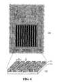
- FIG. 6illustrates an ICP layout showing one-dimensional (1D) metal pattern, integrated using metal-1 layer material, with period a and hole size d according to an embodiment of the present invention.
- FIG. 7shows another ICP layout with two-dimensional (2D) metal pattern having period ax, ay and hole size dx, dy, according to an embodiment of the present invention.
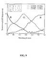
- FIG. 8shows measured ICP responsivities normalized with respect to peak photodiode response, wherein the ICP having a 2D metal pattern integrated using metal 1 layer material in accordance with an aspect of the present invention.
- FIG. 9shows transformed and normalized ICP responsivities of FIG. 8.
- FIG. 10shows measured ICP transmittances, wherein the ICP having a 1D metal pattern integrated using metal 1 layer material in accordance with an aspect of the present invention.
- the present inventionprovides a method to control pixel wavelength responsivity during the standard integrated circuit (IC) design and manufacturing process. Rather than utilizing a separate color filter (dye-based, diffraction-based, thin film-based, etc.) the wavelength responsivity is controlled using materials that are integrated into the sensor design itself. That is, the inventive method solely utilizes the semiconductor process for making an ICP image sensor.
- An ICP of the present inventionis thus distinguished from the aforementioned conventional color pixels that are constructed in at least two stages, combining a basic monochrome image sensor with a color filter array or other optical material.
- a typical image sensor pixelcomprises a light sensitive element (photodetector) that converts photons to electrons and internal circuitry that provides the pixel with desired functionality such as read-out, signal conditioning, and so forth.
- photodetectora light sensitive element
- internal circuitrythat provides the pixel with desired functionality such as read-out, signal conditioning, and so forth.
- the electrical connections between pixel componentsare routed through a series of metal layers that are between the imaging element of the system (lens) and the photodetector.
- image sensor designersintuitively attempt to keep the opening, i.e., the light receiving area of the photodetector, between the photodetector and the lens, free of metal interconnects.
- the ICP image sensor designersspecify spatial arrangements of metal wires and/or layers, i.e., metal structures, in the light path from the lens to the photodetector so that the ICP itself controls the wavelength transmission to its photodetector.
- the present inventionsimplifies the process of implementing a wavelength selective (color) pixel.
- overlaying a CFA on the image sensor pixelstakes place subsequent to the semiconductor manufacturing process and thus requires a different set of tools, materials and processing steps.
- the present inventionmakes use of the tools, materials and processing steps already available and necessary to implement “monochrome” image sensor pixels and applies them to create an ICP.
- the ability to control wavelength responsivity in this waydepends crucially on the ability to specify the width and position of the metal lines in the technology process.
- Filters made from metal lines, wire-mesh or metallic gridshave been used extensively for filtering light in the far infrared (IR) spectrum, e.g. 10 to about 800 ⁇ m wavelengths. These filters comprise thin metallic wires (much thinner than the wavelengths to be transmitted) deposited on an optically clear support for selecting wavelength and polarization direction.
- IRfar infrared
- Exemplary teachings on polarizing properties of wire gratingscan be found in “Highly conducting wire gratings in the resonance region” by Lochbihler et al., “Surface polaritons on gold-wire gratings” by Lochbihler, and “Polarimetry of transmission gratings” by Lochbihler et al., which are hereby incorporated herein by reference.
- the filtersare characterized by a wavelength transmittance having a peak at approximately 1.2 times the periodicity of the mesh. These filters would only be useful for visible imaging if this peak could be made in the visible range.
- the metal lines within the pixelare comparable or smaller than the wavelength of visible light (400 to 700 nm). At these scales, the metal layers are not as opaque to visible light as bulk metal, and variations in the pattern control the probability that incident light at a particular wavelength will influence the photodetector.
- the likelihood of the incident light influencing the photodetectoris governed by the optical properties of the metal wires and/or layers and the geometry of the patterns implemented.
- one potential explanation of the physical mechanism for the wavelength selectivityis that providing the right pattern enables an incident wave front to stimulate a collective oscillation of the electrons on the front metal surface. These oscillations are commonly referred to as surface plasmons. Excitation of plasmons occurs because of momentum transfer from the light to the plasmon. The front surface plasmon can subsequently strongly couple with the back surface plasmon through the patterned apertures in the metal layers. At the back surface, a reverse momentum transfer process results in the emission of photons that are absorbed by the photodetector.
- This surface-plasmon induced resonance phenomenonyields a peak transmittance, which occurs for a given wavelength depending on the type of metal, the dielectric surrounding and pattern geometry. Hence, the chance that a photon of a particular wavelength will influence the photodetector depends on the spatial pattern of on the metal layer and the wavelength of the photon.
- Exemplary teachings on surface-plasmon induced resonance phenomenoncan be found in the following publications, which are hereby incorporated herein by reference and collectively referred to as Ebbesen hereinafter:
- EbbesenBased on the principle of surface-plasmon induced resonance phenomenon disclosed by Ebbesen, it is possible to create thin films that control the wavelength transmittance along the light path, serving as a color filter.
- Ebbesenspecially designed metal films are used. These metal films differ greatly from the metal layers available in CCD and CMOS technologies based color image sensors. What is more, integrating metal films into individual monochrome pixels is counter-intuitive to sensor design rules. This is because by standard design rules the light receiving area of the photodetector are not to be covered by any optically thick layers including metal layers.
- the optical path itselfshould be free of any intrusion. That is, unlike the inventive ICP, a conventional sensor pixel does not allow metal layers intruding into the optical path of the photodetector.
- the metal layers and interconnect above and below the light modulating layercan intrude into the photodiode region, to the extent that the light modulating layer covers the predetermined light receiving area.
- Bawolek et al.particularly note that it is important that the other metal layers do not intrude into the non-covered optical path (the modulation window or opening) through which the light enters the photodiode.
- each ICP of the present inventionhas its own wavelength responsivity and/or wavelength transmittance and the image sensor can serve as part of a color imaging system.
- the intrinsic properties of the integrated circuitare used instead of thin film technology. Note that the use of a metal layer to control the wavelength transmittance and/or wavelength responsivity does not preclude that metal layer for use as an interconnect.
- an ICPis implemented using a standard 0.18 ⁇ m technology CMOS process.
- design rulesbegin to enable sub-visible wavelength features on metal layers. For example, metal wire width and spacing finer than 270 nm are now possible.
- the spatial scale of the metal lineshas reached the level necessary to control wavelength transmittance in the visible range (400 to 700 nm).
- Feature sizes allowed by the 0.18 ⁇ m CMOS process design rules for the metal layersenable reduction to practice of controllable wavelength-responsivity in the visible spectrum.
- CMOS image sensors utilizing the inventive ICPrequire feature sizes only possible in 0.18 ⁇ m or more advanced CMOS technology.
- the present inventionis not limited to CMOS image sensors but can also be applied to other image sensors including CCD based image sensors. It will also be understood to those of ordinary skill in the art that the principles of the present invention can be utilized to control transmission of longer wavelength signals, e.g., infrared (IR), using technologies such as 0.35 ⁇ m and 0.5 ⁇ M, providing, for example, an integrated IR image sensor.
- IRinfrared
- FIG. 4( b )An ICP circuit schematic according to an embodiment of the present invention is shown in FIG. 4( b ).
- a standard Active Pixel Sensor (APS) circuitis used.
- the output of the ICPis directly connected to a chip output via a follower amplifier.
- 3.3V thick oxide transistorsare used to reduce transistor gate leakage and to increase voltage swing.
- the circuit operation of the ICPis otherwise standard and will not be further described herein.
- FIG. 5( a )shows a design flow in which an ICP image sensor is developed and constructed.
- ICPs of the present inventiondo not need a separate color filter process such as a thin film process.
- FIG. 5( b )shows a standard pixel design process during which the individual ICPs are implemented.
- a light sensitive substrateis provided in step 510 .
- steps 520 , 530 , 540 , 550 , and 560layers poly, vias, metal-1, metal-2, and metal-3 are sequentially overlaid on top of each other.
- Layout of pixel 600is presented in FIG. 6. Standard integrated circuit design and fabrication process is well known in the art and thus is not further described here.
- FIG. 6illustrates an ICP layout 600 having a light sensitive area 610 .
- a photodetector 612is overlaid with metal structures 611 .
- the metal structures 611positioned directly above and in the optical path of the photodetector 612 , manifests an one-dimensional (1D) metal pattern with period a and hole size d.
- the metal structures 611thus operate as a patterned metal filter.
- This patterned metal filter 611controls the wavelength responsivity of the ICP 600 and is integrated into the ICP 600 itself during standard semiconductor manufacturing process using existing metal materials thereof, e.g., metal-1 layer.
- the patterned metal filter 611is not limited to using metal-1 layer material and may comprise a plurality of metal layers.
- FIG. 7shows another ICP layout 700 having a light sensitive area 710 . Similar to the ICP layout 600 , in the light sensitive area 710 a photodetector 712 is overlaid with metal structures 711 . As shown in FIG. 7, the metal structures 711 , i.e., the patterned metal filter 711 , are positioned on top and in the optical path of the photodetector 712 . The patterned metal filter 711 manifests a two-dimensional (2D) metal pattern having period ax, ay and hole size dx, dy. This patterned metal filter 711 controls the wavelength responsivity of the ICP 700 and is also integrated into the ICP 700 during standard integrated circuit process.
- 2Dtwo-dimensional
- FIG. 8shows measured ICP wavelength responsivities normalized with respect to peak photodiode response, wherein the ICP having a 2D metal pattern integrated using metal-1 layer material in accordance with an aspect of the present invention. Note that the measured responsivities of 0.05, 0.15, and 0.25 are les than 50% lower than the respective fractions of uncovered photodiode areas even though hole sizes are smaller or equal to the wavelength.
- FIG. 9shows the ICP responsivities of FIG. 8 after applying a linear transformation using an appropriate 3 ⁇ 3 matrix.
- Such linear transformationis well known in the art and thus is not further described herein.
- the transformed responsivitiesclearly demonstrate that the 2D metal-1 patterned ICPs exhibit RGB color pixel behavior peaking at 450 nm, 575 nm and 750 nm.
- FIG. 10shows measured ICP transmittances, wherein the ICP having a 1D metal pattern integrated using metal-1 layer material in accordance with an aspect of the present invention. Note that the transmittances in the visible wavelength range are around 0.50, which is slightly higher than the 0.47 fraction of uncovered photodiode area, i.e., hole area. It is observed that high transmittance 1D metal-1 patterns exhibit significant wavelength selectivity in the near-infrared wavelength range as well.
- the inventive ICPmay have patterns other than what have been shown and described in the present invention.
- 1D metal-1 patternsmay have high transmittance but little or no selectivity in the visible wavelength range, while 2D metal-1 patterns may have high selectivity but low transmittance. This design tradeoff is observed between the 1D metal-1 pattern of FIG. 6 and the 2D metal-1 pattern of FIG. 7.
- 1D patterns, 2D patterns, or a combination thereofmay be utilized by the inventive ICP's integrated metal filter (metal structures constructed over the photodetector using a single or multiple metal layer materials) to control wavelength responsivity and/or wavelength transmittance of the ICP.
- inventive ICP's integrated metal filtermetal structures constructed over the photodetector using a single or multiple metal layer materials
- patterned metal filtersallowing both high wavelength transmittance and visible wavelength responsivity will become possible, making the inventive ICP approach a potentially attractive and viable lower cost alternative to conventional color pixels constructed with a two-stage manufacturing process, i.e., a combination of image sensor process and color filter process.
- ICPs of the present inventionmay eventually be implemented in virtually all apparatuses and systems where color pixels are utilized, including a color image sensor of a digital camera, a diagnostic camera, a scanner, or a communication device.
- the integration of pixel design and color filteryields a novel integrated color pixel (ICP).
- ICPintegrated color pixel
- the metal layer(s)may comprise different 1D and 2D patterns.
- multiple patterned metal layersmay be used in sequence.
- the gratingmay be non-square and multiple gratings may be combined together, i.e., superposition of different k-vectors.
- the ICPmay be implemented with metal coating placed on micro lenses, diffraction gratings or other curved surfaces.
- the ICPsmay be combined with color filter arrays for other desired color effects.
Landscapes
- Solid State Image Pick-Up Elements (AREA)
Abstract
Description
- 1. Field of the Invention[0001]
- The present invention relates generally to a color image sensor and, more particularly, to an integrated color pixel (ICP) and a method of integrating control of wavelength responsivity into the ICP itself during a standard integrated circuit (IC) design and fabrication process.[0002]
- 2. Description of the Related Art[0003]
- A basic image sensor captures an image in gray scale. That is, the image sensor, with its monochrome pixels, generally records the image in a series of tones ranging from pure white to pure black. A color image sensor captures the image in colors with monochrome pixels and color filters. The color filters are utilized for controlling the wavelength responsivity of the individual monochrome pixels. The wavelength transmittance of the color filters, along with the other optical elements, determine the wavelength responsivity of the color channels of the color image sensor.[0004]
- A conventional way to integrate the color filters and hence the wavelength responsivity into the color image sensor is to utilize a color filter process in which a color filter array (CFA) comprising a regular array of differently colored filters is overlaid or deposited onto the monochrome pixels to separate out the colors of the light reflected from an image.[0005]
- Color filter process in general and the CFA technology in particular are well known in the art and thus are not further described herein. An exemplary teaching on color filter process for semiconductor array imaging devices can be found in U.S. Pat. No. 6,274,917, which is by Fan et al. and assigned to Semiconductor Manufacturing Company (TSMC), Hsin-Chu, Taiwan.[0006]
- The color filter pattern or patterned CFA of each color image sensor can be specifically designed to yield sharper images, truer colors, and/or any color effects desired. Most modern semiconductor image sensors, including complementary metal-oxide semiconductor (CMOS) and charge-coupled device (CCD) image sensors, utilize red, green, or blue (RGB) filters. Some image sensors in cameras use cyan, magenta, and yellow (CMYK) filters. The color patterns also vary from company to company with the most popular pattern being the Bayer mosaic pattern, taught by Bayer in U.S. Pat. No. 3,971,065 and assigned to Eastman Kodak Company, Rochester, N.Y.[0007]
- Bayer teaches a sensing array for color imaging having individual luminance- and chrominance-sensitive elements that are so intermixed that each type of element, i.e., according to sensitivity characteristics, occurs in a repeated pattern with luminance elements dominating the array. In this case, filters selectively transmissive to light in the green region of the spectrum are utilized in producing luminance-sensitive elements, and red and blue transmitting filters are used for producing a first and second chrominance-sensitive elements. In other words, in Bayer, selectively sensitized elements, i.e., individual monochrome pixels with corresponding color filters overlaid thereupon, cooperating in interlaid sampling patterns control wavelength responsivity of the color imaging array. An exemplary Bayer[0008]
mosaic pattern 100 is shown in FIG. 1(a). An exemplary application of the Bayermosaic pattern 100 utilized in a conventionalcolor pixel array 110 is shown in FIG. 1(b) wheremonochrome pixels 30 are overlaid with a CFA34. As shown in FIG. 1(b), the CFA34 is sandwiched betweenlayers Layers Layer 32 may comprise a variety of layers including additional metal layers for a variety of application-specific purposes. - As is well known in the art, one common problem associated with the use of CFA is that pixel and therefore the sensor sensitivity varies with the specific type of color. Several implementations have been proposed to enhance the pixel sensitivity. One such example can be found in U.S. Pat. No. 6,057,586, titled “Method and apparatus for employing a light shield to modulate pixel color responsivity” by Bawolek et al. and assigned to Intel Corporation of Santa Clara, Calif.[0009]
- In Bawolek et al., a light shield is utilized to modulate/modify pixel sensitivity. According Bawolet et al., a pixel cell refers to a light sensing circuit and a CFA overlaid on top of a light sensor. The light sensor, as commonly understood, can be any means that receives and converts incident light into an electrical signal representative of that light. The pixel cell having a color filter array material of a first color disposed above the light sensor has a first relative sensitivity. A modulating light shield is disposed above the light sensor to modulate the pixel sensitivity. The light shield forms an aperture whose area is substantially equal to a light receiving area of the light sensor adjusted by a reduction factor. The reduction factor is the result of an arithmetic operation between the first relative sensitivity and a second relative sensitivity, associated with a second pixel of a second color. In Bawolet et al., the light shield, constructed using one of the pixel metal layers, and the CFA overlaid thereupon control sensitivity and wavelength responsivity of the pixel, respectively. Bawolet et al. particularly note that it is important that the other metal layers do not intrude into the non-covered optical path specified by the light shield layer. FIG. 2([0010]a) shows a conventional
color pixel array 200 havingmonochrome pixels 201 overlaid with a CFA210 having a typical Bayer RGB pattern. FIG. 2(b) shows a modifiedcolor pixel array 220 comprising themonochrome pixels 201 overlaid with a lightshield metal layer 202 and the CFA210. The lightshield metal layer 202 has a plurality ofopenings 203 where the area of the openings is specifically configured based on the color responsivity, i.e., red, green, or blue, of the pixel cell. The openings employed for controlling the pixel sensitivity can range from approximately one micron by one micron to 5 microns by 5 microns. - The various pixel implementations including the aforementioned pixel sensitivity modulation layer are to improve mostly CCD technology-based or CMOS technology-based image sensors. CCD image sensors have drawbacks well known in the art including limited on-chip signal processing capability and high power consumption. CMOS image sensors have been developed to overcome these drawbacks. The advantages of CMOS image sensors over CCD image sensors are well known in the art and thus are not described herein. CMOS image sensors utilizing CFAs, however, still have the following weaknesses.[0011]
- A typical CFA may include multiple layers of superimposed color filters, which often cause a color “cross-talk” problem. Also, because the height of a pixel inversely affects the pixel's efficiency, the added height of these layers may cause a decrease in pixel efficiency.[0012]
- What is more, as discussed heretofore, a typical CMOS color image sensor generally comprises a basic “monochrome” image sensor with color filters overlaid thereupon. The hybrid nature of CMOS image sensors and the color filter process lead to high fabrication costs and inflexibility in color image sensor design flow. Utilizing thin film technology, Böhm et al. proposed in “High Dynamic Range Image Sensors in Thin Film on ASIC Technology for Automotive Applications” Thin-Film-on-ASIC (TFA) image sensors to overcome the weaknesses of conventional CMOS color image sensors and to further reduce color image sensor manufacturing costs.[0013]
- According to Böhm et al., a TFA image sensor is a vertically integrated image sensor where the optical detector of the sensor is deposited onto an ASIC wafer by a plasma enhanced chemical vapor deposition (PECVD) process in a cluster deposition system. ASIC wafer itself is fabricated using a standard 0.7 μm CMOS process.[0014]
- Thin film technology provides a possibility of retaining the entire usual design flow and fabrication steps as employed for ASICs. As shown in FIG. 3([0015]a), a typical
TFA image sensor 300 consists of an amorphous silicon (a-Si:H) basedoptical detector 310 being deposited on top of a crystalline silicon (x-Si)ASIC 301 in a low temperature PECVD process. a-Si:H is an excellent material for optical detectors but not for electronic circuits. On the other hand, x-Si has poor photoelectric properties but a wide range of highly developed and abundantly available technologies for fabricating powerful integrated circuits. - FIG. 3([0016]a) also shows the layer sequence of the typical
TFA image sensor 300 where aninsulation layer 320 separates theoptical detector 310 from theASIC 301. Theinsulation layer 320 is patterned in order to provide contact holes between theoptical detector 310 and the circuitry ofASIC 301. Generally, there is one hole per pixel. The ASIC301 typically includes identical pixel circuitry underneath each detector and peripheral circuitry outside the light sensitive area. Thethin film system 340 is sandwiched between a metalrear electrode 330, which is usually the third metal layer of theASIC 301, and a transparentfront electrode 350. Due to its higher absorption coefficient and its maximum spectral response for green light, an amorphous silicon detector is better qualified for an image sensor than a crystalline silicon detector. This thin film deposition sequence is adaptable to the specific requirement of an application. For example, the a-Si:Hthin film system 340 may comprise multiple layers. According to Böhm et al., at a thickness of less than 1 μm, the thin film system consists of four to seven successively deposited layers. - FIG. 3([0017]b) illustrates how the
TFA image sensor 300 is developed and fabricated. As shown in FIG. 3(b), theASIC 301 and theoptical detector 310 are separately developed in TFA image sensor design andfabrication process 311 so that the photoelectric properties of the detector can be optimized independent of the ASIC process. TheASIC 301 wafer is manufactured and theoptical detector 310 including the a-Si:Hthin film system 340 is subsequently deposited upon theASIC 301. TFA image sensors are suited for automotive vision systems and are in development by Silicon Vision in cooperation with the Institute for Semiconductor Electronics (IHE) at the University of Siegen, both of Germany. - According to Böhm et al., one of the major benefits of the TFA technology is the possibility to deposit thin film detectors with adjustable spectral sensitivity on top of the ASIC. For a color sensor array, this leads to a 3-colors-in-one-pixel sensor design. The spectral response can be shifted varying the voltage applied to the pixel. FIG. 4([0018]a) shows a pixel block diagram of the TFA
color sensor array 400. Thedetector circuit 410 keeps the rear electrode at constant potential in order to suppress lateral balance currents. The photocurrent is fed into one of thecolor circuits color sensor array 400 generates and stores the complete RGB information inside each pixel without intermediate readout operation. For readout, the integrated color voltages are sequentially applied to thecolumn output line 450. - Wavelength responsivity of a TFA color pixel is controlled by the thin film being deposited thereupon a standard ASIC wafer. That is, the essential ability of controlling wavelength responsivity of a color image sensor is still dependent upon a separate and independent thin film process applied subsequent to standard semiconductor processing steps. What is more, pixels in the vertically integrated TFA image sensor having multiple layers deposited thereon may suffer from reduced pixel efficiency because of the increased overall height of the pixels.[0019]
- What is needed, is a method of integrating control of wavelength responsivity into the pixel itself, generating a complete and highly integrated color pixel for quality color imaging using entirely standard semiconductor IC design and fabrication process, thereby solving a problem of color cross-talk in image sensors utilizing superimposed color filters and eliminating a need to subsequently applying a separate color filter process such as the thin film process, hence simplifying color image sensor design flow, further reducing color image sensor manufacturing cost, and potentially increasing pixel efficiency.[0020]
- Accordingly, it is a primary object of the present invention to integrate design of pixel and color filter yielding a novel integrated color pixel (ICP).[0021]
- It is also an object of the present invention to utilize patterned metal layers and/or wires as wavelength selective (color) filter inside the pixel, thereby eliminating a need for additional color filter processing steps or thin films and hence reducing the overall height of the pixel.[0022]
- It is yet another object of the present invention to provide an integrated color pixel that provides wavelength selection of light without color cross-talk.[0023]
- It is a further object of the present invention to provide an integrated color pixel, comprising a pixel having a light sensitive element and at least one integrated metal filter, wherein the metal filter having an array of holes for selectively controlling light received by the light sensitive element of the pixel and wherein the metal filter being integrated into the pixel itself during a standard integrated circuit process.[0024]
- Still another object of the present invention is to provide a method for integrating control of wavelength responsivity into a pixel itself, comprising the acts of specifying metal structures in at least one metal layer of the pixel during mask making stage of a standard semiconductor process, wherein the metal structures comprising metal materials readily available in and commonly used by the process and wherein the specifying act including spatially arranging the metal structures so as to form an array of holes manifesting a one- or two-dimensional pattern for controlling wavelength responsivity of the pixel.[0025]
- Still further objects and advantages of the present invention will become apparent to one of ordinary skill in the art upon reading and understanding the following drawings and detailed description of the preferred embodiments. As it will be appreciated by one of ordinary skill in the art, the present invention may take various forms and may comprise various components and steps and arrangements thereof. Accordingly, the drawings are for purposes of illustrating a preferred embodiment(s) of the present invention and are not to be construed as limiting the present invention.[0026]
- FIG. 1([0027]a) shows a conventional CFA with Bayer mosaic pattern.
- FIG. 1([0028]b) is a three-dimensional view of a conventional color pixel model having a CFA overlaid on top of an array of monochrome pixels.
- FIG. 2([0029]a) shows a conventional color pixel array.
- FIG. 2([0030]b) shows a prior art implementation of a color pixel array with a light shield for modulating pixel sensitivity.
- FIG. 3([0031]a) illustrates the layer sequence of a TFA image sensor.
- FIG. 3([0032]b) is a block diagram showing a typical TFA image sensor design and fabrication process.
- FIG. 4([0033]a) illustrates a TFA color pixel circuit.
- FIG. 4([0034]b) illustrates an ICP circuit comprising an APS pixel and a 2-stage follower amplifier according to an embodiment of the present invention.
- FIG. 5([0035]a) is a block diagram showing an ICP image sensor design and fabrication process according to an aspect of the present invention.
- FIG. 5([0036]b) illustrates standard semiconductor processing steps during which the inventive ICP is implemented according to an embodiment of the present invention.
- FIG. 6 illustrates an ICP layout showing one-dimensional (1D) metal pattern, integrated using metal-1 layer material, with period a and hole size d according to an embodiment of the present invention.[0037]
- FIG. 7 shows another ICP layout with two-dimensional (2D) metal pattern having period ax, ay and hole size dx, dy, according to an embodiment of the present invention.[0038]
- FIG. 8 shows measured ICP responsivities normalized with respect to peak photodiode response, wherein the ICP having a 2D metal pattern integrated using[0039]
metal 1 layer material in accordance with an aspect of the present invention. - FIG. 9 shows transformed and normalized ICP responsivities of FIG. 8.[0040]
- FIG. 10 shows measured ICP transmittances, wherein the ICP having a 1D metal pattern integrated using[0041]
metal 1 layer material in accordance with an aspect of the present invention. - The present invention provides a method to control pixel wavelength responsivity during the standard integrated circuit (IC) design and manufacturing process. Rather than utilizing a separate color filter (dye-based, diffraction-based, thin film-based, etc.) the wavelength responsivity is controlled using materials that are integrated into the sensor design itself. That is, the inventive method solely utilizes the semiconductor process for making an ICP image sensor. An ICP of the present invention is thus distinguished from the aforementioned conventional color pixels that are constructed in at least two stages, combining a basic monochrome image sensor with a color filter array or other optical material.[0042]
- As is well known in the art, a typical image sensor pixel comprises a light sensitive element (photodetector) that converts photons to electrons and internal circuitry that provides the pixel with desired functionality such as read-out, signal conditioning, and so forth. In most manufacturing processes, the electrical connections between pixel components are routed through a series of metal layers that are between the imaging element of the system (lens) and the photodetector. Ordinarily, image sensor designers intuitively attempt to keep the opening, i.e., the light receiving area of the photodetector, between the photodetector and the lens, free of metal interconnects. Counter-intuitively, the ICP image sensor designers specify spatial arrangements of metal wires and/or layers, i.e., metal structures, in the light path from the lens to the photodetector so that the ICP itself controls the wavelength transmission to its photodetector.[0043]
- By integrating control of wavelength responsivity into the pixel itself, the present invention simplifies the process of implementing a wavelength selective (color) pixel. As discussed heretofore, in conventional processing, overlaying a CFA on the image sensor pixels takes place subsequent to the semiconductor manufacturing process and thus requires a different set of tools, materials and processing steps. The present invention makes use of the tools, materials and processing steps already available and necessary to implement “monochrome” image sensor pixels and applies them to create an ICP. The ability to control wavelength responsivity in this way depends crucially on the ability to specify the width and position of the metal lines in the technology process.[0044]
- Filters made from metal lines, wire-mesh or metallic grids, have been used extensively for filtering light in the far infrared (IR) spectrum, e.g. 10 to about 800 μm wavelengths. These filters comprise thin metallic wires (much thinner than the wavelengths to be transmitted) deposited on an optically clear support for selecting wavelength and polarization direction. Exemplary teachings on polarizing properties of wire gratings can be found in “Highly conducting wire gratings in the resonance region” by Lochbihler et al., “Surface polaritons on gold-wire gratings” by Lochbihler, and “Polarimetry of transmission gratings” by Lochbihler et al., which are hereby incorporated herein by reference. The filters are characterized by a wavelength transmittance having a peak at approximately 1.2 times the periodicity of the mesh. These filters would only be useful for visible imaging if this peak could be made in the visible range.[0045]
- In modern manufacturing processes, the metal lines within the pixel are comparable or smaller than the wavelength of visible light (400 to 700 nm). At these scales, the metal layers are not as opaque to visible light as bulk metal, and variations in the pattern control the probability that incident light at a particular wavelength will influence the photodetector.[0046]
- The likelihood of the incident light influencing the photodetector is governed by the optical properties of the metal wires and/or layers and the geometry of the patterns implemented. As such, one potential explanation of the physical mechanism for the wavelength selectivity is that providing the right pattern enables an incident wave front to stimulate a collective oscillation of the electrons on the front metal surface. These oscillations are commonly referred to as surface plasmons. Excitation of plasmons occurs because of momentum transfer from the light to the plasmon. The front surface plasmon can subsequently strongly couple with the back surface plasmon through the patterned apertures in the metal layers. At the back surface, a reverse momentum transfer process results in the emission of photons that are absorbed by the photodetector.[0047]
- This surface-plasmon induced resonance phenomenon yields a peak transmittance, which occurs for a given wavelength depending on the type of metal, the dielectric surrounding and pattern geometry. Hence, the chance that a photon of a particular wavelength will influence the photodetector depends on the spatial pattern of on the metal layer and the wavelength of the photon. Exemplary teachings on surface-plasmon induced resonance phenomenon can be found in the following publications, which are hereby incorporated herein by reference and collectively referred to as Ebbesen hereinafter:[0048]
- 1. Ebbesen et al. “Extraordinary optical transmission through sub-wavelength hole arrays,” Nature (London), February 1998, Vol. 391, pp. 667-669.[0049]
- 2. Ghaemi et al. “Surface plasmons enhance optical transmission through subwavelength holes”, Physical Review B, The American Physical Society, September 1998, Vol. 58, No. 11, pp. 6779-6782.[0050]
- 3. Kim et al. “Control of optical transmission through metals perforated with subwavelength hole arrays”, Optics Letters, Optical Society of America, February 1999, Vol. 24, No. 4, pp. 256-258.[0051]
- 4. U.S. Pat. No. 5,973,316, titled “Sub-wavelength aperture arrays with enhanced light transmission” by Ebbesen et al. and assigned to NEC Research Institute, Inc. of Princeton, N.J.[0052]
- 5. U.S. Pat. No. 6,040,936, titled “Optical transmission control apparatus utilizing metal films perforated with subwavelength-diameter holes” by Kim et al. and assigned to NEC Research Institute, Inc. of Princeton, N.J.[0053]
- 6. U.S. Pat. No. 6,236,033 B1, titled “Enhanced optical transmission apparatus utilizing metal films having apertures and periodic surface topography” by Ebbesen et al. and assigned to NEC Research Institute, Inc. of Princeton, N.J.[0054]
- For decades, it has been thought that sub-wavelength apertures have very low light transmittance due to diffraction. Ebbesen's reports showed that a periodic array of holes in an optically thick metallic film exhibits extraordinary optical transmittance up to several orders of magnitude higher than small-hole diffraction theory predicts. As discussed before, such wavelength transmittance depends on the spatial arrangement, i.e., pattern, of the holes in the metal and the peak transmittance occurs at a given wavelength depending on the type of metal, the surrounding dielectric, and the geometry of the pattern.[0055]
- An important application that motivated the present invention is the design of color filters for displays. Based on the principle of surface-plasmon induced resonance phenomenon disclosed by Ebbesen, it is possible to create thin films that control the wavelength transmittance along the light path, serving as a color filter. However, in Ebbesen, specially designed metal films are used. These metal films differ greatly from the metal layers available in CCD and CMOS technologies based color image sensors. What is more, integrating metal films into individual monochrome pixels is counter-intuitive to sensor design rules. This is because by standard design rules the light receiving area of the photodetector are not to be covered by any optically thick layers including metal layers.[0056]
- Even if part of the light receiving area that is not in the optical path may be covered, the optical path itself, by standard design rules, should be free of any intrusion. That is, unlike the inventive ICP, a conventional sensor pixel does not allow metal layers intruding into the optical path of the photodetector. For example, in Bawolek et al., the metal layers and interconnect above and below the light modulating layer can intrude into the photodiode region, to the extent that the light modulating layer covers the predetermined light receiving area. As discussed herein, Bawolek et al. particularly note that it is important that the other metal layers do not intrude into the non-covered optical path (the modulation window or opening) through which the light enters the photodiode.[0057]
- We have discovered that, notwithstanding standard sensor pixel design rules, it is possible to integrate control of the wavelength responsivity into the pixel design, taking advantage of the multiple metal layers present in a standard integrated circuit such as a CMOS image sensor. The present invention thus significantly extends the application of the surface-plasmon induced resonance phenomenon from thin films to the design of a complete integrated optical detector circuit.[0058]
- Specifically, during the design process, e.g., during standard mask preparation, one can use the ability to specify metal structures in the layers above the photodetector, for example, a photodiode, to control the relative wavelength responsivity. By appropriately choosing/designing the metal structures, each ICP of the present invention has its own wavelength responsivity and/or wavelength transmittance and the image sensor can serve as part of a color imaging system. In this novel application, the intrinsic properties of the integrated circuit are used instead of thin film technology. Note that the use of a metal layer to control the wavelength transmittance and/or wavelength responsivity does not preclude that metal layer for use as an interconnect.[0059]
- In an exemplary embodiment of the present invention, an ICP is implemented using a standard 0.18 μm technology CMOS process. At 0.18 μm, design rules begin to enable sub-visible wavelength features on metal layers. For example, metal wire width and spacing finer than 270 nm are now possible. Additionally, using the 0.18 μm CMOS technology, the spatial scale of the metal lines has reached the level necessary to control wavelength transmittance in the visible range (400 to 700 nm). Feature sizes allowed by the 0.18 μm CMOS process design rules for the metal layers enable reduction to practice of controllable wavelength-responsivity in the visible spectrum. Accordingly, implementations of CMOS image sensors utilizing the inventive ICP require feature sizes only possible in 0.18 μm or more advanced CMOS technology. On the other hand, it will be understood to those of ordinary skill in the art that the present invention is not limited to CMOS image sensors but can also be applied to other image sensors including CCD based image sensors. It will also be understood to those of ordinary skill in the art that the principles of the present invention can be utilized to control transmission of longer wavelength signals, e.g., infrared (IR), using technologies such as 0.35 μm and 0.5 μM, providing, for example, an integrated IR image sensor.[0060]
- An ICP circuit schematic according to an embodiment of the present invention is shown in FIG. 4([0061]b). In FIG. 4(b), a standard Active Pixel Sensor (APS) circuit is used. The output of the ICP is directly connected to a chip output via a follower amplifier. 3.3V thick oxide transistors are used to reduce transistor gate leakage and to increase voltage swing. The circuit operation of the ICP is otherwise standard and will not be further described herein.
- FIG. 5([0062]a) shows a design flow in which an ICP image sensor is developed and constructed. As illustrated in FIG. 5(a), by controlling wavelength responsivity in the pixel design process, ICPs of the present invention do not need a separate color filter process such as a thin film process. FIG. 5(b) shows a standard pixel design process during which the individual ICPs are implemented. As illustrated in FIG. 5(b), a light sensitive substrate is provided in
step 510. Subsequently, insteps pixel 600 is presented in FIG. 6. Standard integrated circuit design and fabrication process is well known in the art and thus is not further described here. - FIG. 6 illustrates an[0063]
ICP layout 600 having a lightsensitive area 610. According to an embodiment of the present invention, in the light sensitive area610 aphotodetector 612 is overlaid withmetal structures 611. As shown in FIG. 6, themetal structures 611, positioned directly above and in the optical path of thephotodetector 612, manifests an one-dimensional (1D) metal pattern with period a and hole size d. Themetal structures 611 thus operate as a patterned metal filter. Thispatterned metal filter 611 controls the wavelength responsivity of theICP 600 and is integrated into theICP 600 itself during standard semiconductor manufacturing process using existing metal materials thereof, e.g., metal-1 layer. As it will be understood by one of ordinary skill in the art, the patternedmetal filter 611 is not limited to using metal-1 layer material and may comprise a plurality of metal layers. - FIG. 7 shows another[0064]
ICP layout 700 having a lightsensitive area 710. Similar to theICP layout 600, in the light sensitive area710 aphotodetector 712 is overlaid withmetal structures 711. As shown in FIG. 7, themetal structures 711, i.e., the patternedmetal filter 711, are positioned on top and in the optical path of thephotodetector 712. The patternedmetal filter 711 manifests a two-dimensional (2D) metal pattern having period ax, ay and hole size dx, dy. Thispatterned metal filter 711 controls the wavelength responsivity of theICP 700 and is also integrated into theICP 700 during standard integrated circuit process. - In another embodiment of the present invention, several 1D and 2D metal patterns with periodicity ranging from a=540 nm to 810 nm and spacing from d=270 nm to 540 nm and using different metal layers were deposited on top of APS photodetectors of 6 and 12 μm ICPs with n+/pwell photodiodes, respectively. FIG. 8 shows measured ICP wavelength responsivities normalized with respect to peak photodiode response, wherein the ICP having a 2D metal pattern integrated using metal-1 layer material in accordance with an aspect of the present invention. Note that the measured responsivities of 0.05, 0.15, and 0.25 are les than 50% lower than the respective fractions of uncovered photodiode areas even though hole sizes are smaller or equal to the wavelength.[0065]
- FIG. 9 shows the ICP responsivities of FIG. 8 after applying a linear transformation using an appropriate 3×3 matrix. Such linear transformation is well known in the art and thus is not further described herein. The transformed responsivities clearly demonstrate that the 2D metal-1 patterned ICPs exhibit RGB color pixel behavior peaking at 450 nm, 575 nm and 750 nm.[0066]
- FIG. 10 shows measured ICP transmittances, wherein the ICP having a 1D metal pattern integrated using metal-1 layer material in accordance with an aspect of the present invention. Note that the transmittances in the visible wavelength range are around 0.50, which is slightly higher than the 0.47 fraction of uncovered photodiode area, i.e., hole area. It is observed that high transmittance 1D metal-1 patterns exhibit significant wavelength selectivity in the near-infrared wavelength range as well.[0067]
- Accordingly, it has been demonstrated that placing metal patterns on top of a photodetector can significantly influence its wavelength responsivity. Further, as evidenced by these ICP responsivity measurements, with additional signal processing one can obtain responsivities that are suitable for color imaging. As will be understood by one with ordinary skill in the art, the inventive ICP may have patterns other than what have been shown and described in the present invention. Note 1D metal-1 patterns may have high transmittance but little or no selectivity in the visible wavelength range, while 2D metal-1 patterns may have high selectivity but low transmittance. This design tradeoff is observed between the 1D metal-1 pattern of FIG. 6 and the 2D metal-1 pattern of FIG. 7. Thus, depending upon design specifications, 1D patterns, 2D patterns, or a combination thereof may be utilized by the inventive ICP's integrated metal filter (metal structures constructed over the photodetector using a single or multiple metal layer materials) to control wavelength responsivity and/or wavelength transmittance of the ICP. Furthermore, it is anticipated that, with more advanced processes providing finer metal width, spacing, and thickness, patterned metal filters allowing both high wavelength transmittance and visible wavelength responsivity will become possible, making the inventive ICP approach a potentially attractive and viable lower cost alternative to conventional color pixels constructed with a two-stage manufacturing process, i.e., a combination of image sensor process and color filter process. Accordingly, ICPs of the present invention may eventually be implemented in virtually all apparatuses and systems where color pixels are utilized, including a color image sensor of a digital camera, a diagnostic camera, a scanner, or a communication device.[0068]
- In conclusion, the integration of pixel design and color filter yields a novel integrated color pixel (ICP). Using metal materials, e.g., metal layers and/or wires, already available for standard semiconductor process to specify and fabricate an integrated wavelength selective (color) filter inside the pixel enables the elimination of additional color filter processing steps or thin films. As such, the overall height of the pixel is reduced and hence potentially increases pixel efficiency. The ICP also avoids color cross-talk since the color filter is integrated and not superimposed.[0069]
- Although the present invention and its advantages have been described in detail, it should be understood that various changes, substitutions, and alternations could be made herein without departing from the principle and the scope of the invention. For example, different available metal layers may be utilized. The metal layer(s) may comprise different 1D and 2D patterns. In addition, multiple patterned metal layers may be used in sequence. The grating may be non-square and multiple gratings may be combined together, i.e., superposition of different k-vectors. In some embodiments, the ICP may be implemented with metal coating placed on micro lenses, diffraction gratings or other curved surfaces. In other embodiments, the ICPs may be combined with color filter arrays for other desired color effects. What is more, although approximately ninety percent of the layers that can be controlled during the design stage are metal layers, there are non-metal layers that a sensor designer might be able to have some, probably more restricted, control. Therefore, it is anticipated that patterns on any of the layers, including metal and non-metal ones, used in the standard integrated circuit process may be utilized to control the pixel's wavelength transmittance and wavelength responsivity.[0070]
- Accordingly, the scope of the present invention should be determined by the following claims and their legal equivalents.[0071]
Claims (20)
1. An integrated color pixel (ICP), comprising:
a pixel having a light sensing means and at least one filter means, wherein
said filter means having an array of holes for selectively controlling wavelength transmittance and wavelength responsivity and wherein
said filter means being integrated into said pixel during an industry-standard integrated circuit (IC) process thereby eliminating a need to obtain a separate color filter means subsequent to said IC process.
2. The ICP ofclaim 1 , wherein said light sensing means comprising a photodetector with a light receiving area and wherein said filter means being positioned on top of said light receiving area.
3. The ICP ofclaim 1 , wherein said filter means being part of at least one metal layer above said light sensing means.
4. The ICP ofclaim 1 , wherein said filter means comprising materials used by said IC process and wherein said array of holes manifesting a one- or two-dimensional pattern.
5. The ICP ofclaim 4 , wherein said materials comprising metal wires spatially arranged to form said pattern on top of said light sensing means.
6. The ICP ofclaim 4 , wherein said materials comprising metal structures spatially arranged to form said pattern, said spatial arrangement being specified during industry-standard mask preparation of said IC process.
7. The ICP ofclaim 1 , wherein said array of holes manifesting a one- or two-dimensional pattern.
8. The ICP ofclaim 1 , wherein said process being a complementary metal-oxide semiconductor (CMOS) process.
9. The ICP ofclaim 1 , wherein said process being a charge-coupled device (CCD) process.
10. The ICP ofclaim 1 , wherein said ICP is implemented in a color image sensor of a color imaging device including a digital camera, a diagnostic camera, a scanner, or a image recorder.
11. A method for integrating a color filter into a pixel having at least one metal layer and a light sensing means, comprising:
specifying, during an industry-standard integrated circuit (IC) process and notwithstanding design rules of said process, a array of holes spatially arranged in said metal layer above said light sensing means for selectively controlling wavelength detected by said light sensing means; and
fabricating said metal layer and said pixel substantially simultaneously during said IC process thereby generating an integrated color pixel (ICP) without a subsequent color filter process.
12. The method ofclaim 11 , wherein said at least one metal layer comprising metal materials used by said IC process, wherein said light sensing means comprising a photodetector and wherein said array of holes manifesting a one- or two-dimensional pattern on top of said light receiving area.
13. The method ofclaim 12 , wherein said metal material comprising metal wires spatially arranged to form said pattern.
14. The method ofclaim 12 , wherein said metal material comprising metal structures spatially arranged to form said pattern, said spatial arrangement being specified using industry-standard photo-masking preparation software during said IC process.
15. The method ofclaim 11 , wherein said light sensing means comprising a photodetector with a light receiving area and wherein said metal filter means being positioned above said light receiving area.
16. The method ofclaim 11 , wherein said IC process being a complementary metal-oxide semiconductor (CMOS) process.
17. The method ofclaim 11 , wherein said IC process being a charge-coupled device (CCD) process.
18. A method for generating an integrated color image sensor, comprising:
controlling wavelength transmittance and wavelength responsivities of said integrated color image sensor by specifying metal structures of said sensor during a standardized image sensor design stage of a standardized image sensor fabrication process, wherein
said metal structures comprising metal materials used by said process and wherein
said specifying act further comprising spatially arranging said metal structures so as to form an array of holes manifesting a one- or two-dimensional pattern for enabling said controlling act.
19. The method ofclaim 18 , further comprising:
fabricating said metal structures and said integrated color image sensor substantially simultaneously during said process thereby eliminating a need to obtain a separate color filter for said sensor subsequent to said process.
20. The method ofclaim 18 , wherein said integrated color image sensor comprising a photodetector with a light receiving area and wherein said metal structures being positioned on top of said light receiving area.
Priority Applications (1)
| Application Number | Priority Date | Filing Date | Title |
|---|---|---|---|
| US09/999,592US7248297B2 (en) | 2001-11-30 | 2001-11-30 | Integrated color pixel (ICP) |
Applications Claiming Priority (1)
| Application Number | Priority Date | Filing Date | Title |
|---|---|---|---|
| US09/999,592US7248297B2 (en) | 2001-11-30 | 2001-11-30 | Integrated color pixel (ICP) |
Publications (2)
| Publication Number | Publication Date |
|---|---|
| US20030103150A1true US20030103150A1 (en) | 2003-06-05 |
| US7248297B2 US7248297B2 (en) | 2007-07-24 |
Family
ID=25546503
Family Applications (1)
| Application Number | Title | Priority Date | Filing Date |
|---|---|---|---|
| US09/999,592Expired - LifetimeUS7248297B2 (en) | 2001-11-30 | 2001-11-30 | Integrated color pixel (ICP) |
Country Status (1)
| Country | Link |
|---|---|
| US (1) | US7248297B2 (en) |
Cited By (88)
| Publication number | Priority date | Publication date | Assignee | Title |
|---|---|---|---|---|
| US20040121507A1 (en)* | 2002-12-18 | 2004-06-24 | Bude Jeffrey Devin | Semiconductor devices with reduced active region deffects and unique contacting schemes |
| US20050062863A1 (en)* | 2003-09-19 | 2005-03-24 | Fuji Photo Film Co., Ltd. | Solid state imaging device |
| WO2005029541A2 (en) | 2003-08-14 | 2005-03-31 | Microspectral Sensing, Llc | System and method for integrated sensing and control of industrial processes |
| US20050086628A1 (en)* | 2003-10-16 | 2005-04-21 | Filippi Ronald G.Jr. | Method of extracting properties of back end of line (BEOL) chip architecture |
| US20050121599A1 (en)* | 2003-12-03 | 2005-06-09 | Chandra Mouli | Metal mesh filter-comprising semiconductor image sensor |
| US20050205954A1 (en)* | 2002-12-18 | 2005-09-22 | King Clifford A | Image sensor comprising isolated germanium photodetectors integrated with a silicon substrate and silicon circuitry |
| US20060169870A1 (en)* | 2005-02-01 | 2006-08-03 | Silsby Christopher D | Image sensor with embedded optical element |
| US7110154B2 (en) | 2004-06-10 | 2006-09-19 | Clemson University | Plasmon-photon coupled optical devices |
| US20060249654A1 (en)* | 2005-05-06 | 2006-11-09 | Silsby Christopher D | Pixel with spatially varying sensor positions |
| US20070034518A1 (en)* | 2005-08-15 | 2007-02-15 | Virgin Islands Microsystems, Inc. | Method of patterning ultra-small structures |
| US20070035653A1 (en)* | 2005-08-11 | 2007-02-15 | Micron Technology, Inc. | High dynamic range imaging device using multiple pixel cells |
| EP1758372A1 (en)* | 2005-08-23 | 2007-02-28 | OmniVision Technologies, Inc. | Method and apparatus for reducing optical crosstalk in cmos image sensors |
| US20070045642A1 (en)* | 2005-08-25 | 2007-03-01 | Micron Technology, Inc. | Solid-state imager and formation method using anti-reflective film for optical crosstalk reduction |
| US20070065921A1 (en)* | 2000-09-12 | 2007-03-22 | Massachusetts Institute Of Technology | Methods and products related to producing low molecular weight heparin |
| US7214920B2 (en) | 2005-05-06 | 2007-05-08 | Micron Technology, Inc. | Pixel with spatially varying metal route positions |
| US20070152781A1 (en)* | 2006-01-05 | 2007-07-05 | Virgin Islands Microsystems, Inc. | Switching micro-resonant structures by modulating a beam of charged particles |
| US20070164377A1 (en)* | 2006-01-13 | 2007-07-19 | Gruhlke Russell W | Semiconductor sensor using surface plasmons to increase energy absorption efficiency |
| US20070200940A1 (en)* | 2006-02-28 | 2007-08-30 | Gruhlke Russell W | Vertical tri-color sensor |
| WO2007118895A1 (en)* | 2006-04-19 | 2007-10-25 | Commissariat A L'energie Atomique | Microstructured spectral filter and image sensor |
| US20070253535A1 (en)* | 2006-04-26 | 2007-11-01 | Virgin Islands Microsystems, Inc. | Source of x-rays |
| US20070258690A1 (en)* | 2006-05-05 | 2007-11-08 | Virgin Islands Microsystems, Inc. | Integration of electromagnetic detector on integrated chip |
| US20070257738A1 (en)* | 2006-05-05 | 2007-11-08 | Virgin Islands Microsystems, Inc. | Top metal layer shield for ultra-small resonant structures |
| US20070257283A1 (en)* | 2006-05-03 | 2007-11-08 | Taiwan Semiconductor Manufacturing Company, Ltd. | Color filter-embedded MSM image sensor |
| US20070258675A1 (en)* | 2006-05-05 | 2007-11-08 | Virgin Islands Microsystems, Inc. | Multiplexed optical communication between chips on a multi-chip module |
| US20080055455A1 (en)* | 2006-08-31 | 2008-03-06 | Micron Technology, Inc. | Imbalance determination and correction in image sensing |
| US20080198454A1 (en)* | 2007-02-19 | 2008-08-21 | Taiwan Semiconductor Manufacturing Company, Ltd. | Color Filter For Image Sensor |
| US20080217712A1 (en)* | 2007-03-07 | 2008-09-11 | Giuseppe Rossi | Apparatus and method for forming optical black pixels with uniformly low dark current |
| JP2008233049A (en)* | 2007-03-23 | 2008-10-02 | Canon Inc | Photodetection element, photodetection method, imaging element, and imaging method |
| US20080265146A1 (en)* | 2003-08-14 | 2008-10-30 | Microptix Technologies, Llc | Integrated sensing module for handheld spectral measurements |
| WO2009011439A1 (en)* | 2007-07-13 | 2009-01-22 | Canon Kabushiki Kaisha | Optical filter |
| WO2008114148A3 (en)* | 2007-03-22 | 2009-02-12 | Univ Pasteur | Device for sorting and concentrating electromagnetic energy and apparatus comprising at least one such device |
| US20090086064A1 (en)* | 2007-09-27 | 2009-04-02 | Micron Technology, Inc. | Dynamic adaptive color filter array |
| US20090091644A1 (en)* | 2007-10-05 | 2009-04-09 | Mackey Jeffrey L | Metallic nanostructure color filter array and method of making the same |
| US20090108203A1 (en)* | 2007-10-31 | 2009-04-30 | Gregoire Daniel J | Multiple-band detector using frequency selective slots |
| US7558490B2 (en) | 2006-04-10 | 2009-07-07 | Virgin Islands Microsystems, Inc. | Resonant detector for optical signals |
| US7557365B2 (en) | 2005-09-30 | 2009-07-07 | Virgin Islands Microsystems, Inc. | Structures and methods for coupling energy from an electromagnetic wave |
| US7557647B2 (en) | 2006-05-05 | 2009-07-07 | Virgin Islands Microsystems, Inc. | Heterodyne receiver using resonant structures |
| US7560716B2 (en) | 2006-09-22 | 2009-07-14 | Virgin Islands Microsystems, Inc. | Free electron oscillator |
| US7569836B2 (en) | 2006-05-05 | 2009-08-04 | Virgin Islands Microsystems, Inc. | Transmission of data between microchips using a particle beam |
| US7573045B2 (en) | 2006-05-15 | 2009-08-11 | Virgin Islands Microsystems, Inc. | Plasmon wave propagation devices and methods |
| US20090200585A1 (en)* | 2008-02-08 | 2009-08-13 | Omnivision Technologies, Inc. | Backside illuminated imaging sensor with backside p+ doped layer |
| US7579609B2 (en) | 2005-12-14 | 2009-08-25 | Virgin Islands Microsystems, Inc. | Coupling light of light emitting resonator to waveguide |
| US7583370B2 (en) | 2006-05-05 | 2009-09-01 | Virgin Islands Microsystems, Inc. | Resonant structures and methods for encoding signals into surface plasmons |
| US7586167B2 (en)* | 2006-05-05 | 2009-09-08 | Virgin Islands Microsystems, Inc. | Detecting plasmons using a metallurgical junction |
| US7586097B2 (en) | 2006-01-05 | 2009-09-08 | Virgin Islands Microsystems, Inc. | Switching micro-resonant structures using at least one director |
| WO2009122381A1 (en)* | 2008-04-03 | 2009-10-08 | Nxp B.V. | Spectrally-sensitive light filter arrangement and approach therefor |
| US7605835B2 (en) | 2006-02-28 | 2009-10-20 | Virgin Islands Microsystems, Inc. | Electro-photographic devices incorporating ultra-small resonant structures |
| US7616855B2 (en) | 2004-11-15 | 2009-11-10 | Avago Technologies General Ip (Singapore) Pte. Ltd. | Integrated waveguide and method for designing integrated waveguide |
| US7619373B2 (en) | 2006-01-05 | 2009-11-17 | Virgin Islands Microsystems, Inc. | Selectable frequency light emitter |
| US7626179B2 (en) | 2005-09-30 | 2009-12-01 | Virgin Island Microsystems, Inc. | Electron beam induced resonance |
| US20090323060A1 (en)* | 2006-08-02 | 2009-12-31 | Dietmar Knipp | Spectral optical sensor and method for producing an optical spectral sensor |
| US7646991B2 (en) | 2006-04-26 | 2010-01-12 | Virgin Island Microsystems, Inc. | Selectable frequency EMR emitter |
| US7655934B2 (en) | 2006-06-28 | 2010-02-02 | Virgin Island Microsystems, Inc. | Data on light bulb |
| US7656094B2 (en) | 2006-05-05 | 2010-02-02 | Virgin Islands Microsystems, Inc. | Electron accelerator for ultra-small resonant structures |
| US7659513B2 (en) | 2006-12-20 | 2010-02-09 | Virgin Islands Microsystems, Inc. | Low terahertz source and detector |
| FR2935809A1 (en)* | 2008-09-11 | 2010-03-12 | Commissariat Energie Atomique | NANOSTRUCTURE SPECTRAL FILTER AND IMAGE SENSOR |
| US7679067B2 (en) | 2006-05-26 | 2010-03-16 | Virgin Island Microsystems, Inc. | Receiver array using shared electron beam |
| US7688274B2 (en) | 2006-02-28 | 2010-03-30 | Virgin Islands Microsystems, Inc. | Integrated filter in antenna-based detector |
| US7710040B2 (en) | 2006-05-05 | 2010-05-04 | Virgin Islands Microsystems, Inc. | Single layer construction for ultra small devices |
| US7718977B2 (en) | 2006-05-05 | 2010-05-18 | Virgin Island Microsystems, Inc. | Stray charged particle removal device |
| US7728702B2 (en) | 2006-05-05 | 2010-06-01 | Virgin Islands Microsystems, Inc. | Shielding of integrated circuit package with high-permeability magnetic material |
| US7728397B2 (en) | 2006-05-05 | 2010-06-01 | Virgin Islands Microsystems, Inc. | Coupled nano-resonating energy emitting structures |
| US7732786B2 (en) | 2006-05-05 | 2010-06-08 | Virgin Islands Microsystems, Inc. | Coupling energy in a plasmon wave to an electron beam |
| US7741934B2 (en) | 2006-05-05 | 2010-06-22 | Virgin Islands Microsystems, Inc. | Coupling a signal through a window |
| US7746532B2 (en) | 2006-05-05 | 2010-06-29 | Virgin Island Microsystems, Inc. | Electro-optical switching system and method |
| US7791291B2 (en) | 2005-09-30 | 2010-09-07 | Virgin Islands Microsystems, Inc. | Diamond field emission tip and a method of formation |
| US7791053B2 (en) | 2007-10-10 | 2010-09-07 | Virgin Islands Microsystems, Inc. | Depressed anode with plasmon-enabled devices such as ultra-small resonant structures |
| US20100252514A1 (en)* | 2009-04-03 | 2010-10-07 | Min-Ju Chung | Foldable baseball equipment rack |
| US20100276598A1 (en)* | 2009-04-30 | 2010-11-04 | Raytheon Company | Nano-antenna for wideband coherent conformal ir detector arrays |
| US20100276595A1 (en)* | 2009-04-30 | 2010-11-04 | Raytheon Company | Multi-band sub-wavelength ir detector having frequency selective slots and method of making the same |
| US7876793B2 (en) | 2006-04-26 | 2011-01-25 | Virgin Islands Microsystems, Inc. | Micro free electron laser (FEL) |
| EP2293032A1 (en) | 2009-09-04 | 2011-03-09 | Radisens Diagnostic Limited | An Integrated Cytometric Sensor System and Method |
| US7986113B2 (en) | 2006-05-05 | 2011-07-26 | Virgin Islands Microsystems, Inc. | Selectable frequency light emitter |
| US7990336B2 (en) | 2007-06-19 | 2011-08-02 | Virgin Islands Microsystems, Inc. | Microwave coupled excitation of solid state resonant arrays |
| US8188431B2 (en) | 2006-05-05 | 2012-05-29 | Jonathan Gorrell | Integration of vacuum microelectronic device with integrated circuit |
| US8673217B2 (en)* | 2007-10-18 | 2014-03-18 | Hewlett-Packard Development Company, L.P. | Sensor using plasmon resonance |
| US8879152B2 (en) | 2010-07-15 | 2014-11-04 | Fraunhofer-Gesellschaft Zur Foerderung Der Angewandten Forschung E.V. | Optical bandpass filter system, in particular for multichannel spectral-selective measurements |
| EP2881990A1 (en) | 2013-12-04 | 2015-06-10 | STmicroelectronics SA | Method for producing a built-in imaging device with front illumination comprising at least one metal optical filter, and corresponding device |
| JP2015200816A (en)* | 2014-04-09 | 2015-11-12 | 凸版印刷株式会社 | Structural color filter and optical instrument using the same |
| WO2015195417A1 (en)* | 2014-06-20 | 2015-12-23 | Rambus Inc. | Systems and methods for lensed and lensless optical sensing |
| EP3024029A1 (en)* | 2014-11-19 | 2016-05-25 | ams AG | Semiconductor device comprising an aperture array and method of producing such a semiconductor device |
| US9448346B2 (en) | 2012-12-19 | 2016-09-20 | Viavi Solutions Inc. | Sensor device including one or more metal-dielectric optical filters |
| US9568362B2 (en) | 2012-12-19 | 2017-02-14 | Viavi Solutions Inc. | Spectroscopic assembly and method |
| US10197716B2 (en) | 2012-12-19 | 2019-02-05 | Viavi Solutions Inc. | Metal-dielectric optical filter, sensor device, and fabrication method |
| TWI688088B (en)* | 2019-07-24 | 2020-03-11 | 晶相光電股份有限公司 | Image sensing device and image sensing system |
| CN113450696A (en)* | 2020-05-20 | 2021-09-28 | 重庆康佳光电技术研究院有限公司 | Sub-pixel structure and display |
| DE102020118842A1 (en) | 2020-07-16 | 2022-01-20 | Fraunhofer-Gesellschaft zur Förderung der angewandten Forschung eingetragener Verein | Optical filter with nanostructured layers and spectral sensor with such layers |
| US11610534B2 (en) | 2020-05-20 | 2023-03-21 | Chongqing Konka Photoelectric Technology Research Institute Co., Ltd. | Display having sub-pixel structure with a plurality of light emitting elements |
Families Citing this family (34)
| Publication number | Priority date | Publication date | Assignee | Title |
|---|---|---|---|---|
| WO2004008540A1 (en)* | 2002-07-16 | 2004-01-22 | Stmicroelectronics Nv | Tfa image sensor with stability-optimized photodiode |
| JP4711657B2 (en)* | 2004-09-29 | 2011-06-29 | パナソニック株式会社 | Solid-state imaging device |
| US20090159799A1 (en)* | 2007-12-19 | 2009-06-25 | Spectral Instruments, Inc. | Color infrared light sensor, camera, and method for capturing images |
| US7675024B2 (en)* | 2008-04-23 | 2010-03-09 | Aptina Imaging Corporation | Method and apparatus providing color filter array with non-uniform color filter sizes |
| JP4770928B2 (en)* | 2009-01-13 | 2011-09-14 | ソニー株式会社 | Optical element and solid-state image sensor |
| TW201035528A (en)* | 2009-03-25 | 2010-10-01 | Tyntek Corp | Output ratio adjustment method of a light sensor |
| KR101338117B1 (en)* | 2009-10-29 | 2013-12-06 | 엘지디스플레이 주식회사 | Liquid crystal display device and method of fabricating the same |
| KR101649696B1 (en)* | 2009-10-29 | 2016-08-22 | 엘지디스플레이 주식회사 | Fringe field switching liquid crystal display device and method of fabricating the same |
| KR101640814B1 (en)* | 2009-10-30 | 2016-07-20 | 엘지디스플레이 주식회사 | Color filter using surface plasmon and liquid crystal display device |
| KR101658532B1 (en)* | 2009-10-30 | 2016-09-23 | 엘지디스플레이 주식회사 | Method of fabricating color filter using surface plasmon and method of fabricating liquid crystal display device |
| KR101272052B1 (en)* | 2009-12-18 | 2013-06-05 | 엘지디스플레이 주식회사 | Method of fabricating color filter using surface plasmon and method of fabricating liquid crystal display device |
| KR101274591B1 (en)* | 2009-12-18 | 2013-06-13 | 엘지디스플레이 주식회사 | Color filter using surface plasmon and liquid crystal display device, and method of fabricating the same |
| KR101313654B1 (en)* | 2009-12-18 | 2013-10-02 | 엘지디스플레이 주식회사 | Color filter using surface plasmon and liquid crystal display device, and method of fabricating the same |
| WO2011139785A2 (en)* | 2010-04-27 | 2011-11-10 | The Regents Of The University Of Michigan | Display device having plasmonic color filters and photovoltaic capabilities |
| KR20140031899A (en) | 2011-04-20 | 2014-03-13 | 더 리젠츠 오브 더 유니버시티 오브 미시건 | Spectrum filtering for visual displays and imaging having minimal angle dependence |
| JP6080343B2 (en)* | 2011-07-29 | 2017-02-15 | ソニーセミコンダクタソリューションズ株式会社 | Image sensor and manufacturing method thereof |
| EP2772939B1 (en) | 2013-03-01 | 2016-10-19 | Ams Ag | Semiconductor device for detection of radiation and method of producing a semiconductor device for detection of radiation |
| US9547107B2 (en) | 2013-03-15 | 2017-01-17 | The Regents Of The University Of Michigan | Dye and pigment-free structural colors and angle-insensitive spectrum filters |
| US10638093B2 (en) | 2013-09-26 | 2020-04-28 | Rosemount Inc. | Wireless industrial process field device with imaging |
| US10823592B2 (en) | 2013-09-26 | 2020-11-03 | Rosemount Inc. | Process device with process variable measurement using image capture device |
| US11076113B2 (en) | 2013-09-26 | 2021-07-27 | Rosemount Inc. | Industrial process diagnostics using infrared thermal sensing |
| US9857228B2 (en) | 2014-03-25 | 2018-01-02 | Rosemount Inc. | Process conduit anomaly detection using thermal imaging |
| US10914635B2 (en) | 2014-09-29 | 2021-02-09 | Rosemount Inc. | Wireless industrial process monitor |
| CN107113408B (en)* | 2015-01-13 | 2021-05-11 | 索尼公司 | Image processing device, image processing method, program and system |
| US20160255323A1 (en) | 2015-02-26 | 2016-09-01 | Dual Aperture International Co. Ltd. | Multi-Aperture Depth Map Using Blur Kernels and Down-Sampling |
| GB201611511D0 (en) | 2016-03-10 | 2016-08-17 | Gooee Ltd | Universal smart lighting gateway |
| US10321535B2 (en) | 2016-03-11 | 2019-06-11 | Gooee Limited | Devices, systems, and methods for maintaining luminaire color temperature levels in a gateway based system |
| US10021757B2 (en) | 2016-03-11 | 2018-07-10 | Gooee Limited | System and method for predicting emergency lighting fixture life expectancy |
| US10047921B2 (en) | 2016-03-11 | 2018-08-14 | Gooee Limited | System and method for performing self-test and predicting emergency lighting fixtures life expectancy |
| US10021758B2 (en) | 2016-03-11 | 2018-07-10 | Gooee Limited | Sensor board for luminaire/lighting system |
| US10159134B2 (en) | 2016-03-11 | 2018-12-18 | Gooee Limited | End of life prediction system for luminaire drivers |
| GB201611513D0 (en) | 2016-03-11 | 2016-08-17 | Gooee Ltd | Colour based half life prediction system |
| US10237939B2 (en) | 2016-03-11 | 2019-03-19 | Gooee Limited | Devices, systems, and methods for maintaining light intensity in a gateway based lighting system |
| US9992843B2 (en) | 2016-03-11 | 2018-06-05 | Gooee Limited | Location independent lighting sensor system |
Citations (21)
| Publication number | Priority date | Publication date | Assignee | Title |
|---|---|---|---|---|
| US3971065A (en)* | 1975-03-05 | 1976-07-20 | Eastman Kodak Company | Color imaging array |
| US4343890A (en)* | 1978-07-24 | 1982-08-10 | Rca Corporation | Method for making planar optical waveguide comprising thin metal oxide film incorporating a relief phase grating |
| US4772951A (en)* | 1986-03-31 | 1988-09-20 | Kabushiki Kaisha Toshiba | Solid state image sensor with cell array of amorphous semiconductor photoelectric converting elements |
| US5479524A (en)* | 1993-08-06 | 1995-12-26 | Farrell; Joyce E. | Method and apparatus for identifying the color of an image |
| US5521640A (en)* | 1994-10-31 | 1996-05-28 | At&T Global Information Solutions Company | Color image array scanner with high resolution monochrome mode |
| US5734155A (en)* | 1995-06-07 | 1998-03-31 | Lsi Logic Corporation | Photo-sensitive semiconductor integrated circuit substrate and systems containing the same |
| US5761270A (en)* | 1993-09-09 | 1998-06-02 | Unfors Instruments Ab | Method and apparatus for measuring X-ray radiation |
| US5973316A (en)* | 1997-07-08 | 1999-10-26 | Nec Research Institute, Inc. | Sub-wavelength aperture arrays with enhanced light transmission |
| US5998806A (en)* | 1996-04-09 | 1999-12-07 | Forschungszentrum Julich Gmbh | Three-color sensor with a pin or nip series of layers |
| US6040936A (en)* | 1998-10-08 | 2000-03-21 | Nec Research Institute, Inc. | Optical transmission control apparatus utilizing metal films perforated with subwavelength-diameter holes |
| US6057586A (en)* | 1997-09-26 | 2000-05-02 | Intel Corporation | Method and apparatus for employing a light shield to modulate pixel color responsivity |
| US6091093A (en)* | 1999-06-01 | 2000-07-18 | Intel Corporation | Photodiode having transparent insulating film around gate islands above p-n junction |
| US6097145A (en)* | 1998-04-27 | 2000-08-01 | Copytele, Inc. | Aerogel-based phase transition flat panel display |
| US6236033B1 (en)* | 1998-12-09 | 2001-05-22 | Nec Research Institute, Inc. | Enhanced optical transmission apparatus utilizing metal films having apertures and periodic surface topography |
| US20010003047A1 (en)* | 1997-07-04 | 2001-06-07 | Kabushiki Toshiba | Solid-state sensor and system |
| US6252218B1 (en)* | 1999-02-02 | 2001-06-26 | Agilent Technologies, Inc | Amorphous silicon active pixel sensor with rectangular readout layer in a hexagonal grid layout |
| US6274917B1 (en)* | 1999-10-12 | 2001-08-14 | Taiwan Semiconductor Manufacturing Company | High efficiency color filter process for semiconductor array imaging devices |
| US6289139B1 (en)* | 1996-05-03 | 2001-09-11 | Omnivision Technologies, Inc. | Single chip color CMOS image sensor with two or more line reading structure |
| US6720119B2 (en)* | 2000-07-27 | 2004-04-13 | Fuji Xerox Co., Ltd. | Method of fabricating high-dielectric color filter |
| US20050162358A1 (en)* | 2000-02-18 | 2005-07-28 | In-Duk Song | Liquid crystal display device having stripe-shaped color filters |
| US6934050B2 (en)* | 1999-05-21 | 2005-08-23 | Foveon, Inc. | Method for storing and retrieving data from an imaging array of vertical-color-filter detector groups |
- 2001
- 2001-11-30USUS09/999,592patent/US7248297B2/ennot_activeExpired - Lifetime
Patent Citations (22)
| Publication number | Priority date | Publication date | Assignee | Title |
|---|---|---|---|---|
| US3971065A (en)* | 1975-03-05 | 1976-07-20 | Eastman Kodak Company | Color imaging array |
| US4343890A (en)* | 1978-07-24 | 1982-08-10 | Rca Corporation | Method for making planar optical waveguide comprising thin metal oxide film incorporating a relief phase grating |
| US4772951A (en)* | 1986-03-31 | 1988-09-20 | Kabushiki Kaisha Toshiba | Solid state image sensor with cell array of amorphous semiconductor photoelectric converting elements |
| US5479524A (en)* | 1993-08-06 | 1995-12-26 | Farrell; Joyce E. | Method and apparatus for identifying the color of an image |
| US5761270A (en)* | 1993-09-09 | 1998-06-02 | Unfors Instruments Ab | Method and apparatus for measuring X-ray radiation |
| US5521640A (en)* | 1994-10-31 | 1996-05-28 | At&T Global Information Solutions Company | Color image array scanner with high resolution monochrome mode |
| US5734155A (en)* | 1995-06-07 | 1998-03-31 | Lsi Logic Corporation | Photo-sensitive semiconductor integrated circuit substrate and systems containing the same |
| US5998806A (en)* | 1996-04-09 | 1999-12-07 | Forschungszentrum Julich Gmbh | Three-color sensor with a pin or nip series of layers |
| US6289139B1 (en)* | 1996-05-03 | 2001-09-11 | Omnivision Technologies, Inc. | Single chip color CMOS image sensor with two or more line reading structure |
| US20010003047A1 (en)* | 1997-07-04 | 2001-06-07 | Kabushiki Toshiba | Solid-state sensor and system |
| US5973316A (en)* | 1997-07-08 | 1999-10-26 | Nec Research Institute, Inc. | Sub-wavelength aperture arrays with enhanced light transmission |
| US6057586A (en)* | 1997-09-26 | 2000-05-02 | Intel Corporation | Method and apparatus for employing a light shield to modulate pixel color responsivity |
| US6235549B1 (en)* | 1997-09-26 | 2001-05-22 | Intel Corporation | Method and apparatus for employing a light shield to modulate pixel color responsivity |
| US6097145A (en)* | 1998-04-27 | 2000-08-01 | Copytele, Inc. | Aerogel-based phase transition flat panel display |
| US6040936A (en)* | 1998-10-08 | 2000-03-21 | Nec Research Institute, Inc. | Optical transmission control apparatus utilizing metal films perforated with subwavelength-diameter holes |
| US6236033B1 (en)* | 1998-12-09 | 2001-05-22 | Nec Research Institute, Inc. | Enhanced optical transmission apparatus utilizing metal films having apertures and periodic surface topography |
| US6252218B1 (en)* | 1999-02-02 | 2001-06-26 | Agilent Technologies, Inc | Amorphous silicon active pixel sensor with rectangular readout layer in a hexagonal grid layout |
| US6934050B2 (en)* | 1999-05-21 | 2005-08-23 | Foveon, Inc. | Method for storing and retrieving data from an imaging array of vertical-color-filter detector groups |
| US6091093A (en)* | 1999-06-01 | 2000-07-18 | Intel Corporation | Photodiode having transparent insulating film around gate islands above p-n junction |
| US6274917B1 (en)* | 1999-10-12 | 2001-08-14 | Taiwan Semiconductor Manufacturing Company | High efficiency color filter process for semiconductor array imaging devices |
| US20050162358A1 (en)* | 2000-02-18 | 2005-07-28 | In-Duk Song | Liquid crystal display device having stripe-shaped color filters |
| US6720119B2 (en)* | 2000-07-27 | 2004-04-13 | Fuji Xerox Co., Ltd. | Method of fabricating high-dielectric color filter |
Cited By (157)
| Publication number | Priority date | Publication date | Assignee | Title |
|---|---|---|---|---|
| US20070065921A1 (en)* | 2000-09-12 | 2007-03-22 | Massachusetts Institute Of Technology | Methods and products related to producing low molecular weight heparin |
| US20060057825A1 (en)* | 2002-12-18 | 2006-03-16 | Agere Systems Inc. | Semiconductor devices with reduced active region defects and unique contacting schemes |
| US7973377B2 (en) | 2002-12-18 | 2011-07-05 | Infrared Newco, Inc. | Image sensor comprising isolated germanium photodetectors integrated with a silicon substrate and silicon circuitry |
| US7453129B2 (en) | 2002-12-18 | 2008-11-18 | Noble Peak Vision Corp. | Image sensor comprising isolated germanium photodetectors integrated with a silicon substrate and silicon circuitry |
| US8664739B2 (en) | 2002-12-18 | 2014-03-04 | Infrared Newco, Inc. | Image sensor comprising isolated germanium photodetectors integrated with a silicon substrate and silicon circuitry |
| US20090072284A1 (en)* | 2002-12-18 | 2009-03-19 | Noble Peak Vision Corp. | Image sensor comprising isolated germanium photodetectors integrated with a silicon substrate and silicon circuitry |
| US20050205954A1 (en)* | 2002-12-18 | 2005-09-22 | King Clifford A | Image sensor comprising isolated germanium photodetectors integrated with a silicon substrate and silicon circuitry |
| US7012314B2 (en)* | 2002-12-18 | 2006-03-14 | Agere Systems Inc. | Semiconductor devices with reduced active region defects and unique contacting schemes |
| US7297569B2 (en) | 2002-12-18 | 2007-11-20 | Noble Device Technologies Corporation | Semiconductor devices with reduced active region defects and unique contacting schemes |
| US20040121507A1 (en)* | 2002-12-18 | 2004-06-24 | Bude Jeffrey Devin | Semiconductor devices with reduced active region deffects and unique contacting schemes |
| US9142585B2 (en) | 2002-12-18 | 2015-09-22 | Infrared Newco, Inc. | Image sensor comprising isolated germanium photodetectors integrated with a silicon substrate and silicon circuitry |
| WO2005029541A2 (en) | 2003-08-14 | 2005-03-31 | Microspectral Sensing, Llc | System and method for integrated sensing and control of industrial processes |
| EP1664742A4 (en)* | 2003-08-14 | 2010-05-05 | Microptix Technologies Llc | System and method for integrated sensing and control of industrial processes |
| US20080265146A1 (en)* | 2003-08-14 | 2008-10-30 | Microptix Technologies, Llc | Integrated sensing module for handheld spectral measurements |
| US7907282B2 (en) | 2003-08-14 | 2011-03-15 | Microptix Technologies, Llc | Integrated sensing module for handheld spectral measurements |
| US7612811B2 (en)* | 2003-09-19 | 2009-11-03 | Fujifilm Holdings Corp. | Solid state imaging device incorporating a light shielding film having openings of different sizes |
| US20050062863A1 (en)* | 2003-09-19 | 2005-03-24 | Fuji Photo Film Co., Ltd. | Solid state imaging device |
| US7260810B2 (en)* | 2003-10-16 | 2007-08-21 | International Business Machines Corporation | Method of extracting properties of back end of line (BEOL) chip architecture |
| US20050086628A1 (en)* | 2003-10-16 | 2005-04-21 | Filippi Ronald G.Jr. | Method of extracting properties of back end of line (BEOL) chip architecture |
| US7223960B2 (en) | 2003-12-03 | 2007-05-29 | Micron Technology, Inc. | Image sensor, an image sensor pixel, and methods of forming the same |
| WO2005057657A3 (en)* | 2003-12-03 | 2005-09-15 | Micron Technology Inc | Semiconductor image sensor comprising a metal mesh filter |
| US20050121599A1 (en)* | 2003-12-03 | 2005-06-09 | Chandra Mouli | Metal mesh filter-comprising semiconductor image sensor |
| US7110154B2 (en) | 2004-06-10 | 2006-09-19 | Clemson University | Plasmon-photon coupled optical devices |
| US7206114B2 (en) | 2004-06-10 | 2007-04-17 | Clemson University | Plasmon-photon coupled optical devices |
| US7758739B2 (en) | 2004-08-13 | 2010-07-20 | Virgin Islands Microsystems, Inc. | Methods of producing structures for electron beam induced resonance using plating and/or etching |
| US7616855B2 (en) | 2004-11-15 | 2009-11-10 | Avago Technologies General Ip (Singapore) Pte. Ltd. | Integrated waveguide and method for designing integrated waveguide |
| US20060169870A1 (en)* | 2005-02-01 | 2006-08-03 | Silsby Christopher D | Image sensor with embedded optical element |
| US7728271B2 (en) | 2005-05-06 | 2010-06-01 | Aptina Imaging Corporation | Pixel with spatially varying sensor positions |
| US20060249654A1 (en)* | 2005-05-06 | 2006-11-09 | Silsby Christopher D | Pixel with spatially varying sensor positions |
| US7214920B2 (en) | 2005-05-06 | 2007-05-08 | Micron Technology, Inc. | Pixel with spatially varying metal route positions |
| US7432491B2 (en) | 2005-05-06 | 2008-10-07 | Micron Technology, Inc. | Pixel with spatially varying sensor positions |
| US20090057537A1 (en)* | 2005-05-06 | 2009-03-05 | Micron Technology, Inc. | Pixel with spatially varying sensor positions |
| US7408140B2 (en) | 2005-05-06 | 2008-08-05 | Micron Technology, Inc. | Pixel with spatially varying metal route positions |
| US7636115B2 (en)* | 2005-08-11 | 2009-12-22 | Aptina Imaging Corporation | High dynamic range imaging device using multiple pixel cells |
| US20070035653A1 (en)* | 2005-08-11 | 2007-02-15 | Micron Technology, Inc. | High dynamic range imaging device using multiple pixel cells |
| US20070034518A1 (en)* | 2005-08-15 | 2007-02-15 | Virgin Islands Microsystems, Inc. | Method of patterning ultra-small structures |
| EP1758372A1 (en)* | 2005-08-23 | 2007-02-28 | OmniVision Technologies, Inc. | Method and apparatus for reducing optical crosstalk in cmos image sensors |
| WO2007025102A3 (en)* | 2005-08-25 | 2007-06-14 | Micron Technology Inc | Solid-state imager and formation method using anti-reflective film for optical crosstalk reduction |
| US20070045642A1 (en)* | 2005-08-25 | 2007-03-01 | Micron Technology, Inc. | Solid-state imager and formation method using anti-reflective film for optical crosstalk reduction |
| US7626179B2 (en) | 2005-09-30 | 2009-12-01 | Virgin Island Microsystems, Inc. | Electron beam induced resonance |
| US7791290B2 (en) | 2005-09-30 | 2010-09-07 | Virgin Islands Microsystems, Inc. | Ultra-small resonating charged particle beam modulator |
| US7791291B2 (en) | 2005-09-30 | 2010-09-07 | Virgin Islands Microsystems, Inc. | Diamond field emission tip and a method of formation |
| US7714513B2 (en) | 2005-09-30 | 2010-05-11 | Virgin Islands Microsystems, Inc. | Electron beam induced resonance |
| US7557365B2 (en) | 2005-09-30 | 2009-07-07 | Virgin Islands Microsystems, Inc. | Structures and methods for coupling energy from an electromagnetic wave |
| US7579609B2 (en) | 2005-12-14 | 2009-08-25 | Virgin Islands Microsystems, Inc. | Coupling light of light emitting resonator to waveguide |
| US20070152781A1 (en)* | 2006-01-05 | 2007-07-05 | Virgin Islands Microsystems, Inc. | Switching micro-resonant structures by modulating a beam of charged particles |
| US8384042B2 (en) | 2006-01-05 | 2013-02-26 | Advanced Plasmonics, Inc. | Switching micro-resonant structures by modulating a beam of charged particles |
| US7586097B2 (en) | 2006-01-05 | 2009-09-08 | Virgin Islands Microsystems, Inc. | Switching micro-resonant structures using at least one director |
| US7619373B2 (en) | 2006-01-05 | 2009-11-17 | Virgin Islands Microsystems, Inc. | Selectable frequency light emitter |
| US20070164377A1 (en)* | 2006-01-13 | 2007-07-19 | Gruhlke Russell W | Semiconductor sensor using surface plasmons to increase energy absorption efficiency |
| US7538405B2 (en)* | 2006-01-13 | 2009-05-26 | Avago Technologies General Ip (Singapore) Pte. Ltd. | Semiconductor sensor using surface plasmons to increase energy absorption efficiency |
| US7605835B2 (en) | 2006-02-28 | 2009-10-20 | Virgin Islands Microsystems, Inc. | Electro-photographic devices incorporating ultra-small resonant structures |
| US20070200940A1 (en)* | 2006-02-28 | 2007-08-30 | Gruhlke Russell W | Vertical tri-color sensor |
| WO2007100876A2 (en) | 2006-02-28 | 2007-09-07 | Micron Technology, Inc. | Vertical tri-color sensor |
| WO2007100876A3 (en)* | 2006-02-28 | 2007-10-18 | Micron Technology Inc | Vertical tri-color sensor |
| US7623165B2 (en) | 2006-02-28 | 2009-11-24 | Aptina Imaging Corporation | Vertical tri-color sensor |
| US7688274B2 (en) | 2006-02-28 | 2010-03-30 | Virgin Islands Microsystems, Inc. | Integrated filter in antenna-based detector |
| US7558490B2 (en) | 2006-04-10 | 2009-07-07 | Virgin Islands Microsystems, Inc. | Resonant detector for optical signals |
| WO2007118895A1 (en)* | 2006-04-19 | 2007-10-25 | Commissariat A L'energie Atomique | Microstructured spectral filter and image sensor |
| FR2900279A1 (en)* | 2006-04-19 | 2007-10-26 | Commissariat Energie Atomique | MICRO-STRUCTURE SPECTRAL FILTER AND IMAGE SENSOR |
| US20100059663A1 (en)* | 2006-04-19 | 2010-03-11 | Commissariat A L'energie Atomique | Micro-structured spectral filter and image sensor |
| US7646991B2 (en) | 2006-04-26 | 2010-01-12 | Virgin Island Microsystems, Inc. | Selectable frequency EMR emitter |
| US20070253535A1 (en)* | 2006-04-26 | 2007-11-01 | Virgin Islands Microsystems, Inc. | Source of x-rays |
| US7492868B2 (en) | 2006-04-26 | 2009-02-17 | Virgin Islands Microsystems, Inc. | Source of x-rays |
| US7876793B2 (en) | 2006-04-26 | 2011-01-25 | Virgin Islands Microsystems, Inc. | Micro free electron laser (FEL) |
| US8053853B2 (en) | 2006-05-03 | 2011-11-08 | Taiwan Semiconductor Manufacturing Company, Ltd. | Color filter-embedded MSM image sensor |
| US20070257283A1 (en)* | 2006-05-03 | 2007-11-08 | Taiwan Semiconductor Manufacturing Company, Ltd. | Color filter-embedded MSM image sensor |
| US8188431B2 (en) | 2006-05-05 | 2012-05-29 | Jonathan Gorrell | Integration of vacuum microelectronic device with integrated circuit |
| US7728397B2 (en) | 2006-05-05 | 2010-06-01 | Virgin Islands Microsystems, Inc. | Coupled nano-resonating energy emitting structures |
| US7741934B2 (en) | 2006-05-05 | 2010-06-22 | Virgin Islands Microsystems, Inc. | Coupling a signal through a window |
| US20070257738A1 (en)* | 2006-05-05 | 2007-11-08 | Virgin Islands Microsystems, Inc. | Top metal layer shield for ultra-small resonant structures |
| US7586167B2 (en)* | 2006-05-05 | 2009-09-08 | Virgin Islands Microsystems, Inc. | Detecting plasmons using a metallurgical junction |
| US20070258690A1 (en)* | 2006-05-05 | 2007-11-08 | Virgin Islands Microsystems, Inc. | Integration of electromagnetic detector on integrated chip |
| US7583370B2 (en) | 2006-05-05 | 2009-09-01 | Virgin Islands Microsystems, Inc. | Resonant structures and methods for encoding signals into surface plasmons |
| US20070258675A1 (en)* | 2006-05-05 | 2007-11-08 | Virgin Islands Microsystems, Inc. | Multiplexed optical communication between chips on a multi-chip module |
| US7732786B2 (en) | 2006-05-05 | 2010-06-08 | Virgin Islands Microsystems, Inc. | Coupling energy in a plasmon wave to an electron beam |
| US7718977B2 (en) | 2006-05-05 | 2010-05-18 | Virgin Island Microsystems, Inc. | Stray charged particle removal device |
| US7656094B2 (en) | 2006-05-05 | 2010-02-02 | Virgin Islands Microsystems, Inc. | Electron accelerator for ultra-small resonant structures |
| US7723698B2 (en) | 2006-05-05 | 2010-05-25 | Virgin Islands Microsystems, Inc. | Top metal layer shield for ultra-small resonant structures |
| US7986113B2 (en) | 2006-05-05 | 2011-07-26 | Virgin Islands Microsystems, Inc. | Selectable frequency light emitter |
| US7569836B2 (en) | 2006-05-05 | 2009-08-04 | Virgin Islands Microsystems, Inc. | Transmission of data between microchips using a particle beam |
| US7746532B2 (en) | 2006-05-05 | 2010-06-29 | Virgin Island Microsystems, Inc. | Electro-optical switching system and method |
| US7728702B2 (en) | 2006-05-05 | 2010-06-01 | Virgin Islands Microsystems, Inc. | Shielding of integrated circuit package with high-permeability magnetic material |
| US7557647B2 (en) | 2006-05-05 | 2009-07-07 | Virgin Islands Microsystems, Inc. | Heterodyne receiver using resonant structures |
| US7710040B2 (en) | 2006-05-05 | 2010-05-04 | Virgin Islands Microsystems, Inc. | Single layer construction for ultra small devices |
| US7554083B2 (en) | 2006-05-05 | 2009-06-30 | Virgin Islands Microsystems, Inc. | Integration of electromagnetic detector on integrated chip |
| US7573045B2 (en) | 2006-05-15 | 2009-08-11 | Virgin Islands Microsystems, Inc. | Plasmon wave propagation devices and methods |
| US7679067B2 (en) | 2006-05-26 | 2010-03-16 | Virgin Island Microsystems, Inc. | Receiver array using shared electron beam |
| US7655934B2 (en) | 2006-06-28 | 2010-02-02 | Virgin Island Microsystems, Inc. | Data on light bulb |
| US20090323060A1 (en)* | 2006-08-02 | 2009-12-31 | Dietmar Knipp | Spectral optical sensor and method for producing an optical spectral sensor |
| US20080055455A1 (en)* | 2006-08-31 | 2008-03-06 | Micron Technology, Inc. | Imbalance determination and correction in image sensing |
| US7560716B2 (en) | 2006-09-22 | 2009-07-14 | Virgin Islands Microsystems, Inc. | Free electron oscillator |
| US7659513B2 (en) | 2006-12-20 | 2010-02-09 | Virgin Islands Microsystems, Inc. | Low terahertz source and detector |
| US8054371B2 (en) | 2007-02-19 | 2011-11-08 | Taiwan Semiconductor Manufacturing Company, Ltd. | Color filter for image sensor |
| US20080198454A1 (en)* | 2007-02-19 | 2008-08-21 | Taiwan Semiconductor Manufacturing Company, Ltd. | Color Filter For Image Sensor |
| WO2008108935A1 (en)* | 2007-03-07 | 2008-09-12 | Altasens, Inc. | Apparatus and method for forming optical black pixels with uniformly low dark current |
| US20080217712A1 (en)* | 2007-03-07 | 2008-09-11 | Giuseppe Rossi | Apparatus and method for forming optical black pixels with uniformly low dark current |
| US7999340B2 (en)* | 2007-03-07 | 2011-08-16 | Altasens, Inc. | Apparatus and method for forming optical black pixels with uniformly low dark current |
| US20100110430A1 (en)* | 2007-03-22 | 2010-05-06 | Universite De Strasbourg | Device for sorting and concentrating electromagnetic energy and apparatus comprising at least one such device |
| US8174696B2 (en) | 2007-03-22 | 2012-05-08 | Universite De Strasbourg | Device for sorting and concentrating electromagnetic energy and apparatus comprising at least one such device |
| WO2008114148A3 (en)* | 2007-03-22 | 2009-02-12 | Univ Pasteur | Device for sorting and concentrating electromagnetic energy and apparatus comprising at least one such device |
| JP2008233049A (en)* | 2007-03-23 | 2008-10-02 | Canon Inc | Photodetection element, photodetection method, imaging element, and imaging method |
| US7990336B2 (en) | 2007-06-19 | 2011-08-02 | Virgin Islands Microsystems, Inc. | Microwave coupled excitation of solid state resonant arrays |
| US8094394B2 (en) | 2007-07-13 | 2012-01-10 | Canon Kabushiki Kaisha | Optical filter |
| WO2009011439A1 (en)* | 2007-07-13 | 2009-01-22 | Canon Kabushiki Kaisha | Optical filter |
| US8749903B2 (en) | 2007-07-13 | 2014-06-10 | Canon Kabushiki Kaisha | Optical filter |
| US20100220377A1 (en)* | 2007-07-13 | 2010-09-02 | Canon Kabushiki Kaisha | Optical filter |
| US20090086064A1 (en)* | 2007-09-27 | 2009-04-02 | Micron Technology, Inc. | Dynamic adaptive color filter array |
| US20090091644A1 (en)* | 2007-10-05 | 2009-04-09 | Mackey Jeffrey L | Metallic nanostructure color filter array and method of making the same |
| US7791053B2 (en) | 2007-10-10 | 2010-09-07 | Virgin Islands Microsystems, Inc. | Depressed anode with plasmon-enabled devices such as ultra-small resonant structures |
| US8673217B2 (en)* | 2007-10-18 | 2014-03-18 | Hewlett-Packard Development Company, L.P. | Sensor using plasmon resonance |
| US7923688B2 (en) | 2007-10-31 | 2011-04-12 | Raytheon Company | Multiple-band detector using frequency selective slots |
| WO2009058942A1 (en)* | 2007-10-31 | 2009-05-07 | Raytheon Company | Mulitple-band detector using frequency selective slots |
| US20090108203A1 (en)* | 2007-10-31 | 2009-04-30 | Gregoire Daniel J | Multiple-band detector using frequency selective slots |
| US20090200585A1 (en)* | 2008-02-08 | 2009-08-13 | Omnivision Technologies, Inc. | Backside illuminated imaging sensor with backside p+ doped layer |
| US7741666B2 (en)* | 2008-02-08 | 2010-06-22 | Omnivision Technologies, Inc. | Backside illuminated imaging sensor with backside P+ doped layer |
| WO2009122381A1 (en)* | 2008-04-03 | 2009-10-08 | Nxp B.V. | Spectrally-sensitive light filter arrangement and approach therefor |
| US20110216229A1 (en)* | 2008-09-11 | 2011-09-08 | Alexandre Mary | Nanostructured spectral filter and image sensor |
| US9122007B2 (en) | 2008-09-11 | 2015-09-01 | Commissariat A L'energie Atomique Et Aux Energies Alternatives | Nanostructured spectral filter and image sensor |
| FR2935809A1 (en)* | 2008-09-11 | 2010-03-12 | Commissariat Energie Atomique | NANOSTRUCTURE SPECTRAL FILTER AND IMAGE SENSOR |
| WO2010029097A1 (en)* | 2008-09-11 | 2010-03-18 | Commissariat A L'energie Atomique | Nanostructured spectral filter and image sensor |
| US20100252514A1 (en)* | 2009-04-03 | 2010-10-07 | Min-Ju Chung | Foldable baseball equipment rack |
| US7923689B2 (en) | 2009-04-30 | 2011-04-12 | Raytheon Company | Multi-band sub-wavelength IR detector having frequency selective slots and method of making the same |
| US20100276595A1 (en)* | 2009-04-30 | 2010-11-04 | Raytheon Company | Multi-band sub-wavelength ir detector having frequency selective slots and method of making the same |
| US8053734B2 (en) | 2009-04-30 | 2011-11-08 | Raytehon Company | Nano-antenna for wideband coherent conformal IR detector arrays |
| US20100276598A1 (en)* | 2009-04-30 | 2010-11-04 | Raytheon Company | Nano-antenna for wideband coherent conformal ir detector arrays |
| WO2011026942A3 (en)* | 2009-09-04 | 2011-07-14 | Radisens Diagnostics Limited | An integrated cytometric sensor system and method |
| WO2011026942A2 (en) | 2009-09-04 | 2011-03-10 | Radisens Diagnostics Limited | An integrated cytometric sensor system and method |
| EP2293032A1 (en) | 2009-09-04 | 2011-03-09 | Radisens Diagnostic Limited | An Integrated Cytometric Sensor System and Method |
| US8879152B2 (en) | 2010-07-15 | 2014-11-04 | Fraunhofer-Gesellschaft Zur Foerderung Der Angewandten Forschung E.V. | Optical bandpass filter system, in particular for multichannel spectral-selective measurements |
| US12366692B2 (en) | 2012-12-19 | 2025-07-22 | Viavi Solutions Inc. | Metal-dielectric optical filter, sensor device, and fabrication method |
| US10197716B2 (en) | 2012-12-19 | 2019-02-05 | Viavi Solutions Inc. | Metal-dielectric optical filter, sensor device, and fabrication method |
| US11782199B2 (en) | 2012-12-19 | 2023-10-10 | Viavi Solutions Inc. | Metal-dielectric optical filter, sensor device, and fabrication method |
| US10928570B2 (en) | 2012-12-19 | 2021-02-23 | Viavi Solutions Inc. | Metal-dielectric optical filter, sensor device, and fabrication method |
| US10670455B2 (en) | 2012-12-19 | 2020-06-02 | Viavi Solutions Inc. | Spectroscopic assembly and method |
| US10378955B2 (en) | 2012-12-19 | 2019-08-13 | Viavi Solutions Inc. | Spectroscopic assembly and method |
| US9448346B2 (en) | 2012-12-19 | 2016-09-20 | Viavi Solutions Inc. | Sensor device including one or more metal-dielectric optical filters |
| US9568362B2 (en) | 2012-12-19 | 2017-02-14 | Viavi Solutions Inc. | Spectroscopic assembly and method |
| US10222523B2 (en) | 2012-12-19 | 2019-03-05 | Viavi Solutions Inc. | Sensor device including one or more metal-dielectric optical filters |
| US9171973B2 (en) | 2013-12-04 | 2015-10-27 | Stmicroelectronics (Crolles 2) Sas | Method for producing an integrated imaging device with front face illumination comprising at least one metal optical filter, and corresponding device |
| EP2881990A1 (en) | 2013-12-04 | 2015-06-10 | STmicroelectronics SA | Method for producing a built-in imaging device with front illumination comprising at least one metal optical filter, and corresponding device |
| JP2015200816A (en)* | 2014-04-09 | 2015-11-12 | 凸版印刷株式会社 | Structural color filter and optical instrument using the same |
| US10057510B2 (en) | 2014-06-20 | 2018-08-21 | Rambus Inc. | Systems and methods for enhanced infrared imaging |
| CN106455974A (en)* | 2014-06-20 | 2017-02-22 | 拉姆伯斯公司 | Systems and methods for lensed and lensless optical sensing |
| US10653313B2 (en) | 2014-06-20 | 2020-05-19 | Rambus Inc. | Systems and methods for lensed and lensless optical sensing of binary scenes |
| US10188289B2 (en) | 2014-06-20 | 2019-01-29 | Rambus Inc. | Systems and methods for lensed and lensless optical sensing |
| WO2015195417A1 (en)* | 2014-06-20 | 2015-12-23 | Rambus Inc. | Systems and methods for lensed and lensless optical sensing |
| US10283541B2 (en) | 2014-11-19 | 2019-05-07 | Ams Ag | Semiconductor device comprising an aperture array and method of producing such a semiconductor device |
| WO2016078950A1 (en)* | 2014-11-19 | 2016-05-26 | Ams Ag | Semiconductor device comprising an aperture array and method of producing such a semiconductor device |
| EP3024029A1 (en)* | 2014-11-19 | 2016-05-25 | ams AG | Semiconductor device comprising an aperture array and method of producing such a semiconductor device |
| CN112310129A (en)* | 2019-07-24 | 2021-02-02 | 晶相光电股份有限公司 | Image sensing device and image sensing system |
| US11532655B2 (en) | 2019-07-24 | 2022-12-20 | Silicon Optronics, Inc. | Image sensing device and image-sensing system |
| TWI688088B (en)* | 2019-07-24 | 2020-03-11 | 晶相光電股份有限公司 | Image sensing device and image sensing system |
| US11610534B2 (en) | 2020-05-20 | 2023-03-21 | Chongqing Konka Photoelectric Technology Research Institute Co., Ltd. | Display having sub-pixel structure with a plurality of light emitting elements |
| CN113450696A (en)* | 2020-05-20 | 2021-09-28 | 重庆康佳光电技术研究院有限公司 | Sub-pixel structure and display |
| DE102020118842A1 (en) | 2020-07-16 | 2022-01-20 | Fraunhofer-Gesellschaft zur Förderung der angewandten Forschung eingetragener Verein | Optical filter with nanostructured layers and spectral sensor with such layers |
| US11977248B2 (en) | 2020-07-16 | 2024-05-07 | Fraunhofer-Gesellschaft Zur Foerderung Der Angewandten Forschung E.V. | Optical filter with nanostructured layers and spectral sensor having layers of such kind |
Also Published As
| Publication number | Publication date |
|---|---|
| US7248297B2 (en) | 2007-07-24 |
Similar Documents
| Publication | Publication Date | Title |
|---|---|---|
| US7248297B2 (en) | Integrated color pixel (ICP) | |
| US11425349B2 (en) | Digital cameras with direct luminance and chrominance detection | |
| US11211410B2 (en) | Solid-state image-capturing device and production method thereof, and electronic appliance | |
| JP7375852B2 (en) | Solid-state image sensor and its manufacturing method, and electronic equipment | |
| US8124929B2 (en) | Imager module optical focus and assembly method | |
| US7483065B2 (en) | Multi-lens imaging systems and methods using optical filters having mosaic patterns | |
| US10032810B2 (en) | Image sensor with dual layer photodiode structure | |
| US7858921B2 (en) | Guided-mode-resonance transmission color filters for color generation in CMOS image sensors | |
| US7199348B2 (en) | Apparatus for multiple camera devices and method of operating same | |
| US20080246853A1 (en) | Solid-state imaging device and imaging apparatus | |
| US20120062774A1 (en) | Adaptive solid state image sensor | |
| CN109564928B (en) | Solid-state image pickup element, pupil correction method for solid-state image pickup element, image pickup apparatus, and information processing apparatus | |
| KR20090067059A (en) | Method and apparatus for generating digital image | |
| JP2008306070A (en) | Solid-state imaging device and signal calculation method | |
| US7518096B2 (en) | Method of designing photoelectric conversion apparatus with carefully set antireflective film thickness | |
| US7990445B2 (en) | Image sensor having differing wavelength filters | |
| TW201415613A (en) | Solid-state imaging device, method of manufacturing solid-state imaging device, and electronic device | |
| JP5997149B2 (en) | Solid-state imaging device, imaging apparatus, and signal processing method | |
| US5237185A (en) | Image pickup apparatus with different gate thicknesses | |
| JP5894573B2 (en) | Solid-state imaging device, imaging device, and signal processing method | |
| WO1999067944A1 (en) | Infrared filterless pixel structure | |
| JP2014086743A (en) | Solid-state image sensor, imaging apparatus and signal processing method | |
| CN113905193B (en) | Image sensor with dark scene full-color function and imaging method thereof | |
| JP2014086742A (en) | Solid-state image sensor, imaging apparatus and signal processing method |
Legal Events
| Date | Code | Title | Description |
|---|---|---|---|
| AS | Assignment | Owner name:BOARD OF TRUSTEES OF THE LELAND STANFORD JUNIOR UN Free format text:ASSIGNMENT OF ASSIGNORS INTEREST;ASSIGNORS:CATRYSSE, PETER B.;WANDELL, BRIAN A.;REEL/FRAME:013579/0050 Effective date:20021120 | |
| STCF | Information on status: patent grant | Free format text:PATENTED CASE | |
| FPAY | Fee payment | Year of fee payment:4 | |
| FPAY | Fee payment | Year of fee payment:8 | |
| MAFP | Maintenance fee payment | Free format text:PAYMENT OF MAINTENANCE FEE, 12TH YEAR, LARGE ENTITY (ORIGINAL EVENT CODE: M1553); ENTITY STATUS OF PATENT OWNER: LARGE ENTITY Year of fee payment:12 |