US20030102498A1 - RF circuits including transistors having strained material layers - Google Patents
RF circuits including transistors having strained material layersDownload PDFInfo
- Publication number
- US20030102498A1 US20030102498A1US10/253,361US25336102AUS2003102498A1US 20030102498 A1US20030102498 A1US 20030102498A1US 25336102 AUS25336102 AUS 25336102AUS 2003102498 A1US2003102498 A1US 2003102498A1
- Authority
- US
- United States
- Prior art keywords
- circuit
- strained
- channel
- noise
- layer
- Prior art date
- Legal status (The legal status is an assumption and is not a legal conclusion. Google has not performed a legal analysis and makes no representation as to the accuracy of the status listed.)
- Granted
Links
- 239000000463materialSubstances0.000titledescription21
- 239000000758substrateSubstances0.000claimsabstractdescription30
- 229910000577Silicon-germaniumInorganic materials0.000claimsdescription25
- 239000012535impuritySubstances0.000claimsdescription18
- 239000004065semiconductorSubstances0.000claimsdescription10
- 238000002513implantationMethods0.000claimsdescription2
- 229920000729poly(L-lysine) polymerPolymers0.000abstractdescription14
- 230000005669field effectEffects0.000abstractdescription2
- 239000010410layerSubstances0.000description62
- 230000037230mobilityEffects0.000description36
- 230000001965increasing effectEffects0.000description15
- 238000000034methodMethods0.000description13
- 238000004519manufacturing processMethods0.000description11
- JBRZTFJDHDCESZ-UHFFFAOYSA-NAsGaChemical compound[As]#[Ga]JBRZTFJDHDCESZ-UHFFFAOYSA-N0.000description10
- 229910001218Gallium arsenideInorganic materials0.000description10
- 230000008569processEffects0.000description10
- VYPSYNLAJGMNEJ-UHFFFAOYSA-NSilicium dioxideChemical compoundO=[Si]=OVYPSYNLAJGMNEJ-UHFFFAOYSA-N0.000description8
- 238000005516engineering processMethods0.000description8
- WRADPCFZZWXOTI-BMRADRMJSA-N(9E)-10-nitrooctadecenoic acidChemical compoundCCCCCCCC\C([N+]([O-])=O)=C/CCCCCCCC(O)=OWRADPCFZZWXOTI-BMRADRMJSA-N0.000description7
- 239000000969carrierSubstances0.000description7
- 229910052732germaniumInorganic materials0.000description7
- 230000005641tunnelingEffects0.000description6
- 230000008901benefitEffects0.000description5
- 230000006872improvementEffects0.000description5
- 229910052681coesiteInorganic materials0.000description4
- 229910052906cristobaliteInorganic materials0.000description4
- 230000007423decreaseEffects0.000description4
- 238000002955isolationMethods0.000description4
- 238000000926separation methodMethods0.000description4
- 239000000377silicon dioxideSubstances0.000description4
- 229910052682stishoviteInorganic materials0.000description4
- 229910052905tridymiteInorganic materials0.000description4
- GPXJNWSHGFTCBW-UHFFFAOYSA-NIndium phosphideChemical compound[In]#PGPXJNWSHGFTCBW-UHFFFAOYSA-N0.000description3
- 229910052581Si3N4Inorganic materials0.000description3
- 238000000151depositionMethods0.000description3
- 239000002019doping agentSubstances0.000description3
- 238000005468ion implantationMethods0.000description3
- 230000003071parasitic effectEffects0.000description3
- 230000009467reductionEffects0.000description3
- 229910052710siliconInorganic materials0.000description3
- 238000013459approachMethods0.000description2
- 239000002800charge carrierSubstances0.000description2
- 238000010586diagramMethods0.000description2
- 238000009792diffusion processMethods0.000description2
- 230000000694effectsEffects0.000description2
- 230000002708enhancing effectEffects0.000description2
- -1for exampleChemical class0.000description2
- 238000001451molecular beam epitaxyMethods0.000description2
- 125000006850spacer groupChemical group0.000description2
- 239000002344surface layerSubstances0.000description2
- ZOXJGFHDIHLPTG-UHFFFAOYSA-NBoronChemical compound[B]ZOXJGFHDIHLPTG-UHFFFAOYSA-N0.000description1
- XUIMIQQOPSSXEZ-UHFFFAOYSA-NSiliconChemical compound[Si]XUIMIQQOPSSXEZ-UHFFFAOYSA-N0.000description1
- 229910045601alloyInorganic materials0.000description1
- 239000000956alloySubstances0.000description1
- 238000004458analytical methodMethods0.000description1
- 238000000137annealingMethods0.000description1
- 229910052785arsenicInorganic materials0.000description1
- RQNWIZPPADIBDY-UHFFFAOYSA-Narsenic atomChemical compound[As]RQNWIZPPADIBDY-UHFFFAOYSA-N0.000description1
- 230000004888barrier functionEffects0.000description1
- 229910052796boronInorganic materials0.000description1
- 239000003990capacitorSubstances0.000description1
- 238000006243chemical reactionMethods0.000description1
- 238000005229chemical vapour depositionMethods0.000description1
- 230000002301combined effectEffects0.000description1
- 150000001875compoundsChemical class0.000description1
- 230000007547defectEffects0.000description1
- 230000001419dependent effectEffects0.000description1
- 230000008021depositionEffects0.000description1
- 239000003989dielectric materialSubstances0.000description1
- 238000005530etchingMethods0.000description1
- 239000007789gasSubstances0.000description1
- CJNBYAVZURUTKZ-UHFFFAOYSA-Nhafnium(IV) oxideInorganic materialsO=[Hf]=OCJNBYAVZURUTKZ-UHFFFAOYSA-N0.000description1
- BHEPBYXIRTUNPN-UHFFFAOYSA-Nhydridophosphorus(.) (triplet)Chemical compound[PH]BHEPBYXIRTUNPN-UHFFFAOYSA-N0.000description1
- 239000007943implantSubstances0.000description1
- 230000001939inductive effectEffects0.000description1
- 239000012212insulatorSubstances0.000description1
- 230000007246mechanismEffects0.000description1
- 229910052751metalInorganic materials0.000description1
- 239000002184metalSubstances0.000description1
- 238000004377microelectronicMethods0.000description1
- 230000010355oscillationEffects0.000description1
- 238000002161passivationMethods0.000description1
- 238000000206photolithographyMethods0.000description1
- 238000005498polishingMethods0.000description1
- 229910021420polycrystalline siliconInorganic materials0.000description1
- 229920005591polysiliconPolymers0.000description1
- 238000005036potential barrierMethods0.000description1
- 238000003672processing methodMethods0.000description1
- 230000004044responseEffects0.000description1
- 239000010703siliconSubstances0.000description1
- 239000000126substanceSubstances0.000description1
Images


Classifications
- H—ELECTRICITY
- H10—SEMICONDUCTOR DEVICES; ELECTRIC SOLID-STATE DEVICES NOT OTHERWISE PROVIDED FOR
- H10D—INORGANIC ELECTRIC SEMICONDUCTOR DEVICES
- H10D10/00—Bipolar junction transistors [BJT]
- H10D10/80—Heterojunction BJTs
- H10D10/821—Vertical heterojunction BJTs
- H10D10/891—Vertical heterojunction BJTs comprising lattice-mismatched active layers, e.g. SiGe strained-layer transistors
- H—ELECTRICITY
- H03—ELECTRONIC CIRCUITRY
- H03B—GENERATION OF OSCILLATIONS, DIRECTLY OR BY FREQUENCY-CHANGING, BY CIRCUITS EMPLOYING ACTIVE ELEMENTS WHICH OPERATE IN A NON-SWITCHING MANNER; GENERATION OF NOISE BY SUCH CIRCUITS
- H03B5/00—Generation of oscillations using amplifier with regenerative feedback from output to input
- H03B5/08—Generation of oscillations using amplifier with regenerative feedback from output to input with frequency-determining element comprising lumped inductance and capacitance
- H03B5/12—Generation of oscillations using amplifier with regenerative feedback from output to input with frequency-determining element comprising lumped inductance and capacitance active element in amplifier being semiconductor device
- H03B5/1203—Generation of oscillations using amplifier with regenerative feedback from output to input with frequency-determining element comprising lumped inductance and capacitance active element in amplifier being semiconductor device the amplifier being a single transistor
- H—ELECTRICITY
- H03—ELECTRONIC CIRCUITRY
- H03B—GENERATION OF OSCILLATIONS, DIRECTLY OR BY FREQUENCY-CHANGING, BY CIRCUITS EMPLOYING ACTIVE ELEMENTS WHICH OPERATE IN A NON-SWITCHING MANNER; GENERATION OF NOISE BY SUCH CIRCUITS
- H03B5/00—Generation of oscillations using amplifier with regenerative feedback from output to input
- H03B5/08—Generation of oscillations using amplifier with regenerative feedback from output to input with frequency-determining element comprising lumped inductance and capacitance
- H03B5/12—Generation of oscillations using amplifier with regenerative feedback from output to input with frequency-determining element comprising lumped inductance and capacitance active element in amplifier being semiconductor device
- H03B5/1206—Generation of oscillations using amplifier with regenerative feedback from output to input with frequency-determining element comprising lumped inductance and capacitance active element in amplifier being semiconductor device using multiple transistors for amplification
- H03B5/1209—Generation of oscillations using amplifier with regenerative feedback from output to input with frequency-determining element comprising lumped inductance and capacitance active element in amplifier being semiconductor device using multiple transistors for amplification the amplifier having two current paths operating in a differential manner and a current source or degeneration circuit in common to both paths, e.g. a long-tailed pair.
- H—ELECTRICITY
- H03—ELECTRONIC CIRCUITRY
- H03B—GENERATION OF OSCILLATIONS, DIRECTLY OR BY FREQUENCY-CHANGING, BY CIRCUITS EMPLOYING ACTIVE ELEMENTS WHICH OPERATE IN A NON-SWITCHING MANNER; GENERATION OF NOISE BY SUCH CIRCUITS
- H03B5/00—Generation of oscillations using amplifier with regenerative feedback from output to input
- H03B5/08—Generation of oscillations using amplifier with regenerative feedback from output to input with frequency-determining element comprising lumped inductance and capacitance
- H03B5/12—Generation of oscillations using amplifier with regenerative feedback from output to input with frequency-determining element comprising lumped inductance and capacitance active element in amplifier being semiconductor device
- H03B5/1206—Generation of oscillations using amplifier with regenerative feedback from output to input with frequency-determining element comprising lumped inductance and capacitance active element in amplifier being semiconductor device using multiple transistors for amplification
- H03B5/1212—Generation of oscillations using amplifier with regenerative feedback from output to input with frequency-determining element comprising lumped inductance and capacitance active element in amplifier being semiconductor device using multiple transistors for amplification the amplifier comprising a pair of transistors, wherein an output terminal of each being connected to an input terminal of the other, e.g. a cross coupled pair
- H03B5/1215—Generation of oscillations using amplifier with regenerative feedback from output to input with frequency-determining element comprising lumped inductance and capacitance active element in amplifier being semiconductor device using multiple transistors for amplification the amplifier comprising a pair of transistors, wherein an output terminal of each being connected to an input terminal of the other, e.g. a cross coupled pair the current source or degeneration circuit being in common to both transistors of the pair, e.g. a cross-coupled long-tailed pair
- H—ELECTRICITY
- H03—ELECTRONIC CIRCUITRY
- H03B—GENERATION OF OSCILLATIONS, DIRECTLY OR BY FREQUENCY-CHANGING, BY CIRCUITS EMPLOYING ACTIVE ELEMENTS WHICH OPERATE IN A NON-SWITCHING MANNER; GENERATION OF NOISE BY SUCH CIRCUITS
- H03B5/00—Generation of oscillations using amplifier with regenerative feedback from output to input
- H03B5/08—Generation of oscillations using amplifier with regenerative feedback from output to input with frequency-determining element comprising lumped inductance and capacitance
- H03B5/12—Generation of oscillations using amplifier with regenerative feedback from output to input with frequency-determining element comprising lumped inductance and capacitance active element in amplifier being semiconductor device
- H03B5/1206—Generation of oscillations using amplifier with regenerative feedback from output to input with frequency-determining element comprising lumped inductance and capacitance active element in amplifier being semiconductor device using multiple transistors for amplification
- H03B5/1221—Generation of oscillations using amplifier with regenerative feedback from output to input with frequency-determining element comprising lumped inductance and capacitance active element in amplifier being semiconductor device using multiple transistors for amplification the amplifier comprising multiple amplification stages connected in cascade
- H—ELECTRICITY
- H03—ELECTRONIC CIRCUITRY
- H03B—GENERATION OF OSCILLATIONS, DIRECTLY OR BY FREQUENCY-CHANGING, BY CIRCUITS EMPLOYING ACTIVE ELEMENTS WHICH OPERATE IN A NON-SWITCHING MANNER; GENERATION OF NOISE BY SUCH CIRCUITS
- H03B5/00—Generation of oscillations using amplifier with regenerative feedback from output to input
- H03B5/08—Generation of oscillations using amplifier with regenerative feedback from output to input with frequency-determining element comprising lumped inductance and capacitance
- H03B5/12—Generation of oscillations using amplifier with regenerative feedback from output to input with frequency-determining element comprising lumped inductance and capacitance active element in amplifier being semiconductor device
- H03B5/1228—Generation of oscillations using amplifier with regenerative feedback from output to input with frequency-determining element comprising lumped inductance and capacitance active element in amplifier being semiconductor device the amplifier comprising one or more field effect transistors
- H—ELECTRICITY
- H03—ELECTRONIC CIRCUITRY
- H03B—GENERATION OF OSCILLATIONS, DIRECTLY OR BY FREQUENCY-CHANGING, BY CIRCUITS EMPLOYING ACTIVE ELEMENTS WHICH OPERATE IN A NON-SWITCHING MANNER; GENERATION OF NOISE BY SUCH CIRCUITS
- H03B5/00—Generation of oscillations using amplifier with regenerative feedback from output to input
- H03B5/08—Generation of oscillations using amplifier with regenerative feedback from output to input with frequency-determining element comprising lumped inductance and capacitance
- H03B5/12—Generation of oscillations using amplifier with regenerative feedback from output to input with frequency-determining element comprising lumped inductance and capacitance active element in amplifier being semiconductor device
- H03B5/1237—Generation of oscillations using amplifier with regenerative feedback from output to input with frequency-determining element comprising lumped inductance and capacitance active element in amplifier being semiconductor device comprising means for varying the frequency of the generator
- H03B5/124—Generation of oscillations using amplifier with regenerative feedback from output to input with frequency-determining element comprising lumped inductance and capacitance active element in amplifier being semiconductor device comprising means for varying the frequency of the generator the means comprising a voltage dependent capacitance
- H03B5/1243—Generation of oscillations using amplifier with regenerative feedback from output to input with frequency-determining element comprising lumped inductance and capacitance active element in amplifier being semiconductor device comprising means for varying the frequency of the generator the means comprising a voltage dependent capacitance the means comprising voltage variable capacitance diodes
- H—ELECTRICITY
- H03—ELECTRONIC CIRCUITRY
- H03K—PULSE TECHNIQUE
- H03K3/00—Circuits for generating electric pulses; Monostable, bistable or multistable circuits
- H03K3/02—Generators characterised by the type of circuit or by the means used for producing pulses
- H03K3/353—Generators characterised by the type of circuit or by the means used for producing pulses by the use, as active elements, of field-effect transistors with internal or external positive feedback
- H03K3/354—Astable circuits
- H—ELECTRICITY
- H03—ELECTRONIC CIRCUITRY
- H03L—AUTOMATIC CONTROL, STARTING, SYNCHRONISATION OR STABILISATION OF GENERATORS OF ELECTRONIC OSCILLATIONS OR PULSES
- H03L7/00—Automatic control of frequency or phase; Synchronisation
- H03L7/06—Automatic control of frequency or phase; Synchronisation using a reference signal applied to a frequency- or phase-locked loop
- H03L7/08—Details of the phase-locked loop
- H03L7/085—Details of the phase-locked loop concerning mainly the frequency- or phase-detection arrangement including the filtering or amplification of its output signal
- H03L7/093—Details of the phase-locked loop concerning mainly the frequency- or phase-detection arrangement including the filtering or amplification of its output signal using special filtering or amplification characteristics in the loop
- H—ELECTRICITY
- H03—ELECTRONIC CIRCUITRY
- H03L—AUTOMATIC CONTROL, STARTING, SYNCHRONISATION OR STABILISATION OF GENERATORS OF ELECTRONIC OSCILLATIONS OR PULSES
- H03L7/00—Automatic control of frequency or phase; Synchronisation
- H03L7/06—Automatic control of frequency or phase; Synchronisation using a reference signal applied to a frequency- or phase-locked loop
- H03L7/08—Details of the phase-locked loop
- H03L7/099—Details of the phase-locked loop concerning mainly the controlled oscillator of the loop
- H—ELECTRICITY
- H10—SEMICONDUCTOR DEVICES; ELECTRIC SOLID-STATE DEVICES NOT OTHERWISE PROVIDED FOR
- H10D—INORGANIC ELECTRIC SEMICONDUCTOR DEVICES
- H10D30/00—Field-effect transistors [FET]
- H10D30/60—Insulated-gate field-effect transistors [IGFET]
- H10D30/751—Insulated-gate field-effect transistors [IGFET] having composition variations in the channel regions
- H—ELECTRICITY
- H10—SEMICONDUCTOR DEVICES; ELECTRIC SOLID-STATE DEVICES NOT OTHERWISE PROVIDED FOR
- H10D—INORGANIC ELECTRIC SEMICONDUCTOR DEVICES
- H10D64/00—Electrodes of devices having potential barriers
- H10D64/60—Electrodes characterised by their materials
- H10D64/66—Electrodes having a conductor capacitively coupled to a semiconductor by an insulator, e.g. MIS electrodes
- H10D64/68—Electrodes having a conductor capacitively coupled to a semiconductor by an insulator, e.g. MIS electrodes characterised by the insulator, e.g. by the gate insulator
- H10D64/693—Electrodes having a conductor capacitively coupled to a semiconductor by an insulator, e.g. MIS electrodes characterised by the insulator, e.g. by the gate insulator the insulator comprising nitrogen, e.g. nitrides, oxynitrides or nitrogen-doped materials
- H—ELECTRICITY
- H10—SEMICONDUCTOR DEVICES; ELECTRIC SOLID-STATE DEVICES NOT OTHERWISE PROVIDED FOR
- H10D—INORGANIC ELECTRIC SEMICONDUCTOR DEVICES
- H10D84/00—Integrated devices formed in or on semiconductor substrates that comprise only semiconducting layers, e.g. on Si wafers or on GaAs-on-Si wafers
- H10D84/40—Integrated devices formed in or on semiconductor substrates that comprise only semiconducting layers, e.g. on Si wafers or on GaAs-on-Si wafers characterised by the integration of at least one component covered by groups H10D12/00 or H10D30/00 with at least one component covered by groups H10D10/00 or H10D18/00, e.g. integration of IGFETs with BJTs
- H—ELECTRICITY
- H10—SEMICONDUCTOR DEVICES; ELECTRIC SOLID-STATE DEVICES NOT OTHERWISE PROVIDED FOR
- H10D—INORGANIC ELECTRIC SEMICONDUCTOR DEVICES
- H10D84/00—Integrated devices formed in or on semiconductor substrates that comprise only semiconducting layers, e.g. on Si wafers or on GaAs-on-Si wafers
- H10D84/80—Integrated devices formed in or on semiconductor substrates that comprise only semiconducting layers, e.g. on Si wafers or on GaAs-on-Si wafers characterised by the integration of at least one component covered by groups H10D12/00 or H10D30/00, e.g. integration of IGFETs
- H10D84/82—Integrated devices formed in or on semiconductor substrates that comprise only semiconducting layers, e.g. on Si wafers or on GaAs-on-Si wafers characterised by the integration of at least one component covered by groups H10D12/00 or H10D30/00, e.g. integration of IGFETs of only field-effect components
- H10D84/83—Integrated devices formed in or on semiconductor substrates that comprise only semiconducting layers, e.g. on Si wafers or on GaAs-on-Si wafers characterised by the integration of at least one component covered by groups H10D12/00 or H10D30/00, e.g. integration of IGFETs of only field-effect components of only insulated-gate FETs [IGFET]
- H10D84/85—Complementary IGFETs, e.g. CMOS
- H—ELECTRICITY
- H10—SEMICONDUCTOR DEVICES; ELECTRIC SOLID-STATE DEVICES NOT OTHERWISE PROVIDED FOR
- H10D—INORGANIC ELECTRIC SEMICONDUCTOR DEVICES
- H10D30/00—Field-effect transistors [FET]
- H10D30/60—Insulated-gate field-effect transistors [IGFET]
- H10D30/67—Thin-film transistors [TFT]
- H10D30/674—Thin-film transistors [TFT] characterised by the active materials
- H10D30/6741—Group IV materials, e.g. germanium or silicon carbide
- H10D30/6743—Silicon
- H10D30/6744—Monocrystalline silicon
- H—ELECTRICITY
- H10—SEMICONDUCTOR DEVICES; ELECTRIC SOLID-STATE DEVICES NOT OTHERWISE PROVIDED FOR
- H10D—INORGANIC ELECTRIC SEMICONDUCTOR DEVICES
- H10D64/00—Electrodes of devices having potential barriers
- H10D64/60—Electrodes characterised by their materials
- H10D64/66—Electrodes having a conductor capacitively coupled to a semiconductor by an insulator, e.g. MIS electrodes
- H10D64/68—Electrodes having a conductor capacitively coupled to a semiconductor by an insulator, e.g. MIS electrodes characterised by the insulator, e.g. by the gate insulator
- H10D64/691—Electrodes having a conductor capacitively coupled to a semiconductor by an insulator, e.g. MIS electrodes characterised by the insulator, e.g. by the gate insulator comprising metallic compounds, e.g. metal oxides or metal silicates
Definitions
- the present inventionrelates generally to circuits that process radio frequency (hereinafter, “RF”) and microwave signals and, more specifically, to RF circuits that contain transistors, including field effect transistors (hereinafter, “FETs” or “MOSFETs”) that incorporate one or more strained material layers.
- RFradio frequency
- FETsfield effect transistors
- MOSFETsfield effect transistors
- Sisilicon
- III-V devicessuch as, for example, those fabricated from gallium arsenide (“GaAs”) and indium phosphide (“InP”).
- GaAsgallium arsenide
- InPindium phosphide
- mixed signal devicesi.e., devices that process both analog and digital signals on the same semiconductor chip
- Sialso has a high dielectric constant that is generally unaffected by variations in temperature, or frequency, or both.
- the intrinsic peak mobility of electrons in Siis approximately 600 cm 2 V ⁇ 1 s ⁇ 1 . This is lower than the electron mobility of 8500 cm 2 V ⁇ 1 s ⁇ 1 in GaAs. Accordingly, for Si-based devices to have performance (per unit gate width) that is substantially equivalent to GaAs-based devices, Si gate lengths must be scaled downward significantly. For example, NMOS devices have been demonstrated that have cutoff frequencies between 120 GHz and 150 GHz, with effective electrical gate lengths on the order of 0.09 micrometer.
- a problem with such significant downward scaling of gate lengthis that doing so affects the noise performance of the resulting device.
- long channel deviceshave been demonstrated that have a noise figure of approximately 1-2 dB, as gate lengths decrease, short channel (e.g., “shot”) noise typically begins to degrade device performance.
- Adding one or more bipolar structures to the CMOS semiconductor chipresulting in a “BiCMOS” design) can circumvent this problem. Nevertheless, a BiCMOS structure adds several steps to the CMOS fabrication process, thereby increasing production complexity and cost.
- the Si substrates used in the fabrication of RF devicestypically have a lower resistivity compared to GaAs substrates. This generally causes greater signal losses in Si compared to GaAs. This, in turn, typically results in increased power consumption in the GHz regime for Si-based devices, and lower quality (“Q”) factors for passive Si-based components, the latter of which degrades the noise performance.
- RF circuitssuch as voltage controlled oscillators (“VCOs”), low noise amplifiers (“LNAs”), and phase locked loops (“PLLs”), typically include one or more transistors.
- VCOsvoltage controlled oscillators
- LNAslow noise amplifiers
- PLLsphase locked loops
- RF circuitstypically include one or more transistors.
- VCOsvoltage controlled oscillators
- LNAslow noise amplifiers
- PLLsphase locked loops
- the present inventionprovides circuits for processing RF signals that exhibit improved performance without requiring significant changes to design or fabrication. This is accomplished by including in the circuits devices (either active, or passive, or both) having enhanced material properties, such as, for example, increased electron and hole mobilities. Consequently, these devices exhibit superior performance that, in turn, influences overall circuit operation.
- the inventionfeatures a circuit that includes one or more FETs to which an RF signal is applied.
- the circuitcan include one or more of a voltage controlled oscillator, a low noise amplifier, or phase locked loop.
- the FETsare fabricated in a semiconductor substrate that includes at least one planarized layer.
- the channel regions of these FETsinclude one or more strained material layers disposed on a planarized layer.
- the semiconductor substratecan include Si, SiGe, or any combination of these materials. It can also be multi-layered. In this latter case, the layers can include relaxed SiGe disposed on compositionally graded SiGe. The layers can also include relaxed SiGe disposed on Si. One or more buried insulating layers may be included as well.
- the strained layercan include Si, Ge, SiGe, or any combination of these materials. At least about fifty Angstroms of the strained layer farthest from the planarized layer defines a distal zone where an impurity gradient (describing the concentration of one or more impurities (i.e., dopants) as a function of location in the device) has a value that is substantially equal to zero.
- an impurity gradientdescribing the concentration of one or more impurities (i.e., dopants) as a function of location in the device
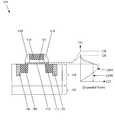
- FIG. 1is a schematic (unscaled) cross-sectional view that depicts a FET in accordance with an embodiment of the invention
- FIGS. 1A and 1Bare schematic (unscaled) views that depict FETs in accordance with an embodiment of the invention.
- FIG. 2is a schematic that depicts a VCO in accordance with an embodiment of the invention
- FIG. 3is a schematic that depicts an alternative VCO design
- FIG. 4is a schematic that depicts a LNA in accordance with an embodiment of the invention.
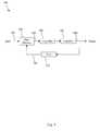
- FIG. 5is a block diagram that depicts a PLL structure
- FIG. 6is a schematic that depicts a PLL in accordance with an embodiment of the invention.
- the inventionmay be embodied in a circuit, such as, for example, a voltage controlled oscillator, low noise amplifier, or a phase locked loop, for processing an RF signal.
- the circuitincludes at least one FET fabricated in a semiconductor a substrate that has at least one planarized layer and one or more strained material layers disposed on the planarized layer. Consequently, the FET, and the circuit, exhibit improved performance, particularly at high signal frequencies.
- the strained material layersmay be characterized by at least one diffusion impurity gradient that has a value that is substantially equal to zero in a particular area of the strained layer.
- Mobility enhancementcan be incorporated into a MOS device by disposing a compositionally graded buffer layer between a SiGe film and the Si substrate. The grading spreads the lattice mismatch within the buffer over a distance, thereby minimizing the number of lattice dislocations reaching the surface on which the film is disposed, and thus providing a method for growing high-quality relaxed SiGe films on Si.
- a Si film having a thicknessis grown on the relaxed SiGe film. Since the lattice constant of SiGe is larger than that of Si, the Si film is under biaxial tension, causing the carriers to exhibit strain-enhanced mobilities.
- strained Si devicesUnlike many GaAs high mobility technologies, strained Si devices generally can be fabricated with standard Si CMOS processing methods and tools. This compatibility generally allows for performance enhancement with minimal additional capital expenditures. The technology is also scalable and thus can be implemented in both long and short channel devices. Furthermore, if desired, strained Si can be incorporated with Si-on-insulator (“SOI”) technology in order to provide ultra-high speed and low power circuits. In summary, since strained Si technology is similar to bulk Si technology, it is not exclusive to other performance enhancing methods. Consequently, strained Si is well-suited to improve the performance of CMOS-based microwave circuits.
- SOISi-on-insulator
- the strained Si material systemcan improve microwave circuit performance several ways.
- Example categoriesinclude:
- Enhanced mobilitylowers the minimum noise figure on buried channel or surface channel devices. This is applicable to, for example, LNAs, VCOs, and PLLs.
- Substrate planarization and re-growthfacilitates photolithography and fabrication of surface or buried channel strained Si layer devices on substrates containing up to, for example, 30% Ge.
- Substrate planarization and re-growth for higher Ge concentrationenables the photolithographically defined, higher performance modulation doped FETs (“MODFETs”) for RF circuits (by virtue of increased hetero-confinement).
- MODFETsmodulation doped FETs
- a digital componentmay be integrated easily with the RF circuit.
- a high quality oxidemay be grown for varactors having a high Q factor.
- a Si channel in a FETis placed under biaxial tension by the underlying, larger-lattice-constant SiGe layer. This strain causes the conduction band to split into two-fold and four-fold degenerate bands. The two-fold band is preferentially occupied since it sits at a lower energy. The energy separation between the bands is approximately:
- Equation (1)shows that the band splitting increases as the Ge content increases. This splitting causes mobility enhancement (compared to unstrained material) typically by two mechanisms. First, the two-fold band has a lower effective mass, and thus higher mobility than the four-fold band. Therefore, as the higher mobility band becomes energetically preferred, the average carrier mobility increases. Second, since the carriers are occupying two orbitals instead of six, inter-valley phonon scattering is reduced, further enhancing the carrier mobility.
- the electron mobility enhancement at high fieldsis approximately 1.75 that of unstrained material, while the hole mobility enhancement is generally negligible.
- the electron mobility enhancementimproves slightly to 1.8 and the hole mobility enhancement rises to about 1.4.
- the band splittingis large enough that almost all of the carriers occupy the high mobility band.
- mobility enhancement as a function of Ge concentrationsaturates above about 30% Ge. Because of the low hole mobility, higher mobility, buried P-channel MOSFETs may offer an improved alternative.
- FETs fabricated using one or more strained Si layershave, for a given source-drain bias, greater drain current compared to FETs fabricated using unstrained Si layers.
- FET transconductanceis defined by: g m ⁇ ⁇ I D ⁇ V G ⁇ V D ( Equation ⁇ ⁇ 2 )
- I Dis the drain current
- V Gis the gate bias voltage
- V Dis the source-drain bias
- This example MOSFET structurehas, at about 100 mV source-drain bias, a transconductance approximately twice that of a 0.8 micron n-channel MOSFET fabricated without strained Si operating at the same bias point. At a source-drain bias of about 2.5 V, the FET with the strained Si has a transconductance approximately 1.4 that of the FET lacking the strained Si.
- C OXis the FET gate capacitance. Since, for example, having a strained Si surface layer can double the transconductance, the cutoff frequency correspondingly doubles for a range of gate biases when compared to the FET without the strained Si.
- the noise figure at both high and low frequenciesis a parameter that can affect the performance of RF and microwave circuits.
- Noisegenerally includes two components: flicker (“l/f”) noise and “white noise” (noise that is generally independent of frequency).
- flicker noisedominates, typically affecting the quality of circuits such as VCOs or PLLs.
- white noisedominates and typically affects the noise figure of LNAs.
- the tunneling probability (“P”)may be expressed as being exponentially dependent on the product of the barrier height (“ ⁇ E”) and transverse effective mass “m t *” (perpendicular to the oxide), that is:
- Equation (4)shows that the probability of (heavy) holes tunneling into traps in the oxide is significantly lower compared to electrons. Consequently, there is typically a reduction in l/f noise in p-channel MOSFETs compared to n-channel MOSFETs, potentially as much as at least one order of magnitude. The reduced mobility of the holes relative to electrons further reduces the l/f noise component.
- the electron tunnelinggenerally occurs along the axes of the constant energy surfaces, i.e., longitudinally along the symmetry axes. Accordingly, the tunneling effective mass for electrons is the longitudinal effective mass, “m l *”, which is equal to 0.98m 0 . This is greater than the transverse effective mass for electrons (0.19m 0 ), which applies in the case of tunneling in unstrained (i.e., bulk) Si.
- the oxide-Si potential barrier height for electrons in strained Siis approximately 2.5 eV and, for holes, it is approximately 5.0 eV. Multiplying each of these terms by the appropriate effective mass (0.98m 0 and 0.49m 0 , respectively) yields about the same value. Consequently, the probability of electrons tunneling into traps within the oxide will be the same in a strained Si device as that for holes in a bulk Si device. Therefore, the l/f noise component in strained surface n-channel MOSFETs approaches that of p-channel MOSFETs, thereby offering substantial improvement over n-channel MOSFETs fabricated in unstrained Si.
- K fis a fitting factor.
- K f , R source , and R gatetypically vary depending on the fabrication process and parasitic capacitance values.
- the cutoff frequencyis proportional to the transconductance, so increasing the latter will improve (decrease) the minimum noise figure of the device.
- equations (3) and (5)the effect of increased transconductance and cutoff frequency will affect NF min by a value corresponding to gm ⁇ 1 ⁇ 2 .
- Table 1shows some typical values for the mobility enhancement, transconductance, cutoff frequency, and minimum noise figure for various strained Si configurations (Ge percentages shown), normalized to bulk Si values: TABLE 1 Trans- Minimum Material Mobility conductance Cutoff Noise Configuration Enhancement (Gain) Frequency Figure 20% NMOS 1.75 1.75 1.75 0.76 30% NMOS 1.8 1.8 1.8 0.75 20% PMOS 1 1 1 1 30% PMOS 1.4 1.4 1.4 0.85
- the mobility enhancementleads to improvement in transconductance (i.e., gain) and cutoff frequency.
- the enhancement in noise figurecan be difficult to predict, since the device geometry and process affect the values of parasitic contact resistances. Nevertheless, the reduction in the value of g m ⁇ 1 ⁇ 2 typically results in a reduction in the noise figure for LNAs that include strained Si MOSFETs.
- the carrier mobility in a strained surface layer MOSFETcan be improved by “burying” the strained layer.
- a SiGe “cap” layerhaving a thickness of about thirty to two hundred Angstroms is deposited on the strained layer (typically Si).
- An oxidei.e., gate dielectric
- the gate dielectric layeris spatially separated (by the cap layer) from the active device channel (i.e., the strained layer).
- the corresponding conduction band offsetallows two-dimensional carrier confinement within the strained Si quantum well.
- the value of the electron mobility in such buried strained Si layerscan reach 2900 cm 2 V ⁇ 1 s ⁇ 1 . This is a substantial increase over the typical 600 cm 2 V ⁇ 1 s ⁇ 1 electron mobility in bulk Si MOSFETs.
- the thickness of the oxide and cap layergenerally affects the high frequency performance of the FET.
- Table 2shows some typical values for mobility enhancement, transconductance, cutoff frequency, and minimum noise figure (all normalized to bulk Si values) for various strained Si n-channel MOSFET configurations having different oxide and cap layer thicknesses: TABLE 2 Equivalent Oxide Cap Layer Oxide Trans- Minimum Thickness Thickness Thickness Mobility conductance Cutoff Noise [Angstroms] [Angstroms] [Angstroms] Enhancement (Gain) Frequency Figure 50 50 66.7 4.3 3.2 0.56 50 100 83.3 4.3 2.5 2.5 0.63 30 50 46.7 4.3 2.8 2.8 0.59 30 100 63.3 4.3 2.0 2.0 0.71 15 50 31.7 4.3 2.0 2.0 0.71 15 100 48.3 4.3 1.3 1.3 0.87
- ⁇ oxand “ ⁇ cap ” are the permittivities of the oxide and cap layer, respectively.
- the spatial separation of charge carriers from the oxide interface by virtue of the cap layeralso decreases l/f noise, typically by about an order of magnitude.
- l/f noisetypically by about an order of magnitude.
- p-channel MOSFETs fabricated on buried channel pseudomorphic strained SiGe alloy layersIn these devices, the mobility is increased relative to bulk Si by a factor of about 1.5.
- the l/f noiseis an order of magnitude lower when compared with conventional p-channel MOSFETs, the implication is that the spatial separation of charges from the oxide interface dominates the magnitude of the l/f noise. Consequently, spatial separation of carriers from the oxide interface in a buried strained layer structures further improves the l/f noise component.
- a FET 100is fabricated in a semiconductor substrate 102 , which may be Si, SiGe, or other compounds such as, for example, GaAs or InP.
- the substrate 102can be multi-layered, and it can include relaxed SiGe disposed on compositionally graded SiGe, or relaxed SiGe disposed on Si. One or more of these layers may be planarized, typically by chemical mechanical polishing (“CMP”).
- CMPchemical mechanical polishing
- the substrate 102may also include a buried insulating layer, such as SiO 2 or Si 3 N 4 . The buried insulating layer may also be doped.
- an isolation well 104Disposed on the substrate 102 is an isolation well 104 , typically including an oxide. Within the isolation well 104 are isolation trenches 106 . A source region 108 and a drain region 112 are typically formed by ion implantation. A FET channel 110 , which can have either n-type or p-type conductivity, is formed from one or more strained layers.
- the strained layerscan include one or more layers of Si, Ge, or SiGe.
- the “strain” in the strained layersmay be compressive or tensile, and it may be induced by lattice mismatch with respect to an adjacent layer. Alternatively, the strain may be induced mechanically by, for example, the deposition of overlayers, such as Si 3 N 4 .
- Another way to induce mechanical strainis to create underlying voids by, for example, implantation of one or more gases followed by annealing. Both of these approaches induce strain in the underlying substrate 102 , in turn causing strain in the channel 110 .
- a gate dielectric 114Disposed on at least part of the channel 110 is a gate dielectric 114 , such as, for example, SiO 2 , Si 3 N 4 , or any other material with a dielectric constant greater than that of SiO 2 (e.g., HfO 2 , HfSiON).
- the gate dielectric 114is typically twelve to one hundred Angstroms thick, and it can include a stacked structure (e.g., thin SiO 2 capped with another material having a high dielectric constant).
- the gate electrode 116Disposed on the gate dielectric 114 is the gate electrode 116 .
- the gate electrode 116 materialcan include doped or undoped polysilicon, doped or undoped poly-SiGe, or metal.
- Disposed about the gate electrode 116are the transistor spacers 118 .
- the transistor spacers 118are typically formed by depositing a dielectric material, which may be the same material as the gate dielectric 114 , followed by anisotropic etching.
- One way to improve the overall performance of the FET 100is to employ an interdigitated, or “comb,” structure, typically by connecting several FETs 100 in parallel, as depicted in FIGS. 1A and 1B.
- a single source contact 108 A and a single drain contact 112 Aare connected to the source region 108 and drain region 112 , respectively, on each device.
- Each FET 100uses the same gate electrode 116 . This configuration typically reduces the resistance of the gate electrode 116 , thereby reducing its time constant and improving frequency response.
- the example interdigitated structure shown in FIG. 1Aincludes several separate source and drain regions 108 , 112 with the common gate electrode 116 placed substantially between them.
- Single source and drain contacts 108 A, 112 Aare connected to each source region 108 and drain region 112 , respectively, typically at contact locations 130 , by bridging the gate electrode 116 .
- FIG. 1BAnother example of an interdigitated structure is shown in FIG. 1B and includes parallel FETs 100 that share a single, elongated source region 108 and a single, elongated drain region 112 . These elongated regions are offset relative to each other.
- the gate electrode 116is disposed, typically in a serpentine pattern, substantially within the area defined by the offset. Overlaying the gate electrode 116 are several bridging contacts, typically at contact locations 130 , that help reduce its resistance, as discussed above.
- the addition of the various material layers described abovemay be accomplished using any conventional deposition method (e.g., chemical vapor deposition (“CVD”) or molecular beam epitaxy (“MBE”)), and the method may be plasma-assisted.
- CVDchemical vapor deposition
- MBEmolecular beam epitaxy
- a region that supplies excess carriers to the channel 110may be disposed substantially adjacent to the latter.
- This regiongenerally includes a p- or n-type impurity (i.e., dopant) that acts as a source of the excess carriers (holes or electrons, respectively).
- the presence of these excess carrierstypically improves FET performance.
- the impuritycan also be introduced after the addition of the layers using, for example, ion implantation.
- An impurity gradient 120 A, 120 B(collectively, “ 120 ”) characterizes the channel 110 and the substrate 102 , as well as the isolation well 104 .
- Axis 122represents the impurity concentration, typically in units of cm ⁇ 3 .
- Axis 124corresponds to the location in the FET 100 .
- Axis 124is aligned with the FET 100 to illustrate a typical impurity profile, meaning that the impurity concentration at any point in the F 100 can be ascertained as a function of location.
- the impurity gradient 120is shown in FIG. 1 in an expanded view that, for clarity, differs in scale compared to the remainder of (unscaled) FIG. 1.
- a distal zone of the channel 110is the furthest part of the channel 110 that is located away from the substrate 102 .
- the distal zonetypically includes at least about fifty Angstroms of the furthest part of the channel 110 . That is, the distal zone is at least about fifty Angstroms thick.
- the distal zonecorresponds to that portion of the impurity gradient 120 between boundaries 126 , 128 (expanded for clarity).
- the impurity gradient 120has a value substantially equal to zero.
- impurity gradient 120can also have a value substantially equal to zero before reaching the boundary 126 .
- impurity gradient 120 Amay describe a profile of a p-type (e.g., boron) or n-type (e.g., phosphorous or arsenic) dopant introduced in the substrate 102 .
- impurity gradient 120 Bmay, for example, describe a substantially constant concentration of Ge, or Si, or both, in the substrate 102 that takes on a desired value (e.g., a reduced value) in the channel 110 .
- the impurity gradient 120may describe the concentration of any species in the substrate 102 , including the substrate species itself, at any point in the FET 100 .
- an alternative embodimentincludes disposing a relaxed SiGe “cap” layer between the channel 110 and the gate dielectric 114 .
- the resulting structureis termed a buried strained channel FET, and it has many performance advantages over the surface strained channel FET depicted in FIG. 1.
- FIG. 2is schematic that depicts a VCO 200 in accordance with an embodiment of the invention.
- the VCO 200includes several FETs (denoted by reference designators beginning with “M”) and varactor diodes (denoted by reference designators beginning with “Q”). Also included are impedance elements (see reference designators beginning with “R”), that are resistive at the frequency or frequencies of interest.
- VCO 200output 202 has a frequency that is a function of bias voltage 204 .
- the connection between the gate of FET M 2 and drain of FET M 1provides positive feedback to sustain oscillation.
- FETs M 3 and M 4are part of the biasing network, and inductor L and capacitor C 1 form a tuned L-C circuit.
- Varactor diodes Q 1 through Q 3are typically bipolar structures, meaning a single-chip VCO may be fabricated using a BiCMOS process.
- FETs M 1 through M 4are fabricated with channels that include one or more strained channel layers disposed on one or more planarized substrate layers.
- the channelsmay be buried below the device surface, or may be surface channels, both as described above. Consequently, the FETs M 1 through M 4 exhibit improved noise figures, thereby reducing the overall phase noise of the entire VCO 200 .
- VCO 300includes an input stage based on a differential amplifier (generally, FETs Q 35 through Q 38 ).
- the VCO 300also includes a multivibrator circuit (generally, FETs Q 23 and Q 24 ) that has a free running frequency that is inversely proportional to the capacitance C.
- FETsthat have one or more strained layers, the overall performance of VCO 300 is enhanced.
- an LNA 400is fabricated using a FET 4 -M 1 that includes one or more strained channel layers disposed on one or more planarized substrate layers.
- LNA 400includes a biasing network Rbias.
- Inductive elements LG, LSprovide input matching.
- the overall noise figure for the LNA 400 as a function of frequency (“ ⁇ ”)is: NF LNA ⁇ 1 + 8 ⁇ ⁇ 2 ⁇ C gs 2 ⁇ R S 3 ⁇ g m ( Equation ⁇ ⁇ 7 )
- the noise figure of the LNA 400decreases.
- FETs fabricated using one or more strained Si layershave, for a given source-drain bias, greater drain current, and therefore greater transconductance, compared to conventional FETs. Consequently, LNA 400 has improved noise performance compared to LNAs fabricated using conventional FETs.
- FIG. 5is a block diagram that shows a basic PLL 500 .
- a VCO 516oscillates at that frequency.
- a phase detector 504produces a signal 506 that is proportional to the phase difference between the input signal 502 and the VCO output signal 508 .
- the signal 506is passed through a loop filter 510 , then to amplifier 512 , and becomes output signal 514 .
- Output signal 514is also fed back to control the VCO 516 .
- VCOs 200 , 300depicted in FIGS. 2 and 3, respectively, are used in place of the VCO 516 .
- LNA 400is used as the amplifier 512 .
- the improved performance of VCOs 200 , 300 , and LNA 400results in a PLL 500 that exhibits similar operational performance enhancements (e.g., improved transconductance, noise figure, etc.).
- FIG. 6depicts an alternative PLL design 600 .
- PLL design 600uses FETs fabricated with channels that include one or more strained channel layers disposed on one or more planarized substrate layers in many, if not all, instances in the PLL 500 . This further enhances the overall operational performance of the PLL 500 .
Landscapes
- Insulated Gate Type Field-Effect Transistor (AREA)
- Metal-Oxide And Bipolar Metal-Oxide Semiconductor Integrated Circuits (AREA)
- Bipolar Integrated Circuits (AREA)
- Inductance-Capacitance Distribution Constants And Capacitance-Resistance Oscillators (AREA)
- Stabilization Of Oscillater, Synchronisation, Frequency Synthesizers (AREA)
Abstract
Description
- This application claims priority to and the benefit of, and incorporates herein by reference, in its entirety, provisional U.S. patent application Serial No. 60/324,329, filed Sep. 24, 2001.[0001]
- The present invention relates generally to circuits that process radio frequency (hereinafter, “RF”) and microwave signals and, more specifically, to RF circuits that contain transistors, including field effect transistors (hereinafter, “FETs” or “MOSFETs”) that incorporate one or more strained material layers.[0002]
- Continuous improvements in semiconductor process technology have extended the capability of silicon (“Si”) CMOS devices into the RF and microwave domain. Improvements resulting in, for example, smaller FET gate lengths have increased the maximum frequency of operation. There has been long-standing interest in increasing the frequency capability of Si for many reasons, including the generally lower cost of Si-based devices compared to III-V devices, such as, for example, those fabricated from gallium arsenide (“GaAs”) and indium phosphide (“InP”). Furthermore, given the overall maturity of Si process technology, mixed signal devices (i.e., devices that process both analog and digital signals on the same semiconductor chip), are generally more easily fabricated in Si than in other materials. Other advantages of Si include greater surface smoothness and a high thermal conductivity (approximately three times that of GaAs). Si also has a high dielectric constant that is generally unaffected by variations in temperature, or frequency, or both.[0003]
- On the other hand, the intrinsic peak mobility of electrons in Si is approximately 600 cm[0004]2V−1s−1. This is lower than the electron mobility of 8500 cm2V−1s−1in GaAs. Accordingly, for Si-based devices to have performance (per unit gate width) that is substantially equivalent to GaAs-based devices, Si gate lengths must be scaled downward significantly. For example, NMOS devices have been demonstrated that have cutoff frequencies between 120 GHz and 150 GHz, with effective electrical gate lengths on the order of 0.09 micrometer.
- A problem with such significant downward scaling of gate length is that doing so affects the noise performance of the resulting device. Although long channel devices have been demonstrated that have a noise figure of approximately 1-2 dB, as gate lengths decrease, short channel (e.g., “shot”) noise typically begins to degrade device performance. Adding one or more bipolar structures to the CMOS semiconductor chip (resulting in a “BiCMOS” design) can circumvent this problem. Nevertheless, a BiCMOS structure adds several steps to the CMOS fabrication process, thereby increasing production complexity and cost.[0005]
- The Si substrates used in the fabrication of RF devices typically have a lower resistivity compared to GaAs substrates. This generally causes greater signal losses in Si compared to GaAs. This, in turn, typically results in increased power consumption in the GHz regime for Si-based devices, and lower quality (“Q”) factors for passive Si-based components, the latter of which degrades the noise performance.[0006]
- RF circuits, such as voltage controlled oscillators (“VCOs”), low noise amplifiers (“LNAs”), and phase locked loops (“PLLs”), typically include one or more transistors. When operated at high frequency, these circuits can suffer from poor performance like that described above due, at least in part, to their use of one or more conventional transistors in the overall circuit designs. Converting such designs to GaAs or BiCMOS can be problematic, particularly when a circuit is monolithic (i.e., when the most or all of the circuit is contained on one semiconductor chip). The increase in cost and complexity of such a conversion can make it impractical or impossible.[0007]
- From the foregoing, it is apparent that there is still a need for a way to improve the performance of RF circuits, particularly at high frequencies, while avoiding changes to the circuit designs or fabrication sequences that can increase cost and complexity.[0008]
- The present invention provides circuits for processing RF signals that exhibit improved performance without requiring significant changes to design or fabrication. This is accomplished by including in the circuits devices (either active, or passive, or both) having enhanced material properties, such as, for example, increased electron and hole mobilities. Consequently, these devices exhibit superior performance that, in turn, influences overall circuit operation.[0009]
- The invention features a circuit that includes one or more FETs to which an RF signal is applied. In different embodiments, the circuit can include one or more of a voltage controlled oscillator, a low noise amplifier, or phase locked loop. The FETs are fabricated in a semiconductor substrate that includes at least one planarized layer. The channel regions of these FETs include one or more strained material layers disposed on a planarized layer.[0010]
- In certain embodiments, the semiconductor substrate can include Si, SiGe, or any combination of these materials. It can also be multi-layered. In this latter case, the layers can include relaxed SiGe disposed on compositionally graded SiGe. The layers can also include relaxed SiGe disposed on Si. One or more buried insulating layers may be included as well.[0011]
- In other embodiments, the strained layer can include Si, Ge, SiGe, or any combination of these materials. At least about fifty Angstroms of the strained layer farthest from the planarized layer defines a distal zone where an impurity gradient (describing the concentration of one or more impurities (i.e., dopants) as a function of location in the device) has a value that is substantially equal to zero.[0012]
- Other aspects and advantages of the present invention will become apparent from the following detailed description, taken in conjunction with the accompanying drawings, illustrating the principles of the invention by way of example only.[0013]
- The foregoing and other objects, features, and advantages of the present invention, as well as the invention itself, will be more fully understood from the following description of various embodiments, when read together with the accompanying drawings, in which:[0014]
- FIG. 1 is a schematic (unscaled) cross-sectional view that depicts a FET in accordance with an embodiment of the invention;[0015]
- FIGS. 1A and 1B are schematic (unscaled) views that depict FETs in accordance with an embodiment of the invention;[0016]
- FIG. 2 is a schematic that depicts a VCO in accordance with an embodiment of the invention;[0017]
- FIG. 3 is a schematic that depicts an alternative VCO design;[0018]
- FIG. 4 is a schematic that depicts a LNA in accordance with an embodiment of the invention;[0019]
- FIG. 5 is a block diagram that depicts a PLL structure; and[0020]
- FIG. 6 is a schematic that depicts a PLL in accordance with an embodiment of the invention.[0021]
- As shown in the drawings for the purposes of illustration, the invention may be embodied in a circuit, such as, for example, a voltage controlled oscillator, low noise amplifier, or a phase locked loop, for processing an RF signal. The circuit includes at least one FET fabricated in a semiconductor a substrate that has at least one planarized layer and one or more strained material layers disposed on the planarized layer. Consequently, the FET, and the circuit, exhibit improved performance, particularly at high signal frequencies. In some embodiments, the strained material layers may be characterized by at least one diffusion impurity gradient that has a value that is substantially equal to zero in a particular area of the strained layer.[0022]
- Technical Background[0023]
- When Si is placed under tension, the degeneracy of the conduction band splits, forcing two valleys to be occupied instead of six. Consequently, the in-plane mobility is increased, reaching a value as high as 2900 cm[0024]2V−1s−1in buried channel devices for electron densities of 1011-1012cm−2. Mobility enhancement can be incorporated into a MOS device by disposing a compositionally graded buffer layer between a SiGe film and the Si substrate. The grading spreads the lattice mismatch within the buffer over a distance, thereby minimizing the number of lattice dislocations reaching the surface on which the film is disposed, and thus providing a method for growing high-quality relaxed SiGe films on Si. Typically, a Si film having a thickness is grown on the relaxed SiGe film. Since the lattice constant of SiGe is larger than that of Si, the Si film is under biaxial tension, causing the carriers to exhibit strain-enhanced mobilities.
- Unlike many GaAs high mobility technologies, strained Si devices generally can be fabricated with standard Si CMOS processing methods and tools. This compatibility generally allows for performance enhancement with minimal additional capital expenditures. The technology is also scalable and thus can be implemented in both long and short channel devices. Furthermore, if desired, strained Si can be incorporated with Si-on-insulator (“SOI”) technology in order to provide ultra-high speed and low power circuits. In summary, since strained Si technology is similar to bulk Si technology, it is not exclusive to other performance enhancing methods. Consequently, strained Si is well-suited to improve the performance of CMOS-based microwave circuits.[0025]
- The strained Si material system can improve microwave circuit performance several ways. Example categories include:[0026]
- 1. Circuit and Device Performance—Gain and Noise.[0027]
- a. For RF circuits, the increased mobility improves the device gain compared to CMOS-based designs.[0028]
- b. Enhanced mobility lowers the minimum noise figure on buried channel or surface channel devices. This is applicable to, for example, LNAs, VCOs, and PLLs.[0029]
- c. Use of buried or surface channel devices having improved mobility and increased effective mass perpendicular to the oxide interface (i.e., perpendicular to the direction of current flow) lowers flicker noise, thereby enabling higher performance RF circuits (e.g., VCOs and PLLs).[0030]
- 2. Ease of Fabrication.[0031]
- a. Substrate planarization and re-growth facilitates photolithography and fabrication of surface or buried channel strained Si layer devices on substrates containing up to, for example, 30% Ge.[0032]
- b. Substrate planarization and re-growth for higher Ge concentration enables the photolithographically defined, higher performance modulation doped FETs (“MODFETs”) for RF circuits (by virtue of increased hetero-confinement).[0033]
- c. A digital component may be integrated easily with the RF circuit.[0034]
- 3. Passive Components—Ease of Fabrication, Q-factor and Noise Enhancement.[0035]
- a. Because of implant control for buried channel devices (compared with grown modulation doped structures), there is generally no need to etch away or counter dope one or more epilayers (possibly causing irrecoverable damage, negating the need for additional reconstruction or passivation).[0036]
- b. Because of planarized substrates, there is greater control of defect densities and material quality of the epilayers. There is also greater control (typically by ion implantation) of the substrate contact and doping allowing fabrication of low electrical resistance regions (for ground planes or contacts), and regions of high electrical resistance that enable fabrication of passive components of higher Q and lower noise.[0037]
- c. A high quality oxide may be grown for varactors having a high Q factor.[0038]
- Strained Si Mobility Enhancement[0039]
- Typically, a Si channel in a FET is placed under biaxial tension by the underlying, larger-lattice-constant SiGe layer. This strain causes the conduction band to split into two-fold and four-fold degenerate bands. The two-fold band is preferentially occupied since it sits at a lower energy. The energy separation between the bands is approximately:[0040]
- ΔEstram=0.67x[eV] (Equation 1)
- where “x” is equal to the Ge content in the SiGe layer. Equation (1) shows that the band splitting increases as the Ge content increases. This splitting causes mobility enhancement (compared to unstrained material) typically by two mechanisms. First, the two-fold band has a lower effective mass, and thus higher mobility than the four-fold band. Therefore, as the higher mobility band becomes energetically preferred, the average carrier mobility increases. Second, since the carriers are occupying two orbitals instead of six, inter-valley phonon scattering is reduced, further enhancing the carrier mobility.[0041]
- At a concentration of 20% Ge, the electron mobility enhancement at high fields (0.2˜0.7 MV/cm) is approximately 1.75 that of unstrained material, while the hole mobility enhancement is generally negligible. When the Ge concentration is increased to 30%, the electron mobility enhancement improves slightly to 1.8 and the hole mobility enhancement rises to about 1.4. Above 30% Ge, the band splitting is large enough that almost all of the carriers occupy the high mobility band. As a result, mobility enhancement as a function of Ge concentration saturates above about 30% Ge. Because of the low hole mobility, higher mobility, buried P-channel MOSFETs may offer an improved alternative.[0042]
- Drain Current Enhancement[0043]
- where “I[0045]D” is the drain current, “VG” is the gate bias voltage, and “VD” is the source-drain bias. Accordingly, the greater drain current results in an increased transconductance. Since transistor gain is generally directly proportional to transconductance, the former is also increased by the greater drain current.
- By way of example, consider an n-channel MOSFET fabricated in 0.8 micron process technology using strained Si. The typical process affords low contact resistance. It also minimizes the amount of diffusion of Ge from the buffer layer into the strained material, particularly in at least about fifty Angstroms of the strained material distal to (e.g., farthest from) the buffer layer. This configuration maximizes the mobility increase in the surface strained layer.[0046]
- This example MOSFET structure has, at about 100 mV source-drain bias, a transconductance approximately twice that of a 0.8 micron n-channel MOSFET fabricated without strained Si operating at the same bias point. At a source-drain bias of about 2.5 V, the FET with the strained Si has a transconductance approximately 1.4 that of the FET lacking the strained Si.[0047]
- where “C[0049]OX” is the FET gate capacitance. Since, for example, having a strained Si surface layer can double the transconductance, the cutoff frequency correspondingly doubles for a range of gate biases when compared to the FET without the strained Si.
- Noise Figure Improvement[0050]
- For discrete MOSFET devices, the noise figure at both high and low frequencies is a parameter that can affect the performance of RF and microwave circuits. Noise generally includes two components: flicker (“l/f”) noise and “white noise” (noise that is generally independent of frequency). At low frequencies, flicker noise dominates, typically affecting the quality of circuits such as VCOs or PLLs. At higher frequencies, white noise dominates and typically affects the noise figure of LNAs.[0051]
- With respect to flicker noise, using p-channel MOSFETs in place of n-channel MOSFETs will generally improve the performance of VCOs and PLLs. One reason for this effect is that free charge carriers in the inversion layer at the oxide-semiconductor interface quantum mechanically tunnel into traps within the oxide causing random fluctuations (and hence noise) in the drain current. The tunneling probability (“P”) may be expressed as being exponentially dependent on the product of the barrier height (“ΔE”) and transverse effective mass “m[0052]t*” (perpendicular to the oxide), that is:
- P∝e−ΔEm*t (Equation 4)
- Given that the transverse effective mass for electrons (equal to 0.19m[0053]0, where m0is the electron rest mass) is less than that for (heavy) holes (0.49m0), equation (4) shows that the probability of (heavy) holes tunneling into traps in the oxide is significantly lower compared to electrons. Consequently, there is typically a reduction in l/f noise in p-channel MOSFETs compared to n-channel MOSFETs, potentially as much as at least one order of magnitude. The reduced mobility of the holes relative to electrons further reduces the l/f noise component.
- In strained Si, the electron tunneling generally occurs along the axes of the constant energy surfaces, i.e., longitudinally along the symmetry axes. Accordingly, the tunneling effective mass for electrons is the longitudinal effective mass, “m[0054]l*”, which is equal to 0.98m0. This is greater than the transverse effective mass for electrons (0.19m0), which applies in the case of tunneling in unstrained (i.e., bulk) Si.
- The oxide-Si potential barrier height for electrons in strained Si is approximately 2.5 eV and, for holes, it is approximately 5.0 eV. Multiplying each of these terms by the appropriate effective mass (0.98m[0055]0and 0.49m0, respectively) yields about the same value. Consequently, the probability of electrons tunneling into traps within the oxide will be the same in a strained Si device as that for holes in a bulk Si device. Therefore, the l/f noise component in strained surface n-channel MOSFETs approaches that of p-channel MOSFETs, thereby offering substantial improvement over n-channel MOSFETs fabricated in unstrained Si.
- where “K[0057]f” is a fitting factor. Kf, Rsource, and Rgatetypically vary depending on the fabrication process and parasitic capacitance values. Nevertheless, by equation (3), the cutoff frequency is proportional to the transconductance, so increasing the latter will improve (decrease) the minimum noise figure of the device. In other words, by equations (3) and (5), the effect of increased transconductance and cutoff frequency will affect NFminby a value corresponding to gm−½.
- By way of example, the following table (Table 1) shows some typical values for the mobility enhancement, transconductance, cutoff frequency, and minimum noise figure for various strained Si configurations (Ge percentages shown), normalized to bulk Si values:[0058]
TABLE 1 Trans- Minimum Material Mobility conductance Cutoff Noise Configuration Enhancement (Gain) Frequency Figure 20% NMOS 1.75 1.75 1.75 0.76 30% NMOS 1.8 1.8 1.8 0.75 20% PMOS 1 1 1 1 30% PMOS 1.4 1.4 1.4 0.85 - The mobility enhancement leads to improvement in transconductance (i.e., gain) and cutoff frequency. The enhancement in noise figure can be difficult to predict, since the device geometry and process affect the values of parasitic contact resistances. Nevertheless, the reduction in the value of g[0059]m−½ typically results in a reduction in the noise figure for LNAs that include strained Si MOSFETs.
- Buried Strained Channel Devices[0060]
- The carrier mobility in a strained surface layer MOSFET can be improved by “burying” the strained layer. In this configuration, a SiGe “cap” layer having a thickness of about thirty to two hundred Angstroms is deposited on the strained layer (typically Si). An oxide (i.e., gate dielectric) is then deposited or grown on the cap layer, and the gate electrode is deposited on the oxide. Consequently, and unlike conventional Si MOSFETs, the gate dielectric layer is spatially separated (by the cap layer) from the active device channel (i.e., the strained layer). The corresponding conduction band offset allows two-dimensional carrier confinement within the strained Si quantum well.[0061]
- The value of the electron mobility in such buried strained Si layers can reach 2900 cm[0062]2V−1s−1. This is a substantial increase over the typical 600 cm2V−1s−1electron mobility in bulk Si MOSFETs.
- The thickness of the oxide and cap layer generally affects the high frequency performance of the FET. By way of example, the following table (Table 2) shows some typical values for mobility enhancement, transconductance, cutoff frequency, and minimum noise figure (all normalized to bulk Si values) for various strained Si n-channel MOSFET configurations having different oxide and cap layer thicknesses:[0063]
TABLE 2 Equivalent Oxide Cap Layer Oxide Trans- Minimum Thickness Thickness Thickness Mobility conductance Cutoff Noise [Angstroms] [Angstroms] [Angstroms] Enhancement (Gain) Frequency Figure 50 50 66.7 4.3 3.2 3.2 0.56 50 100 83.3 4.3 2.5 2.5 0.63 30 50 46.7 4.3 2.8 2.8 0.59 30 100 63.3 4.3 2.0 2.0 0.71 15 50 31.7 4.3 2.0 2.0 0.71 15 100 48.3 4.3 1.3 1.3 0.87 - where “ε[0065]ox” and “εcap” are the permittivities of the oxide and cap layer, respectively.
- As Table 2 shows, the values of mobility enhancement, transconductance, cutoff frequency, and minimum noise figure are improved compared to an n-channel MOSFET fabricated in bulk Si.[0066]
- The spatial separation of charge carriers from the oxide interface by virtue of the cap layer also decreases l/f noise, typically by about an order of magnitude. An example of this is seen in p-channel MOSFETs fabricated on buried channel pseudomorphic strained SiGe alloy layers. In these devices, the mobility is increased relative to bulk Si by a factor of about 1.5. Nevertheless, because the l/f noise is an order of magnitude lower when compared with conventional p-channel MOSFETs, the implication is that the spatial separation of charges from the oxide interface dominates the magnitude of the l/f noise. Consequently, spatial separation of carriers from the oxide interface in a buried strained layer structures further improves the l/f noise component.[0067]
- Example Device Structure[0068]
- In one embodiment depicted schematically (i.e., unsealed) in FIG. 1, a[0069]
FET 100 is fabricated in asemiconductor substrate 102, which may be Si, SiGe, or other compounds such as, for example, GaAs or InP. Thesubstrate 102 can be multi-layered, and it can include relaxed SiGe disposed on compositionally graded SiGe, or relaxed SiGe disposed on Si. One or more of these layers may be planarized, typically by chemical mechanical polishing (“CMP”). Thesubstrate 102 may also include a buried insulating layer, such as SiO2or Si3N4. The buried insulating layer may also be doped. - Disposed on the[0070]
substrate 102 is an isolation well104, typically including an oxide. Within the isolation well104 areisolation trenches 106. Asource region 108 and adrain region 112 are typically formed by ion implantation. AFET channel 110, which can have either n-type or p-type conductivity, is formed from one or more strained layers. The strained layers can include one or more layers of Si, Ge, or SiGe. The “strain” in the strained layers may be compressive or tensile, and it may be induced by lattice mismatch with respect to an adjacent layer. Alternatively, the strain may be induced mechanically by, for example, the deposition of overlayers, such as Si3N4. Another way to induce mechanical strain is to create underlying voids by, for example, implantation of one or more gases followed by annealing. Both of these approaches induce strain in theunderlying substrate 102, in turn causing strain in thechannel 110. - Disposed on at least part of the[0071]
channel 110 is agate dielectric 114, such as, for example, SiO2, Si3N4, or any other material with a dielectric constant greater than that of SiO2(e.g., HfO2, HfSiON). Thegate dielectric 114 is typically twelve to one hundred Angstroms thick, and it can include a stacked structure (e.g., thin SiO2capped with another material having a high dielectric constant). - Disposed on the[0072]
gate dielectric 114 is thegate electrode 116. Thegate electrode 116 material can include doped or undoped polysilicon, doped or undoped poly-SiGe, or metal. Disposed about thegate electrode 116 are thetransistor spacers 118. Thetransistor spacers 118 are typically formed by depositing a dielectric material, which may be the same material as thegate dielectric 114, followed by anisotropic etching. - One way to improve the overall performance of the[0073]
FET 100 is to employ an interdigitated, or “comb,” structure, typically by connectingseveral FETs 100 in parallel, as depicted in FIGS. 1A and 1B. In such a configuration, asingle source contact 108A and asingle drain contact 112A are connected to thesource region 108 and drainregion 112, respectively, on each device. EachFET 100 uses thesame gate electrode 116. This configuration typically reduces the resistance of thegate electrode 116, thereby reducing its time constant and improving frequency response. - The example interdigitated structure shown in FIG. 1A includes several separate source and drain[0074]
regions common gate electrode 116 placed substantially between them. Single source anddrain contacts source region 108 and drainregion 112, respectively, typically atcontact locations 130, by bridging thegate electrode 116. Another example of an interdigitated structure is shown in FIG. 1B and includesparallel FETs 100 that share a single,elongated source region 108 and a single,elongated drain region 112. These elongated regions are offset relative to each other. Thegate electrode 116 is disposed, typically in a serpentine pattern, substantially within the area defined by the offset. Overlaying thegate electrode 116 are several bridging contacts, typically atcontact locations 130, that help reduce its resistance, as discussed above. - The addition of the various material layers described above may be accomplished using any conventional deposition method (e.g., chemical vapor deposition (“CVD”) or molecular beam epitaxy (“MBE”)), and the method may be plasma-assisted. When these layers are added, a region that supplies excess carriers to the[0075]
channel 110 may be disposed substantially adjacent to the latter. This region generally includes a p- or n-type impurity (i.e., dopant) that acts as a source of the excess carriers (holes or electrons, respectively). The presence of these excess carriers typically improves FET performance. The impurity can also be introduced after the addition of the layers using, for example, ion implantation. - An[0076]
impurity gradient channel 110 and thesubstrate 102, as well as the isolation well104.Axis 122 represents the impurity concentration, typically in units of cm−3.Axis 124 corresponds to the location in theFET 100.Axis 124 is aligned with theFET 100 to illustrate a typical impurity profile, meaning that the impurity concentration at any point in theF 100 can be ascertained as a function of location. - The impurity gradient[0077]120 is shown in FIG. 1 in an expanded view that, for clarity, differs in scale compared to the remainder of (unscaled) FIG. 1. A distal zone of the
channel 110 is the furthest part of thechannel 110 that is located away from thesubstrate 102. The distal zone typically includes at least about fifty Angstroms of the furthest part of thechannel 110. That is, the distal zone is at least about fifty Angstroms thick. The distal zone corresponds to that portion of the impurity gradient120 betweenboundaries 126,128 (expanded for clarity). Within the distal zone of thechannel 110, the impurity gradient120 has a value substantially equal to zero. The depicted shape of the impurity gradient120 is not intended to be limiting, and the impurity gradient120 can also have a value substantially equal to zero before reaching theboundary 126. For example,impurity gradient 120A may describe a profile of a p-type (e.g., boron) or n-type (e.g., phosphorous or arsenic) dopant introduced in thesubstrate 102. On the other hand,impurity gradient 120B may, for example, describe a substantially constant concentration of Ge, or Si, or both, in thesubstrate 102 that takes on a desired value (e.g., a reduced value) in thechannel 110. Stated differently, the impurity gradient120 may describe the concentration of any species in thesubstrate 102, including the substrate species itself, at any point in theFET 100. - As described above, an alternative embodiment includes disposing a relaxed SiGe “cap” layer between the[0078]
channel 110 and thegate dielectric 114. The resulting structure is termed a buried strained channel FET, and it has many performance advantages over the surface strained channel FET depicted in FIG. 1. - In brief overview, FIG. 2 is schematic that depicts a[0079]
VCO 200 in accordance with an embodiment of the invention. TheVCO 200 includes several FETs (denoted by reference designators beginning with “M”) and varactor diodes (denoted by reference designators beginning with “Q”). Also included are impedance elements (see reference designators beginning with “R”), that are resistive at the frequency or frequencies of interest. - The basic design of a VCO is well known, and additional details are available in, e.g.,[0080]Radio-Frequency Microelectronic Circuits for Telecommunication Applications, Y. Papananos, Kluwer Academic Publishers, 1999, p. 188 et seq., andAnalysis and Design of Analog Integrated Circuits, P. Gray & R. Meyer, John Wiley & Sons, 1984, pp. 628 et seq. Briefly, in
VCO 200,output 202 has a frequency that is a function ofbias voltage 204. The connection between the gate of FET M2 and drain of FET M1 provides positive feedback to sustain oscillation. FETs M3 and M4 are part of the biasing network, and inductor L and capacitor C1 form a tuned L-C circuit. Varactor diodes Q1 through Q3 are typically bipolar structures, meaning a single-chip VCO may be fabricated using a BiCMOS process. - FETs M[0081]1 through M4 are fabricated with channels that include one or more strained channel layers disposed on one or more planarized substrate layers. The channels may be buried below the device surface, or may be surface channels, both as described above. Consequently, the FETs M1 through M4 exhibit improved noise figures, thereby reducing the overall phase noise of the
entire VCO 200. - Other VCO designs that incorporate FETs having the strained layer on planarized layer structure are possible including, for example,[0082]
VCO 300 depicted in FIG. 3. Briefly,VCO 300 includes an input stage based on a differential amplifier (generally, FETs Q35 through Q38). TheVCO 300 also includes a multivibrator circuit (generally, FETs Q23 and Q24) that has a free running frequency that is inversely proportional to the capacitance C. By using FETs that have one or more strained layers, the overall performance ofVCO 300 is enhanced. - In another embodiment depicted in FIG. 4 in simplified form, an[0083]
LNA 400 is fabricated using a FET4-M1 that includes one or more strained channel layers disposed on one or more planarized substrate layers.LNA 400 includes a biasing network Rbias. Inductive elements LG, LS provide input matching. The overall noise figure for theLNA 400 as a function of frequency (“ω”) is:
- Accordingly, as the transconductance increases, the noise figure of the[0084]
LNA 400 decreases. As discussed above in connection with equation (2), FETs fabricated using one or more strained Si layers have, for a given source-drain bias, greater drain current, and therefore greater transconductance, compared to conventional FETs. Consequently,LNA 400 has improved noise performance compared to LNAs fabricated using conventional FETs. - FIG. 5 is a block diagram that shows a[0085]
basic PLL 500. As is well known, when thePLL 500 is “locked” on aninput signal 502 having a particular frequency, aVCO 516 oscillates at that frequency. Aphase detector 504 produces asignal 506 that is proportional to the phase difference between theinput signal 502 and theVCO output signal 508. Thesignal 506 is passed through aloop filter 510, then toamplifier 512, and becomesoutput signal 514.Output signal 514 is also fed back to control theVCO 516. - In various embodiments of the invention,[0086]
alternative VCOs VCO 516. In other embodiments,LNA 400 is used as theamplifier 512. In each case, the improved performance ofVCOs LNA 400, as described above, results in aPLL 500 that exhibits similar operational performance enhancements (e.g., improved transconductance, noise figure, etc.). - FIG. 6 depicts an[0087]
alternative PLL design 600.PLL design 600 uses FETs fabricated with channels that include one or more strained channel layers disposed on one or more planarized substrate layers in many, if not all, instances in thePLL 500. This further enhances the overall operational performance of thePLL 500. - From the foregoing, it will be appreciated that the RF circuits provided by the invention afford improved operational performance. Certain operational problems resulting from the limitations inherent in conventional devices used in conventional circuits are largely eliminated.[0088]
- One skilled in the art will realize the invention may be embodied in other specific forms without departing from the spirit or essential characteristics thereof. The foregoing embodiments are therefore to be considered in all respects illustrative rather than limiting of the invention described herein. Scope of the invention is thus indicated by the appended claims, rather than by the foregoing description, and all changes which come within the meaning and range of equivalency of the claims are therefore intended to be embraced therein.[0089]


Claims (18)
1. A circuit for processing an RF signal comprising at least one FET to which the RF signal is applied, the at least one FET comprising:
a semiconductor substrate including at least one planarized layer;
a channel region including at least one strained channel layer disposed on the at least one planarized layer; and
a gate electrode.
2. The circuit ofclaim 1 wherein the substrate comprises Si.
3. The circuit ofclaim 1 wherein the substrate comprises SiGe.
4. The circuit ofclaim 1 wherein the at least one planarized layer comprises relaxed SiGe disposed on compositionally graded SiGe.
5. The circuit ofclaim 1 wherein the at least one planarized layer comprises relaxed SiGe disposed on Si.
6. The circuit ofclaim 1 wherein the substrate comprises a buried insulating layer.
7. The circuit ofclaim 1 wherein the at least one strained channel layer comprises Si.
8. The circuit ofclaim 1 wherein the at least one strained channel layer comprises Ge.
9. The circuit ofclaim 1 wherein the at least one strained channel layer comprises SiGe.
10. The circuit ofclaim 1 wherein the channel region comprises n-type conductivity.
11. The circuit ofclaim 1 wherein the channel region comprises p-type conductivity.
12. The circuit ofclaim 1 wherein a gate dielectric is disposed substantially between the gate electrode and the channel region.
13. The circuit ofclaim 1 wherein the FET comprises an interdigitated structure.
14. The circuit ofclaim 1 wherein an excess carrier supply region is disposed substantially adjacent to the channel region.
15. The circuit ofclaim 13 wherein the excess carrier supply region is formed at least in part by implantation of at least one impurity.
16. The circuit ofclaim 1 wherein the circuit comprises a voltage controlled oscillator.
17. The circuit ofclaim 1 wherein the circuit comprises a low noise amplifier.
18. The circuit ofclaim 1 wherein the circuit comprises a phase locked loop.
Priority Applications (5)
| Application Number | Priority Date | Filing Date | Title |
|---|---|---|---|
| US10/253,361US6933518B2 (en) | 2001-09-24 | 2002-09-24 | RF circuits including transistors having strained material layers |
| US11/032,413US7709828B2 (en) | 2001-09-24 | 2005-01-10 | RF circuits including transistors having strained material layers |
| US12/767,671US7906776B2 (en) | 2001-09-24 | 2010-04-26 | RF circuits including transistors having strained material layers |
| US13/017,694US8247798B2 (en) | 2001-09-24 | 2011-01-31 | RF circuits including transistors having strained material layers |
| US13/568,944US8809835B2 (en) | 2001-09-24 | 2012-08-07 | RF circuits including transistors having strained material layers |
Applications Claiming Priority (2)
| Application Number | Priority Date | Filing Date | Title |
|---|---|---|---|
| US32432901P | 2001-09-24 | 2001-09-24 | |
| US10/253,361US6933518B2 (en) | 2001-09-24 | 2002-09-24 | RF circuits including transistors having strained material layers |
Related Child Applications (1)
| Application Number | Title | Priority Date | Filing Date |
|---|---|---|---|
| US11/032,413ContinuationUS7709828B2 (en) | 2001-09-24 | 2005-01-10 | RF circuits including transistors having strained material layers |
Publications (2)
| Publication Number | Publication Date |
|---|---|
| US20030102498A1true US20030102498A1 (en) | 2003-06-05 |
| US6933518B2 US6933518B2 (en) | 2005-08-23 |
Family
ID=23263118
Family Applications (5)
| Application Number | Title | Priority Date | Filing Date |
|---|---|---|---|
| US10/253,361Expired - LifetimeUS6933518B2 (en) | 2001-09-24 | 2002-09-24 | RF circuits including transistors having strained material layers |
| US11/032,413Expired - LifetimeUS7709828B2 (en) | 2001-09-24 | 2005-01-10 | RF circuits including transistors having strained material layers |
| US12/767,671Expired - LifetimeUS7906776B2 (en) | 2001-09-24 | 2010-04-26 | RF circuits including transistors having strained material layers |
| US13/017,694Expired - Fee RelatedUS8247798B2 (en) | 2001-09-24 | 2011-01-31 | RF circuits including transistors having strained material layers |
| US13/568,944Expired - LifetimeUS8809835B2 (en) | 2001-09-24 | 2012-08-07 | RF circuits including transistors having strained material layers |
Family Applications After (4)
| Application Number | Title | Priority Date | Filing Date |
|---|---|---|---|
| US11/032,413Expired - LifetimeUS7709828B2 (en) | 2001-09-24 | 2005-01-10 | RF circuits including transistors having strained material layers |
| US12/767,671Expired - LifetimeUS7906776B2 (en) | 2001-09-24 | 2010-04-26 | RF circuits including transistors having strained material layers |
| US13/017,694Expired - Fee RelatedUS8247798B2 (en) | 2001-09-24 | 2011-01-31 | RF circuits including transistors having strained material layers |
| US13/568,944Expired - LifetimeUS8809835B2 (en) | 2001-09-24 | 2012-08-07 | RF circuits including transistors having strained material layers |
Country Status (3)
| Country | Link |
|---|---|
| US (5) | US6933518B2 (en) |
| AU (1) | AU2002341803A1 (en) |
| WO (1) | WO2003028106A2 (en) |
Cited By (35)
| Publication number | Priority date | Publication date | Assignee | Title |
|---|---|---|---|---|
| US20030077867A1 (en)* | 2001-03-02 | 2003-04-24 | Fitzergald Eugene A. | Relaxed silicon germanium platform for high speed CMOS electronics and high speed analog circuits |
| US20030111678A1 (en)* | 2001-12-14 | 2003-06-19 | Luigi Colombo | CVD deposition of M-SION gate dielectrics |
| US20030215990A1 (en)* | 2002-03-14 | 2003-11-20 | Eugene Fitzgerald | Methods for fabricating strained layers on semiconductor substrates |
| US20040000268A1 (en)* | 1998-04-10 | 2004-01-01 | Massachusetts Institute Of Technology | Etch stop layer system |
| US20040040493A1 (en)* | 2002-08-30 | 2004-03-04 | Amberwave Systems Corporation | Reduction of dislocation pile-up formation during relaxed lattice-mismatched epitaxy |
| US6703144B2 (en) | 2000-01-20 | 2004-03-09 | Amberwave Systems Corporation | Heterointegration of materials using deposition and bonding |
| US6724008B2 (en) | 2001-03-02 | 2004-04-20 | Amberwave Systems Corporation | Relaxed silicon germanium platform for high speed CMOS electronics and high speed analog circuits |
| US20040075105A1 (en)* | 2002-08-23 | 2004-04-22 | Amberwave Systems Corporation | Semiconductor heterostructures having reduced dislocation pile-ups and related methods |
| US20040084668A1 (en)* | 2002-07-08 | 2004-05-06 | Amberwave Systems Corporation | Back-biasing to populate strained layer quantum wells |
| US20040097025A1 (en)* | 2000-12-04 | 2004-05-20 | Amberwave Systems Corporation | Method of fabricating CMOS inverter and integrated circuits utilizing strained silicon surface channel mosfets |
| US20040203213A1 (en)* | 2003-03-25 | 2004-10-14 | Yi-Sun Chung | Method for manufacturing an MOS varactor |
| US20050068117A1 (en)* | 2003-09-30 | 2005-03-31 | Gaurab Banerjee | Strained-silicon voltage controlled oscillator (VCO) |
| US6876010B1 (en) | 1997-06-24 | 2005-04-05 | Massachusetts Institute Of Technology | Controlling threading dislocation densities in Ge on Si using graded GeSi layers and planarization |
| US6921914B2 (en) | 2000-08-16 | 2005-07-26 | Massachusetts Institute Of Technology | Process for producing semiconductor article using graded epitaxial growth |
| US6940089B2 (en) | 2001-04-04 | 2005-09-06 | Massachusetts Institute Of Technology | Semiconductor device structure |
| US6995430B2 (en) | 2002-06-07 | 2006-02-07 | Amberwave Systems Corporation | Strained-semiconductor-on-insulator device structures |
| US7074623B2 (en) | 2002-06-07 | 2006-07-11 | Amberwave Systems Corporation | Methods of forming strained-semiconductor-on-insulator finFET device structures |
| US7122449B2 (en) | 2002-06-10 | 2006-10-17 | Amberwave Systems Corporation | Methods of fabricating semiconductor structures having epitaxially grown source and drain elements |
| US7217603B2 (en) | 2002-06-25 | 2007-05-15 | Amberwave Systems Corporation | Methods of forming reacted conductive gate electrodes |
| US7256142B2 (en) | 2001-03-02 | 2007-08-14 | Amberwave Systems Corporation | Relaxed SiGe platform for high speed CMOS electronics and high speed analog circuits |
| US7307273B2 (en) | 2002-06-07 | 2007-12-11 | Amberwave Systems Corporation | Control of strain in device layers by selective relaxation |
| US7332417B2 (en) | 2003-01-27 | 2008-02-19 | Amberwave Systems Corporation | Semiconductor structures with structural homogeneity |
| US7335545B2 (en) | 2002-06-07 | 2008-02-26 | Amberwave Systems Corporation | Control of strain in device layers by prevention of relaxation |
| US7393733B2 (en) | 2004-12-01 | 2008-07-01 | Amberwave Systems Corporation | Methods of forming hybrid fin field-effect transistor structures |
| US20080197384A1 (en)* | 2007-02-21 | 2008-08-21 | Jessica Hartwich | Field Effect Transistor Arrangement |
| US20080237636A1 (en)* | 2007-03-29 | 2008-10-02 | Been-Yih Jin | Transistor having tensile strained channel and system including same |
| US7504704B2 (en) | 2003-03-07 | 2009-03-17 | Amberwave Systems Corporation | Shallow trench isolation process |
| US7615829B2 (en) | 2002-06-07 | 2009-11-10 | Amberwave Systems Corporation | Elevated source and drain elements for strained-channel heterojuntion field-effect transistors |
| US20130077002A1 (en)* | 2011-09-27 | 2013-03-28 | Young-Soo Yoon | Liquid crystal display |
| US8748292B2 (en) | 2002-06-07 | 2014-06-10 | Taiwan Semiconductor Manufacturing Company, Ltd. | Methods of forming strained-semiconductor-on-insulator device structures |
| US8822282B2 (en) | 2001-03-02 | 2014-09-02 | Taiwan Semiconductor Manufacturing Company, Ltd. | Methods of fabricating contact regions for FET incorporating SiGe |
| US20160133758A1 (en)* | 2014-05-08 | 2016-05-12 | Triquint Semiconductor, Inc. | Dual stack varactor |
| US20180226347A1 (en)* | 2017-02-08 | 2018-08-09 | Globalfoundries Inc. | Heterojunction Bipolar Transistors With Stress Material For Improved Mobility |
| US10535784B2 (en) | 2014-05-08 | 2020-01-14 | Qorvo Us, Inc. | Dual stack varactor |
| US10833071B2 (en) | 2014-05-08 | 2020-11-10 | Qorvo Us, Inc. | Dual-series varactor EPI |
Families Citing this family (74)
| Publication number | Priority date | Publication date | Assignee | Title |
|---|---|---|---|---|
| US6831292B2 (en) | 2001-09-21 | 2004-12-14 | Amberwave Systems Corporation | Semiconductor structures employing strained material layers with defined impurity gradients and methods for fabricating same |
| US6933518B2 (en)* | 2001-09-24 | 2005-08-23 | Amberwave Systems Corporation | RF circuits including transistors having strained material layers |
| US20050285140A1 (en)* | 2004-06-23 | 2005-12-29 | Chih-Hsin Ko | Isolation structure for strained channel transistors |
| US7303949B2 (en)* | 2003-10-20 | 2007-12-04 | International Business Machines Corporation | High performance stress-enhanced MOSFETs using Si:C and SiGe epitaxial source/drain and method of manufacture |
| JP4256328B2 (en)* | 2003-12-05 | 2009-04-22 | 株式会社東芝 | Field effect transistor, semiconductor device, and photorelay |
| JP2007535662A (en)* | 2004-04-02 | 2007-12-06 | カミンズ,チモシー | Integrated electronic sensor |
| WO2007036922A1 (en)* | 2005-09-30 | 2007-04-05 | Timothy Cummins | An integrated electronic sensor |
| US8357958B2 (en)* | 2004-04-02 | 2013-01-22 | Silicon Laboratories Inc. | Integrated CMOS porous sensor |
| US20060151787A1 (en)* | 2005-01-12 | 2006-07-13 | International Business Machines Corporation | LOW CONCENTRATION SiGe BUFFER DURING STRAINED Si GROWTH OF SSGOI MATERIAL FOR DOPANT DIFFUSION CONTROL AND DEFECT REDUCTION |
| US8129706B2 (en)* | 2006-05-05 | 2012-03-06 | Macronix International Co., Ltd. | Structures and methods of a bistable resistive random access memory |
| US20080079084A1 (en)* | 2006-09-28 | 2008-04-03 | Micron Technology, Inc. | Enhanced mobility MOSFET devices |
| US8273617B2 (en) | 2009-09-30 | 2012-09-25 | Suvolta, Inc. | Electronic devices and systems, and methods for making and using the same |
| US8421162B2 (en) | 2009-09-30 | 2013-04-16 | Suvolta, Inc. | Advanced transistors with punch through suppression |
| US8530286B2 (en) | 2010-04-12 | 2013-09-10 | Suvolta, Inc. | Low power semiconductor transistor structure and method of fabrication thereof |
| US8569128B2 (en) | 2010-06-21 | 2013-10-29 | Suvolta, Inc. | Semiconductor structure and method of fabrication thereof with mixed metal types |
| US8759872B2 (en) | 2010-06-22 | 2014-06-24 | Suvolta, Inc. | Transistor with threshold voltage set notch and method of fabrication thereof |
| US8377783B2 (en) | 2010-09-30 | 2013-02-19 | Suvolta, Inc. | Method for reducing punch-through in a transistor device |
| US8404551B2 (en) | 2010-12-03 | 2013-03-26 | Suvolta, Inc. | Source/drain extension control for advanced transistors |
| US8461875B1 (en) | 2011-02-18 | 2013-06-11 | Suvolta, Inc. | Digital circuits having improved transistors, and methods therefor |
| US8525271B2 (en) | 2011-03-03 | 2013-09-03 | Suvolta, Inc. | Semiconductor structure with improved channel stack and method for fabrication thereof |
| US8400219B2 (en) | 2011-03-24 | 2013-03-19 | Suvolta, Inc. | Analog circuits having improved transistors, and methods therefor |
| US8748270B1 (en) | 2011-03-30 | 2014-06-10 | Suvolta, Inc. | Process for manufacturing an improved analog transistor |
| US8796048B1 (en) | 2011-05-11 | 2014-08-05 | Suvolta, Inc. | Monitoring and measurement of thin film layers |
| US8999861B1 (en) | 2011-05-11 | 2015-04-07 | Suvolta, Inc. | Semiconductor structure with substitutional boron and method for fabrication thereof |
| US8811068B1 (en) | 2011-05-13 | 2014-08-19 | Suvolta, Inc. | Integrated circuit devices and methods |
| US8569156B1 (en) | 2011-05-16 | 2013-10-29 | Suvolta, Inc. | Reducing or eliminating pre-amorphization in transistor manufacture |
| US8735987B1 (en) | 2011-06-06 | 2014-05-27 | Suvolta, Inc. | CMOS gate stack structures and processes |
| US8995204B2 (en) | 2011-06-23 | 2015-03-31 | Suvolta, Inc. | Circuit devices and methods having adjustable transistor body bias |
| US8629016B1 (en) | 2011-07-26 | 2014-01-14 | Suvolta, Inc. | Multiple transistor types formed in a common epitaxial layer by differential out-diffusion from a doped underlayer |
| US8748986B1 (en) | 2011-08-05 | 2014-06-10 | Suvolta, Inc. | Electronic device with controlled threshold voltage |
| KR101891373B1 (en) | 2011-08-05 | 2018-08-24 | 엠아이이 후지쯔 세미컨덕터 리미티드 | Semiconductor devices having fin structures and fabrication methods thereof |
| US8614128B1 (en) | 2011-08-23 | 2013-12-24 | Suvolta, Inc. | CMOS structures and processes based on selective thinning |
| US8645878B1 (en) | 2011-08-23 | 2014-02-04 | Suvolta, Inc. | Porting a circuit design from a first semiconductor process to a second semiconductor process |
| US8713511B1 (en) | 2011-09-16 | 2014-04-29 | Suvolta, Inc. | Tools and methods for yield-aware semiconductor manufacturing process target generation |
| US9164052B1 (en) | 2011-09-30 | 2015-10-20 | Silicon Laboratories Inc. | Integrated gas sensor |
| US8669131B1 (en) | 2011-09-30 | 2014-03-11 | Silicon Laboratories Inc. | Methods and materials for forming gas sensor structures |
| US8691609B1 (en) | 2011-09-30 | 2014-04-08 | Silicon Laboratories Inc. | Gas sensor materials and methods for preparation thereof |
| US8852513B1 (en) | 2011-09-30 | 2014-10-07 | Silicon Laboratories Inc. | Systems and methods for packaging integrated circuit gas sensor systems |
| US9236466B1 (en) | 2011-10-07 | 2016-01-12 | Mie Fujitsu Semiconductor Limited | Analog circuits having improved insulated gate transistors, and methods therefor |
| US8895327B1 (en) | 2011-12-09 | 2014-11-25 | Suvolta, Inc. | Tipless transistors, short-tip transistors, and methods and circuits therefor |
| US8748258B2 (en) | 2011-12-12 | 2014-06-10 | International Business Machines Corporation | Method and structure for forming on-chip high quality capacitors with ETSOI transistors |
| US8709890B2 (en) | 2011-12-12 | 2014-04-29 | International Business Machines Corporation | Method and structure for forming ETSOI capacitors, diodes, resistors and back gate contacts |
| US8819603B1 (en) | 2011-12-15 | 2014-08-26 | Suvolta, Inc. | Memory circuits and methods of making and designing the same |
| US8883600B1 (en) | 2011-12-22 | 2014-11-11 | Suvolta, Inc. | Transistor having reduced junction leakage and methods of forming thereof |
| US8599623B1 (en) | 2011-12-23 | 2013-12-03 | Suvolta, Inc. | Circuits and methods for measuring circuit elements in an integrated circuit device |
| US8970289B1 (en) | 2012-01-23 | 2015-03-03 | Suvolta, Inc. | Circuits and devices for generating bi-directional body bias voltages, and methods therefor |
| US8877619B1 (en) | 2012-01-23 | 2014-11-04 | Suvolta, Inc. | Process for manufacture of integrated circuits with different channel doping transistor architectures and devices therefrom |
| US9093550B1 (en) | 2012-01-31 | 2015-07-28 | Mie Fujitsu Semiconductor Limited | Integrated circuits having a plurality of high-K metal gate FETs with various combinations of channel foundation structure and gate stack structure and methods of making same |
| US9406567B1 (en) | 2012-02-28 | 2016-08-02 | Mie Fujitsu Semiconductor Limited | Method for fabricating multiple transistor devices on a substrate with varying threshold voltages |
| US8863064B1 (en) | 2012-03-23 | 2014-10-14 | Suvolta, Inc. | SRAM cell layout structure and devices therefrom |
| US9059321B2 (en) | 2012-05-14 | 2015-06-16 | International Business Machines Corporation | Buried channel field-effect transistors |
| US9299698B2 (en) | 2012-06-27 | 2016-03-29 | Mie Fujitsu Semiconductor Limited | Semiconductor structure with multiple transistors having various threshold voltages |
| US8637955B1 (en) | 2012-08-31 | 2014-01-28 | Suvolta, Inc. | Semiconductor structure with reduced junction leakage and method of fabrication thereof |
| US9112057B1 (en) | 2012-09-18 | 2015-08-18 | Mie Fujitsu Semiconductor Limited | Semiconductor devices with dopant migration suppression and method of fabrication thereof |
| US9041126B2 (en) | 2012-09-21 | 2015-05-26 | Mie Fujitsu Semiconductor Limited | Deeply depleted MOS transistors having a screening layer and methods thereof |
| US9431068B2 (en) | 2012-10-31 | 2016-08-30 | Mie Fujitsu Semiconductor Limited | Dynamic random access memory (DRAM) with low variation transistor peripheral circuits |
| US8816754B1 (en) | 2012-11-02 | 2014-08-26 | Suvolta, Inc. | Body bias circuits and methods |
| US9093997B1 (en) | 2012-11-15 | 2015-07-28 | Mie Fujitsu Semiconductor Limited | Slew based process and bias monitors and related methods |
| US9070477B1 (en) | 2012-12-12 | 2015-06-30 | Mie Fujitsu Semiconductor Limited | Bit interleaved low voltage static random access memory (SRAM) and related methods |
| US9112484B1 (en) | 2012-12-20 | 2015-08-18 | Mie Fujitsu Semiconductor Limited | Integrated circuit process and bias monitors and related methods |
| US9268885B1 (en) | 2013-02-28 | 2016-02-23 | Mie Fujitsu Semiconductor Limited | Integrated circuit device methods and models with predicted device metric variations |
| US8994415B1 (en) | 2013-03-01 | 2015-03-31 | Suvolta, Inc. | Multiple VDD clock buffer |
| US8988153B1 (en) | 2013-03-09 | 2015-03-24 | Suvolta, Inc. | Ring oscillator with NMOS or PMOS variation insensitivity |
| US9299801B1 (en) | 2013-03-14 | 2016-03-29 | Mie Fujitsu Semiconductor Limited | Method for fabricating a transistor device with a tuned dopant profile |
| US9449967B1 (en) | 2013-03-15 | 2016-09-20 | Fujitsu Semiconductor Limited | Transistor array structure |
| US9112495B1 (en) | 2013-03-15 | 2015-08-18 | Mie Fujitsu Semiconductor Limited | Integrated circuit device body bias circuits and methods |
| US9478571B1 (en) | 2013-05-24 | 2016-10-25 | Mie Fujitsu Semiconductor Limited | Buried channel deeply depleted channel transistor |
| KR20140142887A (en)* | 2013-06-05 | 2014-12-15 | 에스케이하이닉스 주식회사 | 3 Dimension Semiconductor Device And Method of Manufacturing The same |
| US8976575B1 (en) | 2013-08-29 | 2015-03-10 | Suvolta, Inc. | SRAM performance monitor |
| US11901243B2 (en)* | 2013-11-12 | 2024-02-13 | Skyworks Solutions, Inc. | Methods related to radio-frequency switching devices having improved voltage handling capability |
| US9710006B2 (en) | 2014-07-25 | 2017-07-18 | Mie Fujitsu Semiconductor Limited | Power up body bias circuits and methods |
| US9319013B2 (en) | 2014-08-19 | 2016-04-19 | Mie Fujitsu Semiconductor Limited | Operational amplifier input offset correction with transistor threshold voltage adjustment |
| US9530669B1 (en) | 2015-11-30 | 2016-12-27 | International Business Machines Corporation | Method of making a semiconductor device having a semiconductor material on a relaxed semiconductor including replacing a strained, selective etchable material, with a low density dielectric in a cavity |
| CN107038987B (en)* | 2017-05-23 | 2020-12-22 | 上海和辉光电股份有限公司 | A common gate transistor, pixel circuit, driving method and display |
Citations (94)
| Publication number | Priority date | Publication date | Assignee | Title |
|---|---|---|---|---|
| US516084A (en)* | 1894-03-06 | delaney | ||
| US625175A (en)* | 1899-05-16 | Ironing-board | ||
| US4010045A (en)* | 1973-12-13 | 1977-03-01 | Ruehrwein Robert A | Process for production of III-V compound crystals |
| US4987462A (en)* | 1987-01-06 | 1991-01-22 | Texas Instruments Incorporated | Power MISFET |
| US4990979A (en)* | 1988-05-13 | 1991-02-05 | Eurosil Electronic Gmbh | Non-volatile memory cell |
| US4997776A (en)* | 1989-03-06 | 1991-03-05 | International Business Machines Corp. | Complementary bipolar transistor structure and method for manufacture |
| US5013681A (en)* | 1989-09-29 | 1991-05-07 | The United States Of America As Represented By The Secretary Of The Navy | Method of producing a thin silicon-on-insulator layer |
| US5177583A (en)* | 1990-02-20 | 1993-01-05 | Kabushiki Kaisha Toshiba | Heterojunction bipolar transistor |
| US5202284A (en)* | 1989-12-01 | 1993-04-13 | Hewlett-Packard Company | Selective and non-selective deposition of Si1-x Gex on a Si subsrate that is partially masked with SiO2 |
| US5207864A (en)* | 1991-12-30 | 1993-05-04 | Bell Communications Research | Low-temperature fusion of dissimilar semiconductors |
| US5208182A (en)* | 1991-11-12 | 1993-05-04 | Kopin Corporation | Dislocation density reduction in gallium arsenide on silicon heterostructures |
| US5212110A (en)* | 1992-05-26 | 1993-05-18 | Motorola, Inc. | Method for forming isolation regions in a semiconductor device |
| US5221413A (en)* | 1991-04-24 | 1993-06-22 | At&T Bell Laboratories | Method for making low defect density semiconductor heterostructure and devices made thereby |
| US5241197A (en)* | 1989-01-25 | 1993-08-31 | Hitachi, Ltd. | Transistor provided with strained germanium layer |
| US5285086A (en)* | 1990-08-02 | 1994-02-08 | At&T Bell Laboratories | Semiconductor devices with low dislocation defects |
| US5291439A (en)* | 1991-09-12 | 1994-03-01 | International Business Machines Corporation | Semiconductor memory cell and memory array with inversion layer |
| US5298452A (en)* | 1986-09-12 | 1994-03-29 | International Business Machines Corporation | Method and apparatus for low temperature, low pressure chemical vapor deposition of epitaxial silicon layers |
| US5310451A (en)* | 1993-08-19 | 1994-05-10 | International Business Machines Corporation | Method of forming an ultra-uniform silicon-on-insulator layer |
| US5316958A (en)* | 1990-05-31 | 1994-05-31 | International Business Machines Corporation | Method of dopant enhancement in an epitaxial silicon layer by using germanium |
| US5399522A (en)* | 1993-02-16 | 1995-03-21 | Fujitsu Limited | Method of growing compound semiconductor |
| US5413679A (en)* | 1993-06-30 | 1995-05-09 | The United States Of America As Represented By The Secretary Of The Navy | Method of producing a silicon membrane using a silicon alloy etch stop layer |
| US5426069A (en)* | 1992-04-09 | 1995-06-20 | Dalsa Inc. | Method for making silicon-germanium devices using germanium implantation |
| US5426316A (en)* | 1992-12-21 | 1995-06-20 | International Business Machines Corporation | Triple heterojunction bipolar transistor |
| US5442205A (en)* | 1991-04-24 | 1995-08-15 | At&T Corp. | Semiconductor heterostructure devices with strained semiconductor layers |
| US5484664A (en)* | 1988-04-27 | 1996-01-16 | Fujitsu Limited | Hetero-epitaxially grown compound semiconductor substrate |
| US5523592A (en)* | 1993-02-03 | 1996-06-04 | Hitachi, Ltd. | Semiconductor optical device, manufacturing method for the same, and opto-electronic integrated circuit using the same |
| US5534713A (en)* | 1994-05-20 | 1996-07-09 | International Business Machines Corporation | Complementary metal-oxide semiconductor transistor logic using strained SI/SIGE heterostructure layers |
| US5536361A (en)* | 1992-01-31 | 1996-07-16 | Canon Kabushiki Kaisha | Process for preparing semiconductor substrate by bonding to a metallic surface |
| US5540785A (en)* | 1991-06-28 | 1996-07-30 | International Business Machines Corporation | Fabrication of defect free silicon on an insulating substrate |
| US5596527A (en)* | 1992-12-07 | 1997-01-21 | Nippon Steel Corporation | Electrically alterable n-bit per cell non-volatile memory with reference cells |
| US5617351A (en)* | 1992-03-12 | 1997-04-01 | International Business Machines Corporation | Three-dimensional direct-write EEPROM arrays and fabrication methods |
| US5630905A (en)* | 1995-02-06 | 1997-05-20 | The Regents Of The University Of California | Method of fabricating quantum bridges by selective etching of superlattice structures |
| US5659187A (en)* | 1991-05-31 | 1997-08-19 | International Business Machines Corporation | Low defect density/arbitrary lattice constant heteroepitaxial layers |
| US5714777A (en)* | 1997-02-19 | 1998-02-03 | International Business Machines Corporation | Si/SiGe vertical junction field effect transistor |
| US5728623A (en)* | 1994-03-16 | 1998-03-17 | Nec Corporation | Method of bonding a III-V group compound semiconductor layer on a silicon substrate |
| US5739567A (en)* | 1992-11-02 | 1998-04-14 | Wong; Chun Chiu D. | Highly compact memory device with nonvolatile vertical transistor memory cell |
| US5759898A (en)* | 1993-10-29 | 1998-06-02 | International Business Machines Corporation | Production of substrate for tensilely strained semiconductor |
| US5777364A (en)* | 1992-11-30 | 1998-07-07 | International Business Machines Corporation | Graded channel field effect transistor |
| US5777347A (en)* | 1995-03-07 | 1998-07-07 | Hewlett-Packard Company | Vertical CMOS digital multi-valued restoring logic device |
| US5786612A (en)* | 1995-10-25 | 1998-07-28 | Mitsubishi Denki Kabushiki Kaisha | Semiconductor device comprising trench EEPROM |
| US5786614A (en)* | 1997-04-08 | 1998-07-28 | Taiwan Semiconductor Manufacturing Co., Ltd. | Separated floating gate for EEPROM application |
| US5792679A (en)* | 1993-08-30 | 1998-08-11 | Sharp Microelectronics Technology, Inc. | Method for forming silicon-germanium/Si/silicon dioxide heterostructure using germanium implant |
| US5877070A (en)* | 1997-05-31 | 1999-03-02 | Max-Planck Society | Method for the transfer of thin layers of monocrystalline material to a desirable substrate |
| US5891769A (en)* | 1997-04-07 | 1999-04-06 | Motorola, Inc. | Method for forming a semiconductor device having a heteroepitaxial layer |
| US5906951A (en)* | 1997-04-30 | 1999-05-25 | International Business Machines Corporation | Strained Si/SiGe layers on insulator |
| US5906708A (en)* | 1994-11-10 | 1999-05-25 | Lawrence Semiconductor Research Laboratory, Inc. | Silicon-germanium-carbon compositions in selective etch processes |
| US5912479A (en)* | 1996-07-26 | 1999-06-15 | Sony Corporation | Heterojunction bipolar semiconductor device |
| US6013134A (en)* | 1998-02-18 | 2000-01-11 | International Business Machines Corporation | Advance integrated chemical vapor deposition (AICVD) for semiconductor devices |
| US6033995A (en)* | 1997-09-16 | 2000-03-07 | Trw Inc. | Inverted layer epitaxial liftoff process |
| US6033974A (en)* | 1997-05-12 | 2000-03-07 | Silicon Genesis Corporation | Method for controlled cleaving process |
| US6058044A (en)* | 1997-12-10 | 2000-05-02 | Kabushiki Kaisha Toshiba | Shielded bit line sensing scheme for nonvolatile semiconductor memory |
| US6074919A (en)* | 1999-01-20 | 2000-06-13 | Advanced Micro Devices, Inc. | Method of forming an ultrathin gate dielectric |
| US6096590A (en)* | 1996-07-18 | 2000-08-01 | International Business Machines Corporation | Scalable MOS field effect transistor |
| US6103559A (en)* | 1999-03-30 | 2000-08-15 | Amd, Inc. (Advanced Micro Devices) | Method of making disposable channel masking for both source/drain and LDD implant and subsequent gate fabrication |
| US6107653A (en)* | 1997-06-24 | 2000-08-22 | Massachusetts Institute Of Technology | Controlling threading dislocation densities in Ge on Si using graded GeSi layers and planarization |
| US6111267A (en)* | 1997-05-13 | 2000-08-29 | Siemens Aktiengesellschaft | CMOS integrated circuit including forming doped wells, a layer of intrinsic silicon, a stressed silicon germanium layer where germanium is between 25 and 50%, and another intrinsic silicon layer |
| US6177750B1 (en)* | 1998-07-14 | 2001-01-23 | Reliance Electric Technologies, Llc | Rotating assembly construction for high speed induction motor |
| US6184111B1 (en)* | 1998-06-23 | 2001-02-06 | Silicon Genesis Corporation | Pre-semiconductor process implant and post-process film separation |
| US6191007B1 (en)* | 1997-04-28 | 2001-02-20 | Denso Corporation | Method for manufacturing a semiconductor substrate |
| US6191432B1 (en)* | 1996-09-02 | 2001-02-20 | Kabushiki Kaisha Toshiba | Semiconductor device and memory device |
| US6194722B1 (en)* | 1997-03-28 | 2001-02-27 | Interuniversitair Micro-Elektronica Centrum, Imec, Vzw | Method of fabrication of an infrared radiation detector and infrared detector device |
| US6204529B1 (en)* | 1999-08-27 | 2001-03-20 | Hsing Lan Lung | 8 bit per cell non-volatile semiconductor memory structure utilizing trench technology and dielectric floating gate |
| US6207977B1 (en)* | 1995-06-16 | 2001-03-27 | Interuniversitaire Microelektronica | Vertical MISFET devices |
| US6210988B1 (en)* | 1999-01-15 | 2001-04-03 | The Regents Of The University Of California | Polycrystalline silicon germanium films for forming micro-electromechanical systems |
| US6218677B1 (en)* | 1994-08-15 | 2001-04-17 | Texas Instruments Incorporated | III-V nitride resonant tunneling |
| US6232138B1 (en)* | 1997-12-01 | 2001-05-15 | Massachusetts Institute Of Technology | Relaxed InxGa(1-x)as buffers |
| US6235567B1 (en)* | 1999-08-31 | 2001-05-22 | International Business Machines Corporation | Silicon-germanium bicmos on soi |
| US6242324B1 (en)* | 1999-08-10 | 2001-06-05 | The United States Of America As Represented By The Secretary Of The Navy | Method for fabricating singe crystal materials over CMOS devices |
| US20010003364A1 (en)* | 1998-05-27 | 2001-06-14 | Sony Corporation | Semiconductor and fabrication method thereof |
| US6249022B1 (en)* | 1999-10-22 | 2001-06-19 | United Microelectronics Corp. | Trench flash memory with nitride spacers for electron trapping |
| US6261929B1 (en)* | 2000-02-24 | 2001-07-17 | North Carolina State University | Methods of forming a plurality of semiconductor layers using spaced trench arrays |
| US6266278B1 (en)* | 1999-06-30 | 2001-07-24 | Sandisk Corporation | Dual floating gate EEPROM cell array with steering gates shared adjacent cells |
| US6271551B1 (en)* | 1995-12-15 | 2001-08-07 | U.S. Philips Corporation | Si-Ge CMOS semiconductor device |
| US6271726B1 (en)* | 2000-01-10 | 2001-08-07 | Conexant Systems, Inc. | Wideband, variable gain amplifier |
| US6335546B1 (en)* | 1998-07-31 | 2002-01-01 | Sharp Kabushiki Kaisha | Nitride semiconductor structure, method for producing a nitride semiconductor structure, and light emitting device |
| US6339232B1 (en)* | 1999-09-20 | 2002-01-15 | Kabushika Kaisha Toshiba | Semiconductor device |
| US20020014003A1 (en)* | 1998-05-19 | 2002-02-07 | Fuji Machine Mfg. Co., Ltd. | Method and system for mounting electric components |
| US20020024395A1 (en)* | 2000-08-29 | 2002-02-28 | Terumoto Akatsuka | Voltage controlled oscillator with power amplifier |
| US6368733B1 (en)* | 1998-08-06 | 2002-04-09 | Showa Denko K.K. | ELO semiconductor substrate |
| US6372356B1 (en)* | 1998-06-04 | 2002-04-16 | Xerox Corporation | Compliant substrates for growing lattice mismatched films |
| US20020043660A1 (en)* | 2000-06-27 | 2002-04-18 | Shunpei Yamazaki | Semiconductor device and fabrication method therefor |
| US20020052084A1 (en)* | 2000-05-26 | 2002-05-02 | Fitzgerald Eugene A. | Buried channel strained silicon FET using a supply layer created through ion implantation |
| US6399970B2 (en)* | 1996-09-17 | 2002-06-04 | Matsushita Electric Industrial Co., Ltd. | FET having a Si/SiGeC heterojunction channel |
| US20020068393A1 (en)* | 2000-08-07 | 2002-06-06 | Fitzgerald Eugene A. | Gate technology for strained surface channel and strained buried channel MOSFET devices |
| US6403975B1 (en)* | 1996-04-09 | 2002-06-11 | Max-Planck Gesellschaft Zur Forderung Der Wissenschafteneev | Semiconductor components, in particular photodetectors, light emitting diodes, optical modulators and waveguides with multilayer structures grown on silicon substrates |
| US20020072130A1 (en)* | 2000-08-16 | 2002-06-13 | Zhi-Yuan Cheng | Process for producing semiconductor article using graded expital growth |
| US6407406B1 (en)* | 1998-06-30 | 2002-06-18 | Kabushiki Kaisha Toshiba | Semiconductor device and method of manufacturing the same |
| US20020096717A1 (en)* | 2001-01-25 | 2002-07-25 | International Business Machines Corporation | Transferable device-containing layer for silicon-on-insulator applications |
| US20020100942A1 (en)* | 2000-12-04 | 2002-08-01 | Fitzgerald Eugene A. | CMOS inverter and integrated circuits utilizing strained silicon surface channel MOSFETs |
| US20030003679A1 (en)* | 2001-06-29 | 2003-01-02 | Doyle Brian S. | Creation of high mobility channels in thin-body SOI devices |
| US20030013323A1 (en)* | 2001-06-14 | 2003-01-16 | Richard Hammond | Method of selective removal of SiGe alloys |
| US20030025131A1 (en)* | 2001-08-06 | 2003-02-06 | Massachusetts Institute Of Technology | Formation of planar strained layers |
| US6521041B2 (en)* | 1998-04-10 | 2003-02-18 | Massachusetts Institute Of Technology | Etch stop layer system |
| US20030057439A1 (en)* | 2001-08-09 | 2003-03-27 | Fitzgerald Eugene A. | Dual layer CMOS devices |
Family Cites Families (117)
| Publication number | Priority date | Publication date | Assignee | Title |
|---|---|---|---|---|
| DE3542482A1 (en) | 1985-11-30 | 1987-06-04 | Licentia Gmbh | MODULATION-Doped FIELD EFFECT TRANSISTOR |
| US4849370A (en)* | 1987-12-21 | 1989-07-18 | Texas Instruments Incorporated | Anodizable strain layer for SOI semiconductor structures |
| JPH0794420B2 (en) | 1988-08-30 | 1995-10-11 | 宇部興産株式会社 | Process for producing substituted phenoxyacetaldehyde oximes |
| US5313083A (en)* | 1988-12-16 | 1994-05-17 | Raytheon Company | R.F. switching circuits |
| US5250445A (en) | 1988-12-20 | 1993-10-05 | Texas Instruments Incorporated | Discretionary gettering of semiconductor circuits |
| US5089872A (en)* | 1990-04-27 | 1992-02-18 | North Carolina State University | Selective germanium deposition on silicon and resulting structures |
| US5155571A (en) | 1990-08-06 | 1992-10-13 | The Regents Of The University Of California | Complementary field effect transistors having strained superlattice structure |
| DE4101167A1 (en) | 1991-01-17 | 1992-07-23 | Daimler Benz Ag | ARRANGEMENT AND METHOD FOR PRODUCING COMPLEMENTARY FIELD EFFECT TRANSISTORS |
| JPH04307974A (en) | 1991-04-05 | 1992-10-30 | Sharp Corp | Electrically erasable nonvolatile semiconductor memory device |
| JPH07106446B2 (en) | 1991-05-31 | 1995-11-15 | 株式会社タムラ製作所 | Atmosphere control method for inert gas reflow equipment |
| US5166084A (en) | 1991-09-03 | 1992-11-24 | Motorola, Inc. | Process for fabricating a silicon on insulator field effect transistor |
| FR2681472B1 (en) | 1991-09-18 | 1993-10-29 | Commissariat Energie Atomique | PROCESS FOR PRODUCING THIN FILMS OF SEMICONDUCTOR MATERIAL. |
| JPH05166724A (en) | 1991-12-19 | 1993-07-02 | Fujitsu Ltd | Silicon substrate compound semiconductor device and its manufacture |
| JP3270945B2 (en) | 1992-06-04 | 2002-04-02 | 富士通株式会社 | Heteroepitaxial growth method |
| US5283456A (en)* | 1992-06-17 | 1994-02-01 | International Business Machines Corporation | Vertical gate transistor with low temperature epitaxial channel |
| US5242847A (en)* | 1992-07-27 | 1993-09-07 | North Carolina State University At Raleigh | Selective deposition of doped silion-germanium alloy on semiconductor substrate |
| US5461250A (en) | 1992-08-10 | 1995-10-24 | International Business Machines Corporation | SiGe thin film or SOI MOSFET and method for making the same |
| US5346848A (en) | 1993-06-01 | 1994-09-13 | Motorola, Inc. | Method of bonding silicon and III-V semiconductor materials |
| JPH0750410A (en)* | 1993-08-06 | 1995-02-21 | Hitachi Ltd | Semiconductor crystal laminated body, method for forming the same, and semiconductor device |
| JP2980497B2 (en) | 1993-11-15 | 1999-11-22 | 株式会社東芝 | Method of manufacturing dielectric-isolated bipolar transistor |
| CA2131668C (en)* | 1993-12-23 | 1999-03-02 | Carol Galli | Isolation structure using liquid phase oxide deposition |
| JP3902246B2 (en) | 1994-03-01 | 2007-04-04 | 昭和電工株式会社 | Epitaxial wafer manufacturing method |
| US5479033A (en) | 1994-05-27 | 1995-12-26 | Sandia Corporation | Complementary junction heterostructure field-effect transistor |
| JP3361922B2 (en) | 1994-09-13 | 2003-01-07 | 株式会社東芝 | Semiconductor device |
| US5561302A (en)* | 1994-09-26 | 1996-10-01 | Motorola, Inc. | Enhanced mobility MOSFET device and method |
| US5633202A (en)* | 1994-09-30 | 1997-05-27 | Intel Corporation | High tensile nitride layer |
| US5710450A (en)* | 1994-12-23 | 1998-01-20 | Intel Corporation | Transistor with ultra shallow tip and method of fabrication |
| US5976939A (en)* | 1995-07-03 | 1999-11-02 | Intel Corporation | Low damage doping technique for self-aligned source and drain regions |
| JP4150076B2 (en)* | 1996-03-29 | 2008-09-17 | エヌエックスピー ビー ヴィ | Manufacturing method of semiconductor device |
| US5943560A (en) | 1996-04-19 | 1999-08-24 | National Science Council | Method to fabricate the thin film transistor |
| TW335558B (en) | 1996-09-03 | 1998-07-01 | Ibm | High temperature superconductivity in strained SiSiGe |
| US5847419A (en) | 1996-09-17 | 1998-12-08 | Kabushiki Kaisha Toshiba | Si-SiGe semiconductor device and method of fabricating the same |
| EP0838858B1 (en) | 1996-09-27 | 2002-05-15 | Infineon Technologies AG | CMOS integrated circuit and method of manufacturing the same |
| US6140687A (en) | 1996-11-28 | 2000-10-31 | Matsushita Electric Industrial Co., Ltd. | High frequency ring gate MOSFET |
| US5874329A (en)* | 1996-12-05 | 1999-02-23 | Lsi Logic Corporation | Method for artificially-inducing reverse short-channel effects in deep sub-micron CMOS devices |
| US5808344A (en) | 1996-12-13 | 1998-09-15 | International Business Machines Corporation | Single-transistor logic and CMOS inverters |
| JPH10270685A (en) | 1997-03-27 | 1998-10-09 | Sony Corp | Field-effect transistor and its manufacturing method, semiconductor device and its manufacturing method, logic circuit including the semiconductor device, and semiconductor substrate |
| US6723621B1 (en) | 1997-06-30 | 2004-04-20 | International Business Machines Corporation | Abrupt delta-like doping in Si and SiGe films by UHV-CVD |
| US5936274A (en) | 1997-07-08 | 1999-08-10 | Micron Technology, Inc. | High density flash memory |
| US6160303A (en) | 1997-08-29 | 2000-12-12 | Texas Instruments Incorporated | Monolithic inductor with guard rings |
| US5966622A (en) | 1997-10-08 | 1999-10-12 | Lucent Technologies Inc. | Process for bonding crystalline substrates with different crystal lattices |
| US5963817A (en) | 1997-10-16 | 1999-10-05 | International Business Machines Corporation | Bulk and strained silicon on insulator using local selective oxidation |
| TW388087B (en)* | 1997-11-20 | 2000-04-21 | Winbond Electronics Corp | Method of forming buried-channel P-type metal oxide semiconductor |
| US6154475A (en) | 1997-12-04 | 2000-11-28 | The United States Of America As Represented By The Secretary Of The Air Force | Silicon-based strain-symmetrized GE-SI quantum lasers |
| JP3059145B2 (en) | 1997-12-12 | 2000-07-04 | 松下電子工業株式会社 | Nonvolatile semiconductor memory device and driving method thereof |
| FR2773177B1 (en) | 1997-12-29 | 2000-03-17 | France Telecom | PROCESS FOR OBTAINING A SINGLE-CRYSTAL GERMANIUM OR SILICON LAYER ON A SILICON OR SINGLE-CRYSTAL GERMANIUM SUBSTRATE, RESPECTIVELY, AND MULTILAYER PRODUCTS OBTAINED |
| US6180978B1 (en)* | 1997-12-30 | 2001-01-30 | Texas Instruments Incorporated | Disposable gate/replacement gate MOSFETs for sub-0.1 micron gate length and ultra-shallow junctions |
| US6492694B2 (en)* | 1998-02-27 | 2002-12-10 | Micron Technology, Inc. | Highly conductive composite polysilicon gate for CMOS integrated circuits |
| US6153495A (en) | 1998-03-09 | 2000-11-28 | Intersil Corporation | Advanced methods for making semiconductor devices by low temperature direct bonding |
| JP2000031491A (en) | 1998-07-14 | 2000-01-28 | Hitachi Ltd | Semiconductor device, method of manufacturing semiconductor device, semiconductor substrate, and method of manufacturing semiconductor substrate |
| JP2000124325A (en) | 1998-10-16 | 2000-04-28 | Nec Corp | Semiconductor device and method of manufacturing the same |
| US6329063B2 (en) | 1998-12-11 | 2001-12-11 | Nova Crystals, Inc. | Method for producing high quality heteroepitaxial growth using stress engineering and innovative substrates |
| DE19859429A1 (en) | 1998-12-22 | 2000-06-29 | Daimler Chrysler Ag | Process for the production of epitaxial silicon germanium layers |
| US6130453A (en) | 1999-01-04 | 2000-10-10 | International Business Machines Corporation | Flash memory structure with floating gate in vertical trench |
| DE60042666D1 (en)* | 1999-01-14 | 2009-09-17 | Panasonic Corp | Semiconductor component and method for its production |
| US6162688A (en) | 1999-01-14 | 2000-12-19 | Advanced Micro Devices, Inc. | Method of fabricating a transistor with a dielectric underlayer and device incorporating same |
| US6235568B1 (en)* | 1999-01-22 | 2001-05-22 | Intel Corporation | Semiconductor device having deposited silicon regions and a method of fabrication |
| US20010042503A1 (en) | 1999-02-10 | 2001-11-22 | Lo Yu-Hwa | Method for design of epitaxial layer and substrate structures for high-quality epitaxial growth on lattice-mismatched substrates |
| JP2000243958A (en)* | 1999-02-24 | 2000-09-08 | Toshiba Corp | Semiconductor device and manufacturing method thereof |
| US6133799A (en) | 1999-02-25 | 2000-10-17 | International Business Machines Corporation | Voltage controlled oscillator utilizing threshold voltage control of silicon on insulator MOSFETS |
| US6436801B1 (en)* | 1999-02-26 | 2002-08-20 | Texas Instruments Incorporated | Hafnium nitride gate dielectric |
| US6350993B1 (en) | 1999-03-12 | 2002-02-26 | International Business Machines Corporation | High speed composite p-channel Si/SiGe heterostructure for field effect devices |
| KR100441469B1 (en) | 1999-03-12 | 2004-07-23 | 인터내셔널 비지네스 머신즈 코포레이션 | High speed ge channel heterostructures for field effect devices |
| JP4521542B2 (en) | 1999-03-30 | 2010-08-11 | ルネサスエレクトロニクス株式会社 | Semiconductor device and semiconductor substrate |
| US6251755B1 (en) | 1999-04-22 | 2001-06-26 | International Business Machines Corporation | High resolution dopant/impurity incorporation in semiconductors via a scanned atomic force probe |
| US6281532B1 (en)* | 1999-06-28 | 2001-08-28 | Intel Corporation | Technique to obtain increased channel mobilities in NMOS transistors by gate electrode engineering |
| US6228694B1 (en)* | 1999-06-28 | 2001-05-08 | Intel Corporation | Method of increasing the mobility of MOS transistors by use of localized stress regions |
| US6323108B1 (en) | 1999-07-27 | 2001-11-27 | The United States Of America As Represented By The Secretary Of The Navy | Fabrication ultra-thin bonded semiconductor layers |
| US6876053B1 (en)* | 1999-08-13 | 2005-04-05 | Intel Corporation | Isolation structure configurations for modifying stresses in semiconductor devices |
| US6326667B1 (en)* | 1999-09-09 | 2001-12-04 | Kabushiki Kaisha Toshiba | Semiconductor devices and methods for producing semiconductor devices |
| JP4212228B2 (en) | 1999-09-09 | 2009-01-21 | 株式会社東芝 | Manufacturing method of semiconductor device |
| EP1214735A1 (en) | 1999-09-20 | 2002-06-19 | Amberwave Systems Corporation | Method of producing relaxed silicon germanium layers |
| US6281758B1 (en)* | 1999-09-30 | 2001-08-28 | Conexant Systems, Inc. | Differential LC-VCO, charge pump, and loop filter architecture for improved noise-immunity in integrated phase-locked loops |
| US7391087B2 (en)* | 1999-12-30 | 2008-06-24 | Intel Corporation | MOS transistor structure and method of fabrication |
| JP2003520452A (en) | 2000-01-20 | 2003-07-02 | アンバーウェーブ システムズ コーポレイション | Strained silicon metal oxide semiconductor field effect transistor |
| US6316301B1 (en) | 2000-03-08 | 2001-11-13 | Sun Microsystems, Inc. | Method for sizing PMOS pull-up devices |
| US6483156B1 (en)* | 2000-03-16 | 2002-11-19 | International Business Machines Corporation | Double planar gated SOI MOSFET structure |
| JP3603747B2 (en) | 2000-05-11 | 2004-12-22 | 三菱住友シリコン株式会社 | Method for forming SiGe film, method for manufacturing heterojunction transistor, and heterojunction bipolar transistor |
| JP3528756B2 (en)* | 2000-05-12 | 2004-05-24 | 松下電器産業株式会社 | Semiconductor device |
| AU2001268577A1 (en) | 2000-06-22 | 2002-01-02 | Massachusetts Institute Of Technology | Etch stop layer system |
| KR100522758B1 (en)* | 2000-06-28 | 2005-10-21 | 주식회사 하이닉스반도체 | Method for manufacturing semiconductor device |
| KR100398041B1 (en)* | 2000-06-30 | 2003-09-19 | 주식회사 하이닉스반도체 | Method of forming a epi-channel in a semicondector device |
| US6429061B1 (en) | 2000-07-26 | 2002-08-06 | International Business Machines Corporation | Method to fabricate a strained Si CMOS structure using selective epitaxial deposition of Si after device isolation formation |
| JP2002076334A (en) | 2000-08-30 | 2002-03-15 | Hitachi Ltd | Semiconductor device and manufacturing method thereof |
| US6524935B1 (en) | 2000-09-29 | 2003-02-25 | International Business Machines Corporation | Preparation of strained Si/SiGe on insulator by hydrogen induced layer transfer technique |
| JP3998408B2 (en)* | 2000-09-29 | 2007-10-24 | 株式会社東芝 | Semiconductor device and manufacturing method thereof |
| JP2002164520A (en) | 2000-11-27 | 2002-06-07 | Shin Etsu Handotai Co Ltd | Manufacturing method of semiconductor wafer |
| US7312485B2 (en)* | 2000-11-29 | 2007-12-25 | Intel Corporation | CMOS fabrication process utilizing special transistor orientation |
| US6649480B2 (en) | 2000-12-04 | 2003-11-18 | Amberwave Systems Corporation | Method of fabricating CMOS inverter and integrated circuits utilizing strained silicon surface channel MOSFETs |
| JP2004523103A (en) | 2000-12-04 | 2004-07-29 | アンバーウェーブ システムズ コーポレイション | CMOS inverter circuit using strained silicon surface channel MOSFET |
| US6563152B2 (en)* | 2000-12-29 | 2003-05-13 | Intel Corporation | Technique to obtain high mobility channels in MOS transistors by forming a strain layer on an underside of a channel |
| US6455377B1 (en)* | 2001-01-19 | 2002-09-24 | Chartered Semiconductor Manufacturing Ltd. | Method to form very high mobility vertical channel transistor by selective deposition of SiGe or multi-quantum wells (MQWs) |
| JP2002237590A (en)* | 2001-02-09 | 2002-08-23 | Univ Tohoku | MOS type field effect transistor |
| KR100402381B1 (en)* | 2001-02-09 | 2003-10-17 | 삼성전자주식회사 | Cmos transistor having germanium-contained policrystalline silicon gate and method of forming the same |
| US6830976B2 (en) | 2001-03-02 | 2004-12-14 | Amberwave Systems Corproation | Relaxed silicon germanium platform for high speed CMOS electronics and high speed analog circuits |
| WO2002071488A1 (en) | 2001-03-02 | 2002-09-12 | Amberwave Systems Corporation | Relaxed silicon germanium platform for high speed cmos electronics and high speed analog circuits |
| JP2004531054A (en) | 2001-03-02 | 2004-10-07 | アンバーウェーブ システムズ コーポレイション | Relaxed silicon germanium platform for high speed CMOS electronics and high speed analog circuits |
| US6724008B2 (en)* | 2001-03-02 | 2004-04-20 | Amberwave Systems Corporation | Relaxed silicon germanium platform for high speed CMOS electronics and high speed analog circuits |
| WO2002071491A1 (en) | 2001-03-02 | 2002-09-12 | Amberwave Systems Corporation | Relaxed silicon germanium platform for high speed cmos electronics and high speed analog circuits |
| US6900103B2 (en) | 2001-03-02 | 2005-05-31 | Amberwave Systems Corporation | Relaxed silicon germanium platform for high speed CMOS electronics and high speed analog circuits |
| JP2002289533A (en) | 2001-03-26 | 2002-10-04 | Kentaro Sawano | Method for polishing surface of semiconductor, method for fabricating semiconductor device and semiconductor device |
| US6603156B2 (en) | 2001-03-31 | 2003-08-05 | International Business Machines Corporation | Strained silicon on insulator structures |
| WO2002082514A1 (en) | 2001-04-04 | 2002-10-17 | Massachusetts Institute Of Technology | A method for semiconductor device fabrication |
| US6831292B2 (en)* | 2001-09-21 | 2004-12-14 | Amberwave Systems Corporation | Semiconductor structures employing strained material layers with defined impurity gradients and methods for fabricating same |
| US6933518B2 (en)* | 2001-09-24 | 2005-08-23 | Amberwave Systems Corporation | RF circuits including transistors having strained material layers |
| US6621131B2 (en)* | 2001-11-01 | 2003-09-16 | Intel Corporation | Semiconductor transistor having a stressed channel |
| US6605498B1 (en)* | 2002-03-29 | 2003-08-12 | Intel Corporation | Semiconductor transistor having a backfilled channel material |
| US7473947B2 (en)* | 2002-07-12 | 2009-01-06 | Intel Corporation | Process for ultra-thin body SOI devices that incorporate EPI silicon tips and article made thereby |
| US6812086B2 (en)* | 2002-07-16 | 2004-11-02 | Intel Corporation | Method of making a semiconductor transistor |
| CN1286157C (en)* | 2002-10-10 | 2006-11-22 | 松下电器产业株式会社 | Semiconductor device and method for fabricating the same |
| US6743684B2 (en)* | 2002-10-11 | 2004-06-01 | Texas Instruments Incorporated | Method to produce localized halo for MOS transistor |
| US6703648B1 (en)* | 2002-10-29 | 2004-03-09 | Advanced Micro Devices, Inc. | Strained silicon PMOS having silicon germanium source/drain extensions and method for its fabrication |
| US6657223B1 (en)* | 2002-10-29 | 2003-12-02 | Advanced Micro Devices, Inc. | Strained silicon MOSFET having silicon source/drain regions and method for its fabrication |
| US20040119101A1 (en)* | 2002-12-23 | 2004-06-24 | Gerhard Schrom | Contact layout for MOSFETs under tensile strain |
| US7001837B2 (en)* | 2003-01-17 | 2006-02-21 | Advanced Micro Devices, Inc. | Semiconductor with tensile strained substrate and method of making the same |
| US6921913B2 (en)* | 2003-03-04 | 2005-07-26 | Taiwan Semiconductor Manufacturing Co., Ltd. | Strained-channel transistor structure with lattice-mismatched zone |
| JP4307974B2 (en) | 2003-12-12 | 2009-08-05 | 日本碍子株式会社 | Filter pressure loss measuring device |
- 2002
- 2002-09-24USUS10/253,361patent/US6933518B2/ennot_activeExpired - Lifetime
- 2002-09-24WOPCT/US2002/030226patent/WO2003028106A2/ennot_activeApplication Discontinuation
- 2002-09-24AUAU2002341803Apatent/AU2002341803A1/ennot_activeAbandoned
- 2005
- 2005-01-10USUS11/032,413patent/US7709828B2/ennot_activeExpired - Lifetime
- 2010
- 2010-04-26USUS12/767,671patent/US7906776B2/ennot_activeExpired - Lifetime
- 2011
- 2011-01-31USUS13/017,694patent/US8247798B2/ennot_activeExpired - Fee Related
- 2012
- 2012-08-07USUS13/568,944patent/US8809835B2/ennot_activeExpired - Lifetime
Patent Citations (99)
| Publication number | Priority date | Publication date | Assignee | Title |
|---|---|---|---|---|
| US516084A (en)* | 1894-03-06 | delaney | ||
| US625175A (en)* | 1899-05-16 | Ironing-board | ||
| US4010045A (en)* | 1973-12-13 | 1977-03-01 | Ruehrwein Robert A | Process for production of III-V compound crystals |
| US5298452A (en)* | 1986-09-12 | 1994-03-29 | International Business Machines Corporation | Method and apparatus for low temperature, low pressure chemical vapor deposition of epitaxial silicon layers |
| US4987462A (en)* | 1987-01-06 | 1991-01-22 | Texas Instruments Incorporated | Power MISFET |
| US5484664A (en)* | 1988-04-27 | 1996-01-16 | Fujitsu Limited | Hetero-epitaxially grown compound semiconductor substrate |
| US4990979A (en)* | 1988-05-13 | 1991-02-05 | Eurosil Electronic Gmbh | Non-volatile memory cell |
| US5241197A (en)* | 1989-01-25 | 1993-08-31 | Hitachi, Ltd. | Transistor provided with strained germanium layer |
| US4997776A (en)* | 1989-03-06 | 1991-03-05 | International Business Machines Corp. | Complementary bipolar transistor structure and method for manufacture |
| US5013681A (en)* | 1989-09-29 | 1991-05-07 | The United States Of America As Represented By The Secretary Of The Navy | Method of producing a thin silicon-on-insulator layer |
| US5202284A (en)* | 1989-12-01 | 1993-04-13 | Hewlett-Packard Company | Selective and non-selective deposition of Si1-x Gex on a Si subsrate that is partially masked with SiO2 |
| US5177583A (en)* | 1990-02-20 | 1993-01-05 | Kabushiki Kaisha Toshiba | Heterojunction bipolar transistor |
| US5316958A (en)* | 1990-05-31 | 1994-05-31 | International Business Machines Corporation | Method of dopant enhancement in an epitaxial silicon layer by using germanium |
| US5285086A (en)* | 1990-08-02 | 1994-02-08 | At&T Bell Laboratories | Semiconductor devices with low dislocation defects |
| US5221413A (en)* | 1991-04-24 | 1993-06-22 | At&T Bell Laboratories | Method for making low defect density semiconductor heterostructure and devices made thereby |
| US5442205A (en)* | 1991-04-24 | 1995-08-15 | At&T Corp. | Semiconductor heterostructure devices with strained semiconductor layers |
| US5659187A (en)* | 1991-05-31 | 1997-08-19 | International Business Machines Corporation | Low defect density/arbitrary lattice constant heteroepitaxial layers |
| US5540785A (en)* | 1991-06-28 | 1996-07-30 | International Business Machines Corporation | Fabrication of defect free silicon on an insulating substrate |
| US5291439A (en)* | 1991-09-12 | 1994-03-01 | International Business Machines Corporation | Semiconductor memory cell and memory array with inversion layer |
| US5208182A (en)* | 1991-11-12 | 1993-05-04 | Kopin Corporation | Dislocation density reduction in gallium arsenide on silicon heterostructures |
| US5207864A (en)* | 1991-12-30 | 1993-05-04 | Bell Communications Research | Low-temperature fusion of dissimilar semiconductors |
| US5536361A (en)* | 1992-01-31 | 1996-07-16 | Canon Kabushiki Kaisha | Process for preparing semiconductor substrate by bonding to a metallic surface |
| US5617351A (en)* | 1992-03-12 | 1997-04-01 | International Business Machines Corporation | Three-dimensional direct-write EEPROM arrays and fabrication methods |
| US5426069A (en)* | 1992-04-09 | 1995-06-20 | Dalsa Inc. | Method for making silicon-germanium devices using germanium implantation |
| US5212110A (en)* | 1992-05-26 | 1993-05-18 | Motorola, Inc. | Method for forming isolation regions in a semiconductor device |
| US5739567A (en)* | 1992-11-02 | 1998-04-14 | Wong; Chun Chiu D. | Highly compact memory device with nonvolatile vertical transistor memory cell |
| US5777364A (en)* | 1992-11-30 | 1998-07-07 | International Business Machines Corporation | Graded channel field effect transistor |
| US5596527A (en)* | 1992-12-07 | 1997-01-21 | Nippon Steel Corporation | Electrically alterable n-bit per cell non-volatile memory with reference cells |
| US5523243A (en)* | 1992-12-21 | 1996-06-04 | International Business Machines Corporation | Method of fabricating a triple heterojunction bipolar transistor |
| US5426316A (en)* | 1992-12-21 | 1995-06-20 | International Business Machines Corporation | Triple heterojunction bipolar transistor |
| US5523592A (en)* | 1993-02-03 | 1996-06-04 | Hitachi, Ltd. | Semiconductor optical device, manufacturing method for the same, and opto-electronic integrated circuit using the same |
| US5399522A (en)* | 1993-02-16 | 1995-03-21 | Fujitsu Limited | Method of growing compound semiconductor |
| US5413679A (en)* | 1993-06-30 | 1995-05-09 | The United States Of America As Represented By The Secretary Of The Navy | Method of producing a silicon membrane using a silicon alloy etch stop layer |
| US5310451A (en)* | 1993-08-19 | 1994-05-10 | International Business Machines Corporation | Method of forming an ultra-uniform silicon-on-insulator layer |
| US5792679A (en)* | 1993-08-30 | 1998-08-11 | Sharp Microelectronics Technology, Inc. | Method for forming silicon-germanium/Si/silicon dioxide heterostructure using germanium implant |
| US5759898A (en)* | 1993-10-29 | 1998-06-02 | International Business Machines Corporation | Production of substrate for tensilely strained semiconductor |
| US5728623A (en)* | 1994-03-16 | 1998-03-17 | Nec Corporation | Method of bonding a III-V group compound semiconductor layer on a silicon substrate |
| US5534713A (en)* | 1994-05-20 | 1996-07-09 | International Business Machines Corporation | Complementary metal-oxide semiconductor transistor logic using strained SI/SIGE heterostructure layers |
| US6218677B1 (en)* | 1994-08-15 | 2001-04-17 | Texas Instruments Incorporated | III-V nitride resonant tunneling |
| US5906708A (en)* | 1994-11-10 | 1999-05-25 | Lawrence Semiconductor Research Laboratory, Inc. | Silicon-germanium-carbon compositions in selective etch processes |
| US5630905A (en)* | 1995-02-06 | 1997-05-20 | The Regents Of The University Of California | Method of fabricating quantum bridges by selective etching of superlattice structures |
| US5777347A (en)* | 1995-03-07 | 1998-07-07 | Hewlett-Packard Company | Vertical CMOS digital multi-valued restoring logic device |
| US6207977B1 (en)* | 1995-06-16 | 2001-03-27 | Interuniversitaire Microelektronica | Vertical MISFET devices |
| US5786612A (en)* | 1995-10-25 | 1998-07-28 | Mitsubishi Denki Kabushiki Kaisha | Semiconductor device comprising trench EEPROM |
| US6271551B1 (en)* | 1995-12-15 | 2001-08-07 | U.S. Philips Corporation | Si-Ge CMOS semiconductor device |
| US6403975B1 (en)* | 1996-04-09 | 2002-06-11 | Max-Planck Gesellschaft Zur Forderung Der Wissenschafteneev | Semiconductor components, in particular photodetectors, light emitting diodes, optical modulators and waveguides with multilayer structures grown on silicon substrates |
| US6096590A (en)* | 1996-07-18 | 2000-08-01 | International Business Machines Corporation | Scalable MOS field effect transistor |
| US5912479A (en)* | 1996-07-26 | 1999-06-15 | Sony Corporation | Heterojunction bipolar semiconductor device |
| US6191432B1 (en)* | 1996-09-02 | 2001-02-20 | Kabushiki Kaisha Toshiba | Semiconductor device and memory device |
| US6399970B2 (en)* | 1996-09-17 | 2002-06-04 | Matsushita Electric Industrial Co., Ltd. | FET having a Si/SiGeC heterojunction channel |
| US5714777A (en)* | 1997-02-19 | 1998-02-03 | International Business Machines Corporation | Si/SiGe vertical junction field effect transistor |
| US6194722B1 (en)* | 1997-03-28 | 2001-02-27 | Interuniversitair Micro-Elektronica Centrum, Imec, Vzw | Method of fabrication of an infrared radiation detector and infrared detector device |
| US5891769A (en)* | 1997-04-07 | 1999-04-06 | Motorola, Inc. | Method for forming a semiconductor device having a heteroepitaxial layer |
| US5786614A (en)* | 1997-04-08 | 1998-07-28 | Taiwan Semiconductor Manufacturing Co., Ltd. | Separated floating gate for EEPROM application |
| US6191007B1 (en)* | 1997-04-28 | 2001-02-20 | Denso Corporation | Method for manufacturing a semiconductor substrate |
| US6059895A (en)* | 1997-04-30 | 2000-05-09 | International Business Machines Corporation | Strained Si/SiGe layers on insulator |
| US5906951A (en)* | 1997-04-30 | 1999-05-25 | International Business Machines Corporation | Strained Si/SiGe layers on insulator |
| US6033974A (en)* | 1997-05-12 | 2000-03-07 | Silicon Genesis Corporation | Method for controlled cleaving process |
| US6111267A (en)* | 1997-05-13 | 2000-08-29 | Siemens Aktiengesellschaft | CMOS integrated circuit including forming doped wells, a layer of intrinsic silicon, a stressed silicon germanium layer where germanium is between 25 and 50%, and another intrinsic silicon layer |
| US5877070A (en)* | 1997-05-31 | 1999-03-02 | Max-Planck Society | Method for the transfer of thin layers of monocrystalline material to a desirable substrate |
| US6107653A (en)* | 1997-06-24 | 2000-08-22 | Massachusetts Institute Of Technology | Controlling threading dislocation densities in Ge on Si using graded GeSi layers and planarization |
| US6033995A (en)* | 1997-09-16 | 2000-03-07 | Trw Inc. | Inverted layer epitaxial liftoff process |
| US6232138B1 (en)* | 1997-12-01 | 2001-05-15 | Massachusetts Institute Of Technology | Relaxed InxGa(1-x)as buffers |
| US6058044A (en)* | 1997-12-10 | 2000-05-02 | Kabushiki Kaisha Toshiba | Shielded bit line sensing scheme for nonvolatile semiconductor memory |
| US6013134A (en)* | 1998-02-18 | 2000-01-11 | International Business Machines Corporation | Advance integrated chemical vapor deposition (AICVD) for semiconductor devices |
| US6425951B1 (en)* | 1998-02-18 | 2002-07-30 | International Business Machines Corporation | Advance integrated chemical vapor deposition (AICVD) for semiconductor |
| US6521041B2 (en)* | 1998-04-10 | 2003-02-18 | Massachusetts Institute Of Technology | Etch stop layer system |
| US20020014003A1 (en)* | 1998-05-19 | 2002-02-07 | Fuji Machine Mfg. Co., Ltd. | Method and system for mounting electric components |
| US20010003364A1 (en)* | 1998-05-27 | 2001-06-14 | Sony Corporation | Semiconductor and fabrication method thereof |
| US6372356B1 (en)* | 1998-06-04 | 2002-04-16 | Xerox Corporation | Compliant substrates for growing lattice mismatched films |
| US6184111B1 (en)* | 1998-06-23 | 2001-02-06 | Silicon Genesis Corporation | Pre-semiconductor process implant and post-process film separation |
| US6407406B1 (en)* | 1998-06-30 | 2002-06-18 | Kabushiki Kaisha Toshiba | Semiconductor device and method of manufacturing the same |
| US6177750B1 (en)* | 1998-07-14 | 2001-01-23 | Reliance Electric Technologies, Llc | Rotating assembly construction for high speed induction motor |
| US6335546B1 (en)* | 1998-07-31 | 2002-01-01 | Sharp Kabushiki Kaisha | Nitride semiconductor structure, method for producing a nitride semiconductor structure, and light emitting device |
| US6368733B1 (en)* | 1998-08-06 | 2002-04-09 | Showa Denko K.K. | ELO semiconductor substrate |
| US6210988B1 (en)* | 1999-01-15 | 2001-04-03 | The Regents Of The University Of California | Polycrystalline silicon germanium films for forming micro-electromechanical systems |
| US6074919A (en)* | 1999-01-20 | 2000-06-13 | Advanced Micro Devices, Inc. | Method of forming an ultrathin gate dielectric |
| US6103559A (en)* | 1999-03-30 | 2000-08-15 | Amd, Inc. (Advanced Micro Devices) | Method of making disposable channel masking for both source/drain and LDD implant and subsequent gate fabrication |
| US6266278B1 (en)* | 1999-06-30 | 2001-07-24 | Sandisk Corporation | Dual floating gate EEPROM cell array with steering gates shared adjacent cells |
| US6242324B1 (en)* | 1999-08-10 | 2001-06-05 | The United States Of America As Represented By The Secretary Of The Navy | Method for fabricating singe crystal materials over CMOS devices |
| US6204529B1 (en)* | 1999-08-27 | 2001-03-20 | Hsing Lan Lung | 8 bit per cell non-volatile semiconductor memory structure utilizing trench technology and dielectric floating gate |
| US6235567B1 (en)* | 1999-08-31 | 2001-05-22 | International Business Machines Corporation | Silicon-germanium bicmos on soi |
| US6339232B1 (en)* | 1999-09-20 | 2002-01-15 | Kabushika Kaisha Toshiba | Semiconductor device |
| US6249022B1 (en)* | 1999-10-22 | 2001-06-19 | United Microelectronics Corp. | Trench flash memory with nitride spacers for electron trapping |
| US6271726B1 (en)* | 2000-01-10 | 2001-08-07 | Conexant Systems, Inc. | Wideband, variable gain amplifier |
| US6261929B1 (en)* | 2000-02-24 | 2001-07-17 | North Carolina State University | Methods of forming a plurality of semiconductor layers using spaced trench arrays |
| US20020052084A1 (en)* | 2000-05-26 | 2002-05-02 | Fitzgerald Eugene A. | Buried channel strained silicon FET using a supply layer created through ion implantation |
| US6555839B2 (en)* | 2000-05-26 | 2003-04-29 | Amberwave Systems Corporation | Buried channel strained silicon FET using a supply layer created through ion implantation |
| US20020043660A1 (en)* | 2000-06-27 | 2002-04-18 | Shunpei Yamazaki | Semiconductor device and fabrication method therefor |
| US20020068393A1 (en)* | 2000-08-07 | 2002-06-06 | Fitzgerald Eugene A. | Gate technology for strained surface channel and strained buried channel MOSFET devices |
| US6583015B2 (en)* | 2000-08-07 | 2003-06-24 | Amberwave Systems Corporation | Gate technology for strained surface channel and strained buried channel MOSFET devices |
| US20020072130A1 (en)* | 2000-08-16 | 2002-06-13 | Zhi-Yuan Cheng | Process for producing semiconductor article using graded expital growth |
| US20020024395A1 (en)* | 2000-08-29 | 2002-02-28 | Terumoto Akatsuka | Voltage controlled oscillator with power amplifier |
| US20020100942A1 (en)* | 2000-12-04 | 2002-08-01 | Fitzgerald Eugene A. | CMOS inverter and integrated circuits utilizing strained silicon surface channel MOSFETs |
| US20020096717A1 (en)* | 2001-01-25 | 2002-07-25 | International Business Machines Corporation | Transferable device-containing layer for silicon-on-insulator applications |
| US20030013323A1 (en)* | 2001-06-14 | 2003-01-16 | Richard Hammond | Method of selective removal of SiGe alloys |
| US20030003679A1 (en)* | 2001-06-29 | 2003-01-02 | Doyle Brian S. | Creation of high mobility channels in thin-body SOI devices |
| US20030025131A1 (en)* | 2001-08-06 | 2003-02-06 | Massachusetts Institute Of Technology | Formation of planar strained layers |
| US20030057439A1 (en)* | 2001-08-09 | 2003-03-27 | Fitzgerald Eugene A. | Dual layer CMOS devices |
Cited By (66)
| Publication number | Priority date | Publication date | Assignee | Title |
|---|---|---|---|---|
| US7081410B2 (en) | 1997-06-24 | 2006-07-25 | Massachusetts Institute Of Technology | Controlling threading dislocation densities in Ge on Si using graded GeSi layers and planarization |
| US6876010B1 (en) | 1997-06-24 | 2005-04-05 | Massachusetts Institute Of Technology | Controlling threading dislocation densities in Ge on Si using graded GeSi layers and planarization |
| US7227176B2 (en) | 1998-04-10 | 2007-06-05 | Massachusetts Institute Of Technology | Etch stop layer system |
| US20040000268A1 (en)* | 1998-04-10 | 2004-01-01 | Massachusetts Institute Of Technology | Etch stop layer system |
| US6703144B2 (en) | 2000-01-20 | 2004-03-09 | Amberwave Systems Corporation | Heterointegration of materials using deposition and bonding |
| US6921914B2 (en) | 2000-08-16 | 2005-07-26 | Massachusetts Institute Of Technology | Process for producing semiconductor article using graded epitaxial growth |
| US20040097025A1 (en)* | 2000-12-04 | 2004-05-20 | Amberwave Systems Corporation | Method of fabricating CMOS inverter and integrated circuits utilizing strained silicon surface channel mosfets |
| US6881632B2 (en) | 2000-12-04 | 2005-04-19 | Amberwave Systems Corporation | Method of fabricating CMOS inverter and integrated circuits utilizing strained surface channel MOSFETS |
| US7501351B2 (en) | 2001-03-02 | 2009-03-10 | Amberwave Systems Corporation | Relaxed SiGe platform for high speed CMOS electronics and high speed analog circuits |
| US20030077867A1 (en)* | 2001-03-02 | 2003-04-24 | Fitzergald Eugene A. | Relaxed silicon germanium platform for high speed CMOS electronics and high speed analog circuits |
| US7256142B2 (en) | 2001-03-02 | 2007-08-14 | Amberwave Systems Corporation | Relaxed SiGe platform for high speed CMOS electronics and high speed analog circuits |
| US6724008B2 (en) | 2001-03-02 | 2004-04-20 | Amberwave Systems Corporation | Relaxed silicon germanium platform for high speed CMOS electronics and high speed analog circuits |
| US6723661B2 (en) | 2001-03-02 | 2004-04-20 | Amberwave Systems Corporation | Relaxed silicon germanium platform for high speed CMOS electronics and high speed analog circuits |
| US8822282B2 (en) | 2001-03-02 | 2014-09-02 | Taiwan Semiconductor Manufacturing Company, Ltd. | Methods of fabricating contact regions for FET incorporating SiGe |
| US7348259B2 (en) | 2001-04-04 | 2008-03-25 | Massachusetts Institute Of Technology | Method of fabricating a semiconductor structure that includes transferring one or more material layers to a substrate and smoothing an exposed surface of at least one of the material layers |
| US6940089B2 (en) | 2001-04-04 | 2005-09-06 | Massachusetts Institute Of Technology | Semiconductor device structure |
| US20030111678A1 (en)* | 2001-12-14 | 2003-06-19 | Luigi Colombo | CVD deposition of M-SION gate dielectrics |
| US7060632B2 (en) | 2002-03-14 | 2006-06-13 | Amberwave Systems Corporation | Methods for fabricating strained layers on semiconductor substrates |
| US20030215990A1 (en)* | 2002-03-14 | 2003-11-20 | Eugene Fitzgerald | Methods for fabricating strained layers on semiconductor substrates |
| US7335545B2 (en) | 2002-06-07 | 2008-02-26 | Amberwave Systems Corporation | Control of strain in device layers by prevention of relaxation |
| US6995430B2 (en) | 2002-06-07 | 2006-02-07 | Amberwave Systems Corporation | Strained-semiconductor-on-insulator device structures |
| US7074623B2 (en) | 2002-06-07 | 2006-07-11 | Amberwave Systems Corporation | Methods of forming strained-semiconductor-on-insulator finFET device structures |
| US7414259B2 (en) | 2002-06-07 | 2008-08-19 | Amberwave Systems Corporation | Strained germanium-on-insulator device structures |
| US7109516B2 (en) | 2002-06-07 | 2006-09-19 | Amberwave Systems Corporation | Strained-semiconductor-on-insulator finFET device structures |
| US7588994B2 (en) | 2002-06-07 | 2009-09-15 | Amberwave Systems Corporation | Methods for forming strained-semiconductor-on-insulator device structures by mechanically inducing strain |
| US7615829B2 (en) | 2002-06-07 | 2009-11-10 | Amberwave Systems Corporation | Elevated source and drain elements for strained-channel heterojuntion field-effect transistors |
| US7838392B2 (en) | 2002-06-07 | 2010-11-23 | Taiwan Semiconductor Manufacturing Company, Ltd. | Methods for forming III-V semiconductor device structures |
| US8748292B2 (en) | 2002-06-07 | 2014-06-10 | Taiwan Semiconductor Manufacturing Company, Ltd. | Methods of forming strained-semiconductor-on-insulator device structures |
| US7259388B2 (en) | 2002-06-07 | 2007-08-21 | Amberwave Systems Corporation | Strained-semiconductor-on-insulator device structures |
| US7297612B2 (en) | 2002-06-07 | 2007-11-20 | Amberwave Systems Corporation | Methods for forming strained-semiconductor-on-insulator device structures by use of cleave planes |
| US7307273B2 (en) | 2002-06-07 | 2007-12-11 | Amberwave Systems Corporation | Control of strain in device layers by selective relaxation |
| US7420201B2 (en) | 2002-06-07 | 2008-09-02 | Amberwave Systems Corporation | Strained-semiconductor-on-insulator device structures with elevated source/drain regions |
| US7122449B2 (en) | 2002-06-10 | 2006-10-17 | Amberwave Systems Corporation | Methods of fabricating semiconductor structures having epitaxially grown source and drain elements |
| US7439164B2 (en) | 2002-06-10 | 2008-10-21 | Amberwave Systems Corporation | Methods of fabricating semiconductor structures having epitaxially grown source and drain elements |
| US8129821B2 (en) | 2002-06-25 | 2012-03-06 | Taiwan Semiconductor Manufacturing Co., Ltd. | Reacted conductive gate electrodes |
| US7217603B2 (en) | 2002-06-25 | 2007-05-15 | Amberwave Systems Corporation | Methods of forming reacted conductive gate electrodes |
| US20040084668A1 (en)* | 2002-07-08 | 2004-05-06 | Amberwave Systems Corporation | Back-biasing to populate strained layer quantum wells |
| US7375385B2 (en) | 2002-08-23 | 2008-05-20 | Amberwave Systems Corporation | Semiconductor heterostructures having reduced dislocation pile-ups |
| US7368308B2 (en) | 2002-08-23 | 2008-05-06 | Amberwave Systems Corporation | Methods of fabricating semiconductor heterostructures |
| US7829442B2 (en) | 2002-08-23 | 2010-11-09 | Taiwan Semiconductor Manufacturing Company, Ltd. | Semiconductor heterostructures having reduced dislocation pile-ups and related methods |
| US7049627B2 (en) | 2002-08-23 | 2006-05-23 | Amberwave Systems Corporation | Semiconductor heterostructures and related methods |
| US20040075105A1 (en)* | 2002-08-23 | 2004-04-22 | Amberwave Systems Corporation | Semiconductor heterostructures having reduced dislocation pile-ups and related methods |
| US20040040493A1 (en)* | 2002-08-30 | 2004-03-04 | Amberwave Systems Corporation | Reduction of dislocation pile-up formation during relaxed lattice-mismatched epitaxy |
| US7594967B2 (en) | 2002-08-30 | 2009-09-29 | Amberwave Systems Corporation | Reduction of dislocation pile-up formation during relaxed lattice-mismatched epitaxy |
| US7332417B2 (en) | 2003-01-27 | 2008-02-19 | Amberwave Systems Corporation | Semiconductor structures with structural homogeneity |
| US7504704B2 (en) | 2003-03-07 | 2009-03-17 | Amberwave Systems Corporation | Shallow trench isolation process |
| US20040203213A1 (en)* | 2003-03-25 | 2004-10-14 | Yi-Sun Chung | Method for manufacturing an MOS varactor |
| US7049898B2 (en)* | 2003-09-30 | 2006-05-23 | Intel Corporation | Strained-silicon voltage controlled oscillator (VCO) |
| US20050068117A1 (en)* | 2003-09-30 | 2005-03-31 | Gaurab Banerjee | Strained-silicon voltage controlled oscillator (VCO) |
| US7393733B2 (en) | 2004-12-01 | 2008-07-01 | Amberwave Systems Corporation | Methods of forming hybrid fin field-effect transistor structures |
| US8183627B2 (en) | 2004-12-01 | 2012-05-22 | Taiwan Semiconductor Manufacturing Company, Ltd. | Hybrid fin field-effect transistor structures and related methods |
| US20080197384A1 (en)* | 2007-02-21 | 2008-08-21 | Jessica Hartwich | Field Effect Transistor Arrangement |
| US20080237636A1 (en)* | 2007-03-29 | 2008-10-02 | Been-Yih Jin | Transistor having tensile strained channel and system including same |
| US7569869B2 (en)* | 2007-03-29 | 2009-08-04 | Intel Corporation | Transistor having tensile strained channel and system including same |
| US9223182B2 (en)* | 2011-09-27 | 2015-12-29 | Samsung Display Co., Ltd. | Liquid crystal display |
| KR20130033802A (en)* | 2011-09-27 | 2013-04-04 | 삼성디스플레이 주식회사 | Liquid crystal display device |
| US20130077002A1 (en)* | 2011-09-27 | 2013-03-28 | Young-Soo Yoon | Liquid crystal display |
| US20160116785A1 (en)* | 2011-09-27 | 2016-04-28 | Samsung Display Co., Ltd. | Liquid crystal display |
| US9726952B2 (en)* | 2011-09-27 | 2017-08-08 | Samsung Display Co., Ltd. | Liquid crystal display having wide viewing angle |
| KR101941984B1 (en)* | 2011-09-27 | 2019-04-12 | 삼성디스플레이 주식회사 | Liquid crystal display device |
| US20160133758A1 (en)* | 2014-05-08 | 2016-05-12 | Triquint Semiconductor, Inc. | Dual stack varactor |
| US10535784B2 (en) | 2014-05-08 | 2020-01-14 | Qorvo Us, Inc. | Dual stack varactor |
| US10833071B2 (en) | 2014-05-08 | 2020-11-10 | Qorvo Us, Inc. | Dual-series varactor EPI |
| US20180226347A1 (en)* | 2017-02-08 | 2018-08-09 | Globalfoundries Inc. | Heterojunction Bipolar Transistors With Stress Material For Improved Mobility |
| US10964796B2 (en)* | 2017-02-08 | 2021-03-30 | Globalfoundries U.S. Inc. | Heterojunction bipolar transistors with stress material for improved mobility |
| US11876123B2 (en)* | 2017-02-08 | 2024-01-16 | Globalfoundries U.S. Inc. | Heterojunction bipolar transistors with stress material for improved mobility |
Also Published As
| Publication number | Publication date |
|---|---|
| US8809835B2 (en) | 2014-08-19 |
| US20100264995A1 (en) | 2010-10-21 |
| US8247798B2 (en) | 2012-08-21 |
| WO2003028106B1 (en) | 2004-01-15 |
| US7906776B2 (en) | 2011-03-15 |
| US20110121362A1 (en) | 2011-05-26 |
| WO2003028106A2 (en) | 2003-04-03 |
| WO2003028106A3 (en) | 2003-11-13 |
| US20050116219A1 (en) | 2005-06-02 |
| US7709828B2 (en) | 2010-05-04 |
| US20120299120A1 (en) | 2012-11-29 |
| US6933518B2 (en) | 2005-08-23 |
| AU2002341803A1 (en) | 2003-04-07 |
Similar Documents
| Publication | Publication Date | Title |
|---|---|---|
| US6933518B2 (en) | RF circuits including transistors having strained material layers | |
| JP3974329B2 (en) | Layered structure for forming Ge channel field effect transistors | |
| US7145167B1 (en) | High speed Ge channel heterostructures for field effect devices | |
| Maiti et al. | Strained-Si heterostructure field effect transistors | |
| US8106381B2 (en) | Semiconductor structures with rare-earths | |
| JP3457614B2 (en) | High-speed composite p-channel Si / SiGe heterostructure for field effect devices | |
| US5534713A (en) | Complementary metal-oxide semiconductor transistor logic using strained SI/SIGE heterostructure layers | |
| Whall et al. | SiGe heterostructures for FET applications | |
| Tezuka et al. | Ultrathin body SiGe-on-insulator pMOSFETs with high-mobility SiGe surface channels | |
| Harame et al. | The revolution in SiGe: Impact on device electronics | |
| US20050151164A1 (en) | Enhancement of p-type metal-oxide-semiconductor field effect transistors | |
| US20070252216A1 (en) | Semiconductor device and a method of manufacturing such a semiconductor device | |
| Olsen et al. | Study of single-and dual-channel designs for high-performance strained-Si-SiGe n-MOSFETs | |
| König et al. | Si/SiGe field-effect transistors | |
| Lu et al. | p-type SiGe transistors with low gate leakage using SiN gate dielectric | |
| Arienzo et al. | SiGe heterojunctions: devices and applications | |
| Regis et al. | Noise behavior in SiGe devices | |
| Kasper et al. | Physics of future ultra high speed transistors-Part II: new concepts | |
| Lagnado et al. | RF systems based on silicon-on-sapphire technology | |
| Aniel et al. | Sige hetero fets on silicon at cryogenic temperature | |
| Durov et al. | DC and low-frequency noise analysis for buried SiGe channel metamorphic PMOSFETs with high Ge content | |
| Whall et al. | SiGe field effect transistors-performance and applications | |
| WILLANDER | dz 2m; dz2+ Ej+ V) Vij (z)= EijVij (z),(8.1) | |
| Ismail | Si/SiGe Quantum Wells: Transport Properties and Possible Devices | |
| Liu et al. | ELECTRICAL CHARACTERISTICS OF DEEP SUB-MICRON VERTICAL SIGE NMOSFETS |
Legal Events
| Date | Code | Title | Description |
|---|---|---|---|
| AS | Assignment | Owner name:AMBERWAVE SYSTEMS CORPORATION, NEW HAMPSHIRE Free format text:ASSIGNMENT OF ASSIGNORS INTEREST;ASSIGNORS:BRAITHWAITE, GLYN;HAMMOND, RICHARD;CURRIE, MATTHEW;REEL/FRAME:013491/0890 Effective date:20021023 | |
| STCF | Information on status: patent grant | Free format text:PATENTED CASE | |
| REMI | Maintenance fee reminder mailed | ||
| FPAY | Fee payment | Year of fee payment:4 | |
| SULP | Surcharge for late payment | ||
| AS | Assignment | Owner name:TAIWAN SEMICONDUCTOR MANUFACTURING COMPANY, LTD., Free format text:ASSIGNMENT OF ASSIGNORS INTEREST;ASSIGNOR:AMBERWAVE SYSTEMS CORPORATION;REEL/FRAME:023848/0183 Effective date:20091122 | |
| FPAY | Fee payment | Year of fee payment:8 | |
| FPAY | Fee payment | Year of fee payment:12 |