US20030102482A1 - Strain balanced nitride heterojunction transistors and methods of fabricating strain balanced nitride heterojunction transistors - Google Patents
Strain balanced nitride heterojunction transistors and methods of fabricating strain balanced nitride heterojunction transistorsDownload PDFInfo
- Publication number
- US20030102482A1 US20030102482A1US10/199,786US19978602AUS2003102482A1US 20030102482 A1US20030102482 A1US 20030102482A1US 19978602 AUS19978602 AUS 19978602AUS 2003102482 A1US2003102482 A1US 2003102482A1
- Authority
- US
- United States
- Prior art keywords
- layer
- algan
- based layer
- nitride
- gan
- Prior art date
- Legal status (The legal status is an assumption and is not a legal conclusion. Google has not performed a legal analysis and makes no representation as to the accuracy of the status listed.)
- Granted
Links
Images


Classifications
- H—ELECTRICITY
- H10—SEMICONDUCTOR DEVICES; ELECTRIC SOLID-STATE DEVICES NOT OTHERWISE PROVIDED FOR
- H10D—INORGANIC ELECTRIC SEMICONDUCTOR DEVICES
- H10D30/00—Field-effect transistors [FET]
- H10D30/40—FETs having zero-dimensional [0D], one-dimensional [1D] or two-dimensional [2D] charge carrier gas channels
- H10D30/47—FETs having zero-dimensional [0D], one-dimensional [1D] or two-dimensional [2D] charge carrier gas channels having 2D charge carrier gas channels, e.g. nanoribbon FETs or high electron mobility transistors [HEMT]
- H10D30/471—High electron mobility transistors [HEMT] or high hole mobility transistors [HHMT]
- H10D30/473—High electron mobility transistors [HEMT] or high hole mobility transistors [HHMT] having confinement of carriers by multiple heterojunctions, e.g. quantum well HEMT
- H10D30/4732—High electron mobility transistors [HEMT] or high hole mobility transistors [HHMT] having confinement of carriers by multiple heterojunctions, e.g. quantum well HEMT using Group III-V semiconductor material
- H—ELECTRICITY
- H10—SEMICONDUCTOR DEVICES; ELECTRIC SOLID-STATE DEVICES NOT OTHERWISE PROVIDED FOR
- H10D—INORGANIC ELECTRIC SEMICONDUCTOR DEVICES
- H10D62/00—Semiconductor bodies, or regions thereof, of devices having potential barriers
- H10D62/80—Semiconductor bodies, or regions thereof, of devices having potential barriers characterised by the materials
- H10D62/85—Semiconductor bodies, or regions thereof, of devices having potential barriers characterised by the materials being Group III-V materials, e.g. GaAs
- H10D62/8503—Nitride Group III-V materials, e.g. AlN or GaN
Definitions
- the present inventionrelates to high frequency transistors and in particular relates to a high electron mobility transistor (HEMT) that incorporates nitride-based active layers.
- HEMThigh electron mobility transistor
- the present inventionrelates to transistors formed of semiconductor materials that can make them suitable for high power, high temperature, and/or high frequency applications.
- Materialssuch as silicon (Si) and gallium arsenide (GaAs) have found wide application in semiconductor devices for lower power and (in the case of Si) lower frequency applications.
- Sisilicon
- GaAsgallium arsenide
- These, more familiar, semiconductor materialsmay not be well suited for higher power and/or high frequency applications, however, because of their relatively small bandgaps (e.g., 1.12 eV for Si and 1.42 for GaAs at room temperature) and/or relatively small breakdown voltages.
- HEMThigh electron mobility transistor
- MODFETmodulation doped field effect transistor
- This combination of high carrier concentration and high carrier mobilitycan give the HEMT a very large transconductance and may provide a strong performance advantage over metal-semiconductor field effect transistors (MESFETs) for high-frequency applications.
- MESFETsmetal-semiconductor field effect transistors
- High electron mobility transistors fabricated in the gallium nitride/aluminum gallium nitride (GaN/AlGaN) material systemhave the potential to generate large amounts of RF power because of the combination of material characteristics that includes the aforementioned high breakdown fields, their wide bandgaps, large conduction band offset, and/or high saturated electron drift velocity.
- a major portion of the electrons in the 2DEGis attributed to polarization in the AlGaN.
- HEMTs in the GaN/AlGaN systemhave already been demonstrated.
- U.S. Pat. Nos. 5,192,987 and 5,296,395describe AlGaN/GaN HEMT structures and methods of manufacture.
- U.S. Pat. No. 6,316,793, to Sheppard et al.which is commonly assigned and is incorporated herein by reference, describes a HEMT device having a semi-insulating silicon carbide substrate, an aluminum nitride buffer layer on the substrate, an insulating gallium nitride layer on the buffer layer, an aluminum gallium nitride barrier layer on the gallium nitride layer, and a passivation layer on the aluminum gallium nitride active structure.
- One limiting factor in the design of nitride-based HEMTsmay be the aluminum concentration and thickness of the AlGaN barrier layer.
- the AlGaN barrier layeris the source of carriers in the two dimensional electron gas. Accordingly a thicker barrier layer can supply more carriers to the channel.
- thicker AlGaN layers with higher aluminum compositionsarc capable of producing larger piezoelectric fields and more spontaneous charge, that contribute to the formation of the two dimensional electron gas with high carrier concentration.
- thick AlGaN layers with high aluminum contenttend to crack either during growth or after cooling, which destroys the device.
- Embodiments of the present inventionprovide a nitride based heterojunction transistor including a substrate and a first AlGaN based layer on the substrate.
- the first AlGaN based layerhas an associated first strain energy.
- a GaN based layeris on the first AlGaN based layer.
- the GaN based layerhas a bandgap that is less than a bandgap of the first AlGaN based layer and has an associated second strain energy.
- the second strain energyhas a magnitude that is greater than a magnitude of the first strain energy.
- a second AlGaN based layeris on the GaN layer.
- the second AlGaN based layerhas a bandgap that is greater than the bandgap of the GaN based layer and has an associated third strain energy.
- the third strain energyis of opposite strain type to the second strain energy.
- a source contact, a drain contact and a gate contactmay also be provided on the second AlGaN based layer.
- an AlN layeris provided on the GaN based layer and disposed between the GaN based layer and the second AlGaN based layer.
- the first AlGaN based layeris a short period super-lattice of AlN based layers and GaN based layers.
- the AlN based layers and the GaN based layers of the short period super-latticemay be AlN layers and GaN layers respectively.
- the second AlGaN based layermay also be an Al x Ga 1-x N layer, where 0 ⁇ x ⁇ 1.
- the first AlGaN based layeris a bottom confinement layer
- the GaN layeris a channel layer
- the second AlGaN based layeris a barrier layer.
- the bottom confinement layerhas a first aluminum concentration and the barrier layer has a second aluminum concentration different from the first aluminum concentration. The second aluminum concentration may be greater than the first aluminum concentration.
- the second AlGaN based layerhas a thickness and aluminum concentration large enough to induce formation of a 2D electron gas at the interface with the GaN based layer, but less than a thickness at which cracking or defect formation occurs.
- the second AlGaN layerhas a thickness of at least about 10 nm.
- the total strain energy in the first AlGaN based layer, the GaN based layer and the second AlGaN based layer at a growth temperatureis approximately zero.
- the first AlGaN based layer, the GaN layer and the second AlGaN based layerare substantially coherently strained in the “a” crystal lattice direction.
- a buffer layeris provided between the substrate and the first AlGaN based layer.
- the buffer layermay be an AlN layer.
- the GaN based layeris directly on the first AlGaN based layer.
- the second AlGaN based layermay also be directly on the GaN based layer.
- the first AlGaN based layermay be a graded AlGaN based layer.
- the first AlGaN based layermay also be an AlGaN layer.
- the first AlGaN based layermay be an AlInGaN layer.
- the first AlGaN based layerhas an aluminum percentage of greater than about 10%.
- the second AlGaN based layermay also have an aluminum percentage of greater than about 20%.
- the first AlGaN based layermay have a thickness of at least about 1000 nm.
- the GaN based layermay have a thickness of from about 30 ⁇ to about 300 ⁇ .
- the GaN based layermay have a thickness of greater than about 500 ⁇ .
- the substratemay be a silicon carbide substrate, a sapphire substrate, an AlN substrate and/or a silicon substrate.
- a method of fabricating a nitride based heterojunction transistoris provided by forming a substantially unstrained AlGaN based layer on a substrate, forming a compressive strained GaN based layer on the substantially unstrained AlGaN based layer and forming a tensile strained AlGaN based layer on the compressive strained GaN based layer.
- the tensile strained AlGaN based layermay be formed having a predefined tensile strain on the compressive strained GaN based layer.
- the predefined tensile strainmay provide a tensile strain such that a total strain energy of the compressive strained GaN based layer and the tensile strained AlGaN based layer is about zero.
- the predefined tensile strainmay be provided by adjusting the thickness of the tensile strained AlGaN based layer, a composition of the substantially unstrained AlGaN based layer and/or an aluminum concentration in the tensile strained AlGaN based layer to provide the predefined tensile strain.
- the substantially unstrained AlGaN based layeris formed by forming three dimensional islands of AlGaN based material on the substrate and growing the AlGaN based material so that the AlGaN based material coalesces between the three dimensional islands to provide the substantially unstrained AlGaN based layer.
- the substantially unstrained AlGaN based layermay be a substantially unstrained AlGaN layer.
- the substantially unstrained AlGaN based layermay be a substantially unstrained AlInGaN layer.
- the tensile strained AlGaN based layermay be a tensile strained AlGaN layer.
- the tensile strained AlGaN based layermay be a tensile strained AlInGaN layer. Furthermore, the tensile strained AlGaN based layer may have a thickness of at least 10 nm.
- the compressive strained GaN based layermay have a thickness of from about 30 ⁇ to about 300 ⁇ . Alternatively, the compressive strained GaN based layer may have a thickness of greater than about 500 ⁇ .
- the substantially unstrained AlGaN based layeris formed by forming a substantially unstrained AlGaN based layer having a first aluminum concentration and the tensile strained AlGaN based layer is formed by forming a tensile strained AlGaN based layer having a second aluminum concentration different from the first aluminum concentration.
- the second aluminum concentrationis greater than the first aluminum concentration.
- the tensile strained AlGaN based layermay be provided by forming a tensile strained AlGaN based layer having a thickness and aluminum concentration large enough to induce formation of a 2D electron gas at the interface with the compressive strained GaN based layer, but less than a thickness at which cracking or defect formation occurs.
- a nitride based heterojunction transistorincludes an AlGaN based bottom confinement layer, a GaN based channel layer on the bottom confinement layer and an AlGaN based barrier layer on the channel layer.
- the barrier layerhas a higher concentration of aluminum than the bottom confinement layer.
- the channel layermay have a thickness of from about 30 ⁇ to about 300 ⁇ .
- the barrier layermay have a thickness of at least about 10 nm.
- the bottom confinement layermay be provided, for example, on a silicon carbide substrate, a sapphire substrate, an AlN substrate and/or a silicon substrate.
- An AlN buffer layer between the silicon carbide substrate and the bottom confinement layermay also be provided.
- the bottom confinement layermay also be a graded AlGaN based layer.
- a GaN based contact layermay be provided on the barrier layer.
- the bottom confinement layer and the barrier layermay each have an aluminum concentration of greater than about 10%. Methods of fabricating such transistors are also provided.
- a Group III-nitride based heterojunction transistor structurehaving a substrate and a first Group III-nitride based layer on the substrate, the first Group III-nitride based layer having a first strain associated therewith.
- a second Group III-nitride based layeris on the first Group III-nitride based layer.
- the second Group III-nitride based layerhas a bandgap that is less than a bandgap of the first Group III-nitride based layer and has a second strain associated therewith.
- the second strainhas a magnitude that is greater than a magnitude of the first strain.
- a third Group III-nitride based layeris on the second Group III-nitride based layer opposite the first Group III-nitride based layer.
- the third Group III-nitride based layerhas a bandgap that is greater than the bandgap of the second Group III-nitride based layer and has a third strain associated therewith, the third strain being of opposite strain type to the second strain.
- the first Group III-nitride based layeris an Al x Ga 1-x layer, where 0 ⁇ x ⁇ 1.
- the second Group III-nitride based layermay be a GaN layer.
- the third Group III-nitride base layermay be an AlN layer. Methods of fabricating such transistors are also provided.
- FIG. 1is a schematic drawing showing a transistor according to embodiments of the present invention.
- FIG. 2is a diagram of the band energy of an embodiment of the present invention.
- FIG. 3is a diagram of a prior art HEMT structure.
- FIG. 4is a schematic drawing showing a transistor according to further embodiments of the present invention.
- Embodiments of the present inventionare schematically illustrated as a high electron mobility transistor (HEMT) 10 in the cross-sectional view of FIG. 1.
- the transistor 10includes a semi-insulating silicon carbide (SiC) substrate 12 that may be, for example, 4H polytype of silicon carbide.
- SiCsilicon carbide
- Other silicon carbide candidate polytypesinclude the 3C, 6H, and 15R polytypes.
- the term “semi-insulating”is used descriptively rather than in an absolute sense.
- the silicon carbide bulk crystalhas a resistivity equal to or higher than about 1 ⁇ 10 5 ⁇ -cm at room temperature.
- An optional aluminum nitride buffer layer 14is on the substrate 12 and provides an appropriate crystal structure transition between the silicon carbide substrate and the remainder of the device.
- Silicon carbidehas a much closer crystal lattice match to Group III nitrides than does sapphire (Al 2 O 3 ), which is a very common substrate material for Group III nitride devices. The closer lattice match may result in Group III nitride films of higher quality than those generally available on sapphire.
- Silicon carbidealso has a very high thermal conductivity so that the total output power of Group III nitride devices on silicon carbide is, typically, not as limited by thermal dissipation of the substrate as in the case of the same devices formed on sapphire. Also, the availability of semi-insulating silicon carbide substrates may provide for device isolation and reduced parasitic capacitance.
- silicon carbideis the preferred substrate material
- embodiments of the present inventionmay utilize any suitable substrate, such as sapphire, aluminum nitride, aluminum gallium nitride, gallium nitride, silicon, GaAs, LGO, ZnO, LAO, InP and the like.
- an appropriate buffer layeralso may be formed.
- Group III nitriderefers to those semiconducting compounds formed between nitrogen and the elements in Group III of the periodic table, usually aluminum (Al), gallium (Ga), and/or indium (In).
- the termalso refers to ternary and quaternary compounds such as AlGaN and AlInGaN.
- the Group III elementscan combine with nitrogen to form binary (e.g., GaN), ternary (e.g., AlGaN, AlInN), and quaternary (e.g., AlInGaN) compounds. These compounds all have empirical formulas in which one mole of nitrogen is combined with a total of one mole of the Group III elements. Accordingly, formulas such as Al x Ga 1-x N where 0 ⁇ x ⁇ 1 are often used to describe them.
- SiC substratesare manufactured by, for example, Cree, Inc., of Durham, N. C., the assignee of the present invention, and the methods for producing are described, for example, U.S. Pat. Nos. Re. 34,861; 4,946,547; 5,200,022; and 6,218,680, the contents of which are incorporated herein by reference in their entirety.
- techniques for epitaxial growth of Group III nitrideshave been described in, for example, U.S. Pat. Nos. 5,210,051; 5,393,993; 5,523,589; and 5,292,501, the contents of which are also incorporated herein by reference in their entirety.
- Suitable structures for GaN-based HEMTsare described, for example, in commonly assigned U.S. Pat. No. 6,316,793 and U.S. application Ser. No. 09/904,333 filed Jul. 12,2001 for “ALUMINUM GALLIUM NITRIDE/GALLIUM NITRIDE HIGH ELECTRON MOBILITY TRANSISTORS HAVING A GATE CONTACT ON A GALLIUM NITRIDE BASED CAP SEGMENT AND METHODS OF FABRICATING SAME,” U.S. provisional application serial No.
- the transistor 10includes a bottom confinement layer 16 and a channel layer 18 .
- the bottom confinement layer 16has a bandgap larger than that of channel layer 18 .
- the bottom confinement layer 16has a substantially lower strain energy than that of the channel layer 18 and may be substantially relaxed (i.e. substantially unstrained).
- the bottom confinement layermay have a strain that is about 0 or may have a strain that is from about 0 to about 100% the strain of the channel layer 18 .
- the bottom confinement layer 16has a stress of less than about 1 GPa.
- the bottom confinement layer 16may comprise a Group III-nitride, such as AlGaN or AlInGaN and the AlGaN and AlInGaN may be substantially free of dopants, such as Si and Mg.
- the bottom confinement layer 16may be at least about 1000 nm thick, but is not so thick as to cause cracking or defect formation therein.
- the bottom confinement layer 16may be semi-insulating.
- the bottom confinement layer 16is AlGaN with a substantially uniform aluminum concentration between about 1% and 100%, and preferably greater than 10%.
- the bottom confinement layer 16may be graded with an increasing, decreasing and/or increasing and decreasing aluminum concentration to better match the lattice constant of the channel layer 18 .
- the bottom confinement layer 16may also be a short period super-lattice of alternating layers of AlN and GaN.
- the term AlGaN based layermay also refer to a super-lattice of AlN and GaN and/or AlGaN and AlN and/or GaN.
- the bottom confinement layer 16may be fabricated as a substantially relaxed layer by forming three dimensional islands on the substrate 12 or the buffer layer 14 and growing the bottom confinement layer 16 such that the AlGaN based material coalesces between the islands. Such growth can provide an AlGaN based layer that is substantially relaxed and does not take on the lattice constant of the underlying substrate. Formation of larger islands may be beneficial in reducing tensile strain.
- a semi-insulating AlN layeris deposited at high temperature (>1000° C.) on a semi-insulating SiC substrate as a nucleation/buffer layer.
- a semi-insulating Al x Ga 1-x N layer(x ⁇ 0.1-0.2) is deposited at high temperature (>1000° C.) on the AlN layer.
- the growth conditions(such as temperature, pressure, V/III ratio, growth rate, thickness, etc.) are adjusted to ensure that the AlGaN is not coherently strained to the AlN layer.
- the AlGaNwill initially begin growth in a three-dimensional mode with a relatively low density of nuclei ( ⁇ 10 9 cm ⁇ 2 ).
- the detailed growth conditionsmay differ depending on reactor geometry and, therefore, may be adjusted accordingly to achieve AlGaN with these properties.
- the Al x Ga 1-x N layeris graded with composition x decreasing during the growth.
- the layersmay be grown as described above, but without the AlN layer, such that the AlGaN is grown directly on the SiC substrate in a substantially relaxed manner as described above.
- the bottom confinement layer 16may be formed on or above one or more optional intervening layers (not shown). If such is the case, the strain energy that such intervening layers impart to the overall structure should be taken into account as described below.
- the channel layer 18is a Group III-nitride, such as Al x Ga 1-x N where 0 ⁇ x ⁇ 1, provided that the bandgap of the channel layer 18 is less than the bandgap of the bottom confinement layer 16 .
- the channel layer 18may be undoped and may be grown to a thickness of between about 30 and about 300 ⁇ . Thus, the channel layer 18 may be thinner than those in conventional GaN HEMT devices, which are typically greater than 500 ⁇ in thickness. Because of the confinement provided by the bottom confinement layer 16 , there may be less “tailing” of carriers into the GaN layer.
- the resulting devicesmay exhibit more linearity than devices found in the prior art.
- the GaN channel layer 18may be grown thicker than 500 ⁇ and the aluminum percentage in the bottom confinement layer 16 may be reduced.
- the interface between the bottom confinement layer 16 and the channel layer 18may be doped n-type.
- the portion of the bottom confinement layer 16 adjacent the channel layermay be doped to about 3 ⁇ 10 12 cm ⁇ 2 .
- Such a doping at the interfacemay counteract the positive charge at the interface.
- the channel layer 18 , or portions thereof adjacent the bottom confinement layer 16may also be doped n-type.
- a barrier layer 20is provided on the channel layer 18 .
- the barrier layer 20may be a Group III-nitride and has a bandgap larger than that of the channel layer 18 and may be tensile strained as described below. Accordingly, the barrier layer 20 may be AlGaN, AlInGaN and/or AlN. The barrier layer 20 may be at least about 10 nm thick, but is not so thick as to cause cracking or defect formation therein. Preferably, the barrier layer 20 is undoped or doped with a concentration less than about 10 19 cm ⁇ 3 . In some embodiments of the present invention, the barrier layer 20 is Al x Ga 1-x N where 0 ⁇ x ⁇ 1.
- the barrier layer 20comprises AlGaN with an aluminum concentration of between about 5% and about 100%. In specific embodiments of the present invention, the aluminum concentration is greater than about 10%. Furthermore, the aluminum concentration in the barrier layer 20 may be greater than the aluminum concentration in the bottom confinement layer 16 .
- the barrier layermay also be provided with multiple layers as described in U.S. patent application Serial No. 10/102,272, to Smorchkova et al., entitled “GROUP-III NITRIDE BASED HIGH ELECTRON MOBILITY TRANSISTOR (HEMT) WITH BARRIER/SPACER LAYER” the disclosure of which is incorporated herein by reference as if set forth fully herein.
- embodiments of the present inventionshould not be construed as limiting the barrier layer to a single layer but may include, for example, barrier layers having combinations of GaN, AlGaN and/or AlN layers.
- a GaN, AlN structuremay be utilized to reduce or prevent contamination of the GaN layers by contact material that may result in alloy scattering.
- FIG. 4An example of a structure according to further embodiments of the present invention is illustrated in FIG. 4, where an AlN nitride barrier layer 20 ′ is provided on the GaN based layer 18 and an Al x Ga 1-x N layer 22 , where 0 ⁇ x ⁇ 1, is provided on the AlN barrier layer 20 ′.
- the AlN barrier layer 20 ′is provided on the GaN based layer 18 and disposed between the GaN based layer 18 and the AlGaN based layer 22 .
- An optional GaN contact layer or cap layermay be provided on the barrier layer 20 to facilitate the formation of contacts of the transistor 10 .
- An example of such a cap layeris disclosed in U.S. application Ser. No. 09/904,333 filed Jul. 12,2001 for “ALUMINUM GALLIUM NITRIDE/GALLIUM NITRIDE HIGH ELECTRON MOBILITY TRANSISTORS HAVING A GATE CONTACT ON A GALLIUM NITRIDE BASED CAP SEGMENT AND METHODS OF FABRICATING SAME,” which is referenced above.
- the source contact 35 , the drain contact 37 and the gate contact 36may be fabricated as described in U.S. Pat. No. 6,316,793.
- FIG. 2illustrates the conduction band E c in the transistor 10 versus height (x). Because of the presence of aluminum in the crystal lattice, AlGaN has a wider bandgap than GaN. Thus, the interface between the channel layer 18 and the barrier layer 20 forms a heterostructure in which the conduction and valence bands E c and E v in the barrier layer 20 are offset. Charge is induced due to the piezoelectric effect and spontaneous doping. The conduction band E c dips below the Fermi level E f in the area of the channel layer 18 that is immediately adjacent to the barrier layer 20 .
- a two dimensional electron gas (2DEG) sheet charge region 15is induced at the heterojunction between the channel layer 16 and the barrier layer 20 , while layer 20 is depleted of mobile carriers due to the shape of the conduction band.
- 2DEGtwo dimensional electron gas
- a similar sheet charge regionis not induced at the interface between the channel layer 18 and the bottom confinement layer 16 .
- the bottom confinement layer 16acts to confine mobile carriers in the channel layer 18 , thereby increasing the carrier concentration in the channel layer 18 .
- charge at the interface between the bottom confinement layer 16 and the channel layer 18may be reduced, thereby reducing or eliminating a 2DHG (2D hole gas) region that may form at the interface between the bottom confinement layer 16 and the channel layer 18 .
- Electrons in the 2DEG sheet charge region 15demonstrate high carrier mobility.
- the conductivity of this regionis modulated by applying a voltage to the gate electrode 36 .
- a reverse voltageis applied, the conduction band in the vicinity of conduction layer 15 is elevated above the Fermi level, and a portion of the conduction layer 15 is depleted of carriers, thereby preventing the flow of current from the source 35 to the drain 37 .
- one shortcoming with conventional HEMT stricturesis cracking in the AlGaN barrier layer when the layer is grown above a certain critical thickness (which, typically, depends on device geometry, layer structure, growth conditions and other factors). It is desirable to have a thick, high Al-composition AlGaN barrier to increase or maximize carrier density in the 2DEG region 15 .
- One cause of cracking in the barrier layeris accumulated strain energy in the structure. Accordingly, embodiments of the present invention may reduce the overall strain energy in the device by balancing the strain energy components contributed by various layers in the device.
- the preferred thickness for an epitaxial layeris a thickness that is appropriate for the other performance parameters of the device, but less than a critical thickness.
- the critical thicknessis, typically, the maximum thickness that the layer can be grown in strained fashion before dislocations or cracks begin to propagate.
- the strain (“ ⁇ ”) between two layersis often expressed as the difference in the crystal lattice parameters between the two layers ( ⁇ a) divided by the lattice parameter of one of the layers. The higher this strain value, the thinner the layer that can be grown between the two materials.
- the overall strain energy (“ ⁇ ”)is a function or summation of the individual layer strains, and is referred to as the “effective strain.”
- the overall strain energy or total strain energymay be a linear combination of the strain values or may be a weighted combination of strain energies.
- the total strain energymay be a weighted sum of the squares of the strain values.
- the total strain energymay be proportional to ⁇ i ⁇ ⁇ t i ⁇ ⁇ i 2
- t iis the thickness of a layer i.
- Strainis generally described as being one of two modes, namely tensile or compressive.
- Compressive strain of a crystal latticeindicates that the crystal lattice is being compressed into a smaller than usual space
- tensile strainindicates that the crystal lattice is being stretched into a larger than usual space.
- a crystal latticecan withstand only a certain amount of strain, either compressive or tensile, before the lattice bonds begin to fail and cracks appear in the crystal.
- the bottom confinement layer 16acts as a relaxed or nearly relaxed template to define the strain contributed to the device by the channel layer 18 and barrier layer 20 .
- the bottom confinement layer 16is nearly relaxed; thus, the subsequent epitaxial layers of the transistor 10 inherit the lattice constant of bottom confinement layer 16 , and are, therefore, “pseudomoiphically strained” to the extent their lattice constant differs from that of the bottom confinement layer 16 .
- the channel layer 18is compressively strained, while the barrier layer 20 is tensile strained, which tends to balance the average or effective strain in the device.
- the specific tensile strain and/or compressive strain of the barrier layer 20 and the channel layer 18may be controlled by, for example, controlling the aluminum concentration in the respective layers.
- the lattice constants of the bottom confinement layer 16 , the channel layer 18 and the barrier layer 20are substantially the same in the “a” direction (i.e. horizontally across the page in FIG. 1). However, in the “c” direction (i.e. vertically or the thickness or growth direction) the lattice constants differ. Thus, strain is induced into the channel layer 18 and the barrier layer 20 .
- the unstrained “a” lattice constant of the channel layer 18is larger than that of the bottom confinement layer 16 and thus, compressive strain is induced in the channel layer 18 as the channel layer 18 attempts to conform to the smaller lattice constant bottom confinement layer 16 on which it is grown.
- the unstrained “a” lattice constant of the channel layer 18is also larger than that of the barrier layer 20 and thus, tensile strain is induced in the barrier layer 20 as the barrier layer 20 attempts to conform to the larger lattice constant channel layer 18 on which it is grown. While the embodiments illustrated in FIG. 1 are described with regard to particular directions of growth, the present invention should not be construed as limited to such embodiments but may be applied to layers that are coherently strained such that all have the same strained in-plane lattice constant.
- the total strain energy of the transistor 10is approximately equal to zero.
- the total strain energymay be weight average, a non-weighted average, a sum of squares or other such combination of strain energies.
- the total strain energymay be determined at room temperature.
- a non-zero magnitude total strain energymay be provided at a growth temperature such that the total strain energy at room temperature is about zero.
- the barrier layer 20can be grown to a greater thickness than would otherwise be possible for a given amount of strain.
- the term “approximately zero” total strain energymeans a total strain energy of less than a corresponding two layer structure with a lattice mismatch of about 0.1% while in other embodiments, “approximately zero” may mean an total strain energy of less than a corresponding two layer structure with a lattice mismatch of about 1%.
- the bottom confinement layer 16may be Al x Ga 1-x N
- the channel layer 18may be a GaN layer with a thickness of t GaN
- the barrier layer 20may be Al y Ga 1-y N having a thickness of t y .
- xmay be about 1 ⁇ 2y.
- two SiC waferswere used to grow two different bottom layers, one of the present invention containing an Al x Ga 1-x N layer (x ⁇ 0.1-0.2) and the other using a conventional GaN layer.
- a GaN layerwas deposited followed by a high aluminum Al x Ga 1-x N layer (x>0.4) with a thickness of 25 nm.
- the AlGaNwas cracked with a crack spacing on the order of only ⁇ 1 ⁇ m preventing any measurement of sheet resistivity.
- the AlGaN layerwas not cracked, and the sheet resistivity was only 300 ⁇ / ⁇ . This illustrates that the tensile stress in the top AlGaN layer can be effectively reduced to prevent cracking.
- prior art HEMT structuresincorporate a thick relaxed GaN layer as the bottom layer of the device, which then acts as the lattice template for the remaining layers of the device.
- growing a thick, high aluminum percentage AlGaN barrier layertends to impart too much strain energy to the structure, which can ultimately cause unwanted cracking to occur.
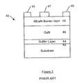
- FIG. 3An example of a prior art HEMT structure 40 is illustrated in FIG. 3.
- HEMT structure 40includes a substrate 42 , a buffer layer 44 , a GaN channel layer 46 and an AlGaN barrier layer 48 to which source, drain and gate contacts are made. Because the GaN channel layer 46 serves as the lattice template, the AlGaN barrier layer 48 is tensile strained.
- the thickness of the AlGaN barrier layer 48may be limited, which in turn limits the achievable carrier density in the channel of the transistor 40 .
- the transistor 10is designed such that, as the layers of the device are being epitaxially deposited, the total strain energy in the structure at no time exceeds a critical level that would cause cracking in the crystal structure.
- the strain in the GaN based channel layer 18is of opposite type to that of the strain in the AlGaN based barrier layer 20 such that the strains substantially offset each other and provide a substantially strain balanced device, thus keeping the strain below a critical threshold where damage occurs to the device.
- the resulting total strain energy of the devicemay be compressive or tensile.
Landscapes
- Junction Field-Effect Transistors (AREA)
Abstract
Description
- The present application is related to and claims priority from U.S. Provisional Application Serial No. 60/337,687, filed Dec. 3, 2001 and entitled “Strain Balanced Nitride Heterojunction Transistor” the disclosure of which is incorporated herein as if set forth fully herein.[0001]
- The present invention relates to high frequency transistors and in particular relates to a high electron mobility transistor (HEMT) that incorporates nitride-based active layers.[0002]
- The present invention relates to transistors formed of semiconductor materials that can make them suitable for high power, high temperature, and/or high frequency applications. Materials such as silicon (Si) and gallium arsenide (GaAs) have found wide application in semiconductor devices for lower power and (in the case of Si) lower frequency applications. These, more familiar, semiconductor materials may not be well suited for higher power and/or high frequency applications, however, because of their relatively small bandgaps (e.g., 1.12 eV for Si and 1.42 for GaAs at room temperature) and/or relatively small breakdown voltages.[0003]
- In light of the difficulties presented by Si and GaAs, interest in high power, high temperature and/or high frequency applications and devices has turned to wide bandgap semiconductor materials such as silicon carbide (2.996 eV for alpha SiC at room temperature) and the Group III nitrides (e.g., 3.36 eV for GaN at room temperature). These materials, typically, have higher electric field breakdown strengths and higher electron saturation velocities as compared to gallium arsenide and silicon.[0004]
- A device of particular interest for high power and/or high frequency applications is the high electron mobility transistor (HEMT), which is also known as a modulation doped field effect transistor (MODFET). These devices may offer operational advantages under a number of circumstances because a two-dimensional electron gas (2DEG) is formed at the heterojunction of two semiconductor materials with different bandgap energies, and where the smaller bandgap material has a higher electron affinity. The 2DEG is an accumulation layer in the undoped, smaller bandgap material and can contain a very high sheet electron concentration in excess of, for example, 10[0005]13carriers/cm2. Additionally, electrons that originate in the wider-bandgap semiconductor transfer to the 2DEG, allowing a high electron mobility due to reduced ionized impurity scattering.
- This combination of high carrier concentration and high carrier mobility can give the HEMT a very large transconductance and may provide a strong performance advantage over metal-semiconductor field effect transistors (MESFETs) for high-frequency applications.[0006]
- High electron mobility transistors fabricated in the gallium nitride/aluminum gallium nitride (GaN/AlGaN) material system have the potential to generate large amounts of RF power because of the combination of material characteristics that includes the aforementioned high breakdown fields, their wide bandgaps, large conduction band offset, and/or high saturated electron drift velocity. A major portion of the electrons in the 2DEG is attributed to polarization in the AlGaN.[0007]
- HEMTs in the GaN/AlGaN system have already been demonstrated. U.S. Pat. Nos. 5,192,987 and 5,296,395 describe AlGaN/GaN HEMT structures and methods of manufacture. U.S. Pat. No. 6,316,793, to Sheppard et al., which is commonly assigned and is incorporated herein by reference, describes a HEMT device having a semi-insulating silicon carbide substrate, an aluminum nitride buffer layer on the substrate, an insulating gallium nitride layer on the buffer layer, an aluminum gallium nitride barrier layer on the gallium nitride layer, and a passivation layer on the aluminum gallium nitride active structure.[0008]
- One limiting factor in the design of nitride-based HEMTs may be the aluminum concentration and thickness of the AlGaN barrier layer. In order to increase or maximize carrier concentration in the channel layer, it is desirable to have a relatively thick AlGaN barrier layer having a relatively high aluminum content. As described above, the AlGaN barrier layer is the source of carriers in the two dimensional electron gas. Accordingly a thicker barrier layer can supply more carriers to the channel. In addition, thicker AlGaN layers with higher aluminum compositions arc capable of producing larger piezoelectric fields and more spontaneous charge, that contribute to the formation of the two dimensional electron gas with high carrier concentration. However, thick AlGaN layers with high aluminum content tend to crack either during growth or after cooling, which destroys the device.[0009]
- Embodiments of the present invention provide a nitride based heterojunction transistor including a substrate and a first AlGaN based layer on the substrate. The first AlGaN based layer has an associated first strain energy. A GaN based layer is on the first AlGaN based layer. The GaN based layer has a bandgap that is less than a bandgap of the first AlGaN based layer and has an associated second strain energy. The second strain energy has a magnitude that is greater than a magnitude of the first strain energy. A second AlGaN based layer is on the GaN layer. The second AlGaN based layer has a bandgap that is greater than the bandgap of the GaN based layer and has an associated third strain energy. The third strain energy is of opposite strain type to the second strain energy. A source contact, a drain contact and a gate contact may also be provided on the second AlGaN based layer.[0010]
- In additional embodiments of the present invention, an AlN layer is provided on the GaN based layer and disposed between the GaN based layer and the second AlGaN based layer. In certain embodiments, the first AlGaN based layer is a short period super-lattice of AlN based layers and GaN based layers. In such embodiments, the AlN based layers and the GaN based layers of the short period super-lattice may be AlN layers and GaN layers respectively. The second AlGaN based layer may also be an Al[0011]xGa1-xN layer, where 0<x≦1.
- In further embodiments of the present invention, the first AlGaN based layer is a bottom confinement layer, the GaN layer is a channel layer and the second AlGaN based layer is a barrier layer. In further embodiments, the bottom confinement layer has a first aluminum concentration and the barrier layer has a second aluminum concentration different from the first aluminum concentration. The second aluminum concentration may be greater than the first aluminum concentration.[0012]
- In additional embodiments of the present invention, the second AlGaN based layer has a thickness and aluminum concentration large enough to induce formation of a 2D electron gas at the interface with the GaN based layer, but less than a thickness at which cracking or defect formation occurs. In particular embodiments of the present invention, the second AlGaN layer has a thickness of at least about 10 nm.[0013]
- In other embodiments of the present invention, the total strain energy in the first AlGaN based layer, the GaN based layer and the second AlGaN based layer at a growth temperature is approximately zero.[0014]
- In still further embodiments of the present invention, the first AlGaN based layer, the GaN layer and the second AlGaN based layer are substantially coherently strained in the “a” crystal lattice direction.[0015]
- In additional embodiments of the present invention, a buffer layer is provided between the substrate and the first AlGaN based layer. The buffer layer may be an AlN layer.[0016]
- In other embodiments of the present invention, the GaN based layer is directly on the first AlGaN based layer. The second AlGaN based layer may also be directly on the GaN based layer. The first AlGaN based layer may be a graded AlGaN based layer. The first AlGaN based layer may also be an AlGaN layer. Alternatively, the first AlGaN based layer may be an AlInGaN layer.[0017]
- In certain embodiments of the present invention, the first AlGaN based layer has an aluminum percentage of greater than about 10%. The second AlGaN based layer may also have an aluminum percentage of greater than about 20%. The first AlGaN based layer may have a thickness of at least about 1000 nm. The GaN based layer may have a thickness of from about 30 Å to about 300 Å. Alternatively, the GaN based layer may have a thickness of greater than about 500 Å. Furthermore, in certain embodiments, the substrate may be a silicon carbide substrate, a sapphire substrate, an AlN substrate and/or a silicon substrate.[0018]
- In further embodiments of the present invention, a method of fabricating a nitride based heterojunction transistor is provided by forming a substantially unstrained AlGaN based layer on a substrate, forming a compressive strained GaN based layer on the substantially unstrained AlGaN based layer and forming a tensile strained AlGaN based layer on the compressive strained GaN based layer. The tensile strained AlGaN based layer may be formed having a predefined tensile strain on the compressive strained GaN based layer. The predefined tensile strain may provide a tensile strain such that a total strain energy of the compressive strained GaN based layer and the tensile strained AlGaN based layer is about zero. The predefined tensile strain may be provided by adjusting the thickness of the tensile strained AlGaN based layer, a composition of the substantially unstrained AlGaN based layer and/or an aluminum concentration in the tensile strained AlGaN based layer to provide the predefined tensile strain.[0019]
- In additional embodiments of the present invention, the substantially unstrained AlGaN based layer is formed by forming three dimensional islands of AlGaN based material on the substrate and growing the AlGaN based material so that the AlGaN based material coalesces between the three dimensional islands to provide the substantially unstrained AlGaN based layer. The substantially unstrained AlGaN based layer may be a substantially unstrained AlGaN layer. Alternatively, the substantially unstrained AlGaN based layer may be a substantially unstrained AlInGaN layer. The tensile strained AlGaN based layer may be a tensile strained AlGaN layer. Alternatively, the tensile strained AlGaN based layer may be a tensile strained AlInGaN layer. Furthermore, the tensile strained AlGaN based layer may have a thickness of at least 10 nm. The compressive strained GaN based layer may have a thickness of from about 30 Å to about 300 Å. Alternatively, the compressive strained GaN based layer may have a thickness of greater than about 500 Å.[0020]
- In still further embodiments of the present invention, the substantially unstrained AlGaN based layer is formed by forming a substantially unstrained AlGaN based layer having a first aluminum concentration and the tensile strained AlGaN based layer is formed by forming a tensile strained AlGaN based layer having a second aluminum concentration different from the first aluminum concentration. In particular embodiments, the second aluminum concentration is greater than the first aluminum concentration. Furthermore, the tensile strained AlGaN based layer may be provided by forming a tensile strained AlGaN based layer having a thickness and aluminum concentration large enough to induce formation of a 2D electron gas at the interface with the compressive strained GaN based layer, but less than a thickness at which cracking or defect formation occurs.[0021]
- In additional embodiments of the present invention, a nitride based heterojunction transistor includes an AlGaN based bottom confinement layer, a GaN based channel layer on the bottom confinement layer and an AlGaN based barrier layer on the channel layer. The barrier layer has a higher concentration of aluminum than the bottom confinement layer. The channel layer may have a thickness of from about 30 Å to about 300 Å. The barrier layer may have a thickness of at least about 10 nm. The bottom confinement layer may be provided, for example, on a silicon carbide substrate, a sapphire substrate, an AlN substrate and/or a silicon substrate. An AlN buffer layer between the silicon carbide substrate and the bottom confinement layer may also be provided. The bottom confinement layer may also be a graded AlGaN based layer. A GaN based contact layer may be provided on the barrier layer. The bottom confinement layer and the barrier layer may each have an aluminum concentration of greater than about 10%. Methods of fabricating such transistors are also provided.[0022]
- In still further embodiments of the present invention, a Group III-nitride based heterojunction transistor structure is provided having a substrate and a first Group III-nitride based layer on the substrate, the first Group III-nitride based layer having a first strain associated therewith. A second Group III-nitride based layer is on the first Group III-nitride based layer. The second Group III-nitride based layer has a bandgap that is less than a bandgap of the first Group III-nitride based layer and has a second strain associated therewith. The second strain has a magnitude that is greater than a magnitude of the first strain. A third Group III-nitride based layer is on the second Group III-nitride based layer opposite the first Group III-nitride based layer. The third Group III-nitride based layer has a bandgap that is greater than the bandgap of the second Group III-nitride based layer and has a third strain associated therewith, the third strain being of opposite strain type to the second strain. In additional embodiments of the present invention, the first Group III-nitride based layer is an Al[0023]xGa1-xlayer, where 0<x≦1. The second Group III-nitride based layer may be a GaN layer. The third Group III-nitride base layer may be an AlN layer. Methods of fabricating such transistors are also provided.
- FIG. 1 is a schematic drawing showing a transistor according to embodiments of the present invention.[0024]
- FIG. 2 is a diagram of the band energy of an embodiment of the present invention.[0025]
- FIG. 3 is a diagram of a prior art HEMT structure.[0026]
- FIG. 4 is a schematic drawing showing a transistor according to further embodiments of the present invention.[0027]
- The present invention now will be described more fully hereinafter with reference to the accompanying drawings, in which preferred embodiments of the invention are shown. This invention may, however, be embodied in many different forms and should not be construed as limited to the embodiments set forth herein; rather, these embodiments are provided so that this disclosure will be thorough and complete, and will fully convey the scope of the invention to those skilled in the art. Like numbers refer to like elements throughout. Furthermore, the various layers and regions illustrated in the figures are illustrated schematically. Accordingly, the present invention is not limited to the relative size and spacing illustrated in the accompanying figures. As will also be appreciated by those of skill in the art, references herein to a layer formed “on” a substrate or other layer may refer to the layer formed directly on the substrate or other layer or on an intervening layer or layers formed on the substrate or other layer.[0028]
- Embodiments of the present invention are schematically illustrated as a high electron mobility transistor (HEMT)[0029]10 in the cross-sectional view of FIG. 1. The
transistor 10 includes a semi-insulating silicon carbide (SiC)substrate 12 that may be, for example, 4H polytype of silicon carbide. Other silicon carbide candidate polytypes include the 3C, 6H, and 15R polytypes. The term “semi-insulating” is used descriptively rather than in an absolute sense. In particular embodiments of the present invention, the silicon carbide bulk crystal has a resistivity equal to or higher than about 1×10⁵Ω-cm at room temperature. - An optional aluminum[0030]
nitride buffer layer 14 is on thesubstrate 12 and provides an appropriate crystal structure transition between the silicon carbide substrate and the remainder of the device. Silicon carbide has a much closer crystal lattice match to Group III nitrides than does sapphire (Al2O3), which is a very common substrate material for Group III nitride devices. The closer lattice match may result in Group III nitride films of higher quality than those generally available on sapphire. Silicon carbide also has a very high thermal conductivity so that the total output power of Group III nitride devices on silicon carbide is, typically, not as limited by thermal dissipation of the substrate as in the case of the same devices formed on sapphire. Also, the availability of semi-insulating silicon carbide substrates may provide for device isolation and reduced parasitic capacitance. - Although silicon carbide is the preferred substrate material, embodiments of the present invention may utilize any suitable substrate, such as sapphire, aluminum nitride, aluminum gallium nitride, gallium nitride, silicon, GaAs, LGO, ZnO, LAO, InP and the like. In some embodiments, an appropriate buffer layer also may be formed.[0031]
- As used herein, the term “Group III nitride” refers to those semiconducting compounds formed between nitrogen and the elements in Group III of the periodic table, usually aluminum (Al), gallium (Ga), and/or indium (In). The term also refers to ternary and quaternary compounds such as AlGaN and AlInGaN. As is well understood by those in this art, the Group III elements can combine with nitrogen to form binary (e.g., GaN), ternary (e.g., AlGaN, AlInN), and quaternary (e.g., AlInGaN) compounds. These compounds all have empirical formulas in which one mole of nitrogen is combined with a total of one mole of the Group III elements. Accordingly, formulas such as Al[0032]xGa1-xN where 0≦x≦1 are often used to describe them.
- Appropriate SiC substrates are manufactured by, for example, Cree, Inc., of Durham, N. C., the assignee of the present invention, and the methods for producing are described, for example, U.S. Pat. Nos. Re. 34,861; 4,946,547; 5,200,022; and 6,218,680, the contents of which are incorporated herein by reference in their entirety. Similarly, techniques for epitaxial growth of Group III nitrides have been described in, for example, U.S. Pat. Nos. 5,210,051; 5,393,993; 5,523,589; and 5,292,501, the contents of which are also incorporated herein by reference in their entirety. Suitable structures for GaN-based HEMTs are described, for example, in commonly assigned U.S. Pat. No. 6,316,793 and U.S. application Ser. No. 09/904,333 filed Jul. 12,2001 for “ALUMINUM GALLIUM NITRIDE/GALLIUM NITRIDE HIGH ELECTRON MOBILITY TRANSISTORS HAVING A GATE CONTACT ON A GALLIUM NITRIDE BASED CAP SEGMENT AND METHODS OF FABRICATING SAME,” U.S. provisional application serial No. 60/290,195 filed May 11, 2001 for “GROUP III NITRIDE BASED HIGH ELECTRON MOBILITY TRANSISTOR (HEMT) WITH BARRIER/SPACER LAYER” and U.S. patent application Ser. No. 10/102,272, to Smorchkova et al., entitled “GROUP-III NITRIDE BASED HIGH ELECTRON MOBILITY TRANSISTOR (HEMT) WITH BARRIER/SPACER LAYER” the disclosures of which are hereby incorporated herein by reference in their entirety.[0033]
- Returning to FIG. 1, the[0034]
transistor 10 includes abottom confinement layer 16 and achannel layer 18. Thebottom confinement layer 16 has a bandgap larger than that ofchannel layer 18. In certain embodiments of the present invention, thebottom confinement layer 16 has a substantially lower strain energy than that of thechannel layer 18 and may be substantially relaxed (i.e. substantially unstrained). For example, the bottom confinement layer may have a strain that is about 0 or may have a strain that is from about 0 to about 100% the strain of thechannel layer 18. In certain embodiments of the present invention, thebottom confinement layer 16 has a stress of less than about 1 GPa. In some embodiments of the present invention, thebottom confinement layer 16 may comprise a Group III-nitride, such as AlGaN or AlInGaN and the AlGaN and AlInGaN may be substantially free of dopants, such as Si and Mg. Thebottom confinement layer 16 may be at least about 1000 nm thick, but is not so thick as to cause cracking or defect formation therein. Thebottom confinement layer 16 may be semi-insulating. In certain embodiments, thebottom confinement layer 16 is AlGaN with a substantially uniform aluminum concentration between about 1% and 100%, and preferably greater than 10%. Alternatively, thebottom confinement layer 16 may be graded with an increasing, decreasing and/or increasing and decreasing aluminum concentration to better match the lattice constant of thechannel layer 18. Thebottom confinement layer 16 may also be a short period super-lattice of alternating layers of AlN and GaN. The term AlGaN based layer may also refer to a super-lattice of AlN and GaN and/or AlGaN and AlN and/or GaN. - The[0035]
bottom confinement layer 16 may be fabricated as a substantially relaxed layer by forming three dimensional islands on thesubstrate 12 or thebuffer layer 14 and growing thebottom confinement layer 16 such that the AlGaN based material coalesces between the islands. Such growth can provide an AlGaN based layer that is substantially relaxed and does not take on the lattice constant of the underlying substrate. Formation of larger islands may be beneficial in reducing tensile strain. - For example, in certain embodiments of the present invention a semi-insulating AlN layer is deposited at high temperature (>1000° C.) on a semi-insulating SiC substrate as a nucleation/buffer layer. Next, a semi-insulating Al[0036]xGa1-xN layer (x˜0.1-0.2) is deposited at high temperature (>1000° C.) on the AlN layer. The growth conditions (such as temperature, pressure, V/III ratio, growth rate, thickness, etc.) are adjusted to ensure that the AlGaN is not coherently strained to the AlN layer. Preferably, the AlGaN will initially begin growth in a three-dimensional mode with a relatively low density of nuclei (<109cm−2). As would be appreciated by those of skill in the art in light of the present disclosure, the detailed growth conditions may differ depending on reactor geometry and, therefore, may be adjusted accordingly to achieve AlGaN with these properties.
- In further embodiments, the Al[0037]xGa1-xN layer is graded with composition x decreasing during the growth. Furthermore, the layers may be grown as described above, but without the AlN layer, such that the AlGaN is grown directly on the SiC substrate in a substantially relaxed manner as described above.
- In addition to the[0038]
optional buffer layer 14, thebottom confinement layer 16 may be formed on or above one or more optional intervening layers (not shown). If such is the case, the strain energy that such intervening layers impart to the overall structure should be taken into account as described below. - In some embodiments of the present invention, the[0039]
channel layer 18 is a Group III-nitride, such as AlxGa1-xN where 0≦x<1, provided that the bandgap of thechannel layer 18 is less than the bandgap of thebottom confinement layer 16. In certain embodiments of the present invention, x=0, indicating that thechannel layer 18 is GaN. Thechannel layer 18 may be undoped and may be grown to a thickness of between about 30 and about 300 Å. Thus, thechannel layer 18 may be thinner than those in conventional GaN HEMT devices, which are typically greater than 500 Å in thickness. Because of the confinement provided by thebottom confinement layer 16, there may be less “tailing” of carriers into the GaN layer. Thus, the resulting devices may exhibit more linearity than devices found in the prior art. Alternatively, if strain control is a consideration and additional confinement is less of a consideration, theGaN channel layer 18 may be grown thicker than 500 Å and the aluminum percentage in thebottom confinement layer 16 may be reduced. - Furthermore, the interface between the[0040]
bottom confinement layer 16 and thechannel layer 18 may be doped n-type. For example, the portion of thebottom confinement layer 16 adjacent the channel layer may be doped to about 3×1012cm−2. Such a doping at the interface may counteract the positive charge at the interface. Thechannel layer 18, or portions thereof adjacent thebottom confinement layer 16, may also be doped n-type. - A[0041]
barrier layer 20 is provided on thechannel layer 18. Like thebottom confinement layer 16, thebarrier layer 20 may be a Group III-nitride and has a bandgap larger than that of thechannel layer 18 and may be tensile strained as described below. Accordingly, thebarrier layer 20 may be AlGaN, AlInGaN and/or AlN. Thebarrier layer 20 may be at least about 10 nm thick, but is not so thick as to cause cracking or defect formation therein. Preferably, thebarrier layer 20 is undoped or doped with a concentration less than about 1019cm−3. In some embodiments of the present invention, thebarrier layer 20 is AlxGa1-xN where 0<x≦1. In certain embodiments of the present invention, thebarrier layer 20 comprises AlGaN with an aluminum concentration of between about 5% and about 100%. In specific embodiments of the present invention, the aluminum concentration is greater than about 10%. Furthermore, the aluminum concentration in thebarrier layer 20 may be greater than the aluminum concentration in thebottom confinement layer 16. - The barrier layer may also be provided with multiple layers as described in U.S. patent application Serial No. 10/102,272, to Smorchkova et al., entitled “GROUP-III NITRIDE BASED HIGH ELECTRON MOBILITY TRANSISTOR (HEMT) WITH BARRIER/SPACER LAYER” the disclosure of which is incorporated herein by reference as if set forth fully herein. Thus, embodiments of the present invention should not be construed as limiting the barrier layer to a single layer but may include, for example, barrier layers having combinations of GaN, AlGaN and/or AlN layers. For example, a GaN, AlN structure may be utilized to reduce or prevent contamination of the GaN layers by contact material that may result in alloy scattering. An example of a structure according to further embodiments of the present invention is illustrated in FIG. 4, where an AlN[0042]
nitride barrier layer 20′ is provided on the GaN basedlayer 18 and an AlxGa1-xN layer22, where 0≦x≦1, is provided on theAlN barrier layer 20′. Thus, theAlN barrier layer 20′ is provided on the GaN basedlayer 18 and disposed between the GaN basedlayer 18 and the AlGaN basedlayer 22. - An optional GaN contact layer or cap layer (not shown) may be provided on the[0043]
barrier layer 20 to facilitate the formation of contacts of thetransistor 10. An example of such a cap layer is disclosed in U.S. application Ser. No. 09/904,333 filed Jul. 12,2001 for “ALUMINUM GALLIUM NITRIDE/GALLIUM NITRIDE HIGH ELECTRON MOBILITY TRANSISTORS HAVING A GATE CONTACT ON A GALLIUM NITRIDE BASED CAP SEGMENT AND METHODS OF FABRICATING SAME,” which is referenced above. In addition, there may be a compositionally graded transition layer (not shown) between thebarrier layer 20 and the contact or cap layer. Thesource contact 35, thedrain contact 37 and thegate contact 36 may be fabricated as described in U.S. Pat. No. 6,316,793. - FIG. 2 illustrates the conduction band E[0044]cin the
transistor 10 versus height (x). Because of the presence of aluminum in the crystal lattice, AlGaN has a wider bandgap than GaN. Thus, the interface between thechannel layer 18 and thebarrier layer 20 forms a heterostructure in which the conduction and valence bands Ecand Evin thebarrier layer 20 are offset. Charge is induced due to the piezoelectric effect and spontaneous doping. The conduction band Ecdips below the Fermi level Efin the area of thechannel layer 18 that is immediately adjacent to thebarrier layer 20. Consequently, a two dimensional electron gas (2DEG)sheet charge region 15 is induced at the heterojunction between thechannel layer 16 and thebarrier layer 20, whilelayer 20 is depleted of mobile carriers due to the shape of the conduction band. However, because of the bandgap lineup and arrangement of piezoelectric charge, a similar sheet charge region is not induced at the interface between thechannel layer 18 and thebottom confinement layer 16. Instead, thebottom confinement layer 16 acts to confine mobile carriers in thechannel layer 18, thereby increasing the carrier concentration in thechannel layer 18. Furthermore, by doping a portion of thebottom confinement layer 16 and/or thechannel layer 18, charge at the interface between thebottom confinement layer 16 and thechannel layer 18 may be reduced, thereby reducing or eliminating a 2DHG (2D hole gas) region that may form at the interface between thebottom confinement layer 16 and thechannel layer 18. - Electrons in the 2DEG[0045]
sheet charge region 15 demonstrate high carrier mobility. The conductivity of this region is modulated by applying a voltage to thegate electrode 36. When a reverse voltage is applied, the conduction band in the vicinity ofconduction layer 15 is elevated above the Fermi level, and a portion of theconduction layer 15 is depleted of carriers, thereby preventing the flow of current from thesource 35 to thedrain 37. - As discussed above, one shortcoming with conventional HEMT strictures is cracking in the AlGaN barrier layer when the layer is grown above a certain critical thickness (which, typically, depends on device geometry, layer structure, growth conditions and other factors). It is desirable to have a thick, high Al-composition AlGaN barrier to increase or maximize carrier density in the[0046]
2DEG region 15. One cause of cracking in the barrier layer is accumulated strain energy in the structure. Accordingly, embodiments of the present invention may reduce the overall strain energy in the device by balancing the strain energy components contributed by various layers in the device. - In semiconductor crystal structures, typically, strain effects are present if two different materials are adjacent to one another. As a result, the preferred thickness for an epitaxial layer is a thickness that is appropriate for the other performance parameters of the device, but less than a critical thickness. The critical thickness is, typically, the maximum thickness that the layer can be grown in strained fashion before dislocations or cracks begin to propagate.[0047]
- The strain (“ε”) between two layers is often expressed as the difference in the crystal lattice parameters between the two layers (Δa) divided by the lattice parameter of one of the layers. The higher this strain value, the thinner the layer that can be grown between the two materials. Furthermore, in a multilayer structure such as illustrated in FIG. 1, the overall strain energy (“Σ”) is a function or summation of the individual layer strains, and is referred to as the “effective strain.” The overall strain energy or total strain energy may be a linear combination of the strain values or may be a weighted combination of strain energies. For example, the total strain energy may be a weighted sum of the squares of the strain values. Thus, the total strain energy may be proportional to[0048]

- where t[0049]iis the thickness of a layer i.
- Strain is generally described as being one of two modes, namely tensile or compressive. Compressive strain of a crystal lattice indicates that the crystal lattice is being compressed into a smaller than usual space, while tensile strain indicates that the crystal lattice is being stretched into a larger than usual space. A crystal lattice can withstand only a certain amount of strain, either compressive or tensile, before the lattice bonds begin to fail and cracks appear in the crystal.[0050]
- In some embodiments of the present invention, the[0051]
bottom confinement layer 16 acts as a relaxed or nearly relaxed template to define the strain contributed to the device by thechannel layer 18 andbarrier layer 20. Stated differently, thebottom confinement layer 16 is nearly relaxed; thus, the subsequent epitaxial layers of thetransistor 10 inherit the lattice constant ofbottom confinement layer 16, and are, therefore, “pseudomoiphically strained” to the extent their lattice constant differs from that of thebottom confinement layer 16. Thechannel layer 18 is compressively strained, while thebarrier layer 20 is tensile strained, which tends to balance the average or effective strain in the device. - Furthermore, the specific tensile strain and/or compressive strain of the[0052]
barrier layer 20 and thechannel layer 18 may be controlled by, for example, controlling the aluminum concentration in the respective layers. - As described above, the lattice constants of the[0053]
bottom confinement layer 16, thechannel layer 18 and thebarrier layer 20 are substantially the same in the “a” direction (i.e. horizontally across the page in FIG. 1). However, in the “c” direction (i.e. vertically or the thickness or growth direction) the lattice constants differ. Thus, strain is induced into thechannel layer 18 and thebarrier layer 20. In particular, the unstrained “a” lattice constant of thechannel layer 18 is larger than that of thebottom confinement layer 16 and thus, compressive strain is induced in thechannel layer 18 as thechannel layer 18 attempts to conform to the smaller lattice constantbottom confinement layer 16 on which it is grown. Similarly, the unstrained “a” lattice constant of thechannel layer 18 is also larger than that of thebarrier layer 20 and thus, tensile strain is induced in thebarrier layer 20 as thebarrier layer 20 attempts to conform to the larger latticeconstant channel layer 18 on which it is grown. While the embodiments illustrated in FIG. 1 are described with regard to particular directions of growth, the present invention should not be construed as limited to such embodiments but may be applied to layers that are coherently strained such that all have the same strained in-plane lattice constant. - In certain embodiments of the present invention, the total strain energy of the[0054]
transistor 10 is approximately equal to zero. As described above, the total strain energy may be weight average, a non-weighted average, a sum of squares or other such combination of strain energies. Furthermore, the total strain energy may be determined at room temperature. In some embodiments, a non-zero magnitude total strain energy may be provided at a growth temperature such that the total strain energy at room temperature is about zero. Thus, thebarrier layer 20 can be grown to a greater thickness than would otherwise be possible for a given amount of strain. As used herein, in some embodiments, the term “approximately zero” total strain energy means a total strain energy of less than a corresponding two layer structure with a lattice mismatch of about 0.1% while in other embodiments, “approximately zero” may mean an total strain energy of less than a corresponding two layer structure with a lattice mismatch of about 1%. - In particular embodiments of the present invention, the[0055]
bottom confinement layer 16 may be AlxGa1-xN, thechannel layer 18 may be a GaN layer with a thickness of tGaNand thebarrier layer 20 may be AlyGa1-yN having a thickness of ty. In such embodiments, the values of x, y and the thicknesses tGaNand tymay satisfy the equation for linear weighting of strains:
- Thus, for example, in such embodiments, if the[0057]
barrier layer 20 and thechannel layer 18 have the same thickness then x may be about ½y. - For example, two SiC wafers were used to grow two different bottom layers, one of the present invention containing an Al[0058]xGa1-xN layer (x˜0.1-0.2) and the other using a conventional GaN layer. Upon both of these layers a GaN layer was deposited followed by a high aluminum AlxGa1-xN layer (x>0.4) with a thickness of 25 nm. For the layers grown on GaN layers, the AlGaN was cracked with a crack spacing on the order of only˜1 μm preventing any measurement of sheet resistivity. For the layers grown on AlGaN, the AlGaN layer was not cracked, and the sheet resistivity was only 300 Ω/□. This illustrates that the tensile stress in the top AlGaN layer can be effectively reduced to prevent cracking.
- In contrast to certain embodiments of the present invention, prior art HEMT structures incorporate a thick relaxed GaN layer as the bottom layer of the device, which then acts as the lattice template for the remaining layers of the device. In such devices, growing a thick, high aluminum percentage AlGaN barrier layer tends to impart too much strain energy to the structure, which can ultimately cause unwanted cracking to occur. An example of a prior[0059]
art HEMT structure 40 is illustrated in FIG. 3.HEMT structure 40 includes asubstrate 42, abuffer layer 44, aGaN channel layer 46 and anAlGaN barrier layer 48 to which source, drain and gate contacts are made. Because theGaN channel layer 46 serves as the lattice template, theAlGaN barrier layer 48 is tensile strained. As theAlGaN barrier layer 48 is made thicker or the aluminum percentage is increased, the strain energy imparted to the device by theAlGaN barrier layer 48 tends to increase, which can cause cracking as discussed above. Therefore, the thickness of theAlGaN barrier layer 48 may be limited, which in turn limits the achievable carrier density in the channel of thetransistor 40. - Returning to the discussion of the[0060]
transistor 10 of FIG. 1, through the use of strain control techniques according to some embodiments of the present invention, thetransistor 10 is designed such that, as the layers of the device are being epitaxially deposited, the total strain energy in the structure at no time exceeds a critical level that would cause cracking in the crystal structure. Thus, the strain in the GaN basedchannel layer 18 is of opposite type to that of the strain in the AlGaN basedbarrier layer 20 such that the strains substantially offset each other and provide a substantially strain balanced device, thus keeping the strain below a critical threshold where damage occurs to the device. The resulting total strain energy of the device may be compressive or tensile. - In the drawings and specification, there have been disclosed typical embodiments of the invention, and, although specific terms have been employed, they have been used in a generic and descriptive sense only and not for purposes of limitation, the scope of the invention being set forth in the following claims.[0061]


Claims (77)
1. A nitride based heterojunction transistor structure, comprising:
a substrate;
a first AlGaN based layer on the substrate, the first AlGaN based layer having a first strain associated therewith;
a GaN based layer on the first AlGaN based layer, the GaN based layer having a bandgap that is less than a bandgap of the first AlGaN based layer and having a second strain associated therewith, the second strain having a magnitude that is greater than a magnitude of the first strain; and
a second AlGaN based layer on the GaN layer opposite the first AlGaN based layer, the second AlGaN based layer having a bandgap that is greater than the bandgap of the GaN based layer and having a third strain associated therewith, the third strain being of opposite strain type to the second strain.
2. The nitride based heterojunction transistor structure according toclaim 1 , further comprising a source contact, a drain contact and a gate contact on the second AlGaN based layer.
3. The nitride based heterojunction transistor structure according toclaim 1 , further comprising an AlN layer on the GaN based layer and disposed between the GaN based layer and the second AlGaN based layer.
4. The nitride based heterojunction transistor structure according toclaim 1 , wherein the first AlGaN based layer comprises a short period super-lattice of AlN based layers and GaN based layers.
5. The nitride based heterojunction transistor structure ofclaim 4 , wherein the AlN based layers and the GaN based layers of the short period super-lattice comprise AlN layers and GaN layers respectively.
6. The nitride based heterojunction transistor structure ofclaim 1 , wherein the second AlGaN based layer comprises an AlxGa1-xN layer, where 0<x≦1.
7. The nitride based heterojunction transistor structure ofclaim 1 , wherein the first AlGaN based layer comprises a bottom confinement layer, the GaN layer comprises a channel layer and the second AlGaN based layer comprises a barrier layer.
8. The nitride based heterojunction transistor structure ofclaim 7 , wherein the bottom confinement layer has a first aluminum concentration and the barrier layer has a second aluminum concentration different from the first aluminum concentration.
9. The nitride based heterojunction transistor structure ofclaim 8 , wherein the second aluminum concentration is greater than the first aluminum concentration.
10. The nitride based heterojunction transistor structure ofclaim 1 , wherein the second AlGaN based layer has a thickness and aluminum concentration large enough to induce formation of a 2D electron gas at the interface with the GaN based layer, but less than a thickness at which cracking or defect formation occurs.
11. The nitride based heterojunction transistor structure ofclaim 1 , wherein the second AlGaN layer has a thickness of at least about 10 nm.
12. The nitride based heterojunction transistor structure ofclaim 1 , wherein a total strain energy in the first AlGaN based layer, the GaN based layer and the second AlGaN based layer is about zero.
13. The nitride based heterojunction transistor structure ofclaim 12 , wherein the total strain energy comprises a weighted sum of strains of layers of the heterojunction transistor.
14. The nitride based heterojunction transistor structure ofclaim 1 , wherein a total strain energy in the first AlGaN based layer, the GaN based layer and the second AlGaN based layer at room temperature is approximately zero.
15. The nitride based heterojunction transistor structure ofclaim 14 , wherein a magnitude of the total strain energy is greater than approximately zero at a growth temperature.
16. The nitride based heterojunction transistor structure ofclaim 1 , wherein the first AlGaN based layer, the GaN layer and the second AlGaN based layer are coherently strained such that all have the same strained in-plane lattice constant.
17. The nitride based heterojunction transistor structure ofclaim 1 , further comprising a buffer layer between the substrate and the first AlGaN based layer.
18. The nitride based heterojunction transistor structure ofclaim 17 , wherein the buffer layer comprises an AlN layer.
19. The nitride based heterojunction transistor structure ofclaim 1 , wherein the GaN based layer is directly on the first AlGaN based layer.
20. The nitride based heterojunction transistor structure ofclaim 19 , wherein the second AlGaN based layer is directly on the GaN based layer.
21. The nitride based heterojunction transistor structure ofclaim 1 , wherein the first AlGaN based layer is a graded AlGaN based layer.
22. The nitride based heterojunction transistor structure ofclaim 1 , wherein the first AlGaN based layer is an AlGaN layer.
23. The nitride based heterojunction transistor structure ofclaim 1 , wherein the first AlGaN based layer is an AlInGaN layer.
24. The nitride based heterojunction transistor structure ofclaim 1 , wherein the first AlGaN based layer has an aluminum percentage of greater than about 10%.
25. The nitride based heterojunction transistor structure ofclaim 1 , wherein the second AlGaN based layer has an aluminum percentage of greater than about 20%.
26. The nitride based heterojunction transistor structure ofclaim 1 , wherein the first AlGaN based layer has thickness of at least about 1000 nm.
27. The nitride based heterojunction transistor structure ofclaim 1 , wherein the GaN based layer has a thickness of from about 30 Å to about 300 Å.
28. The nitride based heterojunction transistor structure ofclaim 1 , wherein the GaN based layer has a thickness of greater than about 500 Å.
29. The nitride based heterojunction transistor structure ofclaim 1 , wherein the substrate comprises a silicon carbide substrate.
30. A method of fabricating a nitride based heterojunction transistor structure, comprising:
forming a substantially unstrained AlGaN based layer on a substrate;
forming a compressive strained GaN based layer on the substantially unstrained AlGaN based layer; and
forming a tensile strained AlGaN based layer on the compressive strained GaN based layer.
31. The method ofclaim 30 , wherein the step of forming a tensile strained AlGaN based layer comprises the step of forming a tensile strained AlGaN based layer having a predefined tensile strain on the compressive strained GaN based layer, the predefined tensile strain providing a tensile strain such that an total strain energy of the compressive strained GaN based layer and the tensile strained AlGaN based layer is about zero.
32. The method ofclaim 31 , wherein the predefined tensile strain is provided by adjusting at least one of a thickness of the tensile strained AlGaN based layer, a composition of the substantially unstrained AlGaN based layer and/or an aluminum concentration in the tensile strained AlGaN based layer to provide the predefined tensile strain.
33. The method ofclaim 31 , wherein the total strain energy comprises a linear summation of strain energies.
34. The method ofclaim 31 , wherein the total strain energy comprises a weighted summation of strain energies.
35. The method ofclaim 31 , wherein the total strain energy comprises a weighted sum of squares of the strain energy.
36. The method ofclaim 30 , wherein the step of forming a substantially unstrained AlGaN based layer comprises the steps of:
forming three dimensional islands of AlGaN based material on the substrate; and
growing the AlGaN based material so that the AlGaN based material coalesces between the three dimensional islands to provide the substantially unstrained AlGaN based layer.
37. The method ofclaim 30 , wherein the step of forming a substantially unstrained AlGaN based layer comprises forming a substantially unstrained AlGaN layer.
38. The method ofclaim 30 , wherein the step of forming a substantially unstrained AlGaN based layer comprises forming a substantially unstrained short period super-lattice of AlN and GaN based layers.
39. The method ofclaim 30 , wherein the step of forming a substantially unstrained AlGaN based layer comprises forming a substantially unstrained short period super-lattice of AlN and GaN layers.
40. The method ofclaim 30 , wherein the step of forming a substantially unstrained AlGaN based layer comprises forming a substantially unstrained AlInGaN layer.
41. The method ofclaim 30 , further comprising the step of forming a tensile strained AlN layer on the GaN based layer and disposed between the GaN based layer and the tensile strained AlGaN based layer.
42. The method ofclaim 30 , wherein the step of forming a tensile strained AlGaN based layer comprises forming a tensile strained AlGaN layer.
43. The method ofclaim 30 , wherein the step of forming a tensile strained AlGaN based layer comprises forming a tensile strained AlInGaN layer.
44. The method ofclaim 30 , wherein the step of forming a tensile strained AlGaN based layer comprises forming a tensile strained AlGaN based layer having a thickness of at least 10 nm.
45. The method ofclaim 30 , wherein the step of forming a compressive strained GaN based layer comprises forming a compressive strained GaN based layer having a thickness of from about 30 Å to about 300 Å.
46. The method ofclaim 30 , wherein the step of forming a compressive strained GaN based layer comprises forming a compressive strained GaN based layer having a thickness of greater than about 500 Å.
47. The method ofclaim 30 , wherein the step of forming a substantially unstrained AlGaN based layer comprises forming a substantially unstrained AlGaN based layer having a first aluminum concentration and the step of forming a tensile strained AlGaN based layer comprises forming a tensile strained AlGaN based layer having a second aluminum concentration different from the first aluminum concentration.
48. The method ofclaim 47 , wherein the second aluminum concentration is greater than the first aluminum concentration.
49. The method ofclaim 30 , wherein the step of forming a tensile strained AlGaN based layer comprises forming a tensile strained AlGaN based layer having a thickness and aluminum concentration large enough to induce formation of a 2D electron gas at the interface with the compressive strained GaN based layer, but less than a thickness at which cracking or defect formation occurs.
50. A nitride based heterojunction transistor, comprising:
an AlGaN based bottom confinement layer;
a GaN based channel layer on the bottom confinement layer; and
an AlGaN based barrier layer on the channel layer opposite the bottom confinement layer, the barrier layer having a higher concentration of aluminum than the bottom confinement layer.
51. The nitride based heterojunction transistor ofclaim 50 , wherein the channel layer has a thickness of from about 30 Å to about 300 Å.
52. The nitride based heterojunction transistor ofclaim 50 , wherein the barrier layer has a thickness of at least about 10 nm.
53. The nitride based heterojunction transistor ofclaim 50 , wherein the bottom confinement layer is on a silicon carbide substrate.
54. The nitride based heterojunction transistor ofclaim 53 , further comprising an AlN buffer layer between the silicon carbide substrate and the bottom confinement layer.
55. The nitride based heterojunction transistor ofclaim 50 , wherein the bottom confinement layer is a graded AlGaN based layer.
56. The nitride based heterojunction transistor ofclaim 50 further comprising a GaN based contact layer on the barrier layer.
57. The nitride based heterojunction transistor ofclaim 50 , wherein the bottom confinement layer has an aluminum concentration of greater than about 10%.
58. The nitride based heterojunction transistor ofclaim 50 , wherein the barrier layer has an aluminum concentration of greater than about 20%.
59. The nitride based heterojuntion transistor ofclaim 50 , further comprising an AlN based layer on the GaN based layer and disposed between the GaN based channel layer and the AlGaN based barrier layer.
60. A method of fabricating a nitride based heterojunction transistor, comprising:
forming an AlGaN based bottom confinement layer on a substrate;
forming a GaN based channel layer on the bottom confinement layer; and
forming an AlGaN based barrier layer on the channel layer, the barrier layer having a higher concentration of aluminum than the bottom confinement layer.
61. The method ofclaim 60 , wherein the channel layer is formed to a thickness of from about 30 Å to about 300 Å.
62. The method ofclaim 60 , wherein the barrier layer is formed to a thickness of at least about 10 nm.
63. The method ofclaim 60 , wherein the step of forming an AlGaN based bottom confinement layer comprises forming an AlGaN based bottom confinement layer on a silicon carbide substrate.
64. The method ofclaim 63 , further comprising forming an AlN buffer layer on the silicon carbide substrate and wherein the step of forming an AlGaN based bottom confinement layer comprises forming an AlGaN based bottom confinement layer on the buffer layer.
65. The method ofclaim 60 , wherein the step of forming an AlGaN based bottom confinement layer comprises forming a graded AlGaN based layer.
66. The method ofclaim 60 further comprising forming a GaN based contact layer on the barrier layer.
67. The method ofclaim 60 , wherein the bottom confinement layer has an aluminum concentration of greater than about 10%.
68. The method ofclaim 60 , wherein the barrier layer has an aluminum concentration of greater than about 20%.
69. The method ofclaim 60 , further comprising the step of forming an AlN layer on the GaN based layer and disposed between the GaN based channel layer and the AlGaN based barrier layer.
70. A Group III-nitride based heterojunction transistor structure, comprising:
a substrate;
a first Group III-nitride based layer on the substrate, the first Group III-nitride based layer having a first strain associated therewith;
a second Group III-nitride based layer on the first Group III-nitride based layer, the second Group III-nitride based layer having a bandgap that is less than a bandgap of the first Group III-nitride based layer and having a second strain associated therewith, the second strain having a magnitude that is greater than a magnitude of the first strain; and
a third Group III-nitride based layer on the second Group III-nitride based layer opposite the first Group III-nitride based layer, the third Group III-nitride based layer having a bandgap that is greater than the bandgap of the second Group III-nitride based layer and having a third strain associated therewith, the third strain being of opposite strain type to the second strain.
71. The Group III nitride based heterojunction transistor structure according toclaim 70 , wherein the first Group III-nitride based layer comprises an AlxGa1-xN layer, where 0<x<1.
72. The Group III nitride based heterojunction transistor structure according toclaim 71 , wherein the second Group III-nitride based layer comprise a GaN layer.
73. The Group III nitride based heterojunction transistor structure according toclaim 72 , wherein the third Group III-nitride base layer comprises an AlN layer.
74. A method of fabricating a Group III-nitride based heterojunction transistor structure, comprising:
forming a first Group III-nitride based layer on a substrate, the first Group III-nitride based layer having a first strain associated therewith;
forming a second Group III-nitride based layer on the first Group III-nitride based layer, the second Group III-nitride based layer having a bandgap that is less than a bandgap of the first Group III-nitride based layer and having a second strain associated therewith, the second strain having a magnitude that is greater than a magnitude of the first strain; and
forming a third Group III-nitride based layer on the second Group III-nitride based layer opposite the first Group III-nitride based layer, the third Group III-nitride based layer having a bandgap that is greater than the bandgap of the second Group III-nitride based layer and having a third strain associated therewith, the third strain being of opposite strain type to the second strain.
75. The method ofclaim 74 , wherein the step of forming a first Group III-nitride based layer comprises forming an AlxGa1-xN layer, where 0<x<1.
76. The method ofclaim 75 , wherein the step of forming a second Group III-nitride based layer comprises forming a GaN layer.
77. The method ofclaim 76 , wherein the step of forming a third Group III-nitride based layer comprises forming an AlN layer.
Priority Applications (12)
| Application Number | Priority Date | Filing Date | Title |
|---|---|---|---|
| US10/199,786US7030428B2 (en) | 2001-12-03 | 2002-07-19 | Strain balanced nitride heterojunction transistors |
| CN028241843ACN1599960B (en) | 2001-12-03 | 2002-11-20 | Strain balanced nitride heterojunction transistors and methods of fabricating strain balanced nitride heterojunction transistors |
| KR1020047008346AKR20050058259A (en) | 2001-12-03 | 2002-11-20 | Strain balanced nitride heterojunction transistors and methods of fabricating strain balanced nitride heterojunction transistors |
| AU2002352817AAU2002352817A1 (en) | 2001-12-03 | 2002-11-20 | Strain balanced nitride heterojunction transistors and methods of fabricating strain balanced nitride heterojunction transistors |
| CA002468520ACA2468520A1 (en) | 2001-12-03 | 2002-11-20 | Strain balanced nitride heterojunction transistors and methods of fabricating strain balanced nitride heterojunction transistors |
| AT02789772TATE525752T1 (en) | 2001-12-03 | 2002-11-20 | VOLTAGE BALANCED NITRIDE HETEROJUNCTION TRANSISTOR AND METHODS FOR PRODUCING THE SAME |
| JP2003550289AJP2005512327A (en) | 2001-12-03 | 2002-11-20 | Heterojunction transistor and manufacturing method thereof |
| PCT/US2002/037244WO2003049193A1 (en) | 2001-12-03 | 2002-11-20 | Strain balanced nitride heterojunction transistors and methods of fabricating strain balanced nitride heterojunction transistors |
| EP02789772AEP1456889B1 (en) | 2001-12-03 | 2002-11-20 | Strain balanced nitride heterojunction transistors and methods of fabricating the same |
| TW091134776ATWI255551B (en) | 2001-12-03 | 2002-11-29 | Strain balanced nitride heterojunction transistors and methods of fabricating strain balanced nitride heterojunction transistors |
| US11/325,735US8153515B2 (en) | 2001-12-03 | 2006-01-05 | Methods of fabricating strain balanced nitride heterojunction transistors |
| JP2011270859AJP6059428B2 (en) | 2001-12-03 | 2011-12-12 | Heterojunction transistor and manufacturing method thereof |
Applications Claiming Priority (2)
| Application Number | Priority Date | Filing Date | Title |
|---|---|---|---|
| US33768701P | 2001-12-03 | 2001-12-03 | |
| US10/199,786US7030428B2 (en) | 2001-12-03 | 2002-07-19 | Strain balanced nitride heterojunction transistors |
Related Child Applications (1)
| Application Number | Title | Priority Date | Filing Date |
|---|---|---|---|
| US11/325,735DivisionUS8153515B2 (en) | 2001-12-03 | 2006-01-05 | Methods of fabricating strain balanced nitride heterojunction transistors |
Publications (2)
| Publication Number | Publication Date |
|---|---|
| US20030102482A1true US20030102482A1 (en) | 2003-06-05 |
| US7030428B2 US7030428B2 (en) | 2006-04-18 |
Family
ID=26895154
Family Applications (2)
| Application Number | Title | Priority Date | Filing Date |
|---|---|---|---|
| US10/199,786Expired - LifetimeUS7030428B2 (en) | 2001-12-03 | 2002-07-19 | Strain balanced nitride heterojunction transistors |
| US11/325,735Expired - LifetimeUS8153515B2 (en) | 2001-12-03 | 2006-01-05 | Methods of fabricating strain balanced nitride heterojunction transistors |
Family Applications After (1)
| Application Number | Title | Priority Date | Filing Date |
|---|---|---|---|
| US11/325,735Expired - LifetimeUS8153515B2 (en) | 2001-12-03 | 2006-01-05 | Methods of fabricating strain balanced nitride heterojunction transistors |
Country Status (10)
| Country | Link |
|---|---|
| US (2) | US7030428B2 (en) |
| EP (1) | EP1456889B1 (en) |
| JP (2) | JP2005512327A (en) |
| KR (1) | KR20050058259A (en) |
| CN (1) | CN1599960B (en) |
| AT (1) | ATE525752T1 (en) |
| AU (1) | AU2002352817A1 (en) |
| CA (1) | CA2468520A1 (en) |
| TW (1) | TWI255551B (en) |
| WO (1) | WO2003049193A1 (en) |
Cited By (118)
| Publication number | Priority date | Publication date | Assignee | Title |
|---|---|---|---|---|
| US20030198869A1 (en)* | 2002-04-22 | 2003-10-23 | West Robert C. | Cross-linked polysiloxanes |
| US20040012015A1 (en)* | 2002-07-19 | 2004-01-22 | Saxler Adam William | Strain compensated semiconductor structures and methods of fabricating strain compensated semiconductor structures |
| US20040061129A1 (en)* | 2002-07-16 | 2004-04-01 | Saxler Adam William | Nitride-based transistors and methods of fabrication thereof using non-etched contact recesses |
| US20040115853A1 (en)* | 2002-12-11 | 2004-06-17 | Junko Kobayashi | Growth of III-nitride films on mismatched substrates without conventional low temperature nucleation layers |
| US6777278B2 (en) | 2000-12-01 | 2004-08-17 | Cree, Inc. | Methods of fabricating aluminum gallium nitride/gallium nitride high electron mobility transistors having a gate contact on a gallium nitride based cap segment |
| US20040209402A1 (en)* | 2003-03-18 | 2004-10-21 | Crystal Photonics, Incorporated | Method for making Group III nitride devices and devices produced thereby |
| US20050133816A1 (en)* | 2003-12-19 | 2005-06-23 | Zhaoyang Fan | III-nitride quantum-well field effect transistors |
| US20050164482A1 (en)* | 2004-01-22 | 2005-07-28 | Cree, Inc. | Silicon Carbide on Diamond Substrates and Related Devices and Methods |
| US20050170574A1 (en)* | 2004-01-16 | 2005-08-04 | Sheppard Scott T. | Nitride-based transistors with a protective layer and a low-damage recess and methods of fabrication thereof |
| US20050258431A1 (en)* | 2004-05-22 | 2005-11-24 | Smith Richard P | Dielectric passivation for semiconductor devices |
| US20050258451A1 (en)* | 2004-05-20 | 2005-11-24 | Saxler Adam W | Methods of fabricating nitride-based transistors having regrown ohmic contact regions and nitride-based transistors having regrown ohmic contact regions |
| US20050258450A1 (en)* | 2004-05-20 | 2005-11-24 | Saxler Adam W | Semiconductor devices having a hybrid channel layer, current aperture transistors and methods of fabricating same |
| US20060017064A1 (en)* | 2004-07-26 | 2006-01-26 | Saxler Adam W | Nitride-based transistors having laterally grown active region and methods of fabricating same |
| US20060019435A1 (en)* | 2004-07-23 | 2006-01-26 | Scott Sheppard | Methods of fabricating nitride-based transistors with a cap layer and a recessed gate |
| US20060054929A1 (en)* | 2002-05-31 | 2006-03-16 | Tatsuo Nakayama | Semiconductor device |
| US20060075958A1 (en)* | 2004-09-21 | 2006-04-13 | Adrian Powell | Low basal plane dislocation bulk grown SiC wafers |
| US7030428B2 (en) | 2001-12-03 | 2006-04-18 | Cree, Inc. | Strain balanced nitride heterojunction transistors |
| US20060102926A1 (en)* | 2004-11-16 | 2006-05-18 | Fujitsu Limited | Compound semiconductor device and the fabricating method of the same |
| US20060108606A1 (en)* | 2004-11-23 | 2006-05-25 | Saxler Adam W | Cap layers and/or passivation layers for nitride-based transistors, transistor structures and methods of fabricating same |
| US20060118823A1 (en)* | 2004-12-06 | 2006-06-08 | Primit Parikh | Field effect transistors (FETs) having multi-watt output power at millimeter-wave frequencies |
| US20060118809A1 (en)* | 2004-12-06 | 2006-06-08 | Primit Parikh | High power density and/or linearity transistors |
| US20060160345A1 (en)* | 2005-01-14 | 2006-07-20 | Xing-Quan Liu | Innovative growth method to achieve high quality III-nitride layers for wide band gap optoelectronic and electronic devices |
| US20060208280A1 (en)* | 2005-03-15 | 2006-09-21 | Smith Richard P | Group III nitride field effect transistors (FETS) capable of withstanding high temperature reverse bias test conditions |
| US20060225645A1 (en)* | 2005-04-07 | 2006-10-12 | Adrian Powell | Three inch silicon carbide wafer with low warp, bow, and TTV |
| US20060226412A1 (en)* | 2005-04-11 | 2006-10-12 | Saxler Adam W | Thick semi-insulating or insulating epitaxial gallium nitride layers and devices incorporating same |
| US20060226413A1 (en)* | 2005-04-11 | 2006-10-12 | Saxler Adam W | Composite substrates of conductive and insulating or semi-insulating group III-nitrides for group III-nitride devices |
| US20060244010A1 (en)* | 2005-04-29 | 2006-11-02 | Saxler Adam W | Aluminum free group III-nitride based high electron mobility transistors and methods of fabricating same |
| US20060255364A1 (en)* | 2004-02-05 | 2006-11-16 | Saxler Adam W | Heterojunction transistors including energy barriers and related methods |
| US20070004184A1 (en)* | 2005-06-29 | 2007-01-04 | Saxler Adam W | Low dislocation density group III nitride layers on silicon carbide substrates and methods of making the same |
| US20070018199A1 (en)* | 2005-07-20 | 2007-01-25 | Cree, Inc. | Nitride-based transistors and fabrication methods with an etch stop layer |
| US20070018198A1 (en)* | 2005-07-20 | 2007-01-25 | Brandes George R | High electron mobility electronic device structures comprising native substrates and methods for making the same |
| US7170111B2 (en) | 2004-02-05 | 2007-01-30 | Cree, Inc. | Nitride heterojunction transistors having charge-transfer induced energy barriers and methods of fabricating the same |
| US20070059873A1 (en)* | 2003-09-09 | 2007-03-15 | Alessandro Chini | Fabrication of single or multiple gate field plates |
| US20070164322A1 (en)* | 2006-01-17 | 2007-07-19 | Cree, Inc. | Methods of fabricating transistors including dielectrically-supported gate electrodes and related devices |
| US20070164315A1 (en)* | 2004-11-23 | 2007-07-19 | Cree, Inc. | Cap Layers Including Aluminum Nitride for Nitride-Based Transistors and Methods of Fabricating Same |
| US20070164314A1 (en)* | 2005-12-30 | 2007-07-19 | Robert Beach | Nitrogen polar III-nitride heterojunction JFET |
| US7253454B2 (en)* | 2005-03-03 | 2007-08-07 | Cree, Inc. | High electron mobility transistor |
| US20070194354A1 (en)* | 2006-02-23 | 2007-08-23 | Cree, Inc. | Nitride based transistors for millimeter wave operation |
| US20070210335A1 (en)* | 2004-04-30 | 2007-09-13 | The Furukawa Electric Co., Ltd. | GaN SEMICONDUCTOR DEVICE |
| CN100342547C (en)* | 2004-06-08 | 2007-10-10 | 中国科学院半导体研究所 | High-breakdown voltage transistor with high electronic mobility |
| CN100383980C (en)* | 2004-12-30 | 2008-04-23 | 中国科学院半导体研究所 | Structures to Improve Gate Schottky Performance of Gallium Nitride-Based High Electron Mobility Transistors |
| CN100397655C (en)* | 2004-12-02 | 2008-06-25 | 中国科学院半导体研究所 | Structure and manufacturing method for improving the performance of gallium nitride-based high electron mobility transistors |
| KR100848379B1 (en)* | 2004-06-11 | 2008-07-25 | 암모노 에스피. 제트오. 오. | High electron mobility transistor composed of VIIIII element nitride layer and its manufacturing method |
| US7419892B2 (en) | 2005-12-13 | 2008-09-02 | Cree, Inc. | Semiconductor devices including implanted regions and protective layers and methods of forming the same |
| EP1965433A2 (en) | 2006-11-21 | 2008-09-03 | Cree, Inc. | High voltage GaN transistors |
| CN100452322C (en)* | 2006-01-18 | 2009-01-14 | 中国科学院半导体研究所 | Silion carbide substrate gallium nitride high electronic transport ratio transistor and producing method |
| US20090014839A1 (en)* | 2006-02-09 | 2009-01-15 | Rohm Co., Ltd | Nitride-Based Semiconductor Device |
| US7525248B1 (en) | 2005-01-26 | 2009-04-28 | Ac Led Lighting, L.L.C. | Light emitting diode lamp |
| US7544963B2 (en) | 2005-04-29 | 2009-06-09 | Cree, Inc. | Binary group III-nitride based high electron mobility transistors |
| US20090146182A1 (en)* | 2007-12-10 | 2009-06-11 | Masahiro Hikita | Nitride semiconductor device and method for fabricating the same |
| US20090224289A1 (en)* | 2006-01-17 | 2009-09-10 | Cree, Inc. | Transistors including supported gate electrodes |
| US20100068855A1 (en)* | 2004-01-16 | 2010-03-18 | Cree, Inc. | Group III nitride semiconductor devices with silicon nitride layers and methods of manufacturing such devices |
| US20100276732A1 (en)* | 2007-12-26 | 2010-11-04 | Yuji Ando | Semiconductor device |
| US20110018040A1 (en)* | 2009-07-27 | 2011-01-27 | Smith R Peter | Methods of fabricating transistors including self-aligned gate electrodes and source/drain regions |
| US20110062448A1 (en)* | 2009-09-11 | 2011-03-17 | Samsung Electronics Co., Ltd. | Field effect semiconductor devices and methods of manufacturing field effect semiconductor devices |
| US7981744B2 (en) | 2004-06-10 | 2011-07-19 | Toyoda Gosei Co., Ltd. | Field-effect transistor, semiconductor device, a method for manufacturing them, and a method of semiconductor crystal growth |
| US20120025202A1 (en)* | 2010-07-30 | 2012-02-02 | Sumitomo Electric Industries, Ltd. | Semiconductor device and method for fabricating the same |
| WO2012054122A1 (en)* | 2010-10-20 | 2012-04-26 | National Semiconductor Corporation | Hemt with increased buffer breakdown voltage |
| US20120112202A1 (en)* | 2010-11-05 | 2012-05-10 | Samsung Electronics Co., Ltd. | E-Mode High Electron Mobility Transistors And Methods Of Manufacturing The Same |
| US8272757B1 (en) | 2005-06-03 | 2012-09-25 | Ac Led Lighting, L.L.C. | Light emitting diode lamp capable of high AC/DC voltage operation |
| US20130015463A1 (en)* | 2011-07-12 | 2013-01-17 | Samsung Electronics Co., Ltd. | Nitride-based semiconductor device having excellent stability |
| US8410472B2 (en) | 2008-12-15 | 2013-04-02 | Dowa Electronics Materials Co., Ltd. | Epitaxial substrate for electronic device and method of producing the same |
| US8426893B2 (en) | 2009-05-11 | 2013-04-23 | Dowa Electronics Materials Co., Ltd. | Epitaxial substrate for electronic device and method of producing the same |
| US8759879B1 (en)* | 2013-05-03 | 2014-06-24 | Texas Instruments Incorporated | RESURF III-nitride HEMTs |
| US8823057B2 (en) | 2006-11-06 | 2014-09-02 | Cree, Inc. | Semiconductor devices including implanted regions for providing low-resistance contact to buried layers and related devices |
| WO2014134310A1 (en)* | 2013-02-27 | 2014-09-04 | The University Of North Carolina At Charlotte | Incoherent type-iii materials for charge carriers control devices |
| US20140327011A1 (en)* | 2013-05-03 | 2014-11-06 | Texas Instruments Incorporated | Iii-nitride transistor layout |
| US20140367743A1 (en)* | 2005-12-28 | 2014-12-18 | Renesas Electronics Corporation | Field effect transistor, and multilayered epitaxial film for use in preparation of field effect transistor |
| US20150064859A1 (en)* | 2012-12-21 | 2015-03-05 | Lntel Corporation | Nonplanar iii-n transistors with compositionally graded semiconductor channels |
| CN104409496A (en)* | 2014-11-24 | 2015-03-11 | 电子科技大学 | Gallium-nitride-based power heterojunction field effect transistor with local back barrier |
| US20150249150A1 (en)* | 2012-12-17 | 2015-09-03 | Mitsubishi Electric Corporation | Transistor having nitride semiconductor used therein and method for manufacturing transistor having nitride semiconductor used therein |
| US9136344B2 (en) | 2012-03-26 | 2015-09-15 | Fujitsu Limited | Manufacturing method of semiconductor device, semiconductor device, and semiconductor crystal growth substrate |
| US20150357454A1 (en)* | 2013-02-15 | 2015-12-10 | Azurspace Solar Power Gmbh | Layer structure for a group-iii-nitride normally-off transistor |
| US20160225913A1 (en)* | 2013-08-30 | 2016-08-04 | Japan Science And Technology Agency | Ingaaln-based semiconductor device |
| CN105932041A (en)* | 2016-05-06 | 2016-09-07 | 西安电子科技大学 | N-face GaN-based fin high electron mobility transistor and manufacturing method |
| WO2016164765A1 (en)* | 2015-04-08 | 2016-10-13 | University Of Houston System | Externally-strain-engineered semiconductor photonic and electronic devices and assemblies and methods of making same |
| WO2017091817A1 (en)* | 2015-11-25 | 2017-06-01 | Texas Instruments Incorporated | Isolated iii-n semiconductor devices |
| US20170170295A1 (en)* | 2011-11-29 | 2017-06-15 | Taiwan Semiconductor Manufacturing Company, Ltd. | High electron mobility transistor structure |
| US9691857B2 (en) | 2011-12-19 | 2017-06-27 | Intel Corporation | Group III-N nanowire transistors |
| WO2017160707A1 (en) | 2016-03-17 | 2017-09-21 | Cree, Inc. | Transistor with bypassed gate structure |
| US9947616B2 (en) | 2016-03-17 | 2018-04-17 | Cree, Inc. | High power MMIC devices having bypassed gate transistors |
| EP3312870A1 (en)* | 2013-06-06 | 2018-04-25 | NGK Insulators, Ltd. | Group 13 nitride composite substrate, semiconductor element, and production method for group 13 nitride composite substrate |
| US10128365B2 (en) | 2016-03-17 | 2018-11-13 | Cree, Inc. | Bypassed gate transistors having improved stability |
| WO2018236682A1 (en) | 2017-06-21 | 2018-12-27 | Cree, Inc. | SEMICONDUCTOR DEVICES HAVING A PLURALITY OF UNITARY CELL TRANSISTORS WHICH HAVE A SMOKE START-UP BEHAVIOR AND IMPROVED LINEARITY |
| US10203526B2 (en) | 2015-07-06 | 2019-02-12 | The University Of North Carolina At Charlotte | Type III hetrojunction—broken gap HJ |
| WO2019070694A1 (en) | 2017-10-03 | 2019-04-11 | Cree, Inc. | Transistor amplifiers having node splitting for loop stability and related methods |
| US10312344B2 (en)* | 2016-09-28 | 2019-06-04 | Fujitsu Limited | Semiconductor device, manufacturing method of semiconductor device, power unit, and amplifier |
| US10483352B1 (en)* | 2018-07-11 | 2019-11-19 | Cree, Inc. | High power transistor with interior-fed gate fingers |
| CN111033750A (en)* | 2017-08-25 | 2020-04-17 | Hrl实验室有限责任公司 | Digital alloy-based back barrier for P-channel nitride transistors |
| WO2020106537A1 (en) | 2018-11-19 | 2020-05-28 | Cree, Inc. | Semiconductor devices having a plurality of unit cell transistors that have smoothed turn-on behavior and improved linearity |
| KR20200066141A (en)* | 2018-11-30 | 2020-06-09 | 한국산업기술대학교산학협력단 | Method for Manufacturing AlN Based Transistor |
| WO2020142345A2 (en) | 2019-01-03 | 2020-07-09 | Cree, Inc. | High electron mobility transistors having improved drain current drift and/or leakage current performance |
| WO2020111789A3 (en)* | 2018-11-30 | 2020-07-16 | 한국산업기술대학교산학협력단 | Method for manufacturing aluminum nitride-based transistor |
| EP2363890B1 (en)* | 2010-03-02 | 2020-08-19 | Samsung Electronics Co., Ltd. | High electron mobility transistors exhibiting dual depletion and methods of manufacturing the same |
| US10763334B2 (en) | 2018-07-11 | 2020-09-01 | Cree, Inc. | Drain and/or gate interconnect and finger structure |
| US10770415B2 (en) | 2018-12-04 | 2020-09-08 | Cree, Inc. | Packaged transistor devices with input-output isolation and methods of forming packaged transistor devices with input-output isolation |
| CN113436963A (en)* | 2021-06-28 | 2021-09-24 | 吉林大学 | Covering layer screening method for two-dimensional semiconductor modulation doping and obtained heterojunction |
| WO2021202674A2 (en) | 2020-04-03 | 2021-10-07 | Cree, Inc. | Rf amplifier devices and methods of manufacturing |
| WO2021202358A1 (en) | 2020-04-03 | 2021-10-07 | Cree, Inc. | Group iii nitride-based radio frequency transistor amplifiers having source, gate and/or drain conductive vias |
| WO2021202199A1 (en) | 2020-04-03 | 2021-10-07 | Cree, Inc. | Group iii nitride-based radio frequency amplifiers having back side source, gate and/or drain terminals |
| WO2021247317A1 (en) | 2020-06-01 | 2021-12-09 | Cree, Inc. | Rf amplifiers having shielded transmission line structures |
| WO2021262920A2 (en) | 2020-06-25 | 2021-12-30 | Cree, Inc. | Multi-zone radio frequency transistor amplifiers |
| WO2022055776A1 (en) | 2020-09-11 | 2022-03-17 | Cree, Inc. | Rf transistor amplifier package |
| CN114551593A (en)* | 2022-01-17 | 2022-05-27 | 江西兆驰半导体有限公司 | Epitaxial wafer, epitaxial wafer growth method and high-electron-mobility transistor |
| WO2022150264A1 (en) | 2021-01-08 | 2022-07-14 | Cree, Inc. | Radio frequency transistor amplifiers having widened and/or asymmetric source/drain regions for improved on-resistance performance |
| US11417746B2 (en) | 2019-04-24 | 2022-08-16 | Wolfspeed, Inc. | High power transistor with interior-fed fingers |
| CN115117150A (en)* | 2022-08-24 | 2022-09-27 | 成都功成半导体有限公司 | GaN HEMT power device and preparation method thereof |
| US11535951B1 (en)* | 2018-06-06 | 2022-12-27 | United States Of America As Represented By The Secretary Of The Air Force | Optimized thick heteroepitaxial growth of semiconductors with in-situ substrate pretreatment |
| WO2023056145A1 (en) | 2021-10-01 | 2023-04-06 | Wolfspeed, Inc. | Bypassed gate transistors having improved stability |
| US11670605B2 (en) | 2020-04-03 | 2023-06-06 | Wolfspeed, Inc. | RF amplifier devices including interconnect structures and methods of manufacturing |
| US11742304B2 (en) | 2018-07-19 | 2023-08-29 | Wolfspeed, Inc. | Radio frequency transistor amplifiers and other multi-cell transistors having isolation structures |
| US11742302B2 (en) | 2020-10-23 | 2023-08-29 | Wolfspeed, Inc. | Electronic device packages with internal moisture barriers |
| WO2023172403A1 (en) | 2022-03-08 | 2023-09-14 | Wolfspeed, Inc. | Group iii nitride-based monolithic microwave integrated circuits having multi-layer metal-insulator-metal capacitors |
| WO2024039968A2 (en) | 2022-08-18 | 2024-02-22 | Wolfspeed, Inc. | High electron mobility transistors having reduced drain current drift and methods of fabricating such devices |
| WO2024123239A1 (en)* | 2022-12-08 | 2024-06-13 | Nanyang Technological University | Heterostructure and method of forming the same |
| WO2024191770A2 (en) | 2023-03-15 | 2024-09-19 | Macom Technology Solutions Holdings, Inc. | Bypassed gate transistors having improved stability |
| CN118800795A (en)* | 2024-09-14 | 2024-10-18 | 北京中科重仪半导体科技有限公司 | An enhanced gallium nitride HEMT device with dual channels and a method for preparing the same |
| WO2024258898A1 (en) | 2023-06-14 | 2024-12-19 | Wolfspeed, Inc. | Rf amplifier package and manufacturing method thereof |
Families Citing this family (149)
| Publication number | Priority date | Publication date | Assignee | Title |
|---|---|---|---|---|
| JP4469139B2 (en)* | 2003-04-28 | 2010-05-26 | シャープ株式会社 | Compound semiconductor FET |
| JP3940699B2 (en)* | 2003-05-16 | 2007-07-04 | 株式会社東芝 | Power semiconductor device |
| US8107893B2 (en)* | 2003-07-15 | 2012-01-31 | Lockheed Martin Corporation | Method and apparatus for transmission and reception of signals |
| WO2005015642A1 (en)* | 2003-08-08 | 2005-02-17 | Sanken Electric Co., Ltd. | Semiconductor device and manufacturing method thereof |
| TWI295085B (en)* | 2003-12-05 | 2008-03-21 | Int Rectifier Corp | Field effect transistor with enhanced insulator structure |
| JP2005183551A (en)* | 2003-12-17 | 2005-07-07 | Nec Corp | Semiconductor device, field effect transistor, and method for manufacturing same |
| US8174048B2 (en)* | 2004-01-23 | 2012-05-08 | International Rectifier Corporation | III-nitride current control device and method of manufacture |
| JP4832722B2 (en)* | 2004-03-24 | 2011-12-07 | 日本碍子株式会社 | Semiconductor laminated structure and transistor element |
| US20050218414A1 (en)* | 2004-03-30 | 2005-10-06 | Tetsuzo Ueda | 4H-polytype gallium nitride-based semiconductor device on a 4H-polytype substrate |
| JP2005353817A (en)* | 2004-06-10 | 2005-12-22 | Toyoda Gosei Co Ltd | Field effect transistor and its manufacturing method |
| JP4682541B2 (en)* | 2004-06-15 | 2011-05-11 | 豊田合成株式会社 | Semiconductor crystal growth method |
| JP4729872B2 (en)* | 2004-06-15 | 2011-07-20 | 豊田合成株式会社 | Method for manufacturing field effect transistor |
| PL368483A1 (en)* | 2004-06-11 | 2005-12-12 | Ammono Sp.Z O.O. | Monocrystals of nitride containing gallium and its application |
| JP2006032911A (en) | 2004-06-15 | 2006-02-02 | Ngk Insulators Ltd | Semiconductor laminated structure, semiconductor element and HEMT element |
| US7525130B2 (en)* | 2004-09-29 | 2009-04-28 | The Regents Of The University Of California | Polarization-doped field effect transistors (POLFETS) and materials and methods for making the same |
| DE102004055636A1 (en)* | 2004-11-12 | 2006-05-24 | Azzurro Semiconductors Ag | Production of semiconductor elements for Bragg reflector involves growing epitaxial aluminum indium nitride layers, and changing aluminum-to-indium ratio during growth process |
| CN100379019C (en)* | 2004-12-09 | 2008-04-02 | 中国科学院半导体研究所 | Double heterostructure GaN-based high electron mobility transistor structure and fabrication method |
| US7236053B2 (en)* | 2004-12-31 | 2007-06-26 | Cree, Inc. | High efficiency switch-mode power amplifier |
| JP4832768B2 (en)* | 2005-02-09 | 2011-12-07 | 日本電信電話株式会社 | Semiconductor device |
| US8062780B2 (en) | 2005-03-17 | 2011-11-22 | Nec Corporation | Film-covered electric device and method of manufacturing same |
| JP4916671B2 (en)* | 2005-03-31 | 2012-04-18 | 住友電工デバイス・イノベーション株式会社 | Semiconductor device |
| KR100638818B1 (en)* | 2005-05-19 | 2006-10-27 | 삼성전기주식회사 | Nitride semiconductor light emitting device |
| JP4792814B2 (en)* | 2005-05-26 | 2011-10-12 | 住友電気工業株式会社 | High electron mobility transistor, field effect transistor, epitaxial substrate, method for producing epitaxial substrate, and method for producing group III nitride transistor |
| US7405430B2 (en)* | 2005-06-10 | 2008-07-29 | Cree, Inc. | Highly uniform group III nitride epitaxial layers on 100 millimeter diameter silicon carbide substrates |
| KR100706952B1 (en)* | 2005-07-22 | 2007-04-12 | 삼성전기주식회사 | Vertical structure gallium nitride-based light emitting diode device and method of manufacturing the same |
| EP1938385B1 (en)* | 2005-09-07 | 2014-12-03 | Cree, Inc. | Transistors with fluorine treatment |
| JP2007080896A (en)* | 2005-09-12 | 2007-03-29 | Sanyo Electric Co Ltd | Semiconductor element |
| JP2007088252A (en) | 2005-09-22 | 2007-04-05 | Toyoda Gosei Co Ltd | Field effect transistor |
| JP4705481B2 (en)* | 2006-01-25 | 2011-06-22 | パナソニック株式会社 | Nitride semiconductor device |
| US7560318B2 (en)* | 2006-03-13 | 2009-07-14 | Freescale Semiconductor, Inc. | Process for forming an electronic device including semiconductor layers having different stresses |
| JP4862442B2 (en)* | 2006-03-15 | 2012-01-25 | 日立電線株式会社 | Method for manufacturing group III-V nitride semiconductor substrate and method for manufacturing group III-V nitride device |
| US7388236B2 (en)* | 2006-03-29 | 2008-06-17 | Cree, Inc. | High efficiency and/or high power density wide bandgap transistors |
| JP5400266B2 (en)* | 2006-04-17 | 2014-01-29 | パナソニック株式会社 | Field effect transistor |
| US9040398B2 (en)* | 2006-05-16 | 2015-05-26 | Cree, Inc. | Method of fabricating seminconductor devices including self aligned refractory contacts |
| US7479465B2 (en)* | 2006-07-28 | 2009-01-20 | Freescale Semiconductor, Inc. | Transfer of stress to a layer |
| RU2316076C1 (en)* | 2006-11-14 | 2008-01-27 | Закрытое Акционерное Общество "Светлана-Рост" | Semiconductor heterostructure of field-effect transistor |
| CN101266999B (en)* | 2007-03-14 | 2010-05-19 | 中国科学院半导体研究所 | Gallium Nitride-Based Double Heterojunction Field Effect Transistor Structure and Fabrication Method |
| JP5292716B2 (en)* | 2007-03-30 | 2013-09-18 | 富士通株式会社 | Compound semiconductor device |
| TW200903805A (en)* | 2007-05-24 | 2009-01-16 | Univ California | Polarization-induced barriers for N-face nitride-based electronics |
| US8461626B2 (en)* | 2007-07-09 | 2013-06-11 | Freescale Semiconductor, Inc. | Hetero-structure field effect transistor, integrated circuit including a hetero-structure field effect transistor and method for manufacturing a hetero-structure field effect transistor |
| US7915643B2 (en) | 2007-09-17 | 2011-03-29 | Transphorm Inc. | Enhancement mode gallium nitride power devices |
| US20090072269A1 (en)* | 2007-09-17 | 2009-03-19 | Chang Soo Suh | Gallium nitride diodes and integrated components |
| US7800132B2 (en)* | 2007-10-25 | 2010-09-21 | Northrop Grumman Systems Corporation | High electron mobility transistor semiconductor device having field mitigating plate and fabrication method thereof |
| CN101971308B (en)* | 2008-03-12 | 2012-12-12 | 日本电气株式会社 | Semiconductor device |
| US8519438B2 (en) | 2008-04-23 | 2013-08-27 | Transphorm Inc. | Enhancement mode III-N HEMTs |
| US8289065B2 (en) | 2008-09-23 | 2012-10-16 | Transphorm Inc. | Inductive load power switching circuits |
| US7898004B2 (en) | 2008-12-10 | 2011-03-01 | Transphorm Inc. | Semiconductor heterostructure diodes |
| US20100276730A1 (en)* | 2009-04-29 | 2010-11-04 | University Of Seoul Industry Cooperation Foundation | Semiconductor device |
| US20100270591A1 (en)* | 2009-04-27 | 2010-10-28 | University Of Seoul Industry Cooperation Foundation | High-electron mobility transistor |
| US8253145B2 (en)* | 2009-04-29 | 2012-08-28 | University Of Seoul Industry Cooperation Foundation | Semiconductor device having strong excitonic binding |
| US20100270547A1 (en)* | 2009-04-27 | 2010-10-28 | University Of Seoul Industry Cooperation Foundation | Semiconductor device |
| US8097999B2 (en)* | 2009-04-27 | 2012-01-17 | University Of Seoul Industry Cooperation Foundation | Piezoelectric actuator |
| US20100270592A1 (en)* | 2009-04-27 | 2010-10-28 | University Of Seoul Industry Cooperation Foundation | Semiconductor device |
| US8742459B2 (en) | 2009-05-14 | 2014-06-03 | Transphorm Inc. | High voltage III-nitride semiconductor devices |
| US8269253B2 (en)* | 2009-06-08 | 2012-09-18 | International Rectifier Corporation | Rare earth enhanced high electron mobility transistor and method for fabricating same |
| US20100327278A1 (en)* | 2009-06-29 | 2010-12-30 | University Of Seoul Industry Cooperation Foundation | Laminated structures |
| JP2011049488A (en)* | 2009-08-28 | 2011-03-10 | Sumitomo Electric Ind Ltd | Group iii nitride semiconductor laminate wafer and group iii nitride semiconductor device |
| US8390000B2 (en) | 2009-08-28 | 2013-03-05 | Transphorm Inc. | Semiconductor devices with field plates |
| KR20110032845A (en)* | 2009-09-24 | 2011-03-30 | 삼성전자주식회사 | Power electronic device and manufacturing method |
| JP5193150B2 (en)* | 2009-09-24 | 2013-05-08 | 日本電信電話株式会社 | Nitride semiconductor device and manufacturing method thereof |
| JP2011071356A (en)* | 2009-09-26 | 2011-04-07 | Sanken Electric Co Ltd | Semiconductor device |
| TWI462286B (en)* | 2009-12-10 | 2014-11-21 | 同和電子科技股份有限公司 | A epitaxial substrate for electronic components and a method for manufacturing the same |
| US8389977B2 (en) | 2009-12-10 | 2013-03-05 | Transphorm Inc. | Reverse side engineered III-nitride devices |
| JP5758880B2 (en)* | 2010-03-24 | 2015-08-05 | 日本碍子株式会社 | Epitaxial substrate for semiconductor element, semiconductor element, and method for producing epitaxial substrate for semiconductor element |
| US8921894B2 (en)* | 2010-03-26 | 2014-12-30 | Nec Corporation | Field effect transistor, method for producing the same, and electronic device |
| US20130099245A1 (en)* | 2010-03-26 | 2013-04-25 | Nec Corporation | Field effect transistor, method for producing the same, and electronic device |
| CN102315126A (en)* | 2010-07-07 | 2012-01-11 | 中国科学院微电子研究所 | Semiconductor device and manufacturing method thereof |
| CN101916773B (en)* | 2010-07-23 | 2012-05-23 | 中国科学院上海技术物理研究所 | Double-channel MOS-HEMT (Metal Oxide Semiconductor-High Electron Mobility Transistor) device and manufacturing method |
| JP5781292B2 (en)* | 2010-11-16 | 2015-09-16 | ローム株式会社 | Nitride semiconductor device and nitride semiconductor package |
| JP5810293B2 (en)* | 2010-11-19 | 2015-11-11 | パナソニックIpマネジメント株式会社 | Nitride semiconductor device |
| US8742460B2 (en) | 2010-12-15 | 2014-06-03 | Transphorm Inc. | Transistors with isolation regions |
| US8643062B2 (en) | 2011-02-02 | 2014-02-04 | Transphorm Inc. | III-N device structures and methods |
| US8716141B2 (en) | 2011-03-04 | 2014-05-06 | Transphorm Inc. | Electrode configurations for semiconductor devices |
| US8772842B2 (en) | 2011-03-04 | 2014-07-08 | Transphorm, Inc. | Semiconductor diodes with low reverse bias currents |
| JP2012190852A (en)* | 2011-03-08 | 2012-10-04 | Sumitomo Electric Ind Ltd | Group iii nitride semiconductor electronic device, epitaxial substrate, and method for manufacturing group iii nitride semiconductor electronic device |
| KR101616156B1 (en)* | 2011-07-19 | 2016-04-27 | 한국전자통신연구원 | Nitride electronic device and method for manufacturing it |
| US8723222B2 (en)* | 2011-07-19 | 2014-05-13 | Electronics And Telecommunications Research Institute | Nitride electronic device and method for manufacturing the same |
| US8710511B2 (en) | 2011-07-29 | 2014-04-29 | Northrop Grumman Systems Corporation | AIN buffer N-polar GaN HEMT profile |
| US8901604B2 (en) | 2011-09-06 | 2014-12-02 | Transphorm Inc. | Semiconductor devices with guard rings |
| US9257547B2 (en) | 2011-09-13 | 2016-02-09 | Transphorm Inc. | III-N device structures having a non-insulating substrate |
| US20130082274A1 (en)* | 2011-09-29 | 2013-04-04 | Bridgelux, Inc. | Light emitting devices having dislocation density maintaining buffer layers |
| US8598937B2 (en) | 2011-10-07 | 2013-12-03 | Transphorm Inc. | High power semiconductor electronic components with increased reliability |
| JP2013140866A (en) | 2012-01-04 | 2013-07-18 | Renesas Electronics Corp | Semiconductor device, and method of manufacturing the same |
| JP5785103B2 (en)* | 2012-01-16 | 2015-09-24 | シャープ株式会社 | Epitaxial wafers for heterojunction field effect transistors. |
| US9165766B2 (en) | 2012-02-03 | 2015-10-20 | Transphorm Inc. | Buffer layer structures suited for III-nitride devices with foreign substrates |
| JP2013171854A (en)* | 2012-02-17 | 2013-09-02 | Mitsubishi Electric Corp | Semiconductor device and manufacturing method of the same |
| US8916909B2 (en)* | 2012-03-06 | 2014-12-23 | Infineon Technologies Austria Ag | Semiconductor device and method for fabricating a semiconductor device |
| WO2013155108A1 (en) | 2012-04-09 | 2013-10-17 | Transphorm Inc. | N-polar iii-nitride transistors |
| JP5796181B2 (en)* | 2012-05-22 | 2015-10-21 | パナソニックIpマネジメント株式会社 | Nitride semiconductor light emitting device |
| US9184275B2 (en) | 2012-06-27 | 2015-11-10 | Transphorm Inc. | Semiconductor devices with integrated hole collectors |
| TWI495154B (en)* | 2012-12-06 | 2015-08-01 | Genesis Photonics Inc | Semiconductor structure |
| EP2747143A1 (en)* | 2012-12-19 | 2014-06-25 | Nxp B.V. | GaN HEMTs and GaN diodes |
| CN105164811B (en) | 2013-02-15 | 2018-08-31 | 创世舫电子有限公司 | Electrode of semiconductor devices and forming method thereof |
| US9087718B2 (en) | 2013-03-13 | 2015-07-21 | Transphorm Inc. | Enhancement-mode III-nitride devices |
| US8866154B2 (en) | 2013-03-14 | 2014-10-21 | Wisconsin Alumni Research Foundation | Lattice mismatched heterojunction structures and devices made therefrom |
| US9245992B2 (en) | 2013-03-15 | 2016-01-26 | Transphorm Inc. | Carbon doping semiconductor devices |
| RU2534437C1 (en)* | 2013-07-04 | 2014-11-27 | Открытое акционерное общество "Научно-производственное предприятие "Пульсар" | Heterostructure modulated-doped field-effect transistor |
| US9412911B2 (en) | 2013-07-09 | 2016-08-09 | The Silanna Group Pty Ltd | Optical tuning of light emitting semiconductor junctions |
| US9443938B2 (en) | 2013-07-19 | 2016-09-13 | Transphorm Inc. | III-nitride transistor including a p-type depleting layer |
| JP5698321B2 (en)* | 2013-08-09 | 2015-04-08 | Dowaエレクトロニクス株式会社 | Group III nitride semiconductor epitaxial substrate, group III nitride semiconductor light emitting device, and method for manufacturing the same |
| JP6305041B2 (en)* | 2013-12-06 | 2018-04-04 | 住友化学株式会社 | Nitride semiconductor laminate and nitride semiconductor device |
| JP2015115429A (en)* | 2013-12-11 | 2015-06-22 | シャープ株式会社 | Nitride semiconductor epitaxial substrate and nitride semiconductor device |
| JP2015176936A (en)* | 2014-03-13 | 2015-10-05 | 株式会社東芝 | semiconductor device |
| CN103887380B (en)* | 2014-03-28 | 2016-12-07 | 西安神光皓瑞光电科技有限公司 | A kind of epitaxial growth method of purple LED |
| US9318593B2 (en) | 2014-07-21 | 2016-04-19 | Transphorm Inc. | Forming enhancement mode III-nitride devices |
| US9425351B2 (en) | 2014-10-06 | 2016-08-23 | Wisconsin Alumni Research Foundation | Hybrid heterostructure light emitting devices |
| US9536966B2 (en) | 2014-12-16 | 2017-01-03 | Transphorm Inc. | Gate structures for III-N devices |
| US9536967B2 (en) | 2014-12-16 | 2017-01-03 | Transphorm Inc. | Recessed ohmic contacts in a III-N device |
| JP6033342B2 (en)* | 2015-01-19 | 2016-11-30 | Dowaエレクトロニクス株式会社 | Group III nitride semiconductor light emitting device and method of manufacturing the same |
| US9899556B2 (en) | 2015-09-14 | 2018-02-20 | Wisconsin Alumni Research Foundation | Hybrid tandem solar cells with improved tunnel junction structures |
| JP6654409B2 (en)* | 2015-11-16 | 2020-02-26 | Dowaエレクトロニクス株式会社 | Substrate for group III nitride semiconductor device and method of manufacturing the same |
| US11322599B2 (en) | 2016-01-15 | 2022-05-03 | Transphorm Technology, Inc. | Enhancement mode III-nitride devices having an Al1-xSixO gate insulator |
| TWI762486B (en) | 2016-05-31 | 2022-05-01 | 美商創世舫科技有限公司 | Iii-nitride devices including a graded depleting layer |
| TWI703726B (en) | 2016-09-19 | 2020-09-01 | 新世紀光電股份有限公司 | Semiconductor device containing nitrogen |
| RU2646529C1 (en)* | 2016-12-21 | 2018-03-05 | федеральное государственное бюджетное образовательное учреждение высшего образования "Московский государственный технический университет имени Н.Э. Баумана (национальный исследовательский университет)" (МГТУ им. Н.Э. Баумана) | Heterostructural field-effect transistor based on gallium nitride with improved stability of the current-voltage characteristic to ionizing radiation |
| RU2646536C1 (en)* | 2016-12-21 | 2018-03-05 | федеральное государственное бюджетное образовательное учреждение высшего образования "Московский государственный технический университет имени Н.Э. Баумана (национальный исследовательский университет)" (МГТУ им. Н.Э. Баумана) | Heterostructural field-effec transistor based on gallium nitride with improved temperature stability of current-voltage characteristics |
| WO2018175751A1 (en) | 2017-03-24 | 2018-09-27 | Wisconsin Alumni Research Foundation | Group iii-v nitride-based light emitting devices having multilayered p-type contacts |
| TWI618244B (en)* | 2017-06-06 | 2018-03-11 | Huang Zhi Shu | N-face III family/nitride epitaxial structure and active element and polarity inversion manufacturing method thereof |
| US11557667B2 (en) | 2017-09-30 | 2023-01-17 | Intel Corporation | Group III-nitride devices with improved RF performance and their methods of fabrication |
| US10217897B1 (en) | 2017-10-06 | 2019-02-26 | Wisconsin Alumni Research Foundation | Aluminum nitride-aluminum oxide layers for enhancing the efficiency of group III-nitride light-emitting devices |
| DE102017127182B4 (en) | 2017-11-17 | 2024-10-02 | Ferdinand-Braun-Institut gGmbH, Leibniz- Institut für Höchstfrequenztechnik | gate structure |
| JP6486510B2 (en)* | 2018-01-17 | 2019-03-20 | 住友化学株式会社 | Nitride semiconductor laminate and nitride semiconductor device |
| CN108598164A (en)* | 2018-05-17 | 2018-09-28 | 中国科学院微电子研究所 | GaN-based enhanced power electronic device and manufacturing method thereof |
| US10497817B1 (en) | 2018-07-09 | 2019-12-03 | Wisconsin Alumni Research Foundation | P-n diodes and p-n-p heterojunction bipolar transistors with diamond collectors and current tunneling layers |
| US10971612B2 (en) | 2019-06-13 | 2021-04-06 | Cree, Inc. | High electron mobility transistors and power amplifiers including said transistors having improved performance and reliability |
| CN110797394B (en)* | 2019-10-31 | 2023-07-25 | 中国电子科技集团公司第十三研究所 | Epitaxial structure and preparation method of high electron mobility transistor |
| CN115088058B (en)* | 2020-02-17 | 2024-10-25 | 三菱电机株式会社 | Epitaxial wafer, semiconductor device, and method for manufacturing epitaxial wafer |
| US11769768B2 (en) | 2020-06-01 | 2023-09-26 | Wolfspeed, Inc. | Methods for pillar connection on frontside and passive device integration on backside of die |
| US11228287B2 (en) | 2020-06-17 | 2022-01-18 | Cree, Inc. | Multi-stage decoupling networks integrated with on-package impedance matching networks for RF power amplifiers |
| US11533025B2 (en) | 2020-06-18 | 2022-12-20 | Wolfspeed, Inc. | Integrated doherty amplifier with added isolation between the carrier and the peaking transistors |
| US11581859B2 (en) | 2020-06-26 | 2023-02-14 | Wolfspeed, Inc. | Radio frequency (RF) transistor amplifier packages with improved isolation and lead configurations |
| US11887945B2 (en) | 2020-09-30 | 2024-01-30 | Wolfspeed, Inc. | Semiconductor device with isolation and/or protection structures |
| US12272660B2 (en) | 2020-10-30 | 2025-04-08 | Wolfspeed, Inc. | Transistor packages with improved die attach |
| US12100630B2 (en) | 2020-11-13 | 2024-09-24 | Macom Technology Solutions Holdings, Inc. | Packaged RF power device with PCB routing outside protective member |
| KR102455217B1 (en)* | 2020-11-24 | 2022-10-18 | 한국원자력연구원 | Method for Forming the GaN Based Power Device and the GaN Based Power Device Formed by the Same |
| CN117546299A (en) | 2021-05-20 | 2024-02-09 | 沃孚半导体公司 | Transistor including semiconductor surface modification and related fabrication method |
| US12015075B2 (en) | 2021-05-20 | 2024-06-18 | Macom Technology Solutions Holdings, Inc. | Methods of manufacturing high electron mobility transistors having a modified interface region |
| US11842937B2 (en) | 2021-07-30 | 2023-12-12 | Wolfspeed, Inc. | Encapsulation stack for improved humidity performance and related fabrication methods |
| US20230075505A1 (en) | 2021-09-03 | 2023-03-09 | Wolfspeed, Inc. | Metal pillar connection topologies for heterogeneous packaging |
| US12218202B2 (en) | 2021-09-16 | 2025-02-04 | Wolfspeed, Inc. | Semiconductor device incorporating a substrate recess |
| KR102781862B1 (en)* | 2021-12-15 | 2025-03-13 | 주식회사 나유타 | AlGaN/GaN hetero-junction structure of FET & HEMT Device of having 3 dimensional structure |
| KR102781870B1 (en)* | 2021-12-15 | 2025-03-13 | 주식회사 나유타 | AlGaN/GaN hetero-junction structure of HEMT Device of having multi-strain matching structure |
| US20240105823A1 (en) | 2022-09-23 | 2024-03-28 | Wolfspeed, Inc. | Barrier Structure for Dispersion Reduction in Transistor Devices |
| US20240106397A1 (en) | 2022-09-23 | 2024-03-28 | Wolfspeed, Inc. | Transistor amplifier with pcb routing and surface mounted transistor die |
| US20240105824A1 (en) | 2022-09-23 | 2024-03-28 | Wolfspeed, Inc. | Barrier Structure for Sub-100 Nanometer Gate Length Devices |
| US20240266426A1 (en) | 2023-02-03 | 2024-08-08 | Wolfspeed, Inc. | Semiconductor Structure for Improved Radio Frequency Thermal Management |
| US20250015076A1 (en) | 2023-07-07 | 2025-01-09 | Macom Technology Solutions Holdings, Inc. | Semiconductor die with group iii nitride-based amplifier circuits |
| TWI858970B (en)* | 2023-10-19 | 2024-10-11 | 新唐科技股份有限公司 | Semiconductor structure and method of forming the same |
| US20250194190A1 (en) | 2023-12-12 | 2025-06-12 | Wolfspeed, Inc. | Substrates for Power Semiconductor Devices |
Citations (57)
| Publication number | Priority date | Publication date | Assignee | Title |
|---|---|---|---|---|
| US17696A (en)* | 1857-06-30 | tyler | ||
| US586781A (en)* | 1897-07-20 | Housek | ||
| US4424525A (en)* | 1979-12-28 | 1984-01-03 | Fujitsu Limited | High electron mobility single heterojunction semiconductor devices |
| US4471366A (en)* | 1979-03-28 | 1984-09-11 | Thomson-Csf | Field effect transistor with high cut-off frequency and process for forming same |
| US4727403A (en)* | 1985-04-08 | 1988-02-23 | Nec Corporation | Double heterojunction semiconductor device with injector |
| US4755867A (en)* | 1986-08-15 | 1988-07-05 | American Telephone And Telegraph Company, At&T Bell Laboratories | Vertical Enhancement-mode Group III-V compound MISFETs |
| US4788156A (en)* | 1986-09-24 | 1988-11-29 | Microwave Technology, Inc. | Subchannel doping to reduce short-gate effects in field effect transistors |
| US4946547A (en)* | 1989-10-13 | 1990-08-07 | Cree Research, Inc. | Method of preparing silicon carbide surfaces for crystal growth |
| US5053348A (en)* | 1989-12-01 | 1991-10-01 | Hughes Aircraft Company | Fabrication of self-aligned, t-gate hemt |
| US5172197A (en)* | 1990-04-11 | 1992-12-15 | Hughes Aircraft Company | Hemt structure with passivated donor layer |
| US5200022A (en)* | 1990-10-03 | 1993-04-06 | Cree Research, Inc. | Method of improving mechanically prepared substrate surfaces of alpha silicon carbide for deposition of beta silicon carbide thereon and resulting product |
| US5210051A (en)* | 1990-03-27 | 1993-05-11 | Cree Research, Inc. | High efficiency light emitting diodes from bipolar gallium nitride |
| US5292501A (en)* | 1990-06-25 | 1994-03-08 | Degenhardt Charles R | Use of a carboxy-substituted polymer to inhibit plaque formation without tooth staining |
| US5298445A (en)* | 1992-05-22 | 1994-03-29 | Nec Corporation | Method for fabricating a field effect transistor |
| USRE34861E (en)* | 1987-10-26 | 1995-02-14 | North Carolina State University | Sublimation of silicon carbide to produce large, device quality single crystals of silicon carbide |
| US5389571A (en)* | 1991-12-18 | 1995-02-14 | Hiroshi Amano | Method of fabricating a gallium nitride based semiconductor device with an aluminum and nitrogen containing intermediate layer |
| US5393993A (en)* | 1993-12-13 | 1995-02-28 | Cree Research, Inc. | Buffer structure between silicon carbide and gallium nitride and resulting semiconductor devices |
| US5523589A (en)* | 1994-09-20 | 1996-06-04 | Cree Research, Inc. | Vertical geometry light emitting diode with group III nitride active layer and extended lifetime |
| US5534462A (en)* | 1995-02-24 | 1996-07-09 | Motorola, Inc. | Method for forming a plug and semiconductor device having the same |
| US5686737A (en)* | 1994-09-16 | 1997-11-11 | Cree Research, Inc. | Self-aligned field-effect transistor for high frequency applications |
| US5700714A (en)* | 1995-01-19 | 1997-12-23 | Oki Electric Industry Co., Ltd. | Diffusion mask and fabrication method for forming pn-junction elements in a compound semiconductor substrate |
| US5701019A (en)* | 1993-03-12 | 1997-12-23 | Hitachi, Ltd. | Semiconductor device having first and second stacked semiconductor layers, with electrical contact to the first semiconductor layer |
| US5705827A (en)* | 1991-12-25 | 1998-01-06 | Nec Corporation | Tunnel transistor and method of manufacturing same |
| US5804482A (en)* | 1995-04-10 | 1998-09-08 | Abb Research Ltd. | Method for producing a semiconductor device having a semiconductor layer of SiC |
| US5838706A (en)* | 1994-09-20 | 1998-11-17 | Cree Research, Inc. | Low-strain laser structures with group III nitride active layers |
| US5838747A (en)* | 1995-07-28 | 1998-11-17 | Nec Corporation | Asynchronous serial data transmission apparatus with edge interrupt operation and timer interrupt operation |
| US5874747A (en)* | 1996-02-05 | 1999-02-23 | Advanced Technology Materials, Inc. | High brightness electroluminescent device emitting in the green to ultraviolet spectrum and method of making the same |
| US5877519A (en)* | 1997-03-26 | 1999-03-02 | Picolight Incoporated | Extended wavelength opto-electronic devices |
| US5885860A (en)* | 1995-06-30 | 1999-03-23 | Motorola, Inc. | Silicon carbide transistor and method |
| US5887519A (en)* | 1997-09-29 | 1999-03-30 | Zelko; Steve | Screen printing machines |
| US5946547A (en)* | 1995-12-22 | 1999-08-31 | Samsung Electronics Co., Ltd. | Liquid crystal display device fabrication methods with reduced numbers of patterning steps |
| US5990531A (en)* | 1995-12-28 | 1999-11-23 | Philips Electronics N.A. Corporation | Methods of making high voltage GaN-AlN based semiconductor devices and semiconductor devices made |
| US6028328A (en)* | 1996-01-03 | 2000-02-22 | Siemens Aktiengesellschaft | HEMT double hetero structure |
| US6086673A (en)* | 1998-04-02 | 2000-07-11 | Massachusetts Institute Of Technology | Process for producing high-quality III-V nitride substrates |
| US6150680A (en)* | 1998-03-05 | 2000-11-21 | Welch Allyn, Inc. | Field effect semiconductor device having dipole barrier |
| US6194241B1 (en)* | 1997-03-04 | 2001-02-27 | Rohm Co., Ltd. | Semiconductor light emitting device and method of manufacturing the same |
| US6218680B1 (en)* | 1999-05-18 | 2001-04-17 | Cree, Inc. | Semi-insulating silicon carbide without vanadium domination |
| US20010040246A1 (en)* | 2000-02-18 | 2001-11-15 | Hirotatsu Ishii | GaN field-effect transistor and method of manufacturing the same |
| US20020008241A1 (en)* | 1997-10-07 | 2002-01-24 | Edmond John Adam | Group III nitride photonic devices on silicon carbide substrates with conductive buffer interlayer structure |
| US20020066908A1 (en)* | 2000-12-01 | 2002-06-06 | Smith Richard Peter | Aluminum gallium nitride/gallium nitride high electron mobility transistors having a gate contact on a gallium nitride based cap segment and methods of fabricating same |
| US20020079508A1 (en)* | 2000-12-19 | 2002-06-27 | The Furukawa Electric Co., Ltd. | GaN-based high electron mobility transistor |
| US6429467B1 (en)* | 1999-01-29 | 2002-08-06 | Nec Corporation | Heterojunction field effect transistor |
| US20020119610A1 (en)* | 2001-02-27 | 2002-08-29 | Katsunori Nishii | Semiconductor device and method for fabricating the same |
| US6448648B1 (en)* | 1997-03-27 | 2002-09-10 | The United States Of America As Represented By The Secretary Of The Navy | Metalization of electronic semiconductor devices |
| US20020167023A1 (en)* | 2001-05-11 | 2002-11-14 | Cree Lighting Company And Regents Of The University Of California | Group-III nitride based high electron mobility transistor (HEMT) with barrier/spacer layer |
| US6492669B2 (en)* | 2000-06-29 | 2002-12-10 | Nec Corporation | Semiconductor device with schottky electrode having high schottky barrier |
| US20030017683A1 (en)* | 2001-07-18 | 2003-01-23 | Motorola, Inc. | Structure and method for fabricating heterojunction bipolar transistors and high electron mobility transistors utilizing the formation of a complaint substrates for materials used to form the same |
| US20030020092A1 (en)* | 2001-07-24 | 2003-01-30 | Primit Parikh | Insulating gate AlGaN/GaN HEMT |
| US6515316B1 (en)* | 2000-07-14 | 2003-02-04 | Trw Inc. | Partially relaxed channel HEMT device |
| US20030123829A1 (en)* | 1996-10-16 | 2003-07-03 | Taylor Geoff W. | Monolithic integrated circuit including a waveguide and quantum well inversion channel devices and a method of fabricating same |
| US20030145784A1 (en)* | 1999-04-08 | 2003-08-07 | Thompson Margarita P. | Cubic (zinc-blende) aluminum nitride and method of making same |
| US6639255B2 (en)* | 1999-12-08 | 2003-10-28 | Matsushita Electric Industrial Co., Ltd. | GaN-based HFET having a surface-leakage reducing cap layer |
| US20030213975A1 (en)* | 2002-05-17 | 2003-11-20 | Matsushita Electric Industrial Co, Ltd. | Semiconductor device |
| US20040004223A1 (en)* | 1997-01-09 | 2004-01-08 | Nichia Chemical Industries, Ltd. | Nitride semiconductor device |
| US20040021152A1 (en)* | 2002-08-05 | 2004-02-05 | Chanh Nguyen | Ga/A1GaN Heterostructure Field Effect Transistor with dielectric recessed gate |
| US20040029330A1 (en)* | 2002-08-05 | 2004-02-12 | Tahir Hussain | Ohmic metal contact and channel protection in GaN devices using an encapsulation layer |
| US20040241970A1 (en)* | 2000-04-11 | 2004-12-02 | Zoltan Ring | Method of Forming Vias in Silicon Carbide and Resulting Devices and Circuits |
Family Cites Families (39)
| Publication number | Priority date | Publication date | Assignee | Title |
|---|---|---|---|---|
| US5411914A (en) | 1988-02-19 | 1995-05-02 | Massachusetts Institute Of Technology | III-V based integrated circuits having low temperature growth buffer or passivation layers |
| EP0334006A1 (en) | 1988-02-22 | 1989-09-27 | Siemens Aktiengesellschaft | Stacked channel heterojunction fet |
| JPH02125434A (en)* | 1988-07-19 | 1990-05-14 | Sharp Corp | Field effect semiconductor device |
| JP3026087B2 (en)* | 1989-03-01 | 2000-03-27 | 豊田合成株式会社 | Gas phase growth method of gallium nitride based compound semiconductor |
| JPH03132016A (en)* | 1989-10-18 | 1991-06-05 | Canon Inc | Method of forming crystal |
| US5192987A (en) | 1991-05-17 | 1993-03-09 | Apa Optics, Inc. | High electron mobility transistor with GaN/Alx Ga1-x N heterojunctions |
| JPH05275463A (en) | 1992-03-30 | 1993-10-22 | Matsushita Electric Ind Co Ltd | Semiconductor device |
| JP3616745B2 (en)* | 1994-07-25 | 2005-02-02 | 株式会社ルネサステクノロジ | Manufacturing method of semiconductor device |
| US6900465B2 (en)* | 1994-12-02 | 2005-05-31 | Nichia Corporation | Nitride semiconductor light-emitting device |
| US5670798A (en) | 1995-03-29 | 1997-09-23 | North Carolina State University | Integrated heterostructures of Group III-V nitride semiconductor materials including epitaxial ohmic contact non-nitride buffer layer and methods of fabricating same |
| JPH1050982A (en) | 1996-07-31 | 1998-02-20 | Nippon Telegr & Teleph Corp <Ntt> | Semiconductor device |
| JPH10335637A (en) | 1997-05-30 | 1998-12-18 | Sony Corp | Heterojunction field effect transistor |
| US6165874A (en) | 1997-07-03 | 2000-12-26 | The United States Of America As Represented By The Administrator Of The National Aeronautics And Space Administration | Method for growth of crystal surfaces and growth of heteroepitaxial single crystal films thereon |
| GB2327145A (en) | 1997-07-10 | 1999-01-13 | Sharp Kk | Graded layers in an optoelectronic semiconductor device |
| JP3036495B2 (en) | 1997-11-07 | 2000-04-24 | 豊田合成株式会社 | Method for manufacturing gallium nitride-based compound semiconductor |
| JP3372470B2 (en) | 1998-01-20 | 2003-02-04 | シャープ株式会社 | Nitride III-V compound semiconductor device |
| JPH11261053A (en) | 1998-03-09 | 1999-09-24 | Furukawa Electric Co Ltd:The | High mobility transistor |
| JP3369464B2 (en)* | 1998-03-19 | 2003-01-20 | 日本電信電話株式会社 | Semiconductor device |
| US6194742B1 (en) | 1998-06-05 | 2001-02-27 | Lumileds Lighting, U.S., Llc | Strain engineered and impurity controlled III-V nitride semiconductor films and optoelectronic devices |
| US6316793B1 (en) | 1998-06-12 | 2001-11-13 | Cree, Inc. | Nitride based transistors on semi-insulating silicon carbide substrates |
| US6690700B2 (en)* | 1998-10-16 | 2004-02-10 | Agilent Technologies, Inc. | Nitride semiconductor device |
| JP3505405B2 (en)* | 1998-10-22 | 2004-03-08 | 三洋電機株式会社 | Semiconductor device and method of manufacturing the same |
| US6342411B1 (en)* | 1999-09-03 | 2002-01-29 | Motorola Inc. | Electronic component and method for manufacture |
| JP2001111037A (en)* | 1999-10-08 | 2001-04-20 | Hitachi Cable Ltd | Semiconductor wafer and field effect transistor |
| JP4592938B2 (en) | 1999-12-08 | 2010-12-08 | パナソニック株式会社 | Semiconductor device |
| JP3393602B2 (en)* | 2000-01-13 | 2003-04-07 | 松下電器産業株式会社 | Semiconductor device |
| US6586781B2 (en) | 2000-02-04 | 2003-07-01 | Cree Lighting Company | Group III nitride based FETs and HEMTs with reduced trapping and method for producing the same |
| JP2001223440A (en)* | 2000-02-08 | 2001-08-17 | Fuji Photo Film Co Ltd | Semiconductor laser device |
| JP2001326232A (en)* | 2000-05-12 | 2001-11-22 | Nippon Telegr & Teleph Corp <Ntt> | Semiconductor device |
| US6489639B1 (en)* | 2000-05-24 | 2002-12-03 | Raytheon Company | High electron mobility transistor |
| JP5095064B2 (en) | 2000-08-04 | 2012-12-12 | ザ リージェンツ オブ ザ ユニバーシティ オブ カリフォルニア | Semiconductor film having nitride layer deposited on silicon substrate and method for manufacturing the same |
| JP3708810B2 (en)* | 2000-09-01 | 2005-10-19 | シャープ株式会社 | Nitride III-V compound semiconductor device |
| KR100343814B1 (en)* | 2000-12-08 | 2002-07-20 | Kwangju Inst Sci & Tech | Photodetector using high electron mobility transistor |
| US6649287B2 (en) | 2000-12-14 | 2003-11-18 | Nitronex Corporation | Gallium nitride materials and methods |
| US6576932B2 (en)* | 2001-03-01 | 2003-06-10 | Lumileds Lighting, U.S., Llc | Increasing the brightness of III-nitride light emitting devices |
| JP2003059948A (en)* | 2001-08-20 | 2003-02-28 | Sanken Electric Co Ltd | Semiconductor device and production method therefor |
| US7030428B2 (en) | 2001-12-03 | 2006-04-18 | Cree, Inc. | Strain balanced nitride heterojunction transistors |
| US6982204B2 (en) | 2002-07-16 | 2006-01-03 | Cree, Inc. | Nitride-based transistors and methods of fabrication thereof using non-etched contact recesses |
| JP4746825B2 (en) | 2003-05-15 | 2011-08-10 | 富士通株式会社 | Compound semiconductor device |
- 2002
- 2002-07-19USUS10/199,786patent/US7030428B2/ennot_activeExpired - Lifetime
- 2002-11-20KRKR1020047008346Apatent/KR20050058259A/ennot_activeWithdrawn
- 2002-11-20JPJP2003550289Apatent/JP2005512327A/enactivePending
- 2002-11-20AUAU2002352817Apatent/AU2002352817A1/ennot_activeAbandoned
- 2002-11-20WOPCT/US2002/037244patent/WO2003049193A1/enactiveApplication Filing
- 2002-11-20ATAT02789772Tpatent/ATE525752T1/ennot_activeIP Right Cessation
- 2002-11-20EPEP02789772Apatent/EP1456889B1/ennot_activeExpired - Lifetime
- 2002-11-20CACA002468520Apatent/CA2468520A1/ennot_activeAbandoned
- 2002-11-20CNCN028241843Apatent/CN1599960B/ennot_activeExpired - Lifetime
- 2002-11-29TWTW091134776Apatent/TWI255551B/ennot_activeIP Right Cessation
- 2006
- 2006-01-05USUS11/325,735patent/US8153515B2/ennot_activeExpired - Lifetime
- 2011
- 2011-12-12JPJP2011270859Apatent/JP6059428B2/ennot_activeExpired - Lifetime
Patent Citations (59)
| Publication number | Priority date | Publication date | Assignee | Title |
|---|---|---|---|---|
| US586781A (en)* | 1897-07-20 | Housek | ||
| US17696A (en)* | 1857-06-30 | tyler | ||
| US4471366A (en)* | 1979-03-28 | 1984-09-11 | Thomson-Csf | Field effect transistor with high cut-off frequency and process for forming same |
| US4424525A (en)* | 1979-12-28 | 1984-01-03 | Fujitsu Limited | High electron mobility single heterojunction semiconductor devices |
| US4727403A (en)* | 1985-04-08 | 1988-02-23 | Nec Corporation | Double heterojunction semiconductor device with injector |
| US4755867A (en)* | 1986-08-15 | 1988-07-05 | American Telephone And Telegraph Company, At&T Bell Laboratories | Vertical Enhancement-mode Group III-V compound MISFETs |
| US4788156A (en)* | 1986-09-24 | 1988-11-29 | Microwave Technology, Inc. | Subchannel doping to reduce short-gate effects in field effect transistors |
| USRE34861E (en)* | 1987-10-26 | 1995-02-14 | North Carolina State University | Sublimation of silicon carbide to produce large, device quality single crystals of silicon carbide |
| US4946547A (en)* | 1989-10-13 | 1990-08-07 | Cree Research, Inc. | Method of preparing silicon carbide surfaces for crystal growth |
| US5053348A (en)* | 1989-12-01 | 1991-10-01 | Hughes Aircraft Company | Fabrication of self-aligned, t-gate hemt |
| US5210051A (en)* | 1990-03-27 | 1993-05-11 | Cree Research, Inc. | High efficiency light emitting diodes from bipolar gallium nitride |
| US5172197A (en)* | 1990-04-11 | 1992-12-15 | Hughes Aircraft Company | Hemt structure with passivated donor layer |
| US5292501A (en)* | 1990-06-25 | 1994-03-08 | Degenhardt Charles R | Use of a carboxy-substituted polymer to inhibit plaque formation without tooth staining |
| US5200022A (en)* | 1990-10-03 | 1993-04-06 | Cree Research, Inc. | Method of improving mechanically prepared substrate surfaces of alpha silicon carbide for deposition of beta silicon carbide thereon and resulting product |
| US5389571A (en)* | 1991-12-18 | 1995-02-14 | Hiroshi Amano | Method of fabricating a gallium nitride based semiconductor device with an aluminum and nitrogen containing intermediate layer |
| US5705827A (en)* | 1991-12-25 | 1998-01-06 | Nec Corporation | Tunnel transistor and method of manufacturing same |
| US5298445A (en)* | 1992-05-22 | 1994-03-29 | Nec Corporation | Method for fabricating a field effect transistor |
| US5701019A (en)* | 1993-03-12 | 1997-12-23 | Hitachi, Ltd. | Semiconductor device having first and second stacked semiconductor layers, with electrical contact to the first semiconductor layer |
| US5393993A (en)* | 1993-12-13 | 1995-02-28 | Cree Research, Inc. | Buffer structure between silicon carbide and gallium nitride and resulting semiconductor devices |
| US5686737A (en)* | 1994-09-16 | 1997-11-11 | Cree Research, Inc. | Self-aligned field-effect transistor for high frequency applications |
| US5523589A (en)* | 1994-09-20 | 1996-06-04 | Cree Research, Inc. | Vertical geometry light emitting diode with group III nitride active layer and extended lifetime |
| US5838706A (en)* | 1994-09-20 | 1998-11-17 | Cree Research, Inc. | Low-strain laser structures with group III nitride active layers |
| US5700714A (en)* | 1995-01-19 | 1997-12-23 | Oki Electric Industry Co., Ltd. | Diffusion mask and fabrication method for forming pn-junction elements in a compound semiconductor substrate |
| US5534462A (en)* | 1995-02-24 | 1996-07-09 | Motorola, Inc. | Method for forming a plug and semiconductor device having the same |
| US5804482A (en)* | 1995-04-10 | 1998-09-08 | Abb Research Ltd. | Method for producing a semiconductor device having a semiconductor layer of SiC |
| US5885860A (en)* | 1995-06-30 | 1999-03-23 | Motorola, Inc. | Silicon carbide transistor and method |
| US5838747A (en)* | 1995-07-28 | 1998-11-17 | Nec Corporation | Asynchronous serial data transmission apparatus with edge interrupt operation and timer interrupt operation |
| US5946547A (en)* | 1995-12-22 | 1999-08-31 | Samsung Electronics Co., Ltd. | Liquid crystal display device fabrication methods with reduced numbers of patterning steps |
| US5990531A (en)* | 1995-12-28 | 1999-11-23 | Philips Electronics N.A. Corporation | Methods of making high voltage GaN-AlN based semiconductor devices and semiconductor devices made |
| US6028328A (en)* | 1996-01-03 | 2000-02-22 | Siemens Aktiengesellschaft | HEMT double hetero structure |
| US5874747A (en)* | 1996-02-05 | 1999-02-23 | Advanced Technology Materials, Inc. | High brightness electroluminescent device emitting in the green to ultraviolet spectrum and method of making the same |
| US20030123829A1 (en)* | 1996-10-16 | 2003-07-03 | Taylor Geoff W. | Monolithic integrated circuit including a waveguide and quantum well inversion channel devices and a method of fabricating same |
| US20040004223A1 (en)* | 1997-01-09 | 2004-01-08 | Nichia Chemical Industries, Ltd. | Nitride semiconductor device |
| US6194241B1 (en)* | 1997-03-04 | 2001-02-27 | Rohm Co., Ltd. | Semiconductor light emitting device and method of manufacturing the same |
| US5877519A (en)* | 1997-03-26 | 1999-03-02 | Picolight Incoporated | Extended wavelength opto-electronic devices |
| US6448648B1 (en)* | 1997-03-27 | 2002-09-10 | The United States Of America As Represented By The Secretary Of The Navy | Metalization of electronic semiconductor devices |
| US5887519A (en)* | 1997-09-29 | 1999-03-30 | Zelko; Steve | Screen printing machines |
| US20020008241A1 (en)* | 1997-10-07 | 2002-01-24 | Edmond John Adam | Group III nitride photonic devices on silicon carbide substrates with conductive buffer interlayer structure |
| US6150680A (en)* | 1998-03-05 | 2000-11-21 | Welch Allyn, Inc. | Field effect semiconductor device having dipole barrier |
| US6086673A (en)* | 1998-04-02 | 2000-07-11 | Massachusetts Institute Of Technology | Process for producing high-quality III-V nitride substrates |
| US6429467B1 (en)* | 1999-01-29 | 2002-08-06 | Nec Corporation | Heterojunction field effect transistor |
| US20030145784A1 (en)* | 1999-04-08 | 2003-08-07 | Thompson Margarita P. | Cubic (zinc-blende) aluminum nitride and method of making same |
| US6218680B1 (en)* | 1999-05-18 | 2001-04-17 | Cree, Inc. | Semi-insulating silicon carbide without vanadium domination |
| US6639255B2 (en)* | 1999-12-08 | 2003-10-28 | Matsushita Electric Industrial Co., Ltd. | GaN-based HFET having a surface-leakage reducing cap layer |
| US20010040246A1 (en)* | 2000-02-18 | 2001-11-15 | Hirotatsu Ishii | GaN field-effect transistor and method of manufacturing the same |
| US20040241970A1 (en)* | 2000-04-11 | 2004-12-02 | Zoltan Ring | Method of Forming Vias in Silicon Carbide and Resulting Devices and Circuits |
| US6492669B2 (en)* | 2000-06-29 | 2002-12-10 | Nec Corporation | Semiconductor device with schottky electrode having high schottky barrier |
| US6515316B1 (en)* | 2000-07-14 | 2003-02-04 | Trw Inc. | Partially relaxed channel HEMT device |
| US20030157776A1 (en)* | 2000-12-01 | 2003-08-21 | Smith Richard Peter | Methods of fabricating aluminum gallium nitride/gallium nitride high electron mobility transistors having a gate contact on a gallium nitride based cap segment |
| US6548333B2 (en)* | 2000-12-01 | 2003-04-15 | Cree, Inc. | Aluminum gallium nitride/gallium nitride high electron mobility transistors having a gate contact on a gallium nitride based cap segment |
| US20020066908A1 (en)* | 2000-12-01 | 2002-06-06 | Smith Richard Peter | Aluminum gallium nitride/gallium nitride high electron mobility transistors having a gate contact on a gallium nitride based cap segment and methods of fabricating same |
| US20020079508A1 (en)* | 2000-12-19 | 2002-06-27 | The Furukawa Electric Co., Ltd. | GaN-based high electron mobility transistor |
| US20020119610A1 (en)* | 2001-02-27 | 2002-08-29 | Katsunori Nishii | Semiconductor device and method for fabricating the same |
| US20020167023A1 (en)* | 2001-05-11 | 2002-11-14 | Cree Lighting Company And Regents Of The University Of California | Group-III nitride based high electron mobility transistor (HEMT) with barrier/spacer layer |
| US20030017683A1 (en)* | 2001-07-18 | 2003-01-23 | Motorola, Inc. | Structure and method for fabricating heterojunction bipolar transistors and high electron mobility transistors utilizing the formation of a complaint substrates for materials used to form the same |
| US20030020092A1 (en)* | 2001-07-24 | 2003-01-30 | Primit Parikh | Insulating gate AlGaN/GaN HEMT |
| US20030213975A1 (en)* | 2002-05-17 | 2003-11-20 | Matsushita Electric Industrial Co, Ltd. | Semiconductor device |
| US20040021152A1 (en)* | 2002-08-05 | 2004-02-05 | Chanh Nguyen | Ga/A1GaN Heterostructure Field Effect Transistor with dielectric recessed gate |
| US20040029330A1 (en)* | 2002-08-05 | 2004-02-12 | Tahir Hussain | Ohmic metal contact and channel protection in GaN devices using an encapsulation layer |
Cited By (257)
| Publication number | Priority date | Publication date | Assignee | Title |
|---|---|---|---|---|
| US6777278B2 (en) | 2000-12-01 | 2004-08-17 | Cree, Inc. | Methods of fabricating aluminum gallium nitride/gallium nitride high electron mobility transistors having a gate contact on a gallium nitride based cap segment |
| US8153515B2 (en) | 2001-12-03 | 2012-04-10 | Cree, Inc. | Methods of fabricating strain balanced nitride heterojunction transistors |
| US7030428B2 (en) | 2001-12-03 | 2006-04-18 | Cree, Inc. | Strain balanced nitride heterojunction transistors |
| US20060121682A1 (en)* | 2001-12-03 | 2006-06-08 | Cree, Inc. | Strain balanced nitride heterojunction transistors and methods of fabricating strain balanced nitride heterojunction transistors |
| US20030198869A1 (en)* | 2002-04-22 | 2003-10-23 | West Robert C. | Cross-linked polysiloxanes |
| US20060054929A1 (en)* | 2002-05-31 | 2006-03-16 | Tatsuo Nakayama | Semiconductor device |
| US7550784B2 (en) | 2002-07-16 | 2009-06-23 | Cree, Inc. | Nitride-based transistors and methods of fabrication thereof using non-etched contact recesses |
| US6982204B2 (en) | 2002-07-16 | 2006-01-03 | Cree, Inc. | Nitride-based transistors and methods of fabrication thereof using non-etched contact recesses |
| US20060006435A1 (en)* | 2002-07-16 | 2006-01-12 | Saxler Adam W | Nitride-based transistors and methods of fabrication thereof using non-etched contact recesses |
| US20040061129A1 (en)* | 2002-07-16 | 2004-04-01 | Saxler Adam William | Nitride-based transistors and methods of fabrication thereof using non-etched contact recesses |
| US20040206978A1 (en)* | 2002-07-19 | 2004-10-21 | Saxler Adam William | Strain compensated semiconductor structures |
| US6841001B2 (en) | 2002-07-19 | 2005-01-11 | Cree, Inc. | Strain compensated semiconductor structures and methods of fabricating strain compensated semiconductor structures |
| US20040012015A1 (en)* | 2002-07-19 | 2004-01-22 | Saxler Adam William | Strain compensated semiconductor structures and methods of fabricating strain compensated semiconductor structures |
| US7271416B2 (en) | 2002-07-19 | 2007-09-18 | Cree, Inc. | Strain compensated semiconductor structures |
| US6900067B2 (en)* | 2002-12-11 | 2005-05-31 | Lumileds Lighting U.S., Llc | Growth of III-nitride films on mismatched substrates without conventional low temperature nucleation layers |
| US20040115853A1 (en)* | 2002-12-11 | 2004-06-17 | Junko Kobayashi | Growth of III-nitride films on mismatched substrates without conventional low temperature nucleation layers |
| US20040209402A1 (en)* | 2003-03-18 | 2004-10-21 | Crystal Photonics, Incorporated | Method for making Group III nitride devices and devices produced thereby |
| US7033858B2 (en) | 2003-03-18 | 2006-04-25 | Crystal Photonics, Incorporated | Method for making Group III nitride devices and devices produced thereby |
| US7812369B2 (en) | 2003-09-09 | 2010-10-12 | The Regents Of The University Of California | Fabrication of single or multiple gate field plates |
| US10109713B2 (en) | 2003-09-09 | 2018-10-23 | The Regents Of The University Of California | Fabrication of single or multiple gate field plates |
| US20110018062A1 (en)* | 2003-09-09 | 2011-01-27 | The Regents Of The University Of California | Fabrication of single or multiple gate field plates |
| US20070059873A1 (en)* | 2003-09-09 | 2007-03-15 | Alessandro Chini | Fabrication of single or multiple gate field plates |
| US9496353B2 (en) | 2003-09-09 | 2016-11-15 | The Regents Of The University Of California | Fabrication of single or multiple gate field plates |
| WO2005067468A3 (en)* | 2003-12-19 | 2005-09-15 | Zhaoyang Fan | Iii-nitridie quantum-well field effect transistors |
| US20050133816A1 (en)* | 2003-12-19 | 2005-06-23 | Zhaoyang Fan | III-nitride quantum-well field effect transistors |
| US20050170574A1 (en)* | 2004-01-16 | 2005-08-04 | Sheppard Scott T. | Nitride-based transistors with a protective layer and a low-damage recess and methods of fabrication thereof |
| US11316028B2 (en) | 2004-01-16 | 2022-04-26 | Wolfspeed, Inc. | Nitride-based transistors with a protective layer and a low-damage recess |
| US7901994B2 (en) | 2004-01-16 | 2011-03-08 | Cree, Inc. | Methods of manufacturing group III nitride semiconductor devices with silicon nitride layers |
| US7906799B2 (en) | 2004-01-16 | 2011-03-15 | Cree, Inc. | Nitride-based transistors with a protective layer and a low-damage recess |
| US8481376B2 (en) | 2004-01-16 | 2013-07-09 | Cree, Inc. | Group III nitride semiconductor devices with silicon nitride layers and methods of manufacturing such devices |
| US20110136305A1 (en)* | 2004-01-16 | 2011-06-09 | Adam William Saxler | Group III Nitride Semiconductor Devices with Silicon Nitride Layers and Methods of Manufacturing Such Devices |
| US20100068855A1 (en)* | 2004-01-16 | 2010-03-18 | Cree, Inc. | Group III nitride semiconductor devices with silicon nitride layers and methods of manufacturing such devices |
| US20110140123A1 (en)* | 2004-01-16 | 2011-06-16 | Sheppard Scott T | Nitride-Based Transistors With a Protective Layer and a Low-Damage Recess |
| EP2492963A2 (en) | 2004-01-16 | 2012-08-29 | Cree, Inc. | Nitride-based transistors with a protective layer and a low-damage recess and methods of fabrication thereof |
| US7045404B2 (en) | 2004-01-16 | 2006-05-16 | Cree, Inc. | Nitride-based transistors with a protective layer and a low-damage recess and methods of fabrication thereof |
| US7579626B2 (en) | 2004-01-22 | 2009-08-25 | Cree, Inc. | Silicon carbide layer on diamond substrate for supporting group III nitride heterostructure device |
| US7863624B2 (en) | 2004-01-22 | 2011-01-04 | Cree, Inc. | Silicon carbide on diamond substrates and related devices and methods |
| US20060138455A1 (en)* | 2004-01-22 | 2006-06-29 | Saxler Adam W | Silicon carbide on diamond substrates and related devices and methods |
| EP3496152A1 (en) | 2004-01-22 | 2019-06-12 | Cree, Inc. | Wide bandgap high electron mobility transistor (hemt) |
| US20090272984A1 (en)* | 2004-01-22 | 2009-11-05 | Cree, Inc. | Silicon Carbide on Diamond Substrates and Related Devices and Methods |
| US7033912B2 (en) | 2004-01-22 | 2006-04-25 | Cree, Inc. | Silicon carbide on diamond substrates and related devices and methods |
| US20110064105A1 (en)* | 2004-01-22 | 2011-03-17 | Cree, Inc. | Silicon carbide on diamond substrates and related devices and methods |
| US8513672B2 (en) | 2004-01-22 | 2013-08-20 | Cree, Inc. | Wafer precursor prepared for group III nitride epitaxial growth on a composite substrate having diamond and silicon carbide layers, and semiconductor laser formed thereon |
| US9142617B2 (en) | 2004-01-22 | 2015-09-22 | Cree, Inc. | Wide bandgap device having a buffer layer disposed over a diamond substrate |
| US20050164482A1 (en)* | 2004-01-22 | 2005-07-28 | Cree, Inc. | Silicon Carbide on Diamond Substrates and Related Devices and Methods |
| US7170111B2 (en) | 2004-02-05 | 2007-01-30 | Cree, Inc. | Nitride heterojunction transistors having charge-transfer induced energy barriers and methods of fabricating the same |
| US20060255364A1 (en)* | 2004-02-05 | 2006-11-16 | Saxler Adam W | Heterojunction transistors including energy barriers and related methods |
| EP1714325B1 (en)* | 2004-02-05 | 2019-06-19 | Cree, Inc. | Nitride heterojunction transistors having charge-transfer induced energy barriers and methods of fabricating the same |
| US7612390B2 (en) | 2004-02-05 | 2009-11-03 | Cree, Inc. | Heterojunction transistors including energy barriers |
| US9035354B2 (en) | 2004-02-05 | 2015-05-19 | Cree, Inc. | Heterojunction transistors having barrier layer bandgaps greater than channel layer bandgaps and related methods |
| US20100187570A1 (en)* | 2004-02-05 | 2010-07-29 | Adam William Saxler | Heterojunction Transistors Having Barrier Layer Bandgaps Greater Than Channel Layer Bandgaps and Related Methods |
| US8183597B2 (en)* | 2004-04-30 | 2012-05-22 | Furukawa Electric Co., Ltd. | GaN semiconductor device having a high withstand voltage |
| US20070210335A1 (en)* | 2004-04-30 | 2007-09-13 | The Furukawa Electric Co., Ltd. | GaN SEMICONDUCTOR DEVICE |
| US7084441B2 (en) | 2004-05-20 | 2006-08-01 | Cree, Inc. | Semiconductor devices having a hybrid channel layer, current aperture transistors and methods of fabricating same |
| US7432142B2 (en) | 2004-05-20 | 2008-10-07 | Cree, Inc. | Methods of fabricating nitride-based transistors having regrown ohmic contact regions |
| US7479669B2 (en) | 2004-05-20 | 2009-01-20 | Cree, Inc. | Current aperture transistors and methods of fabricating same |
| US20050258450A1 (en)* | 2004-05-20 | 2005-11-24 | Saxler Adam W | Semiconductor devices having a hybrid channel layer, current aperture transistors and methods of fabricating same |
| US20050258451A1 (en)* | 2004-05-20 | 2005-11-24 | Saxler Adam W | Methods of fabricating nitride-based transistors having regrown ohmic contact regions and nitride-based transistors having regrown ohmic contact regions |
| WO2005117129A1 (en)* | 2004-05-22 | 2005-12-08 | Cree, Inc. | Improved dielectric passivation for semiconductor devices |
| US7332795B2 (en) | 2004-05-22 | 2008-02-19 | Cree, Inc. | Dielectric passivation for semiconductor devices |
| US20050258431A1 (en)* | 2004-05-22 | 2005-11-24 | Smith Richard P | Dielectric passivation for semiconductor devices |
| CN100342547C (en)* | 2004-06-08 | 2007-10-10 | 中国科学院半导体研究所 | High-breakdown voltage transistor with high electronic mobility |
| US7981744B2 (en) | 2004-06-10 | 2011-07-19 | Toyoda Gosei Co., Ltd. | Field-effect transistor, semiconductor device, a method for manufacturing them, and a method of semiconductor crystal growth |
| KR100848379B1 (en)* | 2004-06-11 | 2008-07-25 | 암모노 에스피. 제트오. 오. | High electron mobility transistor composed of VIIIII element nitride layer and its manufacturing method |
| EP3425674A2 (en) | 2004-07-23 | 2019-01-09 | Cree, Inc. | Methods of fabricating nitride-based transistors with a cap layer and a recessed gate |
| US7678628B2 (en) | 2004-07-23 | 2010-03-16 | Cree, Inc. | Methods of fabricating nitride-based transistors with a cap layer and a recessed gate |
| US20100140664A1 (en)* | 2004-07-23 | 2010-06-10 | Scott Sheppard | Methods of Fabricating Nitride-Based Transistors with a Cap Layer and a Recessed Gate and Related Devices |
| US7238560B2 (en) | 2004-07-23 | 2007-07-03 | Cree, Inc. | Methods of fabricating nitride-based transistors with a cap layer and a recessed gate |
| US9666707B2 (en) | 2004-07-23 | 2017-05-30 | Cree, Inc. | Nitride-based transistors with a cap layer and a recessed gate |
| US20070254418A1 (en)* | 2004-07-23 | 2007-11-01 | Scott Sheppard | Methods of fabricating nitride-based transistors with a cap layer and a recessed gate |
| US20060019435A1 (en)* | 2004-07-23 | 2006-01-26 | Scott Sheppard | Methods of fabricating nitride-based transistors with a cap layer and a recessed gate |
| US8946777B2 (en) | 2004-07-26 | 2015-02-03 | Cree, Inc. | Nitride-based transistors having laterally grown active region and methods of fabricating same |
| US20100012952A1 (en)* | 2004-07-26 | 2010-01-21 | Adam William Saxler | Nitride-Based Transistors Having Laterally Grown Active Region and Methods of Fabricating Same |
| US20060017064A1 (en)* | 2004-07-26 | 2006-01-26 | Saxler Adam W | Nitride-based transistors having laterally grown active region and methods of fabricating same |
| US20060075958A1 (en)* | 2004-09-21 | 2006-04-13 | Adrian Powell | Low basal plane dislocation bulk grown SiC wafers |
| US7294324B2 (en) | 2004-09-21 | 2007-11-13 | Cree, Inc. | Low basal plane dislocation bulk grown SiC wafers |
| US20060102926A1 (en)* | 2004-11-16 | 2006-05-18 | Fujitsu Limited | Compound semiconductor device and the fabricating method of the same |
| US20100051962A1 (en)* | 2004-11-16 | 2010-03-04 | Fujitsu Limited | Compound semiconductor device and the fabricating method of the same |
| US7638819B2 (en)* | 2004-11-16 | 2009-12-29 | Fujitsu Limited | Compound semiconductor device and the fabricating method of the same |
| US7838903B2 (en) | 2004-11-16 | 2010-11-23 | Fujitsu Limited | Compound semiconductor device and the fabricating method of the same |
| US20060108606A1 (en)* | 2004-11-23 | 2006-05-25 | Saxler Adam W | Cap layers and/or passivation layers for nitride-based transistors, transistor structures and methods of fabricating same |
| WO2006057686A2 (en) | 2004-11-23 | 2006-06-01 | Cree, Inc. | Cap layers and/or passivation layers for nitride-based transistors, transistor structures and methods of fabricating same |
| US9166033B2 (en) | 2004-11-23 | 2015-10-20 | Cree, Inc. | Methods of passivating surfaces of wide bandgap semiconductor devices |
| US7709859B2 (en) | 2004-11-23 | 2010-05-04 | Cree, Inc. | Cap layers including aluminum nitride for nitride-based transistors |
| US7456443B2 (en) | 2004-11-23 | 2008-11-25 | Cree, Inc. | Transistors having buried n-type and p-type regions beneath the source region |
| US20070164315A1 (en)* | 2004-11-23 | 2007-07-19 | Cree, Inc. | Cap Layers Including Aluminum Nitride for Nitride-Based Transistors and Methods of Fabricating Same |
| US20090042345A1 (en)* | 2004-11-23 | 2009-02-12 | Cree, Inc. | Methods of Fabricating Transistors Having Buried N-Type and P-Type Regions Beneath the Source Region |
| CN100397655C (en)* | 2004-12-02 | 2008-06-25 | 中国科学院半导体研究所 | Structure and manufacturing method for improving the performance of gallium nitride-based high electron mobility transistors |
| US7355215B2 (en) | 2004-12-06 | 2008-04-08 | Cree, Inc. | Field effect transistors (FETs) having multi-watt output power at millimeter-wave frequencies |
| US20060118823A1 (en)* | 2004-12-06 | 2006-06-08 | Primit Parikh | Field effect transistors (FETs) having multi-watt output power at millimeter-wave frequencies |
| US7161194B2 (en) | 2004-12-06 | 2007-01-09 | Cree, Inc. | High power density and/or linearity transistors |
| US20060118809A1 (en)* | 2004-12-06 | 2006-06-08 | Primit Parikh | High power density and/or linearity transistors |
| CN100383980C (en)* | 2004-12-30 | 2008-04-23 | 中国科学院半导体研究所 | Structures to Improve Gate Schottky Performance of Gallium Nitride-Based High Electron Mobility Transistors |
| US20060160345A1 (en)* | 2005-01-14 | 2006-07-20 | Xing-Quan Liu | Innovative growth method to achieve high quality III-nitride layers for wide band gap optoelectronic and electronic devices |
| US7525248B1 (en) | 2005-01-26 | 2009-04-28 | Ac Led Lighting, L.L.C. | Light emitting diode lamp |
| WO2006096249A3 (en)* | 2005-03-03 | 2009-04-09 | Cree Inc | High electron mobility transistor |
| US7253454B2 (en)* | 2005-03-03 | 2007-08-07 | Cree, Inc. | High electron mobility transistor |
| US8212289B2 (en) | 2005-03-15 | 2012-07-03 | Cree, Inc. | Group III nitride field effect transistors (FETS) capable of withstanding high temperature reverse bias test conditions |
| US7465967B2 (en) | 2005-03-15 | 2008-12-16 | Cree, Inc. | Group III nitride field effect transistors (FETS) capable of withstanding high temperature reverse bias test conditions |
| US8803198B2 (en) | 2005-03-15 | 2014-08-12 | Cree, Inc. | Group III nitride field effect transistors (FETS) capable of withstanding high temperature reverse bias test conditions |
| US20060208280A1 (en)* | 2005-03-15 | 2006-09-21 | Smith Richard P | Group III nitride field effect transistors (FETS) capable of withstanding high temperature reverse bias test conditions |
| US7422634B2 (en) | 2005-04-07 | 2008-09-09 | Cree, Inc. | Three inch silicon carbide wafer with low warp, bow, and TTV |
| US20060225645A1 (en)* | 2005-04-07 | 2006-10-12 | Adrian Powell | Three inch silicon carbide wafer with low warp, bow, and TTV |
| US20060226412A1 (en)* | 2005-04-11 | 2006-10-12 | Saxler Adam W | Thick semi-insulating or insulating epitaxial gallium nitride layers and devices incorporating same |
| US7626217B2 (en) | 2005-04-11 | 2009-12-01 | Cree, Inc. | Composite substrates of conductive and insulating or semi-insulating group III-nitrides for group III-nitride devices |
| US20060226413A1 (en)* | 2005-04-11 | 2006-10-12 | Saxler Adam W | Composite substrates of conductive and insulating or semi-insulating group III-nitrides for group III-nitride devices |
| US8575651B2 (en) | 2005-04-11 | 2013-11-05 | Cree, Inc. | Devices having thick semi-insulating epitaxial gallium nitride layer |
| US9224596B2 (en) | 2005-04-11 | 2015-12-29 | Cree, Inc. | Methods of fabricating thick semi-insulating or insulating epitaxial gallium nitride layers |
| US7544963B2 (en) | 2005-04-29 | 2009-06-09 | Cree, Inc. | Binary group III-nitride based high electron mobility transistors |
| US20060244010A1 (en)* | 2005-04-29 | 2006-11-02 | Saxler Adam W | Aluminum free group III-nitride based high electron mobility transistors and methods of fabricating same |
| US7615774B2 (en) | 2005-04-29 | 2009-11-10 | Cree.Inc. | Aluminum free group III-nitride based high electron mobility transistors |
| US8272757B1 (en) | 2005-06-03 | 2012-09-25 | Ac Led Lighting, L.L.C. | Light emitting diode lamp capable of high AC/DC voltage operation |
| WO2007005074A1 (en)* | 2005-06-29 | 2007-01-11 | Cree, Inc. | Group iii nitride layers on silicon carbide substrates |
| US9331192B2 (en) | 2005-06-29 | 2016-05-03 | Cree, Inc. | Low dislocation density group III nitride layers on silicon carbide substrates and methods of making the same |
| US20070004184A1 (en)* | 2005-06-29 | 2007-01-04 | Saxler Adam W | Low dislocation density group III nitride layers on silicon carbide substrates and methods of making the same |
| US20070018199A1 (en)* | 2005-07-20 | 2007-01-25 | Cree, Inc. | Nitride-based transistors and fabrication methods with an etch stop layer |
| US9142636B2 (en) | 2005-07-20 | 2015-09-22 | Cree, Inc. | Methods of fabricating nitride-based transistors with an ETCH stop layer |
| US20070018198A1 (en)* | 2005-07-20 | 2007-01-25 | Brandes George R | High electron mobility electronic device structures comprising native substrates and methods for making the same |
| EP1905094A4 (en)* | 2005-07-20 | 2009-10-28 | Cree Inc | NATIVE SUBSTRATES COMPREHENSIVE ELECTRONIC COMPONENT STRUCTURES HAVING HIGH ELECTRONIC MOBILITY AND MANUFACTURING METHOD THEREFOR |
| EP2479790A2 (en) | 2005-07-20 | 2012-07-25 | Cree, Inc. | Nitride-based transistors and fabrication methods with an etch stop layer |
| US20080290371A1 (en)* | 2005-12-13 | 2008-11-27 | Cree, Inc. | Semiconductor devices including implanted regions and protective layers |
| US7419892B2 (en) | 2005-12-13 | 2008-09-02 | Cree, Inc. | Semiconductor devices including implanted regions and protective layers and methods of forming the same |
| US9318594B2 (en) | 2005-12-13 | 2016-04-19 | Cree, Inc. | Semiconductor devices including implanted regions and protective layers |
| US20140367743A1 (en)* | 2005-12-28 | 2014-12-18 | Renesas Electronics Corporation | Field effect transistor, and multilayered epitaxial film for use in preparation of field effect transistor |
| US9954087B2 (en)* | 2005-12-28 | 2018-04-24 | Renesas Electronics Corporation | Field effect transistor, and multilayered epitaxial film for use in preparation of field effect transistor |
| US20180233590A1 (en)* | 2005-12-28 | 2018-08-16 | Renesas Electronics Corporation | Field effect transistor and multilayered epitaxial film for use in preparation of field effect transistor |
| US7728355B2 (en)* | 2005-12-30 | 2010-06-01 | International Rectifier Corporation | Nitrogen polar III-nitride heterojunction JFET |
| US20070164314A1 (en)* | 2005-12-30 | 2007-07-19 | Robert Beach | Nitrogen polar III-nitride heterojunction JFET |
| US8049252B2 (en) | 2006-01-17 | 2011-11-01 | Cree, Inc. | Methods of fabricating transistors including dielectrically-supported gate electrodes and related devices |
| US7709269B2 (en) | 2006-01-17 | 2010-05-04 | Cree, Inc. | Methods of fabricating transistors including dielectrically-supported gate electrodes |
| US7592211B2 (en) | 2006-01-17 | 2009-09-22 | Cree, Inc. | Methods of fabricating transistors including supported gate electrodes |
| US20070164322A1 (en)* | 2006-01-17 | 2007-07-19 | Cree, Inc. | Methods of fabricating transistors including dielectrically-supported gate electrodes and related devices |
| US7960756B2 (en) | 2006-01-17 | 2011-06-14 | Cree, Inc. | Transistors including supported gate electrodes |
| US20090224289A1 (en)* | 2006-01-17 | 2009-09-10 | Cree, Inc. | Transistors including supported gate electrodes |
| CN100452322C (en)* | 2006-01-18 | 2009-01-14 | 中国科学院半导体研究所 | Silion carbide substrate gallium nitride high electronic transport ratio transistor and producing method |
| US20090014839A1 (en)* | 2006-02-09 | 2009-01-15 | Rohm Co., Ltd | Nitride-Based Semiconductor Device |
| EP1826823A2 (en) | 2006-02-23 | 2007-08-29 | Cree, Inc. | Nitride based transistors for millimeter wave operation |
| US7566918B2 (en) | 2006-02-23 | 2009-07-28 | Cree, Inc. | Nitride based transistors for millimeter wave operation |
| US20070194354A1 (en)* | 2006-02-23 | 2007-08-23 | Cree, Inc. | Nitride based transistors for millimeter wave operation |
| US9984881B2 (en) | 2006-11-06 | 2018-05-29 | Cree, Inc. | Methods of fabricating semiconductor devices including implanted regions for providing low-resistance contact to buried layers and related devices |
| US8823057B2 (en) | 2006-11-06 | 2014-09-02 | Cree, Inc. | Semiconductor devices including implanted regions for providing low-resistance contact to buried layers and related devices |
| EP1965433A2 (en) | 2006-11-21 | 2008-09-03 | Cree, Inc. | High voltage GaN transistors |
| US9450081B2 (en) | 2006-11-21 | 2016-09-20 | Cree, Inc. | High voltage GaN transistor |
| US9041064B2 (en) | 2006-11-21 | 2015-05-26 | Cree, Inc. | High voltage GaN transistor |
| DE102008013755B4 (en) | 2007-03-12 | 2022-07-14 | Wolfspeed, Inc. | Group III nitride HEMT with top layers containing aluminum nitride and method for their production |
| DE102008013755A1 (en) | 2007-03-12 | 2008-10-16 | Cree, Inc. | Cover layers containing aluminum nitride for nitride-based transistors and methods for their production |
| US7863649B2 (en) | 2007-12-10 | 2011-01-04 | Panasonic Corporation | Nitride semiconductor device and method for fabricating the same |
| US8101972B2 (en) | 2007-12-10 | 2012-01-24 | Panasonic Corporation | Nitride semiconductor device and method for fabricating the same |
| US20110037100A1 (en)* | 2007-12-10 | 2011-02-17 | Panasonic Corporation | Nitride semiconductor device and method for fabricating the same |
| US20090146182A1 (en)* | 2007-12-10 | 2009-06-11 | Masahiro Hikita | Nitride semiconductor device and method for fabricating the same |
| US8344422B2 (en)* | 2007-12-26 | 2013-01-01 | Nec Corporation | Semiconductor device |
| US20100276732A1 (en)* | 2007-12-26 | 2010-11-04 | Yuji Ando | Semiconductor device |
| US8410472B2 (en) | 2008-12-15 | 2013-04-02 | Dowa Electronics Materials Co., Ltd. | Epitaxial substrate for electronic device and method of producing the same |
| US8426893B2 (en) | 2009-05-11 | 2013-04-23 | Dowa Electronics Materials Co., Ltd. | Epitaxial substrate for electronic device and method of producing the same |
| DE112010003087T5 (en) | 2009-07-27 | 2012-12-20 | Cree, Inc. | Process for the production of transistors with self-aligning control electrodes (gate) and source / drain zones |
| US8105889B2 (en) | 2009-07-27 | 2012-01-31 | Cree, Inc. | Methods of fabricating transistors including self-aligned gate electrodes and source/drain regions |
| DE112010003087B4 (en) | 2009-07-27 | 2018-07-26 | Cree, Inc. | Method of forming transistor devices from Group III nitride |
| WO2011016940A2 (en) | 2009-07-27 | 2011-02-10 | Cree, Inc. | Methods of fabricating transistors including self-aligned gate electrodes and source/drain regions |
| US20110018040A1 (en)* | 2009-07-27 | 2011-01-27 | Smith R Peter | Methods of fabricating transistors including self-aligned gate electrodes and source/drain regions |
| US20110062448A1 (en)* | 2009-09-11 | 2011-03-17 | Samsung Electronics Co., Ltd. | Field effect semiconductor devices and methods of manufacturing field effect semiconductor devices |
| US9450071B2 (en)* | 2009-09-11 | 2016-09-20 | Samsung Electronics Co., Ltd. | Field effect semiconductor devices and methods of manufacturing field effect semiconductor devices |
| EP2363890B1 (en)* | 2010-03-02 | 2020-08-19 | Samsung Electronics Co., Ltd. | High electron mobility transistors exhibiting dual depletion and methods of manufacturing the same |
| US20120025202A1 (en)* | 2010-07-30 | 2012-02-02 | Sumitomo Electric Industries, Ltd. | Semiconductor device and method for fabricating the same |
| US8502273B2 (en) | 2010-10-20 | 2013-08-06 | National Semiconductor Corporation | Group III-nitride HEMT having a well region formed on the surface of substrate and contacted the buffer layer to increase breakdown voltage and the method for forming the same |
| WO2012054122A1 (en)* | 2010-10-20 | 2012-04-26 | National Semiconductor Corporation | Hemt with increased buffer breakdown voltage |
| US8569769B2 (en)* | 2010-11-05 | 2013-10-29 | Samsung Electronics Co., Ltd. | E-mode high electron mobility transistors and methods of manufacturing the same |
| US20120112202A1 (en)* | 2010-11-05 | 2012-05-10 | Samsung Electronics Co., Ltd. | E-Mode High Electron Mobility Transistors And Methods Of Manufacturing The Same |
| US20130015463A1 (en)* | 2011-07-12 | 2013-01-17 | Samsung Electronics Co., Ltd. | Nitride-based semiconductor device having excellent stability |
| US20170170295A1 (en)* | 2011-11-29 | 2017-06-15 | Taiwan Semiconductor Manufacturing Company, Ltd. | High electron mobility transistor structure |
| US10164047B2 (en)* | 2011-11-29 | 2018-12-25 | Taiwan Semiconductor Manufacturing Company, Ltd. | High electron mobility transistor structure |
| US10186581B2 (en) | 2011-12-19 | 2019-01-22 | Intel Corporation | Group III-N nanowire transistors |
| US9691857B2 (en) | 2011-12-19 | 2017-06-27 | Intel Corporation | Group III-N nanowire transistors |
| US10541305B2 (en) | 2011-12-19 | 2020-01-21 | Intel Corporation | Group III-N nanowire transistors |
| US9136344B2 (en) | 2012-03-26 | 2015-09-15 | Fujitsu Limited | Manufacturing method of semiconductor device, semiconductor device, and semiconductor crystal growth substrate |
| US9570599B2 (en)* | 2012-12-17 | 2017-02-14 | Mitsubishi Electric Corporation | Transistor having nitride semiconductor used therein and method for manufacturing transistor having nitride semiconductor used therein |
| US20150249150A1 (en)* | 2012-12-17 | 2015-09-03 | Mitsubishi Electric Corporation | Transistor having nitride semiconductor used therein and method for manufacturing transistor having nitride semiconductor used therein |
| US9806203B2 (en) | 2012-12-21 | 2017-10-31 | Intel Corporation | Nonplanar III-N transistors with compositionally graded semiconductor channels |
| US9373693B2 (en)* | 2012-12-21 | 2016-06-21 | Intel Corporation | Nonplanar III-N transistors with compositionally graded semiconductor channels |
| US20150064859A1 (en)* | 2012-12-21 | 2015-03-05 | Lntel Corporation | Nonplanar iii-n transistors with compositionally graded semiconductor channels |
| US9773896B2 (en)* | 2013-02-15 | 2017-09-26 | Azurspace Solar Power Gmbh | Layer structure for a group-III-nitride normally-off transistor |
| US10658500B2 (en) | 2013-02-15 | 2020-05-19 | Azurspace Solar Power Gmbh | Layer structure for a group-III-nitride normally-off transistor |
| US20150357454A1 (en)* | 2013-02-15 | 2015-12-10 | Azurspace Solar Power Gmbh | Layer structure for a group-iii-nitride normally-off transistor |
| US10128362B2 (en) | 2013-02-15 | 2018-11-13 | Azurspace Solar Power Gmbh | Layer structure for a group-III-nitride normally-off transistor |
| US10374037B2 (en)* | 2013-02-27 | 2019-08-06 | The University Of North Carolina At Charlotte | Incoherent type-III materials for charge carriers control devices |
| US20150340439A1 (en)* | 2013-02-27 | 2015-11-26 | Georgia State University Research Foundation, Inc. | Incoherent type-iii materials for charge carriers control devices |
| WO2014134310A1 (en)* | 2013-02-27 | 2014-09-04 | The University Of North Carolina At Charlotte | Incoherent type-iii materials for charge carriers control devices |
| US20140327011A1 (en)* | 2013-05-03 | 2014-11-06 | Texas Instruments Incorporated | Iii-nitride transistor layout |
| US9553151B2 (en) | 2013-05-03 | 2017-01-24 | Texas Instruments Incorporated | III-nitride device and method having a gate isolating structure |
| US8759879B1 (en)* | 2013-05-03 | 2014-06-24 | Texas Instruments Incorporated | RESURF III-nitride HEMTs |
| US9054027B2 (en)* | 2013-05-03 | 2015-06-09 | Texas Instruments Incorporated | III-nitride device and method having a gate isolating structure |
| EP3312870A1 (en)* | 2013-06-06 | 2018-04-25 | NGK Insulators, Ltd. | Group 13 nitride composite substrate, semiconductor element, and production method for group 13 nitride composite substrate |
| US20160225913A1 (en)* | 2013-08-30 | 2016-08-04 | Japan Science And Technology Agency | Ingaaln-based semiconductor device |
| US12237423B2 (en)* | 2013-08-30 | 2025-02-25 | Japan Science And Technology Agency | InGaAIN-based semiconductor device |
| CN104409496A (en)* | 2014-11-24 | 2015-03-11 | 电子科技大学 | Gallium-nitride-based power heterojunction field effect transistor with local back barrier |
| US10476234B2 (en) | 2015-04-08 | 2019-11-12 | University Of Houston System | Externally-strain-engineered semiconductor photonic and electronic devices and assemblies and methods of making same |
| US10897120B2 (en) | 2015-04-08 | 2021-01-19 | University Of Houston System | Externally-strain-engineered semiconductor photonic and electronic devices and assemblies and methods of making same |
| WO2016164765A1 (en)* | 2015-04-08 | 2016-10-13 | University Of Houston System | Externally-strain-engineered semiconductor photonic and electronic devices and assemblies and methods of making same |
| US10203526B2 (en) | 2015-07-06 | 2019-02-12 | The University Of North Carolina At Charlotte | Type III hetrojunction—broken gap HJ |
| WO2017091817A1 (en)* | 2015-11-25 | 2017-06-01 | Texas Instruments Incorporated | Isolated iii-n semiconductor devices |
| EP4036988A1 (en) | 2016-03-17 | 2022-08-03 | Wolfspeed, Inc. | Transistor with bypassed gate structure |
| US10128365B2 (en) | 2016-03-17 | 2018-11-13 | Cree, Inc. | Bypassed gate transistors having improved stability |
| US11575037B2 (en) | 2016-03-17 | 2023-02-07 | Wolfspeed, Inc. | Bypassed gate transistors having improved stability |
| WO2017160707A1 (en) | 2016-03-17 | 2017-09-21 | Cree, Inc. | Transistor with bypassed gate structure |
| US9786660B1 (en) | 2016-03-17 | 2017-10-10 | Cree, Inc. | Transistor with bypassed gate structure field |
| US12230701B2 (en) | 2016-03-17 | 2025-02-18 | Macom Technology Solutions Holdings, Inc. | Bypassed gate transistors having improved stability |
| US10692998B2 (en) | 2016-03-17 | 2020-06-23 | Cree, Inc. | Bypassed gate transistors having improved stability |
| US9947616B2 (en) | 2016-03-17 | 2018-04-17 | Cree, Inc. | High power MMIC devices having bypassed gate transistors |
| CN105932041A (en)* | 2016-05-06 | 2016-09-07 | 西安电子科技大学 | N-face GaN-based fin high electron mobility transistor and manufacturing method |
| US10312344B2 (en)* | 2016-09-28 | 2019-06-04 | Fujitsu Limited | Semiconductor device, manufacturing method of semiconductor device, power unit, and amplifier |
| WO2018236682A1 (en) | 2017-06-21 | 2018-12-27 | Cree, Inc. | SEMICONDUCTOR DEVICES HAVING A PLURALITY OF UNITARY CELL TRANSISTORS WHICH HAVE A SMOKE START-UP BEHAVIOR AND IMPROVED LINEARITY |
| CN111033750A (en)* | 2017-08-25 | 2020-04-17 | Hrl实验室有限责任公司 | Digital alloy-based back barrier for P-channel nitride transistors |
| WO2019070694A1 (en) | 2017-10-03 | 2019-04-11 | Cree, Inc. | Transistor amplifiers having node splitting for loop stability and related methods |
| US12046471B1 (en) | 2018-06-06 | 2024-07-23 | United States Of America As Represented By The Secretary Of The Air Force | Optimized thick heteroepitaxial growth of semiconductors with in-situ substrate pretreatment |
| US12116695B2 (en) | 2018-06-06 | 2024-10-15 | United States Of America As Represented By Secretary Of The Air Force | Optimized heteroepitaxial growth of semiconductors |
| US12157956B2 (en) | 2018-06-06 | 2024-12-03 | United States Of America As Represented By The Secretary Of The Air Force | Optimized heteroepitaxial growth of semiconductors |
| US11535951B1 (en)* | 2018-06-06 | 2022-12-27 | United States Of America As Represented By The Secretary Of The Air Force | Optimized thick heteroepitaxial growth of semiconductors with in-situ substrate pretreatment |
| US10748996B2 (en) | 2018-07-11 | 2020-08-18 | Cree, Inc. | High power transistor with interior-fed gate fingers |
| US10763334B2 (en) | 2018-07-11 | 2020-09-01 | Cree, Inc. | Drain and/or gate interconnect and finger structure |
| US11757013B2 (en) | 2018-07-11 | 2023-09-12 | Wolfspeed, Inc. | Drain and/or gate interconnect and finger structure |
| US11424333B2 (en) | 2018-07-11 | 2022-08-23 | Wolfspeed, Inc. | Drain and/or gate interconnect and finger structure |
| US10483352B1 (en)* | 2018-07-11 | 2019-11-19 | Cree, Inc. | High power transistor with interior-fed gate fingers |
| US11742304B2 (en) | 2018-07-19 | 2023-08-29 | Wolfspeed, Inc. | Radio frequency transistor amplifiers and other multi-cell transistors having isolation structures |
| WO2020106537A1 (en) | 2018-11-19 | 2020-05-28 | Cree, Inc. | Semiconductor devices having a plurality of unit cell transistors that have smoothed turn-on behavior and improved linearity |
| KR102211209B1 (en)* | 2018-11-30 | 2021-02-03 | 한국산업기술대학교산학협력단 | Method for Manufacturing AlN Based Transistor |
| KR20200066141A (en)* | 2018-11-30 | 2020-06-09 | 한국산업기술대학교산학협력단 | Method for Manufacturing AlN Based Transistor |
| WO2020111789A3 (en)* | 2018-11-30 | 2020-07-16 | 한국산업기술대학교산학협력단 | Method for manufacturing aluminum nitride-based transistor |
| US11978629B2 (en) | 2018-11-30 | 2024-05-07 | Korea Polytechnic University Industry Academic Cooperation Foundation | Method for manufacturing aluminum nitride-based transistor |
| US10770415B2 (en) | 2018-12-04 | 2020-09-08 | Cree, Inc. | Packaged transistor devices with input-output isolation and methods of forming packaged transistor devices with input-output isolation |
| US11417617B2 (en) | 2018-12-04 | 2022-08-16 | Wolfspeed, Inc. | Packaged transistor devices with input-output isolation and methods of forming packaged transistor devices with input-output isolation |
| WO2020142345A2 (en) | 2019-01-03 | 2020-07-09 | Cree, Inc. | High electron mobility transistors having improved drain current drift and/or leakage current performance |
| US11417746B2 (en) | 2019-04-24 | 2022-08-16 | Wolfspeed, Inc. | High power transistor with interior-fed fingers |
| US12057484B2 (en) | 2019-04-24 | 2024-08-06 | Macom Technology Solutions Holdings, Inc. | High power transistor with interior-fed fingers |
| US12166003B2 (en) | 2020-04-03 | 2024-12-10 | Macom Technology Solutions Holdings, Inc. | RF amplifier devices including top side contacts and methods of manufacturing |
| WO2021202674A2 (en) | 2020-04-03 | 2021-10-07 | Cree, Inc. | Rf amplifier devices and methods of manufacturing |
| US11670605B2 (en) | 2020-04-03 | 2023-06-06 | Wolfspeed, Inc. | RF amplifier devices including interconnect structures and methods of manufacturing |
| WO2021202358A1 (en) | 2020-04-03 | 2021-10-07 | Cree, Inc. | Group iii nitride-based radio frequency transistor amplifiers having source, gate and/or drain conductive vias |
| WO2021202199A1 (en) | 2020-04-03 | 2021-10-07 | Cree, Inc. | Group iii nitride-based radio frequency amplifiers having back side source, gate and/or drain terminals |
| EP4250356A2 (en) | 2020-04-03 | 2023-09-27 | Wolfspeed, Inc. | Rf amplifier devices and methods of manufacturing |
| US12034419B2 (en) | 2020-06-01 | 2024-07-09 | Macom Technology Solutions Holdings, Inc. | RF amplifiers having shielded transmission line structures |
| US11356070B2 (en) | 2020-06-01 | 2022-06-07 | Wolfspeed, Inc. | RF amplifiers having shielded transmission line structures |
| WO2021247317A1 (en) | 2020-06-01 | 2021-12-09 | Cree, Inc. | Rf amplifiers having shielded transmission line structures |
| WO2021262920A2 (en) | 2020-06-25 | 2021-12-30 | Cree, Inc. | Multi-zone radio frequency transistor amplifiers |
| US11837457B2 (en) | 2020-09-11 | 2023-12-05 | Wolfspeed, Inc. | Packaging for RF transistor amplifiers |
| WO2022055776A1 (en) | 2020-09-11 | 2022-03-17 | Cree, Inc. | Rf transistor amplifier package |
| US12125806B2 (en) | 2020-10-23 | 2024-10-22 | Wolfspeed, Inc. | Electronic device packages with internal moisture barriers |
| US11742302B2 (en) | 2020-10-23 | 2023-08-29 | Wolfspeed, Inc. | Electronic device packages with internal moisture barriers |
| WO2022150264A1 (en) | 2021-01-08 | 2022-07-14 | Cree, Inc. | Radio frequency transistor amplifiers having widened and/or asymmetric source/drain regions for improved on-resistance performance |
| CN113436963A (en)* | 2021-06-28 | 2021-09-24 | 吉林大学 | Covering layer screening method for two-dimensional semiconductor modulation doping and obtained heterojunction |
| WO2023056145A1 (en) | 2021-10-01 | 2023-04-06 | Wolfspeed, Inc. | Bypassed gate transistors having improved stability |
| CN114551593A (en)* | 2022-01-17 | 2022-05-27 | 江西兆驰半导体有限公司 | Epitaxial wafer, epitaxial wafer growth method and high-electron-mobility transistor |
| WO2023172403A1 (en) | 2022-03-08 | 2023-09-14 | Wolfspeed, Inc. | Group iii nitride-based monolithic microwave integrated circuits having multi-layer metal-insulator-metal capacitors |
| WO2024039968A2 (en) | 2022-08-18 | 2024-02-22 | Wolfspeed, Inc. | High electron mobility transistors having reduced drain current drift and methods of fabricating such devices |
| CN115117150A (en)* | 2022-08-24 | 2022-09-27 | 成都功成半导体有限公司 | GaN HEMT power device and preparation method thereof |
| WO2024123239A1 (en)* | 2022-12-08 | 2024-06-13 | Nanyang Technological University | Heterostructure and method of forming the same |
| WO2024191770A2 (en) | 2023-03-15 | 2024-09-19 | Macom Technology Solutions Holdings, Inc. | Bypassed gate transistors having improved stability |
| WO2024258898A1 (en) | 2023-06-14 | 2024-12-19 | Wolfspeed, Inc. | Rf amplifier package and manufacturing method thereof |
| CN118800795A (en)* | 2024-09-14 | 2024-10-18 | 北京中科重仪半导体科技有限公司 | An enhanced gallium nitride HEMT device with dual channels and a method for preparing the same |
Also Published As
| Publication number | Publication date |
|---|---|
| CN1599960B (en) | 2012-05-16 |
| CA2468520A1 (en) | 2003-06-12 |
| TWI255551B (en) | 2006-05-21 |
| KR20050058259A (en) | 2005-06-16 |
| US20060121682A1 (en) | 2006-06-08 |
| US8153515B2 (en) | 2012-04-10 |
| TW200301016A (en) | 2003-06-16 |
| JP2005512327A (en) | 2005-04-28 |
| EP1456889B1 (en) | 2011-09-21 |
| EP1456889A1 (en) | 2004-09-15 |
| US7030428B2 (en) | 2006-04-18 |
| JP6059428B2 (en) | 2017-01-11 |
| AU2002352817A1 (en) | 2003-06-17 |
| WO2003049193A1 (en) | 2003-06-12 |
| ATE525752T1 (en) | 2011-10-15 |
| CN1599960A (en) | 2005-03-23 |
| JP2012089871A (en) | 2012-05-10 |
Similar Documents
| Publication | Publication Date | Title |
|---|---|---|
| US8153515B2 (en) | Methods of fabricating strain balanced nitride heterojunction transistors | |
| US7615774B2 (en) | Aluminum free group III-nitride based high electron mobility transistors | |
| US7550784B2 (en) | Nitride-based transistors and methods of fabrication thereof using non-etched contact recesses | |
| EP1875515B1 (en) | Binary group iii-nitride based high electron mobility transistors and methods of fabricating same | |
| US9490324B2 (en) | N-polar III-nitride transistors | |
| US10411125B2 (en) | Semiconductor device having high linearity-transconductance | |
| JP5366798B2 (en) | Wide bandgap transistor with high efficiency and / or high power density | |
| US8653561B2 (en) | III-nitride semiconductor electronic device, and method of fabricating III-nitride semiconductor electronic device | |
| EP2879184A1 (en) | Group III-V transistor with semiconductor field plate | |
| WO2011094382A2 (en) | Normally-off gallium nitride-based semiconductor devices | |
| US7626217B2 (en) | Composite substrates of conductive and insulating or semi-insulating group III-nitrides for group III-nitride devices | |
| CN102224581A (en) | Field effect transistor | |
| US10629718B2 (en) | III-nitride epitaxial structure | |
| US20180286972A1 (en) | Aluminum-rich field-plated nitride transistors for record high currents | |
| Lee et al. | High-Quality AlGaN/GaN HEMTs Growth on Silicon Using Al0. 07Ga0. 93N as Interlayer for High RF Applications |
Legal Events
| Date | Code | Title | Description |
|---|---|---|---|
| AS | Assignment | Owner name:CREE, INC., NORTH CAROLINA Free format text:ASSIGNMENT OF ASSIGNORS INTEREST;ASSIGNOR:SAXLER, ADAM WILLIAM;REEL/FRAME:013234/0520 Effective date:20020718 | |
| STCF | Information on status: patent grant | Free format text:PATENTED CASE | |
| FPAY | Fee payment | Year of fee payment:4 | |
| FPAY | Fee payment | Year of fee payment:8 | |
| MAFP | Maintenance fee payment | Free format text:PAYMENT OF MAINTENANCE FEE, 12TH YEAR, LARGE ENTITY (ORIGINAL EVENT CODE: M1553) Year of fee payment:12 |