US20030102469A1 - Semiconductor device and method therefor - Google Patents
Semiconductor device and method thereforDownload PDFInfo
- Publication number
- US20030102469A1 US20030102469A1US09/997,886US99788601AUS2003102469A1US 20030102469 A1US20030102469 A1US 20030102469A1US 99788601 AUS99788601 AUS 99788601AUS 2003102469 A1US2003102469 A1US 2003102469A1
- Authority
- US
- United States
- Prior art keywords
- crystalline layer
- nanoscale
- germanium
- islands
- layer
- Prior art date
- Legal status (The legal status is an assumption and is not a legal conclusion. Google has not performed a legal analysis and makes no representation as to the accuracy of the status listed.)
- Granted
Links
Images


Classifications
- H—ELECTRICITY
- H10—SEMICONDUCTOR DEVICES; ELECTRIC SOLID-STATE DEVICES NOT OTHERWISE PROVIDED FOR
- H10D—INORGANIC ELECTRIC SEMICONDUCTOR DEVICES
- H10D62/00—Semiconductor bodies, or regions thereof, of devices having potential barriers
- H10D62/80—Semiconductor bodies, or regions thereof, of devices having potential barriers characterised by the materials
- H10D62/82—Heterojunctions
- H10D62/822—Heterojunctions comprising only Group IV materials heterojunctions, e.g. Si/Ge heterojunctions
- H—ELECTRICITY
- H01—ELECTRIC ELEMENTS
- H01L—SEMICONDUCTOR DEVICES NOT COVERED BY CLASS H10
- H01L21/00—Processes or apparatus adapted for the manufacture or treatment of semiconductor or solid state devices or of parts thereof
- H01L21/02—Manufacture or treatment of semiconductor devices or of parts thereof
- H01L21/02104—Forming layers
- H01L21/02365—Forming inorganic semiconducting materials on a substrate
- H01L21/02367—Substrates
- H01L21/0237—Materials
- H01L21/02373—Group 14 semiconducting materials
- H01L21/02381—Silicon, silicon germanium, germanium
- H—ELECTRICITY
- H01—ELECTRIC ELEMENTS
- H01L—SEMICONDUCTOR DEVICES NOT COVERED BY CLASS H10
- H01L21/00—Processes or apparatus adapted for the manufacture or treatment of semiconductor or solid state devices or of parts thereof
- H01L21/02—Manufacture or treatment of semiconductor devices or of parts thereof
- H01L21/02104—Forming layers
- H01L21/02365—Forming inorganic semiconducting materials on a substrate
- H01L21/02518—Deposited layers
- H01L21/02521—Materials
- H01L21/02524—Group 14 semiconducting materials
- H01L21/02532—Silicon, silicon germanium, germanium
- H—ELECTRICITY
- H01—ELECTRIC ELEMENTS
- H01L—SEMICONDUCTOR DEVICES NOT COVERED BY CLASS H10
- H01L21/00—Processes or apparatus adapted for the manufacture or treatment of semiconductor or solid state devices or of parts thereof
- H01L21/02—Manufacture or treatment of semiconductor devices or of parts thereof
- H01L21/02104—Forming layers
- H01L21/02365—Forming inorganic semiconducting materials on a substrate
- H01L21/02518—Deposited layers
- H01L21/02521—Materials
- H01L21/02538—Group 13/15 materials
- H01L21/02543—Phosphides
- H—ELECTRICITY
- H01—ELECTRIC ELEMENTS
- H01L—SEMICONDUCTOR DEVICES NOT COVERED BY CLASS H10
- H01L21/00—Processes or apparatus adapted for the manufacture or treatment of semiconductor or solid state devices or of parts thereof
- H01L21/02—Manufacture or treatment of semiconductor devices or of parts thereof
- H01L21/02104—Forming layers
- H01L21/02365—Forming inorganic semiconducting materials on a substrate
- H01L21/02518—Deposited layers
- H01L21/02521—Materials
- H01L21/02538—Group 13/15 materials
- H01L21/02546—Arsenides
- H—ELECTRICITY
- H01—ELECTRIC ELEMENTS
- H01L—SEMICONDUCTOR DEVICES NOT COVERED BY CLASS H10
- H01L21/00—Processes or apparatus adapted for the manufacture or treatment of semiconductor or solid state devices or of parts thereof
- H01L21/02—Manufacture or treatment of semiconductor devices or of parts thereof
- H01L21/02104—Forming layers
- H01L21/02365—Forming inorganic semiconducting materials on a substrate
- H01L21/02612—Formation types
- H01L21/02617—Deposition types
- H01L21/02636—Selective deposition, e.g. simultaneous growth of mono- and non-monocrystalline semiconductor materials
- H01L21/02639—Preparation of substrate for selective deposition
- H—ELECTRICITY
- H01—ELECTRIC ELEMENTS
- H01L—SEMICONDUCTOR DEVICES NOT COVERED BY CLASS H10
- H01L21/00—Processes or apparatus adapted for the manufacture or treatment of semiconductor or solid state devices or of parts thereof
- H01L21/02—Manufacture or treatment of semiconductor devices or of parts thereof
- H01L21/02104—Forming layers
- H01L21/02365—Forming inorganic semiconducting materials on a substrate
- H01L21/02612—Formation types
- H01L21/02617—Deposition types
- H01L21/02636—Selective deposition, e.g. simultaneous growth of mono- and non-monocrystalline semiconductor materials
- H01L21/02647—Lateral overgrowth
- H—ELECTRICITY
- H10—SEMICONDUCTOR DEVICES; ELECTRIC SOLID-STATE DEVICES NOT OTHERWISE PROVIDED FOR
- H10F—INORGANIC SEMICONDUCTOR DEVICES SENSITIVE TO INFRARED RADIATION, LIGHT, ELECTROMAGNETIC RADIATION OF SHORTER WAVELENGTH OR CORPUSCULAR RADIATION
- H10F71/00—Manufacture or treatment of devices covered by this subclass
- H10F71/121—The active layers comprising only Group IV materials
- H—ELECTRICITY
- H10—SEMICONDUCTOR DEVICES; ELECTRIC SOLID-STATE DEVICES NOT OTHERWISE PROVIDED FOR
- H10F—INORGANIC SEMICONDUCTOR DEVICES SENSITIVE TO INFRARED RADIATION, LIGHT, ELECTROMAGNETIC RADIATION OF SHORTER WAVELENGTH OR CORPUSCULAR RADIATION
- H10F77/00—Constructional details of devices covered by this subclass
- H10F77/10—Semiconductor bodies
- H10F77/14—Shape of semiconductor bodies; Shapes, relative sizes or dispositions of semiconductor regions within semiconductor bodies
- Y—GENERAL TAGGING OF NEW TECHNOLOGICAL DEVELOPMENTS; GENERAL TAGGING OF CROSS-SECTIONAL TECHNOLOGIES SPANNING OVER SEVERAL SECTIONS OF THE IPC; TECHNICAL SUBJECTS COVERED BY FORMER USPC CROSS-REFERENCE ART COLLECTIONS [XRACs] AND DIGESTS
- Y02—TECHNOLOGIES OR APPLICATIONS FOR MITIGATION OR ADAPTATION AGAINST CLIMATE CHANGE
- Y02E—REDUCTION OF GREENHOUSE GAS [GHG] EMISSIONS, RELATED TO ENERGY GENERATION, TRANSMISSION OR DISTRIBUTION
- Y02E10/00—Energy generation through renewable energy sources
- Y02E10/50—Photovoltaic [PV] energy
- Y02E10/547—Monocrystalline silicon PV cells
- Y—GENERAL TAGGING OF NEW TECHNOLOGICAL DEVELOPMENTS; GENERAL TAGGING OF CROSS-SECTIONAL TECHNOLOGIES SPANNING OVER SEVERAL SECTIONS OF THE IPC; TECHNICAL SUBJECTS COVERED BY FORMER USPC CROSS-REFERENCE ART COLLECTIONS [XRACs] AND DIGESTS
- Y02—TECHNOLOGIES OR APPLICATIONS FOR MITIGATION OR ADAPTATION AGAINST CLIMATE CHANGE
- Y02P—CLIMATE CHANGE MITIGATION TECHNOLOGIES IN THE PRODUCTION OR PROCESSING OF GOODS
- Y02P70/00—Climate change mitigation technologies in the production process for final industrial or consumer products
- Y02P70/50—Manufacturing or production processes characterised by the final manufactured product
Definitions
- This inventionrelates to techniques for making semiconductor devices and more particularly to forming heteroepitaxial structures.
- Germanium and siliconhave crystalline structures that have a 4 percent mismatch in the lattice constant.
- the result of epitaxially growing a germanium layer over the silicon substrateis the formation of misfit dislocations.
- the misfit dislocationsin turn cause threading dislocations.
- the threading dislocationscreate major problems with leakage and efficiency reduction of the photodetector. Whereas misfit dislocations remain near and parallel to the underlying substrate, threading dislocations propagate through the entire thickness of the epitaxially-grown overlying layer.
- One of the techniques that has been used to reduce the number of threading dislocations in the overlying germanium layeris to introduce an intermediate graded buffer layer between the silicon substrate and the germanium layer.
- the graded bufferis comprised of silicon and germanium with a local composition that can be described as Si 1 ⁇ x Ge x .
- the change in xcan either be continuous or it can be accomplished in a stepwise fashion.
- the desired germanium layeris deposited on top of the buffer layer.
- This techniquehas been demonstrated to be able to confine a majority of the threading dislocations in the buffer layer and hence to achieve a substantial decrease in the threading dislocations in the overlying germanium layer.
- a disadvantage of this techniqueis that a thick buffer layer is required to achieve the desired decrease in threading dislocations in the overlying germanium layer.
- the graded buffer layerneeds to be approximately 10 microns thick or greater. This results in a long and expensive deposition.
- the great difference in height of the silicon surface and the germanium surfacewill result in integration difficulties if an integrated circuit is to be fabricated from devices fabricated in the silicon surface and photodetectors in the germanium surface. Because of the disadvantages of the graded buffer technique, there have been efforts to develop alternate techniques that reduce the threading dislocations in the overlying germanium layer but with substantial reduction in thickness of any intermediate layer.
- One such techniqueis to provide high heat to the germanium to heal the threading dislocations.
- Thermal cycling to a temperature of approximately 900 degrees Celsius or aboveis used to cause the threading dislocations to glide.
- Threading dislocationscan be removed from the film either by gliding to the edge of the sample or by two threading dislocations gliding together and annihilating. Longer anneal times at 900 degrees Celsius or an increased number of thermal cycles to 900 degrees Celsius have been found to reduce the density of remaining threading dislocations.
- this techniquehas been used with mesas of germanium with restricted lateral dimensions of typically 10 to 20 microns.
- the germanium mesasare formed by selective growth of germanium in windows opened in a dielectric layer to expose underlying silicon.
- the selective germanium depositionnucleates and grows on the exposed silicon surface but not on the dielectric layer.
- the germanium mesaslie within the opening in the dielectric window.
- the restricted size of a mesaassists the gliding of threading dislocation to the dielectric layer at the edge of the mesa.
- This techniquehas been demonstrated to be beneficial in reducing threading dislocation densities, however the best reported results are not yet as good as those achieved with the graded buffer layer.
- the thermal cycling techniquedoes have the advantage of achieving a reduced threading dislocation density in a thin layer of germanium.
- the use of multiple, high temperature thermal cyclesadversely affects any transistors that have already been formed in the integrated circuit.
- the transistorsare formed with a certain amount of total heat energy that is a combination of time and temperature. This is generally known as a thermal budget.
- a thermal budgetthe transistors formed in the silicon portion of the integrated circuit, prior to formation of the germanium layer, have substantially used up the available thermal budget. Additional heating steps must be kept at relatively low temperature such as below 600 degrees Celsius or at least for the cases where that temperature is exceeded, it is exceeded for short time periods.
- Another technique for growth of germanium on a silicon substrateis epitaxial lateral overgrowth.
- the silicon substrateis covered with an amorphous dielectric layer, (such as silicon oxide or silicon nitride), and then a pattern of openings in the dielectric layer to the underlying silicon is created using lithographic patterning processes.
- Selective epitaxial germanium depositionnucleates and grows over the exposed silicon regions.
- the epitaxial germanium depositionis continued until the germanium overfills the opening in the dielectric and begins to overgrow the upper surface of the dielectric layer.
- the growth processis continued until the germanium material from adjacent opening meets and a continuous film is formed across the substrate.
- the germanium grown over the upper surface of the amorphous dielectric layeris free to assume the natural germanium lattice constant. Threading dislocations can still occur in the germanium grown directly over the silicon nucleation regions. Thermal cycling as discussed above could be used to glide the threading dislocations to the sides of the openings in the dielectric layer. Alternatively, since the threading dislocations form at 45 degrees to the silicon surface for germanium grown on (100) silicon, if the height of the opening is greater than the diameter of the opening, then the threading dislocations will terminate on the perimeter of the opening. Another aspect of epitaxial lateral overgrowth is that a seam can occur where the germanium from two adjacent nucleation sites merge.
- germanium layers grown with this techniquecan result in no defects at many seams and in twins or low angle grain boundaries at other seams that have minimal impact on the electrical properties.
- a disadvantage of this techniqueis that a thicker germanium layer must be deposited to first fill the holes and then to form the desired layer. Additionally, if the holes and spaces are relatively large, the result is a rough surface that results in the growth of the germanium from the nucleation sites. Both of these effects can be reduced by making the openings and spaces smaller. There are limitations, however, in the scaling that can be achieved with lithographic techniques.
- FIG. 1is a cross section of a device structure at a starting point of a first embodiment of the invention
- FIGS. 2 - 4are cross sections of the device structure at subsequent and sequential steps according to the first embodiment of the invention.
- FIG. 5is a cross section of the device structure of a photo detector according to a first embodiment of the invention.
- FIG. 6is a cross section of a second device structure at a starting point for a second embodiment of the present invention.
- FIGS. 7 - 11are cross sections of the device structure of FIG. 6 at subsequent and sequential steps according to the second embodiment of the invention.
- FIG. 12is a cross section of a photo detector made according to the second embodiment of the invention.
- a photodetector using heteroepitaxial layersis formed in a portion of an integrated circuit using silicon nanocrystals that are formed relatively close together over a silicon substrate. These nanocrystals are completely oxidized to form insulating islands over the silicon. A subsequent etch back exposes the underlying silicon but leaves the insulating islands as masks for beginning a selective epitaxial growth of germanium over the silicon. The germanium grows and immediately forms misfit dislocations a short distance from the surface of the silicon. These misfit dislocations run a short distance above and parallel to the silicon substrate and are terminated at the insulating islands. The epitaxial growth continues and ultimately comes together at the top of these insulating islands.
- each insulating islandThere may be a grain boundary formed at the top of each insulating island.
- the insulating islandsare close enough together so that the misfit dislocations terminate on these islands prior to forming threading dislocations. This has the benefit, then, of significantly reducing the number of threading dislocations that occur while not significantly impacting the thermal budget of the whole integrated circuit.
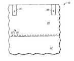
- FIG. 1Shown in FIG. 1 is a device 10 comprising a substrate 12 , a silicon oxide layer 14 , a nanocrystal 16 , a nanocrystal 18 , and a nanocrystal 20 .
- Substrate 12is a crystalline layer that may overlie an insulating material as in silicon-on-insulator (SOI) substrates.
- SOIsilicon-on-insulator
- Substrate 12is monocrystalline silicon but could be a different semiconductor material.
- Nanocrystals 16 , 18 , and 20may be formed in any one of a variety of ways. One well-known way is to deposit an amorphous silicon layer and heat it to form the nanocrystals. Another technique is to deposit the nanocrystals using chemical vapor deposition (CVD).
- CVDchemical vapor deposition
- the hemispherical shapeis considered the most desirable but a spherical shape may work just as well.
- the hemispherical shapecan be obtained by choosing an appropriate thickness of amorphous silicon and applying the heat at a temperature and time to achieve the hemispherical shape.
- the hemispherical shapemay also be obtained by appropriate CVD conditions.
- Desirably the diameter of the nanocrystalsis about 100 angstroms and the distance between nanocrystals is also about 100 angstroms.
- the 100 angstromsis a relatively short distance for a misfit dislocation to travel and should not create a threading dislocation over that distance.
- the pattern of the nanocrystalsis relatively evenly spaced apart by the nature of the processes used to form them.
- Nanocrystalsmay be formed in a variety of ways, but the particular way is not significant except that it not require a masking step in which lithography is utilized. Typical formation of a structure in an integrated circuit requires a mask that is patterned by a lithographic step. Thus, the device features are determined by the capability of the particular lithography. Thus, for example, in a 0.1-micron technology the features that can be resolved are in the order of 1000 angstroms.
- the nanocrystalsare much smaller than 1000 angstroms and the distance that they are apart, the distance to the nearest neighboring nanocrystal, is much less than 1000 angstroms. Thus, a significant improvement can be achieved by nanocrystals that are 500 Angstroms or less apart. A distance of 100 Angstroms apart is even a greater improvement. The size and distance apart of the nanocrystals may be optimized at even smaller dimensions.
- Nanocrystals 16 - 20are formed of silicon as is common in the industry.
- One typical use of nanocrystalsis to act as charge storage devices in a floating gate type non-volatile memory transistor.
- a nanocrystalis in this case considered to be a crystalline material of relatively small dimension compared to the lithographic capabilities of the current technological generation and is crystalline and substantially spherical or hemispherical in shape.
- device structure 10 of FIG. 1is known in the prior art but is generally known for its use in the formation of a memory.
- FIG. 2Shown in FIG. 2 is device structure 10 after nanocrystals 16 - 20 have been oxidized to form nanoscale islands 22 , 24 , and 26 of silicon oxide. After formation of nanoscale islands 22 - 26 there is an anisotropic etch back step to remove a portion of silicon oxide layer 14 . The result is shown in FIG. 3 with nanoscale islands 22 - 26 remaining hemispherical in shape and exposed portions of silicon substrate 12 between nanoscale islands 22 - 26 . Thus, these exposed portions of silicon substrate 12 are available for formation of an epitaxial layer on it.
- FIG. 4Shown in FIG. 4 is formation of a germanium epitaxial layer 28 over silicon substrate 12 .
- grain boundaries 30 , 32 , and 34are shown as vertical, but other orientations may result from the growth process. Additionally, as is known in the art, some or many of the grain boundaries may not even form.
- Germanium layer 28is formed with a substantially reduced number of threading dislocations because of the misfit dislocations terminating on nanoscale islands 22 - 26 . Although the dislocations can extend laterally in any direction and may not contact the nearest nanoscale island, the extension will not extend far because behind the space between two adjacent nanoscale islands will be another nanoscale island. Thus, a misfit dislocation may extend a little more than the amount the nanoscale islands are apart but not much more than that.
- FIG. 5Shown in FIG. 5 is more of device 10 that shows P-region 36 and an N-region 38 that together operate as a photo detector.
- a completed photo detectortypically would have many more P and N regions such as 36 and 38 .
- the grain boundaries 30 - 34would also be present in the additional nanoscale islands shown in FIG. 5. These are not a problem of consequence because the formation of the epitaxial layer around them comes together to form these grain boundaries at an angle with respect to each other that is low. Low angle grain boundaries have much better electrical properties than those that are not at a low angle. The low angle grain boundaries have significantly less scattering effects and fewer dangling bonds. Also many of the noncrystals may not have grain boundaries form over them.
- the resulting structure in device 10is achieved with a relatively small amount of heating and thus does not significantly effect the thermal budget of the entire integrated circuit.
- the growth of the germaniumwould be at a temperature below 600 degrees Celsius as would be the anneals of the germanium.
- the oxidation of the silicon nanocrystalsis optimally done using plasma to minimize the temperature. If a temperature above 600 degrees Celsius is used, it would be for short time periods. The temperatures and times involved are minimal compared to the very high temperatures and very long time periods that have been required to anneal out threading dislocations.
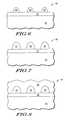
- FIG. 6Shown in FIG. 6 is a device structure 40 comprising a substrate 42 , an oxide layer 44 , nanocrystal 46 , nanocrystal 48 , and a nanocrystal 50 .
- Device structure 40 as shown in FIG. 6is similar to that shown in FIG. 1 as a starting point for an alternate embodiment to that of FIGS. 1 - 5 .
- FIG. 7Shown in FIG. 7 is device 10 after an oxidation step resulting in silicon dioxide nanoscale islands 52 , 54 , and 56 similar to that developed in FIG. 2.
- FIG. 8Shown in FIG. 8 is device 40 after deposition of a silicon nitride layer 58 over nanoscale islands 52 , 54 , and 56 .
- FIG. 9Shown in FIG. 9 is device 40 after a chemical-mechanical polishing (CMP) step in which nitride layer 58 is planarized and etched down to remove portions of nanoscale islands 52 , 54 , and 56 to form nanoscale islands 60 , 62 , and 64 .
- CMPchemical-mechanical polishing
- nanoscale islands 60 , 62 , and 64have a top surface exposed. Regions of nitride 66 , 68 , 70 , and 72 remain from nitride layer after the CMP step.
- An alternative etch back step to a CMP stepmay also be found to be effective.
- the desireis to expose the silicon oxide nanoscale islands while maintaining a material that is different from silicon oxide between the nanoscale islands.
- FIG. 10Shown in FIG. 10 is device 40 after a selective and isotropic etch of nanoscale islands 60 , 62 , and 64 . This also removes portions of oxide layer 44 that were under nanoscale islands 60 - 64 . The remaining structure is nitride regions 72 , 70 , 68 , and 66 overlying oxide portions 80 , 78 , 76 , and 74 , respectively. Oxide portions 74 - 80 are what remain after the partial removal of oxide layer 44 . There are also small portions of oxide as part of these features. These small portions of oxide are shown in FIG. 10 as portions 82 , 84 , 86 , 88 , 90 , and 92 .
- Oxide portion 82adjoins nitride portion 72 , oxide portions 84 and 86 adjoin nitride portion 70 , oxide portions 88 and 90 adjoin nitride portion 68 , and oxide portion 92 adjoins nitride portion 66 .
- portions 66 , 68 , 70 , and 72 of nitrideappear to be separated portions but they form part of a continuous layer of nitride that has holes in it.
- the nitride layerhas holes in it that are in the location where nanoscale islands 60 - 64 were present. The result is holes 81 , 83 , and 85 that expose silicon substrate 42 at those locations.
- FIG. 11Shown in FIG. 11 is device 40 after a selective epitaxial growth of germanium to result in a germanium layer 94 . Shown in FIG. 11 are grain boundaries 96 , 98 , and 100 that may be formed in various locations over the patterned nitride layer. These particular grain boundaries are shown as overlying nitride portion 70 , nitride portion 68 , and nitride portion 66 .
- FIG. 12Shown in FIG. 12 is device 40 after formation of P-type region 102 and N-type region 104 at the surface of germanium layer 94 to result in a photodetector.
- Device 40 in FIG. 12shows a greater portion of an entire integrated circuit than for FIGS. 6 - 11 .
- Shown in FIG. 12are the nitride portions 66 - 72 .
- Portions 82 , 84 , 86 , 88 , 90 , and 92 and oxide portions 74 - 80are also present but not specifically shown in FIG. 12.
- portions 66 - 72 , 74 - 80 , and 82 , 84 , 86 , 88 , 90 , and 92are an intermediate layer between the silicon substrate 42 and the epitaxial germanium layer 94 . Similar to the embodiment described for FIGS. 1 - 5 , a pattern developed from nanocrystals is utilized to form locations in the silicon substrate from which an epitaxial growth can occur. Similarly, the formation of misfit dislocations which occur at a very low height in the growth, terminate in the areas where the nitride layer remains. Thus, for example, in FIG.
- misfit dislocations formed in holes 81 , 83 , and 85would terminate in the regions where nitride portions 66 - 72 and oxide portions 74 - 80 and 82 , 84 , 86 , 88 , 90 , and 92 are present.
- the substratecould be gallium arsenide and the overlying layer could be indium phosphide or aluminum gallium arsenide.
- the underlying layercould be silicon with the overlying layer being gallium arsenide or indium phosphide.
- the silicon nanocrystalscould be an alternative material.
- An alternative that was selectively etchable to the underlying substrate materialmay not have to be converted to an oxide. In such a case, the effect is that the nanoscale islands are originally formed and not derived from nanocrystals.
- the non-lithographic pattern of material(the nanocrystals in the embodiments of the FIGS. 1 - 12 ) may not have to be separated from the substrate by a layer such as layers 14 and 44 of FIGS. 1 and 6.
Landscapes
- Engineering & Computer Science (AREA)
- Physics & Mathematics (AREA)
- Condensed Matter Physics & Semiconductors (AREA)
- General Physics & Mathematics (AREA)
- Manufacturing & Machinery (AREA)
- Computer Hardware Design (AREA)
- Microelectronics & Electronic Packaging (AREA)
- Power Engineering (AREA)
- Chemical & Material Sciences (AREA)
- Materials Engineering (AREA)
- Recrystallisation Techniques (AREA)
Abstract
Description
- 1. Field of the Invention[0001]
- This invention relates to techniques for making semiconductor devices and more particularly to forming heteroepitaxial structures.[0002]
- 2. Related Art[0003]
- There are a variety of uses in semiconductor manufacturing for heteroepitaxial structures, structures in which one type of semiconductor material is grown on the top of another type. The desire is for both the underlying semiconductor material and the overlying semiconductor material to be monocrystalline. The difficulty in this is that often the desired overlying semiconductor material has a mismatch in its crystalline structure with that of the underlying crystalline material. The problem can occur for any situation in which there are two types of semiconductor materials desired for a particular integrated circuit, but currently a typical case is for the underlying semiconductor material to be silicon because that is the most common for making integrated circuits. In the case of optical electronics, it is desirable to use germanium, which is an excellent material for use as a photodetector because of its relatively low band gap. Thus, with silicon being desirable for its use in making transistors for circuits, it would be beneficial to have a germanium layer as well as a silicon layer so that a photodetector useful for near infrared communications wavelengths (1300-1550 nanometers) can be combined with transistor circuitry on the same integrated circuit.[0004]
- Germanium and silicon, however, have crystalline structures that have a 4 percent mismatch in the lattice constant. The result of epitaxially growing a germanium layer over the silicon substrate is the formation of misfit dislocations. The misfit dislocations in turn cause threading dislocations. The threading dislocations create major problems with leakage and efficiency reduction of the photodetector. Whereas misfit dislocations remain near and parallel to the underlying substrate, threading dislocations propagate through the entire thickness of the epitaxially-grown overlying layer.[0005]
- One of the techniques that has been used to reduce the number of threading dislocations in the overlying germanium layer is to introduce an intermediate graded buffer layer between the silicon substrate and the germanium layer. The graded buffer is comprised of silicon and germanium with a local composition that can be described as Si[0006]1−xGex. During the growth of the graded buffer layer the composition starts at x=0 and gradually increases with increasing film thickness until x=1 is achieved. The change in x can either be continuous or it can be accomplished in a stepwise fashion. Following deposition of the graded buffer layer, the desired germanium layer is deposited on top of the buffer layer. This technique has been demonstrated to be able to confine a majority of the threading dislocations in the buffer layer and hence to achieve a substantial decrease in the threading dislocations in the overlying germanium layer. A disadvantage of this technique is that a thick buffer layer is required to achieve the desired decrease in threading dislocations in the overlying germanium layer. Typically the graded buffer layer needs to be approximately 10 microns thick or greater. This results in a long and expensive deposition. Additionally, the great difference in height of the silicon surface and the germanium surface will result in integration difficulties if an integrated circuit is to be fabricated from devices fabricated in the silicon surface and photodetectors in the germanium surface. Because of the disadvantages of the graded buffer technique, there have been efforts to develop alternate techniques that reduce the threading dislocations in the overlying germanium layer but with substantial reduction in thickness of any intermediate layer.
- One such technique is to provide high heat to the germanium to heal the threading dislocations. Thermal cycling to a temperature of approximately 900 degrees Celsius or above is used to cause the threading dislocations to glide. Threading dislocations can be removed from the film either by gliding to the edge of the sample or by two threading dislocations gliding together and annihilating. Longer anneal times at 900 degrees Celsius or an increased number of thermal cycles to 900 degrees Celsius have been found to reduce the density of remaining threading dislocations. Additionally, this technique has been used with mesas of germanium with restricted lateral dimensions of typically 10 to 20 microns. The germanium mesas are formed by selective growth of germanium in windows opened in a dielectric layer to expose underlying silicon. The selective germanium deposition nucleates and grows on the exposed silicon surface but not on the dielectric layer. The germanium mesas lie within the opening in the dielectric window. During the post-deposition thermal cycling, which occurs at high temperature, the restricted size of a mesa assists the gliding of threading dislocation to the dielectric layer at the edge of the mesa. This technique has been demonstrated to be beneficial in reducing threading dislocation densities, however the best reported results are not yet as good as those achieved with the graded buffer layer. The thermal cycling technique does have the advantage of achieving a reduced threading dislocation density in a thin layer of germanium. The use of multiple, high temperature thermal cycles, however, adversely affects any transistors that have already been formed in the integrated circuit. The transistors are formed with a certain amount of total heat energy that is a combination of time and temperature. This is generally known as a thermal budget. Thus, the transistors formed in the silicon portion of the integrated circuit, prior to formation of the germanium layer, have substantially used up the available thermal budget. Additional heating steps must be kept at relatively low temperature such as below 600 degrees Celsius or at least for the cases where that temperature is exceeded, it is exceeded for short time periods.[0007]
- Another technique for growth of germanium on a silicon substrate is epitaxial lateral overgrowth. In this technique, the silicon substrate is covered with an amorphous dielectric layer, (such as silicon oxide or silicon nitride), and then a pattern of openings in the dielectric layer to the underlying silicon is created using lithographic patterning processes. Selective epitaxial germanium deposition nucleates and grows over the exposed silicon regions. In the present process, however, the epitaxial germanium deposition is continued until the germanium overfills the opening in the dielectric and begins to overgrow the upper surface of the dielectric layer. The growth process is continued until the germanium material from adjacent opening meets and a continuous film is formed across the substrate. The germanium grown over the upper surface of the amorphous dielectric layer is free to assume the natural germanium lattice constant. Threading dislocations can still occur in the germanium grown directly over the silicon nucleation regions. Thermal cycling as discussed above could be used to glide the threading dislocations to the sides of the openings in the dielectric layer. Alternatively, since the threading dislocations form at 45 degrees to the silicon surface for germanium grown on (100) silicon, if the height of the opening is greater than the diameter of the opening, then the threading dislocations will terminate on the perimeter of the opening. Another aspect of epitaxial lateral overgrowth is that a seam can occur where the germanium from two adjacent nucleation sites merge. The germanium layers grown with this technique, however, can result in no defects at many seams and in twins or low angle grain boundaries at other seams that have minimal impact on the electrical properties. A disadvantage of this technique is that a thicker germanium layer must be deposited to first fill the holes and then to form the desired layer. Additionally, if the holes and spaces are relatively large, the result is a rough surface that results in the growth of the germanium from the nucleation sites. Both of these effects can be reduced by making the openings and spaces smaller. There are limitations, however, in the scaling that can be achieved with lithographic techniques.[0008]
- Thus, there is a need for forming heteroepitaxial structures in which the threading dislocations are relatively few and the heat requirements are relatively low and in which needed scaling can be achieved.[0009]
- FIG. 1 is a cross section of a device structure at a starting point of a first embodiment of the invention;[0010]
- FIGS.[0011]2-4 are cross sections of the device structure at subsequent and sequential steps according to the first embodiment of the invention;
- FIG. 5 is a cross section of the device structure of a photo detector according to a first embodiment of the invention;[0012]
- FIG. 6 is a cross section of a second device structure at a starting point for a second embodiment of the present invention;[0013]
- FIGS.[0014]7-11 are cross sections of the device structure of FIG. 6 at subsequent and sequential steps according to the second embodiment of the invention; and
- FIG. 12 is a cross section of a photo detector made according to the second embodiment of the invention.[0015]
- In one embodiment a photodetector using heteroepitaxial layers is formed in a portion of an integrated circuit using silicon nanocrystals that are formed relatively close together over a silicon substrate. These nanocrystals are completely oxidized to form insulating islands over the silicon. A subsequent etch back exposes the underlying silicon but leaves the insulating islands as masks for beginning a selective epitaxial growth of germanium over the silicon. The germanium grows and immediately forms misfit dislocations a short distance from the surface of the silicon. These misfit dislocations run a short distance above and parallel to the silicon substrate and are terminated at the insulating islands. The epitaxial growth continues and ultimately comes together at the top of these insulating islands. There may be a grain boundary formed at the top of each insulating island. The insulating islands are close enough together so that the misfit dislocations terminate on these islands prior to forming threading dislocations. This has the benefit, then, of significantly reducing the number of threading dislocations that occur while not significantly impacting the thermal budget of the whole integrated circuit. This and other embodiments are better understood by reference to the drawings and the following description.[0016]
- Shown in FIG. 1 is a[0017]
device 10 comprising asubstrate 12, asilicon oxide layer 14, ananocrystal 16, ananocrystal 18, and ananocrystal 20.Substrate 12 is a crystalline layer that may overlie an insulating material as in silicon-on-insulator (SOI) substrates.Substrate 12 is monocrystalline silicon but could be a different semiconductor material.Nanocrystals - An important aspect of the techniques for forming the nanocrystals is that they are accomplished by a non-lithographic process. Nanocrystals may be formed in a variety of ways, but the particular way is not significant except that it not require a masking step in which lithography is utilized. Typical formation of a structure in an integrated circuit requires a mask that is patterned by a lithographic step. Thus, the device features are determined by the capability of the particular lithography. Thus, for example, in a 0.1-micron technology the features that can be resolved are in the order of 1000 angstroms. The nanocrystals are much smaller than 1000 angstroms and the distance that they are apart, the distance to the nearest neighboring nanocrystal, is much less than 1000 angstroms. Thus, a significant improvement can be achieved by nanocrystals that are 500 Angstroms or less apart. A distance of 100 Angstroms apart is even a greater improvement. The size and distance apart of the nanocrystals may be optimized at even smaller dimensions.[0018]
- Nanocrystals[0019]16-20 are formed of silicon as is common in the industry. One typical use of nanocrystals is to act as charge storage devices in a floating gate type non-volatile memory transistor. Thus, a nanocrystal is in this case considered to be a crystalline material of relatively small dimension compared to the lithographic capabilities of the current technological generation and is crystalline and substantially spherical or hemispherical in shape. Thus,
device structure 10 of FIG. 1 is known in the prior art but is generally known for its use in the formation of a memory. - Shown in FIG. 2 is[0020]
device structure 10 after nanocrystals16-20 have been oxidized to formnanoscale islands silicon oxide layer 14. The result is shown in FIG. 3 with nanoscale islands22-26 remaining hemispherical in shape and exposed portions ofsilicon substrate 12 between nanoscale islands22-26. Thus, these exposed portions ofsilicon substrate 12 are available for formation of an epitaxial layer on it. - Shown in FIG. 4 is formation of a[0021]
germanium epitaxial layer 28 oversilicon substrate 12. Over nanoscale islands22-26 aregrain boundaries Germanium layer 28 is formed with a substantially reduced number of threading dislocations because of the misfit dislocations terminating on nanoscale islands22-26. Although the dislocations can extend laterally in any direction and may not contact the nearest nanoscale island, the extension will not extend far because behind the space between two adjacent nanoscale islands will be another nanoscale island. Thus, a misfit dislocation may extend a little more than the amount the nanoscale islands are apart but not much more than that. - Shown in FIG. 5 is more of[0022]
device 10 that shows P-region 36 and an N-region 38 that together operate as a photo detector. A completed photo detector typically would have many more P and N regions such as36 and38. The grain boundaries30-34 would also be present in the additional nanoscale islands shown in FIG. 5. These are not a problem of consequence because the formation of the epitaxial layer around them comes together to form these grain boundaries at an angle with respect to each other that is low. Low angle grain boundaries have much better electrical properties than those that are not at a low angle. The low angle grain boundaries have significantly less scattering effects and fewer dangling bonds. Also many of the noncrystals may not have grain boundaries form over them. - The resulting structure in[0023]
device 10 is achieved with a relatively small amount of heating and thus does not significantly effect the thermal budget of the entire integrated circuit. The growth of the germanium would be at a temperature below 600 degrees Celsius as would be the anneals of the germanium. The oxidation of the silicon nanocrystals is optimally done using plasma to minimize the temperature. If a temperature above 600 degrees Celsius is used, it would be for short time periods. The temperatures and times involved are minimal compared to the very high temperatures and very long time periods that have been required to anneal out threading dislocations. - Shown in FIG. 6 is a[0024]
device structure 40 comprising asubstrate 42, anoxide layer 44,nanocrystal 46,nanocrystal 48, and ananocrystal 50.Device structure 40 as shown in FIG. 6 is similar to that shown in FIG. 1 as a starting point for an alternate embodiment to that of FIGS.1-5. - Shown in FIG. 7 is[0025]
device 10 after an oxidation step resulting in silicon dioxidenanoscale islands device 40 after deposition of asilicon nitride layer 58 overnanoscale islands - Shown in FIG. 9 is[0026]
device 40 after a chemical-mechanical polishing (CMP) step in which nitridelayer 58 is planarized and etched down to remove portions ofnanoscale islands nanoscale islands nanoscale islands nitride - Shown in FIG. 10 is[0027]
device 40 after a selective and isotropic etch ofnanoscale islands oxide layer 44 that were under nanoscale islands60-64. The remaining structure isnitride regions overlying oxide portions oxide layer 44. There are also small portions of oxide as part of these features. These small portions of oxide are shown in FIG. 10 asportions Oxide portion 82 adjoinsnitride portion 72,oxide portions adjoin nitride portion 70,oxide portions adjoin nitride portion 68, andoxide portion 92 adjoinsnitride portion 66. In this cross section shown in FIG. 10,portions holes silicon substrate 42 at those locations. - Shown in FIG. 11 is[0028]
device 40 after a selective epitaxial growth of germanium to result in agermanium layer 94. Shown in FIG. 11 aregrain boundaries overlying nitride portion 70,nitride portion 68, andnitride portion 66. - Shown in FIG. 12 is[0029]
device 40 after formation of P-type region 102 and N-type region 104 at the surface ofgermanium layer 94 to result in a photodetector.Device 40 in FIG. 12 shows a greater portion of an entire integrated circuit than for FIGS.6-11. Shown in FIG. 12 are the nitride portions66-72.Portions silicon substrate 42 and theepitaxial germanium layer 94. Similar to the embodiment described for FIGS.1-5, a pattern developed from nanocrystals is utilized to form locations in the silicon substrate from which an epitaxial growth can occur. Similarly, the formation of misfit dislocations which occur at a very low height in the growth, terminate in the areas where the nitride layer remains. Thus, for example, in FIG. 11 the misfit dislocations formed inholes - Although the description has been for selective epitaxial deposition of germanium on silicon because of particular benefits of that combination, there may other alternatives as well. For example, the substrate could be gallium arsenide and the overlying layer could be indium phosphide or aluminum gallium arsenide. Also the underlying layer could be silicon with the overlying layer being gallium arsenide or indium phosphide. Similarly, the silicon nanocrystals could be an alternative material. An alternative that was selectively etchable to the underlying substrate material may not have to be converted to an oxide. In such a case, the effect is that the nanoscale islands are originally formed and not derived from nanocrystals. Also, the non-lithographic pattern of material (the nanocrystals in the embodiments of the FIGS.[0030]1-12) may not have to be separated from the substrate by a layer such as
layers - Benefits, other advantages, and solutions to problems have been described above with regard to specific embodiments. However, the benefits, advantages, solutions to problems, and any element(s) that may cause any benefit, advantage, or solution to occur or become more pronounced are not to be construed as a critical, required, or essential feature or element of any or all the claims. As used herein, the terms “comprises,” “comprising,” or any other variation thereof, are intended to cover a non-exclusive inclusion, such that a process, method, article, or apparatus that comprises a list of elements does not include only those elements but may include other elements not expressly listed.[0031]
Claims (24)
Priority Applications (1)
| Application Number | Priority Date | Filing Date | Title |
|---|---|---|---|
| US09/997,886US6576532B1 (en) | 2001-11-30 | 2001-11-30 | Semiconductor device and method therefor |
Applications Claiming Priority (1)
| Application Number | Priority Date | Filing Date | Title |
|---|---|---|---|
| US09/997,886US6576532B1 (en) | 2001-11-30 | 2001-11-30 | Semiconductor device and method therefor |
Publications (2)
| Publication Number | Publication Date |
|---|---|
| US20030102469A1true US20030102469A1 (en) | 2003-06-05 |
| US6576532B1 US6576532B1 (en) | 2003-06-10 |
Family
ID=25544517
Family Applications (1)
| Application Number | Title | Priority Date | Filing Date |
|---|---|---|---|
| US09/997,886Expired - LifetimeUS6576532B1 (en) | 2001-11-30 | 2001-11-30 | Semiconductor device and method therefor |
Country Status (1)
| Country | Link |
|---|---|
| US (1) | US6576532B1 (en) |
Cited By (16)
| Publication number | Priority date | Publication date | Assignee | Title |
|---|---|---|---|---|
| US20050042823A1 (en)* | 2003-08-18 | 2005-02-24 | Shenlin Chen | Hemi-spherical grain silicon enhancement |
| US20050054180A1 (en)* | 2003-09-09 | 2005-03-10 | Sang Han | Threading-dislocation-free nanoheteroepitaxy of Ge on Si using self-directed touch-down of Ge through a thin SiO2 layer |
| US20050184354A1 (en)* | 2004-02-24 | 2005-08-25 | International Business Machines Corporation | Structure for and method of fabricating a high-speed CMOS-compatible Ge-on-insulator photodetector |
| US20050205954A1 (en)* | 2002-12-18 | 2005-09-22 | King Clifford A | Image sensor comprising isolated germanium photodetectors integrated with a silicon substrate and silicon circuitry |
| US20060073681A1 (en)* | 2004-09-08 | 2006-04-06 | Han Sang M | Nanoheteroepitaxy of Ge on Si as a foundation for group III-V and II-VI integration |
| US7105425B1 (en)* | 2002-05-16 | 2006-09-12 | Advanced Micro Devices, Inc. | Single electron devices formed by laser thermal annealing |
| WO2006047645A3 (en)* | 2004-10-25 | 2007-06-07 | Scott H Heneveld Sr | Expandable implant for repairing a defective intervertebral nucleus |
| US20070290188A1 (en)* | 2006-06-16 | 2007-12-20 | Industrial Technology Research Institute | Semiconductor light emitting device substrate and method of fabricating the same |
| US20110215407A1 (en)* | 2010-03-02 | 2011-09-08 | Micron Technology, Inc. | Semiconductor-metal-on-insulator structures, methods of forming such structures, and semiconductor devices including such structures |
| WO2012058264A1 (en)* | 2010-10-26 | 2012-05-03 | The Regents Of The University Of California | Limiting strain relaxation in iii-nitride heterostructures by substrate and epitaxial layer patterning |
| US9343462B2 (en) | 2010-03-02 | 2016-05-17 | Micron Technology, Inc. | Thyristor-based memory cells, devices and systems including the same and methods for forming the same |
| US9361966B2 (en) | 2011-03-08 | 2016-06-07 | Micron Technology, Inc. | Thyristors |
| US9646869B2 (en) | 2010-03-02 | 2017-05-09 | Micron Technology, Inc. | Semiconductor devices including a diode structure over a conductive strap and methods of forming such semiconductor devices |
| CN107924961A (en)* | 2015-08-28 | 2018-04-17 | 日本电信电话株式会社 | Photodetector |
| US10157769B2 (en) | 2010-03-02 | 2018-12-18 | Micron Technology, Inc. | Semiconductor devices including a diode structure over a conductive strap and methods of forming such semiconductor devices |
| US10373956B2 (en) | 2011-03-01 | 2019-08-06 | Micron Technology, Inc. | Gated bipolar junction transistors, memory arrays, and methods of forming gated bipolar junction transistors |
Families Citing this family (36)
| Publication number | Priority date | Publication date | Assignee | Title |
|---|---|---|---|---|
| JP2003520444A (en)* | 2000-01-20 | 2003-07-02 | アンバーウェーブ システムズ コーポレイション | Low threading dislocation density lattice-mismatched epilayer that does not require high-temperature growth |
| AU2003261300A1 (en)* | 2002-07-29 | 2004-02-16 | Amberwave Systems | Selective placement of dislocation arrays |
| AU2003274922A1 (en)* | 2002-08-23 | 2004-03-11 | Amberwave Systems Corporation | Semiconductor heterostructures having reduced dislocation pile-ups and related methods |
| US7594967B2 (en) | 2002-08-30 | 2009-09-29 | Amberwave Systems Corporation | Reduction of dislocation pile-up formation during relaxed lattice-mismatched epitaxy |
| JP4659732B2 (en) | 2003-01-27 | 2011-03-30 | 台湾積體電路製造股▲ふん▼有限公司 | Method for forming a semiconductor layer |
| US6982229B2 (en)* | 2003-04-18 | 2006-01-03 | Lsi Logic Corporation | Ion recoil implantation and enhanced carrier mobility in CMOS device |
| US20040206951A1 (en)* | 2003-04-18 | 2004-10-21 | Mirabedini Mohammad R. | Ion implantation in channel region of CMOS device for enhanced carrier mobility |
| US7279369B2 (en)* | 2003-08-21 | 2007-10-09 | Intel Corporation | Germanium on insulator fabrication via epitaxial germanium bonding |
| EP2595175B1 (en)* | 2005-05-17 | 2019-04-17 | Taiwan Semiconductor Manufacturing Company, Ltd. | Method of fabricating a lattice-mismatched semiconductor structure with reduced dislocation defect densities |
| US8324660B2 (en) | 2005-05-17 | 2012-12-04 | Taiwan Semiconductor Manufacturing Company, Ltd. | Lattice-mismatched semiconductor structures with reduced dislocation defect densities and related methods for device fabrication |
| US20070267722A1 (en)* | 2006-05-17 | 2007-11-22 | Amberwave Systems Corporation | Lattice-mismatched semiconductor structures with reduced dislocation defect densities and related methods for device fabrication |
| US9153645B2 (en) | 2005-05-17 | 2015-10-06 | Taiwan Semiconductor Manufacturing Company, Ltd. | Lattice-mismatched semiconductor structures with reduced dislocation defect densities and related methods for device fabrication |
| KR101329388B1 (en) | 2005-07-26 | 2013-11-14 | 앰버웨이브 시스템즈 코포레이션 | Solutions for integrated circuit integration of alternative active area materials |
| US20070054467A1 (en)* | 2005-09-07 | 2007-03-08 | Amberwave Systems Corporation | Methods for integrating lattice-mismatched semiconductor structure on insulators |
| US7638842B2 (en)* | 2005-09-07 | 2009-12-29 | Amberwave Systems Corporation | Lattice-mismatched semiconductor structures on insulators |
| US7241695B2 (en)* | 2005-10-06 | 2007-07-10 | Freescale Semiconductor, Inc. | Semiconductor device having nano-pillars and method therefor |
| WO2007112066A2 (en) | 2006-03-24 | 2007-10-04 | Amberwave Systems Corporation | Lattice-mismatched semiconductor structures and related methods for device fabrication |
| US20070262296A1 (en)* | 2006-05-11 | 2007-11-15 | Matthias Bauer | Photodetectors employing germanium layers |
| US8173551B2 (en) | 2006-09-07 | 2012-05-08 | Taiwan Semiconductor Manufacturing Co., Ltd. | Defect reduction using aspect ratio trapping |
| US20080070355A1 (en)* | 2006-09-18 | 2008-03-20 | Amberwave Systems Corporation | Aspect ratio trapping for mixed signal applications |
| WO2008039495A1 (en) | 2006-09-27 | 2008-04-03 | Amberwave Systems Corporation | Tri-gate field-effect transistors formed by aspect ratio trapping |
| WO2008039534A2 (en) | 2006-09-27 | 2008-04-03 | Amberwave Systems Corporation | Quantum tunneling devices and circuits with lattice- mismatched semiconductor structures |
| US8502263B2 (en) | 2006-10-19 | 2013-08-06 | Taiwan Semiconductor Manufacturing Company, Ltd. | Light-emitter-based devices with lattice-mismatched semiconductor structures |
| US7825328B2 (en) | 2007-04-09 | 2010-11-02 | Taiwan Semiconductor Manufacturing Company, Ltd. | Nitride-based multi-junction solar cell modules and methods for making the same |
| US8237151B2 (en) | 2009-01-09 | 2012-08-07 | Taiwan Semiconductor Manufacturing Company, Ltd. | Diode-based devices and methods for making the same |
| US8304805B2 (en) | 2009-01-09 | 2012-11-06 | Taiwan Semiconductor Manufacturing Company, Ltd. | Semiconductor diodes fabricated by aspect ratio trapping with coalesced films |
| WO2008124154A2 (en) | 2007-04-09 | 2008-10-16 | Amberwave Systems Corporation | Photovoltaics on silicon |
| US8329541B2 (en) | 2007-06-15 | 2012-12-11 | Taiwan Semiconductor Manufacturing Company, Ltd. | InP-based transistor fabrication |
| JP2010538495A (en) | 2007-09-07 | 2010-12-09 | アンバーウェーブ・システムズ・コーポレーション | Multi-junction solar cell |
| US8183667B2 (en) | 2008-06-03 | 2012-05-22 | Taiwan Semiconductor Manufacturing Co., Ltd. | Epitaxial growth of crystalline material |
| US8274097B2 (en) | 2008-07-01 | 2012-09-25 | Taiwan Semiconductor Manufacturing Company, Ltd. | Reduction of edge effects from aspect ratio trapping |
| US8981427B2 (en) | 2008-07-15 | 2015-03-17 | Taiwan Semiconductor Manufacturing Company, Ltd. | Polishing of small composite semiconductor materials |
| US20100072515A1 (en) | 2008-09-19 | 2010-03-25 | Amberwave Systems Corporation | Fabrication and structures of crystalline material |
| EP2335273A4 (en)* | 2008-09-19 | 2012-01-25 | Taiwan Semiconductor Mfg | FORMATION OF DEVICES BY GROWTH OF EPITAXIAL LAYERS |
| US8253211B2 (en) | 2008-09-24 | 2012-08-28 | Taiwan Semiconductor Manufacturing Company, Ltd. | Semiconductor sensor structures with reduced dislocation defect densities |
| US8629446B2 (en) | 2009-04-02 | 2014-01-14 | Taiwan Semiconductor Manufacturing Company, Ltd. | Devices formed from a non-polar plane of a crystalline material and method of making the same |
Family Cites Families (6)
| Publication number | Priority date | Publication date | Assignee | Title |
|---|---|---|---|---|
| US4174422A (en)* | 1977-12-30 | 1979-11-13 | International Business Machines Corporation | Growing epitaxial films when the misfit between film and substrate is large |
| US6060743A (en)* | 1997-05-21 | 2000-05-09 | Kabushiki Kaisha Toshiba | Semiconductor memory device having multilayer group IV nanocrystal quantum dot floating gate and method of manufacturing the same |
| JP3036495B2 (en)* | 1997-11-07 | 2000-04-24 | 豊田合成株式会社 | Method for manufacturing gallium nitride-based compound semiconductor |
| JP3403076B2 (en)* | 1998-06-30 | 2003-05-06 | 株式会社東芝 | Semiconductor device and manufacturing method thereof |
| DE60039875D1 (en) | 1999-06-25 | 2008-09-25 | Massachusetts Inst Technology | CYCLIC THERMAL HEALING METHOD FOR REDUCING CRYSTAL TRANSLATION |
| JP3603713B2 (en)* | 1999-12-27 | 2004-12-22 | 豊田合成株式会社 | Method of growing group III nitride compound semiconductor film and group III nitride compound semiconductor device |
- 2001
- 2001-11-30USUS09/997,886patent/US6576532B1/ennot_activeExpired - Lifetime
Cited By (41)
| Publication number | Priority date | Publication date | Assignee | Title |
|---|---|---|---|---|
| US7105425B1 (en)* | 2002-05-16 | 2006-09-12 | Advanced Micro Devices, Inc. | Single electron devices formed by laser thermal annealing |
| US8664739B2 (en) | 2002-12-18 | 2014-03-04 | Infrared Newco, Inc. | Image sensor comprising isolated germanium photodetectors integrated with a silicon substrate and silicon circuitry |
| US7453129B2 (en)* | 2002-12-18 | 2008-11-18 | Noble Peak Vision Corp. | Image sensor comprising isolated germanium photodetectors integrated with a silicon substrate and silicon circuitry |
| US20050205954A1 (en)* | 2002-12-18 | 2005-09-22 | King Clifford A | Image sensor comprising isolated germanium photodetectors integrated with a silicon substrate and silicon circuitry |
| US20090072284A1 (en)* | 2002-12-18 | 2009-03-19 | Noble Peak Vision Corp. | Image sensor comprising isolated germanium photodetectors integrated with a silicon substrate and silicon circuitry |
| US7973377B2 (en) | 2002-12-18 | 2011-07-05 | Infrared Newco, Inc. | Image sensor comprising isolated germanium photodetectors integrated with a silicon substrate and silicon circuitry |
| US9142585B2 (en) | 2002-12-18 | 2015-09-22 | Infrared Newco, Inc. | Image sensor comprising isolated germanium photodetectors integrated with a silicon substrate and silicon circuitry |
| US20050176213A1 (en)* | 2003-08-18 | 2005-08-11 | Shenlin Chen | Hemi-spherical grain silicon enhancement |
| US20050042823A1 (en)* | 2003-08-18 | 2005-02-24 | Shenlin Chen | Hemi-spherical grain silicon enhancement |
| US6902973B2 (en)* | 2003-08-18 | 2005-06-07 | Micron Technology, Inc. | Hemi-spherical grain silicon enhancement |
| US7888244B2 (en) | 2003-09-09 | 2011-02-15 | Stc.Unm | Threading-dislocation-free nanoheteroepitaxy of Ge on Si using self-directed touch-down of Ge through a thin SiO2 layer |
| US7579263B2 (en)* | 2003-09-09 | 2009-08-25 | Stc.Unm | Threading-dislocation-free nanoheteroepitaxy of Ge on Si using self-directed touch-down of Ge through a thin SiO2 layer |
| US20050054180A1 (en)* | 2003-09-09 | 2005-03-10 | Sang Han | Threading-dislocation-free nanoheteroepitaxy of Ge on Si using self-directed touch-down of Ge through a thin SiO2 layer |
| US20080185618A1 (en)* | 2004-02-24 | 2008-08-07 | International Business Machines Corporation | STRUCTURE FOR AND METHOD OF FABRICATING A HIGH-SPEED CMOS-COMPATIBLE Ge-ON-INSULATOR PHOTODETECTOR |
| US20080113467A1 (en)* | 2004-02-24 | 2008-05-15 | International Business Machines Corporation | STRUCTURE FOR AND METHOD OF FABRICATING A HIGH-SPEED CMOS-COMPATIBLE Ge-ON-INSULATOR PHOTODETECTOR |
| US7138697B2 (en)* | 2004-02-24 | 2006-11-21 | International Business Machines Corporation | Structure for and method of fabricating a high-speed CMOS-compatible Ge-on-insulator photodetector |
| US7510904B2 (en) | 2004-02-24 | 2009-03-31 | International Business Machines Corporation | Structure for and method of fabricating a high-speed CMOS-compatible Ge-on-insulator photodetector |
| KR100951226B1 (en) | 2004-02-24 | 2010-04-05 | 인터내셔널 비지네스 머신즈 코포레이션 | Structure and method for manufacturing germanium-on-insulator photodetector suitable for high speed COS |
| US20050184354A1 (en)* | 2004-02-24 | 2005-08-25 | International Business Machines Corporation | Structure for and method of fabricating a high-speed CMOS-compatible Ge-on-insulator photodetector |
| US7915653B2 (en) | 2004-02-24 | 2011-03-29 | International Business Machines Corporation | Structure for and method of fabricating a high-speed CMOS-compatible Ge-on-insulator photodetector |
| US20060073681A1 (en)* | 2004-09-08 | 2006-04-06 | Han Sang M | Nanoheteroepitaxy of Ge on Si as a foundation for group III-V and II-VI integration |
| WO2006047645A3 (en)* | 2004-10-25 | 2007-06-07 | Scott H Heneveld Sr | Expandable implant for repairing a defective intervertebral nucleus |
| US20070290188A1 (en)* | 2006-06-16 | 2007-12-20 | Industrial Technology Research Institute | Semiconductor light emitting device substrate and method of fabricating the same |
| US20080305571A1 (en)* | 2006-06-16 | 2008-12-11 | Industrial Technology Research Institute | Method of fabricating semiconductor light emitting device substrate |
| US7427772B2 (en)* | 2006-06-16 | 2008-09-23 | Industrial Technology Research Institute | Semiconductor light emitting device substrate and method of fabricating the same |
| US9608119B2 (en)* | 2010-03-02 | 2017-03-28 | Micron Technology, Inc. | Semiconductor-metal-on-insulator structures, methods of forming such structures, and semiconductor devices including such structures |
| US10325926B2 (en) | 2010-03-02 | 2019-06-18 | Micron Technology, Inc. | Semiconductor-metal-on-insulator structures, methods of forming such structures, and semiconductor devices including such structures |
| US10157769B2 (en) | 2010-03-02 | 2018-12-18 | Micron Technology, Inc. | Semiconductor devices including a diode structure over a conductive strap and methods of forming such semiconductor devices |
| US20110215407A1 (en)* | 2010-03-02 | 2011-09-08 | Micron Technology, Inc. | Semiconductor-metal-on-insulator structures, methods of forming such structures, and semiconductor devices including such structures |
| US9343462B2 (en) | 2010-03-02 | 2016-05-17 | Micron Technology, Inc. | Thyristor-based memory cells, devices and systems including the same and methods for forming the same |
| US9646869B2 (en) | 2010-03-02 | 2017-05-09 | Micron Technology, Inc. | Semiconductor devices including a diode structure over a conductive strap and methods of forming such semiconductor devices |
| US8853669B2 (en) | 2010-10-26 | 2014-10-07 | The Regents Of The University Of California | Limiting strain relaxation in III-nitride hetero-structures by substrate and epitaxial layer patterning |
| CN103190041A (en)* | 2010-10-26 | 2013-07-03 | 加利福尼亚大学董事会 | Limiting strain relaxation in III-nitride heterostructures by substrate and epitaxial layer patterning |
| WO2012058264A1 (en)* | 2010-10-26 | 2012-05-03 | The Regents Of The University Of California | Limiting strain relaxation in iii-nitride heterostructures by substrate and epitaxial layer patterning |
| US10373956B2 (en) | 2011-03-01 | 2019-08-06 | Micron Technology, Inc. | Gated bipolar junction transistors, memory arrays, and methods of forming gated bipolar junction transistors |
| US10886273B2 (en) | 2011-03-01 | 2021-01-05 | Micron Technology, Inc. | Gated bipolar junction transistors, memory arrays, and methods of forming gated bipolar junction transistors |
| US9361966B2 (en) | 2011-03-08 | 2016-06-07 | Micron Technology, Inc. | Thyristors |
| US9691465B2 (en) | 2011-03-08 | 2017-06-27 | Micron Technology, Inc. | Thyristors, methods of programming thyristors, and methods of forming thyristors |
| CN107924961A (en)* | 2015-08-28 | 2018-04-17 | 日本电信电话株式会社 | Photodetector |
| JP2018142751A (en)* | 2015-08-28 | 2018-09-13 | 日本電信電話株式会社 | Photodetector |
| US10720543B2 (en)* | 2015-08-28 | 2020-07-21 | Nippon Telegraph And Telephone Corporation | Photodetector |
Also Published As
| Publication number | Publication date |
|---|---|
| US6576532B1 (en) | 2003-06-10 |
Similar Documents
| Publication | Publication Date | Title |
|---|---|---|
| US6576532B1 (en) | Semiconductor device and method therefor | |
| US11251272B2 (en) | Lattice-mismatched semiconductor structures with reduced dislocation defect densities and related methods for device fabrication | |
| EP2528087B1 (en) | Formation of devices by epitaxial layer overgrowth | |
| US11342441B2 (en) | Method of forming a seed area and growing a heteroepitaxial layer on the seed area | |
| KR101115091B1 (en) | Semiconductor structure with different lattice constant materials and method for forming the same | |
| JPS5893221A (en) | Semiconductor thin film structure and preparation thereof | |
| JP2011082526A (en) | Method of growing group iii-v layer on silicon using nano-scale orientation pattern | |
| EP0501119B1 (en) | Method of producing semiconductor substrate | |
| JPH10256169A (en) | Manufacture of semiconductor device | |
| US7235809B2 (en) | Semiconductor channel on insulator structure | |
| US5341000A (en) | Thin silicon carbide layer on an insulating layer | |
| US5402989A (en) | Method for manufacturing semiconductor device having grown layer on insulating layer | |
| JP2008027969A (en) | Manufacturing method of single crystal wafer | |
| US6633056B2 (en) | Hetero-integration of dissimilar semiconductor materials | |
| JPH03292723A (en) | Manufacture of silicon singe crystal thin film | |
| JP4221928B2 (en) | Semiconductor substrate, field effect transistor, and manufacturing method thereof | |
| JP4254102B2 (en) | Semiconductor substrate, field effect transistor, and manufacturing method thereof | |
| JPH0546706B2 (en) | ||
| JP2527227B2 (en) | Semiconductor device and manufacturing method thereof | |
| KR20050024669A (en) | Semiconductor wafer having guardring layer and method for manufacturing the same | |
| KR19980043236A (en) | Selective single crystal thin film growth method without crystal defect and slope |
Legal Events
| Date | Code | Title | Description |
|---|---|---|---|
| AS | Assignment | Owner name:MOTOROLA, INC., ILLINOIS Free format text:ASSIGNMENT OF ASSIGNORS INTEREST;ASSIGNORS:JONES, ROBERT E.;WHITE, BRUCE E.;REEL/FRAME:012337/0705 Effective date:20011129 | |
| STCF | Information on status: patent grant | Free format text:PATENTED CASE | |
| AS | Assignment | Owner name:FREESCALE SEMICONDUCTOR, INC., TEXAS Free format text:ASSIGNMENT OF ASSIGNORS INTEREST;ASSIGNOR:MOTOROLA, INC.;REEL/FRAME:015698/0657 Effective date:20040404 Owner name:FREESCALE SEMICONDUCTOR, INC.,TEXAS Free format text:ASSIGNMENT OF ASSIGNORS INTEREST;ASSIGNOR:MOTOROLA, INC.;REEL/FRAME:015698/0657 Effective date:20040404 | |
| FPAY | Fee payment | Year of fee payment:4 | |
| AS | Assignment | Owner name:CITIBANK, N.A. AS COLLATERAL AGENT, NEW YORK Free format text:SECURITY AGREEMENT;ASSIGNORS:FREESCALE SEMICONDUCTOR, INC.;FREESCALE ACQUISITION CORPORATION;FREESCALE ACQUISITION HOLDINGS CORP.;AND OTHERS;REEL/FRAME:018855/0129 Effective date:20061201 Owner name:CITIBANK, N.A. AS COLLATERAL AGENT,NEW YORK Free format text:SECURITY AGREEMENT;ASSIGNORS:FREESCALE SEMICONDUCTOR, INC.;FREESCALE ACQUISITION CORPORATION;FREESCALE ACQUISITION HOLDINGS CORP.;AND OTHERS;REEL/FRAME:018855/0129 Effective date:20061201 | |
| AS | Assignment | Owner name:CITIBANK, N.A., AS COLLATERAL AGENT,NEW YORK Free format text:SECURITY AGREEMENT;ASSIGNOR:FREESCALE SEMICONDUCTOR, INC.;REEL/FRAME:024397/0001 Effective date:20100413 Owner name:CITIBANK, N.A., AS COLLATERAL AGENT, NEW YORK Free format text:SECURITY AGREEMENT;ASSIGNOR:FREESCALE SEMICONDUCTOR, INC.;REEL/FRAME:024397/0001 Effective date:20100413 | |
| FPAY | Fee payment | Year of fee payment:8 | |
| AS | Assignment | Owner name:CITIBANK, N.A., AS NOTES COLLATERAL AGENT, NEW YORK Free format text:SECURITY AGREEMENT;ASSIGNOR:FREESCALE SEMICONDUCTOR, INC.;REEL/FRAME:030633/0424 Effective date:20130521 Owner name:CITIBANK, N.A., AS NOTES COLLATERAL AGENT, NEW YOR Free format text:SECURITY AGREEMENT;ASSIGNOR:FREESCALE SEMICONDUCTOR, INC.;REEL/FRAME:030633/0424 Effective date:20130521 | |
| AS | Assignment | Owner name:CITIBANK, N.A., AS NOTES COLLATERAL AGENT, NEW YORK Free format text:SECURITY AGREEMENT;ASSIGNOR:FREESCALE SEMICONDUCTOR, INC.;REEL/FRAME:031591/0266 Effective date:20131101 Owner name:CITIBANK, N.A., AS NOTES COLLATERAL AGENT, NEW YOR Free format text:SECURITY AGREEMENT;ASSIGNOR:FREESCALE SEMICONDUCTOR, INC.;REEL/FRAME:031591/0266 Effective date:20131101 | |
| FPAY | Fee payment | Year of fee payment:12 | |
| AS | Assignment | Owner name:FREESCALE SEMICONDUCTOR, INC., TEXAS Free format text:PATENT RELEASE;ASSIGNOR:CITIBANK, N.A., AS COLLATERAL AGENT;REEL/FRAME:037356/0553 Effective date:20151207 Owner name:FREESCALE SEMICONDUCTOR, INC., TEXAS Free format text:PATENT RELEASE;ASSIGNOR:CITIBANK, N.A., AS COLLATERAL AGENT;REEL/FRAME:037354/0225 Effective date:20151207 Owner name:FREESCALE SEMICONDUCTOR, INC., TEXAS Free format text:PATENT RELEASE;ASSIGNOR:CITIBANK, N.A., AS COLLATERAL AGENT;REEL/FRAME:037356/0143 Effective date:20151207 | |
| AS | Assignment | Owner name:MORGAN STANLEY SENIOR FUNDING, INC., MARYLAND Free format text:ASSIGNMENT AND ASSUMPTION OF SECURITY INTEREST IN PATENTS;ASSIGNOR:CITIBANK, N.A.;REEL/FRAME:037486/0517 Effective date:20151207 | |
| AS | Assignment | Owner name:MORGAN STANLEY SENIOR FUNDING, INC., MARYLAND Free format text:ASSIGNMENT AND ASSUMPTION OF SECURITY INTEREST IN PATENTS;ASSIGNOR:CITIBANK, N.A.;REEL/FRAME:037518/0292 Effective date:20151207 | |
| AS | Assignment | Owner name:NORTH STAR INNOVATIONS INC., CALIFORNIA Free format text:ASSIGNMENT OF ASSIGNORS INTEREST;ASSIGNOR:FREESCALE SEMICONDUCTOR, INC.;REEL/FRAME:037694/0264 Effective date:20151002 | |
| AS | Assignment | Owner name:NXP, B.V., F/K/A FREESCALE SEMICONDUCTOR, INC., NETHERLANDS Free format text:RELEASE BY SECURED PARTY;ASSIGNOR:MORGAN STANLEY SENIOR FUNDING, INC.;REEL/FRAME:040925/0001 Effective date:20160912 Owner name:NXP, B.V., F/K/A FREESCALE SEMICONDUCTOR, INC., NE Free format text:RELEASE BY SECURED PARTY;ASSIGNOR:MORGAN STANLEY SENIOR FUNDING, INC.;REEL/FRAME:040925/0001 Effective date:20160912 | |
| AS | Assignment | Owner name:NXP B.V., NETHERLANDS Free format text:RELEASE BY SECURED PARTY;ASSIGNOR:MORGAN STANLEY SENIOR FUNDING, INC.;REEL/FRAME:040928/0001 Effective date:20160622 | |
| AS | Assignment | Owner name:MORGAN STANLEY SENIOR FUNDING, INC., MARYLAND Free format text:CORRECTIVE ASSIGNMENT TO CORRECT THE REMOVE PATENTS 8108266 AND 8062324 AND REPLACE THEM WITH 6108266 AND 8060324 PREVIOUSLY RECORDED ON REEL 037518 FRAME 0292. ASSIGNOR(S) HEREBY CONFIRMS THE ASSIGNMENT AND ASSUMPTION OF SECURITY INTEREST IN PATENTS;ASSIGNOR:CITIBANK, N.A.;REEL/FRAME:041703/0536 Effective date:20151207 | |
| AS | Assignment | Owner name:SHENZHEN XINGUODU TECHNOLOGY CO., LTD., CHINA Free format text:CORRECTIVE ASSIGNMENT TO CORRECT THE TO CORRECT THE APPLICATION NO. FROM 13,883,290 TO 13,833,290 PREVIOUSLY RECORDED ON REEL 041703 FRAME 0536. ASSIGNOR(S) HEREBY CONFIRMS THE THE ASSIGNMENT AND ASSUMPTION OF SECURITYINTEREST IN PATENTS.;ASSIGNOR:MORGAN STANLEY SENIOR FUNDING, INC.;REEL/FRAME:048734/0001 Effective date:20190217 | |
| AS | Assignment | Owner name:MORGAN STANLEY SENIOR FUNDING, INC., MARYLAND Free format text:CORRECTIVE ASSIGNMENT TO CORRECT THE REMOVE APPLICATION11759915 AND REPLACE IT WITH APPLICATION 11759935 PREVIOUSLY RECORDED ON REEL 037486 FRAME 0517. ASSIGNOR(S) HEREBY CONFIRMS THE ASSIGNMENT AND ASSUMPTION OF SECURITYINTEREST IN PATENTS;ASSIGNOR:CITIBANK, N.A.;REEL/FRAME:053547/0421 Effective date:20151207 | |
| AS | Assignment | Owner name:NXP B.V., NETHERLANDS Free format text:CORRECTIVE ASSIGNMENT TO CORRECT THE REMOVEAPPLICATION 11759915 AND REPLACE IT WITH APPLICATION11759935 PREVIOUSLY RECORDED ON REEL 040928 FRAME 0001. ASSIGNOR(S) HEREBY CONFIRMS THE RELEASE OF SECURITYINTEREST;ASSIGNOR:MORGAN STANLEY SENIOR FUNDING, INC.;REEL/FRAME:052915/0001 Effective date:20160622 | |
| AS | Assignment | Owner name:NXP, B.V. F/K/A FREESCALE SEMICONDUCTOR, INC., NETHERLANDS Free format text:CORRECTIVE ASSIGNMENT TO CORRECT THE REMOVEAPPLICATION 11759915 AND REPLACE IT WITH APPLICATION11759935 PREVIOUSLY RECORDED ON REEL 040925 FRAME 0001. ASSIGNOR(S) HEREBY CONFIRMS THE RELEASE OF SECURITYINTEREST;ASSIGNOR:MORGAN STANLEY SENIOR FUNDING, INC.;REEL/FRAME:052917/0001 Effective date:20160912 |