US20030095426A1 - Complementary bit PCRAM sense amplifier and method of operation - Google Patents
Complementary bit PCRAM sense amplifier and method of operationDownload PDFInfo
- Publication number
- US20030095426A1 US20030095426A1US09/988,627US98862701AUS2003095426A1US 20030095426 A1US20030095426 A1US 20030095426A1US 98862701 AUS98862701 AUS 98862701AUS 2003095426 A1US2003095426 A1US 2003095426A1
- Authority
- US
- United States
- Prior art keywords
- memory
- voltage
- memory elements
- digit lines
- lines
- Prior art date
- Legal status (The legal status is an assumption and is not a legal conclusion. Google has not performed a legal analysis and makes no representation as to the accuracy of the status listed.)
- Granted
Links
- 230000000295complement effectEffects0.000titleclaimsabstractdescription23
- 238000000034methodMethods0.000titleclaimsabstractdescription22
- 239000004020conductorSubstances0.000claimsabstractdescription26
- 238000007599dischargingMethods0.000claimsabstractdescription13
- 230000003071parasitic effectEffects0.000claimsdescription9
- 239000011521glassSubstances0.000claimsdescription7
- 238000003491arrayMethods0.000claimsdescription5
- 230000008878couplingEffects0.000claimsdescription5
- 238000010168coupling processMethods0.000claimsdescription5
- 238000005859coupling reactionMethods0.000claimsdescription5
- 230000003213activating effectEffects0.000claims6
- 210000004027cellAnatomy0.000description26
- ORQBXQOJMQIAOY-UHFFFAOYSA-NnobeliumChemical compound[No]ORQBXQOJMQIAOY-UHFFFAOYSA-N0.000description11
- 238000010586diagramMethods0.000description5
- 230000008901benefitEffects0.000description3
- 239000003990capacitorSubstances0.000description3
- 210000001787dendriteAnatomy0.000description3
- 238000013459approachMethods0.000description2
- 230000002950deficientEffects0.000description2
- 230000004913activationEffects0.000description1
- 238000005516engineering processMethods0.000description1
- 238000012986modificationMethods0.000description1
- 230000004048modificationEffects0.000description1
- 230000002093peripheral effectEffects0.000description1
- 238000004886process controlMethods0.000description1
- 238000012545processingMethods0.000description1
- 238000006467substitution reactionMethods0.000description1
- 238000012360testing methodMethods0.000description1
Images


Classifications
- G—PHYSICS
- G11—INFORMATION STORAGE
- G11C—STATIC STORES
- G11C11/00—Digital stores characterised by the use of particular electric or magnetic storage elements; Storage elements therefor
- G11C11/21—Digital stores characterised by the use of particular electric or magnetic storage elements; Storage elements therefor using electric elements
- G11C11/34—Digital stores characterised by the use of particular electric or magnetic storage elements; Storage elements therefor using electric elements using semiconductor devices
- G—PHYSICS
- G11—INFORMATION STORAGE
- G11C—STATIC STORES
- G11C13/00—Digital stores characterised by the use of storage elements not covered by groups G11C11/00, G11C23/00, or G11C25/00
- G11C13/0002—Digital stores characterised by the use of storage elements not covered by groups G11C11/00, G11C23/00, or G11C25/00 using resistive RAM [RRAM] elements
- G11C13/0009—RRAM elements whose operation depends upon chemical change
- G11C13/0011—RRAM elements whose operation depends upon chemical change comprising conductive bridging RAM [CBRAM] or programming metallization cells [PMCs]
- G—PHYSICS
- G11—INFORMATION STORAGE
- G11C—STATIC STORES
- G11C11/00—Digital stores characterised by the use of particular electric or magnetic storage elements; Storage elements therefor
- G11C11/02—Digital stores characterised by the use of particular electric or magnetic storage elements; Storage elements therefor using magnetic elements
- G11C11/16—Digital stores characterised by the use of particular electric or magnetic storage elements; Storage elements therefor using magnetic elements using elements in which the storage effect is based on magnetic spin effect
- G11C11/165—Auxiliary circuits
- G11C11/1673—Reading or sensing circuits or methods
- G—PHYSICS
- G11—INFORMATION STORAGE
- G11C—STATIC STORES
- G11C13/00—Digital stores characterised by the use of storage elements not covered by groups G11C11/00, G11C23/00, or G11C25/00
- G11C13/0002—Digital stores characterised by the use of storage elements not covered by groups G11C11/00, G11C23/00, or G11C25/00 using resistive RAM [RRAM] elements
- G11C13/0021—Auxiliary circuits
- G11C13/004—Reading or sensing circuits or methods
- G—PHYSICS
- G11—INFORMATION STORAGE
- G11C—STATIC STORES
- G11C17/00—Read-only memories programmable only once; Semi-permanent stores, e.g. manually-replaceable information cards
- G—PHYSICS
- G11—INFORMATION STORAGE
- G11C—STATIC STORES
- G11C7/00—Arrangements for writing information into, or reading information out from, a digital store
- G11C7/06—Sense amplifiers; Associated circuits, e.g. timing or triggering circuits
- G11C7/062—Differential amplifiers of non-latching type, e.g. comparators, long-tailed pairs
- G—PHYSICS
- G11—INFORMATION STORAGE
- G11C—STATIC STORES
- G11C13/00—Digital stores characterised by the use of storage elements not covered by groups G11C11/00, G11C23/00, or G11C25/00
- G11C13/0002—Digital stores characterised by the use of storage elements not covered by groups G11C11/00, G11C23/00, or G11C25/00 using resistive RAM [RRAM] elements
- G11C13/0021—Auxiliary circuits
- G11C13/004—Reading or sensing circuits or methods
- G11C2013/0042—Read using differential sensing, e.g. bit line [BL] and bit line bar [BLB]
- G—PHYSICS
- G11—INFORMATION STORAGE
- G11C—STATIC STORES
- G11C2213/00—Indexing scheme relating to G11C13/00 for features not covered by this group
- G11C2213/70—Resistive array aspects
- G11C2213/79—Array wherein the access device being a transistor
Definitions
- the inventionrelates to a method and apparatus for sensing the resistance of a Programmable Conductor Random Access Memory (PCRAM) element.
- PCRAMProgrammable Conductor Random Access Memory
- PCRAM devicesstore binary data as two different resistance values, one higher than the other.
- the resistance valuerepresents a particular binary value of logic “0” or logic “1”.
- itis common to compare the resistance of a memory cell undergoing a read operation with resistance of a reference cell to determine the resistance value of the cell being read and thus its logic state.
- Such an approachis disclosed in U.S. Pat. No. 5,883,827. However, this approach has some limitations.
- the reference cellis defective and a column of memory cells within an array uses a same defective reference cell, the entire column of memory cells will have erroneous resistance readings.
- specialized circuitryis required to write a resistance value into the reference cell, and a sense amplifier circuit for such an arrangement tends to be complex and large.
- sensing schemes for PCRAM devicesalso tend to have a unique architecture which is different from that normally employed in typical DRAM circuits.
- PCRAM'sdiffer from DRAM's in that they store binary values in resistive memory elements rather than as charges on capacitors, and although PCRAM's are non-volatile, where the capacitor structures employed in DRAM's are volatile, nevertheless it would be desirable if the read and write circuits for both devices were as similar as possible so that existing DRAM memory device architectures could be easily adapted to read and write PCRAM devices.
- the present inventionprovides a PCRAM memory device and its method of operation which utilizes a read architecture similar to that employed in some DRAM memory devices.
- a pair of complementary PCRAM memory cellscomprising first and second programmable conductor memory elements are employed, each connected to respective access transistors.
- the first and second memory elementsare written with complementary binary values, that is: if the first memory element is written to a high resistance state, then the second memory element is written to a low resistance state; whereas if the first memory element is written to a low resistance state, the second memory element is written to a higher resistance state.
- a sense amplifieris connected so that its respective inputs are coupled to receive respective precharge voltages which discharge through the first and second memory elements.
- a sense amplifierreads the discharging voltages through the two memory elements to determine which is the larger voltage, thus determining the resistance (high or low) and logic state (high or low) of the memory cell being read.
- FIG. 1shows an exemplary PCRAM device
- FIG. 2is a schematic diagram depicting one aspect of the invention
- FIG. 3is a schematic diagram depicting an additional aspect of the invention.
- FIG. 4is a schematic diagram depicting an additional aspect of the invention.
- FIG. 5shows the discharge rate characteristics of capacitors employed in the invention
- FIG. 6shows the invention utilized in a computer system.
- the present inventionemploys a sense amplifier architecture which is somewhat similar to that employed in some conventional DRAM devices to sense the resistance states of PCRAM memory cells.
- a binary valueis stored as a resistance value in a first PCRAM cell while its complement resistance value is stored in a second PCRAM cell.
- both PCRAM cellsare used to discharge a precharge voltage into respective inputs of a sense amplifier which reads the discharge voltages to determine the resistance and thus the binary value stored in the first PCRAM cell undergoing a read operation.
- FIG. 1illustrates an exemplary cell arrangement provided within a portion of a PCRAM memory device constructed in accordance with the invention.
- a PCRAM memory element 102is illustrated which has a chalcogenite glass body and lower 103 and upper 104 conductors.
- a programmable conductor memory elementhas two stable resistance states: one high resistance and one low resistance. Normally, when at rest the memory has a high resistance state, but it can be programmed to a low resistance state by suitably applying bias voltages to the conductors 103 and 104 .
- the low resistant state of a PCRAM memory elementis characterized by a dendrite growth through the chalcogenite glass body or along the surface of the chalcogenite glass body between the conductors 103 and 104 .
- a high resistant stateis present when there is no such dendrite growth.
- the grown dendriteis relatively non-volatile in that it will remain in place for a relatively long time, e.g. days or weeks, after the bias voltage is removed.
- the PCRAM memory element 102is coupled by a conductive plug 101 to an access transistor 207 which is driven by a word line 105 which forms the gate structure of transistor 207 .
- the access transistoris coupled through conductive plug 101 to one of the conductors 103 of the PCRAM memory element.
- the other conductor 104 of the PCRAM elementis connected by a common cell plate 109 to a bias voltage, which is common to other PCRAM memory elements provided in the memory device.
- FIG. 1illustrates a common PCRAM architecture in which two adjacent memory cells 207 , 211 are coupled to a common digit line 118 .
- FIG. 1also shows another access transistor 211 driven by a word line 107 which is connected through conductive plug 99 to another PCRAM memory element 104 , which in turn is also connected also to the common cell plate 109 .
- Access transistor 211also has one terminal connected to digit line 118 .
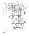
- FIG. 2shows an electrical schematic arrangement of a memory array employing the cell architecture illustrated in FIG. 1.
- the top portion of FIG. 2illustrates the transistors 207 and 211 coupled to the respective PCRAM memory elements 102 and 106 with the access transistors 207 and 211 coupling the memory elements 102 and 106 to the digit line 118 .
- a complementary digit line D 1 * 120is also provided in the memory array, to which another set of access transistors is connected which are in turn connected to other PCRAM memory elements.
- a single complementary pair of PCRAM cellsis illustrated as 300 . It includes transistor 207 and associated PCRAM memory element 102 , which is coupled to the digit line 118 (D 1 ), and an access transistor 209 and associated PCRAM memory element 124 , which are coupled to digit line 120 (D 1 *).
- a row line 104which is coupled to transistor 207 and a row line 113 which is coupled to transistor 209 are activated such that if PCRAM memory element 102 is written to a high resistance state, PCRAM element 124 is written to a low resistance state, and vice versa. In this way, PCRAM memory elements 102 and 124 are accessed together and always store complementary resistance digit values.
- a sense amplifier 210which is coupled to the digit lines 118 and 120 will read the value of PCRAM memory element 102 by comparing a discharging precharge voltage on digit line 118 to the discharging precharge voltage on digit line 120 during a memory read operation.
- a precharge voltageis applied to complementary digit lines 118 and 120 by a precharge circuit 301 .
- the precharge circuitis activated by a logic circuit on a precharge line which activates transistors 305 to supply a voltage, for example, Vcc/2, to both digit lines 118 and 120 .
- An equilibrate circuit 303may also be provided which is activated by an equilibrate signal after the precharge circuit is activated to ensure that the voltages on lines 118 and 120 are the same. The voltages on lines 118 and 120 are held by a parasitic capacitance of the lines.
- a read operationmay be conducted on the complimentary cell pair 300 . This read operation is illustrated in greater detail in FIG. 3, which is a simplification of the sense amplifier 210 input path.
- Parasitic capacitance for the complementary digit lines 118 and 120are illustrated as C 1 and C 1 *.
- the respective access transistors 207 and 209are illustrated as connected to their respective word lines 105 and 113 .
- the PCRAM memory elements 102 and 124are also illustrated.
- a binary valueis stored, for example, in memory PCRAM memory element 102 as a resistance value. It will be either a high resistance value or a low resistance value, and the complementary resistance value will be stored in PCRAM memory element 124 .
- the precharge voltage applied to the complementary digit lines 118 and 120is allowed to discharge through the access transistors 207 and 209 and through the respective resistance values of the PCRAM memory elements 102 and 124 . Because the resistance values will be different, one high and one low, the voltages on the digit lines D 1 and D * ( 118 , 120 ) will begin to diverge during a read operation.
- the voltage initially applied to the complementary digit lines 118 and 120is a voltage of Vcc/2, during a read operation this voltage actually is slightly higher by approximately 0.3 mV due to the presence of the parasitic capacitance C 1 and C* on the digit lines 118 and 120 , as well as gate-drain capacitance inherent within transistors 207 and 209 .
- FIG. 5illustrates the voltages on the complementary digit lines 118 and 120 during a read operation.
- the activation of the word lines 105 and 113is illustrated as a pulse signal, and initially the voltage of Vcc/2+approximately 0.3 mVwhich exists on both digit lines D 1 and D 1 * begins to decay.
- one PCRAM memory elemente.g. 102
- the voltage on the digit line associated with the lower resistance valuee.g. 124
- the divergence of the two voltages on the lines D 1 and D 1 *progressively increases.
- the sense amplifier 210is activated.
- the sense amplifiercan have an architecture typically employed in a DRAM arrangement which is illustrated in FIG. 4.
- Such a sense amplifierincludes an Nsense amplifier latch 302 and a Psense amplifier latch 304 . This structure is illustrated in FIG. 4.
- the N sense amplifieris fired first at a time t 1 .
- the digit line which has the lower voltage, e.g. D 1 * in the exampleis immediately pulled to ground.
- the Psense amplifieris fired at a time t 2 which drives the higher voltage line, e.g. D 1 , to Vcc.
- the sense amplifier 210outputs a value of Vcc indicating the high resistant state for the PCRAM memory element 102 .
- FIG. 5illustrates the signal timing which occurs when PCRAM memory element 102 has a higher resistance than memory element 104 , obviously the signal levels are reversed if PCRAM memory element 102 has a low resistance state and PCRAM memory element 124 has a high resistance state. That is, the signal diagrams illustrated in the FIG. 5 would have the digit line D 1 * going towards Vcc and the digit line D 1 going towards ground.
- FIG. 5also illustrates another aspect of the invention.
- the voltage for row lines 105 , 113increases from near ground level to a positive voltage near Vcc for a read operation. This voltage then returns to near ground level before the sense amplifier is enabled (before t 1 ). As a result, there is no rewriting of a read PCRAM memory element. If such rewriting of a PCRAM cell is desired, then the voltage on row line 105 , 113 having a memory element which is written to a low resistance state, may be at a voltage level near Vcc during operation of the sense amplifier 210 , which will automatically rewrite (refresh) the read cell to the low resistance state.
- programmable contact memory elementsare resistive rather than capacitive memory elements, it is possible they will take longer to pull the digit lines up to Vcc and to ground than a typical capacitive memory element found within a DRAM. Supposing that to be true, older DRAM sense amplifier designs that run somewhat slower than the latest generation of DRAM sense amplifiers could also be used with PCRAM memory cells. The advantage of doing so would be that these older DRAM sense amplifiers have already been shown to perform effectively, and their test infrastructure is already confirmed. Consequently, a hybrid memory consisting of PCRAM memory elements using DRAM sense amplifiers can be produced having the advantages of PCRAM technology, yet being producible quickly and inexpensively.
- FIG. 2shows the complementary programmable contact memory element 102 and 106 and associated access transistors and digit lines D and D* as being provided in the same memory array, the complementary memory elements, access transistors and digit lines may also be provided in respective different memory arrays.
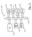
- FIG. 6is a block diagram of a processor-based system 400 utilizing a PCRAM memory device 200 constructed in accordance with one of the embodiments of the present invention.
- the processor-based system 400may be a computer system, a process control system or any other system employing a processor and associated memory.
- the system 400includes a central processing unit (CPU) 402 , e.g., a microprocessor, that communicates with the PCRAM memory device 408 and an I/O device 404 over a bus 420 .
- CPUcentral processing unit
- the bus 420may be a series of buses and bridges commonly used in a processor-based system, but for convenience purposes only, the bus 420 has been illustrated as a single bus.
- the processor-based system 400also includes read-only memory (ROM) 410 and may include peripheral devices such as a floppy disk drive 412 and a compact disk (CD) ROM drive 414 that also communicates with the CPU 402 over the bus 420 as is well known in the art.
- ROMread-only memory
- CDcompact disk
- One or more memory devices 200may be provided on a plug-in memory module 256 , e.g. SIMM, DIMM or other plug-in memory module, for easy connection with or disconnection from the bus 420 .
- a plug-in memory module 256e.g. SIMM, DIMM or other plug-in memory module, for easy connection with or disconnection from the bus 420 .
Landscapes
- Engineering & Computer Science (AREA)
- Computer Hardware Design (AREA)
- Dram (AREA)
- Semiconductor Memories (AREA)
- Measurement Of Resistance Or Impedance (AREA)
Abstract
Description
- The invention relates to a method and apparatus for sensing the resistance of a Programmable Conductor Random Access Memory (PCRAM) element.[0001]
- PCRAM devices store binary data as two different resistance values, one higher than the other. The resistance value represents a particular binary value of logic “0” or logic “1”. When sensing the resistance value of a PCRAM device, it is common to compare the resistance of a memory cell undergoing a read operation with resistance of a reference cell to determine the resistance value of the cell being read and thus its logic state. Such an approach is disclosed in U.S. Pat. No. 5,883,827. However, this approach has some limitations.[0002]
- If the reference cell is defective and a column of memory cells within an array uses a same defective reference cell, the entire column of memory cells will have erroneous resistance readings. In addition, specialized circuitry is required to write a resistance value into the reference cell, and a sense amplifier circuit for such an arrangement tends to be complex and large.[0003]
- Typically, sensing schemes for PCRAM devices also tend to have a unique architecture which is different from that normally employed in typical DRAM circuits. Although PCRAM's differ from DRAM's in that they store binary values in resistive memory elements rather than as charges on capacitors, and although PCRAM's are non-volatile, where the capacitor structures employed in DRAM's are volatile, nevertheless it would be desirable if the read and write circuits for both devices were as similar as possible so that existing DRAM memory device architectures could be easily adapted to read and write PCRAM devices.[0004]
- The present invention provides a PCRAM memory device and its method of operation which utilizes a read architecture similar to that employed in some DRAM memory devices. A pair of complementary PCRAM memory cells comprising first and second programmable conductor memory elements are employed, each connected to respective access transistors. During a write operation, the first and second memory elements are written with complementary binary values, that is: if the first memory element is written to a high resistance state, then the second memory element is written to a low resistance state; whereas if the first memory element is written to a low resistance state, the second memory element is written to a higher resistance state.[0005]
- During a read operation of, for example, the first memory element, a sense amplifier is connected so that its respective inputs are coupled to receive respective precharge voltages which discharge through the first and second memory elements. A sense amplifier reads the discharging voltages through the two memory elements to determine which is the larger voltage, thus determining the resistance (high or low) and logic state (high or low) of the memory cell being read.[0006]
- These and other features and advantages of the invention will become more apparent from the following detailed description of exemplary embodiments of the invention which are provided in connection with the accompanying drawings in which:[0007]
- FIG. 1 shows an exemplary PCRAM device;[0008]
- FIG. 2 is a schematic diagram depicting one aspect of the invention;[0009]
- FIG. 3 is a schematic diagram depicting an additional aspect of the invention;[0010]
- FIG. 4 is a schematic diagram depicting an additional aspect of the invention;[0011]
- FIG. 5 shows the discharge rate characteristics of capacitors employed in the invention;[0012]
- FIG. 6 shows the invention utilized in a computer system.[0013]
- The present invention employs a sense amplifier architecture which is somewhat similar to that employed in some conventional DRAM devices to sense the resistance states of PCRAM memory cells. In the invention, a binary value is stored as a resistance value in a first PCRAM cell while its complement resistance value is stored in a second PCRAM cell. During readout of the first PCRAM cell, both PCRAM cells are used to discharge a precharge voltage into respective inputs of a sense amplifier which reads the discharge voltages to determine the resistance and thus the binary value stored in the first PCRAM cell undergoing a read operation.[0014]
- FIG. 1 illustrates an exemplary cell arrangement provided within a portion of a PCRAM memory device constructed in accordance with the invention. A[0015]
PCRAM memory element 102 is illustrated which has a chalcogenite glass body and lower103 and upper104 conductors. As is well known, a programmable conductor memory element has two stable resistance states: one high resistance and one low resistance. Normally, when at rest the memory has a high resistance state, but it can be programmed to a low resistance state by suitably applying bias voltages to theconductors conductors - As further shown in FIG. 1, the[0016]
PCRAM memory element 102 is coupled by a conductive plug101 to anaccess transistor 207 which is driven by aword line 105 which forms the gate structure oftransistor 207. The access transistor is coupled through conductive plug101 to one of theconductors 103 of the PCRAM memory element. Theother conductor 104 of the PCRAM element is connected by acommon cell plate 109 to a bias voltage, which is common to other PCRAM memory elements provided in the memory device. - FIG. 1 illustrates a common PCRAM architecture in which two[0017]
adjacent memory cells common digit line 118. Thus, FIG. 1 also shows anotheraccess transistor 211 driven by aword line 107 which is connected throughconductive plug 99 to anotherPCRAM memory element 104, which in turn is also connected also to thecommon cell plate 109.Access transistor 211 also has one terminal connected todigit line 118. - FIG. 2 shows an electrical schematic arrangement of a memory array employing the cell architecture illustrated in FIG. 1. Thus, the top portion of FIG. 2 illustrates the[0018]
transistors PCRAM memory elements 102 and106 with theaccess transistors memory elements 102 and106 to thedigit line 118. - As also illustrated in FIG. 2, a complementary digit line D[0019]1*120 is also provided in the memory array, to which another set of access transistors is connected which are in turn connected to other PCRAM memory elements. To simplify discussion, a single complementary pair of PCRAM cells is illustrated as300. It includes
transistor 207 and associatedPCRAM memory element 102, which is coupled to the digit line118 (D1), and anaccess transistor 209 and associatedPCRAM memory element 124, which are coupled to digit line120 (D1*). - During a write operation, a[0020]
row line 104, which is coupled totransistor 207 and arow line 113 which is coupled totransistor 209 are activated such that ifPCRAM memory element 102 is written to a high resistance state,PCRAM element 124 is written to a low resistance state, and vice versa. In this way,PCRAM memory elements PCRAM memory element 102 is the primary element which is being written to and read from, asense amplifier 210 which is coupled to thedigit lines PCRAM memory element 102 by comparing a discharging precharge voltage ondigit line 118 to the discharging precharge voltage ondigit line 120 during a memory read operation. - Thus, prior to a memory read, a precharge voltage is applied to[0021]
complementary digit lines precharge circuit 301. The precharge circuit is activated by a logic circuit on a precharge line which activatestransistors 305 to supply a voltage, for example, Vcc/2, to bothdigit lines - An[0022]
equilibrate circuit 303 may also be provided which is activated by an equilibrate signal after the precharge circuit is activated to ensure that the voltages onlines lines complimentary cell pair 300. This read operation is illustrated in greater detail in FIG. 3, which is a simplification of thesense amplifier 210 input path. - Parasitic capacitance for the[0023]
complementary digit lines respective access transistors respective word lines PCRAM memory elements PCRAM memory element 102 as a resistance value. It will be either a high resistance value or a low resistance value, and the complementary resistance value will be stored inPCRAM memory element 124. - During a read operation, the precharge voltage applied to the[0024]
complementary digit lines access transistors PCRAM memory elements complementary digit lines digit lines transistors - FIG. 5 illustrates the voltages on the[0025]
complementary digit lines - The divergence of the two voltages on the lines D[0026]1 and D1* progressively increases. At a predetermined time after the word lines105 and113 are activated, the
sense amplifier 210 is activated. The sense amplifier can have an architecture typically employed in a DRAM arrangement which is illustrated in FIG. 4. Such a sense amplifier includes anNsense amplifier latch 302 and aPsense amplifier latch 304. This structure is illustrated in FIG. 4. - Reverting back to FIG. 5, the N sense amplifier is fired first at a time t[0027]1. When the Nsense amplifier fires, the digit line which has the lower voltage, e.g. D1* in the example, is immediately pulled to ground. Thereafter, the Psense amplifier is fired at a time t2which drives the higher voltage line, e.g. D1, to Vcc. Accordingly at a time t2, the
sense amplifier 210 outputs a value of Vcc indicating the high resistant state for thePCRAM memory element 102. - Although FIG. 5 illustrates the signal timing which occurs when[0028]
PCRAM memory element 102 has a higher resistance thanmemory element 104, obviously the signal levels are reversed ifPCRAM memory element 102 has a low resistance state andPCRAM memory element 124 has a high resistance state. That is, the signal diagrams illustrated in the FIG. 5 would have the digit line D1* going towards Vcc and the digit line D1 going towards ground. - FIG. 5 also illustrates another aspect of the invention. As shown, the voltage for[0029]
row lines row line sense amplifier 210, which will automatically rewrite (refresh) the read cell to the low resistance state. - Because programmable contact memory elements are resistive rather than capacitive memory elements, it is possible they will take longer to pull the digit lines up to Vcc and to ground than a typical capacitive memory element found within a DRAM. Supposing that to be true, older DRAM sense amplifier designs that run somewhat slower than the latest generation of DRAM sense amplifiers could also be used with PCRAM memory cells. The advantage of doing so would be that these older DRAM sense amplifiers have already been shown to perform effectively, and their test infrastructure is already confirmed. Consequently, a hybrid memory consisting of PCRAM memory elements using DRAM sense amplifiers can be produced having the advantages of PCRAM technology, yet being producible quickly and inexpensively.[0030]
- Although FIG. 2 shows the complementary programmable[0031]
contact memory element 102 and106 and associated access transistors and digit lines D and D* as being provided in the same memory array, the complementary memory elements, access transistors and digit lines may also be provided in respective different memory arrays. - FIG. 6 is a block diagram of a processor-based system[0032]400 utilizing a
PCRAM memory device 200 constructed in accordance with one of the embodiments of the present invention. The processor-based system400 may be a computer system, a process control system or any other system employing a processor and associated memory. The system400 includes a central processing unit (CPU)402, e.g., a microprocessor, that communicates with the PCRAM memory device408 and an I/O device 404 over abus 420. It must be noted that thebus 420 may be a series of buses and bridges commonly used in a processor-based system, but for convenience purposes only, thebus 420 has been illustrated as a single bus. A second I/O device406 is illustrated, but is not necessary to practice the invention. The processor-based system400 also includes read-only memory (ROM)410 and may include peripheral devices such as afloppy disk drive 412 and a compact disk (CD)ROM drive 414 that also communicates with the CPU402 over thebus 420 as is well known in the art. - One or[0033]
more memory devices 200 may be provided on a plug-inmemory module 256, e.g. SIMM, DIMM or other plug-in memory module, for easy connection with or disconnection from thebus 420. While the invention has been described and illustrated with reference to specific exemplary embodiments, it should be understood that many modifications and substitutions can be made without departing from the spirit and scope of the invention. Accordingly, the invention is not to be considered as limited by the foregoing description but is only limited by the scope of the appended claims.
Claims (58)
1. A PCRAM device, comprising:
a first and second digit line;
first and second programmable conductor memory elements for storing complementary binary digit values;
first and second access devices for respectively coupling said first and second conductor memory elements to said first and second digit lines; and
a sense amplifier having inputs respectively coupled to said first and second digit lines for reading a binary value stored as a resistance value in one of said memory elements.
2. A device as inclaim 1 further comprising a precharge circuit for precharging said digit lines to a common precharge voltage prior to a read operation.
3. A device as inclaim 1 further comprising a pair of row lines respectively coupled to said first and second access devices; and
circuitry for simultaneously activating said first and second row lines and therefore activating said first and second access devices.
4. A device as inclaim 3 wherein said first and second access devices are access transistors.
5. A device as inclaim 1 wherein said first and second programmable conductor memory elements are formed of a chalcogenite glass.
6. A device as inclaim 3 wherein when said access devices are activated, said precharge voltage on said digit lines discharges through a respective resistance of said first and second programmable conductor memory devices, said sense amplifier determining which of said memory devices has a high and low resistance state and outputting a binary value corresponding to the resistance state of said one memory element.
7. A device as inclaim 2 wherein said digit lines have an associated parasitic capacitance which stores said precharge voltage.
8. A device as inclaim 2 wherein said parasitic capacitance stores a voltage value which is larger than said precharge voltage.
9. A device as inclaim 3 wherein said row lines are activated in a manner which prevents an automatic refresh of at least one of said memory elements during a read operation.
10. A device as inclaim 3 wherein said row lines are activated in a manner which causes an automatic refresh of at least one of said memory elements during a read operation.
11. A device as inclaim 1 wherein said first and second memory elements are in a common memory array.
12. A device as inclaim 1 wherein said first and second memory elements are in different memory arrays.
13. A device as inclaim 2 further comprising an equiibrate circuit for equilibrating the voltage on said digit lines.
14. A memory device comprising:
a plurality of pairs of first and second programmable conductor random access memory cells, each pair of memory cells comprising:
first and second programmable conductor memory elements for storing complementary binary digit values;
first and second access devices for respectively coupling said first and second conductor memory elements to first and second digit lines; and
a sense amplifier having inputs respectively coupled to said first and second digit lines for reading a binary value stored as a resistance value in one of said memory elements.
15. A device as inclaim 14 further comprising a precharge circuit for precharging said digit lines to a common precharge voltage prior to a read operation.
16. A device as inclaim 14 further comprising a pair of row lines respectively coupled to said first and second access devices; and
circuitry for simultaneously activating said first and second row lines and therefore activating said first and second access devices.
17. A device as inclaim 16 wherein said first and second access devices are access transistors.
18. A device as inclaim 14 wherein said first and second programmable conductor memory elements are formed of a chalcogenite glass.
19. A device as inclaim 16 wherein when said access devices are activated, said precharge voltage on said digit lines discharges through a respective resistance of said first and second programmable conductor memory devices, said sense amplifier determining which of said memory devices has a high and low resistance state and outputting a binary value corresponding to the resistance state of said one memory element.
20. A device as inclaim 15 wherein said digit lines have an associated parasitic capacitance which stores said precharge voltage.
21. A device as inclaim 15 wherein said parasitic capacitance stores a voltage value which is larger than said precharge voltage.
22. A device as inclaim 16 wherein said row lines are activated in a manner which prevents an automatic refresh of at least one of said memory elements during a read operation.
23. A device as inclaim 16 wherein said row lines are activated in a manner which causes an automatic refresh of at least one of said memory elements during a read operation.
24. A device as inclaim 14 wherein said first and second memory elements are in a common memory array.
25. A device as inclaim 14 wherein said first and second memory elements are in different memory arrays.
26. A device as inclaim 15 further comprising an equilibrate circuit for equilibrating the precharge voltage on said digit lines.
27. A device as inclaim 14 wherein said memory device is provided on a memory module.
28. A device as inclaim 27 wherein said memory module is a plug-in memory module.
29. A computer system comprising:
a processor;
a memory system coupled to said processor, said memory system comprising:
a first and second digit line;
first and second programmable conductor memory elements for storing complementary binary digit values;
first and second access devices for respectively coupling said first and second conductor memory elements to said first and second digit lines; and
a sense amplifier having inputs respectively coupled to said first and second digit lines for reading a binary value stored as a resistance value in one of said memory elements.
30. A system as inclaim 29 further comprising a precharge circuit for precharging said digit lines to a common precharge voltage prior to a read operation.
31. A system as inclaim 29 further comprising a pair of row lines respectively coupled to said first and second access devices; and
circuitry for simultaneously activating said first and second row lines and therefore activating said first and second access devices.
32. A system as inclaim 31 wherein said first and second access devices are access transistors.
33. A system as inclaim 29 wherein said first and second programmable conductor memory elements are formed of a chalcogenite glass.
34. A system as inclaim 31 wherein when said access devices are activated, said precharge voltage on said digit lines discharges through a respective resistance of said first and second programmable conductor memory devices, said sense amplifier determining which of said memory devices has a high and low resistance state and outputting a binary value corresponding to the resistance state of said one memory element.
35. A system as inclaim 30 wherein said digit lines have an associated parasitic capacitance which stores said precharge voltage.
36. A system as inclaim 30 wherein said parasitic capacitance stores a voltage value which is larger than said precharge voltage.
37. A system as inclaim 31 wherein said row lines are activated in a manner which prevents an automatic refresh of at least one of said memory elements during a read operation.
38. A system as inclaim 31 wherein said row lines are activated in a manner which causes an automatic refresh of at least one of said memory elements during a read operation.
39. A system as inclaim 29 wherein said first and second memory elements are in a common memory array.
40. A system as inclaim 29 wherein said first and second memory elements are in different memory arrays.
41. A system as inclaim 30 further comprising an equilibrate circuit for equilibrating the voltage on said digit lines.
42. A method of operating a programmable conductor memory device comprising:
storing a binary value as respective different resistance states in a first and second programmable conductor memory element;
determining a binary value stored in one of said memory elements by discharging respective voltages through said memory elements and comparing the discharging voltages.
43. A method as inclaim 42 wherein said discharging comprises:
precharging complementary digit lines to a voltage value; and
discharging the voltage value on each of said complementary digit lines through a respective memory element.
44. A method as inclaim 43 wherein said precharged voltage value on said complementary digit lines is discharged through said respective memory elements by enabling access transistors respectively associated with each of said memory elements.
45. A method as nclaim 44 further comprising completing said precharge before enabling said access transistors.
46. A method as inclaim 45 further comprising equilibrating said digit lines before enabling said access transistors.
47. A method as inclaim 44 where said comparison comprises:
determining whether the discharging voltage associated with one memory element is the higher or lower of the two discharging voltages and outputting a first binary value if the discharging voltage associated with the said one memory element is the higher voltage and outputting a second binary value if the discharging voltage associated with said one memory element is the lower voltage.
48. A method as inclaim 47 further comprising setting a digit line having a higher discharge voltage to a first predetermined voltage state and setting a digit line having a lower discharging voltage to a second predetermined voltage state.
49. A method as inclaim 48 wherein said first predetermined voltage is higher than said second predetermined voltage.
50. A method as inclaim 49 wherein said second predetermined voltage is ground voltage.
51. A method as inclaim 48 further comprising disabling said access transistors before said digit lines are set to said first and second voltage states.
52. A method as inclaim 48 further comprising enabling at least one of said access transistors during a time when said digit lines are set to said first and second voltage states.
53. A method of producing a programmable conductor memory device, said method comprising;
forming first and second digit lines;
forming first and second programmable conductor memory elements;
forming first and second access transistors for respectively coupling said first and second memory elements to said first and second digit lines;
forming a precharge circuit for precharging said first and second digit lines to a first voltage;
forming respective row lines for operating said access transistors to couple said memory elements to respective digit lines; and
forming a sense amplifier which has inputs respectively coupled to said digit lines.
54. A method as inclaim 53 further comprising forming a row decoder for decoding row address signals and selectively and simultaneously enabling said word lines.
55. A method as inclaim 53 wherein said memory elements are formed of a chalcogenite glass.
56. A method as inclaim 53 wherein said memory elements are fabricated in a common memory array.
57. A method as inclaim 53 wherein said memory elements are fabricated in different memory arrays.
58. A method as inclaim 53 further comprising forming an equilibrate circuit for equilibrating said digit lines.
Priority Applications (13)
| Application Number | Priority Date | Filing Date | Title |
|---|---|---|---|
| US09/988,627US6791859B2 (en) | 2001-11-20 | 2001-11-20 | Complementary bit PCRAM sense amplifier and method of operation |
| CNB028273702ACN100483549C (en) | 2001-11-20 | 2002-11-20 | Resistive memory device, method of operating and forming the same, and computer system including the same |
| JP2003546353AJP4681809B2 (en) | 2001-11-20 | 2002-11-20 | Complementary bit PCRAM sense amplifier and method of operation thereof |
| KR1020047007723AKR100794878B1 (en) | 2001-11-20 | 2002-11-20 | Complementary Bits PCRAM (Programmable Conductor RAM) and Operation Method |
| KR1020087009769AKR100918171B1 (en) | 2001-11-20 | 2002-11-20 | Method of producing and forming a memory device |
| KR1020077016929AKR20070087208A (en) | 2001-11-20 | 2002-11-20 | How to create and form a memory device |
| PCT/US2002/037227WO2003044802A2 (en) | 2001-11-20 | 2002-11-20 | Complementary bit pcram (programmable conductor ram) and method of operation |
| AU2002352816AAU2002352816A1 (en) | 2001-11-20 | 2002-11-20 | Complementary bit pcram (programmable conductor ram) and method of operation |
| EP02789771AEP1454325A2 (en) | 2001-11-20 | 2002-11-20 | Complementary bit pcram sense amplifier and method of operation |
| US10/866,091US7002833B2 (en) | 2001-11-20 | 2004-06-14 | Complementary bit resistance memory sensor and method of operation |
| US11/236,562US7242603B2 (en) | 2001-11-20 | 2005-09-28 | Method of operating a complementary bit resistance memory sensor |
| US11/476,043US7366003B2 (en) | 2001-11-20 | 2006-06-28 | Method of operating a complementary bit resistance memory sensor and method of operation |
| US12/073,901US7869249B2 (en) | 2001-11-20 | 2008-03-11 | Complementary bit PCRAM sense amplifier and method of operation |
Applications Claiming Priority (1)
| Application Number | Priority Date | Filing Date | Title |
|---|---|---|---|
| US09/988,627US6791859B2 (en) | 2001-11-20 | 2001-11-20 | Complementary bit PCRAM sense amplifier and method of operation |
Related Child Applications (1)
| Application Number | Title | Priority Date | Filing Date |
|---|---|---|---|
| US10/866,091ContinuationUS7002833B2 (en) | 2001-11-20 | 2004-06-14 | Complementary bit resistance memory sensor and method of operation |
Publications (2)
| Publication Number | Publication Date |
|---|---|
| US20030095426A1true US20030095426A1 (en) | 2003-05-22 |
| US6791859B2 US6791859B2 (en) | 2004-09-14 |
Family
ID=25534332
Family Applications (5)
| Application Number | Title | Priority Date | Filing Date |
|---|---|---|---|
| US09/988,627Expired - LifetimeUS6791859B2 (en) | 2001-11-20 | 2001-11-20 | Complementary bit PCRAM sense amplifier and method of operation |
| US10/866,091Expired - Fee RelatedUS7002833B2 (en) | 2001-11-20 | 2004-06-14 | Complementary bit resistance memory sensor and method of operation |
| US11/236,562Expired - Fee RelatedUS7242603B2 (en) | 2001-11-20 | 2005-09-28 | Method of operating a complementary bit resistance memory sensor |
| US11/476,043Expired - LifetimeUS7366003B2 (en) | 2001-11-20 | 2006-06-28 | Method of operating a complementary bit resistance memory sensor and method of operation |
| US12/073,901Expired - Fee RelatedUS7869249B2 (en) | 2001-11-20 | 2008-03-11 | Complementary bit PCRAM sense amplifier and method of operation |
Family Applications After (4)
| Application Number | Title | Priority Date | Filing Date |
|---|---|---|---|
| US10/866,091Expired - Fee RelatedUS7002833B2 (en) | 2001-11-20 | 2004-06-14 | Complementary bit resistance memory sensor and method of operation |
| US11/236,562Expired - Fee RelatedUS7242603B2 (en) | 2001-11-20 | 2005-09-28 | Method of operating a complementary bit resistance memory sensor |
| US11/476,043Expired - LifetimeUS7366003B2 (en) | 2001-11-20 | 2006-06-28 | Method of operating a complementary bit resistance memory sensor and method of operation |
| US12/073,901Expired - Fee RelatedUS7869249B2 (en) | 2001-11-20 | 2008-03-11 | Complementary bit PCRAM sense amplifier and method of operation |
Country Status (7)
| Country | Link |
|---|---|
| US (5) | US6791859B2 (en) |
| EP (1) | EP1454325A2 (en) |
| JP (1) | JP4681809B2 (en) |
| KR (3) | KR100918171B1 (en) |
| CN (1) | CN100483549C (en) |
| AU (1) | AU2002352816A1 (en) |
| WO (1) | WO2003044802A2 (en) |
Cited By (150)
| Publication number | Priority date | Publication date | Assignee | Title |
|---|---|---|---|---|
| US20020116955A1 (en)* | 2001-02-19 | 2002-08-29 | Sumitomo Electric Industries, Ltd. | Method of forming soot preform |
| US20020168852A1 (en)* | 2001-05-11 | 2002-11-14 | Harshfield Steven T. | PCRAM memory cell and method of making same |
| US20030027416A1 (en)* | 2001-08-01 | 2003-02-06 | Moore John T. | Method of forming integrated circuitry, method of forming memory circuitry, and method of forming random access memory circuitry |
| US20030045054A1 (en)* | 2001-08-29 | 2003-03-06 | Campbell Kristy A. | Method of forming non-volatile resistance variable devices, method of forming a programmable memory cell of memory circuitry, and a non-volatile resistance variable device |
| US20030045049A1 (en)* | 2001-08-29 | 2003-03-06 | Campbell Kristy A. | Method of forming chalcogenide comprising devices |
| US20030047772A1 (en)* | 2001-03-15 | 2003-03-13 | Jiutao Li | Agglomeration elimination for metal sputter deposition of chalcogenides |
| US20030156463A1 (en)* | 2002-02-19 | 2003-08-21 | Casper Stephen L. | Programmable conductor random access memory and method for sensing same |
| US20030169625A1 (en)* | 2002-03-05 | 2003-09-11 | Glen Hush | Programmable conductor random access memory and method for sensing same |
| US20030173558A1 (en)* | 2002-03-14 | 2003-09-18 | Campbell Kristy A. | Methods and apparatus for resistance variable material cells |
| US20030194865A1 (en)* | 2002-04-10 | 2003-10-16 | Gilton Terry L. | Method of manufacture of programmable conductor memory |
| US20030193053A1 (en)* | 2002-04-10 | 2003-10-16 | Gilton Terry L. | Thin film diode integrated with chalcogenide memory cell |
| US20030193059A1 (en)* | 2002-04-10 | 2003-10-16 | Gilton Terry L. | Programmable conductor memory cell structure and method therefor |
| US20030206433A1 (en)* | 2002-05-03 | 2003-11-06 | Glen Hush | Dual write cycle programmable conductor memory system and method of operation |
| US20030228717A1 (en)* | 2002-06-06 | 2003-12-11 | Jiutao Li | Co-sputter deposition of metal-doped chalcogenides |
| US20040032782A1 (en)* | 2001-10-24 | 2004-02-19 | Glen Hush | System and method for power saving memory refresh for dynamic random access memory devices after an extended interval |
| US20040038480A1 (en)* | 2002-08-22 | 2004-02-26 | Moore John T. | Method of manufacture of a PCRAM memory cell |
| US20040040835A1 (en)* | 2002-08-29 | 2004-03-04 | Jiutao Li | Silver selenide film stoichiometry and morphology control in sputter deposition |
| US20040043553A1 (en)* | 2002-06-06 | 2004-03-04 | Jiutao Li | Elimination of dendrite formation during metal/chalcogenide glass deposition |
| US20040071042A1 (en)* | 2002-01-04 | 2004-04-15 | John Moore | PCRAM rewrite prevention |
| US20040157417A1 (en)* | 2002-08-29 | 2004-08-12 | Moore John T. | Methods to form a memory cell with metal-rich metal chalcogenide |
| US6791859B2 (en) | 2001-11-20 | 2004-09-14 | Micron Technology, Inc. | Complementary bit PCRAM sense amplifier and method of operation |
| US20040180533A1 (en)* | 2003-03-14 | 2004-09-16 | Li Li | Method for filling via with metal |
| US20040192006A1 (en)* | 2002-02-20 | 2004-09-30 | Campbell Kristy A. | Layered resistance variable memory device and method of fabrication |
| US6813176B2 (en) | 2001-08-30 | 2004-11-02 | Micron Technology, Inc. | Method of retaining memory state in a programmable conductor RAM |
| US20040223390A1 (en)* | 2002-02-15 | 2004-11-11 | Campbell Kristy A. | Resistance variable memory element having chalcogenide glass for improved switching characteristics |
| US20040223357A1 (en)* | 2002-02-20 | 2004-11-11 | Gilton Terry L. | Multiple data state memory cell |
| US20040229423A1 (en)* | 2001-11-19 | 2004-11-18 | Moore John T. | Electrode structure for use in an integrated circuit |
| US6847535B2 (en) | 2002-02-20 | 2005-01-25 | Micron Technology, Inc. | Removable programmable conductor memory card and associated read/write device and method of operation |
| US20050017233A1 (en)* | 2003-07-21 | 2005-01-27 | Campbell Kristy A. | Performance PCRAM cell |
| US20050026433A1 (en)* | 2001-08-30 | 2005-02-03 | Jiutao Li | Integrated circuit device and fabrication using metal-doped chalcogenide materials |
| US20050054207A1 (en)* | 2002-08-29 | 2005-03-10 | Micron Technology, Inc. | Plasma etching methods and methods of forming memory devices comprising a chalcogenide comprising layer received operably proximate conductive electrodes |
| US20050056910A1 (en)* | 2003-09-17 | 2005-03-17 | Gilton Terry L. | Non-volatile memory structure |
| US20050162883A1 (en)* | 2002-08-08 | 2005-07-28 | Hasan Nejad | Columnar 1T-nMemory cell structure and its method of formation and operation |
| US6930909B2 (en) | 2003-06-25 | 2005-08-16 | Micron Technology, Inc. | Memory device and methods of controlling resistance variation and resistance profile drift |
| US20050202588A1 (en)* | 2004-03-10 | 2005-09-15 | Brooks Joseph F. | Method of forming a chalcogenide material containing device |
| US20050201174A1 (en)* | 2004-03-10 | 2005-09-15 | Klein Dean A. | Power management control and controlling memory refresh operations |
| US6961277B2 (en) | 2003-07-08 | 2005-11-01 | Micron Technology, Inc. | Method of refreshing a PCRAM memory device |
| US20060012008A1 (en)* | 2004-07-19 | 2006-01-19 | Campbell Kristy A | Resistance variable memory device and method of fabrication |
| US20060011910A1 (en)* | 2004-07-19 | 2006-01-19 | Micron Technology, Inc. | PCRAM device with switching glass layer |
| US20060035403A1 (en)* | 2004-08-12 | 2006-02-16 | Campbell Kristy A | PCRAM device with switching glass layer |
| US20060033094A1 (en)* | 2004-08-12 | 2006-02-16 | Campbell Kristy A | Resistance variable memory with temperature tolerant materials |
| US20060044906A1 (en)* | 2004-09-01 | 2006-03-02 | Ethan Williford | Sensing of resistance variable memory devices |
| US7010644B2 (en) | 2002-08-29 | 2006-03-07 | Micron Technology, Inc. | Software refreshed memory device and method |
| US20060131555A1 (en)* | 2004-12-22 | 2006-06-22 | Micron Technology, Inc. | Resistance variable devices with controllable channels |
| US20060131556A1 (en)* | 2004-12-22 | 2006-06-22 | Micron Technology, Inc. | Small electrode for resistance variable devices |
| US20060237707A1 (en)* | 2005-04-22 | 2006-10-26 | Micron Technology, Inc. | Memory array for increased bit density and method of forming the same |
| US20060252176A1 (en)* | 2002-08-29 | 2006-11-09 | Micron Technology, Inc. | Memory element and its method of formation |
| US20060256640A1 (en)* | 2005-05-16 | 2006-11-16 | Micron Technology, Inc. | Power circuits for reducing a number of power supply voltage taps required for sensing a resistive memory |
| US20060270099A1 (en)* | 2001-08-29 | 2006-11-30 | Micron Technology, Inc. | Method of forming non-volatile resistance variable devices and method of forming a programmable memory cell of memory circuitry |
| US20070008768A1 (en)* | 2005-07-08 | 2007-01-11 | Micron Technology, Inc. | Process for erasing chalcogenide variable resistance memory bits |
| US20070007506A1 (en)* | 2002-02-20 | 2007-01-11 | Micron Technology, Inc. | Layered resistance variable memory device and method of fabrication |
| US7163837B2 (en) | 2002-08-29 | 2007-01-16 | Micron Technology, Inc. | Method of forming a resistance variable memory element |
| US20070023744A1 (en)* | 2005-08-01 | 2007-02-01 | Micron Technology, Inc. | Resistance variable memory device with sputtered metal-chalcogenide region and method of fabrication |
| US20070030554A1 (en)* | 2005-08-02 | 2007-02-08 | Micron Technology, Inc. | Method and apparatus for providing color changing thin film material |
| US20070037316A1 (en)* | 2005-08-09 | 2007-02-15 | Micron Technology, Inc. | Memory cell contact using spacers |
| US20070034921A1 (en)* | 2005-08-09 | 2007-02-15 | Micron Technology, Inc. | Access transistor for memory device |
| US20070035990A1 (en)* | 2005-08-15 | 2007-02-15 | Micron Technology, Inc. | Method and apparatus providing a cross-point memory array using a variable resistance memory cell and capacitance |
| US20070047297A1 (en)* | 2005-08-31 | 2007-03-01 | Campbell Kristy A | Resistance variable memory element with threshold device and method of forming the same |
| US20070059882A1 (en)* | 2005-04-22 | 2007-03-15 | Micron Technology, Inc. | Memory elements having patterned electrodes and method of forming the same |
| US20070090354A1 (en)* | 2005-08-11 | 2007-04-26 | Micron Technology, Inc. | Chalcogenide-based electrokinetic memory element and method of forming the same |
| US20070108431A1 (en)* | 2005-11-15 | 2007-05-17 | Chen Shih H | I-shaped phase change memory cell |
| US20070147105A1 (en)* | 2005-11-28 | 2007-06-28 | Macronix International Co., Ltd. | Phase Change Memory Cell and Manufacturing Method |
| US7269044B2 (en) | 2005-04-22 | 2007-09-11 | Micron Technology, Inc. | Method and apparatus for accessing a memory array |
| US7294527B2 (en) | 2002-08-29 | 2007-11-13 | Micron Technology Inc. | Method of forming a memory cell |
| US7317200B2 (en) | 2005-02-23 | 2008-01-08 | Micron Technology, Inc. | SnSe-based limited reprogrammable cell |
| US7332735B2 (en) | 2005-08-02 | 2008-02-19 | Micron Technology, Inc. | Phase change memory cell and method of formation |
| US20080043520A1 (en)* | 2006-02-07 | 2008-02-21 | Chen Shih H | I-shaped phase change memory cell with thermal isolation |
| US20080185730A1 (en)* | 2007-02-02 | 2008-08-07 | Macronix International Co., Ltd. | Memory cell device with coplanar electrode surface and method |
| US20080191186A1 (en)* | 2007-02-14 | 2008-08-14 | Macronix International Co., Ltd. | Phase change memory cell with filled sidewall memory element and method for fabricating the same |
| US20080258126A1 (en)* | 2007-04-17 | 2008-10-23 | Macronix International Co., Ltd. | Memory Cell Sidewall Contacting Side Electrode |
| US7459717B2 (en) | 2005-11-28 | 2008-12-02 | Macronix International Co., Ltd. | Phase change memory cell and manufacturing method |
| US7476587B2 (en) | 2006-12-06 | 2009-01-13 | Macronix International Co., Ltd. | Method for making a self-converged memory material element for memory cell |
| US20090020740A1 (en)* | 2007-07-20 | 2009-01-22 | Macronix International Co., Ltd. | Resistive memory structure with buffer layer |
| US20090101879A1 (en)* | 2007-10-22 | 2009-04-23 | Macronix International Co., Ltd. | Method for Making Self Aligning Pillar Memory Cell Device |
| US20090148981A1 (en)* | 2005-12-27 | 2009-06-11 | Macronix International Co., Ltd. | Method for forming self-aligned thermal isolation cell for a variable resistance memory array |
| US20090147564A1 (en)* | 2007-12-07 | 2009-06-11 | Macronix International Co., Ltd. | Phase change memory cell having interface structures with essentially equal thermal impedances and manufacturing methods |
| US7560337B2 (en) | 2006-01-09 | 2009-07-14 | Macronix International Co., Ltd. | Programmable resistive RAM and manufacturing method |
| US20090189138A1 (en)* | 2008-01-28 | 2009-07-30 | Macronix International Co., Ltd. | Fill-in etching free pore device |
| US20090242880A1 (en)* | 2008-03-25 | 2009-10-01 | Macronix International Co., Ltd. | Thermally stabilized electrode structure |
| US20090242865A1 (en)* | 2008-03-31 | 2009-10-01 | Macronix International Co., Ltd | Memory array with diode driver and method for fabricating the same |
| US7599217B2 (en) | 2005-11-22 | 2009-10-06 | Macronix International Co., Ltd. | Memory cell device and manufacturing method |
| US20090251944A1 (en)* | 2008-04-07 | 2009-10-08 | Macronix International Co., Ltd. | Memory cell having improved mechanical stability |
| US20090261313A1 (en)* | 2008-04-22 | 2009-10-22 | Macronix International Co., Ltd. | Memory cell having a buried phase change region and method for fabricating the same |
| US20090261316A1 (en)* | 2006-08-29 | 2009-10-22 | Jun Liu | Enhanced memory density resistance variable memory cells, arrays, devices and systems including the same, and methods of fabrication |
| US20090279349A1 (en)* | 2008-05-08 | 2009-11-12 | Macronix International Co., Ltd. | Phase change device having two or more substantial amorphous regions in high resistance state |
| US20090309087A1 (en)* | 2008-06-12 | 2009-12-17 | Macronix International Co., Ltd. | Phase change memory cell having top and bottom sidewall contacts |
| US7639527B2 (en) | 2008-01-07 | 2009-12-29 | Macronix International Co., Ltd. | Phase change memory dynamic resistance test and manufacturing methods |
| US7642123B2 (en) | 2005-11-15 | 2010-01-05 | Macronix International Co., Ltd. | Thermally insulated phase change memory manufacturing method |
| US20100019215A1 (en)* | 2008-07-22 | 2010-01-28 | Macronix International Co., Ltd. | Mushroom type memory cell having self-aligned bottom electrode and diode access device |
| US20100046285A1 (en)* | 2008-08-19 | 2010-02-25 | Macronix International Co., Ltd. | Multiple phase change materials in an integrated circuit for system on a chip application |
| US20100067289A1 (en)* | 2008-09-12 | 2010-03-18 | Elpida Menory, Inc. | Semiconductor device |
| US20100067285A1 (en)* | 2008-09-12 | 2010-03-18 | Macronix International Co., Ltd. | Novel sensing circuit for pcram applications |
| US20100084624A1 (en)* | 2008-10-02 | 2010-04-08 | Macronix International Co., Ltd. | Dielectric mesh isolated phase change structure for phase change memory |
| US20100110778A1 (en)* | 2008-11-06 | 2010-05-06 | Macronix International Co., Ltd. | Phase change memory program method without over-reset |
| US20100117048A1 (en)* | 2008-11-07 | 2010-05-13 | Macronix International Co., Ltd. | Memory cell access device having a pn-junction with polycrystalline and single-crystal semiconductor regions |
| US20100117049A1 (en)* | 2008-11-07 | 2010-05-13 | Macronix International Co., Ltd. | Memory cell access device having a pn-junction with polycrystalline plug and single-crystal semiconductor regions |
| US7741636B2 (en) | 2006-01-09 | 2010-06-22 | Macronix International Co., Ltd. | Programmable resistive RAM and manufacturing method |
| US7742330B2 (en) | 2004-05-25 | 2010-06-22 | Renesas Technology Corp. | Semiconductor device |
| US20100171086A1 (en)* | 2009-01-07 | 2010-07-08 | Macronix International Co., Ltd. | Integrated circuit memory with single crystal silicon on silicide driver and manufacturing method |
| US20100181649A1 (en)* | 2009-01-22 | 2010-07-22 | Macronix International Co., Ltd. | Polysilicon pillar bipolar transistor with self-aligned memory element |
| US7786461B2 (en) | 2007-04-03 | 2010-08-31 | Macronix International Co., Ltd. | Memory structure with reduced-size memory element between memory material portions |
| US7786460B2 (en) | 2005-11-15 | 2010-08-31 | Macronix International Co., Ltd. | Phase change memory device and manufacturing method |
| US7785920B2 (en) | 2006-07-12 | 2010-08-31 | Macronix International Co., Ltd. | Method for making a pillar-type phase change memory element |
| US20100264396A1 (en)* | 2009-04-20 | 2010-10-21 | Macronix International Co., Ltd. | Ring-shaped electrode and manufacturing method for same |
| US20100295009A1 (en)* | 2009-05-22 | 2010-11-25 | Macronix International Co., Ltd. | Phase Change Memory Cells Having Vertical Channel Access Transistor and Memory Plane |
| US7863655B2 (en) | 2006-10-24 | 2011-01-04 | Macronix International Co., Ltd. | Phase change memory cells with dual access devices |
| US7869270B2 (en) | 2008-12-29 | 2011-01-11 | Macronix International Co., Ltd. | Set algorithm for phase change memory cell |
| US7867815B2 (en) | 2005-11-16 | 2011-01-11 | Macronix International Co., Ltd. | Spacer electrode small pin phase change RAM and manufacturing method |
| US20110037558A1 (en)* | 2008-08-01 | 2011-02-17 | Boise State University | Continuously variable resistor |
| US7894254B2 (en) | 2009-07-15 | 2011-02-22 | Macronix International Co., Ltd. | Refresh circuitry for phase change memory |
| US7897954B2 (en) | 2008-10-10 | 2011-03-01 | Macronix International Co., Ltd. | Dielectric-sandwiched pillar memory device |
| US7903447B2 (en) | 2006-12-13 | 2011-03-08 | Macronix International Co., Ltd. | Method, apparatus and computer program product for read before programming process on programmable resistive memory cell |
| US7910906B2 (en) | 2006-10-04 | 2011-03-22 | Macronix International Co., Ltd. | Memory cell device with circumferentially-extending memory element |
| US7932506B2 (en) | 2008-07-22 | 2011-04-26 | Macronix International Co., Ltd. | Fully self-aligned pore-type memory cell having diode access device |
| US7933139B2 (en) | 2009-05-15 | 2011-04-26 | Macronix International Co., Ltd. | One-transistor, one-resistor, one-capacitor phase change memory |
| US7956344B2 (en) | 2007-02-27 | 2011-06-07 | Macronix International Co., Ltd. | Memory cell with memory element contacting ring-shaped upper end of bottom electrode |
| US7968876B2 (en) | 2009-05-22 | 2011-06-28 | Macronix International Co., Ltd. | Phase change memory cell having vertical channel access transistor |
| US7978509B2 (en) | 2007-08-02 | 2011-07-12 | Macronix International Co., Ltd. | Phase change memory with dual word lines and source lines and method of operating same |
| US8030635B2 (en) | 2009-01-13 | 2011-10-04 | Macronix International Co., Ltd. | Polysilicon plug bipolar transistor for phase change memory |
| US8062833B2 (en) | 2005-12-30 | 2011-11-22 | Macronix International Co., Ltd. | Chalcogenide layer etching method |
| US8064247B2 (en) | 2009-01-14 | 2011-11-22 | Macronix International Co., Ltd. | Rewritable memory device based on segregation/re-absorption |
| US8064248B2 (en) | 2009-09-17 | 2011-11-22 | Macronix International Co., Ltd. | 2T2R-1T1R mix mode phase change memory array |
| US8077505B2 (en) | 2008-05-07 | 2011-12-13 | Macronix International Co., Ltd. | Bipolar switching of phase change device |
| US8097871B2 (en) | 2009-04-30 | 2012-01-17 | Macronix International Co., Ltd. | Low operational current phase change memory structures |
| US8107283B2 (en) | 2009-01-12 | 2012-01-31 | Macronix International Co., Ltd. | Method for setting PCRAM devices |
| US8110822B2 (en) | 2009-07-15 | 2012-02-07 | Macronix International Co., Ltd. | Thermal protect PCRAM structure and methods for making |
| US8110430B2 (en) | 2005-11-21 | 2012-02-07 | Macronix International Co., Ltd. | Vacuum jacket for phase change memory element |
| JP2012039134A (en)* | 2004-05-14 | 2012-02-23 | Renesas Electronics Corp | Semiconductor integrated circuit device manufacturing method |
| US8134857B2 (en) | 2008-06-27 | 2012-03-13 | Macronix International Co., Ltd. | Methods for high speed reading operation of phase change memory and device employing same |
| US8158965B2 (en) | 2008-02-05 | 2012-04-17 | Macronix International Co., Ltd. | Heating center PCRAM structure and methods for making |
| US8173987B2 (en) | 2009-04-27 | 2012-05-08 | Macronix International Co., Ltd. | Integrated circuit 3D phase change memory array and manufacturing method |
| US8178387B2 (en) | 2009-10-23 | 2012-05-15 | Macronix International Co., Ltd. | Methods for reducing recrystallization time for a phase change material |
| US8178405B2 (en) | 2006-12-28 | 2012-05-15 | Macronix International Co., Ltd. | Resistor random access memory cell device |
| US8198619B2 (en) | 2009-07-15 | 2012-06-12 | Macronix International Co., Ltd. | Phase change memory cell structure |
| US8238149B2 (en) | 2009-06-25 | 2012-08-07 | Macronix International Co., Ltd. | Methods and apparatus for reducing defect bits in phase change memory |
| US8310864B2 (en) | 2010-06-15 | 2012-11-13 | Macronix International Co., Ltd. | Self-aligned bit line under word line memory array |
| US8363463B2 (en) | 2009-06-25 | 2013-01-29 | Macronix International Co., Ltd. | Phase change memory having one or more non-constant doping profiles |
| US8395935B2 (en) | 2010-10-06 | 2013-03-12 | Macronix International Co., Ltd. | Cross-point self-aligned reduced cell size phase change memory |
| US8406033B2 (en) | 2009-06-22 | 2013-03-26 | Macronix International Co., Ltd. | Memory device and method for sensing and fixing margin cells |
| US8467238B2 (en) | 2010-11-15 | 2013-06-18 | Macronix International Co., Ltd. | Dynamic pulse operation for phase change memory |
| US8497705B2 (en) | 2010-11-09 | 2013-07-30 | Macronix International Co., Ltd. | Phase change device for interconnection of programmable logic device |
| US8729521B2 (en) | 2010-05-12 | 2014-05-20 | Macronix International Co., Ltd. | Self aligned fin-type programmable memory cell |
| US20140169069A1 (en)* | 2012-12-18 | 2014-06-19 | Hyung-Rok Oh | Resistive Memory Device, System Including the Same and Method of Reading Data in the Same |
| US8809829B2 (en) | 2009-06-15 | 2014-08-19 | Macronix International Co., Ltd. | Phase change memory having stabilized microstructure and manufacturing method |
| US8987700B2 (en) | 2011-12-02 | 2015-03-24 | Macronix International Co., Ltd. | Thermally confined electrode for programmable resistance memory |
| US9336879B2 (en) | 2014-01-24 | 2016-05-10 | Macronix International Co., Ltd. | Multiple phase change materials in an integrated circuit for system on a chip application |
| US9559113B2 (en) | 2014-05-01 | 2017-01-31 | Macronix International Co., Ltd. | SSL/GSL gate oxide in 3D vertical channel NAND |
| US9672906B2 (en) | 2015-06-19 | 2017-06-06 | Macronix International Co., Ltd. | Phase change memory with inter-granular switching |
| CN112204663A (en)* | 2018-05-31 | 2021-01-08 | 美光科技公司 | Sensing operations in memory |
| US20220261624A1 (en)* | 2017-11-29 | 2022-08-18 | Anaflash Inc. | Neural network circuits having non-volatile synapse arrays |
Families Citing this family (75)
| Publication number | Priority date | Publication date | Assignee | Title |
|---|---|---|---|---|
| JP4218527B2 (en)* | 2002-02-01 | 2009-02-04 | 株式会社日立製作所 | Storage device |
| US7800932B2 (en)* | 2005-09-28 | 2010-09-21 | Sandisk 3D Llc | Memory cell comprising switchable semiconductor memory element with trimmable resistance |
| US20060203541A1 (en) | 2003-03-18 | 2006-09-14 | Haruki Toda | Phase change memory device |
| KR100504700B1 (en)* | 2003-06-04 | 2005-08-03 | 삼성전자주식회사 | Phase random access memory with high dencity |
| US6987688B2 (en)* | 2003-06-11 | 2006-01-17 | Ovonyx, Inc. | Die customization using programmable resistance memory elements |
| JP4356542B2 (en)* | 2003-08-27 | 2009-11-04 | 日本電気株式会社 | Semiconductor device |
| US7123530B2 (en)* | 2003-10-09 | 2006-10-17 | Micron Technology, Inc. | AC sensing for a resistive memory |
| TW200527656A (en)* | 2004-02-05 | 2005-08-16 | Renesas Tech Corp | Semiconductor device |
| KR100733147B1 (en)* | 2004-02-25 | 2007-06-27 | 삼성전자주식회사 | Phase change memory device and manufacturing method thereof |
| US7145795B2 (en)* | 2004-04-13 | 2006-12-05 | Micron Technology, Inc. | Multi-cell resistive memory array architecture with select transistor |
| WO2005106955A1 (en)* | 2004-04-27 | 2005-11-10 | Matsushita Electric Industrial Co., Ltd. | Storage element |
| KR100567067B1 (en)* | 2004-06-30 | 2006-04-04 | 주식회사 하이닉스반도체 | Phase change memory device and manufacturing method thereof |
| KR100610008B1 (en)* | 2004-07-19 | 2006-08-08 | 삼성전자주식회사 | Phase change memory device suitable for burst read operation and data reading method accordingly |
| DE102004045219B4 (en)* | 2004-09-17 | 2011-07-28 | Qimonda AG, 81739 | Arrangement and method for reading resistance memory cells |
| US7423897B2 (en)* | 2004-10-01 | 2008-09-09 | Ovonyx, Inc. | Method of operating a programmable resistance memory array |
| KR100695419B1 (en)* | 2004-11-04 | 2007-03-15 | 주식회사 하이닉스반도체 | Internal power generator |
| JP2006303150A (en)* | 2005-04-20 | 2006-11-02 | Nippon Telegr & Teleph Corp <Ntt> | Memory device |
| KR100650735B1 (en)* | 2005-05-26 | 2006-11-27 | 주식회사 하이닉스반도체 | Phase change memory device and manufacturing method thereof |
| US7843900B2 (en)* | 2005-08-10 | 2010-11-30 | Kineto Wireless, Inc. | Mechanisms to extend UMA or GAN to inter-work with UMTS core network |
| US7212458B1 (en)* | 2005-10-25 | 2007-05-01 | Sigmatel, Inc. | Memory, processing system and methods for use therewith |
| US7499304B2 (en)* | 2006-07-31 | 2009-03-03 | Sandisk 3D Llc | Systems for high bandwidth one time field-programmable memory |
| US7499355B2 (en)* | 2006-07-31 | 2009-03-03 | Sandisk 3D Llc | High bandwidth one time field-programmable memory |
| US7486537B2 (en)* | 2006-07-31 | 2009-02-03 | Sandisk 3D Llc | Method for using a mixed-use memory array with different data states |
| US7719874B2 (en)* | 2006-07-31 | 2010-05-18 | Sandisk 3D Llc | Systems for controlled pulse operations in non-volatile memory |
| US7450414B2 (en)* | 2006-07-31 | 2008-11-11 | Sandisk 3D Llc | Method for using a mixed-use memory array |
| US7495947B2 (en)* | 2006-07-31 | 2009-02-24 | Sandisk 3D Llc | Reverse bias trim operations in non-volatile memory |
| US7522448B2 (en)* | 2006-07-31 | 2009-04-21 | Sandisk 3D Llc | Controlled pulse operations in non-volatile memory |
| US20080025069A1 (en)* | 2006-07-31 | 2008-01-31 | Scheuerlein Roy E | Mixed-use memory array with different data states |
| US7492630B2 (en)* | 2006-07-31 | 2009-02-17 | Sandisk 3D Llc | Systems for reverse bias trim operations in non-volatile memory |
| US7772581B2 (en) | 2006-09-11 | 2010-08-10 | Macronix International Co., Ltd. | Memory device having wide area phase change element and small electrode contact area |
| KR101258983B1 (en) | 2006-09-19 | 2013-04-29 | 삼성전자주식회사 | Semiconductor memory device using variable resistive element and operating method for thereof |
| KR100819099B1 (en)* | 2006-10-02 | 2008-04-03 | 삼성전자주식회사 | Variable resistance semiconductor memory device |
| US7505348B2 (en)* | 2006-10-06 | 2009-03-17 | International Business Machines Corporation | Balanced and bi-directional bit line paths for memory arrays with programmable memory cells |
| US7473576B2 (en) | 2006-12-06 | 2009-01-06 | Macronix International Co., Ltd. | Method for making a self-converged void and bottom electrode for memory cell |
| US9135962B2 (en) | 2007-06-15 | 2015-09-15 | Micron Technology, Inc. | Comparators for delta-sigma modulators |
| US8068367B2 (en)* | 2007-06-15 | 2011-11-29 | Micron Technology, Inc. | Reference current sources |
| US7733262B2 (en) | 2007-06-15 | 2010-06-08 | Micron Technology, Inc. | Quantizing circuits with variable reference signals |
| US7818638B2 (en)* | 2007-06-15 | 2010-10-19 | Micron Technology, Inc. | Systems and devices including memory with built-in self test and methods of making and using the same |
| US7839703B2 (en)* | 2007-06-15 | 2010-11-23 | Micron Technology, Inc. | Subtraction circuits and digital-to-analog converters for semiconductor devices |
| US7817073B2 (en)* | 2007-06-15 | 2010-10-19 | Micron Technology, Inc. | Integrators for delta-sigma modulators |
| US7538702B2 (en) | 2007-06-15 | 2009-05-26 | Micron Technology, Inc. | Quantizing circuits with variable parameters |
| US7830729B2 (en)* | 2007-06-15 | 2010-11-09 | Micron Technology, Inc. | Digital filters with memory |
| US7768868B2 (en)* | 2007-06-15 | 2010-08-03 | Micron Technology, Inc. | Digital filters for semiconductor devices |
| US8117520B2 (en) | 2007-06-15 | 2012-02-14 | Micron Technology, Inc. | Error detection for multi-bit memory |
| US7667632B2 (en)* | 2007-06-15 | 2010-02-23 | Micron Technology, Inc. | Quantizing circuits for semiconductor devices |
| US7969783B2 (en)* | 2007-06-15 | 2011-06-28 | Micron Technology, Inc. | Memory with correlated resistance |
| US7813167B2 (en) | 2008-03-21 | 2010-10-12 | Micron Technology, Inc. | Memory cell |
| TWI334604B (en)* | 2007-06-25 | 2010-12-11 | Ind Tech Res Inst | Sensing circuits of phase change memory |
| US7642125B2 (en) | 2007-09-14 | 2010-01-05 | Macronix International Co., Ltd. | Phase change memory cell in via array with self-aligned, self-converged bottom electrode and method for manufacturing |
| US8178386B2 (en) | 2007-09-14 | 2012-05-15 | Macronix International Co., Ltd. | Phase change memory cell array with self-converged bottom electrode and method for manufacturing |
| US7890892B2 (en) | 2007-11-15 | 2011-02-15 | International Business Machines Corporation | Balanced and bi-directional bit line paths for memory arrays with programmable memory cells |
| US7879643B2 (en) | 2008-01-18 | 2011-02-01 | Macronix International Co., Ltd. | Memory cell with memory element contacting an inverted T-shaped bottom electrode |
| US7985960B2 (en)* | 2008-02-14 | 2011-07-26 | 4D-S Pty Ltd. | Voltage excited piezoelectric resistance memory cell system |
| US7881100B2 (en)* | 2008-04-08 | 2011-02-01 | Micron Technology, Inc. | State machine sensing of memory cells |
| US7864609B2 (en)* | 2008-06-30 | 2011-01-04 | Micron Technology, Inc. | Methods for determining resistance of phase change memory elements |
| US7825479B2 (en) | 2008-08-06 | 2010-11-02 | International Business Machines Corporation | Electrical antifuse having a multi-thickness dielectric layer |
| WO2010024883A1 (en) | 2008-08-25 | 2010-03-04 | Halo Lsi, Inc | Complementary reference method for high reliability trap-type non-volatile memory |
| JP5359798B2 (en) | 2009-11-10 | 2013-12-04 | ソニー株式会社 | Memory device and reading method thereof |
| JP5521612B2 (en) | 2010-02-15 | 2014-06-18 | ソニー株式会社 | Nonvolatile semiconductor memory device |
| KR101201858B1 (en) | 2010-08-27 | 2012-11-15 | 에스케이하이닉스 주식회사 | Semiconductor memory apparatus |
| US8482962B2 (en)* | 2011-04-27 | 2013-07-09 | Robert Newton Rountree | Low noise memory array |
| US9305644B2 (en) | 2011-06-24 | 2016-04-05 | Rambus Inc. | Resistance memory cell |
| JP5479657B1 (en)* | 2012-04-09 | 2014-04-23 | パナソニック株式会社 | Nonvolatile storage device and forming method thereof |
| US8964458B2 (en)* | 2012-04-13 | 2015-02-24 | Taiwan Semiconductor Manufacturing Co., Ltd. | Differential MRAM structure with relatively reversed magnetic tunnel junction elements enabling writing using same polarity current |
| US8885386B2 (en)* | 2012-10-24 | 2014-11-11 | Samsung Electronics Co., Ltd. | Write driver in sense amplifier for resistive type memory |
| US9019743B2 (en)* | 2012-11-29 | 2015-04-28 | Taiwan Semiconductor Manufacturing Company, Ltd. | Method and structure for resistive switching random access memory with high reliable and high density |
| US9343147B2 (en)* | 2013-03-08 | 2016-05-17 | Microship Technology Incorporated | Resistive random access memory (ReRAM) and conductive bridging random access memory (CBRAM) cross coupled fuse and read method and system |
| JP5731624B1 (en)* | 2013-12-04 | 2015-06-10 | ウィンボンド エレクトロニクス コーポレーション | Semiconductor memory device |
| CN103839585A (en)* | 2014-03-03 | 2014-06-04 | 山东华芯半导体有限公司 | 2-1T1R (2-1transistor1resistor) RRAM (resistive random access memory) unit with reading self-reference function |
| CN105448332A (en)* | 2014-09-16 | 2016-03-30 | 复旦大学 | Resistive type random access memory and write operation method thereof |
| US10580489B2 (en)* | 2018-04-23 | 2020-03-03 | Arm Ltd. | Method, system and device for complementary impedance states in memory bitcells |
| CN112014414A (en)* | 2020-08-14 | 2020-12-01 | 西安电子科技大学 | A mobile phone glass cover defect detection system and method |
| US11646079B2 (en) | 2020-08-26 | 2023-05-09 | Taiwan Semiconductor Manufacturing Company, Ltd. | Memory cell including programmable resistors with transistor components |
| IT202100024365A1 (en)* | 2021-09-22 | 2023-03-22 | St Microelectronics Srl | PROCEDURE FOR ACCESSING MEMORY CELLS, CORRESPONDING CIRCUIT AND DATA STORAGE DEVICE |
| JP2023179834A (en)* | 2022-06-08 | 2023-12-20 | ルネサスエレクトロニクス株式会社 | semiconductor equipment |
Citations (67)
| Publication number | Priority date | Publication date | Assignee | Title |
|---|---|---|---|---|
| US1229A (en)* | 1839-07-10 | Endless-chain horse-power for driving machinery | ||
| US27416A (en)* | 1860-03-13 | Improvement in lubricating journals | ||
| US35314A (en)* | 1862-05-20 | Improvement in glass-furnaces | ||
| US35315A (en)* | 1862-05-20 | Imijrovement in harvesters | ||
| US72188A (en)* | 1867-12-17 | Elliott p | ||
| US106849A (en)* | 1870-08-30 | Improvement in combined lock-nuts and splice-bars | ||
| US107105A (en)* | 1870-09-06 | Improvement in apparatus for lighting gas by electricity | ||
| US123248A (en)* | 1872-01-30 | Improvement in gin-gearings | ||
| US123169A (en)* | 1872-01-30 | Improvement in pressure-accumulators for hydraulic presses | ||
| US123170A (en)* | 1872-01-30 | Improvement in tailors measures | ||
| US127886A (en)* | 1872-06-11 | Improvement in portable billiard-tables | ||
| US163828A (en)* | 1875-05-25 | Improvement in apparatus for variegating soap | ||
| US168820A (en)* | 1875-10-11 | Improvement in violins | ||
| US190350A (en)* | 1877-05-01 | Improvement in faucets | ||
| US3622319A (en)* | 1966-10-20 | 1971-11-23 | Western Electric Co | Nonreflecting photomasks and methods of making same |
| US3743847A (en)* | 1971-06-01 | 1973-07-03 | Motorola Inc | Amorphous silicon film as a uv filter |
| US4112512A (en)* | 1977-03-23 | 1978-09-05 | International Business Machines Corporation | Semiconductor memory read/write access circuit and method |
| US4269935A (en)* | 1979-07-13 | 1981-05-26 | Ionomet Company, Inc. | Process of doping silver image in chalcogenide layer |
| US4312938A (en)* | 1979-07-06 | 1982-01-26 | Drexler Technology Corporation | Method for making a broadband reflective laser recording and data storage medium with absorptive underlayer |
| US4316946A (en)* | 1979-12-03 | 1982-02-23 | Ionomet Company, Inc. | Surface sensitized chalcogenide product and process for making and using the same |
| US4320191A (en)* | 1978-11-07 | 1982-03-16 | Nippon Telegraph & Telephone Public Corporation | Pattern-forming process |
| US4405710A (en)* | 1981-06-22 | 1983-09-20 | Cornell Research Foundation, Inc. | Ion beam exposure of (g-Gex -Se1-x) inorganic resists |
| US4419421A (en)* | 1979-01-15 | 1983-12-06 | Max-Planck-Gesellschaft Zur Forderung Der Wissenschaften E.V. | Ion conductor material |
| US4499557A (en)* | 1980-10-28 | 1985-02-12 | Energy Conversion Devices, Inc. | Programmable cell for use in programmable electronic arrays |
| US4671618A (en)* | 1986-05-22 | 1987-06-09 | Wu Bao Gang | Liquid crystalline-plastic material having submillisecond switch times and extended memory |
| US4795657A (en)* | 1984-04-13 | 1989-01-03 | Energy Conversion Devices, Inc. | Method of fabricating a programmable array |
| US4800526A (en)* | 1987-05-08 | 1989-01-24 | Gaf Corporation | Memory element for information storage and retrieval system and associated process |
| US4847674A (en)* | 1987-03-10 | 1989-07-11 | Advanced Micro Devices, Inc. | High speed interconnect system with refractory non-dogbone contacts and an active electromigration suppression mechanism |
| US5177567A (en)* | 1991-07-19 | 1993-01-05 | Energy Conversion Devices, Inc. | Thin-film structure for chalcogenide electrical switching devices and process therefor |
| US5219788A (en)* | 1991-02-25 | 1993-06-15 | Ibm Corporation | Bilayer metallization cap for photolithography |
| US5238862A (en)* | 1992-03-18 | 1993-08-24 | Micron Technology, Inc. | Method of forming a stacked capacitor with striated electrode |
| US5272359A (en)* | 1988-04-07 | 1993-12-21 | California Institute Of Technology | Reversible non-volatile switch based on a TCNQ charge transfer complex |
| US5314772A (en)* | 1990-10-09 | 1994-05-24 | Arizona Board Of Regents | High resolution, multi-layer resist for microlithography and method therefor |
| US5315131A (en)* | 1990-11-22 | 1994-05-24 | Matsushita Electric Industrial Co., Ltd. | Electrically reprogrammable nonvolatile memory device |
| US5350484A (en)* | 1992-09-08 | 1994-09-27 | Intel Corporation | Method for the anisotropic etching of metal films in the fabrication of interconnects |
| US5360981A (en)* | 1989-05-11 | 1994-11-01 | British Telecommunications Public Limited Company | Amorphous silicon memory |
| US5512328A (en)* | 1992-08-07 | 1996-04-30 | Hitachi, Ltd. | Method for forming a pattern and forming a thin film used in pattern formation |
| US5512773A (en)* | 1993-12-23 | 1996-04-30 | U.S. Philips Corporation | Switching element with memory provided with Schottky tunnelling barrier |
| US5699293A (en)* | 1996-10-09 | 1997-12-16 | Motorola | Method of operating a random access memory device having a plurality of pairs of memory cells as the memory device |
| US5726083A (en)* | 1994-11-29 | 1998-03-10 | Nec Corporation | Process of fabricating dynamic random access memory device having storage capacitor low in contact resistance and small in leakage current through tantalum oxide film |
| US5818749A (en)* | 1993-08-20 | 1998-10-06 | Micron Technology, Inc. | Integrated circuit memory device |
| US5841150A (en)* | 1995-06-07 | 1998-11-24 | Micron Technology, Inc. | Stack/trench diode for use with a muti-state material in a non-volatile memory cell |
| US5846889A (en)* | 1997-03-14 | 1998-12-08 | The United States Of America As Represented By The Secretary Of The Navy | Infrared transparent selenide glasses |
| US5883827A (en)* | 1996-08-26 | 1999-03-16 | Micron Technology, Inc. | Method and apparatus for reading/writing data in a memory system including programmable resistors |
| US5920788A (en)* | 1995-06-07 | 1999-07-06 | Micron Technology, Inc. | Chalcogenide memory cell with a plurality of chalcogenide electrodes |
| US5998066A (en)* | 1997-05-16 | 1999-12-07 | Aerial Imaging Corporation | Gray scale mask and depth pattern transfer technique using inorganic chalcogenide glass |
| US6072716A (en)* | 1999-04-14 | 2000-06-06 | Massachusetts Institute Of Technology | Memory structures and methods of making same |
| US6077729A (en)* | 1995-06-07 | 2000-06-20 | Micron Technology, Inc. | Memory array having a multi-state element and method for forming such array or cellis thereof |
| US6117720A (en)* | 1995-06-07 | 2000-09-12 | Micron Technology, Inc. | Method of making an integrated circuit electrode having a reduced contact area |
| US6143604A (en)* | 1999-06-04 | 2000-11-07 | Taiwan Semiconductor Manufacturing Company | Method for fabricating small-size two-step contacts for word-line strapping on dynamic random access memory (DRAM) |
| US6177338B1 (en)* | 1999-02-08 | 2001-01-23 | Taiwan Semiconductor Manufacturing Company | Two step barrier process |
| US6191972B1 (en)* | 1999-04-30 | 2001-02-20 | Nec Corporation | Magnetic random access memory circuit |
| US6191989B1 (en)* | 2000-03-07 | 2001-02-20 | International Business Machines Corporation | Current sensing amplifier |
| US6236059B1 (en)* | 1996-08-22 | 2001-05-22 | Micron Technology, Inc. | Memory cell incorporating a chalcogenide element and method of making same |
| US6243311B1 (en)* | 1996-01-26 | 2001-06-05 | Micron Technology, Inc. | Digit line architecture for dynamic memory |
| US6297170B1 (en)* | 1998-06-23 | 2001-10-02 | Vlsi Technology, Inc. | Sacrificial multilayer anti-reflective coating for mos gate formation |
| US6300684B1 (en)* | 1995-06-07 | 2001-10-09 | Micron Technology, Inc. | Method for fabricating an array of ultra-small pores for chalcogenide memory cells |
| US6316784B1 (en)* | 1996-07-22 | 2001-11-13 | Micron Technology, Inc. | Method of making chalcogenide memory device |
| US6329606B1 (en)* | 1996-04-24 | 2001-12-11 | Amkor Technology, Inc. | Grid array assembly of circuit boards with singulation grooves |
| US6350679B1 (en)* | 1999-08-03 | 2002-02-26 | Micron Technology, Inc. | Methods of providing an interlevel dielectric layer intermediate different elevation conductive metal layers in the fabrication of integrated circuitry |
| US6376284B1 (en)* | 1996-02-23 | 2002-04-23 | Micron Technology, Inc. | Method of fabricating a memory device |
| US6414376B1 (en)* | 1997-07-31 | 2002-07-02 | Micron Technology, Inc. | Method and apparatus for reducing isolation stress in integrated circuits |
| US6423628B1 (en)* | 1999-10-22 | 2002-07-23 | Lsi Logic Corporation | Method of forming integrated circuit structure having low dielectric constant material and having silicon oxynitride caps over closely spaced apart metal lines |
| US6462981B2 (en)* | 2000-06-19 | 2002-10-08 | Nec Corporation | Magnetic random access memory |
| US6469364B1 (en)* | 1998-08-31 | 2002-10-22 | Arizona Board Of Regents | Programmable interconnection system for electrical circuits |
| US6473332B1 (en)* | 2001-04-04 | 2002-10-29 | The University Of Houston System | Electrically variable multi-state resistance computing |
| US6487106B1 (en)* | 1999-01-12 | 2002-11-26 | Arizona Board Of Regents | Programmable microelectronic devices and method of forming and programming same |
Family Cites Families (159)
| Publication number | Priority date | Publication date | Assignee | Title |
|---|---|---|---|---|
| US3271591A (en) | 1963-09-20 | 1966-09-06 | Energy Conversion Devices Inc | Symmetrical current controlling device |
| US3868651A (en) | 1970-08-13 | 1975-02-25 | Energy Conversion Devices Inc | Method and apparatus for storing and reading data in a memory having catalytic material to initiate amorphous to crystalline change in memory structure |
| US4267261A (en) | 1971-07-15 | 1981-05-12 | Energy Conversion Devices, Inc. | Method for full format imaging |
| US3961314A (en) | 1974-03-05 | 1976-06-01 | Energy Conversion Devices, Inc. | Structure and method for producing an image |
| US3966317A (en) | 1974-04-08 | 1976-06-29 | Energy Conversion Devices, Inc. | Dry process production of archival microform records from hard copy |
| US4177474A (en) | 1977-05-18 | 1979-12-04 | Energy Conversion Devices, Inc. | High temperature amorphous semiconductor member and method of making the same |
| JPS6024580B2 (en) | 1980-03-10 | 1985-06-13 | 日本電信電話株式会社 | Manufacturing method for semiconductor devices |
| US4737379A (en) | 1982-09-24 | 1988-04-12 | Energy Conversion Devices, Inc. | Plasma deposited coatings, and low temperature plasma method of making same |
| US4545111A (en) | 1983-01-18 | 1985-10-08 | Energy Conversion Devices, Inc. | Method for making, parallel preprogramming or field programming of electronic matrix arrays |
| US4608296A (en) | 1983-12-06 | 1986-08-26 | Energy Conversion Devices, Inc. | Superconducting films and devices exhibiting AC to DC conversion |
| US4673957A (en) | 1984-05-14 | 1987-06-16 | Energy Conversion Devices, Inc. | Integrated circuit compatible thin film field effect transistor and method of making same |
| US4769338A (en) | 1984-05-14 | 1988-09-06 | Energy Conversion Devices, Inc. | Thin film field effect transistor and method of making same |
| US4843443A (en) | 1984-05-14 | 1989-06-27 | Energy Conversion Devices, Inc. | Thin film field effect transistor and method of making same |
| US4670763A (en) | 1984-05-14 | 1987-06-02 | Energy Conversion Devices, Inc. | Thin film field effect transistor |
| US4668968A (en) | 1984-05-14 | 1987-05-26 | Energy Conversion Devices, Inc. | Integrated circuit compatible thin film field effect transistor and method of making same |
| US4678679A (en) | 1984-06-25 | 1987-07-07 | Energy Conversion Devices, Inc. | Continuous deposition of activated process gases |
| US4646266A (en) | 1984-09-28 | 1987-02-24 | Energy Conversion Devices, Inc. | Programmable semiconductor structures and methods for using the same |
| US4637895A (en) | 1985-04-01 | 1987-01-20 | Energy Conversion Devices, Inc. | Gas mixtures for the vapor deposition of semiconductor material |
| US4664939A (en) | 1985-04-01 | 1987-05-12 | Energy Conversion Devices, Inc. | Vertical semiconductor processor |
| US4710899A (en) | 1985-06-10 | 1987-12-01 | Energy Conversion Devices, Inc. | Data storage medium incorporating a transition metal for increased switching speed |
| US4766471A (en) | 1986-01-23 | 1988-08-23 | Energy Conversion Devices, Inc. | Thin film electro-optical devices |
| US4818717A (en) | 1986-06-27 | 1989-04-04 | Energy Conversion Devices, Inc. | Method for making electronic matrix arrays |
| US4728406A (en) | 1986-08-18 | 1988-03-01 | Energy Conversion Devices, Inc. | Method for plasma - coating a semiconductor body |
| US4845533A (en) | 1986-08-22 | 1989-07-04 | Energy Conversion Devices, Inc. | Thin film electrical devices with amorphous carbon electrodes and method of making same |
| US4809044A (en) | 1986-08-22 | 1989-02-28 | Energy Conversion Devices, Inc. | Thin film overvoltage protection devices |
| US4853785A (en) | 1986-10-15 | 1989-08-01 | Energy Conversion Devices, Inc. | Electronic camera including electronic signal storage cartridge |
| US4788594A (en) | 1986-10-15 | 1988-11-29 | Energy Conversion Devices, Inc. | Solid state electronic camera including thin film matrix of photosensors |
| US4891330A (en) | 1987-07-27 | 1990-01-02 | Energy Conversion Devices, Inc. | Method of fabricating n-type and p-type microcrystalline semiconductor alloy material including band gap widening elements |
| US4775425A (en) | 1987-07-27 | 1988-10-04 | Energy Conversion Devices, Inc. | P and n-type microcrystalline semiconductor alloy material including band gap widening elements, devices utilizing same |
| JP2721909B2 (en)* | 1989-01-18 | 1998-03-04 | 三菱電機株式会社 | Semiconductor storage device |
| US5159661A (en) | 1990-10-05 | 1992-10-27 | Energy Conversion Devices, Inc. | Vertically interconnected parallel distributed processor |
| US5305268A (en)* | 1990-12-13 | 1994-04-19 | Sgs-Thomson Microelectronics, Inc. | Semiconductor memory with column equilibrate on change of data during a write cycle |
| US5406509A (en) | 1991-01-18 | 1995-04-11 | Energy Conversion Devices, Inc. | Electrically erasable, directly overwritable, multibit single cell memory elements and arrays fabricated therefrom |
| US5341328A (en) | 1991-01-18 | 1994-08-23 | Energy Conversion Devices, Inc. | Electrically erasable memory elements having reduced switching current requirements and increased write/erase cycle life |
| US5414271A (en) | 1991-01-18 | 1995-05-09 | Energy Conversion Devices, Inc. | Electrically erasable memory elements having improved set resistance stability |
| US5534711A (en) | 1991-01-18 | 1996-07-09 | Energy Conversion Devices, Inc. | Electrically erasable, directly overwritable, multibit single cell memory elements and arrays fabricated therefrom |
| US5536947A (en) | 1991-01-18 | 1996-07-16 | Energy Conversion Devices, Inc. | Electrically erasable, directly overwritable, multibit single cell memory element and arrays fabricated therefrom |
| US5596522A (en) | 1991-01-18 | 1997-01-21 | Energy Conversion Devices, Inc. | Homogeneous compositions of microcrystalline semiconductor material, semiconductor devices and directly overwritable memory elements fabricated therefrom, and arrays fabricated from the memory elements |
| US5534712A (en) | 1991-01-18 | 1996-07-09 | Energy Conversion Devices, Inc. | Electrically erasable memory elements characterized by reduced current and improved thermal stability |
| US5296716A (en) | 1991-01-18 | 1994-03-22 | Energy Conversion Devices, Inc. | Electrically erasable, directly overwritable, multibit single cell memory elements and arrays fabricated therefrom |
| US5166758A (en) | 1991-01-18 | 1992-11-24 | Energy Conversion Devices, Inc. | Electrically erasable phase change memory |
| US5335219A (en) | 1991-01-18 | 1994-08-02 | Ovshinsky Stanford R | Homogeneous composition of microcrystalline semiconductor material, semiconductor devices and directly overwritable memory elements fabricated therefrom, and arrays fabricated from the memory elements |
| US5128099A (en) | 1991-02-15 | 1992-07-07 | Energy Conversion Devices, Inc. | Congruent state changeable optical memory material and device |
| US5359205A (en) | 1991-11-07 | 1994-10-25 | Energy Conversion Devices, Inc. | Electrically erasable memory elements characterized by reduced current and improved thermal stability |
| US5500532A (en) | 1994-08-18 | 1996-03-19 | Arizona Board Of Regents | Personal electronic dosimeter |
| US5543737A (en) | 1995-02-10 | 1996-08-06 | Energy Conversion Devices, Inc. | Logical operation circuit employing two-terminal chalcogenide switches |
| US5751012A (en) | 1995-06-07 | 1998-05-12 | Micron Technology, Inc. | Polysilicon pillar diode for use in a non-volatile memory cell |
| US6661693B2 (en) | 1995-08-31 | 2003-12-09 | Micron Technology | Circuit for programming antifuse bits |
| US5714768A (en) | 1995-10-24 | 1998-02-03 | Energy Conversion Devices, Inc. | Second-layer phase change memory array on top of a logic device |
| US5694054A (en) | 1995-11-28 | 1997-12-02 | Energy Conversion Devices, Inc. | Integrated drivers for flat panel displays employing chalcogenide logic elements |
| US5591501A (en) | 1995-12-20 | 1997-01-07 | Energy Conversion Devices, Inc. | Optical recording medium having a plurality of discrete phase change data recording points |
| US5687112A (en) | 1996-04-19 | 1997-11-11 | Energy Conversion Devices, Inc. | Multibit single cell memory element having tapered contact |
| US5694366A (en)* | 1996-05-01 | 1997-12-02 | Micron Quantum Devices, Inc. | OP amp circuit with variable resistance and memory system including same |
| US5851882A (en) | 1996-05-06 | 1998-12-22 | Micron Technology, Inc. | ZPROM manufacture and design and methods for forming thin structures using spacers as an etching mask |
| US5761115A (en) | 1996-05-30 | 1998-06-02 | Axon Technologies Corporation | Programmable metallization cell structure and method of making same |
| US5814527A (en) | 1996-07-22 | 1998-09-29 | Micron Technology, Inc. | Method of making small pores defined by a disposable internal spacer for use in chalcogenide memories |
| US6087674A (en) | 1996-10-28 | 2000-07-11 | Energy Conversion Devices, Inc. | Memory element with memory material comprising phase-change material and dielectric material |
| US5825046A (en) | 1996-10-28 | 1998-10-20 | Energy Conversion Devices, Inc. | Composite memory material comprising a mixture of phase-change memory material and dielectric material |
| US5943263A (en)* | 1997-01-08 | 1999-08-24 | Micron Technology, Inc. | Apparatus and method for programming voltage protection in a non-volatile memory system |
| US6031287A (en) | 1997-06-18 | 2000-02-29 | Micron Technology, Inc. | Contact structure and memory element incorporating the same |
| US5933365A (en) | 1997-06-19 | 1999-08-03 | Energy Conversion Devices, Inc. | Memory element with energy control mechanism |
| US5995424A (en)* | 1997-07-16 | 1999-11-30 | Tanisys Technology, Inc. | Synchronous memory test system |
| TW411471B (en)* | 1997-09-17 | 2000-11-11 | Siemens Ag | Memory-cell device |
| US5936880A (en)* | 1997-11-13 | 1999-08-10 | Vlsi Technology, Inc. | Bi-layer programmable resistor memory |
| WO1999028914A2 (en) | 1997-12-04 | 1999-06-10 | Axon Technologies Corporation | Programmable sub-surface aggregating metallization structure and method of making same |
| US6011757A (en) | 1998-01-27 | 2000-01-04 | Ovshinsky; Stanford R. | Optical recording media having increased erasability |
| US5936882A (en)* | 1998-03-31 | 1999-08-10 | Motorola, Inc. | Magnetoresistive random access memory device and method of manufacture |
| JP4226686B2 (en)* | 1998-05-07 | 2009-02-18 | 株式会社東芝 | Semiconductor memory system, semiconductor memory access control method, and semiconductor memory |
| US6141241A (en) | 1998-06-23 | 2000-10-31 | Energy Conversion Devices, Inc. | Universal memory element with systems employing same and apparatus and method for reading, writing and programming same |
| US5912839A (en) | 1998-06-23 | 1999-06-15 | Energy Conversion Devices, Inc. | Universal memory element and method of programming same |
| US6388324B2 (en) | 1998-08-31 | 2002-05-14 | Arizona Board Of Regents | Self-repairing interconnections for electrical circuits |
| US6825489B2 (en) | 2001-04-06 | 2004-11-30 | Axon Technologies Corporation | Microelectronic device, structure, and system, including a memory structure having a variable programmable property and method of forming the same |
| US6635914B2 (en) | 2000-09-08 | 2003-10-21 | Axon Technologies Corp. | Microelectronic programmable device and methods of forming and programming the same |
| CA2362283A1 (en) | 1999-02-11 | 2000-08-17 | Arizona Board Of Regents | Programmable microelectronic devices and methods of forming and programming same |
| US6314014B1 (en)* | 1999-12-16 | 2001-11-06 | Ovonyx, Inc. | Programmable resistance memory arrays with reference cells |
| US6473336B2 (en) | 1999-12-16 | 2002-10-29 | Kabushiki Kaisha Toshiba | Magnetic memory device |
| US6914802B2 (en) | 2000-02-11 | 2005-07-05 | Axon Technologies Corporation | Microelectronic photonic structure and device and method of forming the same |
| US6865117B2 (en) | 2000-02-11 | 2005-03-08 | Axon Technologies Corporation | Programming circuit for a programmable microelectronic device, system including the circuit, and method of forming the same |
| KR100436671B1 (en)* | 2000-03-17 | 2004-07-02 | 가부시끼가이샤 도시바 | Magnetic memory device |
| US6347058B1 (en)* | 2000-05-19 | 2002-02-12 | International Business Machines Corporation | Sense amplifier with overdrive and regulated bitline voltage |
| US6501111B1 (en) | 2000-06-30 | 2002-12-31 | Intel Corporation | Three-dimensional (3D) programmable device |
| US6440837B1 (en) | 2000-07-14 | 2002-08-27 | Micron Technology, Inc. | Method of forming a contact structure in a semiconductor device |
| US6563156B2 (en) | 2001-03-15 | 2003-05-13 | Micron Technology, Inc. | Memory elements and methods for making same |
| WO2002021542A1 (en) | 2000-09-08 | 2002-03-14 | Axon Technologies Corporation | Microelectronic programmable device and methods of forming and programming the same |
| US6429064B1 (en) | 2000-09-29 | 2002-08-06 | Intel Corporation | Reduced contact area of sidewall conductor |
| US6404665B1 (en) | 2000-09-29 | 2002-06-11 | Intel Corporation | Compositionally modified resistive electrode |
| US6555860B2 (en) | 2000-09-29 | 2003-04-29 | Intel Corporation | Compositionally modified resistive electrode |
| US6563164B2 (en) | 2000-09-29 | 2003-05-13 | Ovonyx, Inc. | Compositionally modified resistive electrode |
| US6567293B1 (en) | 2000-09-29 | 2003-05-20 | Ovonyx, Inc. | Single level metal memory cell using chalcogenide cladding |
| US6339544B1 (en) | 2000-09-29 | 2002-01-15 | Intel Corporation | Method to enhance performance of thermal resistor device |
| US6587370B2 (en)* | 2000-11-01 | 2003-07-01 | Canon Kabushiki Kaisha | Magnetic memory and information recording and reproducing method therefor |
| JP3768143B2 (en)* | 2000-11-09 | 2006-04-19 | 三洋電機株式会社 | Magnetic memory device |
| JP4726292B2 (en)* | 2000-11-14 | 2011-07-20 | ルネサスエレクトロニクス株式会社 | Thin film magnetic memory device |
| US6653193B2 (en) | 2000-12-08 | 2003-11-25 | Micron Technology, Inc. | Resistance variable device |
| US6649928B2 (en) | 2000-12-13 | 2003-11-18 | Intel Corporation | Method to selectively remove one side of a conductive bottom electrode of a phase-change memory cell and structure obtained thereby |
| US6696355B2 (en) | 2000-12-14 | 2004-02-24 | Ovonyx, Inc. | Method to selectively increase the top resistance of the lower programming electrode in a phase-change memory |
| US6569705B2 (en) | 2000-12-21 | 2003-05-27 | Intel Corporation | Metal structure for a phase-change memory device |
| US6437383B1 (en) | 2000-12-21 | 2002-08-20 | Intel Corporation | Dual trench isolation for a phase-change memory cell and method of making same |
| US6534781B2 (en) | 2000-12-26 | 2003-03-18 | Ovonyx, Inc. | Phase-change memory bipolar array utilizing a single shallow trench isolation for creating an individual active area region for two memory array elements and one bipolar base contact |
| US6646297B2 (en) | 2000-12-26 | 2003-11-11 | Ovonyx, Inc. | Lower electrode isolation in a double-wide trench |
| US6531373B2 (en) | 2000-12-27 | 2003-03-11 | Ovonyx, Inc. | Method of forming a phase-change memory cell using silicon on insulator low electrode in charcogenide elements |
| US6687427B2 (en) | 2000-12-29 | 2004-02-03 | Intel Corporation | Optic switch |
| US6638820B2 (en) | 2001-02-08 | 2003-10-28 | Micron Technology, Inc. | Method of forming chalcogenide comprising devices, method of precluding diffusion of a metal into adjacent chalcogenide material, and chalcogenide comprising devices |
| US6727192B2 (en) | 2001-03-01 | 2004-04-27 | Micron Technology, Inc. | Methods of metal doping a chalcogenide material |
| US6348365B1 (en) | 2001-03-02 | 2002-02-19 | Micron Technology, Inc. | PCRAM cell manufacturing |
| JP4712204B2 (en)* | 2001-03-05 | 2011-06-29 | ルネサスエレクトロニクス株式会社 | Storage device |
| US6818481B2 (en) | 2001-03-07 | 2004-11-16 | Micron Technology, Inc. | Method to manufacture a buried electrode PCRAM cell |
| US6734455B2 (en) | 2001-03-15 | 2004-05-11 | Micron Technology, Inc. | Agglomeration elimination for metal sputter deposition of chalcogenides |
| KR100900080B1 (en) | 2001-05-07 | 2009-06-01 | 어드밴스드 마이크로 디바이시즈, 인코포레이티드 | Memory device having self-assembled polymer film and manufacturing method thereof |
| US7102150B2 (en) | 2001-05-11 | 2006-09-05 | Harshfield Steven T | PCRAM memory cell and method of making same |
| US6480438B1 (en) | 2001-06-12 | 2002-11-12 | Ovonyx, Inc. | Providing equal cell programming conditions across a large and high density array of phase-change memory cells |
| US6589714B2 (en) | 2001-06-26 | 2003-07-08 | Ovonyx, Inc. | Method for making programmable resistance memory element using silylated photoresist |
| US6613604B2 (en) | 2001-08-02 | 2003-09-02 | Ovonyx, Inc. | Method for making small pore for use in programmable resistance memory element |
| US6462984B1 (en) | 2001-06-29 | 2002-10-08 | Intel Corporation | Biasing scheme of floating unselected wordlines and bitlines of a diode-based memory array |
| US6570784B2 (en) | 2001-06-29 | 2003-05-27 | Ovonyx, Inc. | Programming a phase-change material memory |
| US6487113B1 (en) | 2001-06-29 | 2002-11-26 | Ovonyx, Inc. | Programming a phase-change memory with slow quench time |
| US6511862B2 (en) | 2001-06-30 | 2003-01-28 | Ovonyx, Inc. | Modified contact for programmable devices |
| US6511867B2 (en) | 2001-06-30 | 2003-01-28 | Ovonyx, Inc. | Utilizing atomic layer deposition for programmable device |
| US6605527B2 (en) | 2001-06-30 | 2003-08-12 | Intel Corporation | Reduced area intersection between electrode and programming element |
| US6514805B2 (en) | 2001-06-30 | 2003-02-04 | Intel Corporation | Trench sidewall profile for device isolation |
| US6673700B2 (en) | 2001-06-30 | 2004-01-06 | Ovonyx, Inc. | Reduced area intersection between electrode and programming element |
| US6642102B2 (en) | 2001-06-30 | 2003-11-04 | Intel Corporation | Barrier material encapsulation of programmable material |
| US6951805B2 (en) | 2001-08-01 | 2005-10-04 | Micron Technology, Inc. | Method of forming integrated circuitry, method of forming memory circuitry, and method of forming random access memory circuitry |
| US6590807B2 (en) | 2001-08-02 | 2003-07-08 | Intel Corporation | Method for reading a structural phase-change memory |
| US6737312B2 (en) | 2001-08-27 | 2004-05-18 | Micron Technology, Inc. | Method of fabricating dual PCRAM cells sharing a common electrode |
| US6577525B2 (en)* | 2001-08-28 | 2003-06-10 | Micron Technology, Inc. | Sensing method and apparatus for resistance memory device |
| US6955940B2 (en) | 2001-08-29 | 2005-10-18 | Micron Technology, Inc. | Method of forming chalcogenide comprising devices |
| US6881623B2 (en) | 2001-08-29 | 2005-04-19 | Micron Technology, Inc. | Method of forming chalcogenide comprising devices, method of forming a programmable memory cell of memory circuitry, and a chalcogenide comprising device |
| US6784018B2 (en) | 2001-08-29 | 2004-08-31 | Micron Technology, Inc. | Method of forming chalcogenide comprising devices and method of forming a programmable memory cell of memory circuitry |
| US20030047765A1 (en) | 2001-08-30 | 2003-03-13 | Campbell Kristy A. | Stoichiometry for chalcogenide glasses useful for memory devices and method of formation |
| US6646902B2 (en) | 2001-08-30 | 2003-11-11 | Micron Technology, Inc. | Method of retaining memory state in a programmable conductor RAM |
| US6709958B2 (en) | 2001-08-30 | 2004-03-23 | Micron Technology, Inc. | Integrated circuit device and fabrication using metal-doped chalcogenide materials |
| US6507061B1 (en) | 2001-08-31 | 2003-01-14 | Intel Corporation | Multiple layer phase-change memory |
| JP4214055B2 (en) | 2001-09-01 | 2009-01-28 | エナージー コンバーション デバイセス インコーポレイテッド | Enhanced data storage in optical data storage and retrieval systems using blue lasers and / or plasmon lenses |
| US6586761B2 (en) | 2001-09-07 | 2003-07-01 | Intel Corporation | Phase change material memory device |
| US6545287B2 (en) | 2001-09-07 | 2003-04-08 | Intel Corporation | Using selective deposition to form phase-change memory cells |
| WO2003028098A2 (en) | 2001-09-26 | 2003-04-03 | Axon Technologies Corporation | Programmable chip-to-substrate interconnect structure and device and method of forming same |
| US6757784B2 (en)* | 2001-09-28 | 2004-06-29 | Intel Corporation | Hiding refresh of memory and refresh-hidden memory |
| US6690026B2 (en) | 2001-09-28 | 2004-02-10 | Intel Corporation | Method of fabricating a three-dimensional array of active media |
| WO2003032392A2 (en) | 2001-10-09 | 2003-04-17 | Axon Technologies Corporation | Programmable microelectronic device, structure, and system, and method of forming the same |
| US6566700B2 (en) | 2001-10-11 | 2003-05-20 | Ovonyx, Inc. | Carbon-containing interfacial layer for phase-change memory |
| EP1440485B1 (en) | 2001-10-26 | 2006-06-21 | Arizona Board of Regents | Programmable surface control devices and method of using same |
| US6545907B1 (en) | 2001-10-30 | 2003-04-08 | Ovonyx, Inc. | Technique and apparatus for performing write operations to a phase change material memory device |
| US6456524B1 (en)* | 2001-10-31 | 2002-09-24 | Hewlett-Packard Company | Hybrid resistive cross point memory cell arrays and methods of making the same |
| US6576921B2 (en) | 2001-11-08 | 2003-06-10 | Intel Corporation | Isolating phase change material memory cells |
| US6815818B2 (en) | 2001-11-19 | 2004-11-09 | Micron Technology, Inc. | Electrode structure for use in an integrated circuit |
| US6791859B2 (en) | 2001-11-20 | 2004-09-14 | Micron Technology, Inc. | Complementary bit PCRAM sense amplifier and method of operation |
| US6873538B2 (en) | 2001-12-20 | 2005-03-29 | Micron Technology, Inc. | Programmable conductor random access memory and a method for writing thereto |
| US6667900B2 (en) | 2001-12-28 | 2003-12-23 | Ovonyx, Inc. | Method and apparatus to operate a memory cell |
| US6625054B2 (en) | 2001-12-28 | 2003-09-23 | Intel Corporation | Method and apparatus to program a phase change memory |
| US6512241B1 (en) | 2001-12-31 | 2003-01-28 | Intel Corporation | Phase change material memory device |
| US6909656B2 (en) | 2002-01-04 | 2005-06-21 | Micron Technology, Inc. | PCRAM rewrite prevention |
| US20030143782A1 (en) | 2002-01-31 | 2003-07-31 | Gilton Terry L. | Methods of forming germanium selenide comprising devices and methods of forming silver selenide comprising structures |
| US6867064B2 (en) | 2002-02-15 | 2005-03-15 | Micron Technology, Inc. | Method to alter chalcogenide glass for improved switching characteristics |
| US6791885B2 (en) | 2002-02-19 | 2004-09-14 | Micron Technology, Inc. | Programmable conductor random access memory and method for sensing same |
| US7151273B2 (en) | 2002-02-20 | 2006-12-19 | Micron Technology, Inc. | Silver-selenide/chalcogenide glass stack for resistance variable memory |
| AU2003233406A1 (en) | 2002-03-15 | 2003-09-29 | Axon Technologies Corporation | Programmable structure, an array including the structure, and methods of forming the same |
| US6671710B2 (en) | 2002-05-10 | 2003-12-30 | Energy Conversion Devices, Inc. | Methods of computing with digital multistate phase change materials |
| US6918382B2 (en) | 2002-08-26 | 2005-07-19 | Energy Conversion Devices, Inc. | Hydrogen powered scooter |
- 2001
- 2001-11-20USUS09/988,627patent/US6791859B2/ennot_activeExpired - Lifetime
- 2002
- 2002-11-20WOPCT/US2002/037227patent/WO2003044802A2/enactiveApplication Filing
- 2002-11-20JPJP2003546353Apatent/JP4681809B2/ennot_activeExpired - Fee Related
- 2002-11-20CNCNB028273702Apatent/CN100483549C/ennot_activeExpired - Fee Related
- 2002-11-20EPEP02789771Apatent/EP1454325A2/ennot_activeCeased
- 2002-11-20KRKR1020087009769Apatent/KR100918171B1/ennot_activeExpired - Fee Related
- 2002-11-20KRKR1020077016929Apatent/KR20070087208A/ennot_activeCeased
- 2002-11-20KRKR1020047007723Apatent/KR100794878B1/ennot_activeExpired - Fee Related
- 2002-11-20AUAU2002352816Apatent/AU2002352816A1/ennot_activeAbandoned
- 2004
- 2004-06-14USUS10/866,091patent/US7002833B2/ennot_activeExpired - Fee Related
- 2005
- 2005-09-28USUS11/236,562patent/US7242603B2/ennot_activeExpired - Fee Related
- 2006
- 2006-06-28USUS11/476,043patent/US7366003B2/ennot_activeExpired - Lifetime
- 2008
- 2008-03-11USUS12/073,901patent/US7869249B2/ennot_activeExpired - Fee Related
Patent Citations (68)
| Publication number | Priority date | Publication date | Assignee | Title |
|---|---|---|---|---|
| US1229A (en)* | 1839-07-10 | Endless-chain horse-power for driving machinery | ||
| US27416A (en)* | 1860-03-13 | Improvement in lubricating journals | ||
| US35314A (en)* | 1862-05-20 | Improvement in glass-furnaces | ||
| US35315A (en)* | 1862-05-20 | Imijrovement in harvesters | ||
| US72188A (en)* | 1867-12-17 | Elliott p | ||
| US106849A (en)* | 1870-08-30 | Improvement in combined lock-nuts and splice-bars | ||
| US107105A (en)* | 1870-09-06 | Improvement in apparatus for lighting gas by electricity | ||
| US123248A (en)* | 1872-01-30 | Improvement in gin-gearings | ||
| US123169A (en)* | 1872-01-30 | Improvement in pressure-accumulators for hydraulic presses | ||
| US123170A (en)* | 1872-01-30 | Improvement in tailors measures | ||
| US127886A (en)* | 1872-06-11 | Improvement in portable billiard-tables | ||
| US163828A (en)* | 1875-05-25 | Improvement in apparatus for variegating soap | ||
| US168820A (en)* | 1875-10-11 | Improvement in violins | ||
| US190350A (en)* | 1877-05-01 | Improvement in faucets | ||
| US3622319A (en)* | 1966-10-20 | 1971-11-23 | Western Electric Co | Nonreflecting photomasks and methods of making same |
| US3743847A (en)* | 1971-06-01 | 1973-07-03 | Motorola Inc | Amorphous silicon film as a uv filter |
| US4112512A (en)* | 1977-03-23 | 1978-09-05 | International Business Machines Corporation | Semiconductor memory read/write access circuit and method |
| US4320191A (en)* | 1978-11-07 | 1982-03-16 | Nippon Telegraph & Telephone Public Corporation | Pattern-forming process |
| US4419421A (en)* | 1979-01-15 | 1983-12-06 | Max-Planck-Gesellschaft Zur Forderung Der Wissenschaften E.V. | Ion conductor material |
| US4312938A (en)* | 1979-07-06 | 1982-01-26 | Drexler Technology Corporation | Method for making a broadband reflective laser recording and data storage medium with absorptive underlayer |
| US4269935A (en)* | 1979-07-13 | 1981-05-26 | Ionomet Company, Inc. | Process of doping silver image in chalcogenide layer |
| US4316946A (en)* | 1979-12-03 | 1982-02-23 | Ionomet Company, Inc. | Surface sensitized chalcogenide product and process for making and using the same |
| US4499557A (en)* | 1980-10-28 | 1985-02-12 | Energy Conversion Devices, Inc. | Programmable cell for use in programmable electronic arrays |
| US4405710A (en)* | 1981-06-22 | 1983-09-20 | Cornell Research Foundation, Inc. | Ion beam exposure of (g-Gex -Se1-x) inorganic resists |
| US4795657A (en)* | 1984-04-13 | 1989-01-03 | Energy Conversion Devices, Inc. | Method of fabricating a programmable array |
| US4671618A (en)* | 1986-05-22 | 1987-06-09 | Wu Bao Gang | Liquid crystalline-plastic material having submillisecond switch times and extended memory |
| US4847674A (en)* | 1987-03-10 | 1989-07-11 | Advanced Micro Devices, Inc. | High speed interconnect system with refractory non-dogbone contacts and an active electromigration suppression mechanism |
| US4800526A (en)* | 1987-05-08 | 1989-01-24 | Gaf Corporation | Memory element for information storage and retrieval system and associated process |
| US5272359A (en)* | 1988-04-07 | 1993-12-21 | California Institute Of Technology | Reversible non-volatile switch based on a TCNQ charge transfer complex |
| US5360981A (en)* | 1989-05-11 | 1994-11-01 | British Telecommunications Public Limited Company | Amorphous silicon memory |
| US5314772A (en)* | 1990-10-09 | 1994-05-24 | Arizona Board Of Regents | High resolution, multi-layer resist for microlithography and method therefor |
| US5315131A (en)* | 1990-11-22 | 1994-05-24 | Matsushita Electric Industrial Co., Ltd. | Electrically reprogrammable nonvolatile memory device |
| US5219788A (en)* | 1991-02-25 | 1993-06-15 | Ibm Corporation | Bilayer metallization cap for photolithography |
| US5177567A (en)* | 1991-07-19 | 1993-01-05 | Energy Conversion Devices, Inc. | Thin-film structure for chalcogenide electrical switching devices and process therefor |
| US5238862A (en)* | 1992-03-18 | 1993-08-24 | Micron Technology, Inc. | Method of forming a stacked capacitor with striated electrode |
| US5512328A (en)* | 1992-08-07 | 1996-04-30 | Hitachi, Ltd. | Method for forming a pattern and forming a thin film used in pattern formation |
| US5350484A (en)* | 1992-09-08 | 1994-09-27 | Intel Corporation | Method for the anisotropic etching of metal films in the fabrication of interconnects |
| US5818749A (en)* | 1993-08-20 | 1998-10-06 | Micron Technology, Inc. | Integrated circuit memory device |
| US5512773A (en)* | 1993-12-23 | 1996-04-30 | U.S. Philips Corporation | Switching element with memory provided with Schottky tunnelling barrier |
| US5726083A (en)* | 1994-11-29 | 1998-03-10 | Nec Corporation | Process of fabricating dynamic random access memory device having storage capacitor low in contact resistance and small in leakage current through tantalum oxide film |
| US5920788A (en)* | 1995-06-07 | 1999-07-06 | Micron Technology, Inc. | Chalcogenide memory cell with a plurality of chalcogenide electrodes |
| US6077729A (en)* | 1995-06-07 | 2000-06-20 | Micron Technology, Inc. | Memory array having a multi-state element and method for forming such array or cellis thereof |
| US6391688B1 (en)* | 1995-06-07 | 2002-05-21 | Micron Technology, Inc. | Method for fabricating an array of ultra-small pores for chalcogenide memory cells |
| US6300684B1 (en)* | 1995-06-07 | 2001-10-09 | Micron Technology, Inc. | Method for fabricating an array of ultra-small pores for chalcogenide memory cells |
| US5841150A (en)* | 1995-06-07 | 1998-11-24 | Micron Technology, Inc. | Stack/trench diode for use with a muti-state material in a non-volatile memory cell |
| US6117720A (en)* | 1995-06-07 | 2000-09-12 | Micron Technology, Inc. | Method of making an integrated circuit electrode having a reduced contact area |
| US6243311B1 (en)* | 1996-01-26 | 2001-06-05 | Micron Technology, Inc. | Digit line architecture for dynamic memory |
| US6376284B1 (en)* | 1996-02-23 | 2002-04-23 | Micron Technology, Inc. | Method of fabricating a memory device |
| US6329606B1 (en)* | 1996-04-24 | 2001-12-11 | Amkor Technology, Inc. | Grid array assembly of circuit boards with singulation grooves |
| US6316784B1 (en)* | 1996-07-22 | 2001-11-13 | Micron Technology, Inc. | Method of making chalcogenide memory device |
| US6236059B1 (en)* | 1996-08-22 | 2001-05-22 | Micron Technology, Inc. | Memory cell incorporating a chalcogenide element and method of making same |
| US5883827A (en)* | 1996-08-26 | 1999-03-16 | Micron Technology, Inc. | Method and apparatus for reading/writing data in a memory system including programmable resistors |
| US5699293A (en)* | 1996-10-09 | 1997-12-16 | Motorola | Method of operating a random access memory device having a plurality of pairs of memory cells as the memory device |
| US5846889A (en)* | 1997-03-14 | 1998-12-08 | The United States Of America As Represented By The Secretary Of The Navy | Infrared transparent selenide glasses |
| US5998066A (en)* | 1997-05-16 | 1999-12-07 | Aerial Imaging Corporation | Gray scale mask and depth pattern transfer technique using inorganic chalcogenide glass |
| US6414376B1 (en)* | 1997-07-31 | 2002-07-02 | Micron Technology, Inc. | Method and apparatus for reducing isolation stress in integrated circuits |
| US6297170B1 (en)* | 1998-06-23 | 2001-10-02 | Vlsi Technology, Inc. | Sacrificial multilayer anti-reflective coating for mos gate formation |
| US6469364B1 (en)* | 1998-08-31 | 2002-10-22 | Arizona Board Of Regents | Programmable interconnection system for electrical circuits |
| US6487106B1 (en)* | 1999-01-12 | 2002-11-26 | Arizona Board Of Regents | Programmable microelectronic devices and method of forming and programming same |
| US6177338B1 (en)* | 1999-02-08 | 2001-01-23 | Taiwan Semiconductor Manufacturing Company | Two step barrier process |
| US6072716A (en)* | 1999-04-14 | 2000-06-06 | Massachusetts Institute Of Technology | Memory structures and methods of making same |
| US6191972B1 (en)* | 1999-04-30 | 2001-02-20 | Nec Corporation | Magnetic random access memory circuit |
| US6143604A (en)* | 1999-06-04 | 2000-11-07 | Taiwan Semiconductor Manufacturing Company | Method for fabricating small-size two-step contacts for word-line strapping on dynamic random access memory (DRAM) |
| US6350679B1 (en)* | 1999-08-03 | 2002-02-26 | Micron Technology, Inc. | Methods of providing an interlevel dielectric layer intermediate different elevation conductive metal layers in the fabrication of integrated circuitry |
| US6423628B1 (en)* | 1999-10-22 | 2002-07-23 | Lsi Logic Corporation | Method of forming integrated circuit structure having low dielectric constant material and having silicon oxynitride caps over closely spaced apart metal lines |
| US6191989B1 (en)* | 2000-03-07 | 2001-02-20 | International Business Machines Corporation | Current sensing amplifier |
| US6462981B2 (en)* | 2000-06-19 | 2002-10-08 | Nec Corporation | Magnetic random access memory |
| US6473332B1 (en)* | 2001-04-04 | 2002-10-29 | The University Of Houston System | Electrically variable multi-state resistance computing |
Cited By (397)
| Publication number | Priority date | Publication date | Assignee | Title |
|---|---|---|---|---|
| US20020116955A1 (en)* | 2001-02-19 | 2002-08-29 | Sumitomo Electric Industries, Ltd. | Method of forming soot preform |
| US20040144973A1 (en)* | 2001-03-15 | 2004-07-29 | Jiutao Li | Agglomeration elimination for metal sputter deposition of chalcogenides |
| US20040144968A1 (en)* | 2001-03-15 | 2004-07-29 | Jiutao Li | Agglomeration elimination for metal sputter deposition of chalcogenides |
| US6878569B2 (en) | 2001-03-15 | 2005-04-12 | Micron Technology, Inc. | Agglomeration elimination for metal sputter deposition of chalcogenides |
| US6949453B2 (en) | 2001-03-15 | 2005-09-27 | Micron Technology, Inc. | Agglomeration elimination for metal sputter deposition of chalcogenides |
| US20030047772A1 (en)* | 2001-03-15 | 2003-03-13 | Jiutao Li | Agglomeration elimination for metal sputter deposition of chalcogenides |
| US7528401B2 (en) | 2001-03-15 | 2009-05-05 | Micron Technology, Inc. | Agglomeration elimination for metal sputter deposition of chalcogenides |
| US6974965B2 (en) | 2001-03-15 | 2005-12-13 | Micron Technology, Inc. | Agglomeration elimination for metal sputter deposition of chalcogenides |
| US20020168852A1 (en)* | 2001-05-11 | 2002-11-14 | Harshfield Steven T. | PCRAM memory cell and method of making same |
| US20060099822A1 (en)* | 2001-05-11 | 2006-05-11 | Harshfield Steven T | Method of making a memory cell |
| US20070235712A1 (en)* | 2001-05-11 | 2007-10-11 | Harshfield Steven T | Resistance variable memory cells |
| US7235419B2 (en) | 2001-05-11 | 2007-06-26 | Micron Technology, Inc. | Method of making a memory cell |
| US7687793B2 (en) | 2001-05-11 | 2010-03-30 | Micron Technology, Inc. | Resistance variable memory cells |
| US7102150B2 (en) | 2001-05-11 | 2006-09-05 | Harshfield Steven T | PCRAM memory cell and method of making same |
| US6951805B2 (en) | 2001-08-01 | 2005-10-04 | Micron Technology, Inc. | Method of forming integrated circuitry, method of forming memory circuitry, and method of forming random access memory circuitry |
| US20030027416A1 (en)* | 2001-08-01 | 2003-02-06 | Moore John T. | Method of forming integrated circuitry, method of forming memory circuitry, and method of forming random access memory circuitry |
| US7348205B2 (en) | 2001-08-29 | 2008-03-25 | Micron Technology, Inc. | Method of forming resistance variable devices |
| US20050157573A1 (en)* | 2001-08-29 | 2005-07-21 | Campbell Kristy A. | Method of forming non-volatile resistance variable devices |
| US6998697B2 (en) | 2001-08-29 | 2006-02-14 | Micron Technology, Inc. | Non-volatile resistance variable devices |
| US20060270099A1 (en)* | 2001-08-29 | 2006-11-30 | Micron Technology, Inc. | Method of forming non-volatile resistance variable devices and method of forming a programmable memory cell of memory circuitry |
| US6955940B2 (en) | 2001-08-29 | 2005-10-18 | Micron Technology, Inc. | Method of forming chalcogenide comprising devices |
| US20080185574A1 (en)* | 2001-08-29 | 2008-08-07 | Campbell Kristy A | Method of forming non-volatile resistance variable devices |
| US7396699B2 (en) | 2001-08-29 | 2008-07-08 | Micron Technology, Inc. | Method of forming non-volatile resistance variable devices and method of forming a programmable memory cell of memory circuitry |
| US20030045054A1 (en)* | 2001-08-29 | 2003-03-06 | Campbell Kristy A. | Method of forming non-volatile resistance variable devices, method of forming a programmable memory cell of memory circuitry, and a non-volatile resistance variable device |
| US20030045049A1 (en)* | 2001-08-29 | 2003-03-06 | Campbell Kristy A. | Method of forming chalcogenide comprising devices |
| US7863597B2 (en) | 2001-08-29 | 2011-01-04 | Micron Technology, Inc. | Resistance variable memory devices with passivating material |
| US6881623B2 (en) | 2001-08-29 | 2005-04-19 | Micron Technology, Inc. | Method of forming chalcogenide comprising devices, method of forming a programmable memory cell of memory circuitry, and a chalcogenide comprising device |
| US20050026433A1 (en)* | 2001-08-30 | 2005-02-03 | Jiutao Li | Integrated circuit device and fabrication using metal-doped chalcogenide materials |
| US6813176B2 (en) | 2001-08-30 | 2004-11-02 | Micron Technology, Inc. | Method of retaining memory state in a programmable conductor RAM |
| US6930944B2 (en) | 2001-10-24 | 2005-08-16 | Micron Technology, Inc. | System and method for power saving memory refresh for dynamic random access memory devices after an extended interval |
| US20040032782A1 (en)* | 2001-10-24 | 2004-02-19 | Glen Hush | System and method for power saving memory refresh for dynamic random access memory devices after an extended interval |
| US7115992B2 (en) | 2001-11-19 | 2006-10-03 | Micron Technology, Inc. | Electrode structure for use in an integrated circuit |
| US7115504B2 (en) | 2001-11-19 | 2006-10-03 | Micron Technology, Inc. | Method of forming electrode structure for use in an integrated circuit |
| US20040229423A1 (en)* | 2001-11-19 | 2004-11-18 | Moore John T. | Electrode structure for use in an integrated circuit |
| US20040232551A1 (en)* | 2001-11-19 | 2004-11-25 | Moore John T. | Electrode structure for use in an integrated circuit |
| US7332401B2 (en) | 2001-11-19 | 2008-02-19 | Micron Technology, Ing. | Method of fabricating an electrode structure for use in an integrated circuit |
| US20040238958A1 (en)* | 2001-11-19 | 2004-12-02 | Moore John T. | Electrode structure for use in an integrated circuit |
| US20050018509A1 (en)* | 2001-11-20 | 2005-01-27 | Glen Hush | Complementary bit resistance memory sensor and method of operation |
| US6791859B2 (en) | 2001-11-20 | 2004-09-14 | Micron Technology, Inc. | Complementary bit PCRAM sense amplifier and method of operation |
| US20060245234A1 (en)* | 2001-11-20 | 2006-11-02 | Glen Hush | Method of operating a complementary bit resistance memory sensor and method of operation |
| US7002833B2 (en) | 2001-11-20 | 2006-02-21 | Micron Technology, Inc. | Complementary bit resistance memory sensor and method of operation |
| US7366003B2 (en) | 2001-11-20 | 2008-04-29 | Micron Technology, Inc. | Method of operating a complementary bit resistance memory sensor and method of operation |
| US7242603B2 (en) | 2001-11-20 | 2007-07-10 | Micron Technology, Inc. | Method of operating a complementary bit resistance memory sensor |
| US20060023532A1 (en)* | 2001-11-20 | 2006-02-02 | Glen Hush | Method of operating a complementary bit resistance memory sensor |
| US7869249B2 (en) | 2001-11-20 | 2011-01-11 | Micron Technology, Inc. | Complementary bit PCRAM sense amplifier and method of operation |
| US6882578B2 (en) | 2002-01-04 | 2005-04-19 | Micron Technology, Inc. | PCRAM rewrite prevention |
| US20040071042A1 (en)* | 2002-01-04 | 2004-04-15 | John Moore | PCRAM rewrite prevention |
| US7224632B2 (en) | 2002-01-04 | 2007-05-29 | Micron Technology, Inc. | Rewrite prevention in a variable resistance memory |
| US20050146958A1 (en)* | 2002-01-04 | 2005-07-07 | John Moore | Rewrite prevention in a variable resistance memory |
| US6867064B2 (en) | 2002-02-15 | 2005-03-15 | Micron Technology, Inc. | Method to alter chalcogenide glass for improved switching characteristics |
| US20040223390A1 (en)* | 2002-02-15 | 2004-11-11 | Campbell Kristy A. | Resistance variable memory element having chalcogenide glass for improved switching characteristics |
| US6954385B2 (en) | 2002-02-19 | 2005-10-11 | Micron Technology, Inc. | Method and apparatus for sensing resistive memory state |
| US6791885B2 (en) | 2002-02-19 | 2004-09-14 | Micron Technology, Inc. | Programmable conductor random access memory and method for sensing same |
| US20030156463A1 (en)* | 2002-02-19 | 2003-08-21 | Casper Stephen L. | Programmable conductor random access memory and method for sensing same |
| US20050018493A1 (en)* | 2002-02-19 | 2005-01-27 | Casper Stephen L. | Programmable conductor random access memory and method for sensing same |
| US20100219391A1 (en)* | 2002-02-20 | 2010-09-02 | Campbell Kristy A | Layered resistance variable memory device and method of fabrication |
| US7723713B2 (en) | 2002-02-20 | 2010-05-25 | Micron Technology, Inc. | Layered resistance variable memory device and method of fabrication |
| US7087919B2 (en) | 2002-02-20 | 2006-08-08 | Micron Technology, Inc. | Layered resistance variable memory device and method of fabrication |
| US20070128792A1 (en)* | 2002-02-20 | 2007-06-07 | Micron Technology, Inc. | Multiple data state memory cell |
| US6847535B2 (en) | 2002-02-20 | 2005-01-25 | Micron Technology, Inc. | Removable programmable conductor memory card and associated read/write device and method of operation |
| US8263958B2 (en) | 2002-02-20 | 2012-09-11 | Micron Technology, Inc. | Layered resistance variable memory device and method of fabrication |
| US6908808B2 (en) | 2002-02-20 | 2005-06-21 | Micron Technology, Inc. | Method of forming and storing data in a multiple state memory cell |
| US20040192006A1 (en)* | 2002-02-20 | 2004-09-30 | Campbell Kristy A. | Layered resistance variable memory device and method of fabrication |
| US20070007506A1 (en)* | 2002-02-20 | 2007-01-11 | Micron Technology, Inc. | Layered resistance variable memory device and method of fabrication |
| US20050157567A1 (en)* | 2002-02-20 | 2005-07-21 | Gilton Terry L. | Multiple data state memory cell |
| US7498231B2 (en) | 2002-02-20 | 2009-03-03 | Micron Technology, Inc. | Multiple data state memory cell |
| US20040223357A1 (en)* | 2002-02-20 | 2004-11-11 | Gilton Terry L. | Multiple data state memory cell |
| US7202520B2 (en) | 2002-02-20 | 2007-04-10 | Micron Technology, Inc. | Multiple data state memory cell |
| US20030169625A1 (en)* | 2002-03-05 | 2003-09-11 | Glen Hush | Programmable conductor random access memory and method for sensing same |
| US6937528B2 (en) | 2002-03-05 | 2005-08-30 | Micron Technology, Inc. | Variable resistance memory and method for sensing same |
| US7030405B2 (en) | 2002-03-14 | 2006-04-18 | Micron Technology, Inc. | Method and apparatus for resistance variable material cells |
| US20030173558A1 (en)* | 2002-03-14 | 2003-09-18 | Campbell Kristy A. | Methods and apparatus for resistance variable material cells |
| US6849868B2 (en) | 2002-03-14 | 2005-02-01 | Micron Technology, Inc. | Methods and apparatus for resistance variable material cells |
| US20030193053A1 (en)* | 2002-04-10 | 2003-10-16 | Gilton Terry L. | Thin film diode integrated with chalcogenide memory cell |
| US20050101084A1 (en)* | 2002-04-10 | 2005-05-12 | Gilton Terry L. | Thin film diode integrated with chalcogenide memory cell |
| US6855975B2 (en) | 2002-04-10 | 2005-02-15 | Micron Technology, Inc. | Thin film diode integrated with chalcogenide memory cell |
| US20030193059A1 (en)* | 2002-04-10 | 2003-10-16 | Gilton Terry L. | Programmable conductor memory cell structure and method therefor |
| US20060243973A1 (en)* | 2002-04-10 | 2006-11-02 | Micron Technology, Inc. | Thin film diode integrated with chalcogenide memory cell |
| US20040171208A1 (en)* | 2002-04-10 | 2004-09-02 | Gilton Terry L. | Method of manufacture of programmable conductor memory |
| US7479650B2 (en) | 2002-04-10 | 2009-01-20 | Micron Technology, Inc. | Method of manufacture of programmable conductor memory |
| US6864500B2 (en) | 2002-04-10 | 2005-03-08 | Micron Technology, Inc. | Programmable conductor memory cell structure |
| US6858482B2 (en) | 2002-04-10 | 2005-02-22 | Micron Technology, Inc. | Method of manufacture of programmable switching circuits and memory cells employing a glass layer |
| US7132675B2 (en) | 2002-04-10 | 2006-11-07 | Micron Technology, Inc. | Programmable conductor memory cell structure and method therefor |
| US7547905B2 (en) | 2002-04-10 | 2009-06-16 | Micron Technology, Inc. | Programmable conductor memory cell structure and method therefor |
| US6838307B2 (en) | 2002-04-10 | 2005-01-04 | Micron Technology, Inc. | Programmable conductor memory cell structure and method therefor |
| US20030194865A1 (en)* | 2002-04-10 | 2003-10-16 | Gilton Terry L. | Method of manufacture of programmable conductor memory |
| US7112484B2 (en) | 2002-04-10 | 2006-09-26 | Micron Technology, Inc. | Thin film diode integrated with chalcogenide memory cell |
| US20040038432A1 (en)* | 2002-04-10 | 2004-02-26 | Micron Technology, Inc. | Programmable conductor memory cell structure and method therefor |
| US20030206433A1 (en)* | 2002-05-03 | 2003-11-06 | Glen Hush | Dual write cycle programmable conductor memory system and method of operation |
| US6731528B2 (en) | 2002-05-03 | 2004-05-04 | Micron Technology, Inc. | Dual write cycle programmable conductor memory system and method of operation |
| US7964436B2 (en) | 2002-06-06 | 2011-06-21 | Round Rock Research, Llc | Co-sputter deposition of metal-doped chalcogenides |
| US6890790B2 (en) | 2002-06-06 | 2005-05-10 | Micron Technology, Inc. | Co-sputter deposition of metal-doped chalcogenides |
| US20040235235A1 (en)* | 2002-06-06 | 2004-11-25 | Jiutao Li | Co-sputter deposition of metal-doped chalcogenides |
| US6825135B2 (en) | 2002-06-06 | 2004-11-30 | Micron Technology, Inc. | Elimination of dendrite formation during metal/chalcogenide glass deposition |
| US20040043553A1 (en)* | 2002-06-06 | 2004-03-04 | Jiutao Li | Elimination of dendrite formation during metal/chalcogenide glass deposition |
| US20090098717A1 (en)* | 2002-06-06 | 2009-04-16 | Jiutao Li | Co-sputter deposition of metal-doped chalcogenides |
| US7202104B2 (en) | 2002-06-06 | 2007-04-10 | Micron Technology, Inc. | Co-sputter deposition of metal-doped chalcogenides |
| US20030228717A1 (en)* | 2002-06-06 | 2003-12-11 | Jiutao Li | Co-sputter deposition of metal-doped chalcogenides |
| US7446393B2 (en) | 2002-06-06 | 2008-11-04 | Micron Technology, Inc. | Co-sputter deposition of metal-doped chalcogenides |
| US6858465B2 (en) | 2002-06-06 | 2005-02-22 | Micron Technology, Inc. | Elimination of dendrite formation during metal/chalcogenide glass deposition |
| US7209378B2 (en) | 2002-08-08 | 2007-04-24 | Micron Technology, Inc. | Columnar 1T-N memory cell structure |
| US20060171224A1 (en)* | 2002-08-08 | 2006-08-03 | Hasan Nejad | 1T-nmemory cell structure and its method of formation and operation |
| US20050162883A1 (en)* | 2002-08-08 | 2005-07-28 | Hasan Nejad | Columnar 1T-nMemory cell structure and its method of formation and operation |
| US7018863B2 (en) | 2002-08-22 | 2006-03-28 | Micron Technology, Inc. | Method of manufacture of a resistance variable memory cell |
| US7459764B2 (en) | 2002-08-22 | 2008-12-02 | Micron Technology, Inc. | Method of manufacture of a PCRAM memory cell |
| US7550818B2 (en) | 2002-08-22 | 2009-06-23 | Micron Technology, Inc. | Method of manufacture of a PCRAM memory cell |
| US20040038480A1 (en)* | 2002-08-22 | 2004-02-26 | Moore John T. | Method of manufacture of a PCRAM memory cell |
| US20060234425A1 (en)* | 2002-08-22 | 2006-10-19 | Micron Technology, Inc. | Method of manufacture of a PCRAM memory cell |
| US20040238918A1 (en)* | 2002-08-22 | 2004-12-02 | Moore John T. | Method of manufacture of a PCRAM memory cell |
| US7944768B2 (en) | 2002-08-29 | 2011-05-17 | Micron Technology, Inc. | Software refreshed memory device and method |
| US20050098428A1 (en)* | 2002-08-29 | 2005-05-12 | Jiutao Li | Silver selenide film stoichiometry and morphology control in sputter deposition |
| US7768861B2 (en) | 2002-08-29 | 2010-08-03 | Micron Technology, Inc. | Software refreshed memory device and method |
| US20060104142A1 (en)* | 2002-08-29 | 2006-05-18 | Gilton Terry L | Software refreshed memory device and method |
| US20040157417A1 (en)* | 2002-08-29 | 2004-08-12 | Moore John T. | Methods to form a memory cell with metal-rich metal chalcogenide |
| US20060252176A1 (en)* | 2002-08-29 | 2006-11-09 | Micron Technology, Inc. | Memory element and its method of formation |
| US7692177B2 (en) | 2002-08-29 | 2010-04-06 | Micron Technology, Inc. | Resistance variable memory element and its method of formation |
| US7049009B2 (en) | 2002-08-29 | 2006-05-23 | Micron Technology, Inc. | Silver selenide film stoichiometry and morphology control in sputter deposition |
| US20040040835A1 (en)* | 2002-08-29 | 2004-03-04 | Jiutao Li | Silver selenide film stoichiometry and morphology control in sputter deposition |
| US20090257299A1 (en)* | 2002-08-29 | 2009-10-15 | Gilton Terry L | Software refreshed memory device and method |
| US7010644B2 (en) | 2002-08-29 | 2006-03-07 | Micron Technology, Inc. | Software refreshed memory device and method |
| US20080210921A1 (en)* | 2002-08-29 | 2008-09-04 | Jiutao Li | Silver selenide film stoichiometry and morphology control in sputter deposition |
| US7056762B2 (en) | 2002-08-29 | 2006-06-06 | Micron Technology, Inc. | Methods to form a memory cell with metal-rich metal chalcogenide |
| US7163837B2 (en) | 2002-08-29 | 2007-01-16 | Micron Technology, Inc. | Method of forming a resistance variable memory element |
| US20070258308A1 (en)* | 2002-08-29 | 2007-11-08 | Gilton Terry L | Software refreshed memory device and method |
| US7564731B2 (en) | 2002-08-29 | 2009-07-21 | Micron Technology, Inc. | Software refreshed memory device and method |
| US7094700B2 (en) | 2002-08-29 | 2006-08-22 | Micron Technology, Inc. | Plasma etching methods and methods of forming memory devices comprising a chalcogenide comprising layer received operably proximate conductive electrodes |
| US7294527B2 (en) | 2002-08-29 | 2007-11-13 | Micron Technology Inc. | Method of forming a memory cell |
| US9552986B2 (en) | 2002-08-29 | 2017-01-24 | Micron Technology, Inc. | Forming a memory device using sputtering to deposit silver-selenide film |
| US7364644B2 (en) | 2002-08-29 | 2008-04-29 | Micron Technology, Inc. | Silver selenide film stoichiometry and morphology control in sputter deposition |
| US6867114B2 (en) | 2002-08-29 | 2005-03-15 | Micron Technology Inc. | Methods to form a memory cell with metal-rich metal chalcogenide |
| US20050054207A1 (en)* | 2002-08-29 | 2005-03-10 | Micron Technology, Inc. | Plasma etching methods and methods of forming memory devices comprising a chalcogenide comprising layer received operably proximate conductive electrodes |
| US7307908B2 (en) | 2002-08-29 | 2007-12-11 | Micron Technology, Inc. | Software refreshed memory device and method |
| US7022579B2 (en) | 2003-03-14 | 2006-04-04 | Micron Technology, Inc. | Method for filling via with metal |
| US7126179B2 (en) | 2003-03-14 | 2006-10-24 | Micron Technology, Inc. | Memory cell intermediate structure |
| US7410863B2 (en) | 2003-03-14 | 2008-08-12 | Micron Technology, Inc. | Methods of forming and using memory cell structures |
| US20040180533A1 (en)* | 2003-03-14 | 2004-09-16 | Li Li | Method for filling via with metal |
| US6930909B2 (en) | 2003-06-25 | 2005-08-16 | Micron Technology, Inc. | Memory device and methods of controlling resistance variation and resistance profile drift |
| US7385868B2 (en) | 2003-07-08 | 2008-06-10 | Micron Technology, Inc. | Method of refreshing a PCRAM memory device |
| US6961277B2 (en) | 2003-07-08 | 2005-11-01 | Micron Technology, Inc. | Method of refreshing a PCRAM memory device |
| US7061004B2 (en) | 2003-07-21 | 2006-06-13 | Micron Technology, Inc. | Resistance variable memory elements and methods of formation |
| US20050017233A1 (en)* | 2003-07-21 | 2005-01-27 | Campbell Kristy A. | Performance PCRAM cell |
| US7491963B2 (en) | 2003-09-17 | 2009-02-17 | Micron Technology, Inc. | Non-volatile memory structure |
| US20050219901A1 (en)* | 2003-09-17 | 2005-10-06 | Gilton Terry L | Non-volatile memory structure |
| US20050059187A1 (en)* | 2003-09-17 | 2005-03-17 | Gilton Terry L. | Non-volatile memory structure |
| US6946347B2 (en) | 2003-09-17 | 2005-09-20 | Micron Technology, Inc. | Non-volatile memory structure |
| US20050056910A1 (en)* | 2003-09-17 | 2005-03-17 | Gilton Terry L. | Non-volatile memory structure |
| US7276722B2 (en) | 2003-09-17 | 2007-10-02 | Micron Technology, Inc. | Non-volatile memory structure |
| US6903361B2 (en) | 2003-09-17 | 2005-06-07 | Micron Technology, Inc. | Non-volatile memory structure |
| US9142263B2 (en) | 2004-03-10 | 2015-09-22 | Round Rock Research, Llc | Power management control and controlling memory refresh operations |
| US20050202588A1 (en)* | 2004-03-10 | 2005-09-15 | Brooks Joseph F. | Method of forming a chalcogenide material containing device |
| US7459336B2 (en) | 2004-03-10 | 2008-12-02 | Micron Technology, Inc. | Method of forming a chalcogenide material containing device |
| US7098068B2 (en) | 2004-03-10 | 2006-08-29 | Micron Technology, Inc. | Method of forming a chalcogenide material containing device |
| US20060246696A1 (en)* | 2004-03-10 | 2006-11-02 | Micron Technology, Inc. | Method of forming a chalcogenide material containing device |
| US8619485B2 (en) | 2004-03-10 | 2013-12-31 | Round Rock Research, Llc | Power management control and controlling memory refresh operations |
| US20090147608A1 (en)* | 2004-03-10 | 2009-06-11 | Klein Dean A | Power management control and controlling memory refresh operations |
| US20050201174A1 (en)* | 2004-03-10 | 2005-09-15 | Klein Dean A. | Power management control and controlling memory refresh operations |
| US7583551B2 (en) | 2004-03-10 | 2009-09-01 | Micron Technology, Inc. | Power management control and controlling memory refresh operations |
| JP2012039134A (en)* | 2004-05-14 | 2012-02-23 | Renesas Electronics Corp | Semiconductor integrated circuit device manufacturing method |
| US8587995B2 (en) | 2004-05-25 | 2013-11-19 | Renesas Electronics Corporation | Semiconductor device |
| US8363464B2 (en) | 2004-05-25 | 2013-01-29 | Renesas Electronics Corporation | Semiconductor device |
| US8116128B2 (en) | 2004-05-25 | 2012-02-14 | Renesas Electronics Corporation | Semiconductor device |
| US7742330B2 (en) | 2004-05-25 | 2010-06-22 | Renesas Technology Corp. | Semiconductor device |
| US8228724B2 (en) | 2004-05-25 | 2012-07-24 | Renesas Electronics Corporation | Semiconductor device |
| US20060012008A1 (en)* | 2004-07-19 | 2006-01-19 | Campbell Kristy A | Resistance variable memory device and method of fabrication |
| US7282783B2 (en) | 2004-07-19 | 2007-10-16 | Micron Technology, Inc. | Resistance variable memory device and method of fabrication |
| US7326950B2 (en) | 2004-07-19 | 2008-02-05 | Micron Technology, Inc. | Memory device with switching glass layer |
| US7190048B2 (en) | 2004-07-19 | 2007-03-13 | Micron Technology, Inc. | Resistance variable memory device and method of fabrication |
| US20070152204A1 (en)* | 2004-07-19 | 2007-07-05 | Campbell Kristy A | PCRAM device with switching glass layer |
| US20060289851A1 (en)* | 2004-07-19 | 2006-12-28 | Campbell Kristy A | Resistance variable memory device and method of fabrication |
| US7348209B2 (en) | 2004-07-19 | 2008-03-25 | Micron Technology, Inc. | Resistance variable memory device and method of fabrication |
| US20060011910A1 (en)* | 2004-07-19 | 2006-01-19 | Micron Technology, Inc. | PCRAM device with switching glass layer |
| US7749853B2 (en) | 2004-07-19 | 2010-07-06 | Microntechnology, Inc. | Method of forming a variable resistance memory device comprising tin selenide |
| US7759665B2 (en) | 2004-07-19 | 2010-07-20 | Micron Technology, Inc. | PCRAM device with switching glass layer |
| US20070138598A1 (en)* | 2004-07-19 | 2007-06-21 | Campbell Kristy A | Resistance variable memory device and method of fabrication |
| US7354793B2 (en) | 2004-08-12 | 2008-04-08 | Micron Technology, Inc. | Method of forming a PCRAM device incorporating a resistance-variable chalocogenide element |
| US7785976B2 (en) | 2004-08-12 | 2010-08-31 | Micron Technology, Inc. | Method of forming a memory device incorporating a resistance-variable chalcogenide element |
| US7365411B2 (en) | 2004-08-12 | 2008-04-29 | Micron Technology, Inc. | Resistance variable memory with temperature tolerant materials |
| US20070145463A1 (en)* | 2004-08-12 | 2007-06-28 | Campbell Kristy A | PCRAM device with switching glass layer |
| US8334186B2 (en) | 2004-08-12 | 2012-12-18 | Micron Technology, Inc. | Method of forming a memory device incorporating a resistance variable chalcogenide element |
| US7682992B2 (en) | 2004-08-12 | 2010-03-23 | Micron Technology, Inc. | Resistance variable memory with temperature tolerant materials |
| US7393798B2 (en) | 2004-08-12 | 2008-07-01 | Micron Technology, Inc. | Resistance variable memory with temperature tolerant materials |
| US7994491B2 (en) | 2004-08-12 | 2011-08-09 | Micron Technology, Inc. | PCRAM device with switching glass layer |
| US20060231824A1 (en)* | 2004-08-12 | 2006-10-19 | Campbell Kristy A | Resistance variable memory with temperature tolerant materials |
| US7586777B2 (en) | 2004-08-12 | 2009-09-08 | Micron Technology, Inc. | Resistance variable memory with temperature tolerant materials |
| US7924603B2 (en) | 2004-08-12 | 2011-04-12 | Micron Technology, Inc. | Resistance variable memory with temperature tolerant materials |
| US20100133499A1 (en)* | 2004-08-12 | 2010-06-03 | Campbell Kristy A | Resistance variable memory with temperature tolerant materials |
| US20060035403A1 (en)* | 2004-08-12 | 2006-02-16 | Campbell Kristy A | PCRAM device with switching glass layer |
| US8487288B2 (en) | 2004-08-12 | 2013-07-16 | Micron Technology, Inc. | Memory device incorporating a resistance variable chalcogenide element |
| US20060033094A1 (en)* | 2004-08-12 | 2006-02-16 | Campbell Kristy A | Resistance variable memory with temperature tolerant materials |
| US8895401B2 (en) | 2004-08-12 | 2014-11-25 | Micron Technology, Inc. | Method of forming a memory device incorporating a resistance variable chalcogenide element |
| US20060044906A1 (en)* | 2004-09-01 | 2006-03-02 | Ethan Williford | Sensing of resistance variable memory devices |
| US7151688B2 (en) | 2004-09-01 | 2006-12-19 | Micron Technology, Inc. | Sensing of resistance variable memory devices |
| US20060285381A1 (en)* | 2004-09-01 | 2006-12-21 | Ethan Williford | Sensing of resistance variable memory devices |
| US7190608B2 (en) | 2004-09-01 | 2007-03-13 | Micron Technology, Inc. | Sensing of resistance variable memory devices |
| US20060131555A1 (en)* | 2004-12-22 | 2006-06-22 | Micron Technology, Inc. | Resistance variable devices with controllable channels |
| US20070166983A1 (en)* | 2004-12-22 | 2007-07-19 | Micron Technology, Inc. | Small electrode for resistance variable devices |
| US20060131556A1 (en)* | 2004-12-22 | 2006-06-22 | Micron Technology, Inc. | Small electrode for resistance variable devices |
| US7910397B2 (en) | 2004-12-22 | 2011-03-22 | Micron Technology, Inc. | Small electrode for resistance variable devices |
| US7374174B2 (en) | 2004-12-22 | 2008-05-20 | Micron Technology, Inc. | Small electrode for resistance variable devices |
| US20080093589A1 (en)* | 2004-12-22 | 2008-04-24 | Micron Technology, Inc. | Resistance variable devices with controllable channels |
| US7317200B2 (en) | 2005-02-23 | 2008-01-08 | Micron Technology, Inc. | SnSe-based limited reprogrammable cell |
| US8101936B2 (en) | 2005-02-23 | 2012-01-24 | Micron Technology, Inc. | SnSe-based limited reprogrammable cell |
| US7427770B2 (en) | 2005-04-22 | 2008-09-23 | Micron Technology, Inc. | Memory array for increased bit density |
| US7709289B2 (en) | 2005-04-22 | 2010-05-04 | Micron Technology, Inc. | Memory elements having patterned electrodes and method of forming the same |
| US7269044B2 (en) | 2005-04-22 | 2007-09-11 | Micron Technology, Inc. | Method and apparatus for accessing a memory array |
| US7663133B2 (en) | 2005-04-22 | 2010-02-16 | Micron Technology, Inc. | Memory elements having patterned electrodes and method of forming the same |
| US7700422B2 (en) | 2005-04-22 | 2010-04-20 | Micron Technology, Inc. | Methods of forming memory arrays for increased bit density |
| US20100171091A1 (en)* | 2005-04-22 | 2010-07-08 | Jon Daley | Memory array for increased bit density and method of forming the same |
| US20060237707A1 (en)* | 2005-04-22 | 2006-10-26 | Micron Technology, Inc. | Memory array for increased bit density and method of forming the same |
| US20070059882A1 (en)* | 2005-04-22 | 2007-03-15 | Micron Technology, Inc. | Memory elements having patterned electrodes and method of forming the same |
| US7968927B2 (en) | 2005-04-22 | 2011-06-28 | Micron Technology, Inc. | Memory array for increased bit density and method of forming the same |
| US20070104010A1 (en)* | 2005-05-16 | 2007-05-10 | Micron Technology, Inc. | Power circuits for reducing a number of power supply voltage taps required for sensing a resistive memory |
| US7551509B2 (en) | 2005-05-16 | 2009-06-23 | Micron Technology, Inc. | Power circuits for reducing a number of power supply voltage taps required for sensing a resistive memory |
| US20060256640A1 (en)* | 2005-05-16 | 2006-11-16 | Micron Technology, Inc. | Power circuits for reducing a number of power supply voltage taps required for sensing a resistive memory |
| US7269079B2 (en) | 2005-05-16 | 2007-09-11 | Micron Technology, Inc. | Power circuits for reducing a number of power supply voltage taps required for sensing a resistive memory |
| US7366045B2 (en) | 2005-05-16 | 2008-04-29 | Micron Technology, Inc. | Power circuits for reducing a number of power supply voltage taps required for sensing a resistive memory |
| US20070008768A1 (en)* | 2005-07-08 | 2007-01-11 | Micron Technology, Inc. | Process for erasing chalcogenide variable resistance memory bits |
| US7643333B2 (en) | 2005-07-08 | 2010-01-05 | Micron Technology, Inc. | Process for erasing chalcogenide variable resistance memory bits |
| US7233520B2 (en) | 2005-07-08 | 2007-06-19 | Micron Technology, Inc. | Process for erasing chalcogenide variable resistance memory bits |
| US20080310208A1 (en)* | 2005-07-08 | 2008-12-18 | Jon Daley | Process for erasing chalcogenide variable resistance memory bits |
| US20070023744A1 (en)* | 2005-08-01 | 2007-02-01 | Micron Technology, Inc. | Resistance variable memory device with sputtered metal-chalcogenide region and method of fabrication |
| US20100171088A1 (en)* | 2005-08-01 | 2010-07-08 | Campbell Kristy A | Resistance variable memory device with sputtered metal-chalcogenide region and method of fabrication |
| US7274034B2 (en) | 2005-08-01 | 2007-09-25 | Micron Technology, Inc. | Resistance variable memory device with sputtered metal-chalcogenide region and method of fabrication |
| US7701760B2 (en) | 2005-08-01 | 2010-04-20 | Micron Technology, Inc. | Resistance variable memory device with sputtered metal-chalcogenide region and method of fabrication |
| US7433227B2 (en) | 2005-08-01 | 2008-10-07 | Micron Technolohy, Inc. | Resistance variable memory device with sputtered metal-chalcogenide region and method of fabrication |
| US7940556B2 (en) | 2005-08-01 | 2011-05-10 | Micron Technology, Inc. | Resistance variable memory device with sputtered metal-chalcogenide region and method of fabrication |
| US20090078925A1 (en)* | 2005-08-01 | 2009-03-26 | Campbell Kristy A | Resistance variable memory device with sputtered metal-chalcogenide region and method of fabrication |
| US20080142773A1 (en)* | 2005-08-02 | 2008-06-19 | Micron Technology, Inc. | Phase change memory cell and method of formation |
| US20070030554A1 (en)* | 2005-08-02 | 2007-02-08 | Micron Technology, Inc. | Method and apparatus for providing color changing thin film material |
| US7317567B2 (en) | 2005-08-02 | 2008-01-08 | Micron Technology, Inc. | Method and apparatus for providing color changing thin film material |
| US7332735B2 (en) | 2005-08-02 | 2008-02-19 | Micron Technology, Inc. | Phase change memory cell and method of formation |
| US7663137B2 (en) | 2005-08-02 | 2010-02-16 | Micron Technology, Inc. | Phase change memory cell and method of formation |
| US20100178741A1 (en)* | 2005-08-09 | 2010-07-15 | Jon Daley | Access transistor for memory device |
| US7709885B2 (en) | 2005-08-09 | 2010-05-04 | Micron Technology, Inc. | Access transistor for memory device |
| US7579615B2 (en) | 2005-08-09 | 2009-08-25 | Micron Technology, Inc. | Access transistor for memory device |
| US20070037316A1 (en)* | 2005-08-09 | 2007-02-15 | Micron Technology, Inc. | Memory cell contact using spacers |
| US8652903B2 (en) | 2005-08-09 | 2014-02-18 | Micron Technology, Inc. | Access transistor for memory device |
| US20070034921A1 (en)* | 2005-08-09 | 2007-02-15 | Micron Technology, Inc. | Access transistor for memory device |
| US20070090354A1 (en)* | 2005-08-11 | 2007-04-26 | Micron Technology, Inc. | Chalcogenide-based electrokinetic memory element and method of forming the same |
| US7304368B2 (en) | 2005-08-11 | 2007-12-04 | Micron Technology, Inc. | Chalcogenide-based electrokinetic memory element and method of forming the same |
| US7668000B2 (en) | 2005-08-15 | 2010-02-23 | Micron Technology, Inc. | Method and apparatus providing a cross-point memory array using a variable resistance memory cell and capacitance |
| US8611136B2 (en) | 2005-08-15 | 2013-12-17 | Micron Technology, Inc. | Method and apparatus providing a cross-point memory array using a variable resistance memory cell and capacitance |
| US20070247895A1 (en)* | 2005-08-15 | 2007-10-25 | Glen Hush | Method and apparatus providing a cross-point memory array using a variable resistance memory cell and capacitance |
| US7978500B2 (en) | 2005-08-15 | 2011-07-12 | Micron Technology, Inc. | Method and apparatus providing a cross-point memory array using a variable resistance memory cell and capacitance |
| US7251154B2 (en) | 2005-08-15 | 2007-07-31 | Micron Technology, Inc. | Method and apparatus providing a cross-point memory array using a variable resistance memory cell and capacitance |
| US8189366B2 (en) | 2005-08-15 | 2012-05-29 | Micron Technology, Inc. | Method and apparatus providing a cross-point memory array using a variable resistance memory cell and capacitance |
| US20070035990A1 (en)* | 2005-08-15 | 2007-02-15 | Micron Technology, Inc. | Method and apparatus providing a cross-point memory array using a variable resistance memory cell and capacitance |
| US20070064474A1 (en)* | 2005-08-31 | 2007-03-22 | Micron Technology, Inc. | Resistance variable memory element with threshold device and method of forming the same |
| US7289349B2 (en) | 2005-08-31 | 2007-10-30 | Micron Technology, Inc. | Resistance variable memory element with threshold device and method of forming the same |
| US7277313B2 (en) | 2005-08-31 | 2007-10-02 | Micron Technology, Inc. | Resistance variable memory element with threshold device and method of forming the same |
| US20070047297A1 (en)* | 2005-08-31 | 2007-03-01 | Campbell Kristy A | Resistance variable memory element with threshold device and method of forming the same |
| US7993962B2 (en) | 2005-11-15 | 2011-08-09 | Macronix International Co., Ltd. | I-shaped phase change memory cell |
| US8008114B2 (en) | 2005-11-15 | 2011-08-30 | Macronix International Co., Ltd. | Phase change memory device and manufacturing method |
| US7642123B2 (en) | 2005-11-15 | 2010-01-05 | Macronix International Co., Ltd. | Thermally insulated phase change memory manufacturing method |
| CN100481555C (en)* | 2005-11-15 | 2009-04-22 | 旺宏电子股份有限公司 | I-shaped phase change memory cell, manufacturing method and array comprising same |
| US7635855B2 (en)* | 2005-11-15 | 2009-12-22 | Macronix International Co., Ltd. | I-shaped phase change memory cell |
| US20070108431A1 (en)* | 2005-11-15 | 2007-05-17 | Chen Shih H | I-shaped phase change memory cell |
| US7786460B2 (en) | 2005-11-15 | 2010-08-31 | Macronix International Co., Ltd. | Phase change memory device and manufacturing method |
| US7867815B2 (en) | 2005-11-16 | 2011-01-11 | Macronix International Co., Ltd. | Spacer electrode small pin phase change RAM and manufacturing method |
| US8110430B2 (en) | 2005-11-21 | 2012-02-07 | Macronix International Co., Ltd. | Vacuum jacket for phase change memory element |
| US7599217B2 (en) | 2005-11-22 | 2009-10-06 | Macronix International Co., Ltd. | Memory cell device and manufacturing method |
| US7459717B2 (en) | 2005-11-28 | 2008-12-02 | Macronix International Co., Ltd. | Phase change memory cell and manufacturing method |
| US7929340B2 (en) | 2005-11-28 | 2011-04-19 | Macronix International Co., Ltd. | Phase change memory cell and manufacturing method |
| US7902538B2 (en) | 2005-11-28 | 2011-03-08 | Macronix International Co., Ltd. | Phase change memory cell with first and second transition temperature portions |
| US7688619B2 (en) | 2005-11-28 | 2010-03-30 | Macronix International Co., Ltd. | Phase change memory cell and manufacturing method |
| US20070147105A1 (en)* | 2005-11-28 | 2007-06-28 | Macronix International Co., Ltd. | Phase Change Memory Cell and Manufacturing Method |
| US20090148981A1 (en)* | 2005-12-27 | 2009-06-11 | Macronix International Co., Ltd. | Method for forming self-aligned thermal isolation cell for a variable resistance memory array |
| US7923285B2 (en) | 2005-12-27 | 2011-04-12 | Macronix International, Co. Ltd. | Method for forming self-aligned thermal isolation cell for a variable resistance memory array |
| US8062833B2 (en) | 2005-12-30 | 2011-11-22 | Macronix International Co., Ltd. | Chalcogenide layer etching method |
| US8158963B2 (en) | 2006-01-09 | 2012-04-17 | Macronix International Co., Ltd. | Programmable resistive RAM and manufacturing method |
| US7560337B2 (en) | 2006-01-09 | 2009-07-14 | Macronix International Co., Ltd. | Programmable resistive RAM and manufacturing method |
| US20090236743A1 (en)* | 2006-01-09 | 2009-09-24 | Macronix International Co., Ltd. | Programmable Resistive RAM and Manufacturing Method |
| US8178388B2 (en) | 2006-01-09 | 2012-05-15 | Macronix International Co., Ltd. | Programmable resistive RAM and manufacturing method |
| US7741636B2 (en) | 2006-01-09 | 2010-06-22 | Macronix International Co., Ltd. | Programmable resistive RAM and manufacturing method |
| US7956358B2 (en)* | 2006-02-07 | 2011-06-07 | Macronix International Co., Ltd. | I-shaped phase change memory cell with thermal isolation |
| US20080043520A1 (en)* | 2006-02-07 | 2008-02-21 | Chen Shih H | I-shaped phase change memory cell with thermal isolation |
| CN100524880C (en)* | 2006-02-07 | 2009-08-05 | 旺宏电子股份有限公司 | I-type phase change memory cell with thermal isolation structure |
| US7785920B2 (en) | 2006-07-12 | 2010-08-31 | Macronix International Co., Ltd. | Method for making a pillar-type phase change memory element |
| US8030636B2 (en) | 2006-08-29 | 2011-10-04 | Micron Technology, Inc. | Enhanced memory density resistance variable memory cells, arrays, devices and systems including the same, and methods of fabrication |
| US7791058B2 (en) | 2006-08-29 | 2010-09-07 | Micron Technology, Inc. | Enhanced memory density resistance variable memory cells, arrays, devices and systems including the same, and methods of fabrication |
| US20090261316A1 (en)* | 2006-08-29 | 2009-10-22 | Jun Liu | Enhanced memory density resistance variable memory cells, arrays, devices and systems including the same, and methods of fabrication |
| US7910906B2 (en) | 2006-10-04 | 2011-03-22 | Macronix International Co., Ltd. | Memory cell device with circumferentially-extending memory element |
| US20110076825A1 (en)* | 2006-10-24 | 2011-03-31 | Macronix International Co., Ltd. | Method for Making a Self Aligning Memory Device |
| US8110456B2 (en) | 2006-10-24 | 2012-02-07 | Macronix International Co., Ltd. | Method for making a self aligning memory device |
| US7863655B2 (en) | 2006-10-24 | 2011-01-04 | Macronix International Co., Ltd. | Phase change memory cells with dual access devices |
| US7476587B2 (en) | 2006-12-06 | 2009-01-13 | Macronix International Co., Ltd. | Method for making a self-converged memory material element for memory cell |
| US7749854B2 (en) | 2006-12-06 | 2010-07-06 | Macronix International Co., Ltd. | Method for making a self-converged memory material element for memory cell |
| US7903447B2 (en) | 2006-12-13 | 2011-03-08 | Macronix International Co., Ltd. | Method, apparatus and computer program product for read before programming process on programmable resistive memory cell |
| US8178405B2 (en) | 2006-12-28 | 2012-05-15 | Macronix International Co., Ltd. | Resistor random access memory cell device |
| US7972895B2 (en) | 2007-02-02 | 2011-07-05 | Macronix International Co., Ltd. | Memory cell device with coplanar electrode surface and method |
| US20100029042A1 (en)* | 2007-02-02 | 2010-02-04 | Macronix International Co., Ltd. | Memory cell device with coplanar electrode surface and method |
| US20080185730A1 (en)* | 2007-02-02 | 2008-08-07 | Macronix International Co., Ltd. | Memory cell device with coplanar electrode surface and method |
| US7619311B2 (en) | 2007-02-02 | 2009-11-17 | Macronix International Co., Ltd. | Memory cell device with coplanar electrode surface and method |
| US20080191186A1 (en)* | 2007-02-14 | 2008-08-14 | Macronix International Co., Ltd. | Phase change memory cell with filled sidewall memory element and method for fabricating the same |
| US7884343B2 (en) | 2007-02-14 | 2011-02-08 | Macronix International Co., Ltd. | Phase change memory cell with filled sidewall memory element and method for fabricating the same |
| US8263960B2 (en) | 2007-02-14 | 2012-09-11 | Macronix International Co., Ltd. | Phase change memory cell with filled sidewall memory element and method for fabricating the same |
| US7956344B2 (en) | 2007-02-27 | 2011-06-07 | Macronix International Co., Ltd. | Memory cell with memory element contacting ring-shaped upper end of bottom electrode |
| US7786461B2 (en) | 2007-04-03 | 2010-08-31 | Macronix International Co., Ltd. | Memory structure with reduced-size memory element between memory material portions |
| US7875493B2 (en) | 2007-04-03 | 2011-01-25 | Macronix International Co., Ltd. | Memory structure with reduced-size memory element between memory material portions |
| US20080258126A1 (en)* | 2007-04-17 | 2008-10-23 | Macronix International Co., Ltd. | Memory Cell Sidewall Contacting Side Electrode |
| US7569844B2 (en) | 2007-04-17 | 2009-08-04 | Macronix International Co., Ltd. | Memory cell sidewall contacting side electrode |
| US7943920B2 (en) | 2007-07-20 | 2011-05-17 | Macronix International Co., Ltd. | Resistive memory structure with buffer layer |
| US20090020740A1 (en)* | 2007-07-20 | 2009-01-22 | Macronix International Co., Ltd. | Resistive memory structure with buffer layer |
| US7777215B2 (en) | 2007-07-20 | 2010-08-17 | Macronix International Co., Ltd. | Resistive memory structure with buffer layer |
| US7978509B2 (en) | 2007-08-02 | 2011-07-12 | Macronix International Co., Ltd. | Phase change memory with dual word lines and source lines and method of operating same |
| US7919766B2 (en) | 2007-10-22 | 2011-04-05 | Macronix International Co., Ltd. | Method for making self aligning pillar memory cell device |
| US20090101879A1 (en)* | 2007-10-22 | 2009-04-23 | Macronix International Co., Ltd. | Method for Making Self Aligning Pillar Memory Cell Device |
| US8222071B2 (en) | 2007-10-22 | 2012-07-17 | Macronix International Co., Ltd. | Method for making self aligning pillar memory cell device |
| US7646631B2 (en) | 2007-12-07 | 2010-01-12 | Macronix International Co., Ltd. | Phase change memory cell having interface structures with essentially equal thermal impedances and manufacturing methods |
| US20100072447A1 (en)* | 2007-12-07 | 2010-03-25 | Macronix International Co., Ltd. | Phase change memory cell having interface structures with essentially equal thermal impedances and manufacturing methods |
| US7893418B2 (en) | 2007-12-07 | 2011-02-22 | Macronix International Co., Ltd. | Phase change memory cell having interface structures with essentially equal thermal impedances and manufacturing methods |
| US20090147564A1 (en)* | 2007-12-07 | 2009-06-11 | Macronix International Co., Ltd. | Phase change memory cell having interface structures with essentially equal thermal impedances and manufacturing methods |
| US7639527B2 (en) | 2008-01-07 | 2009-12-29 | Macronix International Co., Ltd. | Phase change memory dynamic resistance test and manufacturing methods |
| US20090189138A1 (en)* | 2008-01-28 | 2009-07-30 | Macronix International Co., Ltd. | Fill-in etching free pore device |
| US7879645B2 (en) | 2008-01-28 | 2011-02-01 | Macronix International Co., Ltd. | Fill-in etching free pore device |
| US8158965B2 (en) | 2008-02-05 | 2012-04-17 | Macronix International Co., Ltd. | Heating center PCRAM structure and methods for making |
| US8084842B2 (en) | 2008-03-25 | 2011-12-27 | Macronix International Co., Ltd. | Thermally stabilized electrode structure |
| US20090242880A1 (en)* | 2008-03-25 | 2009-10-01 | Macronix International Co., Ltd. | Thermally stabilized electrode structure |
| US8030634B2 (en) | 2008-03-31 | 2011-10-04 | Macronix International Co., Ltd. | Memory array with diode driver and method for fabricating the same |
| US20090242865A1 (en)* | 2008-03-31 | 2009-10-01 | Macronix International Co., Ltd | Memory array with diode driver and method for fabricating the same |
| US20090251944A1 (en)* | 2008-04-07 | 2009-10-08 | Macronix International Co., Ltd. | Memory cell having improved mechanical stability |
| US7825398B2 (en) | 2008-04-07 | 2010-11-02 | Macronix International Co., Ltd. | Memory cell having improved mechanical stability |
| US20090261313A1 (en)* | 2008-04-22 | 2009-10-22 | Macronix International Co., Ltd. | Memory cell having a buried phase change region and method for fabricating the same |
| US7791057B2 (en) | 2008-04-22 | 2010-09-07 | Macronix International Co., Ltd. | Memory cell having a buried phase change region and method for fabricating the same |
| US8077505B2 (en) | 2008-05-07 | 2011-12-13 | Macronix International Co., Ltd. | Bipolar switching of phase change device |
| US8059449B2 (en) | 2008-05-08 | 2011-11-15 | Macronix International Co., Ltd. | Phase change device having two or more substantial amorphous regions in high resistance state |
| US7701750B2 (en) | 2008-05-08 | 2010-04-20 | Macronix International Co., Ltd. | Phase change device having two or more substantial amorphous regions in high resistance state |
| US20090279349A1 (en)* | 2008-05-08 | 2009-11-12 | Macronix International Co., Ltd. | Phase change device having two or more substantial amorphous regions in high resistance state |
| US8415651B2 (en) | 2008-06-12 | 2013-04-09 | Macronix International Co., Ltd. | Phase change memory cell having top and bottom sidewall contacts |
| US20090309087A1 (en)* | 2008-06-12 | 2009-12-17 | Macronix International Co., Ltd. | Phase change memory cell having top and bottom sidewall contacts |
| US8134857B2 (en) | 2008-06-27 | 2012-03-13 | Macronix International Co., Ltd. | Methods for high speed reading operation of phase change memory and device employing same |
| US7932506B2 (en) | 2008-07-22 | 2011-04-26 | Macronix International Co., Ltd. | Fully self-aligned pore-type memory cell having diode access device |
| US20100019215A1 (en)* | 2008-07-22 | 2010-01-28 | Macronix International Co., Ltd. | Mushroom type memory cell having self-aligned bottom electrode and diode access device |
| US8467236B2 (en) | 2008-08-01 | 2013-06-18 | Boise State University | Continuously variable resistor |
| US20110037558A1 (en)* | 2008-08-01 | 2011-02-17 | Boise State University | Continuously variable resistor |
| US20100046285A1 (en)* | 2008-08-19 | 2010-02-25 | Macronix International Co., Ltd. | Multiple phase change materials in an integrated circuit for system on a chip application |
| US8315088B2 (en) | 2008-08-19 | 2012-11-20 | Macronix International Co., Ltd. | Multiple phase change materials in an integrated circuit for system on a chip application |
| US7903457B2 (en) | 2008-08-19 | 2011-03-08 | Macronix International Co., Ltd. | Multiple phase change materials in an integrated circuit for system on a chip application |
| US20110267877A1 (en)* | 2008-09-12 | 2011-11-03 | Elpida Memory, Inc. | Semiconductor device |
| US7719913B2 (en) | 2008-09-12 | 2010-05-18 | Macronix International Co., Ltd. | Sensing circuit for PCRAM applications |
| US20100067289A1 (en)* | 2008-09-12 | 2010-03-18 | Elpida Menory, Inc. | Semiconductor device |
| US20100067285A1 (en)* | 2008-09-12 | 2010-03-18 | Macronix International Co., Ltd. | Novel sensing circuit for pcram applications |
| US20100084624A1 (en)* | 2008-10-02 | 2010-04-08 | Macronix International Co., Ltd. | Dielectric mesh isolated phase change structure for phase change memory |
| US8324605B2 (en) | 2008-10-02 | 2012-12-04 | Macronix International Co., Ltd. | Dielectric mesh isolated phase change structure for phase change memory |
| US7897954B2 (en) | 2008-10-10 | 2011-03-01 | Macronix International Co., Ltd. | Dielectric-sandwiched pillar memory device |
| US20100110778A1 (en)* | 2008-11-06 | 2010-05-06 | Macronix International Co., Ltd. | Phase change memory program method without over-reset |
| US8036014B2 (en) | 2008-11-06 | 2011-10-11 | Macronix International Co., Ltd. | Phase change memory program method without over-reset |
| US20100117048A1 (en)* | 2008-11-07 | 2010-05-13 | Macronix International Co., Ltd. | Memory cell access device having a pn-junction with polycrystalline and single-crystal semiconductor regions |
| US20100117049A1 (en)* | 2008-11-07 | 2010-05-13 | Macronix International Co., Ltd. | Memory cell access device having a pn-junction with polycrystalline plug and single-crystal semiconductor regions |
| US8907316B2 (en) | 2008-11-07 | 2014-12-09 | Macronix International Co., Ltd. | Memory cell access device having a pn-junction with polycrystalline and single crystal semiconductor regions |
| US8664689B2 (en) | 2008-11-07 | 2014-03-04 | Macronix International Co., Ltd. | Memory cell access device having a pn-junction with polycrystalline plug and single-crystal semiconductor regions |
| US8094488B2 (en) | 2008-12-29 | 2012-01-10 | Macronix International Co., Ltd. | Set algorithm for phase change memory cell |
| US7869270B2 (en) | 2008-12-29 | 2011-01-11 | Macronix International Co., Ltd. | Set algorithm for phase change memory cell |
| US20100171086A1 (en)* | 2009-01-07 | 2010-07-08 | Macronix International Co., Ltd. | Integrated circuit memory with single crystal silicon on silicide driver and manufacturing method |
| US8089137B2 (en) | 2009-01-07 | 2012-01-03 | Macronix International Co., Ltd. | Integrated circuit memory with single crystal silicon on silicide driver and manufacturing method |
| US8107283B2 (en) | 2009-01-12 | 2012-01-31 | Macronix International Co., Ltd. | Method for setting PCRAM devices |
| US8030635B2 (en) | 2009-01-13 | 2011-10-04 | Macronix International Co., Ltd. | Polysilicon plug bipolar transistor for phase change memory |
| US8237144B2 (en) | 2009-01-13 | 2012-08-07 | Macronix International Co., Ltd. | Polysilicon plug bipolar transistor for phase change memory |
| US8064247B2 (en) | 2009-01-14 | 2011-11-22 | Macronix International Co., Ltd. | Rewritable memory device based on segregation/re-absorption |
| US20100181649A1 (en)* | 2009-01-22 | 2010-07-22 | Macronix International Co., Ltd. | Polysilicon pillar bipolar transistor with self-aligned memory element |
| US8933536B2 (en) | 2009-01-22 | 2015-01-13 | Macronix International Co., Ltd. | Polysilicon pillar bipolar transistor with self-aligned memory element |
| US8084760B2 (en) | 2009-04-20 | 2011-12-27 | Macronix International Co., Ltd. | Ring-shaped electrode and manufacturing method for same |
| US20100264396A1 (en)* | 2009-04-20 | 2010-10-21 | Macronix International Co., Ltd. | Ring-shaped electrode and manufacturing method for same |
| US8173987B2 (en) | 2009-04-27 | 2012-05-08 | Macronix International Co., Ltd. | Integrated circuit 3D phase change memory array and manufacturing method |
| US8916845B2 (en) | 2009-04-30 | 2014-12-23 | Macronix International Co., Ltd. | Low operational current phase change memory structures |
| US8097871B2 (en) | 2009-04-30 | 2012-01-17 | Macronix International Co., Ltd. | Low operational current phase change memory structures |
| US7933139B2 (en) | 2009-05-15 | 2011-04-26 | Macronix International Co., Ltd. | One-transistor, one-resistor, one-capacitor phase change memory |
| US8624236B2 (en) | 2009-05-22 | 2014-01-07 | Macronix International Co., Ltd. | Phase change memory cell having vertical channel access transistor |
| US8313979B2 (en) | 2009-05-22 | 2012-11-20 | Macronix International Co., Ltd. | Phase change memory cell having vertical channel access transistor |
| US20100295009A1 (en)* | 2009-05-22 | 2010-11-25 | Macronix International Co., Ltd. | Phase Change Memory Cells Having Vertical Channel Access Transistor and Memory Plane |
| US8350316B2 (en) | 2009-05-22 | 2013-01-08 | Macronix International Co., Ltd. | Phase change memory cells having vertical channel access transistor and memory plane |
| US7968876B2 (en) | 2009-05-22 | 2011-06-28 | Macronix International Co., Ltd. | Phase change memory cell having vertical channel access transistor |
| US8809829B2 (en) | 2009-06-15 | 2014-08-19 | Macronix International Co., Ltd. | Phase change memory having stabilized microstructure and manufacturing method |
| US8406033B2 (en) | 2009-06-22 | 2013-03-26 | Macronix International Co., Ltd. | Memory device and method for sensing and fixing margin cells |
| US8238149B2 (en) | 2009-06-25 | 2012-08-07 | Macronix International Co., Ltd. | Methods and apparatus for reducing defect bits in phase change memory |
| US8363463B2 (en) | 2009-06-25 | 2013-01-29 | Macronix International Co., Ltd. | Phase change memory having one or more non-constant doping profiles |
| US8779408B2 (en) | 2009-07-15 | 2014-07-15 | Macronix International Co., Ltd. | Phase change memory cell structure |
| US8110822B2 (en) | 2009-07-15 | 2012-02-07 | Macronix International Co., Ltd. | Thermal protect PCRAM structure and methods for making |
| US7894254B2 (en) | 2009-07-15 | 2011-02-22 | Macronix International Co., Ltd. | Refresh circuitry for phase change memory |
| US8228721B2 (en) | 2009-07-15 | 2012-07-24 | Macronix International Co., Ltd. | Refresh circuitry for phase change memory |
| US8198619B2 (en) | 2009-07-15 | 2012-06-12 | Macronix International Co., Ltd. | Phase change memory cell structure |
| US8064248B2 (en) | 2009-09-17 | 2011-11-22 | Macronix International Co., Ltd. | 2T2R-1T1R mix mode phase change memory array |
| US8178387B2 (en) | 2009-10-23 | 2012-05-15 | Macronix International Co., Ltd. | Methods for reducing recrystallization time for a phase change material |
| US8729521B2 (en) | 2010-05-12 | 2014-05-20 | Macronix International Co., Ltd. | Self aligned fin-type programmable memory cell |
| US8853047B2 (en) | 2010-05-12 | 2014-10-07 | Macronix International Co., Ltd. | Self aligned fin-type programmable memory cell |
| US8310864B2 (en) | 2010-06-15 | 2012-11-13 | Macronix International Co., Ltd. | Self-aligned bit line under word line memory array |
| US8395935B2 (en) | 2010-10-06 | 2013-03-12 | Macronix International Co., Ltd. | Cross-point self-aligned reduced cell size phase change memory |
| US8497705B2 (en) | 2010-11-09 | 2013-07-30 | Macronix International Co., Ltd. | Phase change device for interconnection of programmable logic device |
| US8467238B2 (en) | 2010-11-15 | 2013-06-18 | Macronix International Co., Ltd. | Dynamic pulse operation for phase change memory |
| US8987700B2 (en) | 2011-12-02 | 2015-03-24 | Macronix International Co., Ltd. | Thermally confined electrode for programmable resistance memory |
| US20140169069A1 (en)* | 2012-12-18 | 2014-06-19 | Hyung-Rok Oh | Resistive Memory Device, System Including the Same and Method of Reading Data in the Same |
| US9336879B2 (en) | 2014-01-24 | 2016-05-10 | Macronix International Co., Ltd. | Multiple phase change materials in an integrated circuit for system on a chip application |
| US9559113B2 (en) | 2014-05-01 | 2017-01-31 | Macronix International Co., Ltd. | SSL/GSL gate oxide in 3D vertical channel NAND |
| US9672906B2 (en) | 2015-06-19 | 2017-06-06 | Macronix International Co., Ltd. | Phase change memory with inter-granular switching |
| US20220261624A1 (en)* | 2017-11-29 | 2022-08-18 | Anaflash Inc. | Neural network circuits having non-volatile synapse arrays |
| US11663457B2 (en)* | 2017-11-29 | 2023-05-30 | Anaflash Inc. | Neural network circuits having non-volatile synapse arrays |
| CN112204663A (en)* | 2018-05-31 | 2021-01-08 | 美光科技公司 | Sensing operations in memory |
Also Published As
| Publication number | Publication date |
|---|---|
| US20050018509A1 (en) | 2005-01-27 |
| US7002833B2 (en) | 2006-02-21 |
| CN1672214A (en) | 2005-09-21 |
| AU2002352816A1 (en) | 2003-06-10 |
| KR100918171B1 (en) | 2009-09-17 |
| CN100483549C (en) | 2009-04-29 |
| WO2003044802A2 (en) | 2003-05-30 |
| KR20070087208A (en) | 2007-08-27 |
| WO2003044802A3 (en) | 2004-01-29 |
| KR20040068142A (en) | 2004-07-30 |
| US7366003B2 (en) | 2008-04-29 |
| US20080225571A1 (en) | 2008-09-18 |
| EP1454325A2 (en) | 2004-09-08 |
| KR20080039548A (en) | 2008-05-07 |
| AU2002352816A8 (en) | 2003-06-10 |
| JP2005510005A (en) | 2005-04-14 |
| US20060023532A1 (en) | 2006-02-02 |
| KR100794878B1 (en) | 2008-01-14 |
| US7869249B2 (en) | 2011-01-11 |
| JP4681809B2 (en) | 2011-05-11 |
| US20060245234A1 (en) | 2006-11-02 |
| US7242603B2 (en) | 2007-07-10 |
| US6791859B2 (en) | 2004-09-14 |
Similar Documents
| Publication | Publication Date | Title |
|---|---|---|
| US6791859B2 (en) | Complementary bit PCRAM sense amplifier and method of operation | |
| US6885580B2 (en) | Method for reducing power consumption when sensing a resistive memory | |
| KR100626508B1 (en) | Programmable Conductor Random Access Memory and Its Sensing Method | |
| US5751627A (en) | Memory cell that can store data nonvolatily using a ferroelectric capacitor, and a semiconductor memory device including such a memory cell | |
| US10153007B2 (en) | Apparatuses including a memory array with separate global read and write lines and/or sense amplifier region column select line and related methods | |
| CN103778944B (en) | Semiconductor device | |
| US6356491B1 (en) | Method and circuit for rapidly equilibrating paired digit lines of a memory device during testing | |
| US6781864B2 (en) | System and method for inhibiting imprinting of capacitor structures of a memory | |
| US6888771B2 (en) | Skewed sense AMP for variable resistance memory sensing | |
| JP3980417B2 (en) | Integrated circuit memory | |
| JP3717097B2 (en) | Ferroelectric memory | |
| EP0713223B1 (en) | Bit line sensing in a memory array | |
| US6046945A (en) | DRAM repair apparatus and method | |
| US9324414B2 (en) | Selective dual cycle write operation for a self-timed memory | |
| US7212428B2 (en) | FeRAM having differential data | |
| US6292416B1 (en) | Apparatus and method of reducing the pre-charge time of bit lines in a random access memory | |
| US5793667A (en) | Sense amplifier control system for ferroelectric memories | |
| TWI301979B (en) | Memory system and read-only-memory system | |
| EP1132923A1 (en) | Bit line sense circuit and method for dynamic random access memories | |
| JP3098498B2 (en) | Semiconductor memory device having block write function and write control method therefor |
Legal Events
| Date | Code | Title | Description |
|---|---|---|---|
| AS | Assignment | Owner name:MICRON TECHNOLOGY, INC., IDAHO Free format text:ASSIGNMENT OF ASSIGNORS INTEREST;ASSIGNORS:HUSH, GLEN;BAKER, JAKE;REEL/FRAME:012556/0557 Effective date:20011119 | |
| STCF | Information on status: patent grant | Free format text:PATENTED CASE | |
| CC | Certificate of correction | ||
| FEPP | Fee payment procedure | Free format text:PAYOR NUMBER ASSIGNED (ORIGINAL EVENT CODE: ASPN); ENTITY STATUS OF PATENT OWNER: LARGE ENTITY | |
| FPAY | Fee payment | Year of fee payment:4 | |
| FPAY | Fee payment | Year of fee payment:8 | |
| FPAY | Fee payment | Year of fee payment:12 | |
| AS | Assignment | Owner name:OVONYX MEMORY TECHNOLOGY, LLC, VIRGINIA Free format text:ASSIGNMENT OF ASSIGNORS INTEREST;ASSIGNOR:MICRON TECHNOLOGY, INC;REEL/FRAME:039974/0496 Effective date:20160829 |