US20030095091A1 - Liquid crystal display - Google Patents
Liquid crystal displayDownload PDFInfo
- Publication number
- US20030095091A1 US20030095091A1US10/102,453US10245302AUS2003095091A1US 20030095091 A1US20030095091 A1US 20030095091A1US 10245302 AUS10245302 AUS 10245302AUS 2003095091 A1US2003095091 A1US 2003095091A1
- Authority
- US
- United States
- Prior art keywords
- common
- common electrodes
- common electrode
- driving circuit
- substrate
- Prior art date
- Legal status (The legal status is an assumption and is not a legal conclusion. Google has not performed a legal analysis and makes no representation as to the accuracy of the status listed.)
- Granted
Links
Images


Classifications
- G—PHYSICS
- G09—EDUCATION; CRYPTOGRAPHY; DISPLAY; ADVERTISING; SEALS
- G09G—ARRANGEMENTS OR CIRCUITS FOR CONTROL OF INDICATING DEVICES USING STATIC MEANS TO PRESENT VARIABLE INFORMATION
- G09G3/00—Control arrangements or circuits, of interest only in connection with visual indicators other than cathode-ray tubes
- G09G3/20—Control arrangements or circuits, of interest only in connection with visual indicators other than cathode-ray tubes for presentation of an assembly of a number of characters, e.g. a page, by composing the assembly by combination of individual elements arranged in a matrix no fixed position being assigned to or needed to be assigned to the individual characters or partial characters
- G09G3/34—Control arrangements or circuits, of interest only in connection with visual indicators other than cathode-ray tubes for presentation of an assembly of a number of characters, e.g. a page, by composing the assembly by combination of individual elements arranged in a matrix no fixed position being assigned to or needed to be assigned to the individual characters or partial characters by control of light from an independent source
- G09G3/36—Control arrangements or circuits, of interest only in connection with visual indicators other than cathode-ray tubes for presentation of an assembly of a number of characters, e.g. a page, by composing the assembly by combination of individual elements arranged in a matrix no fixed position being assigned to or needed to be assigned to the individual characters or partial characters by control of light from an independent source using liquid crystals
- G09G3/3611—Control of matrices with row and column drivers
- G09G3/3648—Control of matrices with row and column drivers using an active matrix
- G09G3/3655—Details of drivers for counter electrodes, e.g. common electrodes for pixel capacitors or supplementary storage capacitors
- G—PHYSICS
- G09—EDUCATION; CRYPTOGRAPHY; DISPLAY; ADVERTISING; SEALS
- G09G—ARRANGEMENTS OR CIRCUITS FOR CONTROL OF INDICATING DEVICES USING STATIC MEANS TO PRESENT VARIABLE INFORMATION
- G09G3/00—Control arrangements or circuits, of interest only in connection with visual indicators other than cathode-ray tubes
- G09G3/20—Control arrangements or circuits, of interest only in connection with visual indicators other than cathode-ray tubes for presentation of an assembly of a number of characters, e.g. a page, by composing the assembly by combination of individual elements arranged in a matrix no fixed position being assigned to or needed to be assigned to the individual characters or partial characters
- G09G3/34—Control arrangements or circuits, of interest only in connection with visual indicators other than cathode-ray tubes for presentation of an assembly of a number of characters, e.g. a page, by composing the assembly by combination of individual elements arranged in a matrix no fixed position being assigned to or needed to be assigned to the individual characters or partial characters by control of light from an independent source
- G09G3/36—Control arrangements or circuits, of interest only in connection with visual indicators other than cathode-ray tubes for presentation of an assembly of a number of characters, e.g. a page, by composing the assembly by combination of individual elements arranged in a matrix no fixed position being assigned to or needed to be assigned to the individual characters or partial characters by control of light from an independent source using liquid crystals
- G09G3/3611—Control of matrices with row and column drivers
- G09G3/3614—Control of polarity reversal in general
Definitions
- the present inventionrelates to an active matrix type liquid crystal display that uses a thin-film transistor (TFT).
- TFTthin-film transistor
- a liquid crystal displayemploys an alternating current (AC) driving system that alternately applies driving voltages of positive polarity and negative polarity to liquid crystal elements of each pixel for each one frame or each one horizontal period, in order to suppress deterioration of the liquid crystal. Further, the apparatus is driven in such a way as to invert the polarities of adjacent data lines or scanning lines, in order to suppress flicker that occurs due to the AC driving system.
- ACalternating current
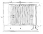
- FIG. 1is a partially-broken perspective diagram of a conventional active matrix type liquid crystal display.
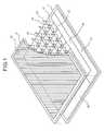
- FIG. 2is a cross-section of key portions of the conventional active matrix type liquid crystal display.
- pixel electrodes 11 and TFT's 12as switching elements are disposed in a matrix shape of m rows and n columns on a substrate (“TFT substrate”) 1.
- Electrodes that are common (“common electrodes”) 21are uniformly provided substantially on the whole surface a substrate (“common substrate”) 2.
- a liquid crystal layer 3is sealed into between the TFT substrate 1 and the common substrate 2 by a sealing section 31 .
- a plurality of data lines 13 and a plurality of scanning lines 14are provided in lengthwise and crosswise on the TFT substrate 1 , and the TFT's 12 are connected to these points of intersection.
- a part of or the whole driving circuit of the data lines 13 or the scanning lines 14are manufactured on the TFT substrate 1 , as the carrier mobility of the polysilicon TFT's is large.
- a data line driving circuit 15 and a scanning line driving circuit 16are provided on the TFT substrate 1 .
- An electrode 17 that becomes an outgoing lineis provided on the peripheral area of the TFT substrate 1 .
- a common electrode voltageis applied to the common electrodes 21 via this electrode 17 and a conductor (a transfer) 18 that is connected to this electrode 17 .
- the electrode 17is covered with a protection film 19 .
- a driving system(a common inversion driving system) that minimizes the amplitude of a voltage supplied to the data line 13 , by inverting the polarity of the common electrode voltage.
- the amplitude of a voltage applied to the data lines 13is restricted to a range of within 5 V, and the common electrode voltage is changed to match the polarity inversion period. Based on this, it becomes possible to restrict the power source voltage of the data line driving circuit 15 to 5V, for example. Therefore, it is possible to lower the withstanding voltage and the power consumption of the elements of the data line driving circuit 15 , which is advantageous in the aspect of cost and power consumption.
- the conventional liquid crystal displayhas had a problem that it is difficult to inversely drive the common electrodes 21 , and that flicker also occurs.
- the liquid crystal displaycomprises a first substrate on which pixel electrodes are disposed in a matrix shape of m rows and n columns, a second substrate on which a plurality of common electrodes are disposed in a stripe shape corresponding to the n columns of electrodes, a liquid crystal layer provided between the first substrate and the second substrate, a common electrode driving circuit provided on the first substrate, and which applies mutually-inverted voltages to the common electrodes of odd-number orders and to the common electrodes of even-number orders respectively, first conductors which electrically connect the common electrode driving circuit to the common electrodes of odd-number orders, in order to apply a voltage generated by the common electrode driving circuit to the common electrodes of odd-number orders, and second conductors which electrically connect the common electrode driving circuit to the common electrodes of even-number orders, in order to apply a voltage generated by the common electrode driving circuit to the common electrodes of even-number orders.
- the liquid crystal displaycomprises a first substrate on which pixel electrodes are disposed in a matrix shape of m rows and n columns, a second substrate on which a plurality of common electrodes are disposed in a stripe shape corresponding to the m rows of electrodes, a liquid crystal layer provided between the first substrate and the second substrate, a common electrode driving circuit provided on the first substrate, and which applies mutually-inverted voltages to the common electrodes of odd-number orders and to the common electrodes of even-number orders respectively, first conductors which electrically connect the common electrode driving circuit to the common electrodes of odd-number orders, in order to apply a voltage generated by the common electrode driving circuit to the common electrodes of odd-number orders, and second conductors which electrically connect the common electrode driving circuit to the common electrodes of even-number orders, in order to apply a voltage generated by the common electrode driving circuit to the common electrodes of even-number orders.
- the liquid crystal displaycomprises a first substrate on which pixel electrodes are disposed in a matrix shape of m rows and n columns, as a second substrate on which a plurality of first common electrodes are disposed in a stripe shape corresponding to the n columns of electrodes, and also a plurality of second common electrodes are disposed in a stripe shape corresponding to the m rows of electrodes, with the first common electrodes and the second common electrodes being insulated from each other via an insulation layer, a liquid crystal layer provided between the first substrate and the second substrate, a common electrode driving circuit provided on the first substrate, and which applies mutually-inverted voltages to the first common electrodes of odd-number orders and to the first common electrodes of even-number orders respectively, or which applies mutually-inverted voltages to the second common electrodes of odd-number orders and to the second common electrodes of even-number orders respectively, first conductors which electrically connect the common electrode driving circuit to the first common electrodes
- a common electrode voltage that is applied to a common electrode of an odd-number order and a common electrode voltage that is applied to a common electrode of an even-number orderare inverted to match the polarity inversion period respectively, by the common electrode driving circuit. Further, the common electrode voltage that is applied to a common electrode of an odd-number order and the common electrode voltage that is applied to a common electrode of an even-number order have polarities that are inverted by the common electrode driving circuit.
- FIG. 1is a partially broken-down total perspective diagram that schematically shows a conventional active matrix type liquid crystal display
- FIG. 2is a cross-sectional diagram that schematically shows a cross-sectional structure of key portions of the conventional active matrix type liquid crystal display
- FIG. 3is a top plan diagram that shows an outline of a liquid crystal display according to a first embodiment of the present invention
- FIG. 4is a waveform diagram that shows a status of changes in a common electrode voltage and a data signal of the liquid crystal display according to the first embodiment of the present invention
- FIG. 5is a top plan diagram that shows an outline of a modification of the liquid crystal display according to the first embodiment of the present invention
- FIG. 6is a top plan diagram that shows an outline of a liquid crystal display according to a second embodiment of the present invention.
- FIG. 7is a top plan diagram that shows an outline of a modification of the liquid crystal display according to the second embodiment of the present invention.
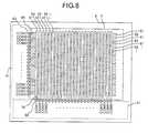
- FIG. 8is a top plan diagram that shows an outline of a liquid crystal display according to a third embodiment of the present invention.
- FIG. 3is a top plan diagram of the liquid crystal display according to a first embodiment of the present invention.
- a display sectionis provided on a TFT substrate 4 as a first substrate.
- this display sectionhas pixel electrodes and TFT's disposed in a matrix shape of m rows and n columns.
- a control circuit section 41that includes a data line driving circuit, a scanning line driving circuit, and a common electrode driving circuit.
- a common substrate 5as a second substrate that faces the display section of the TFT substrate 4 , there are disposed thin linear common electrodes 51 and 52 respectively along a plurality of data lines (not shown in the drawing) that are provided on the display section of the TFT substrate 4 .
- the data linesare extended in a lengthwise direction
- a plurality of scanning lines(not shown in the drawing) that are provided on the display section of the TFT substrate 4 are extended in a crosswise direction.
- the plurality of common electrodes 51 and 52are disposed lengthwise in a stripe shape.
- a liquid crystal layeris sealed into between the TFT substrate 4 and the common substrate 5 .
- Common electrodes of odd-number orders 51 from the left sidethat is, the common electrodes of a first order, a third order, a fifth order, etc., are connected to individual first conductors (transfers) 53 respectively.
- the plurality of first conductors 53are connected in common to a first output terminal, not shown, of the common electrode driving circuit that is provided on the control circuit section 41 of the TFT substrate 4 .
- the same common electrode voltagehereinafter, to be referred to as the COM 1
- the COM 1the same common electrode voltage
- common electrodes of even-number orders 52 from the left sidethat is, the common electrodes of a second order, a fourth order, a sixth order, etc.
- the plurality of second conductors 54are connected in common to a second output terminal, not shown, of the common electrode driving circuit. Therefore, the same common electrode voltage (hereinafter, to be referred to as the COM 2 ) is applied to the common electrodes of even-number orders 52 .
- the common electrode driving circuitgenerates a COM 1 and a COM 2 that is the inverted COM 1 . Therefore, mutually-inverted common electrode voltages are applied to the common electrodes of odd-number orders 51 and the common electrodes of even-number orders 52 respectively. Further, the common electrode driving circuit inverts the COM 1 and the COM 2 at the same time in a predetermined inversion period. The inversion period is adjusted to a period in which flicker is not noticeable.
- FIG. 4shows a status of changes in the COM 1 , the COM 2 , and a voltage applied to the data lines, that is, a change in a data signal, respectively.
- the COM 1when the COM 1 is at a relatively high voltage level, the COM 2 becomes at a relatively low voltage level.
- the COM 1when the COM 1 is at a relatively low voltage level, the COM 2 becomes at a relatively high voltage level.
- These voltage levelschange at the same timing.
- a voltage level of a data signal corresponding to the COM 1becomes at a relatively low level and in negative polarity.
- a voltage level of a data signal corresponding to the COM 1becomes at a relatively high level and in positive polarity.
- the samealso applies to the COM 2 and a data signal corresponding to the COM 2 .
- the common electrodes 51 and 52are in thin linear shapes respectively and their loads are small, it is possible to invert the COM 1 and the COM 2 at the same time in a predetermined inversion period. Therefore, it is possible to realize a common inversion driving system. Based on this, it becomes possible to make smaller the amplitude of the voltage supplied to the data lines than the amplitude of the voltage in the common fixed driving system. Consequently, it is possible to construct the data line driving circuit with elements of a low withstanding voltage. As a result, it is possible to achieve a reduction in power consumption and a reduction in cost.
- the COM 1 and the COM 2are in a mutually inverted relationship, it is possible to realize a lengthwise line inversion driving system that applies a voltage of an opposite polarity to pixels that are adjacently disposed in a crosswise direction. Therefore, based on a simultaneous realization of the common inversion driving system and the lengthwise line inversion driving system, flicker is reduced and it becomes possible to obtain satisfactory display quality in a large-screen and high-precision liquid crystal display.
- FIG. 6is a top plan diagram of the liquid crystal display according to a second embodiment of the present invention.
- the second embodimentis different from the first embodiment in that, while the common electrodes 51 and 52 are in a lengthwise stripe shape in the first embodiment, the common electrodes 61 and 62 are in a crosswise stripe shape in the second embodiment as shown in FIG. 6.
- On a common substrate 6 as a second substratethere are disposed thin linear common electrodes 61 and 62 respectively along a plurality of scanning lines (not shown in the drawing) that are provided on the display section of the TFT substrate 4 .
- common electrodes of odd-number orders 61 from the topsidethat is, the common electrodes of a first order, a third order, a fifth order, etc.
- a common electrode driving circuitprovided on a control circuit section 41 of the TFT substrate 4 via individual first conductors (transfers) 63 respectively.
- These common electrodes 61are applied with the COM 1 .
- common electrodes of even-number orders 62 from the topsidethat is, the common electrodes of a second order, a fourth order, a sixth order, etc., are electrically connected to the common electrode driving circuit via individual second conductors (transfers) 64 respectively.
- the common electrodes 61 and 62are in thin linear shapes respectively and their loads are small, it is possible to invert the COM 1 and the COM 2 at the same time in a predetermined inversion period. Therefore, it is possible to realize a common inversion driving system. Based on this, it becomes possible to make smaller the amplitude of the voltage supplied to the data lines than the amplitude of the voltage in the common fixed driving system. Consequently, it is possible to construct the data line driving circuit with elements of a low withstanding voltage. As a result, it is possible to achieve a reduction in power consumption and a reduction in cost.
- FIG. 8is a top plan diagram of the liquid crystal display according to a third embodiment of the present invention.
- the third embodimentis a combination of both structures of the first embodiment and the second embodiment.
- On a common substrate 7 as a second substratethere are disposed thin linear first common electrodes 51 and 52 respectively along a plurality of data lines (not shown in the drawing) that are provided on a display section of a TFT substrate 4 .
- On the common substrate 7there are also disposed thin linear second common electrodes 61 and 62 respectively along a plurality of scanning lines (not shown in the drawing) on this display section of the TFT substrate 4 .
- the first common electrodes 51 and 52are insulated from the second common electrodes 61 and 62 with an inter-layer insulation film.
- a first common electrode of an odd-number order 51 , a first common electrode of an even-number order 52 , a second common electrode of an odd-number order 61 , and a second common electrode of an even-number order 62are electrically connected to a common electrode driving circuit via a first conductor 53 , a second conductor 54 , a third conductor 63 , and a fourth conductor 64 respectively.
- the third embodimentwhen the first common electrodes 51 and 52 are used as the common electrodes, it is possible to realize the common inversion driving system and the lengthwise line inversion driving system at the same time.
- the second common electrodes 61 and 62when the second common electrodes 61 and 62 are used as the common electrodes, it is possible to realize the common inversion driving system and the crosswise line inversion driving system at the same time. Therefore, based on a selection of any type of the common electrodes, flicker is reduced and it becomes possible to obtain satisfactory display quality in a large-screen and high-precision liquid crystal display.
- first common electrodes 51 and 52may be electrically connected to the common electrode driving circuit via the first conductor 53 and the second conductor 54 at about one to four positions respectively. This similarly applies to the second common electrodes 61 and 62 . As a result, it becomes possible to reduce the number of connection positions at which the first to fourth conductors 53 , 54 , 63 and 64 are used.
- the application of the present inventionis not limited to a liquid crystal display that uses polysilicon TFT's, and it is also possible to apply the invention to other active matrix type liquid crystal displays.
- a common electrode voltage that is applied to a common electrode of an odd-number order and a common electrode voltage that is applied to a common electrode of an even-number orderare inverted to match the polarity inversion period respectively, by the common electrode driving circuit. Therefore, based on the realization of a common inversion driving system, it becomes possible to make smaller the amplitude of the voltage supplied to the data lines. Consequently, it is possible to construct the data line driving circuit with elements of a low withstanding voltage. As a result, there is an effect that it is possible to reduce power consumption and to reduce cost.
- the common electrode voltage that is applied to a common electrode of an odd-number order and the common electrode voltage that is applied to a common electrode of an even-number orderhave polarities that are inverted by the common electrode driving circuit. Therefore, the polarities of the voltages applied to the adjacent pixels are inverted. As a result, there is an effect that flicker is reduced, and it is possible to obtain high display quality with in a large-screen and high-precision liquid crystal display.
Landscapes
- Engineering & Computer Science (AREA)
- Power Engineering (AREA)
- Chemical & Material Sciences (AREA)
- Crystallography & Structural Chemistry (AREA)
- Physics & Mathematics (AREA)
- Computer Hardware Design (AREA)
- General Physics & Mathematics (AREA)
- Theoretical Computer Science (AREA)
- Liquid Crystal (AREA)
- Liquid Crystal Display Device Control (AREA)
- Control Of Indicators Other Than Cathode Ray Tubes (AREA)
- Devices For Indicating Variable Information By Combining Individual Elements (AREA)
Abstract
Description
- The present invention relates to an active matrix type liquid crystal display that uses a thin-film transistor (TFT).[0001]
- In general, a liquid crystal display employs an alternating current (AC) driving system that alternately applies driving voltages of positive polarity and negative polarity to liquid crystal elements of each pixel for each one frame or each one horizontal period, in order to suppress deterioration of the liquid crystal. Further, the apparatus is driven in such a way as to invert the polarities of adjacent data lines or scanning lines, in order to suppress flicker that occurs due to the AC driving system.[0002]
- FIG. 1 is a partially-broken perspective diagram of a conventional active matrix type liquid crystal display. FIG. 2 is a cross-section of key portions of the conventional active matrix type liquid crystal display. As shown in FIG. 1 and FIG. 2, in the conventional liquid crystal display,[0003]
pixel electrodes 11 and TFT's12 as switching elements are disposed in a matrix shape of m rows and n columns on a substrate (“TFT substrate”) 1. Electrodes that are common (“common electrodes”)21 are uniformly provided substantially on the whole surface a substrate (“common substrate”) 2. Aliquid crystal layer 3 is sealed into between theTFT substrate 1 and thecommon substrate 2 by asealing section 31. A plurality ofdata lines 13 and a plurality ofscanning lines 14 are provided in lengthwise and crosswise on theTFT substrate 1, and the TFT's12 are connected to these points of intersection. - According to a liquid crystal display that uses polysilicon TFT's as switching elements, usually, a part of or the whole driving circuit of the[0004]
data lines 13 or thescanning lines 14 are manufactured on theTFT substrate 1, as the carrier mobility of the polysilicon TFT's is large. As shown in FIG. 1, a dataline driving circuit 15 and a scanningline driving circuit 16 are provided on theTFT substrate 1. Anelectrode 17 that becomes an outgoing line is provided on the peripheral area of theTFT substrate 1. A common electrode voltage is applied to thecommon electrodes 21 via thiselectrode 17 and a conductor (a transfer)18 that is connected to thiselectrode 17. Theelectrode 17 is covered with aprotection film 19. - As an AC driving system of this liquid crystal display, there is a common fixed driving system that fixes a common electrode voltage to a constant value. According to this driving system, a voltage that has positive polarity and a voltage that has negative polarity relative to the common electrode voltage respectively are applied alternately to the[0005]
data lines 13. In other words, the polarity of the voltage applied to thedata lines 13 is inverted. As the amplitude of the voltage applied to thedata lines 13 becomes large, the power source voltage of the dataline driving circuit 15 becomes large. As a result, a withstanding voltage that is required for transistors, buffers, and analog switches of the dataline driving circuit 15 becomes large. Further, power consumption also increases. - There is also a driving system (a common inversion driving system) that minimizes the amplitude of a voltage supplied to the[0006]
data line 13, by inverting the polarity of the common electrode voltage. For example, the amplitude of a voltage applied to thedata lines 13 is restricted to a range of within 5 V, and the common electrode voltage is changed to match the polarity inversion period. Based on this, it becomes possible to restrict the power source voltage of the dataline driving circuit 15 to 5V, for example. Therefore, it is possible to lower the withstanding voltage and the power consumption of the elements of the dataline driving circuit 15, which is advantageous in the aspect of cost and power consumption. - However, according to the conventional liquid crystal display, the load becomes large when the sizes of the screen become large, as the[0007]
common electrode 21 are provided uniformly substantially on the whole surface of thecommon substrate 2. Therefore, the conventional liquid crystal display has had a problem that it is difficult to inversely drive thecommon electrodes 21, and that flicker also occurs. - It is an object of the present invention to provide a liquid crystal display that minimizes the occurrence of flicker and that can make a high-quality display, in the liquid crystal display that uses polysilicon TFT's.[0008]
- The liquid crystal display according to one aspect of the present invention comprises a first substrate on which pixel electrodes are disposed in a matrix shape of m rows and n columns, a second substrate on which a plurality of common electrodes are disposed in a stripe shape corresponding to the n columns of electrodes, a liquid crystal layer provided between the first substrate and the second substrate, a common electrode driving circuit provided on the first substrate, and which applies mutually-inverted voltages to the common electrodes of odd-number orders and to the common electrodes of even-number orders respectively, first conductors which electrically connect the common electrode driving circuit to the common electrodes of odd-number orders, in order to apply a voltage generated by the common electrode driving circuit to the common electrodes of odd-number orders, and second conductors which electrically connect the common electrode driving circuit to the common electrodes of even-number orders, in order to apply a voltage generated by the common electrode driving circuit to the common electrodes of even-number orders.[0009]
- The liquid crystal display according to another aspect of the present invention comprises a first substrate on which pixel electrodes are disposed in a matrix shape of m rows and n columns, a second substrate on which a plurality of common electrodes are disposed in a stripe shape corresponding to the m rows of electrodes, a liquid crystal layer provided between the first substrate and the second substrate, a common electrode driving circuit provided on the first substrate, and which applies mutually-inverted voltages to the common electrodes of odd-number orders and to the common electrodes of even-number orders respectively, first conductors which electrically connect the common electrode driving circuit to the common electrodes of odd-number orders, in order to apply a voltage generated by the common electrode driving circuit to the common electrodes of odd-number orders, and second conductors which electrically connect the common electrode driving circuit to the common electrodes of even-number orders, in order to apply a voltage generated by the common electrode driving circuit to the common electrodes of even-number orders.[0010]
- The liquid crystal display according to still another aspect of the present invention comprises a first substrate on which pixel electrodes are disposed in a matrix shape of m rows and n columns, as a second substrate on which a plurality of first common electrodes are disposed in a stripe shape corresponding to the n columns of electrodes, and also a plurality of second common electrodes are disposed in a stripe shape corresponding to the m rows of electrodes, with the first common electrodes and the second common electrodes being insulated from each other via an insulation layer, a liquid crystal layer provided between the first substrate and the second substrate, a common electrode driving circuit provided on the first substrate, and which applies mutually-inverted voltages to the first common electrodes of odd-number orders and to the first common electrodes of even-number orders respectively, or which applies mutually-inverted voltages to the second common electrodes of odd-number orders and to the second common electrodes of even-number orders respectively, first conductors which electrically connect the common electrode driving circuit to the first common electrodes of odd-number orders, in order to apply a voltage generated by the common electrode driving circuit to the first common electrodes of odd-number orders, second conductors which electrically connect the common electrode driving circuit to the first common electrodes of even-number orders, in order to apply a voltage generated by the common electrode driving circuit to the first common electrodes of even-number orders, third conductors which electrically connect the common electrode driving circuit to the second common electrodes of odd-number orders, in order to apply a voltage generated by the common electrode driving circuit to the second common electrodes of odd-number orders, and fourth conductors which electrically connect the common electrode driving circuit to the second common electrodes of even-number orders, in order to apply a voltage generated by the common electrode driving circuit to the second common electrodes of even-number orders.[0011]
- According to the above-mentioned aspects, a common electrode voltage that is applied to a common electrode of an odd-number order and a common electrode voltage that is applied to a common electrode of an even-number order are inverted to match the polarity inversion period respectively, by the common electrode driving circuit. Further, the common electrode voltage that is applied to a common electrode of an odd-number order and the common electrode voltage that is applied to a common electrode of an even-number order have polarities that are inverted by the common electrode driving circuit.[0012]
- Other objects and features of this invention will become apparent from the following description with reference to the accompanying drawings.[0013]
- FIG. 1 is a partially broken-down total perspective diagram that schematically shows a conventional active matrix type liquid crystal display,[0014]
- FIG. 2 is a cross-sectional diagram that schematically shows a cross-sectional structure of key portions of the conventional active matrix type liquid crystal display,[0015]
- FIG. 3 is a top plan diagram that shows an outline of a liquid crystal display according to a first embodiment of the present invention,[0016]
- FIG. 4 is a waveform diagram that shows a status of changes in a common electrode voltage and a data signal of the liquid crystal display according to the first embodiment of the present invention,[0017]
- FIG. 5 is a top plan diagram that shows an outline of a modification of the liquid crystal display according to the first embodiment of the present invention,[0018]
- FIG. 6 is a top plan diagram that shows an outline of a liquid crystal display according to a second embodiment of the present invention,[0019]
- FIG. 7 is a top plan diagram that shows an outline of a modification of the liquid crystal display according to the second embodiment of the present invention, and[0020]
- FIG. 8 is a top plan diagram that shows an outline of a liquid crystal display according to a third embodiment of the present invention.[0021]
- Embodiments of the liquid crystal display according to the present invention will be explained in detail below with reference to the accompanying drawings.[0022]
- FIG. 3 is a top plan diagram of the liquid crystal display according to a first embodiment of the present invention. As shown in FIG. 3, a display section is provided on a[0023]
TFT substrate 4 as a first substrate. Although not shown, this display section has pixel electrodes and TFT's disposed in a matrix shape of m rows and n columns. On the periphery of this display section, there is disposed acontrol circuit section 41 that includes a data line driving circuit, a scanning line driving circuit, and a common electrode driving circuit. - On a[0024]
common substrate 5 as a second substrate that faces the display section of theTFT substrate 4, there are disposed thin linearcommon electrodes TFT substrate 4. Assume that the data lines are extended in a lengthwise direction, and a plurality of scanning lines (not shown in the drawing) that are provided on the display section of theTFT substrate 4 are extended in a crosswise direction. Then, the plurality ofcommon electrodes TFT substrate 4 and thecommon substrate 5. - Common electrodes of odd-[0025]
number orders 51 from the left side, that is, the common electrodes of a first order, a third order, a fifth order, etc., are connected to individual first conductors (transfers)53 respectively. The plurality offirst conductors 53 are connected in common to a first output terminal, not shown, of the common electrode driving circuit that is provided on thecontrol circuit section 41 of theTFT substrate 4. In other words, the same common electrode voltage (hereinafter, to be referred to as the COM1) is applied to the common electrodes of odd-number orders 51. Furthermore, common electrodes of even-number orders 52 from the left side, that is, the common electrodes of a second order, a fourth order, a sixth order, etc., are connected to individual second conductors (transfers)54 respectively. The plurality ofsecond conductors 54 are connected in common to a second output terminal, not shown, of the common electrode driving circuit. Therefore, the same common electrode voltage (hereinafter, to be referred to as the COM2) is applied to the common electrodes of even-number orders 52. - The common electrode driving circuit generates a COM[0026]1 and a COM2 that is the inverted COM1. Therefore, mutually-inverted common electrode voltages are applied to the common electrodes of odd-
number orders 51 and the common electrodes of even-number orders 52 respectively. Further, the common electrode driving circuit inverts the COM1 and the COM2 at the same time in a predetermined inversion period. The inversion period is adjusted to a period in which flicker is not noticeable. - FIG. 4 shows a status of changes in the COM[0027]1, the COM2, and a voltage applied to the data lines, that is, a change in a data signal, respectively. As shown in FIG. 4, when the COM1 is at a relatively high voltage level, the COM2 becomes at a relatively low voltage level. When the COM1 is at a relatively low voltage level, the COM2 becomes at a relatively high voltage level. These voltage levels change at the same timing. Further, when the COM1 is at a relatively high voltage level, a voltage level of a data signal corresponding to the COM1 becomes at a relatively low level and in negative polarity. When the COM1 is at a relatively low voltage level, a voltage level of a data signal corresponding to the COM1 becomes at a relatively high level and in positive polarity. The same also applies to the COM2 and a data signal corresponding to the COM2.
- According to the first embodiment, as the[0028]
common electrodes - Further, as the COM[0029]1 and the COM2 are in a mutually inverted relationship, it is possible to realize a lengthwise line inversion driving system that applies a voltage of an opposite polarity to pixels that are adjacently disposed in a crosswise direction. Therefore, based on a simultaneous realization of the common inversion driving system and the lengthwise line inversion driving system, flicker is reduced and it becomes possible to obtain satisfactory display quality in a large-screen and high-precision liquid crystal display.
- As shown in FIG. 5, it is possible to short-circuit the common electrodes of odd-[0030]
number orders 51 by connecting them with awiring 55 on thecommon substrate 5, and to short-circuit the common electrodes of even-number orders 52 by connecting them with awiring 56 on thecommon substrate 5. Based on this arrangement, thesecommon electrodes first conductor 53 and thesecond conductor 54 at about one to four positions respectively. As a result, it becomes possible to reduce the number of connection positions at which the first andsecond conductors - FIG. 6 is a top plan diagram of the liquid crystal display according to a second embodiment of the present invention. The second embodiment is different from the first embodiment in that, while the[0031]
common electrodes common electrodes common substrate 6 as a second substrate, there are disposed thin linearcommon electrodes TFT substrate 4. - As shown in FIG. 6, common electrodes of odd-[0032]
number orders 61 from the topside, that is, the common electrodes of a first order, a third order, a fifth order, etc., are electrically connected to a common electrode driving circuit provided on acontrol circuit section 41 of theTFT substrate 4 via individual first conductors (transfers)63 respectively. Thesecommon electrodes 61 are applied with the COM1. Furthermore, common electrodes of even-number orders 62 from the topside, that is, the common electrodes of a second order, a fourth order, a sixth order, etc., are electrically connected to the common electrode driving circuit via individual second conductors (transfers)64 respectively. - Other structures are the same as those of the first embodiment. Therefore, sections of the same structures as those of the first embodiment are attached with like reference numerals, and their explanation will be omitted. Further, the status of changes in the COM[0033]1, the COM2, and a voltage level of a data signal respectively is similar to that explained in FIG. 4 and the first embodiment with reference to FIG. 4. These common electrodes are applied with the COM2.
- According to the second embodiment, as the[0034]
common electrodes - Further, as the COM[0035]1 and the COM2 are in a mutually inverted relationship, it is possible to realize a crosswise line inversion driving system that applies a voltage of an opposite polarity to pixels that are adjacently disposed in a lengthwise direction. Therefore, based on a simultaneous realization of the common inversion driving system and the crosswise line inversion driving system, flicker is reduced and it becomes possible to obtain satisfactory display quality in a large-screen and high-precision liquid crystal display.
- As shown in FIG. 7, it is possible to short-circuit the common electrodes of odd-[0036]
number orders 61 by connecting them with awiring 65 on thecommon substrate 6, and to short-circuit the common electrodes of even-number orders 62 by connecting them with awiring 66 on thecommon substrate 6. Based on this arrangement, thesecommon electrodes first conductor 63 and thesecond conductor 64 at about one to four positions respectively. As a result, it becomes possible to reduce the number of connection positions at which the first andsecond conductors - FIG. 8 is a top plan diagram of the liquid crystal display according to a third embodiment of the present invention. The third embodiment is a combination of both structures of the first embodiment and the second embodiment. On a[0037]
common substrate 7 as a second substrate, there are disposed thin linear firstcommon electrodes TFT substrate 4. At the same time, on thecommon substrate 7, there are also disposed thin linear secondcommon electrodes TFT substrate 4. - The first[0038]
common electrodes common electrodes number order 51, a first common electrode of an even-number order 52, a second common electrode of an odd-number order 61, and a second common electrode of an even-number order 62 are electrically connected to a common electrode driving circuit via afirst conductor 53, asecond conductor 54, athird conductor 63, and afourth conductor 64 respectively. - Other structures are the same as those of the first or second embodiment. Therefore, sections of the same structures as those of the first or second embodiment are attached with like reference numerals, and their explanation will be omitted. Further, the status of changes in the COM[0039]1, the COM2, and a voltage level of a data signal respectively is similar to that explained in FIG. 4 and the first embodiment with reference to FIG. 4.
- According to the third embodiment, when the first[0040]
common electrodes common electrodes - Although not particularly shown in the drawings, it is possible to mutually short-circuit the first common electrodes of odd-[0041]
number orders 51 on thecommon substrate 7, and to mutually short-circuit the first common electrodes of even-number orders 52 on thecommon substrate 7. Based on this arrangement, these firstcommon electrodes first conductor 53 and thesecond conductor 54 at about one to four positions respectively. This similarly applies to the secondcommon electrodes fourth conductors - The application of the present invention is not limited to a liquid crystal display that uses polysilicon TFT's, and it is also possible to apply the invention to other active matrix type liquid crystal displays.[0042]
- According to the present invention, a common electrode voltage that is applied to a common electrode of an odd-number order and a common electrode voltage that is applied to a common electrode of an even-number order are inverted to match the polarity inversion period respectively, by the common electrode driving circuit. Therefore, based on the realization of a common inversion driving system, it becomes possible to make smaller the amplitude of the voltage supplied to the data lines. Consequently, it is possible to construct the data line driving circuit with elements of a low withstanding voltage. As a result, there is an effect that it is possible to reduce power consumption and to reduce cost.[0043]
- Further, the common electrode voltage that is applied to a common electrode of an odd-number order and the common electrode voltage that is applied to a common electrode of an even-number order have polarities that are inverted by the common electrode driving circuit. Therefore, the polarities of the voltages applied to the adjacent pixels are inverted. As a result, there is an effect that flicker is reduced, and it is possible to obtain high display quality with in a large-screen and high-precision liquid crystal display.[0044]
- Although the invention has been described with respect to a specific embodiment for a complete and clear disclosure, the appended claims are not to be thus limited but are to be construed as embodying all modifications and alternative constructions that may occur to one skilled in the art which fairly fall within the basic teaching herein set forth.[0045]
Claims (9)
Applications Claiming Priority (2)
| Application Number | Priority Date | Filing Date | Title |
|---|---|---|---|
| JP2001-352349 | 2001-11-16 | ||
| JP2001352349AJP3917845B2 (en) | 2001-11-16 | 2001-11-16 | Liquid crystal display |
Publications (2)
| Publication Number | Publication Date |
|---|---|
| US20030095091A1true US20030095091A1 (en) | 2003-05-22 |
| US7006064B2 US7006064B2 (en) | 2006-02-28 |
Family
ID=19164540
Family Applications (1)
| Application Number | Title | Priority Date | Filing Date |
|---|---|---|---|
| US10/102,453Expired - LifetimeUS7006064B2 (en) | 2001-11-16 | 2002-03-20 | Liquid crystal display |
Country Status (2)
| Country | Link |
|---|---|
| US (1) | US7006064B2 (en) |
| JP (1) | JP3917845B2 (en) |
Cited By (30)
| Publication number | Priority date | Publication date | Assignee | Title |
|---|---|---|---|---|
| WO2003083815A3 (en)* | 2002-03-28 | 2003-12-18 | Koninkl Philips Electronics Nv | Liquid crystal display driving with dot-inversion |
| EP1646033A1 (en) | 2004-10-05 | 2006-04-12 | Research In Motion Limited | Method for maintaining the white colour point over time in a field-sequential colour LCD |
| US20080042963A1 (en)* | 2006-07-03 | 2008-02-21 | Epson Imaging Devices Corporation | Liquid crystal device, method of driving liquid crystal device, and electronic apparatus |
| US20080079680A1 (en)* | 2006-09-28 | 2008-04-03 | Epson Imaging Devices Corporation | Driving circuit and driving method of liquid crystal device, liquid crystal device, and electronic apparatus |
| US20080136801A1 (en)* | 2006-12-11 | 2008-06-12 | Innolux Display Corp. | Liquid crystal display and driving method thereof |
| US20080231572A1 (en)* | 2007-03-19 | 2008-09-25 | Innolux Display Corp. | Liquid crystal display and driving method thereof |
| EP1986182A1 (en) | 2007-04-27 | 2008-10-29 | Samsung SDI Co., Ltd. | Liquid crystal display |
| US20090002302A1 (en)* | 2007-06-28 | 2009-01-01 | Lg.Philips Lcd Co., Ltd. | Liquid crystal display and driving method thereof |
| US20090102991A1 (en)* | 2007-10-23 | 2009-04-23 | Au Optronics Corporation | Liquid Crystal Display Panel |
| US20090251445A1 (en)* | 2008-04-04 | 2009-10-08 | Sony Corporation | Driving circuit for a liquid crystal display |
| US20090251629A1 (en)* | 2008-04-04 | 2009-10-08 | Sony Corporation | Liquid crystal display module |
| US20090262061A1 (en)* | 2008-04-21 | 2009-10-22 | Infovision Optoelectronics (Kunshan) Co., Ltd. | Liquid Crystal Panel and Display Apparatus Including Liquid Crystal Panel |
| US20090284507A1 (en)* | 2008-05-16 | 2009-11-19 | Sony Corporation | Ambient light detection device |
| US20090295786A1 (en)* | 2008-05-27 | 2009-12-03 | Sony Corporation | Driving circuit for a liquid crystal display |
| CN101144954B (en)* | 2007-11-09 | 2010-06-02 | 友达光电股份有限公司 | Liquid crystal display panel and liquid crystal display |
| US20110102415A1 (en)* | 2009-10-30 | 2011-05-05 | Yoon Hyun-Sik | Display apparatus |
| US20110221726A1 (en)* | 2010-03-15 | 2011-09-15 | Hjalmar Edzer Ayco Huitema | Driving Method And System For Electrofluidic Chromatophore Pixel Display |
| US20120050243A1 (en)* | 2003-08-11 | 2012-03-01 | Sony Corporation | Display apparatus and driving method therefor |
| US20140118912A1 (en)* | 2012-11-01 | 2014-05-01 | Sipix Technology, Inc. | Display device |
| WO2015035724A1 (en)* | 2013-09-13 | 2015-03-19 | 合肥京东方光电科技有限公司 | Array substrate and drive method therefor, and display device |
| CN105372884A (en)* | 2015-12-02 | 2016-03-02 | 武汉华星光电技术有限公司 | LCD panel and electronic device using same |
| CN105467639A (en)* | 2016-01-13 | 2016-04-06 | 昆山龙腾光电有限公司 | Liquid crystal display panel and driving method thereof |
| US9601064B1 (en)* | 2011-11-28 | 2017-03-21 | Elbit Systems Ltd. | Liquid crystal display with full driver redundancy scheme |
| US20170147119A1 (en)* | 2006-06-09 | 2017-05-25 | Apple Inc. | Touch screen liquid crystal display |
| US20170177111A1 (en)* | 2015-08-13 | 2017-06-22 | Boe Technology Group Co., Ltd | Array substrate, touch screen and display apparatus containing the same, and method for driving the same |
| CN107749283A (en)* | 2017-11-06 | 2018-03-02 | 深圳市华星光电半导体显示技术有限公司 | Liquid crystal display device |
| US10331259B2 (en) | 2004-05-06 | 2019-06-25 | Apple Inc. | Multipoint touchscreen |
| US10409434B2 (en) | 2010-12-22 | 2019-09-10 | Apple Inc. | Integrated touch screens |
| US10521065B2 (en) | 2007-01-05 | 2019-12-31 | Apple Inc. | Touch screen stack-ups |
| CN113808515A (en)* | 2021-09-23 | 2021-12-17 | 惠科股份有限公司 | Common electrode structure, driving method and display device |
Families Citing this family (5)
| Publication number | Priority date | Publication date | Assignee | Title |
|---|---|---|---|---|
| US7714829B2 (en)* | 2004-10-05 | 2010-05-11 | Research In Motion Limited | Method for maintaining the white colour point in a field-sequential LCD over time |
| KR100882699B1 (en) | 2007-08-29 | 2009-02-06 | 삼성모바일디스플레이주식회사 | LCD and its driving method |
| US8259249B2 (en) | 2009-10-12 | 2012-09-04 | Samsung Electronics Co., Ltd. | Display substrate, method of manufacturing the display substrate and display device having the display substrate |
| CN102156359B (en)* | 2010-06-13 | 2014-05-07 | 京东方科技集团股份有限公司 | Array base plate, liquid crystal panel, liquid crystal display and driving method |
| CN103745704B (en)* | 2013-12-30 | 2016-06-01 | 合肥京东方光电科技有限公司 | Liquid crystal display drive circuit, Liquid Crystal Display And Method For Driving |
Citations (19)
| Publication number | Priority date | Publication date | Assignee | Title |
|---|---|---|---|---|
| US4952031A (en)* | 1987-06-19 | 1990-08-28 | Victor Company Of Japan, Ltd. | Liquid crystal display device |
| US5392058A (en)* | 1991-05-15 | 1995-02-21 | Sharp Kabushiki Kaisha | Display-integrated type tablet device |
| US5430462A (en)* | 1992-12-07 | 1995-07-04 | Sharp Kabushiki Kaisha | Image input device-integrated type display device |
| US5706022A (en)* | 1994-03-15 | 1998-01-06 | Fujitsu Limited | Optical display device having an optically transparent driver circuit |
| US5748165A (en)* | 1993-12-24 | 1998-05-05 | Sharp Kabushiki Kaisha | Image display device with plural data driving circuits for driving the display at different voltage magnitudes and polarity |
| US6078379A (en)* | 1997-06-13 | 2000-06-20 | Sharp Kabushiki Kaisha | Liquid crystal display device provided with seal material and spacer made of resist |
| US6091393A (en)* | 1997-01-08 | 2000-07-18 | Lg Electronics Inc. | Scan driver IC for a liquid crystal display |
| US6300926B1 (en)* | 1998-04-27 | 2001-10-09 | Hitachi, Ltd. | Active matrix type liquid crystal display |
| US20020008795A1 (en)* | 1995-12-19 | 2002-01-24 | Semiconductor Energy Laboratory Co., Ltd. | Active matrix liquid crystal display and method of fabricating same |
| US20020075249A1 (en)* | 2000-05-09 | 2002-06-20 | Yasushi Kubota | Data signal line drive circuit, drive circuit, image display device incorporating the same, and electronic apparatus using the same |
| US20020149323A1 (en)* | 1998-02-23 | 2002-10-17 | Seiko Epson Corporation | Method for driving an electro-optical device, driving circuit for driving an electro-optical device, electro-optical device, and electronic apparatus |
| US6489952B1 (en)* | 1998-11-17 | 2002-12-03 | Semiconductor Energy Laboratory Co., Ltd. | Active matrix type semiconductor display device |
| US20020196243A1 (en)* | 2001-06-04 | 2002-12-26 | Akira Morita | Display control circuit, electro-optical device, display device and display control method |
| US20030058208A1 (en)* | 2001-09-27 | 2003-03-27 | Tetsuya Kawamura | Liquid crystal display device and manufacturing method threreof |
| US20030117464A1 (en)* | 2001-12-20 | 2003-06-26 | Seiko Epson Corporation | Liquid-jet head and liquid-jet apparatus |
| US20030151572A1 (en)* | 2002-02-08 | 2003-08-14 | Kouji Kumada | Display device, drive circuit for the same, and driving method for the same |
| US6628258B1 (en)* | 1998-08-03 | 2003-09-30 | Seiko Epson Corporation | Electrooptic device, substrate therefor, electronic device, and projection display |
| US20030201447A1 (en)* | 2002-04-24 | 2003-10-30 | Semiconductor Energy Laboratory Co., Ltd. | Semiconductor device and method of manufacturing same |
| US20030222311A1 (en)* | 2002-05-28 | 2003-12-04 | Samsung Electronics Co., Ltd. | Amorphous silicon thin film transistor-liquid crystal display device and method of manufacturing the same |
- 2001
- 2001-11-16JPJP2001352349Apatent/JP3917845B2/ennot_activeExpired - Fee Related
- 2002
- 2002-03-20USUS10/102,453patent/US7006064B2/ennot_activeExpired - Lifetime
Patent Citations (19)
| Publication number | Priority date | Publication date | Assignee | Title |
|---|---|---|---|---|
| US4952031A (en)* | 1987-06-19 | 1990-08-28 | Victor Company Of Japan, Ltd. | Liquid crystal display device |
| US5392058A (en)* | 1991-05-15 | 1995-02-21 | Sharp Kabushiki Kaisha | Display-integrated type tablet device |
| US5430462A (en)* | 1992-12-07 | 1995-07-04 | Sharp Kabushiki Kaisha | Image input device-integrated type display device |
| US5748165A (en)* | 1993-12-24 | 1998-05-05 | Sharp Kabushiki Kaisha | Image display device with plural data driving circuits for driving the display at different voltage magnitudes and polarity |
| US5706022A (en)* | 1994-03-15 | 1998-01-06 | Fujitsu Limited | Optical display device having an optically transparent driver circuit |
| US20020008795A1 (en)* | 1995-12-19 | 2002-01-24 | Semiconductor Energy Laboratory Co., Ltd. | Active matrix liquid crystal display and method of fabricating same |
| US6091393A (en)* | 1997-01-08 | 2000-07-18 | Lg Electronics Inc. | Scan driver IC for a liquid crystal display |
| US6078379A (en)* | 1997-06-13 | 2000-06-20 | Sharp Kabushiki Kaisha | Liquid crystal display device provided with seal material and spacer made of resist |
| US20020149323A1 (en)* | 1998-02-23 | 2002-10-17 | Seiko Epson Corporation | Method for driving an electro-optical device, driving circuit for driving an electro-optical device, electro-optical device, and electronic apparatus |
| US6300926B1 (en)* | 1998-04-27 | 2001-10-09 | Hitachi, Ltd. | Active matrix type liquid crystal display |
| US6628258B1 (en)* | 1998-08-03 | 2003-09-30 | Seiko Epson Corporation | Electrooptic device, substrate therefor, electronic device, and projection display |
| US6489952B1 (en)* | 1998-11-17 | 2002-12-03 | Semiconductor Energy Laboratory Co., Ltd. | Active matrix type semiconductor display device |
| US20020075249A1 (en)* | 2000-05-09 | 2002-06-20 | Yasushi Kubota | Data signal line drive circuit, drive circuit, image display device incorporating the same, and electronic apparatus using the same |
| US20020196243A1 (en)* | 2001-06-04 | 2002-12-26 | Akira Morita | Display control circuit, electro-optical device, display device and display control method |
| US20030058208A1 (en)* | 2001-09-27 | 2003-03-27 | Tetsuya Kawamura | Liquid crystal display device and manufacturing method threreof |
| US20030117464A1 (en)* | 2001-12-20 | 2003-06-26 | Seiko Epson Corporation | Liquid-jet head and liquid-jet apparatus |
| US20030151572A1 (en)* | 2002-02-08 | 2003-08-14 | Kouji Kumada | Display device, drive circuit for the same, and driving method for the same |
| US20030201447A1 (en)* | 2002-04-24 | 2003-10-30 | Semiconductor Energy Laboratory Co., Ltd. | Semiconductor device and method of manufacturing same |
| US20030222311A1 (en)* | 2002-05-28 | 2003-12-04 | Samsung Electronics Co., Ltd. | Amorphous silicon thin film transistor-liquid crystal display device and method of manufacturing the same |
Cited By (59)
| Publication number | Priority date | Publication date | Assignee | Title |
|---|---|---|---|---|
| WO2003083815A3 (en)* | 2002-03-28 | 2003-12-18 | Koninkl Philips Electronics Nv | Liquid crystal display driving with dot-inversion |
| US8922470B2 (en)* | 2003-08-11 | 2014-12-30 | Sony Corporation | Liquid crystal display apparatus with row counter electrodes and driving method therefor |
| US20120050243A1 (en)* | 2003-08-11 | 2012-03-01 | Sony Corporation | Display apparatus and driving method therefor |
| US10908729B2 (en) | 2004-05-06 | 2021-02-02 | Apple Inc. | Multipoint touchscreen |
| US11604547B2 (en) | 2004-05-06 | 2023-03-14 | Apple Inc. | Multipoint touchscreen |
| US10331259B2 (en) | 2004-05-06 | 2019-06-25 | Apple Inc. | Multipoint touchscreen |
| EP1646033A1 (en) | 2004-10-05 | 2006-04-12 | Research In Motion Limited | Method for maintaining the white colour point over time in a field-sequential colour LCD |
| US10191576B2 (en)* | 2006-06-09 | 2019-01-29 | Apple Inc. | Touch screen liquid crystal display |
| US20170147119A1 (en)* | 2006-06-09 | 2017-05-25 | Apple Inc. | Touch screen liquid crystal display |
| US10976846B2 (en)* | 2006-06-09 | 2021-04-13 | Apple Inc. | Touch screen liquid crystal display |
| US11175762B2 (en) | 2006-06-09 | 2021-11-16 | Apple Inc. | Touch screen liquid crystal display |
| US20220057880A1 (en)* | 2006-06-09 | 2022-02-24 | Apple Inc. | Touch screen liquid crystal display |
| US11886651B2 (en)* | 2006-06-09 | 2024-01-30 | Apple Inc. | Touch screen liquid crystal display |
| US9697784B2 (en) | 2006-07-03 | 2017-07-04 | Japan Display Inc. | Liquid crystal device, method of driving liquid crystal device, and electronic apparatus |
| US9240153B2 (en)* | 2006-07-03 | 2016-01-19 | Japan Display Inc. | Liquid crystal device, method of driving liquid crystal device, and electronic apparatus |
| US20080042963A1 (en)* | 2006-07-03 | 2008-02-21 | Epson Imaging Devices Corporation | Liquid crystal device, method of driving liquid crystal device, and electronic apparatus |
| US20080079680A1 (en)* | 2006-09-28 | 2008-04-03 | Epson Imaging Devices Corporation | Driving circuit and driving method of liquid crystal device, liquid crystal device, and electronic apparatus |
| US20080136801A1 (en)* | 2006-12-11 | 2008-06-12 | Innolux Display Corp. | Liquid crystal display and driving method thereof |
| US10521065B2 (en) | 2007-01-05 | 2019-12-31 | Apple Inc. | Touch screen stack-ups |
| US20080231572A1 (en)* | 2007-03-19 | 2008-09-25 | Innolux Display Corp. | Liquid crystal display and driving method thereof |
| US8994627B2 (en) | 2007-04-27 | 2015-03-31 | Samsung Display Co., Ltd. | Liquid crystal display |
| US20080266219A1 (en)* | 2007-04-27 | 2008-10-30 | Minwoo Kim | Liquid crystal display |
| EP1986182A1 (en) | 2007-04-27 | 2008-10-29 | Samsung SDI Co., Ltd. | Liquid crystal display |
| US8026887B2 (en)* | 2007-06-28 | 2011-09-27 | Lg Display Co., Ltd. | Liquid crystal display and driving method thereof |
| US20090002301A1 (en)* | 2007-06-28 | 2009-01-01 | Lg.Philips Lcd Co., Ltd. | Liquid crystal display and driving method thereof |
| US8049698B2 (en)* | 2007-06-28 | 2011-11-01 | Lg Display Co., Ltd. | Liquid crystal display and driving method thereof |
| US20090002302A1 (en)* | 2007-06-28 | 2009-01-01 | Lg.Philips Lcd Co., Ltd. | Liquid crystal display and driving method thereof |
| US20090102991A1 (en)* | 2007-10-23 | 2009-04-23 | Au Optronics Corporation | Liquid Crystal Display Panel |
| CN101144954B (en)* | 2007-11-09 | 2010-06-02 | 友达光电股份有限公司 | Liquid crystal display panel and liquid crystal display |
| US20090251629A1 (en)* | 2008-04-04 | 2009-10-08 | Sony Corporation | Liquid crystal display module |
| EP2107549A3 (en)* | 2008-04-04 | 2010-09-22 | Sony Corporation | Liquid crystal display module |
| US20090251445A1 (en)* | 2008-04-04 | 2009-10-08 | Sony Corporation | Driving circuit for a liquid crystal display |
| US8456398B2 (en) | 2008-04-04 | 2013-06-04 | Sony Corporation | Liquid crystal display module |
| US20090262061A1 (en)* | 2008-04-21 | 2009-10-22 | Infovision Optoelectronics (Kunshan) Co., Ltd. | Liquid Crystal Panel and Display Apparatus Including Liquid Crystal Panel |
| US8537084B2 (en) | 2008-04-21 | 2013-09-17 | Infovision Optoelectronics (Kunshan) Co., Ltd. | Liquid crystal panel and display apparatus including liquid crystal panel |
| US20090284507A1 (en)* | 2008-05-16 | 2009-11-19 | Sony Corporation | Ambient light detection device |
| US8355014B2 (en) | 2008-05-16 | 2013-01-15 | Sony Corporation | Ambient light detection device |
| US20090295786A1 (en)* | 2008-05-27 | 2009-12-03 | Sony Corporation | Driving circuit for a liquid crystal display |
| US8963822B2 (en) | 2009-10-30 | 2015-02-24 | Samsung Display Co., Ltd. | Display apparatus |
| EP2317502A3 (en)* | 2009-10-30 | 2014-07-09 | Samsung Display Co., Ltd. | Display apparatus |
| US20110102415A1 (en)* | 2009-10-30 | 2011-05-05 | Yoon Hyun-Sik | Display apparatus |
| US20110221726A1 (en)* | 2010-03-15 | 2011-09-15 | Hjalmar Edzer Ayco Huitema | Driving Method And System For Electrofluidic Chromatophore Pixel Display |
| US8547325B2 (en)* | 2010-03-15 | 2013-10-01 | Creator Technology B.V. | Driving method and system for electrofluidic chromatophore pixel display |
| US10409434B2 (en) | 2010-12-22 | 2019-09-10 | Apple Inc. | Integrated touch screens |
| US9601064B1 (en)* | 2011-11-28 | 2017-03-21 | Elbit Systems Ltd. | Liquid crystal display with full driver redundancy scheme |
| US20140118912A1 (en)* | 2012-11-01 | 2014-05-01 | Sipix Technology, Inc. | Display device |
| CN103809344B (en)* | 2012-11-01 | 2016-08-17 | 达意科技股份有限公司 | Display device |
| CN103809344A (en)* | 2012-11-01 | 2014-05-21 | 达意科技股份有限公司 | Display device |
| US9201279B2 (en)* | 2012-11-01 | 2015-12-01 | Sipix Technology, Inc. | Display device |
| US9812079B2 (en) | 2013-09-13 | 2017-11-07 | Boe Technology Group Co., Ltd. | Array substrate, driving method thereof and display apparatus |
| WO2015035724A1 (en)* | 2013-09-13 | 2015-03-19 | 合肥京东方光电科技有限公司 | Array substrate and drive method therefor, and display device |
| US20170177111A1 (en)* | 2015-08-13 | 2017-06-22 | Boe Technology Group Co., Ltd | Array substrate, touch screen and display apparatus containing the same, and method for driving the same |
| US10209836B2 (en)* | 2015-08-13 | 2019-02-19 | Boe Technology Group Co., Ltd. | Array substrate, touch screen and display apparatus containing the same, and method for driving the same |
| CN105372884A (en)* | 2015-12-02 | 2016-03-02 | 武汉华星光电技术有限公司 | LCD panel and electronic device using same |
| WO2017092134A1 (en)* | 2015-12-02 | 2017-06-08 | 武汉华星光电技术有限公司 | Liquid crystal display panel and electronic device employing the liquid crystal display panel |
| CN105467639A (en)* | 2016-01-13 | 2016-04-06 | 昆山龙腾光电有限公司 | Liquid crystal display panel and driving method thereof |
| CN107749283A (en)* | 2017-11-06 | 2018-03-02 | 深圳市华星光电半导体显示技术有限公司 | Liquid crystal display device |
| CN113808515A (en)* | 2021-09-23 | 2021-12-17 | 惠科股份有限公司 | Common electrode structure, driving method and display device |
| US11645962B2 (en) | 2021-09-23 | 2023-05-09 | HKC Corporation Limited | Common electrode pattern, driving method, and display equipment |
Also Published As
| Publication number | Publication date |
|---|---|
| JP3917845B2 (en) | 2007-05-23 |
| JP2003149670A (en) | 2003-05-21 |
| US7006064B2 (en) | 2006-02-28 |
Similar Documents
| Publication | Publication Date | Title |
|---|---|---|
| US7006064B2 (en) | Liquid crystal display | |
| JP4031291B2 (en) | Liquid crystal display | |
| CA2047905C (en) | Liquid crystal display | |
| CA2046357C (en) | Liquid crystal display | |
| US8194201B2 (en) | Display panel and liquid crystal display including the same | |
| US10228595B2 (en) | Display device with layered wiring structure for external connection | |
| US7986296B2 (en) | Liquid crystal display and its driving method | |
| US7321352B2 (en) | Liquid crystal display and method for driving the same | |
| KR101641958B1 (en) | Liquid crsytal display | |
| KR20050113907A (en) | Liquid crystal display device and driving method for the same | |
| US7557786B2 (en) | Display device | |
| KR20040020317A (en) | liquid crystal device and method thereof | |
| WO2011049106A1 (en) | Liquid crystal display device | |
| US20070097052A1 (en) | Liquid crystal display device | |
| KR20010015385A (en) | Active matrix type liquid crystal display apparatus | |
| JP2007188089A (en) | Liquid crystal display | |
| US9646553B2 (en) | Display device | |
| KR101725341B1 (en) | Liquid crsytal display | |
| TW200302369A (en) | Liquid crystal display device | |
| CN111142298A (en) | Array substrate and display device | |
| JP2010032974A (en) | Liquid crystal display device | |
| JP4702114B2 (en) | Demultiplexer, electro-optical device and electronic apparatus | |
| CN109188816B (en) | Array substrate and driving method thereof, and liquid crystal display device and driving method thereof | |
| US6670936B1 (en) | Liquid crystal display | |
| US20040004606A1 (en) | Image display element and image display device |
Legal Events
| Date | Code | Title | Description |
|---|---|---|---|
| AS | Assignment | Owner name:FUJITSU LIMITED, JAPAN Free format text:ASSIGNMENT OF ASSIGNORS INTEREST;ASSIGNORS:ENOMOTO, HIROMI;OKAZAKI, SUSUMU;ZHANG, HONGYONG;REEL/FRAME:012734/0553 Effective date:20020315 | |
| AS | Assignment | Owner name:FUJITSU DISPLAY TECHNOLOGIES CORPORATION, JAPAN Free format text:ASSIGNMENT OF ASSIGNORS INTEREST;ASSIGNOR:FUJITSU LIMITED;REEL/FRAME:013552/0107 Effective date:20021024 Owner name:FUJITSU DISPLAY TECHNOLOGIES CORPORATION,JAPAN Free format text:ASSIGNMENT OF ASSIGNORS INTEREST;ASSIGNOR:FUJITSU LIMITED;REEL/FRAME:013552/0107 Effective date:20021024 | |
| AS | Assignment | Owner name:FUJITSU LIMITED,JAPAN Free format text:ASSIGNMENT OF ASSIGNORS INTEREST;ASSIGNOR:FUJITSU DISPLAY TECHNOLOGIES CORPORATION;REEL/FRAME:016345/0310 Effective date:20050630 Owner name:FUJITSU LIMITED, JAPAN Free format text:ASSIGNMENT OF ASSIGNORS INTEREST;ASSIGNOR:FUJITSU DISPLAY TECHNOLOGIES CORPORATION;REEL/FRAME:016345/0310 Effective date:20050630 | |
| AS | Assignment | Owner name:SHARP KABUSHIKI KAISHA,JAPAN Free format text:ASSIGNMENT OF ASSIGNORS INTEREST;ASSIGNOR:FUJITSU LIMITED;REEL/FRAME:016345/0210 Effective date:20050701 Owner name:SHARP KABUSHIKI KAISHA, JAPAN Free format text:ASSIGNMENT OF ASSIGNORS INTEREST;ASSIGNOR:FUJITSU LIMITED;REEL/FRAME:016345/0210 Effective date:20050701 | |
| STCF | Information on status: patent grant | Free format text:PATENTED CASE | |
| CC | Certificate of correction | ||
| FEPP | Fee payment procedure | Free format text:PAYOR NUMBER ASSIGNED (ORIGINAL EVENT CODE: ASPN); ENTITY STATUS OF PATENT OWNER: LARGE ENTITY | |
| FPAY | Fee payment | Year of fee payment:4 | |
| FPAY | Fee payment | Year of fee payment:8 | |
| FEPP | Fee payment procedure | Free format text:PAYOR NUMBER ASSIGNED (ORIGINAL EVENT CODE: ASPN); ENTITY STATUS OF PATENT OWNER: LARGE ENTITY Free format text:PAYER NUMBER DE-ASSIGNED (ORIGINAL EVENT CODE: RMPN); ENTITY STATUS OF PATENT OWNER: LARGE ENTITY | |
| MAFP | Maintenance fee payment | Free format text:PAYMENT OF MAINTENANCE FEE, 12TH YEAR, LARGE ENTITY (ORIGINAL EVENT CODE: M1553) Year of fee payment:12 |