US20030092218A1 - Deflectable interconnect - Google Patents
Deflectable interconnectDownload PDFInfo
- Publication number
- US20030092218A1 US20030092218A1US10/324,627US32462702AUS2003092218A1US 20030092218 A1US20030092218 A1US 20030092218A1US 32462702 AUS32462702 AUS 32462702AUS 2003092218 A1US2003092218 A1US 2003092218A1
- Authority
- US
- United States
- Prior art keywords
- solder
- integrated circuit
- interposer
- conductive
- package
- Prior art date
- Legal status (The legal status is an assumption and is not a legal conclusion. Google has not performed a legal analysis and makes no representation as to the accuracy of the status listed.)
- Granted
Links
- 229910000679solderInorganic materials0.000claimsabstractdescription198
- 238000000034methodMethods0.000claimsdescription51
- 239000000853adhesiveSubstances0.000claimsdescription50
- 230000001070adhesive effectEffects0.000claimsdescription50
- 239000010410layerSubstances0.000claimsdescription19
- 239000000463materialSubstances0.000claimsdescription9
- 239000012790adhesive layerSubstances0.000claimsdescription7
- 238000010438heat treatmentMethods0.000claimsdescription7
- 239000004593EpoxySubstances0.000claimsdescription2
- 239000002657fibrous materialSubstances0.000claimsdescription2
- 239000011810insulating materialSubstances0.000claimsdescription2
- -1thermoplastSubstances0.000claimsdescription2
- 229920001169thermoplasticPolymers0.000claimsdescription2
- 239000004416thermosoftening plasticSubstances0.000claimsdescription2
- 230000003213activating effectEffects0.000claims2
- 230000002708enhancing effectEffects0.000claims1
- 230000009977dual effectEffects0.000description24
- 239000004020conductorSubstances0.000description21
- 239000000758substrateSubstances0.000description18
- 238000010521absorption reactionMethods0.000description5
- 238000005530etchingMethods0.000description4
- 238000004519manufacturing processMethods0.000description4
- RYGMFSIKBFXOCR-UHFFFAOYSA-NCopperChemical compound[Cu]RYGMFSIKBFXOCR-UHFFFAOYSA-N0.000description3
- 238000004891communicationMethods0.000description3
- 229910052802copperInorganic materials0.000description3
- 239000010949copperSubstances0.000description3
- 238000000151depositionMethods0.000description3
- PCHJSUWPFVWCPO-UHFFFAOYSA-NgoldChemical compound[Au]PCHJSUWPFVWCPO-UHFFFAOYSA-N0.000description3
- 229910052737goldInorganic materials0.000description3
- 239000010931goldSubstances0.000description3
- 230000008018meltingEffects0.000description3
- 238000002844meltingMethods0.000description3
- 230000015572biosynthetic processEffects0.000description2
- 230000000694effectsEffects0.000description2
- 239000004033plasticSubstances0.000description2
- 229910045601alloyInorganic materials0.000description1
- 239000000956alloySubstances0.000description1
- XAGFODPZIPBFFR-UHFFFAOYSA-NaluminiumChemical compound[Al]XAGFODPZIPBFFR-UHFFFAOYSA-N0.000description1
- 229910052782aluminiumInorganic materials0.000description1
- 238000003491arrayMethods0.000description1
- 230000008021depositionEffects0.000description1
- 238000005553drillingMethods0.000description1
- 238000005516engineering processMethods0.000description1
- 230000007613environmental effectEffects0.000description1
- 230000007246mechanismEffects0.000description1
- 239000000203mixtureSubstances0.000description1
- 238000012986modificationMethods0.000description1
- 230000004048modificationEffects0.000description1
- 229920000642polymerPolymers0.000description1
- 238000004080punchingMethods0.000description1
- 238000007650screen-printingMethods0.000description1
- 239000004065semiconductorSubstances0.000description1
- 239000002356single layerSubstances0.000description1
- 239000000126substanceSubstances0.000description1
- 238000006467substitution reactionMethods0.000description1
Images


Classifications
- H—ELECTRICITY
- H01—ELECTRIC ELEMENTS
- H01L—SEMICONDUCTOR DEVICES NOT COVERED BY CLASS H10
- H01L24/00—Arrangements for connecting or disconnecting semiconductor or solid-state bodies; Methods or apparatus related thereto
- H01L24/01—Means for bonding being attached to, or being formed on, the surface to be connected, e.g. chip-to-package, die-attach, "first-level" interconnects; Manufacturing methods related thereto
- H01L24/10—Bump connectors ; Manufacturing methods related thereto
- H01L24/15—Structure, shape, material or disposition of the bump connectors after the connecting process
- H01L24/16—Structure, shape, material or disposition of the bump connectors after the connecting process of an individual bump connector
- H—ELECTRICITY
- H01—ELECTRIC ELEMENTS
- H01L—SEMICONDUCTOR DEVICES NOT COVERED BY CLASS H10
- H01L23/00—Details of semiconductor or other solid state devices
- H01L23/48—Arrangements for conducting electric current to or from the solid state body in operation, e.g. leads, terminal arrangements ; Selection of materials therefor
- H01L23/488—Arrangements for conducting electric current to or from the solid state body in operation, e.g. leads, terminal arrangements ; Selection of materials therefor consisting of soldered or bonded constructions
- H01L23/498—Leads, i.e. metallisations or lead-frames on insulating substrates, e.g. chip carriers
- H01L23/49811—Additional leads joined to the metallisation on the insulating substrate, e.g. pins, bumps, wires, flat leads
- H—ELECTRICITY
- H01—ELECTRIC ELEMENTS
- H01L—SEMICONDUCTOR DEVICES NOT COVERED BY CLASS H10
- H01L23/00—Details of semiconductor or other solid state devices
- H01L23/48—Arrangements for conducting electric current to or from the solid state body in operation, e.g. leads, terminal arrangements ; Selection of materials therefor
- H01L23/488—Arrangements for conducting electric current to or from the solid state body in operation, e.g. leads, terminal arrangements ; Selection of materials therefor consisting of soldered or bonded constructions
- H01L23/498—Leads, i.e. metallisations or lead-frames on insulating substrates, e.g. chip carriers
- H01L23/4985—Flexible insulating substrates
- H—ELECTRICITY
- H05—ELECTRIC TECHNIQUES NOT OTHERWISE PROVIDED FOR
- H05K—PRINTED CIRCUITS; CASINGS OR CONSTRUCTIONAL DETAILS OF ELECTRIC APPARATUS; MANUFACTURE OF ASSEMBLAGES OF ELECTRICAL COMPONENTS
- H05K3/00—Apparatus or processes for manufacturing printed circuits
- H05K3/30—Assembling printed circuits with electric components, e.g. with resistor
- H05K3/32—Assembling printed circuits with electric components, e.g. with resistor electrically connecting electric components or wires to printed circuits
- H05K3/325—Assembling printed circuits with electric components, e.g. with resistor electrically connecting electric components or wires to printed circuits by abutting or pinching, i.e. without alloying process; mechanical auxiliary parts therefor
- H05K3/326—Assembling printed circuits with electric components, e.g. with resistor electrically connecting electric components or wires to printed circuits by abutting or pinching, i.e. without alloying process; mechanical auxiliary parts therefor the printed circuit having integral resilient or deformable parts, e.g. tabs or parts of flexible circuits
- H—ELECTRICITY
- H01—ELECTRIC ELEMENTS
- H01L—SEMICONDUCTOR DEVICES NOT COVERED BY CLASS H10
- H01L2224/00—Indexing scheme for arrangements for connecting or disconnecting semiconductor or solid-state bodies and methods related thereto as covered by H01L24/00
- H01L2224/01—Means for bonding being attached to, or being formed on, the surface to be connected, e.g. chip-to-package, die-attach, "first-level" interconnects; Manufacturing methods related thereto
- H01L2224/10—Bump connectors; Manufacturing methods related thereto
- H01L2224/12—Structure, shape, material or disposition of the bump connectors prior to the connecting process
- H01L2224/13—Structure, shape, material or disposition of the bump connectors prior to the connecting process of an individual bump connector
- H01L2224/13001—Core members of the bump connector
- H01L2224/13099—Material
- H—ELECTRICITY
- H01—ELECTRIC ELEMENTS
- H01L—SEMICONDUCTOR DEVICES NOT COVERED BY CLASS H10
- H01L2224/00—Indexing scheme for arrangements for connecting or disconnecting semiconductor or solid-state bodies and methods related thereto as covered by H01L24/00
- H01L2224/01—Means for bonding being attached to, or being formed on, the surface to be connected, e.g. chip-to-package, die-attach, "first-level" interconnects; Manufacturing methods related thereto
- H01L2224/10—Bump connectors; Manufacturing methods related thereto
- H01L2224/15—Structure, shape, material or disposition of the bump connectors after the connecting process
- H01L2224/16—Structure, shape, material or disposition of the bump connectors after the connecting process of an individual bump connector
- H01L2224/161—Disposition
- H01L2224/16151—Disposition the bump connector connecting between a semiconductor or solid-state body and an item not being a semiconductor or solid-state body, e.g. chip-to-substrate, chip-to-passive
- H01L2224/16221—Disposition the bump connector connecting between a semiconductor or solid-state body and an item not being a semiconductor or solid-state body, e.g. chip-to-substrate, chip-to-passive the body and the item being stacked
- H01L2224/16225—Disposition the bump connector connecting between a semiconductor or solid-state body and an item not being a semiconductor or solid-state body, e.g. chip-to-substrate, chip-to-passive the body and the item being stacked the item being non-metallic, e.g. insulating substrate with or without metallisation
- H01L2224/16237—Disposition the bump connector connecting between a semiconductor or solid-state body and an item not being a semiconductor or solid-state body, e.g. chip-to-substrate, chip-to-passive the body and the item being stacked the item being non-metallic, e.g. insulating substrate with or without metallisation the bump connector connecting to a bonding area disposed in a recess of the surface of the item
- H—ELECTRICITY
- H01—ELECTRIC ELEMENTS
- H01L—SEMICONDUCTOR DEVICES NOT COVERED BY CLASS H10
- H01L2924/00—Indexing scheme for arrangements or methods for connecting or disconnecting semiconductor or solid-state bodies as covered by H01L24/00
- H01L2924/01—Chemical elements
- H01L2924/01005—Boron [B]
- H—ELECTRICITY
- H01—ELECTRIC ELEMENTS
- H01L—SEMICONDUCTOR DEVICES NOT COVERED BY CLASS H10
- H01L2924/00—Indexing scheme for arrangements or methods for connecting or disconnecting semiconductor or solid-state bodies as covered by H01L24/00
- H01L2924/01—Chemical elements
- H01L2924/01006—Carbon [C]
- H—ELECTRICITY
- H01—ELECTRIC ELEMENTS
- H01L—SEMICONDUCTOR DEVICES NOT COVERED BY CLASS H10
- H01L2924/00—Indexing scheme for arrangements or methods for connecting or disconnecting semiconductor or solid-state bodies as covered by H01L24/00
- H01L2924/01—Chemical elements
- H01L2924/01013—Aluminum [Al]
- H—ELECTRICITY
- H01—ELECTRIC ELEMENTS
- H01L—SEMICONDUCTOR DEVICES NOT COVERED BY CLASS H10
- H01L2924/00—Indexing scheme for arrangements or methods for connecting or disconnecting semiconductor or solid-state bodies as covered by H01L24/00
- H01L2924/01—Chemical elements
- H01L2924/01027—Cobalt [Co]
- H—ELECTRICITY
- H01—ELECTRIC ELEMENTS
- H01L—SEMICONDUCTOR DEVICES NOT COVERED BY CLASS H10
- H01L2924/00—Indexing scheme for arrangements or methods for connecting or disconnecting semiconductor or solid-state bodies as covered by H01L24/00
- H01L2924/01—Chemical elements
- H01L2924/01029—Copper [Cu]
- H—ELECTRICITY
- H01—ELECTRIC ELEMENTS
- H01L—SEMICONDUCTOR DEVICES NOT COVERED BY CLASS H10
- H01L2924/00—Indexing scheme for arrangements or methods for connecting or disconnecting semiconductor or solid-state bodies as covered by H01L24/00
- H01L2924/01—Chemical elements
- H01L2924/01033—Arsenic [As]
- H—ELECTRICITY
- H01—ELECTRIC ELEMENTS
- H01L—SEMICONDUCTOR DEVICES NOT COVERED BY CLASS H10
- H01L2924/00—Indexing scheme for arrangements or methods for connecting or disconnecting semiconductor or solid-state bodies as covered by H01L24/00
- H01L2924/01—Chemical elements
- H01L2924/01079—Gold [Au]
- H—ELECTRICITY
- H01—ELECTRIC ELEMENTS
- H01L—SEMICONDUCTOR DEVICES NOT COVERED BY CLASS H10
- H01L2924/00—Indexing scheme for arrangements or methods for connecting or disconnecting semiconductor or solid-state bodies as covered by H01L24/00
- H01L2924/013—Alloys
- H01L2924/014—Solder alloys
- H—ELECTRICITY
- H01—ELECTRIC ELEMENTS
- H01L—SEMICONDUCTOR DEVICES NOT COVERED BY CLASS H10
- H01L2924/00—Indexing scheme for arrangements or methods for connecting or disconnecting semiconductor or solid-state bodies as covered by H01L24/00
- H01L2924/10—Details of semiconductor or other solid state devices to be connected
- H01L2924/11—Device type
- H01L2924/14—Integrated circuits
- H—ELECTRICITY
- H01—ELECTRIC ELEMENTS
- H01L—SEMICONDUCTOR DEVICES NOT COVERED BY CLASS H10
- H01L2924/00—Indexing scheme for arrangements or methods for connecting or disconnecting semiconductor or solid-state bodies as covered by H01L24/00
- H01L2924/15—Details of package parts other than the semiconductor or other solid state devices to be connected
- H01L2924/151—Die mounting substrate
- H01L2924/153—Connection portion
- H01L2924/1531—Connection portion the connection portion being formed only on the surface of the substrate opposite to the die mounting surface
- H01L2924/15311—Connection portion the connection portion being formed only on the surface of the substrate opposite to the die mounting surface being a ball array, e.g. BGA
- H—ELECTRICITY
- H05—ELECTRIC TECHNIQUES NOT OTHERWISE PROVIDED FOR
- H05K—PRINTED CIRCUITS; CASINGS OR CONSTRUCTIONAL DETAILS OF ELECTRIC APPARATUS; MANUFACTURE OF ASSEMBLAGES OF ELECTRICAL COMPONENTS
- H05K3/00—Apparatus or processes for manufacturing printed circuits
- H05K3/30—Assembling printed circuits with electric components, e.g. with resistor
- H05K3/32—Assembling printed circuits with electric components, e.g. with resistor electrically connecting electric components or wires to printed circuits
- H05K3/34—Assembling printed circuits with electric components, e.g. with resistor electrically connecting electric components or wires to printed circuits by soldering
- H05K3/341—Surface mounted components
- H05K3/3431—Leadless components
- H05K3/3436—Leadless components having an array of bottom contacts, e.g. pad grid array or ball grid array components
- H—ELECTRICITY
- H05—ELECTRIC TECHNIQUES NOT OTHERWISE PROVIDED FOR
- H05K—PRINTED CIRCUITS; CASINGS OR CONSTRUCTIONAL DETAILS OF ELECTRIC APPARATUS; MANUFACTURE OF ASSEMBLAGES OF ELECTRICAL COMPONENTS
- H05K3/00—Apparatus or processes for manufacturing printed circuits
- H05K3/40—Forming printed elements for providing electric connections to or between printed circuits
- H05K3/4092—Integral conductive tabs, i.e. conductive parts partly detached from the substrate
Definitions
- the present inventionrelates in general to integrated circuit packages and more particularly to ball grid array (BGA) packages.
- BGAball grid array
- a typical BGA packageincludes an IC affixed to a flexible polymide tape.
- a very thin conductor or wire bondconnects a pad on the IC to a conductive trace on the polymide tape.
- the conductive traceis routed to a solder ball.
- the solder ballis one of an array of solder balls that connect to the opposite side of the polymide tape and protrude from the bottom of the BGA package. These solder balls interconnect with an array of pads located on a substrate, such as a printed circuit board. Accordingly, the typical BGA package electrically connects each pad on an IC to a pad on a printed circuit board.
- Typical BGA packageshave drawbacks arising from the different coefficients of thermal expansion for the IC and the polymide tape.
- the coefficient of thermal expansion of a materialcorresponds to the degree in which the material will expand when heated and contract when cooled.
- the wire bondexperiences stress and tension. Such stress and tension may cause the wire bond to loosen or break, thereby disconnecting the IC from the printed circuit board.
- a flip chip packageincludes an IC affixed to a polymide tape with a thick adhesive such that the pads of the IC are positioned over a layer of conductive traces. Gaps in the adhesive provide room for a plurality of solder bumps that are used to connect the pads of the IC to the conductive traces. Similar to the typical BGA package, the conductive traces are routed to downward facing solder balls, which connect with pads of a substrate, such as a printed circuit board.
- the solder bumps of the flip chip packageprovide an electrical connection from the pads of the IC to the layer of conductive traces.
- the solder bump and adhesive dimensionsneed to be matched with a great deal of accuracy.
- the solder bump diameteris small as compared to the thickness of the adhesive, the solder bump cannot connect the pads of the IC to the conductive traces.
- the solder bump diameteris large as compared to the thickness of the adhesive, then the adhesive layer cannot sufficiently affix the IC to the tape.
- air pockets or bubblescan form. These air pockets not only make for a poor electrical connection, but also further exacerbate the relatively narrow tolerances allowed for the solder bump and adhesive.
- One aspect of the inventionis to provide a package having an electrical connection between an IC and an interposer.
- the packagecomprises a solder bump, a solder ball, and an interconnect having a deflectable cantilever.
- the solder bumpapplies surface tension to the deflectable cantilever, thereby causing the cantilever to deflect downward.
- the solder bumpis heated and the solder reflows, the reflowing solder releases the surface tension on the cantilever.
- the cantileverthen springs back toward its original position, within the reflowing solder. Thus, the reflowing solder partially absorbs the cantilever.
- use of a deflectable cantileveradvantageously provides for greater absorption of the interconnect into the solder, thereby reducing the possible effects of air pockets.
- use of a larger diameter solder bumpadvantageously provides more solder, thereby also reducing the possible effects of air pockets.
- the ball grid array packageinterconnects a plurality of solder bumps on an integrated circuit with a plurality of solder balls located on the exterior of the ball grid array package.
- the ball grid array packagecomprises at least one solder bump attached to an integrated circuit and at least one solder ball which is configured to interface with a printed circuit board.
- the ball grid array packagefurther comprises an interposer with at least one pocket and at least one via, wherein the pocket is configured to receive the solder bump and wherein the via is configured to receive the solder ball.
- the ball grid array packagefurther comprises a conductive interconnect circuit which electrically interconnects the solder ball in the via with the solder bump in the pocket.
- the conductive interconnect circuitfurther comprises at least one deflectable cantilever which extends into the pocket such that the deflectable cantilever is partially absorbed by the solder bump in the pocket.
- One embodiment of the inventionrelates to an integrated circuit package that comprises at least one solder connection attached to an integrated circuit.
- the integrated circuit packagefurther comprises a substrate with an opening which is configured to receive the solder connection attached to the integrated circuit.
- the integrated circuit packagealso comprises a resilient cantilever which extends into the opening such that the resilient cantilever applies pressure to the solder connection during reflow.
- Another embodiment of the inventionrelates to an apparatus that comprises an interconnect layer with a first opening.
- the apparatusfurther comprises a conductor layered above the interconnect layer.
- the conductorcomprising a deformable portion that extends into the first opening, wherein the deformable portion has resiliency that urges the deformable portion into a solder connection.
- An additional embodimentrelates to an integrated circuit package that comprises a first solder connection in communication with an integrated circuit.
- the integrated circuit packagefurther comprises an interconnect layer having a first opening.
- the integrated circuit packagealso comprises a conductor layered above the interconnect layer. The conductor comprising a deflectable portion that extends into the first opening, wherein the deflectable portion has resiliency that urges the deflectable portion into the solder connection during reflow.
- One embodiment of the inventionrelates to an apparatus comprising a substrate with an opening.
- the apparatusfurther comprising a conductive layer above the interconnect layer.
- the conductive layercomprising at least two malleable portions which extend into the opening.
- a packagecomprises an integrated circuit having a pad and a solder connection in communication with the pad.
- the packagefurther comprises a partially deflected first conductor and a partially deflected second conductor. The partially deflected first and second conductors each at least partially absorbed by the solder connection.
- an apparatuscomprises a substrate with an opening.
- the apparatusfurther comprises a conductive layer above the interconnect layer.
- the conductive layercomprising at least two flaps which extend into the opening.
- Yet another embodimentrelates to a package that comprises an integrated circuit having a pad and a solder bump in communication with the pad.
- the packagefurther comprises a deflectable conductor having partially deflected multiple flaps.
- the partially deflected multiple flapsare at least partially absorbed by the solder bump, wherein the absorption of the partially deflected multiple flaps is caused by the partially deflected multiple flaps moving from a deflected position toward a non-deflected position when the solder bump reflows.
- One embodiment of the inventionrelates to a package for an integrated circuit that comprises an adhesive having a thickness and a solder bump having a diameter greater than the adhesive thickness.
- the packagefurther comprises a conductive trace having a deflectable cantilever, wherein the deflectable cantilever deflects into a pocket when the adhesive layer affixes the integrated circuit to the conductive trace.
- the cantileveralso springs toward its original position when the solder bump reflows.
- the packagealso comprises a solder ball and a tape attached between the conductive trace and the solder ball.
- Another embodiment of the inventionrelates to a method for forming a package for an integrated circuit that comprises attaching a solder bump to an integrated circuit and forming a pocket in an interposer.
- the methodfurther comprises tracing an interconnect over the interposer such that a deflectable portion of the interconnect extends over a portion of the pocket.
- the methodalso comprises affixing the integrated circuit to the interposer such that the solder bump deflects the deflectable portion of the interconnect into the pocket.
- An additional embodimentrelates to a method for forming a package for an integrated circuit.
- the methodcomprises heating a solder bump to at least partially melt the solder bump.
- the methodfurther comprises allowing a deflectable portion of an interconnect to spring toward a non-deflected position of the deflectable portion.
- the methodalso comprises partially absorbing the deflectable portion into the solder of the solder bump.
- Yet another embodiment of the inventionrelates to a method for forming a package for an integrated circuit.
- the methodcomprises forming an interconnect with at least two resilient conductors.
- the methodfurther comprises deflecting the two resilient conductors with solder and heating the solder to at least partially melt the solder.
- the methodalso comprises allowing the two resilient conductors to spring into at least a portion of the solder.
- One embodiment of the inventionrelates to a method for forming a package for an, integrated circuit.
- the methodcomprises forming an interconnect with at least one deflectable flap and deflecting the flap with solder.
- the methodfurther comprises heating the solder to at least partially melt the solder and allowing the flap to be absorbed by at least a portion of the solder bump.
- Another embodiment of the inventionrelates to a method for forming an electrical connection between solder and a conductive material.
- the methodcomprises using solder to apply a surface tension on a deflectable portion of a conductive material, thereby deflecting the deflectable portion.
- the methodfurther comprises heating the solder beyond a melting point, thereby substantially reducing the surface tension on the deflectable portion.
- the methodalso comprises partially absorbing the deflectable portion into the solder as the deflectable portion springs back toward its approximate original position.
- An additional embodiment of the inventionrelates to a method for forming an electrical connection between solder and a conductive material.
- the methodcomprises using solder to deflect a cantilever and heating the solder beyond a melting point.
- the methodfurther comprises partially absorbing the cantilever into the solder as the cantilever springs back toward a non-deflected position.
- Yet another embodiment of the inventionrelates to a method for forming an electrical connection between solder and a conductive material.
- the methodcomprises using solder to deflect a cantilever from a first position to a second position and heating the solder beyond a melting point.
- the methodfurther comprises at least partially absorbing the cantilever into the solder such that the cantilever moves from a second position to a third position.
- One embodiment of the inventionrelates to a device that comprises means for affixing an integrated circuit to a conductive layer.
- the devicefurther comprises means for deflecting the conductive layer and then partially absorbing the conductive layer, thereby electrically connecting the integrated circuit to the conductive layer.
- FIG. 1Ais an exploded view of an electrical device, in accordance with one embodiment of the invention.
- FIG. 1Bis a cross-sectional view of the electrical device of FIG. 1A;
- FIG. 2is a cross-sectional view of a package having a deflectable cantilever, prior to attachment of an IC, according to another embodiment
- FIG. 3is a top view of the deflectable cantilever of FIG. 2;
- FIG. 4is a cross-sectional view of the package of FIG. 2, after attachment of the IC;
- FIG. 5is a cross-sectional view of the package of FIG. 2, after reflow of the solder bump;
- FIG. 6is a cross-sectional view of a package having dual deflectable cantilevers, prior to attachment of an IC, according to yet another embodiment
- FIG. 7is a top view of the dual deflectable cantilevers of FIG. 6;
- FIG. 8is a cross-sectional view of the package of FIG. 6, after attachment of the IC;
- FIG. 9is a cross-sectional view of the package of FIG. 6, after reflow of the solder bump.
- FIG. 10is a top view of a multi-flap cantilever, according to yet another embodiment.
- the disclosed deflectable cantileverWhile illustrated in the context of forming an electrical connection between an IC and an interposer, the skilled artisan will find application for the deflectable cantilever disclosed herein in a wide variety of contexts.
- the disclosed deflectable cantileverhas utility in providing an electrical connection when solder is used as a conductor, such as within a BGA package.
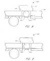
- FIGS. 1A and 1Billustrate an electrical device 100 , including a package 105 , and a substrate 110 .
- FIG. 1Aillustrates an exploded view of the electrical device 100
- FIG. 1Billustrates a cross sectional view of the same.
- the electrical device 100finds use in a wide variety of applications.
- the package 105can be used in any electronic circuit needing the attachment of an integrated circuit or the die 115 to the substrate 110 , such as the attachment of a microprocessor to a printed circuit board.
- the package 105comprises the die 115 , pads 120 , solder bumps 125 , an adhesive 130 , an interposer 135 having interconnects 140 , and solder balls 145 .
- the die 115will be understood by one of ordinary skill in the art to be any integrated circuit.
- the die 115can be from a wide range of integrated circuit products, such as: microprocessors, co-processors, digital signal processors, graphics processors, microcontrollers, memory devices, reprogrammable devices, programmable logic devices, and logic arrays.
- the die 115comprises a memory device.
- the pads 120are shown in broken lines to indicate that they are on the reverse side of the die 115 .
- the pads 120electrically connect the die 115 to a variety of other devices, signals, or other “off chip” systems. It will be understood by one of skill in the art of semiconductor package design that throughout the disclosure, the number of pads 120 , solder bumps 125 , interposer 135 , interconnects 140 , solder balls 145 , etc. are illustrated for clarity with only a few examples. In reality, there may be many pads 120 on the die 115 .
- commercially available memory devices from Micron Technology, Inc.include a 60-pin DRAM and a 100-pin SRAM, having 60 and 100 pads, respectively.
- the pads 120are electrically connected to the solder bumps 125 .
- Such connectioncan be by commercially available processes, such as those offered by Flip Chip Tech.
- the solder bumps 125are small approximate spheres of solder. However, it will be understood that a wide variety of shapes could be used. For example, the solder bumps 125 could be in the shape of a pin or a cylinder or be any type of solder connection.
- the package 105includes the adhesive 130 for affixing the die 115 to the interposer 135 and the interconnects 140 .
- the adhesive 130includes a number of adhesive gaps or adhesive pockets 133 , which make room for the solder bumps 125 .
- the adhesive 130should also be strong enough to properly affix the die 115 to the interposer 135 and the interconnects 140 , such that the solder bumps 125 deflect a portion of the interconnects 140 , as discussed in more detail below.
- the adhesive 130comprises a thermal plastic polymer, however, it will be understood that the adhesive 130 can be a variety of products.
- the adhesive 130can comprise any thermal set, thermal plastic, or any adhesive. Such products are commercially available from various manufactures such as: Ablestik, Sumioxy, Dow Coming, and Hitachi.
- the interconnects 140are conductive paths or traces from the physical locations of the solder bumps 125 to the physical locations of the solder balls 145 .
- the interconnects 140are a resilient, yet malleable conductive material such that they provide spring or memory as well as conductivity. For example, when a surface tension is placed on the interconnects 140 , they should deflect in a direction corresponding to the surface tension. When the surface tension is removed, the interconnects 140 “spring” back in the direction of their original position.
- a wide variety of conductive materialsexhibit such properties.
- the interconnects 140include gold plated copper. However, it is understood that other conductive materials and combinations are also suitable, such as, but not limited to, copper, gold, aluminum, and various alloys.
- the interconnects 140can also comprise a wide variety of trace patterns, in a wide variety of sizes and layers.
- the interconnects 140trace from the physical positions of the solder bumps 125 to the physical positions of the solder balls 145 along a single layer.
- multiple layers of the interconnects 140could trace through multiple layers of the interposer 135 in order to provide sufficient physical space for the amount of the interconnects 140 needed to correspond to the amount of pads 120 on the die 115 .
- the interposer 135provides on one side a surface upon which the interconnects 140 are traced, and on the other side a connecting point for the solder balls 145 .
- the interposer 135is a flexible “tape” substrate comprising insulating material, such as polymide tape. It is understood that other substrates could also be used, such as thermoplastic, thermoplast, epoxy, flex circuits, printed circuit board materials, or fiber materials. Polymide tape and analogous materials are commercially available from Shinko, Sumitomo, Compass, 3M, Casio, Packard-Hughes, Hitachi Cable, Cicorel, Shindo, Mitsui MS, and Rite Flex.
- the interposer 135includes the vias 150 for attaching the solder balls 145 to the interconnects 140 .
- the vias 150correspond. to a predefined pattern of the solder balls 145 for the package 105 .
- Using pre-defined patterns for the solder balls 145allows the output mechanisms, e.g., the solder balls 145 , to remain constant over changing patterns of the pads 120 corresponding to changing the die 115 .
- the interposer 135is customized on the side facing the interconnects 140 .
- the interposer 135would be customized by the tracing of the interconnects 140 from the pre-defined pattern of the vias 150 to corresponding physical locations of the pads 120 on the die 115 .
- the pattern of the solder balls 145need not be pre-defined. Rather, the interposer 135 could have a pre-defined pattern for the physical location of the pads 120 , and use the interconnects 140 to trace to the vias 150 connected to a customized pattern of the solder balls 145 . Alternatively, the interconnects 140 could connect customized patterns for both the pads 120 and the solder balls 145 .
- the interposer 135includes deflection pockets 155 .
- the deflection pockets 155exist on the interconnect-facing side of the interposer 135 .
- Deflectable portions, or cantilevers 160of the interconnects 140 , extend above the deflection pockets 155 such that when surface tension is applied to the tops of the cantilevers 160 , it causes the cantilevers 160 to deflect downward into the deflection pockets 155 .
- the package 105is mounted on the substrate 110 , where the substrate 110 comprises a printed circuit board.
- the substrate 110could comprise a wide variety of materials for a wide variety of applications.
- the substrate 110is a printed circuit board.
- the substratecan include a wide variety of materials including, but not limited to BT and FR 4 .
- the substrate 110includes conductive traces 165 electrically connected to substrate pads 170 .
- the substrate pads 170are configured to correspond to, or match with, the physical location of the solder balls 145 .
- the conductive traces 165trace an electrical connection from the substrate pads 170 to any number of “off chip” systems or signals.
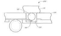
- FIGS. 2 - 5illustrate a package 200 , according to another embodiment of the invention.
- FIGS. 2 and 4illustrate a process of combining elements of the package 200 in order to deflect the cantilever 160 into a deflection pocket 155
- FIG. 3illustrates a top view of the cantilever 160
- FIG. 5illustrates the package 200 after reflow of the solder in the solder bump 125 .
- FIGS. 2 - 5illustrate only one electrical connection made from the die 115 , through the solder bump 125 and interconnect 140 , to the solder ball 145 .
- the die 115may have many electrical connections through many solder bumps 125 and interconnects 140 , to many solder balls 145 .
- FIG. 2illustrates a cross-sectional view of the package 200 before attachment of the die 115 .
- the solder bump 125is attached to the die 115 .
- the interposer 135 , the interconnect 160 and the adhesive 130are configured to receive the. solder bump 125 and the die 115 .
- the interposer 135comprises the via 150 and the deflection pocket 155 .
- the solder ball 145has not yet been attached to the via 150 . However, it will be understood that the solder ball 145 could be attached and therefore, the solder ball 145 is shown in broken lines in FIGS. 2 , 4 - 6 , and 8 - 9 .
- the interconnect 140is constructed by depositing gold plated copper on to the interposer 135 . Conventional etching techniques are then used to create a desired pattern for the interconnect 140 . In certain embodiments, the interconnect 140 is traced on the die-facing side of the interconnect 140 . As discussed in further detail below, the interconnect 140 can include a cantilever 160 . The skilled artisan will recognize that the interconnect 140 can be a wide range of conductors, conductive traces or the like. Furthermore, the cantilever 160 can in certain embodiments include deflectable portions, resilient portions, deformable portions, or malleable portions of the interconnect 140 .
- the adhesive 130attaches the interposer 135 and the interconnect 140 to the die 115 .
- the adhesive 130is selected such that it can withstand a temperature of at least about 150 EC, for example, Sumioxy LOC Tape, manufactured by Occidental Chemical Corporation.
- the adhesive layer 130comprises at least one adhesive pocket 133 .
- the adhesive pocket 133extends through the adhesive layer 130 and partially into the interposer 135 .
- the adhesive pockets 133are holes that extend through the adhesive layer 130 and the interposer 135 .
- the adhesive pocket 133is dimensioned to receive the solder bump 125 .
- the adhesive pocket 133is constructed by selectively applying adhesive to the interconnect 140 and the interposer 135 using known techniques.
- the adhesive pocket 133is constructed by screen printing, drilling or punching the adhesive layer 130 or interposer 135 .
- FIG. 3illustrates a top view of the interposer 135 and the interconnect 140 .
- the interposer 135includes the deflection pocket 155 surrounded by the interconnect 140 .
- the deflection pocket 155is approximately square in shape and does not extend entirely through the interposer 135 .
- a wide variety of shapescould be used to form the deflection pocket 155 , for example, approximately circular, oval, or polygonal shapes could be used.
- a wide variety of shapes of the interconnect 140could be used to surround the deflection pocket 155 .
- the shapes of the interconnect 140could either correspond to, or be different from, the wide variety of shapes of the deflection pocket 155 .
- the deflection pocket 155could be polygonal in shape and be surrounded by the interconnect 140 in a circular fashion.
- the deflection pocket 155could extend entirely through the interposer 135 thereby creating another hole or via in the interposer 135 . While such a punched-through deflection pocket 155 is typically easier to manufacture, it can expose the interior of the package 200 to environmental conditions after the die 115 and the solder ball 125 are attached.
- FIG. 3also illustrates the cantilever 160 extending over the deflection pocket 155 .
- the cantilever 160extends approximately half the distance across the deflection pocket 155 .
- the pattern of the interconnect 140is shown deposited on a portion of the interposer 135 and over the defection pocket 155 . It will be understood by one of skill in the art that the pattern of the interconnect 140 can be adapted for a variety of patterns and situations.
- FIG. 4illustrates a cross-sectional view of the package 200 , after the die 115 and the solder bump 125 are affixed to the adhesive 130 .
- the diameter of the solder bump 125is larger than the thickness of the adhesive 130 , and therefore, the solder bump 125 applies a surface tension to the cantilever 160 .
- the surface tensiondeflects the cantilever 160 downward into the deflection pocket 155 .
- the resilient deflected cantilever 160applies a pressure on the solder bump 125 that is directed towards the surface of the solder bump 125 .
- FIG. 5illustrates a cross-sectional view of the package 200 after reflow of the solder in the solder bump 125 .
- the solder in the solder bump 125reflows, it applies less surface tension to the cantilever 160 , allowing the cantilever 160 to spring back in the direction of the original position of the cantilever 160 .
- the cantilever 160returns, it is at least partially absorbed by the reflowing solder.
- the cantilever 160applies an inwardly directed pressure to the solder bump 125 the urges the cantilever 160 into the solder bump 125 .
- the die 115could have a variety of sizes and thicknesses.
- the die 115can be from a wide range of integrated circuit products. For this reason, the type of integrated circuit product will dictate the thickness of the die 115 .
- the die 115is a dynamic memory device with a thickness of approximately 280 microns.
- the thickness of the interconnect 140 and the cantilever 160is approximately 15 microns
- the thickness of the interposer 135is approximately 48 microns
- the diameter of the solder ball 145is approximately 400 microns.
- the diameter of the solder bump 125 and the thickness of the adhesive 130can vary over wider ranges. For example, when the diameter of the solder bump 125 is larger than the thickness of the adhesive 130 , the cantilever 160 is deflected into the deflection pocket 155 . Thus, in order to create an electrical connection, the diameter of the solder bump 125 in the package 200 can be as thick or thicker than the adhesive 130 . In one embodiment, the diameter of the solder bump 125 is approximately 200 microns and the thickness of the adhesive 130 is approximately 176 microns.
- FIGS. 2 - 5thus provides the package 200 that has electrical connections from the pads 120 on the die 115 , through the solder bumps 125 and the interconnects 140 , to the solder balls 145 .
- the solder bumps 125deflect the cantilevers 160 when the die 115 is affixed to the adhesive 130 .
- the cantilevers 160spring back toward their original position and are thereby partially absorbed by the solder bump 125 .
- Deflectionallows for relaxed tolerance requirements between the diameter of the solder bump 125 and the thickness of the adhesive 130 . Partial absorption allows for formation of an electrical connection. These characteristics improve yield rates and thereby decrease the cost of package manufacture.
- FIGS. 6 - 9illustrate a package 600 according to yet another embodiment of the invention.
- FIGS. 6 and 8illustrate a process of combining elements of the package 600 in order to deflect dual cantilevers 605 and 610 into a deflection pocket 615
- FIG. 7illustrates a top view of the dual cantilevers 605 and 610
- FIG. 9illustrates the package 600 after reflow of the solder in the solder bump 125 .
- FIGS. 6 - 9illustrate only one electrical connection made from the die 115 , through the solder bump 125 and interconnect 140 , to the solder ball 145 .
- the die 115may have many electrical connections through many solder bumps 125 and interconnects 140 , to many solder balls 145 .
- FIG. 6illustrates a cross-sectional view of the package 600 before attachment of the die 115 .
- the solder bump 125is attached to the die 115 .
- the interposer 135includes the interconnect 140 traced on at least the die-facing side of the interposer 135 .
- the interconnect 140is deposited on the interposer 135 . Typical etching techniques are used to create a desired pattern for the interconnect 140 .
- the interposer 135also includes the via 150 and the deflection pocket 615 .
- the solder ball 145has not yet been attached to the via 150 .
- the adhesive 130is then added in order to cover both the interposer 135 and the interconnect 140 .
- the adhesive pockets 133are added, punched, drilled and screen printed.
- the pocket 615 and the via 150comprise openings formed in the interposer 135 .
- FIG. 7illustrates a top view of the interposer 135 and the interconnect 140 .
- the interposer 135includes the deflection pocket 615 surrounded by the interconnect 140 .
- the deflection pocket 615is approximately square in shape and does not extend entirely through the interposer 135 .
- a wide variety of shapescould be used to form the deflection pocket 615 .
- a wide variety of shapes of the interconnect 140could be used to surround the deflection pocket 615 .
- the deflection pocket 615could be polygonal in shape and be surrounded by the interconnect 140 in a circular fashion.
- FIG. 7also illustrates the deflection pocket 615 as an alternative to the deflection pocket 155 of FIGS. 2 - 5 .
- the deflection pocket 615extends through the interposer 135 . It will be understood that a skilled artisan would recognize that the deflection pocket 615 could be used with the embodiment of FIGS. 2 - 5 , and likewise, the deflection pocket 155 could be adapted for use in FIG. 6.
- FIG. 7also illustrates the dual cantilevers 605 and 610 extending over the deflection pocket 615 from opposite sides.
- Each of the dual cantilevers 605 and 610is similar in composition and material considerations as those mentioned in reference to the cantilever 160 .
- each of the dual cantilevers 605 and 610has a length which is approximately half the diameter or width of the deflection pocket 615 .
- the first cantilever 605may be approximately a third of the width of the deflection pocket 615 while the second cantilever 610 may be approximately two-thirds the width of the deflection pocket 615 .
- the dual cantilevers 605 and 610may each be less than approximately half the width of the deflection pocket 615 .
- the dual cantilevers 605 and 610may have a lower bound on their lengths being dictated only by the desire for some deflection therein.
- the dual cantilevers 605 and 610may be of different lengths in order to exhibit different deflection distances. Thereby, the dual cantilever 605 and 610 would be absorbed into different areas of the solder bump 125 .
- the dual cantilevers 605 and 610could have lengths longer than half the diameter, or half the width, of the deflection pocket 615 by being offset from direct opposition of each other.
- a skilled artisanmay use other designs for the dual cantilevers 605 and 610 directed to needs recognizable to such an artisan.
- one skilled in the artcould manipulate the flexibility and spring constant of each of the dual cantilevers 605 and 610 by adjusting the widths and lengths thereof.
- FIG. 8illustrates a cross-sectional view of the package 600 , after the die 115 and the solder bump 125 are affixed to the adhesive 130 .
- the diameter of the solder bump 125is larger than the thickness of the adhesive 130 , and therefore, the solder bump 125 applies a surface tension to the dual cantilevers 605 and 610 .
- the surface tensiondeflects the dual cantilevers 605 and 610 downward into the deflection pocket 615 .
- FIG. 9illustrates a cross-sectional view of the package 600 after reflow of the solder in the solder bump 125 .
- the solder in the solder bump 125reflows, it applies less surface tension to the dual cantilevers 605 and 610 , allowing each of the dual cantilevers 605 and 610 to spring back in the direction of their original position.
- the dual cantilevers 605 and 610return, they are at least partially absorbed by the reflowing solder. Partial absorption creates an electrical connection in spite of possible air pockets or bubbles.
- the dual cantilevers 605 and 610 in the package 600allows the diameter of the solder bump 125 and the thickness of the adhesive 130 to have a more relaxed relationship. For example, when the diameter of the solder bump 125 is larger than the thickness of the adhesive 130 , the dual cantilevers 605 and 610 are deflected into the deflection pocket 615 . Thus, in order to create an electrical connection, the diameter of the solder bump 125 in the package 600 need only be as thick as the adhesive 130 . On the other hand, the diameter of the solder bump 125 may be as large as the maximum deflection of the dual cantilevers 605 and 605 . In one embodiment, the diameter of the solder bump 125 is approximately 200 microns and the thickness of the adhesive 130 is approximately 176 microns.
- FIGS. 6 - 9thus provides the package 600 that has electrical connections from the pads 120 on the die 115 , through the solder bumps 125 and the interconnects 140 , to the solder balls 145 .
- the solder bumps 125deflect the dual cantilevers 605 and 610 when the die 115 is affixed to the adhesive 130 .
- the dual cantilevers 605 and 610spring back toward their approximate original position and are thereby partially absorbed by the solder bumps 125 .
- Deflectionallows for relaxed tolerance requirements between the diameter of the solder bumps 125 and the thickness of the adhesive 130 . Partial absorption allows for formation of an electrical connection. These characteristics improve yield rates and thereby decrease the cost of package manufacture.
- FIG. 10illustrates a top view of yet another embodiment of the invention. Similar to FIGS. 3 and 7, FIG. 10 includes the interposer 135 having a deflection pocket 1010 (shown in broken lines) surrounded by the interconnect 140 . As with the deflection pocket 155 , it will be understood that the deflection pocket 1010 could be many shapes and the interconnect 140 may or may not correspond to such shapes. Furthermore, the deflection pocket 1010 could extend entirely through the interposer 135 . However, in one embodiment, the deflection pocket 1010 is approximately square and extends only partially through the interposer 135 .
- the interconnect 140includes a series of flaps 1005 extending over and partially covering the deflection pocket 1010 .
- the flaps 1005are made by depositing the interconnect 140 over the deflection pocket 1010 and then etching openings 1015 therein. The deposition and etching are done by typical methods known to one of ordinary skill in the art of package design.
- the openings 1015define the shape of the flaps 1005 and provide the ability of the flaps 1005 to deflect downward into the deflection pocket 1010 . It will be understood that the flaps 1005 could be a wide variety of shapes and sizes. However, in one embodiment, the flaps 1005 comprise four triangular-shaped flaps 1005 , with each of the flaps 1005 having one vertice in the approximate center of the deflection pocket 1010 .
Landscapes
- Engineering & Computer Science (AREA)
- Microelectronics & Electronic Packaging (AREA)
- Computer Hardware Design (AREA)
- Power Engineering (AREA)
- Physics & Mathematics (AREA)
- Condensed Matter Physics & Semiconductors (AREA)
- General Physics & Mathematics (AREA)
- Metallurgy (AREA)
- Manufacturing & Machinery (AREA)
- Electric Connection Of Electric Components To Printed Circuits (AREA)
- Wire Bonding (AREA)
Abstract
Description
- This present application is a divisional of U.S. application Ser. No. 09/929,616, filed on Aug. 14, 2001, entitled “DEFLECTABLE INTERCONNECT,” which is a divisional of U.S. application Ser. No. 09/352,802, now U.S. Pat. No. 6,285,081, filed Jul. 13, 1999, entitled “DEFLECTABLE INTERCONNECT” The present application incorporates the foregoing disclosures herein by reference.[0001]
- 1. Field of the Invention[0002]
- The present invention relates in general to integrated circuit packages and more particularly to ball grid array (BGA) packages.[0003]
- 2. Background[0004]
- An increasing consideration in the design and use of integrated circuits is the package in which the integrated circuit (IC) resides. As ICs become more complex, and printed circuit boards become more crowded, IC packages continually need more leads or pins while their footprints consume smaller and smaller areas. In an effort to meet these demands, developers created the ball grid array (BGA) package.[0005]
- A typical BGA package includes an IC affixed to a flexible polymide tape. A very thin conductor or wire bond connects a pad on the IC to a conductive trace on the polymide tape. The conductive trace is routed to a solder ball. The solder ball is one of an array of solder balls that connect to the opposite side of the polymide tape and protrude from the bottom of the BGA package. These solder balls interconnect with an array of pads located on a substrate, such as a printed circuit board. Accordingly, the typical BGA package electrically connects each pad on an IC to a pad on a printed circuit board.[0006]
- Typical BGA packages have drawbacks arising from the different coefficients of thermal expansion for the IC and the polymide tape. In general, the coefficient of thermal expansion of a material corresponds to the degree in which the material will expand when heated and contract when cooled. As the IC and the polymide tape expand and contract at different rates, the wire bond experiences stress and tension. Such stress and tension may cause the wire bond to loosen or break, thereby disconnecting the IC from the printed circuit board.[0007]
- To compensate for stress and tension caused by thermal expansion, designers have developed IC packages without wire bonds. One conventional package is a “flip chip” package. A flip chip package includes an IC affixed to a polymide tape with a thick adhesive such that the pads of the IC are positioned over a layer of conductive traces. Gaps in the adhesive provide room for a plurality of solder bumps that are used to connect the pads of the IC to the conductive traces. Similar to the typical BGA package, the conductive traces are routed to downward facing solder balls, which connect with pads of a substrate, such as a printed circuit board.[0008]
- Accordingly, the solder bumps of the flip chip package provide an electrical connection from the pads of the IC to the layer of conductive traces. Unfortunately, several drawbacks of these packages can prevent a good electrical connection from happening. For example, the solder bump and adhesive dimensions need to be matched with a great deal of accuracy. When the solder bump diameter is small as compared to the thickness of the adhesive, the solder bump cannot connect the pads of the IC to the conductive traces. On the other hand, when the solder bump diameter is large as compared to the thickness of the adhesive, then the adhesive layer cannot sufficiently affix the IC to the tape. Furthermore, when the solder bumps are heated to cause the solder to reflow, air pockets or bubbles can form. These air pockets not only make for a poor electrical connection, but also further exacerbate the relatively narrow tolerances allowed for the solder bump and adhesive.[0009]
- These drawbacks can cause the loss of an electrical connection between the IC pads and the conductive traces. Such loss lowers yield rates, which in turn increases the overall cost of package manufacture.[0010]
- One aspect of the invention is to provide a package having an electrical connection between an IC and an interposer. The package comprises a solder bump, a solder ball, and an interconnect having a deflectable cantilever. When the IC is affixed to the interconnect, the solder bump applies surface tension to the deflectable cantilever, thereby causing the cantilever to deflect downward. When the solder bump is heated and the solder reflows, the reflowing solder releases the surface tension on the cantilever. According to one aspect of the invention, the cantilever then springs back toward its original position, within the reflowing solder. Thus, the reflowing solder partially absorbs the cantilever.[0011]
- In one embodiment, use of a deflectable cantilever advantageously provides for greater absorption of the interconnect into the solder, thereby reducing the possible effects of air pockets. In another embodiment, use of a larger diameter solder bump advantageously provides more solder, thereby also reducing the possible effects of air pockets.[0012]
- Another aspect of the invention relates to a ball grid array package for an integrated circuit. The ball grid array package interconnects a plurality of solder bumps on an integrated circuit with a plurality of solder balls located on the exterior of the ball grid array package. The ball grid array package comprises at least one solder bump attached to an integrated circuit and at least one solder ball which is configured to interface with a printed circuit board. The ball grid array package further comprises an interposer with at least one pocket and at least one via, wherein the pocket is configured to receive the solder bump and wherein the via is configured to receive the solder ball.[0013]
- The ball grid array package further comprises a conductive interconnect circuit which electrically interconnects the solder ball in the via with the solder bump in the pocket. The conductive interconnect circuit further comprises at least one deflectable cantilever which extends into the pocket such that the deflectable cantilever is partially absorbed by the solder bump in the pocket.[0014]
- One embodiment of the invention relates to an integrated circuit package that comprises at least one solder connection attached to an integrated circuit. The integrated circuit package further comprises a substrate with an opening which is configured to receive the solder connection attached to the integrated circuit. The integrated circuit package also comprises a resilient cantilever which extends into the opening such that the resilient cantilever applies pressure to the solder connection during reflow.[0015]
- Another embodiment of the invention relates to an apparatus that comprises an interconnect layer with a first opening. The apparatus further comprises a conductor layered above the interconnect layer. The conductor comprising a deformable portion that extends into the first opening, wherein the deformable portion has resiliency that urges the deformable portion into a solder connection.[0016]
- An additional embodiment relates to an integrated circuit package that comprises a first solder connection in communication with an integrated circuit. The integrated circuit package further comprises an interconnect layer having a first opening. The integrated circuit package also comprises a conductor layered above the interconnect layer. The conductor comprising a deflectable portion that extends into the first opening, wherein the deflectable portion has resiliency that urges the deflectable portion into the solder connection during reflow.[0017]
- One embodiment of the invention relates to an apparatus comprising a substrate with an opening. The apparatus further comprising a conductive layer above the interconnect layer. The conductive layer comprising at least two malleable portions which extend into the opening. In another embodiment a package comprises an integrated circuit having a pad and a solder connection in communication with the pad. The package further comprises a partially deflected first conductor and a partially deflected second conductor. The partially deflected first and second conductors each at least partially absorbed by the solder connection.[0018]
- In an additional embodiment, an apparatus comprises a substrate with an opening. The apparatus further comprises a conductive layer above the interconnect layer. The conductive layer comprising at least two flaps which extend into the opening. Yet another embodiment relates to a package that comprises an integrated circuit having a pad and a solder bump in communication with the pad. The package further comprises a deflectable conductor having partially deflected multiple flaps. The partially deflected multiple flaps are at least partially absorbed by the solder bump, wherein the absorption of the partially deflected multiple flaps is caused by the partially deflected multiple flaps moving from a deflected position toward a non-deflected position when the solder bump reflows.[0019]
- One embodiment of the invention relates to a package for an integrated circuit that comprises an adhesive having a thickness and a solder bump having a diameter greater than the adhesive thickness. The package further comprises a conductive trace having a deflectable cantilever, wherein the deflectable cantilever deflects into a pocket when the adhesive layer affixes the integrated circuit to the conductive trace. The cantilever also springs toward its original position when the solder bump reflows. The package also comprises a solder ball and a tape attached between the conductive trace and the solder ball.[0020]
- Another embodiment of the invention relates to a method for forming a package for an integrated circuit that comprises attaching a solder bump to an integrated circuit and forming a pocket in an interposer. The method further comprises tracing an interconnect over the interposer such that a deflectable portion of the interconnect extends over a portion of the pocket. The method also comprises affixing the integrated circuit to the interposer such that the solder bump deflects the deflectable portion of the interconnect into the pocket.[0021]
- An additional embodiment relates to a method for forming a package for an integrated circuit. The method comprises heating a solder bump to at least partially melt the solder bump. The method further comprises allowing a deflectable portion of an interconnect to spring toward a non-deflected position of the deflectable portion. The method also comprises partially absorbing the deflectable portion into the solder of the solder bump.[0022]
- Yet another embodiment of the invention relates to a method for forming a package for an integrated circuit. The method comprises forming an interconnect with at least two resilient conductors. The method further comprises deflecting the two resilient conductors with solder and heating the solder to at least partially melt the solder. The method also comprises allowing the two resilient conductors to spring into at least a portion of the solder.[0023]
- One embodiment of the invention relates to a method for forming a package for an, integrated circuit. The method comprises forming an interconnect with at least one deflectable flap and deflecting the flap with solder. The method further comprises heating the solder to at least partially melt the solder and allowing the flap to be absorbed by at least a portion of the solder bump.[0024]
- Another embodiment of the invention relates to a method for forming an electrical connection between solder and a conductive material. The method comprises using solder to apply a surface tension on a deflectable portion of a conductive material, thereby deflecting the deflectable portion. The method further comprises heating the solder beyond a melting point, thereby substantially reducing the surface tension on the deflectable portion. The method also comprises partially absorbing the deflectable portion into the solder as the deflectable portion springs back toward its approximate original position.[0025]
- An additional embodiment of the invention relates to a method for forming an electrical connection between solder and a conductive material. The method comprises using solder to deflect a cantilever and heating the solder beyond a melting point. The method further comprises partially absorbing the cantilever into the solder as the cantilever springs back toward a non-deflected position.[0026]
- Yet another embodiment of the invention relates to a method for forming an electrical connection between solder and a conductive material. The method comprises using solder to deflect a cantilever from a first position to a second position and heating the solder beyond a melting point. The method further comprises at least partially absorbing the cantilever into the solder such that the cantilever moves from a second position to a third position.[0027]
- One embodiment of the invention relates to a device that comprises means for affixing an integrated circuit to a conductive layer. The device further comprises means for deflecting the conductive layer and then partially absorbing the conductive layer, thereby electrically connecting the integrated circuit to the conductive layer.[0028]
- For, purposes of summarizing the invention, certain aspects, advantages and novel features of the invention have been described herein above. Of course, it is to be understood that not necessarily all such advantages may be achieved in accordance with any particular embodiment of the invention. Thus, the invention may be embodied or carried out in a manner that achieves or optimizes one advantage or group of advantages as taught herein without necessarily achieving other advantages as may be taught or suggested herein. Furthermore, Other aspects and advantages of the invention will be apparent from the detailed description, the accompanying drawings and the appended claims.[0029]
- The present invention is described in more detail below in connection with the attached drawings, which are meant to illustrate and not to limit the invention, and in which:[0030]
- FIG. 1A is an exploded view of an electrical device, in accordance with one embodiment of the invention;[0031]
- FIG. 1B is a cross-sectional view of the electrical device of FIG. 1A;[0032]
- FIG. 2 is a cross-sectional view of a package having a deflectable cantilever, prior to attachment of an IC, according to another embodiment;[0033]
- FIG. 3 is a top view of the deflectable cantilever of FIG. 2;[0034]
- FIG. 4 is a cross-sectional view of the package of FIG. 2, after attachment of the IC;[0035]
- FIG. 5 is a cross-sectional view of the package of FIG. 2, after reflow of the solder bump;[0036]
- FIG. 6 is a cross-sectional view of a package having dual deflectable cantilevers, prior to attachment of an IC, according to yet another embodiment;[0037]
- FIG. 7 is a top view of the dual deflectable cantilevers of FIG. 6;[0038]
- FIG. 8 is a cross-sectional view of the package of FIG. 6, after attachment of the IC;[0039]
- FIG. 9 is a cross-sectional view of the package of FIG. 6, after reflow of the solder bump; and[0040]
- FIG. 10 is a top view of a multi-flap cantilever, according to yet another embodiment.[0041]
- While illustrated in the context of forming an electrical connection between an IC and an interposer, the skilled artisan will find application for the deflectable cantilever disclosed herein in a wide variety of contexts. For example, the disclosed deflectable cantilever has utility in providing an electrical connection when solder is used as a conductor, such as within a BGA package.[0042]
- FIGS. 1A and 1B illustrate an[0043]
electrical device 100, including apackage 105, and asubstrate 110. FIG. 1A illustrates an exploded view of theelectrical device 100, while FIG. 1B illustrates a cross sectional view of the same. Theelectrical device 100 finds use in a wide variety of applications. For example, thepackage 105 can be used in any electronic circuit needing the attachment of an integrated circuit or thedie 115 to thesubstrate 110, such as the attachment of a microprocessor to a printed circuit board. - In the illustrated embodiment of FIGS. 1A and 1B, the[0044]
package 105 comprises thedie 115,pads 120, solder bumps125, an adhesive130, aninterposer 135 havinginterconnects 140, andsolder balls 145. Thedie 115 will be understood by one of ordinary skill in the art to be any integrated circuit. For example, thedie 115 can be from a wide range of integrated circuit products, such as: microprocessors, co-processors, digital signal processors, graphics processors, microcontrollers, memory devices, reprogrammable devices, programmable logic devices, and logic arrays. In one embodiment, thedie 115 comprises a memory device. - The[0045]
pads 120 are shown in broken lines to indicate that they are on the reverse side of thedie 115. In one embodiment, thepads 120 electrically connect thedie 115 to a variety of other devices, signals, or other “off chip” systems. It will be understood by one of skill in the art of semiconductor package design that throughout the disclosure, the number ofpads 120, solder bumps125,interposer 135, interconnects140,solder balls 145, etc. are illustrated for clarity with only a few examples. In reality, there may bemany pads 120 on thedie 115. For example, commercially available memory devices from Micron Technology, Inc. include a 60-pin DRAM and a 100-pin SRAM, having 60 and 100 pads, respectively. - The[0046]
pads 120 are electrically connected to the solder bumps125. Such connection can be by commercially available processes, such as those offered by Flip Chip Tech. In one embodiment, the solder bumps125 are small approximate spheres of solder. However, it will be understood that a wide variety of shapes could be used. For example, the solder bumps125 could be in the shape of a pin or a cylinder or be any type of solder connection. - As illustrated in FIG. 1B, the[0047]
package 105 includes the adhesive130 for affixing thedie 115 to theinterposer 135 and theinterconnects 140. In one embodiment, the adhesive130 includes a number of adhesive gaps oradhesive pockets 133, which make room for the solder bumps125. The adhesive130 should also be strong enough to properly affix thedie 115 to theinterposer 135 and theinterconnects 140, such that the solder bumps125 deflect a portion of theinterconnects 140, as discussed in more detail below. In one embodiment, the adhesive130 comprises a thermal plastic polymer, however, it will be understood that the adhesive130 can be a variety of products. For example, the adhesive130 can comprise any thermal set, thermal plastic, or any adhesive. Such products are commercially available from various manufactures such as: Ablestik, Sumioxy, Dow Coming, and Hitachi. - As illustrated in FIG. 1A, the[0048]
interconnects 140 are conductive paths or traces from the physical locations of the solder bumps125 to the physical locations of thesolder balls 145. In one embodiment, theinterconnects 140 are a resilient, yet malleable conductive material such that they provide spring or memory as well as conductivity. For example, when a surface tension is placed on theinterconnects 140, they should deflect in a direction corresponding to the surface tension. When the surface tension is removed, theinterconnects 140 “spring” back in the direction of their original position. A wide variety of conductive materials exhibit such properties. For example, in one embodiment, theinterconnects 140 include gold plated copper. However, it is understood that other conductive materials and combinations are also suitable, such as, but not limited to, copper, gold, aluminum, and various alloys. - The[0049]
interconnects 140 can also comprise a wide variety of trace patterns, in a wide variety of sizes and layers. For example, theinterconnects 140 trace from the physical positions of the solder bumps125 to the physical positions of thesolder balls 145 along a single layer. However, it is understood that multiple layers of theinterconnects 140 could trace through multiple layers of theinterposer 135 in order to provide sufficient physical space for the amount of theinterconnects 140 needed to correspond to the amount ofpads 120 on thedie 115. - In one embodiment, the[0050]
interposer 135 provides on one side a surface upon which theinterconnects 140 are traced, and on the other side a connecting point for thesolder balls 145. In one embodiment, theinterposer 135 is a flexible “tape” substrate comprising insulating material, such as polymide tape. It is understood that other substrates could also be used, such as thermoplastic, thermoplast, epoxy, flex circuits, printed circuit board materials, or fiber materials. Polymide tape and analogous materials are commercially available from Shinko, Sumitomo, Compass, 3M, Casio, Packard-Hughes, Hitachi Cable, Cicorel, Shindo, Mitsui MS, and Rite Flex. - Further, the[0051]
interposer 135 includes thevias 150 for attaching thesolder balls 145 to theinterconnects 140. In one embodiment, thevias 150 correspond. to a predefined pattern of thesolder balls 145 for thepackage 105. Using pre-defined patterns for thesolder balls 145 allows the output mechanisms, e.g., thesolder balls 145, to remain constant over changing patterns of thepads 120 corresponding to changing thedie 115. In such packages, theinterposer 135 is customized on the side facing theinterconnects 140. For example, theinterposer 135 would be customized by the tracing of theinterconnects 140 from the pre-defined pattern of thevias 150 to corresponding physical locations of thepads 120 on thedie 115. - However, it will be understood that the pattern of the[0052]
solder balls 145 need not be pre-defined. Rather, theinterposer 135 could have a pre-defined pattern for the physical location of thepads 120, and use theinterconnects 140 to trace to thevias 150 connected to a customized pattern of thesolder balls 145. Alternatively, theinterconnects 140 could connect customized patterns for both thepads 120 and thesolder balls 145. - Furthermore, in one embodiment, the[0053]
interposer 135 includes deflection pockets155. The deflection pockets155 exist on the interconnect-facing side of theinterposer 135. Deflectable portions, orcantilevers 160, of theinterconnects 140, extend above the deflection pockets155 such that when surface tension is applied to the tops of thecantilevers 160, it causes thecantilevers 160 to deflect downward into the deflection pockets155. - In one embodiment, the[0054]
package 105 is mounted on thesubstrate 110, where thesubstrate 110 comprises a printed circuit board. However, it will be understood that thesubstrate 110 could comprise a wide variety of materials for a wide variety of applications. For example, in one embodiment, thesubstrate 110 is a printed circuit board. One of skill in the art, however, will recognize that the substrate can include a wide variety of materials including, but not limited to BT and FR4. - The[0055]
substrate 110 includesconductive traces 165 electrically connected tosubstrate pads 170. Thesubstrate pads 170 are configured to correspond to, or match with, the physical location of thesolder balls 145. The conductive traces165 trace an electrical connection from thesubstrate pads 170 to any number of “off chip” systems or signals. - FIGS.[0056]2-5 illustrate a
package 200, according to another embodiment of the invention. In particular, FIGS. 2 and 4 illustrate a process of combining elements of thepackage 200 in order to deflect thecantilever 160 into adeflection pocket 155, while FIG. 3 illustrates a top view of thecantilever 160. FIG. 5 illustrates thepackage 200 after reflow of the solder in thesolder bump 125. It will be understood that for clarity, FIGS.2-5 illustrate only one electrical connection made from thedie 115, through thesolder bump 125 andinterconnect 140, to thesolder ball 145. As mentioned above, thedie 115 may have many electrical connections throughmany solder bumps 125 and interconnects140, tomany solder balls 145. - FIG. 2 illustrates a cross-sectional view of the[0057]
package 200 before attachment of thedie 115. As shown in FIG. 2, thesolder bump 125 is attached to thedie 115. In addition, theinterposer 135, theinterconnect 160 and the adhesive130 are configured to receive the.solder bump 125 and thedie 115. As discussed above, theinterposer 135 comprises the via150 and thedeflection pocket 155. In FIG. 2, thesolder ball 145 has not yet been attached to thevia 150. However, it will be understood that thesolder ball 145 could be attached and therefore, thesolder ball 145 is shown in broken lines in FIGS.2,4-6, and8-9. - In one embodiment, the[0058]
interconnect 140 is constructed by depositing gold plated copper on to theinterposer 135. Conventional etching techniques are then used to create a desired pattern for theinterconnect 140. In certain embodiments, theinterconnect 140 is traced on the die-facing side of theinterconnect 140. As discussed in further detail below, theinterconnect 140 can include acantilever 160. The skilled artisan will recognize that theinterconnect 140 can be a wide range of conductors, conductive traces or the like. Furthermore, thecantilever 160 can in certain embodiments include deflectable portions, resilient portions, deformable portions, or malleable portions of theinterconnect 140. - The adhesive[0059]130 attaches the
interposer 135 and theinterconnect 140 to thedie 115. In one embodiment, the adhesive130 is selected such that it can withstand a temperature of at least about150EC, for example, Sumioxy LOC Tape, manufactured by Occidental Chemical Corporation. - The[0060]
adhesive layer 130 comprises at least oneadhesive pocket 133. In one embodiment, theadhesive pocket 133 extends through theadhesive layer 130 and partially into theinterposer 135. In other embodiments, theadhesive pockets 133 are holes that extend through theadhesive layer 130 and theinterposer 135. Theadhesive pocket 133 is dimensioned to receive thesolder bump 125. In one embodiment, theadhesive pocket 133 is constructed by selectively applying adhesive to theinterconnect 140 and theinterposer 135 using known techniques. In other embodiments, theadhesive pocket 133 is constructed by screen printing, drilling or punching theadhesive layer 130 orinterposer 135. - FIG. 3 illustrates a top view of the[0061]
interposer 135 and theinterconnect 140. In FIG. 3, theinterposer 135 includes thedeflection pocket 155 surrounded by theinterconnect 140. In one embodiment, thedeflection pocket 155 is approximately square in shape and does not extend entirely through theinterposer 135. However, it will be understood that a wide variety of shapes could be used to form thedeflection pocket 155, for example, approximately circular, oval, or polygonal shapes could be used. Furthermore, it will be understood that a wide variety of shapes of theinterconnect 140 could be used to surround thedeflection pocket 155. For example, the shapes of theinterconnect 140 could either correspond to, or be different from, the wide variety of shapes of thedeflection pocket 155. For example, thedeflection pocket 155 could be polygonal in shape and be surrounded by theinterconnect 140 in a circular fashion. - Also, the[0062]
deflection pocket 155 could extend entirely through theinterposer 135 thereby creating another hole or via in theinterposer 135. While such a punched-throughdeflection pocket 155 is typically easier to manufacture, it can expose the interior of thepackage 200 to environmental conditions after thedie 115 and thesolder ball 125 are attached. - FIG. 3 also illustrates the[0063]
cantilever 160 extending over thedeflection pocket 155. In one embodiment, thecantilever 160 extends approximately half the distance across thedeflection pocket 155. However, it is understood that one skilled in the art could manipulate the flexibility and spring constant of thecantilever 160 by adjusting the width and length thereof. The pattern of theinterconnect 140 is shown deposited on a portion of theinterposer 135 and over thedefection pocket 155. It will be understood by one of skill in the art that the pattern of theinterconnect 140 can be adapted for a variety of patterns and situations. - FIG. 4 illustrates a cross-sectional view of the[0064]
package 200, after thedie 115 and thesolder bump 125 are affixed to the adhesive130. In one embodiment, the diameter of thesolder bump 125 is larger than the thickness of the adhesive130, and therefore, thesolder bump 125 applies a surface tension to thecantilever 160. The surface tension deflects thecantilever 160 downward into thedeflection pocket 155. In one embodiment, the resilient deflectedcantilever 160 applies a pressure on thesolder bump 125 that is directed towards the surface of thesolder bump 125. - FIG. 5 illustrates a cross-sectional view of the[0065]
package 200 after reflow of the solder in thesolder bump 125. When the solder in thesolder bump 125 reflows, it applies less surface tension to thecantilever 160, allowing thecantilever 160 to spring back in the direction of the original position of thecantilever 160. As thecantilever 160 returns, it is at least partially absorbed by the reflowing solder. Thus, in one embodiment, thecantilever 160 applies an inwardly directed pressure to thesolder bump 125 the urges thecantilever 160 into thesolder bump 125. - It will be understood that the[0066]
die 115, thesolder bump 125, the adhesive130, theinterposer 135, theinterconnect 140, and thesolder ball 145, could have a variety of sizes and thicknesses. As mentioned, thedie 115 can be from a wide range of integrated circuit products. For this reason, the type of integrated circuit product will dictate the thickness of thedie 115. In one embodiment, thedie 115 is a dynamic memory device with a thickness of approximately 280 microns. Also, in one embodiment, the thickness of theinterconnect 140 and thecantilever 160 is approximately 15 microns, the thickness of theinterposer 135 is approximately 48 microns, and the diameter of thesolder ball 145 is approximately 400 microns. - One advantage of the[0067]
cantilever 160 is that the diameter of thesolder bump 125 and the thickness of the adhesive130 can vary over wider ranges. For example, when the diameter of thesolder bump 125 is larger than the thickness of the adhesive130, thecantilever 160 is deflected into thedeflection pocket 155. Thus, in order to create an electrical connection, the diameter of thesolder bump 125 in thepackage 200 can be as thick or thicker than the adhesive130. In one embodiment, the diameter of thesolder bump 125 is approximately 200 microns and the thickness of the adhesive130 is approximately 176 microns. - The embodiment of FIGS.[0068]2-5 thus provides the
package 200 that has electrical connections from thepads 120 on thedie 115, through the solder bumps125 and theinterconnects 140, to thesolder balls 145. The solder bumps125 deflect thecantilevers 160 when thedie 115 is affixed to the adhesive130. During reflow, thecantilevers 160 spring back toward their original position and are thereby partially absorbed by thesolder bump 125. Deflection allows for relaxed tolerance requirements between the diameter of thesolder bump 125 and the thickness of the adhesive130. Partial absorption allows for formation of an electrical connection. These characteristics improve yield rates and thereby decrease the cost of package manufacture. - FIGS.[0069]6-9 illustrate a
package 600 according to yet another embodiment of the invention. In particular, FIGS. 6 and 8 illustrate a process of combining elements of thepackage 600 in order to deflectdual cantilevers deflection pocket 615, while FIG. 7 illustrates a top view of thedual cantilevers package 600 after reflow of the solder in thesolder bump 125. It will be understood that for clarity, FIGS.6-9 illustrate only one electrical connection made from thedie 115, through thesolder bump 125 andinterconnect 140, to thesolder ball 145. As mentioned above, thedie 115 may have many electrical connections throughmany solder bumps 125 and interconnects140, tomany solder balls 145. - Accordingly, FIG. 6 illustrates a cross-sectional view of the[0070]
package 600 before attachment of thedie 115. As shown in FIG. 6, thesolder bump 125 is attached to thedie 115. Furthermore, theinterposer 135 includes theinterconnect 140 traced on at least the die-facing side of theinterposer 135. In one embodiment, theinterconnect 140 is deposited on theinterposer 135. Typical etching techniques are used to create a desired pattern for theinterconnect 140. - The[0071]
interposer 135 also includes the via150 and thedeflection pocket 615. In one embodiment, thesolder ball 145 has not yet been attached to thevia 150. The adhesive130 is then added in order to cover both theinterposer 135 and theinterconnect 140. Theadhesive pockets 133 are added, punched, drilled and screen printed. In certain embodiments, thepocket 615 and the via150 comprise openings formed in theinterposer 135. - FIG. 7 illustrates a top view of the[0072]
interposer 135 and theinterconnect 140. Theinterposer 135 includes thedeflection pocket 615 surrounded by theinterconnect 140. In one embodiment, thedeflection pocket 615 is approximately square in shape and does not extend entirely through theinterposer 135. However, it will be understood that a wide variety of shapes could be used to form thedeflection pocket 615. Furthermore, it will be understood that a wide variety of shapes of theinterconnect 140 could be used to surround thedeflection pocket 615. For example, thedeflection pocket 615 could be polygonal in shape and be surrounded by theinterconnect 140 in a circular fashion. - FIG. 7 also illustrates the[0073]
deflection pocket 615 as an alternative to thedeflection pocket 155 of FIGS.2-5. Thedeflection pocket 615 extends through theinterposer 135. It will be understood that a skilled artisan would recognize that thedeflection pocket 615 could be used with the embodiment of FIGS.2-5, and likewise, thedeflection pocket 155 could be adapted for use in FIG. 6. - FIG. 7 also illustrates the[0074]
dual cantilevers deflection pocket 615 from opposite sides. Each of thedual cantilevers cantilever 160. In one embodiment, each of thedual cantilevers deflection pocket 615. In other embodiments, thefirst cantilever 605 may be approximately a third of the width of thedeflection pocket 615 while thesecond cantilever 610 may be approximately two-thirds the width of thedeflection pocket 615. In yet other embodiments, thedual cantilevers deflection pocket 615. - It will be understood that a skilled artisan would recognize a wide range of lengths and designs for the[0075]
dual cantilevers dual cantilevers dual cantilever solder bump 125. - Also, the[0076]
dual cantilevers deflection pocket 615 by being offset from direct opposition of each other. In addition to the embodiments mentioned above, it is understood that a skilled artisan may use other designs for thedual cantilevers dual cantilevers - FIG. 8 illustrates a cross-sectional view of the[0077]
package 600, after thedie 115 and thesolder bump 125 are affixed to the adhesive130. In one embodiment, the diameter of thesolder bump 125 is larger than the thickness of the adhesive130, and therefore, thesolder bump 125 applies a surface tension to thedual cantilevers dual cantilevers deflection pocket 615. - FIG. 9 illustrates a cross-sectional view of the[0078]
package 600 after reflow of the solder in thesolder bump 125. When the solder in thesolder bump 125 reflows, it applies less surface tension to thedual cantilevers dual cantilevers dual cantilevers - Similar to FIGS.[0079]2-5, use of the
dual cantilevers package 600 allows the diameter of thesolder bump 125 and the thickness of the adhesive130 to have a more relaxed relationship. For example, when the diameter of thesolder bump 125 is larger than the thickness of the adhesive130, thedual cantilevers deflection pocket 615. Thus, in order to create an electrical connection, the diameter of thesolder bump 125 in thepackage 600 need only be as thick as the adhesive130. On the other hand, the diameter of thesolder bump 125 may be as large as the maximum deflection of thedual cantilevers solder bump 125 is approximately 200 microns and the thickness of the adhesive130 is approximately 176 microns. - The embodiment of FIGS.[0080]6-9 thus provides the
package 600 that has electrical connections from thepads 120 on thedie 115, through the solder bumps125 and theinterconnects 140, to thesolder balls 145. The solder bumps125 deflect thedual cantilevers die 115 is affixed to the adhesive130. During reflow, thedual cantilevers - FIG. 10 illustrates a top view of yet another embodiment of the invention. Similar to FIGS. 3 and 7, FIG. 10 includes the[0081]
interposer 135 having a deflection pocket1010 (shown in broken lines) surrounded by theinterconnect 140. As with thedeflection pocket 155, it will be understood that thedeflection pocket 1010 could be many shapes and theinterconnect 140 may or may not correspond to such shapes. Furthermore, thedeflection pocket 1010 could extend entirely through theinterposer 135. However, in one embodiment, thedeflection pocket 1010 is approximately square and extends only partially through theinterposer 135. - As further illustrated by FIG. 10, the[0082]
interconnect 140 includes a series offlaps 1005 extending over and partially covering thedeflection pocket 1010. Theflaps 1005 are made by depositing theinterconnect 140 over thedeflection pocket 1010 and then etchingopenings 1015 therein. The deposition and etching are done by typical methods known to one of ordinary skill in the art of package design. Theopenings 1015 define the shape of theflaps 1005 and provide the ability of theflaps 1005 to deflect downward into thedeflection pocket 1010. It will be understood that theflaps 1005 could be a wide variety of shapes and sizes. However, in one embodiment, theflaps 1005 comprise four triangular-shapedflaps 1005, with each of theflaps 1005 having one vertice in the approximate center of thedeflection pocket 1010. - Although the foregoing invention has been described in terms of certain preferred embodiments, other embodiments will be apparent to those of ordinary skill in the art. For example, a wide variety of shapes and sizes of both the pockets and corresponding deflectable interconnect portions may be combined to provide electrical connections within a package. Additionally, other combinations, omissions, substitutions and modifications will be apparent to the skilled artisan, in view of the disclosure herein. Accordingly, the present invention is not intended to be limited by the recitation of the preferred embodiments, but is instead to be defined by reference to the appended claims.[0083]
Claims (16)
Priority Applications (1)
| Application Number | Priority Date | Filing Date | Title |
|---|---|---|---|
| US10/324,627US6664131B2 (en) | 1999-07-13 | 2002-12-18 | Method of making ball grid array package with deflectable interconnect |
Applications Claiming Priority (3)
| Application Number | Priority Date | Filing Date | Title |
|---|---|---|---|
| US09/352,802US6285081B1 (en) | 1999-07-13 | 1999-07-13 | Deflectable interconnect |
| US09/929,616US6503777B2 (en) | 1999-07-13 | 2001-08-14 | Deflectable interconnect |
| US10/324,627US6664131B2 (en) | 1999-07-13 | 2002-12-18 | Method of making ball grid array package with deflectable interconnect |
Related Parent Applications (1)
| Application Number | Title | Priority Date | Filing Date |
|---|---|---|---|
| US09/929,616DivisionUS6503777B2 (en) | 1999-07-13 | 2001-08-14 | Deflectable interconnect |
Publications (2)
| Publication Number | Publication Date |
|---|---|
| US20030092218A1true US20030092218A1 (en) | 2003-05-15 |
| US6664131B2 US6664131B2 (en) | 2003-12-16 |
Family
ID=23386553
Family Applications (5)
| Application Number | Title | Priority Date | Filing Date |
|---|---|---|---|
| US09/352,802Expired - LifetimeUS6285081B1 (en) | 1999-07-13 | 1999-07-13 | Deflectable interconnect |
| US09/929,616Expired - LifetimeUS6503777B2 (en) | 1999-07-13 | 2001-08-14 | Deflectable interconnect |
| US09/929,455Expired - LifetimeUS6501176B2 (en) | 1999-07-13 | 2001-08-14 | Deflectable interconnect |
| US10/324,627Expired - LifetimeUS6664131B2 (en) | 1999-07-13 | 2002-12-18 | Method of making ball grid array package with deflectable interconnect |
| US10/324,626Expired - LifetimeUS6630738B2 (en) | 1999-07-13 | 2002-12-18 | Deflectable interconnect |
Family Applications Before (3)
| Application Number | Title | Priority Date | Filing Date |
|---|---|---|---|
| US09/352,802Expired - LifetimeUS6285081B1 (en) | 1999-07-13 | 1999-07-13 | Deflectable interconnect |
| US09/929,616Expired - LifetimeUS6503777B2 (en) | 1999-07-13 | 2001-08-14 | Deflectable interconnect |
| US09/929,455Expired - LifetimeUS6501176B2 (en) | 1999-07-13 | 2001-08-14 | Deflectable interconnect |
Family Applications After (1)
| Application Number | Title | Priority Date | Filing Date |
|---|---|---|---|
| US10/324,626Expired - LifetimeUS6630738B2 (en) | 1999-07-13 | 2002-12-18 | Deflectable interconnect |
Country Status (1)
| Country | Link |
|---|---|
| US (5) | US6285081B1 (en) |
Cited By (1)
| Publication number | Priority date | Publication date | Assignee | Title |
|---|---|---|---|---|
| US20080001270A1 (en)* | 2006-06-29 | 2008-01-03 | Kazuo Ogata | Flexible joint methodology to attach a die on an organic substrate |
Families Citing this family (59)
| Publication number | Priority date | Publication date | Assignee | Title |
|---|---|---|---|---|
| US6249135B1 (en)* | 1997-09-19 | 2001-06-19 | Fujitsu Limited | Method and apparatus for passive optical characterization of semiconductor substrates subjected to high energy (MEV) ion implantation using high-injection surface photovoltage |
| US6285081B1 (en)* | 1999-07-13 | 2001-09-04 | Micron Technology, Inc. | Deflectable interconnect |
| US6957963B2 (en)* | 2000-01-20 | 2005-10-25 | Gryphics, Inc. | Compliant interconnect assembly |
| JP3597754B2 (en)* | 2000-04-24 | 2004-12-08 | Necエレクトロニクス株式会社 | Semiconductor device and manufacturing method thereof |
| JP3450279B2 (en)* | 2000-07-27 | 2003-09-22 | Necエレクトロニクス株式会社 | Semiconductor device and manufacturing method thereof |
| JP4423630B2 (en)* | 2000-08-03 | 2010-03-03 | ミネベア株式会社 | Microchip controller board and manufacturing method thereof |
| CA2422322A1 (en)* | 2000-10-03 | 2002-04-11 | Michael Setteducati | Workflow management software overview |
| US7115986B2 (en)* | 2001-05-02 | 2006-10-03 | Micron Technology, Inc. | Flexible ball grid array chip scale packages |
| JP2002368370A (en)* | 2001-06-07 | 2002-12-20 | Matsushita Electric Ind Co Ltd | Flexible printed circuit board joining structure and method |
| JP2003198068A (en)* | 2001-12-27 | 2003-07-11 | Nec Corp | Printed board, semiconductor device, electrical connection structure of printed board and component |
| SG104293A1 (en) | 2002-01-09 | 2004-06-21 | Micron Technology Inc | Elimination of rdl using tape base flip chip on flex for die stacking |
| SG111935A1 (en) | 2002-03-04 | 2005-06-29 | Micron Technology Inc | Interposer configured to reduce the profiles of semiconductor device assemblies and packages including the same and methods |
| SG115455A1 (en) | 2002-03-04 | 2005-10-28 | Micron Technology Inc | Methods for assembly and packaging of flip chip configured dice with interposer |
| US6975035B2 (en)* | 2002-03-04 | 2005-12-13 | Micron Technology, Inc. | Method and apparatus for dielectric filling of flip chip on interposer assembly |
| SG115459A1 (en)* | 2002-03-04 | 2005-10-28 | Micron Technology Inc | Flip chip packaging using recessed interposer terminals |
| SG115456A1 (en) | 2002-03-04 | 2005-10-28 | Micron Technology Inc | Semiconductor die packages with recessed interconnecting structures and methods for assembling the same |
| SG121707A1 (en) | 2002-03-04 | 2006-05-26 | Micron Technology Inc | Method and apparatus for flip-chip packaging providing testing capability |
| US6682955B2 (en) | 2002-05-08 | 2004-01-27 | Micron Technology, Inc. | Stacked die module and techniques for forming a stacked die module |
| US7002225B2 (en)* | 2002-05-24 | 2006-02-21 | Northrup Grumman Corporation | Compliant component for supporting electrical interface component |
| US6797998B2 (en)* | 2002-07-16 | 2004-09-28 | Nvidia Corporation | Multi-configuration GPU interface device |
| JP3757917B2 (en)* | 2002-08-20 | 2006-03-22 | 日本電気株式会社 | Packet transfer device, packet transfer method resolution server, DNS server, network system, and program |
| US20040036170A1 (en) | 2002-08-20 | 2004-02-26 | Lee Teck Kheng | Double bumping of flexible substrate for first and second level interconnects |
| US6806570B1 (en)* | 2002-10-24 | 2004-10-19 | Megic Corporation | Thermal compliant semiconductor chip wiring structure for chip scale packaging |
| US7265045B2 (en)* | 2002-10-24 | 2007-09-04 | Megica Corporation | Method for fabricating thermal compliant semiconductor chip wiring structure for chip scale packaging |
| US7150199B2 (en)* | 2003-02-19 | 2006-12-19 | Vishay Intertechnology, Inc. | Foil strain gage for automated handling and packaging |
| US7170306B2 (en)* | 2003-03-12 | 2007-01-30 | Celerity Research, Inc. | Connecting a probe card and an interposer using a compliant connector |
| US20040177995A1 (en)* | 2003-03-12 | 2004-09-16 | Nexcleon, Inc. | Structures for testing circuits and methods for fabricating the structures |
| US6924654B2 (en)* | 2003-03-12 | 2005-08-02 | Celerity Research, Inc. | Structures for testing circuits and methods for fabricating the structures |
| US7113408B2 (en) | 2003-06-11 | 2006-09-26 | Neoconix, Inc. | Contact grid array formed on a printed circuit board |
| US7114961B2 (en)* | 2003-04-11 | 2006-10-03 | Neoconix, Inc. | Electrical connector on a flexible carrier |
| US7628617B2 (en) | 2003-06-11 | 2009-12-08 | Neoconix, Inc. | Structure and process for a contact grid array formed in a circuitized substrate |
| US7244125B2 (en) | 2003-12-08 | 2007-07-17 | Neoconix, Inc. | Connector for making electrical contact at semiconductor scales |
| US8584353B2 (en) | 2003-04-11 | 2013-11-19 | Neoconix, Inc. | Method for fabricating a contact grid array |
| US7758351B2 (en) | 2003-04-11 | 2010-07-20 | Neoconix, Inc. | Method and system for batch manufacturing of spring elements |
| US7597561B2 (en) | 2003-04-11 | 2009-10-06 | Neoconix, Inc. | Method and system for batch forming spring elements in three dimensions |
| US7056131B1 (en)* | 2003-04-11 | 2006-06-06 | Neoconix, Inc. | Contact grid array system |
| US20070020960A1 (en) | 2003-04-11 | 2007-01-25 | Williams John D | Contact grid array system |
| US7090503B2 (en) | 2004-03-19 | 2006-08-15 | Neoconix, Inc. | Interposer with compliant pins |
| US7025601B2 (en) | 2004-03-19 | 2006-04-11 | Neoconix, Inc. | Interposer and method for making same |
| WO2005091998A2 (en) | 2004-03-19 | 2005-10-06 | Neoconix, Inc. | Electrical connector in a flexible host |
| US7347698B2 (en) | 2004-03-19 | 2008-03-25 | Neoconix, Inc. | Deep drawn electrical contacts and method for making |
| US7332921B2 (en)* | 2004-03-26 | 2008-02-19 | Cypress Semiconductor Corporation | Probe card and method for constructing same |
| JP4522752B2 (en)* | 2004-06-10 | 2010-08-11 | 三菱電機株式会社 | Terminal joining method by soldering |
| US7354276B2 (en) | 2004-07-20 | 2008-04-08 | Neoconix, Inc. | Interposer with compliant pins |
| KR100610144B1 (en)* | 2004-11-03 | 2006-08-09 | 삼성전자주식회사 | Manufacturing method of chip-on-board package having flip chip assembly structure |
| US7357644B2 (en) | 2005-12-12 | 2008-04-15 | Neoconix, Inc. | Connector having staggered contact architecture for enhanced working range |
| KR100748558B1 (en)* | 2006-06-19 | 2007-08-10 | 삼성전자주식회사 | Chip size package and its manufacturing method |
| JP2009199809A (en)* | 2008-02-20 | 2009-09-03 | Mitsumi Electric Co Ltd | Connector, optical transmission module, and optical-electric transmission module |
| FR2928491A1 (en)* | 2008-03-06 | 2009-09-11 | Commissariat Energie Atomique | METHOD AND DEVICE FOR MANUFACTURING AN ASSEMBLY OF AT LEAST TWO MICROELECTRONIC CHIPS |
| US8183673B2 (en)* | 2008-10-21 | 2012-05-22 | Samsung Electronics Co., Ltd. | Through-silicon via structures providing reduced solder spreading and methods of fabricating the same |
| US8420950B2 (en)* | 2010-03-02 | 2013-04-16 | Stats Chippac Ltd. | Circuit system with leads and method of manufacture thereof |
| CN103502138A (en)* | 2010-11-22 | 2014-01-08 | 空气传感公司 | Method for wafer level integration of shape memory alloy wires |
| US8641428B2 (en) | 2011-12-02 | 2014-02-04 | Neoconix, Inc. | Electrical connector and method of making it |
| TW201428925A (en)* | 2013-01-04 | 2014-07-16 | 矽品精密工業股份有限公司 | Optical module |
| US9680273B2 (en) | 2013-03-15 | 2017-06-13 | Neoconix, Inc | Electrical connector with electrical contacts protected by a layer of compressible material and method of making it |
| JP6140010B2 (en)* | 2013-07-03 | 2017-05-31 | 矢崎総業株式会社 | Butt connector |
| EP2991459B1 (en)* | 2014-08-25 | 2018-02-14 | Home Control Singapore Pte. Ltd. | Device having a single-sided printed circuit board |
| IT201600121003A1 (en)* | 2016-11-29 | 2018-05-29 | St Microelectronics Srl | INTEGRATED SEMICONDUCTOR DEVICE WITH ELECTRIC CONTACTS BETWEEN STACKED PLATES AND ITS APPLICATION PROCEDURE |
| US11705420B2 (en)* | 2020-10-29 | 2023-07-18 | Taiwan Semiconductor Manufacturing Co., Ltd. | Multi-bump connection to interconnect structure and manufacturing method thereof |
Citations (21)
| Publication number | Priority date | Publication date | Assignee | Title |
|---|---|---|---|---|
| US581378A (en)* | 1897-04-27 | Wright | ||
| US5045921A (en)* | 1989-12-26 | 1991-09-03 | Motorola, Inc. | Pad array carrier IC device using flexible tape |
| US5048864A (en)* | 1990-04-23 | 1991-09-17 | Geiger Ervin D | Cycle type vehicles |
| US5199879A (en)* | 1992-02-24 | 1993-04-06 | International Business Machines Corporation | Electrical assembly with flexible circuit |
| US5216278A (en)* | 1990-12-04 | 1993-06-01 | Motorola, Inc. | Semiconductor device having a pad array carrier package |
| US5410124A (en)* | 1993-04-01 | 1995-04-25 | Micron Technology, Inc. | Tracking sensor fixture and method for tracking reference locations on a moving semiconductor leadframe strip |
| US5451721A (en)* | 1990-09-27 | 1995-09-19 | International Business Machines Corporation | Multilayer printed circuit board and method for fabricating same |
| US5602422A (en)* | 1995-06-16 | 1997-02-11 | Minnesota Mining And Manufacturing Company | Flexible leads for tape ball grid array circuit |
| US5642265A (en)* | 1994-11-29 | 1997-06-24 | Sgs-Thomson Microelectronics, Inc. | Ball grid array package with detachable module |
| US5766021A (en)* | 1996-10-01 | 1998-06-16 | Augat Inc. | BGA interconnectors |
| US5789271A (en)* | 1996-03-18 | 1998-08-04 | Micron Technology, Inc. | Method for fabricating microbump interconnect for bare semiconductor dice |
| US5791552A (en)* | 1995-05-24 | 1998-08-11 | Methode Electronics Inc | Assembly including fine-pitch solder bumping and method of forming |
| US5821624A (en)* | 1989-08-28 | 1998-10-13 | Lsi Logic Corporation | Semiconductor device assembly techniques using preformed planar structures |
| US5828128A (en)* | 1995-08-01 | 1998-10-27 | Fujitsu, Ltd. | Semiconductor device having a bump which is inspected from outside and a circuit board used with such a semiconductor device |
| US5835355A (en)* | 1997-09-22 | 1998-11-10 | Lsi Logic Corporation | Tape ball grid array package with perforated metal stiffener |
| US5849130A (en)* | 1996-07-10 | 1998-12-15 | Browne; James M. | Method of making and using thermally conductive joining film |
| US6002590A (en)* | 1998-03-24 | 1999-12-14 | Micron Technology, Inc. | Flexible trace surface circuit board and method for making flexible trace surface circuit board |
| US6064576A (en)* | 1997-01-02 | 2000-05-16 | Texas Instruments Incorporated | Interposer having a cantilevered ball connection and being electrically connected to a printed circuit board |
| US6069407A (en)* | 1998-11-18 | 2000-05-30 | Vlsi Technology, Inc. | BGA package using PCB and tape in a die-up configuration |
| US6139972A (en)* | 1998-10-26 | 2000-10-31 | Agilent Technologies Inc. | Solder paste containment device |
| US6285081B1 (en)* | 1999-07-13 | 2001-09-04 | Micron Technology, Inc. | Deflectable interconnect |
Family Cites Families (9)
| Publication number | Priority date | Publication date | Assignee | Title |
|---|---|---|---|---|
| US5048664A (en) | 1990-02-12 | 1991-09-17 | Micron Technology, Inc. | Reciprocating staging fixture |
| US5218378A (en)* | 1990-04-25 | 1993-06-08 | Tisue James G | Writing compensator for thresholded media |
| US5261155A (en)* | 1991-08-12 | 1993-11-16 | International Business Machines Corporation | Method for bonding flexible circuit to circuitized substrate to provide electrical connection therebetween using different solders |
| US5632631A (en)* | 1994-06-07 | 1997-05-27 | Tessera, Inc. | Microelectronic contacts with asperities and methods of making same |
| US5802699A (en) | 1994-06-07 | 1998-09-08 | Tessera, Inc. | Methods of assembling microelectronic assembly with socket for engaging bump leads |
| US5788271A (en) | 1996-02-21 | 1998-08-04 | Sotelo; Rudy | Air bag safety device for vehicles |
| US6310484B1 (en)* | 1996-04-01 | 2001-10-30 | Micron Technology, Inc. | Semiconductor test interconnect with variable flexure contacts |
| US5821824A (en) | 1997-08-25 | 1998-10-13 | National Semiconductor Corporation | Multistage voltage converter for voltage controlled oscillator |
| US6324754B1 (en)* | 1998-03-25 | 2001-12-04 | Tessera, Inc. | Method for fabricating microelectronic assemblies |
- 1999
- 1999-07-13USUS09/352,802patent/US6285081B1/ennot_activeExpired - Lifetime
- 2001
- 2001-08-14USUS09/929,616patent/US6503777B2/ennot_activeExpired - Lifetime
- 2001-08-14USUS09/929,455patent/US6501176B2/ennot_activeExpired - Lifetime
- 2002
- 2002-12-18USUS10/324,627patent/US6664131B2/ennot_activeExpired - Lifetime
- 2002-12-18USUS10/324,626patent/US6630738B2/ennot_activeExpired - Lifetime
Patent Citations (24)
| Publication number | Priority date | Publication date | Assignee | Title |
|---|---|---|---|---|
| US581378A (en)* | 1897-04-27 | Wright | ||
| US5821624A (en)* | 1989-08-28 | 1998-10-13 | Lsi Logic Corporation | Semiconductor device assembly techniques using preformed planar structures |
| US5045921A (en)* | 1989-12-26 | 1991-09-03 | Motorola, Inc. | Pad array carrier IC device using flexible tape |
| US5048864A (en)* | 1990-04-23 | 1991-09-17 | Geiger Ervin D | Cycle type vehicles |
| US5451721A (en)* | 1990-09-27 | 1995-09-19 | International Business Machines Corporation | Multilayer printed circuit board and method for fabricating same |
| US5216278A (en)* | 1990-12-04 | 1993-06-01 | Motorola, Inc. | Semiconductor device having a pad array carrier package |
| US5199879A (en)* | 1992-02-24 | 1993-04-06 | International Business Machines Corporation | Electrical assembly with flexible circuit |
| US5410124A (en)* | 1993-04-01 | 1995-04-25 | Micron Technology, Inc. | Tracking sensor fixture and method for tracking reference locations on a moving semiconductor leadframe strip |
| US5642265A (en)* | 1994-11-29 | 1997-06-24 | Sgs-Thomson Microelectronics, Inc. | Ball grid array package with detachable module |
| US5791552A (en)* | 1995-05-24 | 1998-08-11 | Methode Electronics Inc | Assembly including fine-pitch solder bumping and method of forming |
| US5602422A (en)* | 1995-06-16 | 1997-02-11 | Minnesota Mining And Manufacturing Company | Flexible leads for tape ball grid array circuit |
| US5828128A (en)* | 1995-08-01 | 1998-10-27 | Fujitsu, Ltd. | Semiconductor device having a bump which is inspected from outside and a circuit board used with such a semiconductor device |
| US5789271A (en)* | 1996-03-18 | 1998-08-04 | Micron Technology, Inc. | Method for fabricating microbump interconnect for bare semiconductor dice |
| US6127736A (en)* | 1996-03-18 | 2000-10-03 | Micron Technology, Inc. | Microbump interconnect for semiconductor dice |
| US5849130A (en)* | 1996-07-10 | 1998-12-15 | Browne; James M. | Method of making and using thermally conductive joining film |
| US5766021A (en)* | 1996-10-01 | 1998-06-16 | Augat Inc. | BGA interconnectors |
| US6064576A (en)* | 1997-01-02 | 2000-05-16 | Texas Instruments Incorporated | Interposer having a cantilevered ball connection and being electrically connected to a printed circuit board |
| US5835355A (en)* | 1997-09-22 | 1998-11-10 | Lsi Logic Corporation | Tape ball grid array package with perforated metal stiffener |
| US6002590A (en)* | 1998-03-24 | 1999-12-14 | Micron Technology, Inc. | Flexible trace surface circuit board and method for making flexible trace surface circuit board |
| US6139972A (en)* | 1998-10-26 | 2000-10-31 | Agilent Technologies Inc. | Solder paste containment device |
| US6069407A (en)* | 1998-11-18 | 2000-05-30 | Vlsi Technology, Inc. | BGA package using PCB and tape in a die-up configuration |
| US6285081B1 (en)* | 1999-07-13 | 2001-09-04 | Micron Technology, Inc. | Deflectable interconnect |
| US6501176B2 (en)* | 1999-07-13 | 2002-12-31 | Micron Technology, Inc. | Deflectable interconnect |
| US6503777B2 (en)* | 1999-07-13 | 2003-01-07 | Micron Technology, Inc. | Deflectable interconnect |
Cited By (2)
| Publication number | Priority date | Publication date | Assignee | Title |
|---|---|---|---|---|
| US20080001270A1 (en)* | 2006-06-29 | 2008-01-03 | Kazuo Ogata | Flexible joint methodology to attach a die on an organic substrate |
| US7554198B2 (en)* | 2006-06-29 | 2009-06-30 | Intel Corporation | Flexible joint methodology to attach a die on an organic substrate |
Also Published As
| Publication number | Publication date |
|---|---|
| US20030089985A1 (en) | 2003-05-15 |
| US6503777B2 (en) | 2003-01-07 |
| US6664131B2 (en) | 2003-12-16 |
| US20020028534A1 (en) | 2002-03-07 |
| US6501176B2 (en) | 2002-12-31 |
| US6630738B2 (en) | 2003-10-07 |
| US20020027277A1 (en) | 2002-03-07 |
| US6285081B1 (en) | 2001-09-04 |
Similar Documents
| Publication | Publication Date | Title |
|---|---|---|
| US6664131B2 (en) | Method of making ball grid array package with deflectable interconnect | |
| US5789815A (en) | Three dimensional semiconductor package having flexible appendages | |
| US5216278A (en) | Semiconductor device having a pad array carrier package | |
| US5825628A (en) | Electronic package with enhanced pad design | |
| US6329708B1 (en) | Micro ball grid array semiconductor device and semiconductor module | |
| US5841194A (en) | Chip carrier with peripheral stiffener and semiconductor device using the same | |
| US5959356A (en) | Solder ball grid array carrier package with heat sink | |
| US6552436B2 (en) | Semiconductor device having a ball grid array and method therefor | |
| US6396141B2 (en) | Tape ball grid array with interconnected ground plane | |
| KR100301649B1 (en) | Semiconductor device | |
| KR960028732A (en) | Chip connection structure | |
| US5559305A (en) | Semiconductor package having adjacently arranged semiconductor chips | |
| US7847414B2 (en) | Chip package structure | |
| US6509642B1 (en) | Integrated circuit package | |
| KR100276858B1 (en) | Electronic package with enhanced pad design | |
| US20040191958A1 (en) | Method for connecting an integrated circuit to a substrate and corresponding arrangement | |
| WO1999013509A1 (en) | Semiconductor device | |
| JP2713254B2 (en) | Package for integrated circuit, method of manufacturing the same, and method of converting pad arrangement | |
| JP2004072113A (en) | Thermally strengthened integrated circuit package | |
| KR100311823B1 (en) | Method for manufacturing of substrate | |
| KR100385087B1 (en) | Multi-chip semiconductor module and manufacturing process thereof | |
| JPH11111882A (en) | Wiring board for BGA type semiconductor device and BGA type semiconductor device | |
| JPH1117060A (en) | Bga type semiconductor device | |
| KR20010073452A (en) | Ball grid array package and printed circuit board used in the same | |
| KR0122757B1 (en) | Multichip Package Using Printed Circuit Boards |
Legal Events
| Date | Code | Title | Description |
|---|---|---|---|
| STCF | Information on status: patent grant | Free format text:PATENTED CASE | |
| FEPP | Fee payment procedure | Free format text:PAYOR NUMBER ASSIGNED (ORIGINAL EVENT CODE: ASPN); ENTITY STATUS OF PATENT OWNER: LARGE ENTITY | |
| FPAY | Fee payment | Year of fee payment:4 | |
| FPAY | Fee payment | Year of fee payment:8 | |
| FPAY | Fee payment | Year of fee payment:12 | |
| AS | Assignment | Owner name:U.S. BANK NATIONAL ASSOCIATION, AS COLLATERAL AGENT, CALIFORNIA Free format text:SECURITY INTEREST;ASSIGNOR:MICRON TECHNOLOGY, INC.;REEL/FRAME:038669/0001 Effective date:20160426 Owner name:U.S. BANK NATIONAL ASSOCIATION, AS COLLATERAL AGEN Free format text:SECURITY INTEREST;ASSIGNOR:MICRON TECHNOLOGY, INC.;REEL/FRAME:038669/0001 Effective date:20160426 | |
| AS | Assignment | Owner name:MORGAN STANLEY SENIOR FUNDING, INC., AS COLLATERAL AGENT, MARYLAND Free format text:PATENT SECURITY AGREEMENT;ASSIGNOR:MICRON TECHNOLOGY, INC.;REEL/FRAME:038954/0001 Effective date:20160426 Owner name:MORGAN STANLEY SENIOR FUNDING, INC., AS COLLATERAL Free format text:PATENT SECURITY AGREEMENT;ASSIGNOR:MICRON TECHNOLOGY, INC.;REEL/FRAME:038954/0001 Effective date:20160426 | |
| AS | Assignment | Owner name:U.S. BANK NATIONAL ASSOCIATION, AS COLLATERAL AGENT, CALIFORNIA Free format text:CORRECTIVE ASSIGNMENT TO CORRECT THE REPLACE ERRONEOUSLY FILED PATENT #7358718 WITH THE CORRECT PATENT #7358178 PREVIOUSLY RECORDED ON REEL 038669 FRAME 0001. ASSIGNOR(S) HEREBY CONFIRMS THE SECURITY INTEREST;ASSIGNOR:MICRON TECHNOLOGY, INC.;REEL/FRAME:043079/0001 Effective date:20160426 Owner name:U.S. BANK NATIONAL ASSOCIATION, AS COLLATERAL AGEN Free format text:CORRECTIVE ASSIGNMENT TO CORRECT THE REPLACE ERRONEOUSLY FILED PATENT #7358718 WITH THE CORRECT PATENT #7358178 PREVIOUSLY RECORDED ON REEL 038669 FRAME 0001. ASSIGNOR(S) HEREBY CONFIRMS THE SECURITY INTEREST;ASSIGNOR:MICRON TECHNOLOGY, INC.;REEL/FRAME:043079/0001 Effective date:20160426 | |
| AS | Assignment | Owner name:JPMORGAN CHASE BANK, N.A., AS COLLATERAL AGENT, ILLINOIS Free format text:SECURITY INTEREST;ASSIGNORS:MICRON TECHNOLOGY, INC.;MICRON SEMICONDUCTOR PRODUCTS, INC.;REEL/FRAME:047540/0001 Effective date:20180703 Owner name:JPMORGAN CHASE BANK, N.A., AS COLLATERAL AGENT, IL Free format text:SECURITY INTEREST;ASSIGNORS:MICRON TECHNOLOGY, INC.;MICRON SEMICONDUCTOR PRODUCTS, INC.;REEL/FRAME:047540/0001 Effective date:20180703 | |
| AS | Assignment | Owner name:MICRON TECHNOLOGY, INC., IDAHO Free format text:RELEASE BY SECURED PARTY;ASSIGNOR:U.S. BANK NATIONAL ASSOCIATION, AS COLLATERAL AGENT;REEL/FRAME:047243/0001 Effective date:20180629 | |
| AS | Assignment | Owner name:MICRON TECHNOLOGY, INC., IDAHO Free format text:RELEASE BY SECURED PARTY;ASSIGNOR:MORGAN STANLEY SENIOR FUNDING, INC., AS COLLATERAL AGENT;REEL/FRAME:050937/0001 Effective date:20190731 | |
| AS | Assignment | Owner name:MICRON TECHNOLOGY, INC., IDAHO Free format text:RELEASE BY SECURED PARTY;ASSIGNOR:JPMORGAN CHASE BANK, N.A., AS COLLATERAL AGENT;REEL/FRAME:051028/0001 Effective date:20190731 Owner name:MICRON SEMICONDUCTOR PRODUCTS, INC., IDAHO Free format text:RELEASE BY SECURED PARTY;ASSIGNOR:JPMORGAN CHASE BANK, N.A., AS COLLATERAL AGENT;REEL/FRAME:051028/0001 Effective date:20190731 |