US20030084849A1 - Apparatus for chemical vapor deposition - Google Patents
Apparatus for chemical vapor depositionDownload PDFInfo
- Publication number
- US20030084849A1 US20030084849A1US10/282,304US28230402AUS2003084849A1US 20030084849 A1US20030084849 A1US 20030084849A1US 28230402 AUS28230402 AUS 28230402AUS 2003084849 A1US2003084849 A1US 2003084849A1
- Authority
- US
- United States
- Prior art keywords
- gas
- reaction chamber
- gas outlet
- cvd
- supporting member
- Prior art date
- Legal status (The legal status is an assumption and is not a legal conclusion. Google has not performed a legal analysis and makes no representation as to the accuracy of the status listed.)
- Granted
Links
- 238000005229chemical vapour depositionMethods0.000titleclaimsdescription25
- 238000010926purgeMethods0.000claimsabstractdescription34
- 235000012431wafersNutrition0.000claimsdescription31
- 239000010453quartzSubstances0.000claimsdescription7
- VYPSYNLAJGMNEJ-UHFFFAOYSA-Nsilicon dioxideInorganic materialsO=[Si]=OVYPSYNLAJGMNEJ-UHFFFAOYSA-N0.000claimsdescription7
- 238000005086pumpingMethods0.000claimsdescription4
- 230000002093peripheral effectEffects0.000claimsdescription3
- 239000002245particleSubstances0.000abstractdescription5
- 238000000034methodMethods0.000abstractdescription2
- 230000002035prolonged effectEffects0.000abstractdescription2
- 238000000151depositionMethods0.000description3
- 230000008021depositionEffects0.000description3
- 238000002347injectionMethods0.000description3
- 239000007924injectionSubstances0.000description3
- 239000010409thin filmSubstances0.000description2
- 230000003247decreasing effectEffects0.000description1
- 230000000694effectsEffects0.000description1
- 238000010438heat treatmentMethods0.000description1
- 239000000203mixtureSubstances0.000description1
- 238000012986modificationMethods0.000description1
- 230000004048modificationEffects0.000description1
Images

Classifications
- C—CHEMISTRY; METALLURGY
- C23—COATING METALLIC MATERIAL; COATING MATERIAL WITH METALLIC MATERIAL; CHEMICAL SURFACE TREATMENT; DIFFUSION TREATMENT OF METALLIC MATERIAL; COATING BY VACUUM EVAPORATION, BY SPUTTERING, BY ION IMPLANTATION OR BY CHEMICAL VAPOUR DEPOSITION, IN GENERAL; INHIBITING CORROSION OF METALLIC MATERIAL OR INCRUSTATION IN GENERAL
- C23C—COATING METALLIC MATERIAL; COATING MATERIAL WITH METALLIC MATERIAL; SURFACE TREATMENT OF METALLIC MATERIAL BY DIFFUSION INTO THE SURFACE, BY CHEMICAL CONVERSION OR SUBSTITUTION; COATING BY VACUUM EVAPORATION, BY SPUTTERING, BY ION IMPLANTATION OR BY CHEMICAL VAPOUR DEPOSITION, IN GENERAL
- C23C16/00—Chemical coating by decomposition of gaseous compounds, without leaving reaction products of surface material in the coating, i.e. chemical vapour deposition [CVD] processes
- C23C16/44—Chemical coating by decomposition of gaseous compounds, without leaving reaction products of surface material in the coating, i.e. chemical vapour deposition [CVD] processes characterised by the method of coating
- C23C16/455—Chemical coating by decomposition of gaseous compounds, without leaving reaction products of surface material in the coating, i.e. chemical vapour deposition [CVD] processes characterised by the method of coating characterised by the method used for introducing gases into reaction chamber or for modifying gas flows in reaction chamber
- C23C16/45519—Inert gas curtains
- C23C16/45521—Inert gas curtains the gas, other than thermal contact gas, being introduced the rear of the substrate to flow around its periphery
- C—CHEMISTRY; METALLURGY
- C23—COATING METALLIC MATERIAL; COATING MATERIAL WITH METALLIC MATERIAL; CHEMICAL SURFACE TREATMENT; DIFFUSION TREATMENT OF METALLIC MATERIAL; COATING BY VACUUM EVAPORATION, BY SPUTTERING, BY ION IMPLANTATION OR BY CHEMICAL VAPOUR DEPOSITION, IN GENERAL; INHIBITING CORROSION OF METALLIC MATERIAL OR INCRUSTATION IN GENERAL
- C23C—COATING METALLIC MATERIAL; COATING MATERIAL WITH METALLIC MATERIAL; SURFACE TREATMENT OF METALLIC MATERIAL BY DIFFUSION INTO THE SURFACE, BY CHEMICAL CONVERSION OR SUBSTITUTION; COATING BY VACUUM EVAPORATION, BY SPUTTERING, BY ION IMPLANTATION OR BY CHEMICAL VAPOUR DEPOSITION, IN GENERAL
- C23C16/00—Chemical coating by decomposition of gaseous compounds, without leaving reaction products of surface material in the coating, i.e. chemical vapour deposition [CVD] processes
- C23C16/44—Chemical coating by decomposition of gaseous compounds, without leaving reaction products of surface material in the coating, i.e. chemical vapour deposition [CVD] processes characterised by the method of coating
- C23C16/4401—Means for minimising impurities, e.g. dust, moisture or residual gas, in the reaction chamber
- C—CHEMISTRY; METALLURGY
- C23—COATING METALLIC MATERIAL; COATING MATERIAL WITH METALLIC MATERIAL; CHEMICAL SURFACE TREATMENT; DIFFUSION TREATMENT OF METALLIC MATERIAL; COATING BY VACUUM EVAPORATION, BY SPUTTERING, BY ION IMPLANTATION OR BY CHEMICAL VAPOUR DEPOSITION, IN GENERAL; INHIBITING CORROSION OF METALLIC MATERIAL OR INCRUSTATION IN GENERAL
- C23C—COATING METALLIC MATERIAL; COATING MATERIAL WITH METALLIC MATERIAL; SURFACE TREATMENT OF METALLIC MATERIAL BY DIFFUSION INTO THE SURFACE, BY CHEMICAL CONVERSION OR SUBSTITUTION; COATING BY VACUUM EVAPORATION, BY SPUTTERING, BY ION IMPLANTATION OR BY CHEMICAL VAPOUR DEPOSITION, IN GENERAL
- C23C16/00—Chemical coating by decomposition of gaseous compounds, without leaving reaction products of surface material in the coating, i.e. chemical vapour deposition [CVD] processes
- C23C16/44—Chemical coating by decomposition of gaseous compounds, without leaving reaction products of surface material in the coating, i.e. chemical vapour deposition [CVD] processes characterised by the method of coating
- C23C16/455—Chemical coating by decomposition of gaseous compounds, without leaving reaction products of surface material in the coating, i.e. chemical vapour deposition [CVD] processes characterised by the method of coating characterised by the method used for introducing gases into reaction chamber or for modifying gas flows in reaction chamber
- C23C16/45563—Gas nozzles
- C23C16/4558—Perforated rings
Definitions
- the present inventionrelates to an apparatus for chemical vapor deposition (CVD), and more particularly, to an apparatus for CVD which can prevent a thin layer unexpectedly deposited in a lower space of a reaction chamber from working as a particle source.
- CVDchemical vapor deposition
- a gas outletis generally installed at a lower surface of a reaction chamber. Accordingly, when gas which does not contribute to a thin layer deposition is exhausted outwardly through the gas outlet, the gas is deposited at the lower space of the reaction chamber, so that the lower space works as a particle generating source.
- an object of the present inventionis to provide an apparatus for CVD which can prolong a period to check an equipment by removing a particle source by preventing gas which does not contribute to a thin layer deposition from going down to a lower space of a reaction chamber.
- an apparatus for CVDcomprising a reaction chamber for performing a chemical vapor deposition; a wafer supporting member installed in the reaction chamber for mounting a wafer; a gas focus ring installed at an inner surface of the reaction chamber for injecting processing gas from a peripheral portion of the wafer supporting member to an upper center portion of the wafer supporting member; a purge gas supplying hole installed at a lower surface of the reaction chamber for supplying purge gas to an inner portion of the reaction chamber; a ring-shaped gas outlet parallel to a lateral wall of the reaction chamber and located below the gas focus ring for exhausting processing gas injected through the gas focus ring and purge gas supplied through the purge gas supplying hole; one pumping line for connecting the gas outlet and a vacuum pump each other; a shielding layer parallel to the gas outlet and located at a middle portion of the gas outlet for preventing the processing gas and the purge gas exhausted through
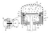
- FIGS. 1A and 1Bare schematic views to explain an apparatus for CVD according to the present invention.
- FIGS. 1A and 1Bare schematic views to explain an apparatus for CVD according to the present invention.
- the reaction chamber 10is a single type chamber in which wafers are inserted one by one, and an upper portion thereof is formed as a quartz dome 20 .
- a bell jar 30 for covering the quartz dome 20is installed at an outer portion of the quartz dome 20 .
- the bell jar 30is provided with a bell jar heater 40 at an inner portion thereof.
- a wafer supporting member 50is installed at an inner portion of the reaction chamber 10 , and a wafer 60 is located on the wafer supporting member 50 .
- the wafer supporting member 50is provided with a main heater (not shown) for heating the wafer 60 with a proper temperature in which a chemical vapor deposition is performed.
- the wafer supporting member 50is supported by a supporting axis.
- the supporting axis 52is surrounded by bellows 55 , so that a hermetic state is maintained between outside and inside of the reaction chamber 10 even if the supporting axis is transported up and down by the bellows 55 .
- a gas focus ring 70is installed at an inner side portion of the reaction chamber 10 so as to surround a lateral portion of the wafer supporting member 50 .
- the gas focus ring 70is provided with a plurality of injection holes 72 . Injection rings can replace the ejection holes 72 .
- a purge gas supplying hole 90 for supplying purge gas such as N 2 or Ar into the reaction chamber 10is installed at a lower surface of the reaction chamber 10 .
- a gas outlet 80 for exhausting processing gas injected through the gas focus ring 70 and purge gas supplied through the purge gas supplying hole 90is installed at a lateral surface of the reaction chamber 10 .
- the gas outlet 80is located below the gas focus ring 70 and has a recess formed as a ring shape along an inner surface of the reaction chamber.
- the gas outlet 80is preferably installed at the same height as the wafer supporting member 50 .
- the gas outlet 80is connected to one vacuum pump (not shown) by a pumping line 82 .
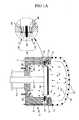
- a shielding layer 85 for preventing the processing gas and the purge gas from being mixed each other at the gas outlet 80is horizontally installed at a middle portion of the gas outlet 80 . Accordingly, the gas outlet 80 is divided into a lower gas outlet 88 and an upper gas outlet 87 . The purge gas injected through the purge gas supplying hole 90 is exhausted through the lower gas outlet 88 , and the processing gas injected through the gas focus ring is exhausted through the upper gas outlet 87 .
- the gas outlet 80is divided into upper and lower spaces by the shielding layer 85 , which is not completely divided, but the upper and lower spaces are put together at an end portion of the shielding layer 85 .
- the processing gas and the purge gas introduced to the gas outlet 80is exhausted outwardly through the pumping line 82 .
- the lower gas outlet 88is divided into three spaces 88 a , 88 b , and 88 c by a horizontal division of two lower division layers 84 .
- the lower division layer 84has a large inner diameter than the shielding layer 85 .
- the spaces 88 a , 88 b , and 88 chave higher heights towards an upper direction. If the lower gas outlet 88 is not divided, the purge gas is introduced at the space at one time, thereby generating turbulence. However, if the lower gas outlet 88 is divided into 88 a , 88 b , and 88 c , the purge gas is sequentially exhausted from a lower space little by little, thereby not causing the turbulence.
- the upper gas outlet 87is divided into three spaces 87 a , 87 b , and 87 c by a horizontal division of two upper division layers 86 .
- the spaces 87 a , 87 b , and 87 chas higher heights towards a lower direction.
- the upper division layer 87has a large inner diameter than the shielding layer 85 .
- the processing gasis injected to the gas focus ring 70 through the gas supplying line 74 , the processing gas is injected from a peripheral portion of the wafer supporting member 50 to an upper center portion of the wafer supporting member 50 through the injection holes 72 .
- the processing gas injected to the upper center portion of the wafer supporting member 50collides to the quartz dome 20 being heated by the bell jar heater 40 and is decomposed thermally, thereby uniformly being distributed to an upper space of the wafer supporting member 50 . Accordingly, even if the wafer 60 has a large diameter, a uniform chemical vapor deposition takes place at a whole surface of the wafer 60 .
- Residual processing gas which does not contribute to the CVDis exhausted outwardly through the gas outlet 80 .
- the purge gasis supplied with a proper flow rate through the purge gas supplying hole 90 .
- the purge gasshould be also prevented from mounting to an upper portion of the reaction chamber 10 by a pressure of the processing gas.
- the processing gasdoes not come down to a lower space of the wafer supporting member 50 by a supply of the purge gas, so that a thin film is prevented from being deposited at an inner wall of a lower portion of the reaction chamber 10 such as the wafer supporting member 50 and the supporting axis 52 .
- the purge gasis also prevented from mounting to an upper space of the wafer supporting member 50 , thereby not influencing to the CVD. According to this, a uniformity and a deposition speed of a thin film are not influenced by the purge gas. The said effects are more remarkably shown by installing the shielding layer 85 .
- the processing gasis prevented from coming down to a lower space of the reaction chamber 10 by a pressure of the purge gas, thereby preventing the processing gas from being deposited to a lower space of the reaction chamber 10 . Accordingly, not only a particle source is minimized, but also a period to check an equipment can be prolonged. Also, the purge gas is also prevented from mounting to an upper space of the reaction chamber 10 by a pressure of the processing gas, so that the CVD process is hardly influenced by the purge gas.
- turbulence by a mixture between the processing gas and the purge gasis prevented by installing the shielding layer 85 and thereby having two entrances in the gas outlet. If the turbulence is generated at the gas outlet 80 , in case of that gas is stagnant, heat from the main heater installed at the wafer supporting member 50 causes a burning phenomenon. Also, the processing gas and the purge gas is respectively exhausted from spaces formed by the upper division layers 86 and the lower division layers 84 little by little, thereby more decreasing the turbulence. An amount of exhaustion becomes more toward the shielding layer 80 .
Landscapes
- Chemical & Material Sciences (AREA)
- General Chemical & Material Sciences (AREA)
- Chemical Kinetics & Catalysis (AREA)
- Engineering & Computer Science (AREA)
- Materials Engineering (AREA)
- Mechanical Engineering (AREA)
- Metallurgy (AREA)
- Organic Chemistry (AREA)
- Chemical Vapour Deposition (AREA)
Abstract
Description
- 1. Field of the Invention[0001]
- The present invention relates to an apparatus for chemical vapor deposition (CVD), and more particularly, to an apparatus for CVD which can prevent a thin layer unexpectedly deposited in a lower space of a reaction chamber from working as a particle source.[0002]
- 2. Description of the Background Art[0003]
- In an apparatus for CVD in accordance with the conventional art, a gas outlet is generally installed at a lower surface of a reaction chamber. Accordingly, when gas which does not contribute to a thin layer deposition is exhausted outwardly through the gas outlet, the gas is deposited at the lower space of the reaction chamber, so that the lower space works as a particle generating source.[0004]
- Therefore, an object of the present invention is to provide an apparatus for CVD which can prolong a period to check an equipment by removing a particle source by preventing gas which does not contribute to a thin layer deposition from going down to a lower space of a reaction chamber.[0005]
- To achieve these and other advantages and in accordance with the purpose of the present invention, as embodied and broadly described herein, there is provided an apparatus for CVD comprising a reaction chamber for performing a chemical vapor deposition; a wafer supporting member installed in the reaction chamber for mounting a wafer; a gas focus ring installed at an inner surface of the reaction chamber for injecting processing gas from a peripheral portion of the wafer supporting member to an upper center portion of the wafer supporting member; a purge gas supplying hole installed at a lower surface of the reaction chamber for supplying purge gas to an inner portion of the reaction chamber; a ring-shaped gas outlet parallel to a lateral wall of the reaction chamber and located below the gas focus ring for exhausting processing gas injected through the gas focus ring and purge gas supplied through the purge gas supplying hole; one pumping line for connecting the gas outlet and a vacuum pump each other; a shielding layer parallel to the gas outlet and located at a middle portion of the gas outlet for preventing the processing gas and the purge gas exhausted through the gas outlet from being mixed at an entrance of the gas outlet; a plurality of lower division layers with a larger inner diameter than the shielding layer for horizontally dividing the gas outlet below the shielding layer into a plurality of spaces; and a plurality of upper division layers with a larger inner diameter than the shielding layer for horizontally dividing the gas outlet above the shielding layer into a plurality of spaces.[0006]
- The foregoing and other objects, features, aspects and advantages of the present invention will become more apparent from the following detailed description of the present invention when taken in conjunction with the accompanying drawings.[0007]
- The accompanying drawings, which are included to provide a further understanding of the invention and are incorporated in and constitute a part of this specification, illustrate embodiments of the invention and together with the description serve to explain the principles of the invention.[0008]
- In the drawings:[0009]
- FIGS. 1A and 1B are schematic views to explain an apparatus for CVD according to the present invention.[0010]
- Reference will now be made in detail to the preferred embodiments of the present invention, examples of which are illustrated in the accompanying drawings.[0011]
- Hereinafter, preferred embodiments of the present invention will be explained with reference to attached drawings.[0012]
- FIGS. 1A and 1B are schematic views to explain an apparatus for CVD according to the present invention.[0013]
- Referring to FIGS. 1A and 1B, the[0014]
reaction chamber 10 is a single type chamber in which wafers are inserted one by one, and an upper portion thereof is formed as aquartz dome 20. Abell jar 30 for covering thequartz dome 20 is installed at an outer portion of thequartz dome 20. Thebell jar 30 is provided with abell jar heater 40 at an inner portion thereof. Awafer supporting member 50 is installed at an inner portion of thereaction chamber 10, and a wafer60 is located on thewafer supporting member 50. Thewafer supporting member 50 is provided with a main heater (not shown) for heating the wafer60 with a proper temperature in which a chemical vapor deposition is performed. Thewafer supporting member 50 is supported by a supporting axis. The supportingaxis 52 is surrounded bybellows 55, so that a hermetic state is maintained between outside and inside of thereaction chamber 10 even if the supporting axis is transported up and down by thebellows 55. - A[0015]
gas focus ring 70 is installed at an inner side portion of thereaction chamber 10 so as to surround a lateral portion of thewafer supporting member 50. Thegas focus ring 70 is provided with a plurality ofinjection holes 72. Injection rings can replace theejection holes 72. - A purge[0016]
gas supplying hole 90 for supplying purge gas such as N2or Ar into thereaction chamber 10 is installed at a lower surface of thereaction chamber 10. - A[0017]
gas outlet 80 for exhausting processing gas injected through thegas focus ring 70 and purge gas supplied through the purgegas supplying hole 90 is installed at a lateral surface of thereaction chamber 10. Thegas outlet 80 is located below thegas focus ring 70 and has a recess formed as a ring shape along an inner surface of the reaction chamber. Thegas outlet 80 is preferably installed at the same height as thewafer supporting member 50. Thegas outlet 80 is connected to one vacuum pump (not shown) by apumping line 82. - A[0018]
shielding layer 85 for preventing the processing gas and the purge gas from being mixed each other at thegas outlet 80 is horizontally installed at a middle portion of thegas outlet 80. Accordingly, thegas outlet 80 is divided into alower gas outlet 88 and anupper gas outlet 87. The purge gas injected through the purgegas supplying hole 90 is exhausted through thelower gas outlet 88, and the processing gas injected through the gas focus ring is exhausted through theupper gas outlet 87. - The[0019]
gas outlet 80 is divided into upper and lower spaces by theshielding layer 85, which is not completely divided, but the upper and lower spaces are put together at an end portion of theshielding layer 85. The processing gas and the purge gas introduced to thegas outlet 80 is exhausted outwardly through thepumping line 82. - The[0020]
lower gas outlet 88 is divided into threespaces lower division layers 84. Thelower division layer 84 has a large inner diameter than theshielding layer 85. Thespaces lower gas outlet 88 is not divided, the purge gas is introduced at the space at one time, thereby generating turbulence. However, if thelower gas outlet 88 is divided into88a,88b, and88c, the purge gas is sequentially exhausted from a lower space little by little, thereby not causing the turbulence. Theupper gas outlet 87 is divided into threespaces upper division layers 86. Thespaces upper division layer 87 has a large inner diameter than theshielding layer 85. - If the processing gas is injected to the[0021]
gas focus ring 70 through thegas supplying line 74, the processing gas is injected from a peripheral portion of thewafer supporting member 50 to an upper center portion of thewafer supporting member 50 through theinjection holes 72. The processing gas injected to the upper center portion of thewafer supporting member 50 collides to thequartz dome 20 being heated by thebell jar heater 40 and is decomposed thermally, thereby uniformly being distributed to an upper space of thewafer supporting member 50. Accordingly, even if the wafer60 has a large diameter, a uniform chemical vapor deposition takes place at a whole surface of the wafer60. - Residual processing gas which does not contribute to the CVD is exhausted outwardly through the[0022]
gas outlet 80. At this time, the purge gas is supplied with a proper flow rate through the purgegas supplying hole 90. The purge gas should be also prevented from mounting to an upper portion of thereaction chamber 10 by a pressure of the processing gas. - The processing gas does not come down to a lower space of the[0023]
wafer supporting member 50 by a supply of the purge gas, so that a thin film is prevented from being deposited at an inner wall of a lower portion of thereaction chamber 10 such as thewafer supporting member 50 and the supportingaxis 52. The purge gas is also prevented from mounting to an upper space of thewafer supporting member 50, thereby not influencing to the CVD. According to this, a uniformity and a deposition speed of a thin film are not influenced by the purge gas. The said effects are more remarkably shown by installing theshielding layer 85. - As aforementioned, according to the apparatus of CVD of the present invention, the processing gas is prevented from coming down to a lower space of the[0024]
reaction chamber 10 by a pressure of the purge gas, thereby preventing the processing gas from being deposited to a lower space of thereaction chamber 10. Accordingly, not only a particle source is minimized, but also a period to check an equipment can be prolonged. Also, the purge gas is also prevented from mounting to an upper space of thereaction chamber 10 by a pressure of the processing gas, so that the CVD process is hardly influenced by the purge gas. - Also, turbulence by a mixture between the processing gas and the purge gas is prevented by installing the[0025]
shielding layer 85 and thereby having two entrances in the gas outlet. If the turbulence is generated at thegas outlet 80, in case of that gas is stagnant, heat from the main heater installed at thewafer supporting member 50 causes a burning phenomenon. Also, the processing gas and the purge gas is respectively exhausted from spaces formed by the upper division layers86 and the lower division layers84 little by little, thereby more decreasing the turbulence. An amount of exhaustion becomes more toward theshielding layer 80. - As the present invention may be embodied in several forms without departing from the spirit or essential characteristics thereof, it should also be understood that the above-described embodiments are not limited by any of the details of the foregoing description, unless otherwise specified, but rather should be construed broadly within its spirit and scope as defined in the appended claims, and therefore all changes and modifications that fall within the metes and bounds of the claims, or equivalence of such metes and bounds are therefore intended to be embraced by the appended claims.[0026]
Claims (7)
Applications Claiming Priority (4)
| Application Number | Priority Date | Filing Date | Title |
|---|---|---|---|
| KR10-2001-0068511AKR100443598B1 (en) | 2001-11-05 | 2001-11-05 | Apparatus for Chemical Vapor Deposition |
| KR68511/2001 | 2001-11-05 | ||
| KR73336/2001 | 2001-11-23 | ||
| KR10-2001-0073336AKR100445814B1 (en) | 2001-11-23 | 2001-11-23 | Apparatus for Chemical Vapor Deposition |
Publications (2)
| Publication Number | Publication Date |
|---|---|
| US20030084849A1true US20030084849A1 (en) | 2003-05-08 |
| US7390366B2 US7390366B2 (en) | 2008-06-24 |
Family
ID=26639442
Family Applications (1)
| Application Number | Title | Priority Date | Filing Date |
|---|---|---|---|
| US10/282,304Expired - LifetimeUS7390366B2 (en) | 2001-11-05 | 2002-10-28 | Apparatus for chemical vapor deposition |
Country Status (2)
| Country | Link |
|---|---|
| US (1) | US7390366B2 (en) |
| JP (1) | JP4078185B2 (en) |
Cited By (10)
| Publication number | Priority date | Publication date | Assignee | Title |
|---|---|---|---|---|
| US20040040940A1 (en)* | 2002-08-28 | 2004-03-04 | Tokyo Electron Limited | Asymmetrical focus ring |
| US7552521B2 (en) | 2004-12-08 | 2009-06-30 | Tokyo Electron Limited | Method and apparatus for improved baffle plate |
| US20090165713A1 (en)* | 2007-12-26 | 2009-07-02 | Samsung Electro-Mechanics Co, Ltd. | Chemical vapor deposition apparatus |
| US7601242B2 (en) | 2005-01-11 | 2009-10-13 | Tokyo Electron Limited | Plasma processing system and baffle assembly for use in plasma processing system |
| US20090260572A1 (en)* | 2008-04-18 | 2009-10-22 | Samsung Electro-Mechanics Co., Ltd. | Chemical vapor deposition apparatus |
| US20090260569A1 (en)* | 2008-04-18 | 2009-10-22 | Samsung Electro-Mechanics Co., Ltd. | Chemical vapor deposition apparatus |
| US20100154996A1 (en)* | 2008-12-19 | 2010-06-24 | Eric Hudson | Plasma confinement structures in plasma processing systems |
| US20110229638A1 (en)* | 2010-03-19 | 2011-09-22 | Gt Solar Incorporated | System and method for polycrystalline silicon deposition |
| TWI410520B (en)* | 2007-12-26 | 2013-10-01 | Samsung Electronics Co Ltd | Chemical vapor deposition apparatus |
| CN112992743A (en)* | 2021-05-17 | 2021-06-18 | 北京北方华创微电子装备有限公司 | Semiconductor process chamber and semiconductor process equipment |
Families Citing this family (14)
| Publication number | Priority date | Publication date | Assignee | Title |
|---|---|---|---|---|
| JP5004513B2 (en)* | 2006-06-09 | 2012-08-22 | Sumco Techxiv株式会社 | Vapor growth apparatus and vapor growth method |
| US8707899B2 (en)* | 2009-02-26 | 2014-04-29 | Hitachi High-Technologies Corporation | Plasma processing apparatus |
| US8968473B2 (en)* | 2009-09-21 | 2015-03-03 | Silevo, Inc. | Stackable multi-port gas nozzles |
| US9441295B2 (en) | 2010-05-14 | 2016-09-13 | Solarcity Corporation | Multi-channel gas-delivery system |
| US9240513B2 (en) | 2010-05-14 | 2016-01-19 | Solarcity Corporation | Dynamic support system for quartz process chamber |
| KR102217790B1 (en)* | 2012-09-26 | 2021-02-18 | 어플라이드 머티어리얼스, 인코포레이티드 | An apparatus and method for purging gaseous compounds |
| JP2017518626A (en) | 2015-02-17 | 2017-07-06 | ソーラーシティ コーポレーション | Method and system for improving manufacturing yield of solar cells |
| US20160359080A1 (en) | 2015-06-07 | 2016-12-08 | Solarcity Corporation | System, method and apparatus for chemical vapor deposition |
| US9748434B1 (en) | 2016-05-24 | 2017-08-29 | Tesla, Inc. | Systems, method and apparatus for curing conductive paste |
| JP6756853B2 (en)* | 2016-06-03 | 2020-09-16 | アプライド マテリアルズ インコーポレイテッドApplied Materials,Incorporated | Effective and new design for low particle count and better wafer quality by diffusing the flow inside the chamber |
| US9954136B2 (en) | 2016-08-03 | 2018-04-24 | Tesla, Inc. | Cassette optimized for an inline annealing system |
| US10115856B2 (en) | 2016-10-31 | 2018-10-30 | Tesla, Inc. | System and method for curing conductive paste using induction heating |
| JP7477515B2 (en)* | 2019-01-08 | 2024-05-01 | アプライド マテリアルズ インコーポレイテッド | Pumping apparatus and method for a substrate processing chamber - Patents.com |
| CN112951697B (en)* | 2019-11-26 | 2025-07-29 | Asmip私人控股有限公司 | Substrate processing apparatus |
Citations (7)
| Publication number | Priority date | Publication date | Assignee | Title |
|---|---|---|---|---|
| US4545327A (en)* | 1982-08-27 | 1985-10-08 | Anicon, Inc. | Chemical vapor deposition apparatus |
| US5338363A (en)* | 1991-12-13 | 1994-08-16 | Mitsubishi Denki Kabushiki Kaisha | Chemical vapor deposition method, and chemical vapor deposition treatment system and chemical vapor deposition apparatus therefor |
| US5592581A (en)* | 1993-07-19 | 1997-01-07 | Tokyo Electron Kabushiki Kaisha | Heat treatment apparatus |
| US5928426A (en)* | 1996-08-08 | 1999-07-27 | Novellus Systems, Inc. | Method and apparatus for treating exhaust gases from CVD, PECVD or plasma etch reactors |
| US5972116A (en)* | 1994-12-29 | 1999-10-26 | F.T.I. Co., Ltd. | Method and apparatus for producing a semiconductor device |
| US5997651A (en)* | 1995-10-18 | 1999-12-07 | Tokyo Electron Limited | Heat treatment apparatus |
| US6223684B1 (en)* | 1997-07-07 | 2001-05-01 | Canon Kabushiki Kaisha | Film deposition apparatus |
Family Cites Families (1)
| Publication number | Priority date | Publication date | Assignee | Title |
|---|---|---|---|---|
| JPH05175130A (en) | 1991-12-20 | 1993-07-13 | Nippon Steel Corp | Plasma cvd apparatus |
- 2002
- 2002-10-28USUS10/282,304patent/US7390366B2/ennot_activeExpired - Lifetime
- 2002-10-30JPJP2002316228Apatent/JP4078185B2/ennot_activeExpired - Fee Related
Patent Citations (7)
| Publication number | Priority date | Publication date | Assignee | Title |
|---|---|---|---|---|
| US4545327A (en)* | 1982-08-27 | 1985-10-08 | Anicon, Inc. | Chemical vapor deposition apparatus |
| US5338363A (en)* | 1991-12-13 | 1994-08-16 | Mitsubishi Denki Kabushiki Kaisha | Chemical vapor deposition method, and chemical vapor deposition treatment system and chemical vapor deposition apparatus therefor |
| US5592581A (en)* | 1993-07-19 | 1997-01-07 | Tokyo Electron Kabushiki Kaisha | Heat treatment apparatus |
| US5972116A (en)* | 1994-12-29 | 1999-10-26 | F.T.I. Co., Ltd. | Method and apparatus for producing a semiconductor device |
| US5997651A (en)* | 1995-10-18 | 1999-12-07 | Tokyo Electron Limited | Heat treatment apparatus |
| US5928426A (en)* | 1996-08-08 | 1999-07-27 | Novellus Systems, Inc. | Method and apparatus for treating exhaust gases from CVD, PECVD or plasma etch reactors |
| US6223684B1 (en)* | 1997-07-07 | 2001-05-01 | Canon Kabushiki Kaisha | Film deposition apparatus |
Cited By (17)
| Publication number | Priority date | Publication date | Assignee | Title |
|---|---|---|---|---|
| US6963043B2 (en)* | 2002-08-28 | 2005-11-08 | Tokyo Electron Limited | Asymmetrical focus ring |
| US20040040940A1 (en)* | 2002-08-28 | 2004-03-04 | Tokyo Electron Limited | Asymmetrical focus ring |
| US7552521B2 (en) | 2004-12-08 | 2009-06-30 | Tokyo Electron Limited | Method and apparatus for improved baffle plate |
| US7601242B2 (en) | 2005-01-11 | 2009-10-13 | Tokyo Electron Limited | Plasma processing system and baffle assembly for use in plasma processing system |
| US20090165713A1 (en)* | 2007-12-26 | 2009-07-02 | Samsung Electro-Mechanics Co, Ltd. | Chemical vapor deposition apparatus |
| TWI410520B (en)* | 2007-12-26 | 2013-10-01 | Samsung Electronics Co Ltd | Chemical vapor deposition apparatus |
| US8298338B2 (en)* | 2007-12-26 | 2012-10-30 | Samsung Electronics Co., Ltd. | Chemical vapor deposition apparatus |
| US8277561B2 (en) | 2008-04-18 | 2012-10-02 | Samsung Electronics Co., Ltd. | Chemical vapor deposition apparatus |
| US20090260572A1 (en)* | 2008-04-18 | 2009-10-22 | Samsung Electro-Mechanics Co., Ltd. | Chemical vapor deposition apparatus |
| US20090260569A1 (en)* | 2008-04-18 | 2009-10-22 | Samsung Electro-Mechanics Co., Ltd. | Chemical vapor deposition apparatus |
| US8540844B2 (en)* | 2008-12-19 | 2013-09-24 | Lam Research Corporation | Plasma confinement structures in plasma processing systems |
| US20100154996A1 (en)* | 2008-12-19 | 2010-06-24 | Eric Hudson | Plasma confinement structures in plasma processing systems |
| US20140007413A1 (en)* | 2008-12-19 | 2014-01-09 | Eric Hudson | Plasma confinement structures in plasma processing systems and methods thereof |
| US8677590B2 (en)* | 2008-12-19 | 2014-03-25 | Lam Research Corporation | Plasma confinement structures in plasma processing systems and methods thereof |
| WO2011116273A3 (en)* | 2010-03-19 | 2012-01-19 | Gt Solar Incorporated | System and method for polycrystalline silicon deposition |
| US20110229638A1 (en)* | 2010-03-19 | 2011-09-22 | Gt Solar Incorporated | System and method for polycrystalline silicon deposition |
| CN112992743A (en)* | 2021-05-17 | 2021-06-18 | 北京北方华创微电子装备有限公司 | Semiconductor process chamber and semiconductor process equipment |
Also Published As
| Publication number | Publication date |
|---|---|
| US7390366B2 (en) | 2008-06-24 |
| JP4078185B2 (en) | 2008-04-23 |
| JP2003277936A (en) | 2003-10-02 |
Similar Documents
| Publication | Publication Date | Title |
|---|---|---|
| US7390366B2 (en) | Apparatus for chemical vapor deposition | |
| US6383954B1 (en) | Process gas distribution for forming stable fluorine-doped silicate glass and other films | |
| KR100862658B1 (en) | Gas injection device of semiconductor processing system | |
| TWI722871B (en) | Lid and lid assembly kit for substrate processing chamber | |
| US5232508A (en) | Gaseous phase chemical treatment reactor | |
| US6085690A (en) | Chemical vapor deposition apparatus | |
| US6435428B2 (en) | Showerhead apparatus for radical-assisted deposition | |
| US7510624B2 (en) | Self-cooling gas delivery apparatus under high vacuum for high density plasma applications | |
| US20090034147A1 (en) | Method and apparatus for providing an electrostatic chuck with reduced plasma penetration and arcing | |
| KR19980033001A (en) | Faceplate Heat Chokes in Chemical Vapor Deposition Reactors | |
| WO2008094752A1 (en) | Processing chamber with heated chamber liner | |
| KR20160108176A (en) | Method and apparatus to minimize seam effect during teos oxide film deposition | |
| KR20010078110A (en) | Method and apparatus for cleaning a semiconductor wafer processing system, and a computer-readable medium to control the system | |
| KR100453014B1 (en) | Apparatus for Chemical Vapor Deposition | |
| US6435197B2 (en) | Method of cleaning a semiconductor fabricating apparatus | |
| KR101345112B1 (en) | Thin film deposition apparatus | |
| KR100484945B1 (en) | Semiconductor device fabrication apparatus having multi-hole angled gas injection system | |
| US20030015291A1 (en) | Semiconductor device fabrication apparatus having multi-hole angled gas injection system | |
| KR101108579B1 (en) | Furnace Semiconductor Equipment | |
| KR100445814B1 (en) | Apparatus for Chemical Vapor Deposition | |
| KR100697267B1 (en) | Chemical Vapor Deposition Equipment | |
| KR100581860B1 (en) | Thin film deposition equipment | |
| KR100443598B1 (en) | Apparatus for Chemical Vapor Deposition | |
| KR102308115B1 (en) | Substrate processing apparatus | |
| KR20220116519A (en) | Asymmetric purged block below wafer plane to manage non-uniformity |
Legal Events
| Date | Code | Title | Description |
|---|---|---|---|
| AS | Assignment | Owner name:JUSUNG ENGINEERING CO., LTD., KOREA, REPUBLIC OF Free format text:ASSIGNMENT OF ASSIGNORS INTEREST;ASSIGNOR:SHIM, KYUNG-SIK;REEL/FRAME:013433/0154 Effective date:20021008 | |
| STCF | Information on status: patent grant | Free format text:PATENTED CASE | |
| FEPP | Fee payment procedure | Free format text:PAT HOLDER NO LONGER CLAIMS SMALL ENTITY STATUS, ENTITY STATUS SET TO UNDISCOUNTED (ORIGINAL EVENT CODE: STOL); ENTITY STATUS OF PATENT OWNER: SMALL ENTITY | |
| FEPP | Fee payment procedure | Free format text:PAYOR NUMBER ASSIGNED (ORIGINAL EVENT CODE: ASPN); ENTITY STATUS OF PATENT OWNER: SMALL ENTITY | |
| FEPP | Fee payment procedure | Free format text:PAYER NUMBER DE-ASSIGNED (ORIGINAL EVENT CODE: RMPN); ENTITY STATUS OF PATENT OWNER: SMALL ENTITY Free format text:PAYOR NUMBER ASSIGNED (ORIGINAL EVENT CODE: ASPN); ENTITY STATUS OF PATENT OWNER: SMALL ENTITY | |
| FPAY | Fee payment | Year of fee payment:4 | |
| FEPP | Fee payment procedure | Free format text:PAT HOLDER CLAIMS SMALL ENTITY STATUS, ENTITY STATUS SET TO SMALL (ORIGINAL EVENT CODE: LTOS); ENTITY STATUS OF PATENT OWNER: SMALL ENTITY | |
| FPAY | Fee payment | Year of fee payment:8 | |
| MAFP | Maintenance fee payment | Free format text:PAYMENT OF MAINTENANCE FEE, 12TH YR, SMALL ENTITY (ORIGINAL EVENT CODE: M2553); ENTITY STATUS OF PATENT OWNER: SMALL ENTITY Year of fee payment:12 |