US20030081095A1 - Printing system and method for fabricating a liquid crystal display device - Google Patents
Printing system and method for fabricating a liquid crystal display deviceDownload PDFInfo
- Publication number
- US20030081095A1 US20030081095A1US10/183,480US18348002AUS2003081095A1US 20030081095 A1US20030081095 A1US 20030081095A1US 18348002 AUS18348002 AUS 18348002AUS 2003081095 A1US2003081095 A1US 2003081095A1
- Authority
- US
- United States
- Prior art keywords
- cliché
- clean chamber
- substrate
- interior
- grooves
- Prior art date
- Legal status (The legal status is an assumption and is not a legal conclusion. Google has not performed a legal analysis and makes no representation as to the accuracy of the status listed.)
- Granted
Links
Images


Classifications
- G—PHYSICS
- G02—OPTICS
- G02F—OPTICAL DEVICES OR ARRANGEMENTS FOR THE CONTROL OF LIGHT BY MODIFICATION OF THE OPTICAL PROPERTIES OF THE MEDIA OF THE ELEMENTS INVOLVED THEREIN; NON-LINEAR OPTICS; FREQUENCY-CHANGING OF LIGHT; OPTICAL LOGIC ELEMENTS; OPTICAL ANALOGUE/DIGITAL CONVERTERS
- G02F1/00—Devices or arrangements for the control of the intensity, colour, phase, polarisation or direction of light arriving from an independent light source, e.g. switching, gating or modulating; Non-linear optics
- G02F1/01—Devices or arrangements for the control of the intensity, colour, phase, polarisation or direction of light arriving from an independent light source, e.g. switching, gating or modulating; Non-linear optics for the control of the intensity, phase, polarisation or colour
- G02F1/13—Devices or arrangements for the control of the intensity, colour, phase, polarisation or direction of light arriving from an independent light source, e.g. switching, gating or modulating; Non-linear optics for the control of the intensity, phase, polarisation or colour based on liquid crystals, e.g. single liquid crystal display cells
- B—PERFORMING OPERATIONS; TRANSPORTING
- B41—PRINTING; LINING MACHINES; TYPEWRITERS; STAMPS
- B41J—TYPEWRITERS; SELECTIVE PRINTING MECHANISMS, i.e. MECHANISMS PRINTING OTHERWISE THAN FROM A FORME; CORRECTION OF TYPOGRAPHICAL ERRORS
- B41J2/00—Typewriters or selective printing mechanisms characterised by the printing or marking process for which they are designed
- B41J2/005—Typewriters or selective printing mechanisms characterised by the printing or marking process for which they are designed characterised by bringing liquid or particles selectively into contact with a printing material
- B41J2/01—Ink jet
- G—PHYSICS
- G02—OPTICS
- G02B—OPTICAL ELEMENTS, SYSTEMS OR APPARATUS
- G02B5/00—Optical elements other than lenses
- G02B5/20—Filters
- G02B5/201—Filters in the form of arrays
- B—PERFORMING OPERATIONS; TRANSPORTING
- B41—PRINTING; LINING MACHINES; TYPEWRITERS; STAMPS
- B41J—TYPEWRITERS; SELECTIVE PRINTING MECHANISMS, i.e. MECHANISMS PRINTING OTHERWISE THAN FROM A FORME; CORRECTION OF TYPOGRAPHICAL ERRORS
- B41J2202/00—Embodiments of or processes related to ink-jet or thermal heads
- B41J2202/01—Embodiments of or processes related to ink-jet heads
- B41J2202/09—Ink jet technology used for manufacturing optical filters
- G—PHYSICS
- G02—OPTICS
- G02F—OPTICAL DEVICES OR ARRANGEMENTS FOR THE CONTROL OF LIGHT BY MODIFICATION OF THE OPTICAL PROPERTIES OF THE MEDIA OF THE ELEMENTS INVOLVED THEREIN; NON-LINEAR OPTICS; FREQUENCY-CHANGING OF LIGHT; OPTICAL LOGIC ELEMENTS; OPTICAL ANALOGUE/DIGITAL CONVERTERS
- G02F1/00—Devices or arrangements for the control of the intensity, colour, phase, polarisation or direction of light arriving from an independent light source, e.g. switching, gating or modulating; Non-linear optics
- G02F1/01—Devices or arrangements for the control of the intensity, colour, phase, polarisation or direction of light arriving from an independent light source, e.g. switching, gating or modulating; Non-linear optics for the control of the intensity, phase, polarisation or colour
- G02F1/13—Devices or arrangements for the control of the intensity, colour, phase, polarisation or direction of light arriving from an independent light source, e.g. switching, gating or modulating; Non-linear optics for the control of the intensity, phase, polarisation or colour based on liquid crystals, e.g. single liquid crystal display cells
- G02F1/133—Constructional arrangements; Operation of liquid crystal cells; Circuit arrangements
- G02F1/1333—Constructional arrangements; Manufacturing methods
- G02F1/1335—Structural association of cells with optical devices, e.g. polarisers or reflectors
- G02F1/133509—Filters, e.g. light shielding masks
- G02F1/133514—Colour filters
- G02F1/133516—Methods for their manufacture, e.g. printing, electro-deposition or photolithography
Definitions
- the present inventionrelates to a printing system and method used for fabricating a liquid crystal display device, and more particularly, to a printing system and printing method for fabricating a thin film transistor, a color filter, and a black matrix of a liquid crystal display device
- cathode ray tube (CRT) monitorsare commonly used to display information on a computer displays and televisions because of the CRT monitor's superior picture quality and image brightness.
- CRT monitorsAs demand for larger displays increases, the size of the CRT monitors also increases. Accordingly, the overall size of the CRT monitor eventually increases to a point where it's size is too large to efficiently display image data.
- mobility of the CRT monitordecreases as overall weight of the CRT monitor increases.
- LCDliquid crystal display
- PDPplasma display panel
- ELorganic electro luminescence
- LEDslight emitting diodes
- field emission displayshave gained in popularity.
- LCDliquid crystal display
- FIG. 1is a cross-sectional view of an LCD device panel according to the conventional art.
- the LCD device panelis formed of a lower substrate and an upper substrate.
- the upper substrateincludes a glass substrate 10 having a color filter layer 11 , a black matrix 12 , an orientation layer 14 , and a common electrode 13 .
- Both the black matrix 12 and the color filter layer 11are formed on the glass substrate 10 , wherein the black matrix 12 is disposed between adjacent color filter layers 11 .
- the color filter layer 11includes a resin film containing dye or three basic colors of red, green, and blue or a pigment thereof.
- An overcoat film(not shown) is provided for smoothing the color filter layer 11 and improving an adhesive force with the common electrode 13 , which is commonly formed of a transparent conductive material, such as indium tin oxide (ITO).
- ITOindium tin oxide
- the orientation layer 14aligns a liquid crystal material formed between the upper and lower substrates.
- the lower substrateincludes a glass substrate 10 having a thin film transistor (TFT) formed thereon, a protection film 20 , a pixel electrode 21 , and an orientation layer 14
- the TFTincludes a gate electrode 15 , an active layer 16 , a source electrode 18 , and a drain electrode 19 .
- the gate electrode 15is formed on the glass substrate 10 with a gate insulating layer 17 formed on the gate electrode 15 and the glass substrate 10 .
- the active layer 16includes a semiconductor layer 16 a formed by depositing an amorphous silicon (a-Si) and a n+doped ohmic contact layer 16 b at opposing upper portions of the semiconductor layer 16 a .
- the protection film 20is formed to cover the TFT and the gate insulating film 17 .
- the pixel electrode 21is formed on the protection film 20 and is formed of a transparent conductive material, such ITO
- the orientation layer 14is formed on the pixel electrode 21 and the protection film 20 .
- Polarizing films 22are disposed on the outside surfaces of the upper and lower substrate respectively
- light transmittance through the liquid crystal layer formed between the upper and lower substratesis controlled by application of an electric potential on the common electrode 13 and the pixel electrode 21 .
- the common electrode 13commonly receives a constant potential
- the pixel electrode 21receives a data signal to generate the electric field.
- the pixel electrode 21receives the data signal when the TFT is turned on. Specifically, a data signal is supplied to the source electrode 18 of the TFT and is transmitted via the active layer 16 a through the ohmic contact layer 16 b when the gate electrode 15 is enabled by receiving a scan signal. Accordingly, the data signal is transmitted to the drain electrode 19 and applied to the pixel electrode 21 , thereby generating the electric field in combination with the common electrode 13 and controlling the light transmitted through the liquid crystal layer.
- Fabrication of the LCD devicecommonly includes a thin film deposition process, a photolithographic process, and an etching process that are repeatedly performed.
- fabrication of the TFT, the color filter layer 11 , and the black matrix 12includes sequential printing processes of ink or photoresist materials.
- the printing processesinclude a gravure offset method and a transfer method depending upon how the photoresist material is applied to the upper mid lower substrates.
- the gravure offset methodincludes steps of filling the photoresist material into a groove of a cliché, transferring the photoresist material filled in the groove onto a roller; and applying the transferred photoresist material onto the upper or lower substrate.
- FIGS. 2A to 2 Dare cross-sectional views of a sequential printing process according to a gravure offset printing method according to the conventional art.
- a photoresist or ink material 29is filled into a plurality of rectangular grooves 26 formed in a surface of a cliché, wherein the plurality of rectangular grooves are spaced apart to define a pattern
- any excess photoresist material 29 that remains on the surface of the clichéis removed by a doctor blade 27 . Accordingly, the photoresist material 29 only remains in each of the plurality of rectangular grooves 26
- a roller 25is rolled across the surface of the cliché along a first direction so that individual photoresist material portions 24 of the photoresist material 29 (in FIG. 2A) that filled each of the plurality of rectangular grooves 26 (in FIG. 2A) are temporarily bonded onto a blanket 28 or the roller 25 Accordingly, the pattern of the photoresist-filled rectangular grooves 26 (in FIG. 2A) is transferred onto the blanket 28 as the individual photoresist material portions 24 .
- the roller 25is placed above a substrate 10 and the individual photoresist material portions 24 are transferred onto a surface of the substrate 10 corresponding to the pattern of the photoresist-filled rectangular grooves 26 (in FIG. 2A).
- the substrate 10may be formed of a glass or plastic substrate material.
- FIG. 2 Dthe individual photoresist material portions 24 are completely transferred to the surface of the substrate 10 , and the printing process is completed Thus, the pattern of the grooves 26 (in FIG. 2A) is replicated onto the surface of the substrate 10 .
- FIGS. 3A to 3 Dare cross-sectional views of a sequential printing process according to a transfer method according to the conventional art.
- a photoresist or ink material 29is filled into a plurality of rectangular grooves 26 formed in a surface of a cliché, wherein the plurality of rectangular grooves are spaced apart to define a pattern.
- any excess photoresist material 29 that remains on the surface of the clichéis removed by a doctor blade 27 . Accordingly, the photoresist material 29 only remains in each of the plurality of rectangular grooves 26
- a surface of a substrate 10which may be formed of a glass or plastic material, is placed upon the surface of the cliché to contact uppermost surfaces of individual photoresist material portions 24 filled in each of plurality of rectangular grooves 26 (in FIG. 3A). Then, heat and/or pressure is applied to the substrate 10 and cliché to bond each of the individual photoresist material portions 24 onto the surface of the substrate 10 Accordingly, the pattern of the photoresist-filled rectanglar grooves 26 (in FIG. 3A) is transferred onto the surface of the substrate 10 blanket 28 as the individual photoresist material portions 24 .
- the substrate 10is removed from the surface of the cliché, and the individual photoresist material portions 24 are transferred from the plurality of rectangular grooves 26 (in FIG. 3A) onto the surface of the substrate 10 , thereby completing the printing process for forming the pattern.
- the substrate 10is delivered to a position in which the individual photoresist material portions 24 are prepared for additional processing.
- both the gravue and transfer printing methods according to the conventional artare problematic. Since the cliché is exposed to an ambient atmosphere in the gravue and transfer printing methods according to the conventional art, the cliché may become contaminated, thus causing contamination of the substrate 10 and possibly disrupting transfer of the photoresist pattern onto the substrate 10 .
- the present inventionis directed to a printing system and method for fabricating a liquid crystal display device that substantially obviates one or more of the problems due to limitations and disadvantages of the related art
- An object of the present inventionis to provide a printing system and method for fabricating a liquid crystal display device that reduces contamination of a photoresist pattern.
- a printing system for printing a pattern onto a liquid crystal display deviceincludes a cliché having a plurality of grooves defining a pattern, a blade for filling a material into each of the plurality of grooves of the cliché, a clean chamber for cleaning the cliché, and an actuator disposed within an interior of the clean chamber upon which the cliché is placed.
- a printing method of forming a printing pattern of a liquid crystal display deviceincludes ascending a cliché from a first position within an interior of a clean chamber, introducing a material into a plurality of grooves of the cliché, removing the material from a surface of the cliché using a blade, transferring the material from the plurality of grooves onto a roller, and applying the transferred material onto a substrate.
- a printing method of forming a printing pattern of a liquid crystal display deviceincludes ascending a cliché from a first position within an interior of a clean chamber, introducing a material into a plurality of grooves of the cliché removing the material from a surface of the cliché using a blade, attaching a first surface of a substrate onto an uppermost surface of the cliché for transferring the material from the plurality of grooves onto the first surface of the substrate, and removing the substrate from the uppermost surface of the cliché.
- FIG. 1is a cross-sectional view of a liquid crystal display device panel according to the conventional art
- FIGS. 2A to 2 Dare cross-sectional views of a sequential printing process according to a gravure offset method according to the conventional art
- FIGS 3 A to 3 Dare cross-sectional views of a sequential printing process according to a transfer method according to the conventional art
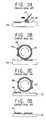
- FIG. 4is cross-sectional view of an exemplary printing device in accordance with the present invention.
- FIG. 5is a cross-sectional view of another exemplary printing device in accordance with the present invention.
- FIGS. 6A to 6 Earc cross-sectional views of an exemplary sequential printing process of a gravture offset method in accordance with the present invention.
- FIGS. 7A to 7 Eare cross-sectional views of an exemplary sequential printing process of a transfer offset method in accordance with the present invention.
- photoresist or ink materialsmay be used to during fabrication processes for forming a thin film transistor, a color filter, and a black matrix of a liquid crystal display device.
- the following processesmay be used to fabricate a thin film transistor, a color filter, and a black matrix of a liquid crystal display device.
- FIG. 4is cross-sectional view of an exemplary printing device in accordance with the present invention
- the printing devicemay include clean chamber 41 having a cliché and a UV light source system 42 disposed therein.
- the clean chamber 41may include an actuator 44 contacting a bottom portion of the cliché to affect a vertical movement of the cliché within the clean chamber 41 .
- the clichémay include a plurality of grooves 26 formed within an upper portion of the cliché. Although each of the plurality of grooves 26 are shown to have a rectangular geometry, other geometrical shapes such as triangular, semi-circular, and semi-elliptical geometrical shapes may be used.
- each the plurality of grooves 26may include any number of different combinations of geometrical shapes such as rectangular and semi-circular geometrical shapes, for example
- the UV light source system 42may function as a cleaning system for removing organic particles that may remain on the cliché after processing, thereby preventing an transfer of contamination.
- a gas inlet system 45may be provided to further clean the cliché of contaminates.
- the gas inlet system 45may supply a single gas or multiple gases 43 .
- the gas inlet system 45may supply ozone for cleaning of the cliché Accordingly, the cliché may remain within the clean chamber 41 to prevent contamination within the plurality of grooves 26 as well as on the uppermost surface of the cliché
- FIGS 6 A to 6 Eare cross-sectional views of an exemplary sequential printing process of a gravure offset method in accordance with the present invention.
- a clichémay he placed at a first position within an interior space of a clean chamber 41 , whereby contaminates, such as organic particles, may be removed from a plurality of grooves 26 of the cliché, as well as uppermost surfaces of the cliché using a UV lamp system 42 or a gas inlet system (not shown).
- a bottom portion of the clichémay be positioned upon the actuator 44 . Accordingly, the cliché 23 is cleaned within the interior of the clean chamber 41
- the clean chamber 41is shown to have a rectangular shape, ally geometrical shape may be used
- an opening 46is created at an uppermost portion of the clean chamber 41 .
- the opening 46may created by using any one of a slideable, hinged, or rotating door, for example.
- the clichémay be elevated via the actuator 44 to a position within the opening 46 .
- the uppermost surface of the clichémay be planar with an uppermost exterior surface of the clean chamber 41 .
- the uppermost surface of the clichémay extend slightly above, or be recessed slightly below the uppermost exterior surface of the clean chamber 41
- a photoresist or ink material 29may be filled into a plurality of grooves 26 formed in the uppermost surface or the cliché, wherein the plurality of grooves arc spaced apart to define a pattern.
- any excess photoresist material 29 that remains on the uppermost surface of the clichémay be removed by a doctor blade 27 . Accordingly, the photoresist material 29 may only remain in each of the plurality of grooves 26 Alternatively, as previously described, the uppermost surface of the cliché may be recessed below the uppermost exterior surface of the clean chamber 41 , wherein the photoresist material may exist within each of the plurality of grooves 26 and along the uppermost surface of the cliché.
- each of the plurality of grooves 26are shown to have a rectangular geometry, other geometrical shapes such as triangular, semi-circular, and semi-elliptical geometrical shapes may be used. Alternatively, each the plurality of grooves 26 may include any number of different combinations of geometrical shapes such as rectangular and semi-circular geometrical shapes, for example.
- a roller 25may be rolled across the uppermost surface of the cliché along a first direction so that individual photoresist material portions 24 of the photoresist material 29 (in FIG. 6C) that filled each of the plurality of grooves 26 (in FIG. 6C) are temporarily bonded onto a silicon blanket 28 of the roller 25 . Accordingly, the pattern of the photoresist-filled grooves 26 (in FIG. 6C) is transferred onto the silicon blanket 28 as the individual photoresist material portions 24
- the clichémay be returned to the interior of the clean chamber 41 by the actuator 44 , and the roller 25 with the individual photoresist material portions 24 may be relocated to another region for additional processing.
- the clean chamber 41may be scaled by closing the opening 46 (in FIG 6 B.) Accordingly, once the clean chamber 41 is sealed and the cliché returned to the first position, the cliché may be cleaned using one or both of the UV light source system 42 (in FIG. 6A) and the gas inlet system (not shown).
- the roller 25 having the individual photoresist material portions 24 attached to the silicon blanket 28may be positioned above an uppermost surface of a substrate 10
- the rollermay roll across the uppermost surface of the substrate 10 , thereby transferring the individual photoresist material portions 24 from the silicon blanket 28 onto the uppermost surface of the substrate 10 .
- the pattern of the photoresist-filled grooves 26(in FIG. 6C) is transferred onto the uppermost surface of the substrate 10 as the individual photoresist material portions 24 .
- the substrate 10 and the individual photoresist material portions 24may subsequently undergo additional processing.
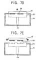
- FIGS 7 A to 7 Eare cross-sectional views of an exemplary sequential printing process of a transfer offset method in accordance with the present invention.
- a clichémay be placed at a first position with an interior space of a clean chamber 41 , whereby contaminates, such as organic particles, may be removed from a plurality of grooves 26 of the cliché, as well as uppermost surfaces of the cliché using or a gas inlet system 45 or a UV lamp system (not shown).
- a bottom portion of the clichémay be positioned upon the actuator 44 . Accordingly, the cliché is cleaned within the interior of the clean chamber 41
- the clean chamber 41is shown to have a rectangular shape, any geometrical shape may be used.
- an opening 46is created at an uppermost portion of the clean chamber 41 .
- the opening 46may created by using any one of a slidcable, hinged, or rotating door, for example.
- the clichémay be elevated via the actuator 44 to a position within the opening 46 Accordingly, the uppermost surface of the cliché may be planar with an uppermost exterior surface of the clean chamber 41 .
- the uppermost surface of the clichémay extend slightly above, or be recessed slightly below the uppermost exterior surface of the clean chamber 41 .
- a photoresist or ink material 29may be filled into a plurality of grooves 26 formed in the uppermost surface of the cliché, wherein the plurality of grooves arc spaced apart to define a pattern.
- any excess photoresist material 29 that remains on the uppermost surface of the clichémay be removed by a doctor blade 27 . Accordingly, the photoresist material 29 may only remain in each of the plurality of grooves 26 .
- the uppermost surface of the clichémay be recessed below the uppermost exterior surface of the clean chamber 41 , wherein the photoresist material may exist within each of the plurality of grooves 26 and along the uppermost surface of the cliché.
- each of the plurality of grooves 26are shown to have a rectangular geometry, other geometrical shapes such as triangular, semi-circular, and semi-elliptical geometrical shapes may be used Alternatively, each the plurality of grooves 26 may include any number of different combinations of geometrical shapes such as rectangular and semi-circular geometrical shapes, for example.
- a surface of a substrate 10which may be formed of a glass or plastic material, may be placed upon the surface of the cliché to contact uppermost surfaces of individual photoresist material portions 24 filled in each of plurality of grooves 26 (in FIG. 7C). Then, heat and/or pressure may be applied to the substrate 10 and cliché to bond each of the individual photoresist material portions 24 onto the surface of the substrate 10 . Accordingly, the pattern of the photoresist-filled rectangular grooves 26 (in FIG. 7C) may be transferred onto the surface of the substrate 10 blanket 28 as the individual photoresist material portions 24 .
- the substrate 10may be removed from the surface of the cliché along a vertical direction, and the individual photoresist material portions 24 may be transferred from the plurality of grooves 26 (in FIG. 7C) onto the surface of the substrate 10 , thereby completing the printing process for forming the pattern of the individual photoresist material portions 24 .
- the substrate 10may delivered to a position in which the individual photoresist material portions 24 are prepared for additional processing.
- the clichémay be returned to the interior of the clean chamber 41 by the actuator 44 .
- the clean chamber 41may be sealed by closing the opening 46 (in FIG. 7B). Accordingly, once the clean chamber 41 is sealed and the cliché returned to the first position, the cliché may be cleaned using one or both of the gas inlet system 48 (in FIG. 7A) of the UV light source system (not shown)
- the cliché 23may be kept within the interior of the clean chamber 41 once transfer of the individual photoresist material portions 24 is completed, whereby contaminates are prevented from being introduced onto surfaces of the cliché
- the clichémay undergo cleaning after each printing process is completed.
Landscapes
- Physics & Mathematics (AREA)
- General Physics & Mathematics (AREA)
- Optics & Photonics (AREA)
- Nonlinear Science (AREA)
- Chemical & Material Sciences (AREA)
- Crystallography & Structural Chemistry (AREA)
- Optical Filters (AREA)
- Printing Methods (AREA)
- Exposure And Positioning Against Photoresist Photosensitive Materials (AREA)
- Liquid Crystal (AREA)
Abstract
Description
- The present invention claims the benefit of Korean Patent Application No 67236/2001 filled in Korea on Oct. 30, 2001, which is hereby incorporated by reference.[0001]
- 1. Field of the Invention[0002]
- The present invention relates to a printing system and method used for fabricating a liquid crystal display device, and more particularly, to a printing system and printing method for fabricating a thin film transistor, a color filter, and a black matrix of a liquid crystal display device[0003]
- 2. Description of the Related Art[0004]
- In general, cathode ray tube (CRT) monitors are commonly used to display information on a computer displays and televisions because of the CRT monitor's superior picture quality and image brightness. However, as demand for larger displays increases, the size of the CRT monitors also increases. Accordingly, the overall size of the CRT monitor eventually increases to a point where it's size is too large to efficiently display image data. In addition, mobility of the CRT monitor decreases as overall weight of the CRT monitor increases.[0005]
- Presently, flat type display devices, such as liquid crystal displays (LCD's), plasma display panel (PDP) displays, organic electro luminescence (EL) displays, light emitting diodes (LEDs), and field emission displays have gained in popularity. Among the different flat panel display devices, liquid crystal display (LCD) devices have been developed as monitors for laptop and desktop computers because of their low power consumption[0006]
- FIG. 1 is a cross-sectional view of an LCD device panel according to the conventional art. In FIG. 1, the LCD device panel is formed of a lower substrate and an upper substrate. The upper substrate includes a[0007]
glass substrate 10 having acolor filter layer 11, ablack matrix 12, anorientation layer 14, and acommon electrode 13. Both theblack matrix 12 and thecolor filter layer 11 are formed on theglass substrate 10, wherein theblack matrix 12 is disposed between adjacentcolor filter layers 11. Thecolor filter layer 11 includes a resin film containing dye or three basic colors of red, green, and blue or a pigment thereof. An overcoat film (not shown) is provided for smoothing thecolor filter layer 11 and improving an adhesive force with thecommon electrode 13, which is commonly formed of a transparent conductive material, such as indium tin oxide (ITO). Theorientation layer 14 aligns a liquid crystal material formed between the upper and lower substrates. - In FIG. 1, the lower substrate includes a[0008]
glass substrate 10 having a thin film transistor (TFT) formed thereon, aprotection film 20, apixel electrode 21, and anorientation layer 14 The TFT includes agate electrode 15, anactive layer 16, asource electrode 18, and adrain electrode 19. Thegate electrode 15 is formed on theglass substrate 10 with agate insulating layer 17 formed on thegate electrode 15 and theglass substrate 10. Theactive layer 16 includes asemiconductor layer 16aformed by depositing an amorphous silicon (a-Si) and a n+dopedohmic contact layer 16bat opposing upper portions of thesemiconductor layer 16a. Theprotection film 20 is formed to cover the TFT and thegate insulating film 17. Thepixel electrode 21 is formed on theprotection film 20 and is formed of a transparent conductive material, such ITO Theorientation layer 14 is formed on thepixel electrode 21 and theprotection film 20. Polarizingfilms 22 are disposed on the outside surfaces of the upper and lower substrate respectively - In FIG. 1, light transmittance through the liquid crystal layer formed between the upper and lower substrates is controlled by application of an electric potential on the[0009]
common electrode 13 and thepixel electrode 21. Thecommon electrode 13 commonly receives a constant potential, whereas thepixel electrode 21 receives a data signal to generate the electric field. Thepixel electrode 21 receives the data signal when the TFT is turned on. Specifically, a data signal is supplied to thesource electrode 18 of the TFT and is transmitted via theactive layer 16athrough theohmic contact layer 16bwhen thegate electrode 15 is enabled by receiving a scan signal. Accordingly, the data signal is transmitted to thedrain electrode 19 and applied to thepixel electrode 21, thereby generating the electric field in combination with thecommon electrode 13 and controlling the light transmitted through the liquid crystal layer. - Fabrication of the LCD device commonly includes a thin film deposition process, a photolithographic process, and an etching process that are repeatedly performed. Moreover, fabrication of the TFT, the[0010]
color filter layer 11, and theblack matrix 12 includes sequential printing processes of ink or photoresist materials. The printing processes include a gravure offset method and a transfer method depending upon how the photoresist material is applied to the upper mid lower substrates. The gravure offset method includes steps of filling the photoresist material into a groove of a cliché, transferring the photoresist material filled in the groove onto a roller; and applying the transferred photoresist material onto the upper or lower substrate. - FIGS. 2A to[0011]2D are cross-sectional views of a sequential printing process according to a gravure offset printing method according to the conventional art. In FIG. 2A, a photoresist or
ink material 29 is filled into a plurality ofrectangular grooves 26 formed in a surface of a cliché, wherein the plurality of rectangular grooves are spaced apart to define a pattern Next, any excessphotoresist material 29 that remains on the surface of the cliché is removed by adoctor blade 27. Accordingly, thephotoresist material 29 only remains in each of the plurality ofrectangular grooves 26 - In FIG. 2B, a[0012]
roller 25 is rolled across the surface of the cliché along a first direction so that individual photoresistmaterial portions 24 of the photoresist material29 (in FIG. 2A) that filled each of the plurality of rectangular grooves26 (in FIG. 2A) are temporarily bonded onto ablanket 28 or theroller 25 Accordingly, the pattern of the photoresist-filled rectangular grooves26 (in FIG. 2A) is transferred onto theblanket 28 as the individual photoresistmaterial portions 24. - In FIG. 2C, the[0013]
roller 25 is placed above asubstrate 10 and the individualphotoresist material portions 24 are transferred onto a surface of thesubstrate 10 corresponding to the pattern of the photoresist-filled rectangular grooves26 (in FIG. 2A). Thesubstrate 10 may be formed of a glass or plastic substrate material. - In FIG,[0014]2D, the individual photoresist
material portions 24 are completely transferred to the surface of thesubstrate 10, and the printing process is completed Thus, the pattern of the grooves26 (in FIG. 2A) is replicated onto the surface of thesubstrate 10. - FIGS. 3A to[0015]3D are cross-sectional views of a sequential printing process according to a transfer method according to the conventional art. In FIG. 3A, a photoresist or
ink material 29 is filled into a plurality ofrectangular grooves 26 formed in a surface of a cliché, wherein the plurality of rectangular grooves are spaced apart to define a pattern. Next, any excessphotoresist material 29 that remains on the surface of the cliché is removed by adoctor blade 27. Accordingly, thephotoresist material 29 only remains in each of the plurality ofrectangular grooves 26 - In FIG. 3B, a surface of a[0016]
substrate 10, which may be formed of a glass or plastic material, is placed upon the surface of the cliché to contact uppermost surfaces of individual photoresistmaterial portions 24 filled in each of plurality of rectangular grooves26 (in FIG. 3A). Then, heat and/or pressure is applied to thesubstrate 10 and cliché to bond each of the individual photoresistmaterial portions 24 onto the surface of thesubstrate 10 Accordingly, the pattern of the photoresist-filled rectanglar grooves26 (in FIG. 3A) is transferred onto the surface of thesubstrate 10blanket 28 as the individual photoresistmaterial portions 24. - In FIG. 3C, the[0017]
substrate 10 is removed from the surface of the cliché, and the individual photoresistmaterial portions 24 are transferred from the plurality of rectangular grooves26 (in FIG. 3A) onto the surface of thesubstrate 10, thereby completing the printing process for forming the pattern. - In FIG. 3D, the[0018]
substrate 10 is delivered to a position in which the individualphotoresist material portions 24 are prepared for additional processing. - However, both the gravue and transfer printing methods according to the conventional art are problematic. Since the cliché is exposed to an ambient atmosphere in the gravue and transfer printing methods according to the conventional art, the cliché may become contaminated, thus causing contamination of the[0019]
substrate 10 and possibly disrupting transfer of the photoresist pattern onto thesubstrate 10. - Accordingly, the present invention is directed to a printing system and method for fabricating a liquid crystal display device that substantially obviates one or more of the problems due to limitations and disadvantages of the related art[0020]
- An object of the present invention is to provide a printing system and method for fabricating a liquid crystal display device that reduces contamination of a photoresist pattern.[0021]
- Additional features and advantages of the invention will be set forth in the description which follows, and in part will be apparent from the description, or may be learned by practice of the invention. The objectives and other advantages of the invention will be realized and attained by the structure particularly pointed out in the written description and claims hereof as well as the appended drawings.[0022]
- To achieve these and other advantages and in accordance with the purpose of the present invention, as embodied and broadly described, a printing system for printing a pattern onto a liquid crystal display device includes a cliché having a plurality of grooves defining a pattern, a blade for filling a material into each of the plurality of grooves of the cliché, a clean chamber for cleaning the cliché, and an actuator disposed within an interior of the clean chamber upon which the cliché is placed.[0023]
- In another aspect, a printing method of forming a printing pattern of a liquid crystal display device includes ascending a cliché from a first position within an interior of a clean chamber, introducing a material into a plurality of grooves of the cliché, removing the material from a surface of the cliché using a blade, transferring the material from the plurality of grooves onto a roller, and applying the transferred material onto a substrate.[0024]
- In another aspect, a printing method of forming a printing pattern of a liquid crystal display device includes ascending a cliché from a first position within an interior of a clean chamber, introducing a material into a plurality of grooves of the cliché removing the material from a surface of the cliché using a blade, attaching a first surface of a substrate onto an uppermost surface of the cliché for transferring the material from the plurality of grooves onto the first surface of the substrate, and removing the substrate from the uppermost surface of the cliché.[0025]
- It is to be understood that both the foregoing general description and the following detailed description are exemplary and explanatory and are intended to provide further explanation of the invention as claimed.[0026]
- The accompanying drawings, which are included to provide a further understanding of the invention and are incorporated in and constitute a part of this specification, illustrate embodiments of the invention and together with the description serve to explain the principles of the invention. In the drawings:[0027]
- FIG. 1 is a cross-sectional view of a liquid crystal display device panel according to the conventional art;[0028]
- FIGS. 2A to[0029]2D are cross-sectional views of a sequential printing process according to a gravure offset method according to the conventional art;
- FIGS[0030]3A to3D are cross-sectional views of a sequential printing process according to a transfer method according to the conventional art;
- FIG. 4 is cross-sectional view of an exemplary printing device in accordance with the present invention;[0031]
- FIG. 5 is a cross-sectional view of another exemplary printing device in accordance with the present invention;[0032]
- FIGS. 6A to[0033]6E arc cross-sectional views of an exemplary sequential printing process of a gravture offset method in accordance with the present invention; and
- FIGS. 7A to[0034]7E are cross-sectional views of an exemplary sequential printing process of a transfer offset method in accordance with the present invention.
- Reference will now be made in detail to the preferred embodiments of the present invention, examples of which are illustrated in the accompanying drawings.[0035]
- Although the following description refers to a photoresist or ink materials in general, it is to be understood that the photoresist or ink materials may be used to during fabrication processes for forming a thin film transistor, a color filter, and a black matrix of a liquid crystal display device. Likewise, it is to be understood that the following processes may used to fabricate a thin film transistor, a color filter, and a black matrix of a liquid crystal display device.[0036]
- FIG. 4 is cross-sectional view of an exemplary printing device in accordance with the present invention In FIG. 4, the printing device may include[0037]
clean chamber 41 having a cliché and a UVlight source system 42 disposed therein. Theclean chamber 41 may include anactuator 44 contacting a bottom portion of the cliché to affect a vertical movement of the cliché within theclean chamber 41. The cliché may include a plurality ofgrooves 26 formed within an upper portion of the cliché. Although each of the plurality ofgrooves 26 are shown to have a rectangular geometry, other geometrical shapes such as triangular, semi-circular, and semi-elliptical geometrical shapes may be used. Alternatively, each the plurality ofgrooves 26 may include any number of different combinations of geometrical shapes such as rectangular and semi-circular geometrical shapes, for example The UVlight source system 42 may function as a cleaning system for removing organic particles that may remain on the cliché after processing, thereby preventing an transfer of contamination. - In FIG. 5, in addition to, or instead of the UV light source system[0038]42 (in FIG. 4), a
gas inlet system 45 may be provided to further clean the cliché of contaminates. Thegas inlet system 45 may supply a single gas ormultiple gases 43. For example, thegas inlet system 45 may supply ozone for cleaning of the cliché Accordingly, the cliché may remain within theclean chamber 41 to prevent contamination within the plurality ofgrooves 26 as well as on the uppermost surface of the cliché - FIGS[0039]6A to6E are cross-sectional views of an exemplary sequential printing process of a gravure offset method in accordance with the present invention. In FIG. 6A, a cliché may he placed at a first position within an interior space of a
clean chamber 41, whereby contaminates, such as organic particles, may be removed from a plurality ofgrooves 26 of the cliché, as well as uppermost surfaces of the cliché using aUV lamp system 42 or a gas inlet system (not shown). A bottom portion of the cliché may be positioned upon theactuator 44. Accordingly, thecliché 23 is cleaned within the interior of theclean chamber 41 Although theclean chamber 41 is shown to have a rectangular shape, ally geometrical shape may be used - In FIG. 6B, an[0040]
opening 46 is created at an uppermost portion of theclean chamber 41. Theopening 46 may created by using any one of a slideable, hinged, or rotating door, for example. Once theopening 46 has been created, the cliché may be elevated via theactuator 44 to a position within theopening 46. Accordingly, the uppermost surface of the cliché may be planar with an uppermost exterior surface of theclean chamber 41. Alternatively, the uppermost surface of the cliché may extend slightly above, or be recessed slightly below the uppermost exterior surface of theclean chamber 41 - In FIG. 6C, a photoresist or[0041]
ink material 29 may be filled into a plurality ofgrooves 26 formed in the uppermost surface or the cliché, wherein the plurality of grooves arc spaced apart to define a pattern. Next, anyexcess photoresist material 29 that remains on the uppermost surface of the cliché may be removed by adoctor blade 27. Accordingly, thephotoresist material 29 may only remain in each of the plurality ofgrooves 26 Alternatively, as previously described, the uppermost surface of the cliché may be recessed below the uppermost exterior surface of theclean chamber 41, wherein the photoresist material may exist within each of the plurality ofgrooves 26 and along the uppermost surface of the cliché. - Although each of the plurality of[0042]
grooves 26 are shown to have a rectangular geometry, other geometrical shapes such as triangular, semi-circular, and semi-elliptical geometrical shapes may be used. Alternatively, each the plurality ofgrooves 26 may include any number of different combinations of geometrical shapes such as rectangular and semi-circular geometrical shapes, for example. - In FIG. 6D, a[0043]
roller 25 may be rolled across the uppermost surface of the cliché along a first direction so that individualphotoresist material portions 24 of the photoresist material29 (in FIG. 6C) that filled each of the plurality of grooves26 (in FIG. 6C) are temporarily bonded onto asilicon blanket 28 of theroller 25. Accordingly, the pattern of the photoresist-filled grooves26 (in FIG. 6C) is transferred onto thesilicon blanket 28 as the individualphotoresist material portions 24 - When transfer of the individual[0044]
photoresist pattern portions 24 onto thesilicon blanket 28 of theroller 24 is complete, the cliché may be returned to the interior of theclean chamber 41 by theactuator 44, and theroller 25 with the individualphotoresist material portions 24 may be relocated to another region for additional processing. Once the cliché has been returned to the interior of theclean chamber 41, theclean chamber 41 may be scaled by closing the opening46 (in FIG6B.) Accordingly, once theclean chamber 41 is sealed and the cliché returned to the first position, the cliché may be cleaned using one or both of the UV light source system42 (in FIG. 6A) and the gas inlet system (not shown). - In FIG. 6E, the[0045]
roller 25 having the individualphotoresist material portions 24 attached to thesilicon blanket 28 may be positioned above an uppermost surface of asubstrate 10 The roller may roll across the uppermost surface of thesubstrate 10, thereby transferring the individualphotoresist material portions 24 from thesilicon blanket 28 onto the uppermost surface of thesubstrate 10. Accordingly, the pattern of the photoresist-filled grooves26 (in FIG. 6C) is transferred onto the uppermost surface of thesubstrate 10 as the individualphotoresist material portions 24. Thesubstrate 10 and the individualphotoresist material portions 24 may subsequently undergo additional processing. - FIGS[0046]7A to7E are cross-sectional views of an exemplary sequential printing process of a transfer offset method in accordance with the present invention. In FIG. 7A, a cliché may be placed at a first position with an interior space of a
clean chamber 41, whereby contaminates, such as organic particles, may be removed from a plurality ofgrooves 26 of the cliché, as well as uppermost surfaces of the cliché using or agas inlet system 45 or a UV lamp system (not shown). A bottom portion of the cliché may be positioned upon theactuator 44. Accordingly, the cliché is cleaned within the interior of theclean chamber 41 Although theclean chamber 41 is shown to have a rectangular shape, any geometrical shape may be used. - In FIG[0047]7B, an
opening 46 is created at an uppermost portion of theclean chamber 41. Theopening 46 may created by using any one of a slidcable, hinged, or rotating door, for example. Once theopening 46 has been created, the cliché may be elevated via theactuator 44 to a position within theopening 46 Accordingly, the uppermost surface of the cliché may be planar with an uppermost exterior surface of theclean chamber 41. Alternatively, the uppermost surface of the cliché may extend slightly above, or be recessed slightly below the uppermost exterior surface of theclean chamber 41. - In FIG. 7C, a photoresist or[0048]
ink material 29 may be filled into a plurality ofgrooves 26 formed in the uppermost surface of the cliché, wherein the plurality of grooves arc spaced apart to define a pattern. Next, anyexcess photoresist material 29 that remains on the uppermost surface of the cliché may be removed by adoctor blade 27. Accordingly, thephotoresist material 29 may only remain in each of the plurality ofgrooves 26. Alternatively, as previously described, the uppermost surface of the cliché may be recessed below the uppermost exterior surface of theclean chamber 41, wherein the photoresist material may exist within each of the plurality ofgrooves 26 and along the uppermost surface of the cliché. - Although each of the plurality of[0049]
grooves 26 are shown to have a rectangular geometry, other geometrical shapes such as triangular, semi-circular, and semi-elliptical geometrical shapes may be used Alternatively, each the plurality ofgrooves 26 may include any number of different combinations of geometrical shapes such as rectangular and semi-circular geometrical shapes, for example. - In FIG. 7D, a surface of a[0050]
substrate 10, which may be formed of a glass or plastic material, may be placed upon the surface of the cliché to contact uppermost surfaces of individualphotoresist material portions 24 filled in each of plurality of grooves26 (in FIG. 7C). Then, heat and/or pressure may be applied to thesubstrate 10 and cliché to bond each of the individualphotoresist material portions 24 onto the surface of thesubstrate 10. Accordingly, the pattern of the photoresist-filled rectangular grooves26 (in FIG. 7C) may be transferred onto the surface of thesubstrate 10blanket 28 as the individualphotoresist material portions 24. - In FIG. 7E, the[0051]
substrate 10 may be removed from the surface of the cliché along a vertical direction, and the individualphotoresist material portions 24 may be transferred from the plurality of grooves26 (in FIG. 7C) onto the surface of thesubstrate 10, thereby completing the printing process for forming the pattern of the individualphotoresist material portions 24. Next, thesubstrate 10 may delivered to a position in which the individualphotoresist material portions 24 are prepared for additional processing. - When transfer of the individual[0052]
photoresist pattern portions 24 onto the surface of thesubstrate 10 is complete, the cliché may be returned to the interior of theclean chamber 41 by theactuator 44. Once the cliché has been returned to the interior of theclean chamber 41, theclean chamber 41 may be sealed by closing the opening46 (in FIG. 7B). Accordingly, once theclean chamber 41 is sealed and the cliché returned to the first position, the cliché may be cleaned using one or both of the gas inlet system48 (in FIG. 7A) of the UV light source system (not shown) - Accordingly, the[0053]
cliché 23 may be kept within the interior of theclean chamber 41 once transfer of the individualphotoresist material portions 24 is completed, whereby contaminates are prevented from being introduced onto surfaces of the cliché In addition, the cliché may undergo cleaning after each printing process is completed. - It will be apparent to those skilled in the art that various modifications and variations can be made in the printing device and method for fabricating a liquid crystal display device of the present invention without departing from the spirit or scope of the invention Thus, it is intended that the present invention cover the modifications and variations of this invention provided they come within the scope of the appended claims and their equivalents.[0054]
Claims (30)
Priority Applications (1)
| Application Number | Priority Date | Filing Date | Title |
|---|---|---|---|
| US11/004,833US7312094B2 (en) | 2001-10-30 | 2004-12-07 | Printing system and method for fabricating a liquid crystal display device |
Applications Claiming Priority (3)
| Application Number | Priority Date | Filing Date | Title |
|---|---|---|---|
| KR1020010067236AKR100675624B1 (en) | 2001-10-30 | 2001-10-30 | Pattern Forming Device of Liquid Crystal Display Device by Printing Method and Pattern Forming Method of Liquid Crystal Display Device Using the Same |
| KR67236/2001 | 2001-10-30 | ||
| KR2001-67236 | 2001-10-30 |
Related Child Applications (1)
| Application Number | Title | Priority Date | Filing Date |
|---|---|---|---|
| US11/004,833DivisionUS7312094B2 (en) | 2001-10-30 | 2004-12-07 | Printing system and method for fabricating a liquid crystal display device |
Publications (2)
| Publication Number | Publication Date |
|---|---|
| US20030081095A1true US20030081095A1 (en) | 2003-05-01 |
| US6835583B2 US6835583B2 (en) | 2004-12-28 |
Family
ID=19715534
Family Applications (2)
| Application Number | Title | Priority Date | Filing Date |
|---|---|---|---|
| US10/183,480Expired - LifetimeUS6835583B2 (en) | 2001-10-30 | 2002-06-28 | Printing system and method for fabricating a liquid crystal display device |
| US11/004,833Expired - LifetimeUS7312094B2 (en) | 2001-10-30 | 2004-12-07 | Printing system and method for fabricating a liquid crystal display device |
Family Applications After (1)
| Application Number | Title | Priority Date | Filing Date |
|---|---|---|---|
| US11/004,833Expired - LifetimeUS7312094B2 (en) | 2001-10-30 | 2004-12-07 | Printing system and method for fabricating a liquid crystal display device |
Country Status (2)
| Country | Link |
|---|---|
| US (2) | US6835583B2 (en) |
| KR (1) | KR100675624B1 (en) |
Cited By (11)
| Publication number | Priority date | Publication date | Assignee | Title |
|---|---|---|---|---|
| US20030124866A1 (en)* | 2001-12-31 | 2003-07-03 | Lg.Philips Lcd Co., Ltd. | Method and apparatus for forming pattern using printing method |
| US20040125330A1 (en)* | 2002-12-27 | 2004-07-01 | Lg.Philips Lcd Co., Ltd. | Method for forming pattern of liquid crystal display device |
| WO2005039885A1 (en) | 2003-10-22 | 2005-05-06 | Koninklijke Philips Electronics N.V. | A device and method for printing features onto a substrate |
| WO2005075214A1 (en) | 2004-02-06 | 2005-08-18 | Koninklijke Philips Electronics N.V. | Printing |
| US20070048448A1 (en)* | 2005-08-17 | 2007-03-01 | Kim Dae H | Patterning method using coatings containing ionic components |
| EP1791018A1 (en)* | 2005-11-28 | 2007-05-30 | LG. Philips LCD Co. Ltd. | Printing system and method for manufacturing a liquid crystal display device using the same |
| JP2007144983A (en)* | 2005-11-28 | 2007-06-14 | Lg Philips Lcd Co Ltd | Printing apparatus system and pattern forming method using the same |
| JP2007182052A (en)* | 2005-12-29 | 2007-07-19 | Lg Philips Lcd Co Ltd | Printing apparatus and printing method |
| US20080000374A1 (en)* | 2006-06-21 | 2008-01-03 | L.G.Philips Lcd Co., Ltd. | Printing apparatus, patterning method, and method of fabricating liquid crystal display device using the same |
| US20090208661A1 (en)* | 2005-12-29 | 2009-08-20 | Chul Ho Kim | Printing apparatus for liquid crystal display device and pattern forming method using the same |
| US20100159788A1 (en)* | 2006-06-30 | 2010-06-24 | Chul Ho Kim | Printing device, patterning method using the same, and method of fabricating a liquid crystal display device using the same |
Families Citing this family (11)
| Publication number | Priority date | Publication date | Assignee | Title |
|---|---|---|---|---|
| JP3698749B2 (en)* | 1995-01-11 | 2005-09-21 | 株式会社半導体エネルギー研究所 | Liquid crystal cell manufacturing method and apparatus, and liquid crystal cell production system |
| KR20030057067A (en)* | 2001-12-28 | 2003-07-04 | 엘지.필립스 엘시디 주식회사 | A method of forming pattern using printing process |
| US6956308B2 (en)* | 2003-07-15 | 2005-10-18 | Nikon Corporation | Dual flow circulation system for a mover |
| US7582331B2 (en)* | 2005-06-30 | 2009-09-01 | Lg. Display Co., Ltd. | Printing apparatus and fabricating method thereof |
| KR101138428B1 (en)* | 2005-09-06 | 2012-04-26 | 삼성전자주식회사 | Printing apparatus of ink pattern, method for fabricating ink pattern and liquid crystal display using the same |
| KR100922797B1 (en)* | 2005-12-29 | 2009-10-21 | 엘지디스플레이 주식회사 | Pattern Forming Device and Forming Method |
| KR101192748B1 (en)* | 2005-12-30 | 2012-10-18 | 엘지디스플레이 주식회사 | Printing Apparatus and Method of manufacturing Liquid Crystal Display Device using the same |
| WO2007117698A2 (en) | 2006-04-07 | 2007-10-18 | Qd Vision, Inc. | Composition including material, methods of depositing material, articles including same and systems for depositing material |
| WO2008111947A1 (en) | 2006-06-24 | 2008-09-18 | Qd Vision, Inc. | Methods and articles including nanomaterial |
| KR101308458B1 (en)* | 2007-03-30 | 2013-09-16 | 엘지디스플레이 주식회사 | Printing device and method for forming pattern using the same |
| KR20120014500A (en)* | 2010-08-09 | 2012-02-17 | 삼성전자주식회사 | Desorption plate, manufacturing method of the desorption plate, and patterns formed by the roll printing method |
Citations (5)
| Publication number | Priority date | Publication date | Assignee | Title |
|---|---|---|---|---|
| US5678483A (en)* | 1994-02-16 | 1997-10-21 | Corning Incorporated | Method for printing a black border for a color filter |
| US6001515A (en)* | 1993-11-03 | 1999-12-14 | Corning Incorporated | Method for printing a color filter |
| US6730356B2 (en)* | 2001-12-31 | 2004-05-04 | Lg.Philips Lcd Co., Ltd. | Method and apparatus for forming pattern using printing method |
| US6732643B2 (en)* | 2001-11-07 | 2004-05-11 | Lg. Philips Lcd Co., Ltd. | Method for forming pattern using printing process |
| US6759348B1 (en)* | 2002-12-31 | 2004-07-06 | Lg.Philips Lcd Co., Ltd. | Pattern and its forming method of liquid crystal display device |
Family Cites Families (4)
| Publication number | Priority date | Publication date | Assignee | Title |
|---|---|---|---|---|
| JPH0580530A (en)* | 1991-09-24 | 1993-04-02 | Hitachi Ltd | Production of thin film pattern |
| JP2955990B2 (en)* | 1996-06-28 | 1999-10-04 | 株式会社沖電気コミュニケーションシステムズ | Screen plate cleaning device |
| US6132523A (en)* | 1997-09-19 | 2000-10-17 | Sharp Kabushiki Kaisha | Method of cleaning a substrate in a cleaning tank using plural fluid flows |
| JP2000117954A (en)* | 1998-10-16 | 2000-04-25 | Tani Denki Kogyo Kk | Method and apparatus for cleaning screen printing plate, and the screen printing plate |
- 2001
- 2001-10-30KRKR1020010067236Apatent/KR100675624B1/ennot_activeExpired - Fee Related
- 2002
- 2002-06-28USUS10/183,480patent/US6835583B2/ennot_activeExpired - Lifetime
- 2004
- 2004-12-07USUS11/004,833patent/US7312094B2/ennot_activeExpired - Lifetime
Patent Citations (5)
| Publication number | Priority date | Publication date | Assignee | Title |
|---|---|---|---|---|
| US6001515A (en)* | 1993-11-03 | 1999-12-14 | Corning Incorporated | Method for printing a color filter |
| US5678483A (en)* | 1994-02-16 | 1997-10-21 | Corning Incorporated | Method for printing a black border for a color filter |
| US6732643B2 (en)* | 2001-11-07 | 2004-05-11 | Lg. Philips Lcd Co., Ltd. | Method for forming pattern using printing process |
| US6730356B2 (en)* | 2001-12-31 | 2004-05-04 | Lg.Philips Lcd Co., Ltd. | Method and apparatus for forming pattern using printing method |
| US6759348B1 (en)* | 2002-12-31 | 2004-07-06 | Lg.Philips Lcd Co., Ltd. | Pattern and its forming method of liquid crystal display device |
Cited By (24)
| Publication number | Priority date | Publication date | Assignee | Title |
|---|---|---|---|---|
| US6730356B2 (en)* | 2001-12-31 | 2004-05-04 | Lg.Philips Lcd Co., Ltd. | Method and apparatus for forming pattern using printing method |
| US20030124866A1 (en)* | 2001-12-31 | 2003-07-03 | Lg.Philips Lcd Co., Ltd. | Method and apparatus for forming pattern using printing method |
| US20040125330A1 (en)* | 2002-12-27 | 2004-07-01 | Lg.Philips Lcd Co., Ltd. | Method for forming pattern of liquid crystal display device |
| US7140296B2 (en)* | 2002-12-27 | 2006-11-28 | Lg.Philips Lcd Co., Ltd. | Method for forming pattern of liquid crystal display device |
| US20070125252A1 (en)* | 2003-10-22 | 2007-06-07 | Koninklijke Philips Electronics N.V. | Device and method for printing features onto a substrate |
| WO2005039885A1 (en) | 2003-10-22 | 2005-05-06 | Koninklijke Philips Electronics N.V. | A device and method for printing features onto a substrate |
| WO2005075214A1 (en) | 2004-02-06 | 2005-08-18 | Koninklijke Philips Electronics N.V. | Printing |
| US20070048448A1 (en)* | 2005-08-17 | 2007-03-01 | Kim Dae H | Patterning method using coatings containing ionic components |
| EP1791018A1 (en)* | 2005-11-28 | 2007-05-30 | LG. Philips LCD Co. Ltd. | Printing system and method for manufacturing a liquid crystal display device using the same |
| US20070119322A1 (en)* | 2005-11-28 | 2007-05-31 | Chung In J | Printing system and method for manufacturing liquid crystal display device using the same |
| JP2007144984A (en)* | 2005-11-28 | 2007-06-14 | Lg Phillips Lcd Co Ltd | Printing system and liquid crystal display device manufacturing method using the same |
| JP2007144983A (en)* | 2005-11-28 | 2007-06-14 | Lg Philips Lcd Co Ltd | Printing apparatus system and pattern forming method using the same |
| US7658147B2 (en) | 2005-11-28 | 2010-02-09 | Lg. Display Co., Ltd. | Printing system and method for manufacturing liquid crystal display device using the same |
| US8720337B2 (en)* | 2005-11-28 | 2014-05-13 | Lg Display Co., Ltd. | Printing device system and patterning method using the same |
| US20100095860A1 (en)* | 2005-11-28 | 2010-04-22 | Lg Display Co., Ltd. | Printing system and method for manufacturing liquid crystal display device using the same |
| US20090223396A1 (en)* | 2005-11-28 | 2009-09-10 | Lg Display Co., Ltd. | Printing device system and patterning method using the same |
| JP2007182052A (en)* | 2005-12-29 | 2007-07-19 | Lg Philips Lcd Co Ltd | Printing apparatus and printing method |
| US20090208661A1 (en)* | 2005-12-29 | 2009-08-20 | Chul Ho Kim | Printing apparatus for liquid crystal display device and pattern forming method using the same |
| US7987782B2 (en)* | 2005-12-29 | 2011-08-02 | Lg Display Co., Ltd. | Printing apparatus for liquid crystal display device and pattern forming method using the same |
| KR101255294B1 (en)* | 2005-12-29 | 2013-04-23 | 엘지디스플레이 주식회사 | Printing Apparatus and Method of manufacturing Liquid Crystal Display Device using the same |
| CN101093353B (en)* | 2006-06-21 | 2012-07-18 | 乐金显示有限公司 | Printing apparatus, patterning method, and method of fabricating liquid crystal display device using the same |
| US20080000374A1 (en)* | 2006-06-21 | 2008-01-03 | L.G.Philips Lcd Co., Ltd. | Printing apparatus, patterning method, and method of fabricating liquid crystal display device using the same |
| US20100159788A1 (en)* | 2006-06-30 | 2010-06-24 | Chul Ho Kim | Printing device, patterning method using the same, and method of fabricating a liquid crystal display device using the same |
| US8601945B2 (en)* | 2006-06-30 | 2013-12-10 | Lg Display Co., Ltd. | Printing device, patterning method using the same, and method of fabricating a liquid crystal display device using the same |
Also Published As
| Publication number | Publication date |
|---|---|
| KR100675624B1 (en) | 2007-02-01 |
| KR20030035253A (en) | 2003-05-09 |
| US20050092712A1 (en) | 2005-05-05 |
| US7312094B2 (en) | 2007-12-25 |
| US6835583B2 (en) | 2004-12-28 |
Similar Documents
| Publication | Publication Date | Title |
|---|---|---|
| US6835583B2 (en) | Printing system and method for fabricating a liquid crystal display device | |
| US8210890B2 (en) | Method of fabricating organic electroluminescence display device comprising an elastic contact electrode | |
| US8147902B2 (en) | Electro luminescence display device and fabricating method and apparatus thereof | |
| US7452567B2 (en) | Method for fabricating color filter of liquid crystal display device | |
| US6940578B2 (en) | Method for fabricating liquid crystal display device | |
| US7243599B2 (en) | Method of fabricating color filter in display device | |
| KR101339170B1 (en) | Liquid crystal display panel and manufacturing method thereof | |
| KR100825316B1 (en) | Printing equipment and method for manufacturing liquid crystal display device | |
| US7331286B2 (en) | Method for fabricating color filter of liquid crystal display device | |
| US7140296B2 (en) | Method for forming pattern of liquid crystal display device | |
| US7520220B2 (en) | Cliché unit, printing apparatus, and printing method using the same | |
| US6999148B2 (en) | Apparatus, mask, and method for printing alignment layer | |
| US7745075B2 (en) | Method for fabricating color filter substrates | |
| US20040131861A1 (en) | Device and method for forming alignment layer of liquid crystal display device | |
| JP4041122B2 (en) | Liquid crystal display device and manufacturing method thereof | |
| US7316873B2 (en) | Method of manufacturing color filter substrate of liquid crystal display device | |
| KR100807584B1 (en) | Printing equipment and printing method for liquid crystal display | |
| CN100368907C (en) | Display device and manufacturing method thereof | |
| KR960014295B1 (en) | Manufacturing method of color filter for liquid crystal display device | |
| JPH07325308A (en) | Liquid crystal display device and manufacturing method thereof |
Legal Events
| Date | Code | Title | Description |
|---|---|---|---|
| AS | Assignment | Owner name:LG. PHILIPS LCD CO., LTD., KOREA, REPUBLIC OF Free format text:ASSIGNMENT OF ASSIGNORS INTEREST;ASSIGNORS:YI, JONG-HOON;LEE, DONG-HOON;REEL/FRAME:013063/0445 Effective date:20020628 | |
| FEPP | Fee payment procedure | Free format text:PAYER NUMBER DE-ASSIGNED (ORIGINAL EVENT CODE: RMPN); ENTITY STATUS OF PATENT OWNER: LARGE ENTITY Free format text:PAYOR NUMBER ASSIGNED (ORIGINAL EVENT CODE: ASPN); ENTITY STATUS OF PATENT OWNER: LARGE ENTITY | |
| STCF | Information on status: patent grant | Free format text:PATENTED CASE | |
| FPAY | Fee payment | Year of fee payment:4 | |
| AS | Assignment | Owner name:LG DISPLAY CO., LTD., KOREA, REPUBLIC OF Free format text:CHANGE OF NAME;ASSIGNOR:LG.PHILIPS LCD CO., LTD.;REEL/FRAME:021147/0009 Effective date:20080319 Owner name:LG DISPLAY CO., LTD.,KOREA, REPUBLIC OF Free format text:CHANGE OF NAME;ASSIGNOR:LG.PHILIPS LCD CO., LTD.;REEL/FRAME:021147/0009 Effective date:20080319 | |
| FEPP | Fee payment procedure | Free format text:PAYER NUMBER DE-ASSIGNED (ORIGINAL EVENT CODE: RMPN); ENTITY STATUS OF PATENT OWNER: LARGE ENTITY | |
| FPAY | Fee payment | Year of fee payment:8 | |
| FPAY | Fee payment | Year of fee payment:12 |