US20030080388A1 - Lateral power mosfet for high switching speeds - Google Patents
Lateral power mosfet for high switching speedsDownload PDFInfo
- Publication number
- US20030080388A1 US20030080388A1US10/016,748US1674801AUS2003080388A1US 20030080388 A1US20030080388 A1US 20030080388A1US 1674801 AUS1674801 AUS 1674801AUS 2003080388 A1US2003080388 A1US 2003080388A1
- Authority
- US
- United States
- Prior art keywords
- region
- source
- gate
- drain
- electrode
- Prior art date
- Legal status (The legal status is an assumption and is not a legal conclusion. Google has not performed a legal analysis and makes no representation as to the accuracy of the status listed.)
- Granted
Links
- 230000005669field effectEffects0.000claimsabstractdescription27
- 239000004065semiconductorSubstances0.000abstractdescription10
- 239000002184metalSubstances0.000description13
- 229910021420polycrystalline siliconInorganic materials0.000description12
- 229920005591polysiliconPolymers0.000description12
- 239000000758substrateSubstances0.000description10
- 238000009792diffusion processMethods0.000description7
- 239000010410layerSubstances0.000description6
- 239000000463materialSubstances0.000description6
- 230000015556catabolic processEffects0.000description4
- 239000011229interlayerSubstances0.000description3
- VYPSYNLAJGMNEJ-UHFFFAOYSA-NSilicium dioxideChemical compoundO=[Si]=OVYPSYNLAJGMNEJ-UHFFFAOYSA-N0.000description2
- XUIMIQQOPSSXEZ-UHFFFAOYSA-NSiliconChemical compound[Si]XUIMIQQOPSSXEZ-UHFFFAOYSA-N0.000description2
- 238000011960computer-aided designMethods0.000description2
- 238000007747platingMethods0.000description2
- 229910052710siliconInorganic materials0.000description2
- 239000010703siliconSubstances0.000description2
- 229910052581Si3N4Inorganic materials0.000description1
- 239000004020conductorSubstances0.000description1
- 238000010586diagramMethods0.000description1
- 239000011810insulating materialSubstances0.000description1
- 238000000034methodMethods0.000description1
- 238000000926separation methodMethods0.000description1
- 235000012239silicon dioxideNutrition0.000description1
- 239000000377silicon dioxideSubstances0.000description1
- HQVNEWCFYHHQES-UHFFFAOYSA-Nsilicon nitrideChemical compoundN12[Si]34N5[Si]62N3[Si]51N64HQVNEWCFYHHQES-UHFFFAOYSA-N0.000description1
- 239000002356single layerSubstances0.000description1
Images


Classifications
- H—ELECTRICITY
- H10—SEMICONDUCTOR DEVICES; ELECTRIC SOLID-STATE DEVICES NOT OTHERWISE PROVIDED FOR
- H10D—INORGANIC ELECTRIC SEMICONDUCTOR DEVICES
- H10D30/00—Field-effect transistors [FET]
- H10D30/60—Insulated-gate field-effect transistors [IGFET]
- H10D30/601—Insulated-gate field-effect transistors [IGFET] having lightly-doped drain or source extensions, e.g. LDD IGFETs or DDD IGFETs
- H10D30/603—Insulated-gate field-effect transistors [IGFET] having lightly-doped drain or source extensions, e.g. LDD IGFETs or DDD IGFETs having asymmetry in the channel direction, e.g. lateral high-voltage MISFETs having drain offset region or extended drain IGFETs [EDMOS]
- H—ELECTRICITY
- H10—SEMICONDUCTOR DEVICES; ELECTRIC SOLID-STATE DEVICES NOT OTHERWISE PROVIDED FOR
- H10D—INORGANIC ELECTRIC SEMICONDUCTOR DEVICES
- H10D64/00—Electrodes of devices having potential barriers
- H10D64/111—Field plates
- H—ELECTRICITY
- H10—SEMICONDUCTOR DEVICES; ELECTRIC SOLID-STATE DEVICES NOT OTHERWISE PROVIDED FOR
- H10D—INORGANIC ELECTRIC SEMICONDUCTOR DEVICES
- H10D64/00—Electrodes of devices having potential barriers
- H10D64/20—Electrodes characterised by their shapes, relative sizes or dispositions
- H10D64/23—Electrodes carrying the current to be rectified, amplified, oscillated or switched, e.g. sources, drains, anodes or cathodes
- H10D64/251—Source or drain electrodes for field-effect devices
- H10D64/257—Source or drain electrodes for field-effect devices for lateral devices wherein the source or drain electrodes are characterised by top-view geometrical layouts, e.g. interdigitated, semi-circular, annular or L-shaped electrodes
- H—ELECTRICITY
- H10—SEMICONDUCTOR DEVICES; ELECTRIC SOLID-STATE DEVICES NOT OTHERWISE PROVIDED FOR
- H10D—INORGANIC ELECTRIC SEMICONDUCTOR DEVICES
- H10D64/00—Electrodes of devices having potential barriers
- H10D64/20—Electrodes characterised by their shapes, relative sizes or dispositions
- H10D64/23—Electrodes carrying the current to be rectified, amplified, oscillated or switched, e.g. sources, drains, anodes or cathodes
- H10D64/251—Source or drain electrodes for field-effect devices
- H10D64/258—Source or drain electrodes for field-effect devices characterised by the relative positions of the source or drain electrodes with respect to the gate electrode
- H—ELECTRICITY
- H10—SEMICONDUCTOR DEVICES; ELECTRIC SOLID-STATE DEVICES NOT OTHERWISE PROVIDED FOR
- H10D—INORGANIC ELECTRIC SEMICONDUCTOR DEVICES
- H10D64/00—Electrodes of devices having potential barriers
- H10D64/20—Electrodes characterised by their shapes, relative sizes or dispositions
- H10D64/27—Electrodes not carrying the current to be rectified, amplified, oscillated or switched, e.g. gates
- H10D64/311—Gate electrodes for field-effect devices
- H10D64/411—Gate electrodes for field-effect devices for FETs
- H10D64/511—Gate electrodes for field-effect devices for FETs for IGFETs
- H10D64/517—Gate electrodes for field-effect devices for FETs for IGFETs characterised by the conducting layers
- H10D64/519—Gate electrodes for field-effect devices for FETs for IGFETs characterised by the conducting layers characterised by their top-view geometrical layouts
- H—ELECTRICITY
- H10—SEMICONDUCTOR DEVICES; ELECTRIC SOLID-STATE DEVICES NOT OTHERWISE PROVIDED FOR
- H10D—INORGANIC ELECTRIC SEMICONDUCTOR DEVICES
- H10D64/00—Electrodes of devices having potential barriers
- H10D64/20—Electrodes characterised by their shapes, relative sizes or dispositions
- H10D64/23—Electrodes carrying the current to be rectified, amplified, oscillated or switched, e.g. sources, drains, anodes or cathodes
- H10D64/251—Source or drain electrodes for field-effect devices
- H—ELECTRICITY
- H10—SEMICONDUCTOR DEVICES; ELECTRIC SOLID-STATE DEVICES NOT OTHERWISE PROVIDED FOR
- H10D—INORGANIC ELECTRIC SEMICONDUCTOR DEVICES
- H10D64/00—Electrodes of devices having potential barriers
- H10D64/20—Electrodes characterised by their shapes, relative sizes or dispositions
- H10D64/27—Electrodes not carrying the current to be rectified, amplified, oscillated or switched, e.g. gates
- H10D64/311—Gate electrodes for field-effect devices
- H10D64/411—Gate electrodes for field-effect devices for FETs
- H10D64/511—Gate electrodes for field-effect devices for FETs for IGFETs
- H10D64/514—Gate electrodes for field-effect devices for FETs for IGFETs characterised by the insulating layers
- H10D64/516—Gate electrodes for field-effect devices for FETs for IGFETs characterised by the insulating layers the thicknesses being non-uniform
Definitions
- the present inventionrelates to semiconductor devices fabricated in a silicon substrate. More specifically, the present invention relates to a high voltage field effect transistor with an improved gate design.
- a common type of integrated circuit deviceis a metal-oxide-semiconductor field effect transistor (MOSFET).
- MOSFETis a field effect device that includes a source region, a drain region, a channel region extending between the source and drain regions, and a gate provided over the channel region.
- the gateincludes a conductive gate structure disposed over and separated from the channel region with a thin oxide layer.
- Lateral field-effect transistorsare widely used for high voltage circuit applications, e.g., greater than 200 volts.
- Examples of traditional lateral MOSFET device structures for power applicationsinclude U.S. Pat. Nos. 5,869,875, 5,821,144, 5,760,440, and 4,748,936. Each of these devices has a source region and a drain region separated by an intermediate region.
- a gate structureis disposed over a thin oxide layer over the metal-oxide-semiconductor (MOS) channel of the device.
- MOSmetal-oxide-semiconductor
- In the on statea voltage is applied to the gate to cause a conduction channel to form between the source and drain regions, thereby allowing current to flow through the device.
- the voltage on the gateis sufficiently low such that no conduction channel is formed in the substrate, and thus no current flow occurs. In this condition, high voltage is supported between the drain and source regions.
- Lateral power transistorsare generally designed with source and drain regions that are elongated, or much longer than they are wide, and interdigitated.
- Such a device structureis disclosed in U.S. Pat. No. 6,084,277, which is assigned to the assignee of the present application.
- the '277 patentteaches a lateral power MOSFET or transistor having an improved gate design that provides a large safe operating area (SOA) performance level and high current capability with moderate gate speed to suppress switching noise. This is achieved by providing a metal gate electrode in parallel with the polysilicon gate structure along the length of the power MOSFET finger.
- the metal and polysilicon of the gate electrode and structure, respectively,are connected using metal contacts that are spaced apart along the gate structure.
- the '277 patentteaches locating contacts at multiple locations between the gate electrode and gate structure along the power MOSFET finger to improve the propagation of the gate signal along the length of the finger for high switching speeds.
- One drawback associated with the lateral power transistor structure taught by the '277 patentis high gate-to-drain capacitance due to the proximate location of the gate and drain electrodes.
- the drain electrodeserves as a drain field plate and the gate and/or source electrodes serve as source field plates to improve the breakdown voltage of these devices. Therefore, the extent and spacing of these electrodes is determined largely by breakdown voltage requirements.
- the '277 patentteaches an example device capable of sustaining 700 volts between the source and drain in the off state. Accordingly, this device includes a relatively large spacing between the drain and gate or source metal lines.
- the closer spacing between the drain electrode and the gate electroderesults in high gate-to-drain capacitance.
- a MOSFET designed with a breakdown voltage of 200 volts, for example,might have a spacing of less than 5 microns between the drain and gate electrode. Because these electrodes are commonly very long (e.g., 300-400 mm) the capacitance between the drain electrode and the gate or source electrode can be very large. This large capacitance degrades the high-speed switching performance of the transistor. High gate-to-drain capacitance is especially problematic because it is amplified by the gain of the transistor.
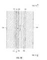
- FIGS. 1 A- 1 Care three different topological views of an interdigitated lateral power MOSFET in accordance with one embodiment of the present invention.
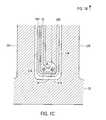
- FIG. 2is a cross-sectional side view taken through cut lines A-A′ in the embodiment of FIG. 1A.
- the field effect transistor of the present inventionincludes a metal gate electrode coupled with an insulated gate disposed over a channel region that separates elongated source and drain regions of the power MOSFET.
- the gatecomprises polysilicon
- the gate electrodeis coupled to the polysilicon gate using metal contacts (also known as vias) that are located at opposite ends of a portion of the insulated gate adjacent one side of the elongated source region.
- the source electrodeincludes two segments: a wide segment that carries most of the current flowing when the device is in the on state, and a narrow segment interposed between the drain electrode and the gate electrode that greatly reduces the drain-to-gate capacitance of the device.
- FIGS. 1 A- 1 Care a topological view of an interdigitated lateral power MOSFET in accordance with one embodiment of the present invention.
- FIG. 1Aprovides a view of the upper portion of the device
- FIG. 1Bis a view of the middle portion of the device
- FIG. 1Cshows the lower portion of the same transistor device.
- Each of these viewsillustrates a computer-aided design (CAD) layout of the drain, gate and source electrodes, the location of the polysilicon gate structure, and the placement of a select number of contacts or vias.
- CADcomputer-aided design
- FIGS. 1 A- 1 Cshould be viewed together with FIG. 2, which is a side view of the transistor taken through cut lines A-A′, for a more comprehensive understanding.
- FIG. 1Aillustrates the layout of the upper end of one embodiment of the interdigitated lateral power device of the present invention.
- the field-effect transistor of FIG. 1Aincludes an N-type source region 44 disposed in a semiconductor substrate and connected to a source electrode 21 by contacts (not shown in FIG. 1).
- Source electrode 21comprises source electrode segments 21 A and 21 B.
- Source region 44is interposed in the semiconductor substrate between two drain regions 42 , each of which is connected to a drain electrode 22 by contacts (see FIG. 2).
- Both of the source electrode segments 21 A & 21 Bare located between drain electrode segments 22 A and 22 B.
- FIG. 1Cshows the segments 22 A and 22 B merging into a single piece of metal at the bottom of the transistor. It is appreciated that the device layout structure of FIGS. 1 A- 1 C only shows a portion of the complete transistor in this embodiment.
- the full and complete devicecomprises a repeated pattern of the interdigitated source/drain/gate structures illustrated in the Figures. It is understood that since the drain and source structures are much longer than they are wide, they are often referred to as drain and source “fingers”.
- FIGS. 1 A- 1 CThe polysilicon material 28 that comprises the gate of the transistor is depicted in FIGS. 1 A- 1 C by dashed lines.
- the gateitself comprises two parallel members 28 A and 28 B disposed over channel region 49 , extending the length of the source finger.
- FIG. 1Cshows the polysilicon gate 28 wrapping around the far end, or fingertip, of the source region where the member 28 A merges with member 28 B.
- Members 28 A and 28 Bmany also be connected in the middle portion of the transistor, as shown in FIG. 1B.
- the polysilicon material of the gateextends under source electrode 21 and connects to metal line 29 through a plurality of contacts 30 .
- Metal line 29couples with control or switching circuitry used to drive the transistor.
- the two polysilicon gate members 28 A & 28 Bare insulated from the underlying semiconductor material by a gate dielectric layer 48 .
- Dielectric layermay comprise silicon dioxide, but other insulating materials, such as silicon nitride, may also be used.
- a portion of each member 28 A and 28 Bextends over a thicker field oxide layer 41 for field plating purposes.
- Each of the polysilicon gate members 28 A and 28 Bis covered with an interlayer dielectric 40 that insulates the gate from the overlying metal gate and source electrodes, as can be seen in the cross-sectional side view of FIG. 2.
- the gate electrode 25contacts one end of the polysilicon gate adjacent the base of the source finger through contact 31 , as shown in FIG. 1A.
- gate electroderuns lengthwise from one end of gate member 28 A to the opposite end adjacent the fingertip of the source region.
- FIG. 1Cshows gate electrode 25 being connected to the opposite end of gate member 28 A through a pair of contacts 34 . Note that gate electrode 25 ends adjacent the fingertip of the source and does not extend over gate member 28 B, which runs alongside the opposite side of source region 44 .
- connection of gate electrode 25 in parallel with insulated gate member 28 Aadvantageously distributes the applied gate signal along the length of each finger for improved high switching speed performance.
- one or more additional contactsmay be located at intermediate points or regions of the insulated gate between the opposite ends of the finger.
- FIG. 1Billustrates an optional additional contact 33 connecting gate electrode 25 to gate member 28 A at an intermediate point approximately halfway between the two ends of gate member 28 A.
- Gate member 28 Bmay also be connected to gate member 28 A in proximity to contact 33 to provide the same advantage in distribution of the gate signal along member 28 B.
- the width of the gate electrode 25 metalis made slightly wider to adequately surround contact 33 .
- source electrode segment 21 Bis made slightly narrower by a corresponding dimension. Note that no change in the width of source electrode segment 21 A (or drain electrodes 22 A & 22 B) is needed to accommodate the placement of additional contact 33 .
- the gate electrode 25is completely surrounded by source electrode 21 .
- the wider, current-carrying portion of the source electrodeis denoted as source electrode segment 21 B in FIGS. 1 A- 1 C.
- Segment 21 Bcarries the vast majority of the source current to the source bond pads (not shown) located at the upper end of the source finger.
- the source electrode segment 21 Balso includes a laterally extended portion that overlaps gate member 28 B. This laterally extended portion is located on the side of the finger opposite gate electrode 25 and functions as a field plate.
- the main source electrode segment 21 Bis disposed substantially over and contacts the substrate source region 44 .
- source electrode segment 21 AThe narrower portion of the source electrode is denoted as source electrode segment 21 A in FIGS. 1 A- 1 C.
- Source electrode segment 21 Ais interposed between gate electrode 25 and drain electrode 22 A.
- source electrode segment 21 Ahas no contacts to the underlying source diffusion, and does not carry a significant amount of source current. It functions as a source field plate and also reduces the drain-to-gate capacitance of the transistor. It should be understood that in other embodiments, source electrode segment 21 A may include contacts to the source diffusion region and/or may carry more significant amounts of source current.
- each of the source, drain, and gate electrodesare shown in FIGS. 1 & 2 as comprising a single layer of metal, alternative embodiments may utilize multiple levels of conductor material for each or all of the electrodes.
- FIG. 1Cillustrates source electrode segment 21 A wrapped around the source fingertip region of the transistor and connected to source electrode segment 21 B. It should be understood that the connection between segments 21 A and 21 B at this end of the source finger is optional. That is, these two segments need not connect at this point. However, source electrode segment 21 A should be connected to segment 21 B at some point in the layout so that both remain at substantially the same potential during device operation. This is consistent with the purpose of source segment 21 A to serve as a source field plate interposed between the gate electrode 25 and the drain electrode 22 .
- FIG. 2shows a cross-sectional view of the lateral power transistor of FIGS. 1 A- 1 C taken through cut lines A-A′.
- This diagramshows that drain electrode 22 A extends down through interlayer dielectric 40 to contact N+drain region 42 .
- Drain electrode 22 Aalso includes a field plate portion that extends laterally over interlayer dielectric 40 toward the source electrode segment 21 A.
- the distance between the drain electrode 22 A and the source electrode segment 21 Ais the same as the distance (e.g., 3 microns) between the gate electrode 25 and source electrode segment 21 A.
- the same distanceseparates the gate electrode 25 from the source electrode segment 21 B, which extends down to the surface of the substrate to contact N-type source region 44 and P+diffusion region 45 .
- This spacingis consistent with minimum design rules for an exemplary lateral power transistor having a 200V breakdown voltage.
- Drain diffusion region 42is disposed in N-well region 51 , which itself is a deep diffusion formed in P-substrate 60 .
- Source diffusion region 44is disposed in a P-well 50 formed adjacent to N-well 51 in substrate 60 .
- the channel region 49is defined between the boundaries of the N-well region 51 and source region 44 .
- the polysilicon gate members 28 A and 28 Bare formed over a thin gate oxide 48 above channel region 49 . Note that each of gate members 28 A and 28 B include field plating that extends over thicker field oxide layer 41 .
- the region between N+drain region 42 and channel 49is commonly referred to as the extended drain region of the device.
Landscapes
- Insulated Gate Type Field-Effect Transistor (AREA)
- Electrodes Of Semiconductors (AREA)
Abstract
Description
- The present invention relates to semiconductor devices fabricated in a silicon substrate. More specifically, the present invention relates to a high voltage field effect transistor with an improved gate design.[0001]
- A common type of integrated circuit device is a metal-oxide-semiconductor field effect transistor (MOSFET). A MOSFET is a field effect device that includes a source region, a drain region, a channel region extending between the source and drain regions, and a gate provided over the channel region. The gate includes a conductive gate structure disposed over and separated from the channel region with a thin oxide layer.[0002]
- Lateral field-effect transistors are widely used for high voltage circuit applications, e.g., greater than 200 volts. Examples of traditional lateral MOSFET device structures for power applications include U.S. Pat. Nos. 5,869,875, 5,821,144, 5,760,440, and 4,748,936. Each of these devices has a source region and a drain region separated by an intermediate region. A gate structure is disposed over a thin oxide layer over the metal-oxide-semiconductor (MOS) channel of the device. In the on state, a voltage is applied to the gate to cause a conduction channel to form between the source and drain regions, thereby allowing current to flow through the device. In the off state, the voltage on the gate is sufficiently low such that no conduction channel is formed in the substrate, and thus no current flow occurs. In this condition, high voltage is supported between the drain and source regions.[0003]
- Lateral power transistors are generally designed with source and drain regions that are elongated, or much longer than they are wide, and interdigitated. Such a device structure is disclosed in U.S. Pat. No. 6,084,277, which is assigned to the assignee of the present application. The '277 patent teaches a lateral power MOSFET or transistor having an improved gate design that provides a large safe operating area (SOA) performance level and high current capability with moderate gate speed to suppress switching noise. This is achieved by providing a metal gate electrode in parallel with the polysilicon gate structure along the length of the power MOSFET finger. The metal and polysilicon of the gate electrode and structure, respectively, are connected using metal contacts that are spaced apart along the gate structure. In one embodiment, the '277 patent teaches locating contacts at multiple locations between the gate electrode and gate structure along the power MOSFET finger to improve the propagation of the gate signal along the length of the finger for high switching speeds.[0004]
- One drawback associated with the lateral power transistor structure taught by the '277 patent is high gate-to-drain capacitance due to the proximate location of the gate and drain electrodes. The drain electrode serves as a drain field plate and the gate and/or source electrodes serve as source field plates to improve the breakdown voltage of these devices. Therefore, the extent and spacing of these electrodes is determined largely by breakdown voltage requirements. For instance, the '277 patent teaches an example device capable of sustaining 700 volts between the source and drain in the off state. Accordingly, this device includes a relatively large spacing between the drain and gate or source metal lines.[0005]
- But in the case where the device is designed for a much lower voltage, the closer spacing between the drain electrode and the gate electrode results in high gate-to-drain capacitance. A MOSFET designed with a breakdown voltage of 200 volts, for example, might have a spacing of less than 5 microns between the drain and gate electrode. Because these electrodes are commonly very long (e.g., 300-400 mm) the capacitance between the drain electrode and the gate or source electrode can be very large. This large capacitance degrades the high-speed switching performance of the transistor. High gate-to-drain capacitance is especially problematic because it is amplified by the gain of the transistor.[0006]
- Therefore, what is needed is a high voltage power transistor structure that achieves fast switching at high current conduction levels with good propagation of gate signal. Such a device should minimize drain-to-gate capacitance without increasing overall device size or cell pitch (i.e., silicon “footprint”).[0007]
- The present invention is illustrated by way of example, and not limitation, in the figures of the accompanying drawings, wherein:[0008]
- FIGS.[0009]1A-1C are three different topological views of an interdigitated lateral power MOSFET in accordance with one embodiment of the present invention.
- FIG. 2 is a cross-sectional side view taken through cut lines A-A′ in the embodiment of FIG. 1A.[0010]
- A high-voltage lateral power MOSFET with reduced gate-to-drain capacitance for high switching speeds is described. In the following description, numerous specific details are set forth, such as material types, dimensions, structural features, etc., in order to provide a thorough understanding of the present invention. Practitioners having ordinary skill in the semiconductor arts will understand that the invention may be practiced without many of these details. In other instances, well-known elements, techniques, and processing steps have not been described in detail to avoid obscuring the invention.[0011]
- The field effect transistor of the present invention includes a metal gate electrode coupled with an insulated gate disposed over a channel region that separates elongated source and drain regions of the power MOSFET. In one embodiment the gate comprises polysilicon, and the gate electrode is coupled to the polysilicon gate using metal contacts (also known as vias) that are located at opposite ends of a portion of the insulated gate adjacent one side of the elongated source region. The source electrode includes two segments: a wide segment that carries most of the current flowing when the device is in the on state, and a narrow segment interposed between the drain electrode and the gate electrode that greatly reduces the drain-to-gate capacitance of the device.[0012]
- FIGS.[0013]1A-1C are a topological view of an interdigitated lateral power MOSFET in accordance with one embodiment of the present invention. FIG. 1A provides a view of the upper portion of the device, FIG. 1B is a view of the middle portion of the device, and FIG. 1C shows the lower portion of the same transistor device. Each of these views illustrates a computer-aided design (CAD) layout of the drain, gate and source electrodes, the location of the polysilicon gate structure, and the placement of a select number of contacts or vias. It should be understood that the drain and source contacts are not shown and the underlying substrate diffusion regions are also omitted from FIGS.1A-1C in the interest of clarity. (During the following description, FIGS.1A-1C should be viewed together with FIG. 2, which is a side view of the transistor taken through cut lines A-A′, for a more comprehensive understanding.)
- FIG. 1A illustrates the layout of the upper end of one embodiment of the interdigitated lateral power device of the present invention. The field-effect transistor of FIG. 1A includes an N-[0014]
type source region 44 disposed in a semiconductor substrate and connected to asource electrode 21 by contacts (not shown in FIG. 1).Source electrode 21 comprisessource electrode segments Source region 44 is interposed in the semiconductor substrate between twodrain regions 42, each of which is connected to adrain electrode 22 by contacts (see FIG. 2). - Both of the[0015]
source electrode segments 21A &21B are located betweendrain electrode segments segments - The[0016]
polysilicon material 28 that comprises the gate of the transistor is depicted in FIGS.1A-1C by dashed lines. The gate itself comprises twoparallel members channel region 49, extending the length of the source finger. FIG. 1C shows thepolysilicon gate 28 wrapping around the far end, or fingertip, of the source region where themember 28A merges withmember 28B.Members - At the upper end of the transistor, the polysilicon material of the gate extends under[0017]
source electrode 21 and connects tometal line 29 through a plurality ofcontacts 30.Metal line 29 couples with control or switching circuitry used to drive the transistor. - As shown in FIG. 2, the two[0018]
polysilicon gate members 28A &28B are insulated from the underlying semiconductor material by agate dielectric layer 48. Dielectric layer may comprise silicon dioxide, but other insulating materials, such as silicon nitride, may also be used. A portion of eachmember field oxide layer 41 for field plating purposes. Each of thepolysilicon gate members interlayer dielectric 40 that insulates the gate from the overlying metal gate and source electrodes, as can be seen in the cross-sectional side view of FIG. 2. - The[0019]
gate electrode 25 contacts one end of the polysilicon gate adjacent the base of the source finger through contact31, as shown in FIG. 1A. In the illustrated embodiment, gate electrode runs lengthwise from one end ofgate member 28A to the opposite end adjacent the fingertip of the source region. FIG. 1C showsgate electrode 25 being connected to the opposite end ofgate member 28A through a pair ofcontacts 34. Note thatgate electrode 25 ends adjacent the fingertip of the source and does not extend overgate member 28B, which runs alongside the opposite side ofsource region 44. - It is appreciated that the connection of[0020]
gate electrode 25 in parallel withinsulated gate member 28A advantageously distributes the applied gate signal along the length of each finger for improved high switching speed performance. Depending on the length of the source, drain, and gate fingers, one or more additional contacts may be located at intermediate points or regions of the insulated gate between the opposite ends of the finger. For example, FIG. 1B illustrates an optionaladditional contact 33 connectinggate electrode 25 togate member 28A at an intermediate point approximately halfway between the two ends ofgate member 28A.Gate member 28B may also be connected togate member 28A in proximity to contact33 to provide the same advantage in distribution of the gate signal alongmember 28B. - To accommodate the placement of[0021]
contact 33 the width of thegate electrode 25 metal is made slightly wider to adequately surroundcontact 33. To maintain design rule separation between the source and gate electrodes,source electrode segment 21B is made slightly narrower by a corresponding dimension. Note that no change in the width ofsource electrode segment 21A (ordrain electrodes 22A &22B) is needed to accommodate the placement ofadditional contact 33. - The[0022]
gate electrode 25 is completely surrounded bysource electrode 21. The wider, current-carrying portion of the source electrode is denoted assource electrode segment 21B in FIGS.1A-1C.Segment 21B carries the vast majority of the source current to the source bond pads (not shown) located at the upper end of the source finger. Thesource electrode segment 21B also includes a laterally extended portion that overlapsgate member 28B. This laterally extended portion is located on the side of the finger oppositegate electrode 25 and functions as a field plate. The mainsource electrode segment 21B is disposed substantially over and contacts thesubstrate source region 44. - The narrower portion of the source electrode is denoted as[0023]
source electrode segment 21A in FIGS.1A-1C.Source electrode segment 21A is interposed betweengate electrode 25 anddrain electrode 22A. In the embodiment of FIGS.1A-1C,source electrode segment 21A has no contacts to the underlying source diffusion, and does not carry a significant amount of source current. It functions as a source field plate and also reduces the drain-to-gate capacitance of the transistor. It should be understood that in other embodiments,source electrode segment 21A may include contacts to the source diffusion region and/or may carry more significant amounts of source current. - In addition, although each of the source, drain, and gate electrodes are shown in FIGS. 1 & 2 as comprising a single layer of metal, alternative embodiments may utilize multiple levels of conductor material for each or all of the electrodes.[0024]
- FIG. 1C illustrates[0025]
source electrode segment 21A wrapped around the source fingertip region of the transistor and connected to sourceelectrode segment 21B. It should be understood that the connection betweensegments source electrode segment 21A should be connected tosegment 21B at some point in the layout so that both remain at substantially the same potential during device operation. This is consistent with the purpose ofsource segment 21A to serve as a source field plate interposed between thegate electrode 25 and thedrain electrode 22. - FIG. 2 shows a cross-sectional view of the lateral power transistor of FIGS.[0026]1A-1C taken through cut lines A-A′. This diagram shows that
drain electrode 22A extends down throughinterlayer dielectric 40 to contact N+drain region 42.Drain electrode 22A also includes a field plate portion that extends laterally overinterlayer dielectric 40 toward thesource electrode segment 21A. In the illustrated embodiment, the distance between thedrain electrode 22A and thesource electrode segment 21A is the same as the distance (e.g., 3 microns) between thegate electrode 25 andsource electrode segment 21A. The same distance separates thegate electrode 25 from thesource electrode segment 21B, which extends down to the surface of the substrate to contact N-type source region 44 and P+diffusion region 45. This spacing is consistent with minimum design rules for an exemplary lateral power transistor having a 200V breakdown voltage. - [0027]
Drain diffusion region 42 is disposed in N-well region 51, which itself is a deep diffusion formed in P-substrate 60.Source diffusion region 44 is disposed in a P-well50 formed adjacent to N-well51 insubstrate 60. Thechannel region 49 is defined between the boundaries of the N-well region 51 andsource region 44. Thepolysilicon gate members thin gate oxide 48 abovechannel region 49. Note that each ofgate members field oxide layer 41. The region between N+drain region 42 andchannel 49 is commonly referred to as the extended drain region of the device. - It is appreciated that the foregoing details of the various regions formed in the semiconductor material beneath the top surface of the substrate are specific to the embodiment shown and are not deemed essential to the present invention. In other words, the layout structure of the metal electrodes and gate members may be utilized in transistors having different doped semiconductor regions of the device.[0028]
Claims (30)
1. A field-effect transistor comprising:
elongated source and drain regions separated by a channel region;
an insulated gate disposed over the channel region;
a drain electrode coupled to the drain region;
a gate electrode coupled to the insulated gate through first and second contacts located at respective first and second contact regions of the insulated gate, the first and second regions being separated by a contact-free region; and
a source electrode coupled to the source region, the source electrode including first and second segments, the first segment being interposed between the drain electrode and the gate electrode.
2. The field-effect transistor according toclaim 1 wherein the second segment of the source electrode is disposed substantially over the source region.
3. The field-effect transistor according toclaim 2 wherein the drain electrode is disposed substantially over the drain region.
4. The field-effect transistor according toclaim 3 wherein the source and drain electrodes each include a field plate portion.
5. The field-effect transistor according toclaim 1 wherein the first and second segments are disposed on opposite sides of the gate electrode.
6. The field-effect transistor according toclaim 1 wherein the first and second segments surround the gate electrode.
7. The field-effect transistor according toclaim 1 wherein the second segment is wider than the first segment.
8. The field-effect transistor according toclaim 1 wherein the source and drain regions are interdigitated.
9. The field-effect transistor according toclaim 1 wherein the insulated gate has a first end and second end opposite the first end, the first contact region being located at the first end and the second contact region being located at the second end.
10. The field-effect transistor according toclaim 1 wherein the insulated gate has a first end and second end opposite the first end, the first contact region being located at the first end and the second contact region being located at an intermediate point between the first and second ends, and wherein the gate electrode is further coupled to the insulated gate through a third contact located at a third contact region of the insulated gate, the third contact region being located at the second end.
11. A lateral field-effect transistor comprising:
elongated source and drain regions separated by a channel region;
an insulated gate disposed over the channel region, the insulated gate having a first end region and a second end region opposite the first end region;
a drain electrode coupled to the drain region;
a gate electrode coupled to the insulated gate through first and second contacts located at the first and second end regions of the insulated gate, respectively; and
a source electrode coupled to the source region, the source electrode including first and second segments, the first segment being interposed between the drain electrode and the gate electrode.
12. The lateral field-effect transistor according toclaim 11 wherein the second segment of the source electrode is disposed substantially over the source region.
13. The lateral field-effect transistor according toclaim 12 wherein the drain electrode is disposed substantially over the drain region.
14. The lateral field-effect transistor according toclaim 11 wherein the source and drain electrodes each include a field plate portion.
15. The lateral field-effect transistor according toclaim 11 wherein the first and second segments are disposed on opposite sides of the gate electrode.
16. The lateral field-effect transistor according toclaim 11 wherein the first and second segments surround the gate electrode.
17. The lateral field-effect transistor according toclaim 11 wherein the second segment is wider than the first segment.
18. The lateral field-effect transistor according toclaim 11 wherein the source and drain regions are interdigitated.
19. The lateral field-effect transistor according toclaim 11 wherein the first segment of the source electrode is spaced equidistant from the gate and drain electrodes.
20. The lateral field-effect transistor according toclaim 11 wherein the insulated gate has an intermediate region between the first and second end regions, and wherein the gate electrode is further coupled to the insulated gate through a third contact located at the intermediate region.
21. A lateral power MOSFET comprising:
an elongated source region interdigitated between a pair of drain regions, the source region being separated from the pair of drain regions by a channel region, the elongated source region having a first and second ends;
an insulated gate disposed over the channel region, the insulated gate having a first portion that extends from adjacent the first end to adjacent the second end along one side of the elongated source region and a second portion that extends from adjacent the first end to adjacent the second end along an opposite side of the elongated source region;
a drain electrode coupled to the drain region;
a gate electrode coupled to the insulated gate through first and second contacts located at opposite ends of the first portion of the insulated gate; and
a source electrode coupled to the elongated source region, the source electrode including first and second elongated segments, the first elongated segment being interposed between the drain electrode and the gate electrode.
22. The lateral power MOSFET according toclaim 21 wherein the second segment of the source electrode is disposed substantially over the source region.
23. The lateral power MOSFET according toclaim 21 wherein the drain electrode is disposed substantially over the drain region.
24. The lateral power MOSFET according toclaim 21 wherein the source and drain electrodes each include a field plate portion.
25. The lateral power MOSFET according toclaim 21 wherein the first and second elongated segments are disposed on opposite sides of the gate electrode.
26. The lateral power MOSFET according toclaim 21 wherein the first and second elongated segments surround the gate electrode.
27. The lateral power MOSFET according toclaim 21 wherein the second elongated segment is wider than the first elongated segment.
28. The lateral power MOSFET according toclaim 21 wherein each of the pair of drain regions is elongated.
29. The lateral power MOSFET according toclaim 21 wherein the first segment of the source electrode is spaced equidistant from the gate and drain electrodes.
30. The lateral power MOSFET according toclaim 21 wherein the first portion of the insulated gate has an intermediate region between the opposite ends, and wherein the gate electrode is further coupled to the insulated gate through a third contact located at the intermediate region.
Priority Applications (9)
| Application Number | Priority Date | Filing Date | Title |
|---|---|---|---|
| US10/016,748US6555883B1 (en) | 2001-10-29 | 2001-10-29 | Lateral power MOSFET for high switching speeds |
| JP2002258265AJP4879444B2 (en) | 2001-10-29 | 2002-07-31 | Lateral power MOSFET for high switching speed |
| AT02255740TATE515802T1 (en) | 2001-10-29 | 2002-08-16 | LATERAL POWER MOSFET |
| EP02255740AEP1306905B1 (en) | 2001-10-29 | 2002-08-16 | Lateral power MOSFET |
| EP05000643.6AEP1530240B1 (en) | 2001-10-29 | 2002-08-16 | Lateral insulated gate field-effet transistor |
| US10/340,040US6825536B2 (en) | 2001-10-29 | 2003-01-10 | Lateral power MOSFET for high switching speeds |
| JP2004179762AJP4689977B2 (en) | 2001-10-29 | 2004-06-17 | Lateral power MOSFET for high switching speed |
| US10/968,659US7115958B2 (en) | 2001-10-29 | 2004-10-19 | Lateral power MOSFET for high switching speeds |
| JP2010099572AJP5306277B2 (en) | 2001-10-29 | 2010-04-23 | Lateral power MOSFET for high switching speed |
Applications Claiming Priority (1)
| Application Number | Priority Date | Filing Date | Title |
|---|---|---|---|
| US10/016,748US6555883B1 (en) | 2001-10-29 | 2001-10-29 | Lateral power MOSFET for high switching speeds |
Related Child Applications (1)
| Application Number | Title | Priority Date | Filing Date |
|---|---|---|---|
| US10/340,040ContinuationUS6825536B2 (en) | 2001-10-29 | 2003-01-10 | Lateral power MOSFET for high switching speeds |
Publications (2)
| Publication Number | Publication Date |
|---|---|
| US6555883B1 US6555883B1 (en) | 2003-04-29 |
| US20030080388A1true US20030080388A1 (en) | 2003-05-01 |
Family
ID=21778744
Family Applications (3)
| Application Number | Title | Priority Date | Filing Date |
|---|---|---|---|
| US10/016,748Expired - LifetimeUS6555883B1 (en) | 2001-10-29 | 2001-10-29 | Lateral power MOSFET for high switching speeds |
| US10/340,040Expired - Fee RelatedUS6825536B2 (en) | 2001-10-29 | 2003-01-10 | Lateral power MOSFET for high switching speeds |
| US10/968,659Expired - Fee RelatedUS7115958B2 (en) | 2001-10-29 | 2004-10-19 | Lateral power MOSFET for high switching speeds |
Family Applications After (2)
| Application Number | Title | Priority Date | Filing Date |
|---|---|---|---|
| US10/340,040Expired - Fee RelatedUS6825536B2 (en) | 2001-10-29 | 2003-01-10 | Lateral power MOSFET for high switching speeds |
| US10/968,659Expired - Fee RelatedUS7115958B2 (en) | 2001-10-29 | 2004-10-19 | Lateral power MOSFET for high switching speeds |
Country Status (4)
| Country | Link |
|---|---|
| US (3) | US6555883B1 (en) |
| EP (2) | EP1306905B1 (en) |
| JP (3) | JP4879444B2 (en) |
| AT (1) | ATE515802T1 (en) |
Cited By (10)
| Publication number | Priority date | Publication date | Assignee | Title |
|---|---|---|---|---|
| US20050082522A1 (en)* | 2003-07-25 | 2005-04-21 | Yi-Chun Huang | Strained channel transistor formation |
| US20060017105A1 (en)* | 2004-07-22 | 2006-01-26 | Matsushita Electric Industrial Co., Ltd. | Semiconductor device and method of fabricating the same |
| US7029994B2 (en) | 2003-04-03 | 2006-04-18 | Taiwan Semiconductor Manufacturing Company, Ltd. | Strained channel on insulator device |
| US20060124965A1 (en)* | 2003-07-25 | 2006-06-15 | Yee-Chia Yeo | Capacitor that includes high permittivity capacitor dielectric |
| US20060226487A1 (en)* | 2003-08-18 | 2006-10-12 | Yee-Chia Yeo | Resistor with reduced leakage |
| US20060255365A1 (en)* | 2003-08-15 | 2006-11-16 | Chih-Hsin Ko | Structure and method of a strained channel transistor and a second semiconductor component in an integrated circuit |
| US20080169484A1 (en)* | 2007-01-16 | 2008-07-17 | Harry Chuang | Strained Transistor with Optimized Drive Current and Method of Forming |
| US20090230439A1 (en)* | 2008-03-13 | 2009-09-17 | Yen-Sen Wang | Strain Bars in Stressed Layers of MOS Devices |
| US20100078725A1 (en)* | 2008-09-29 | 2010-04-01 | Yung-Chin Hou | Standard Cell without OD Space Effect in Y-Direction |
| US7888201B2 (en) | 2003-11-04 | 2011-02-15 | Taiwan Semiconductor Manufacturing Company, Ltd. | Semiconductor-on-insulator SRAM configured using partially-depleted and fully-depleted transistors |
Families Citing this family (51)
| Publication number | Priority date | Publication date | Assignee | Title |
|---|---|---|---|---|
| US7221011B2 (en) | 2001-09-07 | 2007-05-22 | Power Integrations, Inc. | High-voltage vertical transistor with a multi-gradient drain doping profile |
| US6573558B2 (en) | 2001-09-07 | 2003-06-03 | Power Integrations, Inc. | High-voltage vertical transistor with a multi-layered extended drain structure |
| US7786533B2 (en)* | 2001-09-07 | 2010-08-31 | Power Integrations, Inc. | High-voltage vertical transistor with edge termination structure |
| US6635544B2 (en)* | 2001-09-07 | 2003-10-21 | Power Intergrations, Inc. | Method of fabricating a high-voltage transistor with a multi-layered extended drain structure |
| US6555883B1 (en)* | 2001-10-29 | 2003-04-29 | Power Integrations, Inc. | Lateral power MOSFET for high switching speeds |
| EP1408552A1 (en)* | 2002-10-09 | 2004-04-14 | STMicroelectronics S.r.l. | Integrated MOS semiconductor device with high performance and process of manufacturing the same |
| US6933562B1 (en) | 2003-06-27 | 2005-08-23 | National Semiconductor Corporation | Power transistor structure with non-uniform metal widths |
| EP1501130A1 (en)* | 2003-07-21 | 2005-01-26 | STMicroelectronics S.r.l. | Semiconductor MOS device and related manufacturing method |
| US6982461B2 (en)* | 2003-12-08 | 2006-01-03 | Semiconductor Components Industries, L.L.C. | Lateral FET structure with improved blocking voltage and on resistance performance and method |
| US8264039B2 (en)* | 2004-04-26 | 2012-09-11 | Synopsys, Inc. | High-voltage LDMOSFET and applications therefor in standard CMOS |
| US7375398B2 (en)* | 2004-07-02 | 2008-05-20 | Impinj, Inc. | High voltage FET gate structure |
| US8159001B2 (en)* | 2004-07-02 | 2012-04-17 | Synopsys, Inc. | Graded junction high voltage semiconductor device |
| US7265399B2 (en) | 2004-10-29 | 2007-09-04 | Cree, Inc. | Asymetric layout structures for transistors and methods of fabricating the same |
| US20060223293A1 (en)* | 2005-04-01 | 2006-10-05 | Raytheon Company | Semiconductor devices having improved field plates |
| US7989879B2 (en)* | 2005-07-13 | 2011-08-02 | Nxp B.V. | LDMOS transistor |
| US8093621B2 (en)* | 2008-12-23 | 2012-01-10 | Power Integrations, Inc. | VTS insulated gate bipolar transistor |
| US7468536B2 (en) | 2007-02-16 | 2008-12-23 | Power Integrations, Inc. | Gate metal routing for transistor with checkerboarded layout |
| US7859037B2 (en) | 2007-02-16 | 2010-12-28 | Power Integrations, Inc. | Checkerboarded high-voltage vertical transistor layout |
| US8653583B2 (en)* | 2007-02-16 | 2014-02-18 | Power Integrations, Inc. | Sensing FET integrated with a high-voltage transistor |
| US7557406B2 (en)* | 2007-02-16 | 2009-07-07 | Power Integrations, Inc. | Segmented pillar layout for a high-voltage vertical transistor |
| US7595523B2 (en) | 2007-02-16 | 2009-09-29 | Power Integrations, Inc. | Gate pullback at ends of high-voltage vertical transistor structure |
| US7875962B2 (en)* | 2007-10-15 | 2011-01-25 | Power Integrations, Inc. | Package for a power semiconductor device |
| US7701065B2 (en)* | 2007-10-26 | 2010-04-20 | Infineon Technologies Ag | Device including a semiconductor chip having a plurality of electrodes |
| US7964912B2 (en) | 2008-09-18 | 2011-06-21 | Power Integrations, Inc. | High-voltage vertical transistor with a varied width silicon pillar |
| JP5304195B2 (en)* | 2008-11-20 | 2013-10-02 | 株式会社デンソー | Semiconductor device |
| US7871882B2 (en) | 2008-12-20 | 2011-01-18 | Power Integrations, Inc. | Method of fabricating a deep trench insulated gate bipolar transistor |
| US20100155831A1 (en)* | 2008-12-20 | 2010-06-24 | Power Integrations, Inc. | Deep trench insulated gate bipolar transistor |
| TWI404207B (en)* | 2008-12-26 | 2013-08-01 | Vanguard Int Semiconduct Corp | Semiconductor structure |
| US7875930B2 (en)* | 2009-02-16 | 2011-01-25 | Vanguard International Semiconductor Corporation | Semiconductor structure having an enlarged finger shaped region for reducing electric field density and method of manufacturing the same |
| JP5525736B2 (en)* | 2009-02-18 | 2014-06-18 | セミコンダクター・コンポーネンツ・インダストリーズ・リミテッド・ライアビリティ・カンパニー | Semiconductor device and manufacturing method thereof |
| US8207455B2 (en)* | 2009-07-31 | 2012-06-26 | Power Integrations, Inc. | Power semiconductor package with bottom surface protrusions |
| US8115457B2 (en) | 2009-07-31 | 2012-02-14 | Power Integrations, Inc. | Method and apparatus for implementing a power converter input terminal voltage discharge circuit |
| US8207577B2 (en)* | 2009-09-29 | 2012-06-26 | Power Integrations, Inc. | High-voltage transistor structure with reduced gate capacitance |
| US7893754B1 (en) | 2009-10-02 | 2011-02-22 | Power Integrations, Inc. | Temperature independent reference circuit |
| US8634218B2 (en)* | 2009-10-06 | 2014-01-21 | Power Integrations, Inc. | Monolithic AC/DC converter for generating DC supply voltage |
| US8310845B2 (en)* | 2010-02-10 | 2012-11-13 | Power Integrations, Inc. | Power supply circuit with a control terminal for different functional modes of operation |
| US9583478B1 (en) | 2010-04-16 | 2017-02-28 | Silego Technology, Inc. | Lateral power MOSFET |
| US8350338B2 (en) | 2011-02-08 | 2013-01-08 | International Business Machines Corporations | Semiconductor device including high field regions and related method |
| TWI584476B (en)* | 2011-08-25 | 2017-05-21 | 聯華電子股份有限公司 | High voltage metal-oxide-semiconductor transistor device and method of fabricating the same |
| US8653600B2 (en) | 2012-06-01 | 2014-02-18 | Power Integrations, Inc. | High-voltage monolithic schottky device structure |
| US9455621B2 (en) | 2013-08-28 | 2016-09-27 | Power Integrations, Inc. | Controller IC with zero-crossing detector and capacitor discharge switching element |
| JP6252122B2 (en)* | 2013-11-13 | 2017-12-27 | 富士通株式会社 | Semiconductor device and manufacturing method of semiconductor device |
| US9543396B2 (en) | 2013-12-13 | 2017-01-10 | Power Integrations, Inc. | Vertical transistor device structure with cylindrically-shaped regions |
| US10325988B2 (en) | 2013-12-13 | 2019-06-18 | Power Integrations, Inc. | Vertical transistor device structure with cylindrically-shaped field plates |
| DE102014111140B4 (en)* | 2014-08-05 | 2019-08-14 | Infineon Technologies Austria Ag | Semiconductor device with field effect structures with different gate materials and method for the production thereof |
| US9667154B2 (en) | 2015-09-18 | 2017-05-30 | Power Integrations, Inc. | Demand-controlled, low standby power linear shunt regulator |
| US9602009B1 (en) | 2015-12-08 | 2017-03-21 | Power Integrations, Inc. | Low voltage, closed loop controlled energy storage circuit |
| US9629218B1 (en) | 2015-12-28 | 2017-04-18 | Power Integrations, Inc. | Thermal protection for LED bleeder in fault condition |
| CN105742364A (en)* | 2016-04-12 | 2016-07-06 | 中山大学 | MOS transistor capable of restraining photoinduced leakage current in active channel region, and application of MOS transistor |
| US10930737B2 (en) | 2016-11-24 | 2021-02-23 | Visic Technologies Ltd. | Transistor cell |
| DE102017130213B4 (en)* | 2017-12-15 | 2021-10-21 | Infineon Technologies Ag | PLANAR FIELD EFFECT TRANSISTOR |
Family Cites Families (69)
| Publication number | Priority date | Publication date | Assignee | Title |
|---|---|---|---|---|
| JPS5638867A (en) | 1979-09-07 | 1981-04-14 | Hitachi Ltd | Insulated gate type field effect transistor |
| JPS5712558A (en) | 1980-06-25 | 1982-01-22 | Sanyo Electric Co Ltd | Mos transistor having high withstand voltage |
| JPS5712557A (en) | 1980-06-25 | 1982-01-22 | Sanyo Electric Co Ltd | High dielectric resisting mos transistor |
| JPS5710975A (en) | 1980-06-25 | 1982-01-20 | Sanyo Electric Co Ltd | High dielectric strength high transistor |
| US4738936A (en) | 1983-07-01 | 1988-04-19 | Acrian, Inc. | Method of fabrication lateral FET structure having a substrate to source contact |
| JPS6064471A (en) | 1983-09-19 | 1985-04-13 | Nec Corp | High voltage insulated gate field effect transistor |
| JPS61168253A (en) | 1985-01-19 | 1986-07-29 | Sharp Corp | High withstand voltage mos field effect semiconductor device |
| JPS63229857A (en)* | 1987-03-19 | 1988-09-26 | Sanyo Electric Co Ltd | Protective circuit against electrostatic breakdown |
| JPS63260220A (en)* | 1987-04-16 | 1988-10-27 | Oi Denki Kk | Rush current preventing circuit |
| JPH02250378A (en)* | 1989-03-24 | 1990-10-08 | Hitachi Ltd | Semiconductor device |
| US5100821A (en)* | 1989-04-24 | 1992-03-31 | Motorola, Inc. | Semiconductor AC switch |
| JP2877408B2 (en) | 1990-01-12 | 1999-03-31 | 株式会社東芝 | Conduction modulation type MOSFET |
| SG48388A1 (en)* | 1990-02-01 | 1998-04-17 | Fred L Quigg | Mosfet structure having reduced gate capacitance and method of forming same |
| JP2991753B2 (en) | 1990-08-27 | 1999-12-20 | 松下電子工業株式会社 | Semiconductor device and manufacturing method thereof |
| JP3158738B2 (en) | 1992-08-17 | 2001-04-23 | 富士電機株式会社 | High breakdown voltage MIS field-effect transistor and semiconductor integrated circuit |
| JPH06151846A (en)* | 1992-11-04 | 1994-05-31 | Toshiba Corp | Semiconductor device |
| US5326711A (en) | 1993-01-04 | 1994-07-05 | Texas Instruments Incorporated | High performance high voltage vertical transistor and method of fabrication |
| JP3076468B2 (en) | 1993-01-26 | 2000-08-14 | 松下電子工業株式会社 | Semiconductor device |
| DE4309764C2 (en) | 1993-03-25 | 1997-01-30 | Siemens Ag | Power MOSFET |
| JPH06310955A (en)* | 1993-04-22 | 1994-11-04 | Fujitsu Ltd | High output field effect transistor |
| JP3173268B2 (en)* | 1994-01-06 | 2001-06-04 | 富士電機株式会社 | Semiconductor device having MIS field-effect transistor |
| JP3136885B2 (en)* | 1994-02-02 | 2001-02-19 | 日産自動車株式会社 | Power MOSFET |
| US5767546A (en)* | 1994-12-30 | 1998-06-16 | Siliconix Incorporated | Laternal power mosfet having metal strap layer to reduce distributed resistance |
| US5689209A (en)* | 1994-12-30 | 1997-11-18 | Siliconix Incorporated | Low-side bidirectional battery disconnect switch |
| JP3291958B2 (en) | 1995-02-21 | 2002-06-17 | 富士電機株式会社 | Back source MOSFET |
| KR0167273B1 (en)* | 1995-12-02 | 1998-12-15 | 문정환 | High voltage mosfet device and manufacturing method thereof |
| JPH09266311A (en) | 1996-01-22 | 1997-10-07 | Fuji Electric Co Ltd | Semiconductor device and manufacturing method thereof |
| US6097063A (en) | 1996-01-22 | 2000-08-01 | Fuji Electric Co., Ltd. | Semiconductor device having a plurality of parallel drift regions |
| DE19611045C1 (en) | 1996-03-20 | 1997-05-22 | Siemens Ag | Field effect transistor e.g. vertical MOS type |
| JP3327135B2 (en)* | 1996-09-09 | 2002-09-24 | 日産自動車株式会社 | Field effect transistor |
| US5841166A (en) | 1996-09-10 | 1998-11-24 | Spectrian, Inc. | Lateral DMOS transistor for RF/microwave applications |
| US5977569A (en)* | 1996-09-24 | 1999-11-02 | Allen-Bradley Company, Llc | Bidirectional lateral insulated gate bipolar transistor having increased voltage blocking capability |
| WO1998049732A2 (en) | 1997-04-28 | 1998-11-05 | Koninklijke Philips Electronics N.V. | Lateral mos transistor device |
| EP0922302A2 (en)* | 1997-05-23 | 1999-06-16 | Koninklijke Philips Electronics N.V. | Lateral mos transistor device |
| US5869875A (en) | 1997-06-10 | 1999-02-09 | Spectrian | Lateral diffused MOS transistor with trench source contact |
| US6054752A (en) | 1997-06-30 | 2000-04-25 | Denso Corporation | Semiconductor device |
| US5898198A (en)* | 1997-08-04 | 1999-04-27 | Spectrian | RF power device having voltage controlled linearity |
| EP0965145B1 (en) | 1997-12-24 | 2011-09-21 | Nxp B.V. | A high voltage thin film transistor with improved on-state characteristics and method for making same |
| JP3641547B2 (en)* | 1998-03-25 | 2005-04-20 | 株式会社豊田中央研究所 | Semiconductor device including lateral MOS element |
| DE69839439D1 (en)* | 1998-05-26 | 2008-06-19 | St Microelectronics Srl | MOS technology power arrangement with high integration density |
| JP3016762B2 (en) | 1998-06-25 | 2000-03-06 | 松下電子工業株式会社 | Semiconductor device and manufacturing method thereof |
| DE19854915C2 (en) | 1998-11-27 | 2002-09-05 | Infineon Technologies Ag | MOS field effect transistor with auxiliary electrode |
| US6084277A (en)* | 1999-02-18 | 2000-07-04 | Power Integrations, Inc. | Lateral power MOSFET with improved gate design |
| JP2002541668A (en)* | 1999-03-31 | 2002-12-03 | サイスド エレクトロニクス デヴェロプメント ゲゼルシャフト ミット ベシュレンクテル ハフツング ウント コンパニ コマンディートゲゼルシャフト | Integrated semiconductor device having a lateral power element |
| WO2000075989A1 (en)* | 1999-06-03 | 2000-12-14 | Koninklijke Philips Electronics N.V. | Semiconductor device comprising a high-voltage circuit element |
| KR100302611B1 (en)* | 1999-06-07 | 2001-10-29 | 김영환 | High power semiconductor device and fabrication method thereof |
| GB9917099D0 (en) | 1999-07-22 | 1999-09-22 | Koninkl Philips Electronics Nv | Cellular trench-gate field-effect transistors |
| JP3971062B2 (en) | 1999-07-29 | 2007-09-05 | 株式会社東芝 | High voltage semiconductor device |
| US6365932B1 (en)* | 1999-08-20 | 2002-04-02 | Denso Corporation | Power MOS transistor |
| JP2001102569A (en)* | 1999-09-28 | 2001-04-13 | Fuji Electric Co Ltd | Semiconductor device |
| US6489653B2 (en)* | 1999-12-27 | 2002-12-03 | Kabushiki Kaisha Toshiba | Lateral high-breakdown-voltage transistor |
| JP2001274390A (en)* | 2000-01-18 | 2001-10-05 | Fuji Electric Co Ltd | High breakdown voltage device, manufacturing method thereof, and method of forming impurity diffusion region |
| JP3356152B2 (en)* | 2000-02-23 | 2002-12-09 | 日本電気株式会社 | Semiconductor device |
| US6617642B1 (en)* | 2000-02-23 | 2003-09-09 | Tripath Technology, Inc. | Field effect transistor structure for driving inductive loads |
| JP2001352070A (en)* | 2000-04-07 | 2001-12-21 | Denso Corp | Semiconductor device and method of manufacturing the same |
| US6492678B1 (en)* | 2000-05-03 | 2002-12-10 | Linear Technology Corporation | High voltage MOS transistor with gate extension |
| US6525390B2 (en)* | 2000-05-18 | 2003-02-25 | Fuji Electric Co., Ltd. | MIS semiconductor device with low on resistance and high breakdown voltage |
| US20020071293A1 (en)* | 2000-07-13 | 2002-06-13 | Eden Richard C. | Power semiconductor switching devices, power converters, integrated circuit assemblies, integrated circuitry, power current switching methods, methods of forming a power semiconductor switching device, power conversion methods, power semiconductor switching device packaging methods, and methods a of forming power transistor |
| JP3448015B2 (en) | 2000-07-26 | 2003-09-16 | 松下電器産業株式会社 | Semiconductor device and manufacturing method thereof |
| AU2002230482A1 (en) | 2000-11-16 | 2002-05-27 | Silicon Wireless Corporation | Discrete and packaged power devices for radio frequency (rf) applications and methods of forming same |
| US6644617B2 (en)* | 2000-12-06 | 2003-11-11 | Nelson Douglas Pitlor | Remotely attachable and separable coupling |
| US6445052B1 (en)* | 2001-01-05 | 2002-09-03 | United Microelectronics Corp. | Power lateral diffused MOS transistor |
| US6677641B2 (en) | 2001-10-17 | 2004-01-13 | Fairchild Semiconductor Corporation | Semiconductor structure with improved smaller forward voltage loss and higher blocking capability |
| US6683346B2 (en) | 2001-03-09 | 2004-01-27 | Fairchild Semiconductor Corporation | Ultra dense trench-gated power-device with the reduced drain-source feedback capacitance and Miller charge |
| US6853033B2 (en) | 2001-06-05 | 2005-02-08 | National University Of Singapore | Power MOSFET having enhanced breakdown voltage |
| JP4421144B2 (en) | 2001-06-29 | 2010-02-24 | 株式会社東芝 | Semiconductor device |
| US6555873B2 (en) | 2001-09-07 | 2003-04-29 | Power Integrations, Inc. | High-voltage lateral transistor with a multi-layered extended drain structure |
| US6555883B1 (en)* | 2001-10-29 | 2003-04-29 | Power Integrations, Inc. | Lateral power MOSFET for high switching speeds |
| US6865093B2 (en) | 2003-05-27 | 2005-03-08 | Power Integrations, Inc. | Electronic circuit control element with tap element |
- 2001
- 2001-10-29USUS10/016,748patent/US6555883B1/ennot_activeExpired - Lifetime
- 2002
- 2002-07-31JPJP2002258265Apatent/JP4879444B2/ennot_activeExpired - Fee Related
- 2002-08-16ATAT02255740Tpatent/ATE515802T1/ennot_activeIP Right Cessation
- 2002-08-16EPEP02255740Apatent/EP1306905B1/ennot_activeExpired - Lifetime
- 2002-08-16EPEP05000643.6Apatent/EP1530240B1/ennot_activeExpired - Lifetime
- 2003
- 2003-01-10USUS10/340,040patent/US6825536B2/ennot_activeExpired - Fee Related
- 2004
- 2004-06-17JPJP2004179762Apatent/JP4689977B2/ennot_activeExpired - Fee Related
- 2004-10-19USUS10/968,659patent/US7115958B2/ennot_activeExpired - Fee Related
- 2010
- 2010-04-23JPJP2010099572Apatent/JP5306277B2/ennot_activeExpired - Fee Related
Cited By (19)
| Publication number | Priority date | Publication date | Assignee | Title |
|---|---|---|---|---|
| US7029994B2 (en) | 2003-04-03 | 2006-04-18 | Taiwan Semiconductor Manufacturing Company, Ltd. | Strained channel on insulator device |
| US20050082522A1 (en)* | 2003-07-25 | 2005-04-21 | Yi-Chun Huang | Strained channel transistor formation |
| US7745279B2 (en) | 2003-07-25 | 2010-06-29 | Taiwan Semiconductor Manufacturing Company, Ltd. | Capacitor that includes high permittivity capacitor dielectric |
| US20060124965A1 (en)* | 2003-07-25 | 2006-06-15 | Yee-Chia Yeo | Capacitor that includes high permittivity capacitor dielectric |
| US7867860B2 (en) | 2003-07-25 | 2011-01-11 | Taiwan Semiconductor Manufacturing Company, Ltd. | Strained channel transistor formation |
| US7646068B2 (en) | 2003-08-15 | 2010-01-12 | Taiwan Semiconductor Manufacturing Company, Ltd. | Structure and method of a strained channel transistor and a second semiconductor component in an integrated circuit |
| US20060255365A1 (en)* | 2003-08-15 | 2006-11-16 | Chih-Hsin Ko | Structure and method of a strained channel transistor and a second semiconductor component in an integrated circuit |
| US20060226487A1 (en)* | 2003-08-18 | 2006-10-12 | Yee-Chia Yeo | Resistor with reduced leakage |
| US7888201B2 (en) | 2003-11-04 | 2011-02-15 | Taiwan Semiconductor Manufacturing Company, Ltd. | Semiconductor-on-insulator SRAM configured using partially-depleted and fully-depleted transistors |
| US7157772B2 (en)* | 2004-07-22 | 2007-01-02 | Matsushita Electric Industrial Co., Ltd. | Semiconductor device and method of fabricating the same |
| US20060017105A1 (en)* | 2004-07-22 | 2006-01-26 | Matsushita Electric Industrial Co., Ltd. | Semiconductor device and method of fabricating the same |
| US20080169484A1 (en)* | 2007-01-16 | 2008-07-17 | Harry Chuang | Strained Transistor with Optimized Drive Current and Method of Forming |
| US8558278B2 (en) | 2007-01-16 | 2013-10-15 | Taiwan Semiconductor Manufacturing Company, Ltd. | Strained transistor with optimized drive current and method of forming |
| US20090230439A1 (en)* | 2008-03-13 | 2009-09-17 | Yen-Sen Wang | Strain Bars in Stressed Layers of MOS Devices |
| US7943961B2 (en) | 2008-03-13 | 2011-05-17 | Taiwan Semiconductor Manufacturing Company, Ltd. | Strain bars in stressed layers of MOS devices |
| US20110195554A1 (en)* | 2008-03-13 | 2011-08-11 | Taiwan Semiconductor Manufacturing Company, Ltd. | Strain Bars in Stressed Layers of MOS Devices |
| US8389316B2 (en) | 2008-03-13 | 2013-03-05 | Taiwan Semiconductor Manufacturing Company, Ltd. | Strain bars in stressed layers of MOS devices |
| US7808051B2 (en) | 2008-09-29 | 2010-10-05 | Taiwan Semiconductor Manufacturing Company, Ltd. | Standard cell without OD space effect in Y-direction |
| US20100078725A1 (en)* | 2008-09-29 | 2010-04-01 | Yung-Chin Hou | Standard Cell without OD Space Effect in Y-Direction |
Also Published As
| Publication number | Publication date |
|---|---|
| EP1530240B1 (en) | 2013-05-01 |
| JP4689977B2 (en) | 2011-06-01 |
| EP1530240A2 (en) | 2005-05-11 |
| JP4879444B2 (en) | 2012-02-22 |
| JP2004297086A (en) | 2004-10-21 |
| US7115958B2 (en) | 2006-10-03 |
| ATE515802T1 (en) | 2011-07-15 |
| JP5306277B2 (en) | 2013-10-02 |
| EP1306905B1 (en) | 2011-07-06 |
| EP1306905A2 (en) | 2003-05-02 |
| US20050077583A1 (en) | 2005-04-14 |
| US6555883B1 (en) | 2003-04-29 |
| US6825536B2 (en) | 2004-11-30 |
| JP2003152178A (en) | 2003-05-23 |
| EP1306905A3 (en) | 2008-06-04 |
| EP1530240A3 (en) | 2008-06-04 |
| JP2010187015A (en) | 2010-08-26 |
| US20030137016A1 (en) | 2003-07-24 |
Similar Documents
| Publication | Publication Date | Title |
|---|---|---|
| US6555883B1 (en) | Lateral power MOSFET for high switching speeds | |
| KR101128716B1 (en) | Semiconductor device | |
| KR100393201B1 (en) | High voltage lateral DMOS transistor having low on-resistance and high breakdown voltage | |
| JP2781504B2 (en) | Semiconductor device having improved breakdown voltage characteristics | |
| KR100652449B1 (en) | Horizontal Thin Film Silicon-On-Insulators | |
| US9437728B2 (en) | Semiconductor device | |
| EP3531457B1 (en) | Transistor device with gate resistor | |
| US20060175658A1 (en) | High voltage laterally double-diffused metal oxide semiconductor | |
| JPH04229658A (en) | Semiconductor device | |
| KR20080038207A (en) | LMDMOS transistor | |
| US10068965B1 (en) | Lateral high-voltage device | |
| WO2022201903A1 (en) | Semiconductor device | |
| US6930356B2 (en) | Power semiconductor device having high breakdown voltage, low on-resistance, and small switching loss and method of forming the same | |
| JPS63266882A (en) | Vertical insulated gate field effect transistor | |
| KR100523118B1 (en) | High-voltage ldmos transistor device | |
| US6982461B2 (en) | Lateral FET structure with improved blocking voltage and on resistance performance and method | |
| KR20120004954A (en) | Semiconductor devices | |
| US8598659B2 (en) | Single finger gate transistor | |
| JP2002110988A (en) | Semiconductor device | |
| US20250275178A1 (en) | Semiconductor device | |
| JP3394872B2 (en) | High voltage semiconductor device | |
| JP2003086797A (en) | Semiconductor device | |
| KR19990070938A (en) | Power MOS transistor | |
| JPS63244684A (en) | semiconductor equipment | |
| JPH0321075A (en) | High voltage semiconductor integrated circuit device |
Legal Events
| Date | Code | Title | Description |
|---|---|---|---|
| AS | Assignment | Owner name:POWER INTEGRATIONS, INC., CALIFORNIA Free format text:ASSIGNMENT OF ASSIGNORS INTEREST;ASSIGNORS:DISNEY, DONALD RAY;GRABOWSKI, WAYNE BRYAN;REEL/FRAME:012390/0689 Effective date:20011024 | |
| STCF | Information on status: patent grant | Free format text:PATENTED CASE | |
| FPAY | Fee payment | Year of fee payment:4 | |
| FPAY | Fee payment | Year of fee payment:8 | |
| FPAY | Fee payment | Year of fee payment:12 |