US20030067472A1 - Embedded memory system and method including data error correction - Google Patents
Embedded memory system and method including data error correctionDownload PDFInfo
- Publication number
- US20030067472A1 US20030067472A1US09/974,364US97436401AUS2003067472A1US 20030067472 A1US20030067472 A1US 20030067472A1US 97436401 AUS97436401 AUS 97436401AUS 2003067472 A1US2003067472 A1US 2003067472A1
- Authority
- US
- United States
- Prior art keywords
- memory
- data
- input
- output
- fifo
- Prior art date
- Legal status (The legal status is an assumption and is not a legal conclusion. Google has not performed a legal analysis and makes no representation as to the accuracy of the status listed.)
- Granted
Links
Images


Classifications
- G—PHYSICS
- G09—EDUCATION; CRYPTOGRAPHY; DISPLAY; ADVERTISING; SEALS
- G09G—ARRANGEMENTS OR CIRCUITS FOR CONTROL OF INDICATING DEVICES USING STATIC MEANS TO PRESENT VARIABLE INFORMATION
- G09G5/00—Control arrangements or circuits for visual indicators common to cathode-ray tube indicators and other visual indicators
- G09G5/36—Control arrangements or circuits for visual indicators common to cathode-ray tube indicators and other visual indicators characterised by the display of a graphic pattern, e.g. using an all-points-addressable [APA] memory
- G09G5/39—Control of the bit-mapped memory
- G09G5/393—Arrangements for updating the contents of the bit-mapped memory
- G—PHYSICS
- G09—EDUCATION; CRYPTOGRAPHY; DISPLAY; ADVERTISING; SEALS
- G09G—ARRANGEMENTS OR CIRCUITS FOR CONTROL OF INDICATING DEVICES USING STATIC MEANS TO PRESENT VARIABLE INFORMATION
- G09G2360/00—Aspects of the architecture of display systems
- G09G2360/12—Frame memory handling
- G09G2360/123—Frame memory handling using interleaving
- G—PHYSICS
- G09—EDUCATION; CRYPTOGRAPHY; DISPLAY; ADVERTISING; SEALS
- G09G—ARRANGEMENTS OR CIRCUITS FOR CONTROL OF INDICATING DEVICES USING STATIC MEANS TO PRESENT VARIABLE INFORMATION
- G09G5/00—Control arrangements or circuits for visual indicators common to cathode-ray tube indicators and other visual indicators
- G09G5/36—Control arrangements or circuits for visual indicators common to cathode-ray tube indicators and other visual indicators characterised by the display of a graphic pattern, e.g. using an all-points-addressable [APA] memory
- G09G5/363—Graphics controllers
Definitions
- the FIFO control circuitIn response to receiving a read request, coordinates the storing of the requested data in the memory and providing the requested data to the output bus, and in response to receiving a write request, the FIFO control circuit coordinates the combining of modified data received from the input bus with corresponding original data previously stored in the memory and providing the combined data for error correction code calculation and writing to the location in the memory array from where the corresponding original data was originally read.
- Embodiments of the present inventionprovide a memory system and method having error correction capability that allows for efficient read-modify-write operations and error correction code calculation. Certain details are set forth below to provide a sufficient understanding of the invention. However, it will be clear to one skilled in the art that the invention may be practiced without these particular details. In other instances, well-known circuits, control signals, timing protocols, and software operations have not been shown in detail in order to avoid unnecessarily obscuring the invention.
Landscapes
- Engineering & Computer Science (AREA)
- Physics & Mathematics (AREA)
- Computer Hardware Design (AREA)
- General Physics & Mathematics (AREA)
- Theoretical Computer Science (AREA)
- Techniques For Improving Reliability Of Storages (AREA)
Abstract
Description
- The present invention is related generally to the field of computer graphics, and more particularly, to an embedded memory system and method having efficient utilization of read and write bandwidth of a computer graphics processing system.[0001]
- Graphics processing systems often include embedded memory to increase the throughput of processed graphics data. Generally, embedded memory is memory that is integrated with the other circuitry of the graphics processing system to form a single device. Including embedded memory in a graphics processing system allows data to be provided to processing circuits, such as the graphics processor, the pixel engine, and the like, with low access times. The proximity of the embedded memory to the graphics processor and its dedicated purpose of storing data related to the processing of graphics information enable data to be moved throughout the graphics processing system quickly. Thus, the processing elements of the graphics processing system may retrieve, process, and provide graphics data quickly and efficiently, increasing the processing throughput.[0002]
- Processing operations that are often performed on graphics data in a graphics processing system include the steps of reading the data that will be processed from the embedded memory, modifying the retrieved data during processing, and writing the modified data back to the embedded memory. This type of operation is typically referred to as a read-modify-write (RMW) operation. The processing of the retrieved graphics data is often done in a pipeline processing fashion, where the processed output values of the processing pipeline are rewritten to the locations in memory from which the pre-processed data provided to the pipeline was originally retrieved. Examples of RMW operations include blending multiple color values to produce graphics images that are composites of the color values and Z-buffer rendering, a method of rendering only the visible surfaces of three-dimensional graphics images.[0003]
- In conventional graphics processing systems including embedded memory, the memory is typically a single-ported memory. That is, the embedded memory either has only one data port that is multiplexed between read and write operations, or the embedded memory has separate read and write data ports, but the separate ports cannot be operated simultaneously. Consequently, when performing RMW operations, such as described above, the throughput of processed data is diminished because the single ported embedded memory of the conventional graphics processing system is incapable of both reading graphics data that is to be processed and writing back the modified data simultaneously. In order for the RMW operations to be performed, a write operation is performed following each read operation. Thus, the flow of data, either being read from or written to the embedded memory, is constantly being interrupted. As a result, full utilization of the read and write bandwidth of the graphics processing system is not possible.[0004]
- One approach to resolving this issue is to design the embedded memory included in a graphics processing system to have dual ports. That is, the embedded memory has both read and write ports that may be operated simultaneously. Having such a design allows for data that has been processed to be written back to the dual ported embedded memory while data to be processed is read. However, providing the circuitry necessary to implement a dual ported embedded memory significantly increases the complexity of the embedded memory and requires additional circuitry to support dual ported operation. As space on an graphics processing system integrated into a single device is at a premium, including the additional circuitry necessary to implement a multi-port embedded memory, such as the one previously described, may not be an reasonable alternative.[0005]
- Another issue that can further complicate efficient utilization of read write memory bandwidth is implementing an error correction code (ECC) scheme in an embedded memory system. In general, ECCs are used to maintain the integrity of data written to memory, and can, in some instances when an error in the data is detected, correct the errors. In operation, when data are written to memory, a calculation is performed on the data to produce a code. The code, which is stored with the data, is used to detect and correct errors in the data. When the data is read from memory, the code calculation is once again performed on the retrieved data, and the resulting code is compared with the code that was stored with the data. Ideally, the two codes are the same, indicating that the data has not changed since being written to memory. However, if the two codes are different, an error in the data has occurred, and, through the use of the code, a corrected set of data may be produced. Thus, although the data retrieved from memory may have an error, the data that is actually provided to a requesting entity will be correct. In the case the error in the data cannot be corrected by the code, the condition is reported.[0006]
- The general use of ECC techniques in memory systems is known in the art. For example, use of Hamming codes, Reed-Solomon codes, and the like, for ECC is well understood. Such techniques have been used at various memory levels, including at the embedded memory level. However, these ECC schemes are generally cumbersome and negatively impact memory access rates. In systems where high data read and write throughput is desired, overcoming these issues while maintaining data throughput becomes a daunting proposition.[0007]
- Therefore, there is a need for a method and embedded memory system having ECC capability that can utilize the read and write bandwidth of a graphics processing system more efficiently during a read-modify-write processing operation.[0008]
- The present invention is directed to a system and method for accessing a memory array where retrieved data is stored in a memory and upon the writing of the data in its modified form, the originally stored data is updated with the modification prior to being written back to the memory array. In this manner, a new error correction code can be calculated prior to writing the data without the need to access the memory array again. The system includes a memory having a plurality of memory locations for storing data in a first-in-first-out (FIFO) manner, a content addressable memory (CAM) coupled to the memory and having an input to receive memory addresses and having a plurality of memory locations for storing memory addresses, each of which corresponds to a memory location of the memory. The CAM provides an activation signal to access a memory location of the memory in response to receiving a memory address matching the corresponding stored memory address. The system further includes a first switch coupled to the output of the memory to selectively couple the output of the memory to the write bus or an output bus, a combining circuit having a first input, a second input coupled to the output of the memory, and further having an output coupled to the input of the memory, the combining circuit combining data applied to the first and second inputs and providing the result at the output, and a second switch to selectively couple the first input of the combining circuit to the read bus or an input bus. A FIFO control circuit is coupled to the combining circuit, the first and second switches, and the memory. In response to receiving a read request, the FIFO control circuit coordinates the storing of the requested data in the memory and providing the requested data to the output bus, and in response to receiving a write request, the FIFO control circuit coordinates the combining of modified data received from the input bus with corresponding original data previously stored in the memory and providing the combined data for error correction code calculation and writing to the location in the memory array from where the corresponding original data was originally read.[0009]
- FIG. 1 is a block diagram of a system in which embodiments of the present invention may be implemented.[0010]
- FIG. 2 is a block diagram of a graphics processing system in the system of FIG. 1.[0011]
- FIG. 3 is a block diagram of a portion of a memory system according to an embodiment of the present invention.[0012]
- Embodiments of the present invention provide a memory system and method having error correction capability that allows for efficient read-modify-write operations and error correction code calculation. Certain details are set forth below to provide a sufficient understanding of the invention. However, it will be clear to one skilled in the art that the invention may be practiced without these particular details. In other instances, well-known circuits, control signals, timing protocols, and software operations have not been shown in detail in order to avoid unnecessarily obscuring the invention.[0013]
- FIG. 1 illustrates a[0014]
computer system 100 in which embodiments of the present invention may be implemented. Thecomputer system 100 includes aprocessor 104 coupled to amemory 108 through a memory/bus interface 112. The memory/bus interface 112 is coupled to anexpansion bus 116, such as an industry standard architecture (ISA) bus or a peripheral component interconnect (PCI) bus. Thecomputer system 100 also includes one ormore input devices 120, such as a keypad or a mouse, coupled to theprocessor 104 through theexpansion bus 116 and the memory/bus interface 112. Theinput devices 120 allow an operator or an electronic device to input data to thecomputer system 100. One ormore output devices 124 are coupled to theprocessor 104 to receive output data generated by theprocessor 104. Theoutput devices 124 are coupled to theprocessor 104 through theexpansion bus 116 and memory/bus interface 112. Examples ofoutput devices 124 include printers and a sound card driving audio speakers. One or moredata storage devices 128 are coupled to theprocessor 104 through the memory/bus interface 112 and theexpansion bus 116 to store data in, or retrieve data from, storage media (not shown). Examples ofstorage devices 128 and storage media include fixed disk drives, floppy disk drives, tape cassettes and compact-disc read-only memory drives. - The[0015]
computer system 100 further includes agraphics processing system 132 coupled to theprocessor 104 through theexpansion bus 116 and memory/bus interface 112. Optionally, thegraphics processing system 132 may be coupled to theprocessor 104 and thememory 108 through other types of architectures. For example, thegraphics processing system 132 may be coupled through the memory/bus interface 112 and ahigh speed bus 136, such as an accelerated graphics port (AGP), to provide thegraphics processing system 132 with direct memory access (DMA) to thememory 108. That is, thehigh speed bus 136 andmemory bus interface 112 allow thegraphics processing system 132 to read and writememory 108 without the intervention of theprocessor 104. Thus, data may be transferred to, and from, thememory 108 at transfer rates much greater than over theexpansion bus 116. Adisplay 140 is coupled to thegraphics processing system 132 to display graphics images. Thedisplay 140 may be any type of display, such as those commonly used for desktop computers, portable computers, and workstations, for example, a cathode ray tube (CRT), a field emission display (FED), a liquid crystal display (LCD), or the like. - FIG. 2 illustrates circuitry included within the[0016]
graphics processing system 132 for performing various graphics and video functions. As shown in FIG. 2, a bus interface-200 couples thegraphics processing system 132 to theexpansion bus 116 and optionally high-speed bus 136. In the case where thegraphics processing system 132 is coupled to theprocessor 104 and thememory 108 through the highspeed data bus 136 and the memory/bus interface 112, thebus interface 200 will include a DMA controller (not shown) to coordinate transfer of data to and from thehost memory 108 and theprocessor 104. Agraphics processor 204 is coupled to thebus interface 200 and is designed to perform various graphics and video processing functions, such as, but not limited to, generating vertex data and performing vertex transformations for polygon graphics primitives that are used to model 3D objects. Thegraphics processor 204 is coupled to atriangle engine 208 that includes circuitry for performing various graphics functions, such as clipping, attribute transformations, rendering of graphics primitives, and generating texture coordinates for a texture map. - A[0017]
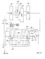
pixel engine 212 is coupled to receive the graphics data generated by thetriangle engine 208. Thepixel engine 212 contains circuitry for performing various graphics functions, such as, but not limited to, texture application or mapping, bilinear filtering, fog, blending, and color space conversion. Amemory controller 216 coupled to thepixel engine 212 and thegraphics processor 204 handles memory requests to and from alocal memory 220. Thelocal memory 220 stores graphics data, such as pixel values. Adisplay controller 224 is coupled to thememory controller 216 to receive processed values for pixels that are to be displayed. The output values from thedisplay controller 224 are subsequently provided to adisplay driver 232 that includes circuitry to provide digital signals, or convert digital signals to analog signals, to drive the display140 (FIG. 1). It will be appreciated that the circuitry included in thegraphics processing system 132 to practice embodiments of the present invention may be of conventional designs well understood by those of ordinary skill in the art. - Illustrated in FIG. 3 is portion of a memory system according to an embodiment of the present invention. An error correction code (ECC)[0018]
generator 302 andECC checking circuitry 304 are coupled to the input and output busses of an embedded memory306. The embedded memory306 is illustrated as having multiple banks of single-ported embedded memory306a-c.Although only three banks are shown in FIG. 3, it will be appreciated that the number of banks of embedded memory can be modified without departing from the scope of the present invention. The ECC generator and checkingcircuitry - Coupled to the[0019]
ECC generator 302 and theECC checking circuitry 304 is a memory310. The memory310 is divided intomemories memories selection circuits selection circuit 316 selectively couples data from either thememory 310aor thememory 310bto theECC generator 302 for calculation of an error correction code and storage in the embedded memory306. Theselection circuit 318, on the other hand, selects data from thememories memories combinatorial circuits selection circuits selection circuits memories ECC generator 302, or data being written to the embedded memory306. Thecombinatorial circuits selection circuits combinatorial circuits respective memories memories combinatorial circuits - A content addressable memory (CAM)[0020]350 is coupled to the memory310. The CAM350 is divided into
CAMs memories memories CAMs CAMs memories CAM - Control of the[0021]
selection circuits combinatorial circuits FIFO control circuit 356. Coordination of reading and writing data and memory addresses to the memory310 and the CAM350 are also under the control of theFIFO control circuit 356. As will be explained in more detail below, theFIFO control circuit 356 coordinates the operation of theselection circuits combinatorial circuits - As mentioned previously, the[0022]
selection circuits memories ECC generator 302 and the embedded memory306, or to provide data to a requesting entity in response to a read operation. Theselection circuits memories ECC check circuitry 304, or to receive write data. In an embodiment of the present invention, thememories - The operation of the memory system illustrated in FIG. 3 will now be described briefly, followed by a more detailed description of its operation.[0023]
- The[0024]
memories ECC generator 302 for the modified data can be performed in-line when writing the data back to the embedded memory306. This technique avoids the need to read the pre-processed data a second time from the embedded memory306 in order to calculate the correct ECC when performing a partial write operation. - In operation, when data is requested from the embedded memory[0025]306, the memory address of the requested data is stored in one of the
CAMs ECC check circuitry 304 to confirm the integrity of the data. Corrections to the requested data are made if necessary and if possible. The requested data is then written in its pre-processed form to the memory location ofmemory 310aormemory 310bthat is associated with the location in the CAM350 to which the memory address is written. Thus, when the address is provided again to the CAM350, the pre-processed data will be accessed in the associated memory location of memory310. As mentioned previously, coordination of the CAM350, theselection circuits combinatorial circuits FIFO control circuit 356 in order to write the requested data into the appropriate memory location of the memory310. The requested data is further output to theselection circuit 318 to be provided to the requesting entity. - In the case where the data has been requested for processing, for example, through a graphics processing pipeline, the post-processed data may need to be written back to the location in the embedded memory[0026]306 from which the data in its pre-processed from was retrieved. Further complicating the matter is that in the case of a partial write, it may be that only a portion of the entire data has been modified by the processing. Consequently, when writing the modified data back to the embedded memory306, a new error correction code will need to be calculated. In this situation, the entire length of data must be available and then combined with the partial write data before a new error correction code can be correctly calculated. In a conventional memory system, obtaining the full length of the pre-processed data requires a second read from the embedded memory, thus resulting in delays caused by the inherent memory access latency. Where data is being processed through a graphics processing pipeline such as one described in the aforementioned patent application, the additional delays in obtaining the pre-processed data, combining that data with the partial write data, and then calculating a new error correction code, will significantly reduce the processing throughput.
- In contrast to conventional memory systems, when performing a partial write in embodiments of the present invention, a second access to the embedded memory[0027]306 can be avoided because the pre-processed data is already present in the memory310 from when the data was originally read from the embedded memory306. Upon performing the partial write, the partial write data is provided to
selection circuits combinatorial circuit FIFO control circuit 356 directs theselection circuits combinatorial circuits - The modified data is then provided to the inputs of the[0028]
selection circuits FIFO control circuit 356 directs theselection circuit 316 to couple the output of thememories ECC generator 302. An error correction code is calculated, and the write operation is completed when the modified post-processed data is written to the memory location in the embedded memory306 that corresponds to the write address applied to the CAM350. - Although the previous example described the use of only one of the memories of the memory[0029]310 and one of the CAMs of the CAM350, having two
memories CAMs memories CAMs respective memory memory memories CAMs - For example, when a first read command is issued, the first read address is stored in[0030]
CAM 350aand the first pre-processed read data returned by the embedded memory306 is stored in the associated memory location in thememory 310a.The first pre-processed read data is also provided to the requesting entity through theselection circuit 318, which is under the control of theFIFO control circuit 356. Concurrently with the execution of the first read command, a first write command is issued. The first write address is applied to theCAM 350band the first post-processed write data is applied to the input of theselection circuits memory 310b,application of the address to theCAM 350bresults in the pre-processed data being output to thecombinatorial circuit 330. Under the control of theFIFO control circuit 356, theselection circuit 322 selects the write data to be applied to thecombinatorial circuit 330 in order to be combined with the pre-processed data. The resulting modified data is then output and provided through theselection circuit 316 toECC generator 302 to be written back to the embedded memory306. - At a time following the completion of the first read and write operations, a second read command is issued. A second read address for the second read command is directed to and stored in the[0031]
CAM 350b,and a second pre-processed read data from the embedded memory306 is stored in an associated memory location in thememory 310a.Theselection circuit 318 is then directed by theFIFO control circuit 356 to provide the second pre-processed read data to the requesting entity. Concurrently, a second write command is issued. It will be assumed that the pre-processed data that yielded the second post-processed write data is present in thememory 310a.Thus, application of the address to theCAM 350aresults in the pre-processed data being output to thecombinatorial circuit 320. Theselection circuit 322 is commanded to select the second post-processed write data to be applied to thecombinatorial circuit 320 in order to be combined with the pre-processed data just output by thememory 310a.To complete the second write command, the resulting combined data is then output and provided through theselection circuit 316 toECC generator 302 to be written back to the embedded memory306. - As illustrated by the previous example, interleaving the use of the memory and CAM sets,[0032]310aand350a, and310band350b,allows for read and write commands to be performed relatively concurrently. This feature is desirable where data is being processed through a graphics processing pipeline such as the one described in the aforementioned patent application. That is, the error correction capability of embodiments of the present invention can be combined with the read-modify-write technique provided by the processing pipeline structure and method to provide improved utilization of the read and write bandwidth of a graphics processing system while still including error correction capability.
- It will be appreciated that the capacity or length of the[0033]
memories memories - From the foregoing it will also be appreciated that, although specific embodiments of the invention have been described herein for purposes of illustration, various modifications may be made without deviating from the spirit and scope of the invention. Accordingly, the invention is not limited except as by the appended claims.[0034]
Claims (31)
Priority Applications (2)
| Application Number | Priority Date | Filing Date | Title |
|---|---|---|---|
| US09/974,364US6741253B2 (en) | 2001-10-09 | 2001-10-09 | Embedded memory system and method including data error correction |
| US10/813,184US6956577B2 (en) | 2001-10-09 | 2004-03-29 | Embedded memory system and method including data error correction |
Applications Claiming Priority (1)
| Application Number | Priority Date | Filing Date | Title |
|---|---|---|---|
| US09/974,364US6741253B2 (en) | 2001-10-09 | 2001-10-09 | Embedded memory system and method including data error correction |
Related Child Applications (1)
| Application Number | Title | Priority Date | Filing Date |
|---|---|---|---|
| US10/813,184ContinuationUS6956577B2 (en) | 2001-10-09 | 2004-03-29 | Embedded memory system and method including data error correction |
Publications (2)
| Publication Number | Publication Date |
|---|---|
| US20030067472A1true US20030067472A1 (en) | 2003-04-10 |
| US6741253B2 US6741253B2 (en) | 2004-05-25 |
Family
ID=29216555
Family Applications (2)
| Application Number | Title | Priority Date | Filing Date |
|---|---|---|---|
| US09/974,364Expired - LifetimeUS6741253B2 (en) | 2001-10-09 | 2001-10-09 | Embedded memory system and method including data error correction |
| US10/813,184Expired - LifetimeUS6956577B2 (en) | 2001-10-09 | 2004-03-29 | Embedded memory system and method including data error correction |
Family Applications After (1)
| Application Number | Title | Priority Date | Filing Date |
|---|---|---|---|
| US10/813,184Expired - LifetimeUS6956577B2 (en) | 2001-10-09 | 2004-03-29 | Embedded memory system and method including data error correction |
Country Status (1)
| Country | Link |
|---|---|
| US (2) | US6741253B2 (en) |
Cited By (11)
| Publication number | Priority date | Publication date | Assignee | Title |
|---|---|---|---|---|
| US20030131024A1 (en)* | 1996-07-30 | 2003-07-10 | Carlos De La Huerga | Method for verifying record code prior to an action based on the code |
| US7013298B1 (en) | 1996-07-30 | 2006-03-14 | Hyperphrase Technologies, Llc | Method and system for automated data storage and retrieval |
| US20060101231A1 (en)* | 2004-09-28 | 2006-05-11 | Renesas Technology Corp. | Semiconductor signal processing device |
| US20070033467A1 (en)* | 2005-07-08 | 2007-02-08 | Stmicroelectronics Sa | Method and device for protecting a memory against attacks by error injection |
| US20070206434A1 (en)* | 2006-03-01 | 2007-09-06 | Radke William H | Memory with multi-page read |
| US20080037320A1 (en)* | 2006-08-14 | 2008-02-14 | Micron Technology, Inc. | Flash memory with multi-bit read |
| WO2010107176A3 (en)* | 2009-03-19 | 2010-11-11 | (주)인디링스 | Apparatus and method for managing a dram buffer |
| WO2011025474A1 (en)* | 2009-08-25 | 2011-03-03 | Hewlett-Packard Development Company, L.P. | Error correcting |
| US8429391B2 (en) | 2010-04-16 | 2013-04-23 | Micron Technology, Inc. | Boot partitions in memory devices and systems |
| US8451664B2 (en) | 2010-05-12 | 2013-05-28 | Micron Technology, Inc. | Determining and using soft data in memory devices and systems |
| CN112766875A (en)* | 2020-12-29 | 2021-05-07 | 金蝶软件(中国)有限公司 | Receipt data processing method and device, computer equipment and storage medium |
Families Citing this family (33)
| Publication number | Priority date | Publication date | Assignee | Title |
|---|---|---|---|---|
| US6784889B1 (en) | 2000-12-13 | 2004-08-31 | Micron Technology, Inc. | Memory system and method for improved utilization of read and write bandwidth of a graphics processing system |
| US6700827B2 (en) | 2001-02-08 | 2004-03-02 | Integrated Device Technology, Inc. | Cam circuit with error correction |
| US7301961B1 (en) | 2001-12-27 | 2007-11-27 | Cypress Semiconductor Corportion | Method and apparatus for configuring signal lines according to idle codes |
| US7200793B1 (en)* | 2002-03-22 | 2007-04-03 | Altera Corporation | Error checking and correcting for content addressable memories (CAMs) |
| US7399043B2 (en)* | 2002-12-02 | 2008-07-15 | Silverbrook Research Pty Ltd | Compensation for uneven printhead module lengths in a multi-module printhead |
| US6870749B1 (en) | 2003-07-15 | 2005-03-22 | Integrated Device Technology, Inc. | Content addressable memory (CAM) devices with dual-function check bit cells that support column redundancy and check bit cells with reduced susceptibility to soft errors |
| US6987684B1 (en) | 2003-07-15 | 2006-01-17 | Integrated Device Technology, Inc. | Content addressable memory (CAM) devices having multi-block error detection logic and entry selective error correction logic therein |
| US7193876B1 (en) | 2003-07-15 | 2007-03-20 | Kee Park | Content addressable memory (CAM) arrays having memory cells therein with different susceptibilities to soft errors |
| US7304875B1 (en) | 2003-12-17 | 2007-12-04 | Integrated Device Technology. Inc. | Content addressable memory (CAM) devices that support background BIST and BISR operations and methods of operating same |
| US7304873B1 (en) | 2005-01-25 | 2007-12-04 | Netlogic Microsystems, Inc. | Method for on-the-fly error correction in a content addressable memory (CAM) and device therefor |
| US7444579B2 (en) | 2005-04-28 | 2008-10-28 | Micron Technology, Inc. | Non-systematic coded error correction |
| US7810017B2 (en)* | 2006-03-20 | 2010-10-05 | Micron Technology, Inc. | Variable sector-count ECC |
| US7953907B1 (en) | 2006-08-22 | 2011-05-31 | Marvell International Ltd. | Concurrent input/output control and integrated error management in FIFO |
| US7739576B2 (en)* | 2006-08-31 | 2010-06-15 | Micron Technology, Inc. | Variable strength ECC |
| US7747903B2 (en)* | 2007-07-09 | 2010-06-29 | Micron Technology, Inc. | Error correction for memory |
| US20090083495A1 (en)* | 2007-09-26 | 2009-03-26 | Khellah Muhammad M | Memory circuit with ecc based writeback |
| JP2010152542A (en)* | 2008-12-24 | 2010-07-08 | Toshiba Corp | Memory system |
| US7821843B2 (en)* | 2009-03-06 | 2010-10-26 | Texas Instruments Incorporated | Partial write-back in read and write-back of a memory |
| JP2010262496A (en)* | 2009-05-08 | 2010-11-18 | Fujitsu Ltd | Memory control method and memory control device |
| JP4793741B2 (en)* | 2009-07-24 | 2011-10-12 | エヌイーシーコンピュータテクノ株式会社 | Error correction circuit and error correction method |
| US8077515B2 (en) | 2009-08-25 | 2011-12-13 | Micron Technology, Inc. | Methods, devices, and systems for dealing with threshold voltage change in memory devices |
| US8271697B2 (en) | 2009-09-29 | 2012-09-18 | Micron Technology, Inc. | State change in systems having devices coupled in a chained configuration |
| US8392807B2 (en)* | 2010-07-23 | 2013-03-05 | Sandisk Technologies Inc. | System and method of distributive ECC processing |
| US8553441B1 (en) | 2010-08-31 | 2013-10-08 | Netlogic Microsystems, Inc. | Ternary content addressable memory cell having two transistor pull-down stack |
| US8625320B1 (en) | 2010-08-31 | 2014-01-07 | Netlogic Microsystems, Inc. | Quaternary content addressable memory cell having one transistor pull-down stack |
| US8582338B1 (en) | 2010-08-31 | 2013-11-12 | Netlogic Microsystems, Inc. | Ternary content addressable memory cell having single transistor pull-down stack |
| US8462532B1 (en) | 2010-08-31 | 2013-06-11 | Netlogic Microsystems, Inc. | Fast quaternary content addressable memory cell |
| US20120110411A1 (en)* | 2010-10-29 | 2012-05-03 | Brocade Communications Systems, Inc. | Content Addressable Memory (CAM) Parity And Error Correction Code (ECC) Protection |
| US8837188B1 (en) | 2011-06-23 | 2014-09-16 | Netlogic Microsystems, Inc. | Content addressable memory row having virtual ground and charge sharing |
| US8773880B2 (en) | 2011-06-23 | 2014-07-08 | Netlogic Microsystems, Inc. | Content addressable memory array having virtual ground nodes |
| US8984195B2 (en)* | 2011-12-02 | 2015-03-17 | Atmel Corporation | Microcontroller including alternative links between peripherals for resource sharing |
| US9069705B2 (en)* | 2013-02-26 | 2015-06-30 | Oracle International Corporation | CAM bit error recovery |
| WO2015048037A1 (en) | 2013-09-24 | 2015-04-02 | Rambus Inc. | Memory component having internal read-modify-write operation |
Citations (8)
| Publication number | Priority date | Publication date | Assignee | Title |
|---|---|---|---|---|
| US5809228A (en)* | 1995-12-27 | 1998-09-15 | Intel Corporaiton | Method and apparatus for combining multiple writes to a memory resource utilizing a write buffer |
| US5860112A (en)* | 1995-12-27 | 1999-01-12 | Intel Corporation | Method and apparatus for blending bus writes and cache write-backs to memory |
| US5987628A (en)* | 1997-11-26 | 1999-11-16 | Intel Corporation | Method and apparatus for automatically correcting errors detected in a memory subsystem |
| US6115837A (en)* | 1998-07-29 | 2000-09-05 | Neomagic Corp. | Dual-column syndrome generation for DVD error correction using an embedded DRAM |
| US6151658A (en)* | 1998-01-16 | 2000-11-21 | Advanced Micro Devices, Inc. | Write-buffer FIFO architecture with random access snooping capability |
| US6272651B1 (en)* | 1998-08-17 | 2001-08-07 | Compaq Computer Corp. | System and method for improving processor read latency in a system employing error checking and correction |
| US6366984B1 (en)* | 1999-05-11 | 2002-04-02 | Intel Corporation | Write combining buffer that supports snoop request |
| US6401168B1 (en)* | 1999-01-04 | 2002-06-04 | Texas Instruments Incorporated | FIFO disk data path manager and method |
Family Cites Families (13)
| Publication number | Priority date | Publication date | Assignee | Title |
|---|---|---|---|---|
| CA2070934C (en) | 1992-06-10 | 1998-05-05 | Benny Chi Wah Lau | Graphics display system |
| US5831673A (en) | 1994-01-25 | 1998-11-03 | Przyborski; Glenn B. | Method and apparatus for storing and displaying images provided by a video signal that emulates the look of motion picture film |
| US6104417A (en)* | 1996-09-13 | 2000-08-15 | Silicon Graphics, Inc. | Unified memory computer architecture with dynamic graphics memory allocation |
| US5924117A (en) | 1996-12-16 | 1999-07-13 | International Business Machines Corporation | Multi-ported and interleaved cache memory supporting multiple simultaneous accesses thereto |
| US6112265A (en) | 1997-04-07 | 2000-08-29 | Intel Corportion | System for issuing a command to a memory having a reorder module for priority commands and an arbiter tracking address of recently issued command |
| US6002412A (en) | 1997-05-30 | 1999-12-14 | Hewlett-Packard Co. | Increased performance of graphics memory using page sorting fifos |
| US6150679A (en) | 1998-03-13 | 2000-11-21 | Hewlett Packard Company | FIFO architecture with built-in intelligence for use in a graphics memory system for reducing paging overhead |
| US6167551A (en)* | 1998-07-29 | 2000-12-26 | Neomagic Corp. | DVD controller with embedded DRAM for ECC-block buffering |
| US6279135B1 (en)* | 1998-07-29 | 2001-08-21 | Lsi Logic Corporation | On-the-fly row-syndrome generation for DVD controller ECC |
| US6523110B1 (en) | 1999-07-23 | 2003-02-18 | International Business Machines Corporation | Decoupled fetch-execute engine with static branch prediction support |
| US6470433B1 (en) | 2000-04-29 | 2002-10-22 | Hewlett-Packard Company | Modified aggressive precharge DRAM controller |
| US6587112B1 (en) | 2000-07-10 | 2003-07-01 | Hewlett-Packard Development Company, L.P. | Window copy-swap using multi-buffer hardware support |
| US6784889B1 (en)* | 2000-12-13 | 2004-08-31 | Micron Technology, Inc. | Memory system and method for improved utilization of read and write bandwidth of a graphics processing system |
- 2001
- 2001-10-09USUS09/974,364patent/US6741253B2/ennot_activeExpired - Lifetime
- 2004
- 2004-03-29USUS10/813,184patent/US6956577B2/ennot_activeExpired - Lifetime
Patent Citations (8)
| Publication number | Priority date | Publication date | Assignee | Title |
|---|---|---|---|---|
| US5809228A (en)* | 1995-12-27 | 1998-09-15 | Intel Corporaiton | Method and apparatus for combining multiple writes to a memory resource utilizing a write buffer |
| US5860112A (en)* | 1995-12-27 | 1999-01-12 | Intel Corporation | Method and apparatus for blending bus writes and cache write-backs to memory |
| US5987628A (en)* | 1997-11-26 | 1999-11-16 | Intel Corporation | Method and apparatus for automatically correcting errors detected in a memory subsystem |
| US6151658A (en)* | 1998-01-16 | 2000-11-21 | Advanced Micro Devices, Inc. | Write-buffer FIFO architecture with random access snooping capability |
| US6115837A (en)* | 1998-07-29 | 2000-09-05 | Neomagic Corp. | Dual-column syndrome generation for DVD error correction using an embedded DRAM |
| US6272651B1 (en)* | 1998-08-17 | 2001-08-07 | Compaq Computer Corp. | System and method for improving processor read latency in a system employing error checking and correction |
| US6401168B1 (en)* | 1999-01-04 | 2002-06-04 | Texas Instruments Incorporated | FIFO disk data path manager and method |
| US6366984B1 (en)* | 1999-05-11 | 2002-04-02 | Intel Corporation | Write combining buffer that supports snoop request |
Cited By (29)
| Publication number | Priority date | Publication date | Assignee | Title |
|---|---|---|---|---|
| US6820093B2 (en)* | 1996-07-30 | 2004-11-16 | Hyperphrase Technologies, Llc | Method for verifying record code prior to an action based on the code |
| US7013298B1 (en) | 1996-07-30 | 2006-03-14 | Hyperphrase Technologies, Llc | Method and system for automated data storage and retrieval |
| US20030131024A1 (en)* | 1996-07-30 | 2003-07-10 | Carlos De La Huerga | Method for verifying record code prior to an action based on the code |
| US20060101231A1 (en)* | 2004-09-28 | 2006-05-11 | Renesas Technology Corp. | Semiconductor signal processing device |
| US7788506B2 (en)* | 2005-07-08 | 2010-08-31 | Stmicroelectronics Sa | Method and device for protecting a memory against attacks by error injection |
| US20070033467A1 (en)* | 2005-07-08 | 2007-02-08 | Stmicroelectronics Sa | Method and device for protecting a memory against attacks by error injection |
| US7453723B2 (en) | 2006-03-01 | 2008-11-18 | Micron Technology, Inc. | Memory with weighted multi-page read |
| US20090067249A1 (en)* | 2006-03-01 | 2009-03-12 | William Henry Radke | Memory with multi-page read |
| US20070206434A1 (en)* | 2006-03-01 | 2007-09-06 | Radke William H | Memory with multi-page read |
| US7990763B2 (en) | 2006-03-01 | 2011-08-02 | Micron Technology, Inc. | Memory with weighted multi-page read |
| US8670272B2 (en) | 2006-03-01 | 2014-03-11 | Micron Technology, Inc. | Memory with weighted multi-page read |
| US8331143B2 (en) | 2006-03-01 | 2012-12-11 | Micron Technology, Inc. | Memory with multi-page read |
| US7369434B2 (en) | 2006-08-14 | 2008-05-06 | Micron Technology, Inc. | Flash memory with multi-bit read |
| US7738292B2 (en) | 2006-08-14 | 2010-06-15 | Micron Technology, Inc. | Flash memory with multi-bit read |
| US20080037320A1 (en)* | 2006-08-14 | 2008-02-14 | Micron Technology, Inc. | Flash memory with multi-bit read |
| US20100238726A1 (en)* | 2006-08-14 | 2010-09-23 | William Henry Radke | Flash memory with multi-bit read |
| US8189387B2 (en) | 2006-08-14 | 2012-05-29 | Micron Technology, Inc. | Flash memory with multi-bit read |
| JP2012521033A (en)* | 2009-03-19 | 2012-09-10 | インディリンクス カンパニー リミテッド | DRAM buffer management apparatus and method |
| WO2010107176A3 (en)* | 2009-03-19 | 2010-11-11 | (주)인디링스 | Apparatus and method for managing a dram buffer |
| WO2011025474A1 (en)* | 2009-08-25 | 2011-03-03 | Hewlett-Packard Development Company, L.P. | Error correcting |
| US20120151300A1 (en)* | 2009-08-25 | 2012-06-14 | Tillema John E | Error Correcting |
| CN102483710A (en)* | 2009-08-25 | 2012-05-30 | 惠普发展公司,有限责任合伙企业 | Error correcting |
| US8429391B2 (en) | 2010-04-16 | 2013-04-23 | Micron Technology, Inc. | Boot partitions in memory devices and systems |
| US8762703B2 (en) | 2010-04-16 | 2014-06-24 | Micron Technology, Inc. | Boot partitions in memory devices and systems |
| US9342371B2 (en) | 2010-04-16 | 2016-05-17 | Micron Technology, Inc. | Boot partitions in memory devices and systems |
| US8451664B2 (en) | 2010-05-12 | 2013-05-28 | Micron Technology, Inc. | Determining and using soft data in memory devices and systems |
| US9177659B2 (en) | 2010-05-12 | 2015-11-03 | Micron Technology, Inc. | Determining and using soft data in memory devices and systems |
| US9293214B2 (en) | 2010-05-12 | 2016-03-22 | Micron Technology, Inc. | Determining and using soft data in memory devices and systems |
| CN112766875A (en)* | 2020-12-29 | 2021-05-07 | 金蝶软件(中国)有限公司 | Receipt data processing method and device, computer equipment and storage medium |
Also Published As
| Publication number | Publication date |
|---|---|
| US20040183808A1 (en) | 2004-09-23 |
| US6956577B2 (en) | 2005-10-18 |
| US6741253B2 (en) | 2004-05-25 |
Similar Documents
| Publication | Publication Date | Title |
|---|---|---|
| US6741253B2 (en) | Embedded memory system and method including data error correction | |
| US8194086B2 (en) | Memory system and method for improved utilization of read and write bandwidth of a graphics processing system | |
| US6943800B2 (en) | Method and apparatus for updating state data | |
| US6195106B1 (en) | Graphics system with multiported pixel buffers for accelerated pixel processing | |
| JP3779748B2 (en) | Frame buffer memory, computer system, pixel access method, and block fill operation method | |
| US8704840B2 (en) | Memory system having multiple address allocation formats and method for use thereof | |
| US6999087B2 (en) | Dynamically adjusting sample density in a graphics system | |
| US8245109B2 (en) | Error checking and correction (ECC) system and method | |
| US20050030313A1 (en) | Apparatus and method for distributed memory control in a graphics processing system | |
| JPH0348370A (en) | Memory access control circuit | |
| US20080036764A1 (en) | Method and apparatus for processing computer graphics data | |
| US7542046B1 (en) | Programmable clipping engine for clipping graphics primitives | |
| JPH0355832B2 (en) | ||
| US20030095124A1 (en) | Back-end image transformation | |
| US20060007247A1 (en) | Graphics resampling system and method for use thereof | |
| US6667930B1 (en) | System and method for optimizing performance in a four-bank SDRAM | |
| US8139073B1 (en) | Early compression tag lookup for memory accesses | |
| US6734865B1 (en) | Method and system for mapping various length data regions | |
| US8156404B1 (en) | L2 ECC implementation | |
| US6963343B1 (en) | Apparatus and method for dynamically disabling faulty embedded memory in a graphic processing system | |
| US8099650B1 (en) | L2 ECC implementation | |
| US6362824B1 (en) | System-wide texture offset addressing with page residence indicators for improved performance | |
| JPH0765198A (en) | Image memory device | |
| JPH02234251A (en) | Control system for extended storage | |
| JP2002108692A (en) | Semiconductor memory device and information processing method |
Legal Events
| Date | Code | Title | Description |
|---|---|---|---|
| AS | Assignment | Owner name:MICRON TECHNOLOGY, INC., IDAHO Free format text:ASSIGNMENT OF ASSIGNORS INTEREST;ASSIGNORS:RADKE, WILLIAM;SARWARI, ATIF;REEL/FRAME:012249/0692;SIGNING DATES FROM 20010717 TO 20010912 | |
| FEPP | Fee payment procedure | Free format text:PAYOR NUMBER ASSIGNED (ORIGINAL EVENT CODE: ASPN); ENTITY STATUS OF PATENT OWNER: LARGE ENTITY | |
| STCF | Information on status: patent grant | Free format text:PATENTED CASE | |
| CC | Certificate of correction | ||
| CC | Certificate of correction | ||
| FPAY | Fee payment | Year of fee payment:4 | |
| FPAY | Fee payment | Year of fee payment:8 | |
| FPAY | Fee payment | Year of fee payment:12 | |
| AS | Assignment | Owner name:U.S. BANK NATIONAL ASSOCIATION, AS COLLATERAL AGENT, CALIFORNIA Free format text:SECURITY INTEREST;ASSIGNOR:MICRON TECHNOLOGY, INC.;REEL/FRAME:038669/0001 Effective date:20160426 Owner name:U.S. BANK NATIONAL ASSOCIATION, AS COLLATERAL AGEN Free format text:SECURITY INTEREST;ASSIGNOR:MICRON TECHNOLOGY, INC.;REEL/FRAME:038669/0001 Effective date:20160426 | |
| AS | Assignment | Owner name:MORGAN STANLEY SENIOR FUNDING, INC., AS COLLATERAL AGENT, MARYLAND Free format text:PATENT SECURITY AGREEMENT;ASSIGNOR:MICRON TECHNOLOGY, INC.;REEL/FRAME:038954/0001 Effective date:20160426 Owner name:MORGAN STANLEY SENIOR FUNDING, INC., AS COLLATERAL Free format text:PATENT SECURITY AGREEMENT;ASSIGNOR:MICRON TECHNOLOGY, INC.;REEL/FRAME:038954/0001 Effective date:20160426 | |
| AS | Assignment | Owner name:U.S. BANK NATIONAL ASSOCIATION, AS COLLATERAL AGENT, CALIFORNIA Free format text:CORRECTIVE ASSIGNMENT TO CORRECT THE REPLACE ERRONEOUSLY FILED PATENT #7358718 WITH THE CORRECT PATENT #7358178 PREVIOUSLY RECORDED ON REEL 038669 FRAME 0001. ASSIGNOR(S) HEREBY CONFIRMS THE SECURITY INTEREST;ASSIGNOR:MICRON TECHNOLOGY, INC.;REEL/FRAME:043079/0001 Effective date:20160426 Owner name:U.S. BANK NATIONAL ASSOCIATION, AS COLLATERAL AGEN Free format text:CORRECTIVE ASSIGNMENT TO CORRECT THE REPLACE ERRONEOUSLY FILED PATENT #7358718 WITH THE CORRECT PATENT #7358178 PREVIOUSLY RECORDED ON REEL 038669 FRAME 0001. ASSIGNOR(S) HEREBY CONFIRMS THE SECURITY INTEREST;ASSIGNOR:MICRON TECHNOLOGY, INC.;REEL/FRAME:043079/0001 Effective date:20160426 | |
| AS | Assignment | Owner name:JPMORGAN CHASE BANK, N.A., AS COLLATERAL AGENT, ILLINOIS Free format text:SECURITY INTEREST;ASSIGNORS:MICRON TECHNOLOGY, INC.;MICRON SEMICONDUCTOR PRODUCTS, INC.;REEL/FRAME:047540/0001 Effective date:20180703 Owner name:JPMORGAN CHASE BANK, N.A., AS COLLATERAL AGENT, IL Free format text:SECURITY INTEREST;ASSIGNORS:MICRON TECHNOLOGY, INC.;MICRON SEMICONDUCTOR PRODUCTS, INC.;REEL/FRAME:047540/0001 Effective date:20180703 | |
| AS | Assignment | Owner name:MICRON TECHNOLOGY, INC., IDAHO Free format text:RELEASE BY SECURED PARTY;ASSIGNOR:U.S. BANK NATIONAL ASSOCIATION, AS COLLATERAL AGENT;REEL/FRAME:047243/0001 Effective date:20180629 | |
| AS | Assignment | Owner name:MICRON TECHNOLOGY, INC., IDAHO Free format text:RELEASE BY SECURED PARTY;ASSIGNOR:MORGAN STANLEY SENIOR FUNDING, INC., AS COLLATERAL AGENT;REEL/FRAME:050937/0001 Effective date:20190731 | |
| AS | Assignment | Owner name:MICRON TECHNOLOGY, INC., IDAHO Free format text:RELEASE BY SECURED PARTY;ASSIGNOR:JPMORGAN CHASE BANK, N.A., AS COLLATERAL AGENT;REEL/FRAME:051028/0001 Effective date:20190731 Owner name:MICRON SEMICONDUCTOR PRODUCTS, INC., IDAHO Free format text:RELEASE BY SECURED PARTY;ASSIGNOR:JPMORGAN CHASE BANK, N.A., AS COLLATERAL AGENT;REEL/FRAME:051028/0001 Effective date:20190731 |