US20030067057A1 - Lead frame and flip chip semiconductor package with the same - Google Patents
Lead frame and flip chip semiconductor package with the sameDownload PDFInfo
- Publication number
- US20030067057A1 US20030067057A1US09/973,358US97335801AUS2003067057A1US 20030067057 A1US20030067057 A1US 20030067057A1US 97335801 AUS97335801 AUS 97335801AUS 2003067057 A1US2003067057 A1US 2003067057A1
- Authority
- US
- United States
- Prior art keywords
- lead frame
- die pad
- solder bumps
- leads
- semiconductor package
- Prior art date
- Legal status (The legal status is an assumption and is not a legal conclusion. Google has not performed a legal analysis and makes no representation as to the accuracy of the status listed.)
- Granted
Links
- 239000004065semiconductorSubstances0.000titleclaimsabstractdescription74
- 229910000679solderInorganic materials0.000claimsabstractdescription64
- 238000000034methodMethods0.000claimsabstractdescription23
- 239000000853adhesiveSubstances0.000claimsdescription10
- 230000001070adhesive effectEffects0.000claimsdescription10
- 230000008018meltingEffects0.000claimsdescription6
- 238000002844meltingMethods0.000claimsdescription6
- 239000008393encapsulating agentSubstances0.000claimsdescription5
- 238000005530etchingMethods0.000claimsdescription4
- 239000007769metal materialSubstances0.000claimsdescription4
- 238000004080punchingMethods0.000claimsdescription4
- 239000002184metalSubstances0.000claimsdescription3
- 229910052751metalInorganic materials0.000claimsdescription3
- 230000008569processEffects0.000abstractdescription18
- 238000004519manufacturing processMethods0.000description5
- ATJFFYVFTNAWJD-UHFFFAOYSA-NTinChemical compound[Sn]ATJFFYVFTNAWJD-UHFFFAOYSA-N0.000description4
- 238000005516engineering processMethods0.000description4
- PCHJSUWPFVWCPO-UHFFFAOYSA-NgoldChemical compound[Au]PCHJSUWPFVWCPO-UHFFFAOYSA-N0.000description4
- 239000010931goldSubstances0.000description4
- 229910052737goldInorganic materials0.000description4
- RYGMFSIKBFXOCR-UHFFFAOYSA-NCopperChemical compound[Cu]RYGMFSIKBFXOCR-UHFFFAOYSA-N0.000description3
- 229910045601alloyInorganic materials0.000description3
- 239000000956alloySubstances0.000description3
- 230000015572biosynthetic processEffects0.000description3
- 229910052802copperInorganic materials0.000description3
- 239000010949copperSubstances0.000description3
- XEEYBQQBJWHFJM-UHFFFAOYSA-NIronChemical compound[Fe]XEEYBQQBJWHFJM-UHFFFAOYSA-N0.000description2
- PXHVJJICTQNCMI-UHFFFAOYSA-NNickelChemical compound[Ni]PXHVJJICTQNCMI-UHFFFAOYSA-N0.000description2
- 238000010586diagramMethods0.000description2
- 230000005484gravityEffects0.000description2
- 230000017525heat dissipationEffects0.000description2
- 229910000765intermetallicInorganic materials0.000description2
- 238000012986modificationMethods0.000description2
- 230000004048modificationEffects0.000description2
- 229910000640Fe alloyInorganic materials0.000description1
- 241000272168LaridaeSpecies0.000description1
- 229910000990Ni alloyInorganic materials0.000description1
- 229910000978Pb alloyInorganic materials0.000description1
- 229910001128Sn alloyInorganic materials0.000description1
- 230000009286beneficial effectEffects0.000description1
- 238000005336crackingMethods0.000description1
- 238000005520cutting processMethods0.000description1
- 238000009826distributionMethods0.000description1
- 230000005496eutecticsEffects0.000description1
- 238000010438heat treatmentMethods0.000description1
- 238000002513implantationMethods0.000description1
- 230000010354integrationEffects0.000description1
- 238000001459lithographyMethods0.000description1
- 239000000203mixtureSubstances0.000description1
- 229910052759nickelInorganic materials0.000description1
- 230000009467reductionEffects0.000description1
- 238000007650screen-printingMethods0.000description1
- 229910052709silverInorganic materials0.000description1
- 239000004332silverSubstances0.000description1
- 238000009736wettingMethods0.000description1
Images


Classifications
- H—ELECTRICITY
- H01—ELECTRIC ELEMENTS
- H01L—SEMICONDUCTOR DEVICES NOT COVERED BY CLASS H10
- H01L23/00—Details of semiconductor or other solid state devices
- H01L23/48—Arrangements for conducting electric current to or from the solid state body in operation, e.g. leads, terminal arrangements ; Selection of materials therefor
- H01L23/488—Arrangements for conducting electric current to or from the solid state body in operation, e.g. leads, terminal arrangements ; Selection of materials therefor consisting of soldered or bonded constructions
- H01L23/495—Lead-frames or other flat leads
- H01L23/49541—Geometry of the lead-frame
- H01L23/49548—Cross section geometry
- H01L23/49551—Cross section geometry characterised by bent parts
- H01L23/49555—Cross section geometry characterised by bent parts the bent parts being the outer leads
- H—ELECTRICITY
- H01—ELECTRIC ELEMENTS
- H01L—SEMICONDUCTOR DEVICES NOT COVERED BY CLASS H10
- H01L2224/00—Indexing scheme for arrangements for connecting or disconnecting semiconductor or solid-state bodies and methods related thereto as covered by H01L24/00
- H01L2224/01—Means for bonding being attached to, or being formed on, the surface to be connected, e.g. chip-to-package, die-attach, "first-level" interconnects; Manufacturing methods related thereto
- H01L2224/02—Bonding areas; Manufacturing methods related thereto
- H01L2224/04—Structure, shape, material or disposition of the bonding areas prior to the connecting process
- H01L2224/05—Structure, shape, material or disposition of the bonding areas prior to the connecting process of an individual bonding area
- H01L2224/0554—External layer
- H01L2224/0556—Disposition
- H01L2224/05568—Disposition the whole external layer protruding from the surface
- H—ELECTRICITY
- H01—ELECTRIC ELEMENTS
- H01L—SEMICONDUCTOR DEVICES NOT COVERED BY CLASS H10
- H01L2224/00—Indexing scheme for arrangements for connecting or disconnecting semiconductor or solid-state bodies and methods related thereto as covered by H01L24/00
- H01L2224/01—Means for bonding being attached to, or being formed on, the surface to be connected, e.g. chip-to-package, die-attach, "first-level" interconnects; Manufacturing methods related thereto
- H01L2224/02—Bonding areas; Manufacturing methods related thereto
- H01L2224/04—Structure, shape, material or disposition of the bonding areas prior to the connecting process
- H01L2224/05—Structure, shape, material or disposition of the bonding areas prior to the connecting process of an individual bonding area
- H01L2224/0554—External layer
- H01L2224/05573—Single external layer
- H—ELECTRICITY
- H01—ELECTRIC ELEMENTS
- H01L—SEMICONDUCTOR DEVICES NOT COVERED BY CLASS H10
- H01L2224/00—Indexing scheme for arrangements for connecting or disconnecting semiconductor or solid-state bodies and methods related thereto as covered by H01L24/00
- H01L2224/01—Means for bonding being attached to, or being formed on, the surface to be connected, e.g. chip-to-package, die-attach, "first-level" interconnects; Manufacturing methods related thereto
- H01L2224/10—Bump connectors; Manufacturing methods related thereto
- H01L2224/15—Structure, shape, material or disposition of the bump connectors after the connecting process
- H01L2224/16—Structure, shape, material or disposition of the bump connectors after the connecting process of an individual bump connector
- H01L2224/161—Disposition
- H01L2224/16151—Disposition the bump connector connecting between a semiconductor or solid-state body and an item not being a semiconductor or solid-state body, e.g. chip-to-substrate, chip-to-passive
- H01L2224/16221—Disposition the bump connector connecting between a semiconductor or solid-state body and an item not being a semiconductor or solid-state body, e.g. chip-to-substrate, chip-to-passive the body and the item being stacked
- H01L2224/16245—Disposition the bump connector connecting between a semiconductor or solid-state body and an item not being a semiconductor or solid-state body, e.g. chip-to-substrate, chip-to-passive the body and the item being stacked the item being metallic
- H—ELECTRICITY
- H01—ELECTRIC ELEMENTS
- H01L—SEMICONDUCTOR DEVICES NOT COVERED BY CLASS H10
- H01L2224/00—Indexing scheme for arrangements for connecting or disconnecting semiconductor or solid-state bodies and methods related thereto as covered by H01L24/00
- H01L2224/01—Means for bonding being attached to, or being formed on, the surface to be connected, e.g. chip-to-package, die-attach, "first-level" interconnects; Manufacturing methods related thereto
- H01L2224/42—Wire connectors; Manufacturing methods related thereto
- H01L2224/44—Structure, shape, material or disposition of the wire connectors prior to the connecting process
- H01L2224/45—Structure, shape, material or disposition of the wire connectors prior to the connecting process of an individual wire connector
- H01L2224/45001—Core members of the connector
- H01L2224/45099—Material
- H01L2224/451—Material with a principal constituent of the material being a metal or a metalloid, e.g. boron (B), silicon (Si), germanium (Ge), arsenic (As), antimony (Sb), tellurium (Te) and polonium (Po), and alloys thereof
- H01L2224/45138—Material with a principal constituent of the material being a metal or a metalloid, e.g. boron (B), silicon (Si), germanium (Ge), arsenic (As), antimony (Sb), tellurium (Te) and polonium (Po), and alloys thereof the principal constituent melting at a temperature of greater than or equal to 950°C and less than 1550°C
- H01L2224/45144—Gold (Au) as principal constituent
- H—ELECTRICITY
- H01—ELECTRIC ELEMENTS
- H01L—SEMICONDUCTOR DEVICES NOT COVERED BY CLASS H10
- H01L2224/00—Indexing scheme for arrangements for connecting or disconnecting semiconductor or solid-state bodies and methods related thereto as covered by H01L24/00
- H01L2224/73—Means for bonding being of different types provided for in two or more of groups H01L2224/10, H01L2224/18, H01L2224/26, H01L2224/34, H01L2224/42, H01L2224/50, H01L2224/63, H01L2224/71
- H01L2224/732—Location after the connecting process
- H01L2224/73201—Location after the connecting process on the same surface
- H01L2224/73203—Bump and layer connectors
- H01L2224/73204—Bump and layer connectors the bump connector being embedded into the layer connector
- H—ELECTRICITY
- H01—ELECTRIC ELEMENTS
- H01L—SEMICONDUCTOR DEVICES NOT COVERED BY CLASS H10
- H01L2924/00—Indexing scheme for arrangements or methods for connecting or disconnecting semiconductor or solid-state bodies as covered by H01L24/00
- H01L2924/0001—Technical content checked by a classifier
- H01L2924/00014—Technical content checked by a classifier the subject-matter covered by the group, the symbol of which is combined with the symbol of this group, being disclosed without further technical details
- H—ELECTRICITY
- H01—ELECTRIC ELEMENTS
- H01L—SEMICONDUCTOR DEVICES NOT COVERED BY CLASS H10
- H01L2924/00—Indexing scheme for arrangements or methods for connecting or disconnecting semiconductor or solid-state bodies as covered by H01L24/00
- H01L2924/01—Chemical elements
- H01L2924/01079—Gold [Au]
- H—ELECTRICITY
- H01—ELECTRIC ELEMENTS
- H01L—SEMICONDUCTOR DEVICES NOT COVERED BY CLASS H10
- H01L2924/00—Indexing scheme for arrangements or methods for connecting or disconnecting semiconductor or solid-state bodies as covered by H01L24/00
- H01L2924/013—Alloys
- H01L2924/0132—Binary Alloys
- H01L2924/01322—Eutectic Alloys, i.e. obtained by a liquid transforming into two solid phases
- H—ELECTRICITY
- H01—ELECTRIC ELEMENTS
- H01L—SEMICONDUCTOR DEVICES NOT COVERED BY CLASS H10
- H01L2924/00—Indexing scheme for arrangements or methods for connecting or disconnecting semiconductor or solid-state bodies as covered by H01L24/00
- H01L2924/013—Alloys
- H01L2924/0132—Binary Alloys
- H01L2924/01327—Intermediate phases, i.e. intermetallics compounds
Definitions
- the present inventionrelates to semiconductor packages, and more particularly to a semiconductor package, in which a semiconductor chip is mounted in a flip chip manner on a lead frame.
- a semiconductor devicetends to be made in low cost, high performance and high integration, and is also preferably dimensioned with reduction in size and overall thickness thereof, in correspondence to a trend of low-profile electronic products.
- a QFN (quad-flat non-leaded) semiconductor packageis a mainstream conventional product, due to advantages in that the QFN semiconductor package is only slightly larger in dimension than a semiconductor chip mounted therein, and is cost-effectively made in a lead frame based batch manner.
- a semiconductor device 4comprises a lead frame (not shown), which is made of a metallic material such as copper, and mainly consists of a plurality of leads 42 variable in length; a plurality of semiconductor chips 43 each having an active surface 430 disposed with a plurality of bonding pads thereon, and a non-active surface 431 ; a plurality of solder bumps 44 implanted on the bonding pads 432 , allowing the leads 42 to be reflowed on each of front and back surfaces thereof with one of the chips 43 in a manner that the active surface 430 of the chip 43 faces the leads 42 ; and an encapsulant 45 formed on the leads 42 for encapsulating the semiconductor chips 43 .
- solder bumps 44are made of tin/lead alloy (generally in composition of tin 63 /lead 37 alloy which gives a soft characteristic). As such, during the reflow process, as temperature raises to a certain degree, the solder bumps 44 collapse to become instantly eutectic with contact regions 421 of the leads 42 . This therefore makes an intermetallic compound layer (not shown) formed between the solder bumps 44 and the contact regions 421 , in an effort to firmly reinforce the bonding between the solder bumps 44 and the leads 42 .
- solder bumps 44are bonded to predetermined positions (i.e. the contact regions 421 ) on the leads 42 of the lead frame, the solder bumps 44 still keep collapsing and extending outwardly to be spread on the leads 42 , as illustrated in FIG. 6.
- This over-collapsing of the solder bumps 44increases in brittleness of the bonding between the solder bumps 44 and the leads 42 , thereby easily resulting in bonding structural cracking or even loss of electrical properties.
- the excessively deformed solder bumps 44also lead to significantly decrease in the height difference between the semiconductor chip and the leads, and this detrimentally affects the implementation of subsequent processes in fabrication.
- U.S. Pat. No. 6,060,769 titled as “Flip Chip on Leads Device”discloses a technology of forming a solder mask 47 on predetermined positions of the leads 42 , wherein the solder mask 47 has at least one opening 470 with predetermined size for bonding the solder bumps 44 thereto.
- This technologyin essence is to utilize the opening size S of the solder mask 47 for controlling the collapse degree of the solder bumps 44 .
- the solder bumps 44can extend outwardly to a greater extent; that is, the larger the collapse degree, the smaller the vertical height h of the solder bumps 44 correspondingly. Therefore, with the control in the collapse degree of the solder bumps 44 , the height difference between the semiconductor chip 43 and the leads 42 can be predetermined, thus eliminating the occurrence of the over-collapsing of the solder bumps 44 .
- solder mask on the lead frameemploys such as screen printing or photo-lithographic patterning processes, which are quite complex and ineffective in cost, therefore making it difficult to widely implement in practice.
- solder bumpsbeing alternatively made of e.g. tin 5/lead 95 alloy for raising a melting point thereof, allowing the over-collapsing of the solder bumps to be prevented from occurrence, however, such solder bumps generally doubles up the manufacturing cost thereof
- a primary objective of the present inventionis to provide a lead frame and a semiconductor package with the lead frame, in which a die pad is elevated in position with a proper height difference relative to leads, so as to prevent solder bumps from over-collapsing in a die bonding process, and thus assure bonding reliability of the solder bumps in the semiconductor package.
- Another objective of the inventionis to provide a lead frame and a semiconductor package with the lead frame, in which a lead frame good in heat dissipation is employed, allowing heat generated from a semiconductor chip to be quickly dissipated through a die pad of the lead frame after the semiconductor chip is attached to the die pad, so as to improve overall heat dissipating efficiency of the semiconductor package.
- a semiconductor package proposed in the present inventioncomprises: a lead frame made of metal such as copper, and having a die pad and a plurality of leads, wherein the die pad is higher in elevation than the leads, and a height difference formed between the die pad and the leads does not exceed a height of a plurality of solder bumps, and further a plurality of contact portions are pre-defined on the leads for bonding the corresponding solder bumps thereto; a non-conductive thermal adhesive applied on a top surface of the die pad, for adhering a semiconductor chip to the die pad; at least one semiconductor chip attached in a flip chip manner to the contact portions of the leads via the solder bumps; and an encapsulant for encapsulating the semiconductor chip on the lead frame.
- the soft solder bumps having a low melting pointstart to melt and collapse. Due to good wetability of the copper-made lead frame, the solder bumps keep collapsing, making the semiconductor chip move downwardly due to gravity of its weight. When the semiconductor chip descends in elevation to abut the nonconductive thermal adhesive, the die pad stops the chip from moving, thereby forcing the solder bumps to stop collapsing to be maintained with a certain height.
- the die padfunctions to restrain the solder bumps from keeping collapsing, it eliminates the occurrence of over-collapsing of the solder bumps and bonding brittleness between the solder bumps and the lead frame, so that structural strength and electrical properties can be assured in the semiconductor package.
- FIG. 1is a sectional view of a QFN semiconductor package of a first preferred embodiment of the invention
- FIG. 2Ais a top view of a lead frame used in a semiconductor package of a first preferred embodiment of the invention
- FIG. 2Bis a sectional schematic view of FIG. 2A cutting along a line 2 B- 2 B;
- FIGS. 2 C- 2 Dare schematic diagrams depicting the fabrication of a semiconductor package of a first preferred embodiment of the invention.
- FIG. 3Ais a sectional view of a QFN semiconductor package of a second preferred embodiment of the invention.
- FIG. 3Bis a partially magnified view of a semiconductor package of a second preferred embodiment of the invention.
- FIG. 4is a sectional view of a semiconductor package of a third preferred embodiment of the invention.
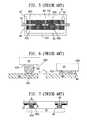
- FIG. 5is a sectional view of a semiconductor package disclosed in U.S. Pat. No. 5,677,567;
- FIG. 6is a schematic diagram showing a process of reflowing solder bump on a conventional lead frame
- FIG. 7is a sectional view of a semiconductor package disclosed in U.S. Pat. No. 6,060,769.
- FIGS. 1 - 4Three preferred embodiments of the semiconductor package of the invention are fully described with reference to FIGS. 1 - 4 as follows.
- a QFN semiconductor packageis exemplified herewith for its practicality in which a die pad is electrically connected directly to external devices.
- a semiconductor package 1 of a first embodiment of the inventioncomprises: a lead frame 10 having a die pad 11 and a plurality of leads 12 surrounding the die pad 11 , wherein the die pad 11 is elevated in position with a pre-determined height difference relative to than the leads 12 ; at least one semiconductor chip 13 mounted on the leads 12 via a plurality of solder bumps 14 in a manner that an active surface 130 of the semiconductor chip 13 faces towards the die pad 11 ; a non-conductive thermal adhesive 112 applied on the die pad 11 for adhering the semiconductor chip 13 to the die pad 11 ; and an encapsulant 15 formed on the lead frame 10 for encapsulating the semiconductor chip 13 .
- the lead frame 10comprises the die pad 11 and the plurality of leads 12 surrounding the die pad 11 , wherein the die pad 11 has a chip carrying surface 110 , and the leads 12 have a lead top surface 120 .
- the lead frame 10is made of a metallic material such as copper or iron/nickel alloy.
- the die pad 11is punched at a central position to form a protruding portion 111 having a height higher than the leads 12 , wherein the chip carrying surface 110 of the protruding portion 111 is spaced from the lead top surface 120 by a height difference not exceeding the original height of the solder bumps (not shown) prior to being reflowed, but designed according to predetermined collapse degree of the solder bumps.
- the lead top surface 120there is further defined at least one contact portion 121 for bonding the corresponding solder bumps (not shown) thereto. Since the copper-made leads 12 are good in solderability and wetability, thus an additional layer of silver, nickel or the like is not necessarily plated on the contact portion 121 .
- a nonconductive thermal adhesive(designated by a reference numeral 112 shown in FIG. 2C) is applied on the chip carrying surface 110 of the protruding portion 111 of the die pad 11 , and a flip-chip process can then be performed.
- the semiconductor chip 13has an active surface 130 disposed with a plurality of electronic circuits and electronic components thereon, and an opposing non-active surface 131 , wherein a plurality of bonding pads 132 are formed on the active surface 130 for bonding the plurality of solder bumps 14 thereto, which are made of soft metallic solder such as tin 63/lead 37 alloy having a low melting point. Then, the semiconductor chip 13 implanted with the solder bumps 14 thereon is mounted on the lead top surface 120 in a manner that, the active surface 130 of the semiconductor chip 13 faces towards the die pad 11 , and each of the solder bumps 14 is attached to the corresponding contact portion 121 .
- the protruding height H 2 of the protruding portion 111 of the die pad 11is smaller than the vertical height H 1 of the solder bumps 14 , thus a cavity W is formed between the semiconductor chip 13 and the protruding portion 111 of the die pad 11 .
- the semiconductor chip 13is substantially suspended above the non-conductive thermal adhesive 112 prior to performing a reflow process.
- the soft solder bumps 14 having a low melting pointstart to melt and collapse, and the semiconductor chip 13 gradually move downwardly due to gravity of its weight. Further, due to the good wetability of the leads 12 , the solder bumps 14 can keep collapsing, making the chip 13 continuously move downwardly until coming into contact with the non-conductive thermal adhesive 112 . At this time, the chip 13 is impeded to further move downwardly by the protruding portion 111 of the die pad 11 , thereby forcing the solder bumps 14 to stop collapsing to be maintained with a certain height.
- the chip 13can be spaced from the leads 12 by a proper distance without detrimentally affecting subsequent processes in fabrication, and the bonding between the solder bumps 14 and the leads 12 can be assured in strength without becoming brittle due to over-collapsing of the solder bumps 14 .
- the semiconductor chip 13is attached to the chip carrying surface 110 of the die pad 11 via the non-conductive thermal adhesive 112 , and heat generated in operation of the chip 13 can be dissipated quickly through the die pad 11 good in thermal conductivity. This therefore helps improve heat dissipation for the semiconductor package and maintain the chip performance.
- a die pad of a lead frameis formed with a protruding portion by using a punching method.
- leads 22 of a lead framecan be processed in a half-etching manner to form a plurality of contact portions 222 thereon, allowing solder bumps 24 to be implanted on the contact portions 222 , wherein the contact portions 222 are dimensioned in depth according to predetermined collapse degree of the solder bumps 24 .
- a reflow processas shown in FIG.
- the solder bumps 24melt and collapse, making a semiconductor chip 23 move downwardly; as an active surface 230 of the semiconductor chip 23 abuts a non-conductive thermal adhesive 212 , the chip 23 is stopped from moving by a die pad 21 .
- an appropriate height difference H 3 formed between the die pad 21 and the contact portions 222can function the same as the protruding portion of the die pad depicted in the foregoing first embodiment, so that collapsing of the solder bumps can be effectively controlled.
- a semiconductor package 3 in a third embodiment of the inventionis structurally identical to that in the foregoing first embodiment, with the only difference in a QFP (quad flat package) or TSOP (thin small outline package) is exemplified, in which a plurality of outer leads 32 in J-like or gull wing shape are formed in the semiconductor package 3 .
- QFPquad flat package
- TSOPthin small outline package
- contact portions 322are formed downset to the leads 32 , allowing a chip carrying surface 310 of a die pad 31 to be positioned with an appropriate height difference relative to the leads 32 , wherein the height difference is predetermined according to collapse degree of the solder bumps 34 , so as to reach the same improvements as recited in the foregoing embodiments.
Landscapes
- Physics & Mathematics (AREA)
- Geometry (AREA)
- Condensed Matter Physics & Semiconductors (AREA)
- General Physics & Mathematics (AREA)
- Engineering & Computer Science (AREA)
- Computer Hardware Design (AREA)
- Microelectronics & Electronic Packaging (AREA)
- Power Engineering (AREA)
- Lead Frames For Integrated Circuits (AREA)
- Wire Bonding (AREA)
Abstract
Description
- The present invention relates to semiconductor packages, and more particularly to a semiconductor package, in which a semiconductor chip is mounted in a flip chip manner on a lead frame.[0001]
- A semiconductor device tends to be made in low cost, high performance and high integration, and is also preferably dimensioned with reduction in size and overall thickness thereof, in correspondence to a trend of low-profile electronic products. A QFN (quad-flat non-leaded) semiconductor package is a mainstream conventional product, due to advantages in that the QFN semiconductor package is only slightly larger in dimension than a semiconductor chip mounted therein, and is cost-effectively made in a lead frame based batch manner.[0002]
- For fabricating such a QFN semiconductor package, generally it is first to mount at least one semiconductor chip on a lead frame having a die pad and a plurality of leads; then, a plurality of gold wires are bonded for electrically connecting the chip and the leads; and finally, an encapsulant is formed to encapsulate the chip. However, in the wire bonding process, due to dense distribution of the leads or complicated layout of the chip, wire loops of the gold wires are interlaced, and thus electric interference occurs if the adjacent gold wires are not properly spaced from each other. Moreover, during the formation of the encapsulating, the gold wires with relatively longer wire loops usually cannot sustain impact from mold flow, and therefore encounter problems such as wire sweep or even short circuit if coming into contact with one another.[0003]
- In addition, with the development in fabrication for a flip chip semiconductor package, a technique of reflowing solder bumps onto bonding pads for establishing electrical connection is getting more commonly used. Comparing to the conventional wire bonding process, the implantation of the solder bumps is implemented by using a one-step and self-alignment process, and thus is more cost-effective and less time-consuming. Accordingly, U.S. Pat. No. 5,677,567 titled as “Leads Between Chips Assembly” discloses a flip chip on lead frame technology. As shown in FIG. 5, a semiconductor device[0004]4 comprises a lead frame (not shown), which is made of a metallic material such as copper, and mainly consists of a plurality of
leads 42 variable in length; a plurality ofsemiconductor chips 43 each having anactive surface 430 disposed with a plurality of bonding pads thereon, and anon-active surface 431; a plurality ofsolder bumps 44 implanted on thebonding pads 432, allowing theleads 42 to be reflowed on each of front and back surfaces thereof with one of thechips 43 in a manner that theactive surface 430 of thechip 43 faces theleads 42; and anencapsulant 45 formed on theleads 42 for encapsulating thesemiconductor chips 43. - This technology is therefore characterized in that the[0005]
semiconductor chip 43 is bonded and electrically connected to thecorresponding leads 42 in a flip-chip manner. Thesolder bumps 44 are made of tin/lead alloy (generally in composition of tin63/lead37 alloy which gives a soft characteristic). As such, during the reflow process, as temperature raises to a certain degree, thesolder bumps 44 collapse to become instantly eutectic withcontact regions 421 of theleads 42. This therefore makes an intermetallic compound layer (not shown) formed between thesolder bumps 44 and thecontact regions 421, in an effort to firmly reinforce the bonding between thesolder bumps 44 and theleads 42. The formation of the intermetallic compound is called a wetting process. However, due to good wetability of the copper-made lead frame (not shown), after thesolder bumps 44 are bonded to predetermined positions (i.e. the contact regions421) on theleads 42 of the lead frame, thesolder bumps 44 still keep collapsing and extending outwardly to be spread on theleads 42, as illustrated in FIG. 6. This over-collapsing of thesolder bumps 44 increases in brittleness of the bonding between thesolder bumps 44 and theleads 42, thereby easily resulting in bonding structural cracking or even loss of electrical properties. Further, the excessively deformedsolder bumps 44 also lead to significantly decrease in the height difference between the semiconductor chip and the leads, and this detrimentally affects the implementation of subsequent processes in fabrication. - In order to solve the above-described problems, as shown in FIG. 7, U.S. Pat. No. 6,060,769 titled as “Flip Chip on Leads Device” discloses a technology of forming a[0006]
solder mask 47 on predetermined positions of theleads 42, wherein thesolder mask 47 has at least one opening470 with predetermined size for bonding thesolder bumps 44 thereto. This technology in essence is to utilize the opening size S of thesolder mask 47 for controlling the collapse degree of thesolder bumps 44. As the size S of theopening 470 increases, thesolder bumps 44 can extend outwardly to a greater extent; that is, the larger the collapse degree, the smaller the vertical height h of thesolder bumps 44 correspondingly. Therefore, with the control in the collapse degree of thesolder bumps 44, the height difference between thesemiconductor chip 43 and theleads 42 can be predetermined, thus eliminating the occurrence of the over-collapsing of thesolder bumps 44. - However, the formation of the solder mask on the lead frame employs such as screen printing or photo-lithographic patterning processes, which are quite complex and ineffective in cost, therefore making it difficult to widely implement in practice. In the case of the solder bumps being alternatively made of e.g. tin 5/lead 95 alloy for raising a melting point thereof, allowing the over-collapsing of the solder bumps to be prevented from occurrence, however, such solder bumps generally doubles up the manufacturing cost thereof[0007]
- A primary objective of the present invention is to provide a lead frame and a semiconductor package with the lead frame, in which a die pad is elevated in position with a proper height difference relative to leads, so as to prevent solder bumps from over-collapsing in a die bonding process, and thus assure bonding reliability of the solder bumps in the semiconductor package.[0008]
- Another objective of the invention is to provide a lead frame and a semiconductor package with the lead frame, in which a lead frame good in heat dissipation is employed, allowing heat generated from a semiconductor chip to be quickly dissipated through a die pad of the lead frame after the semiconductor chip is attached to the die pad, so as to improve overall heat dissipating efficiency of the semiconductor package.[0009]
- In accordance with the foregoing and other objectives, a semiconductor package proposed in the present invention comprises: a lead frame made of metal such as copper, and having a die pad and a plurality of leads, wherein the die pad is higher in elevation than the leads, and a height difference formed between the die pad and the leads does not exceed a height of a plurality of solder bumps, and further a plurality of contact portions are pre-defined on the leads for bonding the corresponding solder bumps thereto; a non-conductive thermal adhesive applied on a top surface of the die pad, for adhering a semiconductor chip to the die pad; at least one semiconductor chip attached in a flip chip manner to the contact portions of the leads via the solder bumps; and an encapsulant for encapsulating the semiconductor chip on the lead frame.[0010]
- In a reflow process for heating the foregoing semiconductor package to a certain temperature, the soft solder bumps having a low melting point start to melt and collapse. Due to good wetability of the copper-made lead frame, the solder bumps keep collapsing, making the semiconductor chip move downwardly due to gravity of its weight. When the semiconductor chip descends in elevation to abut the nonconductive thermal adhesive, the die pad stops the chip from moving, thereby forcing the solder bumps to stop collapsing to be maintained with a certain height.[0011]
- With the provision of the height difference between the die pad and the leads for controlling collapse degree of the solder bumps, it is also beneficial for implementing subsequent processes since the chip is properly spaced from the leads. Moreover, as the die pad functions to restrain the solder bumps from keeping collapsing, it eliminates the occurrence of over-collapsing of the solder bumps and bonding brittleness between the solder bumps and the lead frame, so that structural strength and electrical properties can be assured in the semiconductor package.[0012]
- BRIEF DESCRIPTION OF THE DRAWINGS[0013]
- The present invention can be more fully understood by reading the following detailed description of the preferred embodiments, with reference made to the accompanying drawings, wherein:[0014]
- FIG. 1 is a sectional view of a QFN semiconductor package of a first preferred embodiment of the invention;[0015]
- FIG. 2A is a top view of a lead frame used in a semiconductor package of a first preferred embodiment of the invention;[0016]
- FIG. 2B is a sectional schematic view of FIG. 2A cutting along a[0017]
line 2B-2B; - FIGS.[0018]2C-2D are schematic diagrams depicting the fabrication of a semiconductor package of a first preferred embodiment of the invention;
- FIG. 3A is a sectional view of a QFN semiconductor package of a second preferred embodiment of the invention;[0019]
- FIG. 3B is a partially magnified view of a semiconductor package of a second preferred embodiment of the invention;[0020]
- FIG. 4 is a sectional view of a semiconductor package of a third preferred embodiment of the invention;[0021]
- FIG. 5 (PRIOR ART) is a sectional view of a semiconductor package disclosed in U.S. Pat. No. 5,677,567;[0022]
- FIG. 6 (PRIOR ART) is a schematic diagram showing a process of reflowing solder bump on a conventional lead frame; and[0023]
- FIG. 7 (PRIOR ART) is a sectional view of a semiconductor package disclosed in U.S. Pat. No. 6,060,769.[0024]
- Three preferred embodiments of the semiconductor package of the invention are fully described with reference to FIGS.[0025]1-4 as follows. In particular, a QFN semiconductor package is exemplified herewith for its practicality in which a die pad is electrically connected directly to external devices.
- First Preferred Embodiment[0026]
- As shown in FIG. 1, a semiconductor package[0027]1 of a first embodiment of the invention comprises: a
lead frame 10 having adie pad 11 and a plurality ofleads 12 surrounding thedie pad 11, wherein thedie pad 11 is elevated in position with a pre-determined height difference relative to than theleads 12; at least onesemiconductor chip 13 mounted on theleads 12 via a plurality ofsolder bumps 14 in a manner that anactive surface 130 of thesemiconductor chip 13 faces towards thedie pad 11; a non-conductivethermal adhesive 112 applied on thedie pad 11 for adhering thesemiconductor chip 13 to thedie pad 11; and anencapsulant 15 formed on thelead frame 10 for encapsulating thesemiconductor chip 13. - Referring to FIG. 2A (top view) and FIG. 2B (sectional view), the[0028]
lead frame 10 comprises thedie pad 11 and the plurality ofleads 12 surrounding thedie pad 11, wherein thedie pad 11 has achip carrying surface 110, and theleads 12 have a leadtop surface 120. Thelead frame 10 is made of a metallic material such as copper or iron/nickel alloy. By using a conventional punching method, thedie pad 11 is punched at a central position to form a protrudingportion 111 having a height higher than theleads 12, wherein thechip carrying surface 110 of the protrudingportion 111 is spaced from the leadtop surface 120 by a height difference not exceeding the original height of the solder bumps (not shown) prior to being reflowed, but designed according to predetermined collapse degree of the solder bumps. - Moreover, on the lead[0029]
top surface 120 there is further defined at least onecontact portion 121 for bonding the corresponding solder bumps (not shown) thereto. Since the copper-made leads12 are good in solderability and wetability, thus an additional layer of silver, nickel or the like is not necessarily plated on thecontact portion 121. After thelead frame 10 is completely fabricated, a nonconductive thermal adhesive (designated by areference numeral 112 shown in FIG. 2C) is applied on thechip carrying surface 110 of the protrudingportion 111 of thedie pad 11, and a flip-chip process can then be performed. - As shown in FIG. 2C, the[0030]
semiconductor chip 13 has anactive surface 130 disposed with a plurality of electronic circuits and electronic components thereon, and an opposingnon-active surface 131, wherein a plurality ofbonding pads 132 are formed on theactive surface 130 for bonding the plurality of solder bumps14 thereto, which are made of soft metallic solder such as tin 63/lead 37 alloy having a low melting point. Then, thesemiconductor chip 13 implanted with the solder bumps14 thereon is mounted on the leadtop surface 120 in a manner that, theactive surface 130 of thesemiconductor chip 13 faces towards thedie pad 11, and each of the solder bumps14 is attached to thecorresponding contact portion 121. Since the protruding height H2 of the protrudingportion 111 of thedie pad 11 is smaller than the vertical height H1 of the solder bumps14, thus a cavity W is formed between thesemiconductor chip 13 and the protrudingportion 111 of thedie pad 11. As such, thesemiconductor chip 13 is substantially suspended above the non-conductivethermal adhesive 112 prior to performing a reflow process. - However, after temperature raises to a certain degree during the reflow process, as shown in FIG. 2D, the soft solder bumps[0031]14 having a low melting point start to melt and collapse, and the
semiconductor chip 13 gradually move downwardly due to gravity of its weight. Further, due to the good wetability of theleads 12, the solder bumps14 can keep collapsing, making thechip 13 continuously move downwardly until coming into contact with the non-conductivethermal adhesive 112. At this time, thechip 13 is impeded to further move downwardly by the protrudingportion 111 of thedie pad 11, thereby forcing the solder bumps14 to stop collapsing to be maintained with a certain height. Therefore, thechip 13 can be spaced from theleads 12 by a proper distance without detrimentally affecting subsequent processes in fabrication, and the bonding between the solder bumps14 and theleads 12 can be assured in strength without becoming brittle due to over-collapsing of the solder bumps14. - In addition, as a QFN semiconductor package is exemplified in this embodiment of the invention, after completing the reflow process, the[0032]
semiconductor chip 13 is attached to thechip carrying surface 110 of thedie pad 11 via the non-conductivethermal adhesive 112, and heat generated in operation of thechip 13 can be dissipated quickly through thedie pad 11 good in thermal conductivity. This therefore helps improve heat dissipation for the semiconductor package and maintain the chip performance. - Second Preferred Embodiment[0033]
- In the foregoing first embodiment, a die pad of a lead frame is formed with a protruding portion by using a punching method. Alternatively, as shown in FIG. 3A, in a[0034]
semiconductor package 2 of this embodiment, leads22 of a lead frame can be processed in a half-etching manner to form a plurality ofcontact portions 222 thereon, allowing solder bumps24 to be implanted on thecontact portions 222, wherein thecontact portions 222 are dimensioned in depth according to predetermined collapse degree of the solder bumps24. In a reflow process, as shown in FIG. 3B, the solder bumps24 melt and collapse, making asemiconductor chip 23 move downwardly; as anactive surface 230 of thesemiconductor chip 23 abuts a non-conductivethermal adhesive 212, thechip 23 is stopped from moving by adie pad 21. Thus, in the use of the half-etching process, an appropriate height difference H3 formed between thedie pad 21 and thecontact portions 222 can function the same as the protruding portion of the die pad depicted in the foregoing first embodiment, so that collapsing of the solder bumps can be effectively controlled. - Third Preferred Embodiment[0035]
- As shown in FIG. 4, a[0036]
semiconductor package 3 in a third embodiment of the invention is structurally identical to that in the foregoing first embodiment, with the only difference in a QFP (quad flat package) or TSOP (thin small outline package) is exemplified, in which a plurality ofouter leads 32 in J-like or gull wing shape are formed in thesemiconductor package 3. In the use of a punching method,contact portions 322 are formed downset to theleads 32, allowing achip carrying surface 310 of a die pad31 to be positioned with an appropriate height difference relative to theleads 32, wherein the height difference is predetermined according to collapse degree of the solder bumps34, so as to reach the same improvements as recited in the foregoing embodiments. - The invention has been described using exemplary preferred embodiments. However, it is to be understood that the scope of the invention is not limited to the disclosed embodiments. On the contrary, it is intended to cover various modifications and similar arrangements. The scope of the claims, therefore, should be accorded the broadest interpretation so as to encompass all such modifications and similar arrangements.[0037]
Claims (16)
1. A flip chip semiconductor package, comprising:
a lead frame having a die pad and a plurality of leads surrounding the die pad, wherein the die pad is higher in elevation than the leads, and a height difference formed between the die pad and the leads does not exceed a height of a plurality of conductive elements, which electrically connect a semiconductor chip to the leads;
at least one semiconductor chip electrically connected to the leads by the conductive elements; and
an encapsulant for encapsulating the semiconductor chip and the conductive elements on the lead frame.
2. The flip chip semiconductor package ofclaim 1 , wherein the lead frame is made of a solderable metallic material.
3. The flip chip semiconductor package ofclaim 1 , wherein the die pad has a chip carrying surface with a non-conductive thermal adhesive applied thereon.
4. The flip chip semiconductor package ofclaim 1 , wherein a protruding portion is formed at a center position of the die pad.
5. The flip chip semiconductor package ofclaim 1 , wherein a plurality of contact portions are formed in a half-etching manner on a surface of the leads disposed with the conductive elements thereon.
6. The flip chip semiconductor package ofclaim 1 , wherein the conductive elements are made of soft metal with a low melting point.
7. The flip chip semiconductor package ofclaim 1 , wherein the conductive elements are solder bumps.
8. A lead frame, comprising:
a die pad higher in elevation than the rest of the lead frame, and having a surface for mounting a semiconductor chip thereon; and
a plurality of leads surrounding the die pad, and formed with a plurality of contact portions thereon for attaching a plurality of conductive elements thereto.
9. The lead frame ofclaim 8 , wherein the lead frame is made of a solderable metallic material.
10. The lead frame ofclaim 8 , wherein the surface of the die pad is a chip carrying surface applied with a non-conductive thermal adhesive thereon.
11. The lead frame ofclaim 8 , wherein a protruding portion is formed at a central position of the die pad.
12. The lead frame ofclaim 11 , wherein the protruding portion is formed by using a punching method.
13. The lead frame ofclaim 8 , wherein the contact portions are formed in a half-etching manner with a height difference relative to the die pad.
14. The lead frame ofclaim 13 , wherein the height difference is determined according to collapse degree of the conductive elements.
15. The lead frame ofclaim 8 , wherein the conductive elements ad made of soft metal with low melting point.
16. The lead frame ofclaim 8 , wherein the conductive elements are solder bumps.
Priority Applications (1)
| Application Number | Priority Date | Filing Date | Title |
|---|---|---|---|
| US09/973,358US6661087B2 (en) | 2001-10-09 | 2001-10-09 | Lead frame and flip chip semiconductor package with the same |
Applications Claiming Priority (1)
| Application Number | Priority Date | Filing Date | Title |
|---|---|---|---|
| US09/973,358US6661087B2 (en) | 2001-10-09 | 2001-10-09 | Lead frame and flip chip semiconductor package with the same |
Publications (2)
| Publication Number | Publication Date |
|---|---|
| US20030067057A1true US20030067057A1 (en) | 2003-04-10 |
| US6661087B2 US6661087B2 (en) | 2003-12-09 |
Family
ID=29216495
Family Applications (1)
| Application Number | Title | Priority Date | Filing Date |
|---|---|---|---|
| US09/973,358Expired - LifetimeUS6661087B2 (en) | 2001-10-09 | 2001-10-09 | Lead frame and flip chip semiconductor package with the same |
Country Status (1)
| Country | Link |
|---|---|
| US (1) | US6661087B2 (en) |
Cited By (25)
| Publication number | Priority date | Publication date | Assignee | Title |
|---|---|---|---|---|
| US20030193080A1 (en)* | 2002-04-16 | 2003-10-16 | Cabahug Elsie Agdon | Robust leaded molded packages and methods for forming the same |
| US20050093177A1 (en)* | 2003-10-29 | 2005-05-05 | Advanced Semiconductor Engineering, Inc. | Semiconductor package, method for manufacturing the same and lead frame for use in the same |
| US20050224954A1 (en)* | 2004-04-08 | 2005-10-13 | Kelly Michael G | Thermal dissipation in integrated circuit systems |
| US20050266611A1 (en)* | 2004-06-01 | 2005-12-01 | Jack Tu | Flip chip packaging method and flip chip assembly thereof |
| US20060017173A1 (en)* | 2004-07-23 | 2006-01-26 | Siliconware Precision Industries Co., Ltd. | Flip-chip semiconductor package with lead frame and method for fabricating the same |
| US20060145343A1 (en)* | 2004-12-30 | 2006-07-06 | Samsung Electro-Mechanics Co., Ltd. | BGA package having half-etched bonding pad and cut plating line and method of fabricating same |
| US20060192295A1 (en)* | 2004-11-17 | 2006-08-31 | Chippac, Inc. | Semiconductor package flip chip interconnect having spacer |
| US20070108569A1 (en)* | 2005-07-29 | 2007-05-17 | Stats Chippac Ltd. | Integrated circuit package system with interconnect support |
| US20070210392A1 (en)* | 2005-12-08 | 2007-09-13 | Yamaha Corporation | Semiconductor device |
| US20090051027A1 (en)* | 2000-03-13 | 2009-02-26 | Megica Corporation | Method of Manufacture and Identification of Semiconductor Chip Marked For Identification with Internal Marking Indicia and Protection Thereof by Non-black Layer and Device Produced Thereby |
| US20100102459A1 (en)* | 2008-10-29 | 2010-04-29 | Motoaki Satou | Semiconductor device |
| KR100965120B1 (en) | 2009-09-29 | 2010-06-23 | 주식회사 드림 | High reliance lead-frame for led package |
| US8629539B2 (en)* | 2012-01-16 | 2014-01-14 | Allegro Microsystems, Llc | Methods and apparatus for magnetic sensor having non-conductive die paddle |
| CN103594380A (en)* | 2013-10-24 | 2014-02-19 | 天水华天科技股份有限公司 | Manufacturing method for flat-four-side and non-pin package part with soldered ball surface array |
| US20140220738A1 (en)* | 2013-02-04 | 2014-08-07 | Freescale Semiconductor Inc. | Lead frame array package with flip chip die attach |
| US8810023B2 (en)* | 2012-07-06 | 2014-08-19 | Texas Instruments Incorporated | Cantilever packages for sensor MEMS (micro-electro-mechanical system) |
| TWI492425B (en)* | 2012-05-02 | 2015-07-11 | Advanced Semiconductor Eng | Light emitting diode flip chip package structure |
| US20160172274A1 (en)* | 2014-12-16 | 2016-06-16 | Qualcomm Incorporated | System, apparatus, and method for semiconductor package grounds |
| US9411025B2 (en) | 2013-04-26 | 2016-08-09 | Allegro Microsystems, Llc | Integrated circuit package having a split lead frame and a magnet |
| US9494660B2 (en) | 2012-03-20 | 2016-11-15 | Allegro Microsystems, Llc | Integrated circuit package having a split lead frame |
| US9666788B2 (en) | 2012-03-20 | 2017-05-30 | Allegro Microsystems, Llc | Integrated circuit package having a split lead frame |
| US9812588B2 (en) | 2012-03-20 | 2017-11-07 | Allegro Microsystems, Llc | Magnetic field sensor integrated circuit with integral ferromagnetic material |
| US10234513B2 (en) | 2012-03-20 | 2019-03-19 | Allegro Microsystems, Llc | Magnetic field sensor integrated circuit with integral ferromagnetic material |
| US10991644B2 (en) | 2019-08-22 | 2021-04-27 | Allegro Microsystems, Llc | Integrated circuit package having a low profile |
| US20210175372A1 (en)* | 2019-12-09 | 2021-06-10 | Amkor Technology Singapore Holding Pte. Ltd. | Electronic devices and methods of manufacturing electronic devices |
Families Citing this family (24)
| Publication number | Priority date | Publication date | Assignee | Title |
|---|---|---|---|---|
| KR100583494B1 (en)* | 2000-03-25 | 2006-05-24 | 앰코 테크놀로지 코리아 주식회사 | Semiconductor Package |
| AUPR811101A0 (en)* | 2001-10-05 | 2001-10-25 | Talmor, Eyal Mr | Retractable cable assemblies and devices including the same |
| JP3540793B2 (en)* | 2001-12-05 | 2004-07-07 | 松下電器産業株式会社 | Resin-sealed semiconductor device and method of manufacturing the same |
| DE60217059T2 (en)* | 2002-02-18 | 2007-06-21 | Stmicroelectronics S.R.L., Agrate Brianza | Mounting structure for an electronic power integrated circuit, which is formed on a semiconductor chip, and a corresponding manufacturing method |
| US6953711B2 (en)* | 2003-08-11 | 2005-10-11 | Carsem (M) Sdn. Bhd. | Flip chip on lead frame |
| US7138707B1 (en)* | 2003-10-21 | 2006-11-21 | Amkor Technology, Inc. | Semiconductor package including leads and conductive posts for providing increased functionality |
| TWI225700B (en)* | 2003-10-31 | 2004-12-21 | Advanced Semiconductor Eng | Quad flat flip chip package and lead frame |
| US7148086B2 (en)* | 2005-04-28 | 2006-12-12 | Stats Chippac Ltd. | Semiconductor package with controlled solder bump wetting and fabrication method therefor |
| US7169641B2 (en)* | 2005-05-03 | 2007-01-30 | Stats Chippac Ltd. | Semiconductor package with selective underfill and fabrication method therfor |
| US8022512B2 (en)* | 2006-02-28 | 2011-09-20 | Unisem (Mauritus) Holdings Limited | No lead package with heat spreader |
| US7598603B2 (en)* | 2006-03-15 | 2009-10-06 | Infineon Technologies Ag | Electronic component having a power switch with an anode thereof mounted on a die attach region of a heat sink |
| KR100762354B1 (en) | 2006-09-11 | 2007-10-12 | 주식회사 네패스 | Flip Chip Semiconductor Package and Manufacturing Method Thereof |
| US7491625B2 (en)* | 2007-03-26 | 2009-02-17 | National Semiconductor Corporation | Gang flipping for IC packaging |
| US20080237814A1 (en)* | 2007-03-26 | 2008-10-02 | National Semiconductor Corporation | Isolated solder pads |
| US20080241991A1 (en)* | 2007-03-26 | 2008-10-02 | National Semiconductor Corporation | Gang flipping for flip-chip packaging |
| TWI334205B (en)* | 2007-05-14 | 2010-12-01 | Advanced Semiconductor Eng | Package structure and manufacturing method thereof |
| US8018050B2 (en)* | 2007-11-01 | 2011-09-13 | National Semiconductor Corporation | Integrated circuit package with integrated heat sink |
| US8129229B1 (en)* | 2007-11-10 | 2012-03-06 | Utac Thai Limited | Method of manufacturing semiconductor package containing flip-chip arrangement |
| US8084299B2 (en) | 2008-02-01 | 2011-12-27 | Infineon Technologies Ag | Semiconductor device package and method of making a semiconductor device package |
| US8138027B2 (en)* | 2008-03-07 | 2012-03-20 | Stats Chippac, Ltd. | Optical semiconductor device having pre-molded leadframe with window and method therefor |
| US8097944B2 (en)* | 2009-04-30 | 2012-01-17 | Infineon Technologies Ag | Semiconductor device |
| US8390103B2 (en) | 2010-07-12 | 2013-03-05 | Analog Devices, Inc. | Apparatus for integrated circuit packaging |
| CN104465588B (en) | 2013-09-25 | 2018-11-02 | 恩智浦美国有限公司 | Semiconductor package part with stress release and radiator |
| US9679870B2 (en) | 2014-12-10 | 2017-06-13 | Stmicroelectronics Pte Ltd | Integrated circuit device with shaped leads and method of forming the device |
Family Cites Families (4)
| Publication number | Priority date | Publication date | Assignee | Title |
|---|---|---|---|---|
| JPH08116016A (en)* | 1994-10-15 | 1996-05-07 | Toshiba Corp | Lead frame and semiconductor device |
| US5677567A (en) | 1996-06-17 | 1997-10-14 | Micron Technology, Inc. | Leads between chips assembly |
| US5817540A (en) | 1996-09-20 | 1998-10-06 | Micron Technology, Inc. | Method of fabricating flip-chip on leads devices and resulting assemblies |
| US6208020B1 (en)* | 1999-02-24 | 2001-03-27 | Matsushita Electronics Corporation | Leadframe for use in manufacturing a resin-molded semiconductor device |
- 2001
- 2001-10-09USUS09/973,358patent/US6661087B2/ennot_activeExpired - Lifetime
Cited By (54)
| Publication number | Priority date | Publication date | Assignee | Title |
|---|---|---|---|---|
| US20090051027A1 (en)* | 2000-03-13 | 2009-02-26 | Megica Corporation | Method of Manufacture and Identification of Semiconductor Chip Marked For Identification with Internal Marking Indicia and Protection Thereof by Non-black Layer and Device Produced Thereby |
| US7122884B2 (en)* | 2002-04-16 | 2006-10-17 | Fairchild Semiconductor Corporation | Robust leaded molded packages and methods for forming the same |
| US20030193080A1 (en)* | 2002-04-16 | 2003-10-16 | Cabahug Elsie Agdon | Robust leaded molded packages and methods for forming the same |
| US20090236714A1 (en)* | 2002-04-16 | 2009-09-24 | Elsie Agdon Cabahug | Robust leaded molded packages and methods for forming the same |
| US7560311B2 (en) | 2002-04-16 | 2009-07-14 | Fairchild Semiconductor Corporation | Robust leaded molded packages and methods for forming the same |
| US7906837B2 (en) | 2002-04-16 | 2011-03-15 | Fairchild Semiconductor Corporation | Robust leaded molded packages and methods for forming the same |
| US20060231933A1 (en)* | 2002-04-16 | 2006-10-19 | Cabahug Elsie A | Robust leaded molded packages and methods for forming the same |
| US7425755B2 (en)* | 2003-10-29 | 2008-09-16 | Advanced Semiconductor Engineering Inc. | Semiconductor package, method for manufacturing the same and lead frame for use in the same |
| US20050093177A1 (en)* | 2003-10-29 | 2005-05-05 | Advanced Semiconductor Engineering, Inc. | Semiconductor package, method for manufacturing the same and lead frame for use in the same |
| US20050224954A1 (en)* | 2004-04-08 | 2005-10-13 | Kelly Michael G | Thermal dissipation in integrated circuit systems |
| US7868472B2 (en)* | 2004-04-08 | 2011-01-11 | Avago Technologies General Ip (Singapore) Pte. Ltd. | Thermal dissipation in integrated circuit systems |
| US20050266611A1 (en)* | 2004-06-01 | 2005-12-01 | Jack Tu | Flip chip packaging method and flip chip assembly thereof |
| US7170168B2 (en)* | 2004-07-23 | 2007-01-30 | Siliconware Precision Industries Co., Ltd. | Flip-chip semiconductor package with lead frame and method for fabricating the same |
| US20060017173A1 (en)* | 2004-07-23 | 2006-01-26 | Siliconware Precision Industries Co., Ltd. | Flip-chip semiconductor package with lead frame and method for fabricating the same |
| US7880313B2 (en)* | 2004-11-17 | 2011-02-01 | Chippac, Inc. | Semiconductor flip chip package having substantially non-collapsible spacer |
| US20060192295A1 (en)* | 2004-11-17 | 2006-08-31 | Chippac, Inc. | Semiconductor package flip chip interconnect having spacer |
| US20060145343A1 (en)* | 2004-12-30 | 2006-07-06 | Samsung Electro-Mechanics Co., Ltd. | BGA package having half-etched bonding pad and cut plating line and method of fabricating same |
| US7901996B2 (en) | 2005-07-29 | 2011-03-08 | Stats Chippac Ltd. | Integrated circuit package system with interconnection support and method of manufacture thereof |
| US7563647B2 (en)* | 2005-07-29 | 2009-07-21 | Stats Chippac Ltd. | Integrated circuit package system with interconnect support |
| US20090250798A1 (en)* | 2005-07-29 | 2009-10-08 | Bathan Henry D | Integrated circuit package system with interconnect support |
| US20070108569A1 (en)* | 2005-07-29 | 2007-05-17 | Stats Chippac Ltd. | Integrated circuit package system with interconnect support |
| US7560811B2 (en)* | 2005-12-08 | 2009-07-14 | Yamaha Corporation | Semiconductor device |
| US20090096041A1 (en)* | 2005-12-08 | 2009-04-16 | Yamaha Corporation | Semiconductor device |
| US20070210392A1 (en)* | 2005-12-08 | 2007-09-13 | Yamaha Corporation | Semiconductor device |
| US20100102459A1 (en)* | 2008-10-29 | 2010-04-29 | Motoaki Satou | Semiconductor device |
| WO2011040737A3 (en)* | 2009-09-29 | 2011-07-07 | 주식회사 드림 | Highly reliable lead frame for an led package |
| KR100965120B1 (en) | 2009-09-29 | 2010-06-23 | 주식회사 드림 | High reliance lead-frame for led package |
| US8629539B2 (en)* | 2012-01-16 | 2014-01-14 | Allegro Microsystems, Llc | Methods and apparatus for magnetic sensor having non-conductive die paddle |
| US9620705B2 (en) | 2012-01-16 | 2017-04-11 | Allegro Microsystems, Llc | Methods and apparatus for magnetic sensor having non-conductive die paddle |
| US10333055B2 (en) | 2012-01-16 | 2019-06-25 | Allegro Microsystems, Llc | Methods for magnetic sensor having non-conductive die paddle |
| US9299915B2 (en) | 2012-01-16 | 2016-03-29 | Allegro Microsystems, Llc | Methods and apparatus for magnetic sensor having non-conductive die paddle |
| US11828819B2 (en) | 2012-03-20 | 2023-11-28 | Allegro Microsystems, Llc | Magnetic field sensor integrated circuit with integral ferromagnetic material |
| US10916665B2 (en) | 2012-03-20 | 2021-02-09 | Allegro Microsystems, Llc | Magnetic field sensor integrated circuit with an integrated coil |
| US11444209B2 (en) | 2012-03-20 | 2022-09-13 | Allegro Microsystems, Llc | Magnetic field sensor integrated circuit with an integrated coil enclosed with a semiconductor die by a mold material |
| US11677032B2 (en) | 2012-03-20 | 2023-06-13 | Allegro Microsystems, Llc | Sensor integrated circuit with integrated coil and element in central region of mold material |
| US10230006B2 (en) | 2012-03-20 | 2019-03-12 | Allegro Microsystems, Llc | Magnetic field sensor integrated circuit with an electromagnetic suppressor |
| US10234513B2 (en) | 2012-03-20 | 2019-03-19 | Allegro Microsystems, Llc | Magnetic field sensor integrated circuit with integral ferromagnetic material |
| US9494660B2 (en) | 2012-03-20 | 2016-11-15 | Allegro Microsystems, Llc | Integrated circuit package having a split lead frame |
| US11961920B2 (en) | 2012-03-20 | 2024-04-16 | Allegro Microsystems, Llc | Integrated circuit package with magnet having a channel |
| US9666788B2 (en) | 2012-03-20 | 2017-05-30 | Allegro Microsystems, Llc | Integrated circuit package having a split lead frame |
| US9812588B2 (en) | 2012-03-20 | 2017-11-07 | Allegro Microsystems, Llc | Magnetic field sensor integrated circuit with integral ferromagnetic material |
| TWI492425B (en)* | 2012-05-02 | 2015-07-11 | Advanced Semiconductor Eng | Light emitting diode flip chip package structure |
| CN104411619A (en)* | 2012-07-06 | 2015-03-11 | 德克萨斯仪器股份有限公司 | Sensor MEMS device cantilever packaging |
| US8810023B2 (en)* | 2012-07-06 | 2014-08-19 | Texas Instruments Incorporated | Cantilever packages for sensor MEMS (micro-electro-mechanical system) |
| US8969139B2 (en)* | 2013-02-04 | 2015-03-03 | Freescale Semiconductor, Inc. | Lead frame array package with flip chip die attach |
| US20140220738A1 (en)* | 2013-02-04 | 2014-08-07 | Freescale Semiconductor Inc. | Lead frame array package with flip chip die attach |
| US9411025B2 (en) | 2013-04-26 | 2016-08-09 | Allegro Microsystems, Llc | Integrated circuit package having a split lead frame and a magnet |
| CN103594380A (en)* | 2013-10-24 | 2014-02-19 | 天水华天科技股份有限公司 | Manufacturing method for flat-four-side and non-pin package part with soldered ball surface array |
| US20160172274A1 (en)* | 2014-12-16 | 2016-06-16 | Qualcomm Incorporated | System, apparatus, and method for semiconductor package grounds |
| US10991644B2 (en) | 2019-08-22 | 2021-04-27 | Allegro Microsystems, Llc | Integrated circuit package having a low profile |
| US20210175372A1 (en)* | 2019-12-09 | 2021-06-10 | Amkor Technology Singapore Holding Pte. Ltd. | Electronic devices and methods of manufacturing electronic devices |
| US11437526B2 (en)* | 2019-12-09 | 2022-09-06 | Amkor Technology Singapore Holding Pte. Ltd. | Electronic devices having a sensor and a translucent mold compound and methods of manufacturing electronic devices |
| US20220393039A1 (en)* | 2019-12-09 | 2022-12-08 | Amkor Technology Singapore Holding Pte. Ltd. | Electronic devices and methods of manufacturing electronic devices |
| US12176443B2 (en)* | 2019-12-09 | 2024-12-24 | Amkor Technology Singapore Holding Pte. Ltd. | Electronic sensor devices and methods of manufacturing electronic sensor devices |
Also Published As
| Publication number | Publication date |
|---|---|
| US6661087B2 (en) | 2003-12-09 |
Similar Documents
| Publication | Publication Date | Title |
|---|---|---|
| US6661087B2 (en) | Lead frame and flip chip semiconductor package with the same | |
| US7274088B2 (en) | Flip-chip semiconductor package with lead frame as chip carrier and fabrication method thereof | |
| US6764880B2 (en) | Semiconductor package and fabricating method thereof | |
| US7253508B2 (en) | Semiconductor package with a flip chip on a solder-resist leadframe | |
| KR100239406B1 (en) | Surface mounted semiconductor package and method of manufacturing the same | |
| US9029991B2 (en) | Semiconductor packages with reduced solder voiding | |
| KR20070074489A (en) | Semiconductor device and manufacturing method thereof | |
| US20040238923A1 (en) | Surface-mount-enhanced lead frame and method for fabricating semiconductor package with the same | |
| US20230411258A1 (en) | Semiconductor device and corresponding method | |
| US6501160B1 (en) | Semiconductor device and a method of manufacturing the same and a mount structure | |
| JP4547086B2 (en) | Semiconductor device | |
| US20020182773A1 (en) | Method for bonding inner leads of leadframe to substrate | |
| JP2007059485A (en) | Semiconductor device, substrate and method of manufacturing semiconductor device | |
| JP4243270B2 (en) | Manufacturing method of semiconductor device | |
| KR0119757Y1 (en) | Semiconductor package | |
| EP4579734A1 (en) | Hybrid ball/bump and wirebond semiconductor device packaging | |
| KR100460048B1 (en) | Bump chip carrier package and method for fabricating the same | |
| US20070054438A1 (en) | Carrier-free semiconductor package with stand-off member and fabrication method thereof | |
| JP2001135767A (en) | Semiconductor device and method of manufacturing the same | |
| KR20020029990A (en) | Semiconductor package and manufacturing method thereof comprising substrate with mounting lead | |
| JP3215505B2 (en) | Standard lead frame and method of manufacturing lead frame using this standard lead frame | |
| CN100334721C (en) | Flip Chip Semiconductor Package | |
| JP2000150761A (en) | Resin-sealed semiconductor device and method of manufacturing the same | |
| JPH11195743A (en) | Semiconductor device and manufacturing method thereof | |
| JP2011155293A (en) | Method of manufacturing semiconductor device |
Legal Events
| Date | Code | Title | Description |
|---|---|---|---|
| AS | Assignment | Owner name:SILICONWARE PRECISION INDUSTRIES CO., LTD., TAIWAN Free format text:ASSIGNMENT OF ASSIGNORS INTEREST;ASSIGNOR:WU, CHI CHUAN;REEL/FRAME:012249/0024 Effective date:20010720 | |
| STCF | Information on status: patent grant | Free format text:PATENTED CASE | |
| FPAY | Fee payment | Year of fee payment:4 | |
| FPAY | Fee payment | Year of fee payment:8 | |
| FPAY | Fee payment | Year of fee payment:12 |