US20030059987A1 - Inkjet-fabricated integrated circuits - Google Patents
Inkjet-fabricated integrated circuitsDownload PDFInfo
- Publication number
- US20030059987A1 US20030059987A1US10/175,954US17595402AUS2003059987A1US 20030059987 A1US20030059987 A1US 20030059987A1US 17595402 AUS17595402 AUS 17595402AUS 2003059987 A1US2003059987 A1US 2003059987A1
- Authority
- US
- United States
- Prior art keywords
- ink
- transistors
- jet printing
- substrate
- devices
- Prior art date
- Legal status (The legal status is an assumption and is not a legal conclusion. Google has not performed a legal analysis and makes no representation as to the accuracy of the status listed.)
- Granted
Links
- 238000000034methodMethods0.000claimsabstractdescription124
- 238000007641inkjet printingMethods0.000claimsabstractdescription67
- 239000000758substrateSubstances0.000claimsdescription103
- 229920000642polymerPolymers0.000claimsdescription78
- 239000002904solventSubstances0.000claimsdescription78
- 238000000151depositionMethods0.000claimsdescription71
- 239000000463materialSubstances0.000claimsdescription58
- 230000008021depositionEffects0.000claimsdescription54
- 239000004020conductorSubstances0.000claimsdescription30
- 238000007639printingMethods0.000claimsdescription30
- 229920001400block copolymerPolymers0.000claimsdescription14
- 239000000178monomerSubstances0.000claimsdescription12
- 230000003287optical effectEffects0.000claimsdescription12
- 238000012545processingMethods0.000claimsdescription10
- 239000007788liquidSubstances0.000claimsdescription9
- 239000002861polymer materialSubstances0.000claimsdescription8
- 229920001940conductive polymerPolymers0.000claimsdescription7
- 239000002019doping agentSubstances0.000claimsdescription7
- 229920000547conjugated polymerPolymers0.000claimsdescription6
- 125000000843phenylene groupChemical groupC1(=C(C=CC=C1)*)*0.000claimsdescription6
- 239000003990capacitorSubstances0.000claimsdescription5
- PJULCNAVAGQLAT-UHFFFAOYSA-Nindeno[2,1-a]fluoreneChemical classC1=CC=C2C=C3C4=CC5=CC=CC=C5C4=CC=C3C2=C1PJULCNAVAGQLAT-UHFFFAOYSA-N0.000claimsdescription4
- 150000003577thiophenesChemical class0.000claimsdescription4
- 125000005259triarylamine groupChemical group0.000claimsdescription4
- 239000011810insulating materialSubstances0.000claimsdescription3
- 230000001846repelling effectEffects0.000claimsdescription3
- UELITFHSCLAHKR-UHFFFAOYSA-Nacibenzolar-S-methylChemical compoundCSC(=O)C1=CC=CC2=C1SN=N2UELITFHSCLAHKR-UHFFFAOYSA-N0.000claimsdescription2
- 239000012777electrically insulating materialSubstances0.000claimsdescription2
- 125000003983fluorenyl groupChemical classC1(=CC=CC=2C3=CC=CC=C3CC12)*0.000claims1
- 239000010410layerSubstances0.000description204
- 229920001609Poly(3,4-ethylenedioxythiophene)Polymers0.000description54
- 229920001665Poly-4-vinylphenolPolymers0.000description36
- 229920001721polyimidePolymers0.000description35
- 239000004642PolyimideSubstances0.000description34
- 239000000243solutionSubstances0.000description34
- OKKJLVBELUTLKV-UHFFFAOYSA-NMethanolChemical groupOCOKKJLVBELUTLKV-UHFFFAOYSA-N0.000description33
- 238000009792diffusion processMethods0.000description33
- 230000004888barrier functionEffects0.000description25
- 239000011521glassSubstances0.000description20
- 230000008569processEffects0.000description19
- XLYOFNOQVPJJNP-UHFFFAOYSA-NwaterSubstancesOXLYOFNOQVPJJNP-UHFFFAOYSA-N0.000description18
- 238000004519manufacturing processMethods0.000description16
- 238000000059patterningMethods0.000description16
- KFZMGEQAYNKOFK-UHFFFAOYSA-NIsopropanolChemical compoundCC(C)OKFZMGEQAYNKOFK-UHFFFAOYSA-N0.000description15
- 230000002209hydrophobic effectEffects0.000description15
- 239000004065semiconductorSubstances0.000description15
- 230000015572biosynthetic processEffects0.000description13
- 230000004048modificationEffects0.000description13
- 238000012986modificationMethods0.000description13
- 238000012546transferMethods0.000description13
- 239000002798polar solventSubstances0.000description12
- 230000000694effectsEffects0.000description11
- 239000010408filmSubstances0.000description11
- 239000011159matrix materialSubstances0.000description11
- 230000037230mobilityEffects0.000description11
- 239000002094self assembled monolayerSubstances0.000description10
- 239000013545self-assembled monolayerSubstances0.000description10
- 229920002120photoresistant polymerPolymers0.000description9
- 229920006113non-polar polymerPolymers0.000description8
- 229920000301poly(3-hexylthiophene-2,5-diyl) polymerPolymers0.000description8
- 239000008096xyleneSubstances0.000description8
- 230000006399behaviorEffects0.000description7
- 230000005661hydrophobic surfaceEffects0.000description7
- 229920006112polar polymerPolymers0.000description7
- LFQSCWFLJHTTHZ-UHFFFAOYSA-NEthanolChemical compoundCCOLFQSCWFLJHTTHZ-UHFFFAOYSA-N0.000description6
- CTQNGGLPUBDAKN-UHFFFAOYSA-NO-XyleneChemical compoundCC1=CC=CC=C1CCTQNGGLPUBDAKN-UHFFFAOYSA-N0.000description6
- QVGXLLKOCUKJST-UHFFFAOYSA-Natomic oxygenChemical compound[O]QVGXLLKOCUKJST-UHFFFAOYSA-N0.000description6
- 239000002800charge carrierSubstances0.000description6
- 238000004090dissolutionMethods0.000description6
- 238000001035dryingMethods0.000description6
- 239000010931goldSubstances0.000description6
- 230000003993interactionEffects0.000description6
- 239000000203mixtureSubstances0.000description6
- 239000001301oxygenSubstances0.000description6
- 229910052760oxygenInorganic materials0.000description6
- 239000004926polymethyl methacrylateSubstances0.000description6
- 230000008961swellingEffects0.000description6
- 238000009736wettingMethods0.000description6
- 238000000137annealingMethods0.000description5
- 239000002322conducting polymerSubstances0.000description5
- 238000005516engineering processMethods0.000description5
- 238000001704evaporationMethods0.000description5
- 125000000524functional groupChemical group0.000description5
- PCHJSUWPFVWCPO-UHFFFAOYSA-NgoldChemical compound[Au]PCHJSUWPFVWCPO-UHFFFAOYSA-N0.000description5
- 229910052737goldInorganic materials0.000description5
- 230000005660hydrophilic surfaceEffects0.000description5
- 125000002887hydroxy groupChemical group[H]O*0.000description5
- 239000012535impuritySubstances0.000description5
- 238000002347injectionMethods0.000description5
- 239000007924injectionSubstances0.000description5
- 238000005259measurementMethods0.000description5
- 238000000879optical micrographMethods0.000description5
- 229920003023plasticPolymers0.000description5
- 239000004033plasticSubstances0.000description5
- 241000894007speciesSpecies0.000description5
- 230000007480spreadingEffects0.000description5
- 238000003892spreadingMethods0.000description5
- LRHPLDYGYMQRHN-UHFFFAOYSA-NN-ButanolChemical compoundCCCCOLRHPLDYGYMQRHN-UHFFFAOYSA-N0.000description4
- SECXISVLQFMRJM-UHFFFAOYSA-NN-MethylpyrrolidoneChemical compoundCN1CCCC1=OSECXISVLQFMRJM-UHFFFAOYSA-N0.000description4
- 229920000144PEDOT:PSSPolymers0.000description4
- 239000004793PolystyreneSubstances0.000description4
- 230000008901benefitEffects0.000description4
- 238000010017direct printingMethods0.000description4
- 239000012212insulatorSubstances0.000description4
- 239000012299nitrogen atmosphereSubstances0.000description4
- 239000012454non-polar solventSubstances0.000description4
- 230000002829reductive effectEffects0.000description4
- 239000007787solidSubstances0.000description4
- 238000010129solution processingMethods0.000description4
- 239000010409thin filmSubstances0.000description4
- CSCPPACGZOOCGX-UHFFFAOYSA-NAcetoneChemical compoundCC(C)=OCSCPPACGZOOCGX-UHFFFAOYSA-N0.000description3
- 239000004372Polyvinyl alcoholSubstances0.000description3
- 238000010521absorption reactionMethods0.000description3
- 239000012298atmosphereSubstances0.000description3
- 230000003247decreasing effectEffects0.000description3
- 230000008020evaporationEffects0.000description3
- 230000005669field effectEffects0.000description3
- 150000002220fluorenesChemical class0.000description3
- 238000009472formulationMethods0.000description3
- 230000006870functionEffects0.000description3
- 229920001519homopolymerPolymers0.000description3
- 150000002500ionsChemical class0.000description3
- 238000002156mixingMethods0.000description3
- 229920002098polyfluorenePolymers0.000description3
- 229920002223polystyrenePolymers0.000description3
- 229920000123polythiophenePolymers0.000description3
- 229940068984polyvinyl alcoholDrugs0.000description3
- 235000019422polyvinyl alcoholNutrition0.000description3
- 229920002451polyvinyl alcoholPolymers0.000description3
- 230000003595spectral effectEffects0.000description3
- IJGRMHOSHXDMSA-UHFFFAOYSA-NAtomic nitrogenChemical groupN#NIJGRMHOSHXDMSA-UHFFFAOYSA-N0.000description2
- OAKJQQAXSVQMHS-UHFFFAOYSA-NHydrazineChemical compoundNNOAKJQQAXSVQMHS-UHFFFAOYSA-N0.000description2
- VYPSYNLAJGMNEJ-UHFFFAOYSA-NSilicium dioxideChemical compoundO=[Si]=OVYPSYNLAJGMNEJ-UHFFFAOYSA-N0.000description2
- 238000009825accumulationMethods0.000description2
- 230000009471actionEffects0.000description2
- 150000001298alcoholsChemical class0.000description2
- 125000003545alkoxy groupChemical group0.000description2
- 239000004411aluminiumSubstances0.000description2
- 229910052782aluminiumInorganic materials0.000description2
- XAGFODPZIPBFFR-UHFFFAOYSA-NaluminiumChemical compound[Al]XAGFODPZIPBFFR-UHFFFAOYSA-N0.000description2
- 229910021417amorphous siliconInorganic materials0.000description2
- 238000009835boilingMethods0.000description2
- 230000015556catabolic processEffects0.000description2
- 239000011248coating agentSubstances0.000description2
- 238000000576coating methodMethods0.000description2
- 229920001577copolymerPolymers0.000description2
- 230000005574cross-species transmissionEffects0.000description2
- 230000007423decreaseEffects0.000description2
- 238000006731degradation reactionMethods0.000description2
- DMBHHRLKUKUOEG-UHFFFAOYSA-NdiphenylamineChemical compoundC=1C=CC=CC=1NC1=CC=CC=C1DMBHHRLKUKUOEG-UHFFFAOYSA-N0.000description2
- 230000007613environmental effectEffects0.000description2
- 238000005530etchingMethods0.000description2
- 229920002457flexible plasticPolymers0.000description2
- 239000001257hydrogenSubstances0.000description2
- 229910052739hydrogenInorganic materials0.000description2
- 238000001540jet depositionMethods0.000description2
- 229920002521macromoleculePolymers0.000description2
- 229910052751metalInorganic materials0.000description2
- 239000002184metalSubstances0.000description2
- 238000000813microcontact printingMethods0.000description2
- 239000003960organic solventSubstances0.000description2
- 238000003909pattern recognitionMethods0.000description2
- 238000009832plasma treatmentMethods0.000description2
- 239000003495polar organic solventSubstances0.000description2
- 238000007650screen-printingMethods0.000description2
- 238000004528spin coatingMethods0.000description2
- 230000003746surface roughnessEffects0.000description2
- 239000000725suspensionSubstances0.000description2
- 238000012360testing methodMethods0.000description2
- 150000003738xylenesChemical class0.000description2
- FNQJDLTXOVEEFB-UHFFFAOYSA-N1,2,3-benzothiadiazoleChemical classC1=CC=C2SN=NC2=C1FNQJDLTXOVEEFB-UHFFFAOYSA-N0.000description1
- OGGKVJMNFFSDEV-UHFFFAOYSA-N3-methyl-n-[4-[4-(n-(3-methylphenyl)anilino)phenyl]phenyl]-n-phenylanilineChemical compoundCC1=CC=CC(N(C=2C=CC=CC=2)C=2C=CC(=CC=2)C=2C=CC(=CC=2)N(C=2C=CC=CC=2)C=2C=C(C)C=CC=2)=C1OGGKVJMNFFSDEV-UHFFFAOYSA-N0.000description1
- DKPFZGUDAPQIHT-UHFFFAOYSA-NButyl acetateNatural productsCCCCOC(C)=ODKPFZGUDAPQIHT-UHFFFAOYSA-N0.000description1
- 239000005046ChlorosilaneSubstances0.000description1
- JSHDAORXSNJOBA-UHFFFAOYSA-NIsopropyl hexanoateChemical compoundCCCCCC(=O)OC(C)CJSHDAORXSNJOBA-UHFFFAOYSA-N0.000description1
- 229920005439Perspex®Polymers0.000description1
- 206010034972Photosensitivity reactionDiseases0.000description1
- NINIDFKCEFEMDL-UHFFFAOYSA-NSulfurChemical group[S]NINIDFKCEFEMDL-UHFFFAOYSA-N0.000description1
- 239000005864SulphurSubstances0.000description1
- 238000000862absorption spectrumMethods0.000description1
- 230000002378acidificating effectEffects0.000description1
- 239000000853adhesiveSubstances0.000description1
- 230000001070adhesive effectEffects0.000description1
- 125000000217alkyl groupChemical group0.000description1
- 125000005233alkylalcohol groupChemical group0.000description1
- 230000000903blocking effectEffects0.000description1
- UHYPYGJEEGLRJD-UHFFFAOYSA-Ncadmium(2+);selenium(2-)Chemical compound[Se-2].[Cd+2]UHYPYGJEEGLRJD-UHFFFAOYSA-N0.000description1
- 238000006243chemical reactionMethods0.000description1
- KOPOQZFJUQMUML-UHFFFAOYSA-NchlorosilaneChemical compoundCl[SiH3]KOPOQZFJUQMUML-UHFFFAOYSA-N0.000description1
- 229910052681coesiteInorganic materials0.000description1
- 229920000891common polymerPolymers0.000description1
- 229910052906cristobaliteInorganic materials0.000description1
- 238000004132cross linkingMethods0.000description1
- 230000002950deficientEffects0.000description1
- 238000005137deposition processMethods0.000description1
- 238000010586diagramMethods0.000description1
- RAABOESOVLLHRU-UHFFFAOYSA-NdiazeneChemical classN=NRAABOESOVLLHRU-UHFFFAOYSA-N0.000description1
- 239000003989dielectric materialSubstances0.000description1
- 238000007865dilutingMethods0.000description1
- 238000003618dip coatingMethods0.000description1
- 230000005684electric fieldEffects0.000description1
- 238000010292electrical insulationMethods0.000description1
- 239000007772electrode materialSubstances0.000description1
- 238000009713electroplatingMethods0.000description1
- 230000008713feedback mechanismEffects0.000description1
- 238000011049fillingMethods0.000description1
- 125000001153fluoro groupChemical groupF*0.000description1
- 238000007306functionalization reactionMethods0.000description1
- 125000005842heteroatomChemical group0.000description1
- FUZZWVXGSFPDMH-UHFFFAOYSA-Nhexanoic acidChemical compoundCCCCCC(O)=OFUZZWVXGSFPDMH-UHFFFAOYSA-N0.000description1
- 238000005286illuminationMethods0.000description1
- 230000006872improvementEffects0.000description1
- 238000010348incorporationMethods0.000description1
- AMGQUBHHOARCQH-UHFFFAOYSA-Nindium;oxotinChemical compound[In].[Sn]=OAMGQUBHHOARCQH-UHFFFAOYSA-N0.000description1
- 239000010954inorganic particleSubstances0.000description1
- 238000003780insertionMethods0.000description1
- 230000037431insertionEffects0.000description1
- 238000002955isolationMethods0.000description1
- 239000004973liquid crystal related substanceSubstances0.000description1
- 230000007774longtermEffects0.000description1
- 230000007246mechanismEffects0.000description1
- 150000002739metalsChemical class0.000description1
- ARYZCSRUUPFYMY-UHFFFAOYSA-NmethoxysilaneChemical groupCO[SiH3]ARYZCSRUUPFYMY-UHFFFAOYSA-N0.000description1
- 238000001000micrographMethods0.000description1
- 239000002105nanoparticleSubstances0.000description1
- 229910052757nitrogenChemical group0.000description1
- 230000005693optoelectronicsEffects0.000description1
- 238000012856packingMethods0.000description1
- 125000002080perylenyl groupChemical groupC1(=CC=C2C=CC=C3C4=CC=CC5=CC=CC(C1=C23)=C45)*0.000description1
- 238000000206photolithographyMethods0.000description1
- 230000036211photosensitivityEffects0.000description1
- 239000002985plastic filmSubstances0.000description1
- 238000007747platingMethods0.000description1
- 229920000767polyanilinePolymers0.000description1
- 229920000128polypyrrolePolymers0.000description1
- 238000012805post-processingMethods0.000description1
- 239000002243precursorSubstances0.000description1
- 238000001314profilometryMethods0.000description1
- 230000000750progressive effectEffects0.000description1
- LLHKCFNBLRBOGN-UHFFFAOYSA-Npropylene glycol methyl ether acetateChemical compoundCOCC(C)OC(C)=OLLHKCFNBLRBOGN-UHFFFAOYSA-N0.000description1
- 238000004080punchingMethods0.000description1
- 238000010791quenchingMethods0.000description1
- 230000000171quenching effectEffects0.000description1
- 230000005855radiationEffects0.000description1
- 230000009467reductionEffects0.000description1
- 239000013074reference sampleSubstances0.000description1
- 239000003870refractory metalSubstances0.000description1
- 238000009877renderingMethods0.000description1
- 230000002940repellentEffects0.000description1
- 239000005871repellentSubstances0.000description1
- 239000013557residual solventSubstances0.000description1
- 230000002441reversible effectEffects0.000description1
- 239000000523sampleSubstances0.000description1
- 238000007789sealingMethods0.000description1
- 239000000377silicon dioxideSubstances0.000description1
- 150000003384small moleculesChemical class0.000description1
- 239000011877solvent mixtureSubstances0.000description1
- 229910052682stishoviteInorganic materials0.000description1
- 239000000126substanceSubstances0.000description1
- 230000001629suppressionEffects0.000description1
- 239000004094surface-active agentSubstances0.000description1
- 229910052715tantalumInorganic materials0.000description1
- GUVRBAGPIYLISA-UHFFFAOYSA-Ntantalum atomChemical compound[Ta]GUVRBAGPIYLISA-UHFFFAOYSA-N0.000description1
- 230000007704transitionEffects0.000description1
- 238000013519translationMethods0.000description1
- PYJJCSYBSYXGQQ-UHFFFAOYSA-Ntrichloro(octadecyl)silaneChemical compoundCCCCCCCCCCCCCCCCCC[Si](Cl)(Cl)ClPYJJCSYBSYXGQQ-UHFFFAOYSA-N0.000description1
- 229910052905tridymiteInorganic materials0.000description1
- JLGNHOJUQFHYEZ-UHFFFAOYSA-Ntrimethoxy(3,3,3-trifluoropropyl)silaneChemical groupCO[Si](OC)(OC)CCC(F)(F)FJLGNHOJUQFHYEZ-UHFFFAOYSA-N0.000description1
- WFKWXMTUELFFGS-UHFFFAOYSA-NtungstenChemical compound[W]WFKWXMTUELFFGS-UHFFFAOYSA-N0.000description1
- 229910052721tungstenInorganic materials0.000description1
- 239000010937tungstenSubstances0.000description1
- 238000001771vacuum depositionMethods0.000description1
- 238000012795verificationMethods0.000description1
Images


Classifications
- B—PERFORMING OPERATIONS; TRANSPORTING
- B82—NANOTECHNOLOGY
- B82Y—SPECIFIC USES OR APPLICATIONS OF NANOSTRUCTURES; MEASUREMENT OR ANALYSIS OF NANOSTRUCTURES; MANUFACTURE OR TREATMENT OF NANOSTRUCTURES
- B82Y10/00—Nanotechnology for information processing, storage or transmission, e.g. quantum computing or single electron logic
- H—ELECTRICITY
- H10—SEMICONDUCTOR DEVICES; ELECTRIC SOLID-STATE DEVICES NOT OTHERWISE PROVIDED FOR
- H10K—ORGANIC ELECTRIC SOLID-STATE DEVICES
- H10K71/00—Manufacture or treatment specially adapted for the organic devices covered by this subclass
- H10K71/10—Deposition of organic active material
- H10K71/12—Deposition of organic active material using liquid deposition, e.g. spin coating
- H10K71/13—Deposition of organic active material using liquid deposition, e.g. spin coating using printing techniques, e.g. ink-jet printing or screen printing
- H10K71/135—Deposition of organic active material using liquid deposition, e.g. spin coating using printing techniques, e.g. ink-jet printing or screen printing using ink-jet printing
- B—PERFORMING OPERATIONS; TRANSPORTING
- B82—NANOTECHNOLOGY
- B82Y—SPECIFIC USES OR APPLICATIONS OF NANOSTRUCTURES; MEASUREMENT OR ANALYSIS OF NANOSTRUCTURES; MANUFACTURE OR TREATMENT OF NANOSTRUCTURES
- B82Y30/00—Nanotechnology for materials or surface science, e.g. nanocomposites
- H—ELECTRICITY
- H01—ELECTRIC ELEMENTS
- H01L—SEMICONDUCTOR DEVICES NOT COVERED BY CLASS H10
- H01L21/00—Processes or apparatus adapted for the manufacture or treatment of semiconductor or solid state devices or of parts thereof
- H01L21/02—Manufacture or treatment of semiconductor devices or of parts thereof
- H01L21/04—Manufacture or treatment of semiconductor devices or of parts thereof the devices having potential barriers, e.g. a PN junction, depletion layer or carrier concentration layer
- H01L21/18—Manufacture or treatment of semiconductor devices or of parts thereof the devices having potential barriers, e.g. a PN junction, depletion layer or carrier concentration layer the devices having semiconductor bodies comprising elements of Group IV of the Periodic Table or AIIIBV compounds with or without impurities, e.g. doping materials
- H01L21/30—Treatment of semiconductor bodies using processes or apparatus not provided for in groups H01L21/20 - H01L21/26
- H01L21/31—Treatment of semiconductor bodies using processes or apparatus not provided for in groups H01L21/20 - H01L21/26 to form insulating layers thereon, e.g. for masking or by using photolithographic techniques; After treatment of these layers; Selection of materials for these layers
- H01L21/3105—After-treatment
- H01L21/311—Etching the insulating layers by chemical or physical means
- H01L21/31127—Etching organic layers
- H01L21/31133—Etching organic layers by chemical means
- H—ELECTRICITY
- H01—ELECTRIC ELEMENTS
- H01L—SEMICONDUCTOR DEVICES NOT COVERED BY CLASS H10
- H01L21/00—Processes or apparatus adapted for the manufacture or treatment of semiconductor or solid state devices or of parts thereof
- H01L21/70—Manufacture or treatment of devices consisting of a plurality of solid state components formed in or on a common substrate or of parts thereof; Manufacture of integrated circuit devices or of parts thereof
- H01L21/71—Manufacture of specific parts of devices defined in group H01L21/70
- H01L21/768—Applying interconnections to be used for carrying current between separate components within a device comprising conductors and dielectrics
- H01L21/76838—Applying interconnections to be used for carrying current between separate components within a device comprising conductors and dielectrics characterised by the formation and the after-treatment of the conductors
- H—ELECTRICITY
- H10—SEMICONDUCTOR DEVICES; ELECTRIC SOLID-STATE DEVICES NOT OTHERWISE PROVIDED FOR
- H10K—ORGANIC ELECTRIC SOLID-STATE DEVICES
- H10K10/00—Organic devices specially adapted for rectifying, amplifying, oscillating or switching; Organic capacitors or resistors having potential barriers
- H10K10/40—Organic transistors
- H10K10/46—Field-effect transistors, e.g. organic thin-film transistors [OTFT]
- H10K10/462—Insulated gate field-effect transistors [IGFETs]
- H10K10/464—Lateral top-gate IGFETs comprising only a single gate
- H—ELECTRICITY
- H10—SEMICONDUCTOR DEVICES; ELECTRIC SOLID-STATE DEVICES NOT OTHERWISE PROVIDED FOR
- H10K—ORGANIC ELECTRIC SOLID-STATE DEVICES
- H10K10/00—Organic devices specially adapted for rectifying, amplifying, oscillating or switching; Organic capacitors or resistors having potential barriers
- H10K10/40—Organic transistors
- H10K10/46—Field-effect transistors, e.g. organic thin-film transistors [OTFT]
- H10K10/462—Insulated gate field-effect transistors [IGFETs]
- H10K10/466—Lateral bottom-gate IGFETs comprising only a single gate
- H—ELECTRICITY
- H10—SEMICONDUCTOR DEVICES; ELECTRIC SOLID-STATE DEVICES NOT OTHERWISE PROVIDED FOR
- H10K—ORGANIC ELECTRIC SOLID-STATE DEVICES
- H10K10/00—Organic devices specially adapted for rectifying, amplifying, oscillating or switching; Organic capacitors or resistors having potential barriers
- H10K10/40—Organic transistors
- H10K10/46—Field-effect transistors, e.g. organic thin-film transistors [OTFT]
- H10K10/462—Insulated gate field-effect transistors [IGFETs]
- H10K10/468—Insulated gate field-effect transistors [IGFETs] characterised by the gate dielectrics
- H10K10/471—Insulated gate field-effect transistors [IGFETs] characterised by the gate dielectrics the gate dielectric comprising only organic materials
- H—ELECTRICITY
- H10—SEMICONDUCTOR DEVICES; ELECTRIC SOLID-STATE DEVICES NOT OTHERWISE PROVIDED FOR
- H10K—ORGANIC ELECTRIC SOLID-STATE DEVICES
- H10K10/00—Organic devices specially adapted for rectifying, amplifying, oscillating or switching; Organic capacitors or resistors having potential barriers
- H10K10/80—Constructional details
- H10K10/82—Electrodes
- H10K10/84—Ohmic electrodes, e.g. source or drain electrodes
- H—ELECTRICITY
- H10—SEMICONDUCTOR DEVICES; ELECTRIC SOLID-STATE DEVICES NOT OTHERWISE PROVIDED FOR
- H10K—ORGANIC ELECTRIC SOLID-STATE DEVICES
- H10K50/00—Organic light-emitting devices
- H10K50/80—Constructional details
- H—ELECTRICITY
- H10—SEMICONDUCTOR DEVICES; ELECTRIC SOLID-STATE DEVICES NOT OTHERWISE PROVIDED FOR
- H10K—ORGANIC ELECTRIC SOLID-STATE DEVICES
- H10K71/00—Manufacture or treatment specially adapted for the organic devices covered by this subclass
- H10K71/10—Deposition of organic active material
- H10K71/191—Deposition of organic active material characterised by provisions for the orientation or alignment of the layer to be deposited
- H—ELECTRICITY
- H10—SEMICONDUCTOR DEVICES; ELECTRIC SOLID-STATE DEVICES NOT OTHERWISE PROVIDED FOR
- H10K—ORGANIC ELECTRIC SOLID-STATE DEVICES
- H10K71/00—Manufacture or treatment specially adapted for the organic devices covered by this subclass
- H10K71/60—Forming conductive regions or layers, e.g. electrodes
- H—ELECTRICITY
- H10—SEMICONDUCTOR DEVICES; ELECTRIC SOLID-STATE DEVICES NOT OTHERWISE PROVIDED FOR
- H10K—ORGANIC ELECTRIC SOLID-STATE DEVICES
- H10K19/00—Integrated devices, or assemblies of multiple devices, comprising at least one organic element specially adapted for rectifying, amplifying, oscillating or switching, covered by group H10K10/00
- H10K19/10—Integrated devices, or assemblies of multiple devices, comprising at least one organic element specially adapted for rectifying, amplifying, oscillating or switching, covered by group H10K10/00 comprising field-effect transistors
- H—ELECTRICITY
- H10—SEMICONDUCTOR DEVICES; ELECTRIC SOLID-STATE DEVICES NOT OTHERWISE PROVIDED FOR
- H10K—ORGANIC ELECTRIC SOLID-STATE DEVICES
- H10K59/00—Integrated devices, or assemblies of multiple devices, comprising at least one organic light-emitting element covered by group H10K50/00
- H—ELECTRICITY
- H10—SEMICONDUCTOR DEVICES; ELECTRIC SOLID-STATE DEVICES NOT OTHERWISE PROVIDED FOR
- H10K—ORGANIC ELECTRIC SOLID-STATE DEVICES
- H10K59/00—Integrated devices, or assemblies of multiple devices, comprising at least one organic light-emitting element covered by group H10K50/00
- H10K59/10—OLED displays
- H10K59/12—Active-matrix OLED [AMOLED] displays
- H10K59/131—Interconnections, e.g. wiring lines or terminals
- H—ELECTRICITY
- H10—SEMICONDUCTOR DEVICES; ELECTRIC SOLID-STATE DEVICES NOT OTHERWISE PROVIDED FOR
- H10K—ORGANIC ELECTRIC SOLID-STATE DEVICES
- H10K71/00—Manufacture or treatment specially adapted for the organic devices covered by this subclass
- H10K71/20—Changing the shape of the active layer in the devices, e.g. patterning
- H10K71/231—Changing the shape of the active layer in the devices, e.g. patterning by etching of existing layers
- H10K71/233—Changing the shape of the active layer in the devices, e.g. patterning by etching of existing layers by photolithographic etching
- H—ELECTRICITY
- H10—SEMICONDUCTOR DEVICES; ELECTRIC SOLID-STATE DEVICES NOT OTHERWISE PROVIDED FOR
- H10K—ORGANIC ELECTRIC SOLID-STATE DEVICES
- H10K71/00—Manufacture or treatment specially adapted for the organic devices covered by this subclass
- H10K71/30—Doping active layers, e.g. electron transporting layers
- H—ELECTRICITY
- H10—SEMICONDUCTOR DEVICES; ELECTRIC SOLID-STATE DEVICES NOT OTHERWISE PROVIDED FOR
- H10K—ORGANIC ELECTRIC SOLID-STATE DEVICES
- H10K77/00—Constructional details of devices covered by this subclass and not covered by groups H10K10/80, H10K30/80, H10K50/80 or H10K59/80
- H10K77/10—Substrates, e.g. flexible substrates
Definitions
- This inventionrelates to integrated circuits fabricated by ink-jet techniques.
- TFTsSemiconducting conjugated polymer thin-film transistors
- optoelectronic integrated devices and pixel transistor switches in high-resolution active-matrix displaysH. Sirringhaus, et al., Science 280, 1741 (1998), A. Dodabalapur, et al. Appl. Phys. Lett. 73, 142 (1998).
- test device configurations with a polymer semiconductor and inorganic metal electrodes and gate dielectric layershigh-performance TFTs have been demonstrated.
- Thin, device-quality films of conjugated polymer semiconductorscan be formed by coating a solution of the polymer in an organic solvent onto the substrate.
- the technologyis therefore ideally suited for cheap, large-area solution processing compatible with flexible, plastic substrates.
- it is desirable that all components of the devices including the semiconducting layers, the dielectric layers as well as the conducting electrodes and interconnectsare deposited from solution.
- Integrity of multilayer structureDuring solution deposition of subsequent semiconducting, insulating and/or conducting layers the underlying layers should not be dissolved, or swelled by the solvent used for the deposition of the subsequent layers. Swelling occurs if solvent is incorporated into the underlying layer which usually results in a degradation of the properties of the layer.
- the conducting layersneed to be patterned to form well-defined interconnects and TFT channels with channel lengths L ⁇ 10 ⁇ m.
- WO 99110939 A2a method to fabricate an all-polymer TFT is demonstrated that relies on the conversion of the solution-processed layers of the device into an insoluble form prior to the deposition of subsequent layers of the device. This overcomes the problems of dissolution and swelling of underlying layers. However, it severely limits the choice of semiconducting materials, that can be used, to the small and in several respects undesirable class of precursor polymers. Furthermore, cross-linking of the dielectric gate insulating layer makes the fabrication of via-holes through the dielectric layers difficult, such that techniques such as mechanical punching are used (WO 99/10939 A1).
- a method for forming an integrated circuitincluding at least two interconnected electronic switching devices, the method comprising forming at least part of the electronic switching devices by ink-jet printing.
- a method for forming an integrated circuitcomprising electronic switching devices and one or more of the following elements: interconnects, via-hole interconnections, resistors, capacitors, diodes, display elements, the method comprising forming at least part of the switching elements and at least one of the other elements by inkjet printing.
- a method for forming an integrated circuitcomprising electronic switching devices interconnected by via-hole interconnections; the method comprising forming the via-hole connections by ink-jet printing.
- the step of ink-jet printingmay comprise ink-jet printing electrically conductive material.
- Such conductive materialpreferably forms electrodes of the devices.
- the step of inkjet printingmay comprise ink-jet printing semiconductive material.
- Such semiconductive materialmay form active layers of the switching devices.
- the semiconductive materialis a conjugated polymer, preferably a conjugated block copolymer.
- the semiconductive materialmay comprise a block copolymer comprising a first block of conjugated monomer units each linked by at least two covalent bonds, and a second block of monomer units, the block copolymer having an electron affinity greater than 3.0 eV or 3.5 eV.
- the semiconductor materialmay comprise a block copolymer comprising a first block of conjugated monomer units each linked by at least two covalent bonds, and a second block of monomer units, the block copolymer having an ionisation potential in the range from 5.5 eV to 4.9 eV.
- the first block of monomer unitsmay comprise one or more of the group comprising a fluorene derivative, a phenylene derivative and an indenofluorene derivative and the second block of monomer units comprises one or more of the group comprising a thiophene derivative, a triarylamine derivative and a benzothiadiazole derivative.
- the semiconductive materialmay be F8T2 or TFB.
- the semiconductive materialmay comprise a liquid-crystalline conjugated polymer.
- the step of ink-jet printingmay comprise ink-jet printing a solvent on to localised regions of insulating layers of the devices so as to dissolve the insulating layers in the regions to leave voids extending through the layers.
- the methodmay then further comprise the step of depositing electrically conductive material in the voids.
- the step of ink-jet printingsuitably comprises ink-jet printing a diffusive dopant on to localised regions of insulating layers of the devices so as to modify the insulating layers in the regions and thereby form a channel of electrically conductive material extending through the layers.
- the methodmay comprise the step of depositing electrically conductive material by ink-jet printing between the devices so as to electrically interconnect the devices.
- the methodmay comprise the step of depositing electrically insulating material by ink-jet printing between the devices so as to electrically isolate the devices.
- the devicesmay preferably be transistors.
- the step of ink-jet printingis suitably performed by means of an ink-jet printer having at least one printing head operable under computer control to deposit material in a selected location on the substrate.
- the step of ink-jet printingsuitably includes the steps of detecting optical contrast one the substrate, and performing processing on the basis of the contrast in order to direct the printing head under computer control.
- the methodmay comprise the step of forming a display element over at least one of the transistors with an electrode of the display element in electrical connection with an electrode of one of the transistors.
- a method for defining an electronic circuit from an electronic device arraycomprising a substrate and a plurality of transistors located on the substrate, each transistor having at least one interconnection electrode for allowing interconnection of the transistors; the method comprising defining a pattern of interconnection between at least two of the transistors by ink-jet printing conductive material on the substrate so as to provide a conductive path between two of the interconnection electrodes.
- One of the said two transistorsmay be part of a pre-connected functional block of transistors on the substrate.
- each of the transistorsis formed from polymer material
- the polymer materialcomprises a conductive or semiconductive polymer.
- the substratesuitably includes one or more passive circuit elements.
- the methodpreferably includes the step of ink-jet printing conductive material on the substrate so as to provide a conductive path between an interconnection electrode of one of the transistors and one of the passive circuit elements.
- the substratepreferably includes one or more further active circuit elements.
- the methodsuitably comprises the step of forming a display element over at least one of the transistors with an electrode of the display element in electrical connection with an electrode of one of the transistors.
- the step of ink-jet printingmay be performed by means of an ink-jet printer having at least one printing head operable under computer control to deposit material in a selected location on the substrate.
- the step of ink-jet printingsuitably includes the steps of detecting optical contrast one the substrate, and performing processing on the basis of the contrast in order to direct the printing head under computer control to achieve good registration accuracy with respect to a previously deposited pattern.
- the ink-jet printermay be operable for depositing conductive and/or insulating material in order to define a user-selected circuit on the substrate by means of ink-jet printing.
- the methodmay comprise ink-jet printing a solvent on to localised regions of insulating layers of the devices so as to dissolve the insulating layers in the regions to leave voids extending through the layers, and depositing electrically conductive material in the voids.
- the substratesuitably includes a structure between electrodes of the transistors for confining liquid deposited on the substrate in a pre-defined path between the electrodes by means of relative attraction and/or repellence for the liquid.
- an electronic deviceformed by a method as set out above.
- a method for defining an electronic device from a substratecomprising an array of first surface zones separated from each other by second surface zones, the method including the step of defining electrodes of a plurality of transistors on the substrate by depositing an electrically conductive polymer material from solution in a solvent that is relatively attracted by the first surface zones and relatively repelled by the second surface zones so as to cause the material to be segregated into regions corresponding to the first zones, and forming subsequent functional regions of the transistors so as to interconnect material in regions corresponding to adjacent first zones as electrodes of a single transistor.
- the second surface zoneshave a greater repellence for a selected solvent than the first surface zones.
- the methodsuitably comprises deposition of polymer transistors with channel lengths defined by the repelling surface regions, but with user-defined locations and with user-defined channel widths; the method further comprising ink-jet printing of conductive material so as to provide interconnections between the transistors and/or opening of via-holes through insulating layers by local deposition of solvents and/or ink-jet printing of insulating layers in the overlap region of two interconnects
- a method for defining an electronic device from an electronic device arraycomprising a substrate and a plurality of transistors or functional blocks of transistors located on the substrate, each transistor or functional block having at least one interconnection electrode for allowing interconnection of the transistors; the method comprising defining a pattern of interconnection between at least two of the transistors by any one or more of the following steps: ink-jet printing conductive material so as to provide a conductive path between two of interconnection electrodes; opening a via-hole through an insulating layer of a transistor by local deposition of solvents on to an insulating layer of the transistor; and ink-jet printing an insulative material in the region between two transistors or functional blocks.
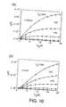
- FIG. 1shows different device configurations of solution processed, all-polymer TFTs
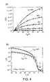
- FIG. 2shows transfer characteristics of polymer TFTs according to FIG. 1 c with a F8T2 active layer, a PVP gate insulating layer, and a PEDOTIPSS gate electrode;
- FIG. 3shows transfer characteristics of polymer TFTs according to FIG. 1 c with a F8T2 active layer, a PVP gate insulating layer, and a PEDOT/PSS gate electrodes deposited with the sample held at room temperature (a) and approximately 50° C. (b).
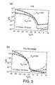
- FIG. 4shows output (a) and transfer characteristics (b) of a F8T2 all-polymer TFT containing a F8 diffusion barrier and a PVP surface modification layer as in FIG. 1( a );
- FIG. 5shows transfer characteristics of F8T2 all-polymer TFTs as in FIG. 1( a ) with a TFB (a) and polystyrene (b) diffusion barrier and a PVP surface modification layer;
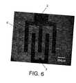
- FIG. 6shows an optical micrograph of an all-polymer TFT according to FIG. 1( a ) with an F8T2 active layer and source-drain electrodes printed directly onto a bare glass substrate;
- FIG. 7shows the fabrication of TFTs with small channel length and small overlap capacitance through patterning of the substrate surface into hydrophobic and hydrophilic areas
- FIG. 9shows optical micrographs taken during the deposition of ink droplets in the vicinity of a polyimide bank.
- FIG. 12shows a schematic diagram (a) Dektak profilometry and optical micrographs (b) of the process of forming via holes by successive deposition of methanol droplets onto a 1.3 ⁇ m thick PVP gate dielectric layer and (c) dependence of the via-hole outer and inner diameter on the diameter of the inkjet droplets and the thickness of the PVP layer;
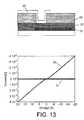
- FIG. 13shows the current-voltage characteristics through a via hole with a bottom PEDOT electrode and a top electrode.
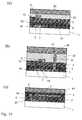
- FIG. 14illustrates different processes to fabricate via-holes
- FIG. 15shows applications of via holes such as logic inverters (depletion-load (a), enhancement-load (b) and resistance-load (c)), and multilevel interconnect schemes (d);
- FIG. 16shows the characteristics of enhancement-load inverter circuits as in FIG. 1( a ) fabricated with printed all-polymer TFrs with different ratios of the sizes WIL of the two transistors.
- FIG. 17shows an alternative bottom-gate device configuration
- FIG. 18shows a schematic drawing of an active matrix pixel in which the display or memory element is controlled by a voltage (a) or a current (b);
- FIG. 19shows possible configurations of the pixel of an active matrix
- FIG. 20shows polarized optical absorption of an aligned F8T2 TFT
- FIG. 21shows (a) polymer TFTs with a patterned active layer island fabricated by printing of semiconducting and dielectric layers and (b) the overlap region between to conducting interconnects separated by a printed insulating island;
- FIG. 22shows a matrix of transistor devices connected by a network of IJP interconnects to fabricate user-defined electronic circuits
- Preferred fabrication methods described hereinpermit the fabrication of an all-organic, solution-processed thin-film transistor, in which none of the layers is converted or cross-linked into an insoluble form.
- Each layer of such a devicemay remain in a form that is soluble in the solvent from which it was deposited. As will be described in more detail below, this enables a simple way of fabricating via-holes through dielectric insulating layers based on local deposition of solvents.
- Such a devicemay, for example, comprise one or more of the following components:
- a diffusion barrier layerthat protects the semiconducting layer and the insulating layer against unintentional doping by impurities and ionic diffusion.
- the fabrication of a first illustrative devicewill now be described with reference to FIG. 1.
- the device of FIG. 1is a thin-film field effect transistor (AFT) configured to have a top-gate structure.
- AFTthin-film field effect transistor
- source-drain electrodes 2 , 3 and interconnect lines between the electrodes and the contact padsare deposited by ink-jet printing a solution of the conducting polymer polyethylenedioxythiophene/polystyrolsulfonate (PEDOT (0.5 weight %)/PSS (0.8 weight %)) in water.
- PEDOTconducting polymer polyethylenedioxythiophene/polystyrolsulfonate
- Other solventssuch as methanol, ethanol, isopropanol or acetone may be added to affect surface tension, viscosity and wetting properties of the ink.
- PEDOTIPSSis obtained commercially from Bayer (available as “Baytron P”).
- the IJP printeris of the piezoelectric type.
- the IJP headis driven with a voltage pulse. Suitable drive conditions to eject droplets of a typical solid content of 0.4 ng per droplet are achieved with a pulse height of 20V, rise time of 10 ⁇ s, and a fall time of 10 ⁇ s. After drying on the glass substrate they produce a PEDOT dot with a typical diameter of 50 ⁇ m, and typical thickness of 500 ⁇ .
- the IJP of the source-drain electrodesis performed in air. Afterwards the samples are transferred to an inert atmosphere glove box system. The substrates are then spun-dried in the organic solvent that will later be used for the deposition of the active semiconducting layer, such as mixed xylenes in the case of polyfluorene polymers. They are then annealed for 20 minutes at 200° C. in inert nitrogen atmosphere to remove residual solvent and other volatile species in the PEDOT/PSS electrodes. Then a 200-1000 ⁇ thick film of the active semiconducting polymer 4 is deposited by spin-coating.
- the active semiconducting layersuch as mixed xylenes in the case of polyfluorene polymers.
- F8T2regioregular poly-3-hexylthiophene
- P3HTregioregular poly-3-hexylthiophene
- F8T2polyfluorene co-polymers
- F8T2is a preferred choice as it exhibits good stability in air during the deposition of the gate electrode in air.
- a 5-10 mg/ml solution of F8T2 in anhydrous, mixed xylenes(purchased from Romil) is spin-coated at 1500-2000 rpm.
- P3HTa 1 weight % solution in mixed xylene was used.
- the underlying PEDOT electrodesare insoluble in a non-polar organic solvent such as xylene.
- a non-polar organic solventsuch as xylene.
- the filmsare then spun-dried in the solvent that will later be used for the deposition of the gate insulator layer 5 , such as isopropanol or methanol.
- a subsequent annealing stepcan then be performed to enhance the charge transport properties of the semiconducting polymer.
- annealingat a temperature above the liquid-crystalline transition results in orientation of the polymer chains parallel to each other.
- annealingis performed at 275-285° C. for 5-20 min under inert N 2 atmosphere.
- the samplesare then rapidly quenched to room temperature to freeze in the orientation of the chains and produce an amorphous glass. If samples are prepared on plain glass substrates without an alignment layer the polymer adopts a multidomain configuration in which several liquid-crystalline domains with random orientation are located within the TFT channel.
- Transistor devices in which the F8T2 is prepared in a glassy state by quenching from a liquid-crystalline phaseexhibit mobilities on the order of 5 ⁇ 10 ⁇ 3 cm 2 Ns, that are by more than an order of magnitude higher than mobilities measured on devices with as-spun F8T2 films. As-deposited devices also exhibit higher turn-on voltages V 0 . This is attributed to a lower density of localized electronic trap states in the glassy phase compared to the as-deposited phase, that is partially crystalline.
- the gate insulating layer 5is deposited by spin-coating a solution of polyhydroxystyreqne (also-called polyvinylphenol (PVP)) from a polar solvent in which the underlying semiconducting polymer is not soluble.
- PVPpolyvinylphenol
- a preferred choice of solventsare alcohols such as methanol, 2-propanol or butanol, in which non-polar polymers such as F8T2 have exceptionally low solubility and do not swell.
- the thickness of the gate insulating layeris between 300 nm (solution concentration 30 mg/ml) and 1.3, ⁇ m (solution concentration 100 mg/ml).
- insulating polymers and solventsthat satisfy the solubility requirements such as poly-vinylalcohol (PVA) in water or poly-methyl-methacrylate (PMMA) in butyl acetate or propylene glycol methyl ether acetate may also be used.
- PVApoly-vinylalcohol
- PMMApoly-methyl-methacrylate
- PMMApoly-methyl-methacrylate
- the gate electrode 6is then deposited over the gate insulating layer.
- the gate electrode layermay be deposited directly over the gate insulating layer (see FIG. 1( c )) or there may be one or more intermediate layers (see FIG. 1( a ) and ( b )), for example for surface modification, diffusion barrier or process reasons such as solvent compatibility.
- a PEDOT/PSS gate 6may be printed directly on top of the PVP insulating layer 5 .
- the substrateis transferred to the IJP station in air again where a PEDOT/PSS gate electrode pattern is printed from a water solution.
- the underlying PVP gate insulating layerhas a low solubility in water such that the integrity of the gate dielectric is preserved during the printing of the PEDOTIPSS gate electrode.
- PVPcontains a large density of polar hydroxyl groups, its solubility in water is low because of the very non-polar polystyrene-like backbone. Similarly PMMA is insoluble in water.
- IJP TFTshows the transfer characteristics of an IJP TFT with a F8T2 semiconducting layer, a PVP gate insulating layer, and IJP PEDOT/PSS source-drain and gate electrodes.
- the device characteristicsare measured under nitrogen atmosphere. Consecutive measurements are shown with increasing (upward triangles) and decreasing (downward triangles) gate voltage, respectively.
- the characteristicsbelong to devices made from a freshly prepared batch (a) and a one-year old batch (b) of PEDOT/PSS (Baytron P).
- Devices with gate electrodes deposited directly onto the PVP layer as in FIG. 1( c )are of the depletion-type. This normally-on behaviour is useful for depletion-type logic circuits such as the simple depletion-load logic inverter (FIG. 14( a )).
- a diffusion barrier layerIn the device of FIG. 1( a ) and ( b ) a thin layer 7 of a non-polar polymer is deposited on top of the PVP gate insulating layer prior to the deposition of the conducting polymer gate electrode. This layer is believed to act as diffusion barrier blocking the diffusion of ionic species through the moderately polar-PVP insulator.
- PVPcontains a high density of polar hydroxyl groups which tend to enhance the conductivity and diffusivity of ions through the film.
- non-polar polymerssuch as poly-9,9′-dioctylfluorene (F8), polystyrene (PS), poly(9,9′-dioctyl-fluorene-co-N-(4-butylphenyl) diphenylamine) (TFB) or F8T2.
- Thin films of these polymers on the order of 50-100 nmcan be deposited on the surface of the PVP gate insulating layer from a solution in a non-polar organic solvent such as xylene, in which PVP is insoluble.
- a surface modification layer 8is deposited on top of the non-polar polymer. This layer provides a hydrophilic rather than hydrophobic surface on to which the PEDOT/PSS may more readily be formed. This permits enables high-resolution printing of the gate electrode pattern.
- a thin layer of PVPcan be deposited from isopropanol solution, in which the underlying diffusion barrier layer is insoluble. The thickness of the PVP layer is preferably less than 50 nm.
- High-resolution printing of PEDOT/PSSis possible on the surface of PVP.
- Alternative surface modification layersmay be used. These include thin layers of soap-like surfactants or polymers containing a hydrophilic and a hydrophobic functional group. These molecules would tend to phase-separate with the hydrophobic and hydrophilic groups being attracted towards the interface with the underlying non-polar polymer and the free surface, respectively.
- Another possibilityis the brief exposure of the surface of the non-polar diffusion barrier to a mild O 2 plasma rendering the surface hydrophilic.
- a suitable plasma treatment that does not degrade the TFT device performanceis exposure to a 13.5 MHz O 2 plasma with a power of 50 W for 12 s.
- a surface modification layer on top of the non-polar diffusion barriermay not be required if the gate electrode is printed from a solvent that is less polar than water such as formulation containing alcohols (isopropanol, methanol etc.).
- the integrity of the layer sequencerelies on the alternating deposition of polymer materials from polar and non-polar solvents. It is desirable that the solubility of a first layer in the solvent used for the deposition of a second layer is less than 0.1% weight per volume, preferably less than 0.01% weight per volume.
- the criterion for solvent compatibilitymay be quantified using the Hildebrand solubility parameters by which the degree of polarity can be quantified (D. W. van Krevelen, Properties of polymers, Elsevier, Amsterdam (1990)).
- Dthe interaction parameter
- Dis smaller than approximately 5 the polymer is soluble in the solvent. If D is between 5-10, swelling is often observed. If D is larger than 10, the polymer is substantially insoluble in the solvent, and no swelling occurs.
- the respective D values for each of the polymer layers and the solvent of the next layershould be larger than approximately 10. This is particularly important for the semiconducting polymer layer and the solvent of the gate dielectric. In the case of F8T2 and isopropanol (butyl acetate) we estimate D to be approximately 16 (12).
- the entire multilayer structuremay be built up by an alternating sequence of polymers that contain mainly polar groups and are soluble in a highly polar solvent such as water, and polymers that contain only a few or do not contain any polar groups and are soluble in a non-polar solvent, such as xylene.
- the interaction parameter Dis large because of the differences of ⁇ p for the polymer layer and solvent of the next layer.
- An example would be a transistor devicecomprising a highly polar source-drain electrode of PEDOT/PSS, a non-polar semiconducting layer such as F8T2, a highly-polar gate dielectric layer such as a polyvinylalcohol deposited from water solution, a non-polar diffusion barrier layer of TFB that also acts as a buffer layer to allow the deposition of the layer sequence, and a PEDOT/PSS gate electrode.
- a transistor devicecomprising a highly polar source-drain electrode of PEDOT/PSS, a non-polar semiconducting layer such as F8T2, a highly-polar gate dielectric layer such as a polyvinylalcohol deposited from water solution, a non-polar diffusion barrier layer of TFB that also acts as a buffer layer to allow the deposition of the layer sequence, and a PEDOT/PSS gate electrode.
- a moderately polar polymeris a polymer that contains both polar and non-polar groups, and is substantially insoluble in a highly polar solvent.
- a moderately polar solventcontains both polar and non-polar groups, but does not substantially dissolve a non-polar polymer.
- a moderately polar solventmay be defined as one where the solubility parameter ⁇ h is largely different from that of the underlying polymer. In this case swelling may be avoided (large D) even if the polar solubility parameter ⁇ p ( ⁇ v ) of the solvent may be similar to that of the underlying polymer layer.
- the moderately polar polymermay contain a specific functional group such as a hydroxyl group that makes it soluble in a solvent containing a functional group that is attracted to the functional group of the polymer. This attraction may be a hydrogen bonding interaction. This functionality of the polymer may be used to enhance its solubility in a moderately polar solvent and decrease its solubility in a polar solvent.
- An example of a moderately polar polymeris a PVP gate dielectric layer sandwiched between a non-polar semiconductor layer and a PEDOT/PSS gate electrode layer (FIG. 1 c ).
- the deviceexhibits clean, near-ideal normally-off transistor action with turn-on at V 0 ⁇ 0V.
- the threshold voltage shift between upward (upward triangles) and downward (downward triangles) voltage sweepsis ⁇ 1V.
- the device characteristicsare very similar to those of standard devices fabricated under inert atmosphere conditions with Au source-drain and gate electrodes.
- Normally-off devices containing a diffusion barrierare preferred compared to the depletion-type device described above, since it is expected that the former exhibit better long term threshold voltage stability and better lifetime due to suppression of ionic diffusion.
- any solution processible conjugated polymeric or oligomeric material that exhibits adequate field-effect mobilities exceeding 10 ⁇ 3 cm 2 Ns, preferably exceeding 10 ⁇ 2 cm 2 Ns,may be used. Suitable materials are reviewed for example in H. E. Katz, J. Mater. Chem. 7, 369 (1997), or Z. Bao, Advanced Materials 12, 227 (2000).
- Printed TFTshave been fabricated with a range of semiconducting polymers as the active semiconducting layer, such as F8T2 (see above), or regioregular P3HT deposited from mixed xylene solution.
- F8T2see above
- regioregular P3HTdeposited from mixed xylene solution.
- the field-effect mobility of 0.05-0.1 cm 2 Nsis somewhat higher than in the case of F8T2.
- regioregular P3HTis unstable against doping by oxygen and/or water, resulting in an increase of the film conductivity during the printing steps in air and poor ON-OFF current ratio. This is related to the relatively low ionisation potential of P3HT, I p 4.9 eV. High ON-OFF current ratios of >10 6 have been demonstrated for P3HT, but this requires a reductive dedoping step after the deposition, such as exposure to hydrazine vapour (H. Sirringhaus, et al., Advances in Solid State Physics 39, 101 (1999)).
- a preferred class of materials to achieve good environmental stability and high mobilityare A-B rigid-rod block-copolymers containing a regular ordered sequence of A and B blocks.
- Suitable A blocksare structurally well defined, ladder type moieties with a high band gap, that have high ionisation potentials larger than 5.5 eV as a homopolymer and good environmental stability.
- suitable A blocksare fluorene derivatives (U.S. Pat. No. 5,777,070), indenofluorene derivatives (S. Setavesh, Macromolecules 33, 2016 (2000)), phenylene or ladder-type phenylene derivatives (J. Grimme et al., Adv. Mat. 7, 292 (1995)).
- Suitable B blocksare hole-transporting moieties with lower bandgaps that contain heteroatoms such as sulphur or nitrogen, and as a homopolymer have ionisation potentials less than 5.5 eV.
- Examples of hole-transporting B blocksare thiophene derivatives, or triarylamine derivatives.
- the effect of the B blockis to lower the ionisation potential of the block copolymer.
- the ionisation potential of the block copolymeris preferably in the range of 4.9 eV ⁇ Ip 5.5 eV. Examples of such copolymers are F8T2 (ionisation potential 5.5 eV) or TFB (U.S. Pat. No. 5,777,070).
- Suitable hole transporting polymersare homopolymers of polythiophene derivatives with ionisation potential larger than 5 eV, such as polythiophenes with alkoxy or fluorinated side chains (R. D. McCullough, Advanced Materials 10, 93 (1998)).
- soluble electron transporting materialsmay be used as well. These require a high electron affinity larger than 3 eV, preferably larger than 3.5 eV, to prevent residual atmospheric impurities such as oxygen to act as carrier traps. Suitable materials may include solution processible electron-transporting small molecule semiconductors (H. E. Katz et al., Nature 404, 478 (2000)), or polythiophene derivatives with electron-deficient fluorinated side chains.
- AB-type block copolymers with a structurally-well defined, ladder-type A block with a high ionisation potential larger than 5.5 eV and an electron-transporting B block that increases the electron affinity of the copolymer to a value higher than 3 eV, preferably higher than 3.5 eVare also suitable.
- a blocksare fluorene derivatives (U.S. Pat. No. 5,777,070), indenofluorene derivatives (S. Setayesh, Macromolecules 33, 2016 (2000)), phenylene or ladder-type phenylene derivatives (J. Grimme et al., Adv. Mat. 7, 292 (1995)).
- electron-transporting B blocksexamples include benzothiadiazole derivatives (U.S. Pat. No. 0.5,777,070), perylene derivatives, naphtalenetetracarboxylic diimide derivatives (H. E. Katz et al., Nature 404, 478 (2000)) or fluorinated thiophene derivatives.
- the channel length L of the transistors and the overlap between source/drain and gate dhave to be as small as possible, that is typically a few microns.
- the most critical dimensionis L, because the operation speed of a transistor circuit is approximately proportional to L ⁇ 2 . This is particularly important for semiconducting layers with relatively low mobility.
- This confinement techniquecan be used to permit fine-resolution deposition of a deposited material on to a substrate.
- the surface of the substrateis first treated in order to render selected parts of it relatively attractive and relatively repellent for the material to be deposited.
- the substratecould be pre-patterned so as to be partially hydrophobic in some areas and partially hydrophilic in other areas. With the pre-patterning step performed at high resolution and/or precise registration the subsequent deposition can be accurately defined.
- FIG. 7illustrates the formation of a device of the type shown in FIG. 1( c ) but with an especially fine channel length L. Like parts are numbered as for FIG. 1( c ).
- FIG. 7( a )illustrates a method to fabricate a pre-patterned substrate.
- FIG. 7( b )illustrates printing and ink confinement on a pre-patterned substrate.
- a thin polyimide layer 10is formed over the glass sheet 1 .
- This polyimide layeris finely patterned to remove it in the places in which the source-drain electrodes are to be formed.
- the removal stepmay be done by a photolithographic process to allow fine feature definition and/or accurate registration.
- the polyimidemay be covered with a layer of photoresist 11 .
- the photoresistcan be patterned photolithographically to remove it in the places where the polyimide is to be removed.
- the polyimideis removed by a process to which the photoresist is resistant. Then the photoresist can be removed to leave the accurately patterned polyimide.
- Polyimideis selected because it is relatively hydrophobic, whereas the glass substrate is relatively hydrophilic.
- PEDOT material to form the source-drain electrodesis deposited by ink-jet printing onto the hydrophilic substrate areas 12 .
- ink droplets spreading on the glass substrate areashit the boundary of a hydrophobic polyimide region 10 the ink is repelled and prevented from flowing into the hydrophobic surface areas.
- the inkis deposited in the hydrophilic surface areas only and high-resolution patterns with small gaps and transistor channel lengths of less than 10 ⁇ m can be defined (FIG. 7( b )).
- FIG. 7( a )One example of a process by which the polyimide may be removed, or which may be employed to enhance the relative surface effects after removal of polyimide, is illustrated in FIG. 7( a ).
- the polyimide layer 10 and the photoresist 11are exposed to an oxygen plasma.
- the oxygen plasmaetches the thin (500 ⁇ ) polyimide layer faster than the thick (1.5 ⁇ m) photoresist layer.
- the exposed bare glass surface 12 in the area of the source-drain electrodesis made very hydrophilic by exposure to an O 2 plasma prior to removal of the photoresist. Note that during the removal of polyimide the surface of the polyimide is protected by the photoresist and remains hydrophobic.
- the polyimide surfacecan be made even more hydrophobic by an additional exposure to a CF 4 plasma.
- CF 4 plasmafluorinates the polyimide surface, but does not interact with the hydrophilic glass substrate. This additional plasma treatment may be performed prior to removal of the photoresist, in which case only the side walls of the polyimide pattern 10 become fluorinated, or after removal of the resist.
- the contact angle of PEDOT/PSS in water on O 2 plasma-treated 7059 glassis ⁇ glass ⁇ 20° compared to a contact angle of ⁇ PI ⁇ 70°-80° on the polyimide surface.
- the contact angle of PEDOT/PSS in water on fluorinated polyimideis 120°.
- PEDOTIPSSWhen PEDOTIPSS is deposited from a water solution onto the pre-patterned polyimide layer as described, the PEDOT/PSS ink is confined to the source-drain electrode areas even if the channel length L is only a few microns (FIG. 7( b )).
- deposition of the ink droplets 13is onto the hydrophilic substrate areas 12 at a distance d between the centre of the droplet and the polyimide boundary.
- dneeds to be sufficiently small that the boundary is reached by the spreading ink and the PEDOT film extends all the way to the polyimide boundary.
- dneeds to be sufficiently large that the rapidly spreading ink does not “spill over” into the hydrophobic surface areas. This would increase the risk of PEDOT deposition on top of the polyimide region 10 defining the TFT channel and may give rise to short circuits between source and drain electrodes.
- d ⁇ 30-40 ⁇ mwas found suitable for PEDOT droplets with a solid content of 0.4 ng deposited with a lateral pitch of 12.5 ⁇ m between two successive droplets onto O 2 plasma treated 7059 glass a value of d ⁇ 30-40 ⁇ m was found suitable.
- the optimum value ddepends on the wetting properties on the surface as well as on the deposition pitch, that is the lateral distance between subsequently deposited droplets, the frequency, with which droplets are deposited, and the drying time of the solution.
- the hydrophobic confinement layer to define the channel length of the transistormay also provide a second functionality. It may be used as an aligning template for the subsequent deposition of the semiconducting polymer in the channel of the transistor.
- the polyimide layer 10may be mechanically rubbed or photoaligned and can then be used as an alignment layer 9 (FIG. 1( b )) to provide monodomain alignment of a liquid-crystalline semiconducting polymers 4 .
- the gate electrode 6may be similarly confined by a patterned layer 14 formed on top of the gate insulating layer 5 that provides attractive and repelling surface areas for the solution from which the gate electrode is deposited.
- the patterned layer 6may be aligned with respect to the source-drain pattern to minimize the overlap area between sourceldrain and gate electrodes (FIG. 7( c ).
- Materials other than polyimidemay be used for the pre-patterned layer.
- Other accurate pre-patterning techniques than photolithographymay be used.
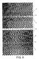
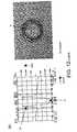
- FIG. 8demonstrates the ability of a structure of relatively hydrophobic and hydrophilic layers to confine liquid “ink” deposited by ink-jet printing.
- FIG. 8shows optical micrographs of substrates including thin strips of polyimide 10 that have been treated as described above to be relatively hydrophobic and larger regions of the bare glass substrate 12 that have been treated as described above to be relatively hydrophilic.
- PEDOT material for the source and drain electrodeshas been deposited by ink-jet printing of a series of droplets running in lines 2 and 3 close to the strips 10 .
- FIG. 9shows photographs of the ink jet deposition process in the vicinity of a polyimide strip 10 .
- the imageswere taken with a stroboscopic camera mounted underneath the transparent substrate.
- the edges of the polyimide pattern 10can be seen as white lines.
- the ink droplets 21are ejected from the nozzle of the ink jet head 20 and land with their centre being a distance d away from the polyimide strip 10 . Images such as this can be used for precise local alignment of the ink-jet deposition with respect to the strip pattern 10 , and may also used to automate the local alignment procedure using pattern recognition (see below).
- FIGS. 10 and 11show output and transfer characteristics of transistors formed as in FIG. 7( c ) and having channel lengths L of 20 ⁇ m and 7 ⁇ m respectively, defined by means of the differential wetting process described above. In both cases the channel width W is 3 mm.
- FIG. 10( a )shows output characteristics of the 20 ⁇ m device.
- FIG. 10( b )shows output characteristics of the 7 ⁇ m device.
- FIG. 11( a )shows transfer characteristics of the 20 ⁇ m device.
- FIG. 11( b )shows transfer characteristics of the 7 ⁇ m device.
- the 7 ⁇ m deviceshows characteristic short channel behaviour with reduced current at small source-drain voltage and finite output conductance in the saturation regime.
- Ink confinementis a result of the difference in wetting properties on the hydrophobic and hydrophilic surfaces, and does not require the existence of a topographic profile.
- the polyimide filmcan be made very thin (500 ⁇ ), that is much thinner than the size of the inkjet droplets in the liquid state (several micrometers). Therefore, alternative techniques to fabricate a substrate pre-pattern can be used, such as the functionalization of the surface of the glass substrate with a patterned self-assembled monolayer (SAM), for example a SAM containing hydrophobic alkyl or fluorogroups such as trifluoropropyl-trimethoxysilane or polar groups such as alkoxy groups.
- SAMself-assembled monolayer
- the SAMcan be patterned by suitable techniques such as UV light exposure through a shadow mask (H. Sugimura et al., Langmuir 2000, 885 (2000)) or microcontact printing (Brittain et al., Physics World May 1998, p. 31).
- Pre-patterning of the substrateis readily compatible with the process flow described above as the pre-patterning is performed prior to the deposition of the layers of the TFT. Therefore, a broad range of patterning and printing techniques can be used to generate the high-resolution pre-pattern without risking degradation of the active polymer layers.
- Similar techniquescan be applied to pre-pattern the surface of the gate insulating layer or the surface modification layer prior to the deposition of the gate electrode to achieve small overlap capacitance.
- the gate electrode 6may be confined by a patterned layer 14 .
- One possible embodiment of such pre-patterningis microcontact printing or UV photopatterning of a self-assembled monolayer (SAM) containing chlorosilane or methoxy silane groups, such as octadecyltrichlorosilane. These molecules form stable monolayers on the surface of a SiO 2 or glass substrate where they chemically bond to the hydroxyl groups on the polar surface, and render the surface hydrophobic.
- SAMself-assembled monolayer
- a surface free energy pattern consisting of a fine hydrophilic line with a well-defined small overlap with the source-drain electrodes surrounded by SAM-coated, hydrophobic regionscan easily be defined by soft lithographic stamping.
- the stampingmay be performed under an optical microscope or a mask aligner in order to align the stamp pattern with respect to the underlying source-drain electrodes.
- a conducting, water-based polymer inkis deposited on top the deposition is confined to the fine, hydrophilic line defined by the self-assembled monolayer. In this way a smaller linewidth can be achieved than the normal linewidth on an unpatterned gate dielectric layer. This results in a reduction of sourceldrain-to-gate overlap capacitance.
- a quantity of a suitable solvent 29is deposited locally on top of the layers through which the via hole is to be formed.
- the solventis selected so that it is capable of dissolving the underlying layers through which the hole is to be formed.
- the solventsinks through the layers by progressive dissolution until the via hole is formed.
- the dissolved materialis deposited onto the side walls W of the via-hole.
- the type of solvent and the method of depositing itmay be selected for individual applications. However, three preferred aspects are:
- the solventis deposited by a selective process such as IJP, whereby accurately controlled volumes of the solvent may be applied accurately to the desired location on the substrate;
- FIG. 12( a )illustrates the deposition of a droplet 29 of methanol solvent (containing 20 ng per droplet) on a partially formed transistor device of the general type illustrated in FIG. 1( c ).
- the partial device of FIG. 12( a )includes a 1.3 ⁇ m thick PVP insulating layer 28 , an F8T2 semiconducting layer 27 , a PEDOT electrode layer 26 and a glass substrate 25 .
- Methanolis selected as the solvent because of its ability to readily dissolve PVP; because it can easily evaporate so as not to hinder subsequent processing; and because it has satisfactory wetting properties for PVP.
- an IJP printing headis moved to the location on the substrate at which the via hole is desired to be formed. Then the necessary number of suitably-sized droplets of methanol are dropped from the IJP head until the via is complete. The period between successive drops is selected for compatibility with the rate at which the methanol dissolves the layers of the device. It is preferred that each drop has fully or almost fully evaporated before the next drop is deposited. Note that when the via-hole reaches the bottom non-polar semiconducting layer the etching stops such that underlying layers are not removed. Other solvents such as isopropanol, ethanol, butanol or actone may also be used.
- FIG. 12( b )illustrates the effect of the dropping of several droplets of methanol in sequence onto the via hole location.
- the right panelsshow micrographs of the device after 1, 3 and 10 droplets have been dropped.
- the left panelsshow Dektak surface profile measurements of the same devices across the via hole as it is formed. (The location of the via hole is indicated generally at position “V” in each panel).
- a crateropens up in the PVP film.
- the depth of the craterincreases as successive droplets act, and after approximately 6 droplets the surface of the underlying F8T2 layer is uncovered.
- the dissolved PVP materialis deposited in a wall W at the sides of the via-hole.
- the diameter of the via-holeis on the order 50 ⁇ m limited by the size of the droplet. This size is suitable for many applications such as logic circuits, and large area displays.
- the via-hole diameteris determined by the size of the inkjet solvent droplets.
- the diameter of the holewas observed to be directly proportional to the diameter of the droplets (see FIG. 12 c ).
- the outer diameter of the side wallis determined by the size and spreading of the first droplet, and is independent of the thickness of the polymer layer that is dissolved.
- the inner diameter of the side walldecreases with increasing polymer thickness. For applications where even smaller holes are required, such as in high-resolution displays, even smaller droplet sizes can be used, or the substrate surface can be pre-patterned by a suitable technique to confine the droplet on the surface as described above. Other solvents may also be used.
- the mechanism for via-hole formationi.e. the movement of material to the side walls, is believed to be similar to that of the well-known coffee-stain effect, which occurs if the contact line of a drying droplet containing a solute is pinned. Pinning can occur for example due to surface roughness or chemical heterogeneity. Note that deposition of a good solvent always generates surface roughness during dissolution. When the solvent evaporates, capillary flow occurs in order to replace the solvent evaporating near the contact line. More solvent is evaporating near the contact line because of the larger surface-to-bulk ratio near the contact line.
- the capillary flow velocityis large compared to the typical diffusion velocity, such that solute is carried to the edges of the droplet, and solute deposition occurs only near the rim, but not in the centre of the drying droplet (R. D. Deegan et al., Nature 389, 827 (1997)). Diffusion of solute would tend to favour homogeneous redeposition of the polymer over the whole area upon drying of the solvent, rather than formation of a side wall.
- the surface of the substratemay be treated, for example with a self-assembled monolayer with a larger repellence for the solvent.
- the self-assembled monolayermay be patterned, such as to provide hydrophobic and hydrophilic surface regions, in order to confine the deposition of the solvent to a small area.
- the depth and etch rate of the via holecan be controlled by a combination of the number of drops of solvent that are dropped, the frequency at which they are deposited, and the rate of evaporation of the solvent in comparison to the rate at which it is capable of dissolving the substrate.
- the environment in which the deposition takes place and the substrate temperaturemay influence the evaporation rate.
- a layer of material that is insoluble or only slowly soluble to the solventmay be used to limit the depth of dissolution.
- the layer sequence of the TFTconsists of alternating polar and non-polar layers, it is possible to choose solvents and solvent combinations such that etching stops at well defined depths.
- FIG. 13( a )shows a device of the type shown in FIG. 12( a ) but including a gold electrode 25 formed after the making of a via hole as described above.
- FIG. 13shows at curve 30 the current voltage characteristics measured between the bottom PEDOT electrode 25 and a conducting electrode 29 deposited on top of the PVP gate insulating layer 28 .
- the diameter of the via holewas 50 ⁇ m.
- curve 31shows a reference sample, in which no via-holes are located in the overlap region between the top and bottom electrodes. The characteristics clearly show that the current through the via-hole is several orders of magnitude higher than the leakage current through the gate insulator in the absence of the via hole.
- the measured current through the via holeis limited by the conductivity of the PEDOT electrodes, as can be seen by performing conductivity measurements of the individual PEDOT electrodes. It is not limited by the resistance of the via-hole, such that only a lower limit estimate for the via-hole resistance R v can be obtained from these measurements: R v ⁇ 500 k ⁇ .
- FIG. 14( a )shows a device in which a via hole has been formed and the gate electrode then deposited without an intervening diffusion barrier layer.
- FIG. 14( b )shows a similar device in which after formation of the via hole a diffusion barrier polymer 7 has been formed before deposition of the gate electrode 6 .
- the diffusion barrier layerneeds to exhibit good charge transporting properties in order to minimise the via-hole resistance R v .
- a suitable diffusion barrieris a thin layer of TFB as shown in FIG. 5( a ).
- the semiconductor layersmay also be removed at the via hole site. This is preferably done after the diffusion barrier has been formed.
- the diffusion barrier 7 and the semiconducting polymer 4can be locally dissolved by IJP deposition of a good solvent for them—such as xylene in this example. By mixing good solvents for both the semiconducting and the insulating material, both layers may be dissolved at the same time. A device in which this has been done followed by deposition of the gate electrode is shown in FIG. 14( c ).
- Mixtures of solventscan also be used to reduce the diameter of the via-hole by increasing the contact angle of the solvent mixture on the layer to be dissolved.
- An alternative technique to forming a via hole interconnection and then depositing a conductive material to bridge itis to locally deposit a material that is capable of locally modifying the underlying layer(s) substrate so as to render them conductive.
- a material that is capable of locally modifying the underlying layer(s) substrateso as to render them conductive.
- One exampleis the local IJP deposition of a solution containing a mobile dopant that is able to diffuse into one or several of the layers. This is illustrated in FIG. 14( d ), where region 32 indicates material that has been rendered conductive by treatment with a dopant.
- the dopantmay be a small conjugated molecule such as a triarylamine like N,N′-diphenyl-N,N′-bis(3-methylphenyl)(1,1′-biphenyl)-4,4′-diamine (TPD).
- TPDN,N′-diphenyl-N,N′-bis(3-methylphenyl)(1,1′-biphenyl)-4,4′-diamine
- TPDN,N′-diphenyl-N,N′-bis(3-methylphenyl)(1,1′-biphenyl)-4,4′-diamine
- FIG. 16shows plots of the characteristics of enhancement-load inverter devices formed with two normally-off transistor devices as in FIG. 15( b ). Two inverters with different ratio of the channel width to channel length ratio (W/L) for the two transistors are shown (plot 35 ratio 3:1, plot 36 ratio 5:1)).
- the output voltagechanges from a logic high ( ⁇ 20V) to a logic low ( ⁇ 0V) state when the input voltage changes from logic low to logic high.
- the gain of the inverterthat is the maximum slope of the characteristics is larger than 1, which is a necessary condition to allow the fabrication of more complex circuits such as ring oscillators.
- Via-holes as described abovemay also be used to provide electrical connections between interconnect lines in different layers. For complex electronic circuits multilevel interconnect schemes are required. This may be fabricated by depositing a sequence of interconnects 72 and different dielectric layers 70 , 71 deposited from compatible solvents (FIG. 15( d )). Via-holes 73 can then be formed in the way described above with the interconnect lines providing automatic etch stop. Examples for suitable dielectric materials are polar polymers ( 70 ) such as PVP and non-polar dielectric polymers ( 71 ) such as polystyrene. These can be deposited alternatively from polar and non-polar solvents. Via-holes can be opened by local deposition of good solvents for the respective dielectric layer while the underlying dielectric layer is providing an etch-stopping layer.
- FIG. 17Other device configurations than the top-gate configuration shown in FIG. 1 may be used.
- An alternative configurationis the more standard bottom-gate configuration shown in FIG. 17, in which it is also possible to incorporate a diffusion barrier 7 and surface modification layer 8 if required.
- FIG. 17like parts are numbered as for FIG. 1.
- Other device configurations with different layer sequencesmay also be used.
- Devices other than transistorsmay be formed in an analogous way.
- PEDOT/PSSmay be replaced by any conducting polymer that can be deposited from solution. Examples include polyaniline or polypyrrole.
- PPSpolymeric dopant
- bgood thermal stability and stability in air
- ca work function of ⁇ 5.1 eV that is well matched to the ionisation potential of common hole-transporting semiconducting polymers allowing for efficient hole charge carrier injection.
- Efficient charge carrier injectionis crucial in particular for short-channel transistor devices with channel lengths L ⁇ 10 ⁇ m.
- source-drain contact resistance effectsmay limit the TFT current for small source-drain voltages (FIG. 10( b )).
- injection from PEDOT source/drain electrodesis more efficient than injection from inorganic gold electrodes. This indicates that a polymeric source-drain electrode with an ionisation potential that is well matched to that of the semiconductor may be preferable to an inorganic electrode material.
- the conductivity of PEDOT/PSS deposited from a water solutionis on the order of 0.1-1 S/cm. Higher conductivities up to 100 S/cm can be obtained with formulations that contain a mixture of solvents (Bayer CPP 105T, containing isopropanol and N-methyl-2-pyrrolidone (NMP)). In the latter case care needs to be taken that the solvent combination of the formulation is compatible with the solubility requirements of the layer sequence.
- NMPN-methyl-2-pyrrolidone
- the processes and devices described hereinare not limited to devices fabricated with solution-processed polymers.
- Some of the conducting electrodes of the TFT and/or the interconnects in a circuit or display devicemay be formed from inorganic conductors, that can, for example, be deposited by printing of a colloidal suspension or by electroplating onto a pre-patterned substrate.
- inorganic conductorsthat can, for example, be deposited by printing of a colloidal suspension or by electroplating onto a pre-patterned substrate.
- PEDOT/PSS portions of the devicemay be replaced with an insoluble conductive
- materialsuch as a vacuum-eposited conductor.
- the semiconducting layermay also be replaced by another solution-processible semiconducting material.
- Possibilitiesinclude small conjugated molecules with solubilising side chains (J. G. Laquindanum, et al., J. Am. Chem. Soc. 120, 664 (1998)), semiconducting organic-inorganic hybrid materials self-assembled from solution (C. R. Kagan, et al., Science 286, 946 (1999)), or solution-deposited inorganic semiconductors such as CdSe nanoparticles (B. A. Ridley, et al., Science 286, 746 (1999)).
- the electrodesmay be patterned by techniques other than ink-jet printing. Suitable techniques include soft lithographic printing (J. A. Rogers et al., Appl. Phys. Lett. 75, 1010 (1999); S. Brittain et al., Physics World May 1998, p. 31), screen printing (Z. Bao, et al., Chem. Mat. 9, 12999 (1997)), photolithographic patterning (see WO 99/10939) or plating, or simple dip-coating of a patterned substrate with hydrophobic and hydrophilic surface regions. Ink-jet printing is considered to be particularly suitable for large area patterning with good registration, in particular for flexible plastic substrates.
- the device(s)could be deposited on to another substrate material, such as Perspex or a flexible, plastic substrate such as polyethersulphone.
- a substrate materialsuch as Perspex or a flexible, plastic substrate such as polyethersulphone.
- a materialis preferably in the form of a sheet, is preferably of a polymer material, and may be transparent and/or flexible.
- one or more componentssuch as a semiconducting layer may also be deposited by vacuum deposition techniques and/or patterned by a photolithographic process.
- Devices such as TFTs fabricated as described abovemay be part of a more complex circuit or device in which one or more such devices can be integrated with each other and or with other devices.
- Examples of applicationsinclude logic circuits and active matrix circuitry for a display or a memory device, or a user-defined gate array circuit.
- the basic component of a logic circuitis the inverter shown in FIG. 15. If all transistors on the substrate are either of the depletion or of the accumulation type three possible configurations are possible.
- the depletion-load inverter(FIG. 15( a )) is suitable for device that are normally on, (FIG. 1( c ) and 3 ), and the enhancement-load configuration (FIG. 15( b )) is used for normally-off transistors (FIGS. 1 ( a/b ) and 4 ). Both configurations require a via-hole between the gate electrode of the load transistor and its source and drain electrode, respectively.
- An alternative configurationis the resistance load inverter (FIG. 15( c )).
- the latter devicecan be fabricated by printing a thin, narrow PEDOT line of adequate length and conductivity as the load resistor.
- PEDOTconductivity of PEDOT
- the conductivity of Baytron P PEDOT/PSS with a PEDOT/(PEDOT+PSS) weight ratio of 0.4was measured to be on the order of 0.2 S/cm for an as-deposited film.
- annealing to 280° C. for 20 min under N 2 atmospherethe conductivity increased to 2 S/cm.
- diluting the solution with PSSthe conductivity could be decreased by orders of magnitude.
- a conductivity of 10 ⁇ 3 S/cmwas measured after annealing at 280° C.
- Resistors with a resistance of 50 M ⁇were fabricated by inkjet printing a line of PEDOT with a width on the order of 60 ⁇ m and a length of 500 ⁇ m.
- the different inkjet printing components that have been developedi.e. transistors, via-hole interconnections, resistors, capacitors, multilayer interconnect schemes etc., can be integrated to fabricate integrated electronic circuits by a combination of direct printing and solution processing, Inkjet printing can be used for all processing steps where lateral patterning is required.
- the simple inverter circuits described aboveare the building blocks for more complex logic circuits.
- Solution-processed TFTs as described abovemay be used as pixel switching transistors of active matrix displays such as liquid-rystal (LCD) or electrophoretic displays (B. Comiskey et al., Nature 394, 253 (1998)) for which a suitable circuit is shown in FIG. 18( a ); and light-emitting diode displays (H. Sirringhaus, et al., Science 280, 1741 (1998), for which a suitable circuit is shown in FIG. 18( b ); or as an active matrix addressing element of a memory device, such as a random access memory (RAM).
- FIGS. 18 ( a ) and ( b )transistors T 1 and/or T 2 may be formed from transistors as described above.
- Features 40represent a display or memory element with current and voltage supply pads.
- FIG. 19Examples of possible device configurations to control the voltage on the electrode of a LCD or an electrophoretic display are shown in FIG. 19, in which like parts are numbered as for FIG. 1.
- the gate insulating layermay include a multilayer structure containing a diffusion barrier and/or surface modification layer, as in FIG. 1( a ).
- the source and gate electrodes 2 , 3 of the TFTare connected to the data 44 and addressing 43 lines of the active matrix, which may be fabricated from a different conducting material to achieve adequate conductivity over longer lengths.
- the drain electrode 3 of the TFTmay also be the pixel electrode 41 .
- the pixel electrodemay be formed from a different conducting material as in FIG. 19. In devices which rely on application of an electric field rather than charge carrier injection it is not required that this electrode 41 is in direct contact display element 40 , such as a liquid crystal or electrophoretic ink etc. In this configuration the total pixel area occupied by the TFT and interconnect lines has to be kept small to achieve adequate aperture ratio and to reduce potential cross-talk between the display element 40 and the signals on the data and addressing lines 43 and 44 .
- FIG. 19( b )The configuration in FIG. 19( b ) is more complicated. However, the whole pixel or a large portion of the pixel area is available for the TFTs and interconnect lines, and the display element is shielded from the signals on the data and addressing lines 44 , and 43 by the pixel electrode 41 . Fabrication of this configuration requires an additional dielectric layer 42 and a via-hole filled with conductive material 45 to connect the pixel electrode 41 to the TFT drain electrode 3 . The via-hole can be fabricated by the procedure described above.
- FIG. 20shows optical absorption spectra measured on a F8T2 polymer TFT, in which the polymer chains are aligned uniaxially by depositing the liquid-crystalline semiconducting polymer on a rubbed polyimide alignment layer which also serves as the pre-patterning layer for high-resolution printing. It can be seen that the device is highly transparent in most of the visible spectral range because of the relatively high band gap of F8T2.
- Another advantage of the low optical absorption of the semiconducting layeris the reduced photosensitivity of the TFT characteristics to visible light.
- a black matrixhas to be used to prevent large OFF current under light illumination.
- polymer TFTs with wide band gap semiconductorsit is not required to protect the TFTs from ambient light and from the backlight of the display.
- FIG. 19( b )The configuration in FIG. 19( b ) is also well suited for the drive transistor TI of an LED display (FIG. 18( b )), since it allows the drive current of the TFT to be increased by fabrication of an interdigitated array of source-drain electrode with large channel width W making use of the full area underneath the pixel electrode 41 .
- the bottom-gate TFT configuration of FIG. 17can also be used in all of the above applications (FIG. 19( c )).
- PEDOT/PSS TFTthe contact between the PEDOT/PSS TFT and pixel electrodes 2 , 3 , 6 and the metallic interconnect lines 43 , 44 , and 41 .
- PEDOT/PSSDue to its strong acidic nature PEDOT/PSS is not compatible with many common inorganic metals such as aluminium. Aluminium is easily oxidised in contact with PEDOT/PSS.
- One possible solutionis the fabrication of interconnect lines and pixel electrodes 43 , 44 , and 41 from indium-tin-oxide (ITO) or tantalum, tungsten and other refractory metals or another material having more stability in this environment, or the use of a suitable barrier layer.
- ITOindium-tin-oxide
- tantalumtungsten and other refractory metals or another material having more stability in this environment, or the use of a suitable barrier layer.
- TFTswith a small channel length by printing onto a pre-patterned substrate indicated as 10 in FIG. 19, as described above.
- Similar device configurations for active matrix transistor switchescan also be used if the pixel element to be controlled is not a display element but a memory element such as a capacitor or a diode, as for example in a dynamic random access memory.
- FIG. 21( a )shows a device in which an active layer island of the semiconducting layer 4 and the gate insulating layer 5 may be printed directly. In this case no via-holes are required, but connections can be made by direct printing of a suitable gate electrode pattern 6 . In areas where addressing or interconnect lines 43 , 44 overlap thick islands of a dielectric polymer 46 may be printed to provide electrical insulation (FIG. 21( b )).
- a plurality of devices formed as described abovemay be formed on a single substrate and interconnected by conductive layers.
- the devicesmay be formed on a single level or on more than one level, some devices being formed on top of others.
- the technology developed here for the fabrication of ink-jet printed transistors, via-holes and interconnect linesmay be used to fabricate integrated electronic circuits by ink-jet printing.
- a prefabricated substrate containing an array of hydrophilic and hydrophobic surface regionsmay be used that define the channel length of the transistors and/or the width of the interconnect lines.
- the substratemay also contain an array of highly conducting metallic interconnect lines.
- An integrated circuitis then fabricated by forming electrical connections between pairs of transistors and suitable interconnects using ink-jet printing of via-holes and conducting lines.
- the prefabricated substratemay already contain one or more of the components of the transistor devices.
- the substratemay contain, for example, an array of completed inorganic transistor devices each having at least one exposed electrode.
- ink-jet fabrication of an integrated circuitwould comprise the formation of electrical connections between pairs of transistors and the deposition of a single or multilevel interconnect scheme using ink-jet printed via-holes, interconnect lines, and isolation pads (see FIG. 15( d )).
- the electronic circuitmay also comprise other active and passive circuit elements such as display or memory elements or capacitive or resistive elements.
- a unit having a plurality of transistorsmay be formed and then configured for a specific subsequent use by means of solution-based processing.
- a substrate having a plurality of transistors 50 of the type shown in FIG. 1( a ), (b) or (c), in the form of a gate array, for example,may be formed on a plastic sheet (FIG. 22).
- Other devicessuch as diodes or capacitors may also be formed on the sheet.
- the sheetmay be placed in an ink-jet printer having a printing head for a suitable solvent for forming yia-holes 52 (e.g. methanol) and a suitable material for forming conductive tracks 53 and for filling via-holes (e.g. PEDOT).
- the ink-jet printermay be operable under the control of a suitable programmed computer, having knowledge of the location and configuration of the transistors on the sheet. Then, by a combination of via-hole formation and interconnection steps the ink-jet printer can configure the circuit for performing a desired electronic or logic function, by interconnecting the transistors in the desired way.
- This technologythus allows for the formation of logic-specific circuits on substrates using small, inexpensive apparatus.
- a ticket or tag printing devicemay be loaded with a number of non-configured units each comprising a substrate carrying a plurality of transistors.
- the ticket printing deviceincludes a computer that is capable of controlling an ink-jet printer as described above and that is capable of determining an electronic circuit that is indicative of the valid function of the ticket.
- the printing deviceconfigures a substrate for the appropriate electronic circuit by printing via-holes and/or conductive material so that the transistors on the substrate are appropriately configured.
- the substratecan then be encapsulated, for example by sealing with adhesive plastics sheet, leaving electrical connection terminals 54 , 55 exposed.
- the ticketis then dispensed.
- inputsare applied to one or more input terminals and the outputs of the circuit at one or more output terminals are monitored to verify its functioning.
- the ticketscould preferably be printed on flexible plastic substrates to make them convenient for use as tickets.
Landscapes
- Engineering & Computer Science (AREA)
- Chemical & Material Sciences (AREA)
- Manufacturing & Machinery (AREA)
- Physics & Mathematics (AREA)
- Nanotechnology (AREA)
- Condensed Matter Physics & Semiconductors (AREA)
- General Physics & Mathematics (AREA)
- Computer Hardware Design (AREA)
- Power Engineering (AREA)
- Crystallography & Structural Chemistry (AREA)
- Microelectronics & Electronic Packaging (AREA)
- Chemical Kinetics & Catalysis (AREA)
- General Chemical & Material Sciences (AREA)
- Mathematical Physics (AREA)
- Optics & Photonics (AREA)
- Theoretical Computer Science (AREA)
- Composite Materials (AREA)
- Materials Engineering (AREA)
- Thin Film Transistor (AREA)
- Semiconductor Integrated Circuits (AREA)
- Internal Circuitry In Semiconductor Integrated Circuit Devices (AREA)
- Ink Jet (AREA)
- Electrodes Of Semiconductors (AREA)
Abstract
Description
- This invention relates to integrated circuits fabricated by ink-jet techniques.[0001]
- Semiconducting conjugated polymer thin-film transistors (TFTs) have recently become of interest for applications in cheap, logic circuits integrated on plastic substrates (C. Drury, et al.,[0002]
APL 73, 108 (1998)) and optoelectronic integrated devices and pixel transistor switches in high-resolution active-matrix displays (H. Sirringhaus, et al., Science 280, 1741 (1998), A. Dodabalapur, et al. Appl. Phys. Lett. 73, 142 (1998)). In test device configurations with a polymer semiconductor and inorganic metal electrodes and gate dielectric layers high-performance TFTs have been demonstrated. Charge carrier mobilities up to 0.1 cm2Ns and ON-OFF current ratios of 106-108have been reached, which is comparable to the performance of amorphous silicon TFTs (H. Sirringhaus, et al., Advances in Solid State Physics 39, 101 (1999)). - Thin, device-quality films of conjugated polymer semiconductors can be formed by coating a solution of the polymer in an organic solvent onto the substrate. The technology is therefore ideally suited for cheap, large-area solution processing compatible with flexible, plastic substrates. To make full use of the potential cost and ease of processing advantages it is desirable that all components of the devices including the semiconducting layers, the dielectric layers as well as the conducting electrodes and interconnects are deposited from solution.[0003]
- To fabricate all-polymer TFT devices and circuits the following main problems have to be overcome:[0004]
- Integrity of multilayer structure: During solution deposition of subsequent semiconducting, insulating and/or conducting layers the underlying layers should not be dissolved, or swelled by the solvent used for the deposition of the subsequent layers. Swelling occurs if solvent is incorporated into the underlying layer which usually results in a degradation of the properties of the layer.[0005]
- High-resolution patterning of electrodes: The conducting layers need to be patterned to form well-defined interconnects and TFT channels with channel lengths L≦10 μm.[0006]
- To fabricate TFT circuits vertical interconnect areas (via holes) need to be formed to electrically connect electrodes in different layers of the device.[0007]
- In WO 99110939 A2 a method to fabricate an all-polymer TFT is demonstrated that relies on the conversion of the solution-processed layers of the device into an insoluble form prior to the deposition of subsequent layers of the device. This overcomes the problems of dissolution and swelling of underlying layers. However, it severely limits the choice of semiconducting materials, that can be used, to the small and in several respects undesirable class of precursor polymers. Furthermore, cross-linking of the dielectric gate insulating layer makes the fabrication of via-holes through the dielectric layers difficult, such that techniques such as mechanical punching are used (WO 99/10939 A1).[0008]
- According to aspects of the present invention there is provided device(s) and method(s) as set out in the accompanying independent claims. Preferred features are set out in the dependant claims.[0009]
- According to a first aspect of the present invention there is provided a method for forming an integrated circuit including at least two interconnected electronic switching devices, the method comprising forming at least part of the electronic switching devices by ink-jet printing.[0010]
- According to a second aspect of the present invention there is provided a method for forming an integrated circuit comprising electronic switching devices and one or more of the following elements: interconnects, via-hole interconnections, resistors, capacitors, diodes, display elements, the method comprising forming at least part of the switching elements and at least one of the other elements by inkjet printing.[0011]
- According to a third aspect of the present invention there is provided a method for forming an integrated circuit comprising electronic switching devices interconnected by via-hole interconnections; the method comprising forming the via-hole connections by ink-jet printing.[0012]
- The step of ink-jet printing may comprise ink-jet printing electrically conductive material. Such conductive material preferably forms electrodes of the devices.[0013]
- The step of inkjet printing may comprise ink-jet printing semiconductive material. Such semiconductive material may form active layers of the switching devices.[0014]
- The semiconductive material is a conjugated polymer, preferably a conjugated block copolymer. The semiconductive material may comprise a block copolymer comprising a first block of conjugated monomer units each linked by at least two covalent bonds, and a second block of monomer units, the block copolymer having an electron affinity greater than 3.0 eV or 3.5 eV. The semiconductor material may comprise a block copolymer comprising a first block of conjugated monomer units each linked by at least two covalent bonds, and a second block of monomer units, the block copolymer having an ionisation potential in the range from 5.5 eV to 4.9 eV. The first block of monomer units may comprise one or more of the group comprising a fluorene derivative, a phenylene derivative and an indenofluorene derivative and the second block of monomer units comprises one or more of the group comprising a thiophene derivative, a triarylamine derivative and a benzothiadiazole derivative. The semiconductive material may be F8T2 or TFB.[0015]
- The semiconductive material may comprise a liquid-crystalline conjugated polymer. The step of ink-jet printing may comprise ink-jet printing a solvent on to localised regions of insulating layers of the devices so as to dissolve the insulating layers in the regions to leave voids extending through the layers. The method may then further comprise the step of depositing electrically conductive material in the voids.[0016]
- The step of ink-jet printing suitably comprises ink-jet printing a diffusive dopant on to localised regions of insulating layers of the devices so as to modify the insulating layers in the regions and thereby form a channel of electrically conductive material extending through the layers.[0017]
- The method may comprise the step of depositing electrically conductive material by ink-jet printing between the devices so as to electrically interconnect the devices.[0018]
- The method may comprise the step of depositing electrically insulating material by ink-jet printing between the devices so as to electrically isolate the devices.[0019]
- The devices may preferably be transistors.[0020]
- The step of ink-jet printing is suitably performed by means of an ink-jet printer having at least one printing head operable under computer control to deposit material in a selected location on the substrate.[0021]
- The step of ink-jet printing suitably includes the steps of detecting optical contrast one the substrate, and performing processing on the basis of the contrast in order to direct the printing head under computer control.[0022]
- The method may comprise the step of forming a display element over at least one of the transistors with an electrode of the display element in electrical connection with an electrode of one of the transistors.[0023]
- According to a further aspect of the present invention there is provided a method for defining an electronic circuit from an electronic device array comprising a substrate and a plurality of transistors located on the substrate, each transistor having at least one interconnection electrode for allowing interconnection of the transistors; the method comprising defining a pattern of interconnection between at least two of the transistors by ink-jet printing conductive material on the substrate so as to provide a conductive path between two of the interconnection electrodes.[0024]
- One of the said two transistors may be part of a pre-connected functional block of transistors on the substrate. Preferably each of the transistors is formed from polymer material Suitably the polymer material comprises a conductive or semiconductive polymer.[0025]
- The substrate suitably includes one or more passive circuit elements. Then the method preferably includes the step of ink-jet printing conductive material on the substrate so as to provide a conductive path between an interconnection electrode of one of the transistors and one of the passive circuit elements.[0026]
- The substrate preferably includes one or more further active circuit elements.[0027]
- The method suitably comprises the step of forming a display element over at least one of the transistors with an electrode of the display element in electrical connection with an electrode of one of the transistors.[0028]
- The step of ink-jet printing may be performed by means of an ink-jet printer having at least one printing head operable under computer control to deposit material in a selected location on the substrate.[0029]
- The step of ink-jet printing suitably includes the steps of detecting optical contrast one the substrate, and performing processing on the basis of the contrast in order to direct the printing head under computer control to achieve good registration accuracy with respect to a previously deposited pattern.[0030]
- The ink-jet printer may be operable for depositing conductive and/or insulating material in order to define a user-selected circuit on the substrate by means of ink-jet printing.[0031]
- The method may comprise ink-jet printing a solvent on to localised regions of insulating layers of the devices so as to dissolve the insulating layers in the regions to leave voids extending through the layers, and depositing electrically conductive material in the voids.[0032]
- The substrate suitably includes a structure between electrodes of the transistors for confining liquid deposited on the substrate in a pre-defined path between the electrodes by means of relative attraction and/or repellence for the liquid.[0033]
- According to a further aspect of the present invention there is provided an electronic device formed by a method as set out above.[0034]
- According to a further aspect of the present invention there is provided a method for defining an electronic device from a substrate comprising an array of first surface zones separated from each other by second surface zones, the method including the step of defining electrodes of a plurality of transistors on the substrate by depositing an electrically conductive polymer material from solution in a solvent that is relatively attracted by the first surface zones and relatively repelled by the second surface zones so as to cause the material to be segregated into regions corresponding to the first zones, and forming subsequent functional regions of the transistors so as to interconnect material in regions corresponding to adjacent first zones as electrodes of a single transistor.[0035]
- Suitably, in order to define a plurality of transistors on the substrate, the second surface zones have a greater repellence for a selected solvent than the first surface zones.[0036]
- The method suitably comprises deposition of polymer transistors with channel lengths defined by the repelling surface regions, but with user-defined locations and with user-defined channel widths; the method further comprising ink-jet printing of conductive material so as to provide interconnections between the transistors and/or opening of via-holes through insulating layers by local deposition of solvents and/or ink-jet printing of insulating layers in the overlap region of two interconnects[0037]
- According to a further aspect of the present invention there is provided a method for defining an electronic device from an electronic device array comprising a substrate and a plurality of transistors or functional blocks of transistors located on the substrate, each transistor or functional block having at least one interconnection electrode for allowing interconnection of the transistors; the method comprising defining a pattern of interconnection between at least two of the transistors by any one or more of the following steps: ink-jet printing conductive material so as to provide a conductive path between two of interconnection electrodes; opening a via-hole through an insulating layer of a transistor by local deposition of solvents on to an insulating layer of the transistor; and ink-jet printing an insulative material in the region between two transistors or functional blocks.[0038]
- The present invention will now be described by way of example, with reference to the accompanying drawings, in which:[0039]
- FIG. 1 shows different device configurations of solution processed, all-polymer TFTs;[0040]
- FIG. 2 shows transfer characteristics of polymer TFTs according to FIG. 1[0041]cwith a F8T2 active layer, a PVP gate insulating layer, and a PEDOTIPSS gate electrode;
- FIG. 3 shows transfer characteristics of polymer TFTs according to FIG. 1[0042]cwith a F8T2 active layer, a PVP gate insulating layer, and a PEDOT/PSS gate electrodes deposited with the sample held at room temperature (a) and approximately 50° C. (b).
- FIG. 4 shows output (a) and transfer characteristics (b) of a F8T2 all-polymer TFT containing a F8 diffusion barrier and a PVP surface modification layer as in FIG. 1([0043]a);
- FIG. 5 shows transfer characteristics of F8T2 all-polymer TFTs as in FIG. 1([0044]a) with a TFB (a) and polystyrene (b) diffusion barrier and a PVP surface modification layer;
- FIG. 6 shows an optical micrograph of an all-polymer TFT according to FIG. 1([0045]a) with an F8T2 active layer and source-drain electrodes printed directly onto a bare glass substrate;
- FIG. 7 shows the fabrication of TFTs with small channel length and small overlap capacitance through patterning of the substrate surface into hydrophobic and hydrophilic areas;[0046]
- FIG. 8 shows optical micrographs of the channel region of transistors with L=20 μm (a) and L=5 μm (b) after IJP deposition of PEDOT/PSS source/drain electrodes in the vicinity of a hydrophobic polyimide bank;[0047]
- FIG. 9 shows optical micrographs taken during the deposition of ink droplets in the vicinity of a polyimide bank.[0048]
- FIGS. 10 and 11 show output and transfer characteristics of transistors formed as in FIG. 7([0049]c) and having channel lengths L=20 μm and 7 μm respectively;
- FIG. 12 shows a schematic diagram (a) Dektak profilometry and optical micrographs (b) of the process of forming via holes by successive deposition of methanol droplets onto a 1.3 μm thick PVP gate dielectric layer and (c) dependence of the via-hole outer and inner diameter on the diameter of the inkjet droplets and the thickness of the PVP layer;[0050]
- FIG. 13 shows the current-voltage characteristics through a via hole with a bottom PEDOT electrode and a top electrode.[0051]
- FIG. 14 illustrates different processes to fabricate via-holes;[0052]
- FIG. 15 shows applications of via holes such as logic inverters (depletion-load (a), enhancement-load (b) and resistance-load (c)), and multilevel interconnect schemes (d);[0053]
- FIG. 16 shows the characteristics of enhancement-load inverter circuits as in FIG. 1([0054]a) fabricated with printed all-polymer TFrs with different ratios of the sizes WIL of the two transistors.
- FIG. 17 shows an alternative bottom-gate device configuration;[0055]
- FIG. 18 shows a schematic drawing of an active matrix pixel in which the display or memory element is controlled by a voltage (a) or a current (b);[0056]
- FIG. 19 shows possible configurations of the pixel of an active matrix;[0057]
- FIG. 20 shows polarized optical absorption of an aligned F8T2 TFT;[0058]
- FIG. 21 shows (a) polymer TFTs with a patterned active layer island fabricated by printing of semiconducting and dielectric layers and (b) the overlap region between to conducting interconnects separated by a printed insulating island;[0059]
- FIG. 22 shows a matrix of transistor devices connected by a network of IJP interconnects to fabricate user-defined electronic circuits;[0060]
- Preferred fabrication methods described herein permit the fabrication of an all-organic, solution-processed thin-film transistor, in which none of the layers is converted or cross-linked into an insoluble form. Each layer of such a device may remain in a form that is soluble in the solvent from which it was deposited. As will be described in more detail below, this enables a simple way of fabricating via-holes through dielectric insulating layers based on local deposition of solvents.[0061]
- Such a device may, for example, comprise one or more of the following components:[0062]
- patterned conducting source-drain and gate electrodes and interconnects.[0063]
- a semiconducting layer with a charge carrier mobility exceeding 0.01 cm[0064]2Ns and a high ON-OFF current switching ratio exceeding 104.
- a thin gate insulating layer.[0065]
- a diffusion barrier layer that protects the semiconducting layer and the insulating layer against unintentional doping by impurities and ionic diffusion.[0066]
- a surface modification layer that enables high-resolution patterning of the gate electrode by printing techniques.[0067]
- via-holes for interconnects through dielectric layers.[0068]
- However, it will be appreciated that the methods described herein are not limited to the fabrication of devices having all the features set out above.[0069]
- The fabrication of a first illustrative device will now be described with reference to FIG. 1. The device of FIG. 1 is a thin-film field effect transistor (AFT) configured to have a top-gate structure.[0070]
- On top of a cleaned 7059[0071]
glass substrate 1 source-drain electrodes - The IJP of the source-drain electrodes is performed in air. Afterwards the samples are transferred to an inert atmosphere glove box system. The substrates are then spun-dried in the organic solvent that will later be used for the deposition of the active semiconducting layer, such as mixed xylenes in the case of polyfluorene polymers. They are then annealed for 20 minutes at 200° C. in inert nitrogen atmosphere to remove residual solvent and other volatile species in the PEDOT/PSS electrodes. Then a 200-1000 Å thick film of the active[0072]
semiconducting polymer 4 is deposited by spin-coating. Various semiconducting polymers have been used such as regioregular poly-3-hexylthiophene (P3HT), and polyfluorene co-polymers such as poly-9,9′-dioctylfluorene-co-dithiophene (F8T2). F8T2 is a preferred choice as it exhibits good stability in air during the deposition of the gate electrode in air. A 5-10 mg/ml solution of F8T2 in anhydrous, mixed xylenes (purchased from Romil) is spin-coated at 1500-2000 rpm. In the case of P3HT a 1 weight % solution in mixed xylene was used. The underlying PEDOT electrodes are insoluble in a non-polar organic solvent such as xylene. The films are then spun-dried in the solvent that will later be used for the deposition of thegate insulator layer 5, such as isopropanol or methanol. - A subsequent annealing step can then be performed to enhance the charge transport properties of the semiconducting polymer. For polymers that exhibit a liquid crystalline phase at elevated temperatures annealing at a temperature above the liquid-crystalline transition results in orientation of the polymer chains parallel to each other. In the case of F8T2, annealing is performed at 275-285° C. for 5-20 min under inert N[0073]2atmosphere. The samples are then rapidly quenched to room temperature to freeze in the orientation of the chains and produce an amorphous glass. If samples are prepared on plain glass substrates without an alignment layer the polymer adopts a multidomain configuration in which several liquid-crystalline domains with random orientation are located within the TFT channel. Transistor devices in which the F8T2 is prepared in a glassy state by quenching from a liquid-crystalline phase exhibit mobilities on the order of 5·10−3cm2Ns, that are by more than an order of magnitude higher than mobilities measured on devices with as-spun F8T2 films. As-deposited devices also exhibit higher turn-on voltages V0. This is attributed to a lower density of localized electronic trap states in the glassy phase compared to the as-deposited phase, that is partially crystalline.
- Further improvements of the mobility by typically a factor of 3-5 can be obtained if the polymer is prepared in a monodomain state with uniaxial alignment of the polymer chains parallel to the transistor channel. This can be achieved by coating the glass substrate with a suitable alignment layer such as a mechanically rubbed polyimide layer ([0074]9 in FIG. 1(b)). In the monodomain state the polymer chains are aligned uniaxially parallel to the rubbing direction of the underlying polyimide layer. This results in a further enhancement of charge carrier mobility in devices in which the TFT channel is parallel to the alignment direction of the chains. Such a process is described in more detail in our co-pending UK patent application number 9914489.1.
- After deposition of the semiconductor layer, the[0075]
gate insulating layer 5 is deposited by spin-coating a solution of polyhydroxystyreqne (also-called polyvinylphenol (PVP)) from a polar solvent in which the underlying semiconducting polymer is not soluble. A preferred choice of solvents are alcohols such as methanol, 2-propanol or butanol, in which non-polar polymers such as F8T2 have exceptionally low solubility and do not swell. The thickness of the gate insulating layer is between 300 nm (solution concentration 30 mg/ml) and 1.3,μm (solution concentration 100 mg/ml). Other insulating polymers and solvents that satisfy the solubility requirements such as poly-vinylalcohol (PVA) in water or poly-methyl-methacrylate (PMMA) in butyl acetate or propylene glycol methyl ether acetate may also be used. - The[0076]
gate electrode 6 is then deposited over the gate insulating layer. The gate electrode layer may be deposited directly over the gate insulating layer (see FIG. 1(c)) or there may be one or more intermediate layers (see FIG. 1(a) and (b)), for example for surface modification, diffusion barrier or process reasons such as solvent compatibility. - To form the simpler device of FIG. 1([0077]c) a PEDOT/
PSS gate 6 may be printed directly on top of thePVP insulating layer 5. The substrate is transferred to the IJP station in air again where a PEDOT/PSS gate electrode pattern is printed from a water solution. The underlying PVP gate insulating layer has a low solubility in water such that the integrity of the gate dielectric is preserved during the printing of the PEDOTIPSS gate electrode. Although PVP contains a large density of polar hydroxyl groups, its solubility in water is low because of the very non-polar polystyrene-like backbone. Similarly PMMA is insoluble in water. FIG. 2 shows the transfer characteristics of an IJP TFT with a F8T2 semiconducting layer, a PVP gate insulating layer, and IJP PEDOT/PSS source-drain and gate electrodes. The device characteristics are measured under nitrogen atmosphere. Consecutive measurements are shown with increasing (upward triangles) and decreasing (downward triangles) gate voltage, respectively. The characteristics belong to devices made from a freshly prepared batch (a) and a one-year old batch (b) of PEDOT/PSS (Baytron P). Transistor action can clearly be seen, however, the devices exhibit an unusual normally-on behaviour with positive threshold voltages V0>10V, whereas reference devices fabricated with evaporated gold source-drain and gate electrodes were found to exhibit normally off behaviour (V0<0). In devices formed from the “old” batch of PEDOT (FIG. 2(b)) large hysteresis effects were observed which are attributed to high concentration of mobile ionic impurities (see below). If the sweep is started in deep depletion (Vg=+40V), the transistor turns on at Vf0≈+20V (upward triangles). However, on the reverse scan (downward triangles) the transistor only turns off at Vr0>+35V. - The normally-on behaviour and the hysteresis effects are likely to be caused by the diffusion of ionic species in one of the layers of the device. The unusually large positive values of V[0078]0suggest that the ion is negative. A positive species would be expected to compensate some of the mobile charge in the accumulation layer and lead to a shift of V0to more negative values. To identify the origin of this ionic species devices were fabricated in which the top-gate IJP PEDOT electrode was replaced by an evaporated gold electrode while the other layers and the PEDOT source/drain electrodes were fabricated as described above. It was found that in this configuration the devices are normally-off and exhibit stable threshold voltages. This implies that the doping and hysteresis effects in the all-polymer device are related to the solution deposition of the conducting polymer top gate electrode, and the possible diffusion of mobile, ionic impurities from the PEDOT solution/film into the underlying layers of the device.
- It was found to be possible to control the value of the threshold voltage and to reduce the amount of hysteresis by depositing the gate electrode onto a heated substrate. This reduces the drying time of the droplet on the substrate. FIG. 3([0079]b) shows the transfer characteristics of a TFT device for which the substrate was heated to a temperature of 50° C. during deposition of the gate electrode. It can be seen that the hysteresis effect is much smaller than for gate deposition at room temperature (FIG. 3b), and that V0has a relatively small positive value of 6V. By controlling the deposition temperature the threshold voltage can be adjusted in a range of V0=1-20V.
- Devices with gate electrodes deposited directly onto the PVP layer as in FIG. 1([0080]c) are of the depletion-type. This normally-on behaviour is useful for depletion-type logic circuits such as the simple depletion-load logic inverter (FIG. 14(a)).
- To fabricate enhancement-type, normally-off TFTs the doping of the semiconductor during the deposition of the gate can be prevented by incorporation of a diffusion barrier layer. In the device of FIG. 1([0081]a) and (b) a
thin layer 7 of a non-polar polymer is deposited on top of the PVP gate insulating layer prior to the deposition of the conducting polymer gate electrode. This layer is believed to act as diffusion barrier blocking the diffusion of ionic species through the moderately polar-PVP insulator. PVP contains a high density of polar hydroxyl groups which tend to enhance the conductivity and diffusivity of ions through the film. Several non-polar polymers have been used such as poly-9,9′-dioctylfluorene (F8), polystyrene (PS), poly(9,9′-dioctyl-fluorene-co-N-(4-butylphenyl) diphenylamine) (TFB) or F8T2. Thin films of these polymers on the order of 50-100 nm can be deposited on the surface of the PVP gate insulating layer from a solution in a non-polar organic solvent such as xylene, in which PVP is insoluble. - Direct printing of PEDOT/PSS from a polar solution in water on top of the nonpolar diffusion barrier layer or on top of a moderately polar polymer such as PMMA has been found to be problematic because of poor wetting and large contact angles. To address this, a[0082]
surface modification layer 8 is deposited on top of the non-polar polymer. This layer provides a hydrophilic rather than hydrophobic surface on to which the PEDOT/PSS may more readily be formed. This permits enables high-resolution printing of the gate electrode pattern. To form the surface modification layer a thin layer of PVP can be deposited from isopropanol solution, in which the underlying diffusion barrier layer is insoluble. The thickness of the PVP layer is preferably less than 50 nm. High-resolution printing of PEDOT/PSS is possible on the surface of PVP. Alternative surface modification layers may be used. These include thin layers of soap-like surfactants or polymers containing a hydrophilic and a hydrophobic functional group. These molecules would tend to phase-separate with the hydrophobic and hydrophilic groups being attracted towards the interface with the underlying non-polar polymer and the free surface, respectively. Another possibility is the brief exposure of the surface of the non-polar diffusion barrier to a mild O2plasma rendering the surface hydrophilic. A suitable plasma treatment that does not degrade the TFT device performance is exposure to a 13.5 MHz O2plasma with a power of 50 W for 12 s. - A surface modification layer on top of the non-polar diffusion barrier may not be required if the gate electrode is printed from a solvent that is less polar than water such as formulation containing alcohols (isopropanol, methanol etc.).[0083]
- The integrity of the layer sequence relies on the alternating deposition of polymer materials from polar and non-polar solvents. It is desirable that the solubility of a first layer in the solvent used for the deposition of a second layer is less than 0.1% weight per volume, preferably less than 0.01% weight per volume.[0084]
- The criterion for solvent compatibility may be quantified using the Hildebrand solubility parameters by which the degree of polarity can be quantified (D. W. van Krevelen, Properties of polymers, Elsevier, Amsterdam (1990)). The solubility behaviour of each polymer (solvent) is described by three characteristic parameters δ[0085]d, δp, δh, characterising the degree of dispersive interactions, polar, and hydrogen bonding interactions between polymer (solvent) molecules in the liquid state. Values for these parameters can be calculated if the molecular structure is known by adding contributions from the different functional groups of the polymer. They are tabulated for most common polymers. Often δpand δdare combined to δv2=δd2+δp2.
- The free energy of mixing is given by ΔG[0086]m=ΔHm−T·ΔSm, where ·ΔSm>0 is the entropy of mixing and ΔHm=V·φP·φS·((δvP−δvS)2+(δhP−δhS)2). (V: volume; φP, φS: volume fraction of polymer (P)/solvent (S) in the mixture). From this it is expected that a polymer (P) is the more soluble in a solvent (S) the smaller ΔHm, i.e., the smaller D=((δvP−δvS)2+(δhP−δhS)2)1/2. As an approximate criterion, if the interaction parameter D is smaller than approximately 5 the polymer is soluble in the solvent. If D is between 5-10, swelling is often observed. If D is larger than 10, the polymer is substantially insoluble in the solvent, and no swelling occurs. In order to obtain sufficiently abrupt interfaces in a solution-processed TFT device it is therefore desirable that the respective D values for each of the polymer layers and the solvent of the next layer should be larger than approximately 10. This is particularly important for the semiconducting polymer layer and the solvent of the gate dielectric. In the case of F8T2 and isopropanol (butyl acetate) we estimate D to be approximately 16 (12).
- For some device configurations the entire multilayer structure may be built up by an alternating sequence of polymers that contain mainly polar groups and are soluble in a highly polar solvent such as water, and polymers that contain only a few or do not contain any polar groups and are soluble in a non-polar solvent, such as xylene. In this case the interaction parameter D is large because of the differences of δ[0087]pfor the polymer layer and solvent of the next layer. An example would be a transistor device comprising a highly polar source-drain electrode of PEDOT/PSS, a non-polar semiconducting layer such as F8T2, a highly-polar gate dielectric layer such as a polyvinylalcohol deposited from water solution, a non-polar diffusion barrier layer of TFB that also acts as a buffer layer to allow the deposition of the layer sequence, and a PEDOT/PSS gate electrode.
- However, it is often convenient to have a non-polar semiconducting layer and a polar gate electrode layer separated by a single dielectric layer. This layer sequence is also possible by using a moderately polar polymer layer deposited from a moderately polar solvent sandwiched between the highly polar and nonpolar polymer layer. A moderately polar polymer is a polymer that contains both polar and non-polar groups, and is substantially insoluble in a highly polar solvent. Analogously, a moderately polar solvent contains both polar and non-polar groups, but does not substantially dissolve a non-polar polymer. In terms of the solubility parameters a moderately polar solvent may be defined as one where the solubility parameter δ[0088]his largely different from that of the underlying polymer. In this case swelling may be avoided (large D) even if the polar solubility parameter δp(δv) of the solvent may be similar to that of the underlying polymer layer. The moderately polar polymer may contain a specific functional group such as a hydroxyl group that makes it soluble in a solvent containing a functional group that is attracted to the functional group of the polymer. This attraction may be a hydrogen bonding interaction. This functionality of the polymer may be used to enhance its solubility in a moderately polar solvent and decrease its solubility in a polar solvent. An example of a moderately polar polymer is a PVP gate dielectric layer sandwiched between a non-polar semiconductor layer and a PEDOT/PSS gate electrode layer (FIG. 1c). An example of a moderately polar solvent is an alkylalcohol such as IPA (δh=8; F8T2: δh≈0).
- FIG. 4 shows the output (a) and transfer (b) characteristics of an all-polymer F8T2 IJP TFT with a PVP gate insulator layer, a F8 diffusion barrier layer and a PVP surface modification layer, as illustrated in FIG. 1([0089]a) (L=50 μm). The device exhibits clean, near-ideal normally-off transistor action with turn-on at V0≦0V. The threshold voltage shift between upward (upward triangles) and downward (downward triangles) voltage sweeps is ≦1V. The device characteristics are very similar to those of standard devices fabricated under inert atmosphere conditions with Au source-drain and gate electrodes. The field effect-mobility is on the order of 0.005-0.01 cm2/Vs and the ON-OFF current ratio measured between Vg=0 and −60V is on the order of 104-105.
- Devices have been fabricated with a broad range of non-polar diffusion barrier layers, such as F8, TFB (FIG. 5([0090]a) shows transfer characteristics), PS (FIG. 5(b) shows transfer characteristics), and F8T2. In each case clean normally-off behaviour and small hysteresis effects and threshold voltage shifts were observed, which were of the same order of magnitude as those of reference devices with gold source-drain electrodes. This supported the interpretation that insertion of a non-polar polymer below the gate electrode blocks diffusion of ionic impurities during and after the solution deposition of the gate insulating layer. This has been found to result in reproducible TFT threshold voltages and good operating stability.
- Normally-off devices containing a diffusion barrier are preferred compared to the depletion-type device described above, since it is expected that the former exhibit better long term threshold voltage stability and better lifetime due to suppression of ionic diffusion.[0091]
- For the semiconducting layer any solution processible conjugated polymeric or oligomeric material that exhibits adequate field-effect mobilities exceeding 10[0092]−3cm2Ns, preferably exceeding 10−2cm2Ns, may be used. Suitable materials are reviewed for example in H. E. Katz, J. Mater. Chem. 7, 369 (1997), or Z. Bao,
Advanced Materials 12, 227 (2000). - One of the important requirements to fabricate printed TFTs with good stability and high ON-OFF current ratio is good stability of the semiconducting material against unintentional doping by atmospheric oxygen and water during the processing and printing steps. Printed TFTs have been fabricated with a range of semiconducting polymers as the active semiconducting layer, such as F8T2 (see above), or regioregular P3HT deposited from mixed xylene solution. In the case of P3HT TFTs prepared in test device configurations under inert atmosphere the field-effect mobility of 0.05-0.1 cm[0093]2Ns is somewhat higher than in the case of F8T2. However, regioregular P3HT is unstable against doping by oxygen and/or water, resulting in an increase of the film conductivity during the printing steps in air and poor ON-OFF current ratio. This is related to the relatively low ionisation potential of P3HT, Ip4.9 eV. High ON-OFF current ratios of >106have been demonstrated for P3HT, but this requires a reductive dedoping step after the deposition, such as exposure to hydrazine vapour (H. Sirringhaus, et al., Advances in Solid State Physics 39, 101 (1999)). However, on the IJP TFTs described above this reductive post-processing step cannot be performed since it would also result in dedoping of the PEDOT electrodes and reduce their conductivity significantly. Therefore, to achieve high current switching ratios it is important that a polymer semiconductor is used with good stability against unintentional doping by oxygen or water.
- A preferred class of materials to achieve good environmental stability and high mobility are A-B rigid-rod block-copolymers containing a regular ordered sequence of A and B blocks. Suitable A blocks are structurally well defined, ladder type moieties with a high band gap, that have high ionisation potentials larger than 5.5 eV as a homopolymer and good environmental stability. Examples of suitable A blocks are fluorene derivatives (U.S. Pat. No. 5,777,070), indenofluorene derivatives (S. Setavesh, Macromolecules 33, 2016 (2000)), phenylene or ladder-type phenylene derivatives (J. Grimme et al., Adv. Mat. 7, 292 (1995)). Suitable B blocks are hole-transporting moieties with lower bandgaps that contain heteroatoms such as sulphur or nitrogen, and as a homopolymer have ionisation potentials less than 5.5 eV. Examples of hole-transporting B blocks are thiophene derivatives, or triarylamine derivatives. The effect of the B block is to lower the ionisation potential of the block copolymer. The ionisation potential of the block copolymer is preferably in the range of 4.9 eV≦Ip 5.5 eV. Examples of such copolymers are F8T2 (ionisation potential 5.5 eV) or TFB (U.S. Pat. No. 5,777,070).[0094]
- Other suitable hole transporting polymers are homopolymers of polythiophene derivatives with ionisation potential larger than 5 eV, such as polythiophenes with alkoxy or fluorinated side chains (R. D. McCullough,[0095]
Advanced Materials 10, 93 (1998)). - Instead of hole transporting semiconducting polymers soluble electron transporting materials may be used as well. These require a high electron affinity larger than 3 eV, preferably larger than 3.5 eV, to prevent residual atmospheric impurities such as oxygen to act as carrier traps. Suitable materials may include solution processible electron-transporting small molecule semiconductors (H. E. Katz et al., Nature 404, 478 (2000)), or polythiophene derivatives with electron-deficient fluorinated side chains. AB-type block copolymers with a structurally-well defined, ladder-type A block with a high ionisation potential larger than 5.5 eV and an electron-transporting B block that increases the electron affinity of the copolymer to a value higher than 3 eV, preferably higher than 3.5 eV are also suitable. Examples of A blocks are fluorene derivatives (U.S. Pat. No. 5,777,070), indenofluorene derivatives (S. Setayesh, Macromolecules 33, 2016 (2000)), phenylene or ladder-type phenylene derivatives (J. Grimme et al., Adv. Mat. 7, 292 (1995)). Examples of electron-transporting B blocks are benzothiadiazole derivatives (U.S. Pat. No. 0.5,777,070), perylene derivatives, naphtalenetetracarboxylic diimide derivatives (H. E. Katz et al., Nature 404, 478 (2000)) or fluorinated thiophene derivatives.[0096]
- For fast operation of logic circuits the channel length L of the transistors and the overlap between source/drain and gate d have to be as small as possible, that is typically a few microns. The most critical dimension is L, because the operation speed of a transistor circuit is approximately proportional to L[0097]−2. This is particularly important for semiconducting layers with relatively low mobility.
- Such high-resolution patterning cannot be achieved with present-day ink-jet printing technology, which is limited to feature sizes of 10-20 μm even with state-of-the-art IJP technology (FIG. 6). If faster operation and denser packing of features is required then a technique that allows finer feature resolution must be employed. The technique described below makes use of ink-surface interactions to confine ink-jet droplets on the surface of a substrate. This technique can be used to achieve much smaller channel lengths than can be achieved by conventional ink-jet printing.[0098]
- This confinement technique can be used to permit fine-resolution deposition of a deposited material on to a substrate. The surface of the substrate is first treated in order to render selected parts of it relatively attractive and relatively repellent for the material to be deposited. For example, the substrate could be pre-patterned so as to be partially hydrophobic in some areas and partially hydrophilic in other areas. With the pre-patterning step performed at high resolution and/or precise registration the subsequent deposition can be accurately defined.[0099]
- One embodiment of pre-patterning is illustrated in FIG. 7. FIG. 7 illustrates the formation of a device of the type shown in FIG. 1([0100]c) but with an especially fine channel length L. Like parts are numbered as for FIG. 1(c). FIG. 7(a) illustrates a method to fabricate a pre-patterned substrate. FIG. 7(b) illustrates printing and ink confinement on a pre-patterned substrate.
- Prior to the deposition of the source-[0101]
drain electrodes 2,3 athin polyimide layer 10 is formed over theglass sheet 1. This polyimide layer is finely patterned to remove it in the places in which the source-drain electrodes are to be formed. The removal step may be done by a photolithographic process to allow fine feature definition and/or accurate registration. In one example of such a process the polyimide may be covered with a layer ofphotoresist 11. The photoresist can be patterned photolithographically to remove it in the places where the polyimide is to be removed. Next the polyimide is removed by a process to which the photoresist is resistant. Then the photoresist can be removed to leave the accurately patterned polyimide. Polyimide is selected because it is relatively hydrophobic, whereas the glass substrate is relatively hydrophilic. In the next step PEDOT material to form the source-drain electrodes is deposited by ink-jet printing onto thehydrophilic substrate areas 12. When ink droplets spreading on the glass substrate areas hit the boundary of ahydrophobic polyimide region 10 the ink is repelled and prevented from flowing into the hydrophobic surface areas. Through this confinement effect the ink is deposited in the hydrophilic surface areas only and high-resolution patterns with small gaps and transistor channel lengths of less than 10 μm can be defined (FIG. 7(b)). - One example of a process by which the polyimide may be removed, or which may be employed to enhance the relative surface effects after removal of polyimide, is illustrated in FIG. 7([0102]a). The
polyimide layer 10 and thephotoresist 11 are exposed to an oxygen plasma. The oxygen plasma etches the thin (500 Å) polyimide layer faster than the thick (1.5 μm) photoresist layer. The exposedbare glass surface 12 in the area of the source-drain electrodes is made very hydrophilic by exposure to an O2plasma prior to removal of the photoresist. Note that during the removal of polyimide the surface of the polyimide is protected by the photoresist and remains hydrophobic. - If required the polyimide surface can be made even more hydrophobic by an additional exposure to a CF[0103]4plasma. CF4plasma fluorinates the polyimide surface, but does not interact with the hydrophilic glass substrate. This additional plasma treatment may be performed prior to removal of the photoresist, in which case only the side walls of the
polyimide pattern 10 become fluorinated, or after removal of the resist. - The contact angle of PEDOT/PSS in water on O[0104]2plasma-treated 7059 glass is θglass≈20° compared to a contact angle of θPI≈70°-80° on the polyimide surface. The contact angle of PEDOT/PSS in water on fluorinated polyimide is 120°.
- When PEDOTIPSS is deposited from a water solution onto the pre-patterned polyimide layer as described, the PEDOT/PSS ink is confined to the source-drain electrode areas even if the channel length L is only a few microns (FIG. 7([0105]b)).
- To facilitate the confinement of ink droplets the kinetic energy of ink droplets is kept as small as possible. The larger the size of the droplets, the larger the kinetic energy, and the larger the probability that the spreading droplets will ‘ignore’ the hydrophilic confinement structure and spill over into neighbouring hydrophilic regions.[0106]
- Preferably deposition of the[0107]
ink droplets 13 is onto thehydrophilic substrate areas 12 at a distance d between the centre of the droplet and the polyimide boundary. On one hand d needs to be sufficiently small that the boundary is reached by the spreading ink and the PEDOT film extends all the way to the polyimide boundary. On the other hand, d needs to be sufficiently large that the rapidly spreading ink does not “spill over” into the hydrophobic surface areas. This would increase the risk of PEDOT deposition on top of thepolyimide region 10 defining the TFT channel and may give rise to short circuits between source and drain electrodes. For PEDOT droplets with a solid content of 0.4 ng deposited with a lateral pitch of 12.5 μm between two successive droplets onto O2plasma treated 7059 glass a value of d≈30-40 μm was found suitable. The optimum value d depends on the wetting properties on the surface as well as on the deposition pitch, that is the lateral distance between subsequently deposited droplets, the frequency, with which droplets are deposited, and the drying time of the solution. - The hydrophobic confinement layer to define the channel length of the transistor may also provide a second functionality. It may be used as an aligning template for the subsequent deposition of the semiconducting polymer in the channel of the transistor. The[0108]
polyimide layer 10 may be mechanically rubbed or photoaligned and can then be used as an alignment layer9 (FIG. 1(b)) to provide monodomain alignment of a liquid-crystalline semiconducting polymers 4. - The[0109]
gate electrode 6 may be similarly confined by a patternedlayer 14 formed on top of thegate insulating layer 5 that provides attractive and repelling surface areas for the solution from which the gate electrode is deposited. The patternedlayer 6 may be aligned with respect to the source-drain pattern to minimize the overlap area between sourceldrain and gate electrodes (FIG. 7(c). - Materials other than polyimide may be used for the pre-patterned layer. Other accurate pre-patterning techniques than photolithography may be used.[0110]
- FIG. 8 demonstrates the ability of a structure of relatively hydrophobic and hydrophilic layers to confine liquid “ink” deposited by ink-jet printing. FIG. 8 shows optical micrographs of substrates including thin strips of[0111]
polyimide 10 that have been treated as described above to be relatively hydrophobic and larger regions of thebare glass substrate 12 that have been treated as described above to be relatively hydrophilic. PEDOT material for the source and drain electrodes has been deposited by ink-jet printing of a series of droplets running inlines strips 10. Although the ink-jetted material shows low contrast it can be seen from the abruptly terminated form of the end surfaces2 and3 of the deposited material that the deposited material has been confined by thestrips 10, even down to a strip thickness of L=5 μm. - FIG. 9 shows photographs of the ink jet deposition process in the vicinity of a[0112]
polyimide strip 10. The images were taken with a stroboscopic camera mounted underneath the transparent substrate. The edges of thepolyimide pattern 10 can be seen as white lines. Theink droplets 21 are ejected from the nozzle of theink jet head 20 and land with their centre being a distance d away from thepolyimide strip 10. Images such as this can be used for precise local alignment of the ink-jet deposition with respect to thestrip pattern 10, and may also used to automate the local alignment procedure using pattern recognition (see below). - FIGS. 10 and 11 show output and transfer characteristics of transistors formed as in FIG. 7([0113]c) and having channel lengths L of20 μm and7 μm respectively, defined by means of the differential wetting process described above. In both cases the channel width W is 3 mm. FIG. 10(a) shows output characteristics of the 20 μm device. FIG. 10(b) shows output characteristics of the 7 μm device. FIG. 11(a) shows transfer characteristics of the 20 μm device. FIG. 11(b) shows transfer characteristics of the 7 μm device. The 7 μm device shows characteristic short channel behaviour with reduced current at small source-drain voltage and finite output conductance in the saturation regime. The mobility and ON-OFF current ratio of short channel devices is similar to that of the long channel devices discussed above, that is μ=0.005−0.01 cm2N/V, and ION/IOFF=104−105.
- Ink confinement is a result of the difference in wetting properties on the hydrophobic and hydrophilic surfaces, and does not require the existence of a topographic profile. In the above embodiment the polyimide film can be made very thin (500 Å), that is much thinner than the size of the inkjet droplets in the liquid state (several micrometers). Therefore, alternative techniques to fabricate a substrate pre-pattern can be used, such as the functionalization of the surface of the glass substrate with a patterned self-assembled monolayer (SAM), for example a SAM containing hydrophobic alkyl or fluorogroups such as trifluoropropyl-trimethoxysilane or polar groups such as alkoxy groups. The SAM can be patterned by suitable techniques such as UV light exposure through a shadow mask (H. Sugimura et al., Langmuir 2000, 885 (2000)) or microcontact printing (Brittain et al., Physics World May 1998, p. 31).[0114]
- Pre-patterning of the substrate is readily compatible with the process flow described above as the pre-patterning is performed prior to the deposition of the layers of the TFT. Therefore, a broad range of patterning and printing techniques can be used to generate the high-resolution pre-pattern without risking degradation of the active polymer layers.[0115]
- Similar techniques can be applied to pre-pattern the surface of the gate insulating layer or the surface modification layer prior to the deposition of the gate electrode to achieve small overlap capacitance. As shown in FIG. 7([0116]c) the
gate electrode 6 may be confined by a patternedlayer 14. One possible embodiment of such pre-patterning is microcontact printing or UV photopatterning of a self-assembled monolayer (SAM) containing chlorosilane or methoxy silane groups, such as octadecyltrichlorosilane. These molecules form stable monolayers on the surface of a SiO2or glass substrate where they chemically bond to the hydroxyl groups on the polar surface, and render the surface hydrophobic. We found that it is possible to form similar monolayers on the surface of the gate dielectric polymer such as PVP or PMMA. This is believed to be due to bonding of the molecules to the hydroxyl groups on the PVP surface. A surface free energy pattern consisting of a fine hydrophilic line with a well-defined small overlap with the source-drain electrodes surrounded by SAM-coated, hydrophobic regions can easily be defined by soft lithographic stamping. The stamping may be performed under an optical microscope or a mask aligner in order to align the stamp pattern with respect to the underlying source-drain electrodes. When a conducting, water-based polymer ink is deposited on top the deposition is confined to the fine, hydrophilic line defined by the self-assembled monolayer. In this way a smaller linewidth can be achieved than the normal linewidth on an unpatterned gate dielectric layer. This results in a reduction of sourceldrain-to-gate overlap capacitance. - With the help of pre-patterned substrates it is possible to fabricate high-speed logic circuits based on the TFT and via-hole fabrication process described herein.[0117]
- One of the crucial requirements for the fabrication of transistor circuits over large areas is the registration and alignment of the deposition with respect to the pattern on the substrate. Achieving adequate registration is particularly difficult on flexible substrates that exhibit distortions over large areas. If between subsequent patterning steps the substrate distorts, the next mask level in a photolithographic process will no longer overlap with the underlying pattern. The high-resolution inkjet printing process developed here is suitable to achieve accurate registration over large areas even on a plastic substrates, since the position of the ink jet head can be adjusted locally with respect to the pattern on the substrate (FIG. 9). This local alignment process can be automated using pattern recognition techniques using images such as that of FIG. 9 combined with a feedback mechanism to correct the position of the inkjet head.[0118]
- In order to form a multi-transistor integrated circuit using devices of the type described above, it is desirable to be able to make via hole interconnects directly through the thickness of the device. This can allow such circuits to be formed especially compactly. One method of making such interconnects is by the use of solvent-formed via holes, as will now be described. The method takes advantage of the fact that none of the solution-processed layers of the TFTs described above has been converted into an insoluble form. This allows the opening of via-holes by local deposition of solvents.[0119]
- In order to make a solvent-formed via hole (FIG. 12([0120]a)), a quantity of a suitable solvent29 is deposited locally on top of the layers through which the via hole is to be formed. The solvent is selected so that it is capable of dissolving the underlying layers through which the hole is to be formed. The solvent sinks through the layers by progressive dissolution until the via hole is formed. The dissolved material is deposited onto the side walls W of the via-hole. The type of solvent and the method of depositing it may be selected for individual applications. However, three preferred aspects are:
- 1. that the solvent and the process conditions are such that the solvent evaporates or is otherwise readily removed so that it does not interfere with subsequent processing and does not cause excessive or inaccurate dissolution of the device; and[0121]
- 2. that the solvent is deposited by a selective process such as IJP, whereby accurately controlled volumes of the solvent may be applied accurately to the desired location on the substrate; and[0122]
- 3. that the diameter of the via hole is affected by the surface tension of the solvent droplet and the ability of the solvent to wet the substrate; and[0123]
- 4. that the solvent does not dissolve the underlying layer to which an electrical connection is to be made.[0124]
- FIG. 12([0125]a) illustrates the deposition of a
droplet 29 of methanol solvent (containing 20 ng per droplet) on a partially formed transistor device of the general type illustrated in FIG. 1(c). The partial device of FIG. 12(a) includes a 1.3 μm thickPVP insulating layer 28, anF8T2 semiconducting layer 27, aPEDOT electrode layer 26 and aglass substrate 25. In this example it is desired to form a via hole through the insulating PVP layer. Methanol is selected as the solvent because of its ability to readily dissolve PVP; because it can easily evaporate so as not to hinder subsequent processing; and because it has satisfactory wetting properties for PVP. In order to form the via hole in this example an IJP printing head is moved to the location on the substrate at which the via hole is desired to be formed. Then the necessary number of suitably-sized droplets of methanol are dropped from the IJP head until the via is complete. The period between successive drops is selected for compatibility with the rate at which the methanol dissolves the layers of the device. It is preferred that each drop has fully or almost fully evaporated before the next drop is deposited. Note that when the via-hole reaches the bottom non-polar semiconducting layer the etching stops such that underlying layers are not removed. Other solvents such as isopropanol, ethanol, butanol or actone may also be used. To achieve high throughput it is desirable to complete the via-hole by deposition of a single solvent droplet. For a 300 nm thick film and a droplet with a volume of 30 pl and diameter of 50 μm this requires the solubility of the layer in the solvent to be higher than 1-2% weight per volume. A higher boiling point is also desirable if via-hole formation with a single droplet is required. In the case ofPVP 1,2-dimenthyl-2-imidazolidinone (DMI) with a boiling point of 225° C. can be used. - FIG. 12([0126]b) illustrates the effect of the dropping of several droplets of methanol in sequence onto the via hole location. The right panels show micrographs of the device after 1, 3 and 10 droplets have been dropped. The left panels show Dektak surface profile measurements of the same devices across the via hole as it is formed. (The location of the via hole is indicated generally at position “V” in each panel). When several droplets are deposited in sequence onto the same location a crater opens up in the PVP film. The depth of the crater increases as successive droplets act, and after approximately 6 droplets the surface of the underlying F8T2 layer is uncovered. The dissolved PVP material is deposited in a wall W at the sides of the via-hole. The diameter of the via-hole is on the
order 50 μm limited by the size of the droplet. This size is suitable for many applications such as logic circuits, and large area displays. - The via-hole diameter is determined by the size of the inkjet solvent droplets. The diameter of the hole was observed to be directly proportional to the diameter of the droplets (see FIG. 12[0127]c). The outer diameter of the side wall is determined by the size and spreading of the first droplet, and is independent of the thickness of the polymer layer that is dissolved. The inner diameter of the side wall decreases with increasing polymer thickness. For applications where even smaller holes are required, such as in high-resolution displays, even smaller droplet sizes can be used, or the substrate surface can be pre-patterned by a suitable technique to confine the droplet on the surface as described above. Other solvents may also be used.
- It will be seen from the surface profile measurements that the formation of the via hole causes material to be dissolved and displaced to the edges of the via hole, where it remains after the solvent has been evaporated (indicated at W in figure[0128]12(b)). It should be noted that the displaced material is of a smoother formation than illustrated by FIG. 12(b), the x and y axes of the surface profile plots of FIG. 12(b) being to dissimilar scales (x in units of μm, y in units of Å).
- The mechanism for via-hole formation, i.e. the movement of material to the side walls, is believed to be similar to that of the well-known coffee-stain effect, which occurs if the contact line of a drying droplet containing a solute is pinned. Pinning can occur for example due to surface roughness or chemical heterogeneity. Note that deposition of a good solvent always generates surface roughness during dissolution. When the solvent evaporates, capillary flow occurs in order to replace the solvent evaporating near the contact line. More solvent is evaporating near the contact line because of the larger surface-to-bulk ratio near the contact line. The capillary flow velocity is large compared to the typical diffusion velocity, such that solute is carried to the edges of the droplet, and solute deposition occurs only near the rim, but not in the centre of the drying droplet (R. D. Deegan et al., Nature 389, 827 (1997)). Diffusion of solute would tend to favour homogeneous redeposition of the polymer over the whole area upon drying of the solvent, rather than formation of a side wall. Theory predicts that the capillary flow velocity v(r) (r: distance from centre; R; droplet radius) is proportional to (R−r)[0129]−λ, where λ=(π−2θc)/(2π−2θc). Therefore, v increases with increasing λ, that is decreasing contact angle θcTherefore, mass deposition at the edges occurs the faster the smaller the contact angle.
- For the opening of via-holes it is therefore important that (a) the contact line of the initial droplet is pinned, (b) that the contact angle of the droplets on top of the polymer to be dissolved is sufficiently small, and (c) that evaporation of the solvent is sufficiently fast such that polymer solute diffusion can be neglected. In the case of IPA on PVP the contact angle is on the order of 12°, and the droplets typically dry within less than 1 s.[0130]
- The smaller the contact angle, the faster will be the capillary flow velocity inside the droplet, i.e. the more reliable will be the formation of the side wall. However, on the other hand, the smaller the contact angle the larger the droplet diameter. An optimum contact angle therefore exists to achieve small diameter via-holes with well-defined side walls. To achieve a larger contact angle for a good solvent the surface of the substrate may be treated, for example with a self-assembled monolayer with a larger repellence for the solvent. The self-assembled monolayer may be patterned, such as to provide hydrophobic and hydrophilic surface regions, in order to confine the deposition of the solvent to a small area.[0131]
- The depth and etch rate of the via hole can be controlled by a combination of the number of drops of solvent that are dropped, the frequency at which they are deposited, and the rate of evaporation of the solvent in comparison to the rate at which it is capable of dissolving the substrate. The environment in which the deposition takes place and the substrate temperature may influence the evaporation rate. A layer of material that is insoluble or only slowly soluble to the solvent may be used to limit the depth of dissolution.[0132]
- Since the layer sequence of the TFT consists of alternating polar and non-polar layers, it is possible to choose solvents and solvent combinations such that etching stops at well defined depths.[0133]
- In order to make contact through the via hole a conductive layer may be deposited over it so that it extends into the via hole and make electrical connection with the material at the bottom of the via hole. FIG. 13([0134]a) shows a device of the type shown in FIG. 12(a) but including a
gold electrode 25 formed after the making of a via hole as described above. - FIG. 13 shows at[0135]
curve 30 the current voltage characteristics measured between thebottom PEDOT electrode 25 and a conductingelectrode 29 deposited on top of the PVPgate insulating layer 28. The diameter of the via hole was 50 μm. For comparison,curve 31 shows a reference sample, in which no via-holes are located in the overlap region between the top and bottom electrodes. The characteristics clearly show that the current through the via-hole is several orders of magnitude higher than the leakage current through the gate insulator in the absence of the via hole. The measured current through the via hole is limited by the conductivity of the PEDOT electrodes, as can be seen by performing conductivity measurements of the individual PEDOT electrodes. It is not limited by the resistance of the via-hole, such that only a lower limit estimate for the via-hole resistance Rvcan be obtained from these measurements: Rv<500 kΩ. - The method of via hole formation described above in relation to FIG. 12 is directly applicable to depletion-type devices without a diffusion barrier (as in FIG. 1([0136]c)) and to devices in which the diffusion barrier is deposited after the opening of the via-holes. FIG. 14(a) shows a device in which a via hole has been formed and the gate electrode then deposited without an intervening diffusion barrier layer. FIG. 14(b) shows a similar device in which after formation of the via hole a
diffusion barrier polymer 7 has been formed before deposition of thegate electrode 6. In this case the diffusion barrier layer needs to exhibit good charge transporting properties in order to minimise the via-hole resistance Rv. A suitable diffusion barrier is a thin layer of TFB as shown in FIG. 5(a). - If an even lower contact resistance is required then the semiconductor layers may also be removed at the via hole site. This is preferably done after the diffusion barrier has been formed. The[0137]
diffusion barrier 7 and thesemiconducting polymer 4 can be locally dissolved by IJP deposition of a good solvent for them—such as xylene in this example. By mixing good solvents for both the semiconducting and the insulating material, both layers may be dissolved at the same time. A device in which this has been done followed by deposition of the gate electrode is shown in FIG. 14(c). - Mixtures of solvents can also be used to reduce the diameter of the via-hole by increasing the contact angle of the solvent mixture on the layer to be dissolved.[0138]
- An alternative technique to forming a via hole interconnection and then depositing a conductive material to bridge it is to locally deposit a material that is capable of locally modifying the underlying layer(s) substrate so as to render them conductive. One example is the local IJP deposition of a solution containing a mobile dopant that is able to diffuse into one or several of the layers. This is illustrated in FIG. 14([0139]d), where
region 32 indicates material that has been rendered conductive by treatment with a dopant. The dopant may be a small conjugated molecule such as a triarylamine like N,N′-diphenyl-N,N′-bis(3-methylphenyl)(1,1′-biphenyl)-4,4′-diamine (TPD). The dopant is preferably delivered as for the solvent case. - The method of via-hole formation through PVP dielectric layers can be used to connect the gate electrode of the TFT to a source or drain electrode in the underlying layer as required, for example, for a logic inverter device as shown in FIG. 15. Similar via-hole connections are required in most logic transistor circuits. FIG. 16 shows plots of the characteristics of enhancement-load inverter devices formed with two normally-off transistor devices as in FIG. 15([0140]b). Two inverters with different ratio of the channel width to channel length ratio (W/L) for the two transistors are shown (
plot 35 ratio 3:1,plot 36 ratio 5:1)). It can be seen that the output voltage changes from a logic high (−20V) to a logic low (≈0V) state when the input voltage changes from logic low to logic high. The gain of the inverter, that is the maximum slope of the characteristics is larger than 1, which is a necessary condition to allow the fabrication of more complex circuits such as ring oscillators. - Via-holes as described above may also be used to provide electrical connections between interconnect lines in different layers. For complex electronic circuits multilevel interconnect schemes are required. This may be fabricated by depositing a sequence of[0141]
interconnects 72 and differentdielectric layers holes 73 can then be formed in the way described above with the interconnect lines providing automatic etch stop. Examples for suitable dielectric materials are polar polymers (70) such as PVP and non-polar dielectric polymers (71) such as polystyrene. These can be deposited alternatively from polar and non-polar solvents. Via-holes can be opened by local deposition of good solvents for the respective dielectric layer while the underlying dielectric layer is providing an etch-stopping layer. - In selecting materials and deposition processes for devices of the type described above, it should be borne in mind that great advantages can be obtained if each layer is deposited from a solvent that does not substantially dissolve the immediately underlying layer. In this way successive layers can be built up by solution processing. One way to simplify selection of such materials and process steps is to aim to deposit two or more layers alternately from polar and non-polar solvents, as exemplified for the layer sequence described above. In this way multilayer devices containing soluble, conducting, semiconducting and insulating layers can readily be formed. This can circumvent the problems of dissolution and swelling of underlying layers.[0142]
- The device structures, materials and processes described above are merely illustrative. It will be appreciated that they may be varied.[0143]
- Other device configurations than the top-gate configuration shown in FIG. 1 may be used. An alternative configuration is the more standard bottom-gate configuration shown in FIG. 17, in which it is also possible to incorporate a[0144]
diffusion barrier 7 andsurface modification layer 8 if required. In FIG. 17 like parts are numbered as for FIG. 1. Other device configurations with different layer sequences may also be used. Devices other than transistors may be formed in an analogous way. - PEDOT/PSS may be replaced by any conducting polymer that can be deposited from solution. Examples include polyaniline or polypyrrole. However, some of the attractive features of PEDOT/PSS are: (a) a polymeric dopant (PSS) with inherently low diffusivity, (b) good thermal stability and stability in air, and (c) a work function of ≈5.1 eV that is well matched to the ionisation potential of common hole-transporting semiconducting polymers allowing for efficient hole charge carrier injection.[0145]
- Efficient charge carrier injection is crucial in particular for short-channel transistor devices with channel lengths L<10 μm. In such devices source-drain contact resistance effects may limit the TFT current for small source-drain voltages (FIG. 10([0146]b)). In devices of comparable channel length it was found that injection from PEDOT source/drain electrodes is more efficient than injection from inorganic gold electrodes. This indicates that a polymeric source-drain electrode with an ionisation potential that is well matched to that of the semiconductor may be preferable to an inorganic electrode material.
- The conductivity of PEDOT/PSS deposited from a water solution (Baytron P) is on the order of 0.1-1 S/cm. Higher conductivities up to 100 S/cm can be obtained with formulations that contain a mixture of solvents (Bayer CPP 105T, containing isopropanol and N-methyl-2-pyrrolidone (NMP)). In the latter case care needs to be taken that the solvent combination of the formulation is compatible with the solubility requirements of the layer sequence. For applications in which even higher conductivities are required other conducting polymers or solution-processible inorganic conductors, such as colloidal suspensions of metallic inorganic particles in a liquid, may be used.[0147]
- The processes and devices described herein are not limited to devices fabricated with solution-processed polymers. Some of the conducting electrodes of the TFT and/or the interconnects in a circuit or display device (see below) may be formed from inorganic conductors, that can, for example, be deposited by printing of a colloidal suspension or by electroplating onto a pre-patterned substrate. In devices in which not all layers are to be deposited from solution one or more PEDOT/PSS portions of the device may be replaced with an insoluble conductive[0148]
- material such as a vacuum-eposited conductor. The semiconducting layer may also be replaced by another solution-processible semiconducting material. Possibilities include small conjugated molecules with solubilising side chains (J. G. Laquindanum, et al., J. Am. Chem. Soc. 120, 664 (1998)), semiconducting organic-inorganic hybrid materials self-assembled from solution (C. R. Kagan, et al., Science 286, 946 (1999)), or solution-deposited inorganic semiconductors such as CdSe nanoparticles (B. A. Ridley, et al., Science 286, 746 (1999)).[0149]
- The electrodes may be patterned by techniques other than ink-jet printing. Suitable techniques include soft lithographic printing (J. A. Rogers et al., Appl. Phys. Lett. 75, 1010 (1999); S. Brittain et al., Physics World May 1998, p. 31), screen printing (Z. Bao, et al., Chem. Mat. 9, 12999 (1997)), photolithographic patterning (see WO 99/10939) or plating, or simple dip-coating of a patterned substrate with hydrophobic and hydrophilic surface regions. Ink-jet printing is considered to be particularly suitable for large area patterning with good registration, in particular for flexible plastic substrates.[0150]
- Instead of a glass sheet, the device(s) could be deposited on to another substrate material, such as Perspex or a flexible, plastic substrate such as polyethersulphone. Such a material is preferably in the form of a sheet, is preferably of a polymer material, and may be transparent and/or flexible.[0151]
- Although preferably all layers and components of the device and circuit are deposited and patterned by solution processing and printing techniques, one or more components such as a semiconducting layer may also be deposited by vacuum deposition techniques and/or patterned by a photolithographic process.[0152]
- Devices such as TFTs fabricated as described above may be part of a more complex circuit or device in which one or more such devices can be integrated with each other and or with other devices. Examples of applications include logic circuits and active matrix circuitry for a display or a memory device, or a user-defined gate array circuit.[0153]
- The basic component of a logic circuit is the inverter shown in FIG. 15. If all transistors on the substrate are either of the depletion or of the accumulation type three possible configurations are possible. The depletion-load inverter (FIG. 15([0154]a)) is suitable for device that are normally on, (FIG. 1(c) and3), and the enhancement-load configuration (FIG. 15(b)) is used for normally-off transistors (FIGS.1(a/b) and4). Both configurations require a via-hole between the gate electrode of the load transistor and its source and drain electrode, respectively. An alternative configuration is the resistance load inverter (FIG. 15(c)). The latter device can be fabricated by printing a thin, narrow PEDOT line of adequate length and conductivity as the load resistor. By reducing the conductivity of PEDOT, for example by increasing the ratio of PSS to PEDOT, the length of the resistor line can be minimized. The conductivity of Baytron P PEDOT/PSS with a PEDOT/(PEDOT+PSS) weight ratio of 0.4 was measured to be on the order of 0.2 S/cm for an as-deposited film. By annealing to 280° C. for 20 min under N2atmosphere the conductivity increased to 2 S/cm. By diluting the solution with PSS the conductivity could be decreased by orders of magnitude. For a PEDOT/(PEDOT+PSS) weight ratio of 0.04 a conductivity of 10−3S/cm was measured after annealing at 280° C. Resistors with a resistance of 50 MΩ were fabricated by inkjet printing a line of PEDOT with a width on the order of 60 μm and a length of 500 μm.
- The different inkjet printing components that have been developed, i.e. transistors, via-hole interconnections, resistors, capacitors, multilayer interconnect schemes etc., can be integrated to fabricate integrated electronic circuits by a combination of direct printing and solution processing, Inkjet printing can be used for all processing steps where lateral patterning is required. The simple inverter circuits described above are the building blocks for more complex logic circuits.[0155]
- Solution-processed TFTs as described above may be used as pixel switching transistors of active matrix displays such as liquid-rystal (LCD) or electrophoretic displays (B. Comiskey et al., Nature 394, 253 (1998)) for which a suitable circuit is shown in FIG. 18([0156]a); and light-emitting diode displays (H. Sirringhaus, et al., Science 280, 1741 (1998), for which a suitable circuit is shown in FIG. 18(b); or as an active matrix addressing element of a memory device, such as a random access memory (RAM). In FIGS.18(a) and (b) transistors T1 and/or T2 may be formed from transistors as described above.
Features 40 represent a display or memory element with current and voltage supply pads. - Examples of possible device configurations to control the voltage on the electrode of a LCD or an electrophoretic display are shown in FIG. 19, in which like parts are numbered as for FIG. 1. In the drawings of FIG. 19 (as for FIGS. 7, 14, and[0157]17, for example) the gate insulating layer may include a multilayer structure containing a diffusion barrier and/or surface modification layer, as in FIG. 1(a).
- Referring to FIG. 18, the source and[0158]
gate electrodes data 44 and addressing43 lines of the active matrix, which may be fabricated from a different conducting material to achieve adequate conductivity over longer lengths. Thedrain electrode 3 of the TFT may also be thepixel electrode 41. The pixel electrode may be formed from a different conducting material as in FIG. 19. In devices which rely on application of an electric field rather than charge carrier injection it is not required that thiselectrode 41 is in directcontact display element 40, such as a liquid crystal or electrophoretic ink etc. In this configuration the total pixel area occupied by the TFT and interconnect lines has to be kept small to achieve adequate aperture ratio and to reduce potential cross-talk between thedisplay element 40 and the signals on the data and addressinglines - The configuration in FIG. 19([0159]b) is more complicated. However, the whole pixel or a large portion of the pixel area is available for the TFTs and interconnect lines, and the display element is shielded from the signals on the data and addressing
lines pixel electrode 41. Fabrication of this configuration requires anadditional dielectric layer 42 and a via-hole filled withconductive material 45 to connect thepixel electrode 41 to theTFT drain electrode 3. The via-hole can be fabricated by the procedure described above. - Note that in this configuration the aperture ratio can be maximized and may be approaching 100%. This configuration can also be used for display application with a backlight such as transmissive LCD displays, since all-polymer TFTs as fabricated here are highly transparent in the visible spectral range. FIG. 20 shows optical absorption spectra measured on a F8T2 polymer TFT, in which the polymer chains are aligned uniaxially by depositing the liquid-crystalline semiconducting polymer on a rubbed polyimide alignment layer which also serves as the pre-patterning layer for high-resolution printing. It can be seen that the device is highly transparent in most of the visible spectral range because of the relatively high band gap of F8T2. Even better transparency can be achieved if semiconducting layers such as F8 or TFB or other polyfluorene derivatives (U.S. Pat. No. 5,777,070) with higher band gaps are used. The alignment of the polymer chains gives rise to optical anisotropy such that light polarized parallel to the alignment direction (plot labelled “||”) is more strongly absorbed than light polarized perpendicular to the alignment direction (plot labelled “⊥”). The optical anisotropy can be used in a LCD display to further increase the optical transparency of the TFTs by orienting the alignment direction of the polymer chains normal to the polarizer between the glass backplane and the backlight. Under polarised light the transistor devices appear almost colourless in visible light, if the thickness of the F8T2 layer is below 500 Å. All the other layers of the TFT including PEDOT has low optical absorption in the visible spectral range.[0160]
- Another advantage of the low optical absorption of the semiconducting layer is the reduced photosensitivity of the TFT characteristics to visible light. In the case of amorphous silicon TFTs a black matrix has to be used to prevent large OFF current under light illumination. In the case of polymer TFTs with wide band gap semiconductors it is not required to protect the TFTs from ambient light and from the backlight of the display.[0161]
- The configuration in FIG. 19([0162]b) is also well suited for the drive transistor TI of an LED display (FIG. 18(b)), since it allows the drive current of the TFT to be increased by fabrication of an interdigitated array of source-drain electrode with large channel width W making use of the full area underneath the
pixel electrode 41. - Alternatively, the bottom-gate TFT configuration of FIG. 17 can also be used in all of the above applications (FIG. 19([0163]c)).
- One of the important technological issues for the fabrication of active matrix circuits is the contact between the PEDOT/PSS TFT and[0164]
pixel electrodes metallic interconnect lines pixel electrodes - In the case of a display application it may also be desirable to fabricate TFTs with a small channel length by printing onto a pre-patterned substrate indicated as[0165]10 in FIG. 19, as described above.
- Similar device configurations for active matrix transistor switches can also be used if the pixel element to be controlled is not a display element but a memory element such as a capacitor or a diode, as for example in a dynamic random access memory.[0166]
- In addition to the conducting electrodes, some of the other layers of the TFTs may also be patterned by direct printing methods, such as screen printing or IJP. FIG. 21([0167]a) (in which like parts are numbered as for FIG. 1) shows a device in which an active layer island of the
semiconducting layer 4 and thegate insulating layer 5 may be printed directly. In this case no via-holes are required, but connections can be made by direct printing of a suitablegate electrode pattern 6. In areas where addressing orinterconnect lines dielectric polymer 46 may be printed to provide electrical insulation (FIG. 21(b)). - A plurality of devices formed as described above may be formed on a single substrate and interconnected by conductive layers. The devices may be formed on a single level or on more than one level, some devices being formed on top of others. By use of interconnect strips and via-holes as described above especially compact circuit arrangements may be formed.[0168]
- The technology developed here for the fabrication of ink-jet printed transistors, via-holes and interconnect lines may be used to fabricate integrated electronic circuits by ink-jet printing. A prefabricated substrate containing an array of hydrophilic and hydrophobic surface regions may be used that define the channel length of the transistors and/or the width of the interconnect lines. The substrate may also contain an array of highly conducting metallic interconnect lines. Using a combination of ink-jet printing and deposition of continuous layers from solution an array of transistor devices is defined in custom locations and with custom channel widths. An integrated circuit is then fabricated by forming electrical connections between pairs of transistors and suitable interconnects using ink-jet printing of via-holes and conducting lines.[0169]
- It is also possible that the prefabricated substrate may already contain one or more of the components of the transistor devices. The substrate may contain, for example, an array of completed inorganic transistor devices each having at least one exposed electrode. In this case ink-jet fabrication of an integrated circuit would comprise the formation of electrical connections between pairs of transistors and the deposition of a single or multilevel interconnect scheme using ink-jet printed via-holes, interconnect lines, and isolation pads (see FIG. 15([0170]d)).
- In addition to transistor devices the electronic circuit may also comprise other active and passive circuit elements such as display or memory elements or capacitive or resistive elements.[0171]
- Using the techniques described above a unit having a plurality of transistors may be formed and then configured for a specific subsequent use by means of solution-based processing. For example, a substrate having a plurality of[0172]
transistors 50 of the type shown in FIG. 1(a), (b) or (c), in the form of a gate array, for example, may be formed on a plastic sheet (FIG. 22). Other devices such as diodes or capacitors may also be formed on the sheet. Then the sheet may be placed in an ink-jet printer having a printing head for a suitable solvent for forming yia-holes52 (e.g. methanol) and a suitable material for formingconductive tracks 53 and for filling via-holes (e.g. PEDOT). The ink-jet printer may be operable under the control of a suitable programmed computer, having knowledge of the location and configuration of the transistors on the sheet. Then, by a combination of via-hole formation and interconnection steps the ink-jet printer can configure the circuit for performing a desired electronic or logic function, by interconnecting the transistors in the desired way. This technology thus allows for the formation of logic-specific circuits on substrates using small, inexpensive apparatus. - Examples of the application of such a circuit are for printing of active electronic tickets, luggage and identification tags. A ticket or tag printing device may be loaded with a number of non-configured units each comprising a substrate carrying a plurality of transistors. The ticket printing device includes a computer that is capable of controlling an ink-jet printer as described above and that is capable of determining an electronic circuit that is indicative of the valid function of the ticket. When required to print a ticket the printing device configures a substrate for the appropriate electronic circuit by printing via-holes and/or conductive material so that the transistors on the substrate are appropriately configured. The substrate can then be encapsulated, for example by sealing with adhesive plastics sheet, leaving[0173]
electrical connection terminals - User-defined circuits other than for pricing or tagging purposes may be fabricated in a similar way. Verification and reading of the circuits may also be made by remote probing using for example radio frequency radiation (Physics World March 1999, page 31).[0174]
- The ability of the end-user to define circuits by simple ink-jet printing of appropriate connections onto a standard array offers significantly increased flexibility compared to factory-designed circuits.[0175]
- The present invention is not limited to the foregoing examples. Aspects of the present invention include all novel and/or inventive aspects of the concepts described herein and all novel and/or inventive combinations of the features described herein.[0176]
- The applicant draws attention to the fact that the present inventions may include any feature or combination of features disclosed herein either implicitly or explicitly or any generalisation thereof, without limitation to the scope of any definitions set out above. In view of the foregoing description it will be evident to a person skilled in the art that various modifications may be made within the scope of the inventions.[0177]
Claims (39)
Priority Applications (1)
| Application Number | Priority Date | Filing Date | Title |
|---|---|---|---|
| US10/901,172US7572651B2 (en) | 1999-12-21 | 2004-07-29 | Inkjet-fabricated integrated circuits |
Applications Claiming Priority (5)
| Application Number | Priority Date | Filing Date | Title |
|---|---|---|---|
| GB9930217.6 | 1999-12-21 | ||
| GBGB9930217.6AGB9930217D0 (en) | 1999-12-21 | 1999-12-21 | Solutiion processed transistors |
| GBGB0009913.5AGB0009913D0 (en) | 1999-12-21 | 2000-04-20 | Integrated circuits |
| GB0009913.5 | 2000-04-20 | ||
| PCT/GB2000/004938WO2001046987A2 (en) | 1999-12-21 | 2000-12-21 | Inkjet-fabricated integrated circuits |
Related Parent Applications (1)
| Application Number | Title | Priority Date | Filing Date |
|---|---|---|---|
| PCT/GB2000/004938Continuation-In-PartWO2001046987A2 (en) | 1999-12-21 | 2000-12-21 | Inkjet-fabricated integrated circuits |
Related Child Applications (1)
| Application Number | Title | Priority Date | Filing Date |
|---|---|---|---|
| US10/901,172DivisionUS7572651B2 (en) | 1999-12-21 | 2004-07-29 | Inkjet-fabricated integrated circuits |
Publications (2)
| Publication Number | Publication Date |
|---|---|
| US20030059987A1true US20030059987A1 (en) | 2003-03-27 |
| US7176040B2 US7176040B2 (en) | 2007-02-13 |
Family
ID=26244155
Family Applications (2)
| Application Number | Title | Priority Date | Filing Date |
|---|---|---|---|
| US10/175,954Expired - LifetimeUS7176040B2 (en) | 1999-12-21 | 2002-06-21 | Inkjet-fabricated integrated circuits |
| US10/901,172Expired - Fee RelatedUS7572651B2 (en) | 1999-12-21 | 2004-07-29 | Inkjet-fabricated integrated circuits |
Family Applications After (1)
| Application Number | Title | Priority Date | Filing Date |
|---|---|---|---|
| US10/901,172Expired - Fee RelatedUS7572651B2 (en) | 1999-12-21 | 2004-07-29 | Inkjet-fabricated integrated circuits |
Country Status (9)
| Country | Link |
|---|---|
| US (2) | US7176040B2 (en) |
| EP (1) | EP1243032B1 (en) |
| JP (1) | JP5060695B2 (en) |
| KR (1) | KR100940110B1 (en) |
| CN (1) | CN100375310C (en) |
| AU (1) | AU2015901A (en) |
| BR (1) | BR0016670A (en) |
| CA (1) | CA2394886C (en) |
| WO (1) | WO2001046987A2 (en) |
Cited By (122)
| Publication number | Priority date | Publication date | Assignee | Title |
|---|---|---|---|---|
| US20030060038A1 (en)* | 1999-12-21 | 2003-03-27 | Plastic Logic Limited | Forming interconnects |
| US20030178620A1 (en)* | 2000-09-11 | 2003-09-25 | Adolf Bernds | Organic rectifier, circuit, rfid tag and use of an organic rectifier |
| US20030218645A1 (en)* | 2002-04-05 | 2003-11-27 | Dings Franciscus C. | Method and apparatus for manufacturing a display, such as, for instance, a polymer OLED display, a display and a substrate for use in the method |
| US20040029310A1 (en)* | 2000-08-18 | 2004-02-12 | Adoft Bernds | Organic field-effect transistor (ofet), a production method therefor, an integrated circut constructed from the same and their uses |
| US20040062294A1 (en)* | 2000-12-08 | 2004-04-01 | Wolfgang Clemens | Device for detecting and/or transmitting at least one environmental influence, method for producing said device and use thereof |
| US20040063267A1 (en)* | 2000-12-08 | 2004-04-01 | Adolf Bernds | Organic field-effect transistor, method for structuring and ofet and integrated circuit |
| US20040077122A1 (en)* | 2002-10-17 | 2004-04-22 | Xerox Corporation | Process and device using self-organizable polymer |
| US20040094771A1 (en)* | 2001-03-26 | 2004-05-20 | Adolf Bernds | Device with at least two organic electronic components and method for producing the same |
| US20040141018A1 (en)* | 2003-01-16 | 2004-07-22 | Kia Silverbrook | 3-d product printing system |
| US20040147066A1 (en)* | 2003-01-17 | 2004-07-29 | Semiconductor Energy Laboratory Co., Ltd. | Method for manufacturing resist pattern and method for manufacturing semiconductor device |
| US20040147113A1 (en)* | 2003-01-17 | 2004-07-29 | Semiconductor Energy Laboratory Co., Ltd. | Method for manufacturing conductive layer and semiconductor device |
| WO2004047144A3 (en)* | 2002-11-19 | 2004-09-02 | Siemens Ag | Organic electronic component comprising a structured, semi-conductive functional layer and a method for producing said component |
| US20040219460A1 (en)* | 2001-02-09 | 2004-11-04 | Adolf Bernds | Organic field effect transistor with a photostructured gate dielectric, method for the production and use thereof in organic electronics |
| US20040224433A1 (en)* | 2003-02-05 | 2004-11-11 | Semiconductor Energy Laboratory Co., Ltd. | Manufacture method of display device |
| US20040241451A1 (en)* | 2003-05-29 | 2004-12-02 | 3M Innovative Properties Company | Method for modifying the surface of a substrate |
| US20040241395A1 (en)* | 2003-05-29 | 2004-12-02 | 3M Innovative Properties Company | Method of modifying a surface of a substrate and articles therefrom |
| US20040241323A1 (en)* | 2003-05-29 | 2004-12-02 | 3M Innovative Properties Company | Method for applying adhesive to a substrate |
| US20040241396A1 (en)* | 2003-05-29 | 2004-12-02 | 3M Innovative Properties Company | Method of modifying a surface of a substrate and articles therefrom |
| US20040253896A1 (en)* | 2003-02-05 | 2004-12-16 | Semiconductor Energy Laboratory Co., Ltd. | Method of manufacturing display device |
| US20040266073A1 (en)* | 2003-02-06 | 2004-12-30 | Semiconductor Energy Laboratory Co., Ltd. | Method of manufacturing semiconductor device and display device |
| US20050003166A1 (en)* | 2003-05-12 | 2005-01-06 | Seiko Epson Corporation | Pattern and fabricating method therefor, device and fabricating method therefor, electro-optical apparatus, electronic apparatus, and method for fabricating active matrix substrate |
| US20050003645A1 (en)* | 2003-05-27 | 2005-01-06 | Seiko Epson Corporation | Forming process of thin film pattern and manufacturing process of device, electro-optical apparatus and electronic apparatus |
| US20050013927A1 (en)* | 2003-02-06 | 2005-01-20 | Semiconductor Energy Laboratory Co., Ltd. | Manufacturing method for display device |
| US20050026410A1 (en)* | 2003-05-16 | 2005-02-03 | Semiconductor Energy Laboratory Co., Ltd. | Method of manufacturing semiconductor device and display device |
| US20050048289A1 (en)* | 2003-08-15 | 2005-03-03 | Semiconductor Energy Laboratory Co., Ltd. | Resist composition and method for manufacturing semiconductor device using the same |
| US20050059251A1 (en)* | 2003-09-12 | 2005-03-17 | Taiwan Semicondutor Manufacturing Co. | Constant and reducible hole bottom CD in variable post-CMP thickness and after-development-inspection CD |
| US20050064091A1 (en)* | 2003-02-06 | 2005-03-24 | Semiconductor Energy Laboratory Co., Ltd. | Method for manufacturing display device |
| US20050074963A1 (en)* | 2003-10-02 | 2005-04-07 | Semiconductor Energy Laboratory Co., Ltd. | Fabrication method of a semiconductor device |
| US20050090029A1 (en)* | 2003-02-05 | 2005-04-28 | Semiconductor Energy Laboratory Co., Ltd. | Method of manufacturing a display device |
| US20050142871A1 (en)* | 2003-12-26 | 2005-06-30 | Chien-Hung Liu | Method of forming a conductive via plug |
| WO2005036509A3 (en)* | 2003-10-13 | 2005-07-14 | Koninkl Philips Electronics Nv | Electroluminescent display panel |
| US20050167404A1 (en)* | 2003-02-06 | 2005-08-04 | Semiconductor Energy Laboratory Co., Ltd. | Semiconductor manufacturing device |
| US20050170565A1 (en)* | 2004-01-29 | 2005-08-04 | Semiconductor Energy Laboratory Co., Ltd. | Forming method of contact hole, and manufacturing method of semicondutor device, liquid crystal display device and EL display device |
| US20050181533A1 (en)* | 2004-02-02 | 2005-08-18 | Seiko Epson Corporation | Method for manufacturing an electro-optical device board, optical device, electro-optical device and electronic equipment |
| US20050224787A1 (en)* | 2002-06-13 | 2005-10-13 | Wolfgang Clemens | Substrate for an organic field effect transistor, use of said substrate, method for increasing the charge carrier mobility, and organic field effect transistor (ofet) |
| US20050236614A1 (en)* | 2004-04-22 | 2005-10-27 | Parker Ian D | Processes for forming organic layers, organic electronic devices, and transistors |
| US20050244995A1 (en)* | 2004-04-28 | 2005-11-03 | Semiconductor Energy Laboratory Co., Ltd. | Method for manufacturing display device, liquid crystal telvision, and EL television |
| US20050266154A1 (en)* | 2004-05-26 | 2005-12-01 | Devos John A | Apparatus for forming a circuit |
| US20050277240A1 (en)* | 2002-03-21 | 2005-12-15 | Walter Fix | Logic components from organic field effect transistors |
| US20050276912A1 (en)* | 2004-06-14 | 2005-12-15 | Hiroko Yamamoto | Wiring substrate, semiconductor device and manufacturing method thereof |
| US20050287721A1 (en)* | 2004-06-28 | 2005-12-29 | Semiconductor Energy Laboratory Co., Ltd. | Method for manufacturing wiring substrate, thin film transistor, display device and television device |
| WO2006000821A1 (en)* | 2004-06-29 | 2006-01-05 | Xaar Technology Limited | Method of manufacture of electronic or functional devices |
| US20060035423A1 (en)* | 2002-11-19 | 2006-02-16 | Walter Fix | Organic electronic component comprising the same organic material for at least two functional layers |
| US20060057769A1 (en)* | 2003-01-21 | 2006-03-16 | Adolf Bernds | Use of conductive carbon black/graphite mixtures for the production of low-cost electronics |
| US20060063111A1 (en)* | 2004-09-17 | 2006-03-23 | Kodak Polychrome | Method of forming a structured surface using ablatable radiation sensitive material |
| US20060079327A1 (en)* | 2002-08-08 | 2006-04-13 | Wolfgang Clemens | Electronic device |
| US20060088998A1 (en)* | 2004-10-27 | 2006-04-27 | Seiko Epson Corporation | Wiring pattern forming method, film pattern forming method, semiconductor device, electro-optical device, and electronic equipment |
| US20060094168A1 (en)* | 2004-10-29 | 2006-05-04 | Randy Hoffman | Method of forming a thin film component |
| US20060099526A1 (en)* | 2004-11-10 | 2006-05-11 | Nam-Choul Yang | Organic thin film transistor, method of manufacturing the same, and flat panel display having the same |
| US20060118778A1 (en)* | 2002-11-05 | 2006-06-08 | Wolfgang Clemens | Organic electronic component with high-resolution structuring and method for the production thereof |
| US20060121625A1 (en)* | 2002-11-14 | 2006-06-08 | Wolfgang Clemens | Measuring apparatus used for determining an analyte in a liquid sample, comprising polymer electronic components |
| US20060118780A1 (en)* | 2003-01-09 | 2006-06-08 | Axel Gerlt | Organo-resistive memory unit |
| US20060128165A1 (en)* | 2004-12-13 | 2006-06-15 | 3M Innovative Properties Company | Method for patterning surface modification |
| US7064345B2 (en) | 2001-12-11 | 2006-06-20 | Siemens Aktiengesellschaft | Organic field effect transistor with off-set threshold voltage and the use thereof |
| US20060138701A1 (en)* | 2003-07-03 | 2006-06-29 | Jurgen Ficker | Method and device for structuring organic layers |
| US20060145146A1 (en)* | 2004-12-08 | 2006-07-06 | Suh Min-Chul | Method of forming conductive pattern, thin film transistor, and method of manufacturing the same |
| US20060160276A1 (en)* | 2002-12-14 | 2006-07-20 | Brown Thomas M | Electronic devices |
| US20060160266A1 (en)* | 2003-01-21 | 2006-07-20 | Adolf Bernds | Organic electronic component and method for producing organic electronic devices |
| US20060220005A1 (en)* | 2003-07-03 | 2006-10-05 | Walter Fix | Logic gate with a potential-free gate electrode for organic integrated circuits |
| US20060255336A1 (en)* | 2005-05-10 | 2006-11-16 | Kim Sung-Jin | Thin film transistor and method of manufacturing the same |
| EP1727192A1 (en)* | 2005-05-23 | 2006-11-29 | Seiko Epson Corporation | Electronic substrate manufacturing method comprising embedding component in substrate by application of heat and pressure and wiring formation by ink jet printing |
| US20060270122A1 (en)* | 2005-05-27 | 2006-11-30 | Hun-Jung Lee | Organic TFT, method of manufacturing the same and flat panel display device having the same |
| US20070008019A1 (en)* | 2003-09-03 | 2007-01-11 | Wolfgang Clemens | Mechanical control elements for organic polymer electronic devices |
| US20070012950A1 (en)* | 2003-09-02 | 2007-01-18 | Paul Cain | Production of electronic devices |
| US20070017401A1 (en)* | 2003-09-03 | 2007-01-25 | Polyic Gmbh & Co. Kg | Polymer mixtures for printed polymer electronic circuits |
| US20070030623A1 (en)* | 2003-08-20 | 2007-02-08 | Polyic Gmbh & Co. Kg | Organic capacitor having a voltage-controlled capacitance |
| US20070047213A1 (en)* | 2005-08-30 | 2007-03-01 | Johnson Mark D | Circuit board with multiple layer interconnect and method of manufacture |
| US7189654B2 (en) | 2003-02-05 | 2007-03-13 | Semiconductor Energy Laboratory Co., Ltd. | Manufacturing method for wiring |
| WO2007039116A1 (en) | 2005-10-06 | 2007-04-12 | Bundesdruckerei Gmbh | Security document |
| US20070087468A1 (en)* | 2003-09-03 | 2007-04-19 | Theodor Doll | Method for producing electronic components |
| US20070085112A1 (en)* | 2003-12-02 | 2007-04-19 | Semiconductor Energy Laboratory Co., Ltd. | Thin film transistor, display device and liquid crystal display device and method for manufacturing the same |
| US20070096080A1 (en)* | 2003-07-02 | 2007-05-03 | Cain Paul A | Rectifying diodes |
| US20070181945A1 (en)* | 2003-03-26 | 2007-08-09 | Semiconductor Energy Laboratory Co., Ltd. | Semiconductor device and manufacturing method thereof |
| US20070292801A1 (en)* | 2004-09-21 | 2007-12-20 | Oji Paper Co. Ltd. | Thermal Transfer Receiving Sheet |
| US20080029848A1 (en)* | 2006-08-02 | 2008-02-07 | Industrial Technology Research Institute | Printed Electronic Device and Transistor Device and Manufacturing Method Thereof |
| US20080029766A1 (en)* | 2006-08-04 | 2008-02-07 | Atsushi Onodera | Laminated structure, production method of the same, multilayer circuit board, active matrix substrate, and electronic display |
| US7341680B2 (en) | 2005-03-02 | 2008-03-11 | Hewlett-Packard Development Company, L.P. | Printable composition with nanostructures of first and second types |
| US20080061986A1 (en)* | 2004-08-23 | 2008-03-13 | Polylc Gmbh & Co. Kg | External Package Capable of Being Radio-Tagged |
| US20080087886A1 (en)* | 2006-10-16 | 2008-04-17 | Lg Philips Lcd Co. Ltd. | Array substrate for liquid crystal display device and method of fabricating the same |
| US20080094322A1 (en)* | 2005-02-14 | 2008-04-24 | Honeywell International, Inc. | Flexible active matrix display backplane and method |
| WO2008009447A3 (en)* | 2006-07-21 | 2008-07-17 | Leonhard Kurz Stiftung & Co Kg | Multilayered body comprising an electroconductive polymer layer and method for the production thereof |
| US20080187651A1 (en)* | 2006-10-24 | 2008-08-07 | 3M Innovative Properties Company | Conductive ink formulations |
| US7414513B2 (en) | 2002-08-23 | 2008-08-19 | Polyic Gmbh & Co. Kg | Organic component for overvoltage protection and associated circuit |
| US20080197343A1 (en)* | 2004-12-10 | 2008-08-21 | Robert Blache | Organic Field Effect Transistor Gate |
| US20080204069A1 (en)* | 2005-03-01 | 2008-08-28 | Polyic Gmbh & Co. Kg | Electronic Module With Organic Logic Circuit Elements |
| US20080203383A1 (en)* | 2005-04-15 | 2008-08-28 | Polyic Gmbh & Co. Kg | Multi-Layer Composite Body Having an Electronic Function |
| US20080218315A1 (en)* | 2004-12-10 | 2008-09-11 | Markus Bohm | Electronic Component Comprising a Modulator |
| US20080237584A1 (en)* | 2005-09-06 | 2008-10-02 | Polylc Gmbh & Co. Kg | Organic Component and Electric Circuit Comprising Said Component |
| WO2008128365A1 (en)* | 2007-04-19 | 2008-10-30 | Basf Se | Method for forming a pattern on a substrate and electronic device formed thereby |
| US7446054B2 (en) | 2003-10-28 | 2008-11-04 | Semiconductor Energy Laboratory Co., Ltd. | Method for manufacturing semiconductor device |
| US20080315428A1 (en)* | 2004-02-17 | 2008-12-25 | Semiconductor Energy Laboratory Co., Ltd. | Thin Film Transistor and Display Device, and Method for Manufacturing Thereof |
| US7479670B2 (en) | 2003-08-25 | 2009-01-20 | Polyic Gmbh & Co Kg | Organic electronic component with high resolution structuring, and method of the production thereof |
| US7483275B2 (en) | 2001-10-18 | 2009-01-27 | Polyic Gmbh & Co. Kg | Electronic unit, circuit design for the same, and production method |
| US20090108253A1 (en)* | 2005-07-29 | 2009-04-30 | Andreas Ullmann | Electronic component |
| WO2009066059A1 (en)* | 2007-11-20 | 2009-05-28 | Cambridge Display Technology Limited | Organic thin film transistors, active matrix organic optical devices and methods of making the same |
| US20090189147A1 (en)* | 2004-01-14 | 2009-07-30 | Walter Fix | Organic transistor comprising a self-aligning gate electrode, and method for the production thereof |
| US20090232969A1 (en)* | 2004-12-06 | 2009-09-17 | Plastic Logic Limited | Electronic devices |
| US20090237248A1 (en)* | 2004-12-10 | 2009-09-24 | Wolfgang Clemens | Identification System |
| US7656036B2 (en) | 2003-02-14 | 2010-02-02 | Nec Corporation | Line component and semiconductor circuit using line component |
| US20100033213A1 (en)* | 2006-10-06 | 2010-02-11 | Andreas Ullmann | Field effect transistor and electric circuit |
| US20100051921A1 (en)* | 2007-03-23 | 2010-03-04 | Sumitomo Chemical Company, Limited | Organic field effect transistor |
| US7724550B2 (en) | 2004-12-23 | 2010-05-25 | Polyic Gmbh & Co. Kg | Organic rectifier |
| US20100181571A1 (en)* | 2007-07-18 | 2010-07-22 | Takanori Tano | Laminate structure, electronic device, and display device |
| US20100214748A1 (en)* | 2005-09-16 | 2010-08-26 | Polyic Gmbh & Co. Kg | Metal roof truss connector assembly |
| US7843342B2 (en) | 2005-03-01 | 2010-11-30 | Polyic Gmbh & Co. Kg | Organic clock generator |
| US7846838B2 (en) | 2005-07-29 | 2010-12-07 | Polyic Gmbh & Co. Kg | Method for producing an electronic component |
| US7875975B2 (en) | 2000-08-18 | 2011-01-25 | Polyic Gmbh & Co. Kg | Organic integrated circuit completely encapsulated by multi-layered barrier and included in RFID tag |
| US7940340B2 (en) | 2005-07-04 | 2011-05-10 | Polyic Gmbh & Co. Kg | Multilayer body with electrically controllable optically active systems of layers |
| US20110151630A1 (en)* | 2008-06-30 | 2011-06-23 | Kei Nara | Display element manufacturing method and manufacturing apparatus, thin film transistor manufacturing method and manufacturing apparatus, and circuit forming apparatus |
| WO2011124792A1 (en)* | 2010-04-08 | 2011-10-13 | Commissariat A L'energie Atomique Et Aux Energies Alternatives | Method for manufacturing two adjacent areas made of different materials |
| US20110256307A1 (en)* | 2010-04-15 | 2011-10-20 | Sang Hwa Kim | Method for manufacturing capacitive touch screen |
| US8044517B2 (en) | 2002-07-29 | 2011-10-25 | Polyic Gmbh & Co. Kg | Electronic component comprising predominantly organic functional materials and a method for the production thereof |
| US20120288641A1 (en)* | 2011-04-08 | 2012-11-15 | Deda Mampuya Diatezua | System and method for depositing material on a piezoelectric array |
| US8323875B2 (en) | 2006-02-17 | 2012-12-04 | Samsung Electronics Co., Ltd. | Methods for forming banks and organic thin film transistors comprising such banks |
| US20130009223A1 (en)* | 2005-03-23 | 2013-01-10 | Sony Corporation | Patterning method, method of manufacturing organic field effect transistor, and method of manufacturing flexible printed circuit board |
| US8528497B2 (en) | 2003-04-25 | 2013-09-10 | Semiconductor Energy Laboratory Co., Ltd. | Drop discharge apparatus, method for forming pattern and method for manufacturing semiconductor device |
| US20150110954A1 (en)* | 2010-12-16 | 2015-04-23 | Palo Alto Research Center Incorporated | Method of Fabricating a Card with Piezo-Powered Indicator by Printed Electronics Processes |
| US20150160412A1 (en)* | 2013-03-05 | 2015-06-11 | Ronald Steven Cok | Imprinted multi-level optical circuit structure |
| US9244356B1 (en) | 2014-04-03 | 2016-01-26 | Rolith, Inc. | Transparent metal mesh and method of manufacture |
| US20170116808A1 (en) | 2014-05-27 | 2017-04-27 | Metamaterial Technologies Usa, Inc. | Anti-counterfeiting features and methods of fabrication and detection |
| DE102015015201A1 (en) | 2015-11-24 | 2017-05-24 | Giesecke & Devrient Gmbh | Method for individualizing a chip module together with an individualized chip module |
| US20170200892A1 (en)* | 2012-09-07 | 2017-07-13 | The Regents Of The University Of California | Field-effect transistors based on macroscopically oriented polymers |
Families Citing this family (83)
| Publication number | Priority date | Publication date | Assignee | Title |
|---|---|---|---|---|
| WO2000079617A1 (en)* | 1999-06-21 | 2000-12-28 | Cambridge University Technical Services Limited | Aligned polymers for an organic tft |
| JP2003518754A (en)* | 1999-12-21 | 2003-06-10 | プラスティック ロジック リミテッド | Solution-processed device |
| EP1243032B1 (en)* | 1999-12-21 | 2019-11-20 | Flexenable Limited | Inkjet-fabricated integrated circuits |
| GB2379414A (en)* | 2001-09-10 | 2003-03-12 | Seiko Epson Corp | Method of forming a large flexible electronic display on a substrate using an inkjet head(s) disposed about a vacuum roller holding the substrate |
| DE10151036A1 (en) | 2001-10-16 | 2003-05-08 | Siemens Ag | Isolator for an organic electronic component |
| GB2385132A (en)* | 2002-02-12 | 2003-08-13 | Seiko Epson Corp | A capacitance sensor |
| JP4042099B2 (en) | 2002-04-22 | 2008-02-06 | セイコーエプソン株式会社 | Device manufacturing method, device and electronic apparatus |
| JP3965562B2 (en)* | 2002-04-22 | 2007-08-29 | セイコーエプソン株式会社 | Device manufacturing method, device, electro-optical device, and electronic apparatus |
| US6784017B2 (en)* | 2002-08-12 | 2004-08-31 | Precision Dynamics Corporation | Method of creating a high performance organic semiconductor device |
| JP4170049B2 (en) | 2002-08-30 | 2008-10-22 | シャープ株式会社 | Pattern forming substrate and pattern forming method |
| JP4098039B2 (en)* | 2002-08-30 | 2008-06-11 | シャープ株式会社 | Pattern forming substrate and pattern forming method |
| JP2004146796A (en) | 2002-09-30 | 2004-05-20 | Seiko Epson Corp | Film pattern forming method, thin film manufacturing apparatus, conductive film wiring, electro-optical device, electronic equipment, and non-contact card medium |
| US6764885B2 (en) | 2002-10-17 | 2004-07-20 | Avery Dennison Corporation | Method of fabricating transistor device |
| GB0225202D0 (en) | 2002-10-30 | 2002-12-11 | Hewlett Packard Co | Electronic components |
| US7317048B2 (en) | 2003-01-06 | 2008-01-08 | E.I. Du Pont De Nemours And Company | Variable resistance poly(3,4-ethylenedioxythiophene)/poly(styrene sulfonate) for use in electronic devices |
| US7005088B2 (en) | 2003-01-06 | 2006-02-28 | E.I. Du Pont De Nemours And Company | High resistance poly(3,4-ethylenedioxythiophene)/poly(styrene sulfonate) for use in high efficiency pixellated polymer electroluminescent devices |
| GB0301089D0 (en) | 2003-01-17 | 2003-02-19 | Plastic Logic Ltd | Active layer islands |
| WO2004066349A2 (en)* | 2003-01-21 | 2004-08-05 | Polyic Gmbh & Co. Kg | Functional layer of an organic field effect transistor with compensation for printing-related defects |
| KR101084962B1 (en)* | 2003-04-25 | 2011-11-23 | 가부시키가이샤 한도오따이 에네루기 켄큐쇼 | Droplet ejection apparatus using charged beam and method of manufacturing pattern using the apparatus |
| JP2005072528A (en)* | 2003-08-28 | 2005-03-17 | Shin Etsu Chem Co Ltd | Thin-layer field effect transistor and manufacturing method thereof |
| WO2005041286A1 (en) | 2003-10-28 | 2005-05-06 | Semiconductor Energy Laboratory Co., Ltd. | Method for forming wiring, method for manufacturing thin film transistor and droplet discharging method |
| US8928562B2 (en)* | 2003-11-25 | 2015-01-06 | E Ink Corporation | Electro-optic displays, and methods for driving same |
| US20050153114A1 (en)* | 2004-01-14 | 2005-07-14 | Rahul Gupta | Printing of organic electronic devices |
| CN100533808C (en)* | 2004-01-26 | 2009-08-26 | 株式会社半导体能源研究所 | Display device, manufacturing method thereof, and television equipment |
| US7462514B2 (en) | 2004-03-03 | 2008-12-09 | Semiconductor Energy Laboratory Co., Ltd. | Semiconductor device and method for manufacturing the same, liquid crystal television, and EL television |
| US7152804B1 (en) | 2004-03-15 | 2006-12-26 | Kovlo, Inc. | MOS electronic article surveillance, RF and/or RF identification tag/device, and methods for making and using the same |
| US7642038B2 (en)* | 2004-03-24 | 2010-01-05 | Semiconductor Energy Laboratory Co., Ltd. | Method for forming pattern, thin film transistor, display device, method for manufacturing thereof, and television apparatus |
| US7286053B1 (en) | 2004-07-31 | 2007-10-23 | Kovio, Inc. | Electronic article surveillance (EAS) tag/device with coplanar and/or multiple coil circuits, an EAS tag/device with two or more memory bits, and methods for tuning the resonant frequency of an RLC EAS tag/device |
| US7655275B2 (en) | 2004-08-02 | 2010-02-02 | Hewlett-Packard Delopment Company, L.P. | Methods of controlling flow |
| US7709050B2 (en) | 2004-08-02 | 2010-05-04 | Hewlett-Packard Development Company, L.P. | Surface treatment for OLED material |
| JP4992427B2 (en)* | 2004-09-22 | 2012-08-08 | コニカミノルタホールディングス株式会社 | Thin film transistor |
| US9953259B2 (en) | 2004-10-08 | 2018-04-24 | Thin Film Electronics, Asa | RF and/or RF identification tag/device having an integrated interposer, and methods for making and using the same |
| GB0423006D0 (en) | 2004-10-15 | 2004-11-17 | Cambridge Display Tech Ltd | Organic transistor |
| DE102004052266A1 (en)* | 2004-10-27 | 2006-06-01 | Infineon Technologies Ag | Integrated analog circuit in switched capacitor technology and method for its production |
| KR101051015B1 (en)* | 2004-10-28 | 2011-07-21 | 삼성전자주식회사 | Metal wiring, a manufacturing method thereof, an array substrate including the same, and a liquid crystal display panel comprising the same |
| JP4455517B2 (en) | 2005-03-04 | 2010-04-21 | 三星モバイルディスプレイ株式會社 | Thin film transistor manufacturing method |
| US8461628B2 (en) | 2005-03-18 | 2013-06-11 | Kovio, Inc. | MOS transistor with laser-patterned metal gate, and method for making the same |
| KR100683777B1 (en)* | 2005-05-24 | 2007-02-20 | 삼성에스디아이 주식회사 | Organic thin film transistor, manufacturing method thereof, and flat panel display device having organic thin film transistor |
| EP1727219B1 (en) | 2005-05-25 | 2014-05-07 | Samsung SDI Germany GmbH | Organic thin film transistor and method for producing the same |
| ITMI20051901A1 (en)* | 2005-10-10 | 2007-04-11 | St Microelectronics Srl | PROCESS OF MANUFACTURE OF THIN FILM TRANSISTORS IN ORGANIC MATERIAL AND TRANSISTOR |
| US20070089540A1 (en)* | 2005-10-26 | 2007-04-26 | Motorola, Inc. | Method and apparatus to facilitate testing of printed semiconductor devices |
| GB2432717A (en) | 2005-11-25 | 2007-05-30 | Seiko Epson Corp | Metal oxide electrochemical cell |
| GB2436893A (en)* | 2006-03-31 | 2007-10-10 | Seiko Epson Corp | Inkjet printing of cross point passive matrix devices |
| KR101249097B1 (en) | 2006-05-04 | 2013-03-29 | 삼성전자주식회사 | Composition for Organic Gate Insulator, Method for Fabricating Organic Gate Insulator and Organic Thin Film Transistor Having the Same |
| JP2009540506A (en)* | 2006-06-05 | 2009-11-19 | イー・アイ・デュポン・ドウ・ヌムール・アンド・カンパニー | Method for manufacturing confinement layer and device manufactured using the same |
| WO2007142238A1 (en)* | 2006-06-07 | 2007-12-13 | Panasonic Corporation | Semiconductor element, method for manufacturing the semiconductor element, electronic device and method for manufacturing the electronic device |
| US7709307B2 (en) | 2006-08-24 | 2010-05-04 | Kovio, Inc. | Printed non-volatile memory |
| GB0619548D0 (en)* | 2006-10-03 | 2006-11-15 | Plastic Logic Ltd | Distortion tolerant processing |
| US8497494B2 (en)* | 2006-11-24 | 2013-07-30 | Lg Display Co., Ltd. | Thin film transistor and array substrate for liquid crystal display device comprising organic insulating material |
| US7993960B2 (en) | 2006-12-13 | 2011-08-09 | Samsung Mobile Display Co., Ltd. | Electronic device and method of manufacturing the same |
| JP5277675B2 (en)* | 2007-07-11 | 2013-08-28 | 株式会社リコー | Method for producing organic thin film transistor |
| JP5392738B2 (en)* | 2007-09-03 | 2014-01-22 | 独立行政法人産業技術総合研究所 | Organic transistor by coating method and manufacturing method thereof |
| US8309376B2 (en)* | 2007-10-26 | 2012-11-13 | E I Du Pont De Nemours And Company | Process and materials for making contained layers and devices made with same |
| GB0724774D0 (en)* | 2007-12-19 | 2008-01-30 | Cambridge Display Tech Ltd | Organic thin film transistors, active matrix organic optical devices and methods of making the same |
| AU2009208384A1 (en)* | 2008-02-01 | 2009-08-06 | Newsouth Innovations Pty Limited | Method for patterned etching of selected material |
| GB2457872A (en)* | 2008-02-13 | 2009-09-02 | Univ Ind & Acad Collaboration | Thin-film transistor using nano-crystalline thin-film as active layer, and method for fabricating the same |
| WO2009157284A1 (en)* | 2008-06-24 | 2009-12-30 | 国立大学法人九州工業大学 | Organic field effect transistor |
| KR20100031036A (en)* | 2008-09-11 | 2010-03-19 | 포항공과대학교 산학협력단 | A manufacturing method of a thin film organic semiconductor using a phase seperation of blend of organic semiconductor/insulating polymer and organic thin film transister |
| TWI384532B (en)* | 2008-11-24 | 2013-02-01 | Ind Tech Res Inst | Electronic component with via hole and method of manufacturing thin film transistor element |
| CN102224768A (en) | 2008-11-25 | 2011-10-19 | Kovio股份有限公司 | Printed antennas, methods of printing an antenna, and devices including the printed antenna |
| US8229719B2 (en)* | 2009-03-26 | 2012-07-24 | Seiko Epson Corporation | Finite element algorithm for solving a fourth order nonlinear lubrication equation for droplet evaporation |
| US8014986B2 (en)* | 2009-06-02 | 2011-09-06 | Seiko Epson Corporation | Finite difference algorithm for solving lubrication equations with solute diffusion |
| JP2011035037A (en)* | 2009-07-30 | 2011-02-17 | Sony Corp | Method for producing circuit board and circuit board |
| US8136922B2 (en) | 2009-09-01 | 2012-03-20 | Xerox Corporation | Self-assembly monolayer modified printhead |
| US8285530B2 (en)* | 2009-10-15 | 2012-10-09 | Seiko Epson Corporation | Upwind algorithm for solving lubrication equations |
| KR101243837B1 (en) | 2009-10-23 | 2013-03-20 | 한국전자통신연구원 | structure connecting multi-layer line and manufacturing method at the same |
| US8211782B2 (en)* | 2009-10-23 | 2012-07-03 | Palo Alto Research Center Incorporated | Printed material constrained by well structures |
| GB2475561A (en)* | 2009-11-24 | 2011-05-25 | Nano Eprint Ltd | Planar electronic devices |
| US8255194B2 (en)* | 2009-12-02 | 2012-08-28 | Seiko Epson Corporation | Judiciously retreated finite element method for solving lubrication equation |
| US8285526B2 (en)* | 2009-12-02 | 2012-10-09 | Seiko Epson Corporation | Finite difference algorithm for solving slender droplet evaporation with moving contact lines |
| KR101678670B1 (en)* | 2010-01-22 | 2016-12-07 | 삼성전자주식회사 | Method of manufacturing TFT and array TFT |
| US20110196657A1 (en)* | 2010-02-11 | 2011-08-11 | Jie Zhang | Solving a Solute Lubrication Equation for 3D Droplet Evaporation on a Complicated OLED Bank Structure |
| US8271238B2 (en)* | 2010-03-23 | 2012-09-18 | Seiko Epson Corporation | Finite difference scheme for solving droplet evaporation lubrication equations on a time-dependent varying domain |
| US8658246B2 (en)* | 2010-10-15 | 2014-02-25 | Semiconductor Energy Laboratory Co., Ltd. | Manufacturing method of group of whiskers |
| WO2012138480A2 (en) | 2011-04-08 | 2012-10-11 | Ut-Battelle, Llc | Methods for producing complex films, and films produced thereby |
| US10186661B2 (en)* | 2015-03-02 | 2019-01-22 | The Regents Of The University Of California | Blade coating on nanogrooved substrates yielding aligned thin films of high mobility semiconducting polymers |
| CN103236295B (en)* | 2013-04-23 | 2016-09-14 | 上海师范大学 | A kind of preparation method of patterned Graphene conductive film |
| KR101577900B1 (en) | 2014-06-24 | 2015-12-29 | 동국대학교 산학협력단 | Thin-film transistor using sectional etching and preparing there of |
| CN104679343B (en)* | 2015-03-26 | 2017-07-28 | 京东方科技集团股份有限公司 | A touch display device, a touch panel, a conductive bridging method, and a bridging structure |
| CN106207012B (en)* | 2016-08-15 | 2018-07-06 | 京东方科技集团股份有限公司 | Pixel print structure and preparation method thereof, display device and inkjet printing methods |
| US9799752B1 (en) | 2016-10-31 | 2017-10-24 | Eastman Kodak Company | Method for forming a thin-film transistor |
| CN107132706A (en)* | 2017-04-27 | 2017-09-05 | 京东方科技集团股份有限公司 | A kind of preparation method of display base plate, display base plate, display device |
| JP7446854B2 (en)* | 2020-03-02 | 2024-03-11 | 住友重機械工業株式会社 | Ink coating device, ink coating device control device, and ink coating method |
Citations (23)
| Publication number | Priority date | Publication date | Assignee | Title |
|---|---|---|---|---|
| US5946551A (en)* | 1997-03-25 | 1999-08-31 | Dimitrakopoulos; Christos Dimitrios | Fabrication of thin film effect transistor comprising an organic semiconductor and chemical solution deposited metal oxide gate dielectric |
| US5970318A (en)* | 1997-05-15 | 1999-10-19 | Electronics And Telecommunications Research Institute | Fabrication method of an organic electroluminescent devices |
| US5981970A (en)* | 1997-03-25 | 1999-11-09 | International Business Machines Corporation | Thin-film field-effect transistor with organic semiconductor requiring low operating voltages |
| US5989945A (en)* | 1996-05-15 | 1999-11-23 | Seiko Epson Corporation | Thin film device provided with coating film, liquid crystal panel and electronic device, and method for making the thin film device |
| US6037190A (en)* | 1998-11-13 | 2000-03-14 | Industrial Technology Research Institute | Method for fabricating an organic electro-luminescent device |
| US6080606A (en)* | 1996-03-26 | 2000-06-27 | The Trustees Of Princeton University | Electrophotographic patterning of thin film circuits |
| US6087196A (en)* | 1998-01-30 | 2000-07-11 | The Trustees Of Princeton University | Fabrication of organic semiconductor devices using ink jet printing |
| US6102528A (en)* | 1997-10-17 | 2000-08-15 | Xerox Corporation | Drive transistor for an ink jet printhead |
| US6147870A (en)* | 1996-01-05 | 2000-11-14 | Honeywell International Inc. | Printed circuit assembly having locally enhanced wiring density |
| US6150668A (en)* | 1998-05-29 | 2000-11-21 | Lucent Technologies Inc. | Thin-film transistor monolithically integrated with an organic light-emitting diode |
| US6274508B1 (en)* | 1999-02-05 | 2001-08-14 | Alien Technology Corporation | Apparatuses and methods used in forming assemblies |
| US6284558B1 (en)* | 1997-11-25 | 2001-09-04 | Nec Corporation | Active matrix liquid-crystal display device and method for making the same |
| US6284562B1 (en)* | 1999-11-17 | 2001-09-04 | Agere Systems Guardian Corp. | Thin film transistors |
| US20020041149A1 (en)* | 2000-07-07 | 2002-04-11 | Tatsuya Shimoda | Organic EL display and manufacturing method thereof, multi-holed substrate, electro-optic device and manufacturing method thereof, and electronic device |
| US6506438B2 (en)* | 1998-12-15 | 2003-01-14 | E Ink Corporation | Method for printing of transistor arrays on plastic substrates |
| US20030134469A1 (en)* | 1996-12-24 | 2003-07-17 | Imec Vzw, A Research Center In The Country Of Belgium | Semiconductor device with selectively diffused regions |
| US6603139B1 (en)* | 1998-04-16 | 2003-08-05 | Cambridge Display Technology Limited | Polymer devices |
| US6784037B2 (en)* | 1998-11-02 | 2004-08-31 | Semiconductor Energy Laboratory Co., Ltd. | Semiconductor device and manufacturing method therefor |
| US6798030B1 (en)* | 1998-12-14 | 2004-09-28 | Sharp Kabushiki Kaisha | Two-dimensional image detecting device and manufacturing method thereof |
| US20050026317A1 (en)* | 1999-12-21 | 2005-02-03 | Plastic Logic Limited | Inkjet-fabricated integrated circuits |
| US20050067618A1 (en)* | 1998-11-16 | 2005-03-31 | Semiconductor Energy Laboratory Co., Ltd. | Method of manufacturing semiconductor devices |
| US20050074928A1 (en)* | 1998-03-25 | 2005-04-07 | Seiko Epson Corporation | Semiconductor component, active matrix substrate for a liquid crystal display, and methods of manufacturing such component and substrate |
| US20050196524A1 (en)* | 1999-03-16 | 2005-09-08 | Jacobsen Jeffrey J. | Apparatuses and methods for forming assemblies |
Family Cites Families (11)
| Publication number | Priority date | Publication date | Assignee | Title |
|---|---|---|---|---|
| US4140572A (en) | 1976-09-07 | 1979-02-20 | General Electric Company | Process for selective etching of polymeric materials embodying silicones therein |
| JPH0797696B2 (en)* | 1986-07-05 | 1995-10-18 | 株式会社豊田自動織機製作所 | Hybrid IC substrate and circuit pattern forming method |
| US5132248A (en)* | 1988-05-31 | 1992-07-21 | The United States Of America As Represented By The United States Department Of Energy | Direct write with microelectronic circuit fabrication |
| ATE353536T1 (en)* | 1997-02-20 | 2007-02-15 | Partnerships Ltd Inc | LOW TEMPERATURE PROCESSES AND COMPOSITIONS FOR PRODUCING ELECTRICAL CONDUCTORS |
| GB9718516D0 (en)* | 1997-09-01 | 1997-11-05 | Cambridge Display Tech Ltd | Methods of Increasing the Efficiency of Organic Electroluminescent Devices |
| ATE434259T1 (en)* | 1997-10-14 | 2009-07-15 | Patterning Technologies Ltd | METHOD OF MAKING AN ELECTRICAL CAPACITOR |
| GB2376344B (en)* | 1997-10-14 | 2003-02-19 | Patterning Technologies Ltd | Method of forming an electronic device |
| EP1029369A4 (en)* | 1997-10-17 | 2002-04-03 | Univ California | INK-JET PRINTING METHOD FOR THE PRODUCTION OF ORGANIC SEMICONDUCTOR ARRANGEMENTS |
| JP4003273B2 (en)* | 1998-01-19 | 2007-11-07 | セイコーエプソン株式会社 | Pattern forming method and substrate manufacturing apparatus |
| JP3781967B2 (en)* | 2000-12-25 | 2006-06-07 | 株式会社日立製作所 | Display device |
| US10431319B2 (en)* | 2017-11-03 | 2019-10-01 | Micron Technology, Inc. | Selectable trim settings on a memory device |
- 2000
- 2000-12-21EPEP00983402.9Apatent/EP1243032B1/ennot_activeExpired - Lifetime
- 2000-12-21BRBR0016670-7Apatent/BR0016670A/ennot_activeIP Right Cessation
- 2000-12-21WOPCT/GB2000/004938patent/WO2001046987A2/enactiveApplication Filing
- 2000-12-21KRKR1020077010832Apatent/KR100940110B1/ennot_activeExpired - Lifetime
- 2000-12-21CNCNB008185913Apatent/CN100375310C/ennot_activeExpired - Lifetime
- 2000-12-21AUAU20159/01Apatent/AU2015901A/ennot_activeAbandoned
- 2000-12-21CACA2394886Apatent/CA2394886C/ennot_activeExpired - Lifetime
- 2000-12-21JPJP2001547423Apatent/JP5060695B2/ennot_activeExpired - Lifetime
- 2002
- 2002-06-21USUS10/175,954patent/US7176040B2/ennot_activeExpired - Lifetime
- 2004
- 2004-07-29USUS10/901,172patent/US7572651B2/ennot_activeExpired - Fee Related
Patent Citations (23)
| Publication number | Priority date | Publication date | Assignee | Title |
|---|---|---|---|---|
| US6147870A (en)* | 1996-01-05 | 2000-11-14 | Honeywell International Inc. | Printed circuit assembly having locally enhanced wiring density |
| US6080606A (en)* | 1996-03-26 | 2000-06-27 | The Trustees Of Princeton University | Electrophotographic patterning of thin film circuits |
| US5989945A (en)* | 1996-05-15 | 1999-11-23 | Seiko Epson Corporation | Thin film device provided with coating film, liquid crystal panel and electronic device, and method for making the thin film device |
| US20030134469A1 (en)* | 1996-12-24 | 2003-07-17 | Imec Vzw, A Research Center In The Country Of Belgium | Semiconductor device with selectively diffused regions |
| US5981970A (en)* | 1997-03-25 | 1999-11-09 | International Business Machines Corporation | Thin-film field-effect transistor with organic semiconductor requiring low operating voltages |
| US5946551A (en)* | 1997-03-25 | 1999-08-31 | Dimitrakopoulos; Christos Dimitrios | Fabrication of thin film effect transistor comprising an organic semiconductor and chemical solution deposited metal oxide gate dielectric |
| US5970318A (en)* | 1997-05-15 | 1999-10-19 | Electronics And Telecommunications Research Institute | Fabrication method of an organic electroluminescent devices |
| US6102528A (en)* | 1997-10-17 | 2000-08-15 | Xerox Corporation | Drive transistor for an ink jet printhead |
| US6284558B1 (en)* | 1997-11-25 | 2001-09-04 | Nec Corporation | Active matrix liquid-crystal display device and method for making the same |
| US6087196A (en)* | 1998-01-30 | 2000-07-11 | The Trustees Of Princeton University | Fabrication of organic semiconductor devices using ink jet printing |
| US20050074928A1 (en)* | 1998-03-25 | 2005-04-07 | Seiko Epson Corporation | Semiconductor component, active matrix substrate for a liquid crystal display, and methods of manufacturing such component and substrate |
| US6603139B1 (en)* | 1998-04-16 | 2003-08-05 | Cambridge Display Technology Limited | Polymer devices |
| US6150668A (en)* | 1998-05-29 | 2000-11-21 | Lucent Technologies Inc. | Thin-film transistor monolithically integrated with an organic light-emitting diode |
| US6784037B2 (en)* | 1998-11-02 | 2004-08-31 | Semiconductor Energy Laboratory Co., Ltd. | Semiconductor device and manufacturing method therefor |
| US6037190A (en)* | 1998-11-13 | 2000-03-14 | Industrial Technology Research Institute | Method for fabricating an organic electro-luminescent device |
| US20050067618A1 (en)* | 1998-11-16 | 2005-03-31 | Semiconductor Energy Laboratory Co., Ltd. | Method of manufacturing semiconductor devices |
| US6798030B1 (en)* | 1998-12-14 | 2004-09-28 | Sharp Kabushiki Kaisha | Two-dimensional image detecting device and manufacturing method thereof |
| US6506438B2 (en)* | 1998-12-15 | 2003-01-14 | E Ink Corporation | Method for printing of transistor arrays on plastic substrates |
| US6274508B1 (en)* | 1999-02-05 | 2001-08-14 | Alien Technology Corporation | Apparatuses and methods used in forming assemblies |
| US20050196524A1 (en)* | 1999-03-16 | 2005-09-08 | Jacobsen Jeffrey J. | Apparatuses and methods for forming assemblies |
| US6284562B1 (en)* | 1999-11-17 | 2001-09-04 | Agere Systems Guardian Corp. | Thin film transistors |
| US20050026317A1 (en)* | 1999-12-21 | 2005-02-03 | Plastic Logic Limited | Inkjet-fabricated integrated circuits |
| US20020041149A1 (en)* | 2000-07-07 | 2002-04-11 | Tatsuya Shimoda | Organic EL display and manufacturing method thereof, multi-holed substrate, electro-optic device and manufacturing method thereof, and electronic device |
Cited By (247)
| Publication number | Priority date | Publication date | Assignee | Title |
|---|---|---|---|---|
| US7098061B2 (en)* | 1999-12-21 | 2006-08-29 | Plastic Logic Limited | Forming interconnects using locally deposited solvents |
| US20030060038A1 (en)* | 1999-12-21 | 2003-03-27 | Plastic Logic Limited | Forming interconnects |
| US7763501B2 (en) | 1999-12-21 | 2010-07-27 | Plastic Logic Limited | Forming interconnects |
| US20040029310A1 (en)* | 2000-08-18 | 2004-02-12 | Adoft Bernds | Organic field-effect transistor (ofet), a production method therefor, an integrated circut constructed from the same and their uses |
| US7875975B2 (en) | 2000-08-18 | 2011-01-25 | Polyic Gmbh & Co. Kg | Organic integrated circuit completely encapsulated by multi-layered barrier and included in RFID tag |
| US20030178620A1 (en)* | 2000-09-11 | 2003-09-25 | Adolf Bernds | Organic rectifier, circuit, rfid tag and use of an organic rectifier |
| US7534034B2 (en) | 2000-12-08 | 2009-05-19 | Polyic Gmbh & Co. Kg | Device for detecting at least one environmental influence |
| US20040063267A1 (en)* | 2000-12-08 | 2004-04-01 | Adolf Bernds | Organic field-effect transistor, method for structuring and ofet and integrated circuit |
| US20040062294A1 (en)* | 2000-12-08 | 2004-04-01 | Wolfgang Clemens | Device for detecting and/or transmitting at least one environmental influence, method for producing said device and use thereof |
| US7229868B2 (en) | 2000-12-08 | 2007-06-12 | Polyic Gmbh & Co. Kg | Organic field-effect transistor, method for structuring an OFET and integrated circuit |
| US20040219460A1 (en)* | 2001-02-09 | 2004-11-04 | Adolf Bernds | Organic field effect transistor with a photostructured gate dielectric, method for the production and use thereof in organic electronics |
| US7238961B2 (en) | 2001-02-09 | 2007-07-03 | Polyic Gmbh & Co. Kg | Organic field effect transistor with a photostructured gate dielectric, method for the production and use thereof in organic electronics |
| US20040094771A1 (en)* | 2001-03-26 | 2004-05-20 | Adolf Bernds | Device with at least two organic electronic components and method for producing the same |
| US7483275B2 (en) | 2001-10-18 | 2009-01-27 | Polyic Gmbh & Co. Kg | Electronic unit, circuit design for the same, and production method |
| US7064345B2 (en) | 2001-12-11 | 2006-06-20 | Siemens Aktiengesellschaft | Organic field effect transistor with off-set threshold voltage and the use thereof |
| US20050277240A1 (en)* | 2002-03-21 | 2005-12-15 | Walter Fix | Logic components from organic field effect transistors |
| US20070128345A1 (en)* | 2002-04-05 | 2007-06-07 | Pixdro Ltd. | Method and apparatus for manufacturing a display, such as, for instance, a polymer oled display, a display and a substrate for use in the method |
| US7591906B2 (en) | 2002-04-05 | 2009-09-22 | Pixdro Ltd. | Method and apparatus for manufacturing a display, such as, for instance, a polymer OLED display, a display and a substrate for use in the method |
| US7695754B2 (en) | 2002-04-05 | 2010-04-13 | Pixdro Ltd. | Method and apparatus for manufacturing a display, such as, for instance, a polymer OLED display, a display and a substrate for use in the method |
| US20030218645A1 (en)* | 2002-04-05 | 2003-11-27 | Dings Franciscus C. | Method and apparatus for manufacturing a display, such as, for instance, a polymer OLED display, a display and a substrate for use in the method |
| US20050224787A1 (en)* | 2002-06-13 | 2005-10-13 | Wolfgang Clemens | Substrate for an organic field effect transistor, use of said substrate, method for increasing the charge carrier mobility, and organic field effect transistor (ofet) |
| US7709865B2 (en) | 2002-06-13 | 2010-05-04 | Polyic Gmbh & Co. Kg | Substrate for an organic field effect transistor, use of said substrate, method of increasing the charge carrier mobility, and organic field effect transistor (OFET) |
| US8044517B2 (en) | 2002-07-29 | 2011-10-25 | Polyic Gmbh & Co. Kg | Electronic component comprising predominantly organic functional materials and a method for the production thereof |
| US20060079327A1 (en)* | 2002-08-08 | 2006-04-13 | Wolfgang Clemens | Electronic device |
| US7414513B2 (en) | 2002-08-23 | 2008-08-19 | Polyic Gmbh & Co. Kg | Organic component for overvoltage protection and associated circuit |
| US20040077122A1 (en)* | 2002-10-17 | 2004-04-22 | Xerox Corporation | Process and device using self-organizable polymer |
| US20040104386A1 (en)* | 2002-10-17 | 2004-06-03 | Xerox Corporation | Device using self-organizable polymer |
| US6803262B2 (en)* | 2002-10-17 | 2004-10-12 | Xerox Corporation | Process using self-organizable polymer |
| US20060118778A1 (en)* | 2002-11-05 | 2006-06-08 | Wolfgang Clemens | Organic electronic component with high-resolution structuring and method for the production thereof |
| US20060121625A1 (en)* | 2002-11-14 | 2006-06-08 | Wolfgang Clemens | Measuring apparatus used for determining an analyte in a liquid sample, comprising polymer electronic components |
| US7641857B2 (en) | 2002-11-14 | 2010-01-05 | Polyic Gmbh & Co. Kg | Measuring apparatus used for determining an analyte in a liquid sample, comprising polymer electronic components |
| US7442954B2 (en) | 2002-11-19 | 2008-10-28 | Polyic Gmbh & Co. Kg | Organic electronic component comprising a patterned, semi-conducting functional layer and a method for producing said component |
| US20060118779A1 (en)* | 2002-11-19 | 2006-06-08 | Wolfgang Clemens | Organic Electronic Component Comprising A Patterned, Semi-Conducting Functional Layer And A Method For Producing Said Component |
| WO2004047144A3 (en)* | 2002-11-19 | 2004-09-02 | Siemens Ag | Organic electronic component comprising a structured, semi-conductive functional layer and a method for producing said component |
| US20060035423A1 (en)* | 2002-11-19 | 2006-02-16 | Walter Fix | Organic electronic component comprising the same organic material for at least two functional layers |
| US20110207300A1 (en)* | 2002-12-14 | 2011-08-25 | Plastic Logic Limited | Electronic devices |
| US7935565B2 (en)* | 2002-12-14 | 2011-05-03 | Plastic Logic Limited | Electronic devices |
| US20060160276A1 (en)* | 2002-12-14 | 2006-07-20 | Brown Thomas M | Electronic devices |
| US20060118780A1 (en)* | 2003-01-09 | 2006-06-08 | Axel Gerlt | Organo-resistive memory unit |
| US7920936B2 (en) | 2003-01-16 | 2011-04-05 | Silverbrook Research Pty Ltd | Volume element printing system for simultaneously printing multiple layers |
| US20080231645A1 (en)* | 2003-01-16 | 2008-09-25 | Silverbrook Research Pty Ltd | Volume Element Printing System With An Object Insertion Device |
| US20100165046A1 (en)* | 2003-01-16 | 2010-07-01 | Silverbrook Research Pty Ltd | Volume element printing system for simultaneously printing multiple layers |
| US7373214B2 (en)* | 2003-01-16 | 2008-05-13 | Silverbrook Research Pty Ltd | 3-d product printing system |
| US7467025B2 (en)* | 2003-01-16 | 2008-12-16 | Silverbrook Research Pty Ltd | Printer system for developing a 3-D product |
| US20040141018A1 (en)* | 2003-01-16 | 2004-07-22 | Kia Silverbrook | 3-d product printing system |
| US20070182782A1 (en)* | 2003-01-16 | 2007-08-09 | Silverbrook Research Pty Ltd | Printer system for developing a 3-d product |
| US7689314B2 (en) | 2003-01-16 | 2010-03-30 | Silverbrook Research Pty Ltd | Volume element printing system with an object insertion device |
| US7183146B2 (en)* | 2003-01-17 | 2007-02-27 | Semiconductor Energy Laboratory Co., Ltd. | Method of manufacturing semiconductor device |
| US20070122950A1 (en)* | 2003-01-17 | 2007-05-31 | Semiconductor Energy Laboratory Co., Ltd. | Method for manufacturing conductive layer and semiconductor device |
| US7405033B2 (en) | 2003-01-17 | 2008-07-29 | Semiconductor Energy Laboratory Co., Ltd. | Method for manufacturing resist pattern and method for manufacturing semiconductor device |
| US20040147066A1 (en)* | 2003-01-17 | 2004-07-29 | Semiconductor Energy Laboratory Co., Ltd. | Method for manufacturing resist pattern and method for manufacturing semiconductor device |
| US7648897B2 (en) | 2003-01-17 | 2010-01-19 | Semiconductor Energy Laboratory Co., Ltd. | Method for manufacturing conductive layer and semiconductor device |
| US20040147113A1 (en)* | 2003-01-17 | 2004-07-29 | Semiconductor Energy Laboratory Co., Ltd. | Method for manufacturing conductive layer and semiconductor device |
| US7329559B2 (en) | 2003-01-21 | 2008-02-12 | Polyic Gmbh & Co. Kg | Use of conductive carbon black/graphite mixtures for the production of low-cost electronics |
| US20060057769A1 (en)* | 2003-01-21 | 2006-03-16 | Adolf Bernds | Use of conductive carbon black/graphite mixtures for the production of low-cost electronics |
| US20060160266A1 (en)* | 2003-01-21 | 2006-07-20 | Adolf Bernds | Organic electronic component and method for producing organic electronic devices |
| US20040253896A1 (en)* | 2003-02-05 | 2004-12-16 | Semiconductor Energy Laboratory Co., Ltd. | Method of manufacturing display device |
| US20070167023A1 (en)* | 2003-02-05 | 2007-07-19 | Shunpei Yamazaki | Manufacturing method for wiring |
| US20070172972A1 (en)* | 2003-02-05 | 2007-07-26 | Shunpei Yamazaki | Manufacture method of display device |
| US8053174B2 (en) | 2003-02-05 | 2011-11-08 | Semiconductor Energy Laboratory Co., Ltd. | Manufacturing method for wiring |
| US7736955B2 (en) | 2003-02-05 | 2010-06-15 | Semiconductor Energy Laboratory Co., Ltd. | Manufacture method of display device by using droplet discharge method |
| US20050090029A1 (en)* | 2003-02-05 | 2005-04-28 | Semiconductor Energy Laboratory Co., Ltd. | Method of manufacturing a display device |
| US20090042394A1 (en)* | 2003-02-05 | 2009-02-12 | Semiconductor Energy Laboratory Co., Ltd. | Manufacturing method for wiring |
| US7189654B2 (en) | 2003-02-05 | 2007-03-13 | Semiconductor Energy Laboratory Co., Ltd. | Manufacturing method for wiring |
| US7176069B2 (en) | 2003-02-05 | 2007-02-13 | Semiconductor Energy Laboratory Co., Ltd. | Manufacture method of display device |
| US20040224433A1 (en)* | 2003-02-05 | 2004-11-11 | Semiconductor Energy Laboratory Co., Ltd. | Manufacture method of display device |
| US8460857B2 (en) | 2003-02-05 | 2013-06-11 | Semiconductor Energy Laboratory Co., Ltd. | Manufacturing method for wiring |
| US7510893B2 (en) | 2003-02-05 | 2009-03-31 | Semiconductor Energy Laboratory Co., Ltd. | Method of manufacturing a display device using droplet emitting means |
| US20040266073A1 (en)* | 2003-02-06 | 2004-12-30 | Semiconductor Energy Laboratory Co., Ltd. | Method of manufacturing semiconductor device and display device |
| US7922819B2 (en) | 2003-02-06 | 2011-04-12 | Semiconductor Energy Laboratory Co., Ltd. | Semiconductor manufacturing device |
| US20080206915A1 (en)* | 2003-02-06 | 2008-08-28 | Semiconductor Energy Laboratory Co., Ltd. | Manufacturing method for display device |
| US7625493B2 (en) | 2003-02-06 | 2009-12-01 | Semiconductor Energy Laboratory Co., Ltd. | Method for manufacturing display device |
| US8569119B2 (en) | 2003-02-06 | 2013-10-29 | Semiconductor Energy Laboratory Co., Ltd. | Method for producing semiconductor device and display device |
| US20050013927A1 (en)* | 2003-02-06 | 2005-01-20 | Semiconductor Energy Laboratory Co., Ltd. | Manufacturing method for display device |
| US20050167404A1 (en)* | 2003-02-06 | 2005-08-04 | Semiconductor Energy Laboratory Co., Ltd. | Semiconductor manufacturing device |
| US20050064091A1 (en)* | 2003-02-06 | 2005-03-24 | Semiconductor Energy Laboratory Co., Ltd. | Method for manufacturing display device |
| US7858453B2 (en) | 2003-02-06 | 2010-12-28 | Semiconductor Energy Laboratory Co., Ltd. | Method of manufacturing semiconductor device and display device utilizing solution ejector |
| US20110086569A1 (en)* | 2003-02-06 | 2011-04-14 | Semiconductor Energy Laboratory Co., Ltd. | Method for producing semiconductor device and display device |
| US7656036B2 (en) | 2003-02-14 | 2010-02-02 | Nec Corporation | Line component and semiconductor circuit using line component |
| US20070181945A1 (en)* | 2003-03-26 | 2007-08-09 | Semiconductor Energy Laboratory Co., Ltd. | Semiconductor device and manufacturing method thereof |
| US7955910B2 (en) | 2003-03-26 | 2011-06-07 | Semiconductor Energy Laboratory Co., Ltd. | Semiconductor device and manufacturing method thereof |
| US7554117B2 (en) | 2003-03-26 | 2009-06-30 | Semiconductor Energy Laboratory Co., Ltd. | Semiconductor device and manufacturing method thereof |
| US8528497B2 (en) | 2003-04-25 | 2013-09-10 | Semiconductor Energy Laboratory Co., Ltd. | Drop discharge apparatus, method for forming pattern and method for manufacturing semiconductor device |
| US7220682B2 (en) | 2003-05-12 | 2007-05-22 | Seiko Epson Corporation | Pattern and fabricating method therefor, device and fabricating method therefor, electro-optical apparatus, electronic apparatus, and method for fabricating active matrix substrate |
| US20070194449A1 (en)* | 2003-05-12 | 2007-08-23 | Seiko Epson Corporation | Pattern and fabricating method therefor, device and fabricating method therefor, electro-optical apparatus, electronic apparatus, and method for fabricating active matrix substrate |
| US20050003166A1 (en)* | 2003-05-12 | 2005-01-06 | Seiko Epson Corporation | Pattern and fabricating method therefor, device and fabricating method therefor, electro-optical apparatus, electronic apparatus, and method for fabricating active matrix substrate |
| EP1777581A3 (en)* | 2003-05-12 | 2007-06-06 | Seiko Epson Corporation | Fabrication of a wiring pattern and of an active matrix substrate |
| EP1478016A3 (en)* | 2003-05-12 | 2006-01-25 | Seiko Epson Corporation | Pattern and fabricating method therefor, device and fabricating method therefor, electro-optical apparatus, electronic apparatus, and method for fabricating active matrix substrate |
| US7575993B2 (en) | 2003-05-16 | 2009-08-18 | Semiconductor Energy Laboratory Co., Ltd. | Method of manufacturing semiconductor device and display device |
| US20070178687A1 (en)* | 2003-05-16 | 2007-08-02 | Semiconductor Energy Laboratory Co., Ltd. | Method of manufacturing semiconductor device and display device |
| US7192859B2 (en) | 2003-05-16 | 2007-03-20 | Semiconductor Energy Laboratory Co., Ltd. | Method of manufacturing semiconductor device and display device |
| US20050026410A1 (en)* | 2003-05-16 | 2005-02-03 | Semiconductor Energy Laboratory Co., Ltd. | Method of manufacturing semiconductor device and display device |
| US20050003645A1 (en)* | 2003-05-27 | 2005-01-06 | Seiko Epson Corporation | Forming process of thin film pattern and manufacturing process of device, electro-optical apparatus and electronic apparatus |
| US7326585B2 (en)* | 2003-05-27 | 2008-02-05 | Seiko Epson Corporation | Forming process of thin film pattern and manufacturing process of device, electro-optical apparatus and electronic apparatus |
| US20040241395A1 (en)* | 2003-05-29 | 2004-12-02 | 3M Innovative Properties Company | Method of modifying a surface of a substrate and articles therefrom |
| US6969166B2 (en) | 2003-05-29 | 2005-11-29 | 3M Innovative Properties Company | Method for modifying the surface of a substrate |
| US20040241451A1 (en)* | 2003-05-29 | 2004-12-02 | 3M Innovative Properties Company | Method for modifying the surface of a substrate |
| US20040241323A1 (en)* | 2003-05-29 | 2004-12-02 | 3M Innovative Properties Company | Method for applying adhesive to a substrate |
| US20040241396A1 (en)* | 2003-05-29 | 2004-12-02 | 3M Innovative Properties Company | Method of modifying a surface of a substrate and articles therefrom |
| US20070096080A1 (en)* | 2003-07-02 | 2007-05-03 | Cain Paul A | Rectifying diodes |
| US7696090B2 (en) | 2003-07-02 | 2010-04-13 | Plastic Logic Limited | Rectifying diodes with self-aligned electrodes |
| US20060220005A1 (en)* | 2003-07-03 | 2006-10-05 | Walter Fix | Logic gate with a potential-free gate electrode for organic integrated circuits |
| US20060138701A1 (en)* | 2003-07-03 | 2006-06-29 | Jurgen Ficker | Method and device for structuring organic layers |
| US7354808B2 (en) | 2003-08-15 | 2008-04-08 | Semiconductor Energy Laboratory Co., Ltd. | Resist composition and method for manufacturing semiconductor device using the same |
| US20050048289A1 (en)* | 2003-08-15 | 2005-03-03 | Semiconductor Energy Laboratory Co., Ltd. | Resist composition and method for manufacturing semiconductor device using the same |
| US20070030623A1 (en)* | 2003-08-20 | 2007-02-08 | Polyic Gmbh & Co. Kg | Organic capacitor having a voltage-controlled capacitance |
| US7479670B2 (en) | 2003-08-25 | 2009-01-20 | Polyic Gmbh & Co Kg | Organic electronic component with high resolution structuring, and method of the production thereof |
| US20070012950A1 (en)* | 2003-09-02 | 2007-01-18 | Paul Cain | Production of electronic devices |
| US8986793B2 (en) | 2003-09-02 | 2015-03-24 | Plastic Logic Limited | Production of electronic devices |
| US20070017401A1 (en)* | 2003-09-03 | 2007-01-25 | Polyic Gmbh & Co. Kg | Polymer mixtures for printed polymer electronic circuits |
| US20070008019A1 (en)* | 2003-09-03 | 2007-01-11 | Wolfgang Clemens | Mechanical control elements for organic polymer electronic devices |
| US20070087468A1 (en)* | 2003-09-03 | 2007-04-19 | Theodor Doll | Method for producing electronic components |
| US7678857B2 (en) | 2003-09-03 | 2010-03-16 | Polyic Gmbh & Co. Kg | Polymer mixtures for printed polymer electronic circuits |
| US8012791B2 (en)* | 2003-09-03 | 2011-09-06 | Cantrele Telecom Co., L.L.C. | Electronic components and methods for producing same |
| US7576294B2 (en) | 2003-09-03 | 2009-08-18 | Polyic Gmbh & Co. Kg | Mechanical control elements for organic polymer electronic devices |
| US8207532B2 (en)* | 2003-09-12 | 2012-06-26 | Taiwan Semiconductor Manufacturing Company | Constant and reducible hole bottom CD in variable post-CMP thickness and after-development-inspection CD |
| US20050059251A1 (en)* | 2003-09-12 | 2005-03-17 | Taiwan Semicondutor Manufacturing Co. | Constant and reducible hole bottom CD in variable post-CMP thickness and after-development-inspection CD |
| US7399704B2 (en) | 2003-10-02 | 2008-07-15 | Semiconductor Energy Laboratory Co., Ltd. | Fabrication method of a semiconductor device using liquid repellent film |
| US20050074963A1 (en)* | 2003-10-02 | 2005-04-07 | Semiconductor Energy Laboratory Co., Ltd. | Fabrication method of a semiconductor device |
| WO2005036509A3 (en)* | 2003-10-13 | 2005-07-14 | Koninkl Philips Electronics Nv | Electroluminescent display panel |
| US7446054B2 (en) | 2003-10-28 | 2008-11-04 | Semiconductor Energy Laboratory Co., Ltd. | Method for manufacturing semiconductor device |
| US7868957B2 (en)* | 2003-12-02 | 2011-01-11 | Semiconductor Energy Laboratory Co., Ltd. | Thin film transistor, display device and liquid crystal display device and method for manufacturing the same |
| US8619219B2 (en) | 2003-12-02 | 2013-12-31 | Semiconductor Energy Laboratory Co., Ltd. | Thin film transistor, display device and liquid crystal display device and method for manufacturing the same |
| US8228453B2 (en) | 2003-12-02 | 2012-07-24 | Semiconductor Energy Laboratory Co., Ltd. | Thin film transistor, display device and liquid crystal display device and method for manufacturing the same |
| US20110097834A1 (en)* | 2003-12-02 | 2011-04-28 | Semiconductor Energy Laboratory Co., Ltd. | Thin film transistor, display device and liquid crystal display device and method for manufacturing the same |
| US20070085112A1 (en)* | 2003-12-02 | 2007-04-19 | Semiconductor Energy Laboratory Co., Ltd. | Thin film transistor, display device and liquid crystal display device and method for manufacturing the same |
| US7358184B2 (en)* | 2003-12-26 | 2008-04-15 | Industrial Technology Research Institute | Method of forming a conductive via plug |
| US20050142871A1 (en)* | 2003-12-26 | 2005-06-30 | Chien-Hung Liu | Method of forming a conductive via plug |
| US20090189147A1 (en)* | 2004-01-14 | 2009-07-30 | Walter Fix | Organic transistor comprising a self-aligning gate electrode, and method for the production thereof |
| US7655499B2 (en) | 2004-01-29 | 2010-02-02 | Semiconductor Energy Laboratory Co., Ltd. | Forming method of contact hole and manufacturing method of semiconductor device, liquid crystal display device and EL display device |
| US20090148971A1 (en)* | 2004-01-29 | 2009-06-11 | Semiconductor Energy Laboratory Co., Ltd. | Forming method of contact hole and manufacturing method of semiconductor device, liquid crystal display device and el display device |
| US20050170565A1 (en)* | 2004-01-29 | 2005-08-04 | Semiconductor Energy Laboratory Co., Ltd. | Forming method of contact hole, and manufacturing method of semicondutor device, liquid crystal display device and EL display device |
| US7510905B2 (en) | 2004-01-29 | 2009-03-31 | Semiconductor Energy Laboratory Co., Ltd. | Forming method of contact hole, and manufacturing method of semiconductor device, liquid crystal display device and EL display device |
| US20050181533A1 (en)* | 2004-02-02 | 2005-08-18 | Seiko Epson Corporation | Method for manufacturing an electro-optical device board, optical device, electro-optical device and electronic equipment |
| US7951710B2 (en)* | 2004-02-17 | 2011-05-31 | Semiconductor Energy Laboratory Co., Ltd. | Method for manufacturing thin film transistor and display device |
| US20080315428A1 (en)* | 2004-02-17 | 2008-12-25 | Semiconductor Energy Laboratory Co., Ltd. | Thin Film Transistor and Display Device, and Method for Manufacturing Thereof |
| KR101127889B1 (en)* | 2004-02-17 | 2012-03-21 | 가부시키가이샤 한도오따이 에네루기 켄큐쇼 | Thin film transistor and display device, and method for manufacturing thereof |
| US8318601B2 (en) | 2004-02-17 | 2012-11-27 | Semiconductor Energy Laboratory Co., Ltd. | Method for manufacturing thin film transistor and display device |
| US7067841B2 (en) | 2004-04-22 | 2006-06-27 | E. I. Du Pont De Nemours And Company | Organic electronic devices |
| US20050236614A1 (en)* | 2004-04-22 | 2005-10-27 | Parker Ian D | Processes for forming organic layers, organic electronic devices, and transistors |
| US7416977B2 (en) | 2004-04-28 | 2008-08-26 | Semiconductor Energy Laboratory Co., Ltd. | Method for manufacturing display device, liquid crystal television, and EL television |
| US20050244995A1 (en)* | 2004-04-28 | 2005-11-03 | Semiconductor Energy Laboratory Co., Ltd. | Method for manufacturing display device, liquid crystal telvision, and EL television |
| US7757631B2 (en) | 2004-05-26 | 2010-07-20 | Hewlett-Packard Development Company, L.P. | Apparatus for forming a circuit |
| US20050266154A1 (en)* | 2004-05-26 | 2005-12-01 | Devos John A | Apparatus for forming a circuit |
| US8102005B2 (en) | 2004-06-14 | 2012-01-24 | Semiconductor Energy Laboratory Co., Ltd. | Wiring substrate, semiconductor device and manufacturing method thereof |
| US7494923B2 (en) | 2004-06-14 | 2009-02-24 | Semiconductor Energy Laboratory Co., Ltd. | Manufacturing method of wiring substrate and semiconductor device |
| US20050276912A1 (en)* | 2004-06-14 | 2005-12-15 | Hiroko Yamamoto | Wiring substrate, semiconductor device and manufacturing method thereof |
| US8158517B2 (en)* | 2004-06-28 | 2012-04-17 | Semiconductor Energy Laboratory Co., Ltd. | Method for manufacturing wiring substrate, thin film transistor, display device and television device |
| US20050287721A1 (en)* | 2004-06-28 | 2005-12-29 | Semiconductor Energy Laboratory Co., Ltd. | Method for manufacturing wiring substrate, thin film transistor, display device and television device |
| US20080189941A1 (en)* | 2004-06-29 | 2008-08-14 | Xaar Technology Limited | Method of Manufacture of Electronic or Functional Devices |
| WO2006000821A1 (en)* | 2004-06-29 | 2006-01-05 | Xaar Technology Limited | Method of manufacture of electronic or functional devices |
| US20080061986A1 (en)* | 2004-08-23 | 2008-03-13 | Polylc Gmbh & Co. Kg | External Package Capable of Being Radio-Tagged |
| US7847695B2 (en) | 2004-08-23 | 2010-12-07 | Polyic Gmbh & Co. Kg | External package capable of being radio-tagged |
| US20060063111A1 (en)* | 2004-09-17 | 2006-03-23 | Kodak Polychrome | Method of forming a structured surface using ablatable radiation sensitive material |
| US8796583B2 (en) | 2004-09-17 | 2014-08-05 | Eastman Kodak Company | Method of forming a structured surface using ablatable radiation sensitive material |
| US20070292801A1 (en)* | 2004-09-21 | 2007-12-20 | Oji Paper Co. Ltd. | Thermal Transfer Receiving Sheet |
| US20060088998A1 (en)* | 2004-10-27 | 2006-04-27 | Seiko Epson Corporation | Wiring pattern forming method, film pattern forming method, semiconductor device, electro-optical device, and electronic equipment |
| US7622385B2 (en)* | 2004-10-27 | 2009-11-24 | Seiko Epson Corporation | Wiring pattern forming method, film pattern forming method, semiconductor device, electro-optical device, and electronic equipment |
| US7799624B2 (en)* | 2004-10-29 | 2010-09-21 | Hewlett-Packard Development Company, L.P. | Method of forming a thin film component |
| US7374984B2 (en)* | 2004-10-29 | 2008-05-20 | Randy Hoffman | Method of forming a thin film component |
| US20060094168A1 (en)* | 2004-10-29 | 2006-05-04 | Randy Hoffman | Method of forming a thin film component |
| US20080197414A1 (en)* | 2004-10-29 | 2008-08-21 | Randy Hoffman | Method of forming a thin film component |
| US8030642B2 (en) | 2004-11-10 | 2011-10-04 | Samsung Mobile Display Co., Ltd. | Organic thin film transistor, method of manufacturing the same, and flat panel display having the same |
| US20060099526A1 (en)* | 2004-11-10 | 2006-05-11 | Nam-Choul Yang | Organic thin film transistor, method of manufacturing the same, and flat panel display having the same |
| EP1657751A1 (en)* | 2004-11-10 | 2006-05-17 | Samsung SDI Co., Ltd. | Organic thin film transistor and method of manufacturing the same |
| US20090232969A1 (en)* | 2004-12-06 | 2009-09-17 | Plastic Logic Limited | Electronic devices |
| US9985207B2 (en)* | 2004-12-06 | 2018-05-29 | Flexenable Limited | Electronic devices |
| US20060145146A1 (en)* | 2004-12-08 | 2006-07-06 | Suh Min-Chul | Method of forming conductive pattern, thin film transistor, and method of manufacturing the same |
| EP1670079A3 (en)* | 2004-12-08 | 2006-07-12 | Samsung SDI Co., Ltd. | Method of forming a conductive pattern of a thin film transistor |
| US7485576B2 (en)* | 2004-12-08 | 2009-02-03 | Samsung Sdi Co., Ltd. | Method of forming conductive pattern, thin film transistor, and method of manufacturing the same |
| US20080197343A1 (en)* | 2004-12-10 | 2008-08-21 | Robert Blache | Organic Field Effect Transistor Gate |
| US20080218315A1 (en)* | 2004-12-10 | 2008-09-11 | Markus Bohm | Electronic Component Comprising a Modulator |
| US7940159B2 (en) | 2004-12-10 | 2011-05-10 | Polyic Gmbh & Co. Kg | Identification system |
| US20090237248A1 (en)* | 2004-12-10 | 2009-09-24 | Wolfgang Clemens | Identification System |
| US20060128165A1 (en)* | 2004-12-13 | 2006-06-15 | 3M Innovative Properties Company | Method for patterning surface modification |
| US7724550B2 (en) | 2004-12-23 | 2010-05-25 | Polyic Gmbh & Co. Kg | Organic rectifier |
| US8063856B2 (en)* | 2005-02-14 | 2011-11-22 | Honeywell International Inc. | Flexible active matrix display backplane and method |
| US20080094322A1 (en)* | 2005-02-14 | 2008-04-24 | Honeywell International, Inc. | Flexible active matrix display backplane and method |
| US20080204069A1 (en)* | 2005-03-01 | 2008-08-28 | Polyic Gmbh & Co. Kg | Electronic Module With Organic Logic Circuit Elements |
| US7843342B2 (en) | 2005-03-01 | 2010-11-30 | Polyic Gmbh & Co. Kg | Organic clock generator |
| US7589553B2 (en) | 2005-03-01 | 2009-09-15 | Polyic Gmbh & Co. Kg | Electronic module with organic logic circuit elements |
| US7341680B2 (en) | 2005-03-02 | 2008-03-11 | Hewlett-Packard Development Company, L.P. | Printable composition with nanostructures of first and second types |
| US8941151B2 (en)* | 2005-03-23 | 2015-01-27 | Sony Corporation | Patterning method, method of manufacturing organic field effect transistor, and method of manufacturing flexible printed circuit board |
| US20130009223A1 (en)* | 2005-03-23 | 2013-01-10 | Sony Corporation | Patterning method, method of manufacturing organic field effect transistor, and method of manufacturing flexible printed circuit board |
| US7812343B2 (en) | 2005-04-15 | 2010-10-12 | Polyic Gmbh & Co. Kg | Multilayer composite body having an electronic function |
| US20080203383A1 (en)* | 2005-04-15 | 2008-08-28 | Polyic Gmbh & Co. Kg | Multi-Layer Composite Body Having an Electronic Function |
| US20060255336A1 (en)* | 2005-05-10 | 2006-11-16 | Kim Sung-Jin | Thin film transistor and method of manufacturing the same |
| US7566584B2 (en) | 2005-05-23 | 2009-07-28 | Seiko Epson Corporation | Electronic substrate manufacturing method, semiconductor device manufacturing method, and electronic equipment manufacturing method |
| EP1727192A1 (en)* | 2005-05-23 | 2006-11-29 | Seiko Epson Corporation | Electronic substrate manufacturing method comprising embedding component in substrate by application of heat and pressure and wiring formation by ink jet printing |
| US20060270122A1 (en)* | 2005-05-27 | 2006-11-30 | Hun-Jung Lee | Organic TFT, method of manufacturing the same and flat panel display device having the same |
| US7928429B2 (en) | 2005-05-27 | 2011-04-19 | Samsung Mobile Display Co., Ltd. | Organic TFT, method of manufacturing the same and flat panel display device having the same |
| US7940340B2 (en) | 2005-07-04 | 2011-05-10 | Polyic Gmbh & Co. Kg | Multilayer body with electrically controllable optically active systems of layers |
| US20090108253A1 (en)* | 2005-07-29 | 2009-04-30 | Andreas Ullmann | Electronic component |
| US7846838B2 (en) | 2005-07-29 | 2010-12-07 | Polyic Gmbh & Co. Kg | Method for producing an electronic component |
| US20070047213A1 (en)* | 2005-08-30 | 2007-03-01 | Johnson Mark D | Circuit board with multiple layer interconnect and method of manufacture |
| US7474537B2 (en) | 2005-08-30 | 2009-01-06 | Avago Technologies General Ip (Singapore) Pte. Ltd. | Circuit board with multiple layer interconnect and method of manufacture |
| US20080237584A1 (en)* | 2005-09-06 | 2008-10-02 | Polylc Gmbh & Co. Kg | Organic Component and Electric Circuit Comprising Said Component |
| US20100214748A1 (en)* | 2005-09-16 | 2010-08-26 | Polyic Gmbh & Co. Kg | Metal roof truss connector assembly |
| US8315061B2 (en) | 2005-09-16 | 2012-11-20 | Polyic Gmbh & Co. Kg | Electronic circuit with elongated strip layer and method for the manufacture of the same |
| WO2007039116A1 (en) | 2005-10-06 | 2007-04-12 | Bundesdruckerei Gmbh | Security document |
| US8323875B2 (en) | 2006-02-17 | 2012-12-04 | Samsung Electronics Co., Ltd. | Methods for forming banks and organic thin film transistors comprising such banks |
| US8614441B2 (en) | 2006-02-17 | 2013-12-24 | Samsung Electronics Co., Ltd. | Methods for forming banks and organic thin film transistors comprising such banks |
| US8388790B2 (en) | 2006-07-21 | 2013-03-05 | Leonhard Kurz Stiftung & Co. Kg | Multilayered body comprising an electroconductive polymer layer and method for the production thereof |
| WO2008009447A3 (en)* | 2006-07-21 | 2008-07-17 | Leonhard Kurz Stiftung & Co Kg | Multilayered body comprising an electroconductive polymer layer and method for the production thereof |
| US20100078065A1 (en)* | 2006-07-21 | 2010-04-01 | Leonhard Kurz Stiftung & Co., Kg | Multilayered body comprising an electroconductive polymer layer and method for the production thereof |
| US7737489B2 (en)* | 2006-08-01 | 2010-06-15 | Industrial Technology Research Institute | Printed electronic device and transistor device and manufacturing method thereof |
| US20090160032A1 (en)* | 2006-08-01 | 2009-06-25 | Industrial Technology Research Institute | Printed Electronic Device and Transistor Device and Manufacturing Method Thereof |
| US20080029848A1 (en)* | 2006-08-02 | 2008-02-07 | Industrial Technology Research Institute | Printed Electronic Device and Transistor Device and Manufacturing Method Thereof |
| US7517739B2 (en) | 2006-08-02 | 2009-04-14 | Industrial Technology Research Institute | Printed electronic device and transistor device and manufacturing method thereof |
| US8847394B2 (en) | 2006-08-04 | 2014-09-30 | Ricoh Company, Ltd. | Laminated structure, multilayer circuit board, active matrix substrate, and electronic display |
| US20080029766A1 (en)* | 2006-08-04 | 2008-02-07 | Atsushi Onodera | Laminated structure, production method of the same, multilayer circuit board, active matrix substrate, and electronic display |
| US8003533B2 (en)* | 2006-08-04 | 2011-08-23 | Ricoh Company, Ltd. | Method for forming a laminated structure having a wettability-variable layer |
| US20100033213A1 (en)* | 2006-10-06 | 2010-02-11 | Andreas Ullmann | Field effect transistor and electric circuit |
| US8217432B2 (en) | 2006-10-06 | 2012-07-10 | Polyic Gmbh & Co. Kg | Field effect transistor and electric circuit |
| US20080087886A1 (en)* | 2006-10-16 | 2008-04-17 | Lg Philips Lcd Co. Ltd. | Array substrate for liquid crystal display device and method of fabricating the same |
| US8670081B2 (en)* | 2006-10-16 | 2014-03-11 | Lg Display Co. Ltd. | Array substrate for liquid crystal display device and method of fabricating the same |
| US20080187651A1 (en)* | 2006-10-24 | 2008-08-07 | 3M Innovative Properties Company | Conductive ink formulations |
| US20100051921A1 (en)* | 2007-03-23 | 2010-03-04 | Sumitomo Chemical Company, Limited | Organic field effect transistor |
| US8013329B2 (en) | 2007-03-23 | 2011-09-06 | Sumitomo Chemical Company, Limited | Organic field effect transistor |
| US8343779B2 (en) | 2007-04-19 | 2013-01-01 | Basf Se | Method for forming a pattern on a substrate and electronic device formed thereby |
| WO2008128365A1 (en)* | 2007-04-19 | 2008-10-30 | Basf Se | Method for forming a pattern on a substrate and electronic device formed thereby |
| US20100148159A1 (en)* | 2007-04-19 | 2010-06-17 | Ciba Corporation | Method for forming a pattern on a substrate and electronic device formed thereby |
| US20100181571A1 (en)* | 2007-07-18 | 2010-07-22 | Takanori Tano | Laminate structure, electronic device, and display device |
| US8253137B2 (en) | 2007-07-18 | 2012-08-28 | Ricoh Company, Ltd. | Laminate structure, electronic device, and display device |
| WO2009066059A1 (en)* | 2007-11-20 | 2009-05-28 | Cambridge Display Technology Limited | Organic thin film transistors, active matrix organic optical devices and methods of making the same |
| GB2467259A (en)* | 2007-11-20 | 2010-07-28 | Cambridge Display Tech Ltd | Organic thin film transistors, active matrix organic optical devices and methods of making the same |
| US20100264408A1 (en)* | 2007-11-20 | 2010-10-21 | Cambridge Display Technology Ltd. | Organic Thin Film Transistors, Active Matrix Organic Optical Devices and Methods of Making the Same |
| GB2467259B (en)* | 2007-11-20 | 2011-08-24 | Cambridge Display Tech Ltd | Organic thin film transistors, active matrix organic optical devices and methods of making the same |
| US8349672B2 (en) | 2008-06-30 | 2013-01-08 | Nikon Corporation | Display element manufacturing method and manufacturing apparatus, thin film transistor manufacturing method and manufacturing apparatus, and circuit forming apparatus |
| US20110151630A1 (en)* | 2008-06-30 | 2011-06-23 | Kei Nara | Display element manufacturing method and manufacturing apparatus, thin film transistor manufacturing method and manufacturing apparatus, and circuit forming apparatus |
| TWI485497B (en)* | 2008-06-30 | 2015-05-21 | 尼康股份有限公司 | Manufacturing method and manufacturing apparatus of thin film transistor, and circuit forming apparatus |
| FR2958561A1 (en)* | 2010-04-08 | 2011-10-14 | Commissariat Energie Atomique | PROCESS FOR MANUFACTURING TWO ZONES ADJACENT IN DIFFERENT MATERIALS |
| WO2011124792A1 (en)* | 2010-04-08 | 2011-10-13 | Commissariat A L'energie Atomique Et Aux Energies Alternatives | Method for manufacturing two adjacent areas made of different materials |
| US8889473B2 (en) | 2010-04-08 | 2014-11-18 | Commissariat A L'energie Atomique Et Aux Energies Alternatives | Method for manufacturing two adjacent areas made of different materials |
| US20110256307A1 (en)* | 2010-04-15 | 2011-10-20 | Sang Hwa Kim | Method for manufacturing capacitive touch screen |
| US20150110954A1 (en)* | 2010-12-16 | 2015-04-23 | Palo Alto Research Center Incorporated | Method of Fabricating a Card with Piezo-Powered Indicator by Printed Electronics Processes |
| US9837600B2 (en)* | 2010-12-16 | 2017-12-05 | Palo Alto Research Center Incorporated | Method of fabricating a card with piezo-powered indicator by printed electronics processes |
| US20120288641A1 (en)* | 2011-04-08 | 2012-11-15 | Deda Mampuya Diatezua | System and method for depositing material on a piezoelectric array |
| US20170200892A1 (en)* | 2012-09-07 | 2017-07-13 | The Regents Of The University Of California | Field-effect transistors based on macroscopically oriented polymers |
| US10128441B2 (en)* | 2012-09-07 | 2018-11-13 | The Regents Of The University Of California | Field-effect transistors based on macroscopically oriented polymers |
| US20150160412A1 (en)* | 2013-03-05 | 2015-06-11 | Ronald Steven Cok | Imprinted multi-level optical circuit structure |
| US9223087B2 (en)* | 2013-03-05 | 2015-12-29 | Eastman Kodak Company | Imprinted multi-level optical circuit structure |
| US9244356B1 (en) | 2014-04-03 | 2016-01-26 | Rolith, Inc. | Transparent metal mesh and method of manufacture |
| US20170116808A1 (en) | 2014-05-27 | 2017-04-27 | Metamaterial Technologies Usa, Inc. | Anti-counterfeiting features and methods of fabrication and detection |
| US10395461B2 (en) | 2014-05-27 | 2019-08-27 | Metamaterial Technologies Usa, Inc. | Anti-counterfeiting features and methods of fabrication and detection |
| EP3173982A1 (en) | 2015-11-24 | 2017-05-31 | Giesecke & Devrient GmbH | Method for customising a chip module with an individualised chip module |
| DE102015015201A1 (en) | 2015-11-24 | 2017-05-24 | Giesecke & Devrient Gmbh | Method for individualizing a chip module together with an individualized chip module |
Also Published As
| Publication number | Publication date |
|---|---|
| US7176040B2 (en) | 2007-02-13 |
| WO2001046987A3 (en) | 2002-03-14 |
| JP5060695B2 (en) | 2012-10-31 |
| EP1243032B1 (en) | 2019-11-20 |
| US20050026317A1 (en) | 2005-02-03 |
| AU2015901A (en) | 2001-07-03 |
| KR20070072579A (en) | 2007-07-04 |
| CN100375310C (en) | 2008-03-12 |
| WO2001046987A2 (en) | 2001-06-28 |
| US7572651B2 (en) | 2009-08-11 |
| CA2394886A1 (en) | 2001-06-28 |
| KR100940110B1 (en) | 2010-02-02 |
| JP2003518332A (en) | 2003-06-03 |
| EP1243032A2 (en) | 2002-09-25 |
| BR0016670A (en) | 2003-06-24 |
| CN1425204A (en) | 2003-06-18 |
| CA2394886C (en) | 2012-07-17 |
Similar Documents
| Publication | Publication Date | Title |
|---|---|---|
| US7572651B2 (en) | Inkjet-fabricated integrated circuits | |
| US7098061B2 (en) | Forming interconnects using locally deposited solvents | |
| US6905906B2 (en) | Solution processed devices | |
| US6808972B2 (en) | Method of processing solution on a substrate | |
| CA2829416C (en) | Solution processed devices |
Legal Events
| Date | Code | Title | Description |
|---|---|---|---|
| AS | Assignment | Owner name:PLASTIC LOGIC LIMITED, UNITED KINGDOM Free format text:ASSIGNMENT OF ASSIGNORS INTEREST;ASSIGNORS:SIRRINGHAUS, HENNING;FRIEND, RICHARD HENRY;KAWASE, TAKEO;REEL/FRAME:013537/0090;SIGNING DATES FROM 20021010 TO 20021107 | |
| STCF | Information on status: patent grant | Free format text:PATENTED CASE | |
| FPAY | Fee payment | Year of fee payment:4 | |
| AS | Assignment | Owner name:STATE CORPORATION "RUSSIAN CORPORATION OF NANOTECH Free format text:SECURITY AGREEMENT;ASSIGNOR:PLASTIC LOGIC LIMITED;REEL/FRAME:024776/0357 Effective date:20100802 | |
| AS | Assignment | Owner name:PLASTIC LOGIC LIMITED, UNITED KINGDOM Free format text:RELEASE BY SECURED PARTY;ASSIGNOR:STATE CORPORATION "RUSSIAN CORPORATION OF NANOTECHNOLOGIES";REEL/FRAME:026271/0377 Effective date:20110415 | |
| FPAY | Fee payment | Year of fee payment:8 | |
| SULP | Surcharge for late payment | Year of fee payment:7 | |
| AS | Assignment | Owner name:FLEXENABLE LIMITED, UNITED KINGDOM Free format text:CHANGE OF NAME;ASSIGNOR:PLASTIC LOGIC LIMITED;REEL/FRAME:038617/0662 Effective date:20150130 | |
| MAFP | Maintenance fee payment | Free format text:PAYMENT OF MAINTENANCE FEE, 12TH YEAR, LARGE ENTITY (ORIGINAL EVENT CODE: M1553) Year of fee payment:12 |