US20030057531A1 - Post passivation interconnection schemes on top of the IC chips - Google Patents
Post passivation interconnection schemes on top of the IC chipsDownload PDFInfo
- Publication number
- US20030057531A1 US20030057531A1US10/278,106US27810602AUS2003057531A1US 20030057531 A1US20030057531 A1US 20030057531A1US 27810602 AUS27810602 AUS 27810602AUS 2003057531 A1US2003057531 A1US 2003057531A1
- Authority
- US
- United States
- Prior art keywords
- dielectric
- thick
- metallization system
- layers
- layer
- Prior art date
- Legal status (The legal status is an assumption and is not a legal conclusion. Google has not performed a legal analysis and makes no representation as to the accuracy of the status listed.)
- Granted
Links
- 238000002161passivationMethods0.000titleclaimsabstractdescription105
- 239000000758substrateSubstances0.000claimsabstractdescription66
- 238000000034methodMethods0.000claimsabstractdescription52
- 239000004065semiconductorSubstances0.000claimsabstractdescription39
- 238000009826distributionMethods0.000claimsdescription69
- 229910052751metalInorganic materials0.000claimsdescription59
- 239000002184metalSubstances0.000claimsdescription59
- 238000001465metallisationMethods0.000claimsdescription47
- 238000000151depositionMethods0.000claimsdescription8
- 229920001721polyimidePolymers0.000description22
- 239000004642PolyimideSubstances0.000description21
- XUIMIQQOPSSXEZ-UHFFFAOYSA-NSiliconChemical compound[Si]XUIMIQQOPSSXEZ-UHFFFAOYSA-N0.000description18
- 229910052710siliconInorganic materials0.000description18
- 239000010703siliconSubstances0.000description18
- 229920000642polymerPolymers0.000description14
- 230000008569processEffects0.000description11
- 230000003071parasitic effectEffects0.000description9
- 238000013461designMethods0.000description8
- 230000008901benefitEffects0.000description4
- UMIVXZPTRXBADB-UHFFFAOYSA-NbenzocyclobuteneChemical compoundC1=CC=C2CCC2=C1UMIVXZPTRXBADB-UHFFFAOYSA-N0.000description4
- 230000001419dependent effectEffects0.000description4
- 230000008021depositionEffects0.000description4
- 238000009713electroplatingMethods0.000description4
- 238000005530etchingMethods0.000description4
- 239000000463materialSubstances0.000description4
- RYGMFSIKBFXOCR-UHFFFAOYSA-NCopperChemical compound[Cu]RYGMFSIKBFXOCR-UHFFFAOYSA-N0.000description3
- 238000013459approachMethods0.000description3
- 229910052802copperInorganic materials0.000description3
- 239000010949copperSubstances0.000description3
- 238000004519manufacturing processMethods0.000description3
- 238000000623plasma-assisted chemical vapour depositionMethods0.000description3
- IJGRMHOSHXDMSA-UHFFFAOYSA-NAtomic nitrogenChemical compoundN#NIJGRMHOSHXDMSA-UHFFFAOYSA-N0.000description2
- 229910001111Fine metalInorganic materials0.000description2
- PXHVJJICTQNCMI-UHFFFAOYSA-NNickelChemical compound[Ni]PXHVJJICTQNCMI-UHFFFAOYSA-N0.000description2
- 239000011248coating agentSubstances0.000description2
- 238000000576coating methodMethods0.000description2
- 239000004020conductorSubstances0.000description2
- 238000011109contaminationMethods0.000description2
- PCHJSUWPFVWCPO-UHFFFAOYSA-NgoldChemical compound[Au]PCHJSUWPFVWCPO-UHFFFAOYSA-N0.000description2
- 239000010931goldSubstances0.000description2
- 229910052737goldInorganic materials0.000description2
- 230000006872improvementEffects0.000description2
- 229910010272inorganic materialInorganic materials0.000description2
- 239000011147inorganic materialSubstances0.000description2
- 238000012986modificationMethods0.000description2
- 230000004048modificationEffects0.000description2
- 150000004767nitridesChemical class0.000description2
- 229920002120photoresistant polymerPolymers0.000description2
- 238000012545processingMethods0.000description2
- KRHYYFGTRYWZRS-UHFFFAOYSA-MFluoride anionChemical compound[F-]KRHYYFGTRYWZRS-UHFFFAOYSA-M0.000description1
- 229910052581Si3N4Inorganic materials0.000description1
- 229910003978SiClxInorganic materials0.000description1
- 239000004809TeflonSubstances0.000description1
- 229920006362Teflon®Polymers0.000description1
- 230000006978adaptationEffects0.000description1
- 230000015572biosynthetic processEffects0.000description1
- 239000003990capacitorSubstances0.000description1
- 150000001805chlorine compoundsChemical class0.000description1
- 238000007796conventional methodMethods0.000description1
- 238000005336crackingMethods0.000description1
- 239000003989dielectric materialSubstances0.000description1
- 230000000694effectsEffects0.000description1
- 230000008030eliminationEffects0.000description1
- 238000003379elimination reactionMethods0.000description1
- 238000005516engineering processMethods0.000description1
- 238000005429filling processMethods0.000description1
- 238000009413insulationMethods0.000description1
- 230000010354integrationEffects0.000description1
- 150000002500ionsChemical class0.000description1
- 239000007788liquidSubstances0.000description1
- 229910052759nickelInorganic materials0.000description1
- 229910052757nitrogenInorganic materials0.000description1
- 239000011368organic materialSubstances0.000description1
- 238000000059patterningMethods0.000description1
- 238000000206photolithographyMethods0.000description1
- 229920000052poly(p-xylylene)Polymers0.000description1
- 229920000515polycarbonatePolymers0.000description1
- 239000004417polycarbonateSubstances0.000description1
- HQVNEWCFYHHQES-UHFFFAOYSA-Nsilicon nitrideChemical compoundN12[Si]34N5[Si]62N3[Si]51N64HQVNEWCFYHHQES-UHFFFAOYSA-N0.000description1
- 229920002379silicone rubberPolymers0.000description1
- 238000004544sputter depositionMethods0.000description1
- 239000000126substanceSubstances0.000description1
- WFKWXMTUELFFGS-UHFFFAOYSA-NtungstenChemical compound[W]WFKWXMTUELFFGS-UHFFFAOYSA-N0.000description1
- 229910052721tungstenInorganic materials0.000description1
- 239000010937tungstenSubstances0.000description1
Images


Classifications
- H—ELECTRICITY
- H01—ELECTRIC ELEMENTS
- H01L—SEMICONDUCTOR DEVICES NOT COVERED BY CLASS H10
- H01L23/00—Details of semiconductor or other solid state devices
- H01L23/58—Structural electrical arrangements for semiconductor devices not otherwise provided for, e.g. in combination with batteries
- H01L23/60—Protection against electrostatic charges or discharges, e.g. Faraday shields
- H—ELECTRICITY
- H01—ELECTRIC ELEMENTS
- H01L—SEMICONDUCTOR DEVICES NOT COVERED BY CLASS H10
- H01L21/00—Processes or apparatus adapted for the manufacture or treatment of semiconductor or solid state devices or of parts thereof
- H01L21/70—Manufacture or treatment of devices consisting of a plurality of solid state components formed in or on a common substrate or of parts thereof; Manufacture of integrated circuit devices or of parts thereof
- H01L21/71—Manufacture of specific parts of devices defined in group H01L21/70
- H01L21/768—Applying interconnections to be used for carrying current between separate components within a device comprising conductors and dielectrics
- H01L21/76801—Applying interconnections to be used for carrying current between separate components within a device comprising conductors and dielectrics characterised by the formation and the after-treatment of the dielectrics, e.g. smoothing
- H—ELECTRICITY
- H01—ELECTRIC ELEMENTS
- H01L—SEMICONDUCTOR DEVICES NOT COVERED BY CLASS H10
- H01L21/00—Processes or apparatus adapted for the manufacture or treatment of semiconductor or solid state devices or of parts thereof
- H01L21/70—Manufacture or treatment of devices consisting of a plurality of solid state components formed in or on a common substrate or of parts thereof; Manufacture of integrated circuit devices or of parts thereof
- H01L21/71—Manufacture of specific parts of devices defined in group H01L21/70
- H01L21/768—Applying interconnections to be used for carrying current between separate components within a device comprising conductors and dielectrics
- H01L21/76838—Applying interconnections to be used for carrying current between separate components within a device comprising conductors and dielectrics characterised by the formation and the after-treatment of the conductors
- H—ELECTRICITY
- H01—ELECTRIC ELEMENTS
- H01L—SEMICONDUCTOR DEVICES NOT COVERED BY CLASS H10
- H01L23/00—Details of semiconductor or other solid state devices
- H01L23/52—Arrangements for conducting electric current within the device in operation from one component to another, i.e. interconnections, e.g. wires, lead frames
- H01L23/522—Arrangements for conducting electric current within the device in operation from one component to another, i.e. interconnections, e.g. wires, lead frames including external interconnections consisting of a multilayer structure of conductive and insulating layers inseparably formed on the semiconductor body
- H01L23/5222—Capacitive arrangements or effects of, or between wiring layers
- H01L23/5223—Capacitor integral with wiring layers
- H—ELECTRICITY
- H01—ELECTRIC ELEMENTS
- H01L—SEMICONDUCTOR DEVICES NOT COVERED BY CLASS H10
- H01L23/00—Details of semiconductor or other solid state devices
- H01L23/52—Arrangements for conducting electric current within the device in operation from one component to another, i.e. interconnections, e.g. wires, lead frames
- H01L23/522—Arrangements for conducting electric current within the device in operation from one component to another, i.e. interconnections, e.g. wires, lead frames including external interconnections consisting of a multilayer structure of conductive and insulating layers inseparably formed on the semiconductor body
- H01L23/5227—Inductive arrangements or effects of, or between, wiring layers
- H—ELECTRICITY
- H01—ELECTRIC ELEMENTS
- H01L—SEMICONDUCTOR DEVICES NOT COVERED BY CLASS H10
- H01L23/00—Details of semiconductor or other solid state devices
- H01L23/52—Arrangements for conducting electric current within the device in operation from one component to another, i.e. interconnections, e.g. wires, lead frames
- H01L23/522—Arrangements for conducting electric current within the device in operation from one component to another, i.e. interconnections, e.g. wires, lead frames including external interconnections consisting of a multilayer structure of conductive and insulating layers inseparably formed on the semiconductor body
- H01L23/528—Layout of the interconnection structure
- H01L23/5283—Cross-sectional geometry
- H—ELECTRICITY
- H01—ELECTRIC ELEMENTS
- H01L—SEMICONDUCTOR DEVICES NOT COVERED BY CLASS H10
- H01L23/00—Details of semiconductor or other solid state devices
- H01L23/52—Arrangements for conducting electric current within the device in operation from one component to another, i.e. interconnections, e.g. wires, lead frames
- H01L23/522—Arrangements for conducting electric current within the device in operation from one component to another, i.e. interconnections, e.g. wires, lead frames including external interconnections consisting of a multilayer structure of conductive and insulating layers inseparably formed on the semiconductor body
- H01L23/528—Layout of the interconnection structure
- H01L23/5286—Arrangements of power or ground buses
- H—ELECTRICITY
- H01—ELECTRIC ELEMENTS
- H01L—SEMICONDUCTOR DEVICES NOT COVERED BY CLASS H10
- H01L23/00—Details of semiconductor or other solid state devices
- H01L23/52—Arrangements for conducting electric current within the device in operation from one component to another, i.e. interconnections, e.g. wires, lead frames
- H01L23/522—Arrangements for conducting electric current within the device in operation from one component to another, i.e. interconnections, e.g. wires, lead frames including external interconnections consisting of a multilayer structure of conductive and insulating layers inseparably formed on the semiconductor body
- H01L23/532—Arrangements for conducting electric current within the device in operation from one component to another, i.e. interconnections, e.g. wires, lead frames including external interconnections consisting of a multilayer structure of conductive and insulating layers inseparably formed on the semiconductor body characterised by the materials
- H01L23/5329—Insulating materials
- H01L23/53295—Stacked insulating layers
- H—ELECTRICITY
- H01—ELECTRIC ELEMENTS
- H01L—SEMICONDUCTOR DEVICES NOT COVERED BY CLASS H10
- H01L23/00—Details of semiconductor or other solid state devices
- H01L23/58—Structural electrical arrangements for semiconductor devices not otherwise provided for, e.g. in combination with batteries
- H01L23/62—Protection against overvoltage, e.g. fuses, shunts
- H—ELECTRICITY
- H01—ELECTRIC ELEMENTS
- H01L—SEMICONDUCTOR DEVICES NOT COVERED BY CLASS H10
- H01L24/00—Arrangements for connecting or disconnecting semiconductor or solid-state bodies; Methods or apparatus related thereto
- H01L24/01—Means for bonding being attached to, or being formed on, the surface to be connected, e.g. chip-to-package, die-attach, "first-level" interconnects; Manufacturing methods related thereto
- H01L24/02—Bonding areas ; Manufacturing methods related thereto
- H01L24/04—Structure, shape, material or disposition of the bonding areas prior to the connecting process
- H01L24/05—Structure, shape, material or disposition of the bonding areas prior to the connecting process of an individual bonding area
- H—ELECTRICITY
- H01—ELECTRIC ELEMENTS
- H01L—SEMICONDUCTOR DEVICES NOT COVERED BY CLASS H10
- H01L2924/00—Indexing scheme for arrangements or methods for connecting or disconnecting semiconductor or solid-state bodies as covered by H01L24/00
- H01L2924/0001—Technical content checked by a classifier
- H01L2924/0002—Not covered by any one of groups H01L24/00, H01L24/00 and H01L2224/00
- H—ELECTRICITY
- H01—ELECTRIC ELEMENTS
- H01L—SEMICONDUCTOR DEVICES NOT COVERED BY CLASS H10
- H01L2924/00—Indexing scheme for arrangements or methods for connecting or disconnecting semiconductor or solid-state bodies as covered by H01L24/00
- H01L2924/10—Details of semiconductor or other solid state devices to be connected
- H01L2924/11—Device type
- H01L2924/12—Passive devices, e.g. 2 terminal devices
- H01L2924/1204—Optical Diode
- H01L2924/12042—LASER
- H—ELECTRICITY
- H01—ELECTRIC ELEMENTS
- H01L—SEMICONDUCTOR DEVICES NOT COVERED BY CLASS H10
- H01L2924/00—Indexing scheme for arrangements or methods for connecting or disconnecting semiconductor or solid-state bodies as covered by H01L24/00
- H01L2924/10—Details of semiconductor or other solid state devices to be connected
- H01L2924/11—Device type
- H01L2924/12—Passive devices, e.g. 2 terminal devices
- H01L2924/1204—Optical Diode
- H01L2924/12044—OLED
- H—ELECTRICITY
- H01—ELECTRIC ELEMENTS
- H01L—SEMICONDUCTOR DEVICES NOT COVERED BY CLASS H10
- H01L2924/00—Indexing scheme for arrangements or methods for connecting or disconnecting semiconductor or solid-state bodies as covered by H01L24/00
- H01L2924/10—Details of semiconductor or other solid state devices to be connected
- H01L2924/11—Device type
- H01L2924/14—Integrated circuits
- H—ELECTRICITY
- H01—ELECTRIC ELEMENTS
- H01L—SEMICONDUCTOR DEVICES NOT COVERED BY CLASS H10
- H01L2924/00—Indexing scheme for arrangements or methods for connecting or disconnecting semiconductor or solid-state bodies as covered by H01L24/00
- H01L2924/30—Technical effects
- H01L2924/301—Electrical effects
- H01L2924/3011—Impedance
- H—ELECTRICITY
- H10—SEMICONDUCTOR DEVICES; ELECTRIC SOLID-STATE DEVICES NOT OTHERWISE PROVIDED FOR
- H10D—INORGANIC ELECTRIC SEMICONDUCTOR DEVICES
- H10D89/00—Aspects of integrated devices not covered by groups H10D84/00 - H10D88/00
- H10D89/60—Integrated devices comprising arrangements for electrical or thermal protection, e.g. protection circuits against electrostatic discharge [ESD]
Definitions
- the inventionrelates to the fabrication of integrated circuit devices, and more particularly, to a method of post-passivation processing for the creation of conductive interconnects.
- Improvements in semiconductor device performanceare typically obtained by scaling down the geometric dimensions of the Integrated Circuits, this results in a decrease in the cost per die while at the same time some aspects of semiconductor device performance are improved.
- the metal connections which connect the Integrated Circuit to other circuit or system componentsbecome of relative more importance and have, with the further miniaturization of the IC, an increasingly negative impact on the circuit performance.
- the parasitic capacitance and resistance of the metal interconnectionsincrease, which degrades the chip performance significantly. Of most concern in this respect is the voltage drop along the power and ground buses and the RC delay of the critical signal paths. Attempts to reduce the resistance by using wider metal lines result in higher capacitance of these wires.
- FIG. 1shows a cross section of a silicon substrate on the surface of which has been created a conductive interconnect network.
- the structure that is shown in cross section in FIG. 1addresses only and is limited to prior art power and ground distribution networks.
- the various features that have been highlighted in FIG. 1are the following:
- ESDelectrostatic discharge
- [0012] 46is a layer of interconnect lines; these interconnect lines are above the surface of substrate 40 and under the layer 48 of passivation and represent a typical application of prior art fine-line interconnects; these fine-line interconnect of layer 46 typically have high resistivity and high parasitic capacitance
- [0013] 48is a layer of passivation that is deposited over the surface of the layer 46 of interconnect lines
- [0014] 50is a power or ground bus that connects to the circuits 42 via fine-line interconnect lines provided in layer 46 ; this power or ground bus is typically of wider metal since this power or ground bus carries the accumulated current or ground connection for the devices 42
- [0015] 52is a power or ground pin that passes through the layer 48 of passivation and that has been connected to the power or ground bus 50 .
- circuitsare created in or on the surface of a silicon substrate, interconnect lines are created for these circuits for further interconnection to external circuitry, the circuits are, on a per I/O pin basis, provided with an ESD circuit, these circuits with their ESD circuit are connected to a power or ground pin that penetrates a layer of passivation.
- the layer of passivationis the final layer that overlies the created interconnect line structure, the interconnect line underneath the layer of passivation are fine line interconnects and have all the electrical disadvantages of fine line interconnects such as high resistivity and high parasitic capacitance.
- ESD circuitsare, as is known in the art, provided for the protection of semiconductor circuits against unexpected electrical charges. For this reason, each pin that connects to a semiconductor circuit must be provided with an ESD circuit.
- FIG. 2shows a cross section of a prior art configuration that resembles the cross section shown in FIG. 1.
- the structure that is shown in cross section in FIG. 2however addresses only and is limited to clock and signal distribution networks.
- FIG. 2shows in addition (to the previously highlighted aspects of FIG. 1):
- [0019] 45are two ESD circuits that are provided in or on the surface of the substrate 40 ; ESD circuits are always required for any external connection to an input/output (I/O) pin
- [0021] 54is a clock bus
- [0022] 56is a clock or signal pin that has been extended through the layer 48 of passivation.
- the layer of passivationis the final layer that overlies the created structure
- the interconnect lines underneath the layer of passivationare fine line interconnects and have all the electrical disadvantages of fine line interconnects such as high resistivity and high parasitic capacitance.
- pins 56are signal or clock pins:
- pins 56must be connected to ESD and driver/receiver or I/O circuits 45
- signal or clock pins 56these pins must be connected not only to ESD circuits but also to driver or receiver or I/O circuits, highlighted as circuit 45 ′ in FIG. 2
- a principal objective of the inventionis to provide a method for the creation of interconnect metal that allows for the use of thick and wide metal.
- Another objective of the inventionis to provide a method for the creation of interconnect metal that uses the application of thick layer of dielectric such as polymer.
- Yet another objective of the inventionis to provide a method that allows for the creation of long interconnect lines, whereby these long interconnect lines do not have high resistance or introduce high parasitic capacitance.
- a still further objective of the inventionis to create interconnect lines that can carry high values of current for the creation of power and ground distribution networks.
- a still further objective of the inventionis to create interconnect metal that can be created using cost effective methods of manufacturing by creating the interconnect metal on the surface of and after a layer of passivation has been deposited.
- Fine line interconnectsare provided in a first layer of dielectric overlying semiconductor circuits that have been created in or on the surface of a substrate.
- a layer of passivationis deposited over the layer of dielectric, a thick second layer of dielectric is created over the surface of the layer of passivation. Thick and wide interconnect lines are created in the thick second layer of dielectric.
- FIG. 1is a cross section of a silicon substrate over which a prior art fine-line interconnect network is created over which a layer of passivation is deposited, power and/or ground pins are provided through the layer of passivation for external connection.
- the structure that is shown in cross section in FIG. 1addresses only and is limited-to prior art power and ground distribution networks.
- FIG. 2is a cross section of a silicon substrate over which a prior art fine-line interconnect network is created over which a layer of passivation is deposited, clock and/or signal pins are provided through the layer of passivation for external connection.
- the structure that is shown in cross section in FIG. 2addresses only and is limited to prior art clock and signal distribution networks.
- FIG. 3 ais a cross section of a silicon substrate over which an interconnect network is created according to the invention. Power and/or ground pins are provided through the surface of the layer of dielectric for external connection.
- the structure that is shown in cross section in FIGS. 3 a and 3 baddresses only and is limited to power and ground distribution networks of the invention.
- FIG. 3 bdifferentiates between power and ground distribution lines that are below a layer of passivation and power and ground distribution lines that are above a layer of passivation.
- FIG. 4 ais a cross section of a silicon substrate over which an interconnect network is created according to the invention.
- An ESD and/or driver and/or receiver circuit access pinis provided through the surface of the layer of dielectric for external connection.
- the structure that is shown in cross section in FIGS. 4 a and 4 baddresses only and is limited to clock and signal distribution networks of the invention.
- FIG. 4 bdifferentiates between clock and signal distribution lines that are below a layer of passivation and clock and signal distribution lines that are above a layer of passivation.
- FIG. 5 ais a cross section of a silicon substrate over which an interconnect network is created according to the invention. No I/O connect pin is provided through the surface of the layer of dielectric for external connection.
- the structure that is shown in cross section in FIGS. 4 a and 4 baddresses only and is limited to clock and signal distribution networks of the invention.
- FIG. 5 bdifferentiates between clock and signal distribution lines that are below a layer of passivation and clock and signal distribution lines that are above a layer of passivation.
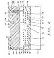
- FIG. 6shows a cross section of the interconnection scheme of the referenced continuation-in-part application invention.
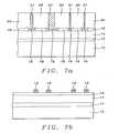
- FIG. 7 ashows a cross section of. a simplified version of the substrate and the layers that are created on the surface of the substrate under the processes of the referenced continuation-in-part application.
- FIG. 7 bshows the cross section of FIG. 7 a where an inductor has been added above the layer of passivation.
- FIG. 6is taken from related application U.S. patent application Ser. No. 09/251,183 and is herein incorporated by reference.
- FIG. 6there is shown a cross section of one implementation of the referenced application.
- the surface of silicon substrate 10has been provided with transistors and other devices (not shown in FIG. 6).
- the surface of substrate 10is covered by a dielectric layer 12 , layer 12 of dielectric is therefore deposited over the devices that have been provided in the surface of the substrate and over the substrate 10 .
- Conductive interconnect lines 11are provided inside layer 12 that connect to the semiconductor devices that have been provided in the surface of substrate 10 .
- Layers 14represent all of the metal layers and dielectric layers that are typically created on top of the dielectric layer 12 , layers 14 that are shown in FIG. 6 may therefore contain multiple layers of dielectric or insulation and the-like, conductive interconnect lines 13 make up the network of electrical connections that are created throughout layers 14 .
- Overlying and on the surface of layers 14are points 16 of electrical contact. These points 16 of electrical contact can for instance be bond pads that establish the electrical interconnects to the transistors and other devices that have been provided in the surface of the substrate 10 . These points of contact 16 are points of interconnect within the IC arrangement that need to be further connected to surrounding circuitry.
- a passivation layer 18formed of for example silicon nitride, is deposited over the surface of layer 14 to protect underlying layers from moisture, contamination, etc.
- the above referenced material that is used for the deposition of layer 20is polyimide
- the material that can be used for this layeris not limited to polyimide but can contain any of the known polymers (SiCl x O y ).
- the indicated polyimideis the preferred material to be used for the processes of the invention for the thick layer 20 of polymer.
- Examples of polymers that can be usedare silicons, carbons, fluoride, chlorides, oxygens, silicone elastomer, parylene or teflon, polycarbonate (PC), polysterene (PS), polyoxide (PO), poly polooxide (PPO), benzocyclobutene (BCB)
- Electrical contact with the contact points 16can now be established by filling the openings 22 / 36 / 38 with a conductive material.
- the top surfaces 24 of these metal conductors that are contained in openings 22 / 36 / 38can now be used for connection of the IC to its environment, and for further integration into the surrounding electrical circuitry.
- This latter statementis the same as saying the semiconductor devices that have been provided in the surface of substrate 10 can, via the conductive interconnects contained in openings 22 / 36 / 38 , be further connected to surrounding components arid circuitry.
- Interconnect pads 26 and 28are formed on top of surfaces 24 of the metal interconnects contained in poenings 22 , 36 and 38 . These pads 26 and 28 can be of any design requirements.
- a padcan, for instance, be used as a flip chip pad.
- Other padscan be used for power distribution or as a ground or signal bus.
- the following connectionscan, for instance, be made to the pads shown in FIG. 6: pad 26 can serve as a flip chip pad, pad 28 can serve as a flip chip pad or can be connected to electrical power or to electrical ground or to an electrical signal bus.
- pad size and the standard rules and restrictions of electrical circuit designdetermine the electrical connections to which a given pad lends itself.
- the pad sizecannot be too large since a large pad size brings with it a large capacitiance. In addition, a large pad size will interfere with the routine capability of that layer of metal. It is therefore preferred to keep the size of the pad 16 relatively small.
- the size of pad 16is however also directly related with the aspect ratio of vias 22 / 36 / 38 . An aspect ratio of about 5 is acceptable for the consideration of via etching and via filling. Based on these considerations, the size of the contact pad 16 can be in the order of 0.5 ⁇ m to 30 ⁇ m, the exact size being dependent on the thickness of layers 18 and 20 .
- the viasare filled with via plugs before the deposition of the metal layers 26 and 28 .
- the via plugsmay not be needed in which case the metal of layers 26 and 28 can directly establish contact with the pads 16 .
- Layer 18 in FIG. 6can be a typical IC passivation layer.
- the most frequently used passivation layer in the present state of the artis plasma enhanced CVD (PECVD) oxide and nitride.
- PECVDplasma enhanced CVD
- PECVD oxidecan be deposited first followed by a layer of approximately 0.7 um. nitride.
- Passivation layer 18is very important because it protects the device wafer from moisture and foreign ion contamination.
- the positioning of this layer between the sub-micron process (of the integrated circuit) and the lens-micron process (of the interconnecting metalization structure)is of critical importance since it allows for a cheaper process that possibly has less stringent clean room requirements for the process of creating the interconnecting metalization structure.
- Layer 20is a thick polymer dielectric layer (for example polyimide) that have a thickness in excess of 2 um (after curing).
- the range of the polymer thicknesscan vary from 2 um. to 150 um, dependent on electrical design requirements.
- the Hitachi-Dupont polyimide HD 2732 or 2734can, for example, be used.
- the polyimidecan be spin-on coated and cured. After spin-on coating, the polyimide will be cured at 400 degrees C. for 1 hour in a vacuum or nitrogen ambient. For thicker polyimide, the polyimide film can be multiple coated and cured.
- BCBpolymer benzocyclobutene
- openings 22 , 36 and 38have previously been discussed.
- the dimension of the opening together with the dielectric thicknessdetermine the aspect ratio of the opening.
- the aspect ratiochallenges the via etch process and the metal filling capability. This leads to a diameter for openings 22 / 36 / 38 in the range of approximately 0.5 um. to 30 um. the height for openings 22 / 36 / 38 can be in the range of approximately 2 um. to 150 um.
- the aspect ratio of openings 22 / 36 / 38is designed such that filling of the via with metal can be accomplished.
- the viacan be filled with CVD metal such as CVD tungsten or CVD copper, with electro-less nickel, with a damascene metal filling process, with electroplating copper, etc.
- the filling of the viasis not required as an extra processing step.
- a direct contactcan be established between the metal layers 26 and 28 and the contact pads 16 .
- the referenced applicationcan be further extended by applying multiple layers of polymer (such as polyimide) and can therefore be adapted to a larger variety of applications.
- the function of the structure that has been described in FIG. 6can be further extended by depositing a second layer of polyimide on top of the previously deposited layer 20 and overlaying the pads 26 and 28 .
- Selective etching and metal deposition or electro plating of metalcan further create additional contact points on the surface of the second layer of polyimide that can be interconnected with pads 26 and 28 .
- Additional layers of polyimide and the thereon created contact padscan be customized to a particular application, the indicated extension of multiple layers of polyimides greatly enhances the flexibility and usefulness of the referenced continuation-in-part application.
- FIG. 6shows a basic design advantage of the referenced continuation-in-part application. This advantage allows for the sub-micron or fine-lines, that run in the immediate vicinity of the metal layers 14 and the contact points 16 , to be extended in an upward direction 30 through metal interconnect 36 , this extension continues in the direction 32 in the horizontal plane of the metal interconnect 28 and comes back down in the downward direction 34 through metal interconnect 38 .
- the functions and constructs of the passivation layer 18 and the insulating layer 20remain as previously highlighted.
- This basic design advantage of the inventionis to “elevate” or “fan-out” the fine-line interconnects and to remove these interconnects from the micro and sub-micro level to a metal interconnect level that has considerably larger dimensions and that therefore has smaller resistance and capacitance and is easier and more cost effective to manufacture.
- This aspect of the referenced applicationdoes not include any aspect of pad re-distribution and therefore has an inherent quality of simplicity. It therefore further adds to the importance of the referenced application in that it makes micro and sub-micro wiring accessible at a wide and thick metal level.
- the interconnections 22 , 36 and 38interconnect the fine-level metal by going up through the passivation and polymer or polyimide dielectric layers, continuing over a distance on the wide and thick metal level and continuing by descending from the wide and thick metal level back down to the fine-metal level by again passing down through the passivation and polymer or polyimide dielectric layers.
- the extensions that are in this manner accomplishedneed not to be limited to extending fine-metal interconnect points 16 of any particular type, such as signal or power or ground, with wide and thick metal line 26 and 28 .
- the laws of physics and electronicswill impose limitations, if any, as to what type of interconnect can by established in this manner, limiting factors will be the conventional electrical limiting factors of resistance, propagation delay, RC constants and others.
- references continuation-in-part applicationprovides much broader latitude in being able to apply these laws and, in so doing, provides a considerably extended scope of the application and use of Integrated Circuits and the adaptation of these circuits to a wide and thick metal environment.
- FIG. 7 ashows, for reasons of clarity, a simplified cross section of the substrate and the layers that are created on the surface of the substrate under the processes of the invention, the highlighted areas that are shown have previously been identified as:
- [0065] 12is a layer of dielectric that has been deposited over the surface of the substrate
- [0066] 14is an interconnect layer that contains interconnect lines, vias and contact points
- [0067] 16are the contact points on the surface of the interconnect layer 14
- [0068] 18is a layer of passivation into which openings have been created through which the contact points 16 can be accessed
- [0069] 20is a thick layer of polymer
- [0070] 21are the conductive plugs that have been provided through the layer 20 of polyimide.
- the thick layer 20 of polymercan be coated in liquid form on the surface of the layer 18 of passivation or can be laminated over the surface of layer 18 of passivation by dry film application.
- Vias that are required for the creation of conductive plugs 21can be defined by conventional processes of photolithography or can be created using laser (drill) technology.
- Layer 12 of dielectricmay, in the cross section that is shown in FIG. 7 a , be part of layer 14 since layer 14 is a layer of Intra Level Dielectric (ILD) within which layer 12 can be readily integrated.
- ILDIntra Level Dielectric
- FIG. 7 bWith respect to the cross section that is shown in FIG. 7 b , the same layers that have been identified for FIG. 7 a are again provided in this cross section. Additionally has been shown the upper layer 17 of the silicon substrate 10 that contains active semiconductor devices. Also shown is cross section of an inductor 19 that has been created on the surface of layer 18 of passivation. It must again be emphasized that the ohmic resistivity of the metal that is used for the inductor 19 must be as low as possible.
- inductor 19For this reason, the use of a thick layer of for instance gold is preferred for the formation of inductor 19 , it has been shown that a thick layer of gold increased the Q value of inductor 19 from about 5 to about 20 for 2.4 GHz applications which represents a significant improvement in the Q value of inductor 19 .
- FIG. 3 athis figure refers only to power and ground pins and does not address signal or clock pins.
- FIG. 3 aa cross section of a silicon substrate 40 over which a interconnect network is created according to the invention, with a wide and thick wire interconnect network created in a thick layer of dielectric overlying a layer of passivation.
- a power and/or ground pinis provided through the surface of the thick layer of dielectric for external connection.
- [0075] 40is the silicon substrate on the surface of which interconnect lines are created in accordance with the invention
- [0076] 42are semiconductor circuits that are created in or on the surface of substrate 40
- [0077] 44is an ESD circuit that is provided for the protection of circuits 42
- connection pads 58are a layer of fine-line interconnects that has been created overlying connection pads 58 to the semiconductor devices 42
- 61is one of the vias that have been provided in layer 60 , more such vias are shown in FIG. 3 a but are, for reasons of simplicity, not highlighted
- [0081] 62is a layer of passivation that has been deposited overlying the layer 60 of fine-line interconnects
- 63is one of vias that passes through layer 62 of passivation, more such vias are shown in FIG. 3 a but are, for reasons of simplicity, not highlighted
- 64is a layer of dielectric in which, as a post-passivation process, interconnects have been created
- 65is a power or ground bus that is connected to the ESD circuit 44 , originating in layer 64 and further passing through layers 62 and 60
- [0085] 66is the combined (for multiple connection pads in layer 58 ) power or ground bus
- 67is a via that is created overlying the layer 62 of passivation, more such vias are shown in FIG. 3 a but are, for reasons of simplicity, not highlighted
- [0087] 68is the power of ground pin for the multiple semiconductor devices in layer 58 .
- [0092]provides, after ESD stimuli have passed through the ESD circuits, a fine-line interconnect network for further distribution of the power and ground stimuli, and
- the fine-line power and ground distribution networkis created underneath a layer of passivation.
- FIG. 3 acan be summarized as follows: a silicon substrate is provided in the surface of which have been created semiconductor devices and at least one electrostatic discharge (ESD) circuit, a first layer of dielectric is deposited over the substrate, a fine-line interconnect network is created in the first layer of dielectric making contact with the active circuits and the ESD circuit.
- ESDelectrostatic discharge
- a layer of passivationis deposited over the surface of the first layer of dielectric, a pattern of metal plugs (or, for low aspect ratio vias and as previously pointed out, direct interconnects between the overlying layers of metal) is created in the layer of passivation that aligns with points of contact created in the surface of the first layer of dielectric.
- a second layer of dielectricis deposited over the surface of the layer of passivation, a wide thick line interconnect network is created in said the layer of dielectric, contacting the ESD circuits.
- a point of electrical contactcomprising a power or ground contact is provided in the surface of said second layer of dielectric.
- FIG. 3 bprovides further insight into the creation of the power and ground interconnect lines of the invention whereby these interconnect lines have been shown as interconnect lines 66 and interconnect lines 66 ′.
- Interconnect lines 66have been created above the layer 62 of passivation and act as global power and ground interconnect lines.
- Interconnect lines 66 ′have been created below the layer 62 of passivation and act as local power and ground interconnect lines.
- FIG. 4 aaddresses the interconnections of signal and clock line.
- FIG. 4 athere is shown is a cross section of a silicon substrate 40 over which an interconnect network is created according to the invention.
- An access pin to an ESD circuit or driver or receiver circuits or I/O circuitsis provided through the surface of the layer of dielectric for external connection. While an ESD circuit is required for all circuits to which an I/O connection is established and independent of the type of circuit to which the I/O connection is established, the I/O interconnect can also be provided to a receiver circuit or a driver circuit or an I/O circuit.
- the inventionprovides a interconnect network comprising wide, thick interconnect lines for distribution of the clock and signal stimuli
- the inventioncreates a interconnect network of thick, wide interconnect lines for the clock and signal stimuli overlying a layer of passivation,
- [0104] 70is an external connection (pin) that is provided for the ESD circuit 45 and for driver/receiver/I/O circuit 45 ′, pin 70 provides external access for clock and signal stimuli to circuits 45 and 45 ′, and
- [0105] 72is a clock or signal bus that is created in the interconnect layer 64 using thick, wide wires for interconnect lines; it must be noted that the clock and signal interconnect line distribution is entirely contained within the layer 64 without providing an external point of I/O interconnect.
- the method that is used to create the interconnect network that is shown in cross section in FIG. 4 acan be summarized as follows.
- a silicon substrateis provided, active circuits have been created in the surface of the substrate including an ESD, receiver, driver and I/O circuit.
- First layers of dielectric of inorganic materialare deposited over the substrate, a fine-line interconnect network is created in the layers of dielectric, making contact with the active circuitry.
- a layer of passivationis deposited over the first thin layers of dielectric, a pattern of metal plugs is created in the layer of passivation (or, for low aspect ratio openings, direct contact is established between overlying layers of metal through an opening in an interposed layer of dielectric), the metal interconnects align with points of electrical contact in the surface of the first layers of dielectric.
- One or more thicker layers of dielectricare deposited over the surface of the layer of passivation, typically of an organic material, a wide thick line interconnect network is created in the thicker layer of dielectric, making electrical contact with the metal plugs or the metal pads in or under the layer of passivation, including to the one ESD, receiver, driver or I/O circuit.
- a point of electrical contactis provided in the surface of the second layer of dielectric to the ESD, receiver, driver or I/O circuit.
- FIG. 4 bprovides further insight into the creation of the signal and clock interconnect lines of the invention whereby these interconnect lines have been shown as interconnect lines 71 and interconnect lines 71 ′.
- Interconnect lines 71have been created above the layer 62 of passivation and act as global signal and clock interconnect lines.
- Interconnect lines 71 ′have been created below the layer 62 of passivation and act as local signal and clock interconnect lines.
- FIG. 5 ashows a cross section of a silicon substrate 40 over which a interconnect network is created according to the invention, with the interconnect network created in a thick layer of dielectric overlying a layer of passivation and remaining internal to the thick layer of dielectric. No ESD, receiver, driver or I/O circuit access pin is provided through the surface of the layer of dielectric for external connection. Shown in FIG. 5 a and not previously highlighted is the clock or signal interconnect line 74 , providing for an interconnect scheme of thick, wide lines overlying a passivation layer whereby no external I/O connections are provided.
- each thick, wide interconnect line(where such thick, wide interconnect lines are used) must be provided with at least one I/O connect point for off-chip connection.
- the method that is used to create the wide thick line interconnect lines that is shown in cross section in FIG. 5 acan be summarized as follows and is similar to that described above for FIG. 4 a .
- a silicon substrateis provided, active devices have been provided in the surface of the substrate.
- First thin layers of dielectricare deposited over the surface of the substrate, a fine-line interconnect network is created in the first layers of dielectric comprising fine-line interconnect lines, making contact with points of electrical contact in the surface of the substrate.
- a layer of passivationis deposited over the surface of the first layers of dielectric, a pattern of conductive interconnects is created in the layer of passivation that aligns with the points of electrical contact in the surface of the first layer of dielectric.
- One or more second layers of dielectricare deposited over the surface of the layer of passivation, making electrical contact with the conductive interconnects in the layer of passivation.
- FIG. 5 bprovides further insight into the creation of the signal and clock interconnect lines of the invention whereby these interconnect lines have been shown as interconnect lines 74 and interconnect lines 74 ′.
- Interconnect lines 74have been created above the layer 62 of passivation and can act as global signal and clock interconnect lines.
- Interconnect lines 74 ′have been created below the layer 62 of passivation and act as local signal and clock interconnect lines.
- FIGS. 3 - 5show a fine-line interconnect network 60 that underlies the layer 62 of passivation
- the inventionalso enables and can be further extended with the complete elimination of the fine-line interconnect network 60 and creating an interconnect network 64 that uses only thick, wide wires.
- the first layer of dielectric 60is not applied, the layer 62 of passivation is deposited directly over the surface of the created semiconductor devices 58 in or on the surface of substrate 40 .
- the fine-line interconnect linesare typically created in a layer of inorganic dielectric
- the thick wide interconnect linesare typically created in a layer of dielectric comprising polymer. This because an inorganic material cannot be deposited as a thick layer of dielectric because such a layer of dielectric would develop fissures and crack as a result
- fine-line interconnect metalis typically created using methods of sputter with resist etching or of damascene processes using oxide etch with electroplating after which CMP is applied. Either one of these two approaches cannot create thick metal due to cost considerations or oxide cracking
- thick, wide interconnect linescan be created by first sputtering a thin metal base layer, coating and patterning a thick layer of photoresist, applying a thick layer of metal by electroplating, removing the patterned photoresist and performing metal base etching (of the sputtered thin metal base).
- This methodallows for the creation of a pattern of very thick metal, metal thickness in excess of 1 ⁇ m can in this manner be achieved while the thickness of the layer of dielectric in which the thick metal interconnect lines are created can be in excess of 2 ⁇ m.
Landscapes
- Engineering & Computer Science (AREA)
- Power Engineering (AREA)
- Physics & Mathematics (AREA)
- Computer Hardware Design (AREA)
- Microelectronics & Electronic Packaging (AREA)
- Condensed Matter Physics & Semiconductors (AREA)
- General Physics & Mathematics (AREA)
- Geometry (AREA)
- Manufacturing & Machinery (AREA)
- Internal Circuitry In Semiconductor Integrated Circuit Devices (AREA)
- Semiconductor Integrated Circuits (AREA)
- Formation Of Insulating Films (AREA)
Abstract
Description
- This application is related to U.S. patent application Ser. No. 09/251,183 filed on Feb. 17, 1999 which is a continuation-in-part of U.S. patent application Ser. No. 09/216,791 filed on Dec. 21, 1998, assigned to a common assignee. This application is also related to attorney docket MEG00-008, serial number ______, filing date ______.[0001]
- (1) Field of the Invention[0002]
- The invention relates to the fabrication of integrated circuit devices, and more particularly, to a method of post-passivation processing for the creation of conductive interconnects.[0003]
- (2) Description of the Prior Art[0004]
- Improvements in semiconductor device performance are typically obtained by scaling down the geometric dimensions of the Integrated Circuits, this results in a decrease in the cost per die while at the same time some aspects of semiconductor device performance are improved. The metal connections which connect the Integrated Circuit to other circuit or system components become of relative more importance and have, with the further miniaturization of the IC, an increasingly negative impact on the circuit performance. The parasitic capacitance and resistance of the metal interconnections increase, which degrades the chip performance significantly. Of most concern in this respect is the voltage drop along the power and ground buses and the RC delay of the critical signal paths. Attempts to reduce the resistance by using wider metal lines result in higher capacitance of these wires.[0005]
- To solve this problem, one approach has been is to develop low resistance metal (such as copper) for the wires while low dielectric materials are used in between signal lines. Current practice is to create metal interconnection networks under a layer of passivation, this approach however limits the interconnect network to fine line interconnects and the therewith associated how parasitic capacitance and high line resistivity. The latter two parameters, because of their relatively high values, degrade device performance, an effect which becomes even more severe for higher frequency applications and for long interconnect lines that are, for instance, used for clock distribution lines. Also, fine line interconnect metal cannot carry high values of current that is typically needed for ground busses and for power busses.[0006]
- It has previously been stated that it is of interest to the semiconductor art to provide a method of creating interconnect lines that removes typical limitations that are imposed on the interconnect wires, such as unwanted parasitic capacitances and high interconnect line resistivity. The invention provides such a method. An analogy can be drawn in this respect whereby the currently (prior art) used fine-line interconnection schemes, which are created under a layer of passivation, are the streets in a city; in the post-passivation interconnection scheme of the present invention, the interconnections that are created above a layer of passivation can be considered the freeways between cities.[0007]
- FIG. 1 shows a cross section of a silicon substrate on the surface of which has been created a conductive interconnect network. The structure that is shown in cross section in FIG. 1 addresses only and is limited to prior art power and ground distribution networks. The various features that have been highlighted in FIG. 1 are the following:[0008]
- [0009]40, a silicon substrate on the surface of which has been created an interconnect network
- [0010]42, a sample number of semiconductor circuits that have been created in or on the surface of the
substrate 40 - [0011]44, two electrostatic discharge (ESD) circuits created in or on the surface of the
substrate 40, one ESD circuit is provided for each pin that is accessible for external connections (pins 52, see below) - [0012]46 is a layer of interconnect lines; these interconnect lines are above the surface of
substrate 40 and under the layer48 of passivation and represent a typical application of prior art fine-line interconnects; these fine-line interconnect oflayer 46 typically have high resistivity and high parasitic capacitance - [0013]48 is a layer of passivation that is deposited over the surface of the
layer 46 of interconnect lines - [0014]50 is a power or ground bus that connects to the
circuits 42 via fine-line interconnect lines provided inlayer 46; this power or ground bus is typically of wider metal since this power or ground bus carries the accumulated current or ground connection for thedevices 42 - [0015]52 is a power or ground pin that passes through the layer48 of passivation and that has been connected to the power or
ground bus 50. - From the above the following can be summarized: circuits are created in or on the surface of a silicon substrate, interconnect lines are created for these circuits for further interconnection to external circuitry, the circuits are, on a per I/O pin basis, provided with an ESD circuit, these circuits with their ESD circuit are connected to a power or ground pin that penetrates a layer of passivation. The layer of passivation is the final layer that overlies the created interconnect line structure, the interconnect line underneath the layer of passivation are fine line interconnects and have all the electrical disadvantages of fine line interconnects such as high resistivity and high parasitic capacitance.[0016]
- Relating to the cross section that is shown in FIG. 1, the following comments applies: ESD circuits are, as is known in the art, provided for the protection of semiconductor circuits against unexpected electrical charges. For this reason, each pin that connects to a semiconductor circuit must be provided with an ESD circuit.[0017]
- FIG. 2 shows a cross section of a prior art configuration that resembles the cross section shown in FIG. 1. The structure that is shown in cross section in FIG. 2 however addresses only and is limited to clock and signal distribution networks. FIG. 2 shows in addition (to the previously highlighted aspects of FIG. 1):[0018]
- [0019]45 are two ESD circuits that are provided in or on the surface of the
substrate 40; ESD circuits are always required for any external connection to an input/output (I/O) pin - [0020]45′ which are circuits that can be receiver or driver or I/O circuits for input (receiver) or output (driver) or I/O purposes respectively
- [0021]54 is a clock bus
- [0022]56 is a clock or signal pin that has been extended through the layer48 of passivation.
- The same comments apply to the cross section that is shown in FIG. 2 as previously have been made with respect to FIG. 1, with as a summary statement that the layer of passivation is the final layer that overlies the created structure, the interconnect lines underneath the layer of passivation are fine line interconnects and have all the electrical disadvantages of fine line interconnects such as high resistivity and high parasitic capacitance.[0023]
- Further applies to the cross section that is shown in FIG. 2, where[0024]
pins 56 are signal or clock pins: - [0025]
pins 56 must be connected to ESD and driver/receiver or I/O circuits 45 - for signal or[0026]
clock pins 56, these pins must be connected not only to ESD circuits but also to driver or receiver or I/O circuits, highlighted ascircuit 45′ in FIG. 2 - after (clock and signal) stimuli have passed through the ESD and driver/receiver or I/O circuits, these stimuli are further routed using, under prior art methods, fine-line interconnect wires. A layer of passivation is deposited over the dielectric layer in which the interconnect network has been created.[0027]
- It is therefore of interest to the semiconductor art to provide a method of creating interconnect lines that removes typical limitations that are imposed on the interconnect wires, such as unwanted parasitic capacitances and high interconnect line resistivity.[0028]
- A principal objective of the invention is to provide a method for the creation of interconnect metal that allows for the use of thick and wide metal.[0029]
- Another objective of the invention is to provide a method for the creation of interconnect metal that uses the application of thick layer of dielectric such as polymer.[0030]
- Yet another objective of the invention is to provide a method that allows for the creation of long interconnect lines, whereby these long interconnect lines do not have high resistance or introduce high parasitic capacitance.[0031]
- A still further objective of the invention is to create interconnect lines that can carry high values of current for the creation of power and ground distribution networks.[0032]
- A still further objective of the invention is to create interconnect metal that can be created using cost effective methods of manufacturing by creating the interconnect metal on the surface of and after a layer of passivation has been deposited.[0033]
- In accordance with the objectives of the invention a new method is provided for the creation of interconnect lines. Fine line interconnects are provided in a first layer of dielectric overlying semiconductor circuits that have been created in or on the surface of a substrate. A layer of passivation is deposited over the layer of dielectric, a thick second layer of dielectric is created over the surface of the layer of passivation. Thick and wide interconnect lines are created in the thick second layer of dielectric.[0034]
- FIG. 1 is a cross section of a silicon substrate over which a prior art fine-line interconnect network is created over which a layer of passivation is deposited, power and/or ground pins are provided through the layer of passivation for external connection. The structure that is shown in cross section in FIG. 1 addresses only and is limited-to prior art power and ground distribution networks.[0035]
- FIG. 2 is a cross section of a silicon substrate over which a prior art fine-line interconnect network is created over which a layer of passivation is deposited, clock and/or signal pins are provided through the layer of passivation for external connection. The structure that is shown in cross section in FIG. 2 addresses only and is limited to prior art clock and signal distribution networks.[0036]
- FIG. 3[0037]ais a cross section of a silicon substrate over which an interconnect network is created according to the invention. Power and/or ground pins are provided through the surface of the layer of dielectric for external connection. The structure that is shown in cross section in FIGS. 3aand3baddresses only and is limited to power and ground distribution networks of the invention.
- FIG. 3[0038]bdifferentiates between power and ground distribution lines that are below a layer of passivation and power and ground distribution lines that are above a layer of passivation.
- FIG. 4[0039]ais a cross section of a silicon substrate over which an interconnect network is created according to the invention. An ESD and/or driver and/or receiver circuit access pin is provided through the surface of the layer of dielectric for external connection. The structure that is shown in cross section in FIGS. 4aand4baddresses only and is limited to clock and signal distribution networks of the invention.
- FIG. 4[0040]bdifferentiates between clock and signal distribution lines that are below a layer of passivation and clock and signal distribution lines that are above a layer of passivation.
- FIG. 5[0041]ais a cross section of a silicon substrate over which an interconnect network is created according to the invention. No I/O connect pin is provided through the surface of the layer of dielectric for external connection. The structure that is shown in cross section in FIGS. 4aand4baddresses only and is limited to clock and signal distribution networks of the invention.
- FIG. 5[0042]bdifferentiates between clock and signal distribution lines that are below a layer of passivation and clock and signal distribution lines that are above a layer of passivation.
- FIG. 6 shows a cross section of the interconnection scheme of the referenced continuation-in-part application invention.[0043]
- FIG. 7[0044]ashows a cross section of. a simplified version of the substrate and the layers that are created on the surface of the substrate under the processes of the referenced continuation-in-part application.
- FIG. 7[0045]bshows the cross section of FIG. 7awhere an inductor has been added above the layer of passivation.
- For purposes of reference and for clarity of understanding, FIG. 6, is taken from related application U.S. patent application Ser. No. 09/251,183 and is herein incorporated by reference.[0046]
- Referring now more specifically to FIG. 6, there is shown a cross section of one implementation of the referenced application. The surface of[0047]
silicon substrate 10 has been provided with transistors and other devices (not shown in FIG. 6). The surface ofsubstrate 10 is covered by adielectric layer 12,layer 12 of dielectric is therefore deposited over the devices that have been provided in the surface of the substrate and over thesubstrate 10.Conductive interconnect lines 11 are provided insidelayer 12 that connect to the semiconductor devices that have been provided in the surface ofsubstrate 10. - Layers[0048]14 (two examples are shown) represent all of the metal layers and dielectric layers that are typically created on top of the
dielectric layer 12, layers14 that are shown in FIG. 6 may therefore contain multiple layers of dielectric or insulation and the-like,conductive interconnect lines 13 make up the network of electrical connections that are created throughoutlayers 14. Overlying and on the surface oflayers 14 arepoints 16 of electrical contact. Thesepoints 16 of electrical contact can for instance be bond pads that establish the electrical interconnects to the transistors and other devices that have been provided in the surface of thesubstrate 10. These points ofcontact 16 are points of interconnect within the IC arrangement that need to be further connected to surrounding circuitry. Apassivation layer 18, formed of for example silicon nitride, is deposited over the surface oflayer 14 to protect underlying layers from moisture, contamination, etc. - The key steps of the above referenced application begin with the deposition of a[0049]
thick layer 20 of polyimide that is deposited over the surface oflayer 18. Access must be provided to points ofelectrical contact 16, for this reason a pattern ofopenings polyimide layer 20 and thepassivation layer 18, the pattern ofopenings openings 22/36/38 that are created in thelayer 20 of polyimide, electrically extended to the surface oflayer 20. - The above referenced material that is used for the deposition of[0050]
layer 20 is polyimide, the material that can be used for this layer is not limited to polyimide but can contain any of the known polymers (SiClxOy). The indicated polyimide is the preferred material to be used for the processes of the invention for thethick layer 20 of polymer. Examples of polymers that can be used are silicons, carbons, fluoride, chlorides, oxygens, silicone elastomer, parylene or teflon, polycarbonate (PC), polysterene (PS), polyoxide (PO), poly polooxide (PPO), benzocyclobutene (BCB) - Electrical contact with the contact points[0051]16 can now be established by filling the
openings 22/36/38 with a conductive material. The top surfaces24 of these metal conductors that are contained inopenings 22/36/38 can now be used for connection of the IC to its environment, and for further integration into the surrounding electrical circuitry. This latter statement is the same as saying the semiconductor devices that have been provided in the surface ofsubstrate 10 can, via the conductive interconnects contained inopenings 22/36/38, be further connected to surrounding components arid circuitry.Interconnect pads surfaces 24 of the metal interconnects contained inpoenings pads pad 28 can serve as a flip chip pad or can be connected to electrical power or to electrical ground or to an electrical signal bus. There is no connection between the size of the pads shown in FIG. 6 and the suggested possible electrical connections for which this pad can be used. Pad size and the standard rules and restrictions of electrical circuit design determine the electrical connections to which a given pad lends itself. - The following comments relate to the size and the number of the contact points[0052]16, FIG. 6. Because these contact points16 are located on top of a thin dielectric (
layer 14, FIG. 6) the pad size cannot be too large since a large pad size brings with it a large capacitiance. In addition, a large pad size will interfere with the routine capability of that layer of metal. It is therefore preferred to keep the size of thepad 16 relatively small. The size ofpad 16 is however also directly related with the aspect ratio ofvias 22/36/38. An aspect ratio of about 5 is acceptable for the consideration of via etching and via filling. Based on these considerations, the size of thecontact pad 16 can be in the order of 0.5 μm to 30 μm, the exact size being dependent on the thickness oflayers - For higher aspect ratio vias, the vias are filled with via plugs before the deposition of the metal layers[0053]26 and28. However, for vias that have lower aspect ratios (for example less than 2), the via plugs may not be needed in which case the metal of
layers pads 16. - The referenced application does not impose a limitation on the number of contact pads that can be included in the design, this number is not only dependent on package design requirements but is mostly dependent on the internal circuit design requirements of the package.[0054]
Layer 18 in FIG. 6 can be a typical IC passivation layer. - The most frequently used passivation layer in the present state of the art is plasma enhanced CVD (PECVD) oxide and nitride. In creating[0055]
layer 18 of passivation, a layer of approximately 0.5 um. PECVD oxide can be deposited first followed by a layer of approximately 0.7 um. nitride.Passivation layer 18 is very important because it protects the device wafer from moisture and foreign ion contamination. The positioning of this layer between the sub-micron process (of the integrated circuit) and the lens-micron process (of the interconnecting metalization structure) is of critical importance since it allows for a cheaper process that possibly has less stringent clean room requirements for the process of creating the interconnecting metalization structure. - [0056]
Layer 20 is a thick polymer dielectric layer (for example polyimide) that have a thickness in excess of 2 um (after curing). The range of the polymer thickness can vary from 2 um. to 150 um, dependent on electrical design requirements. - For the deposition of[0057]
layer 20 the Hitachi-Dupont polyimide HD 2732 or 2734 can, for example, be used. The polyimide can be spin-on coated and cured. After spin-on coating, the polyimide will be cured at 400 degrees C. for 1 hour in a vacuum or nitrogen ambient. For thicker polyimide, the polyimide film can be multiple coated and cured. - Another material that can be used to create[0058]
layer 20 is the polymer benzocyclobutene (BCB). This polymer is at this time commercially produced by for instance Dow Chemical and has recently gained acceptance to be used instead of typical polyimide application. - The dimensions of[0059]
openings openings 22/36/38 in the range of approximately 0.5 um. to 30 um. the height foropenings 22/36/38 can be in the range of approximately 2 um. to 150 um. The aspect ratio ofopenings 22/36/38 is designed such that filling of the via with metal can be accomplished. The via can be filled with CVD metal such as CVD tungsten or CVD copper, with electro-less nickel, with a damascene metal filling process, with electroplating copper, etc. As previously stated, for low aspect ratio vias, the filling of the vias is not required as an extra processing step. A direct contact can be established between the metal layers26 and28 and thecontact pads 16. - The referenced application can be further extended by applying multiple layers of polymer (such as polyimide) and can therefore be adapted to a larger variety of applications. The function of the structure that has been described in FIG. 6 can be further extended by depositing a second layer of polyimide on top of the previously deposited[0060]
layer 20 and overlaying thepads pads - FIG. 6 shows a basic design advantage of the referenced continuation-in-part application. This advantage allows for the sub-micron or fine-lines, that run in the immediate vicinity of the metal layers[0061]14 and the contact points16, to be extended in an
upward direction 30 throughmetal interconnect 36, this extension continues in the direction32 in the horizontal plane of themetal interconnect 28 and comes back down in the downward direction34 throughmetal interconnect 38. The functions and constructs of thepassivation layer 18 and the insulatinglayer 20 remain as previously highlighted. This basic design advantage of the invention is to “elevate” or “fan-out” the fine-line interconnects and to remove these interconnects from the micro and sub-micro level to a metal interconnect level that has considerably larger dimensions and that therefore has smaller resistance and capacitance and is easier and more cost effective to manufacture. This aspect of the referenced application does not include any aspect of pad re-distribution and therefore has an inherent quality of simplicity. It therefore further adds to the importance of the referenced application in that it makes micro and sub-micro wiring accessible at a wide and thick metal level. Theinterconnections thick metal line - This completes the discussion of the construct shown for purposes of reference in FIG. 6. Following will further be discussed the cross sections that are shown in FIGS. 7[0062]aand7b.
- FIG. 7[0063]ashows, for reasons of clarity, a simplified cross section of the substrate and the layers that are created on the surface of the substrate under the processes of the invention, the highlighted areas that are shown have previously been identified as:
- [0064]10 the silicon substrate
- [0065]12 is a layer of dielectric that has been deposited over the surface of the substrate
- [0066]14 is an interconnect layer that contains interconnect lines, vias and contact points
- [0067]16 are the contact points on the surface of the
interconnect layer 14 - [0068]18 is a layer of passivation into which openings have been created through which the contact points16 can be accessed
- [0069]20 is a thick layer of polymer, and
- [0070]21 are the conductive plugs that have been provided through the
layer 20 of polyimide. - The[0071]
thick layer 20 of polymer can be coated in liquid form on the surface of thelayer 18 of passivation or can be laminated over the surface oflayer 18 of passivation by dry film application. Vias that are required for the creation ofconductive plugs 21 can be defined by conventional processes of photolithography or can be created using laser (drill) technology. - It is clear from previous discussions that the sequence of layers that is shown in cross section in FIG. 7[0072]ahas been created so that additional electrical components such as an inductor, a capacitor and the like can be created on the surface of
layer 20 of polyimide and in electrical contact withconductive plugs 21.Layer 12 of dielectric may, in the cross section that is shown in FIG. 7a, be part oflayer 14 sincelayer 14 is a layer of Intra Level Dielectric (ILD) within whichlayer 12 can be readily integrated. - With respect to the cross section that is shown in FIG. 7[0073]b, the same layers that have been identified for FIG. 7aare again provided in this cross section. Additionally has been shown the
upper layer 17 of thesilicon substrate 10 that contains active semiconductor devices. Also shown is cross section of aninductor 19 that has been created on the surface oflayer 18 of passivation. It must again be emphasized that the ohmic resistivity of the metal that is used for theinductor 19 must be as low as possible. For this reason, the use of a thick layer of for instance gold is preferred for the formation ofinductor 19, it has been shown that a thick layer of gold increased the Q value ofinductor 19 from about 5 to about 20 for 2.4 GHz applications which represents a significant improvement in the Q value ofinductor 19. - Referring now specifically to FIG. 3[0074]a, this figure refers only to power and ground pins and does not address signal or clock pins. There is shown in FIG. 3aa cross section of a
silicon substrate 40 over which a interconnect network is created according to the invention, with a wide and thick wire interconnect network created in a thick layer of dielectric overlying a layer of passivation. A power and/or ground pin is provided through the surface of the thick layer of dielectric for external connection. Following are the various features that are shown in FIG. 3a: - [0075]40 is the silicon substrate on the surface of which interconnect lines are created in accordance with the invention
- [0076]42 are semiconductor circuits that are created in or on the surface of
substrate 40 - [0077]44 is an ESD circuit that is provided for the protection of
circuits 42 - [0078]58 are connection pads to the
semiconductor devices 42 that have been created in or on the surface ofsubstrate 40 - [0079]60 is a layer of fine-line interconnects that has been created
overlying connection pads 58 to thesemiconductor devices 42 - [0080]61 is one of the vias that have been provided in
layer 60, more such vias are shown in FIG. 3abut are, for reasons of simplicity, not highlighted - [0081]62 is a layer of passivation that has been deposited overlying the
layer 60 of fine-line interconnects - [0082]63 is one of vias that passes through
layer 62 of passivation, more such vias are shown in FIG. 3abut are, for reasons of simplicity, not highlighted - [0083]64 is a layer of dielectric in which, as a post-passivation process, interconnects have been created
- [0084]65 is a power or ground bus that is connected to the
ESD circuit 44, originating inlayer 64 and further passing throughlayers - [0085]66 is the combined (for multiple connection pads in layer58) power or ground bus
- [0086]67 is a via that is created overlying the
layer 62 of passivation, more such vias are shown in FIG. 3abut are, for reasons of simplicity, not highlighted - [0087]68 is the power of ground pin for the multiple semiconductor devices in
layer 58. - From the cross section that is shown in FIG. 3[0088]a, its is clear that, most importantly, the ability to create interconnects to semiconductor devices that have been created in or on the surface of a substrate has been extended by creating these interconnects not only in as fine-line interconnects in
layer 60 but extending the interconnect by creation a wide, thick wire interconnect network overlying a layer of passivation. This provides immediate and significant benefits in that these lines are further removed from the surface of the substrate (reducing parasitic influences by the interconnect lines on the semiconductor devices that are created in or on the surface of the substrate) while the interconnect network that is created overlying the layer of passivation can now contains sturdier, that is thicker and wider, interconnect lines. The thick, wide metal interconnects can be used for power and ground distribution, this distribution than takes place above a layer of passivation and partially replaces and extends the conventional method of having for these purposes a fine-line distribution interconnect network under the layer of passivation. - Some points of interest can be listed at this time as they relate to prior art methods and to the invention.[0089]
- Prior Art:[0090]
- provides an ESD circuit for each pin that is used for external input/output interconnect[0091]
- provides, after ESD stimuli have passed through the ESD circuits, a fine-line interconnect network for further distribution of the power and ground stimuli, and[0092]
- the fine-line power and ground distribution network is created underneath a layer of passivation.[0093]
- It must, in this respect and related to the above provided comments, be remembered that power and ground pins do not require drivers and/or receiver circuitry.[0094]
- The invention:[0095]
- does not need to create an ESD circuit for each pin that is used for external input/output interconnect; this in view of the more robust wiring that drives the ESD circuit, resulting in reduced power loss by an unexpected power surge over the interconnect line, resulting in more power being delivered to the ESD circuit, and[0096]
- allows for the power and ground interconnects to be directly connected to the internal circuits of a semiconductor device, this either without an ESD circuit or with a smaller than regular ESD circuit (as previously explained).[0097]
- The method that is used to create the interconnect network that is shown in cross section in FIG. 3[0098]aaddresses only the use of power and ground connections and does not apply to clock and signal interconnect lines. FIG. 3acan be summarized as follows: a silicon substrate is provided in the surface of which have been created semiconductor devices and at least one electrostatic discharge (ESD) circuit, a first layer of dielectric is deposited over the substrate, a fine-line interconnect network is created in the first layer of dielectric making contact with the active circuits and the ESD circuit. A layer of passivation is deposited over the surface of the first layer of dielectric, a pattern of metal plugs (or, for low aspect ratio vias and as previously pointed out, direct interconnects between the overlying layers of metal) is created in the layer of passivation that aligns with points of contact created in the surface of the first layer of dielectric. A second layer of dielectric is deposited over the surface of the layer of passivation, a wide thick line interconnect network is created in said the layer of dielectric, contacting the ESD circuits. A point of electrical contact comprising a power or ground contact is provided in the surface of said second layer of dielectric.
- FIG. 3[0099]bprovides further insight into the creation of the power and ground interconnect lines of the invention whereby these interconnect lines have been shown as
interconnect lines 66 andinterconnect lines 66′.Interconnect lines 66 have been created above thelayer 62 of passivation and act as global power and ground interconnect lines.Interconnect lines 66′ have been created below thelayer 62 of passivation and act as local power and ground interconnect lines. - Referring now to FIG. 4[0100]a, FIG. 4aaddresses the interconnections of signal and clock line. In FIG. 4athere is shown is a cross section of a
silicon substrate 40 over which an interconnect network is created according to the invention. An access pin to an ESD circuit or driver or receiver circuits or I/O circuits is provided through the surface of the layer of dielectric for external connection. While an ESD circuit is required for all circuits to which an I/O connection is established and independent of the type of circuit to which the I/O connection is established, the I/O interconnect can also be provided to a receiver circuit or a driver circuit or an I/O circuit. - The not previously highlighted features that are shown in FIG. 4[0101]aare:
- the invention provides a interconnect network comprising wide, thick interconnect lines for distribution of the clock and signal stimuli[0102]
- the invention creates a interconnect network of thick, wide interconnect lines for the clock and signal stimuli overlying a layer of passivation,[0103]
- [0104]70 is an external connection (pin) that is provided for the
ESD circuit 45 and for driver/receiver/I/O circuit 45′,pin 70 provides external access for clock and signal stimuli tocircuits - [0105]72 is a clock or signal bus that is created in the
interconnect layer 64 using thick, wide wires for interconnect lines; it must be noted that the clock and signal interconnect line distribution is entirely contained within thelayer 64 without providing an external point of I/O interconnect. - The method that is used to create the interconnect network that is shown in cross section in FIG. 4[0106]acan be summarized as follows. A silicon substrate is provided, active circuits have been created in the surface of the substrate including an ESD, receiver, driver and I/O circuit. First layers of dielectric of inorganic material are deposited over the substrate, a fine-line interconnect network is created in the layers of dielectric, making contact with the active circuitry. A layer of passivation is deposited over the first thin layers of dielectric, a pattern of metal plugs is created in the layer of passivation (or, for low aspect ratio openings, direct contact is established between overlying layers of metal through an opening in an interposed layer of dielectric), the metal interconnects align with points of electrical contact in the surface of the first layers of dielectric. One or more thicker layers of dielectric are deposited over the surface of the layer of passivation, typically of an organic material, a wide thick line interconnect network is created in the thicker layer of dielectric, making electrical contact with the metal plugs or the metal pads in or under the layer of passivation, including to the one ESD, receiver, driver or I/O circuit. A point of electrical contact is provided in the surface of the second layer of dielectric to the ESD, receiver, driver or I/O circuit.
- FIG. 4[0107]bprovides further insight into the creation of the signal and clock interconnect lines of the invention whereby these interconnect lines have been shown as
interconnect lines 71 andinterconnect lines 71′.Interconnect lines 71 have been created above thelayer 62 of passivation and act as global signal and clock interconnect lines.Interconnect lines 71′ have been created below thelayer 62 of passivation and act as local signal and clock interconnect lines. - FIG. 5[0108]ashows a cross section of a
silicon substrate 40 over which a interconnect network is created according to the invention, with the interconnect network created in a thick layer of dielectric overlying a layer of passivation and remaining internal to the thick layer of dielectric. No ESD, receiver, driver or I/O circuit access pin is provided through the surface of the layer of dielectric for external connection. Shown in FIG. 5aand not previously highlighted is the clock orsignal interconnect line 74, providing for an interconnect scheme of thick, wide lines overlying a passivation layer whereby no external I/O connections are provided. Due to the thick, wide lines of the interconnect network that is created overlying a passivation layer, the clock and signal distribution can take place entirely within theinterconnect layer 64, this as opposed to prior art methods where, for clock and signal distribution lines, each thick, wide interconnect line (where such thick, wide interconnect lines are used) must be provided with at least one I/O connect point for off-chip connection. - The method that is used to create the wide thick line interconnect lines that is shown in cross section in FIG. 5[0109]acan be summarized as follows and is similar to that described above for FIG. 4a. A silicon substrate is provided, active devices have been provided in the surface of the substrate. First thin layers of dielectric are deposited over the surface of the substrate, a fine-line interconnect network is created in the first layers of dielectric comprising fine-line interconnect lines, making contact with points of electrical contact in the surface of the substrate. A layer of passivation is deposited over the surface of the first layers of dielectric, a pattern of conductive interconnects is created in the layer of passivation that aligns with the points of electrical contact in the surface of the first layer of dielectric. One or more second layers of dielectric are deposited over the surface of the layer of passivation, making electrical contact with the conductive interconnects in the layer of passivation.
- FIG. 5[0110]bprovides further insight into the creation of the signal and clock interconnect lines of the invention whereby these interconnect lines have been shown as
interconnect lines 74 andinterconnect lines 74′.Interconnect lines 74 have been created above thelayer 62 of passivation and can act as global signal and clock interconnect lines.Interconnect lines 74′ have been created below thelayer 62 of passivation and act as local signal and clock interconnect lines. - It must further be emphasized that, where FIGS.[0111]3-5 show a fine-
line interconnect network 60 that underlies thelayer 62 of passivation, the invention also enables and can be further extended with the complete elimination of the fine-line interconnect network 60 and creating aninterconnect network 64 that uses only thick, wide wires. For this application of the invention, the first layer ofdielectric 60 is not applied, thelayer 62 of passivation is deposited directly over the surface of the createdsemiconductor devices 58 in or on the surface ofsubstrate 40. - It is further of value to briefly discuss the above implemented and addressed distinction between fine-line interconnect lines and wide, thick interconnect lines. The following points apply in this respect:[0112]
- the prior art fine line interconnect lines are created underneath a layer of passivation, the wide, thick interconnect lines of the invention are created above a layer of passivation[0113]
- the fine-line interconnect lines are typically created in a layer of inorganic dielectric, the thick wide interconnect lines are typically created in a layer of dielectric comprising polymer. This because an inorganic material cannot be deposited as a thick layer of dielectric because such a layer of dielectric would develop fissures and crack as a result[0114]
- fine-line interconnect metal is typically created using methods of sputter with resist etching or of damascene processes using oxide etch with electroplating after which CMP is applied. Either one of these two approaches cannot create thick metal due to cost considerations or oxide cracking[0115]
- thick, wide interconnect lines can be created by first sputtering a thin metal base layer, coating and patterning a thick layer of photoresist, applying a thick layer of metal by electroplating, removing the patterned photoresist and performing metal base etching (of the sputtered thin metal base). This method allows for the creation of a pattern of very thick metal, metal thickness in excess of 1 μm can in this manner be achieved while the thickness of the layer of dielectric in which the thick metal interconnect lines are created can be in excess of 2 μm.[0116]
- Although the invention has been described and illustrated with reference to specific illustrative embodiments thereof, it is not intended that the invention be limited to those illustrative embodiments. Those skilled in the art will recognize that variations and modifications can be made without departing from the spirit of the invention. It is therefore intended to include within the invention all such variations and modifications which fall within the scope of the appended claims and equivalents thereof.[0117]
Claims (46)
Priority Applications (36)
| Application Number | Priority Date | Filing Date | Title |
|---|---|---|---|
| US10/278,106US6734563B2 (en) | 2000-10-18 | 2002-10-22 | Post passivation interconnection schemes on top of the IC chips |
| US10/653,628US7443033B2 (en) | 1998-12-21 | 2003-09-02 | Post passivation interconnection schemes on top of the IC chips |
| US10/685,872US7230340B2 (en) | 2000-10-18 | 2003-10-15 | Post passivation interconnection schemes on top of the IC chips |
| US11/017,145US7372161B2 (en) | 2000-10-18 | 2004-12-20 | Post passivation interconnection schemes on top of the IC chips |
| US11/183,658US7592205B2 (en) | 1998-12-21 | 2005-07-18 | Over-passivation process of forming polymer layer over IC chip |
| US11/273,447US7351650B2 (en) | 2000-10-18 | 2005-11-14 | Post passivation interconnection schemes on top of the IC chips |
| US11/273,105US7265047B2 (en) | 2000-10-18 | 2005-11-14 | Post passivation interconnection schemes on top of the IC chips |
| US11/273,071US7405150B2 (en) | 2000-10-18 | 2005-11-14 | Post passivation interconnection schemes on top of the IC chips |
| US11/273,085US7276422B2 (en) | 2000-10-18 | 2005-11-14 | Post passivation interconnection schemes on top of the IC chips |
| US11/854,561US7919865B2 (en) | 2000-10-18 | 2007-09-13 | Post passivation interconnection schemes on top of IC chip |
| US11/854,555US7462938B2 (en) | 2000-10-18 | 2007-09-13 | Post passivation interconnection schemes on top of IC chip |
| US11/854,552US8004088B2 (en) | 2000-10-18 | 2007-09-13 | Post passivation interconnection schemes on top of IC chip |
| US11/854,562US8461686B2 (en) | 2000-10-18 | 2007-09-13 | Post passivation interconnection schemes on top of IC chip |
| US11/854,556US20080067693A1 (en) | 2000-10-18 | 2007-09-13 | Post passivation interconnection schemes on top of IC chip |
| US11/854,559US20080067694A1 (en) | 2000-10-18 | 2007-09-13 | Post passivation interconnection schemes on top of IC chip |
| US11/856,081US7446035B2 (en) | 2000-10-18 | 2007-09-17 | Post passivation interconnection schemes on top of IC chips |
| US11/856,076US8188603B2 (en) | 2000-10-18 | 2007-09-17 | Post passivation interconnection schemes on top of IC chip |
| US11/856,075US7439626B2 (en) | 2000-10-18 | 2007-09-17 | Post passivation interconnection schemes on top of IC chip |
| US11/856,077US7459791B2 (en) | 2000-10-18 | 2007-09-17 | Post passivation interconnection schemes on top of IC chip |
| US11/856,087US7923366B2 (en) | 2000-10-18 | 2007-09-17 | Post passivation interconnection schemes on top of IC chip |
| US11/856,082US7892965B2 (en) | 2000-10-18 | 2007-09-17 | Post passivation interconnection schemes on top of IC chip |
| US11/856,072US7382052B2 (en) | 2000-10-18 | 2007-09-17 | Post passivation interconnection schemes on top of IC chip |
| US11/856,088US8435883B2 (en) | 2000-10-18 | 2007-09-17 | Post passivation interconnection schemes on top of IC chips |
| US11/856,078US7466007B2 (en) | 2000-10-18 | 2007-09-17 | Post passivation interconnection schemes on top of IC chip |
| US11/856,080US7915161B2 (en) | 2000-10-18 | 2007-09-17 | Post passivation interconnection schemes on top of IC chip |
| US11/856,083US7524759B2 (en) | 2000-10-18 | 2007-09-17 | Post passivation interconnection schemes on top of IC chip |
| US11/856,073US8482127B2 (en) | 2000-10-18 | 2007-09-17 | Post passivation interconnection schemes on top of IC chip |
| US11/856,074US8492900B2 (en) | 2000-10-18 | 2007-09-17 | Post passivation interconnection schemes on top of IC chip |
| US11/858,905US7443034B2 (en) | 2000-10-18 | 2007-09-21 | Post passivation interconnection schemes on top of the IC chips |
| US11/858,904US7419900B2 (en) | 2000-10-18 | 2007-09-21 | Post passivation interconnection schemes on top of the IC chips |
| US11/861,299US7479450B2 (en) | 2000-10-18 | 2007-09-26 | Post passivation interconnection schemes on top of the IC chips |
| US11/861,295US7439627B2 (en) | 2000-10-18 | 2007-09-26 | Post passivation interconnection schemes on top of the IC chips |
| US11/906,833US7449752B2 (en) | 2000-10-18 | 2007-10-04 | Post passivation interconnection schemes on top of the IC chips |
| US11/906,840US7902067B2 (en) | 2000-10-18 | 2007-10-04 | Post passivation interconnection schemes on top of the IC chips |
| US11/927,719US7446031B2 (en) | 2000-10-18 | 2007-10-30 | Post passivation interconnection schemes on top of IC chips |
| US11/927,721US7534718B2 (en) | 2000-10-18 | 2007-10-30 | Post passivation interconnection schemes on top of IC chips |
Applications Claiming Priority (2)
| Application Number | Priority Date | Filing Date | Title |
|---|---|---|---|
| US09/691,497US6495442B1 (en) | 2000-10-18 | 2000-10-18 | Post passivation interconnection schemes on top of the IC chips |
| US10/278,106US6734563B2 (en) | 2000-10-18 | 2002-10-22 | Post passivation interconnection schemes on top of the IC chips |
Related Parent Applications (1)
| Application Number | Title | Priority Date | Filing Date |
|---|---|---|---|
| US09/691,497DivisionUS6495442B1 (en) | 1998-12-21 | 2000-10-18 | Post passivation interconnection schemes on top of the IC chips |
Related Child Applications (4)
| Application Number | Title | Priority Date | Filing Date |
|---|---|---|---|
| US10/653,628ContinuationUS7443033B2 (en) | 1998-12-21 | 2003-09-02 | Post passivation interconnection schemes on top of the IC chips |
| US10/685,872Continuation-In-PartUS7230340B2 (en) | 1998-12-21 | 2003-10-15 | Post passivation interconnection schemes on top of the IC chips |
| US10/962,963Continuation-In-PartUS7271489B2 (en) | 2000-10-18 | 2004-10-12 | Post passivation interconnection schemes on top of the IC chips |
| US11/017,145Continuation-In-PartUS7372161B2 (en) | 2000-10-18 | 2004-12-20 | Post passivation interconnection schemes on top of the IC chips |
Publications (2)
| Publication Number | Publication Date |
|---|---|
| US20030057531A1true US20030057531A1 (en) | 2003-03-27 |
| US6734563B2 US6734563B2 (en) | 2004-05-11 |
Family
ID=24776761
Family Applications (37)
| Application Number | Title | Priority Date | Filing Date |
|---|---|---|---|
| US09/691,497Expired - LifetimeUS6495442B1 (en) | 1998-12-21 | 2000-10-18 | Post passivation interconnection schemes on top of the IC chips |
| US10/004,027CeasedUS6605528B1 (en) | 2000-10-18 | 2001-10-24 | Post passivation metal scheme for high-performance integrated circuit devices |
| US09/998,862Expired - LifetimeUS6649509B1 (en) | 1998-12-21 | 2001-10-24 | Post passivation metal scheme for high-performance integrated circuit devices |
| US10/278,106Expired - LifetimeUS6734563B2 (en) | 1998-12-21 | 2002-10-22 | Post passivation interconnection schemes on top of the IC chips |
| US10/653,628Expired - Fee RelatedUS7443033B2 (en) | 1998-12-21 | 2003-09-02 | Post passivation interconnection schemes on top of the IC chips |
| US11/273,447Expired - LifetimeUS7351650B2 (en) | 2000-10-18 | 2005-11-14 | Post passivation interconnection schemes on top of the IC chips |
| US11/273,071Expired - LifetimeUS7405150B2 (en) | 2000-10-18 | 2005-11-14 | Post passivation interconnection schemes on top of the IC chips |
| US11/273,085Expired - LifetimeUS7276422B2 (en) | 2000-10-18 | 2005-11-14 | Post passivation interconnection schemes on top of the IC chips |
| US11/273,105Expired - LifetimeUS7265047B2 (en) | 2000-10-18 | 2005-11-14 | Post passivation interconnection schemes on top of the IC chips |
| US11/518,595Expired - LifetimeUSRE43674E1 (en) | 2000-10-18 | 2006-09-08 | Post passivation metal scheme for high-performance integrated circuit devices |
| US11/854,559AbandonedUS20080067694A1 (en) | 2000-10-18 | 2007-09-13 | Post passivation interconnection schemes on top of IC chip |
| US11/854,561Expired - Fee RelatedUS7919865B2 (en) | 2000-10-18 | 2007-09-13 | Post passivation interconnection schemes on top of IC chip |
| US11/854,552Expired - Fee RelatedUS8004088B2 (en) | 2000-10-18 | 2007-09-13 | Post passivation interconnection schemes on top of IC chip |
| US11/854,555Expired - LifetimeUS7462938B2 (en) | 2000-10-18 | 2007-09-13 | Post passivation interconnection schemes on top of IC chip |
| US11/854,556AbandonedUS20080067693A1 (en) | 2000-10-18 | 2007-09-13 | Post passivation interconnection schemes on top of IC chip |
| US11/854,562Expired - Fee RelatedUS8461686B2 (en) | 2000-10-18 | 2007-09-13 | Post passivation interconnection schemes on top of IC chip |
| US11/856,080Expired - Fee RelatedUS7915161B2 (en) | 2000-10-18 | 2007-09-17 | Post passivation interconnection schemes on top of IC chip |
| US11/856,087Expired - Fee RelatedUS7923366B2 (en) | 2000-10-18 | 2007-09-17 | Post passivation interconnection schemes on top of IC chip |
| US11/856,077Expired - Fee RelatedUS7459791B2 (en) | 2000-10-18 | 2007-09-17 | Post passivation interconnection schemes on top of IC chip |
| US11/856,072Expired - LifetimeUS7382052B2 (en) | 2000-10-18 | 2007-09-17 | Post passivation interconnection schemes on top of IC chip |
| US11/856,082Expired - Fee RelatedUS7892965B2 (en) | 2000-10-18 | 2007-09-17 | Post passivation interconnection schemes on top of IC chip |
| US11/856,078Expired - LifetimeUS7466007B2 (en) | 2000-10-18 | 2007-09-17 | Post passivation interconnection schemes on top of IC chip |
| US11/856,083Expired - Fee RelatedUS7524759B2 (en) | 2000-10-18 | 2007-09-17 | Post passivation interconnection schemes on top of IC chip |
| US11/856,074Expired - Fee RelatedUS8492900B2 (en) | 2000-10-18 | 2007-09-17 | Post passivation interconnection schemes on top of IC chip |
| US11/856,073Expired - Fee RelatedUS8482127B2 (en) | 2000-10-18 | 2007-09-17 | Post passivation interconnection schemes on top of IC chip |
| US11/856,075Expired - LifetimeUS7439626B2 (en) | 2000-10-18 | 2007-09-17 | Post passivation interconnection schemes on top of IC chip |
| US11/856,076Expired - Fee RelatedUS8188603B2 (en) | 2000-10-18 | 2007-09-17 | Post passivation interconnection schemes on top of IC chip |
| US11/856,088Expired - Fee RelatedUS8435883B2 (en) | 2000-10-18 | 2007-09-17 | Post passivation interconnection schemes on top of IC chips |
| US11/856,081Expired - LifetimeUS7446035B2 (en) | 2000-10-18 | 2007-09-17 | Post passivation interconnection schemes on top of IC chips |
| US11/858,905Expired - LifetimeUS7443034B2 (en) | 2000-10-18 | 2007-09-21 | Post passivation interconnection schemes on top of the IC chips |
| US11/858,904Expired - LifetimeUS7419900B2 (en) | 2000-10-18 | 2007-09-21 | Post passivation interconnection schemes on top of the IC chips |
| US11/861,299Expired - LifetimeUS7479450B2 (en) | 2000-10-18 | 2007-09-26 | Post passivation interconnection schemes on top of the IC chips |
| US11/861,295Expired - LifetimeUS7439627B2 (en) | 2000-10-18 | 2007-09-26 | Post passivation interconnection schemes on top of the IC chips |
| US11/906,840Expired - Fee RelatedUS7902067B2 (en) | 2000-10-18 | 2007-10-04 | Post passivation interconnection schemes on top of the IC chips |
| US11/906,833Expired - LifetimeUS7449752B2 (en) | 2000-10-18 | 2007-10-04 | Post passivation interconnection schemes on top of the IC chips |
| US11/927,719Expired - LifetimeUS7446031B2 (en) | 2000-10-18 | 2007-10-30 | Post passivation interconnection schemes on top of IC chips |
| US11/927,721Expired - Fee RelatedUS7534718B2 (en) | 2000-10-18 | 2007-10-30 | Post passivation interconnection schemes on top of IC chips |
Family Applications Before (3)
| Application Number | Title | Priority Date | Filing Date |
|---|---|---|---|
| US09/691,497Expired - LifetimeUS6495442B1 (en) | 1998-12-21 | 2000-10-18 | Post passivation interconnection schemes on top of the IC chips |
| US10/004,027CeasedUS6605528B1 (en) | 2000-10-18 | 2001-10-24 | Post passivation metal scheme for high-performance integrated circuit devices |
| US09/998,862Expired - LifetimeUS6649509B1 (en) | 1998-12-21 | 2001-10-24 | Post passivation metal scheme for high-performance integrated circuit devices |
Family Applications After (33)
| Application Number | Title | Priority Date | Filing Date |
|---|---|---|---|
| US10/653,628Expired - Fee RelatedUS7443033B2 (en) | 1998-12-21 | 2003-09-02 | Post passivation interconnection schemes on top of the IC chips |
| US11/273,447Expired - LifetimeUS7351650B2 (en) | 2000-10-18 | 2005-11-14 | Post passivation interconnection schemes on top of the IC chips |
| US11/273,071Expired - LifetimeUS7405150B2 (en) | 2000-10-18 | 2005-11-14 | Post passivation interconnection schemes on top of the IC chips |
| US11/273,085Expired - LifetimeUS7276422B2 (en) | 2000-10-18 | 2005-11-14 | Post passivation interconnection schemes on top of the IC chips |
| US11/273,105Expired - LifetimeUS7265047B2 (en) | 2000-10-18 | 2005-11-14 | Post passivation interconnection schemes on top of the IC chips |
| US11/518,595Expired - LifetimeUSRE43674E1 (en) | 2000-10-18 | 2006-09-08 | Post passivation metal scheme for high-performance integrated circuit devices |
| US11/854,559AbandonedUS20080067694A1 (en) | 2000-10-18 | 2007-09-13 | Post passivation interconnection schemes on top of IC chip |
| US11/854,561Expired - Fee RelatedUS7919865B2 (en) | 2000-10-18 | 2007-09-13 | Post passivation interconnection schemes on top of IC chip |
| US11/854,552Expired - Fee RelatedUS8004088B2 (en) | 2000-10-18 | 2007-09-13 | Post passivation interconnection schemes on top of IC chip |
| US11/854,555Expired - LifetimeUS7462938B2 (en) | 2000-10-18 | 2007-09-13 | Post passivation interconnection schemes on top of IC chip |
| US11/854,556AbandonedUS20080067693A1 (en) | 2000-10-18 | 2007-09-13 | Post passivation interconnection schemes on top of IC chip |
| US11/854,562Expired - Fee RelatedUS8461686B2 (en) | 2000-10-18 | 2007-09-13 | Post passivation interconnection schemes on top of IC chip |
| US11/856,080Expired - Fee RelatedUS7915161B2 (en) | 2000-10-18 | 2007-09-17 | Post passivation interconnection schemes on top of IC chip |
| US11/856,087Expired - Fee RelatedUS7923366B2 (en) | 2000-10-18 | 2007-09-17 | Post passivation interconnection schemes on top of IC chip |
| US11/856,077Expired - Fee RelatedUS7459791B2 (en) | 2000-10-18 | 2007-09-17 | Post passivation interconnection schemes on top of IC chip |
| US11/856,072Expired - LifetimeUS7382052B2 (en) | 2000-10-18 | 2007-09-17 | Post passivation interconnection schemes on top of IC chip |
| US11/856,082Expired - Fee RelatedUS7892965B2 (en) | 2000-10-18 | 2007-09-17 | Post passivation interconnection schemes on top of IC chip |
| US11/856,078Expired - LifetimeUS7466007B2 (en) | 2000-10-18 | 2007-09-17 | Post passivation interconnection schemes on top of IC chip |
| US11/856,083Expired - Fee RelatedUS7524759B2 (en) | 2000-10-18 | 2007-09-17 | Post passivation interconnection schemes on top of IC chip |
| US11/856,074Expired - Fee RelatedUS8492900B2 (en) | 2000-10-18 | 2007-09-17 | Post passivation interconnection schemes on top of IC chip |
| US11/856,073Expired - Fee RelatedUS8482127B2 (en) | 2000-10-18 | 2007-09-17 | Post passivation interconnection schemes on top of IC chip |
| US11/856,075Expired - LifetimeUS7439626B2 (en) | 2000-10-18 | 2007-09-17 | Post passivation interconnection schemes on top of IC chip |
| US11/856,076Expired - Fee RelatedUS8188603B2 (en) | 2000-10-18 | 2007-09-17 | Post passivation interconnection schemes on top of IC chip |
| US11/856,088Expired - Fee RelatedUS8435883B2 (en) | 2000-10-18 | 2007-09-17 | Post passivation interconnection schemes on top of IC chips |
| US11/856,081Expired - LifetimeUS7446035B2 (en) | 2000-10-18 | 2007-09-17 | Post passivation interconnection schemes on top of IC chips |
| US11/858,905Expired - LifetimeUS7443034B2 (en) | 2000-10-18 | 2007-09-21 | Post passivation interconnection schemes on top of the IC chips |
| US11/858,904Expired - LifetimeUS7419900B2 (en) | 2000-10-18 | 2007-09-21 | Post passivation interconnection schemes on top of the IC chips |
| US11/861,299Expired - LifetimeUS7479450B2 (en) | 2000-10-18 | 2007-09-26 | Post passivation interconnection schemes on top of the IC chips |
| US11/861,295Expired - LifetimeUS7439627B2 (en) | 2000-10-18 | 2007-09-26 | Post passivation interconnection schemes on top of the IC chips |
| US11/906,840Expired - Fee RelatedUS7902067B2 (en) | 2000-10-18 | 2007-10-04 | Post passivation interconnection schemes on top of the IC chips |
| US11/906,833Expired - LifetimeUS7449752B2 (en) | 2000-10-18 | 2007-10-04 | Post passivation interconnection schemes on top of the IC chips |
| US11/927,719Expired - LifetimeUS7446031B2 (en) | 2000-10-18 | 2007-10-30 | Post passivation interconnection schemes on top of IC chips |
| US11/927,721Expired - Fee RelatedUS7534718B2 (en) | 2000-10-18 | 2007-10-30 | Post passivation interconnection schemes on top of IC chips |
Country Status (5)
| Country | Link |
|---|---|
| US (37) | US6495442B1 (en) |
| EP (2) | EP2365524B1 (en) |
| DE (1) | DE60149714C5 (en) |
| ES (1) | ES2741876T3 (en) |
| SG (4) | SG135967A1 (en) |
Families Citing this family (115)
| Publication number | Priority date | Publication date | Assignee | Title |
|---|---|---|---|---|
| US6762115B2 (en)* | 1998-12-21 | 2004-07-13 | Megic Corporation | Chip structure and process for forming the same |
| US7381642B2 (en)* | 2004-09-23 | 2008-06-03 | Megica Corporation | Top layers of metal for integrated circuits |
| US8021976B2 (en) | 2002-10-15 | 2011-09-20 | Megica Corporation | Method of wire bonding over active area of a semiconductor circuit |
| US6936531B2 (en) | 1998-12-21 | 2005-08-30 | Megic Corporation | Process of fabricating a chip structure |
| US7531417B2 (en)* | 1998-12-21 | 2009-05-12 | Megica Corporation | High performance system-on-chip passive device using post passivation process |
| US6869870B2 (en) | 1998-12-21 | 2005-03-22 | Megic Corporation | High performance system-on-chip discrete components using post passivation process |
| US8421158B2 (en)* | 1998-12-21 | 2013-04-16 | Megica Corporation | Chip structure with a passive device and method for forming the same |
| US6965165B2 (en) | 1998-12-21 | 2005-11-15 | Mou-Shiung Lin | Top layers of metal for high performance IC's |
| US7405149B1 (en) | 1998-12-21 | 2008-07-29 | Megica Corporation | Post passivation method for semiconductor chip or wafer |
| US6756295B2 (en)* | 1998-12-21 | 2004-06-29 | Megic Corporation | Chip structure and process for forming the same |
| US6303423B1 (en) | 1998-12-21 | 2001-10-16 | Megic Corporation | Method for forming high performance system-on-chip using post passivation process |
| US8178435B2 (en)* | 1998-12-21 | 2012-05-15 | Megica Corporation | High performance system-on-chip inductor using post passivation process |
| US6495442B1 (en)* | 2000-10-18 | 2002-12-17 | Magic Corporation | Post passivation interconnection schemes on top of the IC chips |
| US7230340B2 (en)* | 2000-10-18 | 2007-06-12 | Megica Corporation | Post passivation interconnection schemes on top of the IC chips |
| US6979908B1 (en)* | 2000-01-11 | 2005-12-27 | Texas Instruments Incorporated | Input/output architecture for integrated circuits with efficient positioning of integrated circuit elements |
| US7271489B2 (en) | 2003-10-15 | 2007-09-18 | Megica Corporation | Post passivation interconnection schemes on top of the IC chips |
| US7372161B2 (en)* | 2000-10-18 | 2008-05-13 | Megica Corporation | Post passivation interconnection schemes on top of the IC chips |
| DE10231385B4 (en)* | 2001-07-10 | 2007-02-22 | Samsung Electronics Co., Ltd., Suwon | Semiconductor chip with bond pads and associated multi-chip package |
| US6759275B1 (en) | 2001-09-04 | 2004-07-06 | Megic Corporation | Method for making high-performance RF integrated circuits |
| US6798073B2 (en)* | 2001-12-13 | 2004-09-28 | Megic Corporation | Chip structure and process for forming the same |
| US7932603B2 (en) | 2001-12-13 | 2011-04-26 | Megica Corporation | Chip structure and process for forming the same |
| US6614091B1 (en)* | 2002-03-13 | 2003-09-02 | Motorola, Inc. | Semiconductor device having a wire bond pad and method therefor |
| US6730540B2 (en)* | 2002-04-18 | 2004-05-04 | Tru-Si Technologies, Inc. | Clock distribution networks and conductive lines in semiconductor integrated circuits |
| US7288845B2 (en)* | 2002-10-15 | 2007-10-30 | Marvell Semiconductor, Inc. | Fabrication of wire bond pads over underlying active devices, passive devices and/or dielectric layers in integrated circuits |
| DE10251530B4 (en)* | 2002-11-04 | 2005-03-03 | Infineon Technologies Ag | Stack arrangement of a memory module |
| DE10251527B4 (en)* | 2002-11-04 | 2007-01-25 | Infineon Technologies Ag | Method for producing a stack arrangement of a memory module |
| US6906386B2 (en)* | 2002-12-20 | 2005-06-14 | Advanced Analogic Technologies, Inc. | Testable electrostatic discharge protection circuits |
| US7799675B2 (en)* | 2003-06-24 | 2010-09-21 | Sang-Yun Lee | Bonded semiconductor structure and method of fabricating the same |
| US8368150B2 (en)* | 2003-03-17 | 2013-02-05 | Megica Corporation | High performance IC chip having discrete decoupling capacitors attached to its IC surface |
| US6888248B2 (en)* | 2003-03-26 | 2005-05-03 | Taiwan Semiconductor Manufacturing Co., Ltd | Extended length metal line for improved ESD performance |
| JP3858849B2 (en)* | 2003-04-16 | 2006-12-20 | ソニー株式会社 | Semiconductor device and manufacturing method thereof |
| US7319277B2 (en)* | 2003-05-08 | 2008-01-15 | Megica Corporation | Chip structure with redistribution traces |
| TWI236763B (en)* | 2003-05-27 | 2005-07-21 | Megic Corp | High performance system-on-chip inductor using post passivation process |
| US7470997B2 (en)* | 2003-07-23 | 2008-12-30 | Megica Corporation | Wirebond pad for semiconductor chip or wafer |
| US7026233B2 (en)* | 2003-08-06 | 2006-04-11 | Taiwan Semiconductor Manufacturing Company, Ltd. | Method for reducing defects in post passivation interconnect process |
| DE10337569B4 (en)* | 2003-08-14 | 2008-12-11 | Infineon Technologies Ag | Integrated connection arrangement and manufacturing method |
| US20070178710A1 (en)* | 2003-08-18 | 2007-08-02 | 3M Innovative Properties Company | Method for sealing thin film transistors |
| US7459790B2 (en)* | 2003-10-15 | 2008-12-02 | Megica Corporation | Post passivation interconnection schemes on top of the IC chips |
| US7394161B2 (en)* | 2003-12-08 | 2008-07-01 | Megica Corporation | Chip structure with pads having bumps or wirebonded wires formed thereover or used to be tested thereto |
| JP2005236107A (en)* | 2004-02-20 | 2005-09-02 | Toshiba Corp | Upper layer metal power standard cell, area compression device and circuit optimization device |
| US7422930B2 (en)* | 2004-03-02 | 2008-09-09 | Infineon Technologies Ag | Integrated circuit with re-route layer and stacked die assembly |
| JP2005303258A (en)* | 2004-03-16 | 2005-10-27 | Fujikura Ltd | Device and manufacturing method thereof |
| TWI331370B (en)* | 2004-06-18 | 2010-10-01 | Megica Corp | Connection between two circuitry components |
| US7465654B2 (en)* | 2004-07-09 | 2008-12-16 | Megica Corporation | Structure of gold bumps and gold conductors on one IC die and methods of manufacturing the structures |
| US8022544B2 (en) | 2004-07-09 | 2011-09-20 | Megica Corporation | Chip structure |
| TWI283443B (en) | 2004-07-16 | 2007-07-01 | Megica Corp | Post-passivation process and process of forming a polymer layer on the chip |
| US7706324B2 (en)* | 2004-07-19 | 2010-04-27 | Qualcomm Incorporated | On-demand reverse-link pilot transmission |
| NO321381B1 (en)* | 2004-07-22 | 2006-05-02 | Thin Film Electronics Asa | Electrical wire connection and associated contact device as well as process for their manufacture |
| US8552559B2 (en)* | 2004-07-29 | 2013-10-08 | Megica Corporation | Very thick metal interconnection scheme in IC chips |
| US7452803B2 (en)* | 2004-08-12 | 2008-11-18 | Megica Corporation | Method for fabricating chip structure |
| US7659628B2 (en)* | 2004-08-13 | 2010-02-09 | Imec | Contact structure comprising semiconductor and metal islands |
| US7355282B2 (en)* | 2004-09-09 | 2008-04-08 | Megica Corporation | Post passivation interconnection process and structures |
| US7423346B2 (en)* | 2004-09-09 | 2008-09-09 | Megica Corporation | Post passivation interconnection process and structures |
| US8008775B2 (en)* | 2004-09-09 | 2011-08-30 | Megica Corporation | Post passivation interconnection structures |
| US7521805B2 (en)* | 2004-10-12 | 2009-04-21 | Megica Corp. | Post passivation interconnection schemes on top of the IC chips |
| KR100594326B1 (en)* | 2005-03-22 | 2006-06-30 | 삼성전자주식회사 | Non-volatile memory device for 2-bit operation and manufacturing method thereof |
| US8384189B2 (en) | 2005-03-29 | 2013-02-26 | Megica Corporation | High performance system-on-chip using post passivation process |
| US7468545B2 (en)* | 2005-05-06 | 2008-12-23 | Megica Corporation | Post passivation structure for a semiconductor device and packaging process for same |
| TWI312169B (en)* | 2005-05-25 | 2009-07-11 | Megica Corporatio | Chip structure and process for forming the same |
| US7582556B2 (en)* | 2005-06-24 | 2009-09-01 | Megica Corporation | Circuitry component and method for forming the same |
| CN1901162B (en)* | 2005-07-22 | 2011-04-20 | 米辑电子股份有限公司 | Method for manufacturing circuit assembly by continuous electroplating and circuit assembly structure |
| US7776739B2 (en)* | 2005-09-09 | 2010-08-17 | Analog Devices, Inc. | Semiconductor device interconnection contact and fabrication method |
| US7473999B2 (en) | 2005-09-23 | 2009-01-06 | Megica Corporation | Semiconductor chip and process for forming the same |
| US7990037B2 (en)* | 2005-11-28 | 2011-08-02 | Megica Corporation | Carbon nanotube circuit component structure |
| US20070194451A1 (en)* | 2006-02-22 | 2007-08-23 | Chih-Hung Wu | Apparatus for integrated input/output circuit and verification method thereof |
| US8836146B2 (en)* | 2006-03-02 | 2014-09-16 | Qualcomm Incorporated | Chip package and method for fabricating the same |
| US8420520B2 (en)* | 2006-05-18 | 2013-04-16 | Megica Corporation | Non-cyanide gold electroplating for fine-line gold traces and gold pads |
| US8022552B2 (en)* | 2006-06-27 | 2011-09-20 | Megica Corporation | Integrated circuit and method for fabricating the same |
| US8421227B2 (en) | 2006-06-28 | 2013-04-16 | Megica Corporation | Semiconductor chip structure |
| US7928567B2 (en)* | 2006-06-30 | 2011-04-19 | Nxp B.V. | Power supply network |
| US7960825B2 (en)* | 2006-09-06 | 2011-06-14 | Megica Corporation | Chip package and method for fabricating the same |
| TWI370515B (en) | 2006-09-29 | 2012-08-11 | Megica Corp | Circuit component |
| US7964963B2 (en)* | 2006-10-05 | 2011-06-21 | Nec Corporation | Semiconductor package and method for manufacturing semiconductor package |
| DE102006058010B9 (en)* | 2006-12-08 | 2009-06-10 | Infineon Technologies Ag | Semiconductor device with cavity structure and manufacturing method |
| US8749021B2 (en)* | 2006-12-26 | 2014-06-10 | Megit Acquisition Corp. | Voltage regulator integrated with semiconductor chip |
| US7608538B2 (en)* | 2007-01-05 | 2009-10-27 | International Business Machines Corporation | Formation of vertical devices by electroplating |
| US8304813B2 (en)* | 2007-01-08 | 2012-11-06 | SanDisk Technologies, Inc. | Connection between an I/O region and the core region of an integrated circuit |
| US8193636B2 (en) | 2007-03-13 | 2012-06-05 | Megica Corporation | Chip assembly with interconnection by metal bump |
| US7964961B2 (en)* | 2007-04-12 | 2011-06-21 | Megica Corporation | Chip package |
| KR100873019B1 (en)* | 2007-07-13 | 2008-12-10 | 주식회사 하이닉스반도체 | Bonding pad to prevent peeling and forming method thereof |
| US7843064B2 (en)* | 2007-12-21 | 2010-11-30 | Taiwan Semiconductor Manufacturing Company, Ltd. | Structure and process for the formation of TSVs |
| US8440903B1 (en) | 2008-02-21 | 2013-05-14 | Stion Corporation | Method and structure for forming module using a powder coating and thermal treatment process |
| EP2260430A2 (en)* | 2008-02-22 | 2010-12-15 | Uniloc Usa, Inc. | License auditing for distributed applications |
| EP2311233A1 (en)* | 2008-05-21 | 2011-04-20 | Uniloc Usa, Inc. | Device and method for secured communication |
| US7939454B1 (en) | 2008-05-31 | 2011-05-10 | Stion Corporation | Module and lamination process for multijunction cells |
| US8080862B2 (en) | 2008-09-09 | 2011-12-20 | Qualcomm Incorporate | Systems and methods for enabling ESD protection on 3-D stacked devices |
| JP2010135391A (en)* | 2008-12-02 | 2010-06-17 | Seiko Epson Corp | Semiconductor device and method for manufacturing the same |
| CN102265716B (en) | 2008-12-26 | 2015-04-01 | 高通股份有限公司 | Chip packaging with power management integrated circuits and related technologies |
| KR101307490B1 (en) | 2009-03-30 | 2013-12-11 | 메기가 코포레이션 | Integrated circuit chip using top post-passivation technology and bottom structure technology |
| GB0906750D0 (en)* | 2009-04-18 | 2009-06-03 | Nokia Corp | A voltage suppressor component |
| US20100325719A1 (en)* | 2009-06-19 | 2010-12-23 | Craig Stephen Etchegoyen | System and Method for Redundancy in a Communication Network |
| US20100325149A1 (en)* | 2009-06-22 | 2010-12-23 | Craig Stephen Etchegoyen | System and Method for Auditing Software Usage |
| US20100325051A1 (en)* | 2009-06-22 | 2010-12-23 | Craig Stephen Etchegoyen | System and Method for Piracy Reduction in Software Activation |
| US20100325150A1 (en)* | 2009-06-22 | 2010-12-23 | Joseph Martin Mordetsky | System and Method for Tracking Application Usage |
| US20100325703A1 (en)* | 2009-06-23 | 2010-12-23 | Craig Stephen Etchegoyen | System and Method for Secured Communications by Embedded Platforms |
| KR101169531B1 (en)* | 2009-07-03 | 2012-07-27 | 가부시키가이샤 테라미크로스 | Semiconductor construct and manufacturing method thereof as well as semiconductor device and manufacturing method thereof |
| US20110021147A1 (en)* | 2009-07-21 | 2011-01-27 | Tout Walid R | System and method for determining connectivity status of short range wireless devices |
| TWM383199U (en)* | 2009-09-17 | 2010-06-21 | Mao Bang Electronic Co Ltd | Chip stacking assembly |
| WO2011033599A1 (en)* | 2009-09-21 | 2011-03-24 | 株式会社 東芝 | Semiconductor device |
| US8569887B2 (en)* | 2009-11-05 | 2013-10-29 | Taiwan Semiconductor Manufacturing Company, Ltd. | Post passivation interconnect with oxidation prevention layer |
| TWI512917B (en)* | 2011-01-03 | 2015-12-11 | Chipbond Technology Corp | Process of forming an anti-oxidant metal layer on an electronic device |
| US8642460B2 (en)* | 2011-06-08 | 2014-02-04 | International Business Machines Corporation | Semiconductor switching device and method of making the same |
| US9117677B2 (en)* | 2011-10-13 | 2015-08-25 | Taiwan Semiconductor Manufacturing Company, Ltd. | Semiconductor integrated circuit having a resistor and method of forming the same |
| US8618607B1 (en)* | 2012-07-02 | 2013-12-31 | Globalfoundries Inc. | Semiconductor devices formed on a continuous active region with an isolating conductive structure positioned between such semiconductor devices, and methods of making same |
| US9646899B2 (en)* | 2012-09-13 | 2017-05-09 | Micron Technology, Inc. | Interconnect assemblies with probed bond pads |
| US8994173B2 (en) | 2013-06-26 | 2015-03-31 | International Business Machines Corporation | Solder bump connection and method of making |
| US9006584B2 (en) | 2013-08-06 | 2015-04-14 | Texas Instruments Incorporated | High voltage polymer dielectric capacitor isolation device |
| JP6238121B2 (en)* | 2013-10-01 | 2017-11-29 | ローム株式会社 | Semiconductor device |
| US9373576B2 (en)* | 2014-01-09 | 2016-06-21 | Broadcom Corporation | Flip chip pad geometry for an IC package substrate |
| US20180166419A1 (en)* | 2016-12-12 | 2018-06-14 | Nanya Technology Corporation | Semiconductor package |
| US10157867B1 (en)* | 2017-08-31 | 2018-12-18 | Taiwan Semiconductor Manufacturing Company, Ltd. | Interconnect structure and method |
| CN113496993B (en)* | 2020-04-01 | 2025-05-20 | 中芯国际集成电路制造(上海)有限公司 | Semiconductor structure and forming method thereof |
| CN111430329B (en)* | 2020-04-23 | 2021-07-27 | 合肥晶合集成电路股份有限公司 | Capacitive semiconductor element |
| KR20220022926A (en) | 2020-08-19 | 2022-03-02 | 삼성디스플레이 주식회사 | Display device |
| CN119447121A (en)* | 2024-11-11 | 2025-02-14 | 奇异摩尔(上海)集成电路设计有限公司 | A packaged chip and a manufacturing method thereof |
Citations (6)
| Publication number | Priority date | Publication date | Assignee | Title |
|---|---|---|---|---|
| US5701666A (en)* | 1994-08-31 | 1997-12-30 | Motorola, Inc. | Method for manufacturing a stimulus wafer for use in a wafer-to-wafer testing system to test integrated circuits located on a product wafer |
| US6168974B1 (en)* | 1993-11-16 | 2001-01-02 | Formfactor, Inc. | Process of mounting spring contacts to semiconductor devices |
| US6180426B1 (en)* | 1999-03-01 | 2001-01-30 | Mou-Shiung Lin | High performance sub-system design and assembly |
| US6303423B1 (en)* | 1998-12-21 | 2001-10-16 | Megic Corporation | Method for forming high performance system-on-chip using post passivation process |
| US6306749B1 (en)* | 1999-06-08 | 2001-10-23 | Winbond Electronics Corp | Bond pad with pad edge strengthening structure |
| US6515369B1 (en)* | 2001-10-03 | 2003-02-04 | Megic Corporation | High performance system-on-chip using post passivation process |
Family Cites Families (211)
| Publication number | Priority date | Publication date | Assignee | Title |
|---|---|---|---|---|
| US608060A (en)* | 1898-07-26 | Edward j | ||
| US3030877A (en) | 1957-07-18 | 1962-04-24 | Sperry Rand Corp | Hay balers |
| GB1244013A (en) | 1967-10-13 | 1971-08-25 | Gen Electric | Fabrication of semiconductor devices |
| JPS5232234B2 (en)* | 1971-10-11 | 1977-08-19 | ||
| US3953625A (en)* | 1971-12-07 | 1976-04-27 | Horizons Incorporated | Process for making indicia bearing anodized article |
| JPS5851425B2 (en)* | 1975-08-22 | 1983-11-16 | 株式会社日立製作所 | Hand tie souchi |
| US4300184A (en) | 1979-07-11 | 1981-11-10 | Johnson Controls, Inc. | Conformal coating for electrical circuit assemblies |
| US4423547A (en) | 1981-06-01 | 1984-01-03 | International Business Machines Corporation | Method for forming dense multilevel interconnection metallurgy for semiconductor devices |
| US4685998A (en) | 1984-03-22 | 1987-08-11 | Thomson Components - Mostek Corp. | Process of forming integrated circuits with contact pads in a standard array |
| US4670091A (en)* | 1984-08-23 | 1987-06-02 | Fairchild Semiconductor Corporation | Process for forming vias on integrated circuits |
| US5111276A (en)* | 1985-03-19 | 1992-05-05 | National Semiconductor Corp. | Thick bus metallization interconnect structure to reduce bus area |
| NL8600021A (en) | 1986-01-08 | 1987-08-03 | Philips Nv | METHOD FOR MANUFACTURING A SEMICONDUCTOR DEVICE APPLYING METALIZATION TO A SEMICONDUCTOR BODY |
| KR900008647B1 (en)* | 1986-03-20 | 1990-11-26 | 후지쓰 가부시끼가이샤 | A method for manufacturing three demensional i.c. |
| US4753896A (en)* | 1986-11-21 | 1988-06-28 | Texas Instruments Incorporated | Sidewall channel stop process |
| KR910006967B1 (en) | 1987-11-18 | 1991-09-14 | 가시오 게이상기 가부시기가이샤 | Bump electrod structure of semiconductor device and a method for forming the bump electrode |
| JPH01214141A (en) | 1988-02-23 | 1989-08-28 | Nec Corp | Flip-chip type semiconductor device |
| US5061985A (en) | 1988-06-13 | 1991-10-29 | Hitachi, Ltd. | Semiconductor integrated circuit device and process for producing the same |
| US4927505A (en) | 1988-07-05 | 1990-05-22 | Motorola Inc. | Metallization scheme providing adhesion and barrier properties |
| US5055907A (en) | 1989-01-25 | 1991-10-08 | Mosaic, Inc. | Extended integration semiconductor structure with wiring layers |
| US5719448A (en) | 1989-03-07 | 1998-02-17 | Seiko Epson Corporation | Bonding pad structures for semiconductor integrated circuits |
| US5106461A (en) | 1989-04-04 | 1992-04-21 | Massachusetts Institute Of Technology | High-density, multi-level interconnects, flex circuits, and tape for tab |
| DE68916784T2 (en) | 1989-04-20 | 1995-01-05 | Ibm | Integrated circuit pack. |
| US5244833A (en) | 1989-07-26 | 1993-09-14 | International Business Machines Corporation | Method for manufacturing an integrated circuit chip bump electrode using a polymer layer and a photoresist layer |
| FR2654366B1 (en)* | 1989-11-16 | 1992-02-14 | Sorapec | METHOD AND DEVICE FOR PASTING A PLATE-SHAPED ALVEOLAR STRUCTURE. |
| US5074947A (en) | 1989-12-18 | 1991-12-24 | Epoxy Technology, Inc. | Flip chip technology using electrically conductive polymers and dielectrics |
| EP0453785A1 (en) | 1990-04-24 | 1991-10-30 | Oerlikon Contraves AG | Method of making multilayer thin film circuit comprising integrated thin film resistors |
| US5083187A (en)* | 1990-05-16 | 1992-01-21 | Texas Instruments Incorporated | Integrated circuit device having bumped power supply buses over active surface areas and method of manufacture thereof |
| US5226232A (en) | 1990-05-18 | 1993-07-13 | Hewlett-Packard Company | Method for forming a conductive pattern on an integrated circuit |
| US5130275A (en) | 1990-07-02 | 1992-07-14 | Digital Equipment Corp. | Post fabrication processing of semiconductor chips |
| US5145571A (en)* | 1990-08-03 | 1992-09-08 | Bipolar Integrated Technology, Inc. | Gold interconnect with sidewall-spacers |
| US5118369A (en)* | 1990-08-23 | 1992-06-02 | Colorcode Unlimited Corporation | Microlabelling system and process for making microlabels |
| FR2666190B1 (en) | 1990-08-24 | 1996-07-12 | Thomson Csf | METHOD AND DEVICE FOR HERMETIC ENCAPSULATION OF ELECTRONIC COMPONENTS. |
| JP3002512B2 (en) | 1990-09-10 | 2000-01-24 | 株式会社日立製作所 | Integrated circuit device |
| US5223604A (en)* | 1991-06-25 | 1993-06-29 | S.P.I. Synthetic Peptides Incorporated | Pseudomonas exoenzyme s peptide composition and method |
| KR940007290B1 (en) | 1991-12-14 | 1994-08-12 | 현대전자산업 주식회사 | How to Form Wire Bonding Pads |
| US5336921A (en) | 1992-01-27 | 1994-08-09 | Motorola, Inc. | Vertical trench inductor |
| US5384488A (en) | 1992-06-15 | 1995-01-24 | Texas Instruments Incorporated | Configuration and method for positioning semiconductor device bond pads using additional process layers |
| KR940001341A (en) | 1992-06-29 | 1994-01-11 | 디. 아이. 캐플란 | Instant connection for quick electrical access to electronic devices |
| US6274391B1 (en) | 1992-10-26 | 2001-08-14 | Texas Instruments Incorporated | HDI land grid array packaged device having electrical and optical interconnects |
| US5346738A (en)* | 1992-11-04 | 1994-09-13 | X-Cal Corporation | Identification label with micro-encapsulated etchant |
| KR970000424Y1 (en)* | 1992-12-07 | 1997-01-20 | 김해운 | Color code label for data classification |
| US5300461A (en)* | 1993-01-25 | 1994-04-05 | Intel Corporation | Process for fabricating sealed semiconductor chip using silicon nitride passivation film |
| JPH06232379A (en) | 1993-02-01 | 1994-08-19 | Sharp Corp | Solid-state image pickup element |
| US5461333A (en) | 1993-03-15 | 1995-10-24 | At&T Ipm Corp. | Multi-chip modules having chip-to-chip interconnections with reduced signal voltage level and swing |
| US5416356A (en) | 1993-09-03 | 1995-05-16 | Motorola, Inc. | Integrated circuit having passive circuit elements |
| US5641997A (en) | 1993-09-14 | 1997-06-24 | Kabushiki Kaisha Toshiba | Plastic-encapsulated semiconductor device |
| US5501006A (en) | 1993-09-22 | 1996-03-26 | Motorola, Inc. | Method for connection of signals to an integrated circuit |
| JPH07201864A (en)* | 1993-12-28 | 1995-08-04 | Fujitsu Ltd | Method of forming bump electrodes |
| US5576680A (en) | 1994-03-01 | 1996-11-19 | Amer-Soi | Structure and fabrication process of inductors on semiconductor chip |
| US5644102A (en) | 1994-03-01 | 1997-07-01 | Lsi Logic Corporation | Integrated circuit packages with distinctive coloration |
| US5478773A (en) | 1994-04-28 | 1995-12-26 | Motorola, Inc. | Method of making an electronic device having an integrated inductor |
| EP0703617B1 (en) | 1994-09-22 | 2002-12-04 | Nippon Telegraph And Telephone Corporation | High frequency monolithic integrated circuit |
| US5532512A (en) | 1994-10-03 | 1996-07-02 | General Electric Company | Direct stacked and flip chip power semiconductor device structures |
| US5892273A (en) | 1994-10-03 | 1999-04-06 | Kabushiki Kaisha Toshiba | Semiconductor package integral with semiconductor chip |
| US5468984A (en) | 1994-11-02 | 1995-11-21 | Texas Instruments Incorporated | ESD protection structure using LDMOS diodes with thick copper interconnect |
| US5563762A (en)* | 1994-11-28 | 1996-10-08 | Northern Telecom Limited | Capacitor for an integrated circuit and method of formation thereof, and a method of adding on-chip capacitors to an integrated circuit |
| US5629240A (en)* | 1994-12-09 | 1997-05-13 | Sun Microsystems, Inc. | Method for direct attachment of an on-chip bypass capacitor in an integrated circuit |
| US5665996A (en) | 1994-12-30 | 1997-09-09 | Siliconix Incorporated | Vertical power mosfet having thick metal layer to reduce distributed resistance |
| US5665989A (en) | 1995-01-03 | 1997-09-09 | Lsi Logic | Programmable microsystems in silicon |
| US5534465A (en)* | 1995-01-10 | 1996-07-09 | At&T Corp. | Method for making multichip circuits using active semiconductor substrates |
| US5731945A (en) | 1995-02-22 | 1998-03-24 | International Business Machines Corporation | Multichip semiconductor structures with consolidated circuitry and programmable ESD protection for input/output nodes |
| WO1996030933A2 (en) | 1995-03-20 | 1996-10-03 | Mcnc | Solder bump fabrication methods and structure including a titanium barrier layer |
| EP0734059B1 (en) | 1995-03-24 | 2005-11-09 | Shinko Electric Industries Co., Ltd. | Chip sized semiconductor device and a process for making it |
| KR0177395B1 (en) | 1995-04-27 | 1999-05-15 | 문정환 | Chip mounted circuit board and method for manufacturing the same |
| US5541135A (en) | 1995-05-30 | 1996-07-30 | Motorola, Inc. | Method of fabricating a flip chip semiconductor device having an inductor |
| US5635767A (en) | 1995-06-02 | 1997-06-03 | Motorola, Inc. | Semiconductor device having built-in high frequency bypass capacitor |
| US5659201A (en) | 1995-06-05 | 1997-08-19 | Advanced Micro Devices, Inc. | High conductivity interconnection line |
| KR100327442B1 (en) | 1995-07-14 | 2002-06-29 | 구본준, 론 위라하디락사 | Bump Structure and Forming Method of Semiconductor Device |
| US5691248A (en) | 1995-07-26 | 1997-11-25 | International Business Machines Corporation | Methods for precise definition of integrated circuit chip edges |
| US5736792A (en) | 1995-08-30 | 1998-04-07 | Texas Instruments Incorporated | Method of protecting bond wires during molding and handling |
| US5569956A (en) | 1995-08-31 | 1996-10-29 | National Semiconductor Corporation | Interposer connecting leadframe and integrated circuit |
| US5656849A (en)* | 1995-09-22 | 1997-08-12 | International Business Machines Corporation | Two-level spiral inductor structure having a high inductance to area ratio |
| JPH09115829A (en)* | 1995-10-17 | 1997-05-02 | Nissan Motor Co Ltd | Semiconductor device having aluminum wiring and method for manufacturing the same |
| US5818748A (en) | 1995-11-21 | 1998-10-06 | International Business Machines Corporation | Chip function separation onto separate stacked chips |
| JP2739853B2 (en)* | 1995-11-28 | 1998-04-15 | 日本電気株式会社 | Semiconductor device manufacturing method and etching method |
| JP2814972B2 (en)* | 1995-12-18 | 1998-10-27 | 日本電気株式会社 | Method for manufacturing semiconductor device |
| US5869869A (en)* | 1996-01-31 | 1999-02-09 | Lsi Logic Corporation | Microelectronic device with thin film electrostatic discharge protection structure |
| TW357449B (en) | 1996-02-02 | 1999-05-01 | Taiwan Semiconductor Mfg Co Ltd | Electro-Static Discharge (ESD) protective circuit |
| US5851911A (en)* | 1996-03-07 | 1998-12-22 | Micron Technology, Inc. | Mask repattern process |
| US6022792A (en) | 1996-03-13 | 2000-02-08 | Seiko Instruments, Inc. | Semiconductor dicing and assembling method |
| US5686764A (en) | 1996-03-20 | 1997-11-11 | Lsi Logic Corporation | Flip chip package with reduced number of package layers |
| US5792594A (en) | 1996-04-01 | 1998-08-11 | Motorola, Inc. | Metallization and termination process for an integrated circuit chip |
| KR0176202B1 (en)* | 1996-04-09 | 1999-04-15 | 김광호 | S.O.I transistor and its manufacturing method |
| US5953626A (en)* | 1996-06-05 | 1999-09-14 | Advanced Micro Devices, Inc. | Dissolvable dielectric method |
| US5663108A (en)* | 1996-06-13 | 1997-09-02 | Taiwan Semiconductor Manufacturing Company, Ltd. | Optimized metal pillar via process |
| US6429120B1 (en) | 2000-01-18 | 2002-08-06 | Micron Technology, Inc. | Methods and apparatus for making integrated-circuit wiring from copper, silver, gold, and other metals |
| WO1998003994A1 (en)* | 1996-07-18 | 1998-01-29 | Advanced Micro Devices, Inc. | Integrated circuit which uses an etch stop for producing staggered interconnect lines |
| US5883435A (en) | 1996-07-25 | 1999-03-16 | International Business Machines Corporation | Personalization structure for semiconductor devices |
| US5793272A (en) | 1996-08-23 | 1998-08-11 | International Business Machines Corporation | Integrated circuit toroidal inductor |
| JP3305211B2 (en) | 1996-09-10 | 2002-07-22 | 松下電器産業株式会社 | Semiconductor device and manufacturing method thereof |
| US5861647A (en) | 1996-10-02 | 1999-01-19 | National Semiconductor Corporation | VLSI capacitors and high Q VLSI inductors using metal-filled via plugs |
| US5805043A (en)* | 1996-10-02 | 1998-09-08 | Itt Industries, Inc. | High Q compact inductors for monolithic integrated circuit applications |
| US5952726A (en) | 1996-11-12 | 1999-09-14 | Lsi Logic Corporation | Flip chip bump distribution on die |
| US5818110A (en) | 1996-11-22 | 1998-10-06 | International Business Machines Corporation | Integrated circuit chip wiring structure with crossover capability and method of manufacturing the same |
| US6020640A (en) | 1996-12-19 | 2000-02-01 | Texas Instruments Incorporated | Thick plated interconnect and associated auxillary interconnect |
| US6025275A (en)* | 1996-12-19 | 2000-02-15 | Texas Instruments Incorporated | Method of forming improved thick plated copper interconnect and associated auxiliary metal interconnect |
| US5969424A (en) | 1997-03-19 | 1999-10-19 | Fujitsu Limited | Semiconductor device with pad structure |
| US5856217A (en)* | 1997-04-10 | 1999-01-05 | Hughes Electronics Corporation | Modulation-doped field-effect transistors and fabrication processes |
| US6144100A (en) | 1997-06-05 | 2000-11-07 | Texas Instruments Incorporated | Integrated circuit with bonding layer over active circuitry |
| US6040604A (en)* | 1997-07-21 | 2000-03-21 | Motorola, Inc. | Semiconductor component comprising an electrostatic-discharge protection device |
| TW396584B (en) | 1997-08-14 | 2000-07-01 | Taiwan Semiconductor Mfg | The producing method of the electrostatic discharge protective circuit in IC |
| JP3660799B2 (en) | 1997-09-08 | 2005-06-15 | 株式会社ルネサステクノロジ | Manufacturing method of semiconductor integrated circuit device |
| US6030877A (en) | 1997-10-06 | 2000-02-29 | Industrial Technology Research Institute | Electroless gold plating method for forming inductor structures |
| US6147857A (en)* | 1997-10-07 | 2000-11-14 | E. R. W. | Optional on chip power supply bypass capacitor |
| US6441487B2 (en)* | 1997-10-20 | 2002-08-27 | Flip Chip Technologies, L.L.C. | Chip scale package using large ductile solder balls |
| US6236101B1 (en) | 1997-11-05 | 2001-05-22 | Texas Instruments Incorporated | Metallization outside protective overcoat for improved capacitors and inductors |
| US6075290A (en) | 1998-02-26 | 2000-06-13 | National Semiconductor Corporation | Surface mount die: wafer level chip-scale package and process for making the same |
| JP3955386B2 (en) | 1998-04-09 | 2007-08-08 | 富士通株式会社 | Semiconductor device and manufacturing method thereof |
| US6008102A (en) | 1998-04-09 | 1999-12-28 | Motorola, Inc. | Method of forming a three-dimensional integrated inductor |
| US6008060A (en) | 1998-04-14 | 1999-12-28 | Etec Systems, Inc. | Detecting registration marks with a low energy electron beam |
| US6111301A (en)* | 1998-04-24 | 2000-08-29 | International Business Machines Corporation | Interconnection with integrated corrosion stop |
| AUPP344298A0 (en)* | 1998-05-12 | 1998-06-04 | Enviro-Mulch Pty Ltd | Method and apparatus for mulching waste |
| US6100337A (en)* | 1998-05-18 | 2000-08-08 | Shell Oil Company | Functionalized thermoplastic elastomer |
| US5929508A (en) | 1998-05-21 | 1999-07-27 | Harris Corp | Defect gettering by induced stress |
| US6391771B1 (en) | 1998-07-23 | 2002-05-21 | Applied Materials, Inc. | Integrated circuit interconnect lines having sidewall layers |
| US6077726A (en) | 1998-07-30 | 2000-06-20 | Motorola, Inc. | Method and apparatus for stress relief in solder bump formation on a semiconductor device |
| US6103552A (en) | 1998-08-10 | 2000-08-15 | Lin; Mou-Shiung | Wafer scale packaging scheme |
| WO2000012560A1 (en)* | 1998-08-28 | 2000-03-09 | Dendreon Corporation | Selective apoptosis of neoplastic cells by an hla-dr specific monoclonal antibody |
| US5994766A (en) | 1998-09-21 | 1999-11-30 | Vlsi Technology, Inc. | Flip chip circuit arrangement with redistribution layer that minimizes crosstalk |
| US6187680B1 (en) | 1998-10-07 | 2001-02-13 | International Business Machines Corporation | Method/structure for creating aluminum wirebound pad on copper BEOL |
| US6272736B1 (en) | 1998-11-13 | 2001-08-14 | United Microelectronics Corp. | Method for forming a thin-film resistor |
| TW445616B (en) | 1998-12-04 | 2001-07-11 | Koninkl Philips Electronics Nv | An integrated circuit device |
| JP2000183104A (en) | 1998-12-15 | 2000-06-30 | Texas Instr Inc <Ti> | System and method for bonding on an integrated circuit |
| SE514839C2 (en) | 1998-12-18 | 2001-04-30 | Volvo Ab | Motor vehicle |
| US7381642B2 (en) | 2004-09-23 | 2008-06-03 | Megica Corporation | Top layers of metal for integrated circuits |
| US6936531B2 (en) | 1998-12-21 | 2005-08-30 | Megic Corporation | Process of fabricating a chip structure |
| US7230340B2 (en) | 2000-10-18 | 2007-06-12 | Megica Corporation | Post passivation interconnection schemes on top of the IC chips |
| US6383916B1 (en) | 1998-12-21 | 2002-05-07 | M. S. Lin | Top layers of metal for high performance IC's |
| US7405149B1 (en) | 1998-12-21 | 2008-07-29 | Megica Corporation | Post passivation method for semiconductor chip or wafer |
| US6762115B2 (en) | 1998-12-21 | 2004-07-13 | Megic Corporation | Chip structure and process for forming the same |
| US6495442B1 (en) | 2000-10-18 | 2002-12-17 | Magic Corporation | Post passivation interconnection schemes on top of the IC chips |
| US6756295B2 (en) | 1998-12-21 | 2004-06-29 | Megic Corporation | Chip structure and process for forming the same |
| US6359328B1 (en) | 1998-12-31 | 2002-03-19 | Intel Corporation | Methods for making interconnects and diffusion barriers in integrated circuits |
| US6417094B1 (en)* | 1998-12-31 | 2002-07-09 | Newport Fab, Llc | Dual-damascene interconnect structures and methods of fabricating same |
| JP3530761B2 (en) | 1999-01-18 | 2004-05-24 | 新光電気工業株式会社 | Semiconductor device |
| JP2000216264A (en) | 1999-01-22 | 2000-08-04 | Mitsubishi Electric Corp | CMOS logic circuit element, semiconductor device, method of manufacturing the same, and semiconductor circuit design method used in the method of manufacturing the same |
| US6011314A (en) | 1999-02-01 | 2000-01-04 | Hewlett-Packard Company | Redistribution layer and under bump material structure for converting periphery conductive pads to an array of solder bumps |
| US6121092A (en) | 1999-02-02 | 2000-09-19 | Macronix International Co., Ltd. | Silicide blocking process to form non-silicided regions on MOS devices |
| US6159773A (en) | 1999-02-12 | 2000-12-12 | Lin; Mou-Shiung | Strain release contact system for integrated circuits |
| JP3465617B2 (en) | 1999-02-15 | 2003-11-10 | カシオ計算機株式会社 | Semiconductor device |
| JP3519632B2 (en)* | 1999-03-11 | 2004-04-19 | 株式会社東芝 | Method for manufacturing semiconductor device |
| US6140241A (en)* | 1999-03-18 | 2000-10-31 | Taiwan Semiconductor Manufacturing Company | Multi-step electrochemical copper deposition process with improved filling capability |
| FR2791470B1 (en)* | 1999-03-23 | 2001-06-01 | Memscap | MONOLITHIC INTEGRATED CIRCUIT INCORPORATING AN INDUCTIVE COMPONENT AND METHOD FOR MANUFACTURING SUCH AN INTEGRATED CIRCUIT |
| JP4995364B2 (en) | 1999-03-25 | 2012-08-08 | セイコーインスツル株式会社 | Semiconductor integrated circuit device |
| US6117782A (en)* | 1999-04-22 | 2000-09-12 | Advanced Micro Devices, Inc. | Optimized trench/via profile for damascene filling |
| US6031293A (en)* | 1999-04-26 | 2000-02-29 | United Microelectronics Corporation | Package-free bonding pad structure |
| US6300242B1 (en)* | 1999-04-28 | 2001-10-09 | Matsuhita Electronics Corporation | Semiconductor device and method of fabricating the same |
| US6539328B1 (en)* | 1999-04-30 | 2003-03-25 | Sigma Instruments, Inc. | Device and process for measurement and treatment of spinal mobility |
| EP1050905B1 (en) | 1999-05-07 | 2017-06-21 | Shinko Electric Industries Co. Ltd. | Method of producing a semiconductor device with insulating layer |
| US6271127B1 (en)* | 1999-06-10 | 2001-08-07 | Conexant Systems, Inc. | Method for dual damascene process using electron beam and ion implantation cure methods for low dielectric constant materials |
| US6544880B1 (en) | 1999-06-14 | 2003-04-08 | Micron Technology, Inc. | Method of improving copper interconnects of semiconductor devices for bonding |
| US6214714B1 (en)* | 1999-06-25 | 2001-04-10 | Applied Materials, Inc. | Method of titanium/titanium nitride integration |
| US6617681B1 (en)* | 1999-06-28 | 2003-09-09 | Intel Corporation | Interposer and method of making same |
| JP3194917B2 (en) | 1999-08-10 | 2001-08-06 | トーワ株式会社 | Resin sealing method |
| JP3859403B2 (en) | 1999-09-22 | 2006-12-20 | 株式会社東芝 | Semiconductor device and manufacturing method thereof |
| KR100313706B1 (en)* | 1999-09-29 | 2001-11-26 | 윤종용 | Redistributed Wafer Level Chip Size Package And Method For Manufacturing The Same |
| KR100306842B1 (en)* | 1999-09-30 | 2001-11-02 | 윤종용 | Redistributed Wafer Level Chip Size Package Having Concave Pattern In Bump Pad And Method For Manufacturing The Same |
| US6410435B1 (en) | 1999-10-01 | 2002-06-25 | Agere Systems Guardian Corp. | Process for fabricating copper interconnect for ULSI integrated circuits |
| US6294425B1 (en)* | 1999-10-14 | 2001-09-25 | Samsung Electronics Co., Ltd. | Methods of forming integrated circuit capacitors by electroplating electrodes from seed layers |
| US6465879B1 (en) | 1999-10-19 | 2002-10-15 | Citizen Watch Co., Ltd. | Structure for mounting semiconductor device, method of mounting same, semiconductor device, and method of fabricating same |
| US6511901B1 (en)* | 1999-11-05 | 2003-01-28 | Atmel Corporation | Metal redistribution layer having solderable pads and wire bondable pads |
| US6117747A (en) | 1999-11-22 | 2000-09-12 | Chartered Semiconductor Manufacturing Ltd. | Integration of MOM capacitor into dual damascene process |
| US6803302B2 (en) | 1999-11-22 | 2004-10-12 | Freescale Semiconductor, Inc. | Method for forming a semiconductor device having a mechanically robust pad interface |
| JP3287346B2 (en) | 1999-11-29 | 2002-06-04 | カシオ計算機株式会社 | Semiconductor device |
| JP2001161630A (en) | 1999-12-09 | 2001-06-19 | Olympus Optical Co Ltd | Endoscope |
| US6380555B1 (en)* | 1999-12-24 | 2002-04-30 | Micron Technology, Inc. | Bumped semiconductor component having test pads, and method and system for testing bumped semiconductor components |
| US6420262B1 (en)* | 2000-01-18 | 2002-07-16 | Micron Technology, Inc. | Structures and methods to enhance copper metallization |
| JP2001217242A (en) | 2000-02-03 | 2001-08-10 | Seiko Epson Corp | Semiconductor device and method of manufacturing the same |
| KR100350111B1 (en) | 2000-02-22 | 2002-08-23 | 삼성전자 주식회사 | Wiring of Semiconductor Device and Method for Manufacturing Thereof |
| TW441020B (en) | 2000-02-24 | 2001-06-16 | United Microelectronics Corp | Method for forming cap layer of self-aligned copper interconnect |
| EP1139413B1 (en) | 2000-03-24 | 2005-03-16 | Texas Instruments Incorporated | Wire bonding process |
| US6620720B1 (en)* | 2000-04-10 | 2003-09-16 | Agere Systems Inc | Interconnections to copper IC's |
| US6578754B1 (en) | 2000-04-27 | 2003-06-17 | Advanpack Solutions Pte. Ltd. | Pillar connections for semiconductor chips and method of manufacture |
| US6362087B1 (en) | 2000-05-05 | 2002-03-26 | Aptos Corporation | Method for fabricating a microelectronic fabrication having formed therein a redistribution structure |
| US6300234B1 (en) | 2000-06-26 | 2001-10-09 | Motorola, Inc. | Process for forming an electrical device |
| US6683380B2 (en) | 2000-07-07 | 2004-01-27 | Texas Instruments Incorporated | Integrated circuit with bonding layer over active circuitry |
| JP3440070B2 (en) | 2000-07-13 | 2003-08-25 | 沖電気工業株式会社 | Wafer and method of manufacturing wafer |
| US6847066B2 (en) | 2000-08-11 | 2005-01-25 | Oki Electric Industry Co., Ltd. | Semiconductor device |
| TW523792B (en)* | 2000-09-07 | 2003-03-11 | Toshiba Corp | Semiconductor device and its manufacturing method |
| EP1198004A3 (en) | 2000-10-13 | 2003-10-01 | Texas Instruments Inc. | Semiconductor device having power distribution lines thereon |
| JP2002198374A (en) | 2000-10-16 | 2002-07-12 | Sharp Corp | Semiconductor device and method of manufacturing the same |
| US7372161B2 (en) | 2000-10-18 | 2008-05-13 | Megica Corporation | Post passivation interconnection schemes on top of the IC chips |
| US7271489B2 (en) | 2003-10-15 | 2007-09-18 | Megica Corporation | Post passivation interconnection schemes on top of the IC chips |
| TW577152B (en) | 2000-12-18 | 2004-02-21 | Hitachi Ltd | Semiconductor integrated circuit device |
| JPWO2002063681A1 (en) | 2001-02-08 | 2004-06-10 | 株式会社ルネサステクノロジ | Semiconductor integrated circuit device and method of manufacturing the same |
| US6653563B2 (en) | 2001-03-30 | 2003-11-25 | Intel Corporation | Alternate bump metallurgy bars for power and ground routing |
| JP3939504B2 (en) | 2001-04-17 | 2007-07-04 | カシオ計算機株式会社 | Semiconductor device, method for manufacturing the same, and mounting structure |
| US6894399B2 (en) | 2001-04-30 | 2005-05-17 | Intel Corporation | Microelectronic device having signal distribution functionality on an interfacial layer thereof |
| US6593649B1 (en) | 2001-05-17 | 2003-07-15 | Megic Corporation | Methods of IC rerouting option for multiple package system applications |
| TW515054B (en) | 2001-06-13 | 2002-12-21 | Via Tech Inc | Flip chip pad arrangement on chip for reduction of impedance |
| US6509267B1 (en) | 2001-06-20 | 2003-01-21 | Advanced Micro Devices, Inc. | Method of forming low resistance barrier on low k interconnect with electrolessly plated copper seed layer |
| US6759275B1 (en) | 2001-09-04 | 2004-07-06 | Megic Corporation | Method for making high-performance RF integrated circuits |
| US6593222B2 (en) | 2001-09-07 | 2003-07-15 | Lattice Corporation | Method to improve the reliability of thermosonic gold to aluminum wire bonds |
| US6636139B2 (en) | 2001-09-10 | 2003-10-21 | Taiwan Semiconductor Manufacturing Company | Structure to reduce the degradation of the Q value of an inductor caused by via resistance |
| US6476506B1 (en) | 2001-09-28 | 2002-11-05 | Motorola, Inc. | Packaged semiconductor with multiple rows of bond pads and method therefor |
| US6646347B2 (en) | 2001-11-30 | 2003-11-11 | Motorola, Inc. | Semiconductor power device and method of formation |
| JP4068838B2 (en) | 2001-12-07 | 2008-03-26 | 株式会社日立製作所 | Manufacturing method of semiconductor device |
| US6798073B2 (en)* | 2001-12-13 | 2004-09-28 | Megic Corporation | Chip structure and process for forming the same |
| US6614091B1 (en) | 2002-03-13 | 2003-09-02 | Motorola, Inc. | Semiconductor device having a wire bond pad and method therefor |
| US6844631B2 (en) | 2002-03-13 | 2005-01-18 | Freescale Semiconductor, Inc. | Semiconductor device having a bond pad and method therefor |
| TW531052U (en) | 2002-04-29 | 2003-05-01 | Via Tech Inc | Flip chip and flip chip packaging substrate |
| US20030218246A1 (en) | 2002-05-22 | 2003-11-27 | Hirofumi Abe | Semiconductor device passing large electric current |
| JP3580803B2 (en) | 2002-08-09 | 2004-10-27 | 沖電気工業株式会社 | Semiconductor device |
| US7082580B2 (en)* | 2003-02-10 | 2006-07-25 | Lsi Logic Corporation | Energy recycling in clock distribution networks using on-chip inductors |
| US6979647B2 (en) | 2003-09-02 | 2005-12-27 | Texas Instruments Incorporated | Method for chemical etch control of noble metals in the presence of less noble metals |
| US6977435B2 (en) | 2003-09-09 | 2005-12-20 | Intel Corporation | Thick metal layer integrated process flow to improve power delivery and mechanical buffering |
| US7687886B2 (en)* | 2004-08-19 | 2010-03-30 | Microlink Devices, Inc. | High on-state breakdown heterojunction bipolar transistor |
| US7355282B2 (en) | 2004-09-09 | 2008-04-08 | Megica Corporation | Post passivation interconnection process and structures |
| US7423346B2 (en) | 2004-09-09 | 2008-09-09 | Megica Corporation | Post passivation interconnection process and structures |
| US8008775B2 (en) | 2004-09-09 | 2011-08-30 | Megica Corporation | Post passivation interconnection structures |
| US7899619B2 (en)* | 2006-10-18 | 2011-03-01 | Schweitzer Engineering Laboratories, Inc. | Apparatus and method for transmitting information using an IRIG-B waveform generated by an intelligent electronic device |
- 2000
- 2000-10-18USUS09/691,497patent/US6495442B1/ennot_activeExpired - Lifetime
- 2001
- 2001-03-23SGSG200502258-7Apatent/SG135967A1/enunknown
- 2001-03-23SGSG200101847Apatent/SG96209A1/enunknown
- 2001-03-23SGSG2008038374Apatent/SG177778A1/enunknown
- 2001-03-23SGSG2009073859Apatent/SG184576A1/enunknown
- 2001-08-27ESES11002133Tpatent/ES2741876T3/ennot_activeExpired - Lifetime
- 2001-08-27DEDE60149714.7Apatent/DE60149714C5/ennot_activeExpired - Lifetime
- 2001-08-27EPEP11002133.4Apatent/EP2365524B1/ennot_activeExpired - Lifetime
- 2001-08-27EPEP01480077.5Apatent/EP1199750B1/ennot_activeExpired - Lifetime
- 2001-10-24USUS10/004,027patent/US6605528B1/ennot_activeCeased
- 2001-10-24USUS09/998,862patent/US6649509B1/ennot_activeExpired - Lifetime
- 2002
- 2002-10-22USUS10/278,106patent/US6734563B2/ennot_activeExpired - Lifetime
- 2003
- 2003-09-02USUS10/653,628patent/US7443033B2/ennot_activeExpired - Fee Related
- 2005
- 2005-11-14USUS11/273,447patent/US7351650B2/ennot_activeExpired - Lifetime
- 2005-11-14USUS11/273,071patent/US7405150B2/ennot_activeExpired - Lifetime
- 2005-11-14USUS11/273,085patent/US7276422B2/ennot_activeExpired - Lifetime
- 2005-11-14USUS11/273,105patent/US7265047B2/ennot_activeExpired - Lifetime
- 2006
- 2006-09-08USUS11/518,595patent/USRE43674E1/ennot_activeExpired - Lifetime
- 2007
- 2007-09-13USUS11/854,559patent/US20080067694A1/ennot_activeAbandoned
- 2007-09-13USUS11/854,561patent/US7919865B2/ennot_activeExpired - Fee Related
- 2007-09-13USUS11/854,552patent/US8004088B2/ennot_activeExpired - Fee Related
- 2007-09-13USUS11/854,555patent/US7462938B2/ennot_activeExpired - Lifetime
- 2007-09-13USUS11/854,556patent/US20080067693A1/ennot_activeAbandoned
- 2007-09-13USUS11/854,562patent/US8461686B2/ennot_activeExpired - Fee Related
- 2007-09-17USUS11/856,080patent/US7915161B2/ennot_activeExpired - Fee Related
- 2007-09-17USUS11/856,087patent/US7923366B2/ennot_activeExpired - Fee Related
- 2007-09-17USUS11/856,077patent/US7459791B2/ennot_activeExpired - Fee Related
- 2007-09-17USUS11/856,072patent/US7382052B2/ennot_activeExpired - Lifetime
- 2007-09-17USUS11/856,082patent/US7892965B2/ennot_activeExpired - Fee Related
- 2007-09-17USUS11/856,078patent/US7466007B2/ennot_activeExpired - Lifetime
- 2007-09-17USUS11/856,083patent/US7524759B2/ennot_activeExpired - Fee Related
- 2007-09-17USUS11/856,074patent/US8492900B2/ennot_activeExpired - Fee Related
- 2007-09-17USUS11/856,073patent/US8482127B2/ennot_activeExpired - Fee Related
- 2007-09-17USUS11/856,075patent/US7439626B2/ennot_activeExpired - Lifetime
- 2007-09-17USUS11/856,076patent/US8188603B2/ennot_activeExpired - Fee Related
- 2007-09-17USUS11/856,088patent/US8435883B2/ennot_activeExpired - Fee Related
- 2007-09-17USUS11/856,081patent/US7446035B2/ennot_activeExpired - Lifetime
- 2007-09-21USUS11/858,905patent/US7443034B2/ennot_activeExpired - Lifetime
- 2007-09-21USUS11/858,904patent/US7419900B2/ennot_activeExpired - Lifetime
- 2007-09-26USUS11/861,299patent/US7479450B2/ennot_activeExpired - Lifetime
- 2007-09-26USUS11/861,295patent/US7439627B2/ennot_activeExpired - Lifetime
- 2007-10-04USUS11/906,840patent/US7902067B2/ennot_activeExpired - Fee Related
- 2007-10-04USUS11/906,833patent/US7449752B2/ennot_activeExpired - Lifetime
- 2007-10-30USUS11/927,719patent/US7446031B2/ennot_activeExpired - Lifetime
- 2007-10-30USUS11/927,721patent/US7534718B2/ennot_activeExpired - Fee Related
Patent Citations (7)
| Publication number | Priority date | Publication date | Assignee | Title |
|---|---|---|---|---|
| US6168974B1 (en)* | 1993-11-16 | 2001-01-02 | Formfactor, Inc. | Process of mounting spring contacts to semiconductor devices |
| US5701666A (en)* | 1994-08-31 | 1997-12-30 | Motorola, Inc. | Method for manufacturing a stimulus wafer for use in a wafer-to-wafer testing system to test integrated circuits located on a product wafer |
| US6303423B1 (en)* | 1998-12-21 | 2001-10-16 | Megic Corporation | Method for forming high performance system-on-chip using post passivation process |
| US6455885B1 (en)* | 1998-12-21 | 2002-09-24 | Megic Corporation | Inductor structure for high performance system-on-chip using post passivation process |
| US6180426B1 (en)* | 1999-03-01 | 2001-01-30 | Mou-Shiung Lin | High performance sub-system design and assembly |
| US6306749B1 (en)* | 1999-06-08 | 2001-10-23 | Winbond Electronics Corp | Bond pad with pad edge strengthening structure |
| US6515369B1 (en)* | 2001-10-03 | 2003-02-04 | Megic Corporation | High performance system-on-chip using post passivation process |
Also Published As
Similar Documents
| Publication | Publication Date | Title |
|---|---|---|
| US6734563B2 (en) | Post passivation interconnection schemes on top of the IC chips |
Legal Events
| Date | Code | Title | Description |
|---|---|---|---|
| STCF | Information on status: patent grant | Free format text:PATENTED CASE | |
| AS | Assignment | Owner name:MEGICA CORPORATION, TAIWAN Free format text:ASSIGNMENT OF ASSIGNORS INTEREST;ASSIGNOR:MEGIC CORPORATION;REEL/FRAME:017564/0653 Effective date:20060428 | |
| FEPP | Fee payment procedure | Free format text:PAT HOLDER CLAIMS SMALL ENTITY STATUS, ENTITY STATUS SET TO SMALL (ORIGINAL EVENT CODE: LTOS); ENTITY STATUS OF PATENT OWNER: LARGE ENTITY | |
| FEPP | Fee payment procedure | Free format text:PAT HOLDER NO LONGER CLAIMS SMALL ENTITY STATUS, ENTITY STATUS SET TO UNDISCOUNTED (ORIGINAL EVENT CODE: STOL); ENTITY STATUS OF PATENT OWNER: LARGE ENTITY | |
| FEPP | Fee payment procedure | Free format text:PAT HOLDER NO LONGER CLAIMS SMALL ENTITY STATUS, ENTITY STATUS SET TO UNDISCOUNTED (ORIGINAL EVENT CODE: STOL); ENTITY STATUS OF PATENT OWNER: LARGE ENTITY | |
| REFU | Refund | Free format text:REFUND - SURCHARGE, PETITION TO ACCEPT PYMT AFTER EXP, UNINTENTIONAL (ORIGINAL EVENT CODE: R2551); ENTITY STATUS OF PATENT OWNER: LARGE ENTITY | |
| FPAY | Fee payment | Year of fee payment:4 | |
| SULP | Surcharge for late payment | ||
| FEPP | Fee payment procedure | Free format text:PAYOR NUMBER ASSIGNED (ORIGINAL EVENT CODE: ASPN); ENTITY STATUS OF PATENT OWNER: LARGE ENTITY | |
| FPAY | Fee payment | Year of fee payment:8 | |
| AS | Assignment | Owner name:MEGIC CORPORATION, TAIWAN Free format text:ASSIGNMENT OF ASSIGNORS INTEREST;ASSIGNORS:LIN, MOU-SHIUNG;LEE, JIN-YUAN;REEL/FRAME:030767/0836 Effective date:20000921 | |
| AS | Assignment | Owner name:MEGIT ACQUISITION CORP., CALIFORNIA Free format text:MERGER;ASSIGNOR:MEGICA CORPORATION;REEL/FRAME:031283/0198 Effective date:20130611 | |
| AS | Assignment | Owner name:QUALCOMM INCORPORATED, CALIFORNIA Free format text:ASSIGNMENT OF ASSIGNORS INTEREST;ASSIGNOR:MEGIT ACQUISITION CORP.;REEL/FRAME:033303/0124 Effective date:20140709 | |
| FPAY | Fee payment | Year of fee payment:12 | |
| AS | Assignment | Owner name:MEGIC CORPORATION, TAIWAN Free format text:CORRECTIVE ASSIGNMENT TO CORRECT THE FULL ASSIGNEE NAME TO: MEGIC CORPORATION PREVIOUSLY RECORDED ON REEL 011236 FRAME 0426. ASSIGNOR(S) HEREBY CONFIRMS THE ASSIGNMENT FROM MOU-SHIUNG LIN; JIN-YUAN LEE TO MEGIC CORPORATION;ASSIGNORS:LIN, MOU-SHIUNG;LEE, JIN-YUAN;REEL/FRAME:038581/0367 Effective date:20000921 | |
| AS | Assignment | Owner name:MEGIC CORPORATION, TAIWAN Free format text:CORRECTIVE ASSIGNMENT TO CORRECT THE INSIDE ASSIGNMENT DOCUMENT PREVIOUSLY RECORDED AT REEL: 038581 FRAME: 0367. ASSIGNOR(S) HEREBY CONFIRMS THE ASSIGNMENT;ASSIGNORS:LIN, MOU-SHIUNG;LEE, JIN-YUAN;REEL/FRAME:039301/0260 Effective date:20000921 | |
| AS | Assignment | Owner name:MEGIC CORPORATION, TAIWAN Free format text:ASSIGNMENT OF ASSIGNORS INTEREST;ASSIGNORS:LIN, MOU-SHIUNG;LEE, JIN-YUAN;REEL/FRAME:039742/0740 Effective date:20160726 |