US20030057486A1 - Fin field effect transistor with self-aligned gate - Google Patents
Fin field effect transistor with self-aligned gateDownload PDFInfo
- Publication number
- US20030057486A1 US20030057486A1US09/965,288US96528801AUS2003057486A1US 20030057486 A1US20030057486 A1US 20030057486A1US 96528801 AUS96528801 AUS 96528801AUS 2003057486 A1US2003057486 A1US 2003057486A1
- Authority
- US
- United States
- Prior art keywords
- insulating
- region
- regions
- gate
- containing layer
- Prior art date
- Legal status (The legal status is an assumption and is not a legal conclusion. Google has not performed a legal analysis and makes no representation as to the accuracy of the status listed.)
- Granted
Links
Images


Classifications
- H—ELECTRICITY
- H10—SEMICONDUCTOR DEVICES; ELECTRIC SOLID-STATE DEVICES NOT OTHERWISE PROVIDED FOR
- H10D—INORGANIC ELECTRIC SEMICONDUCTOR DEVICES
- H10D30/00—Field-effect transistors [FET]
- H10D30/01—Manufacture or treatment
- H10D30/021—Manufacture or treatment of FETs having insulated gates [IGFET]
- H10D30/024—Manufacture or treatment of FETs having insulated gates [IGFET] of fin field-effect transistors [FinFET]
- H—ELECTRICITY
- H10—SEMICONDUCTOR DEVICES; ELECTRIC SOLID-STATE DEVICES NOT OTHERWISE PROVIDED FOR
- H10D—INORGANIC ELECTRIC SEMICONDUCTOR DEVICES
- H10D30/00—Field-effect transistors [FET]
- H10D30/60—Insulated-gate field-effect transistors [IGFET]
- H10D30/62—Fin field-effect transistors [FinFET]
- H—ELECTRICITY
- H10—SEMICONDUCTOR DEVICES; ELECTRIC SOLID-STATE DEVICES NOT OTHERWISE PROVIDED FOR
- H10D—INORGANIC ELECTRIC SEMICONDUCTOR DEVICES
- H10D30/00—Field-effect transistors [FET]
- H10D30/60—Insulated-gate field-effect transistors [IGFET]
- H10D30/67—Thin-film transistors [TFT]
- H10D30/6704—Thin-film transistors [TFT] having supplementary regions or layers in the thin films or in the insulated bulk substrates for controlling properties of the device
- H10D30/6725—Thin-film transistors [TFT] having supplementary regions or layers in the thin films or in the insulated bulk substrates for controlling properties of the device having supplementary regions or layers for improving the flatness of the device
- H—ELECTRICITY
- H10—SEMICONDUCTOR DEVICES; ELECTRIC SOLID-STATE DEVICES NOT OTHERWISE PROVIDED FOR
- H10D—INORGANIC ELECTRIC SEMICONDUCTOR DEVICES
- H10D30/00—Field-effect transistors [FET]
- H10D30/60—Insulated-gate field-effect transistors [IGFET]
- H10D30/67—Thin-film transistors [TFT]
- H10D30/6729—Thin-film transistors [TFT] characterised by the electrodes
- H10D30/673—Thin-film transistors [TFT] characterised by the electrodes characterised by the shapes, relative sizes or dispositions of the gate electrodes
Definitions
- the present inventionrelates to semiconductor devices, and more particularly to a method of forming a metal oxide semiconductor field effect transistor (MOSFET) comprising thin vertical channels (i.e., the FIN) controlled by a double-gate, which involves using a trough to define the channel regions as well as the damascene gate, so as to provide a self-aligned gate.
- MOSFETmetal oxide semiconductor field effect transistor
- the present inventionalso relates to a sub-0.05 ⁇ m double-gated/double-channel FIN MOSFET structure wherein the gate is self-aligned to the channel regions as well as the source/drain junctions.
- VLSIvery large scale integration
- the structure of the prior art MOSFETsconsists of a very thin vertical Si layer (FIN) for the channel, with two gates, one on each side of the channel.
- the two gatesare electrically connected so that they serve to modulate the channel.
- Short-channel effectsare greatly suppressed in such a structure because the two gates very effectively terminate the drain field line preventing the drain potential from being felt at the source end of the channel. Consequently, the variation of the threshold voltage with drain voltage and with gate length of a prior art double-gated MOSFET is much smaller than that of a conventional single-gated structure of the same channel length.
- FIN MOSFETsoffer potential benefits in performance as compared with conventional MOSFETs; See, for example, X. Huang, et al., IEDM Tech. Dig. 1999, p.67.
- the gate conductoris not self-aligned to the source/drain diffusion junctions or the channel regions. Therefore, there will be a large series resistance between the channel and the heavily doped source/drain diffusion junctions.
- One object of the present inventionis to provide a double-gated/double-channel FIN MOSFET structure that has sub-0.05 ⁇ m channel lengths associated therewith.
- Another object of the present inventionis to provide a FIN MOSFET structure that has excellent short-channel characteristics.
- a further object of the present inventionis to provide a FIN MOSFET structure in which the variation in threshold voltage with drain voltage and with the gate length is substantially less than that of a singled-gated MOSFET structure of the same channel length.
- a yet further object of the present inventionis to provide a FIN MOSFET structure which has double the on-current as compared with conventional single-gated structures of the same channel length.
- a still further object of the present inventionis to provide a FIN MOSFET structure in which the gate is self-aligned to the source/drain diffusion junctions and channel regions thereby significantly reducing the series resistance between the channels and the heavily doped source/drain diffusion junctions.
- One aspect of the present inventionthus relates to a method of fabricating a double-gated/double-channel FIN MOSFET structure having a gate region that is self-aligned with the source/drain diffusion junctions and channel regions.
- the method of the present inventioncomprises the steps of:
- Another aspect of the present inventionrelates to a double-gated/double-channel FIN MOSFET structure which is formed utilizing the method of the present invention.
- the inventive double-gated/double-channel FIN MOSFETcomprises:
- an insulating regionpresent atop said bottom Si-containing layer, said insulating region having at least one partial opening therein;
- a gate region formed in said at least one partial openingsaid gate region comprising two regions of gate conductor that are separated from channel regions by an insulating film, said insulating film having opposite vertical surfaces adjacent to the channel regions;
- source/drain diffusion regionsabutting said gate region, said source/drain diffusion regions having junctions that are self-aligned to the channels regions as well as the gate region;
- insulating spacersthat separate the gate region and the source/drain diffusion regions formed orthogonal to said insulating film.
- FIGS. 1 - 11are pictorial representations (through cross-sectional and, in some instances, top views) showing the inventive double-gated/double-channel FIN MOSFET structure through various processing steps of the present invention.
- the present inventionwhich provides a method of fabricating a FIN MOSFET structure having a gate region that is self-aligned with the source/drain diffusion junctions and channel regions as well as the FIN MOSFET structure itself, will now be described in greater detail by referring to the drawings that accompany the present application. It is noted that in the accompanying drawings, like and/or corresponding elements are referred to by like reference numerals.
- FIG. 1illustrates an initial structure that is employed in the present invention in fabricating the inventive FIN MOSFET structure.
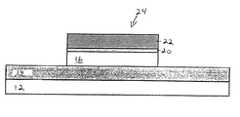
- the initial structure shown in FIG. 1comprises silicon-on-insulating (SOI) material 10 which includes bottom Si-containing layer 12 , insulating region 14 , and top Si-containing layer 16 .
- SOIsilicon-on-insulating
- the insulating regioni.e., buried oxide region, electrically isolates the bottom Si-containing layer from the top Si-containing layer.
- Si-containing layerdenotes a semiconducting material that includes at least Si.
- Such semiconducting materialsinclude, but are not limited to: Si, SiGe, SiGeC, SiC, polysilicon (i.e., polySi), epitaxial silicon (i.e., epi-Si), amorphous silicon (i.e., a:Si), and multilayers thereof.
- layers 12 and 14 of SOI material 10are both composed of Si or polysilicon.
- top Si-containing layer 16 of SOI material 10may vary, but typically, the Si-containing layer has a thickness of from about 10 to about 500 nm, with a thickness of from about 50 to about 150 nm being more highly preferred. Insofar as insulating region 14 is concerned, the insulating region typically has a thickness of from about 10 to about 1000 nm, with a thickness of from about 100 to about 500 nm being more highly preferred.
- the thickness of bottom Si-containing layer 12 of SOI material 10is inconsequential to the present invention.
- the SOI material shown in FIG. 1may be made from a conventional process well known in the art.
- the SOI materialmay be fabricated using a thermal bonding and cutting process, or alternatively, the SOI material is fabricated using a separation by ion implantation of oxygen (SIMOX) process.
- SIMOXseparation by ion implantation of oxygen
- FIG. 2illustrates the structure that is obtained after forming insulating stack 18 atop Si-containing layer 16 .
- insulating stack 18includes at least pad oxide layer 20 which is formed atop Si-containing layer 16 of the SOI material, and polish stop layer which is composed of an insulating layer that has a different etch rate as compared to that of the underlying pad oxide layer.
- the polish stop layermay be composed of a nitride such as SiN, or an oxynitride such as SiON, when the pad oxide is formed of SiO 2 .
- Pad oxide layer 20 of insulating stack 18is formed utilizing a conventional deposition process such as chemical vapor deposition (CVD), plasma-assisted CVD, sputtering, evaporation, chemical solution deposition, or atomic layer deposition.
- CVDchemical vapor deposition
- CVDplasma-assisted CVD
- sputteringevaporation
- chemical solution depositionchemical solution deposition
- atomic layer depositionevaporation
- pad oxide layer 20is formed utilizing a conventional thermal oxidation process.
- the thickness of the pad oxide layermay vary depending on the type of oxide employed as well as the process used in forming the same. Typically, however, pad oxide layer 20 has a thickness of from about 5 to about 200 nm, with a thickness of from about 10 to about 50 nm being more highly preferred.
- the polish stop layerwhich is formed utilizing a conventional deposition process including low-pressure CVD, has a thickness of from about 50 to about 500 nm, with a thickness of from about 100 to about 200 nm being more highly preferred. It is noted that the thickness of the polish stop layer may vary somewhat from the ranges reported herein.
- At least one patterned region 24which is comprised of patterned layers 22 , 20 and 16 , is formed utilizing conventional lithography and etching.
- the lithography step employed in forming the at least one patterned regionincludes the steps of forming a photoresist atop polish stop layer 22 ; exposing the photoresist to a pattern of radiation; and developing the pattern in the photoresist utilizing a conventional resist developer.
- the etching step employed in forming patterned region 24comprises a conventional dry etching process such as reactive-ion etching (RIE), ion beam etching (IBE), plasma etching, laser ablation or any combination thereof which is capable of removing exposed regions of layers 22 , 20 and 16 , while stopping on insulating region 14 .
- RIEreactive-ion etching
- IBEion beam etching
- plasma etchinglaser ablation or any combination thereof which is capable of removing exposed regions of layers 22 , 20 and 16 , while stopping on insulating region 14 .
- patterned resistis removed providing the structure shown in FIG. 3.
- patterned region 24defines the active area, See FIG. 4B, of the inventive structure. It is also noted that although the drawings depict the formation of only one patterned region, the present invention contemplates forming a plurality of such patterned regions on the structure.
- FIGS. 4 A(cross-sectional view)- 4 B (top view)show the structure that is obtained after planarizing isolation regions 26 are formed abutting patterned region 24 .
- the planarizing isolation regionsare formed by first depositing, via conventional deposition processes such as low-pressure CVD, an oxide layer such as SiO 2 over all exposed surfaces of the structure shown in FIG. 3, and thereafter planarizing the deposited oxide layer down to the top surface of polish stop layer 22 utilizing a conventional planarization process such as chemical-mechanical polishing (CMP) or grinding.
- CMPchemical-mechanical polishing
- Patterned hardmask 28is then formed atop the uppermost layer of patterned region 24 , i.e., atop polish stop layer 22 , utilizing a conventional deposition process such as low-pressure CVD, followed by conventional lithography and etching.
- a conventional deposition processsuch as low-pressure CVD, followed by conventional lithography and etching.
- the resultant structure obtained after these steps of the present inventionis shown, for example, in FIG. 5.
- Patterned hardmask 28has a width of about 50 nm or less, with a width of from about 5 to about 50 nm being more highly preferred.
- the vertical thickness of the patterned hardmaskis typically of from about 50 to about 500 nm, with a vertical thickness of from about 100 to about 200 nm being more highly preferred.
- the patterned hardmaskmay be composed of the same or different oxide as planarizing insulating regions 26 and that the patterned hardmask is employed in the present invention in defining channel regions 35 .
- patterned photoresist 30 having at least one opening 32 exposing a portion of patterned hardmask 28is then formed over the structure shown in FIG. 5.
- patterned resist 30 having opening 32is formed utilizing conventional lithography as described hereinabove. It is noted that this step of the present invention defines the regions where the gate conductor will be subsequently formed. At this point of the present invention, any polish stop layer that is adjacent to the channel region, not protected by patterned hardmask 28 , is removed utilizing a selective RIE process.
- FIGS. 6 A- 6 Bthat structure is subjected to selective etching processes that are capable of removing the exposed portions of patterned hardmask 28 as well as the underlying portions of polish stop layer 22 stopping on a portion of pad oxide layer 20 .
- the resulting structure formed after these selective etching processesis shown, for example, in FIGS. 6A (cross-sectional)- 6 B (top view).
- the selective etching processes used at this point of the present inventioninclude the use of a first etching process that selectively removes oxide as compared to nitride, and a second etching process which selectively removes nitride as compared to oxide.
- the first etching processmay comprise the use of a fluorine-containing gas or plasma having an etch selectivity of at least about 20:1, whereas the second etching process may include the use of Cl-based chemistries having an etch selectivity of at least about 10:1. Note that the second etching process defines channel regions 35 of the inventive structure.
- FIGS. 7 A- 7 Bshow the resultant structure after conducting the selective etching processes which provide troughs 34 in the isolation regions for the gate conductors.
- the etchis a fluorine-base chemistry that etches SiO 2 selective to Si 3 N 4 .
- This selective etching processesalso removes the exposed portions of pad oxide 20 from the regions adjacent to the channel (i.e., those regions not protected by hardmask 22 ). See, for example, in FIG. 7B.
- the structure shown in FIG. 8is obtained by utilizing a third selective etching process in which a chlorine-containing etching gas or plasma having an etch selectivity of at least about 10:1; is employed. This etches the exposed Si adjacent to hardmask 22 , leaving a vertical Si FIN that defines the channel regions.
- the resistis removed utilizing a conventional stripping process well known to those skilled in the art. Note that portions of hardmask 28 are also removed at this point of the present invention.
- a sacrificial oxide layer(not shown) is formed by conventional thermal growing processes on the exposed wall portions of the trough, the sacrificial oxide is thereafter removed using a chemical etchant such as HF, and an oxide layer (not shown) is then formed on the exposed, and now cleaned, tough sidewalls.
- a chemical etchantsuch as HF
- FIGS. 9 A(cross-section)- 9 B(top view)show the resultant structure that is obtained after insulating spacers 36 and gate dielectric 38 are formed in the trough.
- the insulating spacersare formed utilizing a conventional deposition process such as low-pressure CVD and etching, e.g., RIE wherein a fluorine-based plasma is employed. Note that over-etching is typically employed so as to remove spacers from the channel regions.
- the thickness of hardmask 22should be greater than the thickness of Si layer 16 so that spacers remain adjacent to the source/drain diffusion regions, but not on the channel regions.
- Insulating spacers 36are comprised of an oxide, a nitride, an oxynitride or any combination and multilayer thereof.
- a sacrificial oxide layer(not shown) is formed, as described above, then the sacrificial oxide layer is removed, as described above, and thereafter gate dielectric 38 is formed by utilizing a conventional deposition process. Alternatively, a conventional thermal growing process may be used in forming the gate dielectric.
- the gate dielectric formed at this point of the present inventionmay include an oxide, a nitride, an oxynitride or any combination thereof including multilayers.
- a preferred gate dielectric employed in the present inventionis an oxynitride such as SiON.
- the thickness of the gate dielectric formed at this point of the present inventionmay vary depending on the gate dielectric material as well as the process used in forming the same.
- gate dielectric 38has an effective electrical thickness assuming the dielectric constant is equal to that of SiO 2 of from about 1 to about 5 nm, with a thickness of from about 1 to about 2 nm being more highly preferred.
- gate conductor 40is formed over the channel and the trough regions shown in FIGS. 9 A- 9 B.
- the resultant structure after formation of gate conductor 40is shown in FIG. 10. Note that the top surface of the gate conductive material is co-planar with the top surface of isolation regions 26 .
- the gate conductor materialis deposited utilizing a conventional deposition process including low-pressure CVD and thereafter a conventional planarization process such as CMP is employed.
- the gate conductor material used at this point of the present inventionincludes any conductive material which is typically employed in MOSFET devices.
- the gate conductive material employed in the present inventionmay be comprised of polysilicon, amorphous Si, elemental metals that are conductive, alloys of conductive elemental metals, silicides or nitrides of conductive elemental metals and multilayers thereof, e.g., a conductive gate stack including, for example, a layer of polysilicon and a conductive elemental metal.
- a conventional diffusion barriersuch as Ta, Ti, TaN or TiN may be formed between the conductive layers.
- Polish stop layer 22 and pad oxide layer 20are then removed from the structure utilizing conventional wet etching processes or a chemical down stream dry etching process well known in the art so as to expose portions of underlying Si-containing layer 16 .
- the exposed portions of the Si-containing layerare then subjecting to a ion implantation process wherein an ion (n- or p-type) is implanted using an ion dose on the order of about 1E15 atoms/cm 2 or greater.
- the doped regions of the Si-containing layerare annealed at a temperature of about 700° C. or greater so as to form activated source/drain diffusion regions 42 that have junction regions which are self-aligned to the gate edges.
- the resultant structure obtained using the inventive processis shown, for example, in FIG. 11A (cross-sectional) and B (top view).
- the inventive structureincludes bottom Si-containing layer 12 , an insulating region ( 14 and 26 ) present atop the bottom Si-containing layer. Insulating region ( 14 + 26 ) having at least one partial opening 50 therein.
- a gate region 70 formed in the partial openingsaid gate region comprising two regions of gate conductor 40 that are separated from channel regions 35 by insulating film, i.e., gate dielectric, 38 which surrounds a portion of Si-containing layer 16 , said insulating film having opposite vertical surfaces adjacent to channel regions 35 ; source/drain diffusion regions 42 abutting said gate region, said source/drain diffusion regions having junctions that are self-aligned to the channels regions as well as the gate region; and insulating spacers 36 that separate gate region 70 and source/drain diffusion regions 42 formed orthogonal to insulating film 38 .
- insulating filmi.e., gate dielectric, 38 which surrounds a portion of Si-containing layer 16 , said insulating film having opposite vertical surfaces adjacent to channel regions 35 ; source/drain diffusion regions 42 abutting said gate region, said source/drain diffusion regions having junctions that are self-aligned to the channels regions as well as the gate region; and insulating spacers 36 that separate gate region 70
- the present inventionalso contemplates other conventional MOSFET processing steps that are well known in the art.
- the present inventionalso contemplates forming salicide regions atop the source/drain diffusion regions, and forming contacts and/or interconnects over the salicide regions.
Landscapes
- Thin Film Transistor (AREA)
Abstract
Description
- The present invention relates to semiconductor devices, and more particularly to a method of forming a metal oxide semiconductor field effect transistor (MOSFET) comprising thin vertical channels (i.e., the FIN) controlled by a double-gate, which involves using a trough to define the channel regions as well as the damascene gate, so as to provide a self-aligned gate. The present invention also relates to a sub-0.05 μm double-gated/double-channel FIN MOSFET structure wherein the gate is self-aligned to the channel regions as well as the source/drain junctions.[0001]
- Over the past twenty-five years or so, the primary challenge of very large scale integration (VLSI) has been the integration of an ever-increasing number of MOSFET devices with high yield and reliability. This was achieved mainly in the prior art by scaling down the MOSFET channel length without excessive short-channel effects. As is known to those skilled in the art, short-channel effects are the decrease of threshold voltage V[0002]tin short-channel devices due to two-dimensional electrostatic charge sharing between the gate and the source/drain diffusion regions.
- To scale down MOSFET channel lengths without excessive short-channel effects, gate oxide thickness has to be reduced while increasing channel-doping concentration. However, Yan, et al., “Scaling the Si MOSFET: From bulk to SOI to bulk”, IEEE Trans. Elect. Dev., Vol. 39, p. 1704, July 1992, have shown that to reduce short-channel effects for sub-0.05 μm MOSFETs, it is important to have a backside-conducting layer present in the structure that screens the drain field away from the channel. The Yan, et al. results show that double-gated MOSFETs and MOSFETs with a top gate and a backside ground plane are more immune to short-channel effects and hence can be scaled to shorter dimensions than conventional MOSFETs.[0003]
- The structure of the prior art MOSFETs consists of a very thin vertical Si layer (FIN) for the channel, with two gates, one on each side of the channel. The two gates are electrically connected so that they serve to modulate the channel. Short-channel effects are greatly suppressed in such a structure because the two gates very effectively terminate the drain field line preventing the drain potential from being felt at the source end of the channel. Consequently, the variation of the threshold voltage with drain voltage and with gate length of a prior art double-gated MOSFET is much smaller than that of a conventional single-gated structure of the same channel length.[0004]
- FIN MOSFETs offer potential benefits in performance as compared with conventional MOSFETs; See, for example, X. Huang, et al., IEDM Tech. Dig. 1999, p.67. However, in prior art FIN MOSFETs, the gate conductor is not self-aligned to the source/drain diffusion junctions or the channel regions. Therefore, there will be a large series resistance between the channel and the heavily doped source/drain diffusion junctions.[0005]
- To date, there are no adequate means for fabricating double-gated FIN MOSFET structures in which the gate is self-aligned to the source/drain diffusion junctions and the channels. Thus, there is a continued need for developing a new and improved method of fabricating double-gated FIN MOSFETs in which such self-alignment between the gate and the source/drain diffusion junctions and channels is achieved.[0006]
- One object of the present invention is to provide a double-gated/double-channel FIN MOSFET structure that has sub-0.05 μm channel lengths associated therewith.[0007]
- Another object of the present invention is to provide a FIN MOSFET structure that has excellent short-channel characteristics.[0008]
- A further object of the present invention is to provide a FIN MOSFET structure in which the variation in threshold voltage with drain voltage and with the gate length is substantially less than that of a singled-gated MOSFET structure of the same channel length.[0009]
- A yet further object of the present invention is to provide a FIN MOSFET structure which has double the on-current as compared with conventional single-gated structures of the same channel length.[0010]
- A still further object of the present invention is to provide a FIN MOSFET structure in which the gate is self-aligned to the source/drain diffusion junctions and channel regions thereby significantly reducing the series resistance between the channels and the heavily doped source/drain diffusion junctions.[0011]
- These and other objects and advantages are achieved in the present invention by utilizing a method wherein a trough is employed, not only to define the regions where the channels are formed, but also to form a damascene gate. Such a method allows for the formation of a double-gated/double-channel FIN MOSFET structure in which the gate is self-aligned to the channel regions and the source/drain diffusion junctions.[0012]
- One aspect of the present invention thus relates to a method of fabricating a double-gated/double-channel FIN MOSFET structure having a gate region that is self-aligned with the source/drain diffusion junctions and channel regions. Specifically, the method of the present invention comprises the steps of:[0013]
- (a) forming at least one patterned region atop a surface of an insulating region, said at least one patterned region comprising a Si-containing layer present atop said insulating region, a pad oxide present atop said Si-containing layer and a polish stop layer present atop said pad oxide;[0014]
- (b) forming planarizing insulating regions abutting each patterned region, said planarizing insulating regions are formed on exposed portions of said insulating region, said planarizing insulating region being co-planar with a top surface of said polish stop layer;[0015]
- (c) forming a hardmask on a portion of said at least one patterned region, said hardmask being used to define channel regions in said at least one patterned region;[0016]
- (d) selectively removing a portion of said hardmask, said polish stop layer and said pad oxide layer so as to expose a portion of said Si-containing layer thereby forming channels regions and a trough;[0017]
- (e) forming a gate region in said trough; and[0018]
- (f) removing said polish stop layer and said pad oxide abutting said gate region so as to expose portions of said Si-containing layer and forming source/drain diffusion regions therein.[0019]
- Another aspect of the present invention relates to a double-gated/double-channel FIN MOSFET structure which is formed utilizing the method of the present invention. Specifically, the inventive double-gated/double-channel FIN MOSFET comprises:[0020]
- a bottom Si-containing layer;[0021]
- an insulating region present atop said bottom Si-containing layer, said insulating region having at least one partial opening therein;[0022]
- a gate region formed in said at least one partial opening, said gate region comprising two regions of gate conductor that are separated from channel regions by an insulating film, said insulating film having opposite vertical surfaces adjacent to the channel regions;[0023]
- source/drain diffusion regions abutting said gate region, said source/drain diffusion regions having junctions that are self-aligned to the channels regions as well as the gate region; and[0024]
- insulating spacers that separate the gate region and the source/drain diffusion regions formed orthogonal to said insulating film.[0025]
- FIGS.[0026]1-11 are pictorial representations (through cross-sectional and, in some instances, top views) showing the inventive double-gated/double-channel FIN MOSFET structure through various processing steps of the present invention.
- The present invention, which provides a method of fabricating a FIN MOSFET structure having a gate region that is self-aligned with the source/drain diffusion junctions and channel regions as well as the FIN MOSFET structure itself, will now be described in greater detail by referring to the drawings that accompany the present application. It is noted that in the accompanying drawings, like and/or corresponding elements are referred to by like reference numerals.[0027]
- Reference is first made to FIG. 1 which illustrates an initial structure that is employed in the present invention in fabricating the inventive FIN MOSFET structure. Specifically, the initial structure shown in FIG. 1 comprises silicon-on-insulating (SOI)[0028]
material 10 which includes bottom Si-containinglayer 12,insulating region 14, and top Si-containinglayer 16. Note that the insulating region, i.e., buried oxide region, electrically isolates the bottom Si-containing layer from the top Si-containing layer. The term “Si-containing layer” as used herein denotes a semiconducting material that includes at least Si. Examples of such semiconducting materials, include, but are not limited to: Si, SiGe, SiGeC, SiC, polysilicon (i.e., polySi), epitaxial silicon (i.e., epi-Si), amorphous silicon (i.e., a:Si), and multilayers thereof. In one embodiment of the present invention, it is highly preferred thatlayers SOI material 10 are both composed of Si or polysilicon. - The thickness of top Si-containing[0029]
layer 16 ofSOI material 10 may vary, but typically, the Si-containing layer has a thickness of from about 10 to about 500 nm, with a thickness of from about 50 to about 150 nm being more highly preferred. Insofar asinsulating region 14 is concerned, the insulating region typically has a thickness of from about 10 to about 1000 nm, with a thickness of from about 100 to about 500 nm being more highly preferred. The thickness of bottom Si-containinglayer 12 ofSOI material 10 is inconsequential to the present invention. - The SOI material shown in FIG. 1 may be made from a conventional process well known in the art. For example, the SOI material may be fabricated using a thermal bonding and cutting process, or alternatively, the SOI material is fabricated using a separation by ion implantation of oxygen (SIMOX) process.[0030]
- FIG. 2 illustrates the structure that is obtained after forming[0031]
insulating stack 18 atop Si-containinglayer 16. As shown,insulating stack 18 includes at leastpad oxide layer 20 which is formed atop Si-containinglayer 16 of the SOI material, and polish stop layer which is composed of an insulating layer that has a different etch rate as compared to that of the underlying pad oxide layer. For example, the polish stop layer may be composed of a nitride such as SiN, or an oxynitride such as SiON, when the pad oxide is formed of SiO2.Pad oxide layer 20 of insulatingstack 18 is formed utilizing a conventional deposition process such as chemical vapor deposition (CVD), plasma-assisted CVD, sputtering, evaporation, chemical solution deposition, or atomic layer deposition. Alternatively, and more preferably,pad oxide layer 20 is formed utilizing a conventional thermal oxidation process. The thickness of the pad oxide layer may vary depending on the type of oxide employed as well as the process used in forming the same. Typically, however,pad oxide layer 20 has a thickness of from about 5 to about 200 nm, with a thickness of from about 10 to about 50 nm being more highly preferred. - The polish stop layer, which is formed utilizing a conventional deposition process including low-pressure CVD, has a thickness of from about 50 to about 500 nm, with a thickness of from about 100 to about 200 nm being more highly preferred. It is noted that the thickness of the polish stop layer may vary somewhat from the ranges reported herein.[0032]
- Next, and as shown in FIG. 3, at least one patterned[0033]
region 24, which is comprised of patternedlayers polish stop layer 22; exposing the photoresist to a pattern of radiation; and developing the pattern in the photoresist utilizing a conventional resist developer. The etching step employed in forming patternedregion 24 comprises a conventional dry etching process such as reactive-ion etching (RIE), ion beam etching (IBE), plasma etching, laser ablation or any combination thereof which is capable of removing exposed regions oflayers region 14. - Following the etching process, the patterned resist is removed providing the structure shown in FIG. 3. Note that patterned[0034]
region 24 defines the active area, See FIG. 4B, of the inventive structure. It is also noted that although the drawings depict the formation of only one patterned region, the present invention contemplates forming a plurality of such patterned regions on the structure. - FIGS.[0035]4A(cross-sectional view)-4B (top view) show the structure that is obtained after planarizing
isolation regions 26 are formed abutting patternedregion 24. The planarizing isolation regions are formed by first depositing, via conventional deposition processes such as low-pressure CVD, an oxide layer such as SiO2over all exposed surfaces of the structure shown in FIG. 3, and thereafter planarizing the deposited oxide layer down to the top surface ofpolish stop layer 22 utilizing a conventional planarization process such as chemical-mechanical polishing (CMP) or grinding. - Patterned[0036]
hardmask 28 is then formed atop the uppermost layer of patternedregion 24, i.e., atoppolish stop layer 22, utilizing a conventional deposition process such as low-pressure CVD, followed by conventional lithography and etching. The resultant structure obtained after these steps of the present invention is shown, for example, in FIG. 5. - Patterned[0037]
hardmask 28 has a width of about 50 nm or less, with a width of from about 5 to about 50 nm being more highly preferred. The vertical thickness of the patterned hardmask is typically of from about 50 to about 500 nm, with a vertical thickness of from about 100 to about 200 nm being more highly preferred. Note that the patterned hardmask may be composed of the same or different oxide as planarizing insulatingregions 26 and that the patterned hardmask is employed in the present invention in definingchannel regions 35. - Next, and as illustrated in FIGS. 6A (cross-sectional)-[0038]6B (top view), patterned
photoresist 30 having at least oneopening 32 exposing a portion of patternedhardmask 28 is then formed over the structure shown in FIG. 5. Specifically, patterned resist30 havingopening 32 is formed utilizing conventional lithography as described hereinabove. It is noted that this step of the present invention defines the regions where the gate conductor will be subsequently formed. At this point of the present invention, any polish stop layer that is adjacent to the channel region, not protected by patternedhardmask 28, is removed utilizing a selective RIE process. - To define the structure shown in FIGS.[0039]6A-6B, that structure is subjected to selective etching processes that are capable of removing the exposed portions of patterned
hardmask 28 as well as the underlying portions ofpolish stop layer 22 stopping on a portion ofpad oxide layer 20. The resulting structure formed after these selective etching processes is shown, for example, in FIGS. 6A (cross-sectional)-6B (top view). The selective etching processes used at this point of the present invention include the use of a first etching process that selectively removes oxide as compared to nitride, and a second etching process which selectively removes nitride as compared to oxide. - The first etching process may comprise the use of a fluorine-containing gas or plasma having an etch selectivity of at least about 20:1, whereas the second etching process may include the use of Cl-based chemistries having an etch selectivity of at least about 10:1. Note that the second etching process defines[0040]
channel regions 35 of the inventive structure. - FIGS.[0041]7A-7B show the resultant structure after conducting the selective etching processes which provide
troughs 34 in the isolation regions for the gate conductors. The etch is a fluorine-base chemistry that etches SiO2selective to Si3N4. - This selective etching processes also removes the exposed portions of[0042]
pad oxide 20 from the regions adjacent to the channel (i.e., those regions not protected by hardmask22). See, for example, in FIG. 7B. The structure shown in FIG. 8 is obtained by utilizing a third selective etching process in which a chlorine-containing etching gas or plasma having an etch selectivity of at least about 10:1; is employed. This etches the exposed Si adjacent to hardmask22, leaving a vertical Si FIN that defines the channel regions. Following the third selective etching process, the resist is removed utilizing a conventional stripping process well known to those skilled in the art. Note that portions ofhardmask 28 are also removed at this point of the present invention. - After stripping the resist from the structure, a sacrificial oxide layer (not shown) is formed by conventional thermal growing processes on the exposed wall portions of the trough, the sacrificial oxide is thereafter removed using a chemical etchant such as HF, and an oxide layer (not shown) is then formed on the exposed, and now cleaned, tough sidewalls.[0043]
- FIGS.[0044]9A(cross-section)-9B(top view) show the resultant structure that is obtained after insulating
spacers 36 andgate dielectric 38 are formed in the trough. Specifically, the insulating spacers are formed utilizing a conventional deposition process such as low-pressure CVD and etching, e.g., RIE wherein a fluorine-based plasma is employed. Note that over-etching is typically employed so as to remove spacers from the channel regions. The thickness ofhardmask 22 should be greater than the thickness ofSi layer 16 so that spacers remain adjacent to the source/drain diffusion regions, but not on the channel regions. Insulatingspacers 36 are comprised of an oxide, a nitride, an oxynitride or any combination and multilayer thereof. - Next, a sacrificial oxide layer (not shown) is formed, as described above, then the sacrificial oxide layer is removed, as described above, and thereafter[0045]
gate dielectric 38 is formed by utilizing a conventional deposition process. Alternatively, a conventional thermal growing process may be used in forming the gate dielectric. - The gate dielectric formed at this point of the present invention may include an oxide, a nitride, an oxynitride or any combination thereof including multilayers. A preferred gate dielectric employed in the present invention is an oxynitride such as SiON.[0046]
- The thickness of the gate dielectric formed at this point of the present invention may vary depending on the gate dielectric material as well as the process used in forming the same. Typically,[0047]
gate dielectric 38 has an effective electrical thickness assuming the dielectric constant is equal to that of SiO2of from about 1 to about 5 nm, with a thickness of from about 1 to about 2 nm being more highly preferred. - Following the formation of the insulating spacers and gate dielectric,[0048]
gate conductor 40 is formed over the channel and the trough regions shown in FIGS.9A-9B. The resultant structure after formation ofgate conductor 40 is shown in FIG. 10. Note that the top surface of the gate conductive material is co-planar with the top surface ofisolation regions 26. Specifically, the gate conductor material is deposited utilizing a conventional deposition process including low-pressure CVD and thereafter a conventional planarization process such as CMP is employed. - The gate conductor material used at this point of the present invention includes any conductive material which is typically employed in MOSFET devices. For example, the gate conductive material employed in the present invention may be comprised of polysilicon, amorphous Si, elemental metals that are conductive, alloys of conductive elemental metals, silicides or nitrides of conductive elemental metals and multilayers thereof, e.g., a conductive gate stack including, for example, a layer of polysilicon and a conductive elemental metal. When a conductive gate stack is employed, a conventional diffusion barrier such as Ta, Ti, TaN or TiN may be formed between the conductive layers.[0049]
- [0050]
Polish stop layer 22 andpad oxide layer 20 are then removed from the structure utilizing conventional wet etching processes or a chemical down stream dry etching process well known in the art so as to expose portions of underlying Si-containinglayer 16. The exposed portions of the Si-containing layer are then subjecting to a ion implantation process wherein an ion (n- or p-type) is implanted using an ion dose on the order of about 1E15 atoms/cm2or greater. Following ion implantation, the doped regions of the Si-containing layer are annealed at a temperature of about 700° C. or greater so as to form activated source/drain diffusion regions 42 that have junction regions which are self-aligned to the gate edges. - The resultant structure obtained using the inventive process is shown, for example, in FIG. 11A (cross-sectional) and B (top view). Specifically, the inventive structure includes bottom Si-containing[0051]
layer 12, an insulating region (14 and26) present atop the bottom Si-containing layer. Insulating region (14+26) having at least onepartial opening 50 therein. Agate region 70 formed in the partial opening, said gate region comprising two regions ofgate conductor 40 that are separated fromchannel regions 35 by insulating film, i.e., gate dielectric,38 which surrounds a portion of Si-containinglayer 16, said insulating film having opposite vertical surfaces adjacent to channelregions 35; source/drain diffusion regions 42 abutting said gate region, said source/drain diffusion regions having junctions that are self-aligned to the channels regions as well as the gate region; and insulatingspacers 36 that separategate region 70 and source/drain diffusion regions 42 formed orthogonal to insulatingfilm 38. - In addition to the processing steps mentioned above, the present invention also contemplates other conventional MOSFET processing steps that are well known in the art. For example, the present invention also contemplates forming salicide regions atop the source/drain diffusion regions, and forming contacts and/or interconnects over the salicide regions.[0052]
- While the present invention has been particularly shown and described with respect to preferred embodiments thereof, it will be understood by those skilled in the art that the foregoing and other changes in forms and details may be made without departing from the scope and spirit of the present invention. It is therefore intended that the present invention not be limited to the exact forms and details described and illustrated, but fall within the scope of the appended claims.[0053]
Claims (20)
Priority Applications (2)
| Application Number | Priority Date | Filing Date | Title |
|---|---|---|---|
| US09/965,288US6689650B2 (en) | 2001-09-27 | 2001-09-27 | Fin field effect transistor with self-aligned gate |
| US10/695,335US7173303B2 (en) | 2001-09-27 | 2003-10-28 | FIN field effect transistor with self-aligned gate |
Applications Claiming Priority (1)
| Application Number | Priority Date | Filing Date | Title |
|---|---|---|---|
| US09/965,288US6689650B2 (en) | 2001-09-27 | 2001-09-27 | Fin field effect transistor with self-aligned gate |
Related Child Applications (1)
| Application Number | Title | Priority Date | Filing Date |
|---|---|---|---|
| US10/695,335DivisionUS7173303B2 (en) | 2001-09-27 | 2003-10-28 | FIN field effect transistor with self-aligned gate |
Publications (2)
| Publication Number | Publication Date |
|---|---|
| US20030057486A1true US20030057486A1 (en) | 2003-03-27 |
| US6689650B2 US6689650B2 (en) | 2004-02-10 |
Family
ID=25509749
Family Applications (2)
| Application Number | Title | Priority Date | Filing Date |
|---|---|---|---|
| US09/965,288Expired - LifetimeUS6689650B2 (en) | 2001-09-27 | 2001-09-27 | Fin field effect transistor with self-aligned gate |
| US10/695,335Expired - LifetimeUS7173303B2 (en) | 2001-09-27 | 2003-10-28 | FIN field effect transistor with self-aligned gate |
Family Applications After (1)
| Application Number | Title | Priority Date | Filing Date |
|---|---|---|---|
| US10/695,335Expired - LifetimeUS7173303B2 (en) | 2001-09-27 | 2003-10-28 | FIN field effect transistor with self-aligned gate |
Country Status (1)
| Country | Link |
|---|---|
| US (2) | US6689650B2 (en) |
Cited By (72)
| Publication number | Priority date | Publication date | Assignee | Title |
|---|---|---|---|---|
| US20030235989A1 (en)* | 2002-06-25 | 2003-12-25 | Seagate Technology Llc | Process for CMP assisted liftoff |
| US20040036126A1 (en)* | 2002-08-23 | 2004-02-26 | Chau Robert S. | Tri-gate devices and methods of fabrication |
| US20040227187A1 (en)* | 2003-02-13 | 2004-11-18 | Zhiyuan Cheng | Integrated semiconductor device and method to make same |
| WO2004112146A1 (en)* | 2003-06-12 | 2004-12-23 | Advanced Micro Devices, Inc. | Finfet with dual silicon gate layer for chemical mechanical polishing planarization |
| US20050003593A1 (en)* | 2003-06-23 | 2005-01-06 | Advanced Micro Devices, Inc. | Semiconductor device and method of manufacture |
| US20050121706A1 (en)* | 2003-02-20 | 2005-06-09 | Hao-Yu Chen | Semiconductor nano-rod devices |
| US20050148137A1 (en)* | 2003-12-30 | 2005-07-07 | Brask Justin K. | Nonplanar transistors with metal gate electrodes |
| US20050158970A1 (en)* | 2004-01-16 | 2005-07-21 | Robert Chau | Tri-gate transistors and methods to fabricate same |
| US20050218438A1 (en)* | 2004-03-31 | 2005-10-06 | Nick Lindert | Bulk non-planar transistor having strained enhanced mobility and methods of fabrication |
| US20050242406A1 (en)* | 2003-06-27 | 2005-11-03 | Hareland Scott A | Nonplanar device with stress incorporation layer and method of fabrication |
| US6969659B1 (en) | 2004-08-12 | 2005-11-29 | International Business Machines Corporation | FinFETs (Fin Field Effect Transistors) |
| US20050266692A1 (en)* | 2004-06-01 | 2005-12-01 | Brask Justin K | Method of patterning a film |
| US20050275010A1 (en)* | 2004-06-10 | 2005-12-15 | Hung-Wei Chen | Semiconductor nano-wire devices and methods of fabrication |
| US20060033095A1 (en)* | 2004-08-10 | 2006-02-16 | Doyle Brian S | Non-planar pMOS structure with a strained channel region and an integrated strained CMOS flow |
| US20060063332A1 (en)* | 2004-09-23 | 2006-03-23 | Brian Doyle | U-gate transistors and methods of fabrication |
| US20060071275A1 (en)* | 2004-09-30 | 2006-04-06 | Brask Justin K | Nonplanar transistors with metal gate electrodes |
| US20060086977A1 (en)* | 2004-10-25 | 2006-04-27 | Uday Shah | Nonplanar device with thinned lower body portion and method of fabrication |
| US20060091428A1 (en)* | 2003-06-27 | 2006-05-04 | Yee-Chia Yeo | Structure and method for forming the gate electrode in a multiple-gate transistor |
| KR100578745B1 (en)* | 2003-12-26 | 2006-05-12 | 한국전자통신연구원 | Multi-gate MOS transistor and a method for manufacturing the same |
| US20060128131A1 (en)* | 2004-09-29 | 2006-06-15 | Chang Peter L | Independently accessed double-gate and tri-gate transistors in same process flow |
| US20060157794A1 (en)* | 2005-01-18 | 2006-07-20 | Doyle Brian S | Non-planar MOS structure with a strained channel region |
| US20060172497A1 (en)* | 2003-06-27 | 2006-08-03 | Hareland Scott A | Nonplanar semiconductor device with partially or fully wrapped around gate electrode and methods of fabrication |
| US20060186484A1 (en)* | 2005-02-23 | 2006-08-24 | Chau Robert S | Field effect transistor with narrow bandgap source and drain regions and method of fabrication |
| US20060189043A1 (en)* | 2005-02-18 | 2006-08-24 | Thomas Schulz | Trench-gate electrode for FinFET device |
| US20060202266A1 (en)* | 2005-03-14 | 2006-09-14 | Marko Radosavljevic | Field effect transistor with metal source/drain regions |
| US20060220133A1 (en)* | 2003-04-29 | 2006-10-05 | Yee-Chia Yeo | Doping of semiconductor fin devices |
| US20060223302A1 (en)* | 2005-03-31 | 2006-10-05 | Chang Peter L | Self-aligned contacts for transistors |
| US20060286755A1 (en)* | 2005-06-15 | 2006-12-21 | Brask Justin K | Method for fabricating transistor with thinned channel |
| US20070001219A1 (en)* | 2005-06-30 | 2007-01-04 | Marko Radosavljevic | Block contact architectures for nanoscale channel transistors |
| US20070001173A1 (en)* | 2005-06-21 | 2007-01-04 | Brask Justin K | Semiconductor device structures and methods of forming semiconductor structures |
| US20070040223A1 (en)* | 2005-08-17 | 2007-02-22 | Intel Corporation | Lateral undercut of metal gate in SOI device |
| US20070090408A1 (en)* | 2005-09-29 | 2007-04-26 | Amlan Majumdar | Narrow-body multiple-gate FET with dominant body transistor for high performance |
| US20070090416A1 (en)* | 2005-09-28 | 2007-04-26 | Doyle Brian S | CMOS devices with a single work function gate electrode and method of fabrication |
| US20070148837A1 (en)* | 2005-12-27 | 2007-06-28 | Uday Shah | Method of fabricating a multi-cornered film |
| US20070152266A1 (en)* | 2005-12-29 | 2007-07-05 | Intel Corporation | Method and structure for reducing the external resistance of a three-dimensional transistor through use of epitaxial layers |
| US20070158679A1 (en)* | 2005-12-31 | 2007-07-12 | Samsung Electronics Co., Ltd. | Semiconductor device with multiple channels and method of fabricating the same |
| US20070238273A1 (en)* | 2006-03-31 | 2007-10-11 | Doyle Brian S | Method of ion implanting for tri-gate devices |
| US20080001236A1 (en)* | 2006-06-28 | 2008-01-03 | Change Peter L D | Method of forming a transistor having gate protection and transistor formed according to the method |
| CN100369208C (en)* | 2004-04-16 | 2008-02-13 | 台湾积体电路制造股份有限公司 | Method of forming gate electrode on multi-gate transistor of semiconductor device |
| US20080093622A1 (en)* | 2006-10-19 | 2008-04-24 | Amberwave Systems Corporation | Light-Emitter-Based Devices with Lattice-Mismatched Semiconductor Structures |
| US20080099839A1 (en)* | 2006-06-14 | 2008-05-01 | Willy Rachmady | Ultra-thin oxide bonding for S1 to S1 dual orientation bonding |
| US20080157225A1 (en)* | 2006-12-29 | 2008-07-03 | Suman Datta | SRAM and logic transistors with variable height multi-gate transistor architecture |
| US20080257409A1 (en)* | 2007-04-09 | 2008-10-23 | Amberwave Systems Corporation | Photovoltaics on silicon |
| US7479421B2 (en) | 2005-09-28 | 2009-01-20 | Intel Corporation | Process for integrating planar and non-planar CMOS transistors on a bulk substrate and article made thereby |
| CN100466186C (en)* | 2003-05-22 | 2009-03-04 | 飞思卡尔半导体公司 | Method for fabricating transistor with independent gate structure |
| US20090065047A1 (en)* | 2007-09-07 | 2009-03-12 | Amberwave Systems Corporation | Multi-Junction Solar Cells |
| US20090149531A1 (en)* | 2007-12-11 | 2009-06-11 | Apoteknos Para La Piel, S.L. | Chemical composition derived from p-hydroxyphenyl propionic acid for the treatment of psoriasis |
| US20100072515A1 (en)* | 2008-09-19 | 2010-03-25 | Amberwave Systems Corporation | Fabrication and structures of crystalline material |
| US20100078680A1 (en)* | 2008-09-24 | 2010-04-01 | Amberwave Systems Corporation | Semiconductor sensor structures with reduced dislocation defect densities and related methods for the same |
| US20100176375A1 (en)* | 2009-01-09 | 2010-07-15 | Taiwan Semiconductor Manufacturing Company, Ltd. | Diode-Based Devices and Methods for Making the Same |
| US20100176371A1 (en)* | 2009-01-09 | 2010-07-15 | Taiwan Semiconductor Manufacturing Company, Ltd. | Semiconductor Diodes Fabricated by Aspect Ratio Trapping with Coalesced Films |
| US20100213511A1 (en)* | 2006-03-24 | 2010-08-26 | Taiwan Semiconductor Manufacturing Company, Ltd. | Lattice-Mismatched Semiconductor Structures and Related Methods for Device Fabrication |
| US20100252861A1 (en)* | 2009-04-02 | 2010-10-07 | Taiwan Semiconductor Manufacturing Company, Ltd. | Devices Formed from a Non-Polar Plane of a Crystalline Material and Method of Making the Same |
| US20110011438A1 (en)* | 2007-04-09 | 2011-01-20 | Taiwan Semiconductor Manufacturing Company, Ltd. | Nitride-Based Multi-Junction Solar Cell Modules and Methods for Making the Same |
| US20110086498A1 (en)* | 2006-09-27 | 2011-04-14 | Taiwan Semiconductor Manufacturing Company, Ltd. | Quantum Tunneling Devices and Circuits with Lattice-Mismatched Semiconductor Structures |
| US20110156145A1 (en)* | 2004-09-29 | 2011-06-30 | Marko Radosavljevic | Fabrication of channel wraparound gate structure for field-effect transistor |
| US7989280B2 (en) | 2005-11-30 | 2011-08-02 | Intel Corporation | Dielectric interface for group III-V semiconductor device |
| US8084818B2 (en) | 2004-06-30 | 2011-12-27 | Intel Corporation | High mobility tri-gate devices and methods of fabrication |
| US8274097B2 (en) | 2008-07-01 | 2012-09-25 | Taiwan Semiconductor Manufacturing Company, Ltd. | Reduction of edge effects from aspect ratio trapping |
| US8324660B2 (en) | 2005-05-17 | 2012-12-04 | Taiwan Semiconductor Manufacturing Company, Ltd. | Lattice-mismatched semiconductor structures with reduced dislocation defect densities and related methods for device fabrication |
| US8329541B2 (en) | 2007-06-15 | 2012-12-11 | Taiwan Semiconductor Manufacturing Company, Ltd. | InP-based transistor fabrication |
| US8362566B2 (en) | 2008-06-23 | 2013-01-29 | Intel Corporation | Stress in trigate devices using complimentary gate fill materials |
| US8384196B2 (en) | 2008-09-19 | 2013-02-26 | Taiwan Semiconductor Manufacturing Company, Ltd. | Formation of devices by epitaxial layer overgrowth |
| US8557648B2 (en) | 2012-01-11 | 2013-10-15 | International Business Machines Corporation | Recessed source and drain regions for FinFETs |
| US8617945B2 (en) | 2006-08-02 | 2013-12-31 | Intel Corporation | Stacking fault and twin blocking barrier for integrating III-V on Si |
| US8822248B2 (en) | 2008-06-03 | 2014-09-02 | Taiwan Semiconductor Manufacturing Company, Ltd. | Epitaxial growth of crystalline material |
| US8847279B2 (en) | 2006-09-07 | 2014-09-30 | Taiwan Semiconductor Manufacturing Company, Ltd. | Defect reduction using aspect ratio trapping |
| US8981427B2 (en) | 2008-07-15 | 2015-03-17 | Taiwan Semiconductor Manufacturing Company, Ltd. | Polishing of small composite semiconductor materials |
| US9059043B1 (en)* | 2014-02-11 | 2015-06-16 | International Business Machines Corporation | Fin field effect transistor with self-aligned source/drain regions |
| US9859381B2 (en) | 2005-05-17 | 2018-01-02 | Taiwan Semiconductor Manufacturing Company, Ltd. | Lattice-mismatched semiconductor structures with reduced dislocation defect densities and related methods for device fabrication |
| US10304940B1 (en)* | 2017-11-30 | 2019-05-28 | Intel Corporation | Gate cut and fin trim isolation for advanced integrated circuit structure fabrication |
| US11322601B2 (en) | 2017-11-30 | 2022-05-03 | Intel Corporation | Gate cut and fin trim isolation for advanced integrated circuit structure fabrication |
Families Citing this family (67)
| Publication number | Priority date | Publication date | Assignee | Title |
|---|---|---|---|---|
| US6982460B1 (en)* | 2000-07-07 | 2006-01-03 | International Business Machines Corporation | Self-aligned gate MOSFET with separate gates |
| US6657259B2 (en)* | 2001-12-04 | 2003-12-02 | International Business Machines Corporation | Multiple-plane FinFET CMOS |
| US20030151077A1 (en)* | 2002-02-13 | 2003-08-14 | Leo Mathew | Method of forming a vertical double gate semiconductor device and structure thereof |
| US6974729B2 (en)* | 2002-07-16 | 2005-12-13 | Interuniversitair Microelektronica Centrum (Imec) | Integrated semiconductor fin device and a method for manufacturing such device |
| US6888219B2 (en)* | 2002-08-29 | 2005-05-03 | Honeywell International, Inc. | Integrated structure with microwave components |
| KR100481209B1 (en)* | 2002-10-01 | 2005-04-08 | 삼성전자주식회사 | MOS Transistor having multiple channels and method of manufacturing the same |
| US6611029B1 (en)* | 2002-11-08 | 2003-08-26 | Advanced Micro Devices, Inc. | Double gate semiconductor device having separate gates |
| US6709982B1 (en)* | 2002-11-26 | 2004-03-23 | Advanced Micro Devices, Inc. | Double spacer FinFET formation |
| US7148526B1 (en) | 2003-01-23 | 2006-12-12 | Advanced Micro Devices, Inc. | Germanium MOSFET devices and methods for making same |
| US6967143B2 (en)* | 2003-04-30 | 2005-11-22 | Freescale Semiconductor, Inc. | Semiconductor fabrication process with asymmetrical conductive spacers |
| US6838322B2 (en)* | 2003-05-01 | 2005-01-04 | Freescale Semiconductor, Inc. | Method for forming a double-gated semiconductor device |
| US6903967B2 (en)* | 2003-05-22 | 2005-06-07 | Freescale Semiconductor, Inc. | Memory with charge storage locations and adjacent gate structures |
| US7045401B2 (en)* | 2003-06-23 | 2006-05-16 | Sharp Laboratories Of America, Inc. | Strained silicon finFET device |
| KR100517559B1 (en)* | 2003-06-27 | 2005-09-28 | 삼성전자주식회사 | Fin field effect transistor and method for forming of fin therein |
| KR100543207B1 (en)* | 2003-06-30 | 2006-01-20 | 주식회사 하이닉스반도체 | Method for manufacturing gate electrode of semiconductor device using hard mask |
| US6716686B1 (en) | 2003-07-08 | 2004-04-06 | Advanced Micro Devices, Inc. | Method for forming channels in a finfet device |
| US7078299B2 (en)* | 2003-09-03 | 2006-07-18 | Advanced Micro Devices, Inc. | Formation of finFET using a sidewall epitaxial layer |
| US6970373B2 (en)* | 2003-10-02 | 2005-11-29 | Intel Corporation | Method and apparatus for improving stability of a 6T CMOS SRAM cell |
| US7098502B2 (en)* | 2003-11-10 | 2006-08-29 | Freescale Semiconductor, Inc. | Transistor having three electrically isolated electrodes and method of formation |
| US7498225B1 (en) | 2003-12-04 | 2009-03-03 | Advanced Micro Devices, Inc. | Systems and methods for forming multiple fin structures using metal-induced-crystallization |
| WO2005064682A1 (en)* | 2003-12-08 | 2005-07-14 | International Business Machines Corporation | Semiconductor memory device with increased node capacitance |
| US7335945B2 (en)* | 2003-12-26 | 2008-02-26 | Electronics And Telecommunications Research Institute | Multi-gate MOS transistor and method of manufacturing the same |
| US8217450B1 (en) | 2004-02-03 | 2012-07-10 | GlobalFoundries, Inc. | Double-gate semiconductor device with gate contacts formed adjacent sidewalls of a fin |
| KR100574971B1 (en)* | 2004-02-17 | 2006-05-02 | 삼성전자주식회사 | Multi-gate structure semiconductor device and manufacturing method thereof |
| KR100549008B1 (en)* | 2004-03-17 | 2006-02-02 | 삼성전자주식회사 | How to manufacture a fin field effect transistor using isotropic etching technology |
| KR100576361B1 (en)* | 2004-03-23 | 2006-05-03 | 삼성전자주식회사 | 3D CMOS field effect transistor and method of manufacturing the same |
| US7084018B1 (en)* | 2004-05-05 | 2006-08-01 | Advanced Micro Devices, Inc. | Sacrificial oxide for minimizing box undercut in damascene FinFET |
| US7112997B1 (en) | 2004-05-19 | 2006-09-26 | Altera Corporation | Apparatus and methods for multi-gate silicon-on-insulator transistors |
| TW200629427A (en)* | 2004-11-10 | 2006-08-16 | Gil Asa | Transistor structure and method of manufacturing thereof |
| US7472576B1 (en) | 2004-11-17 | 2009-01-06 | State Of Oregon Acting By And Through The State Board Of Higher Education On Behalf Of Portland State University | Nanometrology device standards for scanning probe microscopes and processes for their fabrication and use |
| TWI295506B (en) | 2005-02-03 | 2008-04-01 | Samsung Electronics Co Ltd | Semiconductor device having transistor with vertical gate electrode and method of fabricating the same |
| US20060197140A1 (en)* | 2005-03-04 | 2006-09-07 | Freescale Semiconductor, Inc. | Vertical transistor NVM with body contact structure and method |
| KR100618900B1 (en)* | 2005-06-13 | 2006-09-01 | 삼성전자주식회사 | Method for manufacturing a MOS field effect transistor having a multi-channel and a MOS field effect transistor having a multi-channel manufactured according to the |
| US7309626B2 (en)* | 2005-11-15 | 2007-12-18 | International Business Machines Corporation | Quasi self-aligned source/drain FinFET process |
| US7402856B2 (en)* | 2005-12-09 | 2008-07-22 | Intel Corporation | Non-planar microelectronic device having isolation element to mitigate fringe effects and method to fabricate same |
| US7439588B2 (en)* | 2005-12-13 | 2008-10-21 | Intel Corporation | Tri-gate integration with embedded floating body memory cell using a high-K dual metal gate |
| US7512017B2 (en)* | 2005-12-21 | 2009-03-31 | Intel Corporation | Integration of planar and tri-gate devices on the same substrate |
| US7525160B2 (en) | 2005-12-27 | 2009-04-28 | Intel Corporation | Multigate device with recessed strain regions |
| US20070148926A1 (en)* | 2005-12-28 | 2007-06-28 | Intel Corporation | Dual halo implant for improving short channel effect in three-dimensional tri-gate transistors |
| FR2895835B1 (en)* | 2005-12-30 | 2008-05-09 | Commissariat Energie Atomique | ACHIEVING A MULTI-BRANCH CHANNEL STRUCTURE OF A TRANSISTOR GRID AND MEANS FOR ISOLATING THIS GRID FROM THE SOURCE AND DRAIN REGIONS |
| US7432122B2 (en) | 2006-01-06 | 2008-10-07 | Freescale Semiconductor, Inc. | Electronic device and a process for forming the electronic device |
| CN101017783B (en)* | 2006-02-06 | 2013-06-19 | 中芯国际集成电路制造(上海)有限公司 | Method for making the separated dual-bar field effect transistor |
| CN101017848B (en)* | 2006-02-06 | 2010-08-11 | 中芯国际集成电路制造(上海)有限公司 | Separated dual bar field effect transistor |
| US7473946B2 (en)* | 2006-02-22 | 2009-01-06 | International Business Machines Corporation | CMOS structure and method including multiple crystallographic planes |
| US20070235763A1 (en)* | 2006-03-29 | 2007-10-11 | Doyle Brian S | Substrate band gap engineered multi-gate pMOS devices |
| US7425500B2 (en)* | 2006-03-31 | 2008-09-16 | Intel Corporation | Uniform silicide metal on epitaxially grown source and drain regions of three-dimensional transistors |
| US7407847B2 (en)* | 2006-03-31 | 2008-08-05 | Intel Corporation | Stacked multi-gate transistor design and method of fabrication |
| KR101146588B1 (en)* | 2006-08-11 | 2012-05-16 | 삼성전자주식회사 | Manufacturing method of fin structure and fin transistor adopting the fin structure |
| US7435683B2 (en)* | 2006-09-15 | 2008-10-14 | Intel Corporation | Apparatus and method for selectively recessing spacers on multi-gate devices |
| US20080097346A1 (en)* | 2006-09-19 | 2008-04-24 | Alcon, Inc. | Trocar cannula |
| US7700470B2 (en) | 2006-09-22 | 2010-04-20 | Intel Corporation | Selective anisotropic wet etching of workfunction metal for semiconductor devices |
| FR2921757B1 (en)* | 2007-09-28 | 2009-12-18 | Commissariat Energie Atomique | DOUBLE-GRID TRANSISTOR STRUCTURE WITH MULTI-BRANCH CHANNEL |
| US7927938B2 (en)* | 2007-11-19 | 2011-04-19 | Micron Technology, Inc. | Fin-JFET |
| US20100155801A1 (en)* | 2008-12-22 | 2010-06-24 | Doyle Brian S | Integrated circuit, 1T-1C embedded memory cell containing same, and method of manufacturing 1T-1C memory cell for embedded memory application |
| US7999298B2 (en)* | 2008-12-30 | 2011-08-16 | Intel Corporation | Embedded memory cell and method of manufacturing same |
| US9257325B2 (en)* | 2009-09-18 | 2016-02-09 | GlobalFoundries, Inc. | Semiconductor structures and methods for forming isolation between Fin structures of FinFET devices |
| KR101056229B1 (en) | 2009-10-12 | 2011-08-11 | 삼성모바일디스플레이주식회사 | An organic light emitting display device comprising a thin film transistor, a method of manufacturing the same, and a thin film transistor |
| US8563376B2 (en) | 2011-12-16 | 2013-10-22 | International Business Machines Corporation | Hybrid CMOS nanowire mesh device and bulk CMOS device |
| US8709888B2 (en) | 2011-12-16 | 2014-04-29 | International Business Machines Corporation | Hybrid CMOS nanowire mesh device and PDSOI device |
| US8722472B2 (en) | 2011-12-16 | 2014-05-13 | International Business Machines Corporation | Hybrid CMOS nanowire mesh device and FINFET device |
| US8901665B2 (en)* | 2011-12-22 | 2014-12-02 | Taiwan Semiconductor Manufacturing Company, Ltd. | Gate structure for semiconductor device |
| US20160372600A1 (en) | 2015-06-19 | 2016-12-22 | International Business Machines Corporation | Contact-first field-effect transistors |
| US9559192B1 (en) | 2015-11-18 | 2017-01-31 | Samsung Electronics Co., Ltd. | Method of fabricating semiconductor device |
| FR3089343B1 (en)* | 2018-11-29 | 2021-10-08 | Commissariat Energie Atomique | PROCESS FOR MAKING A TRANSISTOR FET |
| US11183389B2 (en) | 2019-03-14 | 2021-11-23 | International Business Machines Corporation | Fin field effect transistor devices with self-aligned gates |
| US10937890B2 (en) | 2019-04-03 | 2021-03-02 | International Business Machines Corporation | Vertical field-effect transistor late gate recess process with improved inter-layer dielectric protection |
| US11139399B2 (en) | 2019-08-21 | 2021-10-05 | International Business Machines Corporation | Vertical transistor with self-aligned gate |
Family Cites Families (14)
| Publication number | Priority date | Publication date | Assignee | Title |
|---|---|---|---|---|
| US5604368A (en) | 1994-07-15 | 1997-02-18 | International Business Machines Corporation | Self-aligned double-gate MOSFET by selective lateral epitaxy |
| US5963800A (en) | 1995-06-16 | 1999-10-05 | Interuniversitair Micro-Elektronica Centrum (Imec Vzw) | CMOS integration process having vertical channel |
| US5757038A (en) | 1995-11-06 | 1998-05-26 | International Business Machines Corporation | Self-aligned dual gate MOSFET with an ultranarrow channel |
| US5574294A (en) | 1995-12-22 | 1996-11-12 | International Business Machines Corporation | Vertical dual gate thin film transistor with self-aligned gates / offset drain |
| US5874760A (en) | 1997-01-22 | 1999-02-23 | International Business Machines Corporation | 4F-square memory cell having vertical floating-gate transistors with self-aligned shallow trench isolation |
| US5929477A (en) | 1997-01-22 | 1999-07-27 | International Business Machines Corporation | Self-aligned diffused source vertical transistors with stack capacitors in a 4F-square memory cell array |
| US5982004A (en)* | 1997-06-20 | 1999-11-09 | Hong Kong University Of Science & Technology | Polysilicon devices and a method for fabrication thereof |
| JP3474091B2 (en) | 1997-12-22 | 2003-12-08 | シャープ株式会社 | Semiconductor device and manufacturing method thereof |
| US6004837A (en) | 1998-02-18 | 1999-12-21 | International Business Machines Corporation | Dual-gate SOI transistor |
| US6174794B1 (en) | 1998-08-20 | 2001-01-16 | Advanced Micro Devices, Inc. | Method of making high performance MOSFET with polished gate and source/drain feature |
| US6140191A (en) | 1998-09-21 | 2000-10-31 | Advanced Micro Devices, Inc. | Method of making high performance MOSFET with integrated simultaneous formation of source/drain and gate regions |
| US6180501B1 (en) | 1999-10-14 | 2001-01-30 | Chartered Semiconductor Manufacturing Ltd. | Method to fabricate a double-polysilicon gate structure for a sub-quarter micron self-aligned-titanium silicide process |
| US6787402B1 (en)* | 2001-04-27 | 2004-09-07 | Advanced Micro Devices, Inc. | Double-gate vertical MOSFET transistor and fabrication method |
| US6770516B2 (en)* | 2002-09-05 | 2004-08-03 | Taiwan Semiconductor Manufacturing Company | Method of forming an N channel and P channel FINFET device on the same semiconductor substrate |
- 2001
- 2001-09-27USUS09/965,288patent/US6689650B2/ennot_activeExpired - Lifetime
- 2003
- 2003-10-28USUS10/695,335patent/US7173303B2/ennot_activeExpired - Lifetime
Cited By (253)
| Publication number | Priority date | Publication date | Assignee | Title |
|---|---|---|---|---|
| US20030235989A1 (en)* | 2002-06-25 | 2003-12-25 | Seagate Technology Llc | Process for CMP assisted liftoff |
| US7427794B2 (en) | 2002-08-23 | 2008-09-23 | Intel Corporation | Tri-gate devices and methods of fabrication |
| US20040036126A1 (en)* | 2002-08-23 | 2004-02-26 | Chau Robert S. | Tri-gate devices and methods of fabrication |
| US7560756B2 (en) | 2002-08-23 | 2009-07-14 | Intel Corporation | Tri-gate devices and methods of fabrication |
| US20070034972A1 (en)* | 2002-08-23 | 2007-02-15 | Chau Robert S | Tri-gate devices and methods of fabrication |
| US20060228840A1 (en)* | 2002-08-23 | 2006-10-12 | Chau Robert S | Tri-gate devices and methods of fabrication |
| US20070281409A1 (en)* | 2002-08-23 | 2007-12-06 | Yuegang Zhang | Multi-gate carbon nano-tube transistors |
| US20040094807A1 (en)* | 2002-08-23 | 2004-05-20 | Chau Robert S. | Tri-gate devices and methods of fabrication |
| US7368791B2 (en) | 2002-08-23 | 2008-05-06 | Intel Corporation | Multi-gate carbon nano-tube transistors |
| US7358121B2 (en) | 2002-08-23 | 2008-04-15 | Intel Corporation | Tri-gate devices and methods of fabrication |
| US7514346B2 (en) | 2002-08-23 | 2009-04-07 | Intel Corporation | Tri-gate devices and methods of fabrication |
| US7504678B2 (en) | 2002-08-23 | 2009-03-17 | Intel Corporation | Tri-gate devices and methods of fabrication |
| US7304336B2 (en) | 2003-02-13 | 2007-12-04 | Massachusetts Institute Of Technology | FinFET structure and method to make the same |
| US20050202604A1 (en)* | 2003-02-13 | 2005-09-15 | Zhiyuan Cheng | Integrated semiconductor device and method to make same |
| US7390701B2 (en) | 2003-02-13 | 2008-06-24 | Massachusetts Institute Of Technology | Method of forming a digitalized semiconductor structure |
| US20040227187A1 (en)* | 2003-02-13 | 2004-11-18 | Zhiyuan Cheng | Integrated semiconductor device and method to make same |
| US20050121706A1 (en)* | 2003-02-20 | 2005-06-09 | Hao-Yu Chen | Semiconductor nano-rod devices |
| US8790970B2 (en) | 2003-04-29 | 2014-07-29 | Taiwan Semiconductor Manufacturing Company, Ltd. | Doping of semiconductor fin devices |
| US7701008B2 (en) | 2003-04-29 | 2010-04-20 | Taiwan Semiconductor Manufacturing Company, Ltd. | Doping of semiconductor fin devices |
| US20060234431A1 (en)* | 2003-04-29 | 2006-10-19 | Yee-Chia Yeo | Doping of semiconductor fin devices |
| US20060220133A1 (en)* | 2003-04-29 | 2006-10-05 | Yee-Chia Yeo | Doping of semiconductor fin devices |
| US8053839B2 (en) | 2003-04-29 | 2011-11-08 | Taiwan Semiconductor Manufacturing Company, Ltd. | Doping of semiconductor fin devices |
| US20100176424A1 (en)* | 2003-04-29 | 2010-07-15 | Taiwan Semiconductor Manufacturing Company, Ltd. | Doping of Semiconductor Fin Devices |
| CN100466186C (en)* | 2003-05-22 | 2009-03-04 | 飞思卡尔半导体公司 | Method for fabricating transistor with independent gate structure |
| DE112004001030B4 (en)* | 2003-06-12 | 2008-09-25 | Advanced Micro Devices, Inc., Sunnyvale | FINFET with double silicon gate layer for chemical mechanical polishing |
| US6982464B2 (en) | 2003-06-12 | 2006-01-03 | Advanced Micro Devices, Inc. | Dual silicon layer for chemical mechanical polishing planarization |
| US20050056845A1 (en)* | 2003-06-12 | 2005-03-17 | Krishnashree Achuthan | Dual silicon layer for chemical mechanical polishing planarization |
| GB2418534B (en)* | 2003-06-12 | 2007-01-31 | Advanced Micro Devices Inc | Finfet with dual silicon gate layer for chemical mechanical polishing planarization |
| WO2004112146A1 (en)* | 2003-06-12 | 2004-12-23 | Advanced Micro Devices, Inc. | Finfet with dual silicon gate layer for chemical mechanical polishing planarization |
| GB2418534A (en)* | 2003-06-12 | 2006-03-29 | Advanced Micro Devices Inc | Finfet with dual silicon gate layer for chemical mechanical polishing planarization |
| GB2418533A (en)* | 2003-06-23 | 2006-03-29 | Advanced Micro Devices Inc | Strained semiconductor device and method of manufacture |
| WO2005001908A3 (en)* | 2003-06-23 | 2005-06-02 | Advanced Micro Devices Inc | Strained semiconductor device and method of manufacture |
| US20050003593A1 (en)* | 2003-06-23 | 2005-01-06 | Advanced Micro Devices, Inc. | Semiconductor device and method of manufacture |
| US6913959B2 (en) | 2003-06-23 | 2005-07-05 | Advanced Micro Devices, Inc. | Method of manufacturing a semiconductor device having a MESA structure |
| GB2418533B (en)* | 2003-06-23 | 2007-03-28 | Advanced Micro Devices Inc | Semiconductor device and method of manufacture |
| US8273626B2 (en) | 2003-06-27 | 2012-09-25 | Intel Corporationn | Nonplanar semiconductor device with partially or fully wrapped around gate electrode and methods of fabrication |
| US20060172497A1 (en)* | 2003-06-27 | 2006-08-03 | Hareland Scott A | Nonplanar semiconductor device with partially or fully wrapped around gate electrode and methods of fabrication |
| US7456476B2 (en) | 2003-06-27 | 2008-11-25 | Intel Corporation | Nonplanar semiconductor device with partially or fully wrapped around gate electrode and methods of fabrication |
| US7276763B2 (en)* | 2003-06-27 | 2007-10-02 | Taiwan Semiconductor Manufacturing Company, Ltd. | Structure and method for forming the gate electrode in a multiple-gate transistor |
| US20050242406A1 (en)* | 2003-06-27 | 2005-11-03 | Hareland Scott A | Nonplanar device with stress incorporation layer and method of fabrication |
| US7241653B2 (en) | 2003-06-27 | 2007-07-10 | Intel Corporation | Nonplanar device with stress incorporation layer and method of fabrication |
| US7820513B2 (en) | 2003-06-27 | 2010-10-26 | Intel Corporation | Nonplanar semiconductor device with partially or fully wrapped around gate electrode and methods of fabrication |
| US8405164B2 (en) | 2003-06-27 | 2013-03-26 | Intel Corporation | Tri-gate transistor device with stress incorporation layer and method of fabrication |
| US20110020987A1 (en)* | 2003-06-27 | 2011-01-27 | Hareland Scott A | Nonplanar semiconductor device with partially or fully wrapped around gate electrode and methods of fabrication |
| US20060261411A1 (en)* | 2003-06-27 | 2006-11-23 | Hareland Scott A | Nonplanar device with stress incorporation layer and method of fabrication |
| US20060091428A1 (en)* | 2003-06-27 | 2006-05-04 | Yee-Chia Yeo | Structure and method for forming the gate electrode in a multiple-gate transistor |
| US7714397B2 (en) | 2003-06-27 | 2010-05-11 | Intel Corporation | Tri-gate transistor device with stress incorporation layer and method of fabrication |
| KR100578745B1 (en)* | 2003-12-26 | 2006-05-12 | 한국전자통신연구원 | Multi-gate MOS transistor and a method for manufacturing the same |
| US20050156171A1 (en)* | 2003-12-30 | 2005-07-21 | Brask Justin K. | Nonplanar transistors with metal gate electrodes |
| US7329913B2 (en) | 2003-12-30 | 2008-02-12 | Intel Corporation | Nonplanar transistors with metal gate electrodes |
| US20050148137A1 (en)* | 2003-12-30 | 2005-07-07 | Brask Justin K. | Nonplanar transistors with metal gate electrodes |
| US7105390B2 (en) | 2003-12-30 | 2006-09-12 | Intel Corporation | Nonplanar transistors with metal gate electrodes |
| US20070262389A1 (en)* | 2004-01-16 | 2007-11-15 | Robert Chau | Tri-gate transistors and methods to fabricate same |
| US7268058B2 (en) | 2004-01-16 | 2007-09-11 | Intel Corporation | Tri-gate transistors and methods to fabricate same |
| US20050158970A1 (en)* | 2004-01-16 | 2005-07-21 | Robert Chau | Tri-gate transistors and methods to fabricate same |
| US7781771B2 (en) | 2004-03-31 | 2010-08-24 | Intel Corporation | Bulk non-planar transistor having strained enhanced mobility and methods of fabrication |
| US7326634B2 (en) | 2004-03-31 | 2008-02-05 | Intel Corporation | Bulk non-planar transistor having strained enhanced mobility and methods of fabrication |
| US20080142841A1 (en)* | 2004-03-31 | 2008-06-19 | Nick Lindert | Bulk non-planar transistor having strained enhanced mobility and methods of fabrication |
| US7154118B2 (en) | 2004-03-31 | 2006-12-26 | Intel Corporation | Bulk non-planar transistor having strained enhanced mobility and methods of fabrication |
| WO2005098963A1 (en)* | 2004-03-31 | 2005-10-20 | Intel Corporation | A bulk non-planar transistor having a strained channel with enhanced mobility and methods of fabrication |
| US20050218438A1 (en)* | 2004-03-31 | 2005-10-06 | Nick Lindert | Bulk non-planar transistor having strained enhanced mobility and methods of fabrication |
| US20050224800A1 (en)* | 2004-03-31 | 2005-10-13 | Nick Lindert | Bulk non-planar transistor having strained enhanced mobility and methods of fabrication |
| CN100369208C (en)* | 2004-04-16 | 2008-02-13 | 台湾积体电路制造股份有限公司 | Method of forming gate electrode on multi-gate transistor of semiconductor device |
| US20050266692A1 (en)* | 2004-06-01 | 2005-12-01 | Brask Justin K | Method of patterning a film |
| US7579280B2 (en) | 2004-06-01 | 2009-08-25 | Intel Corporation | Method of patterning a film |
| US7452778B2 (en) | 2004-06-10 | 2008-11-18 | Taiwan Semiconductor Manufacturing Company, Ltd. | Semiconductor nano-wire devices and methods of fabrication |
| US20050275010A1 (en)* | 2004-06-10 | 2005-12-15 | Hung-Wei Chen | Semiconductor nano-wire devices and methods of fabrication |
| US8084818B2 (en) | 2004-06-30 | 2011-12-27 | Intel Corporation | High mobility tri-gate devices and methods of fabrication |
| US20060033095A1 (en)* | 2004-08-10 | 2006-02-16 | Doyle Brian S | Non-planar pMOS structure with a strained channel region and an integrated strained CMOS flow |
| US7960794B2 (en) | 2004-08-10 | 2011-06-14 | Intel Corporation | Non-planar pMOS structure with a strained channel region and an integrated strained CMOS flow |
| US7348284B2 (en) | 2004-08-10 | 2008-03-25 | Intel Corporation | Non-planar pMOS structure with a strained channel region and an integrated strained CMOS flow |
| US6969659B1 (en) | 2004-08-12 | 2005-11-29 | International Business Machines Corporation | FinFETs (Fin Field Effect Transistors) |
| US20060063332A1 (en)* | 2004-09-23 | 2006-03-23 | Brian Doyle | U-gate transistors and methods of fabrication |
| US20060128131A1 (en)* | 2004-09-29 | 2006-06-15 | Chang Peter L | Independently accessed double-gate and tri-gate transistors in same process flow |
| US8268709B2 (en) | 2004-09-29 | 2012-09-18 | Intel Corporation | Independently accessed double-gate and tri-gate transistors in same process flow |
| US7859053B2 (en) | 2004-09-29 | 2010-12-28 | Intel Corporation | Independently accessed double-gate and tri-gate transistors in same process flow |
| US8399922B2 (en) | 2004-09-29 | 2013-03-19 | Intel Corporation | Independently accessed double-gate and tri-gate transistors |
| US20110156145A1 (en)* | 2004-09-29 | 2011-06-30 | Marko Radosavljevic | Fabrication of channel wraparound gate structure for field-effect transistor |
| US20060138552A1 (en)* | 2004-09-30 | 2006-06-29 | Brask Justin K | Nonplanar transistors with metal gate electrodes |
| US20060071275A1 (en)* | 2004-09-30 | 2006-04-06 | Brask Justin K | Nonplanar transistors with metal gate electrodes |
| US20060138553A1 (en)* | 2004-09-30 | 2006-06-29 | Brask Justin K | Nonplanar transistors with metal gate electrodes |
| US7361958B2 (en) | 2004-09-30 | 2008-04-22 | Intel Corporation | Nonplanar transistors with metal gate electrodes |
| US7531437B2 (en) | 2004-09-30 | 2009-05-12 | Intel Corporation | Method of forming metal gate electrodes using sacrificial gate electrode material and sacrificial gate dielectric material |
| US7326656B2 (en) | 2004-09-30 | 2008-02-05 | Intel Corporation | Method of forming a metal oxide dielectric |
| US9741809B2 (en) | 2004-10-25 | 2017-08-22 | Intel Corporation | Nonplanar device with thinned lower body portion and method of fabrication |
| US20060214231A1 (en)* | 2004-10-25 | 2006-09-28 | Uday Shah | Nonplanar device with thinned lower body portion and method of fabrication |
| US8749026B2 (en) | 2004-10-25 | 2014-06-10 | Intel Corporation | Nonplanar device with thinned lower body portion and method of fabrication |
| US7550333B2 (en) | 2004-10-25 | 2009-06-23 | Intel Corporation | Nonplanar device with thinned lower body portion and method of fabrication |
| US20110062512A1 (en)* | 2004-10-25 | 2011-03-17 | Uday Shah | Nonplanar device with thinned lower body portion and method of fabrication |
| US8502351B2 (en) | 2004-10-25 | 2013-08-06 | Intel Corporation | Nonplanar device with thinned lower body portion and method of fabrication |
| US9190518B2 (en) | 2004-10-25 | 2015-11-17 | Intel Corporation | Nonplanar device with thinned lower body portion and method of fabrication |
| US20060086977A1 (en)* | 2004-10-25 | 2006-04-27 | Uday Shah | Nonplanar device with thinned lower body portion and method of fabrication |
| US8067818B2 (en) | 2004-10-25 | 2011-11-29 | Intel Corporation | Nonplanar device with thinned lower body portion and method of fabrication |
| US10236356B2 (en) | 2004-10-25 | 2019-03-19 | Intel Corporation | Nonplanar device with thinned lower body portion and method of fabrication |
| US20060157794A1 (en)* | 2005-01-18 | 2006-07-20 | Doyle Brian S | Non-planar MOS structure with a strained channel region |
| US7531393B2 (en) | 2005-01-18 | 2009-05-12 | Intel Corporation | Non-planar MOS structure with a strained channel region |
| US20060157687A1 (en)* | 2005-01-18 | 2006-07-20 | Doyle Brian S | Non-planar MOS structure with a strained channel region |
| US7193279B2 (en) | 2005-01-18 | 2007-03-20 | Intel Corporation | Non-planar MOS structure with a strained channel region |
| US20060189043A1 (en)* | 2005-02-18 | 2006-08-24 | Thomas Schulz | Trench-gate electrode for FinFET device |
| US7679135B2 (en)* | 2005-02-18 | 2010-03-16 | Infineon Technologies Ag | FinFET device with gate electrode and spacers |
| US7488650B2 (en)* | 2005-02-18 | 2009-02-10 | Infineon Technologies Ag | Method of forming trench-gate electrode for FinFET device |
| US20090114979A1 (en)* | 2005-02-18 | 2009-05-07 | Thomas Schulz | FinFET Device with Gate Electrode and Spacers |
| US9048314B2 (en) | 2005-02-23 | 2015-06-02 | Intel Corporation | Field effect transistor with narrow bandgap source and drain regions and method of fabrication |
| US7518196B2 (en) | 2005-02-23 | 2009-04-14 | Intel Corporation | Field effect transistor with narrow bandgap source and drain regions and method of fabrication |
| US20090142897A1 (en)* | 2005-02-23 | 2009-06-04 | Chau Robert S | Field effect transistor with narrow bandgap source and drain regions and method of fabrication |
| US8368135B2 (en) | 2005-02-23 | 2013-02-05 | Intel Corporation | Field effect transistor with narrow bandgap source and drain regions and method of fabrication |
| US7825481B2 (en) | 2005-02-23 | 2010-11-02 | Intel Corporation | Field effect transistor with narrow bandgap source and drain regions and method of fabrication |
| US7893506B2 (en) | 2005-02-23 | 2011-02-22 | Intel Corporation | Field effect transistor with narrow bandgap source and drain regions and method of fabrication |
| US20060186484A1 (en)* | 2005-02-23 | 2006-08-24 | Chau Robert S | Field effect transistor with narrow bandgap source and drain regions and method of fabrication |
| US8816394B2 (en) | 2005-02-23 | 2014-08-26 | Intel Corporation | Field effect transistor with narrow bandgap source and drain regions and method of fabrication |
| US9368583B2 (en) | 2005-02-23 | 2016-06-14 | Intel Corporation | Field effect transistor with narrow bandgap source and drain regions and method of fabrication |
| US20110121393A1 (en)* | 2005-02-23 | 2011-05-26 | Chau Robert S | Field effect transistor with narrow bandgap source and drain regions and method of fabrication |
| US8664694B2 (en) | 2005-02-23 | 2014-03-04 | Intel Corporation | Field effect transistor with narrow bandgap source and drain regions and method of fabrication |
| US8183646B2 (en) | 2005-02-23 | 2012-05-22 | Intel Corporation | Field effect transistor with narrow bandgap source and drain regions and method of fabrication |
| US20090325350A1 (en)* | 2005-03-14 | 2009-12-31 | Marko Radosavljevic | Field effect transistor with metal source/drain regions |
| US7879675B2 (en) | 2005-03-14 | 2011-02-01 | Intel Corporation | Field effect transistor with metal source/drain regions |
| US20060202266A1 (en)* | 2005-03-14 | 2006-09-14 | Marko Radosavljevic | Field effect transistor with metal source/drain regions |
| US7563701B2 (en) | 2005-03-31 | 2009-07-21 | Intel Corporation | Self-aligned contacts for transistors |
| US20060223302A1 (en)* | 2005-03-31 | 2006-10-05 | Chang Peter L | Self-aligned contacts for transistors |
| US8629477B2 (en) | 2005-05-17 | 2014-01-14 | Taiwan Semiconductor Manufacturing Company, Ltd. | Lattice-mismatched semiconductor structures with reduced dislocation defect densities and related methods for device fabrication |
| US8987028B2 (en) | 2005-05-17 | 2015-03-24 | Taiwan Semiconductor Manufacturing Company, Ltd. | Lattice-mismatched semiconductor structures with reduced dislocation defect densities and related methods for device fabrication |
| US10522629B2 (en) | 2005-05-17 | 2019-12-31 | Taiwan Semiconductor Manufacturing Company, Ltd. | Lattice-mismatched semiconductor structures with reduced dislocation defect densities and related methods for device fabrication |
| US8796734B2 (en) | 2005-05-17 | 2014-08-05 | Taiwan Semiconductor Manufacturing Company, Ltd. | Lattice-mismatched semiconductor structures with reduced dislocation defect densities and related methods for device fabrication |
| US9219112B2 (en) | 2005-05-17 | 2015-12-22 | Taiwan Semiconductor Manufacturing Company, Ltd. | Lattice-mismatched semiconductor structures with reduced dislocation defect densities and related methods for device fabrication |
| US11251272B2 (en) | 2005-05-17 | 2022-02-15 | Taiwan Semiconductor Manufacturing Company, Ltd. | Lattice-mismatched semiconductor structures with reduced dislocation defect densities and related methods for device fabrication |
| US9859381B2 (en) | 2005-05-17 | 2018-01-02 | Taiwan Semiconductor Manufacturing Company, Ltd. | Lattice-mismatched semiconductor structures with reduced dislocation defect densities and related methods for device fabrication |
| US8324660B2 (en) | 2005-05-17 | 2012-12-04 | Taiwan Semiconductor Manufacturing Company, Ltd. | Lattice-mismatched semiconductor structures with reduced dislocation defect densities and related methods for device fabrication |
| US8519436B2 (en) | 2005-05-17 | 2013-08-27 | Taiwan Semiconductor Manufacturing Company, Ltd. | Lattice-mismatched semiconductor structures with reduced dislocation defect densities and related methods for device fabrication |
| US9431243B2 (en) | 2005-05-17 | 2016-08-30 | Taiwan Semiconductor Manufacturing Company, Ltd. | Lattice-mismatched semiconductor structures with reduced dislocation defect densities and related methods for device fabrication |
| US11978799B2 (en) | 2005-06-15 | 2024-05-07 | Tahoe Research, Ltd. | Method for fabricating transistor with thinned channel |
| US10937907B2 (en) | 2005-06-15 | 2021-03-02 | Intel Corporation | Method for fabricating transistor with thinned channel |
| US20060286755A1 (en)* | 2005-06-15 | 2006-12-21 | Brask Justin K | Method for fabricating transistor with thinned channel |
| US9806195B2 (en) | 2005-06-15 | 2017-10-31 | Intel Corporation | Method for fabricating transistor with thinned channel |
| US7858481B2 (en) | 2005-06-15 | 2010-12-28 | Intel Corporation | Method for fabricating transistor with thinned channel |
| US20110062520A1 (en)* | 2005-06-15 | 2011-03-17 | Brask Justin K | Method for fabricating transistor with thinned channel |
| US9337307B2 (en) | 2005-06-15 | 2016-05-10 | Intel Corporation | Method for fabricating transistor with thinned channel |
| US9761724B2 (en) | 2005-06-21 | 2017-09-12 | Intel Corporation | Semiconductor device structures and methods of forming semiconductor structures |
| US7547637B2 (en) | 2005-06-21 | 2009-06-16 | Intel Corporation | Methods for patterning a semiconductor film |
| US8071983B2 (en) | 2005-06-21 | 2011-12-06 | Intel Corporation | Semiconductor device structures and methods of forming semiconductor structures |
| US8581258B2 (en) | 2005-06-21 | 2013-11-12 | Intel Corporation | Semiconductor device structures and methods of forming semiconductor structures |
| US9385180B2 (en) | 2005-06-21 | 2016-07-05 | Intel Corporation | Semiconductor device structures and methods of forming semiconductor structures |
| US20090218603A1 (en)* | 2005-06-21 | 2009-09-03 | Brask Justin K | Semiconductor device structures and methods of forming semiconductor structures |
| US20070001173A1 (en)* | 2005-06-21 | 2007-01-04 | Brask Justin K | Semiconductor device structures and methods of forming semiconductor structures |
| US8933458B2 (en) | 2005-06-21 | 2015-01-13 | Intel Corporation | Semiconductor device structures and methods of forming semiconductor structures |
| US7279375B2 (en) | 2005-06-30 | 2007-10-09 | Intel Corporation | Block contact architectures for nanoscale channel transistors |
| US20080258207A1 (en)* | 2005-06-30 | 2008-10-23 | Marko Radosavljevic | Block Contact Architectures for Nanoscale Channel Transistors |
| US20070001219A1 (en)* | 2005-06-30 | 2007-01-04 | Marko Radosavljevic | Block contact architectures for nanoscale channel transistors |
| US7898041B2 (en) | 2005-06-30 | 2011-03-01 | Intel Corporation | Block contact architectures for nanoscale channel transistors |
| US7402875B2 (en) | 2005-08-17 | 2008-07-22 | Intel Corporation | Lateral undercut of metal gate in SOI device |
| US20080188041A1 (en)* | 2005-08-17 | 2008-08-07 | Suman Datta | Lateral undercut of metal gate in SOI device |
| US7736956B2 (en) | 2005-08-17 | 2010-06-15 | Intel Corporation | Lateral undercut of metal gate in SOI device |
| US20070040223A1 (en)* | 2005-08-17 | 2007-02-22 | Intel Corporation | Lateral undercut of metal gate in SOI device |
| US20070090416A1 (en)* | 2005-09-28 | 2007-04-26 | Doyle Brian S | CMOS devices with a single work function gate electrode and method of fabrication |
| US8294180B2 (en) | 2005-09-28 | 2012-10-23 | Intel Corporation | CMOS devices with a single work function gate electrode and method of fabrication |
| US8193567B2 (en) | 2005-09-28 | 2012-06-05 | Intel Corporation | Process for integrating planar and non-planar CMOS transistors on a bulk substrate and article made thereby |
| US20070111419A1 (en)* | 2005-09-28 | 2007-05-17 | Doyle Brian S | CMOS Devices with a single work function gate electrode and method of fabrication |
| US20090090976A1 (en)* | 2005-09-28 | 2009-04-09 | Intel Corporation | Process for integrating planar and non-planar cmos transistors on a bulk substrate and article made thereby |
| US20110180851A1 (en)* | 2005-09-28 | 2011-07-28 | Doyle Brian S | Cmos devices with a single work function gate electrode and method of fabrication |
| US7479421B2 (en) | 2005-09-28 | 2009-01-20 | Intel Corporation | Process for integrating planar and non-planar CMOS transistors on a bulk substrate and article made thereby |
| US7902014B2 (en) | 2005-09-28 | 2011-03-08 | Intel Corporation | CMOS devices with a single work function gate electrode and method of fabrication |
| US20070090408A1 (en)* | 2005-09-29 | 2007-04-26 | Amlan Majumdar | Narrow-body multiple-gate FET with dominant body transistor for high performance |
| US7989280B2 (en) | 2005-11-30 | 2011-08-02 | Intel Corporation | Dielectric interface for group III-V semiconductor device |
| US7396711B2 (en) | 2005-12-27 | 2008-07-08 | Intel Corporation | Method of fabricating a multi-cornered film |
| US20070148837A1 (en)* | 2005-12-27 | 2007-06-28 | Uday Shah | Method of fabricating a multi-cornered film |
| US20070152266A1 (en)* | 2005-12-29 | 2007-07-05 | Intel Corporation | Method and structure for reducing the external resistance of a three-dimensional transistor through use of epitaxial layers |
| US20070158679A1 (en)* | 2005-12-31 | 2007-07-12 | Samsung Electronics Co., Ltd. | Semiconductor device with multiple channels and method of fabricating the same |
| US8008141B2 (en) | 2005-12-31 | 2011-08-30 | Samsung Electronics Co., Ltd. | Method of fabricating a semiconductor device with multiple channels |
| US20090275177A1 (en)* | 2005-12-31 | 2009-11-05 | Samsung Electronics Co., Ltd. | Semiconductor device with multiple channels and method of fabricating the same |
| US7579657B2 (en)* | 2005-12-31 | 2009-08-25 | Samsung Electronics Co., Ltd. | Semiconductor device with multiple channels |
| US8878243B2 (en) | 2006-03-24 | 2014-11-04 | Taiwan Semiconductor Manufacturing Company, Ltd. | Lattice-mismatched semiconductor structures and related methods for device fabrication |
| US10074536B2 (en) | 2006-03-24 | 2018-09-11 | Taiwan Semiconductor Manufacturing Company, Ltd. | Lattice-mismatched semiconductor structures and related methods for device fabrication |
| US20100213511A1 (en)* | 2006-03-24 | 2010-08-26 | Taiwan Semiconductor Manufacturing Company, Ltd. | Lattice-Mismatched Semiconductor Structures and Related Methods for Device Fabrication |
| US20070238273A1 (en)* | 2006-03-31 | 2007-10-11 | Doyle Brian S | Method of ion implanting for tri-gate devices |
| US7449373B2 (en) | 2006-03-31 | 2008-11-11 | Intel Corporation | Method of ion implanting for tri-gate devices |
| US20100072580A1 (en)* | 2006-06-14 | 2010-03-25 | Intel Corporation | Ultra-thin oxide bonding for si to si dual orientation bonding |
| US20080099839A1 (en)* | 2006-06-14 | 2008-05-01 | Willy Rachmady | Ultra-thin oxide bonding for S1 to S1 dual orientation bonding |
| US7670928B2 (en) | 2006-06-14 | 2010-03-02 | Intel Corporation | Ultra-thin oxide bonding for S1 to S1 dual orientation bonding |
| US7544594B2 (en) | 2006-06-28 | 2009-06-09 | Intel Corporation | Method of forming a transistor having gate protection and transistor formed according to the method |
| US20080001236A1 (en)* | 2006-06-28 | 2008-01-03 | Change Peter L D | Method of forming a transistor having gate protection and transistor formed according to the method |
| US8617945B2 (en) | 2006-08-02 | 2013-12-31 | Intel Corporation | Stacking fault and twin blocking barrier for integrating III-V on Si |
| US9818819B2 (en) | 2006-09-07 | 2017-11-14 | Taiwan Semiconductor Manufacturing Company, Ltd. | Defect reduction using aspect ratio trapping |
| US8847279B2 (en) | 2006-09-07 | 2014-09-30 | Taiwan Semiconductor Manufacturing Company, Ltd. | Defect reduction using aspect ratio trapping |
| US9318325B2 (en) | 2006-09-07 | 2016-04-19 | Taiwan Semiconductor Manufacturing Company, Ltd. | Defect reduction using aspect ratio trapping |
| US9105522B2 (en) | 2006-09-27 | 2015-08-11 | Taiwan Semiconductor Manufacturing Company, Ltd. | Quantum tunneling devices and circuits with lattice-mismatched semiconductor structures |
| US20110086498A1 (en)* | 2006-09-27 | 2011-04-14 | Taiwan Semiconductor Manufacturing Company, Ltd. | Quantum Tunneling Devices and Circuits with Lattice-Mismatched Semiconductor Structures |
| US8216951B2 (en) | 2006-09-27 | 2012-07-10 | Taiwan Semiconductor Manufacturing Company, Ltd. | Quantum tunneling devices and circuits with lattice-mismatched semiconductor structures |
| US9559712B2 (en) | 2006-09-27 | 2017-01-31 | Taiwan Semiconductor Manufacturing Company, Ltd. | Quantum tunneling devices and circuits with lattice-mismatched semiconductor structures |
| US8629047B2 (en) | 2006-09-27 | 2014-01-14 | Taiwan Semiconductor Manufacturing Company, Ltd. | Quantum tunneling devices and circuits with lattice-mismatched semiconductor structures |
| US8860160B2 (en) | 2006-09-27 | 2014-10-14 | Taiwan Semiconductor Manufacturing Company, Ltd. | Quantum tunneling devices and circuits with lattice-mismatched semiconductor structures |
| US8502263B2 (en) | 2006-10-19 | 2013-08-06 | Taiwan Semiconductor Manufacturing Company, Ltd. | Light-emitter-based devices with lattice-mismatched semiconductor structures |
| US20080093622A1 (en)* | 2006-10-19 | 2008-04-24 | Amberwave Systems Corporation | Light-Emitter-Based Devices with Lattice-Mismatched Semiconductor Structures |
| US10468551B2 (en) | 2006-10-19 | 2019-11-05 | Taiwan Semiconductor Manufacturing Company, Ltd. | Light-emitter-based devices with lattice-mismatched semiconductor structures |
| US20080157225A1 (en)* | 2006-12-29 | 2008-07-03 | Suman Datta | SRAM and logic transistors with variable height multi-gate transistor architecture |
| US9543472B2 (en) | 2007-04-09 | 2017-01-10 | Taiwan Semiconductor Manufacturing Company, Ltd. | Diode-based devices and methods for making the same |
| US20110011438A1 (en)* | 2007-04-09 | 2011-01-20 | Taiwan Semiconductor Manufacturing Company, Ltd. | Nitride-Based Multi-Junction Solar Cell Modules and Methods for Making the Same |
| US8624103B2 (en) | 2007-04-09 | 2014-01-07 | Taiwan Semiconductor Manufacturing Company, Ltd. | Nitride-based multi-junction solar cell modules and methods for making the same |
| US9853176B2 (en) | 2007-04-09 | 2017-12-26 | Taiwan Semiconductor Manufacturing Company, Ltd. | Nitride-based multi-junction solar cell modules and methods for making the same |
| US9853118B2 (en) | 2007-04-09 | 2017-12-26 | Taiwan Semiconductor Manufacturing Company, Ltd. | Diode-based devices and methods for making the same |
| US9040331B2 (en) | 2007-04-09 | 2015-05-26 | Taiwan Semiconductor Manufacturing Company, Ltd. | Diode-based devices and methods for making the same |
| US9231073B2 (en) | 2007-04-09 | 2016-01-05 | Taiwan Semiconductor Manufacturing Company, Ltd. | Diode-based devices and methods for making the same |
| US10680126B2 (en) | 2007-04-09 | 2020-06-09 | Taiwan Semiconductor Manufacturing Company, Ltd. | Photovoltaics on silicon |
| US20080257409A1 (en)* | 2007-04-09 | 2008-10-23 | Amberwave Systems Corporation | Photovoltaics on silicon |
| US9508890B2 (en) | 2007-04-09 | 2016-11-29 | Taiwan Semiconductor Manufacturing Company, Ltd. | Photovoltaics on silicon |
| US9449868B2 (en) | 2007-04-09 | 2016-09-20 | Taiwan Semiconductor Manufacutring Company, Ltd. | Methods of forming semiconductor diodes by aspect ratio trapping with coalesced films |
| US8329541B2 (en) | 2007-06-15 | 2012-12-11 | Taiwan Semiconductor Manufacturing Company, Ltd. | InP-based transistor fabrication |
| US9780190B2 (en) | 2007-06-15 | 2017-10-03 | Taiwan Semiconductor Manufacturing Company, Ltd. | InP-based transistor fabrication |
| US8344242B2 (en) | 2007-09-07 | 2013-01-01 | Taiwan Semiconductor Manufacturing Company, Ltd. | Multi-junction solar cells |
| US20090065047A1 (en)* | 2007-09-07 | 2009-03-12 | Amberwave Systems Corporation | Multi-Junction Solar Cells |
| US10002981B2 (en) | 2007-09-07 | 2018-06-19 | Taiwan Semiconductor Manufacturing Company, Ltd. | Multi-junction solar cells |
| US20090149531A1 (en)* | 2007-12-11 | 2009-06-11 | Apoteknos Para La Piel, S.L. | Chemical composition derived from p-hydroxyphenyl propionic acid for the treatment of psoriasis |
| US9365949B2 (en) | 2008-06-03 | 2016-06-14 | Taiwan Semiconductor Manufacturing Company, Ltd. | Epitaxial growth of crystalline material |
| US8822248B2 (en) | 2008-06-03 | 2014-09-02 | Taiwan Semiconductor Manufacturing Company, Ltd. | Epitaxial growth of crystalline material |
| US10961639B2 (en) | 2008-06-03 | 2021-03-30 | Taiwan Semiconductor Manufacturing Company, Ltd. | Epitaxial growth of crystalline material |
| US9450092B2 (en) | 2008-06-23 | 2016-09-20 | Intel Corporation | Stress in trigate devices using complimentary gate fill materials |
| US9806193B2 (en) | 2008-06-23 | 2017-10-31 | Intel Corporation | Stress in trigate devices using complimentary gate fill materials |
| US9224754B2 (en) | 2008-06-23 | 2015-12-29 | Intel Corporation | Stress in trigate devices using complimentary gate fill materials |
| US8362566B2 (en) | 2008-06-23 | 2013-01-29 | Intel Corporation | Stress in trigate devices using complimentary gate fill materials |
| US8741733B2 (en) | 2008-06-23 | 2014-06-03 | Intel Corporation | Stress in trigate devices using complimentary gate fill materials |
| US8274097B2 (en) | 2008-07-01 | 2012-09-25 | Taiwan Semiconductor Manufacturing Company, Ltd. | Reduction of edge effects from aspect ratio trapping |
| US8629045B2 (en) | 2008-07-01 | 2014-01-14 | Taiwan Semiconductor Manufacturing Company, Ltd. | Reduction of edge effects from aspect ratio trapping |
| US9356103B2 (en) | 2008-07-01 | 2016-05-31 | Taiwan Semiconductor Manufacturing Company, Ltd. | Reduction of edge effects from aspect ratio trapping |
| US9640395B2 (en) | 2008-07-01 | 2017-05-02 | Taiwan Semiconductor Manufacturing Company, Ltd. | Reduction of edge effects from aspect ratio trapping |
| US8994070B2 (en) | 2008-07-01 | 2015-03-31 | Taiwan Semiconductor Manufacturing Company, Ltd. | Reduction of edge effects from aspect ratio trapping |
| US9287128B2 (en) | 2008-07-15 | 2016-03-15 | Taiwan Semiconductor Manufacturing Company, Ltd. | Polishing of small composite semiconductor materials |
| US9607846B2 (en) | 2008-07-15 | 2017-03-28 | Taiwan Semiconductor Manufacturing Company, Ltd. | Polishing of small composite semiconductor materials |
| US8981427B2 (en) | 2008-07-15 | 2015-03-17 | Taiwan Semiconductor Manufacturing Company, Ltd. | Polishing of small composite semiconductor materials |
| US8384196B2 (en) | 2008-09-19 | 2013-02-26 | Taiwan Semiconductor Manufacturing Company, Ltd. | Formation of devices by epitaxial layer overgrowth |
| US9984872B2 (en) | 2008-09-19 | 2018-05-29 | Taiwan Semiconductor Manufacturing Company, Ltd. | Fabrication and structures of crystalline material |
| US9934967B2 (en) | 2008-09-19 | 2018-04-03 | Taiwan Semiconductor Manufacturing Co., Ltd. | Formation of devices by epitaxial layer overgrowth |
| US20100072515A1 (en)* | 2008-09-19 | 2010-03-25 | Amberwave Systems Corporation | Fabrication and structures of crystalline material |
| US20100078680A1 (en)* | 2008-09-24 | 2010-04-01 | Amberwave Systems Corporation | Semiconductor sensor structures with reduced dislocation defect densities and related methods for the same |
| US9105549B2 (en) | 2008-09-24 | 2015-08-11 | Taiwan Semiconductor Manufacturing Company, Ltd. | Semiconductor sensor structures with reduced dislocation defect densities |
| US8253211B2 (en) | 2008-09-24 | 2012-08-28 | Taiwan Semiconductor Manufacturing Company, Ltd. | Semiconductor sensor structures with reduced dislocation defect densities |
| US8809106B2 (en) | 2008-09-24 | 2014-08-19 | Taiwan Semiconductor Manufacturing Company, Ltd. | Method for semiconductor sensor structures with reduced dislocation defect densities |
| US9455299B2 (en) | 2008-09-24 | 2016-09-27 | Taiwan Semiconductor Manufacturing Company, Ltd. | Methods for semiconductor sensor structures with reduced dislocation defect densities |
| US20100176375A1 (en)* | 2009-01-09 | 2010-07-15 | Taiwan Semiconductor Manufacturing Company, Ltd. | Diode-Based Devices and Methods for Making the Same |
| US8237151B2 (en) | 2009-01-09 | 2012-08-07 | Taiwan Semiconductor Manufacturing Company, Ltd. | Diode-based devices and methods for making the same |
| US20100176371A1 (en)* | 2009-01-09 | 2010-07-15 | Taiwan Semiconductor Manufacturing Company, Ltd. | Semiconductor Diodes Fabricated by Aspect Ratio Trapping with Coalesced Films |
| US8765510B2 (en) | 2009-01-09 | 2014-07-01 | Taiwan Semiconductor Manufacturing Company, Ltd. | Semiconductor diodes fabricated by aspect ratio trapping with coalesced films |
| US8304805B2 (en) | 2009-01-09 | 2012-11-06 | Taiwan Semiconductor Manufacturing Company, Ltd. | Semiconductor diodes fabricated by aspect ratio trapping with coalesced films |
| US9029908B2 (en) | 2009-01-09 | 2015-05-12 | Taiwan Semiconductor Manufacturing Company, Ltd. | Semiconductor diodes fabricated by aspect ratio trapping with coalesced films |
| US9576951B2 (en) | 2009-04-02 | 2017-02-21 | Taiwan Semiconductor Manufacturing Company, Ltd. | Devices formed from a non-polar plane of a crystalline material and method of making the same |
| US8629446B2 (en) | 2009-04-02 | 2014-01-14 | Taiwan Semiconductor Manufacturing Company, Ltd. | Devices formed from a non-polar plane of a crystalline material and method of making the same |
| US20100252861A1 (en)* | 2009-04-02 | 2010-10-07 | Taiwan Semiconductor Manufacturing Company, Ltd. | Devices Formed from a Non-Polar Plane of a Crystalline Material and Method of Making the Same |
| US9299562B2 (en) | 2009-04-02 | 2016-03-29 | Taiwan Semiconductor Manufacturing Company, Ltd. | Devices formed from a non-polar plane of a crystalline material and method of making the same |
| US8557648B2 (en) | 2012-01-11 | 2013-10-15 | International Business Machines Corporation | Recessed source and drain regions for FinFETs |
| US8981478B2 (en) | 2012-01-11 | 2015-03-17 | International Business Machines Corporation | Recessed source and drain regions for FinFETs |
| US9059043B1 (en)* | 2014-02-11 | 2015-06-16 | International Business Machines Corporation | Fin field effect transistor with self-aligned source/drain regions |
| US10615265B2 (en) | 2017-11-30 | 2020-04-07 | Intel Corporation | Gate cut and fin trim isolation for advanced integrated circuit structure fabrication |
| US10304940B1 (en)* | 2017-11-30 | 2019-05-28 | Intel Corporation | Gate cut and fin trim isolation for advanced integrated circuit structure fabrication |
| US11322601B2 (en) | 2017-11-30 | 2022-05-03 | Intel Corporation | Gate cut and fin trim isolation for advanced integrated circuit structure fabrication |
| US11799015B2 (en) | 2017-11-30 | 2023-10-24 | Intel Corporation | Gate cut and fin trim isolation for advanced integrated circuit structure fabrication |
| US12057492B2 (en) | 2017-11-30 | 2024-08-06 | Intel Corporation | Gate cut and fin trim isolation for advanced integrated circuit structure fabrication |
Also Published As
| Publication number | Publication date |
|---|---|
| US20040092060A1 (en) | 2004-05-13 |
| US6689650B2 (en) | 2004-02-10 |
| US7173303B2 (en) | 2007-02-06 |
Similar Documents
| Publication | Publication Date | Title |
|---|---|---|
| US6689650B2 (en) | Fin field effect transistor with self-aligned gate | |
| US6635923B2 (en) | Damascene double-gate MOSFET with vertical channel regions | |
| US7314794B2 (en) | Low-cost high-performance planar back-gate CMOS | |
| US6800905B2 (en) | Implanted asymmetric doped polysilicon gate FinFET | |
| US6812075B2 (en) | Self-aligned dog-bone structure for FinFET applications and methods to fabricate the same | |
| USRE45944E1 (en) | Structure for a multiple-gate FET device and a method for its fabrication | |
| US6645797B1 (en) | Method for forming fins in a FinFET device using sacrificial carbon layer | |
| US8614485B2 (en) | Process for fabrication of FINFETs | |
| US6787439B2 (en) | Method using planarizing gate material to improve gate critical dimension in semiconductor devices | |
| TWI396283B (en) | Semiconductor device | |
| US6611029B1 (en) | Double gate semiconductor device having separate gates | |
| US6686231B1 (en) | Damascene gate process with sacrificial oxide in semiconductor devices | |
| US9059288B2 (en) | Overlapped III-V finfet with doped semiconductor extensions | |
| US11942523B2 (en) | Semiconductor devices and methods of forming the same | |
| US6815268B1 (en) | Method for forming a gate in a FinFET device | |
| US6911697B1 (en) | Semiconductor device having a thin fin and raised source/drain areas | |
| US20070010059A1 (en) | Fin field effect transistors (FinFETs) and methods for making the same | |
| US6960804B1 (en) | Semiconductor device having a gate structure surrounding a fin | |
| US6995438B1 (en) | Semiconductor device with fully silicided source/drain and damascence metal gate |
Legal Events
| Date | Code | Title | Description |
|---|---|---|---|
| AS | Assignment | Owner name:INTERNATIONAL BUSINESS MACHINES CORPORATION, NEW Y Free format text:ASSIGNMENT OF ASSIGNORS INTEREST;ASSIGNORS:GAMBINO, JEFFREY P.;LASKY, JEROME B.;RANKIN, JED H.;REEL/FRAME:012225/0584;SIGNING DATES FROM 20010924 TO 20010926 | |
| FEPP | Fee payment procedure | Free format text:PAYOR NUMBER ASSIGNED (ORIGINAL EVENT CODE: ASPN); ENTITY STATUS OF PATENT OWNER: LARGE ENTITY | |
| STCF | Information on status: patent grant | Free format text:PATENTED CASE | |
| FPAY | Fee payment | Year of fee payment:4 | |
| FPAY | Fee payment | Year of fee payment:8 | |
| FPAY | Fee payment | Year of fee payment:12 | |
| AS | Assignment | Owner name:GLOBALFOUNDRIES U.S. 2 LLC, NEW YORK Free format text:ASSIGNMENT OF ASSIGNORS INTEREST;ASSIGNOR:INTERNATIONAL BUSINESS MACHINES CORPORATION;REEL/FRAME:036550/0001 Effective date:20150629 | |
| AS | Assignment | Owner name:GLOBALFOUNDRIES INC., CAYMAN ISLANDS Free format text:ASSIGNMENT OF ASSIGNORS INTEREST;ASSIGNORS:GLOBALFOUNDRIES U.S. 2 LLC;GLOBALFOUNDRIES U.S. INC.;REEL/FRAME:036779/0001 Effective date:20150910 | |
| AS | Assignment | Owner name:WILMINGTON TRUST, NATIONAL ASSOCIATION, DELAWARE Free format text:SECURITY AGREEMENT;ASSIGNOR:GLOBALFOUNDRIES INC.;REEL/FRAME:049490/0001 Effective date:20181127 | |
| AS | Assignment | Owner name:GLOBALFOUNDRIES U.S. INC., CALIFORNIA Free format text:ASSIGNMENT OF ASSIGNORS INTEREST;ASSIGNOR:GLOBALFOUNDRIES INC.;REEL/FRAME:054633/0001 Effective date:20201022 | |
| AS | Assignment | Owner name:GLOBALFOUNDRIES INC., CAYMAN ISLANDS Free format text:RELEASE BY SECURED PARTY;ASSIGNOR:WILMINGTON TRUST, NATIONAL ASSOCIATION;REEL/FRAME:054636/0001 Effective date:20201117 | |
| AS | Assignment | Owner name:GLOBALFOUNDRIES U.S. INC., NEW YORK Free format text:RELEASE BY SECURED PARTY;ASSIGNOR:WILMINGTON TRUST, NATIONAL ASSOCIATION;REEL/FRAME:056987/0001 Effective date:20201117 |