US20030057439A1 - Dual layer CMOS devices - Google Patents
Dual layer CMOS devicesDownload PDFInfo
- Publication number
- US20030057439A1 US20030057439A1US10/216,085US21608502AUS2003057439A1US 20030057439 A1US20030057439 A1US 20030057439A1US 21608502 AUS21608502 AUS 21608502AUS 2003057439 A1US2003057439 A1US 2003057439A1
- Authority
- US
- United States
- Prior art keywords
- layer
- proximal
- channel
- distal
- approximately
- Prior art date
- Legal status (The legal status is an assumption and is not a legal conclusion. Google has not performed a legal analysis and makes no representation as to the accuracy of the status listed.)
- Granted
Links
- 239000002355dual-layerSubstances0.000titledescription3
- 239000004065semiconductorSubstances0.000claimsabstractdescription21
- 230000005428wave functionEffects0.000claimsabstractdescription16
- 238000000034methodMethods0.000claimsabstractdescription14
- 229910052710siliconInorganic materials0.000claimsdescription67
- 239000010703siliconSubstances0.000claimsdescription67
- 229910000577Silicon-germaniumInorganic materials0.000claimsdescription49
- 239000000758substrateSubstances0.000claimsdescription43
- 229910052732germaniumInorganic materials0.000claimsdescription40
- GNPVGFCGXDBREM-UHFFFAOYSA-Ngermanium atomChemical compound[Ge]GNPVGFCGXDBREM-UHFFFAOYSA-N0.000claimsdescription35
- 239000010410layerSubstances0.000description218
- XUIMIQQOPSSXEZ-UHFFFAOYSA-NSiliconChemical compound[Si]XUIMIQQOPSSXEZ-UHFFFAOYSA-N0.000description50
- 230000037230mobilityEffects0.000description37
- 239000000203mixtureSubstances0.000description13
- 235000012431wafersNutrition0.000description9
- 229910006990Si1-xGexInorganic materials0.000description8
- 229910007020Si1−xGexInorganic materials0.000description8
- 229910045601alloyInorganic materials0.000description6
- 239000000956alloySubstances0.000description6
- VYPSYNLAJGMNEJ-UHFFFAOYSA-NSilicium dioxideChemical compoundO=[Si]=OVYPSYNLAJGMNEJ-UHFFFAOYSA-N0.000description5
- 230000008859changeEffects0.000description5
- 230000007423decreaseEffects0.000description5
- 238000010586diagramMethods0.000description5
- 238000002955isolationMethods0.000description5
- 238000004519manufacturing processMethods0.000description5
- 229910021332silicideInorganic materials0.000description5
- FVBUAEGBCNSCDD-UHFFFAOYSA-Nsilicide(4-)Chemical compound[Si-4]FVBUAEGBCNSCDD-UHFFFAOYSA-N0.000description5
- 230000008901benefitEffects0.000description4
- 239000002184metalSubstances0.000description4
- 230000006872improvementEffects0.000description3
- 239000000463materialSubstances0.000description3
- 230000009467reductionEffects0.000description3
- 229910052581Si3N4Inorganic materials0.000description2
- LEVVHYCKPQWKOP-UHFFFAOYSA-N[Si].[Ge]Chemical compound[Si].[Ge]LEVVHYCKPQWKOP-UHFFFAOYSA-N0.000description2
- 239000007795chemical reaction productSubstances0.000description2
- 230000003247decreasing effectEffects0.000description2
- 238000000151depositionMethods0.000description2
- 239000002019doping agentSubstances0.000description2
- 230000000694effectsEffects0.000description2
- 230000001965increasing effectEffects0.000description2
- 229910021420polycrystalline siliconInorganic materials0.000description2
- 239000000377silicon dioxideSubstances0.000description2
- HQVNEWCFYHHQES-UHFFFAOYSA-Nsilicon nitrideChemical compoundN12[Si]34N5[Si]62N3[Si]51N64HQVNEWCFYHHQES-UHFFFAOYSA-N0.000description2
- 230000015572biosynthetic processEffects0.000description1
- 239000000969carrierSubstances0.000description1
- 239000002800charge carrierSubstances0.000description1
- 229910052681coesiteInorganic materials0.000description1
- 150000001875compoundsChemical class0.000description1
- 229910052906cristobaliteInorganic materials0.000description1
- 230000001419dependent effectEffects0.000description1
- 239000003989dielectric materialSubstances0.000description1
- 238000009826distributionMethods0.000description1
- 230000009977dual effectEffects0.000description1
- -1e.g.Substances0.000description1
- 230000002708enhancing effectEffects0.000description1
- 230000005669field effectEffects0.000description1
- 239000011521glassSubstances0.000description1
- 239000012212insulatorSubstances0.000description1
- 238000012986modificationMethods0.000description1
- 230000004048modificationEffects0.000description1
- 230000003647oxidationEffects0.000description1
- 238000007254oxidation reactionMethods0.000description1
- 229920005591polysiliconPolymers0.000description1
- 235000012239silicon dioxideNutrition0.000description1
- 229910052814silicon oxideInorganic materials0.000description1
- 229910052682stishoviteInorganic materials0.000description1
- 229910052905tridymiteInorganic materials0.000description1
Images


Classifications
- H—ELECTRICITY
- H10—SEMICONDUCTOR DEVICES; ELECTRIC SOLID-STATE DEVICES NOT OTHERWISE PROVIDED FOR
- H10D—INORGANIC ELECTRIC SEMICONDUCTOR DEVICES
- H10D30/00—Field-effect transistors [FET]
- H10D30/60—Insulated-gate field-effect transistors [IGFET]
- H10D30/791—Arrangements for exerting mechanical stress on the crystal lattice of the channel regions
- H—ELECTRICITY
- H10—SEMICONDUCTOR DEVICES; ELECTRIC SOLID-STATE DEVICES NOT OTHERWISE PROVIDED FOR
- H10D—INORGANIC ELECTRIC SEMICONDUCTOR DEVICES
- H10D30/00—Field-effect transistors [FET]
- H10D30/60—Insulated-gate field-effect transistors [IGFET]
- H10D30/751—Insulated-gate field-effect transistors [IGFET] having composition variations in the channel regions
- H—ELECTRICITY
- H10—SEMICONDUCTOR DEVICES; ELECTRIC SOLID-STATE DEVICES NOT OTHERWISE PROVIDED FOR
- H10D—INORGANIC ELECTRIC SEMICONDUCTOR DEVICES
- H10D84/00—Integrated devices formed in or on semiconductor substrates that comprise only semiconducting layers, e.g. on Si wafers or on GaAs-on-Si wafers
- H10D84/01—Manufacture or treatment
- H10D84/0123—Integrating together multiple components covered by H10D12/00 or H10D30/00, e.g. integrating multiple IGBTs
- H10D84/0126—Integrating together multiple components covered by H10D12/00 or H10D30/00, e.g. integrating multiple IGBTs the components including insulated gates, e.g. IGFETs
- H10D84/0165—Integrating together multiple components covered by H10D12/00 or H10D30/00, e.g. integrating multiple IGBTs the components including insulated gates, e.g. IGFETs the components including complementary IGFETs, e.g. CMOS devices
- H10D84/0167—Manufacturing their channels
- H—ELECTRICITY
- H10—SEMICONDUCTOR DEVICES; ELECTRIC SOLID-STATE DEVICES NOT OTHERWISE PROVIDED FOR
- H10D—INORGANIC ELECTRIC SEMICONDUCTOR DEVICES
- H10D84/00—Integrated devices formed in or on semiconductor substrates that comprise only semiconducting layers, e.g. on Si wafers or on GaAs-on-Si wafers
- H10D84/01—Manufacture or treatment
- H10D84/02—Manufacture or treatment characterised by using material-based technologies
- H10D84/03—Manufacture or treatment characterised by using material-based technologies using Group IV technology, e.g. silicon technology or silicon-carbide [SiC] technology
- H10D84/038—Manufacture or treatment characterised by using material-based technologies using Group IV technology, e.g. silicon technology or silicon-carbide [SiC] technology using silicon technology, e.g. SiGe
- Y—GENERAL TAGGING OF NEW TECHNOLOGICAL DEVELOPMENTS; GENERAL TAGGING OF CROSS-SECTIONAL TECHNOLOGIES SPANNING OVER SEVERAL SECTIONS OF THE IPC; TECHNICAL SUBJECTS COVERED BY FORMER USPC CROSS-REFERENCE ART COLLECTIONS [XRACs] AND DIGESTS
- Y10—TECHNICAL SUBJECTS COVERED BY FORMER USPC
- Y10S—TECHNICAL SUBJECTS COVERED BY FORMER USPC CROSS-REFERENCE ART COLLECTIONS [XRACs] AND DIGESTS
- Y10S438/00—Semiconductor device manufacturing: process
- Y10S438/933—Germanium or silicon or Ge-Si on III-V
Definitions
- the inventiongenerally relates to semiconductor devices, and, more particularly, to the fabrication and structure of devices that include metal-oxide-semiconductor type components.
- Newer types of substratescan be used as replacements for traditional silicon wafers to improve silicon-based electronic device performance.
- wafers that have a silicon-germanium (SiGe) alloy layercan provide improved channel-layer performance in a strained-silicon layer grown on a relaxed, i.e., relatively strain-free, SiGe layer.
- Strained siliconcan provide improved minority carrier mobility for a surface-channel layer in, for example, metal-oxide-semiconductor (MOS) field-effect transistors (FET).
- MOSmetal-oxide-semiconductor
- the carrier mobility of the silicon channel layergenerally increases with the level of strain in the layer.
- the level of strainis determined by the lattice mismatch with the underlying relaxed SiGe layer.
- the lattice mismatchis determined by the Ge concentration of the relaxed SiGe layer. That is, the lattice spacing of a relaxed SiGe layer generally increases with increasing Ge concentration.
- the electron mobility in the overlying strained-silicon channel layergenerally increases.
- the electron mobilitygenerally saturates beyond a Ge concentration of approximately 20 atomic %, but the hole mobility continues to increase as the Ge concentration rises.
- An inverterincludes both an NMOS (i.e., n-channel) and PMOS (i.e., p-channel) transistor, and the inverter delay is dependent upon both the NMOS and PMOS transistor drive currents.
- NMOSi.e., n-channel
- PMOSi.e., p-channel
- the drive currentincreases, and the inverter stage delay decreases.
- An inverter delayis a function of both the NMOS and PMOS device transconductance.
- the delaycan be described as: t p ⁇ C L 2 ⁇ ( 1 K P + 1 K n )
- K iCv sat C ox W i , “i” represents p or n, and t p is the total inverter delay time.
- the delayis related to the ability of the NMOS and PMOS transistors to drive the inverter capacitance, C L .
- K p and K nare, respectively, related to the transconductance of the PMOS and NMOS transistors.
- Cis a constant
- V satis the saturation velocity of the carrier in the channel
- C oxis the gate capacitance per unit area
- W iis the width of the corresponding NMOS or PMOS transistor (i.e., the width of the gate).
- NMOS and PMOS transistors of a conventional Si invertercan be designed to provide approximately equal driving capabilities by appropriately adjusting the widths of the devices.
- the following expressionaids in an estimate of improvement in inverter performance: t p ⁇ B 2 ⁇ ( 1 e p ⁇ ⁇ p + 1 e n ⁇ ⁇ n ) ,
- Bis a constant
- e pis the enhancement factor in PMOS drive current due to channel improvement relative to a standard silicon component (e.g., through use of strained-silicon)
- e nis the enhancement factor in NMOS drive current
- ⁇ pis any relative width change in the PMOS transistor (new width divided by the width of standard a standard silicon PMOS component in a reference standard inverter)
- ⁇ nis any relative width change in the NMOS transistor.
- a standard Si inverteris typically optimized to minimize stage delay by widening the PMOS transistor in order to balance the current drive in the NMOS and PMOS transistors. This requirement arises because standard silicon devices have a much higher NMOS drive current than PMOS drive current (due to electrons having a much higher mobility than holes in unstrained silicon).
- Strained silicon with 20 atomic % Ge on a relaxed SiGe substratecan increase electron mobility by approximately 80%, with a hole mobility at best only slightly enhanced.
- strained siliconcan cause an increase in mobility mismatch, and, therefore, an increase in drive current mismatch between the NMOS and PMOS transistors in the inverter. Therefore, the inverter stage delay generally does not decrease by a full 80% when strained silicon is employed as a channel layer.
- the germanium concentration in a relaxed SiGe substraterises to 30% and to 40%, the hole mobility increases, respectively, by approximately 40% and over 100%. Beyond a concentration of 40%, little or no further enhancement of the hole mobility occurs.
- the ratio of the drive currents in the NMOS and PMOS transistorsgenerally is nearly the same ratio as in a standard device.
- the inventioninvolves structures and fabrication methods for semiconductor devices that include a channel layer having a dual-layer structure.
- the channel layeris preferably a shared surface-channel layer for more than one component in the device.
- the channel layerprovides enhanced electron mobility and, in particular, enhanced hole mobility.
- the channel layercan serve as a surface channel layer for both PMOS and NMOS components fabricated on a common substrate.
- the dual-layer structurepreferably includes a silicon layer that overlies and is preferably in contact with a Si 1 ⁇ y Ge y or germanium layer.
- the silicon layerpreferably is in contact with a gate dielectric.
- Inverterscan be fabricated with PMOS and NMOS transistors of similar size. The inverters can then consume less space on a substrate, in comparison to asymmetrical inverters. The inverters can have a stage delay that is decreased relative to other inverters.
- the inventionfeatures a semiconductor-based device, which includes a channel layer.
- the channel layerincludes a distal layer and a proximal layer in contact with the distal layer.
- the distal layersupports at least a portion of hole conduction for at least one p-channel component.
- the proximal layerhas a thickness that permits a hole wave function to effectively extend from the proximal layer into the distal layer to facilitate hole conduction by the distal layer.
- the proximal layersupports at least a portion of electron conduction for at least one n-channel component.
- Each p-channel componentcan include a p-channel transistor, and each n-channel component can include an n-channel transistor.
- the componentsthus can share a common channel layer, and can be operated as surface channel layer components.
- the n-channel transistor and the p-channel transistorcan be associated with, for example, an inverter.
- inverters having transistors of a similar area size or having a similar dimensioncan be fabricated.
- n-channel and p-channel transistorscan be fabricated with similar gate lengths or gate widths.
- the thickness of the proximal layercan be less for the p-channel component than for the n-channel component, to extend a greater portion of hole wave functions from the proximal layer into the distal layer.
- the proximal layeris preferably under tensile strain. This can be accomplished, for example, with a silicon proximal layer adjacent to a SiGe substrate layer.
- the distal layeris preferably under compressive strain. This can be accomplished, for example, with a SiGe distal layer having a higher germanium concentration than an underlying SiGe substrate layer.
- the proximal layercan be formed from silicon, and the thickness of the silicon layer can be in a range of approximately 4 nm to approximately 10 nm, preferably 5 nm, to support electron conduction within the proximal layer.
- the thickness of the distal layercan be in a range of approximately 5 nm to approximately 18 nm.
- the devicecan also include a dielectric layer in contact with the proximal layer.
- the proximal layercan be formed of strained silicon, and the distal layer formed of strained germanium or of strained SiGe alloy.
- the devicecan further include a relaxed SiGe substrate layer in contact with the distal layer, the relaxed SiGe layer having a germanium concentration in a range of approximately 30 atomic % to approximately 85 atomic %.
- the inventionfeatures a method for fabricating a semiconductor-based device.
- the methodincludes provision of a distal portion of a channel layer, and provision of a proximal portion of the channel layer, the proximal portion being in contact with the distal portion.
- Provision of the proximal portioncan include thinning the proximal portion in a location of each p-channel component to enhance the support of hole conduction. Thinning can include reducing the thickness of the proximal layer in the location of each p-channel component while leaving the thickness substantially unchanged in a location of at least one n-channel component.
- FIG. 1is cross-sectional view of a portion of an embodiment of a semiconductor-based device.
- FIG. 2Ais a band diagram that illustrates the behavior of electrons for an illustrative NMOS component implementation of the embodiment of FIG. 1.
- FIG. 2Bis a band diagram that illustrates the behavior of holes for an illustrative PMOS component implementation of the embodiment of FIG. 1.
- FIG. 3is a cross-sectional view of an embodiment of a transistor that can be included in a device, according to principles of the invention.
- FIG. 4is a cross-sectional view of an embodiment of a device that includes a PMOS transistor and a NMOS transistor.
- FIG. 5is a graph of inverter stage delay as a function of gate length data, associated with seven illustrative inverters.
- the inventionprovides improved semiconductor device designs, for example, improved inverter design.
- Various features of the inventionare well suited to applications utilizing MOS transistors that include, for example, Si, Si 1 ⁇ x Ge x and/or Ge layers in and or on a substrate.
- MOSis here used to refer generally to semiconductor devices that include a conductive gate spaced at least by an insulting layer from a semiconducting channel layer.
- SiGeand Si 1 ⁇ x Ge x ” are here used interchangeably to refer to silicon-germanium alloys.
- siicideis here used to refer to a reaction product of a metal, silicon, and optionally other components, such as germanium.
- siicideis also used, less formally, to refer to the reaction product of a metal with an elemental semiconductor, a compound semiconductor or an alloy semiconductor.
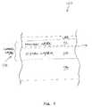
- FIG. 1is a cross-sectional view of a portion of a semiconductor-based device 100 .
- the device 100includes a channel layer 110 , which is preferably a surface channel layer (i.e., in contact with a dielectric layer).
- the channel layer 110includes a proximal layer 111 and a distal layer 112 .
- the channel layer 110optionally can include one or more intermediate layers 113 , though preferably the distal layer 112 and the proximal layer 111 are in contact with each other. Further, the proximal layer 111 is preferably in contact with a dielectric layer 120 .
- the channel layer 110further, and optionally, is in contact with a substrate layer 130 .
- the substrate layer 130such as a relaxed SiGe layer, can control, in part, the level of strain in the distal layer 112 and the proximal layer 111 .
- the channel layer 110provides both an n-channel for at least one NMOS component and a p-channel for at least one PMOS component.
- the componentscan be MOS transistors, for example, NMOS and PMOS transistors in an inverter, sharing the same surface channel layer.
- the channel layer 110provides a dual channel via appropriate selection, in part, of layer thicknesses and compositions.
- the proximal layer 111is a silicon layer under a tensile strain
- the distal layer 112is a germanium or Si 1 ⁇ y Ge y layer under a compressive strain
- the distal layer 112is in contact with the substrate layer 130 .
- the substrate layer 130includes a relaxed Si 1 ⁇ x Ge x layer having a lower concentration of germanium than that of the distal layer 112 .
- strain in the proximal layer 111is largely determined by the concentration of germanium in the relaxed Si 1 ⁇ x Ge x layer
- the strain in the distal layer 112is largely determined by the difference in germanium concentration between the distal layer 112 and the relaxed Si 1 ⁇ x Ge x substrate layer 130 .
- the proximal layer 111preferably has a thickness minimally sufficient to support electron conduction, that is, to provide an n-channel for one or more NMOS components.
- the silicon thicknessis approximately 5 nm.
- the channel layer 110then provides an enhanced hole mobility, in part due to the enhanced hole mobility provided by the compressive germanium or Si 1 ⁇ y Ge y distal layer.
- the distal layer 112in this implementation, has a band-gap offset relative to both the proximal layer 111 and the relaxed SiGe substrate layer 130 , which can promote confinement of the extended hole wave function within the compressed distal layer 112 . This effect can further promote enhanced hole mobility for a p-channel component in the device 100 .
- a compressively strained Si 1 ⁇ y Ge y layerhas a greater hole mobility than an unstrained Si 1 ⁇ y Ge y layer.
- a greater Ge concentrationcan also enhance hole mobility.
- this implementationcan reduce loss of mobility due to scattering of holes at the interface between the dielectric layer 120 and the proximal layer 111 .
- an enhancement-mode surface-channel MOS transistorforces carriers to traverse the transistor channel while very close to the gate dielectric interface.
- Such a transistorwhen implemented according to principles of the invention, can provide reduced hole scattering due, at least in part, to extension of the hole wave functions beyond the very thin proximal layer 111 .
- a strained-silicon proximal layer 111can still provide hole mobility that is enhanced relative to a conventional silicon surface-channel component.
- the combined proximal and distal layers 111 , 112can serve to provide highly enhanced hole mobility for p-channel components, while providing enhanced electron mobility for n-channel components.
- the electron mass in the vertical directioni.e., the surface normal direction
- the electron wave functionis relatively small in this direction, in comparison to the relatively large wave function for holes.
- electronscan be substantially confined within a relatively very thin layer.
- a strained-silicon layer of approximately 5 nm thicknesscan support substantially the entire wave function of an electron, while permitting a large portion of a hole wave function to extend beyond the strained-silicon layer.
- FIGS. 2A and 2Bshow band diagrams, which illustrate the behavior of electrons and holes for the implementation described above.
- FIG. 2Aillustrates a NMOS component
- FIG. 2Billustrates a PMOS component, for embodiments with a tensile silicon proximal layer 111 and with a compressive Si 1 ⁇ y Ge y distal layer 112 .
- the diagramillustrates the confinement of electrons substantially within the proximal layer 111 .
- the diagramillustrates the distribution of holes between the proximal layer 111 and the distal layer 112 .
- a strained-silicon proximal layer 111 having a thickness of approximately 5 nmcan provide a good balance between the tradeoffs of electron confinement within the proximal layer 111 and extension of hole wave function into the distal layer 112 . Thicknesses and compositions of layers in some embodiments that utilize silicon and germanium are described next.
- the distal layer 112is essentially 100% germanium.
- the thickness of the distal layer 112is preferably in a range of approximately 5 nm to approximately 18 nm.
- the distal layer 112is in contact with a substrate layer 130 of relaxed SiGe having a concentration preferably in a range of approximately 60 atomic % Ge to approximately 80 atomic % germanium.
- This compositioncan provide an effective level of compressive strain in the distal layer 112 while the germanium concentration in the distal layer 112 (i.e., 100% ) further improves hole mobility.
- An implementation having a distal layer 112 of germanium, as just described,can lead to stresses in a proximal layer 111 of silicon that will lead to partial or complete relaxation of the silicon. This is so because a pure germanium distal layer 112 is preferably formed on a substrate layer 130 having a relatively high concentration of germanium; the high concentration substrate layer 130 will generally have a relatively very high lattice mismatch relative to the silicon of the proximal layer 111 .
- Reduction in the concentration of germanium in the substrate layer 130 , and related reduction of germanium in the distal layer 112can substantially reduce or eliminate relaxation of the proximal layer 111 .
- a relatively high level of tensile stress in the proximal layer 111can be maintained.
- a substrate layer 130 of relaxed SiGe having a composition of approximately 40 atomic % Gecan be used in combination with a distal layer 112 having a composition in a range of approximately 60 atomic % Ge to approximately 80 atomic % germanium.
- Reduced stress in a silicon proximal layer 111 due to this implementationcan preserve the benefits of a tensilely strained silicon layer.
- the proximal layer 111can be reduced in thickness when used in combination with a substrate layer 130 having a relatively large lattice mismatch that will cause a correspondingly large stress in the proximal layer 111 .
- some thickness of the proximal layer 111can be sacrificed to preserve a tensile strain in the proximal layer 111 .
- FIG. 3is a cross-sectional view of an embodiment of a transistor 300 that can be included in a device, according to principles of the invention.
- the transistor 300includes a gate contact 350 , source and drain silicide contacts 340 , a gate oxide layer 320 , a channel layer (shared with other components in the device) including a tensile-silicon proximal layer 311 and a compressive Si 1 ⁇ y Ge y distal layer 312 , a relaxed Si 1 ⁇ x Ge x substrate layer 330 , and a silicon substrate 360 .
- the gate contact 350can include a doped conductive polycrystalline silicon (“polysilicon”) lower portion 351 proximal to the gate oxide 320 and a gate silicide upper portion 352 .
- the tensile silicon proximal layer 311 and the compressive Si 1 ⁇ y Ge y distal layer 312can be epitaxially grown on the relaxed Si 1 ⁇ x Ge x layer 330 . These layers provide a channel layer for the transistor 300 .
- the source and drain contacts 340can be formed, for example, by depositing a metal layer and reacting the metal layer with the channel layer and the relaxed SiGe layer 360 .
- the gate oxide 320is formed on the proximal layer 311 , possibly consuming a portion of the surface of the strained silicon.
- the dielectric layer 320can be formed by various methods conventional in the art, e.g., thermal oxidation or a deposition technique.
- the gate oxide 320can be, for example, a 1.5 to 10.0 nm thick layer of silicon dioxide.
- Other embodimentsinclude other suitable dielectric materials, e.g., silicon oxynitride, silicon nitride, a plurality of silicon nitride and silicon oxide layers, or a high-k dielectric.
- the transistor 300can be implemented as a NMOS or a PMOS component.
- the transistor 300can include, for example, different doping types and levels in the channel layer.
- a devicecan thus include NMOS and PMOS transistors 300 , utilizing a common channel layer, and both NMOS and PMOS components can provide improved surface channel transistor performance.
- FIG. 4is a cross-sectional view of a device 400 that includes a PMOS transistor 300 A and a NMOS transistor 300 B.
- the transistors 300 A, 300 Bhave structures and compositions similar to the embodiment described with respect to FIG. 3.
- the transistors 300 A, 300 Binclude gate contacts 350 A, 350 B, source and drain silicide contacts 340 A, 340 B, and gate oxide portions 320 A, 320 B.
- the transistors 300 A, 300 Bshare a channel layer 410 that includes a tensile silicon proximal layer 411 and a compressive Si 1 ⁇ y Ge y distal layer 412 .
- the transistors 300 A, 300 Balso share a relaxed Si 1 ⁇ x Ge x substrate layer 430 and a silicon substrate 360 .
- the deviceincludes an n-type implanted dopant well 420 , within which the PMOS transistor 300 A resides.
- the dopant well 420can be formed via any of a variety of methods known in the semiconductor fabrication arts.
- the transistors 300 A, 300 Bare electrically isolated from each other via a shallow trench isolation (STI) portion 490 .
- STIshallow trench isolation
- the isolation 490preferably is deep enough to cross the channel layer 410 , ending at least in the SiGe relaxed substrate layer 430 .
- the isolation 490is absent or replaced by other isolation means.
- one embodimentincludes semi-recessed oxide isolation (S-ROX) portions.
- the proximal layer 411 in the vicinity of the PMOS transistor 300 Ais thinned prior to formation of the gate oxide portions 320 A.
- the thinned proximal layer 411is indicated by the dashed line A in FIG. 4.
- This alternativecan provide a further enhancement of the hole mobility in the channel layer 410 for the PMOS transistor 300 A.
- Table Ilists values of relative inverter stage delay (t p ) as a function of transistor parameters for seven illustrative inverters.
- the parametersinclude: e n and e p , the enhancement factors, respectively, for the NMOS and PMOS transistor drive currents; ⁇ p , the relative width change of the PMOS transistor (i.e., PMOS transistor width of an illustrative transistor divided by the width of a standard PMOS transistor of a standard reference inverter); and ⁇ n , the relative width change of the NMOS transistor of an illustrative inverter.
- inverter stage delaycan be reduced to increase inverter performance without decreasing transistor gate length.
- Table Iillustrates the effect of drive current enhancements as well as adjustments of device width on the relative decrease in inverter delay time.
- the first rowrepresents a standard reference inverter (that is, no delay decrease).
- the second rowrepresents an inverter having a strained-silicon channel directly on a relaxed Si 0.8 Ge 0.2 substrate.
- the electron enhancement factoris 1.8, with the assumption that the hole enhancement has approximately disappeared during processing, leaving an e p of 1.
- the delay for this inverteris reduced by a factor of 0.78 relative to the reference inverter.
- the third rowillustrates an inverter having a strained-silicon layer directly on a relaxed Si 0.6 Ge 0.4 substrate.
- the hole mobility enhancement in the example PMOS componentis 1.8.
- the electron and hole enhancementshave been selected to be the same.
- This example inverter designcan be particularly advantageous for porting legacy digital circuit designs, since the ratio of NMOS and PMOS mobility has not changed from that of conventional silicon-based inverters.
- the fourth rowis representative of an inverter in which the NMOS and PMOS transistors include a compressive Ge distal layer and a silicon proximal layer, according to principles of the invention.
- the hole enhancementcan be, for example, as high as approximately 7.
- Both the NMOS and PMOS deviceshave very high carrier mobilities, and the mobilities are approximately the same.
- the illustrative inverterhas NMOS and PMOS transistors that are symmetric, i.e., the transitors have the same drive current by adjusting the NMOS component gate width by a factor of approximately 2.
- the illustrative inverterhas a silicon proximal layer that has been thinned for both the PMOS and NMOS transistors, and which resides on a compressive germanium distal layer; the electron wave function, as well as the hole wave function, is predominately located in the compressed Ge layer.
- the PMOS transistor widthhas been adjusted to make the transistor currents symmetrical.
- FIG. 5illustrates inverter stage delay as a function of gate length variations, associated with the seven illustrative inverters of Table I.
- the top curve(the conventional, and slowest, inverter) corresponds to the first row of Table I.
- inverters that include dual-channel layersi.e., a channel layer having a proximal layer and a distal layer according to principles of the invention, can provide performance improvement without reducing device feature dimensions.
- some embodiments of the inventionutilize a substrate that includes a SiGe substrate layer.
- the SiGe substrate layercan be grown on a silicon wafer, and can include more than one layer of alloys of varying composition, thickness and growth conditions.
- the substrate layercan include a SiGe layer or multiple SiGe layers and/or SiGe layers having a graded composition.
- the SiGe layerincludes a relaxed SiGe layer grown on intermediate SiGe layers that accommodate the lattice mismatch with a silicon wafer.
- the substratecan include, for example, a silicon wafer, with the SiGe layers grown on the silicon wafer.
- an oxide layercan be present between the silicon wafer and the SiGe layer.
- Other types of materialscan provide a base or substrate, e.g., silicon-on-insulator (SOI) wafers, germanium wafers, glass substrates and laminated substrates.
- SOIsilicon-on-insulator
- Silicon, germanium and SiGe layerscan be formed, for example, via known epitaxial growth techniques. Growth of silicon, germanium or SiGe layers of suitable composition and thickness on a SiGe relaxed layer, enables production of a channel layer of controlled stress and dislocation density.
- SiGe substratesin which the Ge content can be up to 100%, include: a relaxed, uniform composition SiGe layer on a graded composition SiGe layer atop a Si substrate; a relaxed, uniform composition SiGe layer directly adjacent to a Si substrate; and a relaxed, uniform composition SiGe layer on an insulating layer like SiO 2 , adjacent a Si substrate.
Landscapes
- Insulated Gate Type Field-Effect Transistor (AREA)
- Metal-Oxide And Bipolar Metal-Oxide Semiconductor Integrated Circuits (AREA)
Abstract
Description
- This application claims benefit of and priority to U.S. Provisional Patent Application Serial No. 60/311,188, filed Aug. 9, 2001, the entire contents of which are incorporated herein by reference.[0001]
- The invention generally relates to semiconductor devices, and, more particularly, to the fabrication and structure of devices that include metal-oxide-semiconductor type components.[0002]
- Newer types of substrates can be used as replacements for traditional silicon wafers to improve silicon-based electronic device performance. For example, wafers that have a silicon-germanium (SiGe) alloy layer can provide improved channel-layer performance in a strained-silicon layer grown on a relaxed, i.e., relatively strain-free, SiGe layer. Strained silicon can provide improved minority carrier mobility for a surface-channel layer in, for example, metal-oxide-semiconductor (MOS) field-effect transistors (FET).[0003]
- The carrier mobility of the silicon channel layer generally increases with the level of strain in the layer. The level of strain is determined by the lattice mismatch with the underlying relaxed SiGe layer. The lattice mismatch, in turn, is determined by the Ge concentration of the relaxed SiGe layer. That is, the lattice spacing of a relaxed SiGe layer generally increases with increasing Ge concentration.[0004]
- Thus, as the Ge concentration in a relaxed SiGe substrate layer is increased, the electron mobility in the overlying strained-silicon channel layer generally increases. The electron mobility generally saturates beyond a Ge concentration of approximately 20 atomic %, but the hole mobility continues to increase as the Ge concentration rises.[0005]
- The behavior of electron and hole mobility is of particular significance, for example, in the performance of an inverter, one of the basic building blocks of integrated circuit devices. An inverter includes both an NMOS (i.e., n-channel) and PMOS (i.e., p-channel) transistor, and the inverter delay is dependent upon both the NMOS and PMOS transistor drive currents. With mobility enhancements of the electron and hole charge carriers, the drive current increases, and the inverter stage delay decreases.[0006]
- where K[0008]i=CvsatCoxWi, “i” represents p or n, and tpis the total inverter delay time. The delay is related to the ability of the NMOS and PMOS transistors to drive the inverter capacitance, CL. Kpand Knare, respectively, related to the transconductance of the PMOS and NMOS transistors. C is a constant, Vsatis the saturation velocity of the carrier in the channel, Coxis the gate capacitance per unit area, and Wiis the width of the corresponding NMOS or PMOS transistor (i.e., the width of the gate).
- where B is a constant, e[0010]pis the enhancement factor in PMOS drive current due to channel improvement relative to a standard silicon component (e.g., through use of strained-silicon), enis the enhancement factor in NMOS drive current, ωpis any relative width change in the PMOS transistor (new width divided by the width of standard a standard silicon PMOS component in a reference standard inverter), and ωnis any relative width change in the NMOS transistor. This expression is an approximation because any large change in device width can affect the constant B, which is associated with the overall inverter capacitance.
- A standard Si inverter is typically optimized to minimize stage delay by widening the PMOS transistor in order to balance the current drive in the NMOS and PMOS transistors. This requirement arises because standard silicon devices have a much higher NMOS drive current than PMOS drive current (due to electrons having a much higher mobility than holes in unstrained silicon).[0011]
- Strained silicon with 20 atomic % Ge on a relaxed SiGe substrate can increase electron mobility by approximately 80%, with a hole mobility at best only slightly enhanced. Thus, strained silicon can cause an increase in mobility mismatch, and, therefore, an increase in drive current mismatch between the NMOS and PMOS transistors in the inverter. Therefore, the inverter stage delay generally does not decrease by a full 80% when strained silicon is employed as a channel layer.[0012]
- As the germanium concentration in a relaxed SiGe substrate rises to 30% and to 40%, the hole mobility increases, respectively, by approximately 40% and over 100%. Beyond a concentration of 40%, little or no further enhancement of the hole mobility occurs. At 40% Ge in the relaxed SiGe substrate, the ratio of the drive currents in the NMOS and PMOS transistors generally is nearly the same ratio as in a standard device.[0013]
- Thus, asymmetrical mobilities and transistor sizes remain a problem for inverters and other semiconductor devices.[0014]
- The invention involves structures and fabrication methods for semiconductor devices that include a channel layer having a dual-layer structure. The channel layer is preferably a shared surface-channel layer for more than one component in the device. The channel layer provides enhanced electron mobility and, in particular, enhanced hole mobility. The channel layer can serve as a surface channel layer for both PMOS and NMOS components fabricated on a common substrate.[0015]
- The dual-layer structure preferably includes a silicon layer that overlies and is preferably in contact with a Si[0016]1−yGeyor germanium layer. The silicon layer preferably is in contact with a gate dielectric.
- Inverters, according to principles of the invention, can be fabricated with PMOS and NMOS transistors of similar size. The inverters can then consume less space on a substrate, in comparison to asymmetrical inverters. The inverters can have a stage delay that is decreased relative to other inverters.[0017]
- Accordingly, in a first aspect, the invention features a semiconductor-based device, which includes a channel layer. The channel layer includes a distal layer and a proximal layer in contact with the distal layer. The distal layer supports at least a portion of hole conduction for at least one p-channel component. The proximal layer has a thickness that permits a hole wave function to effectively extend from the proximal layer into the distal layer to facilitate hole conduction by the distal layer. The proximal layer supports at least a portion of electron conduction for at least one n-channel component.[0018]
- Each p-channel component can include a p-channel transistor, and each n-channel component can include an n-channel transistor. The components thus can share a common channel layer, and can be operated as surface channel layer components. The n-channel transistor and the p-channel transistor can be associated with, for example, an inverter.[0019]
- By enhancing hole mobility even more than electron mobility, inverters having transistors of a similar area size or having a similar dimension can be fabricated. For example, n-channel and p-channel transistors can be fabricated with similar gate lengths or gate widths.[0020]
- The thickness of the proximal layer can be less for the p-channel component than for the n-channel component, to extend a greater portion of hole wave functions from the proximal layer into the distal layer.[0021]
- The proximal layer is preferably under tensile strain. This can be accomplished, for example, with a silicon proximal layer adjacent to a SiGe substrate layer.[0022]
- The distal layer is preferably under compressive strain. This can be accomplished, for example, with a SiGe distal layer having a higher germanium concentration than an underlying SiGe substrate layer.[0023]
- Alternatively, the proximal layer can be formed from silicon, and the thickness of the silicon layer can be in a range of approximately 4 nm to approximately 10 nm, preferably 5 nm, to support electron conduction within the proximal layer. The thickness of the distal layer can be in a range of approximately 5 nm to approximately 18 nm.[0024]
- The device can also include a dielectric layer in contact with the proximal layer. The proximal layer can be formed of strained silicon, and the distal layer formed of strained germanium or of strained SiGe alloy.[0025]
- The device can further include a relaxed SiGe substrate layer in contact with the distal layer, the relaxed SiGe layer having a germanium concentration in a range of approximately 30 atomic % to approximately 85 atomic %.[0026]
- In a second aspect, the invention features a method for fabricating a semiconductor-based device. The method includes provision of a distal portion of a channel layer, and provision of a proximal portion of the channel layer, the proximal portion being in contact with the distal portion.[0027]
- Provision of the proximal portion can include thinning the proximal portion in a location of each p-channel component to enhance the support of hole conduction. Thinning can include reducing the thickness of the proximal layer in the location of each p-channel component while leaving the thickness substantially unchanged in a location of at least one n-channel component.[0028]
- In the drawings, like reference characters generally refer to the same parts throughout the different views. Also, the drawings are not necessarily to scale, emphasis instead generally being placed upon illustrating the principles of the invention.[0029]
- FIG. 1 is cross-sectional view of a portion of an embodiment of a semiconductor-based device.[0030]
- FIG. 2A is a band diagram that illustrates the behavior of electrons for an illustrative NMOS component implementation of the embodiment of FIG. 1.[0031]
- FIG. 2B is a band diagram that illustrates the behavior of holes for an illustrative PMOS component implementation of the embodiment of FIG. 1.[0032]
- FIG. 3 is a cross-sectional view of an embodiment of a transistor that can be included in a device, according to principles of the invention.[0033]
- FIG. 4 is a cross-sectional view of an embodiment of a device that includes a PMOS transistor and a NMOS transistor.[0034]
- FIG. 5 is a graph of inverter stage delay as a function of gate length data, associated with seven illustrative inverters.[0035]
- The invention provides improved semiconductor device designs, for example, improved inverter design. Various features of the invention are well suited to applications utilizing MOS transistors that include, for example, Si, Si[0036]1−xGexand/or Ge layers in and or on a substrate.
- The term “MOS” is here used to refer generally to semiconductor devices that include a conductive gate spaced at least by an insulting layer from a semiconducting channel layer. The terms “SiGe” and “Si[0037]1−xGex” are here used interchangeably to refer to silicon-germanium alloys. The term “silicide” is here used to refer to a reaction product of a metal, silicon, and optionally other components, such as germanium. The term “silicide” is also used, less formally, to refer to the reaction product of a metal with an elemental semiconductor, a compound semiconductor or an alloy semiconductor.
- First, with reference to FIG. 1, some general principles of the invention are described in broad overview. FIG. 1 is a cross-sectional view of a portion of a semiconductor-based[0038]
device 100. Thedevice 100 includes achannel layer 110, which is preferably a surface channel layer (i.e., in contact with a dielectric layer). Thechannel layer 110 includes a proximal layer111 and adistal layer 112. - The[0039]
channel layer 110 optionally can include one or moreintermediate layers 113, though preferably thedistal layer 112 and the proximal layer111 are in contact with each other. Further, the proximal layer111 is preferably in contact with adielectric layer 120. - The[0040]
channel layer 110 further, and optionally, is in contact with asubstrate layer 130. Thesubstrate layer 130, such as a relaxed SiGe layer, can control, in part, the level of strain in thedistal layer 112 and the proximal layer111. - The[0041]
channel layer 110 provides both an n-channel for at least one NMOS component and a p-channel for at least one PMOS component. The components can be MOS transistors, for example, NMOS and PMOS transistors in an inverter, sharing the same surface channel layer. Thechannel layer 110 provides a dual channel via appropriate selection, in part, of layer thicknesses and compositions. - Although principles of the invention can be applied to devices fabricated from a wide variety of materials, including a wide variety of semiconductor materials, for simplicity, the following description will focus on embodiments that include silicon, germanium and SiGe alloys.[0042]
- In one implementation of the[0043]
device 100, the proximal layer111 is a silicon layer under a tensile strain, thedistal layer 112 is a germanium or Si1−yGeylayer under a compressive strain, and thedistal layer 112 is in contact with thesubstrate layer 130. Thesubstrate layer 130 includes a relaxed Si1−xGexlayer having a lower concentration of germanium than that of thedistal layer 112. Thus strain in the proximal layer111 is largely determined by the concentration of germanium in the relaxed Si1−xGexlayer, while the strain in thedistal layer 112 is largely determined by the difference in germanium concentration between thedistal layer 112 and the relaxed Si1−xGexsubstrate layer130. - The proximal layer[0044]111 preferably has a thickness minimally sufficient to support electron conduction, that is, to provide an n-channel for one or more NMOS components. For a silicon layer of the presently described implementation, the silicon thickness is approximately 5 nm.
- For silicon thicknesses less than approximately 4 nm, some loss of electron mobility will generally occur. Hole mobility in the[0045]
channel layer 110, however, generally benefits from reduction in the thickness of the proximal layer111. The wave function of a hole, perpendicular to thechannel layer 110 interfaces, is relatively large due to a relatively small mass of holes in this direction. Thus, in the case of a silicon proximal layer111, a hole wave function generally extends well beyond the silicon proximal layer111 into the underlyingdistal layer 112. - The[0046]
channel layer 110 then provides an enhanced hole mobility, in part due to the enhanced hole mobility provided by the compressive germanium or Si1−yGeydistal layer. Thedistal layer 112, in this implementation, has a band-gap offset relative to both the proximal layer111 and the relaxedSiGe substrate layer 130, which can promote confinement of the extended hole wave function within the compresseddistal layer 112. This effect can further promote enhanced hole mobility for a p-channel component in thedevice 100. - The above-described implementation provides enhanced hole mobility via a number of means. For example, a compressively strained Si[0047]1−yGeylayer has a greater hole mobility than an unstrained Si1−yGeylayer. A greater Ge concentration can also enhance hole mobility.
- Further, this implementation can reduce loss of mobility due to scattering of holes at the interface between the[0048]
dielectric layer 120 and the proximal layer111. For example, an enhancement-mode surface-channel MOS transistor, as known in the semiconductor arts, forces carriers to traverse the transistor channel while very close to the gate dielectric interface. Such a transistor, when implemented according to principles of the invention, can provide reduced hole scattering due, at least in part, to extension of the hole wave functions beyond the very thin proximal layer111. - Although the mobility of holes in the[0049]
distal layer 112 will generally be greater than that in the proximal layer111, a strained-silicon proximal layer111 can still provide hole mobility that is enhanced relative to a conventional silicon surface-channel component. Thus, the combined proximal anddistal layers 111,112 can serve to provide highly enhanced hole mobility for p-channel components, while providing enhanced electron mobility for n-channel components. - The electron mass in the vertical direction, i.e., the surface normal direction, is relatively large in strained silicon. Thus, the electron wave function is relatively small in this direction, in comparison to the relatively large wave function for holes. Hence, electrons can be substantially confined within a relatively very thin layer. As indicated above, a strained-silicon layer of approximately 5 nm thickness can support substantially the entire wave function of an electron, while permitting a large portion of a hole wave function to extend beyond the strained-silicon layer.[0050]
- FIGS. 2A and 2B show band diagrams, which illustrate the behavior of electrons and holes for the implementation described above. FIG. 2A illustrates a NMOS component and FIG. 2B illustrates a PMOS component, for embodiments with a tensile silicon proximal layer[0051]111 and with a compressive Si1−yGey
distal layer 112. For the NMOS component, the diagram illustrates the confinement of electrons substantially within the proximal layer111. For the PMOS component, the diagram illustrates the distribution of holes between the proximal layer111 and thedistal layer 112. - As described above, a strained-silicon proximal layer[0052]111 having a thickness of approximately 5 nm can provide a good balance between the tradeoffs of electron confinement within the proximal layer111 and extension of hole wave function into the
distal layer 112. Thicknesses and compositions of layers in some embodiments that utilize silicon and germanium are described next. - In one implementation, the[0053]
distal layer 112 is essentially 100% germanium. The thickness of thedistal layer 112 is preferably in a range of approximately 5 nm to approximately 18 nm. Thedistal layer 112 is in contact with asubstrate layer 130 of relaxed SiGe having a concentration preferably in a range of approximately 60 atomic % Ge to approximately 80 atomic % germanium. This composition can provide an effective level of compressive strain in thedistal layer 112 while the germanium concentration in the distal layer112 (i.e., 100% ) further improves hole mobility. - An implementation having a[0054]
distal layer 112 of germanium, as just described, can lead to stresses in a proximal layer111 of silicon that will lead to partial or complete relaxation of the silicon. This is so because a pure germaniumdistal layer 112 is preferably formed on asubstrate layer 130 having a relatively high concentration of germanium; the highconcentration substrate layer 130 will generally have a relatively very high lattice mismatch relative to the silicon of the proximal layer111. - Reduction in the concentration of germanium in the[0055]
substrate layer 130, and related reduction of germanium in thedistal layer 112 can substantially reduce or eliminate relaxation of the proximal layer111. Thus, a relatively high level of tensile stress in the proximal layer111 can be maintained. - For example, a[0056]
substrate layer 130 of relaxed SiGe having a composition of approximately 40 atomic % Ge can be used in combination with adistal layer 112 having a composition in a range of approximately 60 atomic % Ge to approximately 80 atomic % germanium. Reduced stress in a silicon proximal layer111 due to this implementation can preserve the benefits of a tensilely strained silicon layer. - As another alternative, the proximal layer[0057]111 can be reduced in thickness when used in combination with a
substrate layer 130 having a relatively large lattice mismatch that will cause a correspondingly large stress in the proximal layer111. Thus, some thickness of the proximal layer111 can be sacrificed to preserve a tensile strain in the proximal layer111. - FIG. 3 is a cross-sectional view of an embodiment of a[0058]
transistor 300 that can be included in a device, according to principles of the invention. Thetransistor 300 includes agate contact 350, source and drainsilicide contacts 340, agate oxide layer 320, a channel layer (shared with other components in the device) including a tensile-siliconproximal layer 311 and a compressive Si1−yGeydistal layer 312, a relaxed Si1−xGexsubstrate layer330, and asilicon substrate 360. Thegate contact 350 can include a doped conductive polycrystalline silicon (“polysilicon”)lower portion 351 proximal to thegate oxide 320 and a gate silicideupper portion 352. - The tensile silicon[0059]
proximal layer 311 and the compressive Si1−yGeydistal layer 312 can be epitaxially grown on the relaxed Si1−xGexlayer330. These layers provide a channel layer for thetransistor 300. The source anddrain contacts 340 can be formed, for example, by depositing a metal layer and reacting the metal layer with the channel layer and therelaxed SiGe layer 360. - The[0060]
gate oxide 320 is formed on theproximal layer 311, possibly consuming a portion of the surface of the strained silicon. Thedielectric layer 320 can be formed by various methods conventional in the art, e.g., thermal oxidation or a deposition technique. - The[0061]
gate oxide 320 can be, for example, a 1.5 to 10.0 nm thick layer of silicon dioxide. Other embodiments include other suitable dielectric materials, e.g., silicon oxynitride, silicon nitride, a plurality of silicon nitride and silicon oxide layers, or a high-k dielectric. - The[0062]
transistor 300, according to principles of the invention, can be implemented as a NMOS or a PMOS component. Thetransistor 300 can include, for example, different doping types and levels in the channel layer. A device can thus include NMOS andPMOS transistors 300, utilizing a common channel layer, and both NMOS and PMOS components can provide improved surface channel transistor performance. - Referring now to FIG. 4, features of the invention that permit improved inverters are described. FIG. 4 is a cross-sectional view of a[0063]
device 400 that includes a PMOS transistor300A and aNMOS transistor 300B. Thetransistors 300A,300B have structures and compositions similar to the embodiment described with respect to FIG. 3. - The[0064]
transistors 300A,300B include gate contacts350A,350B, source and drainsilicide contacts gate oxide portions 320A,320B. Thetransistors 300A,300B share a channel layer410 that includes a tensile silicon proximal layer411 and a compressive Si1−yGeydistal layer 412. Thetransistors 300A,300B also share a relaxed Si1−xGexsubstrate layer430 and asilicon substrate 360. - The device includes an n-type implanted dopant well[0065]420, within which the PMOS transistor300A resides. The dopant well420 can be formed via any of a variety of methods known in the semiconductor fabrication arts. The
transistors 300A,300B are electrically isolated from each other via a shallow trench isolation (STI)portion 490. - The[0066]
isolation 490 preferably is deep enough to cross the channel layer410, ending at least in the SiGerelaxed substrate layer 430. In other embodiments, theisolation 490 is absent or replaced by other isolation means. For example, one embodiment includes semi-recessed oxide isolation (S-ROX) portions. - In an alternative implementation of the[0067]
device 400, the proximal layer411 in the vicinity of the PMOS transistor300A is thinned prior to formation of thegate oxide portions 320A. The thinned proximal layer411 is indicated by the dashed line A in FIG. 4. This alternative can provide a further enhancement of the hole mobility in the channel layer410 for the PMOS transistor300A. - Some benefits of the invention when applied to inverter fabrication are described below, with a few illustrative embodiments.[0068]
TABLE I Row ωn ωp en ep Relative t p1 1 1 1 1 1 2 1 1 1.8 1 0.78 3 1 1 1.8 1.8 0.56 4 1 1 1.8 7 0.35 5 2 1 1.8 7 0.21 6 2 1 2.17 7 0.19 7 2 1.17 2.17 7 0.176 - Table I, above, lists values of relative inverter stage delay (t[0069]p) as a function of transistor parameters for seven illustrative inverters. The parameters include: enand ep, the enhancement factors, respectively, for the NMOS and PMOS transistor drive currents; ωp, the relative width change of the PMOS transistor (i.e., PMOS transistor width of an illustrative transistor divided by the width of a standard PMOS transistor of a standard reference inverter); and ωn, the relative width change of the NMOS transistor of an illustrative inverter.
- As shown in the listed examples, inverter stage delay can be reduced to increase inverter performance without decreasing transistor gate length. Table I illustrates the effect of drive current enhancements as well as adjustments of device width on the relative decrease in inverter delay time.[0070]
- The first row represents a standard reference inverter (that is, no delay decrease). The second row represents an inverter having a strained-silicon channel directly on a relaxed Si[0071]0.8Ge0.2substrate. In this case, the electron enhancement factor is 1.8, with the assumption that the hole enhancement has approximately disappeared during processing, leaving an epof 1. The delay for this inverter is reduced by a factor of 0.78 relative to the reference inverter.
- The third row illustrates an inverter having a strained-silicon layer directly on a relaxed Si[0072]0.6Ge0.4substrate. The hole mobility enhancement in the example PMOS component is 1.8.
- Further, in this example, the electron and hole enhancements have been selected to be the same. This example inverter design can be particularly advantageous for porting legacy digital circuit designs, since the ratio of NMOS and PMOS mobility has not changed from that of conventional silicon-based inverters.[0073]
- The fourth row is representative of an inverter in which the NMOS and PMOS transistors include a compressive Ge distal layer and a silicon proximal layer, according to principles of the invention. In this case, the hole enhancement can be, for example, as high as approximately 7. Both the NMOS and PMOS devices have very high carrier mobilities, and the mobilities are approximately the same.[0074]
- In the fifth row, the illustrative inverter has NMOS and PMOS transistors that are symmetric, i.e., the transitors have the same drive current by adjusting the NMOS component gate width by a factor of approximately 2.[0075]
- In the sixth row, the illustrative inverter has a silicon proximal layer that has been thinned for both the PMOS and NMOS transistors, and which resides on a compressive germanium distal layer; the electron wave function, as well as the hole wave function, is predominately located in the compressed Ge layer.[0076]
- In the final row, i.e., the seventh, the PMOS transistor width has been adjusted to make the transistor currents symmetrical.[0077]
- As illustrated by Table I, application of features of the invention to inverter design can reduce inverter delay by up to 82% or more. Thus, for example, digital circuit performance can be greatly improved without resorting to decreases in transistor gate length.[0078]
- FIG. 5 illustrates inverter stage delay as a function of gate length variations, associated with the seven illustrative inverters of Table I. The top curve (the conventional, and slowest, inverter) corresponds to the first row of Table I. As illustrated, inverters that include dual-channel layers, i.e., a channel layer having a proximal layer and a distal layer according to principles of the invention, can provide performance improvement without reducing device feature dimensions.[0079]
- As indicated above, some embodiments of the invention utilize a substrate that includes a SiGe substrate layer. The SiGe substrate layer can be grown on a silicon wafer, and can include more than one layer of alloys of varying composition, thickness and growth conditions. Thus, the substrate layer can include a SiGe layer or multiple SiGe layers and/or SiGe layers having a graded composition. In some embodiments, the SiGe layer includes a relaxed SiGe layer grown on intermediate SiGe layers that accommodate the lattice mismatch with a silicon wafer.[0080]
- The substrate can include, for example, a silicon wafer, with the SiGe layers grown on the silicon wafer. In this case, an oxide layer can be present between the silicon wafer and the SiGe layer. Other types of materials can provide a base or substrate, e.g., silicon-on-insulator (SOI) wafers, germanium wafers, glass substrates and laminated substrates.[0081]
- Silicon, germanium and SiGe layers can be formed, for example, via known epitaxial growth techniques. Growth of silicon, germanium or SiGe layers of suitable composition and thickness on a SiGe relaxed layer, enables production of a channel layer of controlled stress and dislocation density. Examples of SiGe substrates, in which the Ge content can be up to 100%, include: a relaxed, uniform composition SiGe layer on a graded composition SiGe layer atop a Si substrate; a relaxed, uniform composition SiGe layer directly adjacent to a Si substrate; and a relaxed, uniform composition SiGe layer on an insulating layer like SiO[0082]2, adjacent a Si substrate.
- Variations, modifications, and other implementations of what is described herein will occur to those of ordinary skill in the art without departing from the spirit and the scope of the invention as claimed. Accordingly, the invention is to be defined not by the preceding illustrative description but instead by the spirit and scope of the following claims.[0083]


Claims (30)
1. A semiconductor-based device, comprising:
a channel layer, comprising:
a distal layer to support at least a portion of hole conduction for at least one p-channel component; and
a proximal layer to support at least a portion of an electron current for at least one n-channel component, the proximal layer being in contact with the distal layer and having a thickness that permits a hole wave function to effectively extend from the proximal layer into the distal layer to facilitate hole conduction by the distal layer.
2. The device ofclaim 1 , wherein the proximal layer has a tensile strain.
3. The device ofclaim 1 , wherein the at least one p-channel component comprises a p-channel transistor, the at least one n-channel component comprises an n-channel transistor.
4. The device ofclaim 3 , wherein the n-channel transistor and the p-channel transistor are associated with an inverter.
5. The device ofclaim 4 , wherein a gate width of the n-channel transistor and a gate width of the p-channel transistor are approximately the same.
6. The device ofclaim 4 , wherein a gate length of the n-channel transistor and a gate length of the p-channel transistor are approximately the same.
7. The device ofclaim 4 , wherein a hole mobility of the p-channel transistor and an electron mobility of the n-channel transistor are approximately the same.
8. The device ofclaim 1 , wherein the thickness of the proximal layer is less for the p-channel component than for the n-channel component.
9. The device ofclaim 8 , wherein the proximal layer has zero thickness for the p-channel component.
10. The device ofclaim 1 , wherein the proximal layer consists essentially of silicon, and the thickness of the proximal layer is in a range of approximately 4 nm to approximately 10 nm.
11. The device ofclaim 10 , wherein the thickness of the proximal layer is approximately 5 nm.
12. The device ofclaim 10 , wherein the thickness of the distal layer is in a range of approximately 5 nm to approximately 18 nm.
13. The device ofclaim 1 , wherein the proximal layer supports substantially all of an electron current for at least one n-channel component.
14. The device ofclaim 1 , wherein the distal layer supports at least a portion an electron current for at least one n-channel component.
15. The device ofclaim 14 , wherein the thickness of the proximal layer is less than approximately 5 nm.
16. The device ofclaim 1 , further comprising a dielectric layer in contact with the proximal layer, the proximal layer being located between the dielectric layer and the distal layer.
17. The device ofclaim 1 , wherein the proximal layer consists essentially of silicon, and the distal layer consists essentially of germanium.
18. The device ofclaim 17 , further comprising a relaxed SiGe layer in contact with the distal layer, the relaxed SiGe layer having a germanium concentration in a range of approximately 60 atomic % to approximately 85 atomic %.
19. The device ofclaim 18 , wherein the proximal layer is at least partially relaxed.
20. The device ofclaim 1 , wherein the proximal layer consists essentially of silicon, and the distal layer consists essentially of silicon and germanium.
21. The device ofclaim 20 , further comprising a relaxed SiGe layer in contact with the distal layer, the relaxed SiGe layer having a germanium concentration in a range of approximately 30 atomic % to approximately 50 atomic %, and wherein the distal layer has a germanium concentration in a range of approximately 55 atomic % to approximately 85 atomic %.
22. The device ofclaim 21 , wherein the proximal layer is under substantially unrelieved tensile strain.
23. The device ofclaim 1 , wherein the distal layer is under compressive strain.
24. The device ofclaim 23 , further comprising a relaxed SiGe layer in contact with the distal layer, wherein the distal layer has a greater concentration of germanium than a concentration of germanium in the relaxed SiGe layer.
25. A method for fabricating a semiconductor-based device, the method comprising:
providing a distal portion of a channel layer to support hole conduction for at least one p-channel component; and
providing a proximal portion of the channel layer, the proximal portion being in contact with the distal portion and having a thickness that permits a hole wave function to effectively extend from the proximal portion into the distal portion to facilitate hole conduction by the distal portion.
26. The method ofclaim 25 , wherein providing the proximal portion comprises thinning the proximal portion in a location of the at least one p-channel component to enhance the support of hole conduction.
27. The method ofclaim 26 , wherein thinning comprises reducing the thickness of the proximal layer in the location of the at least one p-channel component while leaving the thickness substantially unchanged in a location of at least one n-channel component.
28. The method ofclaim 25 , further comprising providing a substrate layer comprising silicon and germanium, and wherein the proximal portion comprises tensilely strained silicon, and the distal portion comprises at least one of compressively strained silicon and germanium.
29. The method ofclaim 28 , wherein the thickness of the proximal layer is in a range of approximately 4 nm to 10 nm.
30. The method ofclaim 25 , further comprising forming the at least one p-channel component, and forming at least one n-channel component, the at least one p-channel component and the at least one n-channel each having the channel layer in contact with a dielectric layer.
Priority Applications (2)
| Application Number | Priority Date | Filing Date | Title |
|---|---|---|---|
| US10/216,085US6974735B2 (en) | 2001-08-09 | 2002-08-09 | Dual layer Semiconductor Devices |
| US11/130,575US7465619B2 (en) | 2001-08-09 | 2005-05-17 | Methods of fabricating dual layer semiconductor devices |
Applications Claiming Priority (2)
| Application Number | Priority Date | Filing Date | Title |
|---|---|---|---|
| US31118801P | 2001-08-09 | 2001-08-09 | |
| US10/216,085US6974735B2 (en) | 2001-08-09 | 2002-08-09 | Dual layer Semiconductor Devices |
Related Child Applications (1)
| Application Number | Title | Priority Date | Filing Date |
|---|---|---|---|
| US11/130,575ContinuationUS7465619B2 (en) | 2001-08-09 | 2005-05-17 | Methods of fabricating dual layer semiconductor devices |
Publications (2)
| Publication Number | Publication Date |
|---|---|
| US20030057439A1true US20030057439A1 (en) | 2003-03-27 |
| US6974735B2 US6974735B2 (en) | 2005-12-13 |
Family
ID=26910639
Family Applications (2)
| Application Number | Title | Priority Date | Filing Date |
|---|---|---|---|
| US10/216,085Expired - LifetimeUS6974735B2 (en) | 2001-08-09 | 2002-08-09 | Dual layer Semiconductor Devices |
| US11/130,575Expired - LifetimeUS7465619B2 (en) | 2001-08-09 | 2005-05-17 | Methods of fabricating dual layer semiconductor devices |
Family Applications After (1)
| Application Number | Title | Priority Date | Filing Date |
|---|---|---|---|
| US11/130,575Expired - LifetimeUS7465619B2 (en) | 2001-08-09 | 2005-05-17 | Methods of fabricating dual layer semiconductor devices |
Country Status (1)
| Country | Link |
|---|---|
| US (2) | US6974735B2 (en) |
Cited By (64)
| Publication number | Priority date | Publication date | Assignee | Title |
|---|---|---|---|---|
| US20030013323A1 (en)* | 2001-06-14 | 2003-01-16 | Richard Hammond | Method of selective removal of SiGe alloys |
| US20030034529A1 (en)* | 2000-12-04 | 2003-02-20 | Amberwave Systems Corporation | CMOS inverter and integrated circuits utilizing strained silicon surface channel MOSFETs |
| US20030052334A1 (en)* | 2001-06-18 | 2003-03-20 | Lee Minjoo L. | Structure and method for a high-speed semiconductor device |
| US20030077867A1 (en)* | 2001-03-02 | 2003-04-24 | Fitzergald Eugene A. | Relaxed silicon germanium platform for high speed CMOS electronics and high speed analog circuits |
| US20030102498A1 (en)* | 2001-09-24 | 2003-06-05 | Glyn Braithwaite | RF circuits including transistors having strained material layers |
| US20030113948A1 (en)* | 2000-01-20 | 2003-06-19 | Amberwave Systems Corporation | Low threading dislocation density relaxed mismatched epilayers without high temperature growth |
| US20030168654A1 (en)* | 2000-08-16 | 2003-09-11 | Massachusetts Institute Of Technology | Process for producing semiconductor article using graded epitaxial growth |
| US6649480B2 (en) | 2000-12-04 | 2003-11-18 | Amberwave Systems Corporation | Method of fabricating CMOS inverter and integrated circuits utilizing strained silicon surface channel MOSFETs |
| US20030215990A1 (en)* | 2002-03-14 | 2003-11-20 | Eugene Fitzgerald | Methods for fabricating strained layers on semiconductor substrates |
| US6657223B1 (en)* | 2002-10-29 | 2003-12-02 | Advanced Micro Devices, Inc. | Strained silicon MOSFET having silicon source/drain regions and method for its fabrication |
| US20030227029A1 (en)* | 2002-06-07 | 2003-12-11 | Amberwave Systems Corporation | Elevated source and drain elements for strained-channel heterojuntion field-effect transistors |
| US20030227057A1 (en)* | 2002-06-07 | 2003-12-11 | Lochtefeld Anthony J. | Strained-semiconductor-on-insulator device structures |
| US20030227072A1 (en)* | 2002-06-10 | 2003-12-11 | Leonard Forbes | Output prediction logic circuits with ultra-thin vertical transistors and methods of formation |
| US20040000268A1 (en)* | 1998-04-10 | 2004-01-01 | Massachusetts Institute Of Technology | Etch stop layer system |
| US20040026765A1 (en)* | 2002-06-07 | 2004-02-12 | Amberwave Systems Corporation | Semiconductor devices having strained dual channel layers |
| US20040031979A1 (en)* | 2002-06-07 | 2004-02-19 | Amberwave Systems Corporation | Strained-semiconductor-on-insulator device structures |
| US20040040493A1 (en)* | 2002-08-30 | 2004-03-04 | Amberwave Systems Corporation | Reduction of dislocation pile-up formation during relaxed lattice-mismatched epitaxy |
| US6703144B2 (en) | 2000-01-20 | 2004-03-09 | Amberwave Systems Corporation | Heterointegration of materials using deposition and bonding |
| US6703688B1 (en) | 2001-03-02 | 2004-03-09 | Amberwave Systems Corporation | Relaxed silicon germanium platform for high speed CMOS electronics and high speed analog circuits |
| US6724008B2 (en) | 2001-03-02 | 2004-04-20 | Amberwave Systems Corporation | Relaxed silicon germanium platform for high speed CMOS electronics and high speed analog circuits |
| US20040075105A1 (en)* | 2002-08-23 | 2004-04-22 | Amberwave Systems Corporation | Semiconductor heterostructures having reduced dislocation pile-ups and related methods |
| US6730576B1 (en)* | 2002-12-31 | 2004-05-04 | Advanced Micro Devices, Inc. | Method of forming a thick strained silicon layer and semiconductor structures incorporating a thick strained silicon layer |
| US20040132267A1 (en)* | 2003-01-02 | 2004-07-08 | International Business Machines Corporation | Patterned strained silicon for high performance circuits |
| US20040164318A1 (en)* | 2001-08-06 | 2004-08-26 | Massachusetts Institute Of Technology | Structures with planar strained layers |
| US6787864B2 (en)* | 2002-09-30 | 2004-09-07 | Advanced Micro Devices, Inc. | Mosfets incorporating nickel germanosilicided gate and methods for their formation |
| US20040219726A1 (en)* | 2001-03-02 | 2004-11-04 | Amberwave Systems Corporation | Methods of fabricating contact regions for FET incorporating SiGe |
| US6831350B1 (en) | 2003-10-02 | 2004-12-14 | Freescale Semiconductor, Inc. | Semiconductor structure with different lattice constant materials and method for forming the same |
| US20040262631A1 (en)* | 1997-06-24 | 2004-12-30 | Massachusetts Institute Of Technology | Controlling threading dislocation densities in Ge on Si using graded GeSi layers and planarization |
| US20050042849A1 (en)* | 2002-06-25 | 2005-02-24 | Amberwave Systems Corporation | Reacted conductive gate electrodes |
| US20050054168A1 (en)* | 2001-09-21 | 2005-03-10 | Amberwave Systems Corporation | Semiconductor structures employing strained material layers with defined impurity gradients and methods for fabricating same |
| US20050073028A1 (en)* | 2003-10-02 | 2005-04-07 | Grant John M. | Semiconductor device incorporating a defect controlled strained channel structure and method of making the same |
| US20050136624A1 (en)* | 2001-04-04 | 2005-06-23 | Massachusetts Institute Of Technology | Method for semiconductor device fabrication |
| US20050133834A1 (en)* | 2003-09-25 | 2005-06-23 | Haruyuki Sorada | Semiconductor device and fabrication method thereof |
| US20050151164A1 (en)* | 2001-06-21 | 2005-07-14 | Amberwave Systems Corporation | Enhancement of p-type metal-oxide-semiconductor field effect transistors |
| US20050176204A1 (en)* | 2002-06-10 | 2005-08-11 | Amberwave Systems Corporation | Source and drain elements |
| US20050199954A1 (en)* | 2002-06-07 | 2005-09-15 | Amberwave Systems Corporation | Methods for forming strained-semiconductor-on-insulator device structures by mechanically inducing strain |
| US20050205859A1 (en)* | 2003-03-07 | 2005-09-22 | Amberwave Systems Corporation | Shallow trench isolation process |
| US20050221550A1 (en)* | 2001-08-09 | 2005-10-06 | Amberwave Systems Corporation | Dual layer semiconductor devices |
| US20060011984A1 (en)* | 2002-06-07 | 2006-01-19 | Amberwave Systems Corporation | Control of strain in device layers by selective relaxation |
| US20060014366A1 (en)* | 2002-06-07 | 2006-01-19 | Amberwave Systems Corporation | Control of strain in device layers by prevention of relaxation |
| US20060043367A1 (en)* | 2004-09-01 | 2006-03-02 | Mao-Yi Chang | Semiconductor device and method of fabricating a low temperature poly-silicon layer |
| US20060049409A1 (en)* | 2002-12-18 | 2006-03-09 | Rafferty Conor S | Method for forming integrated circuit utilizing dual semiconductors |
| US20060065914A1 (en)* | 2004-09-29 | 2006-03-30 | International Business Machines Corporation | Structure and method for making strained channel field effect transistor using sacrificial spacer |
| US20060102972A1 (en)* | 2004-11-15 | 2006-05-18 | Micron Technology, Inc. | Optoelectronic devices, solar cells, methods of making optoelectronic devices, and methods of making solar cells |
| US20060102888A1 (en)* | 2004-11-12 | 2006-05-18 | Samsung Electronics Co., Ltd. | Semiconductor substrate and method of fabricating the same |
| US20060113605A1 (en)* | 2004-12-01 | 2006-06-01 | Amberwave Systems Corporation | Hybrid fin field-effect transistor structures and related methods |
| US20060113603A1 (en)* | 2004-12-01 | 2006-06-01 | Amberwave Systems Corporation | Hybrid semiconductor-on-insulator structures and related methods |
| US20060138476A1 (en)* | 2003-06-13 | 2006-06-29 | Takefumi Nishimuta | Dc amplifier and semiconductor integrated circuit therefor |
| US20060138548A1 (en)* | 2004-12-07 | 2006-06-29 | Thunderbird Technologies, Inc. | Strained silicon, gate engineered Fermi-FETs |
| US20060255330A1 (en)* | 2005-05-10 | 2006-11-16 | International Business Machines Corporation | Embedded silicon germanium using a double buried oxide silicon-on-insulator wafer |
| US20060266997A1 (en)* | 2001-08-09 | 2006-11-30 | Amberwave Systems Corporation | Methods for forming semiconductor structures with differential surface layer thicknesses |
| US20070082470A1 (en)* | 2000-08-07 | 2007-04-12 | Amberwave System Corporation | Gate technology for strained surface channel and strained buried channel MOSFET devices |
| US20070262361A1 (en)* | 2005-01-18 | 2007-11-15 | International Business Machines Corporation | Structure and method for manufacturing strained silicon directly-on-insulator substrate with hybrid crystalline orientation and different stress levels |
| US7332417B2 (en) | 2003-01-27 | 2008-02-19 | Amberwave Systems Corporation | Semiconductor structures with structural homogeneity |
| US20080079084A1 (en)* | 2006-09-28 | 2008-04-03 | Micron Technology, Inc. | Enhanced mobility MOSFET devices |
| US20090072284A1 (en)* | 2002-12-18 | 2009-03-19 | Noble Peak Vision Corp. | Image sensor comprising isolated germanium photodetectors integrated with a silicon substrate and silicon circuitry |
| US20100136761A1 (en)* | 2006-03-09 | 2010-06-03 | Jin-Ping Han | Semiconductor Devices and Methods of Manufacturing Thereof |
| US20100254425A1 (en)* | 2007-06-29 | 2010-10-07 | International Business Machines Corporation | Phase change material based temperature sensor |
| US20120241874A1 (en)* | 2011-03-25 | 2012-09-27 | Byung-Dong Kim | Gate oxide film including a nitride layer deposited thereon and method of forming the gate oxide film |
| US20120267720A1 (en)* | 2008-05-22 | 2012-10-25 | Stmicroelectronics Inc. | Method and apparatus for buried-channel semiconductor device |
| US20170317103A1 (en)* | 2016-04-28 | 2017-11-02 | Globalfoundries Singapore Pte. Ltd. | Integrated circuits with selectively strained device regions and methods for fabricating same |
| US9887290B2 (en)* | 2011-07-07 | 2018-02-06 | Taiwan Semiconductor Manufacturing Company, Ltd. | Silicon germanium source/drain regions |
| US20180350590A1 (en)* | 2017-05-31 | 2018-12-06 | Taiwan Semiconductor Manufacturing Co., Ltd. | Lattice-Mismatched Semiconductor Substrates With Defect Reduction |
| US10515801B2 (en) | 2007-06-04 | 2019-12-24 | Micron Technology, Inc. | Pitch multiplication using self-assembling materials |
Families Citing this family (12)
| Publication number | Priority date | Publication date | Assignee | Title |
|---|---|---|---|---|
| EP1437764A1 (en)* | 2003-01-10 | 2004-07-14 | S.O.I. Tec Silicon on Insulator Technologies S.A. | A compliant substrate for a heteroepitaxy, a heteroepitaxial structure and a method for fabricating a compliant substrate |
| US6903384B2 (en)* | 2003-01-15 | 2005-06-07 | Sharp Laboratories Of America, Inc. | System and method for isolating silicon germanium dislocation regions in strained-silicon CMOS applications |
| FR2853452B1 (en)* | 2003-04-01 | 2005-08-19 | St Microelectronics Sa | METHOD FOR MANUFACTURING A SEMICONDUCTOR DEVICE COMPRISING A GRID DIELECTRIC IN MATERIAL WITH HIGH DIELECTRIC PERMITTIVITY |
| US7253045B1 (en)* | 2004-07-13 | 2007-08-07 | Advanced Micro Devices, Inc. | Selective P-channel VT adjustment in SiGe system for leakage optimization |
| JP4604637B2 (en)* | 2004-10-07 | 2011-01-05 | ソニー株式会社 | Semiconductor device and manufacturing method of semiconductor device |
| US7608489B2 (en)* | 2006-04-28 | 2009-10-27 | International Business Machines Corporation | High performance stress-enhance MOSFET and method of manufacture |
| US7648853B2 (en)* | 2006-07-11 | 2010-01-19 | Asm America, Inc. | Dual channel heterostructure |
| US20080274626A1 (en)* | 2007-05-04 | 2008-11-06 | Frederique Glowacki | Method for depositing a high quality silicon dielectric film on a germanium substrate with high quality interface |
| US7834456B2 (en)* | 2009-01-20 | 2010-11-16 | Raytheon Company | Electrical contacts for CMOS devices and III-V devices formed on a silicon substrate |
| US8853745B2 (en)* | 2009-01-20 | 2014-10-07 | Raytheon Company | Silicon based opto-electric circuits |
| US7994550B2 (en)* | 2009-05-22 | 2011-08-09 | Raytheon Company | Semiconductor structures having both elemental and compound semiconductor devices on a common substrate |
| US20130175577A1 (en)* | 2012-01-09 | 2013-07-11 | Globalfoundries Inc. | NFET Device with Tensile Stressed Channel Region and Methods of Forming Same |
Citations (66)
| Publication number | Priority date | Publication date | Assignee | Title |
|---|---|---|---|---|
| US4497683A (en)* | 1982-05-03 | 1985-02-05 | At&T Bell Laboratories | Process for producing dielectrically isolated silicon devices |
| US4710788A (en)* | 1985-11-30 | 1987-12-01 | Licentia Patent-Verwaltungs-Gmbh | Modulation doped field effect transistor with doped Six Ge1-x -intrinsic Si layering |
| US4920076A (en)* | 1988-04-15 | 1990-04-24 | The United States Of America As Represented By The United States Department Of Energy | Method for enhancing growth of SiO2 in Si by the implantation of germanium |
| US4990979A (en)* | 1988-05-13 | 1991-02-05 | Eurosil Electronic Gmbh | Non-volatile memory cell |
| US5155571A (en)* | 1990-08-06 | 1992-10-13 | The Regents Of The University Of California | Complementary field effect transistors having strained superlattice structure |
| US5241197A (en)* | 1989-01-25 | 1993-08-31 | Hitachi, Ltd. | Transistor provided with strained germanium layer |
| US5291439A (en)* | 1991-09-12 | 1994-03-01 | International Business Machines Corporation | Semiconductor memory cell and memory array with inversion layer |
| US5312766A (en)* | 1991-03-06 | 1994-05-17 | National Semiconductor Corporation | Method of providing lower contact resistance in MOS transistors |
| US5327375A (en)* | 1988-07-08 | 1994-07-05 | Eliyahou Harari | DRAM cell utilizing novel capacitor |
| US5442205A (en)* | 1991-04-24 | 1995-08-15 | At&T Corp. | Semiconductor heterostructure devices with strained semiconductor layers |
| US5461243A (en)* | 1993-10-29 | 1995-10-24 | International Business Machines Corporation | Substrate for tensilely strained semiconductor |
| US5479033A (en)* | 1994-05-27 | 1995-12-26 | Sandia Corporation | Complementary junction heterostructure field-effect transistor |
| US5523592A (en)* | 1993-02-03 | 1996-06-04 | Hitachi, Ltd. | Semiconductor optical device, manufacturing method for the same, and opto-electronic integrated circuit using the same |
| US5596527A (en)* | 1992-12-07 | 1997-01-21 | Nippon Steel Corporation | Electrically alterable n-bit per cell non-volatile memory with reference cells |
| US5617351A (en)* | 1992-03-12 | 1997-04-01 | International Business Machines Corporation | Three-dimensional direct-write EEPROM arrays and fabrication methods |
| US5683934A (en)* | 1994-09-26 | 1997-11-04 | Motorola, Inc. | Enhanced mobility MOSFET device and method |
| US5739567A (en)* | 1992-11-02 | 1998-04-14 | Wong; Chun Chiu D. | Highly compact memory device with nonvolatile vertical transistor memory cell |
| US5777347A (en)* | 1995-03-07 | 1998-07-07 | Hewlett-Packard Company | Vertical CMOS digital multi-valued restoring logic device |
| US5780922A (en)* | 1996-11-27 | 1998-07-14 | The Regents Of The University Of California | Ultra-low phase noise GE MOSFETs |
| US5786612A (en)* | 1995-10-25 | 1998-07-28 | Mitsubishi Denki Kabushiki Kaisha | Semiconductor device comprising trench EEPROM |
| US5792679A (en)* | 1993-08-30 | 1998-08-11 | Sharp Microelectronics Technology, Inc. | Method for forming silicon-germanium/Si/silicon dioxide heterostructure using germanium implant |
| US5808344A (en)* | 1996-12-13 | 1998-09-15 | International Business Machines Corporation | Single-transistor logic and CMOS inverters |
| US5847419A (en)* | 1996-09-17 | 1998-12-08 | Kabushiki Kaisha Toshiba | Si-SiGe semiconductor device and method of fabricating the same |
| US5891769A (en)* | 1997-04-07 | 1999-04-06 | Motorola, Inc. | Method for forming a semiconductor device having a heteroepitaxial layer |
| US5906951A (en)* | 1997-04-30 | 1999-05-25 | International Business Machines Corporation | Strained Si/SiGe layers on insulator |
| US5951757A (en)* | 1997-05-06 | 1999-09-14 | The United States Of America As Represented By The Secretary Of The Navy | Method for making silicon germanium alloy and electric device structures |
| US5963817A (en)* | 1997-10-16 | 1999-10-05 | International Business Machines Corporation | Bulk and strained silicon on insulator using local selective oxidation |
| US5986287A (en)* | 1995-09-08 | 1999-11-16 | Max-Planck-Gesellschaft Zur Foerderung Der Wissenschaften E. V. | Semiconductor structure for a transistor |
| US5998807A (en)* | 1996-09-27 | 1999-12-07 | Siemens Aktiengesellschaft | Integrated CMOS circuit arrangement and method for the manufacture thereof |
| US6013134A (en)* | 1998-02-18 | 2000-01-11 | International Business Machines Corporation | Advance integrated chemical vapor deposition (AICVD) for semiconductor devices |
| US6058044A (en)* | 1997-12-10 | 2000-05-02 | Kabushiki Kaisha Toshiba | Shielded bit line sensing scheme for nonvolatile semiconductor memory |
| US6096590A (en)* | 1996-07-18 | 2000-08-01 | International Business Machines Corporation | Scalable MOS field effect transistor |
| US6107653A (en)* | 1997-06-24 | 2000-08-22 | Massachusetts Institute Of Technology | Controlling threading dislocation densities in Ge on Si using graded GeSi layers and planarization |
| US6111267A (en)* | 1997-05-13 | 2000-08-29 | Siemens Aktiengesellschaft | CMOS integrated circuit including forming doped wells, a layer of intrinsic silicon, a stressed silicon germanium layer where germanium is between 25 and 50%, and another intrinsic silicon layer |
| US6130453A (en)* | 1999-01-04 | 2000-10-10 | International Business Machines Corporation | Flash memory structure with floating gate in vertical trench |
| US6143636A (en)* | 1997-07-08 | 2000-11-07 | Micron Technology, Inc. | High density flash memory |
| US6204529B1 (en)* | 1999-08-27 | 2001-03-20 | Hsing Lan Lung | 8 bit per cell non-volatile semiconductor memory structure utilizing trench technology and dielectric floating gate |
| US6207977B1 (en)* | 1995-06-16 | 2001-03-27 | Interuniversitaire Microelektronica | Vertical MISFET devices |
| US20010003364A1 (en)* | 1998-05-27 | 2001-06-14 | Sony Corporation | Semiconductor and fabrication method thereof |
| US6249022B1 (en)* | 1999-10-22 | 2001-06-19 | United Microelectronics Corp. | Trench flash memory with nitride spacers for electron trapping |
| US6251755B1 (en)* | 1999-04-22 | 2001-06-26 | International Business Machines Corporation | High resolution dopant/impurity incorporation in semiconductors via a scanned atomic force probe |
| US6266278B1 (en)* | 1999-06-30 | 2001-07-24 | Sandisk Corporation | Dual floating gate EEPROM cell array with steering gates shared adjacent cells |
| US6350993B1 (en)* | 1999-03-12 | 2002-02-26 | International Business Machines Corporation | High speed composite p-channel Si/SiGe heterostructure for field effect devices |
| US6399970B2 (en)* | 1996-09-17 | 2002-06-04 | Matsushita Electric Industrial Co., Ltd. | FET having a Si/SiGeC heterojunction channel |
| US6407406B1 (en)* | 1998-06-30 | 2002-06-18 | Kabushiki Kaisha Toshiba | Semiconductor device and method of manufacturing the same |
| US20020100942A1 (en)* | 2000-12-04 | 2002-08-01 | Fitzgerald Eugene A. | CMOS inverter and integrated circuits utilizing strained silicon surface channel MOSFETs |
| US20020123197A1 (en)* | 2000-12-04 | 2002-09-05 | Fitzgerald Eugene A. | Method of fabricating CMOS inverter and integrated circuits utilizing strained silicon surface channel mosfets |
| US20020125497A1 (en)* | 2001-03-02 | 2002-09-12 | Fitzgerald Eugene A. | Relaxed silicon germanium platform for high speed CMOS electronics and high speed analog circuits |
| US20020125471A1 (en)* | 2000-12-04 | 2002-09-12 | Fitzgerald Eugene A. | CMOS inverter circuits utilizing strained silicon surface channel MOSFETS |
| US20020140031A1 (en)* | 2001-03-31 | 2002-10-03 | Kern Rim | Strained silicon on insulator structures |
| US6461945B1 (en)* | 2000-06-22 | 2002-10-08 | Advanced Micro Devices, Inc. | Solid phase epitaxy process for manufacturing transistors having silicon/germanium channel regions |
| US6498359B2 (en)* | 2000-05-22 | 2002-12-24 | Max-Planck-Gesellschaft Zur Foerderung Der Wissenschaften E.V. | Field-effect transistor based on embedded cluster structures and process for its production |
| US20020197803A1 (en)* | 2001-06-21 | 2002-12-26 | Amberwave Systems Corporation | Enhancement of p-type metal-oxide-semiconductor field effect transistors |
| US20030013323A1 (en)* | 2001-06-14 | 2003-01-16 | Richard Hammond | Method of selective removal of SiGe alloys |
| US20030052334A1 (en)* | 2001-06-18 | 2003-03-20 | Lee Minjoo L. | Structure and method for a high-speed semiconductor device |
| US20030077867A1 (en)* | 2001-03-02 | 2003-04-24 | Fitzergald Eugene A. | Relaxed silicon germanium platform for high speed CMOS electronics and high speed analog circuits |
| US6555839B2 (en)* | 2000-05-26 | 2003-04-29 | Amberwave Systems Corporation | Buried channel strained silicon FET using a supply layer created through ion implantation |
| US20030089901A1 (en)* | 2001-03-02 | 2003-05-15 | Fitzgerald Eugene A. | Relaxed silicon germanium platform for high speed cmos electronics and high speed analog circuits |
| US6583437B2 (en)* | 2000-03-17 | 2003-06-24 | Kabushiki Kaisha Toshiba | Semiconductor device and method of manufacturing the same |
| US6593641B1 (en)* | 2001-03-02 | 2003-07-15 | Amberwave Systems Corporation | Relaxed silicon germanium platform for high speed CMOS electronics and high speed analog circuits |
| US6600170B1 (en)* | 2001-12-17 | 2003-07-29 | Advanced Micro Devices, Inc. | CMOS with strained silicon channel NMOS and silicon germanium channel PMOS |
| US20030227013A1 (en)* | 2001-08-09 | 2003-12-11 | Amberwave Systems Corporation | Dual-channel CMOS transistors with differentially strained channels |
| US6677192B1 (en)* | 2001-03-02 | 2004-01-13 | Amberwave Systems Corporation | Method of fabricating a relaxed silicon germanium platform having planarizing for high speed CMOS electronics and high speed analog circuits |
| US20040026765A1 (en)* | 2002-06-07 | 2004-02-12 | Amberwave Systems Corporation | Semiconductor devices having strained dual channel layers |
| US6703688B1 (en)* | 2001-03-02 | 2004-03-09 | Amberwave Systems Corporation | Relaxed silicon germanium platform for high speed CMOS electronics and high speed analog circuits |
| US6730551B2 (en)* | 2001-08-06 | 2004-05-04 | Massachusetts Institute Of Technology | Formation of planar strained layers |
Family Cites Families (59)
| Publication number | Priority date | Publication date | Assignee | Title |
|---|---|---|---|---|
| US4692992A (en)* | 1986-06-25 | 1987-09-15 | Rca Corporation | Method of forming isolation regions in a semiconductor device |
| JPS63122176A (en) | 1986-11-11 | 1988-05-26 | Nippon Telegr & Teleph Corp <Ntt> | Semiconductor device and its manufacture |
| JPS63122176U (en) | 1987-02-03 | 1988-08-09 | ||
| JP2675388B2 (en) | 1989-03-14 | 1997-11-12 | 日本電信電話株式会社 | Speaker device with directivity |
| US5079447A (en)* | 1990-03-20 | 1992-01-07 | Integrated Device Technology | BiCMOS gates with improved driver stages |
| US5089872A (en) | 1990-04-27 | 1992-02-18 | North Carolina State University | Selective germanium deposition on silicon and resulting structures |
| US5266510A (en) | 1990-08-09 | 1993-11-30 | Micron Technology, Inc. | High performance sub-micron p-channel transistor with germanium implant |
| DE4101167A1 (en) | 1991-01-17 | 1992-07-23 | Daimler Benz Ag | ARRANGEMENT AND METHOD FOR PRODUCING COMPLEMENTARY FIELD EFFECT TRANSISTORS |
| DE4200809C2 (en) | 1991-03-20 | 1996-12-12 | Samsung Electronics Co Ltd | Method for forming a metallic wiring layer in a semiconductor device |
| JPH04307974A (en) | 1991-04-05 | 1992-10-30 | Sharp Corp | Electrically erasable nonvolatile semiconductor memory device |
| JPH07106446B2 (en) | 1991-05-31 | 1995-11-15 | 株式会社タムラ製作所 | Atmosphere control method for inert gas reflow equipment |
| US5242847A (en) | 1992-07-27 | 1993-09-07 | North Carolina State University At Raleigh | Selective deposition of doped silion-germanium alloy on semiconductor substrate |
| JP3494458B2 (en) | 1993-10-05 | 2004-02-09 | 沖電気工業株式会社 | Semiconductor nonvolatile memory device and method of manufacturing the same |
| US5534713A (en) | 1994-05-20 | 1996-07-09 | International Business Machines Corporation | Complementary metal-oxide semiconductor transistor logic using strained SI/SIGE heterostructure layers |
| US5710450A (en) | 1994-12-23 | 1998-01-20 | Intel Corporation | Transistor with ultra shallow tip and method of fabrication |
| JP3372158B2 (en) | 1996-02-09 | 2003-01-27 | 株式会社東芝 | Semiconductor device and manufacturing method thereof |
| TW335558B (en) | 1996-09-03 | 1998-07-01 | Ibm | High temperature superconductivity in strained SiSiGe |
| EP0844651A1 (en) | 1996-11-26 | 1998-05-27 | Xerox Corporation | Method of controlling oxidation in multilayer semiconductor structure comprising Group III elements |
| US6154475A (en) | 1997-12-04 | 2000-11-28 | The United States Of America As Represented By The Secretary Of The Air Force | Silicon-based strain-symmetrized GE-SI quantum lasers |
| JP3059145B2 (en) | 1997-12-12 | 2000-07-04 | 松下電子工業株式会社 | Nonvolatile semiconductor memory device and driving method thereof |
| FR2773177B1 (en) | 1997-12-29 | 2000-03-17 | France Telecom | PROCESS FOR OBTAINING A SINGLE-CRYSTAL GERMANIUM OR SILICON LAYER ON A SILICON OR SINGLE-CRYSTAL GERMANIUM SUBSTRATE, RESPECTIVELY, AND MULTILAYER PRODUCTS OBTAINED |
| TW415103B (en)* | 1998-03-02 | 2000-12-11 | Ibm | Si/SiGe optoelectronic integrated circuits |
| JP3762221B2 (en) | 1998-04-10 | 2006-04-05 | マサチューセッツ・インスティテュート・オブ・テクノロジー | Silicon germanium etch stop layer system |
| DE60042666D1 (en) | 1999-01-14 | 2009-09-17 | Panasonic Corp | Semiconductor component and method for its production |
| US6235568B1 (en) | 1999-01-22 | 2001-05-22 | Intel Corporation | Semiconductor device having deposited silicon regions and a method of fabrication |
| KR100441469B1 (en) | 1999-03-12 | 2004-07-23 | 인터내셔널 비지네스 머신즈 코포레이션 | High speed ge channel heterostructures for field effect devices |
| JP4521542B2 (en) | 1999-03-30 | 2010-08-11 | ルネサスエレクトロニクス株式会社 | Semiconductor device and semiconductor substrate |
| US6228694B1 (en) | 1999-06-28 | 2001-05-08 | Intel Corporation | Method of increasing the mobility of MOS transistors by use of localized stress regions |
| US6281532B1 (en) | 1999-06-28 | 2001-08-28 | Intel Corporation | Technique to obtain increased channel mobilities in NMOS transistors by gate electrode engineering |
| JP2001160594A (en) | 1999-09-20 | 2001-06-12 | Toshiba Corp | Semiconductor device |
| US6339232B1 (en) | 1999-09-20 | 2002-01-15 | Kabushika Kaisha Toshiba | Semiconductor device |
| JP4226175B2 (en) | 1999-12-10 | 2009-02-18 | 富士通株式会社 | Semiconductor device and manufacturing method thereof |
| US7391087B2 (en) | 1999-12-30 | 2008-06-24 | Intel Corporation | MOS transistor structure and method of fabrication |
| JP2003520452A (en) | 2000-01-20 | 2003-07-02 | アンバーウェーブ システムズ コーポレイション | Strained silicon metal oxide semiconductor field effect transistor |
| JP3603747B2 (en) | 2000-05-11 | 2004-12-22 | 三菱住友シリコン株式会社 | Method for forming SiGe film, method for manufacturing heterojunction transistor, and heterojunction bipolar transistor |
| US6693641B1 (en) | 2000-05-25 | 2004-02-17 | Intel Corporation | Calculating display mode values |
| US6437375B1 (en) | 2000-06-05 | 2002-08-20 | Micron Technology, Inc. | PD-SOI substrate with suppressed floating body effect and method for its fabrication |
| AU2001268577A1 (en) | 2000-06-22 | 2002-01-02 | Massachusetts Institute Of Technology | Etch stop layer system |
| JP2004519090A (en) | 2000-08-07 | 2004-06-24 | アンバーウェーブ システムズ コーポレイション | Gate technology for strained surface channel and strained buried channel MOSFET devices |
| US6573126B2 (en) | 2000-08-16 | 2003-06-03 | Massachusetts Institute Of Technology | Process for producing semiconductor article using graded epitaxial growth |
| US7312485B2 (en) | 2000-11-29 | 2007-12-25 | Intel Corporation | CMOS fabrication process utilizing special transistor orientation |
| US6563152B2 (en) | 2000-12-29 | 2003-05-13 | Intel Corporation | Technique to obtain high mobility channels in MOS transistors by forming a strain layer on an underside of a channel |
| JP2002241195A (en) | 2001-02-15 | 2002-08-28 | Mitsubishi Materials Silicon Corp | Method for producing epitaxial multilayer film and epitaxial multilayer film |
| WO2002071488A1 (en) | 2001-03-02 | 2002-09-12 | Amberwave Systems Corporation | Relaxed silicon germanium platform for high speed cmos electronics and high speed analog circuits |
| WO2002071491A1 (en) | 2001-03-02 | 2002-09-12 | Amberwave Systems Corporation | Relaxed silicon germanium platform for high speed cmos electronics and high speed analog circuits |
| JP2004531054A (en) | 2001-03-02 | 2004-10-07 | アンバーウェーブ システムズ コーポレイション | Relaxed silicon germanium platform for high speed CMOS electronics and high speed analog circuits |
| WO2002082514A1 (en)* | 2001-04-04 | 2002-10-17 | Massachusetts Institute Of Technology | A method for semiconductor device fabrication |
| US20020167048A1 (en)* | 2001-05-14 | 2002-11-14 | Tweet Douglas J. | Enhanced mobility NMOS and PMOS transistors using strained Si/SiGe layers on silicon-on-insulator substrates |
| US6593625B2 (en) | 2001-06-12 | 2003-07-15 | International Business Machines Corporation | Relaxed SiGe layers on Si or silicon-on-insulator substrates by ion implantation and thermal annealing |
| US6974735B2 (en) | 2001-08-09 | 2005-12-13 | Amberwave Systems Corporation | Dual layer Semiconductor Devices |
| US6621131B2 (en) | 2001-11-01 | 2003-09-16 | Intel Corporation | Semiconductor transistor having a stressed channel |
| US6605498B1 (en) | 2002-03-29 | 2003-08-12 | Intel Corporation | Semiconductor transistor having a backfilled channel material |
| US7473947B2 (en) | 2002-07-12 | 2009-01-06 | Intel Corporation | Process for ultra-thin body SOI devices that incorporate EPI silicon tips and article made thereby |
| US6812086B2 (en) | 2002-07-16 | 2004-11-02 | Intel Corporation | Method of making a semiconductor transistor |
| US6743684B2 (en) | 2002-10-11 | 2004-06-01 | Texas Instruments Incorporated | Method to produce localized halo for MOS transistor |
| US6657223B1 (en) | 2002-10-29 | 2003-12-02 | Advanced Micro Devices, Inc. | Strained silicon MOSFET having silicon source/drain regions and method for its fabrication |
| US20040119101A1 (en) | 2002-12-23 | 2004-06-24 | Gerhard Schrom | Contact layout for MOSFETs under tensile strain |
| US7001837B2 (en) | 2003-01-17 | 2006-02-21 | Advanced Micro Devices, Inc. | Semiconductor with tensile strained substrate and method of making the same |
| US6921913B2 (en) | 2003-03-04 | 2005-07-26 | Taiwan Semiconductor Manufacturing Co., Ltd. | Strained-channel transistor structure with lattice-mismatched zone |
- 2002
- 2002-08-09USUS10/216,085patent/US6974735B2/ennot_activeExpired - Lifetime
- 2005
- 2005-05-17USUS11/130,575patent/US7465619B2/ennot_activeExpired - Lifetime
Patent Citations (69)
| Publication number | Priority date | Publication date | Assignee | Title |
|---|---|---|---|---|
| US4497683A (en)* | 1982-05-03 | 1985-02-05 | At&T Bell Laboratories | Process for producing dielectrically isolated silicon devices |
| US4710788A (en)* | 1985-11-30 | 1987-12-01 | Licentia Patent-Verwaltungs-Gmbh | Modulation doped field effect transistor with doped Six Ge1-x -intrinsic Si layering |
| US4920076A (en)* | 1988-04-15 | 1990-04-24 | The United States Of America As Represented By The United States Department Of Energy | Method for enhancing growth of SiO2 in Si by the implantation of germanium |
| US4990979A (en)* | 1988-05-13 | 1991-02-05 | Eurosil Electronic Gmbh | Non-volatile memory cell |
| US5327375A (en)* | 1988-07-08 | 1994-07-05 | Eliyahou Harari | DRAM cell utilizing novel capacitor |
| US5327375B1 (en)* | 1988-07-08 | 1999-03-16 | Eliyahou Harari | Dram cellutilizing novel capacitor |
| US5241197A (en)* | 1989-01-25 | 1993-08-31 | Hitachi, Ltd. | Transistor provided with strained germanium layer |
| US5155571A (en)* | 1990-08-06 | 1992-10-13 | The Regents Of The University Of California | Complementary field effect transistors having strained superlattice structure |
| US5312766A (en)* | 1991-03-06 | 1994-05-17 | National Semiconductor Corporation | Method of providing lower contact resistance in MOS transistors |
| US5442205A (en)* | 1991-04-24 | 1995-08-15 | At&T Corp. | Semiconductor heterostructure devices with strained semiconductor layers |
| US5291439A (en)* | 1991-09-12 | 1994-03-01 | International Business Machines Corporation | Semiconductor memory cell and memory array with inversion layer |
| US5617351A (en)* | 1992-03-12 | 1997-04-01 | International Business Machines Corporation | Three-dimensional direct-write EEPROM arrays and fabrication methods |
| US5739567A (en)* | 1992-11-02 | 1998-04-14 | Wong; Chun Chiu D. | Highly compact memory device with nonvolatile vertical transistor memory cell |
| US5596527A (en)* | 1992-12-07 | 1997-01-21 | Nippon Steel Corporation | Electrically alterable n-bit per cell non-volatile memory with reference cells |
| US5523592A (en)* | 1993-02-03 | 1996-06-04 | Hitachi, Ltd. | Semiconductor optical device, manufacturing method for the same, and opto-electronic integrated circuit using the same |
| US5792679A (en)* | 1993-08-30 | 1998-08-11 | Sharp Microelectronics Technology, Inc. | Method for forming silicon-germanium/Si/silicon dioxide heterostructure using germanium implant |
| US5461243A (en)* | 1993-10-29 | 1995-10-24 | International Business Machines Corporation | Substrate for tensilely strained semiconductor |
| US5479033A (en)* | 1994-05-27 | 1995-12-26 | Sandia Corporation | Complementary junction heterostructure field-effect transistor |
| US5683934A (en)* | 1994-09-26 | 1997-11-04 | Motorola, Inc. | Enhanced mobility MOSFET device and method |
| US5777347A (en)* | 1995-03-07 | 1998-07-07 | Hewlett-Packard Company | Vertical CMOS digital multi-valued restoring logic device |
| US6207977B1 (en)* | 1995-06-16 | 2001-03-27 | Interuniversitaire Microelektronica | Vertical MISFET devices |
| US5986287A (en)* | 1995-09-08 | 1999-11-16 | Max-Planck-Gesellschaft Zur Foerderung Der Wissenschaften E. V. | Semiconductor structure for a transistor |
| US5786612A (en)* | 1995-10-25 | 1998-07-28 | Mitsubishi Denki Kabushiki Kaisha | Semiconductor device comprising trench EEPROM |
| US6096590A (en)* | 1996-07-18 | 2000-08-01 | International Business Machines Corporation | Scalable MOS field effect transistor |
| US5847419A (en)* | 1996-09-17 | 1998-12-08 | Kabushiki Kaisha Toshiba | Si-SiGe semiconductor device and method of fabricating the same |
| US6399970B2 (en)* | 1996-09-17 | 2002-06-04 | Matsushita Electric Industrial Co., Ltd. | FET having a Si/SiGeC heterojunction channel |
| US5998807A (en)* | 1996-09-27 | 1999-12-07 | Siemens Aktiengesellschaft | Integrated CMOS circuit arrangement and method for the manufacture thereof |
| US5780922A (en)* | 1996-11-27 | 1998-07-14 | The Regents Of The University Of California | Ultra-low phase noise GE MOSFETs |
| US5808344A (en)* | 1996-12-13 | 1998-09-15 | International Business Machines Corporation | Single-transistor logic and CMOS inverters |
| US5891769A (en)* | 1997-04-07 | 1999-04-06 | Motorola, Inc. | Method for forming a semiconductor device having a heteroepitaxial layer |
| US5906951A (en)* | 1997-04-30 | 1999-05-25 | International Business Machines Corporation | Strained Si/SiGe layers on insulator |
| US6059895A (en)* | 1997-04-30 | 2000-05-09 | International Business Machines Corporation | Strained Si/SiGe layers on insulator |
| US5951757A (en)* | 1997-05-06 | 1999-09-14 | The United States Of America As Represented By The Secretary Of The Navy | Method for making silicon germanium alloy and electric device structures |
| US6111267A (en)* | 1997-05-13 | 2000-08-29 | Siemens Aktiengesellschaft | CMOS integrated circuit including forming doped wells, a layer of intrinsic silicon, a stressed silicon germanium layer where germanium is between 25 and 50%, and another intrinsic silicon layer |
| US6107653A (en)* | 1997-06-24 | 2000-08-22 | Massachusetts Institute Of Technology | Controlling threading dislocation densities in Ge on Si using graded GeSi layers and planarization |
| US6143636A (en)* | 1997-07-08 | 2000-11-07 | Micron Technology, Inc. | High density flash memory |
| US5963817A (en)* | 1997-10-16 | 1999-10-05 | International Business Machines Corporation | Bulk and strained silicon on insulator using local selective oxidation |
| US6058044A (en)* | 1997-12-10 | 2000-05-02 | Kabushiki Kaisha Toshiba | Shielded bit line sensing scheme for nonvolatile semiconductor memory |
| US6013134A (en)* | 1998-02-18 | 2000-01-11 | International Business Machines Corporation | Advance integrated chemical vapor deposition (AICVD) for semiconductor devices |
| US20010003364A1 (en)* | 1998-05-27 | 2001-06-14 | Sony Corporation | Semiconductor and fabrication method thereof |
| US6407406B1 (en)* | 1998-06-30 | 2002-06-18 | Kabushiki Kaisha Toshiba | Semiconductor device and method of manufacturing the same |
| US6130453A (en)* | 1999-01-04 | 2000-10-10 | International Business Machines Corporation | Flash memory structure with floating gate in vertical trench |
| US6350993B1 (en)* | 1999-03-12 | 2002-02-26 | International Business Machines Corporation | High speed composite p-channel Si/SiGe heterostructure for field effect devices |
| US6251755B1 (en)* | 1999-04-22 | 2001-06-26 | International Business Machines Corporation | High resolution dopant/impurity incorporation in semiconductors via a scanned atomic force probe |
| US6266278B1 (en)* | 1999-06-30 | 2001-07-24 | Sandisk Corporation | Dual floating gate EEPROM cell array with steering gates shared adjacent cells |
| US6204529B1 (en)* | 1999-08-27 | 2001-03-20 | Hsing Lan Lung | 8 bit per cell non-volatile semiconductor memory structure utilizing trench technology and dielectric floating gate |
| US6249022B1 (en)* | 1999-10-22 | 2001-06-19 | United Microelectronics Corp. | Trench flash memory with nitride spacers for electron trapping |
| US6583437B2 (en)* | 2000-03-17 | 2003-06-24 | Kabushiki Kaisha Toshiba | Semiconductor device and method of manufacturing the same |
| US6498359B2 (en)* | 2000-05-22 | 2002-12-24 | Max-Planck-Gesellschaft Zur Foerderung Der Wissenschaften E.V. | Field-effect transistor based on embedded cluster structures and process for its production |
| US6555839B2 (en)* | 2000-05-26 | 2003-04-29 | Amberwave Systems Corporation | Buried channel strained silicon FET using a supply layer created through ion implantation |
| US6593191B2 (en)* | 2000-05-26 | 2003-07-15 | Amberwave Systems Corporation | Buried channel strained silicon FET using a supply layer created through ion implantation |
| US6461945B1 (en)* | 2000-06-22 | 2002-10-08 | Advanced Micro Devices, Inc. | Solid phase epitaxy process for manufacturing transistors having silicon/germanium channel regions |
| US20020123197A1 (en)* | 2000-12-04 | 2002-09-05 | Fitzgerald Eugene A. | Method of fabricating CMOS inverter and integrated circuits utilizing strained silicon surface channel mosfets |
| US20020125471A1 (en)* | 2000-12-04 | 2002-09-12 | Fitzgerald Eugene A. | CMOS inverter circuits utilizing strained silicon surface channel MOSFETS |
| US20020100942A1 (en)* | 2000-12-04 | 2002-08-01 | Fitzgerald Eugene A. | CMOS inverter and integrated circuits utilizing strained silicon surface channel MOSFETs |
| US6593641B1 (en)* | 2001-03-02 | 2003-07-15 | Amberwave Systems Corporation | Relaxed silicon germanium platform for high speed CMOS electronics and high speed analog circuits |
| US6677192B1 (en)* | 2001-03-02 | 2004-01-13 | Amberwave Systems Corporation | Method of fabricating a relaxed silicon germanium platform having planarizing for high speed CMOS electronics and high speed analog circuits |
| US20030077867A1 (en)* | 2001-03-02 | 2003-04-24 | Fitzergald Eugene A. | Relaxed silicon germanium platform for high speed CMOS electronics and high speed analog circuits |
| US6703688B1 (en)* | 2001-03-02 | 2004-03-09 | Amberwave Systems Corporation | Relaxed silicon germanium platform for high speed CMOS electronics and high speed analog circuits |
| US20030089901A1 (en)* | 2001-03-02 | 2003-05-15 | Fitzgerald Eugene A. | Relaxed silicon germanium platform for high speed cmos electronics and high speed analog circuits |
| US20020125497A1 (en)* | 2001-03-02 | 2002-09-12 | Fitzgerald Eugene A. | Relaxed silicon germanium platform for high speed CMOS electronics and high speed analog circuits |
| US20020140031A1 (en)* | 2001-03-31 | 2002-10-03 | Kern Rim | Strained silicon on insulator structures |
| US20030013323A1 (en)* | 2001-06-14 | 2003-01-16 | Richard Hammond | Method of selective removal of SiGe alloys |
| US20030052334A1 (en)* | 2001-06-18 | 2003-03-20 | Lee Minjoo L. | Structure and method for a high-speed semiconductor device |
| US20020197803A1 (en)* | 2001-06-21 | 2002-12-26 | Amberwave Systems Corporation | Enhancement of p-type metal-oxide-semiconductor field effect transistors |
| US6730551B2 (en)* | 2001-08-06 | 2004-05-04 | Massachusetts Institute Of Technology | Formation of planar strained layers |
| US20030227013A1 (en)* | 2001-08-09 | 2003-12-11 | Amberwave Systems Corporation | Dual-channel CMOS transistors with differentially strained channels |
| US6600170B1 (en)* | 2001-12-17 | 2003-07-29 | Advanced Micro Devices, Inc. | CMOS with strained silicon channel NMOS and silicon germanium channel PMOS |
| US20040026765A1 (en)* | 2002-06-07 | 2004-02-12 | Amberwave Systems Corporation | Semiconductor devices having strained dual channel layers |
Cited By (173)
| Publication number | Priority date | Publication date | Assignee | Title |
|---|---|---|---|---|
| US7081410B2 (en) | 1997-06-24 | 2006-07-25 | Massachusetts Institute Of Technology | Controlling threading dislocation densities in Ge on Si using graded GeSi layers and planarization |
| US20040262631A1 (en)* | 1997-06-24 | 2004-12-30 | Massachusetts Institute Of Technology | Controlling threading dislocation densities in Ge on Si using graded GeSi layers and planarization |
| US6876010B1 (en) | 1997-06-24 | 2005-04-05 | Massachusetts Institute Of Technology | Controlling threading dislocation densities in Ge on Si using graded GeSi layers and planarization |
| US7227176B2 (en) | 1998-04-10 | 2007-06-05 | Massachusetts Institute Of Technology | Etch stop layer system |
| US20040000268A1 (en)* | 1998-04-10 | 2004-01-01 | Massachusetts Institute Of Technology | Etch stop layer system |
| US20030113948A1 (en)* | 2000-01-20 | 2003-06-19 | Amberwave Systems Corporation | Low threading dislocation density relaxed mismatched epilayers without high temperature growth |
| US6864115B2 (en) | 2000-01-20 | 2005-03-08 | Amberwave Systems Corporation | Low threading dislocation density relaxed mismatched epilayers without high temperature growth |
| US6703144B2 (en) | 2000-01-20 | 2004-03-09 | Amberwave Systems Corporation | Heterointegration of materials using deposition and bonding |
| US20070082470A1 (en)* | 2000-08-07 | 2007-04-12 | Amberwave System Corporation | Gate technology for strained surface channel and strained buried channel MOSFET devices |
| US6737670B2 (en) | 2000-08-16 | 2004-05-18 | Massachusetts Institute Of Technology | Semiconductor substrate structure |
| US20040173791A1 (en)* | 2000-08-16 | 2004-09-09 | Massachusetts Institute Of Technology | Semiconductor substrate structure |
| US20050009288A1 (en)* | 2000-08-16 | 2005-01-13 | Massachusetts Institute Of Technology | Process for producing semiconductor article using graded epitaxial growth |
| US6921914B2 (en) | 2000-08-16 | 2005-07-26 | Massachusetts Institute Of Technology | Process for producing semiconductor article using graded epitaxial growth |
| US6713326B2 (en) | 2000-08-16 | 2004-03-30 | Masachusetts Institute Of Technology | Process for producing semiconductor article using graded epitaxial growth |
| US20030168654A1 (en)* | 2000-08-16 | 2003-09-11 | Massachusetts Institute Of Technology | Process for producing semiconductor article using graded epitaxial growth |
| US20040075149A1 (en)* | 2000-12-04 | 2004-04-22 | Amberwave Systems Corporation | CMOS inverter and integrated circuits utilizing strained silicon surface channel MOSFETs |
| US6881632B2 (en) | 2000-12-04 | 2005-04-19 | Amberwave Systems Corporation | Method of fabricating CMOS inverter and integrated circuits utilizing strained surface channel MOSFETS |
| US20050106850A1 (en)* | 2000-12-04 | 2005-05-19 | Amberwave Systems Corporation | Method of fabricating CMOS inverter and integrated circuits utilizing strained surface channel MOSFETs |
| US20060275972A1 (en)* | 2000-12-04 | 2006-12-07 | Amberwave Systems Corporation | Method of fabricating CMOS inverters and integrated circuits utilizing strained surface channel MOSFETs |
| US20030034529A1 (en)* | 2000-12-04 | 2003-02-20 | Amberwave Systems Corporation | CMOS inverter and integrated circuits utilizing strained silicon surface channel MOSFETs |
| US6649480B2 (en) | 2000-12-04 | 2003-11-18 | Amberwave Systems Corporation | Method of fabricating CMOS inverter and integrated circuits utilizing strained silicon surface channel MOSFETs |
| US20040161947A1 (en)* | 2001-03-02 | 2004-08-19 | Amberware Systems Corporation | Relaxed SiGe platform for high speed CMOS electronics and high speed analog circuits |
| US6703688B1 (en) | 2001-03-02 | 2004-03-09 | Amberwave Systems Corporation | Relaxed silicon germanium platform for high speed CMOS electronics and high speed analog circuits |
| US7256142B2 (en) | 2001-03-02 | 2007-08-14 | Amberwave Systems Corporation | Relaxed SiGe platform for high speed CMOS electronics and high speed analog circuits |
| US8822282B2 (en) | 2001-03-02 | 2014-09-02 | Taiwan Semiconductor Manufacturing Company, Ltd. | Methods of fabricating contact regions for FET incorporating SiGe |
| US6723661B2 (en) | 2001-03-02 | 2004-04-20 | Amberwave Systems Corporation | Relaxed silicon germanium platform for high speed CMOS electronics and high speed analog circuits |
| US6724008B2 (en) | 2001-03-02 | 2004-04-20 | Amberwave Systems Corporation | Relaxed silicon germanium platform for high speed CMOS electronics and high speed analog circuits |
| US7501351B2 (en) | 2001-03-02 | 2009-03-10 | Amberwave Systems Corporation | Relaxed SiGe platform for high speed CMOS electronics and high speed analog circuits |
| US20030077867A1 (en)* | 2001-03-02 | 2003-04-24 | Fitzergald Eugene A. | Relaxed silicon germanium platform for high speed CMOS electronics and high speed analog circuits |
| US20050077511A1 (en)* | 2001-03-02 | 2005-04-14 | Amberwave Systems Corporation | Relaxed SiGe platform for high speed CMOS electronics and high speed analog circuits |
| US20040219726A1 (en)* | 2001-03-02 | 2004-11-04 | Amberwave Systems Corporation | Methods of fabricating contact regions for FET incorporating SiGe |
| US20050136624A1 (en)* | 2001-04-04 | 2005-06-23 | Massachusetts Institute Of Technology | Method for semiconductor device fabrication |
| US7348259B2 (en) | 2001-04-04 | 2008-03-25 | Massachusetts Institute Of Technology | Method of fabricating a semiconductor structure that includes transferring one or more material layers to a substrate and smoothing an exposed surface of at least one of the material layers |
| US6940089B2 (en) | 2001-04-04 | 2005-09-06 | Massachusetts Institute Of Technology | Semiconductor device structure |
| US20040171223A1 (en)* | 2001-06-14 | 2004-09-02 | Amberwave Systems Corporation | Method of selective removal of SiGe alloys |
| US20030013323A1 (en)* | 2001-06-14 | 2003-01-16 | Richard Hammond | Method of selective removal of SiGe alloys |
| US6900094B2 (en) | 2001-06-14 | 2005-05-31 | Amberwave Systems Corporation | Method of selective removal of SiGe alloys |
| US7301180B2 (en) | 2001-06-18 | 2007-11-27 | Massachusetts Institute Of Technology | Structure and method for a high-speed semiconductor device having a Ge channel layer |
| US20030052334A1 (en)* | 2001-06-18 | 2003-03-20 | Lee Minjoo L. | Structure and method for a high-speed semiconductor device |
| US20080128747A1 (en)* | 2001-06-18 | 2008-06-05 | Lee Minjoo L | STRUCTURE AND METHOD FOR A HIGH-SPEED SEMICONDUCTOR DEVICE HAVING A Ge CHANNEL LAYER |
| US8436336B2 (en) | 2001-06-18 | 2013-05-07 | Massachusetts Institute Of Technology | Structure and method for a high-speed semiconductor device having a Ge channel layer |
| US20050151164A1 (en)* | 2001-06-21 | 2005-07-14 | Amberwave Systems Corporation | Enhancement of p-type metal-oxide-semiconductor field effect transistors |
| US7141820B2 (en) | 2001-08-06 | 2006-11-28 | Amberwave Systems Corporation | Structures with planar strained layers |
| US20070072354A1 (en)* | 2001-08-06 | 2007-03-29 | Massachusetts Institute Of Technology | Structures with planar strained layers |
| US20040164318A1 (en)* | 2001-08-06 | 2004-08-26 | Massachusetts Institute Of Technology | Structures with planar strained layers |
| US6974735B2 (en) | 2001-08-09 | 2005-12-13 | Amberwave Systems Corporation | Dual layer Semiconductor Devices |
| US7465619B2 (en) | 2001-08-09 | 2008-12-16 | Amberwave Systems Corporation | Methods of fabricating dual layer semiconductor devices |
| US20060266997A1 (en)* | 2001-08-09 | 2006-11-30 | Amberwave Systems Corporation | Methods for forming semiconductor structures with differential surface layer thicknesses |
| US20050221550A1 (en)* | 2001-08-09 | 2005-10-06 | Amberwave Systems Corporation | Dual layer semiconductor devices |
| US7776697B2 (en) | 2001-09-21 | 2010-08-17 | Taiwan Semiconductor Manufacturing Company, Ltd. | Semiconductor structures employing strained material layers with defined impurity gradients and methods for fabricating same |
| US20070293003A1 (en)* | 2001-09-21 | 2007-12-20 | Matthew Currie | Semiconductor structures employing strained material layers with defined impurity gradients and methods for fabricating same |
| US7846802B2 (en) | 2001-09-21 | 2010-12-07 | Taiwan Semiconductor Manufacturing Company, Ltd. | Semiconductor structures employing strained material layers with defined impurity gradients and methods for fabricating same |
| US7884353B2 (en) | 2001-09-21 | 2011-02-08 | Taiwan Semiconductor Manufacturing Company, Ltd. | Semiconductor structures employing strained material layers with defined impurity gradients and methods for fabricating same |
| US20050054168A1 (en)* | 2001-09-21 | 2005-03-10 | Amberwave Systems Corporation | Semiconductor structures employing strained material layers with defined impurity gradients and methods for fabricating same |
| US7709828B2 (en) | 2001-09-24 | 2010-05-04 | Taiwan Semiconductor Manufacturing Company, Ltd. | RF circuits including transistors having strained material layers |
| US20030102498A1 (en)* | 2001-09-24 | 2003-06-05 | Glyn Braithwaite | RF circuits including transistors having strained material layers |
| US7906776B2 (en) | 2001-09-24 | 2011-03-15 | Taiwan Semiconductor Manufacturing Company, Ltd. | RF circuits including transistors having strained material layers |
| US6933518B2 (en) | 2001-09-24 | 2005-08-23 | Amberwave Systems Corporation | RF circuits including transistors having strained material layers |
| US20030215990A1 (en)* | 2002-03-14 | 2003-11-20 | Eugene Fitzgerald | Methods for fabricating strained layers on semiconductor substrates |
| US7060632B2 (en) | 2002-03-14 | 2006-06-13 | Amberwave Systems Corporation | Methods for fabricating strained layers on semiconductor substrates |
| US7259108B2 (en) | 2002-03-14 | 2007-08-21 | Amberwave Systems Corporation | Methods for fabricating strained layers on semiconductor substrates |
| US7566606B2 (en) | 2002-06-07 | 2009-07-28 | Amberwave Systems Corporation | Methods of fabricating semiconductor devices having strained dual channel layers |
| US7838392B2 (en) | 2002-06-07 | 2010-11-23 | Taiwan Semiconductor Manufacturing Company, Ltd. | Methods for forming III-V semiconductor device structures |
| US20080128751A1 (en)* | 2002-06-07 | 2008-06-05 | Amberwave Systems Corporation | Methods for forming iii-v semiconductor device structures |
| US20050212061A1 (en)* | 2002-06-07 | 2005-09-29 | Amberwave Systems Corporation | Methods for forming strained-semiconductor-on-insulator device structures by use of cleave planes |
| US7420201B2 (en) | 2002-06-07 | 2008-09-02 | Amberwave Systems Corporation | Strained-semiconductor-on-insulator device structures with elevated source/drain regions |
| US20050199954A1 (en)* | 2002-06-07 | 2005-09-15 | Amberwave Systems Corporation | Methods for forming strained-semiconductor-on-insulator device structures by mechanically inducing strain |
| US20050280103A1 (en)* | 2002-06-07 | 2005-12-22 | Amberwave Systems Corporation | Strained-semiconductor-on-insulator finFET device structures |
| US20060011984A1 (en)* | 2002-06-07 | 2006-01-19 | Amberwave Systems Corporation | Control of strain in device layers by selective relaxation |
| US20060014366A1 (en)* | 2002-06-07 | 2006-01-19 | Amberwave Systems Corporation | Control of strain in device layers by prevention of relaxation |
| US6995430B2 (en) | 2002-06-07 | 2006-02-07 | Amberwave Systems Corporation | Strained-semiconductor-on-insulator device structures |
| US20030227029A1 (en)* | 2002-06-07 | 2003-12-11 | Amberwave Systems Corporation | Elevated source and drain elements for strained-channel heterojuntion field-effect transistors |
| US7335545B2 (en) | 2002-06-07 | 2008-02-26 | Amberwave Systems Corporation | Control of strain in device layers by prevention of relaxation |
| US20030227057A1 (en)* | 2002-06-07 | 2003-12-11 | Lochtefeld Anthony J. | Strained-semiconductor-on-insulator device structures |
| US20050156246A1 (en)* | 2002-06-07 | 2005-07-21 | Amberwave Systems Corporation | Methods of forming strained-semiconductor-on-insulator device structures |
| US7307273B2 (en) | 2002-06-07 | 2007-12-11 | Amberwave Systems Corporation | Control of strain in device layers by selective relaxation |
| US7414259B2 (en) | 2002-06-07 | 2008-08-19 | Amberwave Systems Corporation | Strained germanium-on-insulator device structures |
| US7297612B2 (en) | 2002-06-07 | 2007-11-20 | Amberwave Systems Corporation | Methods for forming strained-semiconductor-on-insulator device structures by use of cleave planes |
| US20050205934A1 (en)* | 2002-06-07 | 2005-09-22 | Amberwave Systems Corporation | Strained germanium-on-insulator device structures |
| US20040026765A1 (en)* | 2002-06-07 | 2004-02-12 | Amberwave Systems Corporation | Semiconductor devices having strained dual channel layers |
| US20040031979A1 (en)* | 2002-06-07 | 2004-02-19 | Amberwave Systems Corporation | Strained-semiconductor-on-insulator device structures |
| US7615829B2 (en) | 2002-06-07 | 2009-11-10 | Amberwave Systems Corporation | Elevated source and drain elements for strained-channel heterojuntion field-effect transistors |
| US7259388B2 (en) | 2002-06-07 | 2007-08-21 | Amberwave Systems Corporation | Strained-semiconductor-on-insulator device structures |
| US20070032009A1 (en)* | 2002-06-07 | 2007-02-08 | Amberwave Systems Corporation | Semiconductor devices having strained dual channel layers |
| US7138310B2 (en) | 2002-06-07 | 2006-11-21 | Amberwave Systems Corporation | Semiconductor devices having strained dual channel layers |
| US7074623B2 (en) | 2002-06-07 | 2006-07-11 | Amberwave Systems Corporation | Methods of forming strained-semiconductor-on-insulator finFET device structures |
| US8748292B2 (en) | 2002-06-07 | 2014-06-10 | Taiwan Semiconductor Manufacturing Company, Ltd. | Methods of forming strained-semiconductor-on-insulator device structures |
| US20060186510A1 (en)* | 2002-06-07 | 2006-08-24 | Amberwave Systems Corporation | Strained-semiconductor-on-insulator bipolar device structures |
| US20060197125A1 (en)* | 2002-06-07 | 2006-09-07 | Amberwave Systems Corporation | Methods for forming double gate strained-semiconductor-on-insulator device structures |
| US20060197126A1 (en)* | 2002-06-07 | 2006-09-07 | Amberwave Systems Corporation | Methods for forming structures including strained-semiconductor-on-insulator devices |
| US20060197123A1 (en)* | 2002-06-07 | 2006-09-07 | Amberwave Systems Corporation | Methods for forming strained-semiconductor-on-insulator bipolar device structures |
| US7109516B2 (en) | 2002-06-07 | 2006-09-19 | Amberwave Systems Corporation | Strained-semiconductor-on-insulator finFET device structures |
| US7588994B2 (en) | 2002-06-07 | 2009-09-15 | Amberwave Systems Corporation | Methods for forming strained-semiconductor-on-insulator device structures by mechanically inducing strain |
| US20050156230A1 (en)* | 2002-06-10 | 2005-07-21 | Leonard Forbes | Output prediction logic circuits with ultra-thin vertical transistors and methods of formation |
| US7439164B2 (en) | 2002-06-10 | 2008-10-21 | Amberwave Systems Corporation | Methods of fabricating semiconductor structures having epitaxially grown source and drain elements |
| US20030227072A1 (en)* | 2002-06-10 | 2003-12-11 | Leonard Forbes | Output prediction logic circuits with ultra-thin vertical transistors and methods of formation |
| US20060258125A1 (en)* | 2002-06-10 | 2006-11-16 | Amberwave Systems Corporation | Methods of fabricating semiconductor structures having epitaxially grown source and drain elements |
| US6900521B2 (en)* | 2002-06-10 | 2005-05-31 | Micron Technology, Inc. | Vertical transistors and output prediction logic circuits containing same |
| US7217974B2 (en) | 2002-06-10 | 2007-05-15 | Micron Technology, Inc. | Output prediction logic circuits with ultra-thin vertical transistors and methods of formation |
| US20050176204A1 (en)* | 2002-06-10 | 2005-08-11 | Amberwave Systems Corporation | Source and drain elements |
| US6998311B2 (en) | 2002-06-10 | 2006-02-14 | Micron Technology, Inc. | Methods of forming output prediction logic circuits with ultra-thin vertical transistors |
| US7122449B2 (en) | 2002-06-10 | 2006-10-17 | Amberwave Systems Corporation | Methods of fabricating semiconductor structures having epitaxially grown source and drain elements |
| US20040147079A1 (en)* | 2002-06-10 | 2004-07-29 | Leonard Forbes | Output prediction logic circuits with ultra-thin vertical transistors and methods of formation |
| US8129821B2 (en) | 2002-06-25 | 2012-03-06 | Taiwan Semiconductor Manufacturing Co., Ltd. | Reacted conductive gate electrodes |
| US20050042849A1 (en)* | 2002-06-25 | 2005-02-24 | Amberwave Systems Corporation | Reacted conductive gate electrodes |
| US7217603B2 (en) | 2002-06-25 | 2007-05-15 | Amberwave Systems Corporation | Methods of forming reacted conductive gate electrodes |
| US20050156210A1 (en)* | 2002-06-25 | 2005-07-21 | Amberwave Systems Corporation | Methods of forming reacted conductive gate electrodes |
| US7829442B2 (en) | 2002-08-23 | 2010-11-09 | Taiwan Semiconductor Manufacturing Company, Ltd. | Semiconductor heterostructures having reduced dislocation pile-ups and related methods |
| US20040075105A1 (en)* | 2002-08-23 | 2004-04-22 | Amberwave Systems Corporation | Semiconductor heterostructures having reduced dislocation pile-ups and related methods |
| US7368308B2 (en) | 2002-08-23 | 2008-05-06 | Amberwave Systems Corporation | Methods of fabricating semiconductor heterostructures |
| US7375385B2 (en) | 2002-08-23 | 2008-05-20 | Amberwave Systems Corporation | Semiconductor heterostructures having reduced dislocation pile-ups |
| US7049627B2 (en) | 2002-08-23 | 2006-05-23 | Amberwave Systems Corporation | Semiconductor heterostructures and related methods |
| US7594967B2 (en) | 2002-08-30 | 2009-09-29 | Amberwave Systems Corporation | Reduction of dislocation pile-up formation during relaxed lattice-mismatched epitaxy |
| US20040040493A1 (en)* | 2002-08-30 | 2004-03-04 | Amberwave Systems Corporation | Reduction of dislocation pile-up formation during relaxed lattice-mismatched epitaxy |
| US6787864B2 (en)* | 2002-09-30 | 2004-09-07 | Advanced Micro Devices, Inc. | Mosfets incorporating nickel germanosilicided gate and methods for their formation |
| US6852600B1 (en) | 2002-10-29 | 2005-02-08 | Advanced Micro Devices, Inc. | Strained silicon MOSFET having silicon source/drain regions and method for its fabrication |
| US6657223B1 (en)* | 2002-10-29 | 2003-12-02 | Advanced Micro Devices, Inc. | Strained silicon MOSFET having silicon source/drain regions and method for its fabrication |
| US8664739B2 (en) | 2002-12-18 | 2014-03-04 | Infrared Newco, Inc. | Image sensor comprising isolated germanium photodetectors integrated with a silicon substrate and silicon circuitry |
| US20060049409A1 (en)* | 2002-12-18 | 2006-03-09 | Rafferty Conor S | Method for forming integrated circuit utilizing dual semiconductors |
| US9142585B2 (en) | 2002-12-18 | 2015-09-22 | Infrared Newco, Inc. | Image sensor comprising isolated germanium photodetectors integrated with a silicon substrate and silicon circuitry |
| US7589380B2 (en) | 2002-12-18 | 2009-09-15 | Noble Peak Vision Corp. | Method for forming integrated circuit utilizing dual semiconductors |
| US20090072284A1 (en)* | 2002-12-18 | 2009-03-19 | Noble Peak Vision Corp. | Image sensor comprising isolated germanium photodetectors integrated with a silicon substrate and silicon circuitry |
| US7973377B2 (en) | 2002-12-18 | 2011-07-05 | Infrared Newco, Inc. | Image sensor comprising isolated germanium photodetectors integrated with a silicon substrate and silicon circuitry |
| US6730576B1 (en)* | 2002-12-31 | 2004-05-04 | Advanced Micro Devices, Inc. | Method of forming a thick strained silicon layer and semiconductor structures incorporating a thick strained silicon layer |
| US6878611B2 (en)* | 2003-01-02 | 2005-04-12 | International Business Machines Corporation | Patterned strained silicon for high performance circuits |
| US20040132267A1 (en)* | 2003-01-02 | 2004-07-08 | International Business Machines Corporation | Patterned strained silicon for high performance circuits |
| US20080135830A1 (en)* | 2003-01-27 | 2008-06-12 | Amberwave Systems Corporation | Semiconductor structures with structural homogeneity |
| US7332417B2 (en) | 2003-01-27 | 2008-02-19 | Amberwave Systems Corporation | Semiconductor structures with structural homogeneity |
| US7504704B2 (en) | 2003-03-07 | 2009-03-17 | Amberwave Systems Corporation | Shallow trench isolation process |
| US20050205859A1 (en)* | 2003-03-07 | 2005-09-22 | Amberwave Systems Corporation | Shallow trench isolation process |
| US20060138476A1 (en)* | 2003-06-13 | 2006-06-29 | Takefumi Nishimuta | Dc amplifier and semiconductor integrated circuit therefor |
| US20050133834A1 (en)* | 2003-09-25 | 2005-06-23 | Haruyuki Sorada | Semiconductor device and fabrication method thereof |
| US7119417B2 (en)* | 2003-09-25 | 2006-10-10 | Matsushita Electric Industrial Co., Ltd. | Semiconductor device and fabrication method thereof |
| US6919258B2 (en) | 2003-10-02 | 2005-07-19 | Freescale Semiconductor, Inc. | Semiconductor device incorporating a defect controlled strained channel structure and method of making the same |
| US20050205936A1 (en)* | 2003-10-02 | 2005-09-22 | Grant John M | Semiconductor device incorporating a defect controlled strained channel structure and method of making the same |
| US6831350B1 (en) | 2003-10-02 | 2004-12-14 | Freescale Semiconductor, Inc. | Semiconductor structure with different lattice constant materials and method for forming the same |
| US7015517B2 (en) | 2003-10-02 | 2006-03-21 | Freescale Semiconductor, Inc. | Semiconductor device incorporating a defect controlled strained channel structure and method of making the same |
| US20050073028A1 (en)* | 2003-10-02 | 2005-04-07 | Grant John M. | Semiconductor device incorporating a defect controlled strained channel structure and method of making the same |
| US20060043367A1 (en)* | 2004-09-01 | 2006-03-02 | Mao-Yi Chang | Semiconductor device and method of fabricating a low temperature poly-silicon layer |
| US7645656B2 (en) | 2004-09-29 | 2010-01-12 | International Business Machines Corporation | Structure and method for making strained channel field effect transistor using sacrificial spacer |
| US7135724B2 (en)* | 2004-09-29 | 2006-11-14 | International Business Machines Corporation | Structure and method for making strained channel field effect transistor using sacrificial spacer |
| US20060065914A1 (en)* | 2004-09-29 | 2006-03-30 | International Business Machines Corporation | Structure and method for making strained channel field effect transistor using sacrificial spacer |
| WO2006039377A1 (en)* | 2004-09-29 | 2006-04-13 | International Business Machines Corporation | Strained channel fet using sacrificial spacer |
| US20060102888A1 (en)* | 2004-11-12 | 2006-05-18 | Samsung Electronics Co., Ltd. | Semiconductor substrate and method of fabricating the same |
| US20070194399A1 (en)* | 2004-11-15 | 2007-08-23 | Arup Bhattacharyya | Optoelectronic devices and solar cells |
| US8319272B2 (en) | 2004-11-15 | 2012-11-27 | Micron Technology Inc. | Solar cell systems |
| US20060102972A1 (en)* | 2004-11-15 | 2006-05-18 | Micron Technology, Inc. | Optoelectronic devices, solar cells, methods of making optoelectronic devices, and methods of making solar cells |
| US7723166B2 (en)* | 2004-11-15 | 2010-05-25 | Micron Technology, Inc. | Optoelectronic devices and solar cells |
| US20100193032A1 (en)* | 2004-11-15 | 2010-08-05 | Micron Technology, Inc. | Solar Cell Systems |
| US7393733B2 (en) | 2004-12-01 | 2008-07-01 | Amberwave Systems Corporation | Methods of forming hybrid fin field-effect transistor structures |
| US8183627B2 (en) | 2004-12-01 | 2012-05-22 | Taiwan Semiconductor Manufacturing Company, Ltd. | Hybrid fin field-effect transistor structures and related methods |
| US20060113605A1 (en)* | 2004-12-01 | 2006-06-01 | Amberwave Systems Corporation | Hybrid fin field-effect transistor structures and related methods |
| US20060113603A1 (en)* | 2004-12-01 | 2006-06-01 | Amberwave Systems Corporation | Hybrid semiconductor-on-insulator structures and related methods |
| US20060138548A1 (en)* | 2004-12-07 | 2006-06-29 | Thunderbird Technologies, Inc. | Strained silicon, gate engineered Fermi-FETs |
| US20070262361A1 (en)* | 2005-01-18 | 2007-11-15 | International Business Machines Corporation | Structure and method for manufacturing strained silicon directly-on-insulator substrate with hybrid crystalline orientation and different stress levels |
| US7423303B2 (en)* | 2005-01-18 | 2008-09-09 | International Business Machines Corporation | Strained silicon directly-on-insulator substrate with hybrid crystalline orientation and different stress levels |
| US7723791B2 (en) | 2005-01-18 | 2010-05-25 | International Business Machines Corporation | Strained silicon directly-on-insulator substrate with hybrid crystalline orientation and different stress levels |
| US7446350B2 (en)* | 2005-05-10 | 2008-11-04 | International Business Machine Corporation | Embedded silicon germanium using a double buried oxide silicon-on-insulator wafer |
| US7781800B2 (en) | 2005-05-10 | 2010-08-24 | International Business Machines Corporation | Embedded silicon germanium using a double buried oxide silicon-on-insulator wafer |
| US20060255330A1 (en)* | 2005-05-10 | 2006-11-16 | International Business Machines Corporation | Embedded silicon germanium using a double buried oxide silicon-on-insulator wafer |
| US20080265281A1 (en)* | 2005-05-10 | 2008-10-30 | International Business Machines Corporation | Embedded silicon germanium using a double buried oxide silicon-on-insulator wafer |
| US8647929B2 (en)* | 2006-03-09 | 2014-02-11 | Infineon Technologies Ag | Semiconductor devices and methods of manufacturing thereof |
| US20100136761A1 (en)* | 2006-03-09 | 2010-06-03 | Jin-Ping Han | Semiconductor Devices and Methods of Manufacturing Thereof |
| US20080079084A1 (en)* | 2006-09-28 | 2008-04-03 | Micron Technology, Inc. | Enhanced mobility MOSFET devices |
| US10515801B2 (en) | 2007-06-04 | 2019-12-24 | Micron Technology, Inc. | Pitch multiplication using self-assembling materials |
| US20100254425A1 (en)* | 2007-06-29 | 2010-10-07 | International Business Machines Corporation | Phase change material based temperature sensor |
| US20120267720A1 (en)* | 2008-05-22 | 2012-10-25 | Stmicroelectronics Inc. | Method and apparatus for buried-channel semiconductor device |
| US20120241874A1 (en)* | 2011-03-25 | 2012-09-27 | Byung-Dong Kim | Gate oxide film including a nitride layer deposited thereon and method of forming the gate oxide film |
| US9887290B2 (en)* | 2011-07-07 | 2018-02-06 | Taiwan Semiconductor Manufacturing Company, Ltd. | Silicon germanium source/drain regions |
| US20170317103A1 (en)* | 2016-04-28 | 2017-11-02 | Globalfoundries Singapore Pte. Ltd. | Integrated circuits with selectively strained device regions and methods for fabricating same |
| US10529738B2 (en)* | 2016-04-28 | 2020-01-07 | Globalfoundries Singapore Pte. Ltd. | Integrated circuits with selectively strained device regions and methods for fabricating same |
| US20180350590A1 (en)* | 2017-05-31 | 2018-12-06 | Taiwan Semiconductor Manufacturing Co., Ltd. | Lattice-Mismatched Semiconductor Substrates With Defect Reduction |
| US10163628B1 (en)* | 2017-05-31 | 2018-12-25 | Taiwan Semiconductor Manufacturing Co., Ltd. | Lattice-mismatched semiconductor substrates with defect reduction |
Also Published As
| Publication number | Publication date |
|---|---|
| US6974735B2 (en) | 2005-12-13 |
| US20050221550A1 (en) | 2005-10-06 |
| US7465619B2 (en) | 2008-12-16 |
Similar Documents
| Publication | Publication Date | Title |
|---|---|---|
| US6974735B2 (en) | Dual layer Semiconductor Devices | |
| US7566606B2 (en) | Methods of fabricating semiconductor devices having strained dual channel layers | |
| US7029994B2 (en) | Strained channel on insulator device | |
| US7442967B2 (en) | Strained channel complementary field-effect transistors | |
| US7405436B2 (en) | Stressed field effect transistors on hybrid orientation substrate | |
| US6583437B2 (en) | Semiconductor device and method of manufacturing the same | |
| EP1790012B1 (en) | Improved strained-silicon pfet device and method | |
| US6310367B1 (en) | MOS transistor having a tensile-strained SI layer and a compressive-strained SI-GE layer | |
| US7098057B2 (en) | Ultra high-speed Si/SiGe modulation-doped field effect transistors on ultra thin SOI/SGOI substrate | |
| US20020008289A1 (en) | Mosfet with strained channel layer | |
| US7208754B2 (en) | Strained silicon structure | |
| US7335929B2 (en) | Transistor with a strained region and method of manufacture | |
| US6774409B2 (en) | Semiconductor device with NMOS including Si:C channel region and/or PMOS including SiGe channel region | |
| US7791107B2 (en) | Strained tri-channel layer for semiconductor-based electronic devices | |
| US7465972B2 (en) | High performance CMOS device design | |
| US6555482B2 (en) | Process for fabricating a MOS transistor having two gates, one of which is buried and corresponding transistor | |
| US20060151787A1 (en) | LOW CONCENTRATION SiGe BUFFER DURING STRAINED Si GROWTH OF SSGOI MATERIAL FOR DOPANT DIFFUSION CONTROL AND DEFECT REDUCTION | |
| JPH11163343A (en) | Semiconductor device and manufacturing method thereof | |
| KR100695047B1 (en) | Semiconductor device and method of manufacture thereof | |
| US20050133819A1 (en) | Semiconductor device using strained silicon layer and method of manufacturing the same | |
| EP1415337B1 (en) | Dual layer cmos devices | |
| US20230387119A1 (en) | Semiconductor device of the silicon on insulator type and corresponding manufacturing method | |
| JP2004538639A6 (en) | Double-layer COMS device and manufacturing method thereof |
Legal Events
| Date | Code | Title | Description |
|---|---|---|---|
| AS | Assignment | Owner name:AMBERWAVE SYSTEMS CORPORATION, NEW HAMPSHIRE Free format text:ASSIGNMENT OF ASSIGNORS INTEREST;ASSIGNOR:FITZGERALD, EUGENE A.;REEL/FRAME:013406/0062 Effective date:20020912 | |
| STCF | Information on status: patent grant | Free format text:PATENTED CASE | |
| FPAY | Fee payment | Year of fee payment:4 | |
| AS | Assignment | Owner name:TAIWAN SEMICONDUCTOR MANUFACTURING COMPANY, LTD., Free format text:ASSIGNMENT OF ASSIGNORS INTEREST;ASSIGNOR:AMBERWAVE SYSTEMS CORPORATION;REEL/FRAME:023848/0183 Effective date:20091122 | |
| FPAY | Fee payment | Year of fee payment:8 | |
| FPAY | Fee payment | Year of fee payment:12 |