US20030052867A1 - Capacitive input device - Google Patents
Capacitive input deviceDownload PDFInfo
- Publication number
- US20030052867A1 US20030052867A1US10/246,177US24617702AUS2003052867A1US 20030052867 A1US20030052867 A1US 20030052867A1US 24617702 AUS24617702 AUS 24617702AUS 2003052867 A1US2003052867 A1US 2003052867A1
- Authority
- US
- United States
- Prior art keywords
- electrodes
- input device
- electrode layer
- electrode
- sensor board
- Prior art date
- Legal status (The legal status is an assumption and is not a legal conclusion. Google has not performed a legal analysis and makes no representation as to the accuracy of the status listed.)
- Granted
Links
Images


Classifications
- G—PHYSICS
- G06—COMPUTING OR CALCULATING; COUNTING
- G06F—ELECTRIC DIGITAL DATA PROCESSING
- G06F3/00—Input arrangements for transferring data to be processed into a form capable of being handled by the computer; Output arrangements for transferring data from processing unit to output unit, e.g. interface arrangements
- G06F3/01—Input arrangements or combined input and output arrangements for interaction between user and computer
- G06F3/03—Arrangements for converting the position or the displacement of a member into a coded form
- G06F3/041—Digitisers, e.g. for touch screens or touch pads, characterised by the transducing means
- G06F3/044—Digitisers, e.g. for touch screens or touch pads, characterised by the transducing means by capacitive means
- G06F3/0446—Digitisers, e.g. for touch screens or touch pads, characterised by the transducing means by capacitive means using a grid-like structure of electrodes in at least two directions, e.g. using row and column electrodes
- G—PHYSICS
- G06—COMPUTING OR CALCULATING; COUNTING
- G06F—ELECTRIC DIGITAL DATA PROCESSING
- G06F3/00—Input arrangements for transferring data to be processed into a form capable of being handled by the computer; Output arrangements for transferring data from processing unit to output unit, e.g. interface arrangements
- G06F3/01—Input arrangements or combined input and output arrangements for interaction between user and computer
- G06F3/03—Arrangements for converting the position or the displacement of a member into a coded form
- G06F3/041—Digitisers, e.g. for touch screens or touch pads, characterised by the transducing means
- G06F3/044—Digitisers, e.g. for touch screens or touch pads, characterised by the transducing means by capacitive means
- G06F3/0445—Digitisers, e.g. for touch screens or touch pads, characterised by the transducing means by capacitive means using two or more layers of sensing electrodes, e.g. using two layers of electrodes separated by a dielectric layer
Definitions
- the present inventionrelates to a capacitive input device used as, for example, a pointing device for a personal computer.
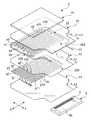
- FIG. 11is a schematic cross-sectional view of an input device 100 in the related art.
- the input device 100is a pad-type pointing device for use in notebook-type personal computers.
- an X electrode layer 103 having a plurality of X electrodes 102is formed on the upper surface of a synthetic resin film board (sensor board) 101
- a Y electrode layer 105 having a plurality of Y electrodes 104is formed on the lower surface of the film board 101 , such that the X electrodes 102 and the Y electrodes 104 are arranged into a matrix.
- the X electrode layer 103 and the Y electrode layer 105are covered with insulating films 106 and 107 , respectively.
- a top sheet 108is provided above the X electrode layer 103 serving as a sensing surface.
- the electrode layers 103 and 105 , the insulating films 106 and 107 , and the top sheet 108are rectangular with the same dimension.
- the input device 100further includes a control circuit board 110 on the bottom layer opposite to the top sheet 108 .
- the control circuit board 110is also rectangular with the same dimension as the film board 101 .
- a control circuit 111is formed on a surface of the control circuit board 110 that is farthest from the film board 101 .
- through-holesare formed in the film board 101 , the insulating film 107 , and the control circuit board 110 . This allows the X electrode layer 103 and the Y electrode layer 105 to be electrically connected with each other so that a signal in response to capacitance detected between the X electrode layer 103 and the Y electrode layer 105 is passed to the control circuit 111 .
- the electrode layers 103 and 105 , and the film board 101overlie the control circuit board 110 , thus making the related art input device 100 thick.
- a notebook-type personal computer (PC) incorporating such a thick input device 100cannot be thin.
- the control circuit board 110has the same size and area as the film board 101 , leading to increased cost.
- the present inventionprovides an input device.
- the input deviceincludes a sensor board, an X electrode layer having electrodes, a Y electrode layer having electrodes, and an insulating film disposed between the X and Y electrode layers.
- the X electrode layer and the Y electrode layerare disposed proximate to each other and on one surface of the sensor board.
- through-holesmay be formed in the insulating film. Ends of the electrodes in one of the X electrode layer and the Y electrode layer may be led through the through-holes onto the same plane as ends of the electrodes in the other layer, and the ends of the electrodes in the X and Y electrode layers may oppose and be directly connected to a conductor portion on a control circuit board.
- control circuit boardthere is no need to dispose a control circuit board beneath the sensor board, thus making the input device thin.
- the control circuit boardcan be compact, thus reducing cost.
- the through-holesare formed so as to correspond to portions of the X electrode layer or the Y electrode layer.
- an extending portion of the sensor board, in which one electrode layer is led to the same plane as the other electrode layer,can be reduced.
- a dummy electrodemay be formed between adjacent electrodes in the X electrode layer so as to be parallel to the X electrode layer, and a dummy electrode may be formed between adjacent electrodes in the Y electrode layer so as to be parallel to the Y electrode layer.
- the sensor boardmay comprise a film board, thus making the input device thin.
- the sensor board and the control circuit boardare bonded to each other by a heated, pressurized thermosetting adhesive such that the ends of the electrodes in the X and Y electrode layers on the sensor board contact the conductor portion on the control circuit board.
- a holemay be formed in the conductor portion so as to pass through the control circuit board, the hole being connected to the conductor portion.
- the adhesivemay substantially fill the hole, thus, increasing the bonding intensity. Substantially no adhesive may be present between the ends of the electrodes in the X and Y electrode layers on the sensor board and the conductor portion on the control circuit board.
- the sensor board and the insulating filmmay have extending portions that project in a direction of the plane of the sensor board and the insulating film, respectively.
- the extending portion of the sensor boardmay extend further than and overlap the extending portion of the insulating film. Ends of the electrodes in the X and Y electrode layers may be disposed on the same plane of the extending portion of the sensor board.
- a second insulating filmmay oppose the first insulating film with one of the X and Y electrode layers disposed therebetween.
- a top sheet that is contactable by the usermay be disposed on the sensor board.
- the connector portionmay comprise a planar array of land portions separated by gaps with adhesive disposed in the gaps.
- the input devicecomprises a sensor board, X and Y electrode layers each having electrodes, the X electrode and Y electrode layers disposed proximate to each other, and an insulating film disposed between the X and Y electrode layers. Ends of the electrodes in the X and Y electrode layers are disposed on the same plane of the sensor board.
- the sensor board and the insulating filmmay have extending portions that project in a direction of the plane of the sensor board and the insulating film, respectively, the extending portion of the sensor board extending further than and overlapping the extending portion of the insulating film, the ends of the electrodes in the X and Y electrode layers disposed on the extending portion of the sensor board.
- the input devicemay further comprise a control circuit board having a conductor portion, the ends of the electrodes in the X and Y electrode layers oppose and directly connected to the conductor portion.
- Through-holesmay be formed in the insulating film, the ends of the electrodes in one of the X electrode layer and the Y electrode layer led through the through-holes onto the extending portion of the sensor board.
- the through-holesmay correspond to portions of one of the X electrode layer and the Y electrode layer.
- the sensor board and the control circuit boardmay be bonded to each other by an adhesive. Substantially no adhesive may be present between the ends of the electrodes in the X and Y electrode layers on the sensor board and the conductor portion on the control circuit board.
- a holemay be formed in the conductor portion that passes through the control circuit board with the hole connected to the conductor portion and the adhesive substantially filling the hole.
- the connector portionmay comprise a planar array of land portions separated by gaps and the adhesive disposed in the gaps.
- a first and second dummy electrodemay be formed between adjacent electrodes in the X and Y electrode layers, respectively, such that the first and second dummy electrodes are parallel to the adjacent electrodes in the X and Y electrode layers, respectively.
- a top sheetmay be disposed on the sensor board that is contactable by a user. The entirety of the X and Y electrode layers may be disposed on the same side of the sensor board.
- a method of decreasing a thickness of a capacitive input devicecomprises separating X and Y electrode layers by an insulating film such that the X and Y electrode layers are disposed proximate to each other and combining ends of electrodes in the X and Y electrode layers on the same plane of a sensor board.
- the methodmay further comprise extending a portion of the sensor board and the insulating film in parallel directions, the extending portion of the sensor board extending further than the extending portion of the insulating film and combining the ends of the electrodes in the X and Y electrode layers on the extending portion of the sensor board.
- the methodmay further comprise directly connecting a conductor portion of a control circuit board to the ends of the electrodes in the X and Y electrode layers.
- the methodmay further comprise guiding the ends of the electrodes in one of the X electrode layer and the Y electrode layer through through-holes to merge the ends of electrodes in the X and Y electrode layers on the same plane of the sensor board.
- the methodmay further comprise bonding the sensor board and the control circuit board by an adhesive and substantially eliminating adhesive from between the ends of the electrodes in the X and Y electrode layers on the sensor board and the conductor portion on the control circuit board.
- the methodmay further comprise substantially filling a hole formed in the conductor portion, and that passes through the control circuit board, with the adhesive.
- the methodmay further comprise heating and pressurizing thermosetting adhesive to bond the sensor board and the control circuit board to each other.
- the methodmay further comprise bonding the sensor board and the control circuit board using adhesive disposed in gaps separating a planar array of land portions that form the connector portion.
- the methodmay further comprise decreasing adverse effects of external environmental problems by forming dummy electrodes between adjacent electrodes in the X and Y electrode layers, respectively, that are parallel to the adjacent electrodes in the X and Y electrode layers.
- the methodmay further comprise placing a top sheet on the sensor board such that when the top sheet is contacted by a user, a variation in capacitance between the electrodes in the X and Y electrode layers is detectable.
- an input device according to the present inventioncan be thinner than an input device in the related art, thus allowing a notebook computer incorporating the input device according to the present invention to be thinner. Furthermore, a control circuit substrate according to the present invention can be more compact than a control circuit substrate in the related art, and does not require multilayer substrate such as a four-layer substrate, thus achieving cost reduction.
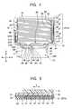
- FIG. 1is an exploded perspective view of an input device according to the present invention
- FIG. 2is a circuit diagram of an X electrode layer
- FIG. 3is a plan view of through-holes formed in an insulating film
- FIG. 4is a circuit diagram of a Y electrode layer
- FIG. 5is a cross-sectional view of a portion of the input device, taken along the X direction;
- FIG. 6is a cross-sectional view of a portion of the input device, taken along the Y direction;
- FIG. 7is a cross-sectional view of a portion of the input device, taken along a plane passing through connections between the X electrode layer and the Y electrode layer;
- FIG. 8is a plan view of a conductor portion formed on a control circuit substrate
- FIG. 9is a plan view showing that the control circuit substrate and the electrode layers are bonded to each other;
- FIG. 10is a cross-sectional view of the bonded product, taken along a line X-X of FIG. 9;
- FIG. 11is a schematic cross-sectional view of an input device in the related art.
- FIG. 1is an exploded perspective view of an input device 1 according to the present invention
- FIG. 2is a circuit diagram of an X electrode layer
- FIG. 3is a plan view of through-holes formed in an insulating film
- FIG. 4is a circuit diagram of a Y electrode layer
- FIG. 5is a cross-sectional view of a portion of the input device 1 , taken along the X direction
- FIG. 6is a cross-sectional view of a portion of the input device 1 , taken along the Y direction
- FIG. 7is a cross-sectional view of a portion of the input device 1 , taken along a plane passing through connections between the X electrode layer and the Y electrode layer.
- the input device 1 shown in FIG. 1includes a film board 10 serving as a sensor board in the present invention.
- the film board 10is formed of a sheet made of a synthetic resin having an insulating property, such as PET (polyethylene terephthalate). As shown in FIG. 1, a portion of the film board 10 extends sideward from one longer side thereof to form an extending portion 11 .
- An X electrode layer 20 Xis provided on the lower surface of the film board 10 .
- the X electrode layer 20 Xincludes an X driving electrode array 20 Xd having a plurality of ( 16 in this example) X electrodes x 1 , x 2 , . . . , x 15 , and x 16 arranged in the X direction at predetermined intervals and in parallel to each other.
- An end of each of the X electrodes x 1 , x 2 , . . . , x 15 , and x 16extends to the extending portion 11 .
- the X electrode layer 20 X formed on the film board 10further includes a total of 15 dummy electrodes xd which are alternated with the X electrodes x 1 , x 2 , . . . , x 15 , and x 16 so that each dummy electrode xd is formed between adjacent X electrodes.
- the dummy electrodes xdreduce adverse effect caused by defects on the X and Y electrode layers or external environmental problems, for example, water droplets placed on a surface of the input device 1 .
- a ground electrode 21is further formed on the film board 10 , in the same plane as the X driving electrode array 20 Xd, so as to extend to the extending portion 11 along the periphery of the film board 10 .
- X switching electrode arrays 22 , 23 , and 24each having a plurality of electrodes are formed in spaces between the X driving electrode array 20 Xd and the ground electrode 21 .
- the X driving electrode array 20 Xd, the ground electrode 21 , and the X switching electrode arrays 22 , 23 , and 24are produced using silver paste or silver-based paste by screen printing.
- An insulating film 12 having an insulating resin (resist) applied or printed thereonis provided over surfaces of the X driving electrode array 20 Xd, the ground electrode 21 , and the X switching electrode arrays 22 , 23 , and 24 .
- resists used hereininclude polyamide resins, epoxy resins, polyurethane resins, and polyester resins.
- a plurality of through-holes h 1 , h 2 , . . . , h 12 , k 2 , k 4 , . . . , k 10 , m 2 , m 4 , . . . , m 10 , and s 2are formed in the insulating film 12 , as shown in FIG. 3.
- the through-holesare formed so as to meet ends of the electrodes in the X switching electrode arrays 22 , 23 , and 24 .
- the electrodes shown in FIG. 2which do not correspond to the through-holes shown in FIG. 3 are test
- a Y electrode layer 20 Yis provided on a surface (lower surface) of the insulating film 12 .
- the Y electrode layer 20 Yincludes a Y driving electrode array 20 Yd having a plurality of ( 12 in this example) Y electrodes y 1 , y 2 , . . . , y 11 , and y 12 arranged in a direction orthogonal to the X driving electrode array 20 Xd. Some of the Y electrodes y 1 , y 2 , . . .
- the electrodes y 1 , y 3 , y 5 , y 7 , y 9 , and y 11each have one end extending to some of the through-holes shown in FIG. 3 along the left and right sides (in the X direction).
- a sensor electrode Sis provided on the surface (lower surface) of the insulating film 12 in the same layer as the Y driving electrode array 20 Yd.
- the sensor electrode Sis formed of comb-like electrode arrays sa and sb each having electrodes ys.
- the electrodes ys in the comb-like electrode arrays sa and sbare interleaved with the Y electrodes y 1 , y 2 , . . . , y 11 , and y 12 .
- the comb-like electrode array sais horizontally reversed with respect to the comb-like electrode array sb in such a manner that the tip of the comb-like electrode array sa opposes the tip of the comb-like electrode array sb.
- the comb-like electrode arrays sa and sbare combined into a single electrode at the center in the Y direction, extending to the through-hole shown in FIG. 3.
- the electrodes in the X electrode layer 20 Xare indicated by outlined thick lines, while, in FIG. 4, the electrodes in the Y electrode layer 20 Y are indicated by thin solid lines. However, both electrode arrays are formed of electrodes having substantially the same width.
- an insulating film 13similar to the insulating film 12 , which is made of an insulating resin is formed over a surface including the Y driving electrode array 20 Yd by printing.
- a top sheet 14which is touched by a finger of a user or a pen operated by a user (in other words contactable by a user), is secured to the upper surface of the film board 10 by an adhesive or the like.
- the Y electrodes y 1 , y 3 , y 5 , y 7 , y 9 , and y 11extend to contacts b 1 , b 3 , b 5 , b 7 , b 9 , and b 11 , respectively.
- the Y electrodes y 1 , y 3 , y 5 , y 7 , y 9 , and y 11are connected to contacts a 1 , a 3 , a 5 , a 7 , a 9 , and all provided for the X switching electrode array 24 via the through-holes h 1 , h 3 , h 5 , h 7 , h 9 , and h 11 , respectively.
- the X switching electrode array 22is provided with contacts c 2 , c 4 , and c 6 at the electrode ends opposite to the contacts a 2 , a 4 , and a 6 .
- the X switching electrode array 23is provided with contacts c 8 and c 10 at the electrode ends opposite to the contacts a 8 and a 10 .
- the contacts c 2 , c 4 , c 6 , c 8 , and c 10are connected to contacts d 2 , d 4 , d 6 , d 8 , and d 10 provided for electrode ends of a Y switching electrode array 26 via the through-holes k 2 , k 4 , k 6 , k 8 , and k 10 formed in the insulating film 12 , respectively.
- the Y switching electrode array 26is further provided with contacts e 2 , e 4 , e 6 , e 8 , and e 10 at the electrode ends opposite to the contacts d 2 , d 4 , d 6 , d 8 , and d 10 .
- the contacts e 2 , e 4 , e 6 , e 8 , and e 10are connected to contacts f 2 , f 4 , f 6 , f 8 , and f 10 provided for the X switching electrode array 24 via the through-holes m 2 , m 4 , m 6 , m 8 , and m 10 formed in the insulating film 12 , respectively.
- the Y electrodes y 2 , y 4 , y 6 , y 8 , y 10 , and y 12are led from the Y electrode layer 20 Y onto the same plane as the X electrode layer 20 X.
- a contact s 1 extending from the sensor electrode S formed in the Y electrode layer 20 Yis connected to a contact s 3 for the X switching electrode array 24 via the through-hole s 2 formed in the insulating film 12 .
- the thus configured circuitallows all of the electrodes in the X electrode layer 20 X and the Y electrode layer 20 Y to be gathered to an edge portion Ds of the extending portion 11 on the film board 10 .
- the film board 10is placed so as to project from the left and right sides of the top sheet 14 in the X direction. Further referring to FIG. 6, one longer side of the top sheet 14 is aligned with the longer side of the film board 10 . Therefore, the left and right sides of the film board 10 , and the extending portion 11 project with respect to the top sheet 14 when the input device 1 is viewed from above the top sheet 14 .
- the Y electrodes y 1 , y 3 , etc.pass across the surface of the insulating film 12 , and are connected to the X switching electrode array 24 in the X electrode layer 20 X via the through-holes h 1 , h 3 , etc. . . .
- the circuit patterns of the Y electrodes y 1 , y 2 , . . . , y 11 , and y 12are separately formed on the upper and lower surfaces of the insulating film 12 , thus making the pitch between electrodes narrower. If the electrodes on the upper surface of the insulating film 12 overlap the electrodes on the lower surface of the insulating film 12 , there is no electrical connection therebetween. Therefore, the portions of the film board 10 which project beyond the top sheet 14 can be reduced in dimension. Thus, the overall input device 1 can be compact.
- the leading ends (hereinafter referred to as “Ds ends”) of all electrodes in the X electrode layer 20 X and all electrodes in the Y electrode layer 20 Yare introduced to the edge portion Ds of the extending portion 11 provided for the film board 10 .
- the dimension by which the extending portion 11 projects (L 1 +L 2 )is greater than the dimension by which the insulating films 12 and 13 project so as to overlap the extending portion 11 (L 2 ).
- the Ds ends of electrodes in the X and Y electrode layers 20 X and 20 Y formed on the film board 10are exposed on the surface (lower surface) of the film board 10 (see FIG. 1).
- the Ds ends of electrodes in the X electrode layer 20 X and the Y electrode layer 20 Yare connected to a conductor portion 5 formed on the control circuit substrate 4 .
- the control circuit substrate 4is much smaller than the film board 10 .
- a region having dimension L, as shown in FIG. 2, which is exposedis connected to the conductor portion 5 .
- the control circuit substrate 4is formed of a board 4 a made of paper phenol, paper epoxy, glass epoxy or the like, and the conductor portion 5 connected to the Ds ends of electrodes in the X and Y electrode layers 20 X and 20 Y is formed on one surface of the board 4 a .
- the conductor portion 5includes a plurality of lands 5 a arranged at predetermined intervals in the X direction.
- the conductor portion 5may be formed of a metal foil such as a copper foil.
- the metal foilmay be plated with gold or coated with carbon. Preferably, the gold plating is used in view of resistance or bonding intensity.
- Each of the lands 5 a on the control circuit substrate 4is divided into land portions 5 a 1 and 5 a 2 by a minute gap Sb.
- Land portions 7 a 1 and 7 a 2having a similar pattern to the land portions 5 a 1 and 5 a 2 of the conductor portion 5 are formed on the opposite surface of the control circuit substrate 4 (see FIG. 10).
- the land portions 5 a 1 and 5 a 2have holes 6 a and 6 b formed therein which reach the land portions 7 a 1 and 7 a 2 , respectively.
- the circuit pattern of the land portions 7 a 1extends around the control circuit substrate 4 so that the land portions 7 a 1 are connected to a control circuit 8 , etc., mounted on the board 4 a .
- the land portions 5 a 2 and 7 a 2serve as test circuits.
- the Ds ends of electrode in the electrode layers 20 X and 20 Yare bonded to the control circuit substrate 4 by applying a thermosetting adhesive 30 (depicted as hatched in FIG. 8) in a line to the gaps 5 b formed in the conductor portion 5 .
- the adhesive 30is made of an insulating fluid material, such as an epoxy resin, which contains no conductive particles.
- FIG. 9illustrates the bonded product
- FIG. 10is a cross-sectional view of the product, taken along a line X-X of FIG. 9.
- the adhesive 30expands and enters the spaces 5 c and 5 d , thus ensuring that the film board 10 is bonded to the control circuit substrate 4 .
- the pressurizationallows the adhesive 30 to be substantially eliminated from bonding surfaces T between the electrodes in the edge portion Ds and the land portions 5 a 1 and 5 a 2 of the conductor portion 5 .
- the Ds ends of electrodes in the X and Y electrode layers 20 X and 20 Ycan be directly and electrically connected to the conductor portion 5 , as shown in FIG. 10.
- FIG. 10As shown in FIG.
- the Ds ends of electrodes in the X and Y electrode layers 20 X and 20 Yare disposed on the same plane on the extending portion 11 of the sensor board 10 and the insulating films 12 and 13 are not present between the conductor portion 5 of the control board 4 and the Ds ends of electrodes in the X and Y electrode layers 20 X and 20 Y, thereby decreasing the thickness of the composite.
- the adhesive 30 applied to the surfaces of the land portions 5 a 1 and 5 a 2also enters the holes 6 a and 6 b from the surfaces of the land portions 5 a 1 and 5 a 2 .
- the adhesive 30substantially fills in the holes 6 a and 6 b and is hardened therein, thereby increasing the bonding intensity between the control circuit substrate 4 and the edge portion Ds.
- a dummy conductormay be provided in the vicinity of the conductor portion 5 on the control circuit substrate 4 , and a dummy electrode may also be provided on the film board 10 so as to overlap the dummy conductor, thus further increasing the bonding intensity.
- touchis sensed by the X driving electrode array 20 Xd, the Y driving electrode 20 Yd, and the sensor electrode S.
- the X driving electrode array 20 Xdis selected every two X electrodes to obtain a detection output corresponding to a variation of capacitance between the X driving electrode array 20 Xd and the sensor electrode S.
- the Y driving electrode array 20 Ydis selected every two Y electrodes to obtain a detection output corresponding to a variation of capacitance between the Y driving electrode array 20 Yd and the sensor electrode S.
- the X and Y electrode layersare disposed proximate to each other.
- Proximate to each other in this casemeans that the X and Y electrode layers are disposed close enough together to permit this variation in capacitance to be detected using conventional detection techniques that detect the change of capacitance in existing capacitive input sensors, for example.
- the detection outputs from all electrodes in the X driving electrode array 20 Xd and the detection outputs from all electrodes in the Y driving electrode array 20 Ydare alternately obtained in a time-division manner.
- the thus obtained detection outputsare amplified by an amplifier, and are converted into digital signals by an analog-to-digital (A/D) converter.
- a control unitperforms a predetermined calculation on the digital signals, and sends the resulting signals to a personal computer (PC), where the signals are controlled according to the calculation result.
- PCpersonal computer
Landscapes
- Engineering & Computer Science (AREA)
- General Engineering & Computer Science (AREA)
- Theoretical Computer Science (AREA)
- Human Computer Interaction (AREA)
- Physics & Mathematics (AREA)
- General Physics & Mathematics (AREA)
- Position Input By Displaying (AREA)
Abstract
Description
- 1. Field of the Invention[0001]
- The present invention relates to a capacitive input device used as, for example, a pointing device for a personal computer.[0002]
- 2. Description of the Related Art[0003]
- FIG. 11 is a schematic cross-sectional view of an[0004]
input device 100 in the related art. Theinput device 100 is a pad-type pointing device for use in notebook-type personal computers. - In the[0005]
input device 100 shown in FIG. 11, anX electrode layer 103 having a plurality ofX electrodes 102 is formed on the upper surface of a synthetic resin film board (sensor board)101, and aY electrode layer 105 having a plurality ofY electrodes 104 is formed on the lower surface of thefilm board 101, such that theX electrodes 102 and theY electrodes 104 are arranged into a matrix. TheX electrode layer 103 and theY electrode layer 105 are covered withinsulating films top sheet 108 is provided above theX electrode layer 103 serving as a sensing surface. Theelectrode layers insulating films top sheet 108 are rectangular with the same dimension. - The[0006]
input device 100 further includes acontrol circuit board 110 on the bottom layer opposite to thetop sheet 108. Thecontrol circuit board 110 is also rectangular with the same dimension as thefilm board 101. Acontrol circuit 111 is formed on a surface of thecontrol circuit board 110 that is farthest from thefilm board 101. - In the[0007]
input device 100, through-holes (not shown) are formed in thefilm board 101, theinsulating film 107, and thecontrol circuit board 110. This allows theX electrode layer 103 and theY electrode layer 105 to be electrically connected with each other so that a signal in response to capacitance detected between theX electrode layer 103 and theY electrode layer 105 is passed to thecontrol circuit 111. - However, the[0008]
electrode layers film board 101 overlie thecontrol circuit board 110, thus making the relatedart input device 100 thick. A notebook-type personal computer (PC) incorporating such athick input device 100 cannot be thin. Moreover, thecontrol circuit board 110 has the same size and area as thefilm board 101, leading to increased cost. - In order to solve the above-described problems, it is an object of the present invention to provide a thin and low-cost input device.[0009]
- The present invention provides an input device. The input device includes a sensor board, an X electrode layer having electrodes, a Y electrode layer having electrodes, and an insulating film disposed between the X and Y electrode layers. The X electrode layer and the Y electrode layer are disposed proximate to each other and on one surface of the sensor board.[0010]
- In the above input device, through-holes may be formed in the insulating film. Ends of the electrodes in one of the X electrode layer and the Y electrode layer may be led through the through-holes onto the same plane as ends of the electrodes in the other layer, and the ends of the electrodes in the X and Y electrode layers may oppose and be directly connected to a conductor portion on a control circuit board.[0011]
- According to the present invention, there is no need to dispose a control circuit board beneath the sensor board, thus making the input device thin. The control circuit board can be compact, thus reducing cost.[0012]
- Preferably, the through-holes are formed so as to correspond to portions of the X electrode layer or the Y electrode layer. Thus, an extending portion of the sensor board, in which one electrode layer is led to the same plane as the other electrode layer, can be reduced.[0013]
- A dummy electrode may be formed between adjacent electrodes in the X electrode layer so as to be parallel to the X electrode layer, and a dummy electrode may be formed between adjacent electrodes in the Y electrode layer so as to be parallel to the Y electrode layer.[0014]
- The sensor board may comprise a film board, thus making the input device thin.[0015]
- Preferably, the sensor board and the control circuit board are bonded to each other by a heated, pressurized thermosetting adhesive such that the ends of the electrodes in the X and Y electrode layers on the sensor board contact the conductor portion on the control circuit board.[0016]
- A hole may be formed in the conductor portion so as to pass through the control circuit board, the hole being connected to the conductor portion. The adhesive may substantially fill the hole, thus, increasing the bonding intensity. Substantially no adhesive may be present between the ends of the electrodes in the X and Y electrode layers on the sensor board and the conductor portion on the control circuit board.[0017]
- The sensor board and the insulating film may have extending portions that project in a direction of the plane of the sensor board and the insulating film, respectively. The extending portion of the sensor board may extend further than and overlap the extending portion of the insulating film. Ends of the electrodes in the X and Y electrode layers may be disposed on the same plane of the extending portion of the sensor board.[0018]
- A second insulating film may oppose the first insulating film with one of the X and Y electrode layers disposed therebetween. A top sheet that is contactable by the user may be disposed on the sensor board.[0019]
- The connector portion may comprise a planar array of land portions separated by gaps with adhesive disposed in the gaps.[0020]
- In another embodiment, the input device comprises a sensor board, X and Y electrode layers each having electrodes, the X electrode and Y electrode layers disposed proximate to each other, and an insulating film disposed between the X and Y electrode layers. Ends of the electrodes in the X and Y electrode layers are disposed on the same plane of the sensor board.[0021]
- The sensor board and the insulating film may have extending portions that project in a direction of the plane of the sensor board and the insulating film, respectively, the extending portion of the sensor board extending further than and overlapping the extending portion of the insulating film, the ends of the electrodes in the X and Y electrode layers disposed on the extending portion of the sensor board.[0022]
- The input device may further comprise a control circuit board having a conductor portion, the ends of the electrodes in the X and Y electrode layers oppose and directly connected to the conductor portion. Through-holes may be formed in the insulating film, the ends of the electrodes in one of the X electrode layer and the Y electrode layer led through the through-holes onto the extending portion of the sensor board. The through-holes may correspond to portions of one of the X electrode layer and the Y electrode layer.[0023]
- The sensor board and the control circuit board may be bonded to each other by an adhesive. Substantially no adhesive may be present between the ends of the electrodes in the X and Y electrode layers on the sensor board and the conductor portion on the control circuit board. A hole may be formed in the conductor portion that passes through the control circuit board with the hole connected to the conductor portion and the adhesive substantially filling the hole. The connector portion may comprise a planar array of land portions separated by gaps and the adhesive disposed in the gaps.[0024]
- A first and second dummy electrode may be formed between adjacent electrodes in the X and Y electrode layers, respectively, such that the first and second dummy electrodes are parallel to the adjacent electrodes in the X and Y electrode layers, respectively. A top sheet may be disposed on the sensor board that is contactable by a user. The entirety of the X and Y electrode layers may be disposed on the same side of the sensor board.[0025]
- In another embodiment, a method of decreasing a thickness of a capacitive input device comprises separating X and Y electrode layers by an insulating film such that the X and Y electrode layers are disposed proximate to each other and combining ends of electrodes in the X and Y electrode layers on the same plane of a sensor board.[0026]
- The method may further comprise extending a portion of the sensor board and the insulating film in parallel directions, the extending portion of the sensor board extending further than the extending portion of the insulating film and combining the ends of the electrodes in the X and Y electrode layers on the extending portion of the sensor board.[0027]
- The method may further comprise directly connecting a conductor portion of a control circuit board to the ends of the electrodes in the X and Y electrode layers.[0028]
- The method may further comprise guiding the ends of the electrodes in one of the X electrode layer and the Y electrode layer through through-holes to merge the ends of electrodes in the X and Y electrode layers on the same plane of the sensor board.[0029]
- The method may further comprise bonding the sensor board and the control circuit board by an adhesive and substantially eliminating adhesive from between the ends of the electrodes in the X and Y electrode layers on the sensor board and the conductor portion on the control circuit board.[0030]
- The method may further comprise substantially filling a hole formed in the conductor portion, and that passes through the control circuit board, with the adhesive.[0031]
- The method may further comprise heating and pressurizing thermosetting adhesive to bond the sensor board and the control circuit board to each other.[0032]
- The method may further comprise bonding the sensor board and the control circuit board using adhesive disposed in gaps separating a planar array of land portions that form the connector portion.[0033]
- The method may further comprise decreasing adverse effects of external environmental problems by forming dummy electrodes between adjacent electrodes in the X and Y electrode layers, respectively, that are parallel to the adjacent electrodes in the X and Y electrode layers.[0034]
- The method may further comprise placing a top sheet on the sensor board such that when the top sheet is contacted by a user, a variation in capacitance between the electrodes in the X and Y electrode layers is detectable.[0035]
- Therefore, an input device according to the present invention can be thinner than an input device in the related art, thus allowing a notebook computer incorporating the input device according to the present invention to be thinner. Furthermore, a control circuit substrate according to the present invention can be more compact than a control circuit substrate in the related art, and does not require multilayer substrate such as a four-layer substrate, thus achieving cost reduction.[0036]
- FIG. 1 is an exploded perspective view of an input device according to the present invention;[0037]
- FIG. 2 is a circuit diagram of an X electrode layer;[0038]
- FIG. 3 is a plan view of through-holes formed in an insulating film;[0039]
- FIG. 4 is a circuit diagram of a Y electrode layer;[0040]
- FIG. 5 is a cross-sectional view of a portion of the input device, taken along the X direction;[0041]
- FIG. 6 is a cross-sectional view of a portion of the input device, taken along the Y direction;[0042]
- FIG. 7 is a cross-sectional view of a portion of the input device, taken along a plane passing through connections between the X electrode layer and the Y electrode layer;[0043]
- FIG. 8 is a plan view of a conductor portion formed on a control circuit substrate;[0044]
- FIG. 9 is a plan view showing that the control circuit substrate and the electrode layers are bonded to each other;[0045]
- FIG. 10 is a cross-sectional view of the bonded product, taken along a line X-X of FIG. 9; and[0046]
- FIG. 11 is a schematic cross-sectional view of an input device in the related art.[0047]
- FIG. 1 is an exploded perspective view of an[0048]
input device 1 according to the present invention; FIG. 2 is a circuit diagram of an X electrode layer; FIG. 3 is a plan view of through-holes formed in an insulating film; FIG. 4 is a circuit diagram of a Y electrode layer; FIG. 5 is a cross-sectional view of a portion of theinput device 1, taken along the X direction; FIG. 6 is a cross-sectional view of a portion of theinput device 1, taken along the Y direction; and FIG. 7 is a cross-sectional view of a portion of theinput device 1, taken along a plane passing through connections between the X electrode layer and the Y electrode layer. - The[0049]
input device 1 shown in FIG. 1 includes afilm board 10 serving as a sensor board in the present invention. Thefilm board 10 is formed of a sheet made of a synthetic resin having an insulating property, such as PET (polyethylene terephthalate). As shown in FIG. 1, a portion of thefilm board 10 extends sideward from one longer side thereof to form an extendingportion 11. - An[0050]
X electrode layer 20X is provided on the lower surface of thefilm board 10. As shown in FIG. 2, theX electrode layer 20X includes an X driving electrode array20Xd having a plurality of (16 in this example) X electrodes x1, x2, . . . , x15, and x16 arranged in the X direction at predetermined intervals and in parallel to each other. An end of each of the X electrodes x1, x2, . . . , x15, and x16 extends to the extendingportion 11. - The[0051]
X electrode layer 20X formed on thefilm board 10 further includes a total of 15 dummy electrodes xd which are alternated with the X electrodes x1, x2, . . . , x15, and x16 so that each dummy electrode xd is formed between adjacent X electrodes. The dummy electrodes xd reduce adverse effect caused by defects on the X and Y electrode layers or external environmental problems, for example, water droplets placed on a surface of theinput device 1. - A[0052]
ground electrode 21 is further formed on thefilm board 10, in the same plane as the X driving electrode array20Xd, so as to extend to the extendingportion 11 along the periphery of thefilm board 10. On thefilm board 10, X switchingelectrode arrays ground electrode 21. The X driving electrode array20Xd, theground electrode 21, and the X switchingelectrode arrays - For brevity, certain materials used as the various electrodes, arrays and connecters have been described. However, this is not to say that the present invention is limited to these materials. This is to say that metallic pastes and other conductive materials, including nonmetallic conductors, may be used to produce the various electrodes, arrays and conductive connecters described herein. The processes for producing and using these conductive materials are generally well known in the art.[0053]
- An insulating[0054]
film 12 having an insulating resin (resist) applied or printed thereon is provided over surfaces of the X driving electrode array20Xd, theground electrode 21, and the X switchingelectrode arrays film 12, as shown in FIG. 3. The through-holes are formed so as to meet ends of the electrodes in the X switchingelectrode arrays - Referring to FIG. 4, a[0055]
Y electrode layer 20Y is provided on a surface (lower surface) of the insulatingfilm 12. TheY electrode layer 20Y includes a Y driving electrode array20Yd having a plurality of (12 in this example) Y electrodes y1, y2, . . . , y11, and y12 arranged in a direction orthogonal to the X driving electrode array20Xd. Some of the Y electrodes y1, y2, . . . , y11, and y12, namely, the electrodes y1, y3, y5, y7, y9, and y11, each have one end extending to some of the through-holes shown in FIG. 3 along the left and right sides (in the X direction). - A sensor electrode S is provided on the surface (lower surface) of the insulating[0056]
film 12 in the same layer as the Y driving electrode array20Yd. The sensor electrode S is formed of comb-like electrode arrays sa and sb each having electrodes ys. The electrodes ys in the comb-like electrode arrays sa and sb are interleaved with the Y electrodes y1, y2, . . . , y11, and y12. The comb-like electrode array sa is horizontally reversed with respect to the comb-like electrode array sb in such a manner that the tip of the comb-like electrode array sa opposes the tip of the comb-like electrode array sb. The comb-like electrode arrays sa and sb are combined into a single electrode at the center in the Y direction, extending to the through-hole shown in FIG. 3. - In FIG. 2, the electrodes in the[0057]
X electrode layer 20X are indicated by outlined thick lines, while, in FIG. 4, the electrodes in theY electrode layer 20Y are indicated by thin solid lines. However, both electrode arrays are formed of electrodes having substantially the same width. - As shown in FIG. 1, an insulating[0058]
film 13, similar to the insulatingfilm 12, which is made of an insulating resin is formed over a surface including the Y driving electrode array20Yd by printing. Atop sheet 14, which is touched by a finger of a user or a pen operated by a user (in other words contactable by a user), is secured to the upper surface of thefilm board 10 by an adhesive or the like. - When the[0059]
X electrode layer 20X and theY electrode layer 20Y are formed on one side of thefilm board 10 in the aforementioned manner, the electrodes in theY electrode layer 20Y must be led to the plane in which theX electrode layer 20X is formed. A formation process for electrodes in the illustrated embodiment is now described with reference to FIGS.2 to4. - In the[0060]
Y electrode layer 20Y, the Y electrodes y1, y3, y5, y7, y9, and y11 extend to contacts b1, b3, b5, b7, b9, and b11, respectively. The Y electrodes y1, y3, y5, y7, y9, and y11 are connected to contacts a1, a3, a5, a7, a9, and all provided for the X switchingelectrode array 24 via the through-holes h1, h3, h5, h7, h9, and h11, respectively. - Contacts b[0061]2, b4, b6, b8, b10, and b12 at the ends of the Y electrodes y2, y4, y6, y8, y10, and y12 are connected to contacts a2, a4, and a6 at the electrode ends of the X switching
electrode array 22, and contacts a8, a10, and a12 at the electrode ends of the X switchingelectrode array 23 via the through-holes h2, h4, h6, h8, h10, and h12 formed in the insulatingfilm 12, respectively. Only the electrode provided with the contact a12 extends to the edge of the extendingportion 11. The Xswitching electrode array 22 is provided with contacts c2, c4, and c6 at the electrode ends opposite to the contacts a2, a4, and a6. The Xswitching electrode array 23 is provided with contacts c8 and c10 at the electrode ends opposite to the contacts a8 and a10. The contacts c2, c4, c6, c8, and c10 are connected to contacts d2, d4, d6, d8, and d10 provided for electrode ends of a Y switchingelectrode array 26 via the through-holes k2, k4, k6, k8, and k10 formed in the insulatingfilm 12, respectively. The Y switchingelectrode array 26 is further provided with contacts e2, e4, e6, e8, and e10 at the electrode ends opposite to the contacts d2, d4, d6, d8, and d10. The contacts e2, e4, e6, e8, and e10 are connected to contacts f2, f4, f6, f8, and f10 provided for the X switchingelectrode array 24 via the through-holes m2, m4, m6, m8, and m10 formed in the insulatingfilm 12, respectively. Thus, the Y electrodes y2, y4, y6, y8, y10, and y12 are led from theY electrode layer 20Y onto the same plane as theX electrode layer 20X. - A contact s[0062]1 extending from the sensor electrode S formed in the
Y electrode layer 20Y is connected to a contact s3 for the X switchingelectrode array 24 via the through-hole s2 formed in the insulatingfilm 12. - The thus configured circuit allows all of the electrodes in the[0063]
X electrode layer 20X and theY electrode layer 20Y to be gathered to an edge portion Ds of the extendingportion 11 on thefilm board 10. - Referring to FIG. 5, in the[0064]
input device 1, thefilm board 10 is placed so as to project from the left and right sides of thetop sheet 14 in the X direction. Further referring to FIG. 6, one longer side of thetop sheet 14 is aligned with the longer side of thefilm board 10. Therefore, the left and right sides of thefilm board 10, and the extendingportion 11 project with respect to thetop sheet 14 when theinput device 1 is viewed from above thetop sheet 14. - At the connections between the[0065]
X electrode layer 20X and theY electrode layer 20Y via the through-holes, as shown in FIG. 7, silver or silver-based paste is filled in the through-holes h2, h4, etc., in the insulatingfilm 12 when the Y electrodes y2, y4, etc., are printed, thereby providing electrical connection with the contacts a2, a4, etc., for the X switchingelectrode array 22. On the other hand, the Y electrodes y1, y3, etc., pass across the surface of the insulatingfilm 12, and are connected to the X switchingelectrode array 24 in theX electrode layer 20X via the through-holes h1, h3, etc. . . . - In this way, the circuit patterns of the Y electrodes y[0066]1, y2, . . . , y11, and y12 are separately formed on the upper and lower surfaces of the insulating
film 12, thus making the pitch between electrodes narrower. If the electrodes on the upper surface of the insulatingfilm 12 overlap the electrodes on the lower surface of the insulatingfilm 12, there is no electrical connection therebetween. Therefore, the portions of thefilm board 10 which project beyond thetop sheet 14 can be reduced in dimension. Thus, theoverall input device 1 can be compact. - As shown in FIG. 2, in the[0067]
input device 1 in the illustrated embodiment, the leading ends (hereinafter referred to as “Ds ends”) of all electrodes in theX electrode layer 20X and all electrodes in theY electrode layer 20Y are introduced to the edge portion Ds of the extendingportion 11 provided for thefilm board 10. The dimension by which the extendingportion 11 projects (L1+L2) is greater than the dimension by which the insulatingfilms films film board 10, the Ds ends of electrodes in the X and Y electrode layers20X and20Y formed on thefilm board 10 are exposed on the surface (lower surface) of the film board10 (see FIG. 1). - The Ds ends of electrodes in the[0068]
X electrode layer 20X and theY electrode layer 20Y are connected to aconductor portion 5 formed on thecontrol circuit substrate 4. Thecontrol circuit substrate 4 is much smaller than thefilm board 10. A region having dimension L, as shown in FIG. 2, which is exposed is connected to theconductor portion 5. - The[0069]
control circuit substrate 4 is formed of aboard 4amade of paper phenol, paper epoxy, glass epoxy or the like, and theconductor portion 5 connected to the Ds ends of electrodes in the X and Y electrode layers20X and20Y is formed on one surface of theboard 4a. Theconductor portion 5 includes a plurality oflands 5aarranged at predetermined intervals in the X direction. Theconductor portion 5 may be formed of a metal foil such as a copper foil. The metal foil may be plated with gold or coated with carbon. Preferably, the gold plating is used in view of resistance or bonding intensity. - Each of the[0070]
lands 5aon thecontrol circuit substrate 4 is divided intoland portions 5a1 and5a2 by a minute gap Sb. Land portions7a1 and7a2 having a similar pattern to theland portions 5a1 and5a2 of theconductor portion 5 are formed on the opposite surface of the control circuit substrate4 (see FIG. 10). Theland portions 5a1 and5a2 haveholes holes land portions 5a1 and5a2 are electrically connected to the land portions7a1 and7a2, respectively. The circuit pattern of the land portions7a1 extends around thecontrol circuit substrate 4 so that the land portions7a1 are connected to acontrol circuit 8, etc., mounted on theboard 4a. Theland portions 5a2 and7a2 serve as test circuits. - As shown in FIG. 8, in the[0071]
input device 1 in the illustrated embodiment, the Ds ends of electrode in the electrode layers20X and20Y are bonded to thecontrol circuit substrate 4 by applying a thermosetting adhesive30 (depicted as hatched in FIG. 8) in a line to thegaps 5bformed in theconductor portion 5. The adhesive30 is made of an insulating fluid material, such as an epoxy resin, which contains no conductive particles. - After the adhesive[0072]30 is applied in a line to a region including the
gaps 5b, the Ds ends are positioned with respect to theconductor portion 5, which are then heated and pressurized. The Ds ends are thus bonded to thecontrol circuit substrate 4. FIG. 9 illustrates the bonded product, and FIG. 10 is a cross-sectional view of the product, taken along a line X-X of FIG. 9. When the adhesive30 is heated and pressurized, the adhesive30 expands out of thegaps 5bintospaces 5cbetween theland portions 5a1 andspaces 5dbetween theland portions 5a2, and therefore into the surrounding. The adhesive30 expands and enters thespaces film board 10 is bonded to thecontrol circuit substrate 4. The pressurization allows the adhesive30 to be substantially eliminated from bonding surfaces T between the electrodes in the edge portion Ds and theland portions 5a1 and5a2 of theconductor portion 5. Thus, the Ds ends of electrodes in the X and Y electrode layers20X and20Y can be directly and electrically connected to theconductor portion 5, as shown in FIG. 10. In addition, as shown in FIG. 10, the Ds ends of electrodes in the X and Y electrode layers20X and20Y are disposed on the same plane on the extendingportion 11 of thesensor board 10 and the insulatingfilms conductor portion 5 of thecontrol board 4 and the Ds ends of electrodes in the X and Y electrode layers20X and20Y, thereby decreasing the thickness of the composite. - The adhesive[0073]30 applied to the surfaces of the
land portions 5a1 and5a2 also enters theholes land portions 5a1 and5a2. The adhesive30 substantially fills in theholes control circuit substrate 4 and the edge portion Ds. A dummy conductor may be provided in the vicinity of theconductor portion 5 on thecontrol circuit substrate 4, and a dummy electrode may also be provided on thefilm board 10 so as to overlap the dummy conductor, thus further increasing the bonding intensity. - In the[0074]
input device 1 in the illustrated embodiment, touch is sensed by the X driving electrode array20Xd, the Y driving electrode20Yd, and the sensor electrode S. - Specifically, when a conductor such as a human finger touches the[0075]
top sheet 14 in the state where an electric field having a predetermined potential is applied between the X driving electrode array20Xd (the X electrodes x1 to x16) and the Y driving electrode array20Yd (the Y electrodes y1 to y12), capacitance between the X driving electrode array20Xd and the Y driving electrode array20Yd varies at the location which the conductor touches. - In order to obtain X-coordinate data, the X driving electrode array[0076]20Xd is selected every two X electrodes to obtain a detection output corresponding to a variation of capacitance between the X driving electrode array20Xd and the sensor electrode S. Likewise, in order to obtain Y-coordinate data, the Y driving electrode array20Yd is selected every two Y electrodes to obtain a detection output corresponding to a variation of capacitance between the Y driving electrode array20Yd and the sensor electrode S. The X and Y electrode layers are disposed proximate to each other. Proximate to each other in this case means that the X and Y electrode layers are disposed close enough together to permit this variation in capacitance to be detected using conventional detection techniques that detect the change of capacitance in existing capacitive input sensors, for example. The detection outputs from all electrodes in the X driving electrode array20Xd and the detection outputs from all electrodes in the Y driving electrode array20Yd are alternately obtained in a time-division manner.
- The thus obtained detection outputs are amplified by an amplifier, and are converted into digital signals by an analog-to-digital (A/D) converter. A control unit performs a predetermined calculation on the digital signals, and sends the resulting signals to a personal computer (PC), where the signals are controlled according to the calculation result.[0077]
Claims (38)
1. An input device comprising a sensor board, an X electrode layer having electrodes, a Y electrode layer having electrodes, and an insulating film disposed between the X and Y electrode layers,
wherein the X and Y electrode layers are disposed proximate to each other and on one surface of the sensor board.
2. An input device according toclaim 1 , wherein through-holes are formed in the insulating film;
ends of the electrodes in one of the X electrode layer and the Y electrode layer are led through the through-holes onto the same plane as ends of the electrodes in the other layer; and
the ends of the electrodes in the X and Y electrode layers oppose and are directly connected to a conductor portion on a control circuit board.
3. An input device according toclaim 2 , wherein the through-holes correspond to portions of one of the X electrode layer and the Y electrode layer.
4. An input device according toclaim 1 , wherein a dummy electrode is formed between adjacent electrodes in the X electrode layer to be parallel to the-X electrode layer, and a dummy electrode is formed between adjacent electrodes in the Y electrode layer to be parallel to the Y electrode layer.
5. An input device according toclaim 1 , wherein the sensor board comprises a film board.
6. An input device according toclaim 2 , wherein the sensor board and the control circuit board are bonded to each other by a heated, pressurized thermosetting adhesive such that the ends of the electrodes in the X and Y electrode layers on the sensor board contact the conductor portion on the control circuit board.
7. An input device according toclaim 6 , wherein a hole is formed in the conductor portion that passes through the control circuit board, the hole is connected to the conductor portion, and the adhesive substantially fills the hole.
8. An input device according toclaim 1 , wherein the sensor board and the insulating film have extending portions that project in a direction of the plane of the sensor board and the insulating film, respectively, the extending portion of the sensor board extending further than and overlapping the extending portion of the insulating film.
9. An input device according toclaim 8 , wherein ends of the electrodes in the X and Y electrode layers are disposed on the extending portion of the sensor board, the ends of the electrodes in the X and Y electrode layers disposed on the same plane.
10. An input device according toclaim 9 , wherein the ends of the electrodes in the X and Y electrode layers oppose and are directly connected to a conductor portion on a control circuit board.
11. An input device according toclaim 9 , wherein through-holes are formed in the insulating film and the ends of the electrodes in one of the X electrode layer and the Y electrode layer are led through the through-holes onto the same plane of the sensor board.
12. An input device according toclaim 11 , wherein the through-holes correspond to portions of one of the X electrode layer and the Y electrode layer.
13. An input device according toclaim 9 , wherein the sensor board and the control circuit board are bonded to each other by an adhesive, and substantially no adhesive is present between the ends of the electrodes in the X and Y electrode layers on the sensor board and the conductor portion on the control circuit board.
14. An input device according toclaim 13 , wherein a hole is formed in the conductor portion that passes through the control circuit board, the hole is connected to the conductor portion, and the adhesive substantially fills the hole.
15. An input device according toclaim 1 , the insulating film being a first insulating film, further comprising a second insulating film opposing the first insulating film with one of the X and Y electrode layers disposed therebetween.
16. An input device according toclaim 1 , further comprising a top sheet disposed on the sensor board, the top sheet contactable by a user.
17. An input device according toclaim 6 , wherein the connector portion comprises a planar array of land portions separated by gaps, the adhesive disposed in the gaps.
18. An input device comprising:
a sensor board;
an X electrode layer having electrodes;
a Y electrode layer having electrodes, the X electrode and Y electrode layers disposed proximate to each other; and
an insulating film disposed between the X and Y electrode layers,
wherein ends of the electrodes in the X and Y electrode layers are disposed on the same plane of the sensor board.
19. An input device according toclaim 18 , wherein the sensor board and the insulating film have extending portions that project in a direction of the plane of the sensor board and the insulating film, respectively, the extending portion of the sensor board extending further than and overlapping the extending portion of the insulating film, the ends of the electrodes in the X and Y electrode layers disposed on the extending portion of the sensor board.
20. An input device according toclaim 19 , further comprising a control circuit board having a conductor portion, the ends of the electrodes in the X and Y electrode layers oppose and directly connected to the conductor portion.
21. An input device according toclaim 20 , further comprising through-holes formed in the insulating film, the ends of the electrodes in one of the X electrode layer and the Y electrode layer led through the through-holes onto the extending portion of the sensor board.
22. An input device according toclaim 21 , wherein the through-holes correspond to portions of one of the X electrode layer and the Y electrode layer.
23. An input device according toclaim 20 , wherein the sensor board and the control circuit board are bonded to each other by an adhesive, and substantially no adhesive is present between the ends of the electrodes in the X and Y electrode layers on the sensor board and the conductor portion on the control circuit board.
24. An input device according toclaim 23 , wherein a hole is formed in the conductor portion that passes through the control circuit board, the hole is connected to the conductor portion, and the adhesive substantially fills the hole.
25. An input device according toclaim 24 , wherein the connector portion comprises a planar array of land portions separated by gaps and the adhesive is disposed in the gaps.
26. An input device according toclaim 18 , wherein a first dummy electrode is formed between adjacent electrodes in the X electrode layer such that the first dummy electrode is parallel to the adjacent electrodes in the X electrode layer, and a second dummy electrode is formed between adjacent electrodes in the Y electrode layer such that the second dummy electrode is parallel to the adjacent electrodes in the Y electrode layer.
27. An input device according toclaim 18 , further comprising a top sheet disposed on the sensor board, the top sheet contactable by a user.
28. An input device according toclaim 18 , wherein an entirety of the X and Y electrode layers are disposed on the same side of the sensor board.
29. A method of decreasing a thickness of a capacitive input device comprising:
separating X and Y electrode layers by an insulating film such that the X and Y electrode layers are disposed proximate to each other; and
combining ends of electrodes in the X and Y electrode layers on the same plane of a sensor board.
30. A method according toclaim 29 , further comprising extending a portion of the sensor board and the insulating film in parallel directions, the extending portion of the sensor board extending further than the extending portion of the insulating film and combining the ends of the electrodes in the X and Y electrode layers on the extending portion of the sensor board.
31. A method according toclaim 29 , further comprising directly connecting a conductor portion of a control circuit board to the ends of the electrodes in the X and Y electrode layers.
32. A method according toclaim 29 , further comprising guiding the ends of the electrodes in one of the X electrode layer and the Y electrode layer through through-holes to merge the ends of electrodes in the X and Y electrode layers on the same plane of the sensor board.
33. A method according toclaim 31 , further comprising bonding the sensor board and the control circuit board by an adhesive, and substantially eliminating adhesive from between the ends of the electrodes in the X and Y electrode layers on the sensor board and the conductor portion on the control circuit board.
34. A method according toclaim 32 , further comprising substantially filling a hole formed in the conductor portion, and that passes through the control circuit board, with the adhesive.
35. A method according toclaim 34 , wherein the adhesive is a thermosetting adhesive, the method further comprising heating and pressurizing the thermosetting adhesive to bond the sensor board and the control circuit board to each other.
36. A method according toclaim 34 , further comprising bonding the sensor board and the control circuit board using adhesive disposed in gaps separating a planar array of land portions that form the connector portion.
37. A method according toclaim 29 , further comprising decreasing adverse effects of external environmental problems by forming dummy electrodes between adjacent electrodes in the X and Y electrode layers, respectively, that are parallel to the adjacent electrodes in the X and Y electrode layers.
38. A method according toclaim 29 , further comprising placing a top sheet on the sensor board such that when the top sheet is contacted by a user, a variation in capacitance between the electrodes in the X and Y electrode layers is detectable.
Applications Claiming Priority (2)
| Application Number | Priority Date | Filing Date | Title |
|---|---|---|---|
| JP2001-286131 | 2001-09-20 | ||
| JP2001286131AJP2003099185A (en) | 2001-09-20 | 2001-09-20 | Input device |
Publications (2)
| Publication Number | Publication Date |
|---|---|
| US20030052867A1true US20030052867A1 (en) | 2003-03-20 |
| US7202855B2 US7202855B2 (en) | 2007-04-10 |
Family
ID=19109164
Family Applications (1)
| Application Number | Title | Priority Date | Filing Date |
|---|---|---|---|
| US10/246,177Expired - LifetimeUS7202855B2 (en) | 2001-09-20 | 2002-09-18 | Capacitive input device |
Country Status (3)
| Country | Link |
|---|---|
| US (1) | US7202855B2 (en) |
| JP (1) | JP2003099185A (en) |
| TW (1) | TWI229284B (en) |
Cited By (98)
| Publication number | Priority date | Publication date | Assignee | Title |
|---|---|---|---|---|
| US20040256147A1 (en)* | 2003-06-23 | 2004-12-23 | Alps Electric Co., Ltd. | Electrostatic capacitive touch pad |
| US20050190161A1 (en)* | 2002-12-24 | 2005-09-01 | Hong Hee J. | Digital resistive type touch panel and fabrication method thereof |
| US20050275634A1 (en)* | 2004-06-15 | 2005-12-15 | International Business Machines Corportion | Resistive scanning grid touch panel |
| US20050275415A1 (en)* | 2004-05-25 | 2005-12-15 | Alps Electric Co., Ltd. | Electrostatic detection apparatus and method, and coordinate detection program |
| US20080129701A1 (en)* | 2006-12-01 | 2008-06-05 | Takahiro Murakami | Input device equipped with illumination mechanism |
| US20080143683A1 (en)* | 2006-12-15 | 2008-06-19 | Apple Inc. | Pet-based touch pad |
| FR2910160A1 (en)* | 2006-12-13 | 2008-06-20 | France Telecom | Telecommunication system for mutual transmission of emotions, has communication interface provided with access unit accessing trajectory traced by user, and with restitution unit restituting trajectory of user to another user |
| US20080238883A1 (en)* | 2007-03-28 | 2008-10-02 | Takashi Akiyama | Liquid crystal device |
| US20080252612A1 (en)* | 2007-04-13 | 2008-10-16 | Innolux Display Corp. | Touch panel display device with signal transmission channel |
| US20090107736A1 (en)* | 2007-10-30 | 2009-04-30 | N-Trig Ltd. | Laminated digitizer sensor |
| US20090213090A1 (en)* | 2008-02-27 | 2009-08-27 | Norio Mamba | Display Panel |
| US20090256817A1 (en)* | 2008-02-28 | 2009-10-15 | New York University | Method and apparatus for providing input to a processor, and a sensor pad |
| US20100000803A1 (en)* | 2008-07-03 | 2010-01-07 | Kai-Ti Yang | Capacitive touch panel with x and y axis traces |
| US20100033443A1 (en)* | 2008-08-06 | 2010-02-11 | Hitachi Displays, Ltd. | Display device |
| US20100182252A1 (en)* | 2009-01-16 | 2010-07-22 | Hwan-Hee Jeong | Touch screen panel |
| US20100182253A1 (en)* | 2009-01-16 | 2010-07-22 | Jung-Mok Park | Touch screen panel and method of fabricating the same |
| US20100309165A1 (en)* | 2009-06-05 | 2010-12-09 | Sanyo Electric Co., Ltd. | Signal processing circuit of electrostatic capacity type touch panel |
| US20110018826A1 (en)* | 2009-07-24 | 2011-01-27 | Sony Corporation | Electrostatic capacitance type input apparatus and display apparatus with input function including the same |
| US20110050636A1 (en)* | 2009-08-28 | 2011-03-03 | Kyocera Corporation | Input device and display device provided with the same |
| US20110090159A1 (en)* | 2009-10-21 | 2011-04-21 | Sony Corporation | Electrostatic capacitance-type input device and input device-attached electro-optical apparatus |
| CN102109912A (en)* | 2011-03-16 | 2011-06-29 | 精元电脑股份有限公司 | Position indicator |
| US20110156930A1 (en)* | 2009-12-24 | 2011-06-30 | Orise Technology Co., Ltd. | Capacitive Touch Panel with High Touching Sensitivity |
| US20110175841A1 (en)* | 2009-07-23 | 2011-07-21 | Kazuto Nakamura | Touch-input-function added protective film for electronic instrument display window |
| US20120075201A1 (en)* | 2010-09-27 | 2012-03-29 | Research In Motion Limited | Electronic device and touch-sensitive input device |
| US20120092285A1 (en)* | 2010-10-15 | 2012-04-19 | Jay Kevin Osborn | Touch sensor arrays with integrated inter-layer contacts |
| CN102449581A (en)* | 2009-06-30 | 2012-05-09 | 京瓷株式会社 | Coordinate input device and display device having coordinate input function |
| CN102498463A (en)* | 2009-08-07 | 2012-06-13 | 无极公司 | Projected capacitive touch-sensitive panel |
| US20120223913A1 (en)* | 2011-03-04 | 2012-09-06 | Samsung Electronics Co. Ltd. | Touch screen panel display |
| CN102955593A (en)* | 2011-08-22 | 2013-03-06 | 富创得科技股份有限公司 | Touch panel structure with dummy pattern |
| US20130106726A1 (en)* | 2011-10-31 | 2013-05-02 | Wei-Hsuan Ho | Touchscreen and touch panel display and producing method thereof |
| US20130106773A1 (en)* | 2011-10-28 | 2013-05-02 | Sony Mobile Communications Japan, Inc. | Information processing apparatus |
| US20130306460A1 (en)* | 2008-07-31 | 2013-11-21 | Panasonic Liquid Crystal Display Co., Ltd. | Display Device |
| KR20140070340A (en)* | 2012-11-30 | 2014-06-10 | 엘지디스플레이 주식회사 | Oled display device having touch sensor and method of fabricating the same |
| CN103855188A (en)* | 2012-11-30 | 2014-06-11 | 乐金显示有限公司 | OLED display device having touch sensor and method of manufacturing the same |
| US20140176825A1 (en)* | 2012-12-26 | 2014-06-26 | Hannstouch Solution Incorporated | Touch panel |
| US8917252B2 (en) | 2010-01-28 | 2014-12-23 | Fujifilm Corporation | Conductive sheet, method for using conductive sheet, and touch panel |
| US8970537B1 (en) | 2013-09-30 | 2015-03-03 | Synaptics Incorporated | Matrix sensor for image touch sensing |
| US20150077652A1 (en)* | 2013-09-16 | 2015-03-19 | Lg Innotek Co., Ltd. | Touch window |
| US9055680B2 (en) | 2011-12-16 | 2015-06-09 | Fujifilm Corporation | Electroconductive sheet and touch panel |
| US9063621B2 (en)* | 2011-06-20 | 2015-06-23 | Melfas, Inc. | Touch sensor panel |
| US9081453B2 (en) | 2012-01-12 | 2015-07-14 | Synaptics Incorporated | Single layer capacitive imaging sensors |
| US9081457B2 (en) | 2013-10-30 | 2015-07-14 | Synaptics Incorporated | Single-layer muti-touch capacitive imaging sensor |
| TWI494828B (en)* | 2009-07-29 | 2015-08-01 | Cando Corp | Capacitive touch panel with reduced visibility for sensor structure |
| US20150253372A1 (en)* | 2014-03-06 | 2015-09-10 | Alps Electric Co., Ltd. | Inspection method of sensor device and sensor device |
| US20150286315A1 (en)* | 2014-04-02 | 2015-10-08 | Tpk Touch Systems (Xiamen) Inc. | Touch panel |
| US20160011696A1 (en)* | 2012-04-13 | 2016-01-14 | Htc Corporation | Touch panel and handheld electronic device |
| US20160048229A1 (en)* | 2014-08-16 | 2016-02-18 | Tpk Touch Solutions (Xiamen) Inc. | Touch panel with flexible touch sensor and method for manufacturing the same |
| US9274662B2 (en) | 2013-10-18 | 2016-03-01 | Synaptics Incorporated | Sensor matrix pad for performing multiple capacitive sensing techniques |
| US9280185B2 (en) | 2011-05-13 | 2016-03-08 | Fujifilm Corporation | Conductive sheet and touch panel |
| US20160077632A1 (en)* | 2013-05-06 | 2016-03-17 | Polyic Gmbh & Co. Kg | Layer Electrode For Touchscreen |
| US9298325B2 (en) | 2013-09-30 | 2016-03-29 | Synaptics Incorporated | Processing system for a capacitive sensing device |
| US9312048B2 (en) | 2011-02-24 | 2016-04-12 | Fujifilm Corporation | Electroconductive sheet and touch panel |
| EP3006929A1 (en)* | 2004-06-29 | 2016-04-13 | Instrumar Limited | Electric field sensor |
| US9370095B2 (en) | 2011-05-13 | 2016-06-14 | Fujifilm Corporation | Conductive sheet and touch panel |
| US20160188083A1 (en)* | 2014-12-09 | 2016-06-30 | Boe Technology Group Co., Ltd. | Array substrate, touch display panel and touch display device |
| US9386691B2 (en) | 2011-05-13 | 2016-07-05 | Fujifilm Corporation | Conductive sheet and touch panel |
| US9400577B2 (en) | 2009-10-15 | 2016-07-26 | Lg Innotek Co., Ltd. | Capactive touch panel |
| US9459367B2 (en) | 2013-10-02 | 2016-10-04 | Synaptics Incorporated | Capacitive sensor driving technique that enables hybrid sensing or equalization |
| US9542023B2 (en) | 2013-08-07 | 2017-01-10 | Synaptics Incorporated | Capacitive sensing using matrix electrodes driven by routing traces disposed in a source line layer |
| US9541785B2 (en) | 2011-10-05 | 2017-01-10 | Fujifilm Corporation | Conductive sheet, touch panel, display device, method for producing conductive sheet, and recording medium |
| US20170010746A1 (en)* | 2004-05-06 | 2017-01-12 | Apple Inc. | Multipoint touchscreen |
| US9591743B2 (en) | 2011-07-11 | 2017-03-07 | Fujifilm Corporation | Conductive laminate body, touch panel, and display device |
| US9642245B2 (en) | 2011-07-11 | 2017-05-02 | Fujifilm Corporation | Conductive sheet, touch panel, display device, method for producing said conductive sheet, and non-transitory recording medium |
| US9690397B2 (en) | 2014-05-20 | 2017-06-27 | Synaptics Incorporated | System and method for detecting an active pen with a matrix sensor |
| US9715304B2 (en) | 2015-06-30 | 2017-07-25 | Synaptics Incorporated | Regular via pattern for sensor-based input device |
| US9715297B2 (en) | 2015-06-30 | 2017-07-25 | Synaptics Incorporated | Flexible display and touch driver IC architecture |
| US9720541B2 (en) | 2015-06-30 | 2017-08-01 | Synaptics Incorporated | Arrangement of sensor pads and display driver pads for input device |
| US9727193B2 (en) | 2010-12-22 | 2017-08-08 | Apple Inc. | Integrated touch screens |
| US9778713B2 (en) | 2015-01-05 | 2017-10-03 | Synaptics Incorporated | Modulating a reference voltage to preform capacitive sensing |
| US9798429B2 (en) | 2014-02-28 | 2017-10-24 | Synaptics Incorporated | Guard electrodes in a sensing stack |
| US9832861B2 (en)* | 2009-10-16 | 2017-11-28 | Lg Innotek Co., Ltd. | Touch panel and manufacturing method thereof |
| CN107505067A (en)* | 2012-03-09 | 2017-12-22 | 索尼公司 | Sensor device, input equipment and electronic installation |
| US9877385B2 (en) | 2011-12-22 | 2018-01-23 | Fujifilm Corporation | Conductive sheet and touch panel |
| US9927832B2 (en) | 2014-04-25 | 2018-03-27 | Synaptics Incorporated | Input device having a reduced border region |
| US9939972B2 (en) | 2015-04-06 | 2018-04-10 | Synaptics Incorporated | Matrix sensor with via routing |
| US10037112B2 (en) | 2015-09-30 | 2018-07-31 | Synaptics Incorporated | Sensing an active device'S transmission using timing interleaved with display updates |
| US10042489B2 (en) | 2013-09-30 | 2018-08-07 | Synaptics Incorporated | Matrix sensor for image touch sensing |
| US10067587B2 (en) | 2015-12-29 | 2018-09-04 | Synaptics Incorporated | Routing conductors in an integrated display device and sensing device |
| US10095948B2 (en) | 2015-06-30 | 2018-10-09 | Synaptics Incorporated | Modulation scheme for fingerprint sensing |
| US10126890B2 (en) | 2015-12-31 | 2018-11-13 | Synaptics Incorporated | Single layer sensor pattern and sensing method |
| US10133421B2 (en) | 2014-04-02 | 2018-11-20 | Synaptics Incorporated | Display stackups for matrix sensor |
| US10175827B2 (en) | 2014-12-23 | 2019-01-08 | Synaptics Incorporated | Detecting an active pen using a capacitive sensing device |
| US10191597B2 (en) | 2015-06-30 | 2019-01-29 | Synaptics Incorporated | Modulating a reference voltage to preform capacitive sensing |
| US10191576B2 (en) | 2006-06-09 | 2019-01-29 | Apple Inc. | Touch screen liquid crystal display |
| US10299377B2 (en) | 2011-12-22 | 2019-05-21 | Fujifilm Corporation | Conductive sheet and touch panel |
| US10379662B2 (en)* | 2014-09-05 | 2019-08-13 | Samsung Electronics Co., Ltd. | Touch screen panel, electronic notebook, and mobile terminal |
| US20190258345A1 (en)* | 2018-02-22 | 2019-08-22 | Young Fast Optoelectronics Co., Ltd. | Assembling Structure of Flexible Flat Cable of Touch Panel |
| US20190265814A1 (en)* | 2008-04-10 | 2019-08-29 | Neodrón Limited | Capacitive touch screen with noise suppression |
| CN110352452A (en)* | 2017-02-28 | 2019-10-18 | 夏普株式会社 | Wiring substrate and display device |
| US10488994B2 (en) | 2015-09-07 | 2019-11-26 | Synaptics Incorporated | Single layer capacitive sensor pattern |
| US10521065B2 (en) | 2007-01-05 | 2019-12-31 | Apple Inc. | Touch screen stack-ups |
| US20200110501A1 (en)* | 2016-03-22 | 2020-04-09 | Samsung Display Co., Ltd. | Display device |
| US11179915B2 (en)* | 2013-10-22 | 2021-11-23 | Fujifilm Corporation | Touch panel electrode comprising two or more first electrode patterns, and two or more second electrode patterns, touch panel, and display device |
| US20220083164A1 (en)* | 2017-05-11 | 2022-03-17 | Lg Display Co., Ltd. | Display device |
| US11301000B2 (en)* | 2018-12-04 | 2022-04-12 | Wuhan China Star Optoelectronics Semiconductor Display Technology Co., Ltd. | Flexible display panel |
| US20220253100A1 (en)* | 2021-02-09 | 2022-08-11 | Samsung Electronics Co., Ltd. | Digitizer panel and electronic device including the same |
| US20240302924A1 (en)* | 2023-03-06 | 2024-09-12 | Alps Alpine Co., Ltd. | Capacitance measurement circuit module |
| US12443306B2 (en) | 2008-08-06 | 2025-10-14 | Paneltouch Technologies Llc | Display device with touch panel having X, Y and dummy electrodes |
Families Citing this family (35)
| Publication number | Priority date | Publication date | Assignee | Title |
|---|---|---|---|---|
| US7253808B2 (en)* | 2002-11-18 | 2007-08-07 | Lg.Philips Lcd Co., Ltd. | Touch screen system and display device using the same |
| JP4547202B2 (en)* | 2003-07-30 | 2010-09-22 | シチズン電子株式会社 | Touch panel and screen input type display device having the same |
| CN102841713A (en)* | 2005-09-15 | 2012-12-26 | 苹果公司 | System and method for processing raw data of track pad device |
| US8144125B2 (en) | 2006-03-30 | 2012-03-27 | Cypress Semiconductor Corporation | Apparatus and method for reducing average scan rate to detect a conductive object on a sensing device |
| US8059015B2 (en) | 2006-05-25 | 2011-11-15 | Cypress Semiconductor Corporation | Capacitance sensing matrix for keyboard architecture |
| US8040321B2 (en) | 2006-07-10 | 2011-10-18 | Cypress Semiconductor Corporation | Touch-sensor with shared capacitive sensors |
| US20080088595A1 (en)* | 2006-10-12 | 2008-04-17 | Hua Liu | Interconnected two-substrate layer touchpad capacitive sensing device |
| US8058937B2 (en) | 2007-01-30 | 2011-11-15 | Cypress Semiconductor Corporation | Setting a discharge rate and a charge rate of a relaxation oscillator circuit |
| US8144126B2 (en) | 2007-05-07 | 2012-03-27 | Cypress Semiconductor Corporation | Reducing sleep current in a capacitance sensing system |
| US8258986B2 (en) | 2007-07-03 | 2012-09-04 | Cypress Semiconductor Corporation | Capacitive-matrix keyboard with multiple touch detection |
| GB2451267A (en)* | 2007-07-26 | 2009-01-28 | Harald Philipp | Capacitive position sensor |
| EP2113827B8 (en)* | 2008-04-30 | 2018-09-19 | InnoLux Corporation | Touch input device |
| JP4933486B2 (en)* | 2008-05-20 | 2012-05-16 | 信越ポリマー株式会社 | Touch sensor |
| JP5151721B2 (en)* | 2008-06-18 | 2013-02-27 | ソニー株式会社 | Flexible printed wiring board, touch panel, display panel and display device |
| KR200468677Y1 (en) | 2008-07-28 | 2013-09-10 | 영 패스트 옵토일렉트로닉스 씨오., 엘티디. | Cover lens having the effect of touch control |
| KR200468676Y1 (en) | 2008-07-28 | 2013-09-10 | 영 패스트 옵토일렉트로닉스 씨오., 엘티디. | Improved structure of condenser touch control panel |
| JP2010061425A (en)* | 2008-09-04 | 2010-03-18 | Hitachi Displays Ltd | Touch panel and display device using the same |
| US8368657B2 (en)* | 2008-12-01 | 2013-02-05 | Freescale Semiconductor, Inc. | Touch sensor panel using regional and local electrodes to increase number of sense locations |
| JP5315037B2 (en)* | 2008-12-17 | 2013-10-16 | 株式会社ジャパンディスプレイ | Capacitive touch panel |
| TWM378434U (en)* | 2009-05-25 | 2010-04-11 | Sentelic Corp | Capacitive touch panel with two-layer printed circuit board |
| JP5537915B2 (en) | 2009-12-01 | 2014-07-02 | 株式会社ジャパンディスプレイ | Touch panel |
| JP5424209B2 (en)* | 2010-04-22 | 2014-02-26 | 株式会社ジャパンディスプレイ | Touch panel and display device |
| JP5248653B2 (en) | 2010-05-27 | 2013-07-31 | 富士フイルム株式会社 | Conductive sheet and capacitive touch panel |
| US9389258B2 (en) | 2011-02-24 | 2016-07-12 | Parade Technologies, Ltd. | SLIM sensor design with minimum tail effect |
| US8866491B2 (en) | 2011-02-24 | 2014-10-21 | Cypress Semiconductor Corporation | Tail effect correction for SLIM pattern touch panels |
| US9952737B2 (en) | 2011-02-24 | 2018-04-24 | Parade Technologies, Ltd. | Single layer touch sensor |
| JP5615211B2 (en)* | 2011-03-10 | 2014-10-29 | アルプス電気株式会社 | Capacitive input device |
| JP5809846B2 (en) | 2011-05-13 | 2015-11-11 | 富士フイルム株式会社 | Conductive sheet and touch panel |
| US8773393B2 (en)* | 2012-02-28 | 2014-07-08 | Eastman Kodak Company | Touch screen with dummy micro-wires |
| US9292138B2 (en) | 2013-02-08 | 2016-03-22 | Parade Technologies, Ltd. | Single layer sensor pattern |
| US8754662B1 (en) | 2013-03-11 | 2014-06-17 | Cypress Semiconductor Corporation | Flipped cell sensor pattern |
| KR102073879B1 (en)* | 2013-05-03 | 2020-02-05 | 동우 화인켐 주식회사 | Fabricating method for touch screen panel |
| WO2015077381A1 (en)* | 2013-11-19 | 2015-05-28 | Sikka Vandana | Portable device, system, and method |
| US9658726B2 (en) | 2014-07-10 | 2017-05-23 | Cypress Semiconductor Corporation | Single layer sensor pattern |
| WO2023163179A1 (en)* | 2022-02-28 | 2023-08-31 | 積水ポリマテック株式会社 | Electrostatic capacitance sensor |
Citations (11)
| Publication number | Priority date | Publication date | Assignee | Title |
|---|---|---|---|---|
| US4677259A (en)* | 1985-03-29 | 1987-06-30 | Pentel Kabushiki Kaisha | Position determination device |
| US5159159A (en)* | 1990-12-07 | 1992-10-27 | Asher David J | Touch sensor and controller |
| US5521336A (en)* | 1994-05-23 | 1996-05-28 | International Business Machines Corporation | Simplified digital pad sensor |
| US5869790A (en)* | 1995-08-16 | 1999-02-09 | Alps Electric Co., Ltd. | Coordinate input apparatus having orthogonal electrodes on opposite surfaces of a dielectric substrate and through-hole connections and manufacturing method thereof |
| US5869791A (en)* | 1995-04-18 | 1999-02-09 | U.S. Philips Corporation | Method and apparatus for a touch sensing device having a thin film insulation layer about the periphery of each sensing element |
| US5896127A (en)* | 1996-05-14 | 1999-04-20 | Alps Electric Co., Ltd. | Coordinate data input device and method of fabricating the same |
| US6093477A (en)* | 1997-09-02 | 2000-07-25 | Alps Electric Co., Ltd. | Laminated substrates and data input unit using the same |
| US6304251B1 (en)* | 1998-07-06 | 2001-10-16 | Alps Electric Co., Ltd. | Coordinate input device with flat cable having two divided flat mounting parts composing divided conductor portions |
| US6380497B1 (en)* | 1997-10-09 | 2002-04-30 | Nissha Printing Co., Ltd. | High strength touch panel and method of manufacturing the same |
| US20020171634A1 (en)* | 1998-12-18 | 2002-11-21 | Hideto Matsufusa | Data input device using a laminated substrate capable of reliably filling through holes with electroconductive material |
| US6859062B2 (en)* | 2000-07-05 | 2005-02-22 | Oht Inc. | Apparatus and method for inspecting a board used in a liquid crystal panel |
- 2001
- 2001-09-20JPJP2001286131Apatent/JP2003099185A/enactivePending
- 2002
- 2002-08-14TWTW091118307Apatent/TWI229284B/ennot_activeIP Right Cessation
- 2002-09-18USUS10/246,177patent/US7202855B2/ennot_activeExpired - Lifetime
Patent Citations (11)
| Publication number | Priority date | Publication date | Assignee | Title |
|---|---|---|---|---|
| US4677259A (en)* | 1985-03-29 | 1987-06-30 | Pentel Kabushiki Kaisha | Position determination device |
| US5159159A (en)* | 1990-12-07 | 1992-10-27 | Asher David J | Touch sensor and controller |
| US5521336A (en)* | 1994-05-23 | 1996-05-28 | International Business Machines Corporation | Simplified digital pad sensor |
| US5869791A (en)* | 1995-04-18 | 1999-02-09 | U.S. Philips Corporation | Method and apparatus for a touch sensing device having a thin film insulation layer about the periphery of each sensing element |
| US5869790A (en)* | 1995-08-16 | 1999-02-09 | Alps Electric Co., Ltd. | Coordinate input apparatus having orthogonal electrodes on opposite surfaces of a dielectric substrate and through-hole connections and manufacturing method thereof |
| US5896127A (en)* | 1996-05-14 | 1999-04-20 | Alps Electric Co., Ltd. | Coordinate data input device and method of fabricating the same |
| US6093477A (en)* | 1997-09-02 | 2000-07-25 | Alps Electric Co., Ltd. | Laminated substrates and data input unit using the same |
| US6380497B1 (en)* | 1997-10-09 | 2002-04-30 | Nissha Printing Co., Ltd. | High strength touch panel and method of manufacturing the same |
| US6304251B1 (en)* | 1998-07-06 | 2001-10-16 | Alps Electric Co., Ltd. | Coordinate input device with flat cable having two divided flat mounting parts composing divided conductor portions |
| US20020171634A1 (en)* | 1998-12-18 | 2002-11-21 | Hideto Matsufusa | Data input device using a laminated substrate capable of reliably filling through holes with electroconductive material |
| US6859062B2 (en)* | 2000-07-05 | 2005-02-22 | Oht Inc. | Apparatus and method for inspecting a board used in a liquid crystal panel |
Cited By (210)
| Publication number | Priority date | Publication date | Assignee | Title |
|---|---|---|---|---|
| US20050190161A1 (en)* | 2002-12-24 | 2005-09-01 | Hong Hee J. | Digital resistive type touch panel and fabrication method thereof |
| US7355592B2 (en)* | 2002-12-24 | 2008-04-08 | Lg.Philips Lcd Co., Ltd. | Digital resistive type touch panel and fabrication method thereof |
| US20040256147A1 (en)* | 2003-06-23 | 2004-12-23 | Alps Electric Co., Ltd. | Electrostatic capacitive touch pad |
| US7151227B2 (en)* | 2003-06-23 | 2006-12-19 | Alps Electric Co., Ltd. | Electrostatic capacitive touch pad |
| US10908729B2 (en) | 2004-05-06 | 2021-02-02 | Apple Inc. | Multipoint touchscreen |
| US10331259B2 (en)* | 2004-05-06 | 2019-06-25 | Apple Inc. | Multipoint touchscreen |
| US20170010746A1 (en)* | 2004-05-06 | 2017-01-12 | Apple Inc. | Multipoint touchscreen |
| US11604547B2 (en) | 2004-05-06 | 2023-03-14 | Apple Inc. | Multipoint touchscreen |
| US20070115002A1 (en)* | 2004-05-25 | 2007-05-24 | Tadamitsu Sato | Electrostatic detection apparatus and method, and coordinate detection program |
| US7492169B2 (en) | 2004-05-25 | 2009-02-17 | Alps Electric Co., Ltd. | Electrostatic detection apparatus and method, and coordinate detection program |
| US7358741B2 (en)* | 2004-05-25 | 2008-04-15 | Alps Electric Co., Ltd | Electrostatic detection apparatus and method, and coordinate detection program |
| US20050275415A1 (en)* | 2004-05-25 | 2005-12-15 | Alps Electric Co., Ltd. | Electrostatic detection apparatus and method, and coordinate detection program |
| US7492358B2 (en) | 2004-06-15 | 2009-02-17 | International Business Machines Corporation | Resistive scanning grid touch panel |
| US20050275634A1 (en)* | 2004-06-15 | 2005-12-15 | International Business Machines Corportion | Resistive scanning grid touch panel |
| EP3006929A1 (en)* | 2004-06-29 | 2016-04-13 | Instrumar Limited | Electric field sensor |
| US10976846B2 (en) | 2006-06-09 | 2021-04-13 | Apple Inc. | Touch screen liquid crystal display |
| US11175762B2 (en) | 2006-06-09 | 2021-11-16 | Apple Inc. | Touch screen liquid crystal display |
| US11886651B2 (en) | 2006-06-09 | 2024-01-30 | Apple Inc. | Touch screen liquid crystal display |
| US10191576B2 (en) | 2006-06-09 | 2019-01-29 | Apple Inc. | Touch screen liquid crystal display |
| US20080129701A1 (en)* | 2006-12-01 | 2008-06-05 | Takahiro Murakami | Input device equipped with illumination mechanism |
| US8072420B2 (en)* | 2006-12-01 | 2011-12-06 | Alps Electric Co., Ltd. | Input device equipped with illumination mechanism |
| FR2910160A1 (en)* | 2006-12-13 | 2008-06-20 | France Telecom | Telecommunication system for mutual transmission of emotions, has communication interface provided with access unit accessing trajectory traced by user, and with restitution unit restituting trajectory of user to another user |
| US9354753B2 (en)* | 2006-12-15 | 2016-05-31 | Apple Inc. | PET-based touch pad |
| US9626061B2 (en) | 2006-12-15 | 2017-04-18 | Apple Inc. | PET-based touch pad |
| EP2097805B1 (en)* | 2006-12-15 | 2015-09-02 | Apple Inc. | Pet-based touchpad |
| US20080143683A1 (en)* | 2006-12-15 | 2008-06-19 | Apple Inc. | Pet-based touch pad |
| US7948477B2 (en) | 2006-12-15 | 2011-05-24 | Apple Inc. | PET-based touchpad |
| US20110181550A1 (en)* | 2006-12-15 | 2011-07-28 | Steve Porter Hotelling | Pet-based touch pad |
| US10521065B2 (en) | 2007-01-05 | 2019-12-31 | Apple Inc. | Touch screen stack-ups |
| US20080238883A1 (en)* | 2007-03-28 | 2008-10-02 | Takashi Akiyama | Liquid crystal device |
| US8294674B2 (en)* | 2007-04-13 | 2012-10-23 | Chimei Innolux Corporation | Touch panel display device with signal transmission channel |
| US20080252612A1 (en)* | 2007-04-13 | 2008-10-16 | Innolux Display Corp. | Touch panel display device with signal transmission channel |
| WO2009057102A3 (en)* | 2007-10-30 | 2010-04-22 | N-Trig Ltd. | Laminated digitizer sensor |
| US20090107736A1 (en)* | 2007-10-30 | 2009-04-30 | N-Trig Ltd. | Laminated digitizer sensor |
| US8199127B2 (en) | 2008-02-27 | 2012-06-12 | Hitachi Displays, Ltd. | Display panel |
| US20090213090A1 (en)* | 2008-02-27 | 2009-08-27 | Norio Mamba | Display Panel |
| EP2096526A3 (en)* | 2008-02-27 | 2009-12-02 | Hitachi Displays, Ltd. | Display panel |
| US8766925B2 (en)* | 2008-02-28 | 2014-07-01 | New York University | Method and apparatus for providing input to a processor, and a sensor pad |
| EP2247998A4 (en)* | 2008-02-28 | 2012-08-15 | Univ New York | METHOD AND DEVICE FOR PROVIDING INPUTS IN A PROCESSOR AND SENSOR PAD |
| US20090256817A1 (en)* | 2008-02-28 | 2009-10-15 | New York University | Method and apparatus for providing input to a processor, and a sensor pad |
| US20190265814A1 (en)* | 2008-04-10 | 2019-08-29 | Neodrón Limited | Capacitive touch screen with noise suppression |
| US20190286262A1 (en)* | 2008-04-10 | 2019-09-19 | Neodrón Limited | Mobile electronic device having capacitive touch-sensitive display |
| US20190302926A1 (en)* | 2008-04-10 | 2019-10-03 | Neodrón Limited | Capacitive touch screen with noise suppression |
| US20100000803A1 (en)* | 2008-07-03 | 2010-01-07 | Kai-Ti Yang | Capacitive touch panel with x and y axis traces |
| US10191587B2 (en) | 2008-07-31 | 2019-01-29 | Japan Display Inc. | Touch panel |
| US9671917B2 (en) | 2008-07-31 | 2017-06-06 | Japan Display Inc. | Display device |
| US9245696B2 (en)* | 2008-07-31 | 2016-01-26 | Japan Display Inc. | Display device |
| US20130306460A1 (en)* | 2008-07-31 | 2013-11-21 | Panasonic Liquid Crystal Display Co., Ltd. | Display Device |
| US9791969B2 (en) | 2008-07-31 | 2017-10-17 | Japan Display Inc. | Display device |
| US10908730B2 (en)* | 2008-07-31 | 2021-02-02 | Japan Display Inc. | Touch panel |
| US10423275B2 (en) | 2008-07-31 | 2019-09-24 | Japan Display Inc. | Touch panel |
| US9971450B2 (en) | 2008-07-31 | 2018-05-15 | Japan Display Inc. | Touch panel |
| US9483154B2 (en) | 2008-07-31 | 2016-11-01 | Japan Display Inc. | Display device |
| US10599262B2 (en) | 2008-07-31 | 2020-03-24 | Japan Display Inc. | Touch panel |
| US20100033443A1 (en)* | 2008-08-06 | 2010-02-11 | Hitachi Displays, Ltd. | Display device |
| US9557854B2 (en) | 2008-08-06 | 2017-01-31 | Japan Display Inc. | Display device with touch panel having X, Y and dummy electrodes |
| US10303293B2 (en) | 2008-08-06 | 2019-05-28 | Japan Display Inc. | Display device with touch panel having X, Y and dummy electrodes |
| US20170102819A1 (en)* | 2008-08-06 | 2017-04-13 | Japan Display Inc. | Display device with touch panel having x, y and dummy electrodes |
| US10895929B2 (en) | 2008-08-06 | 2021-01-19 | Japan Display Inc. | Display device with touch panel having X, Y and dummy electrodes |
| US9280247B2 (en) | 2008-08-06 | 2016-03-08 | Japan Display Inc. | Display device with touch panel having X, Y and dummy electrodes |
| US10180754B2 (en) | 2008-08-06 | 2019-01-15 | Japan Display Inc. | Display device with touch panel having X, Y and dummy electrodes |
| US10088950B2 (en) | 2008-08-06 | 2018-10-02 | Japan Display Inc. | Display device with touch panel having X, Y and dummy electrodes |
| US8564550B2 (en)* | 2008-08-06 | 2013-10-22 | Hitachi Displays, Ltd. | Display device with X and Y electrodes having both ends of a respective electrode supplied with a signal form a branched signal line |
| US8994682B2 (en) | 2008-08-06 | 2015-03-31 | Japan Display Inc. | Display device with touch panel having X, Y and dummy electrodes |
| US9983730B2 (en) | 2008-08-06 | 2018-05-29 | Japan Display Inc. | Display device with touch panel having X, Y and dummy electrodes |
| US12443306B2 (en) | 2008-08-06 | 2025-10-14 | Paneltouch Technologies Llc | Display device with touch panel having X, Y and dummy electrodes |
| US9772715B2 (en)* | 2008-08-06 | 2017-09-26 | Japan Display Inc. | Display device with touch panel having X, Y and dummy electrodes |
| US10488979B2 (en) | 2008-08-06 | 2019-11-26 | Japan Display Inc. | Display device with touch panel having X, Y and dummy electrodes |
| US20100182252A1 (en)* | 2009-01-16 | 2010-07-22 | Hwan-Hee Jeong | Touch screen panel |
| US8947368B2 (en)* | 2009-01-16 | 2015-02-03 | Samsung Display Co., Ltd. | Touch screen panel |
| US8847893B2 (en)* | 2009-01-16 | 2014-09-30 | Samsung Display Co., Ltd. | Touch screen panel and method of fabricating the same |
| US20100182253A1 (en)* | 2009-01-16 | 2010-07-22 | Jung-Mok Park | Touch screen panel and method of fabricating the same |
| US9262017B2 (en)* | 2009-06-05 | 2016-02-16 | Semiconductor Components Industries, Llc | Capcitive touch panel with simultaneously enabled X- and Y-direction sensor circuits wherein in each sensor circuit the drive line is interdigitated with a plurality of sense lines |
| US20100309165A1 (en)* | 2009-06-05 | 2010-12-09 | Sanyo Electric Co., Ltd. | Signal processing circuit of electrostatic capacity type touch panel |
| CN102449581A (en)* | 2009-06-30 | 2012-05-09 | 京瓷株式会社 | Coordinate input device and display device having coordinate input function |
| US20110175841A1 (en)* | 2009-07-23 | 2011-07-21 | Kazuto Nakamura | Touch-input-function added protective film for electronic instrument display window |
| US20110018826A1 (en)* | 2009-07-24 | 2011-01-27 | Sony Corporation | Electrostatic capacitance type input apparatus and display apparatus with input function including the same |
| TWI494828B (en)* | 2009-07-29 | 2015-08-01 | Cando Corp | Capacitive touch panel with reduced visibility for sensor structure |
| CN102498463A (en)* | 2009-08-07 | 2012-06-13 | 无极公司 | Projected capacitive touch-sensitive panel |
| US20110050636A1 (en)* | 2009-08-28 | 2011-03-03 | Kyocera Corporation | Input device and display device provided with the same |
| US9400577B2 (en) | 2009-10-15 | 2016-07-26 | Lg Innotek Co., Ltd. | Capactive touch panel |
| US9832861B2 (en)* | 2009-10-16 | 2017-11-28 | Lg Innotek Co., Ltd. | Touch panel and manufacturing method thereof |
| US10004138B2 (en) | 2009-10-16 | 2018-06-19 | Lg Innotek Co., Ltd. | Touch panel and manufacturing method thereof |
| US9588630B2 (en) | 2009-10-21 | 2017-03-07 | Japan Display Inc. | Electrostatic capacitance-type input device and input device-attached electro-optical apparatus |
| US10019111B2 (en) | 2009-10-21 | 2018-07-10 | Japan Display Inc. | Electrostatic capacitance-type input device and input device-attached electro-optical apparatus |
| US10635239B2 (en) | 2009-10-21 | 2020-04-28 | Japan Display Inc. | Electrostatic capacitance-type input device |
| US20110090159A1 (en)* | 2009-10-21 | 2011-04-21 | Sony Corporation | Electrostatic capacitance-type input device and input device-attached electro-optical apparatus |
| US9298321B2 (en)* | 2009-10-21 | 2016-03-29 | Japan Display Inc. | Electrostatic capacitance-type input device and input device-attached electro-optical apparatus |
| US9791974B2 (en) | 2009-10-21 | 2017-10-17 | Japan Display Inc. | Electrostatic capacitance-type input device and input device-attached electro-optical apparatus |
| US10310673B2 (en) | 2009-10-21 | 2019-06-04 | Japan Display Inc. | Electrostatic capacitance-type input device and input device-attached electro-optical apparatus |
| US8497844B2 (en)* | 2009-12-24 | 2013-07-30 | Orise Technology Co., Ltd. | Capacitive touch panel with high touching sensitivity |
| US20110156930A1 (en)* | 2009-12-24 | 2011-06-30 | Orise Technology Co., Ltd. | Capacitive Touch Panel with High Touching Sensitivity |
| US9851860B2 (en) | 2010-01-28 | 2017-12-26 | Fujifilm Corporation | Conductive sheet and conductive sheet for touch panel |
| US10430014B2 (en) | 2010-01-28 | 2019-10-01 | Fujifilm Corporation | Conductive component and conductive component for touch panel |
| US10268330B2 (en) | 2010-01-28 | 2019-04-23 | Fujifilm Corporation | Conductive component and conductive component for touch panel |
| US9684423B2 (en) | 2010-01-28 | 2017-06-20 | Fujifilm Corporation | Conductive sheet and conductive sheet for touch panel |
| US10055080B2 (en) | 2010-01-28 | 2018-08-21 | Fujifilm Corporation | Conductive member, touch sensor and touch panel |
| US10031635B2 (en) | 2010-01-28 | 2018-07-24 | Fujifilm Corporation | Conductive member, touch sensor and touch panel |
| US8917252B2 (en) | 2010-01-28 | 2014-12-23 | Fujifilm Corporation | Conductive sheet, method for using conductive sheet, and touch panel |
| US20140104515A1 (en)* | 2010-09-27 | 2014-04-17 | Blackberry Limited | Electronic device and touch-sensitive input device |
| US20120075201A1 (en)* | 2010-09-27 | 2012-03-29 | Research In Motion Limited | Electronic device and touch-sensitive input device |
| US8638307B2 (en)* | 2010-09-27 | 2014-01-28 | Blackberry Limited | Electronic device and touch-sensitive input device |
| US9367092B2 (en)* | 2010-09-27 | 2016-06-14 | Blackberry Limited | Electronic device and touch-sensitive input device |
| US10185446B2 (en)* | 2010-10-15 | 2019-01-22 | Apple Inc. | Touch sensor arrays with integrated inter-layer contacts |
| US20120092285A1 (en)* | 2010-10-15 | 2012-04-19 | Jay Kevin Osborn | Touch sensor arrays with integrated inter-layer contacts |
| US10409434B2 (en) | 2010-12-22 | 2019-09-10 | Apple Inc. | Integrated touch screens |
| US9727193B2 (en) | 2010-12-22 | 2017-08-08 | Apple Inc. | Integrated touch screens |
| US9312048B2 (en) | 2011-02-24 | 2016-04-12 | Fujifilm Corporation | Electroconductive sheet and touch panel |
| US8878798B2 (en)* | 2011-03-04 | 2014-11-04 | Samsung Electronics Co., Ltd. | Touch screen panel display |
| US20120223913A1 (en)* | 2011-03-04 | 2012-09-06 | Samsung Electronics Co. Ltd. | Touch screen panel display |
| CN102109912A (en)* | 2011-03-16 | 2011-06-29 | 精元电脑股份有限公司 | Position indicator |
| US9386691B2 (en) | 2011-05-13 | 2016-07-05 | Fujifilm Corporation | Conductive sheet and touch panel |
| US9280185B2 (en) | 2011-05-13 | 2016-03-08 | Fujifilm Corporation | Conductive sheet and touch panel |
| US9370095B2 (en) | 2011-05-13 | 2016-06-14 | Fujifilm Corporation | Conductive sheet and touch panel |
| US9063621B2 (en)* | 2011-06-20 | 2015-06-23 | Melfas, Inc. | Touch sensor panel |
| US9642245B2 (en) | 2011-07-11 | 2017-05-02 | Fujifilm Corporation | Conductive sheet, touch panel, display device, method for producing said conductive sheet, and non-transitory recording medium |
| US9591743B2 (en) | 2011-07-11 | 2017-03-07 | Fujifilm Corporation | Conductive laminate body, touch panel, and display device |
| CN102955593A (en)* | 2011-08-22 | 2013-03-06 | 富创得科技股份有限公司 | Touch panel structure with dummy pattern |
| US9541785B2 (en) | 2011-10-05 | 2017-01-10 | Fujifilm Corporation | Conductive sheet, touch panel, display device, method for producing conductive sheet, and recording medium |
| US20130106773A1 (en)* | 2011-10-28 | 2013-05-02 | Sony Mobile Communications Japan, Inc. | Information processing apparatus |
| US10248269B2 (en) | 2011-10-28 | 2019-04-02 | Sony Mobile Communications, Inc. | Information processing apparatus |
| US8872794B2 (en)* | 2011-10-28 | 2014-10-28 | Sony Corporation | Information processing apparatus |
| US9430112B2 (en) | 2011-10-28 | 2016-08-30 | Sony Corporation | Information processing apparatus |
| US8988371B2 (en)* | 2011-10-31 | 2015-03-24 | Hannstar Display Corp. | Touchscreen and touch panel display and producing method thereof |
| US20130106726A1 (en)* | 2011-10-31 | 2013-05-02 | Wei-Hsuan Ho | Touchscreen and touch panel display and producing method thereof |
| US9078364B2 (en) | 2011-12-16 | 2015-07-07 | Fujifilm Corporation | Electroconductive sheet and touch panel |
| US9055680B2 (en) | 2011-12-16 | 2015-06-09 | Fujifilm Corporation | Electroconductive sheet and touch panel |
| US11782559B2 (en) | 2011-12-22 | 2023-10-10 | Fujifilm Corporation | Conductive sheet and touch panel |
| US10111326B2 (en) | 2011-12-22 | 2018-10-23 | Fujifilm Corporation | Conductive sheet and touch panel |
| US12379812B2 (en) | 2011-12-22 | 2025-08-05 | Fujifilm Corporation | Conductive sheet and touch panel |
| US11520447B2 (en) | 2011-12-22 | 2022-12-06 | Fujifilm Corporation | Conductive sheet and touch panel |
| US10433419B2 (en) | 2011-12-22 | 2019-10-01 | Fujifilm Corporation | Conductive sheet and touch panel |
| US9877385B2 (en) | 2011-12-22 | 2018-01-23 | Fujifilm Corporation | Conductive sheet and touch panel |
| US10928963B2 (en) | 2011-12-22 | 2021-02-23 | Fujifilm Corporation | Conductive sheet and touch panel |
| US10653008B2 (en) | 2011-12-22 | 2020-05-12 | Fujifilm Corporation | Conductive sheet and touch panel |
| US10299377B2 (en) | 2011-12-22 | 2019-05-21 | Fujifilm Corporation | Conductive sheet and touch panel |
| US10492295B2 (en) | 2011-12-22 | 2019-11-26 | Fujifilm Corporation | Touch panel |
| US10117330B2 (en) | 2011-12-22 | 2018-10-30 | Fujifilm Corporation | Touch panel |
| US9081453B2 (en) | 2012-01-12 | 2015-07-14 | Synaptics Incorporated | Single layer capacitive imaging sensors |
| US9182861B2 (en) | 2012-01-12 | 2015-11-10 | Synaptics Incoporated | Single layer capacitive imaging sensors |
| US9817533B2 (en) | 2012-01-12 | 2017-11-14 | Synaptics Incorporated | Single layer capacitive imaging sensors |
| CN107505067A (en)* | 2012-03-09 | 2017-12-22 | 索尼公司 | Sensor device, input equipment and electronic installation |
| CN107505067B (en)* | 2012-03-09 | 2020-09-11 | 索尼公司 | Sensor Devices, Input Devices, and Electronics |
| US20160011696A1 (en)* | 2012-04-13 | 2016-01-14 | Htc Corporation | Touch panel and handheld electronic device |
| KR20140070340A (en)* | 2012-11-30 | 2014-06-10 | 엘지디스플레이 주식회사 | Oled display device having touch sensor and method of fabricating the same |
| CN103855188A (en)* | 2012-11-30 | 2014-06-11 | 乐金显示有限公司 | OLED display device having touch sensor and method of manufacturing the same |
| KR102040647B1 (en) | 2012-11-30 | 2019-11-06 | 엘지디스플레이 주식회사 | Oled display device having touch sensor and method of fabricating the same |
| US9853092B2 (en) | 2012-11-30 | 2017-12-26 | Lg Display Co., Ltd. | OLED display device having touch sensor and method of manufacturing the same |
| US9229594B2 (en)* | 2012-12-26 | 2016-01-05 | Hannstounch Solution Incorporated | Touch panel |
| US20140176825A1 (en)* | 2012-12-26 | 2014-06-26 | Hannstouch Solution Incorporated | Touch panel |
| US20160077632A1 (en)* | 2013-05-06 | 2016-03-17 | Polyic Gmbh & Co. Kg | Layer Electrode For Touchscreen |
| US9542023B2 (en) | 2013-08-07 | 2017-01-10 | Synaptics Incorporated | Capacitive sensing using matrix electrodes driven by routing traces disposed in a source line layer |
| US9552089B2 (en) | 2013-08-07 | 2017-01-24 | Synaptics Incorporated | Capacitive sensing using a matrix electrode pattern |
| KR20150031791A (en)* | 2013-09-16 | 2015-03-25 | 엘지이노텍 주식회사 | Touch window |
| US9501190B2 (en)* | 2013-09-16 | 2016-11-22 | Lg Innotek Co., Ltd. | Touch window |
| US20150077652A1 (en)* | 2013-09-16 | 2015-03-19 | Lg Innotek Co., Ltd. | Touch window |
| US9772734B2 (en) | 2013-09-16 | 2017-09-26 | Lg Innotek Co., Ltd. | Touch window |
| KR102119600B1 (en)* | 2013-09-16 | 2020-06-08 | 엘지이노텍 주식회사 | Touch window |
| US10088951B2 (en) | 2013-09-30 | 2018-10-02 | Synaptics Incorporated | Matrix sensor for image touch sensing |
| US9298325B2 (en) | 2013-09-30 | 2016-03-29 | Synaptics Incorporated | Processing system for a capacitive sensing device |
| US9760212B2 (en) | 2013-09-30 | 2017-09-12 | Synaptics Incorported | Matrix sensor for image touch sensing |
| US9778790B2 (en) | 2013-09-30 | 2017-10-03 | Synaptics Incorporated | Matrix sensor for image touch sensing |
| US8970537B1 (en) | 2013-09-30 | 2015-03-03 | Synaptics Incorporated | Matrix sensor for image touch sensing |
| US10042489B2 (en) | 2013-09-30 | 2018-08-07 | Synaptics Incorporated | Matrix sensor for image touch sensing |
| US9459367B2 (en) | 2013-10-02 | 2016-10-04 | Synaptics Incorporated | Capacitive sensor driving technique that enables hybrid sensing or equalization |
| US9274662B2 (en) | 2013-10-18 | 2016-03-01 | Synaptics Incorporated | Sensor matrix pad for performing multiple capacitive sensing techniques |
| US11179915B2 (en)* | 2013-10-22 | 2021-11-23 | Fujifilm Corporation | Touch panel electrode comprising two or more first electrode patterns, and two or more second electrode patterns, touch panel, and display device |
| US9081457B2 (en) | 2013-10-30 | 2015-07-14 | Synaptics Incorporated | Single-layer muti-touch capacitive imaging sensor |
| US9483151B2 (en) | 2013-10-30 | 2016-11-01 | Synaptics Incorporated | Single layer multi-touch capacitive imaging sensor |
| US9798429B2 (en) | 2014-02-28 | 2017-10-24 | Synaptics Incorporated | Guard electrodes in a sensing stack |
| US20150253372A1 (en)* | 2014-03-06 | 2015-09-10 | Alps Electric Co., Ltd. | Inspection method of sensor device and sensor device |
| US9658270B2 (en)* | 2014-03-06 | 2017-05-23 | Alps Electric Co., Ltd. | Inspection method of sensor device and sensor device |
| US20150286315A1 (en)* | 2014-04-02 | 2015-10-08 | Tpk Touch Systems (Xiamen) Inc. | Touch panel |
| US10133421B2 (en) | 2014-04-02 | 2018-11-20 | Synaptics Incorporated | Display stackups for matrix sensor |
| US9547401B2 (en)* | 2014-04-02 | 2017-01-17 | Tpk Touch Systems (Xiamen) Inc. | Touch panel |
| US9927832B2 (en) | 2014-04-25 | 2018-03-27 | Synaptics Incorporated | Input device having a reduced border region |
| US9690397B2 (en) | 2014-05-20 | 2017-06-27 | Synaptics Incorporated | System and method for detecting an active pen with a matrix sensor |
| US20160048229A1 (en)* | 2014-08-16 | 2016-02-18 | Tpk Touch Solutions (Xiamen) Inc. | Touch panel with flexible touch sensor and method for manufacturing the same |
| US9626057B2 (en)* | 2014-08-16 | 2017-04-18 | Tpk Touch Solutions (Xiamen) Inc. | Touch panel with flexible touch sensor and method for manufacturing the same |
| US10379662B2 (en)* | 2014-09-05 | 2019-08-13 | Samsung Electronics Co., Ltd. | Touch screen panel, electronic notebook, and mobile terminal |
| US20160188083A1 (en)* | 2014-12-09 | 2016-06-30 | Boe Technology Group Co., Ltd. | Array substrate, touch display panel and touch display device |
| US20170220164A1 (en)* | 2014-12-09 | 2017-08-03 | Boe Technology Group Co., Ltd. | Array substrate, touch display panel and touch display device |
| US10175827B2 (en) | 2014-12-23 | 2019-01-08 | Synaptics Incorporated | Detecting an active pen using a capacitive sensing device |
| US10990148B2 (en) | 2015-01-05 | 2021-04-27 | Synaptics Incorporated | Central receiver for performing capacitive sensing |
| US9778713B2 (en) | 2015-01-05 | 2017-10-03 | Synaptics Incorporated | Modulating a reference voltage to preform capacitive sensing |
| US10795471B2 (en) | 2015-01-05 | 2020-10-06 | Synaptics Incorporated | Modulating a reference voltage to perform capacitive sensing |
| US11693462B2 (en) | 2015-01-05 | 2023-07-04 | Synaptics Incorporated | Central receiver for performing capacitive sensing |
| US9939972B2 (en) | 2015-04-06 | 2018-04-10 | Synaptics Incorporated | Matrix sensor with via routing |
| US10191597B2 (en) | 2015-06-30 | 2019-01-29 | Synaptics Incorporated | Modulating a reference voltage to preform capacitive sensing |
| US10095948B2 (en) | 2015-06-30 | 2018-10-09 | Synaptics Incorporated | Modulation scheme for fingerprint sensing |
| US9715297B2 (en) | 2015-06-30 | 2017-07-25 | Synaptics Incorporated | Flexible display and touch driver IC architecture |
| US9720541B2 (en) | 2015-06-30 | 2017-08-01 | Synaptics Incorporated | Arrangement of sensor pads and display driver pads for input device |
| US9715304B2 (en) | 2015-06-30 | 2017-07-25 | Synaptics Incorporated | Regular via pattern for sensor-based input device |
| US10488994B2 (en) | 2015-09-07 | 2019-11-26 | Synaptics Incorporated | Single layer capacitive sensor pattern |
| US10037112B2 (en) | 2015-09-30 | 2018-07-31 | Synaptics Incorporated | Sensing an active device'S transmission using timing interleaved with display updates |
| US10067587B2 (en) | 2015-12-29 | 2018-09-04 | Synaptics Incorporated | Routing conductors in an integrated display device and sensing device |
| US11093058B2 (en) | 2015-12-31 | 2021-08-17 | Synaptics Incorporated | Single layer sensor pattern and sensing method |
| US10126890B2 (en) | 2015-12-31 | 2018-11-13 | Synaptics Incorporated | Single layer sensor pattern and sensing method |
| US20200110501A1 (en)* | 2016-03-22 | 2020-04-09 | Samsung Display Co., Ltd. | Display device |
| US10969832B2 (en)* | 2016-03-22 | 2021-04-06 | Samsung Display Co., Ltd. | Display device |
| US10725354B2 (en)* | 2017-02-28 | 2020-07-28 | Sharp Kabushiki Kaisha | Wiring substrate and display device |
| CN110352452A (en)* | 2017-02-28 | 2019-10-18 | 夏普株式会社 | Wiring substrate and display device |
| US20220083164A1 (en)* | 2017-05-11 | 2022-03-17 | Lg Display Co., Ltd. | Display device |
| US11620012B2 (en)* | 2017-05-11 | 2023-04-04 | Lg Display Co., Ltd. | Display device |
| US20190258345A1 (en)* | 2018-02-22 | 2019-08-22 | Young Fast Optoelectronics Co., Ltd. | Assembling Structure of Flexible Flat Cable of Touch Panel |
| US11301000B2 (en)* | 2018-12-04 | 2022-04-12 | Wuhan China Star Optoelectronics Semiconductor Display Technology Co., Ltd. | Flexible display panel |
| US12360562B2 (en)* | 2021-02-09 | 2025-07-15 | Samsung Electronics Co., Ltd. | Digitizer panel and electronic device including the same |
| US20220253100A1 (en)* | 2021-02-09 | 2022-08-11 | Samsung Electronics Co., Ltd. | Digitizer panel and electronic device including the same |
| US20240302924A1 (en)* | 2023-03-06 | 2024-09-12 | Alps Alpine Co., Ltd. | Capacitance measurement circuit module |
| US12175045B2 (en)* | 2023-03-06 | 2024-12-24 | Alps Alpine Co., Ltd. | Capacitance measurement circuit module |
Also Published As
| Publication number | Publication date |
|---|---|
| US7202855B2 (en) | 2007-04-10 |
| JP2003099185A (en) | 2003-04-04 |
| TWI229284B (en) | 2005-03-11 |
Similar Documents
| Publication | Publication Date | Title |
|---|---|---|
| US7202855B2 (en) | Capacitive input device | |
| US5869790A (en) | Coordinate input apparatus having orthogonal electrodes on opposite surfaces of a dielectric substrate and through-hole connections and manufacturing method thereof | |
| US6535203B2 (en) | Coordinate input apparatus operable with conductor such as finger and non-conductor such as pen | |
| CA1272393A (en) | Electrographic touch sensor with z-axis capability | |
| US20190155419A1 (en) | Touch sensor arrays with integrated inter-layer contacts | |
| US4587378A (en) | Two-layer touch tablet | |
| US8017884B2 (en) | Integrated touch panel and electronic device using the same | |
| US20090211818A1 (en) | Input device | |
| US7151227B2 (en) | Electrostatic capacitive touch pad | |
| JP4976347B2 (en) | Multi-sensor touchpad structure | |
| US20130285980A1 (en) | Coordinate input device | |
| CN103135847A (en) | Double-sided touch sensitive panel and flex circuit bonding | |
| US20230332962A1 (en) | Force sensor with polymer material layer | |
| KR20130020533A (en) | Flexible substrate and touch panel | |
| US20100295818A1 (en) | Capacitive touch panel | |
| JP2012141690A (en) | Input device | |
| CN106775154A (en) | Conducting film and touch-screen | |
| US7737952B2 (en) | Electrostatic-capacitance-type coordinate input device | |
| JP4153009B2 (en) | Input device | |
| CN101615095B (en) | Integrated touch panel and electronic device using it | |
| JP3690927B2 (en) | Multilayer substrate and data input device using the same | |
| CN106484165B (en) | Touch panel and manufacturing method thereof | |
| JP7620083B2 (en) | Board assembly, board, and electronic device | |
| CN105900050A (en) | Capacitive sensor element and method for producing a capacitive sensor element | |
| CN106293279A (en) | The self-capacitance contact panel of flexible circuit board and application thereof |
Legal Events
| Date | Code | Title | Description |
|---|---|---|---|
| AS | Assignment | Owner name:ALPS ELECTRIC CO., LTD., JAPAN Free format text:ASSIGNMENT OF ASSIGNORS INTEREST;ASSIGNORS:SHIGETAKA, HIROSHI;HAGIYA, RYUICHI;REEL/FRAME:013308/0118 Effective date:20020910 | |
| STCF | Information on status: patent grant | Free format text:PATENTED CASE | |
| FPAY | Fee payment | Year of fee payment:4 | |
| FPAY | Fee payment | Year of fee payment:8 | |
| FEPP | Fee payment procedure | Free format text:PAYOR NUMBER ASSIGNED (ORIGINAL EVENT CODE: ASPN); ENTITY STATUS OF PATENT OWNER: LARGE ENTITY | |
| MAFP | Maintenance fee payment | Free format text:PAYMENT OF MAINTENANCE FEE, 12TH YEAR, LARGE ENTITY (ORIGINAL EVENT CODE: M1553); ENTITY STATUS OF PATENT OWNER: LARGE ENTITY Year of fee payment:12 | |
| AS | Assignment | Owner name:ALPS ALPINE CO., LTD., JAPAN Free format text:CHANGE OF NAME;ASSIGNOR:ALPS ELECTRIC CO., LTD.;REEL/FRAME:048791/0826 Effective date:20190101 |