US20030049886A1 - Electronic system modules and method of fabrication - Google Patents
Electronic system modules and method of fabricationDownload PDFInfo
- Publication number
- US20030049886A1 US20030049886A1US10/237,640US23764002AUS2003049886A1US 20030049886 A1US20030049886 A1US 20030049886A1US 23764002 AUS23764002 AUS 23764002AUS 2003049886 A1US2003049886 A1US 2003049886A1
- Authority
- US
- United States
- Prior art keywords
- module
- circuit
- layer
- interconnection
- electronic
- Prior art date
- Legal status (The legal status is an assumption and is not a legal conclusion. Google has not performed a legal analysis and makes no representation as to the accuracy of the status listed.)
- Granted
Links
- 238000004519manufacturing processMethods0.000titleclaimsabstractdescription24
- 229910052751metalInorganic materials0.000claimsabstractdescription113
- 239000002184metalSubstances0.000claimsabstractdescription113
- 238000000034methodMethods0.000claimsabstractdescription81
- 239000011521glassSubstances0.000claimsabstractdescription65
- 229910000679solderInorganic materials0.000claimsabstractdescription47
- 229920000642polymerPolymers0.000claimsabstractdescription44
- 230000000712assemblyEffects0.000claimsabstractdescription9
- 238000000429assemblyMethods0.000claimsabstractdescription9
- 238000012360testing methodMethods0.000claimsdescription89
- 239000000758substrateSubstances0.000claimsdescription19
- 238000000576coating methodMethods0.000claimsdescription18
- 229920005601base polymerPolymers0.000claimsdescription16
- 239000011248coating agentSubstances0.000claimsdescription13
- 230000002950deficientEffects0.000claimsdescription11
- 238000012545processingMethods0.000claimsdescription8
- CFAKWWQIUFSQFU-UHFFFAOYSA-N2-hydroxy-3-methylcyclopent-2-en-1-oneChemical compoundCC1=C(O)C(=O)CC1CFAKWWQIUFSQFU-UHFFFAOYSA-N0.000claimsdescription6
- 238000000151depositionMethods0.000claimsdescription5
- 238000001816coolingMethods0.000claimsdescription4
- 238000010438heat treatmentMethods0.000claimsdescription4
- 2390000018372-hydroxy-3-methylcyclopent-2-en-1-oneSubstances0.000claimsdescription3
- 238000005530etchingMethods0.000claimsdescription3
- 229920001296polysiloxanePolymers0.000claimsdescription3
- 239000007888film coatingSubstances0.000claims2
- 238000009501film coatingMethods0.000claims2
- 239000000155meltSubstances0.000claims2
- 239000000853adhesiveSubstances0.000claims1
- 230000001070adhesive effectEffects0.000claims1
- 239000012809cooling fluidSubstances0.000claims1
- 230000008878couplingEffects0.000claims1
- 238000010168coupling processMethods0.000claims1
- 238000005859coupling reactionMethods0.000claims1
- 238000004806packaging method and processMethods0.000abstractdescription7
- 239000004973liquid crystal related substanceSubstances0.000abstract1
- 238000007789sealingMethods0.000abstract1
- 239000010410layerSubstances0.000description165
- 239000011295pitchSubstances0.000description24
- 239000000463materialSubstances0.000description21
- 230000008569processEffects0.000description20
- 239000010408filmSubstances0.000description11
- PCHJSUWPFVWCPO-UHFFFAOYSA-NgoldChemical compound[Au]PCHJSUWPFVWCPO-UHFFFAOYSA-N0.000description10
- 239000010931goldSubstances0.000description8
- 229910052737goldInorganic materials0.000description8
- XLYOFNOQVPJJNP-UHFFFAOYSA-NwaterSubstancesOXLYOFNOQVPJJNP-UHFFFAOYSA-N0.000description8
- NJPPVKZQTLUDBO-UHFFFAOYSA-NnovaluronChemical compoundC1=C(Cl)C(OC(F)(F)C(OC(F)(F)F)F)=CC=C1NC(=O)NC(=O)C1=C(F)C=CC=C1FNJPPVKZQTLUDBO-UHFFFAOYSA-N0.000description7
- 239000004593EpoxySubstances0.000description6
- 229910052782aluminiumInorganic materials0.000description6
- XAGFODPZIPBFFR-UHFFFAOYSA-NaluminiumChemical compound[Al]XAGFODPZIPBFFR-UHFFFAOYSA-N0.000description6
- 230000006870functionEffects0.000description6
- 238000000059patterningMethods0.000description6
- 238000003491arrayMethods0.000description5
- 230000004888barrier functionEffects0.000description5
- 230000000694effectsEffects0.000description5
- 230000008901benefitEffects0.000description4
- 238000011161developmentMethods0.000description4
- 230000018109developmental processEffects0.000description4
- 239000012634fragmentSubstances0.000description4
- 238000001465metallisationMethods0.000description4
- 238000004544sputter depositionMethods0.000description4
- 230000035882stressEffects0.000description4
- 235000012431wafersNutrition0.000description4
- RYGMFSIKBFXOCR-UHFFFAOYSA-NCopperChemical compound[Cu]RYGMFSIKBFXOCR-UHFFFAOYSA-N0.000description3
- 239000000969carrierSubstances0.000description3
- 239000004020conductorSubstances0.000description3
- 229910052802copperInorganic materials0.000description3
- 239000010949copperSubstances0.000description3
- 230000008021depositionEffects0.000description3
- 238000013461designMethods0.000description3
- 239000007788liquidSubstances0.000description3
- 238000012423maintenanceMethods0.000description3
- 150000002739metalsChemical class0.000description3
- 229920002120photoresistant polymerPolymers0.000description3
- 229920000052poly(p-xylylene)Polymers0.000description3
- 238000001552radio frequency sputter depositionMethods0.000description3
- XKRFYHLGVUSROY-UHFFFAOYSA-NArgonChemical compound[Ar]XKRFYHLGVUSROY-UHFFFAOYSA-N0.000description2
- PXHVJJICTQNCMI-UHFFFAOYSA-NNickelChemical compound[Ni]PXHVJJICTQNCMI-UHFFFAOYSA-N0.000description2
- 239000011324beadSubstances0.000description2
- 229910003460diamondInorganic materials0.000description2
- 239000010432diamondSubstances0.000description2
- 239000003989dielectric materialSubstances0.000description2
- 238000009792diffusion processMethods0.000description2
- 238000001312dry etchingMethods0.000description2
- 238000005516engineering processMethods0.000description2
- 239000012530fluidSubstances0.000description2
- 239000007789gasSubstances0.000description2
- 239000011261inert gasSubstances0.000description2
- 238000012536packaging technologyMethods0.000description2
- 239000002861polymer materialSubstances0.000description2
- 239000004065semiconductorSubstances0.000description2
- 238000009662stress testingMethods0.000description2
- 230000008646thermal stressEffects0.000description2
- 238000012795verificationMethods0.000description2
- 239000004642PolyimideSubstances0.000description1
- BLRPTPMANUNPDV-UHFFFAOYSA-NSilaneChemical compound[SiH4]BLRPTPMANUNPDV-UHFFFAOYSA-N0.000description1
- XUIMIQQOPSSXEZ-UHFFFAOYSA-NSiliconChemical compound[Si]XUIMIQQOPSSXEZ-UHFFFAOYSA-N0.000description1
- 230000009471actionEffects0.000description1
- 230000006978adaptationEffects0.000description1
- 239000002318adhesion promoterSubstances0.000description1
- 229910052786argonInorganic materials0.000description1
- 238000005452bendingMethods0.000description1
- UMIVXZPTRXBADB-UHFFFAOYSA-NbenzocyclobuteneChemical compoundC1=CC=C2CCC2=C1UMIVXZPTRXBADB-UHFFFAOYSA-N0.000description1
- 230000015572biosynthetic processEffects0.000description1
- 230000001413cellular effectEffects0.000description1
- 230000008859changeEffects0.000description1
- 239000003795chemical substances by applicationSubstances0.000description1
- 238000004140cleaningMethods0.000description1
- 238000007796conventional methodMethods0.000description1
- 239000002826coolantSubstances0.000description1
- 238000005336crackingMethods0.000description1
- 238000004132cross linkingMethods0.000description1
- 230000003247decreasing effectEffects0.000description1
- 230000000994depressogenic effectEffects0.000description1
- 238000009826distributionMethods0.000description1
- 230000005670electromagnetic radiationEffects0.000description1
- 230000007613environmental effectEffects0.000description1
- 230000006353environmental stressEffects0.000description1
- 125000003700epoxy groupChemical group0.000description1
- 125000000524functional groupChemical group0.000description1
- 238000005286illuminationMethods0.000description1
- 238000007689inspectionMethods0.000description1
- 230000010354integrationEffects0.000description1
- 239000011229interlayerSubstances0.000description1
- 238000010884ion-beam techniqueMethods0.000description1
- 238000002955isolationMethods0.000description1
- 230000007246mechanismEffects0.000description1
- 238000002844meltingMethods0.000description1
- 230000008018meltingEffects0.000description1
- 230000004048modificationEffects0.000description1
- 238000012986modificationMethods0.000description1
- 229910052759nickelInorganic materials0.000description1
- 230000003647oxidationEffects0.000description1
- 238000007254oxidation reactionMethods0.000description1
- 230000035699permeabilityEffects0.000description1
- 238000001020plasma etchingMethods0.000description1
- 238000007747platingMethods0.000description1
- 238000009428plumbingMethods0.000description1
- 229920000647polyepoxidePolymers0.000description1
- 229920001721polyimidePolymers0.000description1
- 230000002265preventionEffects0.000description1
- 230000009467reductionEffects0.000description1
- 230000008439repair processEffects0.000description1
- 230000004044responseEffects0.000description1
- 239000000565sealantSubstances0.000description1
- 238000000926separation methodMethods0.000description1
- 238000010008shearingMethods0.000description1
- 229910000077silaneInorganic materials0.000description1
- 229910052710siliconInorganic materials0.000description1
- 239000010703siliconSubstances0.000description1
- 229920002379silicone rubberPolymers0.000description1
- 239000004945silicone rubberSubstances0.000description1
- 239000002356single layerSubstances0.000description1
- 239000002904solventSubstances0.000description1
- 239000007921spraySubstances0.000description1
- 238000005507sprayingMethods0.000description1
- 239000000126substanceSubstances0.000description1
- 239000002344surface layerSubstances0.000description1
- 230000033772system developmentEffects0.000description1
- 238000005382thermal cyclingMethods0.000description1
- 239000010409thin filmSubstances0.000description1
- 238000012546transferMethods0.000description1
- 238000001771vacuum depositionMethods0.000description1
- 239000013598vectorSubstances0.000description1
- 238000009736wettingMethods0.000description1
Images


Classifications
- H—ELECTRICITY
- H01—ELECTRIC ELEMENTS
- H01L—SEMICONDUCTOR DEVICES NOT COVERED BY CLASS H10
- H01L24/00—Arrangements for connecting or disconnecting semiconductor or solid-state bodies; Methods or apparatus related thereto
- H01L24/01—Means for bonding being attached to, or being formed on, the surface to be connected, e.g. chip-to-package, die-attach, "first-level" interconnects; Manufacturing methods related thereto
- H01L24/10—Bump connectors ; Manufacturing methods related thereto
- H01L24/15—Structure, shape, material or disposition of the bump connectors after the connecting process
- H01L24/16—Structure, shape, material or disposition of the bump connectors after the connecting process of an individual bump connector
- H—ELECTRICITY
- H01—ELECTRIC ELEMENTS
- H01L—SEMICONDUCTOR DEVICES NOT COVERED BY CLASS H10
- H01L23/00—Details of semiconductor or other solid state devices
- H01L23/48—Arrangements for conducting electric current to or from the solid state body in operation, e.g. leads, terminal arrangements ; Selection of materials therefor
- H01L23/488—Arrangements for conducting electric current to or from the solid state body in operation, e.g. leads, terminal arrangements ; Selection of materials therefor consisting of soldered or bonded constructions
- H01L23/498—Leads, i.e. metallisations or lead-frames on insulating substrates, e.g. chip carriers
- H01L23/49811—Additional leads joined to the metallisation on the insulating substrate, e.g. pins, bumps, wires, flat leads
- H—ELECTRICITY
- H01—ELECTRIC ELEMENTS
- H01L—SEMICONDUCTOR DEVICES NOT COVERED BY CLASS H10
- H01L23/00—Details of semiconductor or other solid state devices
- H01L23/52—Arrangements for conducting electric current within the device in operation from one component to another, i.e. interconnections, e.g. wires, lead frames
- H01L23/538—Arrangements for conducting electric current within the device in operation from one component to another, i.e. interconnections, e.g. wires, lead frames the interconnection structure between a plurality of semiconductor chips being formed on, or in, insulating substrates
- H01L23/5386—Geometry or layout of the interconnection structure
- H—ELECTRICITY
- H01—ELECTRIC ELEMENTS
- H01L—SEMICONDUCTOR DEVICES NOT COVERED BY CLASS H10
- H01L23/00—Details of semiconductor or other solid state devices
- H01L23/52—Arrangements for conducting electric current within the device in operation from one component to another, i.e. interconnections, e.g. wires, lead frames
- H01L23/538—Arrangements for conducting electric current within the device in operation from one component to another, i.e. interconnections, e.g. wires, lead frames the interconnection structure between a plurality of semiconductor chips being formed on, or in, insulating substrates
- H01L23/5387—Flexible insulating substrates
- H—ELECTRICITY
- H01—ELECTRIC ELEMENTS
- H01L—SEMICONDUCTOR DEVICES NOT COVERED BY CLASS H10
- H01L24/00—Arrangements for connecting or disconnecting semiconductor or solid-state bodies; Methods or apparatus related thereto
- H01L24/01—Means for bonding being attached to, or being formed on, the surface to be connected, e.g. chip-to-package, die-attach, "first-level" interconnects; Manufacturing methods related thereto
- H01L24/18—High density interconnect [HDI] connectors; Manufacturing methods related thereto
- H01L24/23—Structure, shape, material or disposition of the high density interconnect connectors after the connecting process
- H01L24/25—Structure, shape, material or disposition of the high density interconnect connectors after the connecting process of a plurality of high density interconnect connectors
- H—ELECTRICITY
- H05—ELECTRIC TECHNIQUES NOT OTHERWISE PROVIDED FOR
- H05K—PRINTED CIRCUITS; CASINGS OR CONSTRUCTIONAL DETAILS OF ELECTRIC APPARATUS; MANUFACTURE OF ASSEMBLAGES OF ELECTRICAL COMPONENTS
- H05K1/00—Printed circuits
- H05K1/02—Details
- H05K1/0286—Programmable, customizable or modifiable circuits
- H05K1/0287—Programmable, customizable or modifiable circuits having an universal lay-out, e.g. pad or land grid patterns or mesh patterns
- H05K1/0289—Programmable, customizable or modifiable circuits having an universal lay-out, e.g. pad or land grid patterns or mesh patterns having a matrix lay-out, i.e. having selectively interconnectable sets of X-conductors and Y-conductors in different planes
- H—ELECTRICITY
- H05—ELECTRIC TECHNIQUES NOT OTHERWISE PROVIDED FOR
- H05K—PRINTED CIRCUITS; CASINGS OR CONSTRUCTIONAL DETAILS OF ELECTRIC APPARATUS; MANUFACTURE OF ASSEMBLAGES OF ELECTRICAL COMPONENTS
- H05K1/00—Printed circuits
- H05K1/02—Details
- H05K1/11—Printed elements for providing electric connections to or between printed circuits
- H05K1/115—Via connections; Lands around holes or via connections
- H—ELECTRICITY
- H05—ELECTRIC TECHNIQUES NOT OTHERWISE PROVIDED FOR
- H05K—PRINTED CIRCUITS; CASINGS OR CONSTRUCTIONAL DETAILS OF ELECTRIC APPARATUS; MANUFACTURE OF ASSEMBLAGES OF ELECTRICAL COMPONENTS
- H05K3/00—Apparatus or processes for manufacturing printed circuits
- H05K3/30—Assembling printed circuits with electric components, e.g. with resistor
- H05K3/32—Assembling printed circuits with electric components, e.g. with resistor electrically connecting electric components or wires to printed circuits
- H05K3/34—Assembling printed circuits with electric components, e.g. with resistor electrically connecting electric components or wires to printed circuits by soldering
- H05K3/341—Surface mounted components
- H05K3/3431—Leadless components
- H05K3/3436—Leadless components having an array of bottom contacts, e.g. pad grid array or ball grid array components
- H—ELECTRICITY
- H05—ELECTRIC TECHNIQUES NOT OTHERWISE PROVIDED FOR
- H05K—PRINTED CIRCUITS; CASINGS OR CONSTRUCTIONAL DETAILS OF ELECTRIC APPARATUS; MANUFACTURE OF ASSEMBLAGES OF ELECTRICAL COMPONENTS
- H05K3/00—Apparatus or processes for manufacturing printed circuits
- H05K3/46—Manufacturing multilayer circuits
- H05K3/4644—Manufacturing multilayer circuits by building the multilayer layer by layer, i.e. build-up multilayer circuits
- H05K3/4682—Manufacture of core-less build-up multilayer circuits on a temporary carrier or on a metal foil
- H—ELECTRICITY
- H01—ELECTRIC ELEMENTS
- H01L—SEMICONDUCTOR DEVICES NOT COVERED BY CLASS H10
- H01L2224/00—Indexing scheme for arrangements for connecting or disconnecting semiconductor or solid-state bodies and methods related thereto as covered by H01L24/00
- H01L2224/01—Means for bonding being attached to, or being formed on, the surface to be connected, e.g. chip-to-package, die-attach, "first-level" interconnects; Manufacturing methods related thereto
- H01L2224/02—Bonding areas; Manufacturing methods related thereto
- H01L2224/04—Structure, shape, material or disposition of the bonding areas prior to the connecting process
- H01L2224/05—Structure, shape, material or disposition of the bonding areas prior to the connecting process of an individual bonding area
- H01L2224/0554—External layer
- H01L2224/0556—Disposition
- H01L2224/05567—Disposition the external layer being at least partially embedded in the surface
- H—ELECTRICITY
- H01—ELECTRIC ELEMENTS
- H01L—SEMICONDUCTOR DEVICES NOT COVERED BY CLASS H10
- H01L2224/00—Indexing scheme for arrangements for connecting or disconnecting semiconductor or solid-state bodies and methods related thereto as covered by H01L24/00
- H01L2224/01—Means for bonding being attached to, or being formed on, the surface to be connected, e.g. chip-to-package, die-attach, "first-level" interconnects; Manufacturing methods related thereto
- H01L2224/02—Bonding areas; Manufacturing methods related thereto
- H01L2224/04—Structure, shape, material or disposition of the bonding areas prior to the connecting process
- H01L2224/05—Structure, shape, material or disposition of the bonding areas prior to the connecting process of an individual bonding area
- H01L2224/0554—External layer
- H01L2224/05573—Single external layer
- H—ELECTRICITY
- H01—ELECTRIC ELEMENTS
- H01L—SEMICONDUCTOR DEVICES NOT COVERED BY CLASS H10
- H01L2224/00—Indexing scheme for arrangements for connecting or disconnecting semiconductor or solid-state bodies and methods related thereto as covered by H01L24/00
- H01L2224/01—Means for bonding being attached to, or being formed on, the surface to be connected, e.g. chip-to-package, die-attach, "first-level" interconnects; Manufacturing methods related thereto
- H01L2224/10—Bump connectors; Manufacturing methods related thereto
- H01L2224/11—Manufacturing methods
- H01L2224/113—Manufacturing methods by local deposition of the material of the bump connector
- H01L2224/1133—Manufacturing methods by local deposition of the material of the bump connector in solid form
- H01L2224/1134—Stud bumping, i.e. using a wire-bonding apparatus
- H—ELECTRICITY
- H01—ELECTRIC ELEMENTS
- H01L—SEMICONDUCTOR DEVICES NOT COVERED BY CLASS H10
- H01L2224/00—Indexing scheme for arrangements for connecting or disconnecting semiconductor or solid-state bodies and methods related thereto as covered by H01L24/00
- H01L2224/01—Means for bonding being attached to, or being formed on, the surface to be connected, e.g. chip-to-package, die-attach, "first-level" interconnects; Manufacturing methods related thereto
- H01L2224/10—Bump connectors; Manufacturing methods related thereto
- H01L2224/12—Structure, shape, material or disposition of the bump connectors prior to the connecting process
- H01L2224/13—Structure, shape, material or disposition of the bump connectors prior to the connecting process of an individual bump connector
- H01L2224/13001—Core members of the bump connector
- H01L2224/13099—Material
- H01L2224/131—Material with a principal constituent of the material being a metal or a metalloid, e.g. boron [B], silicon [Si], germanium [Ge], arsenic [As], antimony [Sb], tellurium [Te] and polonium [Po], and alloys thereof
- H01L2224/13138—Material with a principal constituent of the material being a metal or a metalloid, e.g. boron [B], silicon [Si], germanium [Ge], arsenic [As], antimony [Sb], tellurium [Te] and polonium [Po], and alloys thereof the principal constituent melting at a temperature of greater than or equal to 950°C and less than 1550°C
- H01L2224/13144—Gold [Au] as principal constituent
- H—ELECTRICITY
- H01—ELECTRIC ELEMENTS
- H01L—SEMICONDUCTOR DEVICES NOT COVERED BY CLASS H10
- H01L2224/00—Indexing scheme for arrangements for connecting or disconnecting semiconductor or solid-state bodies and methods related thereto as covered by H01L24/00
- H01L2224/01—Means for bonding being attached to, or being formed on, the surface to be connected, e.g. chip-to-package, die-attach, "first-level" interconnects; Manufacturing methods related thereto
- H01L2224/10—Bump connectors; Manufacturing methods related thereto
- H01L2224/15—Structure, shape, material or disposition of the bump connectors after the connecting process
- H01L2224/16—Structure, shape, material or disposition of the bump connectors after the connecting process of an individual bump connector
- H01L2224/161—Disposition
- H01L2224/16151—Disposition the bump connector connecting between a semiconductor or solid-state body and an item not being a semiconductor or solid-state body, e.g. chip-to-substrate, chip-to-passive
- H01L2224/16221—Disposition the bump connector connecting between a semiconductor or solid-state body and an item not being a semiconductor or solid-state body, e.g. chip-to-substrate, chip-to-passive the body and the item being stacked
- H01L2224/16225—Disposition the bump connector connecting between a semiconductor or solid-state body and an item not being a semiconductor or solid-state body, e.g. chip-to-substrate, chip-to-passive the body and the item being stacked the item being non-metallic, e.g. insulating substrate with or without metallisation
- H01L2224/16237—Disposition the bump connector connecting between a semiconductor or solid-state body and an item not being a semiconductor or solid-state body, e.g. chip-to-substrate, chip-to-passive the body and the item being stacked the item being non-metallic, e.g. insulating substrate with or without metallisation the bump connector connecting to a bonding area disposed in a recess of the surface of the item
- H—ELECTRICITY
- H01—ELECTRIC ELEMENTS
- H01L—SEMICONDUCTOR DEVICES NOT COVERED BY CLASS H10
- H01L2224/00—Indexing scheme for arrangements for connecting or disconnecting semiconductor or solid-state bodies and methods related thereto as covered by H01L24/00
- H01L2224/01—Means for bonding being attached to, or being formed on, the surface to be connected, e.g. chip-to-package, die-attach, "first-level" interconnects; Manufacturing methods related thereto
- H01L2224/42—Wire connectors; Manufacturing methods related thereto
- H01L2224/44—Structure, shape, material or disposition of the wire connectors prior to the connecting process
- H01L2224/45—Structure, shape, material or disposition of the wire connectors prior to the connecting process of an individual wire connector
- H01L2224/45001—Core members of the connector
- H01L2224/4501—Shape
- H01L2224/45012—Cross-sectional shape
- H01L2224/45015—Cross-sectional shape being circular
- H—ELECTRICITY
- H01—ELECTRIC ELEMENTS
- H01L—SEMICONDUCTOR DEVICES NOT COVERED BY CLASS H10
- H01L2224/00—Indexing scheme for arrangements for connecting or disconnecting semiconductor or solid-state bodies and methods related thereto as covered by H01L24/00
- H01L2224/01—Means for bonding being attached to, or being formed on, the surface to be connected, e.g. chip-to-package, die-attach, "first-level" interconnects; Manufacturing methods related thereto
- H01L2224/42—Wire connectors; Manufacturing methods related thereto
- H01L2224/44—Structure, shape, material or disposition of the wire connectors prior to the connecting process
- H01L2224/45—Structure, shape, material or disposition of the wire connectors prior to the connecting process of an individual wire connector
- H01L2224/45001—Core members of the connector
- H01L2224/45099—Material
- H01L2224/451—Material with a principal constituent of the material being a metal or a metalloid, e.g. boron (B), silicon (Si), germanium (Ge), arsenic (As), antimony (Sb), tellurium (Te) and polonium (Po), and alloys thereof
- H01L2224/45138—Material with a principal constituent of the material being a metal or a metalloid, e.g. boron (B), silicon (Si), germanium (Ge), arsenic (As), antimony (Sb), tellurium (Te) and polonium (Po), and alloys thereof the principal constituent melting at a temperature of greater than or equal to 950°C and less than 1550°C
- H01L2224/45144—Gold (Au) as principal constituent
- H—ELECTRICITY
- H01—ELECTRIC ELEMENTS
- H01L—SEMICONDUCTOR DEVICES NOT COVERED BY CLASS H10
- H01L2224/00—Indexing scheme for arrangements for connecting or disconnecting semiconductor or solid-state bodies and methods related thereto as covered by H01L24/00
- H01L2224/73—Means for bonding being of different types provided for in two or more of groups H01L2224/10, H01L2224/18, H01L2224/26, H01L2224/34, H01L2224/42, H01L2224/50, H01L2224/63, H01L2224/71
- H01L2224/732—Location after the connecting process
- H01L2224/73201—Location after the connecting process on the same surface
- H01L2224/73203—Bump and layer connectors
- H01L2224/73204—Bump and layer connectors the bump connector being embedded into the layer connector
- H—ELECTRICITY
- H01—ELECTRIC ELEMENTS
- H01L—SEMICONDUCTOR DEVICES NOT COVERED BY CLASS H10
- H01L2924/00—Indexing scheme for arrangements or methods for connecting or disconnecting semiconductor or solid-state bodies as covered by H01L24/00
- H01L2924/0001—Technical content checked by a classifier
- H01L2924/00013—Fully indexed content
- H—ELECTRICITY
- H01—ELECTRIC ELEMENTS
- H01L—SEMICONDUCTOR DEVICES NOT COVERED BY CLASS H10
- H01L2924/00—Indexing scheme for arrangements or methods for connecting or disconnecting semiconductor or solid-state bodies as covered by H01L24/00
- H01L2924/01—Chemical elements
- H01L2924/01005—Boron [B]
- H—ELECTRICITY
- H01—ELECTRIC ELEMENTS
- H01L—SEMICONDUCTOR DEVICES NOT COVERED BY CLASS H10
- H01L2924/00—Indexing scheme for arrangements or methods for connecting or disconnecting semiconductor or solid-state bodies as covered by H01L24/00
- H01L2924/01—Chemical elements
- H01L2924/01006—Carbon [C]
- H—ELECTRICITY
- H01—ELECTRIC ELEMENTS
- H01L—SEMICONDUCTOR DEVICES NOT COVERED BY CLASS H10
- H01L2924/00—Indexing scheme for arrangements or methods for connecting or disconnecting semiconductor or solid-state bodies as covered by H01L24/00
- H01L2924/01—Chemical elements
- H01L2924/01013—Aluminum [Al]
- H—ELECTRICITY
- H01—ELECTRIC ELEMENTS
- H01L—SEMICONDUCTOR DEVICES NOT COVERED BY CLASS H10
- H01L2924/00—Indexing scheme for arrangements or methods for connecting or disconnecting semiconductor or solid-state bodies as covered by H01L24/00
- H01L2924/01—Chemical elements
- H01L2924/01015—Phosphorus [P]
- H—ELECTRICITY
- H01—ELECTRIC ELEMENTS
- H01L—SEMICONDUCTOR DEVICES NOT COVERED BY CLASS H10
- H01L2924/00—Indexing scheme for arrangements or methods for connecting or disconnecting semiconductor or solid-state bodies as covered by H01L24/00
- H01L2924/01—Chemical elements
- H01L2924/01018—Argon [Ar]
- H—ELECTRICITY
- H01—ELECTRIC ELEMENTS
- H01L—SEMICONDUCTOR DEVICES NOT COVERED BY CLASS H10
- H01L2924/00—Indexing scheme for arrangements or methods for connecting or disconnecting semiconductor or solid-state bodies as covered by H01L24/00
- H01L2924/01—Chemical elements
- H01L2924/01019—Potassium [K]
- H—ELECTRICITY
- H01—ELECTRIC ELEMENTS
- H01L—SEMICONDUCTOR DEVICES NOT COVERED BY CLASS H10
- H01L2924/00—Indexing scheme for arrangements or methods for connecting or disconnecting semiconductor or solid-state bodies as covered by H01L24/00
- H01L2924/01—Chemical elements
- H01L2924/01027—Cobalt [Co]
- H—ELECTRICITY
- H01—ELECTRIC ELEMENTS
- H01L—SEMICONDUCTOR DEVICES NOT COVERED BY CLASS H10
- H01L2924/00—Indexing scheme for arrangements or methods for connecting or disconnecting semiconductor or solid-state bodies as covered by H01L24/00
- H01L2924/01—Chemical elements
- H01L2924/01029—Copper [Cu]
- H—ELECTRICITY
- H01—ELECTRIC ELEMENTS
- H01L—SEMICONDUCTOR DEVICES NOT COVERED BY CLASS H10
- H01L2924/00—Indexing scheme for arrangements or methods for connecting or disconnecting semiconductor or solid-state bodies as covered by H01L24/00
- H01L2924/01—Chemical elements
- H01L2924/01033—Arsenic [As]
- H—ELECTRICITY
- H01—ELECTRIC ELEMENTS
- H01L—SEMICONDUCTOR DEVICES NOT COVERED BY CLASS H10
- H01L2924/00—Indexing scheme for arrangements or methods for connecting or disconnecting semiconductor or solid-state bodies as covered by H01L24/00
- H01L2924/01—Chemical elements
- H01L2924/01039—Yttrium [Y]
- H—ELECTRICITY
- H01—ELECTRIC ELEMENTS
- H01L—SEMICONDUCTOR DEVICES NOT COVERED BY CLASS H10
- H01L2924/00—Indexing scheme for arrangements or methods for connecting or disconnecting semiconductor or solid-state bodies as covered by H01L24/00
- H01L2924/01—Chemical elements
- H01L2924/01051—Antimony [Sb]
- H—ELECTRICITY
- H01—ELECTRIC ELEMENTS
- H01L—SEMICONDUCTOR DEVICES NOT COVERED BY CLASS H10
- H01L2924/00—Indexing scheme for arrangements or methods for connecting or disconnecting semiconductor or solid-state bodies as covered by H01L24/00
- H01L2924/01—Chemical elements
- H01L2924/01074—Tungsten [W]
- H—ELECTRICITY
- H01—ELECTRIC ELEMENTS
- H01L—SEMICONDUCTOR DEVICES NOT COVERED BY CLASS H10
- H01L2924/00—Indexing scheme for arrangements or methods for connecting or disconnecting semiconductor or solid-state bodies as covered by H01L24/00
- H01L2924/01—Chemical elements
- H01L2924/01075—Rhenium [Re]
- H—ELECTRICITY
- H01—ELECTRIC ELEMENTS
- H01L—SEMICONDUCTOR DEVICES NOT COVERED BY CLASS H10
- H01L2924/00—Indexing scheme for arrangements or methods for connecting or disconnecting semiconductor or solid-state bodies as covered by H01L24/00
- H01L2924/01—Chemical elements
- H01L2924/01078—Platinum [Pt]
- H—ELECTRICITY
- H01—ELECTRIC ELEMENTS
- H01L—SEMICONDUCTOR DEVICES NOT COVERED BY CLASS H10
- H01L2924/00—Indexing scheme for arrangements or methods for connecting or disconnecting semiconductor or solid-state bodies as covered by H01L24/00
- H01L2924/01—Chemical elements
- H01L2924/01079—Gold [Au]
- H—ELECTRICITY
- H01—ELECTRIC ELEMENTS
- H01L—SEMICONDUCTOR DEVICES NOT COVERED BY CLASS H10
- H01L2924/00—Indexing scheme for arrangements or methods for connecting or disconnecting semiconductor or solid-state bodies as covered by H01L24/00
- H01L2924/01—Chemical elements
- H01L2924/01082—Lead [Pb]
- H—ELECTRICITY
- H01—ELECTRIC ELEMENTS
- H01L—SEMICONDUCTOR DEVICES NOT COVERED BY CLASS H10
- H01L2924/00—Indexing scheme for arrangements or methods for connecting or disconnecting semiconductor or solid-state bodies as covered by H01L24/00
- H01L2924/013—Alloys
- H01L2924/0132—Binary Alloys
- H01L2924/01327—Intermediate phases, i.e. intermetallics compounds
- H—ELECTRICITY
- H01—ELECTRIC ELEMENTS
- H01L—SEMICONDUCTOR DEVICES NOT COVERED BY CLASS H10
- H01L2924/00—Indexing scheme for arrangements or methods for connecting or disconnecting semiconductor or solid-state bodies as covered by H01L24/00
- H01L2924/013—Alloys
- H01L2924/014—Solder alloys
- H—ELECTRICITY
- H01—ELECTRIC ELEMENTS
- H01L—SEMICONDUCTOR DEVICES NOT COVERED BY CLASS H10
- H01L2924/00—Indexing scheme for arrangements or methods for connecting or disconnecting semiconductor or solid-state bodies as covered by H01L24/00
- H01L2924/10—Details of semiconductor or other solid state devices to be connected
- H01L2924/11—Device type
- H01L2924/14—Integrated circuits
- H—ELECTRICITY
- H01—ELECTRIC ELEMENTS
- H01L—SEMICONDUCTOR DEVICES NOT COVERED BY CLASS H10
- H01L2924/00—Indexing scheme for arrangements or methods for connecting or disconnecting semiconductor or solid-state bodies as covered by H01L24/00
- H01L2924/15—Details of package parts other than the semiconductor or other solid state devices to be connected
- H01L2924/151—Die mounting substrate
- H01L2924/156—Material
- H01L2924/15786—Material with a principal constituent of the material being a non metallic, non metalloid inorganic material
- H01L2924/15788—Glasses, e.g. amorphous oxides, nitrides or fluorides
- H—ELECTRICITY
- H01—ELECTRIC ELEMENTS
- H01L—SEMICONDUCTOR DEVICES NOT COVERED BY CLASS H10
- H01L2924/00—Indexing scheme for arrangements or methods for connecting or disconnecting semiconductor or solid-state bodies as covered by H01L24/00
- H01L2924/30—Technical effects
- H01L2924/301—Electrical effects
- H01L2924/3011—Impedance
- H—ELECTRICITY
- H01—ELECTRIC ELEMENTS
- H01L—SEMICONDUCTOR DEVICES NOT COVERED BY CLASS H10
- H01L2924/00—Indexing scheme for arrangements or methods for connecting or disconnecting semiconductor or solid-state bodies as covered by H01L24/00
- H01L2924/30—Technical effects
- H01L2924/301—Electrical effects
- H01L2924/3025—Electromagnetic shielding
- H—ELECTRICITY
- H01—ELECTRIC ELEMENTS
- H01L—SEMICONDUCTOR DEVICES NOT COVERED BY CLASS H10
- H01L2924/00—Indexing scheme for arrangements or methods for connecting or disconnecting semiconductor or solid-state bodies as covered by H01L24/00
- H01L2924/30—Technical effects
- H01L2924/35—Mechanical effects
- H01L2924/351—Thermal stress
- H—ELECTRICITY
- H05—ELECTRIC TECHNIQUES NOT OTHERWISE PROVIDED FOR
- H05K—PRINTED CIRCUITS; CASINGS OR CONSTRUCTIONAL DETAILS OF ELECTRIC APPARATUS; MANUFACTURE OF ASSEMBLAGES OF ELECTRICAL COMPONENTS
- H05K2201/00—Indexing scheme relating to printed circuits covered by H05K1/00
- H05K2201/03—Conductive materials
- H05K2201/0332—Structure of the conductor
- H05K2201/0364—Conductor shape
- H05K2201/0379—Stacked conductors
- H—ELECTRICITY
- H05—ELECTRIC TECHNIQUES NOT OTHERWISE PROVIDED FOR
- H05K—PRINTED CIRCUITS; CASINGS OR CONSTRUCTIONAL DETAILS OF ELECTRIC APPARATUS; MANUFACTURE OF ASSEMBLAGES OF ELECTRICAL COMPONENTS
- H05K2201/00—Indexing scheme relating to printed circuits covered by H05K1/00
- H05K2201/09—Shape and layout
- H05K2201/09209—Shape and layout details of conductors
- H05K2201/09372—Pads and lands
- H05K2201/09472—Recessed pad for surface mounting; Recessed electrode of component
- H—ELECTRICITY
- H05—ELECTRIC TECHNIQUES NOT OTHERWISE PROVIDED FOR
- H05K—PRINTED CIRCUITS; CASINGS OR CONSTRUCTIONAL DETAILS OF ELECTRIC APPARATUS; MANUFACTURE OF ASSEMBLAGES OF ELECTRICAL COMPONENTS
- H05K2201/00—Indexing scheme relating to printed circuits covered by H05K1/00
- H05K2201/09—Shape and layout
- H05K2201/09209—Shape and layout details of conductors
- H05K2201/095—Conductive through-holes or vias
- H05K2201/09509—Blind vias, i.e. vias having one side closed
- H—ELECTRICITY
- H05—ELECTRIC TECHNIQUES NOT OTHERWISE PROVIDED FOR
- H05K—PRINTED CIRCUITS; CASINGS OR CONSTRUCTIONAL DETAILS OF ELECTRIC APPARATUS; MANUFACTURE OF ASSEMBLAGES OF ELECTRICAL COMPONENTS
- H05K2201/00—Indexing scheme relating to printed circuits covered by H05K1/00
- H05K2201/10—Details of components or other objects attached to or integrated in a printed circuit board
- H05K2201/10613—Details of electrical connections of non-printed components, e.g. special leads
- H05K2201/10621—Components characterised by their electrical contacts
- H05K2201/10674—Flip chip
- H—ELECTRICITY
- H05—ELECTRIC TECHNIQUES NOT OTHERWISE PROVIDED FOR
- H05K—PRINTED CIRCUITS; CASINGS OR CONSTRUCTIONAL DETAILS OF ELECTRIC APPARATUS; MANUFACTURE OF ASSEMBLAGES OF ELECTRICAL COMPONENTS
- H05K2203/00—Indexing scheme relating to apparatus or processes for manufacturing printed circuits covered by H05K3/00
- H05K2203/01—Tools for processing; Objects used during processing
- H05K2203/0147—Carriers and holders
- H05K2203/016—Temporary inorganic, non-metallic carrier, e.g. for processing or transferring
- H—ELECTRICITY
- H05—ELECTRIC TECHNIQUES NOT OTHERWISE PROVIDED FOR
- H05K—PRINTED CIRCUITS; CASINGS OR CONSTRUCTIONAL DETAILS OF ELECTRIC APPARATUS; MANUFACTURE OF ASSEMBLAGES OF ELECTRICAL COMPONENTS
- H05K2203/00—Indexing scheme relating to apparatus or processes for manufacturing printed circuits covered by H05K3/00
- H05K2203/05—Patterning and lithography; Masks; Details of resist
- H05K2203/0562—Details of resist
- H05K2203/0568—Resist used for applying paste, ink or powder
- H—ELECTRICITY
- H05—ELECTRIC TECHNIQUES NOT OTHERWISE PROVIDED FOR
- H05K—PRINTED CIRCUITS; CASINGS OR CONSTRUCTIONAL DETAILS OF ELECTRIC APPARATUS; MANUFACTURE OF ASSEMBLAGES OF ELECTRICAL COMPONENTS
- H05K3/00—Apparatus or processes for manufacturing printed circuits
- H05K3/007—Manufacture or processing of a substrate for a printed circuit board supported by a temporary or sacrificial carrier
- H—ELECTRICITY
- H05—ELECTRIC TECHNIQUES NOT OTHERWISE PROVIDED FOR
- H05K—PRINTED CIRCUITS; CASINGS OR CONSTRUCTIONAL DETAILS OF ELECTRIC APPARATUS; MANUFACTURE OF ASSEMBLAGES OF ELECTRICAL COMPONENTS
- H05K3/00—Apparatus or processes for manufacturing printed circuits
- H05K3/30—Assembling printed circuits with electric components, e.g. with resistor
- H05K3/32—Assembling printed circuits with electric components, e.g. with resistor electrically connecting electric components or wires to printed circuits
- H05K3/34—Assembling printed circuits with electric components, e.g. with resistor electrically connecting electric components or wires to printed circuits by soldering
- H05K3/3457—Solder materials or compositions; Methods of application thereof
- H05K3/3485—Applying solder paste, slurry or powder
- Y—GENERAL TAGGING OF NEW TECHNOLOGICAL DEVELOPMENTS; GENERAL TAGGING OF CROSS-SECTIONAL TECHNOLOGIES SPANNING OVER SEVERAL SECTIONS OF THE IPC; TECHNICAL SUBJECTS COVERED BY FORMER USPC CROSS-REFERENCE ART COLLECTIONS [XRACs] AND DIGESTS
- Y02—TECHNOLOGIES OR APPLICATIONS FOR MITIGATION OR ADAPTATION AGAINST CLIMATE CHANGE
- Y02P—CLIMATE CHANGE MITIGATION TECHNOLOGIES IN THE PRODUCTION OR PROCESSING OF GOODS
- Y02P70/00—Climate change mitigation technologies in the production process for final industrial or consumer products
- Y02P70/50—Manufacturing or production processes characterised by the final manufactured product
Definitions
- This inventionrelates generally to an electronic system module and method of fabrication, and more particularly to an electronic system module fabricated on a carrier from which it can be released.
- a recent advance in flip chip assembly capabilityhas been the introduction of stud bumping machines that can provide gold stud bumps on IC chips with pad pitches of less than 100 microns.
- the system board that receives the bumped devicesmust have fine traces in order to route all of the signals with space efficiency, and to support bonding pitches less than 100 microns.
- the most recent packaging technology to be commercially introducedis called land grid array, LGA. It builds up the wiring layers by plating a base layer of copper that has been patterned with photo resist.
- the external terminal pitch claimed for this packaging methodis “less than 0.5 mm”. None of the available printed circuit board technologies can support direct mounting of bumped devices at a pitch of 100 microns or less.
- the current inventionis capable of pad pitches of less than 100 microns, including a viable method for reworking defective IC chips at this bonding density.
- the current inventionis capable of achieving trace widths of 5 microns or less, together with a trace pitch of 10 microns or less.
- One way to achieve fine line interconnection circuitsis to employ a semiconductor fabrication facility and to build the interconnection circuit on a silicon wafer; hence the term, wafer level packaging, WLP.
- the precision of the associated photolithographic methods, the clean room environment with low particulate count, and the advanced substrate handling equipment of such a facilitycan all contribute to high-density interconnection circuits.
- the application of IC chip manufacturing facilities to this problemis more than what is required.
- An intermediate alternativeis to apply the manufacturing resources of a glass panel fabrication facility, where the minimum feature sizes are 10 to 20 times larger than for IC chips (but still adequate for the most advanced assembly processes), and the manufacturing cost per unit area of devices produced is less than 5% of the cost per unit area of IC chips.
- the glass panel fabrication facilitycan produce system boards of any size up to approximately a meter square, whereas the largest wafers produced have a diameter of 300 mm.
- WLPhas used redistribution circuits to map from the fine pitch available with flip chip bonding to the coarser pitch of a printed circuit board.
- the current inventioneliminates the redistribution circuits because the printed circuits produced (termed interconnection circuits) include fine features that easily accommodate the fine pitch of the flip chip bonding.
- Each componentmay be verified at an elevated system temperature before attaching the next component. This can be accomplished by heating the glass carrier underneath the circuit assembly.
- a speed gradecan be associated with the module, as has been done in the past at the component level. Greater emphasis can be placed on environmental stress testing at the system level. Also accelerated life testing can be performed early in the life cycle of a product, and lessons learned about particular components can be incorporated into the system level test. The only tests performed on each component correspond to system level requirements; by not testing component requirements that are irrelevant to the particular system, higher system yields may be achievable.
- the physical structure of the system module of the current inventioncan lead to other conveniences.
- An examplerelates to accelerated life testing of a module.
- the current inventionallows a sophisticated system (circuit assembly) to be implemented in a module of small size, and because the system module packaging includes a metal envelope surrounding the module that provides good heat distribution, temperature control can be achieved by placing the module on a hot plate rather than in a bulky and inaccessible environmental chamber.
- Hermetic packaging techniques and electromagnetic shielding techniquescan be applied at the module level to improve both performance and manufacturing cost. Performance is improved because a single metal envelope encloses almost the entire module, avoiding the interference from individual components and the wiring between them. Cost is reduced because hermeticity and shielding are provided with a simple process applied once to the entire system, rather than being addressed individually at each of the components.
- Generally flip chip bonding techniquesrequire an epoxy under-layer between flip chip mounted IC chips and the circuit board.
- the purpose of the under-layeris to provide mechanical strength to withstand repeated thermal cycling without developing cracks in the area of the flip chip bonds.
- the thermal stressarises because of the difference in thermal coefficients of expansion (TCEs) between the IC chip material and the board material.
- TCEsthermal coefficients of expansion
- Gelatinized solventshave typically been used to dissolve the epoxy; they leave a residue that must be cleaned off. The process of cleaning off the residue has typically resulted in damage to the fine pitch bonding sites, to the point where they cannot be reliably re-bonded.
- the under-layeris unnecessary with the current invention because the flexibility of the final interconnection circuit substantially eliminates thermally induced stress in the region of the flip chip bonds.
- a glass substrate for 5 th generation fabrication of LCD circuitsis typically 1100 by 1250 mm in area, and 1.1 mm thick, which can be used in carrying out the present invention.
- the glass carrier of the current inventioncan be of any size.
- the unit manufacturing costs of interconnection circuits and related circuit assemblies of the current inventionare lower if larger glass panels are used.
- the glass or other rigid carrierprovides mechanical support for all of the fabrication, component assembly, test, and rework process steps, and also has excellent dimensional stability. This dimensional stability transfers to the multi-layer circuits that are built up as a series of films on top of the glass. This transferred dimensional stability is a primary reason that fine line features such as trace widths less than 5 microns are possible with the current invention.
- the final version of the interconnection circuitbe flexible, because the flexibility allows the use of epoxy under layers to be avoided, leading to more robust rework processes for removing and replacing defective chips.
- the flexibilityalso allows system boards to be folded in compact devices such as cellular phones.
- a release agentis applied to a glass panel substrate, except for a clear region near the edges.
- the clear regionis characterized by high adhesion between the glass and the polymer base layer to be subsequently formed on the glass.
- the high adhesion regionprovides an anchor that firmly attaches the polymer to the glass around the perimeter of the panel.
- the release layercreates low adhesion between glass and polymer, so that after a circuit assembly has been built on top, it can be readily peeled off.
- Alternate layers of metal interconnect and dielectric such as a photo-definable polymerare built up on the base layer. Two-level contacts are formed between adjacent metal layers, and stacked contacts are provided between groups of adjacent layers.
- each input/output (I/O) pad of an assembled IC chipis a node of the multi-layer interconnection circuit. At the center of each I/O pad a stacked contact is created, with stubs at every metal layer, for convenient routing of traces.
- the base polymer layer, the dielectric layers and the metal layersare flexible, and when the multi-layer interconnection circuit is subsequently removed from the glass panel, it too is flexible. Attached IC chips are usually not flexible, but if a folding line on the interconnection circuit is kept clear of IC chips, then the circuit assembly can be folded at the folding line.
- each wellis designed to accept a stud bump of an attached component.
- Gold stud bumpsare formed at I/O pads of all IC chips to be assembled.
- To create the wellsa thick layer of polymer is applied on top of the interconnection circuit. Openings in this layer are formed at I/O pad bonding sites. The openings in the cured polymer layer form a mask, and solder paste is wiped over the mask to fill the openings, thus forming a well at each of the I/O bonding sites.
- the glass carrieris diced with a diamond saw to separate individual circuit assemblies from one another, and provide a more convenient form for component assembly, test, and rework.
- the interconnection circuit itselfmust be tested, before any assembly is done. This test is performed using a test fixture that connects through a module access port to an external tester.
- the module access portmay include I/O pads (module access pads) for every node of the multilayer interconnection circuit.
- the assembly and rework stepsrequire that IC chips and other surface mounted components are precisely located in order that the bonding tool can accurately align bonding sites on the components with corresponding bonding sites on the interconnection circuit. Accordingly, the circuit assembly remains attached to the glass carrier, and its dimensional accuracy is maintained until these steps are completed.
- a module cable with high-density interconnectionsis attached to each circuit assembly.
- the circuit assembliesare then separated from their individual glass carriers by peeling the base substrate away from the carrier. Since the adhesion force is low in these regions, they can be separated without damage.
- Additional metal coatingsare applied to create a circuit module that is hermetically sealed and electro-magnetically shielded. To effectively cool the dense circuit module, it may be bonded to a heat sink, and the heat sink may be cooled with a circulating fluid.
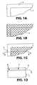
- FIG. 1A- 1 Cshows a corner fragment of a glass carrier in plan view, describing the process steps for creating a polymer base layer on a release layer.
- FIG. 1Dis a cross-sectional view of section DD of FIG. 1C, and shows the base polymer layer in relation to the release layer.
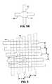
- FIG. 2is a plan view of multi-layer interconnection circuits arrayed on a glass carrier.
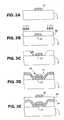
- FIGS. 3 A- 3 Eshows the process steps for creating the first few layers of an interconnection circuit.
- FIG. 4is a cross-sectional view of a multi-layer interconnection circuit of the current invention.
- FIG. 5Ais a cross-sectional view of a stacked contact.
- FIG. 5Bis a plan view of a stacked contact, excluding I/O pad metal.
- FIG. 6is a plan view of metal traces with trace pitch, p.
- FIG. 7is a schematic view of a circuit node connecting between I/O pads on separate IC chips.
- FIG. 8Ais a plan view of a circuit assembly of the current invention.
- FIG. 8Bis a cross-sectional view of section XX of FIG. 8A, and represents a circuit module in process.
- FIGS. 9 A- 9 Cshows details of the preferred flip chip assembly method for an IC chip.
- FIG. 10Ais a plan view of a fragment of an interconnection circuit after additional processing to create the module access port.
- FIG. 10Bshows a test fixture of the current invention, in relation to a circuit assembly.
- FIG. 11is a cross-sectional view of a circuit assembly showing the first module level coatings.
- FIGS. 12 A- 12 Bshows details of the preferred method for connecting a module cable or a test fixture to a circuit module.
- FIG. 13is a schematic view of an RF sputtering machine.
- FIG. 14is a plan view of a module cable of the current invention, connected to a circuit assembly.
- FIG. 15shows a scribe mark on the glass carrier of a module cable.
- FIGS. 16 A- 16 Cshows the process steps for connecting a module cable to a circuit assembly.
- FIG. 17Ashows the method for coating the second topside module-level metal layer.
- FIG. 17Bshows the method for coating the bottom side module-level metal layer.
- FIG. 18is a cross-sectional view of a system module with attached module cable of the current invention.
- FIG. 19is a flow chart summary of the process steps to create a tested circuit assembly.
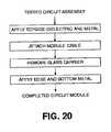
- FIG. 20is a flow chart summary of the additional steps to convert a tested circuit assembly into a completed circuit module.
- FIG. 21is a plan view of a blade server component of the current invention.
- FIG. 22is a cross-sectional view of a circuit module attached to a heat sink.
- FIG. 1Ashows a corner fragment of a glass carrier 1 .
- Photo resisthas been patterned on the carrier, so that a border of resist, 2 , having a width of approximately 20 mm, surrounds the perimeter.
- FIG. 1Bshows that a film of release layer, 3 , has been applied over the entire surface of the glass carrier.
- a suitable material for the release layeris a fluorinated silicone such as F065 manufactured by Gelest, Inc., in Morrisville Pa., USA. This material is a single part gel. It can be applied as a fog or fine spray, or using the spin-on method.
- a suitable thicknessis 2-5 microns after curing, with 2 microns preferred.
- a typical curing cycleis 125° C. for 25 minutes.
- FIG. 1Cshows the result of lifting the resist to pattern the release layer, using a developer or resist stripper to swell the resist and effectuate the lift process; border 4 is clear of release material.
- a base layer 5is then applied.
- Base layer 5is preferably a polymer, and is applied in liquid form with a metering roll or using a spin-on or spraying method.
- a suitable polymeris Cyclotene, a polyimide manufactured by Dow Chemical. No adhesion promoters are used. After curing, a suitable thickness of base layer 5 is 40-80 microns, with 50 microns preferred.
- 1Dis a cross-sectional view of section DD of FIG. 1C, and shows the relation between glass carrier 1 , release layer 3 , and base layer, 5 .
- Surface region 6is characterized by high adhesion between the base layer and the carrier, and surface region 7 is characterized by low adhesion between the base layer and the release layer.
- Base layer 5may later be peeled off of surface region 7 without damage to the base layer or to circuits built thereon.
- An alternative method for providing the base layeris to laminate a preformed sheet of polymeric material onto the glass carrier, while providing for strong adhesion in surface region 6 to anchor the edges of the sheet, and weak adhesion in surface region 7 to facilitate later release.
- FIG. 2shows a glass carrier 1 with a width, W, of 1250 mm, typical of 5 th generation LCD panels.
- a 7 th generation facilityhas been announced that will handle substrates 1800 mm ⁇ 1500 mm.
- any size glass carriercan be used to carry out the present invention, larger sizes result in lower costs for the associated interconnection circuits, including bonding sites fabricated thereon in the form of wells filled with solder, to be further described.
- Materials other than glasscan be used for the carrier, as long as they are rigid and dimensionally stable. Glass is preferred in the current invention because it is well characterized as a substrate material, and it is compatible with mature panel manufacturing methods such as for LCD fabrication.
- Individual multi-layer interconnection circuits 20are arrayed across the glass carrier.
- interconnection circuits 20measure 4 inches by 2 inches, and 220 copies are arrayed on the carrier.
- Multi-layer interconnection circuits 21 and 22have different sizes representing other circuits to be manufactured.
- Border region 23corresponds to surface region 6 of FIG. 1, and is a region of high adhesion between base layer 5 and glass carrier 1 .
- glass carrier 1is diced into interconnection circuits 20 , 21 , and 22 , it can be seen that the resulting circuits include only regions of low adhesion, for easily peeling away the individual glass carriers of interconnection circuits 20 , 21 , and 22 .
- An alternative version of the layout represented in FIG. 2includes streets of high adhesion provided between each of the interconnection circuits, included for improved dimensional stability of the interconnection circuits, and these streets are removed during the dicing operation.
- FIG. 3A-FIG. 3Erepresents the preferred method for forming thin film layers of multilayer interconnection circuit 20 on base layer 5 .
- the metal layers of multi-layer circuit 20are preferably aluminum, deposited by sputtering in a vacuum chamber. A suitable thickness range is 1-2 microns, with 1 micron preferred.
- the metal layersare patterned using conventional photolithographic methods known in the art, and are preferably dry etched using plasma etching processes, also known in the art.
- the patterning of each layertypically includes coating with photo resist, exposing with light through a mask or reticule, developing the resist to form openings where the material is to be removed, and etching of the layer through the openings in the resist. Alternative metals may be used.
- FIG. 1is patterned using plasma etching processes
- a patterned trace of metal 31is shown on base layer 5 .
- this tracehas a width of 5 microns and a thickness of 1 micron.
- a layer of patterned dielectricIn between each layer of patterned metal is a layer of patterned dielectric, to provide isolation in the vertical direction between the metal traces.
- the substrate and metal traceshave been coated with a planarizing layer 32 of a photo-definable polymer as the inter-layer dielectric.
- a suitable photo-definable polymeris photo BCB, benzocyclobutene, a photosensitive form of Cyclotene.
- photo-polymershall be used hereinafter for this material.
- the photo 25 polymeris applied in liquid form to planarize the surface.
- a suitable thickness of photo-polymer layer 32is 2-4 microns after curing, with 2 microns preferred.
- a masked region of photo-polymeris exposed to light where the material is to remain. The effect of light on the photo-polymer is to form cross-linked molecules that become solidified (polymerized) and are not dissolved away in the subsequent development step. Polymer material that is not exposed to light is not cross-linked, remains in liquid form, and is removed by the development step. This is the same mechanism that occurs when patterning a negative photo-resist, and is referred to as negative image development.
- FIG. 3Cshows the result of developing the polymer. The masked illumination of the exposure process causes photons to penetrate the surface of the polymer.
- FIG. 3Cshows the net result of a patterned polymer layer having tapered contact windows with an angle, ⁇ , of approximately 45°, as shown in FIG. 3C.
- FIG. 3Dshows the result of depositing and patterning the next layer of metal, 34 , to form the two-layer contact, 33 between traces 31 and 34 . Because the contact window is tapered rather than vertical, good metal coverage is achieved at the contact walls.
- FIG. 3Eshows the addition of the next photo-polymer layer 35 , and patterning of the next metal layer as metal trace 36 .
- the foregoing descriptionteaches the formation of multi-layer interconnection circuits, with alternating patterned metal and patterned polymer layers, by repeating the foregoing steps.
- FIG. 4is a cross-sectional view of multi-layer interconnection circuit 20 of the present invention, introduced in FIG. 2.
- Base polymer layer 5is shown.
- Conductive trace 41 of first layer metalis shown, with width, w, of 5 microns or less, spacing, s, of 5 microns or less, and thickness, t, of approximately one micron in the preferred embodiment. It may be desirable to arrange conductors on alternate layers to be generally orthogonal as in the figure, as is common practice for layout efficiency.
- a planarizing layer of photo-polymer, 42has been applied over the first layer metal pattern using a roller to meter the thickness, or using spin-on or spray-on methods, with a preferred thickness of two microns after curing.
- a trace of second layer metal, 43forms a two-level contact with a trace 44 of first layer metal.
- the next photo-polymer layer 45again has a preferred thickness of 2 microns, and covers second layer metal 43 with a thickness of 1 micron.
- Photo-polymer layer 45provides a planar surface for deposition and patterning of a third layer metal such as trace 46 .
- Trace 47is fourth layer metal and connects using a two-level contact to a trace 48 of third layer metal as shown. Additional layers are built up in the same manner, as required, and in principle any number of metal layers can be provided.
- trace 49is on the eighth metal layer.
- FIG. 5Ashows an expanded cross-sectional view of a stacked contact 50 at an input/output (I/O) pad.
- Metal traces on alternate layersare preferably orthogonal as shown.
- a trace 51 of first layer metalis shown with a suitable trace width of 8-12 microns in this contact structure, with 10 microns preferred.
- Planarizing layers of photo-polymer such as 52 and 53are used between each metal layer, as described in reference to FIG. 3 and FIG. 4.
- Trace 54 of second layer metalcontacts trace 51 as shown.
- a contact stack of all metal layersis built up layer by layer, with stubs provided for connecting metal traces at any level. Stubs are short metal traces that are provided to establish points of access at each metal layer. Most of them will never connect to anything else.
- Trace stubs 54 , 55 , 56 , and 57are on metal layers 2 , 4 , 6 , and 8 , respectively. Similarly, at 90 degrees rotation from these stubs, the odd numbered metal layers also have similar stubs (not shown).
- I/O pad metal 58connects with the contact stack as shown. It may be convenient to build a stacked contact like 50 at all of the I/O pads. The width of I/O pad metal is approximately 90 microns in the preferred embodiment, providing ample space for such a stacked contact.
- FIG. 5Bshows a plan view of the stacked contact of FIG. 5A, excluding pad layer metal 58 to reveal the locations of the stubs.
- the location of stubs on even-numbered metal layersis shown 59 , and odd-numbered metal layers 60 .
- the common area 61 of the stacked contactis also shown.
- Stacked contact 50is necessarily larger in horizontal area than two-level contact 33 , because of the long sloping contact walls of the stacked contact.
- the trace pitch for parallel runs of metalis a critical parameter for densely packed interconnection circuits. Parallel runs of metal generally require contacts to traces on other layers for effective trace routing of a multi-layer interconnection circuit. To achieve minimum trace pitch for such parallel runs, it is desirable to use contacts of minimum size. This can be accomplished if contacts that are formed at locations other than at the I/O pads are limited to two-level contacts. This is shown in FIG. 6. Horizontal traces such as 64 are on an even-numbered metal layer. Vertical traces such as 65 are on an adjacent odd-numbered metal layer.
- Contact windows 66 and 67are for two-level contacts; they are closely spaced but staggered, and have a minimum contact area.
- the trace pitch pis consistent at 10 microns or less in both directions, and not increased for traces with contacts. This enables dense wiring patterns with predictable space requirements for trace routing programs.
- FIG. 7is a schematic plan view of a circuit node 70 that connects between an I/O pad 50 a on IC chip 71 , and I/O pad 50 b on IC chip 72 .
- a stacked contact 50 ais shown at I/O pad 56 a , as described in reference to FIG. 5.
- Trace 73is on a metal layer below the surface layer, for example on metal layer 7 in a circuit with 8 metal layers. Trace 73 contacts using two-level contact 33 a to trace 74 which is on metal layer 8 in this example.
- a set of parallel metal traces on layer 8is shown, each trace having a width, w, of 5 microns or less in the preferred embodiment.
- Circuit node 70continues from trace 74 to contact 33 b , contacting to trace 75 on metal layer 7 in the example, and terminates at I/O pad 56 b using stacked contact 50 b.
- FIG. 8Ashows circuit assembly 80 with multiple IC chips such as 81 , and other surface-mounted components such as 82 on multi-layer interconnection circuit 20 .
- Components 81 and 82are preferably attached by the flip chip assembly method. Alternatively, surface-mount components may be attached using known solder re-flow techniques.
- Module access port 83provides an array of module access pads (I/O pads) for connection to external signals and power, as well as for connection to internal nodes of the interconnection circuit for testing purposes, as will be further described.
- IC chip 84is a special-purpose test chip in the preferred embodiment, and is preferably the first IC chip to be assembled. For testing different circuit types, such as digital, analog, and radio frequency (RF), it may be desirable to assemble more than one special-purpose test chip. Alternatively, all forms of testing may be accomplished using external testers, accessed through module access port 83 .
- RFradio frequency
- FIG. 8Brepresents a cross-sectional view of section XX of FIG. 8A.
- Circuit assembly 80is supported on release layer 3 on top of glass carrier 1 . It includes interconnection circuit 20 plus attached components.
- IC chip 81is attached using flip chip connections such as 85 , which will be further described with reference to FIG. 9.
- FIGS. 9 A- 9 Cshows a sequence of steps for creating a flip chip bond of the current invention.
- FIG. 9Ashows that an IC chip 71 has been prepared for assembly by forming gold stud bumps such as 91 at I/O bonding pads such as 92 .
- Stud bumps such as 91can be created using a Kulicke and Soffa 8098 bonder, using the application of heat, pressure, and ultrasonic energy.
- the process for forming the ball portion of the stud bumpis the same as for a ball bonder. If an 18-micron diameter gold wire is used, the bonder can be configured to make stud bumps such as 91 with a ball diameter of 50 microns and an overall height of 50 microns.
- FIG. 9Bshows that multi-layer interconnection circuit 20 has been prepared for IC chip assembly by creating wells filled with solder such as 94 at each I/O bonding pad such as 56 a .
- Bonding pad 56 ahas a preferred width of 80-100 microns, with a width of 90 microns in the preferred embodiment. It has been coated with a metallization 95 , to prevent diffusion of solder materials into multi-layer circuit 20 , to provide an oxidation barrier, and also to provide a solder-wetting surface.
- An acceptable sequence of layers for metallization 95is an adhesion layer of aluminum, a solder diffusion layer of nickel, and an oxide prevention layer plus solder wettable layer of copper. This sequence is known in the art as under bump metallization, LBM.
- the bottom of well 94is depressed at the center, 96 , corresponding to the shape of a stacked contact provided at the I/O pad, as described in reference to FIG. 5.
- a planarizing layer 97 of polymer material such as non-photo-definable BCBis formed over the pads, at a thickness of approximately 15 microns when cured.
- Layer 97is etched using known dry etching techniques to create openings at the wells. The openings have vertical walls, as shown in the figure.
- Polymer layer 97is cured to form the solder paste mask and is typically not removed, i.e., it remains a part of the finished circuit assembly.
- Solder paste 98 in well 94is laterally confined by the opening in polymer layer 97 .
- Paste 98is applied using the wiping action of a squeegee over the mask surface. In the preferred embodiment, using a large glass panel as the carrier, several million wells are typically created with one pass of the squeegee.
- 9Cshows a completed flip chip bond 85 of the current invention, with stud bump 91 inserted into well 94 . Since the height variation of the stud bumps is held to ⁇ 2.5 microns, and since the beard is a ridge of small cross-section, and since gold is a soft and malleable material, a small amount of pressure applied to an IC chip will result in the tips of the beards making uniform contact with the bottoms of the wells. The solder paste has been melted and cooled to form a permanent bond. Solder 99 forms a strong mechanical bond with the beard and the underside of the stud bump, as well as a low resistance contact. The width of the well is approximately 34 microns in the preferred embodiment.
- solder materialexamples include Sn/Pb/Sb in percentages 5/95/0, 63/37/0, or 95/0/5 respectively.
- the amount of paste in a wellis approximately 1.5 ⁇ 10 ⁇ 7 gm in the preferred embodiment, at a material cost of approximately US$0.10 (10 cents) per gram.
- the labor and equipment costs of forming wells filled with solderare low for large glass carriers because several million wells are created in parallel. Included in the processing are a photolithographic step to form the solder paste mask, and wiping of a squeegee over the mask to deposit solder paste in the wells.
- the cost per stud bump using the Kulicke and Soffa 8098 bonderis approximately 0.03 cents, based on 200,000 bumps on an 8-inch wafer.
- each flip chip connection in the current inventionis less than 0.05 cents or US$0.0005. This compares with current costs per connection of at least one cent for wire bonding and other flip chip bonding methods.
- Such a low cost for the current inventionmeans that additional test points can be added to the module access port to make testing easier and more effective, perhaps decreasing the overall system cost due to testing economies.
- FIG. 10Arepresents an example of a module access port 83 with individual module access pads such as 101 arrayed as shown.
- the module access padsprovide a means for electrical connection from interconnection circuit 20 or from circuit assembly 80 to other electronic assemblies or devices, and include provision for data signals, control signals, and power.
- a circuit assembly such as 80will typically require several different working voltages for operation.
- power at the highest working voltagewill be delivered through module access port 83 , and local converters and regulators implemented on one or more IC chips will provide other working voltages that are required.
- the converters and regulatorsmay be programmable in order to adjust the working voltages for testing purposes.
- An external testercan be used to validate the integrity of the interconnection circuits prior to assembling IC chips and other components.
- module access pads 101can have a pitch of less than 100 microns, just like flip chip bonding sites 85 . If an interconnection circuit has 4000 nodes, corresponding to a complex system board, then the corresponding area occupied within the module access port to provide 4000 connections is only 0.4 cm 2 at a bonding pitch of 100 microns. Some open circuit testing may also be performed on critical nets (distributed nodes). This is similar in concept to a “bed-of-nails” test that is typically performed on conventional printed circuit boards. In some cases, repair of defective interconnection circuits may be appropriate, preferably using focused ion beams, FIB.
- FIBfocused ion beams
- circuit assembly 80is so dense, both in the fine line traces, and in the fine pitch assembly, that conventional connectors and cables are not well suited for interconnecting modules of this type; they would occupy a large fraction of the total module space. Consequently, part of the current invention is to provide an effective means for connecting circuit assemblies to testers, and circuit modules to other circuit modules or to other electronic systems employing different manufacturing methods. The same methods that are used to fabricate circuit assembly 80 can also be used to fabricate a test fixture and a module cable.
- a test fixture 102is shown connecting to module access port 83 of circuit assembly 80 .
- a redistribution of the module access padsis provided on glass substrate 103 , so as to connect conveniently via cable 104 to an external tester.
- a single layer of aluminumis patterned on glass substrate 103 , with a one-to-one connection between module access pads in the module access port, and corresponding pads in the redistributed array. This can be accomplished if redistributed array 103 is a scaled mirror image of the module access pad array.
- a multi-level interconnection circuitis required. As previously described in reference to FIG.
- stud bumpsare bonded on test fixture 102 . They are provided with a pad pitch of 100 microns at the small end containing the module access port, to mate with wells filled with solder at each of the module access pads. Connection to pads in the redistributed array of test fixture 102 may be accomplished with a conventional flexible circuit, for example. Such a flex circuit may have copper conductors, and may include gold plated bumps that connect by contact with the pads of the redistributed array. The pads of redistributed array 103 may be enlarged, and coated with gold for a low-resistance contact.
- test fixture 102A primary purpose of test fixture 102 is to provide connection means for verifying the integrity of the multi-layer interconnection circuits before any components are assembled. Secondary purposes may include testing of the circuit assembly as each component is attached, if test chips are not provided on the circuit assembly. If test chips are provided, then test fixture 102 may be used to connect these chips to an external tester for verification, prior to assembly of the other components. Connections to the module access port can be unmade by heating the solder and withdrawing the stud bumps. Heat can be applied using a hotplate under the glass carrier, typically bringing it to a temperature below the solder melting point, as well as applying heated inert gas to the top side of glass substrate 103 . After inspection, touch up of the wells may be required. Then another connection to the module access port can be made for a different purpose.
- FIG. 11shows a cross-sectional view of circuit assembly 110 , which is the same as circuit assembly 80 of FIG. 8 except that module level coatings have now been applied.
- fillets 111are shown. They provide support for dielectric coating 112 which is a passivating layer of Parylene in the preferred embodiment.
- the material of fillet 111is silicone rubber or other inert material. It is applied by extruding a bead of the material, then following with a narrow spatula to shape the bead into a triangular cross-section. The fillet material is then cured, and dielectric film 112 and metal film 113 applied.
- Metal film 113is the first topside module-level metal film. It provides a metal coating in the region of the module access port, except for small openings at the module access pads. This area will not be covered by second module-level topside metal, because when that coating is deposited a module cable will be connected at the module access port.
- Metal film 113is preferably aluminum with a thickness of one micron. Other metals and thicknesses can be used. One micron of aluminum provides good hermetic protection, as well as good electromagnetic shielding, at reasonable cost.
- FIG. 12A-FIG. 12Bshow the similarity between flip chip connections 85 for connecting IC chips, already described in reference to FIG. 9, and module access port connections such as 122 , shown in FIG. 12B.
- FIG. 12Ashows multi-layer interconnection circuit 20 on release layer 3 on glass carrier 1 .
- An I/O bonding pad 101is shown, which in this case is a module access pad of module access port 83 .
- Bonding pad 101connects to a circuit node of interconnection circuit 20 using a stacked contact as previously described.
- Metallization 95is shown over the bonding pad, as previously described.
- the pitch between wells filled with solder such as 94is P, which is 100 microns or less in the preferred embodiment.
- Module-level packaging layers 112 and 113are also shown.
- Layer 112is a passivating layer of Parylene
- layer 113is a hermetic and shielding layer of metal as previously described.
- Well 94has been filled with solder paste as previously described, and the paste has been melted into solder form, 121 .
- FIG. 12Bshows an enlarged portion of a module cable inverted over the wells. Gold stud bumps 123 are bonded to metal pads 124 which sit on interconnection circuit 125 on top of release layer 126 , on top of glass carrier 127 (inverted in the figure). Referring to the shape and size of multi-layer circuit 22 in FIG.
- 125 , 126 , and 127may actually be the same as 22 , 3 , and 1 , respectively.
- the path 128 for water to migrate into interconnection circuit 20is shown.
- the surfaces surrounding the wellsare coated with a dielectric, 112 , and a metal layer, 113 , to provide a barrier to water at the module access pads, in the area surrounding but not including the wells.
- the solder in the wellsalso provides an effective water barrier, leaving just a narrow entry point for water, and a long path 128 through the polymer shown as layer 129 in FIG. 12B.
- Polymer layer 129also provides a barrier to water, especially at the preferred thickness of 15 microns.
- the module access padsare semi-hermetic. Since the area of the module access port is small compared with the total surface area of the module, the total exposure to water is limited to a semi-hermetic portion of small extent.
- test fixturesuch as 102 is temporarily attached to the module access port, with the other end connected to a tester.
- the multi-layer interconnection circuitis tested for opens and shorts, and rejected if defective.
- the first chip to be assembledis preferably test chip 84 .
- This chipis also tested by an external tester with capabilities suitable for testing both the functional and parametric specifications of the test chip. If defective, the test chip is replaced. It is heated by application of hot inert gas, the solder in the wells is melted, and the stud bumps lifted out of the wells. The wells are inspected, and touched up if necessary.
- Touch upmay include adding more solder paste, and removing any solder on the surface between the wells. The same procedure is used for rework of any defective IC chips. Once installed and tested, the test chip is capable of testing the remaining components at circuit speed, after each one is attached. Alternatively, each new component may be tested using an external tester, connected using test fixture 102 . The testing of each added component is performed in the system environment of components that have already been assembled. If a component is defective, it is replaced before assembling the next component. If desired, testing can be performed at an elevated temperature applied to the entire circuit assembly, using a heater under the glass carrier.
- test assemblyAfter the circuit assembly has been completely assembled and tested, the test assembly is removed so as not to obstruct the coating of an additional top surface metal layer, as further described in reference to FIG. 17A.
- the overall sequence for creating a tested circuit assemblyis presented in the form of a flow graph in FIG. 19.
- FIG. 13shows a conventional RF sputtering chamber 130 , used for vacuum deposition of metal layers.
- Vacuum chamber 131has an inlet port for a sputtering gas such as argon, and an exit port connected to a vacuum pump as shown.
- Chamber 131includes a top electrode 132 that is connected to an RF source (not shown), and a counter electrode 133 .
- the part to be coated 134normally sits directly on counter-electrode 133 .
- a plasma 135 of ionized gasis formed between the top electrode and the counter-electrode as shown.
- FIG. 14shows a module cable 140 of the present invention, in plan view. It is connected to a circuit module such as 142 , before the glass carrier of 142 is removed to apply the bottom side metal.
- FIG. 15shows module cable 140 with an array of module access pads at each end of the bottom surface (made visible in the figure for descriptive purposes).
- a scribe line 151has been scored in the glass surface with a scribing tool, marking the place where the glass carrier will later be cracked into two separate pieces.
- scribe line 151may be a shallow cut with a diamond saw, positively defining the location of the break to be made, while leaving enough glass thickness to provide adequate strength for handling.
- FIG. 16A through FIG. 16Cshow the sequence for connecting one end of module cable 140 to a circuit assembly such as 142 .
- module cable 140is comprised of a glass carrier 1 a with a release layer 3 a (as previously described) and a single or multi-layer interconnection circuit 161 with stud bumps such as 122 attached at each bonding pad of an array of module access pads.
- a similar array 162is shown at the other end of module cable 140 .
- Interconnection circuit 161includes a single or multi-layer interconnection circuit that connects pads between the two arrays in a one-to-one relationship.
- a cover 163protects the unused end of module cable 140 , including the second array of gold stud bumps 162 , until the module is connected to another circuit module, or to another electronic system.
- Module cable 140can be envisaged in a more complex form, including three or more arrays of module access pads, with each array connecting to a circuit module, or to an electronic system other than a circuit module. One or more of the arrays of module access pads may be redistributed with a larger pad pitch for greater ease of connection to a particular piece of electronic equipment, as was described for test assembly 102 .
- FIG. 16Ashows module cable 140 positioned above circuit assembly 142 .
- FIGS. 12 A- 12 Bshow that a bending force has been applied, to crack the glass carrier into two pieces at scribe line 151 . Crack 164 is shown.
- FIG. 16Cone portion of glass carrier 1 a has been removed by peeling the glass piece away from interconnection circuit 161 , leaving behind interconnection circuit 161 attached to circuit assembly 142 at each of the module access pads.
- a module cable that is connected at one endis labeled 165 .
- FIGS. 17 A- 17 Bshow counter-electrode 133 previously described in reference to FIG. 13.
- FIGS. 17 A- 17 Bshow counter-electrode 133 previously described in reference to FIG. 13.
- FIGS. 17 A- 17 Bshow counter-electrode of RF sputtering chamber 130 .
- the part to be coated in a sputtering chamberrequires deposition on the top surface only, and is placed directly on the counter electrode.
- a pedestal 171is provided on the counter electrode to lift the edges of circuit assembly 172 above the counter electrode, providing a gap between them of a few millimeters.
- the effect of this arrangementis that a top layer metal film 173 will also coat around the edge of the circuit assembly with a thickness that tapers to zero, 174 , underneath circuit assembly 172 .
- the preferred metal film 173is aluminum, with a thickness of one micron, that adds to the first module-level metal film 113 , also with a thickness of one micron.
- a cutout 175is provided in pedestal 171 to store module cable 165 , in a manner that leaves the edges of circuit module 172 exposed for coating.
- circuit module 172becomes circuit module 176 .
- the coatingextends around the edges, 178 .
- the net resultis a continuous metal film covering the top side, the bottom side, and the edges, to form a complete envelope around the circuit assembly.
- An alternative method for creating a metal layer with a coating that extends around the edge like 178is to use a vacuum evaporator. In this case the circuit assembly is held on a carousel, and the carousel executes a planetary motion as is known in the art to effect coating of a substrate from many different angles.
- FIG. 18shows a completed system module 180 whose interconnection circuit and attached components have been thoroughly tested as an integrated system.
- System module 180includes a continuous metal envelope except for small openings at the module access pads, and a module cable that has been attached with fine pitch connections.
- the metal envelopeprovides a hermetic seal. It also provides an effective electrical screen for reducing electromagnetic interference, EMI, and particularly electromagnetic radiation, EMR, produced by the circuit module.
- the metal envelopealso reduces electromagnetic susceptibility, EMS, by reducing the effect of external electronic noise on the circuits within the module.
- FIG. 19shows a summary in the form of a flow chart of the aforementioned process for constructing a circuit assembly of the present invention.
- FIG. 20shows a summary in the form of a flow chart of the aforementioned process for constructing a system module from a circuit assembly.
- FIG. 21shows an alternative embodiment of a circuit assembly, such as for a blade server component, 210 , of the current invention.
- a single large interconnection circuit 211contrasts with the array of smaller interconnection circuits 20 shown in FIG. 2.
- Processing groups of IC chips 212are arrayed as shown. Each processing group may include processor chips, memory chips, and bus-interface chips, for example.
- the dense interconnection circuits and assembly methods of the current inventionprovide for a large computational capability on circuit assembly 210 .
- a module access port 213is shown, for connecting to other systems, including test systems.
- a group of special-purpose programmable test chipsis provided, 214 , and also a maintenance group of IC chips 215 , for maintenance of the blade server.
- any failure occurring in a processing groupmay be automatically detected by a background process running on maintenance group 215 , which will reconfigure blade server component 210 to bypass the defective group for any further operations.
- the same methods as previously described for incremental assembly and testmay be applied to blade server component 210 .
- circuit assembly 210has been converted into circuit module 220 by application of module-level coatings, as previously described.
- FIG. 22shows a fragment of circuit module 220 coupled with a heat sink 221 .
- Circuit module 220includes multi-layer interconnection circuit 211 (manufactured as previously described for interconnection circuit 20 ) with IC chips such as 222 attached by flip chip bonds 85 , as previously described.
- module-level coatings including dielectric layer 223 and metal envelope 224are fabricated using the same methods as previously described for circuit module 176 .
- Circuit module 220is attached to heat sink 221 at the faces of chips such as 222 , using pads of conductive epoxy 225 that are screened onto completed module 220 at each attached IC chip.
- Heat sink 221preferably contains a re-circulating coolant fluid, to extract heat effectively using a heat sink of small volume.
- Circuit module 220 and heat sink 221combine to form a blade server component that can be inserted into a large computer facility, with appropriate provisions for electrical and plumbing connections.
- the thermal path from active transistor junctions on IC chips such as 222 to heat sink 221has low thermal impedance. It includes only one layer of non-conducting material, which is preferably a thin layer of Parylene 223 in the current invention. This means that IC chips of blade server module 220 can operate at high power levels, without exceeding their maximum junction temperature specifications.
Landscapes
- Engineering & Computer Science (AREA)
- Microelectronics & Electronic Packaging (AREA)
- Power Engineering (AREA)
- Computer Hardware Design (AREA)
- Physics & Mathematics (AREA)
- General Physics & Mathematics (AREA)
- Condensed Matter Physics & Semiconductors (AREA)
- Manufacturing & Machinery (AREA)
- Geometry (AREA)
- Production Of Multi-Layered Print Wiring Board (AREA)
- Tests Of Electronic Circuits (AREA)
- Combinations Of Printed Boards (AREA)
- Wire Bonding (AREA)
Abstract
Description
- This application claims priority to Provisional Application Serial No. 60/318,271 filed Sep. 7, 2001.[0001]
- 1. Field of the Invention[0002]
- This invention relates generally to an electronic system module and method of fabrication, and more particularly to an electronic system module fabricated on a carrier from which it can be released.[0003]
- 2. Description of the Related Art[0004]
- The number of input/output (I/O) connections required by integrated circuit (IC) chips is increasing, to several hundred for recent microprocessor chips. As verification of complex designs becomes an increasing portion of the total design activity, it is desirable to increase the I/O count further, to provide access to more internal nodes for testing. Flip chip assembly methods have helped to provide more I/O connections because they provide an area array of connections across the entire face of an IC chip, rather than just at the perimeter as with wire bonding. However, it continues to be desirable to reduce the pad pitch, the distance between bonding pad centers, in order to achieve more I/O connections per unit area of IC chip.[0005]
- A recent advance in flip chip assembly capability has been the introduction of stud bumping machines that can provide gold stud bumps on IC chips with pad pitches of less than 100 microns. However, to take advantage of this capability, the system board that receives the bumped devices must have fine traces in order to route all of the signals with space efficiency, and to support bonding pitches less than 100 microns. The most recent packaging technology to be commercially introduced is called land grid array, LGA. It builds up the wiring layers by plating a base layer of copper that has been patterned with photo resist. The external terminal pitch claimed for this packaging method is “less than 0.5 mm”. None of the available printed circuit board technologies can support direct mounting of bumped devices at a pitch of 100 microns or less. The current invention is capable of pad pitches of less than 100 microns, including a viable method for reworking defective IC chips at this bonding density.[0006]
- For many years the minimum trace width available from printed circuit board vendors has been around 100 microns. Recently, advanced multi-layer circuit processes have achieved trace widths of 17 microns. The current invention is capable of achieving trace widths of 5 microns or less, together with a trace pitch of 10 microns or less.[0007]
- One way to achieve fine line interconnection circuits is to employ a semiconductor fabrication facility and to build the interconnection circuit on a silicon wafer; hence the term, wafer level packaging, WLP. The precision of the associated photolithographic methods, the clean room environment with low particulate count, and the advanced substrate handling equipment of such a facility can all contribute to high-density interconnection circuits. However, the application of IC chip manufacturing facilities to this problem is more than what is required. An intermediate alternative is to apply the manufacturing resources of a glass panel fabrication facility, where the minimum feature sizes are 10 to 20 times larger than for IC chips (but still adequate for the most advanced assembly processes), and the manufacturing cost per unit area of devices produced is less than 5% of the cost per unit area of IC chips. In addition, the glass panel fabrication facility can produce system boards of any size up to approximately a meter square, whereas the largest wafers produced have a diameter of 300 mm. In order to avoid the rigidity and weight of the glass substrate, and to provide better thermal access to the heat producing components for cooling them, it is desirable to discard the glass carrier after most of the processing is done.[0008]
- Typically, WLP has used redistribution circuits to map from the fine pitch available with flip chip bonding to the coarser pitch of a printed circuit board. The current invention eliminates the redistribution circuits because the printed circuits produced (termed interconnection circuits) include fine features that easily accommodate the fine pitch of the flip chip bonding.[0009]
- It has been common practice to produce printed circuit boards at one facility, and perform system assembly and test at another facility. However, there are major advantages to integrating the circuit board manufacturing process with the assembly and test process to create a single, unified, fabrication, assembly, and test process. One advantage is in reducing the time to develop and debug a new design. Flexibility in the proposed process allows adaptation to component and assembly yield problems as they arise (as each additional component is assembled), providing more detailed testing sequences as necessary. For example, during prototype testing, components may be assembled onto the circuit substrate one at a time, providing a test environment of a partial system, and making the minimum change of a single IC chip between one test and the next. The test software can be adapted to address detailed issues as they arise. Once confidence has been achieved at this level, components may be assembled and tested in functional groups as the product moves into production. A tighter integration of personnel is also achieved because all of the variables are controlled in one place. This flexibility, wherein the assembly process is tailored to yield issues in real time, is not available with conventional testing methods. Usually, an entire system is assembled before any system testing is performed. The current invention employs incremental system level testing, as each component is attached to the circuit assembly. The testing of each component is performed fewer times, because the incremental assembly and test process essentially guarantees system integrity at each step. This contrasts with conventional methods requiring component test, subassembly test, and system test, with numerous iterations if problems develop.[0010]
- More accurate and complete testing of components is provided when they are tested in their system environment, rather than individually. The system environment is created with the actual system, or a subset thereof, rather than a simulated environment created by test vectors programmed into a general-purpose tester. This can lead to lower test cost and faster test development, by eliminating the need to generate and debug detailed system response patterns. If the system level requirements are satisfactorily met, then the minutiae of component level characteristics become irrelevant. Alternatively, only the functions relevant to proper system function are tested; this is a much more manageable set of requirements than the total set of functions that all the assembled components are capable of performing.[0011]
- The signal voltage swing is reducing with each new generation of IC chip technology. This makes it more difficult to test remotely through a cable, and still achieve the necessary noise margins. Providing test chips on the motherboard will provide shorter trace lengths for testing, which will be more robust with respect to both timing issues and noise margin.[0012]
- Each component may be verified at an elevated system temperature before attaching the next component. This can be accomplished by heating the glass carrier underneath the circuit assembly. By providing a predetermined test temperature to the entire circuit assembly, a speed grade can be associated with the module, as has been done in the past at the component level. Greater emphasis can be placed on environmental stress testing at the system level. Also accelerated life testing can be performed early in the life cycle of a product, and lessons learned about particular components can be incorporated into the system level test. The only tests performed on each component correspond to system level requirements; by not testing component requirements that are irrelevant to the particular system, higher system yields may be achievable.[0013]
- The physical structure of the system module of the current invention can lead to other conveniences. An example relates to accelerated life testing of a module. Because the current invention allows a sophisticated system (circuit assembly) to be implemented in a module of small size, and because the system module packaging includes a metal envelope surrounding the module that provides good heat distribution, temperature control can be achieved by placing the module on a hot plate rather than in a bulky and inaccessible environmental chamber.[0014]
- Hermetic packaging techniques and electromagnetic shielding techniques can be applied at the module level to improve both performance and manufacturing cost. Performance is improved because a single metal envelope encloses almost the entire module, avoiding the interference from individual components and the wiring between them. Cost is reduced because hermeticity and shielding are provided with a simple process applied once to the entire system, rather than being addressed individually at each of the components.[0015]
- Such a unified process has only recently become feasible. It depends on using common semiconductor manufacturing equipment to support fabrication of the interconnection circuits, bonding sites, test connection fixtures, module cables, and the module layers that create hermeticity and electromagnetic shielding. It also depends on the fact that sophisticated and programmable IC chips can now implement the testing function across all of the components in a system, including digital, analog, and RF functions, if multiple IC chips are employed for testing. Adding these functions to the system using the current invention is not as expensive as in the past, because the packaging and assembly cost is minimal. Preferably, a tester is included with every module produced, but the cost of the tester is small compared with the system level assembly and performance benefits, and the reduction in system development time.[0016]
- R. K. Traeger, “Hermeticity of Polymeric Lid Sealants”, Proc. 25[0017]thElectronics Components Conf., 1976, p.361, has documented the water permeabilities of silicones, epoxies, fluorocarbons, glasses and metals. Traeger's data shows that, in terms of providing a barrier to water, a layer of metal that is 1 micron thick is approximately equivalent to a layer of glass that is 1 mm thick, and also equivalent to a layer of epoxy that is 100 cm thick.
- Generally flip chip bonding techniques require an epoxy under-layer between flip chip mounted IC chips and the circuit board. The purpose of the under-layer is to provide mechanical strength to withstand repeated thermal cycling without developing cracks in the area of the flip chip bonds. The thermal stress arises because of the difference in thermal coefficients of expansion (TCEs) between the IC chip material and the board material. Gelatinized solvents have typically been used to dissolve the epoxy; they leave a residue that must be cleaned off. The process of cleaning off the residue has typically resulted in damage to the fine pitch bonding sites, to the point where they cannot be reliably re-bonded. The under-layer is unnecessary with the current invention because the flexibility of the final interconnection circuit substantially eliminates thermally induced stress in the region of the flip chip bonds. Without the thermally induced stress, no cracking will occur. Thermal stresses are still present during assembly (because the interconnection circuit is rigid at this point), but are avoided during operation in the field (when the interconnection circuit is flexible). The number and extent of thermal cycles during assembly are more predictable and controllable than the thermal cycles arising from operation in the field. Stress testing in the laboratory can be used to quantify the acceptable temperature limits, and assure crack-free circuit assemblies. Avoiding the under-layer makes a robust rework process possible. This general concept is referred to in the art as compliant packaging technology. A related issue is the recent requirement for low stress in IC chips that use ultra-low-k dielectric materials. IC chips attached to flexible substrates will experience low stress and will be accommodating of the ultra-low-k dielectrics.[0018]
- A glass substrate for 5[0019]thgeneration fabrication of LCD circuits is typically 1100 by 1250 mm in area, and 1.1 mm thick, which can be used in carrying out the present invention. However, the glass carrier of the current invention can be of any size. The unit manufacturing costs of interconnection circuits and related circuit assemblies of the current invention are lower if larger glass panels are used. The glass or other rigid carrier provides mechanical support for all of the fabrication, component assembly, test, and rework process steps, and also has excellent dimensional stability. This dimensional stability transfers to the multi-layer circuits that are built up as a series of films on top of the glass. This transferred dimensional stability is a primary reason that fine line features such as trace widths less than 5 microns are possible with the current invention. It is also important however, that the final version of the interconnection circuit be flexible, because the flexibility allows the use of epoxy under layers to be avoided, leading to more robust rework processes for removing and replacing defective chips. The flexibility also allows system boards to be folded in compact devices such as cellular phones.
- A release agent is applied to a glass panel substrate, except for a clear region near the edges. The clear region is characterized by high adhesion between the glass and the polymer base layer to be subsequently formed on the glass. The high adhesion region provides an anchor that firmly attaches the polymer to the glass around the perimeter of the panel. The release layer creates low adhesion between glass and polymer, so that after a circuit assembly has been built on top, it can be readily peeled off.[0020]
- Alternate layers of metal interconnect and dielectric such as a photo-definable polymer are built up on the base layer. Two-level contacts are formed between adjacent metal layers, and stacked contacts are provided between groups of adjacent layers. Preferably each input/output (I/O) pad of an assembled IC chip is a node of the multi-layer interconnection circuit. At the center of each I/O pad a stacked contact is created, with stubs at every metal layer, for convenient routing of traces. The base polymer layer, the dielectric layers and the metal layers are flexible, and when the multi-layer interconnection circuit is subsequently removed from the glass panel, it too is flexible. Attached IC chips are usually not flexible, but if a folding line on the interconnection circuit is kept clear of IC chips, then the circuit assembly can be folded at the folding line.[0021]
- While the multi-layer interconnection circuit is still attached to the glass carrier, it is convenient to form wells filled with solder on the array of interconnection circuits, in large substrate form. Each well is designed to accept a stud bump of an attached component. Gold stud bumps are formed at I/O pads of all IC chips to be assembled. To create the wells a thick layer of polymer is applied on top of the interconnection circuit. Openings in this layer are formed at I/O pad bonding sites. The openings in the cured polymer layer form a mask, and solder paste is wiped over the mask to fill the openings, thus forming a well at each of the I/O bonding sites.[0022]
- The glass carrier is diced with a diamond saw to separate individual circuit assemblies from one another, and provide a more convenient form for component assembly, test, and rework. The interconnection circuit itself must be tested, before any assembly is done. This test is performed using a test fixture that connects through a module access port to an external tester. The module access port may include I/O pads (module access pads) for every node of the multilayer interconnection circuit. The assembly and rework steps require that IC chips and other surface mounted components are precisely located in order that the bonding tool can accurately align bonding sites on the components with corresponding bonding sites on the interconnection circuit. Accordingly, the circuit assembly remains attached to the glass carrier, and its dimensional accuracy is maintained until these steps are completed.[0023]
- A module cable with high-density interconnections is attached to each circuit assembly. The circuit assemblies are then separated from their individual glass carriers by peeling the base substrate away from the carrier. Since the adhesion force is low in these regions, they can be separated without damage.[0024]
- Additional metal coatings are applied to create a circuit module that is hermetically sealed and electro-magnetically shielded. To effectively cool the dense circuit module, it may be bonded to a heat sink, and the heat sink may be cooled with a circulating fluid.[0025]
- FIG. 1A-[0026]1C shows a corner fragment of a glass carrier in plan view, describing the process steps for creating a polymer base layer on a release layer.
- FIG. 1D is a cross-sectional view of section DD of FIG. 1C, and shows the base polymer layer in relation to the release layer.[0027]
- FIG. 2 is a plan view of multi-layer interconnection circuits arrayed on a glass carrier.[0028]
- FIGS.[0029]3A-3E shows the process steps for creating the first few layers of an interconnection circuit.
- FIG. 4 is a cross-sectional view of a multi-layer interconnection circuit of the current invention.[0030]
- FIG. 5A is a cross-sectional view of a stacked contact.[0031]
- FIG. 5B is a plan view of a stacked contact, excluding I/O pad metal.[0032]
- FIG. 6 is a plan view of metal traces with trace pitch, p.[0033]
- FIG. 7 is a schematic view of a circuit node connecting between I/O pads on separate IC chips.[0034]
- FIG. 8A is a plan view of a circuit assembly of the current invention.[0035]
- FIG. 8B is a cross-sectional view of section XX of FIG. 8A, and represents a circuit module in process.[0036]
- FIGS.[0037]9A-9C shows details of the preferred flip chip assembly method for an IC chip.
- FIG. 10A is a plan view of a fragment of an interconnection circuit after additional processing to create the module access port.[0038]
- FIG. 10B shows a test fixture of the current invention, in relation to a circuit assembly.[0039]
- FIG. 11 is a cross-sectional view of a circuit assembly showing the first module level coatings.[0040]
- FIGS.[0041]12A-12B shows details of the preferred method for connecting a module cable or a test fixture to a circuit module.
- FIG. 13 is a schematic view of an RF sputtering machine.[0042]
- FIG. 14 is a plan view of a module cable of the current invention, connected to a circuit assembly.[0043]
- FIG. 15 shows a scribe mark on the glass carrier of a module cable.[0044]
- FIGS.[0045]16A-16C shows the process steps for connecting a module cable to a circuit assembly.
- FIG. 17A shows the method for coating the second topside module-level metal layer.[0046]
- FIG. 17B shows the method for coating the bottom side module-level metal layer.[0047]
- FIG. 18 is a cross-sectional view of a system module with attached module cable of the current invention.[0048]
- FIG. 19 is a flow chart summary of the process steps to create a tested circuit assembly.[0049]
- FIG. 20 is a flow chart summary of the additional steps to convert a tested circuit assembly into a completed circuit module.[0050]
- FIG. 21 is a plan view of a blade server component of the current invention.[0051]
- FIG. 22 is a cross-sectional view of a circuit module attached to a heat sink.[0052]
- It should be understood that for diagrammatic purposes the figures are not drawn to scale.[0053]
- FIG. 1A shows a corner fragment of a[0054]
glass carrier 1. Photo resist has been patterned on the carrier, so that a border of resist,2, having a width of approximately 20 mm, surrounds the perimeter. FIG. 1B shows that a film of release layer,3, has been applied over the entire surface of the glass carrier. A suitable material for the release layer is a fluorinated silicone such as F065 manufactured by Gelest, Inc., in Morrisville Pa., USA. This material is a single part gel. It can be applied as a fog or fine spray, or using the spin-on method. A suitable thickness is 2-5 microns after curing, with 2 microns preferred. A typical curing cycle is 125° C. for 25 minutes. This release material has a silane component that bonds well to glass surfaces, yet presents a fluid-like interface to polymeric materials like the base layer to be subsequently applied. FIG. 1C shows the result of lifting the resist to pattern the release layer, using a developer or resist stripper to swell the resist and effectuate the lift process; border4 is clear of release material. Abase layer 5 is then applied.Base layer 5 is preferably a polymer, and is applied in liquid form with a metering roll or using a spin-on or spraying method. A suitable polymer is Cyclotene, a polyimide manufactured by Dow Chemical. No adhesion promoters are used. After curing, a suitable thickness ofbase layer 5 is 40-80 microns, with 50 microns preferred. FIG. 1D is a cross-sectional view of section DD of FIG. 1C, and shows the relation betweenglass carrier 1,release layer 3, and base layer,5. Surface region6 is characterized by high adhesion between the base layer and the carrier, andsurface region 7 is characterized by low adhesion between the base layer and the release layer.Base layer 5 may later be peeled off ofsurface region 7 without damage to the base layer or to circuits built thereon. An alternative method for providing the base layer is to laminate a preformed sheet of polymeric material onto the glass carrier, while providing for strong adhesion in surface region6 to anchor the edges of the sheet, and weak adhesion insurface region 7 to facilitate later release. - FIG. 2 shows a[0055]
glass carrier 1 with a width, W, of 1250 mm, typical of 5thgeneration LCD panels. A 7thgeneration facility has been announced that will handle substrates 1800 mm×1500 mm. Although any size glass carrier can be used to carry out the present invention, larger sizes result in lower costs for the associated interconnection circuits, including bonding sites fabricated thereon in the form of wells filled with solder, to be further described. Materials other than glass can be used for the carrier, as long as they are rigid and dimensionally stable. Glass is preferred in the current invention because it is well characterized as a substrate material, and it is compatible with mature panel manufacturing methods such as for LCD fabrication. Individualmulti-layer interconnection circuits 20 are arrayed across the glass carrier. In this example,interconnection circuits 20 measure 4 inches by 2 inches, and 220 copies are arrayed on the carrier.Multi-layer interconnection circuits Border region 23 corresponds to surface region6 of FIG. 1, and is a region of high adhesion betweenbase layer 5 andglass carrier 1. Whenglass carrier 1 is diced intointerconnection circuits interconnection circuits - FIG. 3A-FIG. 3E represents the preferred method for forming thin film layers of[0056]
multilayer interconnection circuit 20 onbase layer 5. The metal layers ofmulti-layer circuit 20 are preferably aluminum, deposited by sputtering in a vacuum chamber. A suitable thickness range is 1-2 microns, with 1 micron preferred. The metal layers are patterned using conventional photolithographic methods known in the art, and are preferably dry etched using plasma etching processes, also known in the art. The patterning of each layer typically includes coating with photo resist, exposing with light through a mask or reticule, developing the resist to form openings where the material is to be removed, and etching of the layer through the openings in the resist. Alternative metals may be used. In FIG. 3A a patterned trace ofmetal 31 is shown onbase layer 5. For example, this trace has a width of 5 microns and a thickness of 1 micron. In between each layer of patterned metal is a layer of patterned dielectric, to provide isolation in the vertical direction between the metal traces. In FIG. 3B, the substrate and metal traces have been coated with aplanarizing layer 32 of a photo-definable polymer as the inter-layer dielectric. A suitable photo-definable polymer is photo BCB, benzocyclobutene, a photosensitive form of Cyclotene. The term “photo-polymer” shall be used hereinafter for this material. The photo25 polymer is applied in liquid form to planarize the surface. A suitable thickness of photo-polymer layer 32 is 2-4 microns after curing, with 2 microns preferred. In FIG. 3B a masked region of photo-polymer is exposed to light where the material is to remain. The effect of light on the photo-polymer is to form cross-linked molecules that become solidified (polymerized) and are not dissolved away in the subsequent development step. Polymer material that is not exposed to light is not cross-linked, remains in liquid form, and is removed by the development step. This is the same mechanism that occurs when patterning a negative photo-resist, and is referred to as negative image development. FIG. 3C shows the result of developing the polymer. The masked illumination of the exposure process causes photons to penetrate the surface of the polymer. The photons spread laterally as they penetrate to lower depths, causing cross-linking as they spread. The net result is a patterned polymer layer having tapered contact windows with an angle, θ, of approximately 45°, as shown in FIG. 3C. FIG. 3D shows the result of depositing and patterning the next layer of metal,34, to form the two-layer contact,33 betweentraces polymer layer 35, and patterning of the next metal layer asmetal trace 36. The foregoing description teaches the formation of multi-layer interconnection circuits, with alternating patterned metal and patterned polymer layers, by repeating the foregoing steps. - FIG. 4 is a cross-sectional view of[0057]
multi-layer interconnection circuit 20 of the present invention, introduced in FIG. 2.Base polymer layer 5 is shown.Conductive trace 41 of first layer metal is shown, with width, w, of 5 microns or less, spacing, s, of 5 microns or less, and thickness, t, of approximately one micron in the preferred embodiment. It may be desirable to arrange conductors on alternate layers to be generally orthogonal as in the figure, as is common practice for layout efficiency. A planarizing layer of photo-polymer,42, has been applied over the first layer metal pattern using a roller to meter the thickness, or using spin-on or spray-on methods, with a preferred thickness of two microns after curing. A trace of second layer metal,43, forms a two-level contact with atrace 44 of first layer metal. The next photo-polymer layer 45 again has a preferred thickness of 2 microns, and coverssecond layer metal 43 with a thickness of 1 micron. Photo-polymer layer 45 provides a planar surface for deposition and patterning of a third layer metal such astrace 46.Trace 47 is fourth layer metal and connects using a two-level contact to atrace 48 of third layer metal as shown. Additional layers are built up in the same manner, as required, and in principle any number of metal layers can be provided. In the figure, trace49 is on the eighth metal layer. - FIG. 5A shows an expanded cross-sectional view of a[0058]
stacked contact 50 at an input/output (I/O) pad. Metal traces on alternate layers are preferably orthogonal as shown. Atrace 51 of first layer metal is shown with a suitable trace width of 8-12 microns in this contact structure, with 10 microns preferred. Planarizing layers of photo-polymer such as52 and53 are used between each metal layer, as described in reference to FIG. 3 and FIG. 4.Trace 54 of second layer metal contacts trace51 as shown. A contact stack of all metal layers is built up layer by layer, with stubs provided for connecting metal traces at any level. Stubs are short metal traces that are provided to establish points of access at each metal layer. Most of them will never connect to anything else. However, some of them will be extended into circuit traces of the interconnection circuit. Trace stubs54,55,56, and57, are onmetal layers 2,4,6, and8, respectively. Similarly, at 90 degrees rotation from these stubs, the odd numbered metal layers also have similar stubs (not shown). Finally I/O pad metal 58 connects with the contact stack as shown. It may be convenient to build a stacked contact like50 at all of the I/O pads. The width of I/O pad metal is approximately 90 microns in the preferred embodiment, providing ample space for such a stacked contact. It is convenient for the circuit board layout designer to know that every node in the circuit is available at all metal layers (using the stubs), and at a known location. FIG. 5B shows a plan view of the stacked contact of FIG. 5A, excludingpad layer metal 58 to reveal the locations of the stubs. The location of stubs on even-numbered metal layers is shown59, and odd-numbered metal layers60. Thecommon area 61 of the stacked contact is also shown. - [0059]
Stacked contact 50 is necessarily larger in horizontal area than two-level contact 33, because of the long sloping contact walls of the stacked contact. The trace pitch for parallel runs of metal is a critical parameter for densely packed interconnection circuits. Parallel runs of metal generally require contacts to traces on other layers for effective trace routing of a multi-layer interconnection circuit. To achieve minimum trace pitch for such parallel runs, it is desirable to use contacts of minimum size. This can be accomplished if contacts that are formed at locations other than at the I/O pads are limited to two-level contacts. This is shown in FIG. 6. Horizontal traces such as64 are on an even-numbered metal layer. Vertical traces such as65 are on an adjacent odd-numbered metal layer. Contactwindows - FIG. 7 is a schematic plan view of a[0060]
circuit node 70 that connects between an I/O pad 50aonIC chip 71, and I/O pad50bonIC chip 72. Astacked contact 50ais shown at I/O pad 56a, as described in reference to FIG. 5.Trace 73 is on a metal layer below the surface layer, for example onmetal layer 7 in a circuit with8 metal layers.Trace 73 contacts using two-level contact 33ato trace74 which is on metal layer8 in this example. A set of parallel metal traces on layer8 is shown, each trace having a width, w, of 5 microns or less in the preferred embodiment. The separation, s, between traces is also 5 microns or less in the preferred embodiment. The I/O pad pitch, P, is 100 microns or less in the preferred embodiment.Circuit node 70 continues fromtrace 74 to contact33b, contacting to trace75 onmetal layer 7 in the example, and terminates at I/O pad 56busing stacked contact50b. - Having explained the details of building a high density interconnect structure in the form of a flexible multi-layer interconnection circuit, we shall now focus on assembly and testing of IC chips on the interconnection circuit, to form a circuit assembly.[0061]
- FIG. 8A shows[0062]
circuit assembly 80 with multiple IC chips such as81, and other surface-mounted components such as82 onmulti-layer interconnection circuit 20.Components Module access port 83 provides an array of module access pads (I/O pads) for connection to external signals and power, as well as for connection to internal nodes of the interconnection circuit for testing purposes, as will be further described.IC chip 84 is a special-purpose test chip in the preferred embodiment, and is preferably the first IC chip to be assembled. For testing different circuit types, such as digital, analog, and radio frequency (RF), it may be desirable to assemble more than one special-purpose test chip. Alternatively, all forms of testing may be accomplished using external testers, accessed throughmodule access port 83. - FIG. 8B represents a cross-sectional view of section XX of FIG.[0063]
8A. Circuit assembly 80 is supported onrelease layer 3 on top ofglass carrier 1. It includesinterconnection circuit 20 plus attached components.IC chip 81 is attached using flip chip connections such as85, which will be further described with reference to FIG. 9. - FIGS.[0064]9A-9C shows a sequence of steps for creating a flip chip bond of the current invention. FIG. 9A shows that an
IC chip 71 has been prepared for assembly by forming gold stud bumps such as91 at I/O bonding pads such as92. Stud bumps such as91 can be created using a Kulicke and Soffa 8098 bonder, using the application of heat, pressure, and ultrasonic energy. The process for forming the ball portion of the stud bump is the same as for a ball bonder. If an 18-micron diameter gold wire is used, the bonder can be configured to make stud bumps such as91 with a ball diameter of 50 microns and an overall height of 50 microns. The “beard”93 is created by accurately shearing the gold wire, and the tips of the beards can be coplanar within ±2.5 microns. FIG. 9B shows thatmulti-layer interconnection circuit 20 has been prepared for IC chip assembly by creating wells filled with solder such as94 at each I/O bonding pad such as56a.Bonding pad 56ahas a preferred width of 80-100 microns, with a width of 90 microns in the preferred embodiment. It has been coated with ametallization 95, to prevent diffusion of solder materials intomulti-layer circuit 20, to provide an oxidation barrier, and also to provide a solder-wetting surface. An acceptable sequence of layers formetallization 95 is an adhesion layer of aluminum, a solder diffusion layer of nickel, and an oxide prevention layer plus solder wettable layer of copper. This sequence is known in the art as under bump metallization, LBM. The bottom of well94 is depressed at the center,96, corresponding to the shape of a stacked contact provided at the I/O pad, as described in reference to FIG. 5. Aplanarizing layer 97 of polymer material such as non-photo-definable BCB is formed over the pads, at a thickness of approximately 15 microns when cured.Layer 97 is etched using known dry etching techniques to create openings at the wells. The openings have vertical walls, as shown in the figure. This is not generally possible using photo-polymers such as photo BCB, and this is why dry etching is used, with an anisotropic etching characteristic as is known in the art.Polymer layer 97 is cured to form the solder paste mask and is typically not removed, i.e., it remains a part of the finished circuit assembly.Solder paste 98 inwell 94 is laterally confined by the opening inpolymer layer 97.Paste 98 is applied using the wiping action of a squeegee over the mask surface. In the preferred embodiment, using a large glass panel as the carrier, several million wells are typically created with one pass of the squeegee. FIG. 9C shows a completedflip chip bond 85 of the current invention, withstud bump 91 inserted intowell 94. Since the height variation of the stud bumps is held to ±2.5 microns, and since the beard is a ridge of small cross-section, and since gold is a soft and malleable material, a small amount of pressure applied to an IC chip will result in the tips of the beards making uniform contact with the bottoms of the wells. The solder paste has been melted and cooled to form a permanent bond.Solder 99 forms a strong mechanical bond with the beard and the underside of the stud bump, as well as a low resistance contact. The width of the well is approximately 34 microns in the preferred embodiment. The foregoing dimensions, together with the precise photolithographic patterning achievable with glass processing fabs, and the dimensional stability of the interconnection substrate (base polymer layer) with underlying glass, make a pad pitch P of less than 100 microns achievable. Examples of solder material that are suitable for the current invention include Sn/Pb/Sb inpercentages 5/95/0, 63/37/0, or 95/0/5 respectively. - The amount of paste in a well is approximately 1.5×10[0065]−7gm in the preferred embodiment, at a material cost of approximately US$0.10 (10 cents) per gram. The labor and equipment costs of forming wells filled with solder are low for large glass carriers because several million wells are created in parallel. Included in the processing are a photolithographic step to form the solder paste mask, and wiping of a squeegee over the mask to deposit solder paste in the wells. The cost per stud bump using the Kulicke and Soffa 8098 bonder is approximately 0.03 cents, based on 200,000 bumps on an 8-inch wafer. Consequently, the cost of each flip chip connection in the current invention, including the stud bump and the corresponding well, is less than 0.05 cents or US$0.0005. This compares with current costs per connection of at least one cent for wire bonding and other flip chip bonding methods. Such a low cost for the current invention means that additional test points can be added to the module access port to make testing easier and more effective, perhaps decreasing the overall system cost due to testing economies.
- FIG. 10A represents an example of a[0066]
module access port 83 with individual module access pads such as101 arrayed as shown. The module access pads provide a means for electrical connection frominterconnection circuit 20 or fromcircuit assembly 80 to other electronic assemblies or devices, and include provision for data signals, control signals, and power. A circuit assembly such as80 will typically require several different working voltages for operation. Preferably, power at the highest working voltage will be delivered throughmodule access port 83, and local converters and regulators implemented on one or more IC chips will provide other working voltages that are required. The converters and regulators may be programmable in order to adjust the working voltages for testing purposes. An external tester can be used to validate the integrity of the interconnection circuits prior to assembling IC chips and other components. It may be advantageous to provide a module access pad for every node on the interconnection circuit, to provide 100% test coverage for short circuits. If a module cable of the current invention is used, as further described with reference to FIG. 14 through FIG. 18,module access pads 101 can have a pitch of less than 100 microns, just like flipchip bonding sites 85. If an interconnection circuit has 4000 nodes, corresponding to a complex system board, then the corresponding area occupied within the module access port to provide 4000 connections is only 0.4 cm2at a bonding pitch of 100 microns. Some open circuit testing may also be performed on critical nets (distributed nodes). This is similar in concept to a “bed-of-nails” test that is typically performed on conventional printed circuit boards. In some cases, repair of defective interconnection circuits may be appropriate, preferably using focused ion beams, FIB. - The layout of[0067]
circuit assembly 80 is so dense, both in the fine line traces, and in the fine pitch assembly, that conventional connectors and cables are not well suited for interconnecting modules of this type; they would occupy a large fraction of the total module space. Consequently, part of the current invention is to provide an effective means for connecting circuit assemblies to testers, and circuit modules to other circuit modules or to other electronic systems employing different manufacturing methods. The same methods that are used to fabricatecircuit assembly 80 can also be used to fabricate a test fixture and a module cable. - In FIG. 10B, a[0068]
test fixture 102 is shown connecting tomodule access port 83 ofcircuit assembly 80. A redistribution of the module access pads is provided onglass substrate 103, so as to connect conveniently viacable 104 to an external tester. For small arrays of module access pads, a single layer of aluminum is patterned onglass substrate 103, with a one-to-one connection between module access pads in the module access port, and corresponding pads in the redistributed array. This can be accomplished if redistributedarray 103 is a scaled mirror image of the module access pad array. For larger arrays, a multi-level interconnection circuit is required. As previously described in reference to FIG. 9 for creating stud bumps on IC chips, so stud bumps are bonded ontest fixture 102. They are provided with a pad pitch of 100 microns at the small end containing the module access port, to mate with wells filled with solder at each of the module access pads. Connection to pads in the redistributed array oftest fixture 102 may be accomplished with a conventional flexible circuit, for example. Such a flex circuit may have copper conductors, and may include gold plated bumps that connect by contact with the pads of the redistributed array. The pads of redistributedarray 103 may be enlarged, and coated with gold for a low-resistance contact. A primary purpose oftest fixture 102 is to provide connection means for verifying the integrity of the multi-layer interconnection circuits before any components are assembled. Secondary purposes may include testing of the circuit assembly as each component is attached, if test chips are not provided on the circuit assembly. If test chips are provided, then testfixture 102 may be used to connect these chips to an external tester for verification, prior to assembly of the other components. Connections to the module access port can be unmade by heating the solder and withdrawing the stud bumps. Heat can be applied using a hotplate under the glass carrier, typically bringing it to a temperature below the solder melting point, as well as applying heated inert gas to the top side ofglass substrate 103. After inspection, touch up of the wells may be required. Then another connection to the module access port can be made for a different purpose. - Before permanently assembling a module cable to the circuit assembly, it is desirable to coat the top surface with a dielectric layer and a metal layer. The dielectric layer prevents shorting of components when the metal layer is subsequently applied. The metal layer provides a shield at the top surface, except for small holes at the module access pads, as will be further described in reference to FIG. 12. FIG. 11 shows a cross-sectional view of[0069]
circuit assembly 110, which is the same ascircuit assembly 80 of FIG. 8 except that module level coatings have now been applied. At the edges of components, where vertical faces meetinterconnection circuit 20,fillets 111 are shown. They provide support fordielectric coating 112 which is a passivating layer of Parylene in the preferred embodiment. The material offillet 111 is silicone rubber or other inert material. It is applied by extruding a bead of the material, then following with a narrow spatula to shape the bead into a triangular cross-section. The fillet material is then cured, anddielectric film 112 andmetal film 113 applied.Metal film 113 is the first topside module-level metal film. It provides a metal coating in the region of the module access port, except for small openings at the module access pads. This area will not be covered by second module-level topside metal, because when that coating is deposited a module cable will be connected at the module access port.Metal film 113 is preferably aluminum with a thickness of one micron. Other metals and thicknesses can be used. One micron of aluminum provides good hermetic protection, as well as good electromagnetic shielding, at reasonable cost. - FIG. 12A-FIG. 12B show the similarity between[0070]
flip chip connections 85 for connecting IC chips, already described in reference to FIG. 9, and module access port connections such as122, shown in FIG. 12B. FIG. 12A showsmulti-layer interconnection circuit 20 onrelease layer 3 onglass carrier 1. An I/O bonding pad 101 is shown, which in this case is a module access pad ofmodule access port 83.Bonding pad 101 connects to a circuit node ofinterconnection circuit 20 using a stacked contact as previously described.Metallization 95 is shown over the bonding pad, as previously described. The pitch between wells filled with solder such as94 is P, which is 100 microns or less in the preferred embodiment. Module-level packaging layers112 and113 are also shown.Layer 112 is a passivating layer of Parylene, andlayer 113 is a hermetic and shielding layer of metal as previously described. Well94 has been filled with solder paste as previously described, and the paste has been melted into solder form,121. FIG. 12B shows an enlarged portion of a module cable inverted over the wells. Gold stud bumps123 are bonded tometal pads 124 which sit oninterconnection circuit 125 on top ofrelease layer 126, on top of glass carrier127 (inverted in the figure). Referring to the shape and size ofmulti-layer circuit 22 in FIG. 2, and understanding that a common manufacturing process may be used to fabricate circuit assemblies and module cables, it can be seen that125,126, and127, may actually be the same as22,3, and1, respectively. Thepath 128 for water to migrate intointerconnection circuit 20 is shown. The surfaces surrounding the wells are coated with a dielectric,112, and a metal layer,113, to provide a barrier to water at the module access pads, in the area surrounding but not including the wells. The solder in the wells also provides an effective water barrier, leaving just a narrow entry point for water, and along path 128 through the polymer shown aslayer 129 in FIG. 12B.Polymer layer 129 also provides a barrier to water, especially at the preferred thickness of 15 microns. Thus the module access pads are semi-hermetic. Since the area of the module access port is small compared with the total surface area of the module, the total exposure to water is limited to a semi-hermetic portion of small extent. - Referring back to FIG. 8A, the assembly and test sequence of the electrical components such as[0071]
IC chip 81 will now be discussed. Before assembling any components, a test fixture such as102 is temporarily attached to the module access port, with the other end connected to a tester. The multi-layer interconnection circuit is tested for opens and shorts, and rejected if defective. The first chip to be assembled is preferablytest chip 84. This chip is also tested by an external tester with capabilities suitable for testing both the functional and parametric specifications of the test chip. If defective, the test chip is replaced. It is heated by application of hot inert gas, the solder in the wells is melted, and the stud bumps lifted out of the wells. The wells are inspected, and touched up if necessary. Touch up may include adding more solder paste, and removing any solder on the surface between the wells. The same procedure is used for rework of any defective IC chips. Once installed and tested, the test chip is capable of testing the remaining components at circuit speed, after each one is attached. Alternatively, each new component may be tested using an external tester, connected usingtest fixture 102. The testing of each added component is performed in the system environment of components that have already been assembled. If a component is defective, it is replaced before assembling the next component. If desired, testing can be performed at an elevated temperature applied to the entire circuit assembly, using a heater under the glass carrier. After the circuit assembly has been completely assembled and tested, the test assembly is removed so as not to obstruct the coating of an additional top surface metal layer, as further described in reference to FIG. 17A. The overall sequence for creating a tested circuit assembly is presented in the form of a flow graph in FIG. 19. - FIG. 13 shows a conventional[0072]
RF sputtering chamber 130, used for vacuum deposition of metal layers.Vacuum chamber 131 has an inlet port for a sputtering gas such as argon, and an exit port connected to a vacuum pump as shown.Chamber 131 includes atop electrode 132 that is connected to an RF source (not shown), and acounter electrode 133. The part to be coated134 normally sits directly oncounter-electrode 133. During sputtering, aplasma 135 of ionized gas is formed between the top electrode and the counter-electrode as shown. These details are provided as background for a modification to this apparatus, further described in reference to FIGS. 17A and 17B, wherein a pedestal is used to raise the part to be coated above the counter-electrode. - FIG. 14 shows a[0073]
module cable 140 of the present invention, in plan view. It is connected to a circuit module such as142, before the glass carrier of142 is removed to apply the bottom side metal. - FIG. 15[0074]
shows module cable 140 with an array of module access pads at each end of the bottom surface (made visible in the figure for descriptive purposes). On the top surface, ascribe line 151 has been scored in the glass surface with a scribing tool, marking the place where the glass carrier will later be cracked into two separate pieces. Alternatively,scribe line 151 may be a shallow cut with a diamond saw, positively defining the location of the break to be made, while leaving enough glass thickness to provide adequate strength for handling. FIG. 16A through FIG. 16C show the sequence for connecting one end ofmodule cable 140 to a circuit assembly such as142. To maintain the necessary dimensional stability, it is critical that a glass carrier be present on both sides of the connection interface while the bond sites on both sides are aligned and the bonds are permanently created. In FIG. 16A,module cable 140 is comprised of aglass carrier 1awith a release layer3a(as previously described) and a single ormulti-layer interconnection circuit 161 with stud bumps such as122 attached at each bonding pad of an array of module access pads. Asimilar array 162 is shown at the other end ofmodule cable 140.Interconnection circuit 161 includes a single or multi-layer interconnection circuit that connects pads between the two arrays in a one-to-one relationship. Acover 163 protects the unused end ofmodule cable 140, including the second array of gold stud bumps162, until the module is connected to another circuit module, or to another electronic system.Module cable 140 can be envisaged in a more complex form, including three or more arrays of module access pads, with each array connecting to a circuit module, or to an electronic system other than a circuit module. One or more of the arrays of module access pads may be redistributed with a larger pad pitch for greater ease of connection to a particular piece of electronic equipment, as was described fortest assembly 102. FIG. 16A showsmodule cable 140 positioned abovecircuit assembly 142. When correct alignment has been achieved, heat is applied to form permanent bonds between stud bumps onmodule cable 140, and corresponding wells filled with solder oncircuit assembly 142. This connection is as described in FIGS.12A-12B. FIG. 16B shows that a bending force has been applied, to crack the glass carrier into two pieces atscribe line 151. Crack164 is shown. In FIG. 16C, one portion ofglass carrier 1ahas been removed by peeling the glass piece away frominterconnection circuit 161, leaving behindinterconnection circuit 161 attached tocircuit assembly 142 at each of the module access pads. A module cable that is connected at one end is labeled165. - It is desired to create a continuous metal envelope around the circuit assembly including the interconnection circuit and the attached components, with only a small opening at each of the module access pads. It is critical that the top and bottom metal layers form an overlapping seam of continuous metal at the edge of the circuit assembly. A preferred method for achieving this is shown in FIGS.[0075]17A-17B. FIG. 17A shows counter-electrode133 previously described in reference to FIG. 13. For convenience, only the counter-electrode of
RF sputtering chamber 130 will be shown in FIGS.17A-17B. Normally, the part to be coated in a sputtering chamber requires deposition on the top surface only, and is placed directly on the counter electrode. In the current invention, apedestal 171 is provided on the counter electrode to lift the edges ofcircuit assembly 172 above the counter electrode, providing a gap between them of a few millimeters. The effect of this arrangement is that a toplayer metal film 173 will also coat around the edge of the circuit assembly with a thickness that tapers to zero,174, underneathcircuit assembly 172. Thepreferred metal film 173 is aluminum, with a thickness of one micron, that adds to the first module-level metal film 113, also with a thickness of one micron. Aftertop layer metal 173 has been deposited, the circuit assembly is flipped onpedestal 171 as shown in FIG. 17B. Acutout 175 is provided inpedestal 171 to storemodule cable 165, in a manner that leaves the edges ofcircuit module 172 exposed for coating. After deposition ofbottom side metal 177,circuit module 172 becomescircuit module 176. Again, the coating extends around the edges,178. The net result is a continuous metal film covering the top side, the bottom side, and the edges, to form a complete envelope around the circuit assembly. An alternative method for creating a metal layer with a coating that extends around the edge like178, is to use a vacuum evaporator. In this case the circuit assembly is held on a carousel, and the carousel executes a planetary motion as is known in the art to effect coating of a substrate from many different angles. - FIG. 18 shows a completed[0076]
system module 180 whose interconnection circuit and attached components have been thoroughly tested as an integrated system.System module 180 includes a continuous metal envelope except for small openings at the module access pads, and a module cable that has been attached with fine pitch connections. The metal envelope provides a hermetic seal. It also provides an effective electrical screen for reducing electromagnetic interference, EMI, and particularly electromagnetic radiation, EMR, produced by the circuit module. The metal envelope also reduces electromagnetic susceptibility, EMS, by reducing the effect of external electronic noise on the circuits within the module. - FIG. 19 shows a summary in the form of a flow chart of the aforementioned process for constructing a circuit assembly of the present invention.[0077]
- FIG. 20 shows a summary in the form of a flow chart of the aforementioned process for constructing a system module from a circuit assembly.[0078]
- FIG. 21 shows an alternative embodiment of a circuit assembly, such as for a blade server component,[0079]210, of the current invention. A single
large interconnection circuit 211 contrasts with the array ofsmaller interconnection circuits 20 shown in FIG. 2. Processing groups ofIC chips 212 are arrayed as shown. Each processing group may include processor chips, memory chips, and bus-interface chips, for example. The dense interconnection circuits and assembly methods of the current invention provide for a large computational capability oncircuit assembly 210. Amodule access port 213 is shown, for connecting to other systems, including test systems. A group of special-purpose programmable test chips is provided,214, and also a maintenance group ofIC chips 215, for maintenance of the blade server. For example, any failure occurring in a processing group may be automatically detected by a background process running onmaintenance group 215, which will reconfigureblade server component 210 to bypass the defective group for any further operations. The same methods as previously described for incremental assembly and test may be applied toblade server component 210. - In FIG. 22,[0080]
circuit assembly 210 has been converted intocircuit module 220 by application of module-level coatings, as previously described. FIG. 22 shows a fragment ofcircuit module 220 coupled with aheat sink 221.Circuit module 220 includes multi-layer interconnection circuit211 (manufactured as previously described for interconnection circuit20) with IC chips such as222 attached byflip chip bonds 85, as previously described. Similarly, module-level coatings includingdielectric layer 223 andmetal envelope 224 are fabricated using the same methods as previously described forcircuit module 176.Circuit module 220 is attached toheat sink 221 at the faces of chips such as222, using pads ofconductive epoxy 225 that are screened onto completedmodule 220 at each attached IC chip.Heat sink 221 preferably contains a re-circulating coolant fluid, to extract heat effectively using a heat sink of small volume.Circuit module 220 andheat sink 221 combine to form a blade server component that can be inserted into a large computer facility, with appropriate provisions for electrical and plumbing connections. The thermal path from active transistor junctions on IC chips such as222 toheat sink 221 has low thermal impedance. It includes only one layer of non-conducting material, which is preferably a thin layer ofParylene 223 in the current invention. This means that IC chips ofblade server module 220 can operate at high power levels, without exceeding their maximum junction temperature specifications.
Claims (55)
Priority Applications (11)
| Application Number | Priority Date | Filing Date | Title |
|---|---|---|---|
| US10/237,640US6927471B2 (en) | 2001-09-07 | 2002-09-06 | Electronic system modules and method of fabrication |
| US10/701,888US6881609B2 (en) | 2001-09-07 | 2003-11-04 | Component connections using bumps and wells |
| US10/702,235US7297572B2 (en) | 2001-09-07 | 2003-11-05 | Fabrication method for electronic system modules |
| US11/066,964US20050140026A1 (en) | 2001-09-07 | 2005-02-25 | Fabrication methods for electronic system modules |
| US11/769,321US7615478B2 (en) | 2001-09-07 | 2007-06-27 | Fabrication method for electronic system modules |
| US11/868,919US20080079140A1 (en) | 2001-09-07 | 2007-10-08 | Electronic system modules and method of fabricaton |
| US11/868,912US7723156B2 (en) | 2001-09-07 | 2007-10-10 | Electronic system modules and method of fabrication |
| US12/414,502US8581407B2 (en) | 2001-09-07 | 2009-03-30 | Electronic system modules and method of fabrication |
| US12/550,327US8633584B2 (en) | 2001-09-07 | 2009-08-28 | Electronic assembly with electronic compontent and interconnection assembly connected via conductive bump and mating well |
| US12/786,314US8252635B2 (en) | 2001-09-07 | 2010-05-24 | Electronic system modules and method of fabrication |
| US14/077,126US9059070B2 (en) | 2001-09-07 | 2013-11-11 | Electronic system modules and method of fabrication |
Applications Claiming Priority (2)
| Application Number | Priority Date | Filing Date | Title |
|---|---|---|---|
| US31827101P | 2001-09-07 | 2001-09-07 | |
| US10/237,640US6927471B2 (en) | 2001-09-07 | 2002-09-06 | Electronic system modules and method of fabrication |
Related Child Applications (3)
| Application Number | Title | Priority Date | Filing Date |
|---|---|---|---|
| US10/701,888Continuation-In-PartUS6881609B2 (en) | 2001-09-07 | 2003-11-04 | Component connections using bumps and wells |
| US10/702,235Continuation-In-PartUS7297572B2 (en) | 2001-09-07 | 2003-11-05 | Fabrication method for electronic system modules |
| US11/066,964DivisionUS20050140026A1 (en) | 2001-09-07 | 2005-02-25 | Fabrication methods for electronic system modules |
Publications (2)
| Publication Number | Publication Date |
|---|---|
| US20030049886A1true US20030049886A1 (en) | 2003-03-13 |
| US6927471B2 US6927471B2 (en) | 2005-08-09 |
Family
ID=26930880
Family Applications (4)
| Application Number | Title | Priority Date | Filing Date |
|---|---|---|---|
| US10/237,640Expired - LifetimeUS6927471B2 (en) | 2001-09-07 | 2002-09-06 | Electronic system modules and method of fabrication |
| US11/066,964AbandonedUS20050140026A1 (en) | 2001-09-07 | 2005-02-25 | Fabrication methods for electronic system modules |
| US12/414,502Expired - LifetimeUS8581407B2 (en) | 2001-09-07 | 2009-03-30 | Electronic system modules and method of fabrication |
| US14/077,126Expired - Fee RelatedUS9059070B2 (en) | 2001-09-07 | 2013-11-11 | Electronic system modules and method of fabrication |
Family Applications After (3)
| Application Number | Title | Priority Date | Filing Date |
|---|---|---|---|
| US11/066,964AbandonedUS20050140026A1 (en) | 2001-09-07 | 2005-02-25 | Fabrication methods for electronic system modules |
| US12/414,502Expired - LifetimeUS8581407B2 (en) | 2001-09-07 | 2009-03-30 | Electronic system modules and method of fabrication |
| US14/077,126Expired - Fee RelatedUS9059070B2 (en) | 2001-09-07 | 2013-11-11 | Electronic system modules and method of fabrication |
Country Status (1)
| Country | Link |
|---|---|
| US (4) | US6927471B2 (en) |
Cited By (78)
| Publication number | Priority date | Publication date | Assignee | Title |
|---|---|---|---|---|
| US20030111736A1 (en)* | 2001-12-14 | 2003-06-19 | Roeters Glen E. | Csp chip stack with flex circuit |
| US20030137048A1 (en)* | 2001-10-26 | 2003-07-24 | Staktek Group, L.P. | Stacking system and method |
| US20030155406A1 (en)* | 2002-02-21 | 2003-08-21 | Ho-Ming Tong | Bump manufacturing method |
| US20040000707A1 (en)* | 2001-10-26 | 2004-01-01 | Staktek Group, L.P. | Modularized die stacking system and method |
| US6732908B2 (en)* | 2002-01-18 | 2004-05-11 | International Business Machines Corporation | High density raised stud microjoining system and methods of fabricating the same |
| US20040195666A1 (en)* | 2001-10-26 | 2004-10-07 | Julian Partridge | Stacked module systems and methods |
| US20040201091A1 (en)* | 2001-10-26 | 2004-10-14 | Staktek Group, L.P. | Stacked module systems and methods |
| US20040229402A1 (en)* | 2001-10-26 | 2004-11-18 | Staktek Group, L.P. | Low profile chip scale stacking system and method |
| US20040235222A1 (en)* | 2001-10-26 | 2004-11-25 | Staktek Group, L.P. | Integrated circuit stacking system and method |
| US20040245615A1 (en)* | 2003-06-03 | 2004-12-09 | Staktek Group, L.P. | Point to point memory expansion system and method |
| US20050009234A1 (en)* | 2001-10-26 | 2005-01-13 | Staktek Group, L.P. | Stacked module systems and methods for CSP packages |
| US20050017368A1 (en)* | 2002-12-20 | 2005-01-27 | Atila Mertol | Multi-level redistribution layer traces for reducing current crowding in flipchip solder bumps |
| US20050018412A1 (en)* | 2001-10-26 | 2005-01-27 | Staktek Group, L.P. | Pitch change and chip scale stacking system |
| US20050041403A1 (en)* | 2001-10-26 | 2005-02-24 | Staktek Group, L.P. | Integrated circuit stacking system and method |
| US20050057911A1 (en)* | 2003-09-15 | 2005-03-17 | Staktek Group, L.P. | Memory expansion and integrated circuit stacking system and method |
| US20050056921A1 (en)* | 2003-09-15 | 2005-03-17 | Staktek Group L.P. | Stacked module systems and methods |
| US20050062144A1 (en)* | 2001-10-26 | 2005-03-24 | Staktek Group, L.P. | Memory expansion and chip scale stacking system and method |
| US20050072597A1 (en)* | 2003-10-02 | 2005-04-07 | Chun-Yu Lee | Bonding pad structure for a display device and fabrication method thereof |
| US20050139980A1 (en)* | 1992-12-11 | 2005-06-30 | Burns Carmen D. | High density integrated circuit module |
| US20050146011A1 (en)* | 2001-10-26 | 2005-07-07 | Staktek Group, L.P. | Pitch change and chip scale stacking system and method |
| US20050146031A1 (en)* | 2001-10-26 | 2005-07-07 | Staktek Group, L.P. | Low profile stacking system and method |
| US20060033187A1 (en)* | 2004-08-12 | 2006-02-16 | Staktek Group, L.P. | Rugged CSP module system and method |
| US20060043558A1 (en)* | 2004-09-01 | 2006-03-02 | Staktek Group L.P. | Stacked integrated circuit cascade signaling system and method |
| US20060050592A1 (en)* | 2004-09-03 | 2006-03-09 | Staktek Group L.P. | Compact module system and method |
| US20060050496A1 (en)* | 2004-09-03 | 2006-03-09 | Staktek Group L.P. | Thin module system and method |
| US20060049500A1 (en)* | 2004-09-03 | 2006-03-09 | Staktek Group L.P. | Thin module system and method |
| US20060049502A1 (en)* | 2004-09-03 | 2006-03-09 | Staktek Group, L.P. | Module thermal management system and method |
| US20060050488A1 (en)* | 2004-09-03 | 2006-03-09 | Staktel Group, L.P. | High capacity thin module system and method |
| US20060049513A1 (en)* | 2004-09-03 | 2006-03-09 | Staktek Group L.P. | Thin module system and method with thermal management |
| US20060050498A1 (en)* | 2004-09-03 | 2006-03-09 | Staktek Group L.P. | Die module system and method |
| US20060055024A1 (en)* | 2004-09-14 | 2006-03-16 | Staktek Group, L.P. | Adapted leaded integrated circuit module |
| US20060072297A1 (en)* | 2004-10-01 | 2006-04-06 | Staktek Group L.P. | Circuit Module Access System and Method |
| US7033861B1 (en) | 2005-05-18 | 2006-04-25 | Staktek Group L.P. | Stacked module systems and method |
| US20060118936A1 (en)* | 2004-12-03 | 2006-06-08 | Staktek Group L.P. | Circuit module component mounting system and method |
| US20060157842A1 (en)* | 2005-01-20 | 2006-07-20 | Staktek Group L.P. | Inverted CSP stacking system and method |
| US20060175693A1 (en)* | 2005-02-04 | 2006-08-10 | Staktek Group, L.P. | Systems, methods, and apparatus for generating ball-out matrix configuration output for a flex circuit |
| US20060198238A1 (en)* | 2004-09-03 | 2006-09-07 | Staktek Group L.P. | Modified core for circuit module system and method |
| US20060203442A1 (en)* | 2004-09-03 | 2006-09-14 | Staktek Group, L.P. | Memory module system and method |
| US20060244114A1 (en)* | 2005-04-28 | 2006-11-02 | Staktek Group L.P. | Systems, methods, and apparatus for connecting a set of contacts on an integrated circuit to a flex circuit via a contact beam |
| US20060250780A1 (en)* | 2005-05-06 | 2006-11-09 | Staktek Group L.P. | System component interposer |
| US20060255446A1 (en)* | 2001-10-26 | 2006-11-16 | Staktek Group, L.P. | Stacked modules and method |
| US20060261449A1 (en)* | 2005-05-18 | 2006-11-23 | Staktek Group L.P. | Memory module system and method |
| USRE39628E1 (en) | 1999-05-05 | 2007-05-15 | Stakick Group, L.P. | Stackable flex circuit IC package and method of making same |
| US20070201208A1 (en)* | 2006-02-27 | 2007-08-30 | Staktek Group L.P. | Active cooling methods and apparatus for modules |
| US7310458B2 (en) | 2001-10-26 | 2007-12-18 | Staktek Group L.P. | Stacked module systems and methods |
| US7417310B2 (en) | 2006-11-02 | 2008-08-26 | Entorian Technologies, Lp | Circuit module having force resistant construction |
| US7443023B2 (en) | 2004-09-03 | 2008-10-28 | Entorian Technologies, Lp | High capacity thin module system |
| US7446410B2 (en) | 2004-09-03 | 2008-11-04 | Entorian Technologies, Lp | Circuit module with thermal casing systems |
| US7511969B2 (en) | 2006-02-02 | 2009-03-31 | Entorian Technologies, Lp | Composite core circuit module system and method |
| US7511968B2 (en) | 2004-09-03 | 2009-03-31 | Entorian Technologies, Lp | Buffered thin module system and method |
| US7522421B2 (en) | 2004-09-03 | 2009-04-21 | Entorian Technologies, Lp | Split core circuit module |
| US20090108427A1 (en)* | 2007-10-30 | 2009-04-30 | International Business Machines Corporation | Techniques for Modular Chip Fabrication |
| US7542297B2 (en) | 2004-09-03 | 2009-06-02 | Entorian Technologies, Lp | Optimized mounting area circuit module system and method |
| US7579687B2 (en) | 2004-09-03 | 2009-08-25 | Entorian Technologies, Lp | Circuit module turbulence enhancement systems and methods |
| US7616452B2 (en) | 2004-09-03 | 2009-11-10 | Entorian Technologies, Lp | Flex circuit constructions for high capacity circuit module systems and methods |
| USRE41039E1 (en) | 2000-01-13 | 2009-12-15 | Entorian Technologies, Lp | Stackable chip package with flex carrier |
| US7656678B2 (en) | 2001-10-26 | 2010-02-02 | Entorian Technologies, Lp | Stacked module systems |
| EP2162237A4 (en)* | 2007-07-02 | 2011-01-12 | 3M Innovative Properties Co | Method of patterning a substrate |
| US20140065321A1 (en)* | 2012-08-31 | 2014-03-06 | Apple Inc. | Pull-back design to mitigate plastic sensor cracks |
| US20140127865A1 (en)* | 2012-01-04 | 2014-05-08 | Mediatek Inc. | Molded interposer package and method for fabricating the same |
| US20140159245A1 (en)* | 2002-08-29 | 2014-06-12 | Renesas Electronics Corporation | Semiconductor device and a method of manufacturing the same |
| US8767351B1 (en)* | 2013-01-31 | 2014-07-01 | Seagate Technology Llc | Ambient temperature ball bond |
| US20160013162A1 (en)* | 2010-05-20 | 2016-01-14 | Taiwan Semiconductor Manufacturing Company, Ltd. | Substrate Interconnections having Different Sizes |
| US20160133590A1 (en)* | 2011-12-15 | 2016-05-12 | Pramod Malatkar | Packaged Semiconductor Die with Bumpless Die-Package Interface for Bumpless Build-Up Layer (BBUL) Packages |
| WO2016209302A1 (en)* | 2015-06-25 | 2016-12-29 | Hanergy Technologies, Inc. | Mobile charge/discharge device |
| CN107369664A (en)* | 2017-09-05 | 2017-11-21 | 中芯长电半导体(江阴)有限公司 | The encapsulating structure and method for packing of semiconductor chip |
| US9953939B2 (en) | 2012-09-18 | 2018-04-24 | Taiwan Semiconductor Manufacturing Company, Ltd. | Conductive contacts having varying widths and method of manufacturing same |
| US9991224B2 (en) | 2012-04-18 | 2018-06-05 | Taiwan Semiconductor Manufacturing Company, Ltd. | Bump-on-trace interconnect having varying widths and methods of forming same |
| US10056345B2 (en) | 2012-04-17 | 2018-08-21 | Taiwan Semiconductor Manufacturing Company, Ltd. | Conical-shaped or tier-shaped pillar connections |
| US10211141B1 (en) | 2017-11-17 | 2019-02-19 | General Electric Company | Semiconductor logic device and system and method of embedded packaging of same |
| US10228720B2 (en) | 2012-06-08 | 2019-03-12 | Apple Inc. | Internal components of a portable computing device |
| US10276523B1 (en) | 2017-11-17 | 2019-04-30 | General Electric Company | Semiconductor logic device and system and method of embedded packaging of same |
| CN110010511A (en)* | 2018-10-10 | 2019-07-12 | 浙江集迈科微电子有限公司 | A kind of test mode of radio frequency chip system in package mould group |
| US10396053B2 (en)* | 2017-11-17 | 2019-08-27 | General Electric Company | Semiconductor logic device and system and method of embedded packaging of same |
| US10566301B2 (en) | 2017-11-17 | 2020-02-18 | General Electric Company | Semiconductor logic device and system and method of embedded packaging of same |
| CN113853058A (en)* | 2021-10-25 | 2021-12-28 | 深圳市宝明科技股份有限公司 | A circuit board and method of making the same |
| EP4440253A3 (en)* | 2012-12-20 | 2025-01-01 | INTEL Corporation | High density organic bridge device and method |
| US12211801B2 (en) | 2018-10-18 | 2025-01-28 | Parabellum Strategic Opportunities Fund Llc | Chip package and method of forming the same |
Families Citing this family (55)
| Publication number | Priority date | Publication date | Assignee | Title |
|---|---|---|---|---|
| US6927471B2 (en)* | 2001-09-07 | 2005-08-09 | Peter C. Salmon | Electronic system modules and method of fabrication |
| US7297572B2 (en)* | 2001-09-07 | 2007-11-20 | Hynix Semiconductor, Inc. | Fabrication method for electronic system modules |
| KR100519795B1 (en)* | 2003-02-07 | 2005-10-10 | 삼성전자주식회사 | Photo mask set for forming multi-layered interconnection lines and semiconductor device fabricated using the same |
| US7505862B2 (en)* | 2003-03-07 | 2009-03-17 | Salmon Technologies, Llc | Apparatus and method for testing electronic systems |
| US7408258B2 (en)* | 2003-08-20 | 2008-08-05 | Salmon Technologies, Llc | Interconnection circuit and electronic module utilizing same |
| US7262075B2 (en)* | 2004-01-08 | 2007-08-28 | Georgia Tech Research Corp. | High-aspect-ratio metal-polymer composite structures for nano interconnects |
| US20050184376A1 (en)* | 2004-02-19 | 2005-08-25 | Salmon Peter C. | System in package |
| US20050255722A1 (en)* | 2004-05-07 | 2005-11-17 | Salmon Peter C | Micro blade assembly |
| US7163830B2 (en)* | 2004-10-12 | 2007-01-16 | Salmon Peter C | Method for temporarily engaging electronic component for test |
| US7427809B2 (en)* | 2004-12-16 | 2008-09-23 | Salmon Technologies, Llc | Repairable three-dimensional semiconductor subsystem |
| TWI240400B (en)* | 2005-01-04 | 2005-09-21 | Nan Ya Printed Circuit Board C | Method for fabricating a packaging substrate |
| US20070007983A1 (en)* | 2005-01-06 | 2007-01-11 | Salmon Peter C | Semiconductor wafer tester |
| US7586747B2 (en)* | 2005-08-01 | 2009-09-08 | Salmon Technologies, Llc. | Scalable subsystem architecture having integrated cooling channels |
| US20070023889A1 (en)* | 2005-08-01 | 2007-02-01 | Salmon Peter C | Copper substrate with feedthroughs and interconnection circuits |
| US20070023904A1 (en)* | 2005-08-01 | 2007-02-01 | Salmon Peter C | Electro-optic interconnection apparatus and method |
| US20070023923A1 (en)* | 2005-08-01 | 2007-02-01 | Salmon Peter C | Flip chip interface including a mixed array of heat bumps and signal bumps |
| US7457132B2 (en)* | 2005-10-20 | 2008-11-25 | Sanmina-Sci Corporation | Via stub termination structures and methods for making same |
| US7576995B2 (en) | 2005-11-04 | 2009-08-18 | Entorian Technologies, Lp | Flex circuit apparatus and method for adding capacitance while conserving circuit board surface area |
| US7608920B2 (en) | 2006-01-11 | 2009-10-27 | Entorian Technologies, Lp | Memory card and method for devising |
| US7304382B2 (en) | 2006-01-11 | 2007-12-04 | Staktek Group L.P. | Managed memory component |
| US7605454B2 (en) | 2006-01-11 | 2009-10-20 | Entorian Technologies, Lp | Memory card and method for devising |
| US7508058B2 (en) | 2006-01-11 | 2009-03-24 | Entorian Technologies, Lp | Stacked integrated circuit module |
| US7508069B2 (en) | 2006-01-11 | 2009-03-24 | Entorian Technologies, Lp | Managed memory component |
| TWI299888B (en)* | 2006-05-03 | 2008-08-11 | Touch Micro System Tech | Method of fabricating micro connectors |
| CN100536259C (en)* | 2006-05-15 | 2009-09-02 | 探微科技股份有限公司 | Method for manufacturing micro connector |
| US7944048B2 (en)* | 2006-08-09 | 2011-05-17 | Monolithic Power Systems, Inc. | Chip scale package for power devices and method for making the same |
| US7666321B2 (en)* | 2006-09-26 | 2010-02-23 | United Microelectronics Corp. | Method for decapsulating package |
| US7468553B2 (en) | 2006-10-20 | 2008-12-23 | Entorian Technologies, Lp | Stackable micropackages and stacked modules |
| US7750466B2 (en)* | 2007-09-07 | 2010-07-06 | Intel Corporation | Microelectronic assembly having second level interconnects including solder joints reinforced with crack arrester elements and method of forming same |
| US8293587B2 (en) | 2007-10-11 | 2012-10-23 | International Business Machines Corporation | Multilayer pillar for reduced stress interconnect and method of making same |
| CN101939825B (en)* | 2008-02-07 | 2013-04-03 | 住友电木株式会社 | Film for semiconductor, method for manufacturing semiconductor device and semiconductor device |
| JP4539773B2 (en)* | 2008-03-07 | 2010-09-08 | 株式会社デンソー | Semiconductor device and manufacturing method thereof |
| US8129267B2 (en) | 2008-03-21 | 2012-03-06 | International Business Machines Corporation | Alpha particle blocking wire structure and method fabricating same |
| US20090243051A1 (en)* | 2008-03-28 | 2009-10-01 | Micron Technology, Inc. | Integrated conductive shield for microelectronic device assemblies and associated methods |
| US8693203B2 (en) | 2011-01-14 | 2014-04-08 | Harris Corporation | Method of making an electronic device having a liquid crystal polymer solder mask laminated to an interconnect layer stack and related devices |
| US9835648B2 (en)* | 2011-06-30 | 2017-12-05 | Intel Corporation | Liquid metal interconnects |
| US8643150B1 (en) | 2012-02-15 | 2014-02-04 | Maxim Integrated Products, Inc. | Wafer-level package device having solder bump assemblies that include an inner pillar structure |
| US9583425B2 (en) | 2012-02-15 | 2017-02-28 | Maxim Integrated Products, Inc. | Solder fatigue arrest for wafer level package |
| KR102142521B1 (en)* | 2013-12-26 | 2020-08-07 | 삼성전기주식회사 | Rigid flexible printed circuit board and method of manufacturing the same |
| CN104754855B (en)* | 2013-12-31 | 2018-01-30 | 鹏鼎控股(深圳)股份有限公司 | Flexible PCB and preparation method thereof |
| JP6279339B2 (en)* | 2014-02-07 | 2018-02-14 | ルネサスエレクトロニクス株式会社 | Manufacturing method of semiconductor device |
| US9893167B2 (en)* | 2014-03-24 | 2018-02-13 | Intel Corporation | Integration methods to fabricate internal spacers for nanowire devices |
| KR102146131B1 (en) | 2014-04-07 | 2020-08-21 | 에스케이하이닉스 주식회사 | Device of package stacking |
| US9496154B2 (en) | 2014-09-16 | 2016-11-15 | Invensas Corporation | Use of underfill tape in microelectronic components, and microelectronic components with cavities coupled to through-substrate vias |
| US9881870B2 (en)* | 2015-12-30 | 2018-01-30 | Taiwan Semiconductor Manufacturing Co., Ltd. | Semiconductor device and manufacturing method thereof |
| KR102735628B1 (en) | 2018-12-19 | 2024-12-02 | 삼성전자주식회사 | Method of fabricating semiconductor package |
| US11393807B2 (en) | 2020-03-11 | 2022-07-19 | Peter C. Salmon | Densely packed electronic systems |
| US12302497B2 (en) | 2020-03-11 | 2025-05-13 | Peter C. Salmon | Densely packed electronic systems |
| US11546991B2 (en) | 2020-03-11 | 2023-01-03 | Peter C. Salmon | Densely packed electronic systems |
| US11875988B2 (en) | 2021-04-29 | 2024-01-16 | Nxp Usa, Inc. | Substrate pad and die pillar design modifications to enable extreme fine pitch flip chip (FC) joints |
| US11523543B1 (en) | 2022-02-25 | 2022-12-06 | Peter C. Salmon | Water cooled server |
| US11445640B1 (en) | 2022-02-25 | 2022-09-13 | Peter C. Salmon | Water cooled server |
| US12376254B2 (en) | 2022-02-25 | 2025-07-29 | Peter C. Salmon | Water cooled server |
| US12136576B1 (en) | 2023-06-22 | 2024-11-05 | Peter C. Salmon | Microelectronic module |
| US12255122B1 (en) | 2023-12-13 | 2025-03-18 | Peter C. Salmon | Water-cooled electronic system |
Citations (15)
| Publication number | Priority date | Publication date | Assignee | Title |
|---|---|---|---|---|
| US4862322A (en)* | 1988-05-02 | 1989-08-29 | Bickford Harry R | Double electronic device structure having beam leads solderlessly bonded between contact locations on each device and projecting outwardly from therebetween |
| US5214250A (en)* | 1991-09-19 | 1993-05-25 | International Business Machines Corporation | Method of reworking circuit panels, and circuit panels reworked thereby |
| US5267867A (en)* | 1992-09-11 | 1993-12-07 | Digital Equipment Corporation | Package for multiple removable integrated circuits |
| US5290970A (en)* | 1992-09-18 | 1994-03-01 | Unisys Corporation | Multilayer printed circuit board rework method and rework pin |
| US5579574A (en)* | 1994-01-28 | 1996-12-03 | Molex Incorporated | Method of fabricating flat flexible circuits |
| US5627406A (en)* | 1994-12-22 | 1997-05-06 | Pace; Benedict G. | Inverted chip bonded module with high packaging efficiency |
| US5972152A (en)* | 1997-05-16 | 1999-10-26 | Micron Communications, Inc. | Methods of fixturing flexible circuit substrates and a processing carrier, processing a flexible circuit and processing a flexible circuit substrate relative to a processing carrier |
| US5998738A (en)* | 1996-08-30 | 1999-12-07 | Motorola Inc. | Electronic control module |
| US6103554A (en)* | 1998-01-08 | 2000-08-15 | Samsung Electronics, Co., Ltd. | Method for packaging integrated circuits with elastomer chip carriers |
| US6138348A (en)* | 1989-12-18 | 2000-10-31 | Polymer Flip Chip Corporation | Method of forming electrically conductive polymer interconnects on electrical substrates |
| US6174804B1 (en)* | 1998-05-26 | 2001-01-16 | United Microelectronics Corp. | Dual damascene manufacturing process |
| US6246010B1 (en)* | 1998-11-25 | 2001-06-12 | 3M Innovative Properties Company | High density electronic package |
| US6372549B2 (en)* | 2000-04-24 | 2002-04-16 | Nec Corporation | Semiconductor package and semiconductor package fabrication method |
| US6515870B1 (en)* | 2000-11-27 | 2003-02-04 | Intel Corporation | Package integrated faraday cage to reduce electromagnetic emissions from an integrated circuit |
| US6528891B2 (en)* | 1998-12-17 | 2003-03-04 | Charles Wen Chyang Lin | Bumpless flip chip assembly with solder via |
Family Cites Families (47)
| Publication number | Priority date | Publication date | Assignee | Title |
|---|---|---|---|---|
| US4672421A (en)* | 1984-04-02 | 1987-06-09 | Motorola, Inc. | Semiconductor packaging and method |
| JPS6246482U (en)* | 1985-09-06 | 1987-03-20 | ||
| US5024372A (en)* | 1989-01-03 | 1991-06-18 | Motorola, Inc. | Method of making high density solder bumps and a substrate socket for high density solder bumps |
| US5103290A (en)* | 1989-06-16 | 1992-04-07 | General Electric Company | Hermetic package having a lead extending through an aperture in the package lid and packaged semiconductor chip |
| US5074947A (en) | 1989-12-18 | 1991-12-24 | Epoxy Technology, Inc. | Flip chip technology using electrically conductive polymers and dielectrics |
| DE4032397A1 (en) | 1990-10-12 | 1992-04-16 | Bosch Gmbh Robert | METHOD FOR PRODUCING A HYBRID SEMICONDUCTOR STRUCTURE AND SEMICONDUCTOR STRUCTURE PRODUCED BY THE METHOD |
| DE69224540T2 (en)* | 1991-03-19 | 1998-06-25 | Hitachi Ltd | Method for projecting an image obtained by using liquid crystal displays and display device for carrying out the method |
| EP0526133B1 (en)* | 1991-07-26 | 1997-03-19 | Nec Corporation | Polyimide multilayer wiring substrate and method for manufacturing the same |
| US5181494A (en) | 1991-10-11 | 1993-01-26 | Caterpillar, Inc. | Hydraulically-actuated electronically-controlled unit injector having stroke-controlled piston and methods of operation |
| US5455461A (en)* | 1992-09-21 | 1995-10-03 | Fujitsu Limited | Semiconductor device having reformed pad |
| DE69421539T2 (en) | 1993-08-17 | 2000-05-25 | Pfc Corp., Billerica | METHOD FOR SHAPING ELECTRICALLY CONDUCTING POLYMER COMPOUNDS ON ELECTRONIC SUBSTRATES |
| DE4328474C2 (en)* | 1993-08-24 | 1996-09-12 | Gold Star Electronics | Multi-layer connection structure for a semiconductor device |
| US5367593A (en)* | 1993-09-03 | 1994-11-22 | Motorola, Inc. | Optical/electrical connector and method of fabrication |
| US5527998A (en) | 1993-10-22 | 1996-06-18 | Sheldahl, Inc. | Flexible multilayer printed circuit boards and methods of manufacture |
| US5432675A (en)* | 1993-11-15 | 1995-07-11 | Fujitsu Limited | Multi-chip module having thermal contacts |
| US5382545A (en)* | 1993-11-29 | 1995-01-17 | United Microelectronics Corporation | Interconnection process with self-aligned via plug |
| JP2606110B2 (en)* | 1993-12-15 | 1997-04-30 | 日本電気株式会社 | Multilayer substrate and method of manufacturing the same |
| JP3034180B2 (en) | 1994-04-28 | 2000-04-17 | 富士通株式会社 | Semiconductor device, method of manufacturing the same, and substrate |
| US5760650A (en) | 1994-09-26 | 1998-06-02 | Endgate Corporation | Coplanar waveguide amplifier |
| US5719749A (en) | 1994-09-26 | 1998-02-17 | Sheldahl, Inc. | Printed circuit assembly with fine pitch flexible printed circuit overlay mounted to printed circuit board |
| US5534465A (en)* | 1995-01-10 | 1996-07-09 | At&T Corp. | Method for making multichip circuits using active semiconductor substrates |
| JP3290041B2 (en)* | 1995-02-17 | 2002-06-10 | インターナショナル・ビジネス・マシーンズ・コーポレーション | Multilayer printed circuit board, method for manufacturing multilayer printed circuit board |
| US5534466A (en)* | 1995-06-01 | 1996-07-09 | International Business Machines Corporation | Method of making area direct transfer multilayer thin film structure |
| US5708556A (en)* | 1995-07-10 | 1998-01-13 | Watkins Johnson Company | Electrostatic chuck assembly |
| US5700737A (en)* | 1996-02-26 | 1997-12-23 | Taiwan Semiconductor Manufactured Company Ltd. | PECVD silicon nitride for etch stop mask and ozone TEOS pattern sensitivity elimination |
| US6180687B1 (en)* | 1996-04-08 | 2001-01-30 | Alcon Laboratories, Inc. | In vivo polymerizable ophthalmic compositions and methods of using |
| US6180867B1 (en) | 1996-04-17 | 2001-01-30 | General Electric Company | Thermal sensor array and methods of fabrication and use |
| US5841193A (en)* | 1996-05-20 | 1998-11-24 | Epic Technologies, Inc. | Single chip modules, repairable multichip modules, and methods of fabrication thereof |
| US5912510A (en)* | 1996-05-29 | 1999-06-15 | Motorola, Inc. | Bonding structure for an electronic device |
| US5708566A (en) | 1996-10-31 | 1998-01-13 | Motorola, Inc. | Solder bonded electronic module |
| US6175161B1 (en)* | 1998-05-22 | 2001-01-16 | Alpine Microsystems, Inc. | System and method for packaging integrated circuits |
| JP3961092B2 (en)* | 1997-06-03 | 2007-08-15 | 株式会社東芝 | Composite wiring board, flexible substrate, semiconductor device, and method of manufacturing composite wiring board |
| US6083773A (en)* | 1997-09-16 | 2000-07-04 | Micron Technology, Inc. | Methods of forming flip chip bumps and related flip chip bump constructions |
| US6592943B2 (en)* | 1998-12-01 | 2003-07-15 | Fujitsu Limited | Stencil and method for depositing solder |
| US6141245A (en)* | 1999-04-30 | 2000-10-31 | International Business Machines Corporation | Impedance control using fuses |
| JP2001257453A (en)* | 2000-03-09 | 2001-09-21 | Shinko Electric Ind Co Ltd | Wiring board, semiconductor device, and method of manufacturing them |
| JP2001339011A (en)* | 2000-03-24 | 2001-12-07 | Shinko Electric Ind Co Ltd | Semiconductor device and its manufacturing method |
| WO2001082367A1 (en) | 2000-04-20 | 2001-11-01 | Hitachi, Ltd. | Integrated circuit and method of manufacture thereof |
| US6846737B1 (en)* | 2000-08-15 | 2005-01-25 | Intel Corporation | Plasma induced depletion of fluorine from surfaces of fluorinated low-k dielectric materials |
| US6444560B1 (en)* | 2000-09-26 | 2002-09-03 | International Business Machines Corporation | Process for making fine pitch connections between devices and structure made by the process |
| US20020151164A1 (en)* | 2001-04-12 | 2002-10-17 | Jiang Hunt Hang | Structure and method for depositing solder bumps on a wafer |
| US6664176B2 (en)* | 2001-08-31 | 2003-12-16 | Infineon Technologies Ag | Method of making pad-rerouting for integrated circuit chips |
| US7297572B2 (en)* | 2001-09-07 | 2007-11-20 | Hynix Semiconductor, Inc. | Fabrication method for electronic system modules |
| US6881609B2 (en)* | 2001-09-07 | 2005-04-19 | Peter C. Salmon | Component connections using bumps and wells |
| US6927471B2 (en)* | 2001-09-07 | 2005-08-09 | Peter C. Salmon | Electronic system modules and method of fabrication |
| SG104279A1 (en) | 2001-11-02 | 2004-06-21 | Inst Of Microelectronics | Enhanced chip scale package for flip chips |
| US8036229B2 (en)* | 2007-10-08 | 2011-10-11 | Cisco Technology, Inc. | Switch with virtual network identifier re-write capability |
- 2002
- 2002-09-06USUS10/237,640patent/US6927471B2/ennot_activeExpired - Lifetime
- 2005
- 2005-02-25USUS11/066,964patent/US20050140026A1/ennot_activeAbandoned
- 2009
- 2009-03-30USUS12/414,502patent/US8581407B2/ennot_activeExpired - Lifetime
- 2013
- 2013-11-11USUS14/077,126patent/US9059070B2/ennot_activeExpired - Fee Related
Patent Citations (15)
| Publication number | Priority date | Publication date | Assignee | Title |
|---|---|---|---|---|
| US4862322A (en)* | 1988-05-02 | 1989-08-29 | Bickford Harry R | Double electronic device structure having beam leads solderlessly bonded between contact locations on each device and projecting outwardly from therebetween |
| US6138348A (en)* | 1989-12-18 | 2000-10-31 | Polymer Flip Chip Corporation | Method of forming electrically conductive polymer interconnects on electrical substrates |
| US5214250A (en)* | 1991-09-19 | 1993-05-25 | International Business Machines Corporation | Method of reworking circuit panels, and circuit panels reworked thereby |
| US5267867A (en)* | 1992-09-11 | 1993-12-07 | Digital Equipment Corporation | Package for multiple removable integrated circuits |
| US5290970A (en)* | 1992-09-18 | 1994-03-01 | Unisys Corporation | Multilayer printed circuit board rework method and rework pin |
| US5579574A (en)* | 1994-01-28 | 1996-12-03 | Molex Incorporated | Method of fabricating flat flexible circuits |
| US5627406A (en)* | 1994-12-22 | 1997-05-06 | Pace; Benedict G. | Inverted chip bonded module with high packaging efficiency |
| US5998738A (en)* | 1996-08-30 | 1999-12-07 | Motorola Inc. | Electronic control module |
| US5972152A (en)* | 1997-05-16 | 1999-10-26 | Micron Communications, Inc. | Methods of fixturing flexible circuit substrates and a processing carrier, processing a flexible circuit and processing a flexible circuit substrate relative to a processing carrier |
| US6103554A (en)* | 1998-01-08 | 2000-08-15 | Samsung Electronics, Co., Ltd. | Method for packaging integrated circuits with elastomer chip carriers |
| US6174804B1 (en)* | 1998-05-26 | 2001-01-16 | United Microelectronics Corp. | Dual damascene manufacturing process |
| US6246010B1 (en)* | 1998-11-25 | 2001-06-12 | 3M Innovative Properties Company | High density electronic package |
| US6528891B2 (en)* | 1998-12-17 | 2003-03-04 | Charles Wen Chyang Lin | Bumpless flip chip assembly with solder via |
| US6372549B2 (en)* | 2000-04-24 | 2002-04-16 | Nec Corporation | Semiconductor package and semiconductor package fabrication method |
| US6515870B1 (en)* | 2000-11-27 | 2003-02-04 | Intel Corporation | Package integrated faraday cage to reduce electromagnetic emissions from an integrated circuit |
Cited By (153)
| Publication number | Priority date | Publication date | Assignee | Title |
|---|---|---|---|---|
| US20050139980A1 (en)* | 1992-12-11 | 2005-06-30 | Burns Carmen D. | High density integrated circuit module |
| USRE39628E1 (en) | 1999-05-05 | 2007-05-15 | Stakick Group, L.P. | Stackable flex circuit IC package and method of making same |
| USRE41039E1 (en) | 2000-01-13 | 2009-12-15 | Entorian Technologies, Lp | Stackable chip package with flex carrier |
| US7371609B2 (en) | 2001-10-26 | 2008-05-13 | Staktek Group L.P. | Stacked module systems and methods |
| US7256484B2 (en) | 2001-10-26 | 2007-08-14 | Staktek Group L.P. | Memory expansion and chip scale stacking system and method |
| US20040195666A1 (en)* | 2001-10-26 | 2004-10-07 | Julian Partridge | Stacked module systems and methods |
| US20040201091A1 (en)* | 2001-10-26 | 2004-10-14 | Staktek Group, L.P. | Stacked module systems and methods |
| US20040229402A1 (en)* | 2001-10-26 | 2004-11-18 | Staktek Group, L.P. | Low profile chip scale stacking system and method |
| US20040235222A1 (en)* | 2001-10-26 | 2004-11-25 | Staktek Group, L.P. | Integrated circuit stacking system and method |
| US7595550B2 (en) | 2001-10-26 | 2009-09-29 | Entorian Technologies, Lp | Flex-based circuit module |
| US7524703B2 (en) | 2001-10-26 | 2009-04-28 | Entorian Technologies, Lp | Integrated circuit stacking system and method |
| US20050009234A1 (en)* | 2001-10-26 | 2005-01-13 | Staktek Group, L.P. | Stacked module systems and methods for CSP packages |
| US7495334B2 (en) | 2001-10-26 | 2009-02-24 | Entorian Technologies, Lp | Stacking system and method |
| US20050018412A1 (en)* | 2001-10-26 | 2005-01-27 | Staktek Group, L.P. | Pitch change and chip scale stacking system |
| US20050041403A1 (en)* | 2001-10-26 | 2005-02-24 | Staktek Group, L.P. | Integrated circuit stacking system and method |
| US7485951B2 (en) | 2001-10-26 | 2009-02-03 | Entorian Technologies, Lp | Modularized die stacking system and method |
| US7606048B2 (en) | 2001-10-26 | 2009-10-20 | Enthorian Technologies, LP | Integrated circuit stacking system |
| US20050062144A1 (en)* | 2001-10-26 | 2005-03-24 | Staktek Group, L.P. | Memory expansion and chip scale stacking system and method |
| US20050067683A1 (en)* | 2001-10-26 | 2005-03-31 | Staktek Group L.P. | Memory expansion and chip scale stacking system and method |
| US7586758B2 (en) | 2001-10-26 | 2009-09-08 | Entorian Technologies, Lp | Integrated circuit stacking system |
| US7335975B2 (en) | 2001-10-26 | 2008-02-26 | Staktek Group L.P. | Integrated circuit stacking system and method |
| US20040000707A1 (en)* | 2001-10-26 | 2004-01-01 | Staktek Group, L.P. | Modularized die stacking system and method |
| US20050146011A1 (en)* | 2001-10-26 | 2005-07-07 | Staktek Group, L.P. | Pitch change and chip scale stacking system and method |
| US20050146031A1 (en)* | 2001-10-26 | 2005-07-07 | Staktek Group, L.P. | Low profile stacking system and method |
| US7310458B2 (en) | 2001-10-26 | 2007-12-18 | Staktek Group L.P. | Stacked module systems and methods |
| US20050242423A1 (en)* | 2001-10-26 | 2005-11-03 | Staktek Group, L.P. | Stacked module systems and methods |
| US7656678B2 (en) | 2001-10-26 | 2010-02-02 | Entorian Technologies, Lp | Stacked module systems |
| US20050280135A1 (en)* | 2001-10-26 | 2005-12-22 | Staktek Group L.P. | Stacking system and method |
| US7626273B2 (en) | 2001-10-26 | 2009-12-01 | Entorian Technologies, L.P. | Low profile stacking system and method |
| US20070114649A1 (en)* | 2001-10-26 | 2007-05-24 | Staktek Group L.P., A Texas Limited Partnership | Low Profile Stacking System and Method |
| US20070117262A1 (en)* | 2001-10-26 | 2007-05-24 | Staktek Group L.P., A Texas Limited Partnership | Low Profile Stacking System and Method |
| US20030137048A1 (en)* | 2001-10-26 | 2003-07-24 | Staktek Group, L.P. | Stacking system and method |
| US7202555B2 (en) | 2001-10-26 | 2007-04-10 | Staktek Group L.P. | Pitch change and chip scale stacking system and method |
| US7180167B2 (en) | 2001-10-26 | 2007-02-20 | Staktek Group L. P. | Low profile stacking system and method |
| US20060255446A1 (en)* | 2001-10-26 | 2006-11-16 | Staktek Group, L.P. | Stacked modules and method |
| US20050263872A1 (en)* | 2001-10-26 | 2005-12-01 | Cady James W | Flex-based circuit module |
| US7094632B2 (en) | 2001-10-26 | 2006-08-22 | Staktek Group L.P. | Low profile chip scale stacking system and method |
| US7053478B2 (en) | 2001-10-26 | 2006-05-30 | Staktek Group L.P. | Pitch change and chip scale stacking system |
| US7026708B2 (en) | 2001-10-26 | 2006-04-11 | Staktek Group L.P. | Low profile chip scale stacking system and method |
| US7081373B2 (en) | 2001-12-14 | 2006-07-25 | Staktek Group, L.P. | CSP chip stack with flex circuit |
| US20030111736A1 (en)* | 2001-12-14 | 2003-06-19 | Roeters Glen E. | Csp chip stack with flex circuit |
| US7193310B2 (en) | 2001-12-14 | 2007-03-20 | Stuktek Group L.P. | Stacking system and method |
| US6732908B2 (en)* | 2002-01-18 | 2004-05-11 | International Business Machines Corporation | High density raised stud microjoining system and methods of fabricating the same |
| US20030155406A1 (en)* | 2002-02-21 | 2003-08-21 | Ho-Ming Tong | Bump manufacturing method |
| US6827252B2 (en)* | 2002-02-21 | 2004-12-07 | Advanced Semiconductor Engineering, Inc. | Bump manufacturing method |
| US10199338B2 (en) | 2002-08-29 | 2019-02-05 | Renesas Electronics Corporation | Semiconductor device and a method of manufacturing the same |
| US20140159245A1 (en)* | 2002-08-29 | 2014-06-12 | Renesas Electronics Corporation | Semiconductor device and a method of manufacturing the same |
| US20050017368A1 (en)* | 2002-12-20 | 2005-01-27 | Atila Mertol | Multi-level redistribution layer traces for reducing current crowding in flipchip solder bumps |
| US20040245615A1 (en)* | 2003-06-03 | 2004-12-09 | Staktek Group, L.P. | Point to point memory expansion system and method |
| WO2004112128A3 (en)* | 2003-06-09 | 2005-07-14 | Staktek Group Lp | Low profile stacking system and method |
| US7542304B2 (en) | 2003-09-15 | 2009-06-02 | Entorian Technologies, Lp | Memory expansion and integrated circuit stacking system and method |
| US20050056921A1 (en)* | 2003-09-15 | 2005-03-17 | Staktek Group L.P. | Stacked module systems and methods |
| US20050098873A1 (en)* | 2003-09-15 | 2005-05-12 | Staktek Group L.P. | Stacked module systems and methods |
| US20050057911A1 (en)* | 2003-09-15 | 2005-03-17 | Staktek Group, L.P. | Memory expansion and integrated circuit stacking system and method |
| US20050072597A1 (en)* | 2003-10-02 | 2005-04-07 | Chun-Yu Lee | Bonding pad structure for a display device and fabrication method thereof |
| US7507592B2 (en) | 2003-10-02 | 2009-03-24 | Au Optronics Corp. | Bonding pad structure for a display device and fabrication method thereof |
| US7211738B2 (en) | 2003-10-02 | 2007-05-01 | Au Optronics Corp. | Bonding pad structure for a display device and fabrication method thereof |
| US20070155156A1 (en)* | 2003-10-02 | 2007-07-05 | Au Optronics Corp. | Bonding pad structure for a display device and fabrication method thereof |
| US20060033187A1 (en)* | 2004-08-12 | 2006-02-16 | Staktek Group, L.P. | Rugged CSP module system and method |
| US20060043558A1 (en)* | 2004-09-01 | 2006-03-02 | Staktek Group L.P. | Stacked integrated circuit cascade signaling system and method |
| US7443023B2 (en) | 2004-09-03 | 2008-10-28 | Entorian Technologies, Lp | High capacity thin module system |
| US7446410B2 (en) | 2004-09-03 | 2008-11-04 | Entorian Technologies, Lp | Circuit module with thermal casing systems |
| US7616452B2 (en) | 2004-09-03 | 2009-11-10 | Entorian Technologies, Lp | Flex circuit constructions for high capacity circuit module systems and methods |
| US20060050496A1 (en)* | 2004-09-03 | 2006-03-09 | Staktek Group L.P. | Thin module system and method |
| US7606040B2 (en) | 2004-09-03 | 2009-10-20 | Entorian Technologies, Lp | Memory module system and method |
| US7606050B2 (en) | 2004-09-03 | 2009-10-20 | Entorian Technologies, Lp | Compact module system and method |
| US20060049502A1 (en)* | 2004-09-03 | 2006-03-09 | Staktek Group, L.P. | Module thermal management system and method |
| US7606049B2 (en) | 2004-09-03 | 2009-10-20 | Entorian Technologies, Lp | Module thermal management system and method |
| US20060049500A1 (en)* | 2004-09-03 | 2006-03-09 | Staktek Group L.P. | Thin module system and method |
| US7606042B2 (en) | 2004-09-03 | 2009-10-20 | Entorian Technologies, Lp | High capacity thin module system and method |
| US7324352B2 (en) | 2004-09-03 | 2008-01-29 | Staktek Group L.P. | High capacity thin module system and method |
| US20080030966A1 (en)* | 2004-09-03 | 2008-02-07 | Staktek Group L.P. | High Capacity Thin Module System and Method |
| US7626259B2 (en) | 2004-09-03 | 2009-12-01 | Entorian Technologies, Lp | Heat sink for a high capacity thin module system |
| US20060050492A1 (en)* | 2004-09-03 | 2006-03-09 | Staktek Group, L.P. | Thin module system and method |
| US20060203442A1 (en)* | 2004-09-03 | 2006-09-14 | Staktek Group, L.P. | Memory module system and method |
| US7423885B2 (en) | 2004-09-03 | 2008-09-09 | Entorian Technologies, Lp | Die module system |
| US20060050488A1 (en)* | 2004-09-03 | 2006-03-09 | Staktel Group, L.P. | High capacity thin module system and method |
| US20060050592A1 (en)* | 2004-09-03 | 2006-03-09 | Staktek Group L.P. | Compact module system and method |
| US20080278901A9 (en)* | 2004-09-03 | 2008-11-13 | Staktek Group, L.P. | Memory module system and method |
| US20080278924A1 (en)* | 2004-09-03 | 2008-11-13 | Entorian Technologies, L.P. (Formerly Staktek Group L.P.) | Die module system |
| US7459784B2 (en) | 2004-09-03 | 2008-12-02 | Entorian Technologies, Lp | High capacity thin module system |
| US7468893B2 (en) | 2004-09-03 | 2008-12-23 | Entorian Technologies, Lp | Thin module system and method |
| US7480152B2 (en) | 2004-09-03 | 2009-01-20 | Entorian Technologies, Lp | Thin module system and method |
| US20060198238A1 (en)* | 2004-09-03 | 2006-09-07 | Staktek Group L.P. | Modified core for circuit module system and method |
| US20060049513A1 (en)* | 2004-09-03 | 2006-03-09 | Staktek Group L.P. | Thin module system and method with thermal management |
| US20090052124A1 (en)* | 2004-09-03 | 2009-02-26 | Entorian Technologies, L.P. (Formerly Staktek Group, L.P) | Circuit Module with Thermal Casing Systems |
| US7737549B2 (en) | 2004-09-03 | 2010-06-15 | Entorian Technologies Lp | Circuit module with thermal casing systems |
| US7602613B2 (en) | 2004-09-03 | 2009-10-13 | Entorian Technologies, Lp | Thin module system and method |
| US7511968B2 (en) | 2004-09-03 | 2009-03-31 | Entorian Technologies, Lp | Buffered thin module system and method |
| US7522425B2 (en) | 2004-09-03 | 2009-04-21 | Entorian Technologies, Lp | High capacity thin module system and method |
| US7522421B2 (en) | 2004-09-03 | 2009-04-21 | Entorian Technologies, Lp | Split core circuit module |
| US7760513B2 (en) | 2004-09-03 | 2010-07-20 | Entorian Technologies Lp | Modified core for circuit module system and method |
| US7768796B2 (en) | 2004-09-03 | 2010-08-03 | Entorian Technologies L.P. | Die module system |
| US20060050498A1 (en)* | 2004-09-03 | 2006-03-09 | Staktek Group L.P. | Die module system and method |
| US7542297B2 (en) | 2004-09-03 | 2009-06-02 | Entorian Technologies, Lp | Optimized mounting area circuit module system and method |
| US7579687B2 (en) | 2004-09-03 | 2009-08-25 | Entorian Technologies, Lp | Circuit module turbulence enhancement systems and methods |
| US20060055024A1 (en)* | 2004-09-14 | 2006-03-16 | Staktek Group, L.P. | Adapted leaded integrated circuit module |
| US20060072297A1 (en)* | 2004-10-01 | 2006-04-06 | Staktek Group L.P. | Circuit Module Access System and Method |
| US20060118936A1 (en)* | 2004-12-03 | 2006-06-08 | Staktek Group L.P. | Circuit module component mounting system and method |
| US20060157842A1 (en)* | 2005-01-20 | 2006-07-20 | Staktek Group L.P. | Inverted CSP stacking system and method |
| US7309914B2 (en) | 2005-01-20 | 2007-12-18 | Staktek Group L.P. | Inverted CSP stacking system and method |
| US20060175693A1 (en)* | 2005-02-04 | 2006-08-10 | Staktek Group, L.P. | Systems, methods, and apparatus for generating ball-out matrix configuration output for a flex circuit |
| US20060244114A1 (en)* | 2005-04-28 | 2006-11-02 | Staktek Group L.P. | Systems, methods, and apparatus for connecting a set of contacts on an integrated circuit to a flex circuit via a contact beam |
| US20060250780A1 (en)* | 2005-05-06 | 2006-11-09 | Staktek Group L.P. | System component interposer |
| US7323364B2 (en) | 2005-05-18 | 2008-01-29 | Staktek Group L.P. | Stacked module systems and method |
| US20070126124A1 (en)* | 2005-05-18 | 2007-06-07 | Staktek Group L.P. | Memory Module System and Method |
| US20060261449A1 (en)* | 2005-05-18 | 2006-11-23 | Staktek Group L.P. | Memory module system and method |
| US20070126125A1 (en)* | 2005-05-18 | 2007-06-07 | Staktek Group L.P. | Memory Module System and Method |
| US7033861B1 (en) | 2005-05-18 | 2006-04-25 | Staktek Group L.P. | Stacked module systems and method |
| US7511969B2 (en) | 2006-02-02 | 2009-03-31 | Entorian Technologies, Lp | Composite core circuit module system and method |
| US20070201208A1 (en)* | 2006-02-27 | 2007-08-30 | Staktek Group L.P. | Active cooling methods and apparatus for modules |
| US7289327B2 (en) | 2006-02-27 | 2007-10-30 | Stakick Group L.P. | Active cooling methods and apparatus for modules |
| US7417310B2 (en) | 2006-11-02 | 2008-08-26 | Entorian Technologies, Lp | Circuit module having force resistant construction |
| EP2162237A4 (en)* | 2007-07-02 | 2011-01-12 | 3M Innovative Properties Co | Method of patterning a substrate |
| US7892885B2 (en)* | 2007-10-30 | 2011-02-22 | International Business Machines Corporation | Techniques for modular chip fabrication |
| US20110121456A1 (en)* | 2007-10-30 | 2011-05-26 | International Business Machines Corporation | Techniques for Modular Chip Fabrication |
| US8288866B2 (en) | 2007-10-30 | 2012-10-16 | International Business Machines Corporation | Techniques for modular chip fabrication |
| US8629562B2 (en) | 2007-10-30 | 2014-01-14 | International Business Machines Corporation | Techniques for modular chip fabrication |
| US20090108427A1 (en)* | 2007-10-30 | 2009-04-30 | International Business Machines Corporation | Techniques for Modular Chip Fabrication |
| US20160013162A1 (en)* | 2010-05-20 | 2016-01-14 | Taiwan Semiconductor Manufacturing Company, Ltd. | Substrate Interconnections having Different Sizes |
| US9773755B2 (en)* | 2010-05-20 | 2017-09-26 | Taiwan Semiconductor Manufacturing Company, Ltd. | Substrate interconnections having different sizes |
| CN105590900A (en)* | 2010-05-20 | 2016-05-18 | 台湾积体电路制造股份有限公司 | Semiconductor device and manufacturing method thereof |
| US20160133590A1 (en)* | 2011-12-15 | 2016-05-12 | Pramod Malatkar | Packaged Semiconductor Die with Bumpless Die-Package Interface for Bumpless Build-Up Layer (BBUL) Packages |
| US20220068861A1 (en)* | 2011-12-15 | 2022-03-03 | Intel Corporation | Packaged semiconductor die with bumpless die-package interface for bumpless build-up layer (bbul) packages |
| US11201128B2 (en)* | 2011-12-15 | 2021-12-14 | Intel Corporation | Packaged semiconductor die with bumpless die-package interface for bumpless build-up layer (BBUL) packages |
| US8859340B2 (en)* | 2012-01-04 | 2014-10-14 | Mediatek Inc. | Molded interposer package and method for fabricating the same |
| US9040359B2 (en) | 2012-01-04 | 2015-05-26 | Mediatek Inc. | Molded interposer package and method for fabricating the same |
| US20140127865A1 (en)* | 2012-01-04 | 2014-05-08 | Mediatek Inc. | Molded interposer package and method for fabricating the same |
| US11315896B2 (en) | 2012-04-17 | 2022-04-26 | Taiwan Semiconductor Manufacturing Company, Ltd. | Conical-shaped or tier-shaped pillar connections |
| US10056345B2 (en) | 2012-04-17 | 2018-08-21 | Taiwan Semiconductor Manufacturing Company, Ltd. | Conical-shaped or tier-shaped pillar connections |
| US11682651B2 (en) | 2012-04-18 | 2023-06-20 | Taiwan Semiconductor Manufacturing Company | Bump-on-trace interconnect |
| US9991224B2 (en) | 2012-04-18 | 2018-06-05 | Taiwan Semiconductor Manufacturing Company, Ltd. | Bump-on-trace interconnect having varying widths and methods of forming same |
| US10847493B2 (en) | 2012-04-18 | 2020-11-24 | Taiwan Semiconductor Manufacturing, Ltd. | Bump-on-trace interconnect |
| US10510710B2 (en) | 2012-04-18 | 2019-12-17 | Taiwan Semiconductor Manufacturing Company, Ltd. | Bump-on-trace interconnect |
| US10228720B2 (en) | 2012-06-08 | 2019-03-12 | Apple Inc. | Internal components of a portable computing device |
| US20140065321A1 (en)* | 2012-08-31 | 2014-03-06 | Apple Inc. | Pull-back design to mitigate plastic sensor cracks |
| US11043462B2 (en) | 2012-09-18 | 2021-06-22 | Taiwan Semiconductor Manufacturing Company | Solderless interconnection structure and method of forming same |
| US10008459B2 (en) | 2012-09-18 | 2018-06-26 | Taiwan Semiconductor Manufacturing Company | Structures having a tapering curved profile and methods of making same |
| US10319691B2 (en) | 2012-09-18 | 2019-06-11 | Taiwan Semiconductor Manufacturing Company | Solderless interconnection structure and method of forming same |
| US11961810B2 (en) | 2012-09-18 | 2024-04-16 | Taiwan Semiconductor Manufacturing Company | Solderless interconnection structure and method of forming same |
| US9953939B2 (en) | 2012-09-18 | 2018-04-24 | Taiwan Semiconductor Manufacturing Company, Ltd. | Conductive contacts having varying widths and method of manufacturing same |
| US9966346B2 (en) | 2012-09-18 | 2018-05-08 | Taiwan Semiconductor Manufacturing Company | Bump structure and method of forming same |
| EP4440253A3 (en)* | 2012-12-20 | 2025-01-01 | INTEL Corporation | High density organic bridge device and method |
| US8767351B1 (en)* | 2013-01-31 | 2014-07-01 | Seagate Technology Llc | Ambient temperature ball bond |
| WO2016209302A1 (en)* | 2015-06-25 | 2016-12-29 | Hanergy Technologies, Inc. | Mobile charge/discharge device |
| CN107369664A (en)* | 2017-09-05 | 2017-11-21 | 中芯长电半导体(江阴)有限公司 | The encapsulating structure and method for packing of semiconductor chip |
| US10566301B2 (en) | 2017-11-17 | 2020-02-18 | General Electric Company | Semiconductor logic device and system and method of embedded packaging of same |
| US10211141B1 (en) | 2017-11-17 | 2019-02-19 | General Electric Company | Semiconductor logic device and system and method of embedded packaging of same |
| US10276523B1 (en) | 2017-11-17 | 2019-04-30 | General Electric Company | Semiconductor logic device and system and method of embedded packaging of same |
| US10396053B2 (en)* | 2017-11-17 | 2019-08-27 | General Electric Company | Semiconductor logic device and system and method of embedded packaging of same |
| CN110010511A (en)* | 2018-10-10 | 2019-07-12 | 浙江集迈科微电子有限公司 | A kind of test mode of radio frequency chip system in package mould group |
| US12211801B2 (en) | 2018-10-18 | 2025-01-28 | Parabellum Strategic Opportunities Fund Llc | Chip package and method of forming the same |
| CN113853058A (en)* | 2021-10-25 | 2021-12-28 | 深圳市宝明科技股份有限公司 | A circuit board and method of making the same |
Also Published As
| Publication number | Publication date |
|---|---|
| US20090243076A1 (en) | 2009-10-01 |
| US6927471B2 (en) | 2005-08-09 |
| US8581407B2 (en) | 2013-11-12 |
| US9059070B2 (en) | 2015-06-16 |
| US20050140026A1 (en) | 2005-06-30 |
| US20140061882A1 (en) | 2014-03-06 |
Similar Documents
| Publication | Publication Date | Title |
|---|---|---|
| US9059070B2 (en) | Electronic system modules and method of fabrication | |
| US7615478B2 (en) | Fabrication method for electronic system modules | |
| US6881609B2 (en) | Component connections using bumps and wells | |
| US5107586A (en) | Method for interconnecting a stack of integrated circuits at a very high density | |
| US5019946A (en) | High density interconnect with high volumetric efficiency | |
| US5888837A (en) | Chip burn-in and test structure and method | |
| US5148266A (en) | Semiconductor chip assemblies having interposer and flexible lead | |
| US5841193A (en) | Single chip modules, repairable multichip modules, and methods of fabrication thereof | |
| US6528349B1 (en) | Monolithically-fabricated compliant wafer-level package with wafer level reliability and functionality testability | |
| US6872589B2 (en) | High density chip level package for the packaging of integrated circuits and method to manufacture same | |
| US4829014A (en) | Screenable power chip mosaics, a method for fabricating large power semiconductor chips | |
| Heinen et al. | Multichip assembly with flipped integrated circuits | |
| EP0171232B1 (en) | Area-bonding tape | |
| RU2134498C1 (en) | Contact assembly | |
| JPH04234141A (en) | Tab frame; connecting method of it to substrate | |
| US20020140096A1 (en) | Method and structure for ex-situ polymer stud grid array contact formation | |
| JPH06268098A (en) | Manufacture of semiconductor integrated circuit device | |
| US6002267A (en) | In-line voltage plane tests for multi-chip modules | |
| US7335591B2 (en) | Method for forming three-dimensional structures on a substrate | |
| JPH08250549A (en) | Semiconductor device and manufacturing method thereof | |
| JPH0584668B2 (en) | ||
| Abbasi et al. | The Technology and Manufacture of the VAX-9000 Multichip Unit | |
| TW202447792A (en) | Electrical testing method of semiconductor packages and semiconductor structure | |
| KR20130004754A (en) | Manufacturing method of a probe unit for a image display pannel and probe unit manufacturered by the method | |
| JP2001274193A (en) | Semiconductor device and method of manufacturing the same |
Legal Events
| Date | Code | Title | Description |
|---|---|---|---|
| STCF | Information on status: patent grant | Free format text:PATENTED CASE | |
| AS | Assignment | Owner name:PETER C. SALMON, LLC, CALIFORNIA Free format text:ASSIGNMENT OF ASSIGNORS INTEREST;ASSIGNOR:SALMON, PETER C.;REEL/FRAME:017696/0354 Effective date:20060315 | |
| FEPP | Fee payment procedure | Free format text:PAYOR NUMBER ASSIGNED (ORIGINAL EVENT CODE: ASPN); ENTITY STATUS OF PATENT OWNER: LARGE ENTITY | |
| AS | Assignment | Owner name:HYNIX SEMICONDUCTOR, INC., KOREA, DEMOCRATIC PEOPL Free format text:ASSIGNMENT OF ASSIGNORS INTEREST;ASSIGNOR:PETER C. SALMON, LLC;REEL/FRAME:019181/0728 Effective date:20070402 | |
| AS | Assignment | Owner name:HYNIX SEMICONDUCTOR, INC., KOREA, REPUBLIC OF Free format text:CORRECTIVE ASSIGNMENT TO CORRECT THE ASSIGNEE'S ADDRESS PREVIOUSLY RECORDED ON REEL 019181 FRAME 0728;ASSIGNOR:PETER C. SALMON, LLC;REEL/FRAME:019260/0662 Effective date:20070402 Owner name:HYNIX SEMICONDUCTOR, INC., KOREA, REPUBLIC OF Free format text:CORRECTIVE ASSIGNMENT TO CORRECT THE ASSIGNEE'S ADDRESS (COUNTRY) PREVIOUSLY RECORDED ON REEL 019181 FRAME 0728;ASSIGNOR:PETER C. SALMON, LLC;REEL/FRAME:019260/0672 Effective date:20070402 | |
| FEPP | Fee payment procedure | Free format text:PAT HOLDER NO LONGER CLAIMS SMALL ENTITY STATUS, ENTITY STATUS SET TO UNDISCOUNTED (ORIGINAL EVENT CODE: STOL); ENTITY STATUS OF PATENT OWNER: LARGE ENTITY | |
| FPAY | Fee payment | Year of fee payment:4 | |
| FEPP | Fee payment procedure | Free format text:PAYER NUMBER DE-ASSIGNED (ORIGINAL EVENT CODE: RMPN); ENTITY STATUS OF PATENT OWNER: LARGE ENTITY Free format text:PAYOR NUMBER ASSIGNED (ORIGINAL EVENT CODE: ASPN); ENTITY STATUS OF PATENT OWNER: LARGE ENTITY | |
| FPAY | Fee payment | Year of fee payment:8 | |
| FPAY | Fee payment | Year of fee payment:12 |