US20030048666A1 - Graded composition metal oxide tunnel barrier interpoly insulators - Google Patents
Graded composition metal oxide tunnel barrier interpoly insulatorsDownload PDFInfo
- Publication number
- US20030048666A1 US20030048666A1US10/177,096US17709602AUS2003048666A1US 20030048666 A1US20030048666 A1US 20030048666A1US 17709602 AUS17709602 AUS 17709602AUS 2003048666 A1US2003048666 A1US 2003048666A1
- Authority
- US
- United States
- Prior art keywords
- floating gate
- metal oxide
- tunnel barrier
- graded composition
- composition metal
- Prior art date
- Legal status (The legal status is an assumption and is not a legal conclusion. Google has not performed a legal analysis and makes no representation as to the accuracy of the status listed.)
- Granted
Links
- 230000004888barrier functionEffects0.000titleclaimsabstractdescription224
- 239000000203mixtureSubstances0.000titleclaimsabstractdescription202
- 239000012212insulatorSubstances0.000titleclaimsabstractdescription188
- 229910044991metal oxideInorganic materials0.000titleclaimsabstractdescription154
- 150000004706metal oxidesChemical class0.000titleclaimsabstractdescription154
- 238000007667floatingMethods0.000claimsabstractdescription294
- 238000000034methodMethods0.000claimsabstractdescription55
- 239000000758substrateSubstances0.000claimsabstractdescription34
- 229910003455mixed metal oxideInorganic materials0.000claimsabstractdescription9
- 230000015654memoryEffects0.000claimsdescription111
- VYPSYNLAJGMNEJ-UHFFFAOYSA-Nsilicon dioxideInorganic materialsO=[Si]=OVYPSYNLAJGMNEJ-UHFFFAOYSA-N0.000claimsdescription60
- 230000005641tunnelingEffects0.000claimsdescription49
- 238000005229chemical vapour depositionMethods0.000claimsdescription45
- CJNBYAVZURUTKZ-UHFFFAOYSA-Nhafnium(IV) oxideInorganic materialsO=[Hf]=OCJNBYAVZURUTKZ-UHFFFAOYSA-N0.000claimsdescription39
- 229910052751metalInorganic materials0.000claimsdescription34
- 239000002184metalSubstances0.000claimsdescription34
- 239000000377silicon dioxideSubstances0.000claimsdescription33
- 230000005684electric fieldEffects0.000claimsdescription29
- 238000000231atomic layer depositionMethods0.000claimsdescription26
- 210000000746body regionAnatomy0.000claimsdescription26
- 230000006870functionEffects0.000claimsdescription26
- 238000007254oxidation reactionMethods0.000claimsdescription25
- 230000003647oxidationEffects0.000claimsdescription24
- PNEYBMLMFCGWSK-UHFFFAOYSA-Naluminium oxideInorganic materials[O-2].[O-2].[O-2].[Al+3].[Al+3]PNEYBMLMFCGWSK-UHFFFAOYSA-N0.000claimsdescription23
- 230000008569processEffects0.000claimsdescription22
- 229910052681coesiteInorganic materials0.000claimsdescription19
- 229910052906cristobaliteInorganic materials0.000claimsdescription19
- 229910052682stishoviteInorganic materials0.000claimsdescription19
- 229910052905tridymiteInorganic materials0.000claimsdescription19
- MCMNRKCIXSYSNV-UHFFFAOYSA-NZrO2Inorganic materialsO=[Zr]=OMCMNRKCIXSYSNV-UHFFFAOYSA-N0.000claimsdescription18
- 239000002784hot electronSubstances0.000claimsdescription14
- 229910001092metal group alloyInorganic materials0.000claimsdescription14
- 229910021420polycrystalline siliconInorganic materials0.000claimsdescription14
- 229920005591polysiliconPolymers0.000claimsdescription14
- 238000002347injectionMethods0.000claimsdescription12
- 239000007924injectionSubstances0.000claimsdescription12
- 229910052723transition metalInorganic materials0.000claimsdescription12
- 150000003624transition metalsChemical class0.000claimsdescription12
- 229910045601alloyInorganic materials0.000claimsdescription10
- 239000000956alloySubstances0.000claimsdescription10
- 238000003491arrayMethods0.000claimsdescription5
- PMTRSEDNJGMXLN-UHFFFAOYSA-Ntitanium zirconiumChemical compound[Ti].[Zr]PMTRSEDNJGMXLN-UHFFFAOYSA-N0.000claimsdescription5
- 229910000510noble metalInorganic materials0.000claimsdescription3
- 229910000314transition metal oxideInorganic materials0.000claimsdescription2
- 229910052782aluminiumInorganic materials0.000claims2
- XAGFODPZIPBFFR-UHFFFAOYSA-NaluminiumChemical compound[Al]XAGFODPZIPBFFR-UHFFFAOYSA-N0.000claims2
- 239000010408filmSubstances0.000description32
- XUIMIQQOPSSXEZ-UHFFFAOYSA-NSiliconChemical compound[Si]XUIMIQQOPSSXEZ-UHFFFAOYSA-N0.000description18
- 229910052710siliconInorganic materials0.000description18
- 239000010703siliconSubstances0.000description18
- 238000013459approachMethods0.000description13
- 238000010586diagramMethods0.000description11
- GWEVSGVZZGPLCZ-UHFFFAOYSA-NTitan oxideChemical compoundO=[Ti]=OGWEVSGVZZGPLCZ-UHFFFAOYSA-N0.000description10
- QVGXLLKOCUKJST-UHFFFAOYSA-Natomic oxygenChemical compound[O]QVGXLLKOCUKJST-UHFFFAOYSA-N0.000description8
- 229910052593corundumInorganic materials0.000description8
- 238000005516engineering processMethods0.000description8
- 239000000463materialSubstances0.000description8
- 229910052760oxygenInorganic materials0.000description8
- 239000001301oxygenSubstances0.000description8
- 239000004065semiconductorSubstances0.000description8
- 229910001845yogo sapphireInorganic materials0.000description8
- 235000012431wafersNutrition0.000description7
- 230000015556catabolic processEffects0.000description6
- 238000004519manufacturing processMethods0.000description6
- 230000002028prematureEffects0.000description6
- PBCFLUZVCVVTBY-UHFFFAOYSA-Ntantalum pentoxideInorganic materialsO=[Ta](=O)O[Ta](=O)=OPBCFLUZVCVVTBY-UHFFFAOYSA-N0.000description6
- 229910001093Zr alloyInorganic materials0.000description5
- FFBHFFJDDLITSX-UHFFFAOYSA-Nbenzyl N-[2-hydroxy-4-(3-oxomorpholin-4-yl)phenyl]carbamateChemical compoundOC1=C(NC(=O)OCC2=CC=CC=C2)C=CC(=C1)N1CCOCC1=OFFBHFFJDDLITSX-UHFFFAOYSA-N0.000description5
- 230000015572biosynthetic processEffects0.000description5
- 238000000151depositionMethods0.000description5
- 230000014759maintenance of locationEffects0.000description5
- 229910052814silicon oxideInorganic materials0.000description5
- 239000010936titaniumSubstances0.000description5
- 230000008021depositionEffects0.000description4
- 229910052757nitrogenInorganic materials0.000description4
- 239000002243precursorSubstances0.000description4
- HBMJWWWQQXIZIP-UHFFFAOYSA-Nsilicon carbideChemical compound[Si+]#[C-]HBMJWWWQQXIZIP-UHFFFAOYSA-N0.000description4
- 229910000767Tm alloyInorganic materials0.000description3
- 230000008901benefitEffects0.000description3
- 239000003990capacitorSubstances0.000description3
- 230000000295complement effectEffects0.000description3
- 230000000694effectsEffects0.000description3
- 239000007772electrode materialSubstances0.000description3
- ZKATWMILCYLAPD-UHFFFAOYSA-Nniobium pentoxideChemical compoundO=[Nb](=O)O[Nb](=O)=OZKATWMILCYLAPD-UHFFFAOYSA-N0.000description3
- 150000004767nitridesChemical class0.000description3
- TWNQGVIAIRXVLR-UHFFFAOYSA-Noxo(oxoalumanyloxy)alumaneChemical compoundO=[Al]O[Al]=OTWNQGVIAIRXVLR-UHFFFAOYSA-N0.000description3
- RJCRUVXAWQRZKQ-UHFFFAOYSA-Noxosilicon;siliconChemical compound[Si].[Si]=ORJCRUVXAWQRZKQ-UHFFFAOYSA-N0.000description3
- 229910052763palladiumInorganic materials0.000description3
- 229910052697platinumInorganic materials0.000description3
- 238000012545processingMethods0.000description3
- 229910010271silicon carbideInorganic materials0.000description3
- SJHPCNCNNSSLPL-CSKARUKUSA-N(4e)-4-(ethoxymethylidene)-2-phenyl-1,3-oxazol-5-oneChemical compoundO1C(=O)C(=C/OCC)\N=C1C1=CC=CC=C1SJHPCNCNNSSLPL-CSKARUKUSA-N0.000description2
- -1SiOCInorganic materials0.000description2
- VSCWAEJMTAWNJL-UHFFFAOYSA-Kaluminium trichlorideChemical compoundCl[Al](Cl)ClVSCWAEJMTAWNJL-UHFFFAOYSA-K0.000description2
- 230000008859changeEffects0.000description2
- 238000004891communicationMethods0.000description2
- 239000003989dielectric materialSubstances0.000description2
- 239000011810insulating materialSubstances0.000description2
- 230000006386memory functionEffects0.000description2
- 238000005272metallurgyMethods0.000description2
- 150000002739metalsChemical class0.000description2
- 239000013642negative controlSubstances0.000description2
- 150000002823nitratesChemical class0.000description2
- 230000008520organizationEffects0.000description2
- 230000001590oxidative effectEffects0.000description2
- 239000002245particleSubstances0.000description2
- 239000013641positive controlSubstances0.000description2
- 239000000376reactantSubstances0.000description2
- 229910021332silicideInorganic materials0.000description2
- FVBUAEGBCNSCDD-UHFFFAOYSA-Nsilicide(4-)Chemical compound[Si-4]FVBUAEGBCNSCDD-UHFFFAOYSA-N0.000description2
- 239000006104solid solutionSubstances0.000description2
- 238000001228spectrumMethods0.000description2
- 238000004544sputter depositionMethods0.000description2
- OKTJSMMVPCPJKN-UHFFFAOYSA-NCarbonChemical compound[C]OKTJSMMVPCPJKN-UHFFFAOYSA-N0.000description1
- UFHFLCQGNIYNRP-UHFFFAOYSA-NHydrogenChemical compound[H][H]UFHFLCQGNIYNRP-UHFFFAOYSA-N0.000description1
- 241000013355Mycteroperca interstitialisSpecies0.000description1
- 229910002651NO3Inorganic materials0.000description1
- 229910019651Nb(OC2H5)5Inorganic materials0.000description1
- NHNBFGGVMKEFGY-UHFFFAOYSA-NNitrateChemical compound[O-][N+]([O-])=ONHNBFGGVMKEFGY-UHFFFAOYSA-N0.000description1
- 229910052581Si3N4Inorganic materials0.000description1
- 229910003910SiCl4Inorganic materials0.000description1
- 229910001069Ti alloyInorganic materials0.000description1
- RTAQQCXQSZGOHL-UHFFFAOYSA-NTitaniumChemical compound[Ti]RTAQQCXQSZGOHL-UHFFFAOYSA-N0.000description1
- QCWXUUIWCKQGHC-UHFFFAOYSA-NZirconiumChemical compound[Zr]QCWXUUIWCKQGHC-UHFFFAOYSA-N0.000description1
- 238000007792additionMethods0.000description1
- 230000002411adverseEffects0.000description1
- 229910052784alkaline earth metalInorganic materials0.000description1
- 150000001342alkaline earth metalsChemical class0.000description1
- 229910052799carbonInorganic materials0.000description1
- 238000004140cleaningMethods0.000description1
- 239000002131composite materialSubstances0.000description1
- 150000001875compoundsChemical class0.000description1
- 239000000356contaminantSubstances0.000description1
- 238000002425crystallisationMethods0.000description1
- 230000008025crystallizationEffects0.000description1
- 230000001351cycling effectEffects0.000description1
- 238000011161developmentMethods0.000description1
- 238000009792diffusion processMethods0.000description1
- 230000008020evaporationEffects0.000description1
- 238000001704evaporationMethods0.000description1
- 230000004907fluxEffects0.000description1
- 238000007496glass formingMethods0.000description1
- 229910052735hafniumInorganic materials0.000description1
- VBJZVLUMGGDVMO-UHFFFAOYSA-Nhafnium atomChemical compound[Hf]VBJZVLUMGGDVMO-UHFFFAOYSA-N0.000description1
- 229910052736halogenInorganic materials0.000description1
- 150000002367halogensChemical class0.000description1
- 238000010438heat treatmentMethods0.000description1
- 229910052739hydrogenInorganic materials0.000description1
- 239000001257hydrogenSubstances0.000description1
- 238000003384imaging methodMethods0.000description1
- 238000011065in-situ storageMethods0.000description1
- 239000011261inert gasSubstances0.000description1
- 230000003993interactionEffects0.000description1
- 238000010849ion bombardmentMethods0.000description1
- 150000002500ionsChemical class0.000description1
- 229910052747lanthanoidInorganic materials0.000description1
- 150000002602lanthanoidsChemical class0.000description1
- 150000001247metal acetylidesChemical class0.000description1
- 239000007769metal materialSubstances0.000description1
- 229910001960metal nitrateInorganic materials0.000description1
- 238000001465metallisationMethods0.000description1
- 229910021424microcrystalline siliconInorganic materials0.000description1
- 238000004377microelectronicMethods0.000description1
- 238000012986modificationMethods0.000description1
- 230000004048modificationEffects0.000description1
- 239000002052molecular layerSubstances0.000description1
- 229910021423nanocrystalline siliconInorganic materials0.000description1
- 229910000484niobium oxideInorganic materials0.000description1
- URLJKFSTXLNXLG-UHFFFAOYSA-Nniobium(5+);oxygen(2-)Chemical compound[O-2].[O-2].[O-2].[O-2].[O-2].[Nb+5].[Nb+5]URLJKFSTXLNXLG-UHFFFAOYSA-N0.000description1
- 238000010943off-gassingMethods0.000description1
- 230000003287optical effectEffects0.000description1
- BPUBBGLMJRNUCC-UHFFFAOYSA-Noxygen(2-);tantalum(5+)Chemical compound[O-2].[O-2].[O-2].[O-2].[O-2].[Ta+5].[Ta+5]BPUBBGLMJRNUCC-UHFFFAOYSA-N0.000description1
- 229910021650platinized titanium dioxideInorganic materials0.000description1
- 230000009257reactivityEffects0.000description1
- 229910052594sapphireInorganic materials0.000description1
- 239000010980sapphireSubstances0.000description1
- 238000012163sequencing techniqueMethods0.000description1
- 235000012239silicon dioxideNutrition0.000description1
- LIVNPJMFVYWSIS-UHFFFAOYSA-Nsilicon monoxideChemical group[Si-]#[O+]LIVNPJMFVYWSIS-UHFFFAOYSA-N0.000description1
- HQVNEWCFYHHQES-UHFFFAOYSA-Nsilicon nitrideChemical compoundN12[Si]34N5[Si]62N3[Si]51N64HQVNEWCFYHHQES-UHFFFAOYSA-N0.000description1
- FDNAPBUWERUEDA-UHFFFAOYSA-Nsilicon tetrachlorideChemical compoundCl[Si](Cl)(Cl)ClFDNAPBUWERUEDA-UHFFFAOYSA-N0.000description1
- HUAUNKAZQWMVFY-UHFFFAOYSA-Msodium;oxocalcium;hydroxideChemical compound[OH-].[Na+].[Ca]=OHUAUNKAZQWMVFY-UHFFFAOYSA-M0.000description1
- 238000003860storageMethods0.000description1
- 238000006557surface reactionMethods0.000description1
- 238000003786synthesis reactionMethods0.000description1
- 229910001936tantalum oxideInorganic materials0.000description1
- 239000010409thin filmSubstances0.000description1
- 229910052719titaniumInorganic materials0.000description1
- QDZRBIRIPNZRSG-UHFFFAOYSA-Ntitanium nitrateInorganic materials[O-][N+](=O)O[Ti](O[N+]([O-])=O)(O[N+]([O-])=O)O[N+]([O-])=OQDZRBIRIPNZRSG-UHFFFAOYSA-N0.000description1
- 238000011282treatmentMethods0.000description1
- JLTRXTDYQLMHGR-UHFFFAOYSA-NtrimethylaluminiumChemical compoundC[Al](C)CJLTRXTDYQLMHGR-UHFFFAOYSA-N0.000description1
- 229910052726zirconiumInorganic materials0.000description1
- OERNJTNJEZOPIA-UHFFFAOYSA-Nzirconium nitrateInorganic materials[Zr+4].[O-][N+]([O-])=O.[O-][N+]([O-])=O.[O-][N+]([O-])=O.[O-][N+]([O-])=OOERNJTNJEZOPIA-UHFFFAOYSA-N0.000description1
- LBVWQMVSUSYKGQ-UHFFFAOYSA-Jzirconium(4+) tetranitriteChemical compound[Zr+4].[O-]N=O.[O-]N=O.[O-]N=O.[O-]N=OLBVWQMVSUSYKGQ-UHFFFAOYSA-J0.000description1
Images


Classifications
- H—ELECTRICITY
- H10—SEMICONDUCTOR DEVICES; ELECTRIC SOLID-STATE DEVICES NOT OTHERWISE PROVIDED FOR
- H10B—ELECTRONIC MEMORY DEVICES
- H10B41/00—Electrically erasable-and-programmable ROM [EEPROM] devices comprising floating gates
- H10B41/20—Electrically erasable-and-programmable ROM [EEPROM] devices comprising floating gates characterised by three-dimensional arrangements, e.g. with cells on different height levels
- H10B41/23—Electrically erasable-and-programmable ROM [EEPROM] devices comprising floating gates characterised by three-dimensional arrangements, e.g. with cells on different height levels with source and drain on different levels, e.g. with sloping channels
- H10B41/27—Electrically erasable-and-programmable ROM [EEPROM] devices comprising floating gates characterised by three-dimensional arrangements, e.g. with cells on different height levels with source and drain on different levels, e.g. with sloping channels the channels comprising vertical portions, e.g. U-shaped channels
- H—ELECTRICITY
- H10—SEMICONDUCTOR DEVICES; ELECTRIC SOLID-STATE DEVICES NOT OTHERWISE PROVIDED FOR
- H10B—ELECTRONIC MEMORY DEVICES
- H10B69/00—Erasable-and-programmable ROM [EPROM] devices not provided for in groups H10B41/00 - H10B63/00, e.g. ultraviolet erasable-and-programmable ROM [UVEPROM] devices
- H—ELECTRICITY
- H10—SEMICONDUCTOR DEVICES; ELECTRIC SOLID-STATE DEVICES NOT OTHERWISE PROVIDED FOR
- H10D—INORGANIC ELECTRIC SEMICONDUCTOR DEVICES
- H10D30/00—Field-effect transistors [FET]
- H10D30/60—Insulated-gate field-effect transistors [IGFET]
- H10D30/68—Floating-gate IGFETs
- H10D30/681—Floating-gate IGFETs having only two programming levels
- H10D30/684—Floating-gate IGFETs having only two programming levels programmed by hot carrier injection
- H10D30/685—Floating-gate IGFETs having only two programming levels programmed by hot carrier injection from the channel
- H—ELECTRICITY
- H10—SEMICONDUCTOR DEVICES; ELECTRIC SOLID-STATE DEVICES NOT OTHERWISE PROVIDED FOR
- H10D—INORGANIC ELECTRIC SEMICONDUCTOR DEVICES
- H10D64/00—Electrodes of devices having potential barriers
- H10D64/60—Electrodes characterised by their materials
- H10D64/66—Electrodes having a conductor capacitively coupled to a semiconductor by an insulator, e.g. MIS electrodes
- H10D64/68—Electrodes having a conductor capacitively coupled to a semiconductor by an insulator, e.g. MIS electrodes characterised by the insulator, e.g. by the gate insulator
- H10D64/681—Electrodes having a conductor capacitively coupled to a semiconductor by an insulator, e.g. MIS electrodes characterised by the insulator, e.g. by the gate insulator having a compositional variation, e.g. multilayered
- G—PHYSICS
- G11—INFORMATION STORAGE
- G11C—STATIC STORES
- G11C16/00—Erasable programmable read-only memories
- G11C16/02—Erasable programmable read-only memories electrically programmable
- G11C16/04—Erasable programmable read-only memories electrically programmable using variable threshold transistors, e.g. FAMOS
- G11C16/0408—Erasable programmable read-only memories electrically programmable using variable threshold transistors, e.g. FAMOS comprising cells containing floating gate transistors
- G11C16/0416—Erasable programmable read-only memories electrically programmable using variable threshold transistors, e.g. FAMOS comprising cells containing floating gate transistors comprising cells containing a single floating gate transistor and no select transistor, e.g. UV EPROM
Definitions
- the present inventionrelates generally to integrated circuits, and in particular to programmable array type logic and/or memory devices with graded composition metal oxide tunnel barrier interpoly insulators.
- Flash memorieshave become widely accepted in a variety of applications ranging from personal computers, to digital cameras and wireless phones. Both INTEL and AMD have separately each produced about one billion integrated circuit chips in this technology.
- the ETOX celluses channel hot electron injection
- the erase operationwhich can be slower is achieved by Fowler-Nordhiem tunneling from the floating gate to the source.
- the combination of very high electric fields and damage by hot electron collisions in the oxideresult in a number of operational problems like soft erase error, reliability problems of premature oxide breakdown and a limited number of cycles of write and erase.
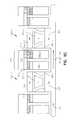
- FIG. 1Afloating gate (FIG. 1A) materials is provided in U.S. Pat. No. 5,801,401 by L. Forbes, entitled “FLASH MEMORY WITH MICROCRYSTALLINE SILICON CARBIDE AS THE FLOATING GATE STRUCTURE.” Another example is provided in U.S. Pat. No. 5,852,306 by L. Forbes, entitled “FLASH MEMORY WITH NANOCRYSTALLINE SILICON FILM AS THE FLOATING GATE.” Still further examples of this approach are provided in pending applications by L. Forbes and K.
- FIG. 1BAn example of the use of the structured surface approach (FIG. 1B) is provided in U.S. Pat. No. 5,981,350 by J. Geusic, L. Forbes, and K. Y. Ahn, entitled “DRAM CELLS WITH A STRUCTURE SURFACE USING A SELF STRUCTURED MASK.” Another example is provided in U.S. Pat. No. 6,025, 627 by L. Forbes and J. Geusic, entitled “ATOMIC LAYER EXPITAXY GATE INSULATORS AND TEXTURED SURFACES FOR LOW VOLTAGE FLASH MEMORIES.”
- FIG. 1Camorphous SiC gate insulators
- graded composition insulatorshave been described by the same inventors, formed of silicon suboxide and silicon oxycarbide in combination with an SiO2 layer, to increase the tunneling probability and reduce erase time.
- graded composition insulatorshave been described by the same inventors, formed of silicon suboxide and silicon oxycarbide in combination with an SiO2 layer, to increase the tunneling probability and reduce erase time.
- a non-volatile memory cellincludes a first source/drain region and a second source/drain region separated by a channel region in a substrate.
- a floating gateopposes the channel region and is separated therefrom by a gate oxide.
- a control gateopposes the floating gate and is separated from the floating gate by a compositionally graded mixed metal oxide tunnel barrier intergate insulator.
- the intergate insulatoris produced by low temperature chemical vapor deposition using a mixture of TiO 2 -ZrO 2 .
- the intergate insulatoris produced by low temperature chemical vapor deposition using a mixture of TiO 2 -HfO 2 .
- the intergate insulatoris produced by low temperature chemical vapor deposition using a mixture of ZrO 2 -HfO 2 . In another embodiment, the intergate insulator is produced by low temperature chemical vapor deposition using a mixture of TiO 2 -ZrO 2 -HfO 2 . In another embodiment, intergate insulator is produced by a sequential atomic layer deposition process to make a graded Al 2 O 3 -SiO 2 mixed oxide barrier oxide. Here, the sequential atomic layer deposition produces a larger number of alumina mono-layers, interspersed with a lesser number of silica mono-layers, in the region nearest to the floating gate. In another embodiment, the intergate insulator is produced by oxidation of metal alloy films containing transition metals.
- FIGS. 1 A- 1 Cillustrate a number of previous methods for reducing tunneling barriers in Flash memory.
- FIG. 2illustrates one embodiment of a floating gate transistor, or non-volatile memory cell, according to the teachings of the present invention.
- FIG. 3illustrates another embodiment of a floating gate transistor, or non-volatile memory cell, according to the teachings of the present invention.
- FIG. 4is a perspective view illustrating an array of silicon pillars formed on a substrate as used in one embodiment according to the teachings of the present invention.
- FIGS. 5 A- 5 Eare cross sectional views taken along cut line 5 - 5 from FIG. 4 illustrating a number of floating gate and control gate configurations which are included in the scope of the present invention.
- FIGS. 6 A- 6 Dillustrate a number of address coincidence schemes can be used together with the present invention.
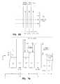
- FIG. 7Ais an energy band diagram illustrating the band structure at vacuum level with the low tunnel barrier interpoly insulator according to the teachings of the present invention.
- FIG. 7Bis an energy band diagram illustrating the band structure during an erase operation of electrons from the floating gate to the control gate across the low tunnel barrier interpoly insulator according to the teachings of the present invention.
- FIG. 7Cis a graph plotting tunneling currents versus the applied electric fields (reciprocal applied electric field shown) for an number of barrier heights.
- FIG. 8illustrates an energy band diagram useful in describing the properties of an embodiment of the present invention.
- FIG. 9is a table which provides relevant data on the barrier heights, energy gaps, dielectric constants and electron affinities of a wide variety of metal oxides that could be used as asymmetric tunnel barriers according to the teachings of the present invention.
- FIGS. 10 A- 10 Billustrate different embodiments for the compositional profiles for the graded composition metal oxide tunnel barrier intergate insulators according to the teachings of the present invention.
- FIG. 11illustrates a block diagram of an embodiment of an electronic system according to the teachings of the present invention.
- FIG. 12is a schematic diagram illustrating a conventional NOR-NOR programmable logic array.
- FIG. 13is a schematic diagram illustrating generally an architecture of one embodiment of a novel in-service programmable logic array (PLA) with floating gate transistors, or logic cells, having graded metal oxide tunnel barrier interpoly insulators according to the teachings of the present invention.
- PLAprogrammable logic array
- FIG. 14is a simplified block diagram of a high-level organization of an electronic system according to the teachings of the present invention.
- wafer and substrateare interchangeably used to refer generally to any structure on which integrated circuits are formed, and also to such structures during various stages of integrated circuit fabrication. Both terms include doped and undoped semiconductors, epitaxial layers of a semiconductor on a supporting semiconductor or insulating material, combinations of such layers, as well as other such structures that are known in the art.
- the term “horizontal” as used in this applicationis defined as a plane parallel to the conventional plane or surface of a wafer or substrate, regardless of the orientation of the wafer or substrate.
- the term “vertical”refers to a direction perpendicular to the horizontal as defined above. Prepositions, such as “on”, “side” (as in “sidewall”), “higher”, “lower”, “over” and “under” are defined with respect to the conventional plane or surface being on the top surface of the wafer or substrate, regardless of the orientation of the wafer or substrate.
- the present inventiondescribes the use of graded composition metal oxide inter-poly dielectric insulators between the control gate and the floating gate of non-volatile memory cells.
- An exampleis shown in FIG. 2 for a planar structure, or horizontal non-volatile memory cell.
- This non-volatile memory cell, as described herein,can then be implemented in a number of programmable array type logic and/or memory devices according to the teachings of the present invention.
- the use of a graded composition metal oxide films for this purposeoffer a number of advantages including:
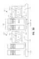
- FIG. 2illustrates one embodiment of a floating gate transistor, or non-volatile memory cell 200 , according to the teachings of the present invention.
- the non-volatile memory cell 200includes a first source/drain region 201 and a second source/drain region 203 separated by a channel region 205 in a substrate 206 .
- a floating gate 209opposes the channel region 205 and is separated therefrom by a gate oxide 211 .
- a control gate 213opposes the floating gate 209 .
- the control gate 213is separated from the floating gate 209 by a graded composition metal oxide tunnel barrier intergate insulator 215 .
- the graded composition metal oxide tunnel barrier intergate insulator 215includes a graded composition metal oxide insulator which is produced by low temperature chemical vapor deposition using a mixture of TiO 2 -ZrO 2 .
- the graded composition metal oxide tunnel barrier intergate insulator 215includes a graded composition metal oxide insulator which is produced by low temperature chemical vapor deposition using a mixture of TiO 2 -HfO 2 .
- the graded composition metal oxide tunnel barrier intergate insulator 215includes a graded composition metal oxide insulator which is produced by low temperature chemical vapor deposition using a mixture of ZrO 2 -HfO 2 .
- the graded composition metal oxide tunnel barrier intergate insulator 215includes a graded composition metal oxide insulator which is produced by low temperature chemical vapor deposition using a mixture of TiO 2 -ZrO 2 -HfO 2 .
- the graded composition metal oxide tunnel barrier intergate insulator 215includes a graded composition metal oxide insulator which is produced by a sequential atomic layer deposition process to make a graded Al 2 O 3 -SiO 2 mixed oxide barrier oxide.
- the sequential atomic layer depositionproduces a larger number of alumina mono-layers, interspersed with a lesser number of silica mono-layers, in the region nearest to the floating gate.
- the graded composition metal oxide tunnel barrier intergate insulator 215includes a graded composition metal oxide insulator which is produced by oxidation of metal alloy films containing transition metals.
- the floating gate 209includes a polysilicon floating gate 209 having a metal layer 216 formed thereon in contact with the graded composition metal oxide tunnel barrier intergate insulator 215 .
- the control gate 213includes a polysilicon control gate 213 having a metal layer 217 .
- the metal layer 217has a work function different from the metal layer 216 formed on the floating gate 209 , formed thereon in contact with the graded composition metal oxide tunnel barrier intergate insulator 215 .
- metal layer 216is formed of the same metal material used to form the graded composition metal oxide interpoly insulator 215 .
- the non-volatile memory cellas described herein, can then be implemented in a number of programmable array type logic and/or memory devices according to the teachings of the present invention.
- FIG. 3illustrates another embodiment of a floating gate transistor, or non-volatile memory cell 300 , according to the teachings of the present invention.
- the non-volatile memory cell 300includes a vertical non volatile memory cell 300 .
- the non-volatile memory cell 300has a first source/drain region 301 formed on a substrate 306 .
- a body region 307 including a channel region 305is formed on the first source/drain region 301 .
- a second source/drain region 303is formed on the body region 307 .
- a floating gate 309opposes the channel region 305 and is separated therefrom by a gate oxide 311 .
- a control gate 313opposes the floating gate 309 . According to the teachings of the present invention, the control gate 313 is separated from the floating gate 309 by a graded composition metal oxide tunnel barrier intergate insulator 315 .
- the graded composition metal oxide tunnel barrier intergate insulator 315includes a graded composition metal oxide insulator which is produced by low temperature chemical vapor deposition using a mixture of TiO 2 -ZrO 2 .
- the graded composition metal oxide tunnel barrier intergate insulator 315includes a graded composition metal oxide insulator which is produced by low temperature chemical vapor deposition using a mixture of TiO 2 -HfO 2 .
- the graded composition metal oxide tunnel barrier intergate insulator 315includes a graded composition metal oxide insulator which is produced by low temperature chemical vapor deposition using a mixture of ZrO 2 -HfO 2 .
- the graded composition metal oxide tunnel barrier intergate insulator 315includes a graded composition metal oxide insulator which is produced by low temperature chemical vapor deposition using a mixture of TiO 2 -ZrO 2 -HfO 2 .
- the graded composition metal oxide tunnel barrier intergate insulator 315includes a graded composition metal oxide insulator which is produced by a sequential atomic layer deposition process to make a graded Al 2 O 3 -SiO 2 mixed oxide barrier oxide.
- the sequential atomic layer depositionproduces a larger number of alumina mono-layers, interspersed with a lesser number of silica mono-layers, in the region nearest to the floating gate.
- the graded composition metal oxide tunnel barrier intergate insulator 315includes a graded composition metal oxide insulator which is produced by oxidation of metal alloy films containing transition metals.
- the floating gate 309includes a polysilicon floating gate 309 having a metal layer 316 formed thereon in contact with the graded composition metal oxide tunnel barrier intergate insulator 315 .
- the control gate 313includes a polysilicon control gate 313 having a metal layer 317 .
- the metal layer 317has a work function different from the metal layer 316 formed on the floating gate 309 , formed thereon in contact with the graded composition metal oxide tunnel barrier intergate insulator 315 .
- the non-volatile memory cellas described herein, can then be implemented in a number of programmable array type logic and/or memory devices according to the teachings of the present invention.
- the floating gate 309includes a vertical floating gate 309 formed alongside of the body region 307 .
- the control gate 313includes a vertical control gate 313 formed alongside of the vertical floating gate 309 .
- the control gate 313is separated from the floating gate 309 by a graded composition metal oxide tunnel barrier intergate insulator 315 .
- the floating gate 309 and control gate 313 orientation shown in FIG. 3is just one embodiment for a vertical non volatile memory cell 300 , according to the teachings of the present invention.
- the floating gateincludes a horizontally oriented floating gate formed alongside of the body region.
- the control gateincludes a horizontally oriented control gate formed above the horizontally oriented floating gate.
- FIG. 4is a perspective view illustrating an array of silicon pillars 400 - 1 , 400 - 2 , 400 - 3 , . . . , 400 -N, formed on a substrate 406 as used in one embodiment according to the teachings of the present invention.
- the substratescan be (i) conventional p-type bulk silicon or p-type epitaxial layers on p+ wafers, (ii) silicon on insulator formed by conventional SIMOX, wafer bonding and etch back or silicon on sapphire, or (iii) small islands of silicon on insulator utilizing techniques such as described in more detail in U.S. Pat. No. 5,691,230, by Leonard Forbes, entitled “Technique for Producing Small Islands of Silicon on Insulator,” issued Nov. 25, 1997, which is incorporated herein by reference.
- each pillar in the array of silicon pillars 400 - 1 , 400 - 2 , 400 - 3 , . . . , 400 -Nincludes a first source/drain region 401 and a second source/drain region 403 .
- the first and the second source/drain regions, 401 and 403are separated by a body region 407 including channel regions 405 .
- a number of trenches 430separate adjacent pillars in the array of silicon pillars 400 - 1 , 400 - 2 , 400 - 3 , . . . , 400 -N.
- Trenches 430are referenced in connection with the discussion which follows in connection with FIGS. 5 A- 5 E.
- FIGS. 5 A- 5 Eare cross sectional views taken along cut line 5 - 5 from FIG. 4. As mentioned above in connection with FIG. 3, a number of floating gate and control gate configurations are included in the present invention.
- FIG. 5Aillustrates one such embodiment of the present invention.
- FIG. 5Aillustrates a first source/drain region 501 and second source/drain region 503 for a non-volatile memory cell 500 formed according to the teachings of the present invention.
- the first and second source/drain regions, 501 and 503are contained in a pillar of semiconductor material, and separated by a body region 507 including channel regions 505 .
- FIGS. 5 A- 5 Eare cross sectional views taken along cut line 5 - 5 from FIG. 4.
- FIG. 5Aillustrates one such embodiment of the present invention.
- FIG. 5Aillustrates a first source/drain region 501 and second source/drain region 503 for a non-volatile memory cell 500 formed according to the teachings of the present invention.
- the first source/drain region 501is integrally connected to a buried sourceline 525 .
- the buried sourceline 525is be formed of semiconductor material which has the same doping type as the first source/drain region 501 .
- the sourceline 525is formed of semiconductor material of the same doping as the first source/drain region 501 , but is more heavily doped than the first source/drain region 501 .
- a pair of floating gates 509 - 1 and 509 - 2are formed in each trench 530 between adjacent pillars which form memory cells 500 - 1 and 500 - 2 .
- Each one of the pair of floating gates, 509 - 1 and 509 - 2respectively opposes the body regions 507 - 1 and 507 - 2 in adjacent pillars 500 - 1 and 500 - 2 on opposing sides of the trench 530 .
- a single control gate 513is shared by the pair of floating gates 509 - 1 and 509 - 2 on opposing sides of the trench 530 .
- the shared single control gate 513can include an integrally formed control gate line.
- an integrally formed control gate line 513can be one of a plurality of control gate lines which are each independently formed in the trench, such as trench 530 , below the top surface of the pillars 500 - 1 and 500 - 2 and between the pair of floating gates 509 - 1 and 509 - 2 .
- each floating gatee.g. 509 - 1 and. 509 - 2 , includes a vertically oriented floating gate having a vertical length of less than 100 nanometers.
- a pair of floating gates 509 - 1 and 509 - 2are formed in each trench 530 between adjacent pillars which form memory cells 500 - 1 and 500 - 2 .
- Each one of the pair of floating gates, 509 - 1 and 509 - 2respectively opposes the body regions 507 - 1 and 507 - 2 in adjacent pillars 500 - 1 and 500 - 2 on opposing sides of the trench 530 .
- a plurality of control gate linesare again formed in trenches, e.g. trench 530 , below the top surface of the pillars, 500 - 1 and 500 - 2 , and between the pair of floating gates 509 - 1 and 509 - 2 .
- each trenche.g. 530
- Each one of the pair of control gate lines 513 - 1 and 513 - 2addresses the floating gates, 509 - 1 and 509 - 2 respectively, on opposing sides of the trench 530 .
- the pair of control gate lines, or control gates 513 - 1 and 513 - 2are separated by an insulator layer.
- a pair of floating gates 509 - 1 and 509 - 2are again formed in each trench 530 between adjacent pillars which form memory cells 500 - 1 and 500 - 2 .
- Each one of the pair of floating gates, 509 - 1 and 509 - 2respectively opposes the body regions 507 - 1 and 507 - 2 in adjacent pillars 500 - 1 and 500 - 2 on opposing sides of the trench 530 .
- the plurality of control gate linesare disposed vertically above the floating gates. That is, in one embodiment, the control gate lines are located above the pair of floating gates 509 - 1 and 509 - 2 and not fully beneath the top surface of the pillars 500 - 1 and 500 - 2 . In the embodiment of FIG. 5C, each pair of floating gates, e.g. 509 - 1 and 509 - 2 , in a given trench shares a single control gate line, or control gate 513 .
- a pair of floating gates 509 - 1 and 509 - 2are formed in each trench 530 between adjacent pillars which form memory cells 500 - 1 and 500 - 2 .
- Each one of the pair of floating gates, 509 - 1 and 509 - 2respectively opposes the body regions 507 - 1 and 507 - 2 in adjacent pillars 500 - 1 and 500 - 2 on opposing sides of the trench 530 .
- the plurality of control gate linesare disposed vertically above the floating gates. That is, in one embodiment, the control gate lines are located above the pair of floating gates 509 - 1 and 509 - 2 and not fully beneath the top surface of the pillars 500 - 1 and 500 - 2 . However, in the embodiment of FIG. 5D, each one of the pair of floating gates, e.g. 509 - 1 and 509 - 2 , is addressed by an independent one of the plurality of control lines or control gates, shown in FIG. 5D as 513 - 1 and 513 - 2 .
- a single floating gate 509is formed in each trench 530 between adjacent pillars which form memory cells 500 - 1 and 500 - 2 .
- the single floating gate 509can be either a vertically oriented floating gate 509 or a horizontally oriented floating gate 509 formed by conventional processing techniques, or can be a horizontally oriented floating gate 509 formed by a replacement gate technique such as described in a copending application, entitled “Flash Memory with Ultrathin Vertical Body Transistors,” by Leonard Forbes and Kie Y. Ahn, application Ser. No. 09/780,169.
- the floating gate 509has a vertical length facing the body region 505 of less than 100 nm. In another embodiment, the floating gate 509 has a vertical length facing the body region 505 of less than 50 nm. In one embodiment, as shown in FIG. 5E, the floating gate 509 is shared, respectively, with the body regions 507 - 1 and 507 - 2 , including channel regions 505 - 1 and 505 - 2 , in adjacent pillars 500 - 1 and 500 - 2 located on opposing sides of the trench 530 . In one embodiment, the control gate 513 includes a horizontally oriented control gate 513 formed above the horizontally oriented floating gate 509 .
- the floating gates 509are separated from the control gate lines, or control gates 513 with a graded composition metal oxide tunnel barrier intergate insulator in accordance with the descriptions given above in connection with FIG. 3.
- the modifications hereare to use tunneling through the interpoly dielectric to realize flash memory devices.
- the vertical devicesinclude an extra flexibility in that the capacitors, e.g. gate oxide and intergate insulator, are easily fabricated with different areas. This readily allows the use of very high dielectric constant inter-poly dielectric insulators with lower tunneling barriers.
- FIGS. 6 A- 6 Dillustrate that a number of address coincidence schemes can be used together with the present invention.
- FIG. 6Aillustrates a NOR flash memory array 610 having a number of non-volatile memory cells 600 - 1 , 600 - 2 , 600 - 3 , using a coincidence address array scheme.
- FIG. 6Ashows a sourceline 625 coupled to a first source/drain region 601 in each of the number of non-volatile memory cells 600 - 1 , 600 - 2 , 600 - 3 .
- the sourcelineis shown oriented in a first selected direction in the flash memory array 610 .
- FIG. 6Aa number of control gate lines 630 are shown oriented in a second selected direction in the flash memory array 610 .
- the number of control gate lines 630are coupled to, or integrally formed with the control gates 613 for the number of non-volatile memory cells 600 - 1 , 600 - 2 , 600 - 3 .
- the second selected directionis orthogonal to the first selected direction.
- FIG. 6Ashows a number of bitlines 635 oriented in a third selected direction in the flash memory array 610 . As shown in FIG.
- the number of bitlinesare coupled to the second source/drain regions in the number of non-volatile memory cells 600 - 1 , 600 - 2 , 600 - 3 .
- the third selected directionis parallel to the second selected direction and the number of control gate lines 630 serve as address lines.
- the flash memory array 610includes a number of backgate or substrate/well bias address lines 640 coupled to the substrate.
- FIGS. 6 B- 6 Dillustrate of top view for three different coincidence address scheme layouts suitable for use with the present invention.
- FIG. 6Bprovides the top view layout of the coincidence address scheme described in connection with FIG. 6A. That is, FIG. 6B illustrates a number of sourcelines 625 oriented in a first selected direction, a number of control gate lines 630 oriented in a second selected direction, and a number of bitlines 635 oriented in a third selected direction for the flash memory array 600 .
- the second and third selected directionare parallel to one another and orthogonal to the first selected direction such that the number of control gate lines 630 serve as address lines.
- FIG. 6Cprovides the top view layout of another coincidence address scheme according to the teachings of the present invention.
- FIG. 6Cillustrates a number of sourcelines 625 oriented in a first selected direction, a number of control gate lines 630 oriented in a second selected direction, and a number of bitlines 635 oriented in a third selected direction for the flash memory array 600 .
- the first selected direction and the third selected directionare parallel to one another and orthogonal to the second selected direction.
- the number of control gate lines 630again serve as address lines.
- FIG. 6Dprovides the top view layout of yet another coincidence address scheme according to the teachings of the present invention.
- FIG. 6Dillustrates a number of sourcelines 625 oriented in a first selected direction, a number of control gate lines 630 oriented in a second selected direction, and a number of bitlines 635 oriented in a third selected direction for the flash memory array 600 .
- the first selected direction and the second selected directionare parallel to one another and orthogonal to the third selected direction.
- the number of bitlines 635serve as address lines.
- writecan still be achieved by hot electron injection and/or, according to the teachings of the present invention, tunneling from the control gate to the floating gate.
- block eraseis accomplished by driving the control gates with a relatively large positive voltage and tunneling from the metal on top of the floating gate to the metal on the bottom of the control gate.
- FIG. 7Ais an energy band diagram illustrating the band structure at vacuum level with the graded composition metal oxide tunnel barrier interpoly insulator according to the teachings of the present invention.
- FIG. 7Ais useful in illustrating the reduced tunnel barrier off of the floating gate to the control gate and for illustrating the respective capacitances of the structure according to the teachings of the present invention.
- FIG. 7Ashows the graded composition metal oxide tunnel barriers, formed by low temperature CVD, by low temperature oxidation of metal alloy films, and by atomic layer deposition (ALD), as used in the present invention for easy erase. Erase is achieved by the use of positive control gate voltages through the low tunnel barrier.
- readutilizes positive control gate voltages with n-channel enhancement mode devices as described in the above referenced, copending applications, by the same inventors, entitled “FLASH MEMORY DEVICES WITH METAL OXIDE AND/OR LOW TUNNEL BARRIER INTERPLOY INSULATORS,” attorney docket number 1303.014US1, application Ser. No.
- readutilizes negative control gate voltages with n-channel depletion mode devices as described in the above referenced, copending application, by the same inventors, entitled “PROGRAMMABLE ARRAY TYPE LOGIC AND/OR MEMORY DEVICES WITH METAL OXIDE AND/OR LOW ASYMMETRICAL TUNNEL BARRIER INTERPLOY INSULATORS,” attorney docket number 1303.020US1, application Ser. No. 09/943,134.
- readutilizes negative control gate voltages with p-channel enhancement mode devices as described in the above referenced, copending application, by the same inventors, entitled “PROGRAMMABLE ARRAY TYPE LOGIC OR MEMORY WITH P-CHANNEL DEVICES AND ASYMMETRICAL TUNNEL BARRIERS,” attorney docket number 1303.035US1, application Ser. No. 10/028,001.
- Programmingis accomplished by channel hot electron injection with n-channel devices and/or electron injection from the control gate for both n-channel and p-channel devices and may or may not utilize positive substrate, well, or body bias.
- FIG. 7Bis an energy band diagram illustrating the band structure during an erase operation of electrons from the floating gate 705 to the control gate 713 across the graded composition metal oxide tunnel barrier interpoly insulator 707 according to the teachings of the present invention.
- FIG. 7Bis similarly useful in illustrating the reduced tunnel barrier off of the floating gate 705 to the control gate 713 and for illustrating the respective capacitances of the structure according to the teachings of the present invention.
- the electric fieldis determined by the total voltage difference across the structure, the ratio of the capacitances (see FIG. 7A), and the thickness of the graded composition interpoly dielectric 707 .
- Eis the electric field across the interpoly dielectric insulator 707 and Eo depends on the barrier height.
- the lower electric field in the aluminum oxide interpoly insulator 707 for the same current densityreflects the lower tunneling barrier of approximately 2 eV, shown in FIG. 7B, as opposed to the 3.2 eV tunneling barrier of silicon oxide 703 , also illustrated in FIG. 7B.
- FIG. 7Cis a graph plotting tunneling currents versus the applied electric fields (reciprocal applied electric field shown) for a number of barrier heights.
- FIG. 7Cillustrates the dependence of the tunneling currents on electric field (reciprocal applied electric field) and barrier height.
- the fraction of voltage across the graded composition interpoly or graded composition intergate insulator, ⁇ V 2can be increased by making the area of the intergate capacitor, C 2 , (e.g. intergate insulator 707 ) smaller than the area of the transistor gate capacitor, C 1 (e.g. gate oxide 703 ). This would be required with high dielectric constant intergate dielectric insulators 707 and is easily realized with the vertical floating gate structures described above in connection with FIGS. 3 , and 5 A- 5 E.
- barrier heights for Pt/TiO 2 and Pt/Ta 2 O 5are ⁇ 1.2 and 2.0, respectively.
- a barrier(comprised in part of TiO 2 and the remainder is Ta 2 O 5 ) that is Ti-rich at the inner interface but less so at the outer will have an asymmetrical barrier that is lower at the inner and higher at the outer interface for the same (Pt) contact metal.
- Experimental barrier heightshave not been determined for even homogeneous mixed oxide layers.
- barrier heightsby assuming that they will be intermediate between those of the component oxides.
- a mixed oxide comprised of equal amounts of TiO 2 and Ta 2 O 5should have a barrier height near ⁇ 1.6 eV with a Pt contact.
- the present inventiondiscloses how to form asymmetrical, mixed oxide tunnel barrier structures using a variety of oxides and practical processes. Although not discussed, it is quite clear that some of these processes can also be employed to produce graded tunnel barriers comprised of other insulating materials including oxy-nitrides, nitrides and possibly oxy-carbides and even carbides.
- Process 1Deposit a layer of Al on the floating gate to provide a planar, A. conducting surface. 2. Deposit a layer of Ti—Zr alloy. 3. Deposit a TiO 2 —ZrO 2 film using a modified process such as that described in the above article by Smith et al.
- a relative concentration- distance profileis shown schematically after oxide formation in FIG. 10A. The outer barrier will be greater than the inner. 4.
- Process 1.Deposit a layer Al on the Si floating gate. This serves as an B.
- Process 1Modify the graded mixed oxides produced above in order to C. stabilized their as-deposited structure and prevent unwanted crystallization and grain grown. This can be done with small additions of glass-forming elements to the anhydrous metal nitrate reactants. For silicon, this might involve using a volatile halide compound since Si does not form nitrates or nitrides.
- the present inventiondiscloses the novel concept of forming and oxidizing graded-composition, metal allow films for producing graded composition oxide tunnel barriers.
- the present inventionuses for this purpose alloy films that typically contain Transition Metals (TM's) having important, common characteristics: 1) TM's mainly oxidize with a logarithmic-type time dependence, reaching self-limiting oxide thickness values (under 100 ⁇ ) in oxygen for temperatures ⁇ 400 degrees Celsius. 2) The TM's are refractory with very small diffusivities at low temperatures. Thus one can make TM alloy films having concentration gradients that are stable, provided the films are not heated excessively prior to oxidation. 3) Most TM's including lanthanides and alkaline earth metal possess very high and relatively similar affinities for oxygen.
- TM'sTransition Metals
- TM oxides formed by oxidation at low temperaturesare amorphous or virtually so.
- experimental data on low temperature oxidation of TM alloysis non-existent or nearly so.
- those skilled in the artcan a priori choose particular TM alloy films that will obey logarithmic—time growth dependencies, thus allowing for the production of mixed oxide layers having highly-determinable thicknesses.
- the relative concentrations of TM's in the growing oxidewill correspond to those being converted to oxide in the underlying alloy. Thus graded composition oxides can be produced reproducibly.
- the mixed TM oxides thus producedwill be amorphous or nearly so.
- Processes D to Fare given as examples.
- Process 1.Deposit an Al layer on the Si floating gate.
- D. 2.Deposit a thin layer of Pt or Pd.
- 3.Deposit a Ti—Zr alloy film having a Zr/Ti concentration ratio which increases with thickness. Films can be made using: co- deposition with 2 Knudsen evaporation sources having fluxes programmed to vary with film thickness; co-deposition from 2 sputter guns; possibly by physical sputtering a single target, varying sputtering parameters with time. 4.
- Graded Oxide Barriers by ALDcan produce a large number of mixed oxide tunnel barriers.
- Kukli et alhave formed graded mixtures of Ta 2 O 5 , Nb 2 O 5 and Al 2 O 3 by ALD on soda lime substrates at 300 degrees Celsius, using precursors of Ta(OC 2 H 5 ) 5 , Nb(OC 2 H 5 ) 5 and AlCl 3 and well established ALD recipes.
- K. Kukli et al“Development of Dielectric Properties of Niobium Oxide, Tantalum Oxide and Aluminum Oxide Based Nanolayer Materials,” J. Electrochecm. Soc. Vol. 148 (2), F35-F41 (2001)).
- the sequencingwill be such as to produce a larger number of alumina mono-layers, interspersed with a lesser number of silica mono-layers, in the region nearest to an inner interface with the floating gate.
- the sequencingwill be such as to produce a larger number of alumina mono-layers, interspersed with a lesser number of silica mono-layers, in the region nearest to an inner interface with the floating gate.
- With increasing thickness of the nano-laminateprogressively increase the number of silica layers deposited, relative to the number of alumina layers. For example, one might have a sequence such as:
- F.G. and C.G.represent the Floating Gate and Control Gate contacts, respectively.
- the barrier height of the alumina-rich regionwill be mitigated by the close proximity of silica while the silica-rich barrier will be lowered due to the presence of alumina 2 mono-layers distant from the C.G.
- the relative influence on the effective tunnel barrier of a given “doping” layerwill diminish rapidly with its distance from the electrode. Nevertheless one can certainly produce asymmetrical barriers in this fashion, with the ability to fine-tune the relative heights of each. It is also clear that other symmetrical tunnel barriers can be formed using other ALD oxides.
- Writecan be achieved by tunneling from the control gate to the floating gate by driving the control gate negative and/or channel hot electron injection as in conventional flash memory devices. Erase would be accomplished by driving the control gates with a relatively large positive voltage and tunneling from the metal on top of the floating gate to the metal on the bottom of the control gate through the graded composition metal oxide tunnel barrier intergate insulators of the present invention. A graded composition metal oxide tunnel barrier between the floating gate and the control gate will make the erase operation easy.
- n-channel enhancement mode devicesare used in the array, reading is accomplished by driving the control gate with a smaller positive voltage. If no electrons are stored on the floating gate the transistor will turn on. If electrons are stored on the floating gate the transistor will not turn on or only turn on at a lower conductivity state. This constitutes the memory function. If n-channel depletion mode devices are used in the array then reading of the stored data is accomplished with a zero or negative gate voltage, if the device conducts with zero or negative small gate voltage then there is no charge stored on the floating gate. If the floating gate is charged by stored electrons then the transistor will not conduct with zero or low negative gate voltages.
- the presence of stored charge on the floating gate and/or applied negative gate voltageswill result in electric fields in the interpoly/intergate insulator. If the gate oxide is 2 nm (20 ⁇ ) thick then the capacitance is about 1.6 ⁇ 10 ⁇ 6 F/cm 2 and a 1 Volt difference will store a charge of 1.6 ⁇ 10 ⁇ 6 Coulombs/cm 2 . A retention time of one second requires a leakage current of less than about 10 ⁇ 6 Amps/cm 2 , if as shown in FIG.
- the tunneling barrieris 2.0 eV and the electric field in the interpoly/intergate insulator is less than about 2 ⁇ 10 6 V/cm then the current density will be 10 ⁇ 16 Amps/cm 2 and the retention time 10 +10 seconds.
- One yearis about 3 ⁇ 10 +7 seconds, very long retention times can be achieved by using low electric fields during read in conjunction with the larger tunnel barrier during read.
- the lower tunneling barrierresults in a much faster erase at much lower electric fields and than in conventional flash memory devices which require fields of 10 7 V/cm to achieve the erase currents of 1 Amp/cm 2 with a silicon oxide tunnel barrier of 3.2 eV.
- the graded composition tunnel barriers of the present inventioncan serve to make erase of flash memory type devices easy while insuring a long retention time during standby and read operations.
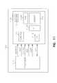
- FIG. 11illustrates a block diagram of an embodiment of an electronic system 1101 according to the teachings of the present invention.
- the system 1101includes a memory device 1100 which has an array of memory cells 1102 , address decoder 1104 , row access circuitry 1106 , column access circuitry 1108 , control circuitry 1110 , and input/output circuit 1112 .
- the circuit 1101includes a processor 1114 , or memory controller for memory accessing.
- the memory device 1100receives control signals from the processor 1114 , such as WE*, RAS* and CAS* signals over wiring or metallization lines.
- the memory device 1100is used to store data which is accessed via I/O lines.
- At least one of the processor 1114 or memory device 1100has a memory cell formed according to the embodiments of the present invention. That is, at least one of the processor 1114 or memory device 1100 includes a graded composition metal oxide tunnel barrier interpoly insulator according to the teachings of the present invention.
- FIG. 11illustrates an embodiment for electronic system circuitry in which the novel memory cells of the present invention are used.
- the illustration of system 1101is intended to provide a general understanding of one application for the structure and circuitry of the present invention, and is not intended to serve as a complete description of all the elements and features of an electronic system using the novel memory cell structures.
- the inventionis equally applicable to any size and type of memory device 1100 using the novel memory cells of the present invention and is not intended to be limited to that described above.
- such an electronic systemcan be fabricated in single-package processing units, or even on a single semiconductor chip, in order to reduce the communication time between the processor and the memory device.
- Applications containing the novel memory cell of the present invention as described in this disclosureinclude electronic systems for use in memory modules, device drivers, power modules, communication modems, processor modules, and application-specific modules, and may include multilayer, multichip modules.
- Such circuitrycan further be a subcomponent of a variety of electronic systems, such as a clock, a television, a cell phone, a personal computer, an automobile, an industrial control system, an aircraft, and others.
- FIG. 12shows a conventional NOR-NOR logic array 1200 which is programmable at the gate mask level by either fabricating a thin oxide gate transistor, e.g. logic cells 1201 - 1 , 1201 - 2 , . . . , 1201 -N and 1203 - 1 , 1203 - 2 , . . . , 1203 -N, at the intersection of lines in the array or not fabricating a thin oxide gate transistor, e.g. missing thin oxide transistors, 1202 - 1 , 1202 - 2 , . . . , 1202 -N, at such an intersection.
- a thin oxide gate transistore.g. logic cells 1201 - 1 , 1201 - 2 , . . . , 1201 -N and 1203 - 1 , 1203 - 2 , . . . , 1203 -N, at such an intersection.
- NMOS transistors1216 and 1218 respectively, are used as load devices.
- the conventional logic array shown in FIG. 12includes a first logic plane 1210 which receives a number of input signals at input lines 1212 .
- first logic plane 1210can include inverters to produce the complementary signals when needed in a specific application.
- First logic plane 1210includes a number of thin oxide gate transistors, e.g. transistors 1201 - 1 , 1201 - 2 , . . . , 1201 -N.
- the thin oxide gate transistors, 1201 - 1 , 1201 - 2 , . . . , 1201 -Nare located at the intersection of input lines 1212 , and interconnect lines 1214 .
- this selective fabrication of thin oxide gate transistore.g. transistors 1201 - 1 , 1201 - 2 , . . .
- 1201 -Nis referred to as programming since the logical function implemented by the programmable logic array is entered into the array by the selective arrangement of the thin oxide gate transistors, or logic cells, 1201 - 1 , 1201 - 2 , . . . , 1201 -N, at the intersections of input lines 1212 , and interconnect lines 1214 in the array.
- each of the interconnect lines 1214acts as a NOR gate for the input lines 1212 that are connected to the interconnect lines 1214 through the thin oxide gate transistors, 1201 - 1 , 1201 - 2 , . . . , 1201 -N, of the array.
- interconnection line 1214 Aacts as a NOR gate for the signals on input lines 1212 A and 1212 B. That is, interconnect line 1214 A is maintained at a high potential unless one or more of the thin oxide gate transistors, 1201 - 1 , 1201 - 2 , . . .
- each thin oxide gate transistore.g. transistors 1201 - 1 , 1201 - 2 , . . . , 1201 -N, conducts which performs the NOR positive logic circuit function, an inversion of the OR circuit function results from inversion of data onto the interconnect lines 1214 through the thin oxide gate transistors, 1201 - 1 , 1201 - 2 , . . . , 1201 -N, of the array.
- a second logic plane 1224which includes a number of thin oxide gate transistor, e.g. transistors 1203 - 1 , 1203 - 2 , . . . , 1203 -N.
- the thin oxide gate transistors, 1203 - 1 , 1203 - 2 , . . . , 1203 -N,are located at the intersection of interconnect lines 1214 , and output lines 1220 .
- the logical function of the second logic plane 1224is implemented by the selective arrangement of the thin oxide gate transistors, 1203 - 1 , 1203 - 2 , . . .
- the second logic plane 1224is also configured such that the output lines 1220 comprise a logical NOR function of the signals from the interconnection lines 1214 that are coupled to particular output lines 1220 through the thin oxide gate transistors, 1203 - 1 , 1203 - 2 , . . . , 1203 -N, of the second logic plane 1224 .
- the incoming signals on each lineare used to drive the gates of transistors in the NOR logic array as the same is known by one of ordinary skill in the art and will be understood by reading this disclosure.
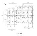
- FIG. 13illustrates an embodiment of a novel in-service programmable logic array (PLA) formed according to the teachings of the present invention.
- PLA 1300implements an illustrative logical function using a two level logic approach.
- PLA 1300includes first and second logic planes 1310 and 1322 .
- the logic functionis implemented using NOR-NOR logic.
- first and second logic planes 1310 and 1322each include an array of, logic cells, non-volatile memory cells, or floating gate driver transistors, 1301 - 1 , 1301 - 2 , . . . , 1301 -N, and 1302 - 1 , 1302 - 2 , . . .
- the floating gate driver transistors, 1301 - 1 , 1301 - 2 , . . . , 1301 -N, and 1302 - 1 , 1302 - 2 , . . . , 1302 -Nhave their first source/drain regions coupled to source lines or a conductive source plane, as shown and described in more detail in connection with FIGS. 3 and 5E.
- the floating gate driver transistors, 1301 - 1 , 1301 - 2 , . . . , 1301 -N, and 1302 - 1 , 1302 - 2 , . . . , 1302 -Nare configured to implement the logical function of FPLA 1300 .
- the floating gate driver transistors, 1301 - 1 , 1301 - 2 , . . . , 1301 -N, and 1302 - 1 , 1302 - 2 , . . . , 1302 -Nare shown as n-channel floating gate transistors. However, the invention is not so limited. Also, as shown in FIG. 13, a number of p-channel metal oxide semiconductor (PMOS) transistors are provided as load device transistors, 1316 and 1324 respectively, having their source regions coupled to a voltage potential (VDD).
- VDDvoltage potential
- load device transistors, 1316 and 1324respectively, operate in complement to the floating gate driver transistors, 1301 - 1 , 1301 - 2 , . . . , 1301 -N, and 1302 - 1 , 1302 - 2 , . . . , 1302 -N to form load inverters.
- FIG. 13is provided by way of example and not by way of limitation. Specifically, the teachings of the present application are not limited to programmable logic arrays in the NOR-NOR approach. Further, the teachings of the present application are not limited to the specific logical function shown in FIG. 13. Other logical functions can be implemented in a programmable logic array, with the floating gate driver transistors, 1301 - 1 , 1301 - 2 , . . . , 1301 -N, and 1302 - 1 , 1302 - 2 , . . . , 1302 -N and load device transistors, 1316 and 1324 respectively, of the present invention, using any one of the various two level logic approaches.
- First logic plane 1310receives a number of input signals at input lines 1312 .
- no invertersare provided for generating complements of the input signals.
- first logic plane 1310can include inverters to produce the complementary signals when needed in a specific application.
- First logic plane 1310includes a number of floating gate driver transistors, 1301 - 1 , 1301 - 2 , . . . , 1301 -N, that form an array such as an array of non-volatile memory cells, or flash memory cells.
- the floating gate driver transistors, 1301 - 1 , 1301 - 2 , . . . , 1301 -Nare located at the intersection of input lines 1312 , and interconnect lines 1314 . Not all of the floating gate driver transistors, 1301 - 1 , 1301 - 2 , . . . , 1301 -N, are operatively conductive in the first logic plane.
- the floating gate driver transistors, 1301 - 1 , 1301 - 2 , . . . , 1301 -Nare selectively programmed, as described in detail below, to respond to the input lines 1312 and change the potential of the interconnect lines 1314 so as to implement a desired logic function.
- This selective interconnectionis referred to as programming since the logical function implemented by the programmable logic array is entered into the array by the floating gate driver transistors, 1301 - 1 , 1301 - 2 , . . . , 1301 -N, that are used at the intersections of input lines 1312 , and interconnect lines 1314 in the array.
- each of the interconnect lines 1314acts as a NOR gate for the input lines 1312 that are connected to the interconnect lines 1314 through the floating gate driver transistors, 1301 - 1 , 1301 - 2 , . . . , 1301 -N, of the array 1300 .
- interconnection line 1314 Aacts as a NOR gate for the signals on input lines 1312 A, 1312 B and 1312 C.
- Programmability of the vertical floating gate driver transistors, 1301 - 1 , 1301 - 2 , . . . , 1301 -Nis achieved by charging the vertical floating gates.
- That floating gate driver transistor, 1301 - 1 , 1301 - 2 , . . . , 1301 -Nwill remain in an off state until it is reprogrammed. Applying and removing a charge to the vertical floating gates is performed by tunneling charge between the floating gate and control gates of the floating gate driver transistors, 1301 - 1 , 1301 - 2 , . . . , 1301 -N through a low tunnel barrier interpoly, or intergate insulator as described in detail above and in connection with FIGS. 2 - 7 C.
- a floating gate driver transistors, 1301 - 1 , 1301 - 2 , . . . , 1301 -N programmed in an off stateremains in that state until the charge is removed from its vertical floating gate.
- Floating gate driver transistors, 1301 - 1 , 1301 - 2 , . . . , 1301 -N not having a corresponding vertical floating gate chargedoperate in either an on state or an off state, wherein input signals received by the input lines 1312 A, 1312 B and 1312 C determine the applicable state. If any of the input lines 1312 A, 1312 B and 1312 C are turned on by input signals received by the input lines 1312 A, 1312 B and 1312 C, then a ground is provided to load device transistors 1316 . The load device transistors 1316 are attached to the interconnect lines 1314 .
- the load device transistors 1316provide a low voltage level when any one of the floating gate driver transistors, 1301 - 1 , 1301 - 2 , . . . , 1301 -N connected to the corresponding interconnect line 1314 is activated. This performs the NOR logic circuit function, an inversion of the OR circuit function results from inversion of data onto the interconnect lines 1314 through the floating gate driver transistors, 1301 - 1 , 1301 - 2 , . . . , 1301 -N of the array 1300 . When the floating gate driver transistors, 1301 - 1 , 1301 - 2 , . . .
- each of the floating gate driver transistors, 1301 - 1 , 1301 - 2 , . . . , 1301 -N described hereinare formed according to the teachings of the present invention as described in detail in connection with FIGS. 2 - 7 C.
- second logic plane 1322comprises a second array of floating gate driver transistors, 1302 - 1 , 1302 - 2 , . . . , 1302 -N that are selectively programmed to provide the second level of the two level logic needed to implement a specific logical function.
- the array of floating gate driver transistors, 1302 - 1 , 1302 - 2 , . . . , 1302 -Nis also configured such that the output lines 1320 comprise a logical NOR function of the signals from the interconnection lines 1314 that are coupled to particular output lines 1320 through the floating gate driver transistors, 1302 - 1 , 1302 - 2 , . . . , 1302 -N of the second logic plane 1322 .
- Programmability of the vertical floating gate driver transistors, 1302 - 1 , 1302 - 2 , . . . , 1302 -Nis achieved by charging the vertical floating gate.
- that floating gate driver transistor, 1302 - 1 , 1302 - 2 , . . . , 1302 -Nwill remain in an off state until it is reprogrammed.
- Applying and removing a charge to the vertical floating gatesis performed by tunneling charge between the floating gate and control gates of the floating gate driver transistors, 1301 - 1 , 1301 - 2 , . . .
- a floating gate driver transistors, 1302 - 1 , 1302 - 2 , . . . , 1302 -N programmed in an off stateremains in that state until the charge is removed from the vertical floating gate.
- Floating gate driver transistors, 1302 - 1 , 1302 - 2 , . . . , 1302 -N not having a corresponding vertical floating gate chargedoperate in either an on state or an off state, wherein signals received by the interconnect lines 1314 determine the applicable state. If any of the interconnect lines 1314 are turned on, then a ground is provided to load device transistors 1324 by applying a ground potential to the source line or conductive source plane coupled to the transistors first source/drain region as described herein.
- the load device transistors 1324are attached to the output lines 1320 .
- the load device transistors 1324provide a low voltage level when any one of the floating gate driver transistors, 1302 - 1 , 1302 - 2 , . .
- VDD voltage levelis applied to corresponding output lines 1320 for second logic plane 1322 when a load device transistor 1324 is turned on by a clock signal received at the gate of the load device transistors 1324 ( ⁇ ).
- a NOR-NOR electrically programmable logic arrayis most easily implemented utilizing the normal PLA array structure.
- Each of the floating gate driver transistors, 1302 - 1 , 1302 - 2 , . . . , 1302 -N described hereinare formed according to the teachings of the present invention as described in detail in connection with FIGS. 2 - 7 C.
- FIG. 13shows the application of the novel, non-volatile floating gate transistors with low tunnel barrier intergate insulators in a logic array. If a floating gate driver transistors, 1301 - 1 , 1301 - 2 , . . . , 1301 -N, and 1302 - 1 , 1302 - 2 , . . . , 1302 -N, is programmed with a negative charge on the vertical floating gate it is effectively removed from the array. In this manner the array logic functions can be programmed even when the circuit is in the final circuit or in the field and being used in a system.
- the absence or presence of stored charge on the floating gatesis read by addressing the input lines 1312 or control gate lines and y-column/sourcelines to form a coincidence in address at a particular floating gate.
- the control gate linewould for instance be driven positive at some voltage of 1.0 Volt and the y-column/sourceline grounded, if the floating gate is not charged with electrons then the transistor would turn on tending to hold the interconnect line on that particular row down indicating the presence of a stored “one” in the cell. If this particular floating gate is charged with stored electrons, the transistor will not turn on and the presence of a stored “zero” indicated in the cell. In this manner, data stored on a particular floating gate can be read.
- Programmingcan be achieved by hot electron injection.
- the interconnect linescoupled to the second source/drain region for the non-volatile memory cells in the first logic plane, are driven with a higher drain voltage like 2 Volts for 0.1 micron technology and the control gate line is addressed by some nominal voltage in the range of twice this value. Electrons can also be transferred between the floating gate and the control gate through the low tunnel barrier intergate insulator to selectively program the non-volatile memory cells, according to the teachings of the present invention, by the address scheme as described above in connection with FIGS. 6 A- 6 C.
- Erasureis accomplished by driving the control gate line with a large positive voltage and the sourceline and/or backgate or substrate/well address line of the transistor with a negative bias so the total voltage difference is in the order of 3 Volts causing electrons to tunnel off of the floating gates to the control gates.
- Writingcan be performed, as also described above, by either normal channel hot electron injection, or according to the teachings of the present invention, by driving the control gate line with a large negative voltage and the sourceline and/or backgate or substrate/well address line of the transistor with a positive bias so the total voltage difference is in the order of 3 Volts causing electrons to tunnel off of the control gates to the floating gates.
- datacan be erased in “bit pairs” since both floating gates on each side of a control gate can be erased at the same time.
- This architectureis amenable to block address schemes where sections of the array are erased and reset at the same time.
- FIG. 14is a simplified block diagram of a high-level organization of an electronic system 1400 according to the teachings of the present invention.
- the electronic system 1400is a system whose functional elements consist of an arithmetic/logic unit (ALU), e.g. processor 1420 , a control unit 1430 , a memory unit 1440 , or memory device 1440 , and an input/output (I/O) device 1450 .
- ALUarithmetic/logic unit
- processor 1420e.g. processor 1420
- control unit 1430e.g. processor 1420
- memory unit 1440e.g. memory unit 1440
- I/Oinput/output
- Such an electronic system 1400will have a native set of instructions that specify operations to be performed on data by the ALU 1420 and other interactions between the ALU 1420 , the memory device 1440 and the I/O devices 1450 .
- the memory devices 1440contain the data plus a stored list of instructions.
- the control unit 1430coordinates all operations of the ALU 1420 , the memory device 1440 and the I/O devices 1450 by continuously cycling through a set of operations that cause instructions to be fetched from the memory device 1440 and executed.
- service programmable logic arrayscan be implemented to perform many of the logic functions performed by these components.
- arbitrary logic functionsmay be realized in the “sum-of-products” form that is well known to one skilled in the art.
- a logic function sum-of-productsmay be implemented using any of the equivalent two-level logic configurations: AND-OR, NAND-NAND, NOR-OR, OR-NOR, AND-NOR, NAND-AND or OR-AND, and using the novel non-volatile memory cells of the present invention.
- Graded composition metal oxide barrier tunnel interpoly insulatorsare described between the floating gate and control gate in a flash memory type devices to form programmable array logic and memory devices.
- the graded composition metal oxide barrier insulators⁇ 2.0 eV, are easily fabricated by the oxidation of a transition metal or a composite metal layer. While the amount of charge stored on the floating gate is small the transistor provides gain and charge multiplication resulting in a large output signal and ease of reading the stored data. If there is an adverse capacitance ratio due to a large difference of dielectric constants then the vertical gate structures described previously can be employed.
- Writecan be achieved by the normal channel hot electron injection and gate current through the silicon oxide to the floating gate. This is done by selecting a particular column by applying a high control gate voltage and applying relatively large drain voltage as is done with conventional ETOX memory devices. However, according to the teachings of the present invention, write can also be accomplished by applying a positive voltage to the substrate or well select line and a large negative voltage to the control gates, electrons will tunnel from the control gate to the floating gate.
- the graded composition metal oxide tunnel barrierwill provide an easy write operation and the selection of the substrate or well bias will provide selectivity and address only one device.
- eraseis achieved by providing a negative voltage to the substrate or well address line and a large positive voltage to the control gate. This causes electrons to tunnel off of the floating gate on to the control gate.
- a whole rowcan be erased by addressing all the column lines along that row and a block can be erased by addressing multiple row back gate or substrate/well address lines.
- the graded composition metal oxide tunnel barrier interpoly insulators of the present inventionavoid the large barriers to electron tunneling or hot electron injection presented by the silicon oxide-silicon interface, 3.2 eV, which result in slow write and erase speeds even at very high electric fields.
- the present inventionalso avoids the combination of very high electric fields and damage by hot electron collisions in the which oxide result in a number of operational problems like soft erase error, reliability problems of premature oxide breakdown and a limited number of cycles of write and erase.
- graded composition metal oxide tunnel barrier interpoly dielectric insulator erase approachremedies the above mentioned problems of having a rough top surface on the polysilicon floating gate which results in, poor quality interpoly oxides, sharp points, localized high electric fields, premature breakdown and reliability problems.
Landscapes
- Non-Volatile Memory (AREA)
- Semiconductor Memories (AREA)
Abstract
Description
- This application is a Continuation-in-Part of U.S. patent application Ser. No. 09/943,134 filed on Aug. 30, 2001.[0001]
- This application is related to the following co-pending, commonly assigned U.S. patent applications: “DRAM Cells with Repressed Memory Metal Oxide Tunnel Insulators,” attorney docket no. 1303.019US1, Ser. No. 09/945,395, “Flash Memory with Low Tunnel Barrier Interpoly Insulators,” attorney docket no. 1303.014US 1, Ser. No. 09/945,507, “Dynamic Electrically Alterable Programmable Memory with Insulating Metal Oxide Interpoly Insulators,” attorney docket no. 1303.024US 1, Ser. No. 09/945,498, “Field Programmable Logic Arrays with Metal Oxide and/or Low Tunnel Barrier Interpoly Insulators,” attorney docket no. 1303.027US 1, Ser. No. 09/945,512, “SRAM Cells with Repressed Floating Gate Memory, Metal Oxide Tunnel Interpoly Insulators,” attorney docket no. 1303.028US1, Ser. No. 09/945,554, “Programmable Memory Address and Decode Devices with Low Tunnel Barrier Interpoly Insulators,” attorney docket no. 1303.029US1, Ser. No. 09/945,500, “Programmable Array Logic or Memory with P-Channel Devices and Asymmetrical Tunnel Barriers,” attorney docket no. 1303.035US 1, Ser. No. 10/028,001, and “Atomic Layer Deposition of Metal Oxide and/or Low Tunnel Barrier Interpoly Insulators,” attorney docket no. 1303.045US1, Ser. No. 10/081818, each of which disclosure is herein incorporated by reference.[0002]
- The present invention relates generally to integrated circuits, and in particular to programmable array type logic and/or memory devices with graded composition metal oxide tunnel barrier interpoly insulators.[0003]
- Flash memories have become widely accepted in a variety of applications ranging from personal computers, to digital cameras and wireless phones. Both INTEL and AMD have separately each produced about one billion integrated circuit chips in this technology.[0004]
- The original EEPROM or EARPROM and flash memory devices described by Toshiba in 1984 used the interpoly dielectric insulator for erase. (See generally, F. Masuoka et al., “A new flash EEPROM cell using triple polysilicon technology,” IEEE Int. Electron Devices Meeting, San Francisco, pp. 464-67, 1984; F. Masuoka et al., “256K flash EEPROM using triple polysilicon technology,” IEEE Solid-State Circuits Conf., Philadelphia, pp. 168-169, 1985). Various combinations of silicon oxide and silicon nitride were tried. (See generally, S. Mori et al., “reliable CVD inter-poly dialectics for advanced E&EEPROM,” Symp. On VLSI Technology, Kobe, Japan, pp. 16-17, 1985). However, the rough top surface of the polysilicon floating gate resulted in, poor quality interpoly oxides, sharp points, localized high electric fields, premature breakdown and reliability problems.[0005]
- Widespread use of flash memories did not occur until the introduction of the ETOX cell by INTEL in 1988. (See generally, U.S. Pat. No. 4,780, 424, “Process for fabricating electrically alterable floating gate memory devices,” Oct. 25, 1988; B. Dipert and L. Hebert, “Flash memory goes mainstream,” IEEE Spectrum, pp. 48-51, October, 1993; R. D. Pashley and S. K. Lai, “Flash memories, the best of two worlds,” IEEE Spectrum, pp. 30-33, December 1989). This extremely simple cell and device structure resulted in high densities, high yield in production and low cost. This enabled the widespread use and application of flash memories anywhere a non-volatile memory function is required. However, in order to enable a reasonable write speed the ETOX cell uses channel hot electron injection, the erase operation which can be slower is achieved by Fowler-Nordhiem tunneling from the floating gate to the source. The large barriers to electron tunneling or hot electron injection presented by the silicon oxide-silicon interface, 3.2 eV, result in slow write and erase speeds even at very high electric fields. The combination of very high electric fields and damage by hot electron collisions in the oxide result in a number of operational problems like soft erase error, reliability problems of premature oxide breakdown and a limited number of cycles of write and erase.[0006]
- Other approaches to resolve the above described problems include; the use of different floating gate materials, e.g. SiC, SiOC, GaN, and GaAIN, which exhibit a lower work function (see FIG. 1A), the use of structured surfaces which increase the localized electric fields (see FIG. 1B), and amorphous SiC gate insulators with larger electron affinity, χ, to increase the tunneling probability and reduce erase time (see FIG. 1C).[0007]
- One example of the use of different floating gate (FIG. 1A) materials is provided in U.S. Pat. No. 5,801,401 by L. Forbes, entitled “FLASH MEMORY WITH MICROCRYSTALLINE SILICON CARBIDE AS THE FLOATING GATE STRUCTURE.” Another example is provided in U.S. Pat. No. 5,852,306 by L. Forbes, entitled “FLASH MEMORY WITH NANOCRYSTALLINE SILICON FILM AS THE FLOATING GATE.” Still further examples of this approach are provided in pending applications by L. Forbes and K. Ahn, entitled “DYNAMIC RANDOM ACCESS MEMORY OPERATION OF A FLASH MEMORY DEVICE WITH CHARGE STORAGE ON A LOW ELECTRON AFFINITY GaN OR GaAIN FLOATING GATE,” Ser. No. 08/908098, and “VARIABLE ELECTRON AFFINITY DIAMOND-LIKE COMPOUNDS FOR GATES IN SILICON CMOS MEMORIES AND IMAGING DEVICES,” Ser. No. 08/903452.[0008]
- An example of the use of the structured surface approach (FIG. 1B) is provided in U.S. Pat. No. 5,981,350 by J. Geusic, L. Forbes, and K. Y. Ahn, entitled “DRAM CELLS WITH A STRUCTURE SURFACE USING A SELF STRUCTURED MASK.” Another example is provided in U.S. Pat. No. 6,025, 627 by L. Forbes and J. Geusic, entitled “ATOMIC LAYER EXPITAXY GATE INSULATORS AND TEXTURED SURFACES FOR LOW VOLTAGE FLASH MEMORIES.”[0009]
- Finally, an example of the use of amorphous SiC gate insulators (FIG. 1C) is provided in U.S. pat. application Ser. No. 08/903453 by L. Forbes and K. Ahn, entitled “GATE INSULATOR FOR SILICON INTEGRATED CIRCUIT TECHNOLOGY BY THE CARBURIZATION OF SILICON.”[0010]
- Additionally, graded composition insulators have been described by the same inventors, formed of silicon suboxide and silicon oxycarbide in combination with an SiO2 layer, to increase the tunneling probability and reduce erase time. (See, L. Forbes and J. M. Eldridge, “GRADED COMPOSITION GATE INSULATORS TO REDUCE TUNNELING BARRIERS IN FLASH MEMORY DEVICES,” application Ser. No. 09/945,514.[0011]
- However, all of these approaches relate to increasing tunneling between the floating gate and the substrate such as is employed in a conventional ETOX device and do not involve tunneling between the control gate and floating gate through an inter-poly dielectric.[0012]
- Therefore, there is a need in the art to provide improved programmable array type logic and/or memory devices while avoiding the large barriers to electron tunneling or hot electron injection presented by the silicon oxide-silicon interface, 3.2 eV, which result in slow write and erase speeds even at very high electric fields. There is also a need to avoid the combination of very high electric fields and damage by hot electron collisions in the which oxide result in a number of operational problems like soft erase error, reliability problems of premature oxide breakdown and a limited number of cycles of write and erase. Further, when using an interpoly dielectric insulator erase approach, the above mentioned problems of having a rough top surface on the polysilicon floating gate which results in, poor quality interpoly oxides, sharp points, localized high electric fields, premature breakdown and reliability problems must be avoided.[0013]
- The above mentioned problems with programmable array type logic and/or memory devices and other problems are addressed by the present invention and will be understood by reading and studying the following specification. Systems and methods are provided for programmable array type logic and/or memory devices with graded composition metal oxide tunnel barrier interpoly insulators.[0014]
- In one embodiment of the present invention, a non-volatile memory cell, or floating gate transistor, includes a first source/drain region and a second source/drain region separated by a channel region in a substrate. A floating gate opposes the channel region and is separated therefrom by a gate oxide. A control gate opposes the floating gate and is separated from the floating gate by a compositionally graded mixed metal oxide tunnel barrier intergate insulator. In one embodiment, the intergate insulator is produced by low temperature chemical vapor deposition using a mixture of TiO[0015]2-ZrO2. In another embodiment, the intergate insulator is produced by low temperature chemical vapor deposition using a mixture of TiO2-HfO2. In another embodiment, the intergate insulator is produced by low temperature chemical vapor deposition using a mixture of ZrO2-HfO2. In another embodiment, the intergate insulator is produced by low temperature chemical vapor deposition using a mixture of TiO2-ZrO2-HfO2. In another embodiment, intergate insulator is produced by a sequential atomic layer deposition process to make a graded Al2O3-SiO2mixed oxide barrier oxide. Here, the sequential atomic layer deposition produces a larger number of alumina mono-layers, interspersed with a lesser number of silica mono-layers, in the region nearest to the floating gate. In another embodiment, the intergate insulator is produced by oxidation of metal alloy films containing transition metals.
- These and other embodiments, aspects, advantages, and features of the present invention will be set forth in part in the description which follows, and in part will become apparent to those skilled in the art by reference to the following description of the invention and referenced drawings or by practice of the invention. The aspects, advantages, and features of the invention are realized and attained by means of the instrumentalities, procedures, and combinations particularly pointed out in the appended claims.[0016]
- FIGS.[0017]1A-1C illustrate a number of previous methods for reducing tunneling barriers in Flash memory.
- FIG. 2 illustrates one embodiment of a floating gate transistor, or non-volatile memory cell, according to the teachings of the present invention.[0018]
- FIG. 3 illustrates another embodiment of a floating gate transistor, or non-volatile memory cell, according to the teachings of the present invention.[0019]
- FIG. 4 is a perspective view illustrating an array of silicon pillars formed on a substrate as used in one embodiment according to the teachings of the present invention.[0020]
- FIGS.[0021]5A-5E are cross sectional views taken along cut line5-5 from FIG. 4 illustrating a number of floating gate and control gate configurations which are included in the scope of the present invention.
- FIGS.[0022]6A-6D illustrate a number of address coincidence schemes can be used together with the present invention.
- FIG. 7A is an energy band diagram illustrating the band structure at vacuum level with the low tunnel barrier interpoly insulator according to the teachings of the present invention.[0023]
- FIG. 7B is an energy band diagram illustrating the band structure during an erase operation of electrons from the floating gate to the control gate across the low tunnel barrier interpoly insulator according to the teachings of the present invention.[0024]
- FIG. 7C is a graph plotting tunneling currents versus the applied electric fields (reciprocal applied electric field shown) for an number of barrier heights.[0025]
- FIG. 8 illustrates an energy band diagram useful in describing the properties of an embodiment of the present invention.[0026]
- FIG. 9 is a table which provides relevant data on the barrier heights, energy gaps, dielectric constants and electron affinities of a wide variety of metal oxides that could be used as asymmetric tunnel barriers according to the teachings of the present invention.[0027]
- FIGS.[0028]10A-10B illustrate different embodiments for the compositional profiles for the graded composition metal oxide tunnel barrier intergate insulators according to the teachings of the present invention.
- FIG. 11 illustrates a block diagram of an embodiment of an electronic system according to the teachings of the present invention.[0029]
- FIG. 12 is a schematic diagram illustrating a conventional NOR-NOR programmable logic array.[0030]
- FIG. 13 is a schematic diagram illustrating generally an architecture of one embodiment of a novel in-service programmable logic array (PLA) with floating gate transistors, or logic cells, having graded metal oxide tunnel barrier interpoly insulators according to the teachings of the present invention.[0031]
- FIG. 14 is a simplified block diagram of a high-level organization of an electronic system according to the teachings of the present invention.[0032]
- In the following detailed description of the invention, reference is made to the accompanying drawings which form a part hereof, and in which is shown, by way of illustration, specific embodiments in which the invention may be practiced. The embodiments are intended to describe aspects of the invention in sufficient detail to enable those skilled in the art to practice the invention. Other embodiments may be utilized and changes may be made without departing from the scope of the present invention. In the following description, the terms wafer and substrate are interchangeably used to refer generally to any structure on which integrated circuits are formed, and also to such structures during various stages of integrated circuit fabrication. Both terms include doped and undoped semiconductors, epitaxial layers of a semiconductor on a supporting semiconductor or insulating material, combinations of such layers, as well as other such structures that are known in the art.[0033]
- The term “horizontal” as used in this application is defined as a plane parallel to the conventional plane or surface of a wafer or substrate, regardless of the orientation of the wafer or substrate. The term “vertical” refers to a direction perpendicular to the horizontal as defined above. Prepositions, such as “on”, “side” (as in “sidewall”), “higher”, “lower”, “over” and “under” are defined with respect to the conventional plane or surface being on the top surface of the wafer or substrate, regardless of the orientation of the wafer or substrate. The following detailed description is, therefore, not to be taken in a limiting sense, and the scope of the present invention is defined only by the appended claims, along with the full scope of equivalents to which such claims are entitled.[0034]
- The present invention, describes the use of graded composition metal oxide inter-poly dielectric insulators between the control gate and the floating gate of non-volatile memory cells. An example is shown in FIG. 2 for a planar structure, or horizontal non-volatile memory cell. This non-volatile memory cell, as described herein, can then be implemented in a number of programmable array type logic and/or memory devices according to the teachings of the present invention. According to the teachings of the present invention. The use of a graded composition metal oxide films for this purpose offer a number of advantages including:[0035]
- (i) Flexibility in selecting a range of smooth metal film surfaces and compositions that can be oxidized to form tunnel barrier insulators.[0036]
- (ii) Employing “low temperature oxidation” to oxidize metal alloy films to produce graded mixed oxide barriers of highly controlled thickness, composition, purity and uniformity, as well as employing low temperature CVD to produce the same.[0037]
- (iii) Avoiding inadvertent inter-diffusion of the metal and silicon as well as silicide formation since the oxidation can be carried out at such low temperatures.[0038]
- (iv) Using metal oxides that provide desirably lower tunnel barriers, relative to barriers currently used such as SiO[0039]2.
- (v) Providing a wide range of higher dielectric constant oxide films with improved capacitance characteristics.[0040]
- (vi) Providing a unique ability to precisely tailor tunnel oxide barrier properties for various device designs and applications.[0041]
- (vii) Permitting the use of thicker tunnel barriers, if needed, to enhance device performance and its control along with yield and reliability.[0042]
- (viii) Developing layered oxide tunnel barriers by atomic layer deposition to produce a large number of mixed oxide tunnel barriers in order, for example, to enhance device yields and reliability more typical of single insulating layers.[0043]
- (ix) Eliminating soft erase errors caused by the current technique of tunnel erase from floating gate to the source.[0044]
- FIG. 2 illustrates one embodiment of a floating gate transistor, or[0045]
non-volatile memory cell 200, according to the teachings of the present invention. As shown in FIG. 2, thenon-volatile memory cell 200 includes a first source/drain region 201 and a second source/drain region 203 separated by achannel region 205 in asubstrate 206. A floatinggate 209 opposes thechannel region 205 and is separated therefrom by agate oxide 211. Acontrol gate 213 opposes the floatinggate 209. According to the teachings of the present invention, thecontrol gate 213 is separated from the floatinggate 209 by a graded composition metal oxide tunnelbarrier intergate insulator 215. - In one embodiment of the present invention, the graded composition metal oxide tunnel[0046]
barrier intergate insulator 215 includes a graded composition metal oxide insulator which is produced by low temperature chemical vapor deposition using a mixture of TiO2-ZrO2. In another embodiment, the graded composition metal oxide tunnelbarrier intergate insulator 215 includes a graded composition metal oxide insulator which is produced by low temperature chemical vapor deposition using a mixture of TiO2-HfO2. In another embodiment, the graded composition metal oxide tunnelbarrier intergate insulator 215 includes a graded composition metal oxide insulator which is produced by low temperature chemical vapor deposition using a mixture of ZrO2-HfO2. In another embodiment, the graded composition metal oxide tunnelbarrier intergate insulator 215 includes a graded composition metal oxide insulator which is produced by low temperature chemical vapor deposition using a mixture of TiO2-ZrO2-HfO2. In another embodiment, the graded composition metal oxide tunnelbarrier intergate insulator 215 includes a graded composition metal oxide insulator which is produced by a sequential atomic layer deposition process to make a graded Al2O3-SiO2mixed oxide barrier oxide. In this embodiment, the sequential atomic layer deposition produces a larger number of alumina mono-layers, interspersed with a lesser number of silica mono-layers, in the region nearest to the floating gate. In another embodiment, the graded composition metal oxide tunnelbarrier intergate insulator 215 includes a graded composition metal oxide insulator which is produced by oxidation of metal alloy films containing transition metals. - In some embodiments according to the teachings of the present invention, as shown in FIG. 2, the floating[0047]
gate 209 includes apolysilicon floating gate 209 having ametal layer 216 formed thereon in contact with the graded composition metal oxide tunnelbarrier intergate insulator 215. Likewise, thecontrol gate 213 includes apolysilicon control gate 213 having ametal layer 217. In some embodiments, themetal layer 217 has a work function different from themetal layer 216 formed on the floatinggate 209, formed thereon in contact with the graded composition metal oxide tunnelbarrier intergate insulator 215. In one embodiment,metal layer 216 is formed of the same metal material used to form the graded composition metaloxide interpoly insulator 215. As stated above, the non-volatile memory cell, as described herein, can then be implemented in a number of programmable array type logic and/or memory devices according to the teachings of the present invention. - FIG. 3 illustrates another embodiment of a floating gate transistor, or[0048]
non-volatile memory cell 300, according to the teachings of the present invention. As shown in the embodiment of FIG. 3, thenon-volatile memory cell 300 includes a vertical nonvolatile memory cell 300. In this embodiment, thenon-volatile memory cell 300 has a first source/drain region 301 formed on asubstrate 306. Abody region 307 including achannel region 305 is formed on the first source/drain region 301. A second source/drain region 303 is formed on thebody region 307. Methods for forming such a vertical transistor structure are disclosed in U.S. Pat. No.6,135,175, entitled “Memory Address Decode Array with vertical transistors, which is incorporated herein by reference. A floatinggate 309 opposes thechannel region 305 and is separated therefrom by agate oxide 311. Acontrol gate 313 opposes the floatinggate 309. According to the teachings of the present invention, thecontrol gate 313 is separated from the floatinggate 309 by a graded composition metal oxide tunnelbarrier intergate insulator 315. - In one embodiment of the present invention, the graded composition metal oxide tunnel[0049]
barrier intergate insulator 315 includes a graded composition metal oxide insulator which is produced by low temperature chemical vapor deposition using a mixture of TiO2-ZrO2. In another embodiment, the graded composition metal oxide tunnelbarrier intergate insulator 315 includes a graded composition metal oxide insulator which is produced by low temperature chemical vapor deposition using a mixture of TiO2-HfO2. In another embodiment, the graded composition metal oxide tunnelbarrier intergate insulator 315 includes a graded composition metal oxide insulator which is produced by low temperature chemical vapor deposition using a mixture of ZrO2-HfO2. In another embodiment, the graded composition metal oxide tunnelbarrier intergate insulator 315 includes a graded composition metal oxide insulator which is produced by low temperature chemical vapor deposition using a mixture of TiO2-ZrO2-HfO2. In another embodiment, the graded composition metal oxide tunnelbarrier intergate insulator 315 includes a graded composition metal oxide insulator which is produced by a sequential atomic layer deposition process to make a graded Al2O3-SiO2mixed oxide barrier oxide. In this embodiment, the sequential atomic layer deposition produces a larger number of alumina mono-layers, interspersed with a lesser number of silica mono-layers, in the region nearest to the floating gate. In another embodiment, the graded composition metal oxide tunnelbarrier intergate insulator 315 includes a graded composition metal oxide insulator which is produced by oxidation of metal alloy films containing transition metals. - In some embodiments, as shown in FIG. 3, the floating[0050]
gate 309 includes apolysilicon floating gate 309 having ametal layer 316 formed thereon in contact with the graded composition metal oxide tunnelbarrier intergate insulator 315. In some embodiments, thecontrol gate 313 includes apolysilicon control gate 313 having ametal layer 317. In some embodiments, themetal layer 317 has a work function different from themetal layer 316 formed on the floatinggate 309, formed thereon in contact with the graded composition metal oxide tunnelbarrier intergate insulator 315. As stated above, the non-volatile memory cell, as described herein, can then be implemented in a number of programmable array type logic and/or memory devices according to the teachings of the present invention. - As shown in FIG. 3, the floating[0051]
gate 309 includes a vertical floatinggate 309 formed alongside of thebody region 307. In the embodiment shown in FIG. 3, thecontrol gate 313 includes avertical control gate 313 formed alongside of the vertical floatinggate 309. According to the teachings of the present invention, thecontrol gate 313 is separated from the floatinggate 309 by a graded composition metal oxide tunnelbarrier intergate insulator 315. - As will be explained in more detail below, the floating[0052]
gate 309 andcontrol gate 313 orientation shown in FIG. 3 is just one embodiment for a vertical nonvolatile memory cell 300, according to the teachings of the present invention. In other embodiments, explained below, the floating gate includes a horizontally oriented floating gate formed alongside of the body region. In this alternative embodiment, the control gate includes a horizontally oriented control gate formed above the horizontally oriented floating gate. - FIG. 4 is a perspective view illustrating an array of silicon pillars[0053]400-1,400-2,400-3, . . . ,400-N, formed on a
substrate 406 as used in one embodiment according to the teachings of the present invention. As will be understood by one of ordinary skill in the art upon reading this disclosure, the substrates can be (i) conventional p-type bulk silicon or p-type epitaxial layers on p+ wafers, (ii) silicon on insulator formed by conventional SIMOX, wafer bonding and etch back or silicon on sapphire, or (iii) small islands of silicon on insulator utilizing techniques such as described in more detail in U.S. Pat. No. 5,691,230, by Leonard Forbes, entitled “Technique for Producing Small Islands of Silicon on Insulator,” issued Nov. 25, 1997, which is incorporated herein by reference. - As shown in FIG. 4, each pillar in the array of silicon pillars[0054]400-1,400-2,400-3, . . . ,400-N, includes a first source/
drain region 401 and a second source/drain region 403. The first and the second source/drain regions,401 and403, are separated by abody region 407 includingchannel regions 405. As shown in FIG. 4, a number oftrenches 430 separate adjacent pillars in the array of silicon pillars400-1,400-2,400-3, . . . ,400-N. Trenches 430 are referenced in connection with the discussion which follows in connection with FIGS.5A-5E. - FIGS.[0055]5A-5E are cross sectional views taken along cut line5-5 from FIG. 4. As mentioned above in connection with FIG. 3, a number of floating gate and control gate configurations are included in the present invention. FIG. 5A illustrates one such embodiment of the present invention. FIG. 5A illustrates a first source/
drain region 501 and second source/drain region 503 for a non-volatile memory cell500 formed according to the teachings of the present invention. As shown in FIG. 5, the first and second source/drain regions,501 and503, are contained in a pillar of semiconductor material, and separated by a body region507 includingchannel regions 505. As shown in the embodiments of FIGS.5A-5E, the first source/drain region 501 is integrally connected to a buriedsourceline 525. As one or ordinary skill in the art will understand upon reading this disclosure the buriedsourceline 525 is be formed of semiconductor material which has the same doping type as the first source/drain region 501. In one embodiment, thesourceline 525 is formed of semiconductor material of the same doping as the first source/drain region 501, but is more heavily doped than the first source/drain region 501. - As shown in the embodiment of FIG. 5A, a pair of floating gates[0056]509-1 and509-2 are formed in each
trench 530 between adjacent pillars which form memory cells500-1 and500-2. Each one of the pair of floating gates,509-1 and509-2, respectively opposes the body regions507-1 and507-2 in adjacent pillars500-1 and500-2 on opposing sides of thetrench 530. - In this embodiment, a[0057]
single control gate 513 is shared by the pair of floating gates509-1 and509-2 on opposing sides of thetrench 530. As one of ordinary skill in the art will understand upon reading this disclosure, the sharedsingle control gate 513 can include an integrally formed control gate line. As shown in FIG. 5A, such an integrally formedcontrol gate line 513 can be one of a plurality of control gate lines which are each independently formed in the trench, such astrench 530, below the top surface of the pillars500-1 and500-2 and between the pair of floating gates509-1 and509-2. In one embodiment, according to the teachings of the present invention, each floating gate, e.g.509-1 and.509-2, includes a vertically oriented floating gate having a vertical length of less than100 nanometers. - As shown in the embodiment of FIG. 5B, a pair of floating gates[0058]509-1 and509-2 are formed in each
trench 530 between adjacent pillars which form memory cells500-1 and500-2. Each one of the pair of floating gates,509-1 and509-2, respectively opposes the body regions507-1 and507-2 in adjacent pillars500-1 and500-2 on opposing sides of thetrench 530. - In the embodiment of FIG. 5B, a plurality of control gate lines are again formed in trenches,[0059]
e.g. trench 530, below the top surface of the pillars,500-1 and500-2, and between the pair of floating gates509-1 and509-2. However, in this embodiment, each trench, e.g.530, houses a pair of control gate lines, shown as513-1 and513-2. Each one of the pair of control gate lines513-1 and513-2 addresses the floating gates,509-1 and509-2 respectively, on opposing sides of thetrench 530. In this embodiment, the pair of control gate lines, or control gates513-1 and513-2 are separated by an insulator layer. - As shown in the embodiment of FIG. 5C, a pair of floating gates[0060]509-1 and509-2 are again formed in each
trench 530 between adjacent pillars which form memory cells500-1 and500-2. Each one of the pair of floating gates,509-1 and509-2, respectively opposes the body regions507-1 and507-2 in adjacent pillars500-1 and500-2 on opposing sides of thetrench 530. - In the embodiment of FIG. 5C, the plurality of control gate lines are disposed vertically above the floating gates. That is, in one embodiment, the control gate lines are located above the pair of floating gates[0061]509-1 and509-2 and not fully beneath the top surface of the pillars500-1 and500-2. In the embodiment of FIG. 5C, each pair of floating gates, e.g.509-1 and509-2, in a given trench shares a single control gate line, or
control gate 513. - As shown in the embodiment of FIG. 5D, a pair of floating gates[0062]509-1 and509-2 are formed in each
trench 530 between adjacent pillars which form memory cells500-1 and500-2. Each one of the pair of floating gates,509-1 and509-2, respectively opposes the body regions507-1 and507-2 in adjacent pillars500-1 and500-2 on opposing sides of thetrench 530. - In the embodiment of FIG. 5D, the plurality of control gate lines are disposed vertically above the floating gates. That is, in one embodiment, the control gate lines are located above the pair of floating gates[0063]509-1 and509-2 and not fully beneath the top surface of the pillars500-1 and500-2. However, in the embodiment of FIG. 5D, each one of the pair of floating gates, e.g.509-1 and509-2, is addressed by an independent one of the plurality of control lines or control gates, shown in FIG. 5D as513-1 and513-2.
- As shown in the embodiment of FIG. 5E, a single floating[0064]
gate 509 is formed in eachtrench 530 between adjacent pillars which form memory cells500-1 and500-2. According to the teachings of the present invention, the single floatinggate 509 can be either a vertically oriented floatinggate 509 or a horizontally oriented floatinggate 509 formed by conventional processing techniques, or can be a horizontally oriented floatinggate 509 formed by a replacement gate technique such as described in a copending application, entitled “Flash Memory with Ultrathin Vertical Body Transistors,” by Leonard Forbes and Kie Y. Ahn, application Ser. No. 09/780,169. In one embodiment of the present invention, the floatinggate 509 has a vertical length facing thebody region 505 of less than 100 nm. In another embodiment, the floatinggate 509 has a vertical length facing thebody region 505 of less than 50 nm. In one embodiment, as shown in FIG. 5E, the floatinggate 509 is shared, respectively, with the body regions507-1 and507-2, including channel regions505-1 and505-2, in adjacent pillars500-1 and500-2 located on opposing sides of thetrench 530. In one embodiment, thecontrol gate 513 includes a horizontally orientedcontrol gate 513 formed above the horizontally oriented floatinggate 509. - As one of ordinary skill in the art will understand upon reading this disclosure, in each of the embodiments described above in connection with FIGS.[0065]5A-5E the floating
gates 509 are separated from the control gate lines, or controlgates 513 with a graded composition metal oxide tunnel barrier intergate insulator in accordance with the descriptions given above in connection with FIG. 3. The modifications here are to use tunneling through the interpoly dielectric to realize flash memory devices. The vertical devices include an extra flexibility in that the capacitors, e.g. gate oxide and intergate insulator, are easily fabricated with different areas. This readily allows the use of very high dielectric constant inter-poly dielectric insulators with lower tunneling barriers. - FIGS.[0066]6A-6D illustrate that a number of address coincidence schemes can be used together with the present invention. FIG. 6A illustrates a NOR
flash memory array 610 having a number of non-volatile memory cells600-1,600-2,600-3, using a coincidence address array scheme. For purposes of illustration, FIG. 6A shows asourceline 625 coupled to a first source/drain region 601 in each of the number of non-volatile memory cells600-1,600-2,600-3. The sourceline is shown oriented in a first selected direction in theflash memory array 610. In FIG. 6A, a number ofcontrol gate lines 630 are shown oriented in a second selected direction in theflash memory array 610. As shown in FIG. 6A, the number ofcontrol gate lines 630 are coupled to, or integrally formed with thecontrol gates 613 for the number of non-volatile memory cells600-1,600-2,600-3. As shown in FIG. 6A, the second selected direction is orthogonal to the first selected direction. Finally, FIG. 6A shows a number ofbitlines 635 oriented in a third selected direction in theflash memory array 610. As shown in FIG. 6A, the number of bitlines are coupled to the second source/drain regions in the number of non-volatile memory cells600-1,600-2,600-3. In the embodiment shown in FIG. 6A the third selected direction is parallel to the second selected direction and the number ofcontrol gate lines 630 serve as address lines. Also, as shown in FIG. 6A, theflash memory array 610 includes a number of backgate or substrate/wellbias address lines 640 coupled to the substrate. - Using FIG. 6A as a reference point, FIGS.[0067]6B-6D illustrate of top view for three different coincidence address scheme layouts suitable for use with the present invention. First, FIG. 6B provides the top view layout of the coincidence address scheme described in connection with FIG. 6A. That is, FIG. 6B illustrates a number of
sourcelines 625 oriented in a first selected direction, a number ofcontrol gate lines 630 oriented in a second selected direction, and a number ofbitlines 635 oriented in a third selected direction for the flash memory array600. As explained above in connection with FIG. 6A, in this embodiment, the second and third selected direction are parallel to one another and orthogonal to the first selected direction such that the number ofcontrol gate lines 630 serve as address lines. - FIG. 6C provides the top view layout of another coincidence address scheme according to the teachings of the present invention. This is, FIG. 6C illustrates a number of[0068]
sourcelines 625 oriented in a first selected direction, a number ofcontrol gate lines 630 oriented in a second selected direction, and a number ofbitlines 635 oriented in a third selected direction for the flash memory array600. In the embodiment of FIG. 6C, the first selected direction and the third selected direction are parallel to one another and orthogonal to the second selected direction. In this embodiment, the number ofcontrol gate lines 630 again serve as address lines. - FIG. 6D provides the top view layout of yet another coincidence address scheme according to the teachings of the present invention. This is, FIG. 6D illustrates a number of[0069]
sourcelines 625 oriented in a first selected direction, a number ofcontrol gate lines 630 oriented in a second selected direction, and a number ofbitlines 635 oriented in a third selected direction for the flash memory array600. In the embodiment of FIG. 6D, the first selected direction and the second selected direction are parallel to one another and orthogonal to the third selected direction. In this embodiment, the number ofbitlines 635 serve as address lines. - As will be apparent to one of ordinary skill in the art upon reading this disclosure, and as will be described in more detail below, write can still be achieved by hot electron injection and/or, according to the teachings of the present invention, tunneling from the control gate to the floating gate. According to the teachings of the present invention, block erase is accomplished by driving the control gates with a relatively large positive voltage and tunneling from the metal on top of the floating gate to the metal on the bottom of the control gate.[0070]
- FIG. 7A is an energy band diagram illustrating the band structure at vacuum level with the graded composition metal oxide tunnel barrier interpoly insulator according to the teachings of the present invention. FIG. 7A is useful in illustrating the reduced tunnel barrier off of the floating gate to the control gate and for illustrating the respective capacitances of the structure according to the teachings of the present invention.[0071]
- FIG. 7A shows the graded composition metal oxide tunnel barriers, formed by low temperature CVD, by low temperature oxidation of metal alloy films, and by atomic layer deposition (ALD), as used in the present invention for easy erase. Erase is achieved by the use of positive control gate voltages through the low tunnel barrier. In one embodiment, according to the teachings of the present invention, read utilizes positive control gate voltages with n-channel enhancement mode devices as described in the above referenced, copending applications, by the same inventors, entitled “FLASH MEMORY DEVICES WITH METAL OXIDE AND/OR LOW TUNNEL BARRIER INTERPLOY INSULATORS,” attorney docket number 1303.014US1, application Ser. No. 09/945,507, “PROGRAMMABLE MEMORY ADDRESS AND DECODE DEVICES WITH METAL OXIDE AND/OR LOW TUNNEL BARRIER INTERPLOY INSULATORS,” attorney docket number 1303.029US1, application Ser. No. 09/945,500, “FIELD PROGRAMMABLE LOGIC ARRAYS WITH METAL OXIDE AND/OR LOW TUNNEL BARRIER INTERPLOY INSULATORS, attorney docket number 1303.027US1, application Ser. No. 09/945,512, “DEAPROM WITH INSULATING METAL OXIDE INTERPLOY INSULATORS,” attorney docket number 1303.024US1, application Ser. No. 09/945,498. In another embodiment, according to the teachings of the present invention, read utilizes negative control gate voltages with n-channel depletion mode devices as described in the above referenced, copending application, by the same inventors, entitled “PROGRAMMABLE ARRAY TYPE LOGIC AND/OR MEMORY DEVICES WITH METAL OXIDE AND/OR LOW ASYMMETRICAL TUNNEL BARRIER INTERPLOY INSULATORS,” attorney docket number 1303.020US1, application Ser. No. 09/943,134. In another embodiment, according to the teachings of the present invention, read utilizes negative control gate voltages with p-channel enhancement mode devices as described in the above referenced, copending application, by the same inventors, entitled “PROGRAMMABLE ARRAY TYPE LOGIC OR MEMORY WITH P-CHANNEL DEVICES AND ASYMMETRICAL TUNNEL BARRIERS,” attorney docket number 1303.035US1, application Ser. No. 10/028,001. Each of which above references is incorporated herein in full by reference for all purposes. Programming is accomplished by channel hot electron injection with n-channel devices and/or electron injection from the control gate for both n-channel and p-channel devices and may or may not utilize positive substrate, well, or body bias.[0072]
- FIG. 7B is an energy band diagram illustrating the band structure during an erase operation of electrons from the floating[0073]
gate 705 to thecontrol gate 713 across the graded composition metal oxide tunnelbarrier interpoly insulator 707 according to the teachings of the present invention. FIG. 7B is similarly useful in illustrating the reduced tunnel barrier off of the floatinggate 705 to thecontrol gate 713 and for illustrating the respective capacitances of the structure according to the teachings of the present invention. - As shown in FIG. 7B, the electric field is determined by the total voltage difference across the structure, the ratio of the capacitances (see FIG. 7A), and the thickness of the graded[0074]
composition interpoly dielectric 707. The voltage across the gradedcomposition interpoly dielectric 707 will be, ΔV2=V C 1/(C1+C2), where V is the total applied voltage. The capacitances, C, of the structures depends on the dielectric constant, ∈r, the permittivity of free space, ∈0, and the thickness of the insulating layers, t, and area, A, such that C=∈r∈0.A/t, Farads/cm2, where ∈ris the low frequency dielectric constant. The electric field across the graded composition interpolydielectric insulator 707, having capacitance, C2, will then be E2=ΔV2/t2, where t2 is the thickness of this layer. - The tunneling current in erasing charge from the floating[0075]
gate 705 by tunneling to thecontrol gate 713 will then be as shown in FIG. 7B given by an equation of the form: - J=B exp(−Eo/E)
- where E is the electric field across the interpoly[0076]
dielectric insulator 707 and Eo depends on the barrier height. Practical values of current densities for aluminum oxide which has a current density of 1 A/cm2at a field of about E=1 V/20 Å=5×10+6V/cm are evidenced in a description by Pollack. (See generally, S. R. Pollack and C. E. Morris, “Tunneling through gaseous oxidized films of Al2O3,” Trans. AIME, Vol. 233, p. 497, 1965). Practical current densities for silicon oxide transistor gate insulators which has a current density of 1 A/cm2at a field of about E =2.3V/23A=1×10+7V/cm are evidenced in a description by T. P. Ma et al. (See generally, T. P. Ma et al., “Tunneling leakage current in ultrathin (<4 nm) nitride/oxide stack dielectrics,” IEEE Electron Device Letters, vol. 19, no. 10, pp. 388-390, 1998). - The lower electric field in the aluminum[0077]
oxide interpoly insulator 707 for the same current density reflects the lower tunneling barrier of approximately 2 eV, shown in FIG. 7B, as opposed to the 3.2 eV tunneling barrier ofsilicon oxide 703, also illustrated in FIG. 7B. - FIG. 7C is a graph plotting tunneling currents versus the applied electric fields (reciprocal applied electric field shown) for a number of barrier heights. FIG. 7C illustrates the dependence of the tunneling currents on electric field (reciprocal applied electric field) and barrier height. The fraction of voltage across the graded composition interpoly or graded composition intergate insulator, ΔV[0078]2, can be increased by making the area of the intergate capacitor, C2, (e.g. intergate insulator707) smaller than the area of the transistor gate capacitor, C1 (e.g. gate oxide703). This would be required with high dielectric constant intergate
dielectric insulators 707 and is easily realized with the vertical floating gate structures described above in connection with FIGS.3, and5A-5E. - Methods of Formation[0079]
- We disclose below several approaches for forming asymmetrical tunnel barriers comprised of two or more metal oxides which have different tunnel barrier heights when contacted by the same electrode material. The barrier asymmetry is produced by combining the component metal oxides in such a way as to produce a gradient of their respective concentrations across the thickness of the resultant mixed oxide tunnel barrier. Effects of these major compositional changes differ from those involving small departures from exact oxide stoichiometry that have been used in some of the previous disclosures referenced above. Such non-stoichiometric effects may also be present but will not be mentioned further in the following discussions which describe broad classes of approaches for forming a very broad range of asymmetrical barriers due to grading mixed oxide compositions.[0080]
- As a starting point for forming a graded, mixed oxide barrier, we begin by noting that barriers for a range of metal oxides vary widely, from ˜0.2 to 2.7 eV, depending on the contact metallurgy. (See FIG. 9). Note, for example, that the barrier heights for Pt/TiO[0081]2and Pt/Ta2O5are ˜1.2 and 2.0, respectively. Thus a barrier (comprised in part of TiO2and the remainder is Ta2O5) that is Ti-rich at the inner interface but less so at the outer will have an asymmetrical barrier that is lower at the inner and higher at the outer interface for the same (Pt) contact metal. Experimental barrier heights have not been determined for even homogeneous mixed oxide layers. However, one can estimate barrier heights by assuming that they will be intermediate between those of the component oxides. For example, a mixed oxide comprised of equal amounts of TiO2and Ta2O5should have a barrier height near ˜1.6 eV with a Pt contact. In the following sections, the present invention discloses how to form asymmetrical, mixed oxide tunnel barrier structures using a variety of oxides and practical processes. Although not discussed, it is quite clear that some of these processes can also be employed to produce graded tunnel barriers comprised of other insulating materials including oxy-nitrides, nitrides and possibly oxy-carbides and even carbides.
- I. Graded Oxide Barriers by Low Temperature CVD. Binary transition metal oxide mixtures or solid solutions formed by CVD can be used to make several graded oxide systems. For example, in an article by Smith et al. the authors there determined that thin TiO[0082]2, ZrO2and HfO2films can be formed on silicon substrates, using CVD and Group IV metal anhydrous nitrate precursors at temperatures of 250-300 degrees Celsius. (See generally, R. C. Smith et al, “Chemical Vapor Deposition of the Oxides of Titanium, Zirconium and Hafnium for Use as High-k Materials in Microelectronic Devices. A Carbon-free Precursor for the Synthesis of Hafnium Dioxide,” Adv. Mater. Opt., Electon., Vol. 10, 105-114 (2000)). While the nitrate compounds provide oxygen to produce the fully-oxidized metals, interfacial films of silicon oxide form as well as during the initial stage of metal dioxide deposition. The metal oxide films contain no carbon, hydrogen or halogen but have approximately 10-20% excess oxygen. There are several approaches for making graded oxide barriers using mixtures of: TiO2-ZrO2; TiO2-HfO2; ZrO2-HfO2; and, TiO2-ZrO2-HfO2. Within each group, one can tailor gradients to find those having the desired characteristics. The following examples outline how to fabricate these into structures. Processing details are omitted since they will vary, depending on materials and devices, and are obvious to one skilled in the art. However it must be emphasized that the film depositions are to be carried out on surfaces free of native oxides and contaminants. This can be done in various ways including the use of low energy ion bombardment with inert gas ions and by using systems that allow in situ cleaning, multiple depositions and other processes.
Process 1. Deposit a layer of Al on the floating gate to provide a planar, A. conducting surface. 2. Deposit a layer of Ti—Zr alloy. 3. Deposit a TiO2—ZrO2film using a modified process such as that described in the above article by Smith et al. Vary the ratio of Ti(NO3)4/Zr(NO3)4reactants with time to produce: an initial oxide composition having a Ti/Zr concentration ratio close to that of the underlying alloy; and, a gradient that increases in Zr concentration with thickness. A relative concentration- distance profile is shown schematically after oxide formation in FIG. 10A. The outer barrier will be greater than the inner. 4. Vacuum anneal under conditions needed to remove unstable, excess oxygen. Treatments must be found, not being known a priori. 5. Complete the structure by adding the top electrode material such as: a Ti/Zr alloy, Al or a noble metal such as Pt or Pd, etc. Process 1. Deposit a layer Al on the Si floating gate. This serves as an B. adhesion layer for the noble metal and prevents silicide formation. 2. Deposit Pt or Pd, e.g., to act as an oxidation barrier. 3. Deposit a graded oxide. 4. Remove the excess oxygen. 5. Add the top electrode layer. (See generally, FIG. 10B). Process 1. Modify the graded mixed oxides produced above in order to C. stabilized their as-deposited structure and prevent unwanted crystallization and grain grown. This can be done with small additions of glass-forming elements to the anhydrous metal nitrate reactants. For silicon, this might involve using a volatile halide compound since Si does not form nitrates or nitrides. - II. Graded Oxide Barriers by Oxidation of Metal Alloy Films can produce excellent tunnel barrier oxides. Manufacturing scale vacuum systems and thin film technologies have been used by IBM (Beginning about 1970, a decade-long effort was carried out with IBM to develop a manufacturable technology for building super fast computers, using initially Josephson tunnel junctions formed by oxidation of Pb-In-Au films.) and others to develop and qualify procedures for mass producing metal oxide tunnel devices for Josephson-based computer operations. Remarkably, 15 angstrom thick, oxide barriers can be built by oxidizing vacuum-deposited Pb-In-Au films. Such oxides are quite reproducible (to within approximately 0.2 angstroms in thickness) and have acceptably low levels of leakage. While such alloys would not be used here, the Josephson R and D activities and others as well provides an “existence theorem” demonstrating that viable manufacturing processes can be built around alloy film oxidation, even when the alloy films contain multiple phases and metals that differ greatly in their metallurgical properties, e.g., oxygen reactivities and mutual solubilities.[0083]
- The present invention, discloses the novel concept of forming and oxidizing graded-composition, metal allow films for producing graded composition oxide tunnel barriers. The present invention uses for this purpose alloy films that typically contain Transition Metals (TM's) having important, common characteristics: 1) TM's mainly oxidize with a logarithmic-type time dependence, reaching self-limiting oxide thickness values (under 100 Å) in oxygen for temperatures <400 degrees Celsius. 2) The TM's are refractory with very small diffusivities at low temperatures. Thus one can make TM alloy films having concentration gradients that are stable, provided the films are not heated excessively prior to oxidation. 3) Most TM's including lanthanides and alkaline earth metal possess very high and relatively similar affinities for oxygen. 4) Most very thin TM oxides formed by oxidation at low temperatures are amorphous or virtually so. 5) Although experimental data on low temperature oxidation of TM alloys is non-existent or nearly so. However, those skilled in the art can a priori choose particular TM alloy films that will obey logarithmic—time growth dependencies, thus allowing for the production of mixed oxide layers having highly-determinable thicknesses. 6) The relative concentrations of TM's in the growing oxide will correspond to those being converted to oxide in the underlying alloy. Thus graded composition oxides can be produced reproducibly. 7) The mixed TM oxides thus produced will be amorphous or nearly so. Based upon these considerations, one can sketch several approaches for producing TM graded Oxide tunnel junctions by low temperature oxidation of graded metal alloys. Processes D to F are given as examples.[0084]
Process 1. Deposit an Al layer on the Si floating gate. D. 2. Deposit a thin layer of Pt or Pd. 3. Deposit a Ti—Zr alloy film having a Zr/Ti concentration ratio which increases with thickness. Films can be made using: co- deposition with 2 Knudsen evaporation sources having fluxes programmed to vary with film thickness; co-deposition from 2 sputter guns; possibly by physical sputtering a single target, varying sputtering parameters with time. 4. Completely oxidize the alloy to form a mixed oxide wherein the zirconia concentration increases with oxide thickness while the titania concentration falls off correspondingly. 5. Complete the graded tunnel barrier by adding a top electrode material. The completed structure might look like that of FIG. 10B. Process 1. Deposit a graded layer of Ti—Zr alloy on the Si floating gate. E. The composition can be held constant until a given to be deter- mined (TBD) thickness is reached before introducing a gradient in the alloy film. The constant-composition region is to be sufficient as to provide: a barrier to prevent Si oxidation; and, help fix the tunnel barrier height at its interface with oxide. 2. Oxidize the graded composition portion of the alloy. Some over-oxidation can be allowed since the intent is primarily to increase the zirconia/titania ratio on going towards the surface of the mixed oxide. Note that the thermal oxidation process will produce a mixture of oxides that require no subsequent oxygen out-gassing vacuum heat treatment. 3. Add the top electrode contact. Process This is similar to Processes D and E except that a small amount F of silicon is added to the Ti—Zr alloy in order to promote retention of an amorphous oxide structure. - III. Graded Oxide Barriers by ALD can produce a large number of mixed oxide tunnel barriers. For example, Kukli et al have formed graded mixtures of Ta[0085]2O5, Nb2O5and Al2O3by ALD on soda lime substrates at 300 degrees Celsius, using precursors of Ta(OC2H5)5, Nb(OC2H5)5and AlCl3and well established ALD recipes. (See generally, K. Kukli et al, “Development of Dielectric Properties of Niobium Oxide, Tantalum Oxide and Aluminum Oxide Based Nanolayer Materials,” J. Electrochecm. Soc. Vol. 148 (2), F35-F41 (2001)). They were able to, for example, vary the refractive index of Ta2O5-Nb2O5mixtures by making films progressively richer in Ta2O5. As another example, Ferguson et al used SiCl4and Al(CH3)3precursors and ALD to sequentially coat BN particles at roughly 300 degrees Celsius. (See generally, J. D. Ferguson et al., “Atomic layer deposition of Al2O3and SiO2on BN particles using sequential surface reactions,” Appl. Sur. Sci. Vol. 162-163, 280-293 (2000)). Thus one might fabricate graded oxide films in various ways as evident from the examples G and H below:
Process Use the well-established chemistries in the references of Kukil et G. al to produce, for example, graded Al2O3—Ta2O5solid solution films whose alumina concentration increases with the mixed oxide thickness. The tunnel barrier of such a mixed oxide will be greater at the outer than the inner interface, for the same contact metallurgy. Process Use nano-laminants comprised of different metal oxides. (See H. generally, H. Zhang et al, “Atomic Layer Deposition of High Dielectric Constant Nanolaminates,” J. Electrochem. Soc. Vol. 148 (4), F63-F66 (2001)). As one example, use sequential ALD processes to make a graded Al2O3—SiO2mixed oxide barrier oxide. The sequencing will be such as to produce a larger number of alumina mono-layers, interspersed with a lesser number of silica mono-layers, in the region nearest to an inner interface with the floating gate. With increasing thickness of the nano-laminate, progressively increase the number of silica layers deposited, relative to the number of alumina layers. For example, one might have a sequence such as: - F.G./Al[0086]2O3/Al2O3/SiO2/Al2O3/Al2O3. . . SiO2/SiO2/Al2O3/SiO2/SiO2/C.G.
- Where F.G. and C.G. represent the Floating Gate and Control Gate contacts, respectively. In such a layered dielectric, the barrier height of the alumina-rich region will be mitigated by the close proximity of silica while the silica-rich barrier will be lowered due to the presence of[0087]
alumina 2 mono-layers distant from the C.G. This makes use of the principle that tunnel barriers are determined not only by the 1stcontacting dielectric layer but also by the 2nd, 3rd, . . . nthlayers. Clearly the relative influence on the effective tunnel barrier of a given “doping” layer will diminish rapidly with its distance from the electrode. Nevertheless one can certainly produce asymmetrical barriers in this fashion, with the ability to fine-tune the relative heights of each. It is also clear that other symmetrical tunnel barriers can be formed using other ALD oxides. - One final comment. It appears that others have not graded nano-laminants for this purpose but have focused instead on their potential for gate dielectrics and optical applications.[0088]
- Method of Operation[0089]
- Write can be achieved by tunneling from the control gate to the floating gate by driving the control gate negative and/or channel hot electron injection as in conventional flash memory devices. Erase would be accomplished by driving the control gates with a relatively large positive voltage and tunneling from the metal on top of the floating gate to the metal on the bottom of the control gate through the graded composition metal oxide tunnel barrier intergate insulators of the present invention. A graded composition metal oxide tunnel barrier between the floating gate and the control gate will make the erase operation easy.[0090]
- In n-channel enhancement mode devices are used in the array, reading is accomplished by driving the control gate with a smaller positive voltage. If no electrons are stored on the floating gate the transistor will turn on. If electrons are stored on the floating gate the transistor will not turn on or only turn on at a lower conductivity state. This constitutes the memory function. If n-channel depletion mode devices are used in the array then reading of the stored data is accomplished with a zero or negative gate voltage, if the device conducts with zero or negative small gate voltage then there is no charge stored on the floating gate. If the floating gate is charged by stored electrons then the transistor will not conduct with zero or low negative gate voltages. The presence of stored charge on the floating gate and/or applied negative gate voltages will result in electric fields in the interpoly/intergate insulator. If the gate oxide is 2 nm (20 Å) thick then the capacitance is about 1.6×10[0091]−6F/cm2and a 1 Volt difference will store a charge of 1.6×10⁻⁶Coulombs/cm2. A retention time of one second requires a leakage current of less than about 10−6Amps/cm2, if as shown in FIG. 7C the tunneling barrier is 2.0 eV and the electric field in the interpoly/intergate insulator is less than about 2×10⁶V/cm then the current density will be 10−16Amps/cm2and the
retention time 10+10seconds. One year is about 3×10+7seconds, very long retention times can be achieved by using low electric fields during read in conjunction with the larger tunnel barrier during read. - During erase a positive voltage is applied to the control gate to tunnel electrons off of the floating gate. If in this case during erase the electric field in the interpoly/intergate insulator is about 2×10[0092]6V/cm and the erase barrier is as low as 1.25 eV then the erase current will be about 1 milliamp Amp/cm2and erase will be about 1 millisecond. This simple illustration serves to show that a graded composition tunneling barrier can make many orders of magnitude differences in the time for the same charge to change by tunneling even at the same electric fields. The electric field during erase can be increased if a faster erase time is required and erase easily achieved in less than a microsecond. The lower tunneling barrier results in a much faster erase at much lower electric fields and than in conventional flash memory devices which require fields of 107V/cm to achieve the erase currents of 1 Amp/cm2with a silicon oxide tunnel barrier of 3.2 eV. Thus, the graded composition tunnel barriers of the present invention can serve to make erase of flash memory type devices easy while insuring a long retention time during standby and read operations.
- System Level[0093]
- FIG. 11 illustrates a block diagram of an embodiment of an[0094]
electronic system 1101 according to the teachings of the present invention. In the embodiment shown in FIG. 11, thesystem 1101 includes amemory device 1100 which has an array ofmemory cells 1102,address decoder 1104,row access circuitry 1106,column access circuitry 1108,control circuitry 1110, and input/output circuit 1112. Also, as shown in FIG. 11, thecircuit 1101 includes aprocessor 1114, or memory controller for memory accessing. Thememory device 1100 receives control signals from theprocessor 1114, such as WE*, RAS* and CAS* signals over wiring or metallization lines. Thememory device 1100 is used to store data which is accessed via I/O lines. It will be appreciated by those skilled in the art that additional circuitry and control signals can be provided, and that thememory device 1100 has been simplified to help focus on the invention. At least one of theprocessor 1114 ormemory device 1100 has a memory cell formed according to the embodiments of the present invention. That is, at least one of theprocessor 1114 ormemory device 1100 includes a graded composition metal oxide tunnel barrier interpoly insulator according to the teachings of the present invention. - It will be understood that the embodiment shown in FIG. 11 illustrates an embodiment for electronic system circuitry in which the novel memory cells of the present invention are used. The illustration of[0095]
system 1101, as shown in FIG. 11, is intended to provide a general understanding of one application for the structure and circuitry of the present invention, and is not intended to serve as a complete description of all the elements and features of an electronic system using the novel memory cell structures. Further, the invention is equally applicable to any size and type ofmemory device 1100 using the novel memory cells of the present invention and is not intended to be limited to that described above. As one of ordinary skill in the art will understand, such an electronic system can be fabricated in single-package processing units, or even on a single semiconductor chip, in order to reduce the communication time between the processor and the memory device. - Applications containing the novel memory cell of the present invention as described in this disclosure include electronic systems for use in memory modules, device drivers, power modules, communication modems, processor modules, and application-specific modules, and may include multilayer, multichip modules. Such circuitry can further be a subcomponent of a variety of electronic systems, such as a clock, a television, a cell phone, a personal computer, an automobile, an industrial control system, an aircraft, and others.[0096]
- FIG. 12 shows a conventional NOR-NOR logic array[0097]1200 which is programmable at the gate mask level by either fabricating a thin oxide gate transistor, e.g. logic cells1201-1,1201-2, . . . ,1201-N and1203-1,1203-2, . . . ,1203-N, at the intersection of lines in the array or not fabricating a thin oxide gate transistor, e.g. missing thin oxide transistors,1202-1,1202-2, . . . ,1202-N, at such an intersection. As one of ordinary skill in the art will understand upon reading this disclosure, the same technique is conventionally used to form other types of logic arrays not shown. As shown in FIG. 12, a number of depletion mode NMOS transistors,1216 and1218 respectively, are used as load devices.
- The conventional logic array shown in FIG. 12 includes a[0098]
first logic plane 1210 which receives a number of input signals atinput lines 1212. In this example, no inverters are provided for generating complements of the input signals. However,first logic plane 1210 can include inverters to produce the complementary signals when needed in a specific application. - [0099]
First logic plane 1210 includes a number of thin oxide gate transistors, e.g. transistors1201-1,1201-2, . . . ,1201-N. The thin oxide gate transistors,1201-1,1201-2, . . . ,1201-N, are located at the intersection ofinput lines 1212, andinterconnect lines 1214. In the conventional PLA of FIG. 12, this selective fabrication of thin oxide gate transistor, e.g. transistors1201-1,1201-2, . . . ,1201-N, is referred to as programming since the logical function implemented by the programmable logic array is entered into the array by the selective arrangement of the thin oxide gate transistors, or logic cells,1201-1,1201-2, . . . ,1201-N, at the intersections ofinput lines 1212, andinterconnect lines 1214 in the array. - In this embodiment, each of the[0100]
interconnect lines 1214 acts as a NOR gate for theinput lines 1212 that are connected to theinterconnect lines 1214 through the thin oxide gate transistors,1201-1,1201-2, . . . ,1201-N, of the array. For example,interconnection line 1214A acts as a NOR gate for the signals oninput lines interconnect line 1214A is maintained at a high potential unless one or more of the thin oxide gate transistors,1201-1,1201-2, . . . ,1201-N, that are coupled to interconnectline 1214A are turned on by a high logic level signal on one of the input lines1212. When a control gate address is activated, throughinput lines 1212, each thin oxide gate transistor, e.g. transistors1201-1,1201-2, . . . ,1201-N, conducts which performs the NOR positive logic circuit function, an inversion of the OR circuit function results from inversion of data onto theinterconnect lines 1214 through the thin oxide gate transistors,1201-1,1201-2, . . . ,1201-N, of the array. - As shown in FIG. 12, a[0101]
second logic plane 1224 is provided which includes a number of thin oxide gate transistor, e.g. transistors1203-1,1203-2, . . . ,1203-N. The thin oxide gate transistors,1203-1,1203-2, . . . ,1203-N, are located at the intersection ofinterconnect lines 1214, andoutput lines 1220. Here again, the logical function of thesecond logic plane 1224 is implemented by the selective arrangement of the thin oxide gate transistors,1203-1,1203-2, . . . ,1203-N, at the intersections ofinterconnect lines 1214, andoutput lines 1220 in thesecond logic plane 1224. Thesecond logic plane 1224 is also configured such that theoutput lines 1220 comprise a logical NOR function of the signals from theinterconnection lines 1214 that are coupled toparticular output lines 1220 through the thin oxide gate transistors,1203-1,1203-2, . . . ,1203-N, of thesecond logic plane 1224. Thus, in FIG. 12, the incoming signals on each line are used to drive the gates of transistors in the NOR logic array as the same is known by one of ordinary skill in the art and will be understood by reading this disclosure. - FIG. 13 illustrates an embodiment of a novel in-service programmable logic array (PLA) formed according to the teachings of the present invention. In FIG. 13,[0102]
PLA 1300 implements an illustrative logical function using a two level logic approach. Specifically,PLA 1300 includes first andsecond logic planes second logic planes FPLA 1300. The floating gate driver transistors,1301-1,1301-2, . . . ,1301-N, and1302-1,1302-2, . . . ,1302-N are shown as n-channel floating gate transistors. However, the invention is not so limited. Also, as shown in FIG. 13, a number of p-channel metal oxide semiconductor (PMOS) transistors are provided as load device transistors,1316 and1324 respectively, having their source regions coupled to a voltage potential (VDD). These load device transistors,1316 and1324 respectively, operate in complement to the floating gate driver transistors,1301-1,1301-2, . . . ,1301-N, and1302-1,1302-2, . . . ,1302-N to form load inverters. - It is noted that the configuration of FIG. 13 is provided by way of example and not by way of limitation. Specifically, the teachings of the present application are not limited to programmable logic arrays in the NOR-NOR approach. Further, the teachings of the present application are not limited to the specific logical function shown in FIG. 13. Other logical functions can be implemented in a programmable logic array, with the floating gate driver transistors,[0103]1301-1,1301-2, . . . ,1301-N, and1302-1,1302-2, . . . ,1302-N and load device transistors,1316 and1324 respectively, of the present invention, using any one of the various two level logic approaches.
- [0104]
First logic plane 1310 receives a number of input signals atinput lines 1312. In this example, no inverters are provided for generating complements of the input signals. However,first logic plane 1310 can include inverters to produce the complementary signals when needed in a specific application. - [0105]
First logic plane 1310 includes a number of floating gate driver transistors,1301-1,1301-2, . . . ,1301-N, that form an array such as an array of non-volatile memory cells, or flash memory cells. The floating gate driver transistors,1301-1,1301-2, . . . ,1301-N, are located at the intersection ofinput lines 1312, andinterconnect lines 1314. Not all of the floating gate driver transistors,1301-1,1301-2, . . . ,1301-N, are operatively conductive in the first logic plane. Rather, the floating gate driver transistors,1301-1,1301-2, . . . ,1301-N, are selectively programmed, as described in detail below, to respond to theinput lines 1312 and change the potential of theinterconnect lines 1314 so as to implement a desired logic function. This selective interconnection is referred to as programming since the logical function implemented by the programmable logic array is entered into the array by the floating gate driver transistors,1301-1,1301-2, . . . ,1301-N, that are used at the intersections ofinput lines 1312, andinterconnect lines 1314 in the array. - In this embodiment, each of the[0106]
interconnect lines 1314 acts as a NOR gate for theinput lines 1312 that are connected to theinterconnect lines 1314 through the floating gate driver transistors,1301-1,1301-2, . . . ,1301-N, of thearray 1300. For example,interconnection line 1314A acts as a NOR gate for the signals oninput lines - Floating gate driver transistors,[0107]1301-1,1301-2, . . . ,1301-N not having a corresponding vertical floating gate charged operate in either an on state or an off state, wherein input signals received by the input lines1312A,1312B and1312C determine the applicable state. If any of the input lines1312A,1312B and1312C are turned on by input signals received by the input lines1312A,1312B and1312C, then a ground is provided to load
device transistors 1316. Theload device transistors 1316 are attached to the interconnect lines1314. Theload device transistors 1316 provide a low voltage level when any one of the floating gate driver transistors,1301-1,1301-2, . . . ,1301-N connected to thecorresponding interconnect line 1314 is activated. This performs the NOR logic circuit function, an inversion of the OR circuit function results from inversion of data onto theinterconnect lines 1314 through the floating gate driver transistors,1301-1,1301-2, . . . ,1301-N of thearray 1300. When the floating gate driver transistors,1301-1,1301-2, . . . ,1301 -N are in an off state, an open is provided to the drain of theload device transistors 1316. The VDD voltage level is applied to corresponding input lines, e.g. theinterconnect lines 1314 forsecond logic plane 1322 when aload device transistors 1316 is turned on by a clock signal received at the gate of the load device transistors1316 (Φ). Each of the floating gate driver transistors,1301-1,1301-2, . . . ,1301-N described herein are formed according to the teachings of the present invention as described in detail in connection with FIGS.2-7C. - In a similar manner,[0108]
second logic plane 1322 comprises a second array of floating gate driver transistors,1302-1,1302-2, . . . ,1302-N that are selectively programmed to provide the second level of the two level logic needed to implement a specific logical function. In this embodiment, the array of floating gate driver transistors,1302-1,1302-2, . . . ,1302-N is also configured such that theoutput lines 1320 comprise a logical NOR function of the signals from theinterconnection lines 1314 that are coupled toparticular output lines 1320 through the floating gate driver transistors,1302-1,1302-2, . . . ,1302-N of thesecond logic plane 1322. - Programmability of the vertical floating gate driver transistors,[0109]1302-1,1302-2, . . . ,1302-N is achieved by charging the vertical floating gate. When the vertical floating gate is charged, that floating gate driver transistor,1302-1,1302-2, . . . ,1302-N will remain in an off state until it is reprogrammed. Applying and removing a charge to the vertical floating gates is performed by tunneling charge between the floating gate and control gates of the floating gate driver transistors,1301-1,1301-2, . . . ,1301-N through a low tunnel barrier interpoly, or intergate insulator as described in detail above and in connection with FIGS.2-7C. A floating gate driver transistors,1302-1,1302-2, . . . ,1302-N programmed in an off state remains in that state until the charge is removed from the vertical floating gate.
- Floating gate driver transistors,[0110]1302-1,1302-2, . . . ,1302-N not having a corresponding vertical floating gate charged operate in either an on state or an off state, wherein signals received by the
interconnect lines 1314 determine the applicable state. If any of theinterconnect lines 1314 are turned on, then a ground is provided to loaddevice transistors 1324 by applying a ground potential to the source line or conductive source plane coupled to the transistors first source/drain region as described herein. Theload device transistors 1324 are attached to theoutput lines 1320. Theload device transistors 1324 provide a low voltage level when any one of the floating gate driver transistors,1302-1,1302-2, . . . ,1302-N connected to the corresponding output line is activated. This performs the NOR logic circuit function, an inversion of the OR circuit function results from inversion of data onto theoutput lines 1320 through the floating gate driver transistors,1302-1,1302-2, . . . ,1302-N of thearray 1300. When the floating gate driver transistors,1302-1,1302-2, . . . ,1302-N are in an off state, an open is provided to the drain of theload device transistors 1324. The VDD voltage level is applied tocorresponding output lines 1320 forsecond logic plane 1322 when aload device transistor 1324 is turned on by a clock signal received at the gate of the load device transistors1324 (Φ). In this manner a NOR-NOR electrically programmable logic array is most easily implemented utilizing the normal PLA array structure. Each of the floating gate driver transistors,1302-1,1302-2, . . . ,1302-N described herein are formed according to the teachings of the present invention as described in detail in connection with FIGS.2-7C. - Thus FIG. 13 shows the application of the novel, non-volatile floating gate transistors with low tunnel barrier intergate insulators in a logic array. If a floating gate driver transistors,[0111]1301-1,1301-2, . . . ,1301-N, and1302-1,1302-2, . . . ,1302-N, is programmed with a negative charge on the vertical floating gate it is effectively removed from the array. In this manner the array logic functions can be programmed even when the circuit is in the final circuit or in the field and being used in a system.
- The absence or presence of stored charge on the floating gates is read by addressing the[0112]
input lines 1312 or control gate lines and y-column/sourcelines to form a coincidence in address at a particular floating gate. The control gate line would for instance be driven positive at some voltage of 1.0 Volt and the y-column/sourceline grounded, if the floating gate is not charged with electrons then the transistor would turn on tending to hold the interconnect line on that particular row down indicating the presence of a stored “one” in the cell. If this particular floating gate is charged with stored electrons, the transistor will not turn on and the presence of a stored “zero” indicated in the cell. In this manner, data stored on a particular floating gate can be read. - Programming can be achieved by hot electron injection. In this case, the interconnect lines, coupled to the second source/drain region for the non-volatile memory cells in the first logic plane, are driven with a higher drain voltage like 2 Volts for 0.1 micron technology and the control gate line is addressed by some nominal voltage in the range of twice this value. Electrons can also be transferred between the floating gate and the control gate through the low tunnel barrier intergate insulator to selectively program the non-volatile memory cells, according to the teachings of the present invention, by the address scheme as described above in connection with FIGS.[0113]6A-6C. Erasure is accomplished by driving the control gate line with a large positive voltage and the sourceline and/or backgate or substrate/well address line of the transistor with a negative bias so the total voltage difference is in the order of 3 Volts causing electrons to tunnel off of the floating gates to the control gates. Writing can be performed, as also described above, by either normal channel hot electron injection, or according to the teachings of the present invention, by driving the control gate line with a large negative voltage and the sourceline and/or backgate or substrate/well address line of the transistor with a positive bias so the total voltage difference is in the order of 3 Volts causing electrons to tunnel off of the control gates to the floating gates. According one embodiment of the present invention, data can be erased in “bit pairs” since both floating gates on each side of a control gate can be erased at the same time. This architecture is amenable to block address schemes where sections of the array are erased and reset at the same time.
- One of ordinary skill in the art will appreciate upon reading this disclosure that a number of different configurations for the spatial relationship, or orientation of the[0114]
input lines 1312,interconnect lines 1314, andoutput lines 1320 are possible. That is, the spatial relationship, or orientation of theinput lines 1312,interconnect lines 1314, andoutput lines 1320 can parallel the spatial relationship, or orientation configurations detailed above for the floating gates and control gates as described in connection with FIGS.5A-5E - FIG. 14 is a simplified block diagram of a high-level organization of an[0115]
electronic system 1400 according to the teachings of the present invention. As shown in FIG. 14, theelectronic system 1400 is a system whose functional elements consist of an arithmetic/logic unit (ALU),e.g. processor 1420, acontrol unit 1430, amemory unit 1440, ormemory device 1440, and an input/output (I/O)device 1450. Generally such anelectronic system 1400 will have a native set of instructions that specify operations to be performed on data by theALU 1420 and other interactions between theALU 1420, thememory device 1440 and the I/O devices 1450. Thememory devices 1440 contain the data plus a stored list of instructions. - The[0116]
control unit 1430 coordinates all operations of theALU 1420, thememory device 1440 and the I/O devices 1450 by continuously cycling through a set of operations that cause instructions to be fetched from thememory device 1440 and executed. In service programmable logic arrays, according to the teachings of the present invention, can be implemented to perform many of the logic functions performed by these components. With respect to theALU 1420, thecontrol unit 1430 and the I/O devices 1450, arbitrary logic functions may be realized in the “sum-of-products” form that is well known to one skilled in the art. A logic function sum-of-products may be implemented using any of the equivalent two-level logic configurations: AND-OR, NAND-NAND, NOR-OR, OR-NOR, AND-NOR, NAND-AND or OR-AND, and using the novel non-volatile memory cells of the present invention. - Graded composition metal oxide barrier tunnel interpoly insulators are described between the floating gate and control gate in a flash memory type devices to form programmable array logic and memory devices. The graded composition metal oxide barrier insulators, ˜2.0 eV, are easily fabricated by the oxidation of a transition metal or a composite metal layer. While the amount of charge stored on the floating gate is small the transistor provides gain and charge multiplication resulting in a large output signal and ease of reading the stored data. If there is an adverse capacitance ratio due to a large difference of dielectric constants then the vertical gate structures described previously can be employed.[0117]
- Write can be achieved by the normal channel hot electron injection and gate current through the silicon oxide to the floating gate. This is done by selecting a particular column by applying a high control gate voltage and applying relatively large drain voltage as is done with conventional ETOX memory devices. However, according to the teachings of the present invention, write can also be accomplished by applying a positive voltage to the substrate or well select line and a large negative voltage to the control gates, electrons will tunnel from the control gate to the floating gate. The graded composition metal oxide tunnel barrier will provide an easy write operation and the selection of the substrate or well bias will provide selectivity and address only one device.[0118]
- According to the teachings of the present invention, erase is achieved by providing a negative voltage to the substrate or well address line and a large positive voltage to the control gate. This causes electrons to tunnel off of the floating gate on to the control gate. A whole row can be erased by addressing all the column lines along that row and a block can be erased by addressing multiple row back gate or substrate/well address lines.[0119]
- It has been shown that the graded composition metal oxide tunnel barrier interpoly insulators of the present invention avoid the large barriers to electron tunneling or hot electron injection presented by the silicon oxide-silicon interface, 3.2 eV, which result in slow write and erase speeds even at very high electric fields. The present invention also avoids the combination of very high electric fields and damage by hot electron collisions in the which oxide result in a number of operational problems like soft erase error, reliability problems of premature oxide breakdown and a limited number of cycles of write and erase. Further, the graded composition metal oxide tunnel barrier interpoly dielectric insulator erase approach, of the present invention remedies the above mentioned problems of having a rough top surface on the polysilicon floating gate which results in, poor quality interpoly oxides, sharp points, localized high electric fields, premature breakdown and reliability problems.[0120]
Claims (85)
Priority Applications (2)
| Application Number | Priority Date | Filing Date | Title |
|---|---|---|---|
| US10/177,096US7135734B2 (en) | 2001-08-30 | 2002-06-21 | Graded composition metal oxide tunnel barrier interpoly insulators |
| US10/781,035US7112841B2 (en) | 2001-08-30 | 2004-02-18 | Graded composition metal oxide tunnel barrier interpoly insulators |
Applications Claiming Priority (2)
| Application Number | Priority Date | Filing Date | Title |
|---|---|---|---|
| US09/943,134US7042043B2 (en) | 2001-08-30 | 2001-08-30 | Programmable array logic or memory devices with asymmetrical tunnel barriers |
| US10/177,096US7135734B2 (en) | 2001-08-30 | 2002-06-21 | Graded composition metal oxide tunnel barrier interpoly insulators |
Related Parent Applications (1)
| Application Number | Title | Priority Date | Filing Date |
|---|---|---|---|
| US09/943,134Continuation-In-PartUS7042043B2 (en) | 2001-08-30 | 2001-08-30 | Programmable array logic or memory devices with asymmetrical tunnel barriers |
Related Child Applications (1)
| Application Number | Title | Priority Date | Filing Date |
|---|---|---|---|
| US10/781,035ContinuationUS7112841B2 (en) | 2001-08-30 | 2004-02-18 | Graded composition metal oxide tunnel barrier interpoly insulators |
Publications (2)
| Publication Number | Publication Date |
|---|---|
| US20030048666A1true US20030048666A1 (en) | 2003-03-13 |
| US7135734B2 US7135734B2 (en) | 2006-11-14 |
Family
ID=32852959
Family Applications (2)
| Application Number | Title | Priority Date | Filing Date |
|---|---|---|---|
| US10/177,096Expired - LifetimeUS7135734B2 (en) | 2001-08-30 | 2002-06-21 | Graded composition metal oxide tunnel barrier interpoly insulators |
| US10/781,035Expired - LifetimeUS7112841B2 (en) | 2001-08-30 | 2004-02-18 | Graded composition metal oxide tunnel barrier interpoly insulators |
Family Applications After (1)
| Application Number | Title | Priority Date | Filing Date |
|---|---|---|---|
| US10/781,035Expired - LifetimeUS7112841B2 (en) | 2001-08-30 | 2004-02-18 | Graded composition metal oxide tunnel barrier interpoly insulators |
Country Status (1)
| Country | Link |
|---|---|
| US (2) | US7135734B2 (en) |
Cited By (84)
| Publication number | Priority date | Publication date | Assignee | Title |
|---|---|---|---|---|
| US20020122885A1 (en)* | 2001-03-01 | 2002-09-05 | Micron Technology, Inc. | Methods, systems, and apparatus for uniform chemical-vapor depositions |
| US20030042534A1 (en)* | 2001-08-30 | 2003-03-06 | Micron Technology, Inc. | Scalable flash/NV structures and devices with extended endurance |
| US20030043637A1 (en)* | 2001-08-30 | 2003-03-06 | Micron Technology, Inc | Flash memory with low tunnel barrier interpoly insulators |
| US20030151948A1 (en)* | 2002-02-12 | 2003-08-14 | Micron Technology, Inc. | Asymmetric band-gap engineered nonvolatile memory device |
| US20030207032A1 (en)* | 2002-05-02 | 2003-11-06 | Micron Technology, Inc. | Methods, systems, and apparatus for atomic-layer deposition of aluminum oxides in integrated circuits |
| US20030227033A1 (en)* | 2002-06-05 | 2003-12-11 | Micron Technology, Inc. | Atomic layer-deposited HfA1O3 films for gate dielectrics |
| US20040004859A1 (en)* | 2002-07-08 | 2004-01-08 | Micron Technology, Inc. | Memory utilizing oxide nanolaminates |
| US20040023461A1 (en)* | 2002-07-30 | 2004-02-05 | Micron Technology, Inc. | Atomic layer deposited nanolaminates of HfO2/ZrO2 films as gate dielectrics |
| US20040043569A1 (en)* | 2002-08-28 | 2004-03-04 | Ahn Kie Y. | Atomic layer deposited HfSiON dielectric films |
| US20040043541A1 (en)* | 2002-08-29 | 2004-03-04 | Ahn Kie Y. | Atomic layer deposited lanthanide doped TiOx dielectric films |
| US20040110348A1 (en)* | 2002-12-04 | 2004-06-10 | Micron Technology, Inc. | Atomic layer deposited Zr-Sn-Ti-O films using TiI4 |
| US20040110391A1 (en)* | 2002-12-04 | 2004-06-10 | Micron Technology, Inc. | Atomic layer deposited Zr-Sn-Ti-O films |
| US20040164365A1 (en)* | 2002-08-15 | 2004-08-26 | Micron Technology, Inc. | Lanthanide doped TiOx dielectric films |
| US20040175882A1 (en)* | 2003-03-04 | 2004-09-09 | Micron Technology, Inc. | Atomic layer deposited dielectric layers |
| US20040214399A1 (en)* | 2003-04-22 | 2004-10-28 | Micron Technology, Inc. | Atomic layer deposited ZrTiO4 films |
| US20040245557A1 (en)* | 2003-06-03 | 2004-12-09 | Samsung Electronics Co., Ltd. | Nonvolatile memory device comprising one switching device and one resistant material and method of manufacturing the same |
| US20040262700A1 (en)* | 2003-06-24 | 2004-12-30 | Micron Technology, Inc. | Lanthanide oxide / hafnium oxide dielectrics |
| US20050020017A1 (en)* | 2003-06-24 | 2005-01-27 | Micron Technology, Inc. | Lanthanide oxide / hafnium oxide dielectric layers |
| US20050024945A1 (en)* | 2001-08-30 | 2005-02-03 | Micron Technology, Inc. | Programmable memory address and decode circuits with low tunnel barrier interpoly insulators |
| US20050023594A1 (en)* | 2002-06-05 | 2005-02-03 | Micron Technology, Inc. | Pr2O3-based la-oxide gate dielectrics |
| US20050054165A1 (en)* | 2003-03-31 | 2005-03-10 | Micron Technology, Inc. | Atomic layer deposited ZrAlxOy dielectric layers |
| US20050233477A1 (en)* | 2004-03-05 | 2005-10-20 | Tokyo Electron Limited | Substrate processing apparatus, substrate processing method, and program for implementing the method |
| US20050242387A1 (en)* | 2004-04-29 | 2005-11-03 | Micron Technology, Inc. | Flash memory device having a graded composition, high dielectric constant gate insulator |
| US20050247921A1 (en)* | 2004-04-28 | 2005-11-10 | Samsung Electronics Co., Ltd. | Memory device using multi-layer with a graded resistance change |
| US20060006548A1 (en)* | 2003-08-05 | 2006-01-12 | Micron Technology, Inc. | H2 plasma treatment |
| US20060008999A1 (en)* | 2004-01-21 | 2006-01-12 | Nima Mohklesi | Creating a dielectric layer using ALD to deposit multiple components |
| US20060046522A1 (en)* | 2004-08-31 | 2006-03-02 | Micron Technology, Inc. | Atomic layer deposited lanthanum aluminum oxide dielectric layer |
| US20060046505A1 (en)* | 2004-08-26 | 2006-03-02 | Micron Technology, Inc. | Ruthenium gate for a lanthanide oxide dielectric layer |
| US20060094191A1 (en)* | 2004-10-28 | 2006-05-04 | Choi Han-Mei | Methods of manufacturing a semiconductor device including a dielectric layer including zirconium |
| US20060128168A1 (en)* | 2004-12-13 | 2006-06-15 | Micron Technology, Inc. | Atomic layer deposited lanthanum hafnium oxide dielectrics |
| US20060134849A1 (en)* | 2004-12-20 | 2006-06-22 | Lim Jae-Soon | Methods of manufacturing a thin film including zirconium titanium oxide and methods of manufacturing a gate structure, a capacitor and a flash memory device including the same |
| US20060141695A1 (en)* | 2004-11-23 | 2006-06-29 | Dae-Sik Choi | Methods of forming thin layers including zirconium hafnium oxide and methods of forming gate structures, capacitors, and flash memory devices using the same |
| US20060138603A1 (en)* | 2002-11-08 | 2006-06-29 | International Business Machines Corporation | Deposition of hafnium oxide and/or zirconium oxide and fabrication of passivated electronic structures |
| US20060170027A1 (en)* | 2005-01-31 | 2006-08-03 | Samsung Electronics Co., Ltd. | Nonvolatile memory device made of resistance material and method of fabricating the same |
| US20060177975A1 (en)* | 2005-02-10 | 2006-08-10 | Micron Technology, Inc. | Atomic layer deposition of CeO2/Al2O3 films as gate dielectrics |
| US20060183272A1 (en)* | 2005-02-15 | 2006-08-17 | Micron Technology, Inc. | Atomic layer deposition of Zr3N4/ZrO2 films as gate dielectrics |
| US20060189154A1 (en)* | 2005-02-23 | 2006-08-24 | Micron Technology, Inc. | Atomic layer deposition of Hf3N4/HfO2 films as gate dielectrics |
| US20060186458A1 (en)* | 2005-02-23 | 2006-08-24 | Micron Technology,Inc. | Germanium-silicon-carbide floating gates in memories |
| US20060220106A1 (en)* | 2005-03-31 | 2006-10-05 | Choi Han-Mei | Gate structures of a non-volatile memory device and methods of manufacturing the same |
| US20060237771A1 (en)* | 2005-04-26 | 2006-10-26 | Micron Technology, Inc. | Flash memory device having a graded composition, high dielectric constant gate insulator |
| US20060258090A1 (en)* | 2005-05-12 | 2006-11-16 | Micron Technology, Inc. | Band-engineered multi-gated non-volatile memory device with enhanced attributes |
| US20060284236A1 (en)* | 2005-06-21 | 2006-12-21 | Micron Technology, Inc. | Back-side trapped non-volatile memory device |
| US20060284235A1 (en)* | 2005-06-16 | 2006-12-21 | Micron Technology, Inc. | Low power flash memory devices |
| US20070012988A1 (en)* | 2005-07-14 | 2007-01-18 | Micron Technology, Inc. | High density NAND non-volatile memory device |
| US20070040207A1 (en)* | 2002-10-16 | 2007-02-22 | Nam Gab-Jin | Electronic devices including dielectric layers with different densities of titanium |
| US20070049054A1 (en)* | 2005-08-31 | 2007-03-01 | Micron Technology, Inc. | Cobalt titanium oxide dielectric films |
| US20070049051A1 (en)* | 2005-08-29 | 2007-03-01 | Micron Technology, Inc. | Atomic layer deposition of Zrx Hfy Sn1-x-y O2 films as high k gate dielectrics |
| US20070045718A1 (en)* | 2005-08-31 | 2007-03-01 | Micron Technology, Inc. | Band engineered nano-crystal non-volatile memory device utilizing enhanced gate injection |
| US20070045706A1 (en)* | 2005-08-24 | 2007-03-01 | Micron Technology, Inc. | Combined volatile and non-volatile memory device with graded composition insulator stack |
| US20070045711A1 (en)* | 2005-09-01 | 2007-03-01 | Micron Technology, Inc. | High performance multi-level non-volatile memory |
| US20070059945A1 (en)* | 2005-09-12 | 2007-03-15 | Nima Mohklesi | Atomic layer deposition with nitridation and oxidation |
| US20080124907A1 (en)* | 2006-08-31 | 2008-05-29 | Micron Technology, Inc. | Hafnium lanthanide oxynitride films |
| US7410910B2 (en) | 2005-08-31 | 2008-08-12 | Micron Technology, Inc. | Lanthanum aluminum oxynitride dielectric films |
| US20080242034A1 (en)* | 2007-03-27 | 2008-10-02 | Sandisk 3D Llc | Method of making three dimensional nand memory |
| WO2008118435A1 (en)* | 2007-03-27 | 2008-10-02 | Sandisk 3D Llc | Three dimensional nand memory and method of making thereof |
| US20080239818A1 (en)* | 2007-03-27 | 2008-10-02 | Sandisk 3D Llc | Three dimensional nand memory |
| US20080237602A1 (en)* | 2007-03-27 | 2008-10-02 | Sandisk 3D Llc | Three dimensional nand memory |
| US20080242008A1 (en)* | 2007-03-27 | 2008-10-02 | Sandisk 3D Llc | Method of making three dimensional nand memory |
| US20080237698A1 (en)* | 2007-03-27 | 2008-10-02 | Sandisk 3D Llc | Method of making three dimensional nand memory |
| US20080237798A1 (en)* | 2006-10-04 | 2008-10-02 | Macronix International Co., Ltd. | Memory cell and process for manufacturing the same |
| US20080278817A1 (en)* | 2005-11-23 | 2008-11-13 | Fraunhofer-Gesellschaft Patente Und Lizenzen | Temperature-Resistant Layered System |
| US20080316828A1 (en)* | 2007-06-21 | 2008-12-25 | Hanafi Hussein I | Memory in logic cell |
| US20090159962A1 (en)* | 2007-12-20 | 2009-06-25 | Samsung Electronics Co., Ltd. | Non-Volatile Memory Devices |
| US7560793B2 (en) | 2002-05-02 | 2009-07-14 | Micron Technology, Inc. | Atomic layer deposition and conversion |
| US7575973B2 (en) | 2007-03-27 | 2009-08-18 | Sandisk 3D Llc | Method of making three dimensional NAND memory |
| US7588988B2 (en) | 2004-08-31 | 2009-09-15 | Micron Technology, Inc. | Method of forming apparatus having oxide films formed using atomic layer deposition |
| US7662729B2 (en) | 2005-04-28 | 2010-02-16 | Micron Technology, Inc. | Atomic layer deposition of a ruthenium layer to a lanthanide oxide dielectric layer |
| US7687409B2 (en) | 2005-03-29 | 2010-03-30 | Micron Technology, Inc. | Atomic layer deposited titanium silicon oxide films |
| US7709402B2 (en) | 2006-02-16 | 2010-05-04 | Micron Technology, Inc. | Conductive layers for hafnium silicon oxynitride films |
| US20100208007A1 (en)* | 2009-02-19 | 2010-08-19 | Yasukazu Nihei | Piezoelectric device, method for producing piezoelectric device, and liquid discharge device |
| US20130154687A1 (en)* | 2011-06-07 | 2013-06-20 | Static Control Components, Inc. | Semiconductor Device Having Features to Prevent Reverse Engineering |
| US8501563B2 (en) | 2005-07-20 | 2013-08-06 | Micron Technology, Inc. | Devices with nanocrystals and methods of formation |
| US20130213462A1 (en)* | 2012-02-21 | 2013-08-22 | California Institute Of Technology | Axially-integrated epitaxially-grown tandem wire arrays |
| US20140362634A1 (en)* | 2010-06-04 | 2014-12-11 | Micron Technology, Inc. | Oxide based memory |
| US8975748B1 (en)* | 2011-06-07 | 2015-03-10 | Secure Silicon Layer, Inc. | Semiconductor device having features to prevent reverse engineering |
| US9136457B2 (en) | 2006-09-20 | 2015-09-15 | Hypres, Inc. | Double-masking technique for increasing fabrication yield in superconducting electronics |
| CN104969345A (en)* | 2013-01-11 | 2015-10-07 | 安全硅层公司 | Semiconductor device with features for preventing reverse engineering |
| US20160048704A1 (en)* | 2011-06-07 | 2016-02-18 | Verisiti, Inc. | Secure Semiconductor Device Having Features to Prevent Reverse Engineering |
| US9437555B2 (en)* | 2011-06-07 | 2016-09-06 | Verisiti, Inc. | Semiconductor device having features to prevent reverse engineering |
| US9741920B1 (en) | 2010-01-08 | 2017-08-22 | Hypres, Inc. | System and method for providing multi-conductive layer metallic interconnects for superconducting integrated circuits |
| CN110438460A (en)* | 2019-05-30 | 2019-11-12 | 兰州空间技术物理研究所 | A kind of solar absorptance and the regulatable heat controlled thin film structure of infrared emittance and its determine method |
| US11018171B2 (en)* | 2017-02-03 | 2021-05-25 | Sony Semiconductor Solutions Corporation | Transistor and manufacturing method |
| US11049807B2 (en) | 2019-09-25 | 2021-06-29 | Sandisk Technologies Llc | Three-dimensional memory device containing tubular blocking dielectric spacers |
| US20230360706A1 (en)* | 2022-05-06 | 2023-11-09 | Powerchip Semiconductor Manufacturing Corporation | Method of improving endurance of nor flash |
Families Citing this family (34)
| Publication number | Priority date | Publication date | Assignee | Title |
|---|---|---|---|---|
| US7087954B2 (en) | 2001-08-30 | 2006-08-08 | Micron Technology, Inc. | In service programmable logic arrays with low tunnel barrier interpoly insulators |
| US8026161B2 (en) | 2001-08-30 | 2011-09-27 | Micron Technology, Inc. | Highly reliable amorphous high-K gate oxide ZrO2 |
| US7476925B2 (en) | 2001-08-30 | 2009-01-13 | Micron Technology, Inc. | Atomic layer deposition of metal oxide and/or low asymmetrical tunnel barrier interploy insulators |
| US7132711B2 (en) | 2001-08-30 | 2006-11-07 | Micron Technology, Inc. | Programmable array logic or memory with p-channel devices and asymmetrical tunnel barriers |
| US6778441B2 (en)* | 2001-08-30 | 2004-08-17 | Micron Technology, Inc. | Integrated circuit memory device and method |
| US6963103B2 (en) | 2001-08-30 | 2005-11-08 | Micron Technology, Inc. | SRAM cells with repressed floating gate memory, low tunnel barrier interpoly insulators |
| US6888399B2 (en)* | 2002-02-08 | 2005-05-03 | Rohm Co., Ltd. | Semiconductor device equipped with a voltage step-up circuit |
| US7221017B2 (en) | 2002-07-08 | 2007-05-22 | Micron Technology, Inc. | Memory utilizing oxide-conductor nanolaminates |
| US6884739B2 (en) | 2002-08-15 | 2005-04-26 | Micron Technology Inc. | Lanthanide doped TiOx dielectric films by plasma oxidation |
| US7601649B2 (en) | 2004-08-02 | 2009-10-13 | Micron Technology, Inc. | Zirconium-doped tantalum oxide films |
| JP4554330B2 (en)* | 2004-10-21 | 2010-09-29 | 株式会社リコー | High durability heat insulating stamper structure |
| US7315474B2 (en)* | 2005-01-03 | 2008-01-01 | Macronix International Co., Ltd | Non-volatile memory cells, memory arrays including the same and methods of operating cells and arrays |
| US7473589B2 (en) | 2005-12-09 | 2009-01-06 | Macronix International Co., Ltd. | Stacked thin film transistor, non-volatile memory devices and methods for fabricating the same |
| US8482052B2 (en) | 2005-01-03 | 2013-07-09 | Macronix International Co., Ltd. | Silicon on insulator and thin film transistor bandgap engineered split gate memory |
| US7560395B2 (en) | 2005-01-05 | 2009-07-14 | Micron Technology, Inc. | Atomic layer deposited hafnium tantalum oxide dielectrics |
| US7365027B2 (en) | 2005-03-29 | 2008-04-29 | Micron Technology, Inc. | ALD of amorphous lanthanide doped TiOx films |
| US7572695B2 (en) | 2005-05-27 | 2009-08-11 | Micron Technology, Inc. | Hafnium titanium oxide films |
| US7575978B2 (en) | 2005-08-04 | 2009-08-18 | Micron Technology, Inc. | Method for making conductive nanoparticle charge storage element |
| US7989290B2 (en) | 2005-08-04 | 2011-08-02 | Micron Technology, Inc. | Methods for forming rhodium-based charge traps and apparatus including rhodium-based charge traps |
| US20070052012A1 (en)* | 2005-08-24 | 2007-03-08 | Micron Technology, Inc. | Vertical tunneling nano-wire transistor |
| US8110469B2 (en) | 2005-08-30 | 2012-02-07 | Micron Technology, Inc. | Graded dielectric layers |
| US7697827B2 (en) | 2005-10-17 | 2010-04-13 | Konicek Jeffrey C | User-friendlier interfaces for a camera |
| US7510956B2 (en)* | 2006-01-30 | 2009-03-31 | Fressscale Semiconductor, Inc. | MOS device with multi-layer gate stack |
| US7907450B2 (en) | 2006-05-08 | 2011-03-15 | Macronix International Co., Ltd. | Methods and apparatus for implementing bit-by-bit erase of a flash memory device |
| US7811890B2 (en) | 2006-10-11 | 2010-10-12 | Macronix International Co., Ltd. | Vertical channel transistor structure and manufacturing method thereof |
| US8772858B2 (en) | 2006-10-11 | 2014-07-08 | Macronix International Co., Ltd. | Vertical channel memory and manufacturing method thereof and operating method using the same |
| KR100858088B1 (en)* | 2007-02-28 | 2008-09-10 | 삼성전자주식회사 | Thin film transistor and method of manufacturing the same |
| US20080315917A1 (en)* | 2007-06-21 | 2008-12-25 | Micron Technology, Inc. | Programmable computing array |
| US7737488B2 (en) | 2007-08-09 | 2010-06-15 | Macronix International Co., Ltd. | Blocking dielectric engineered charge trapping memory cell with high speed erase |
| US7728392B2 (en)* | 2008-01-03 | 2010-06-01 | International Business Machines Corporation | SRAM device structure including same band gap transistors having gate stacks with high-K dielectrics and same work function |
| US8189397B2 (en)* | 2008-01-08 | 2012-05-29 | Spansion Israel Ltd | Retention in NVM with top or bottom injection |
| JP5617487B2 (en)* | 2010-09-28 | 2014-11-05 | 富士通セミコンダクター株式会社 | Semiconductor device and manufacturing method thereof |
| US9240405B2 (en) | 2011-04-19 | 2016-01-19 | Macronix International Co., Ltd. | Memory with off-chip controller |
| US9564310B1 (en) | 2015-11-18 | 2017-02-07 | International Business Machines Corporation | Metal-insulator-metal capacitor fabrication with unitary sputtering process |
Citations (80)
| Publication number | Priority date | Publication date | Assignee | Title |
|---|---|---|---|---|
| US4295150A (en)* | 1978-10-18 | 1981-10-13 | Itt Industries, Inc. | Storage transistor |
| US4412902A (en)* | 1981-06-22 | 1983-11-01 | Nippon Telegraph & Telephone Public Corporation | Method of fabrication of Josephson tunnel junction |
| US4556975A (en)* | 1983-02-07 | 1985-12-03 | Westinghouse Electric Corp. | Programmable redundancy circuit |
| US4672240A (en)* | 1983-02-07 | 1987-06-09 | Westinghouse Electric Corp. | Programmable redundancy circuit |
| US4757360A (en)* | 1983-07-06 | 1988-07-12 | Rca Corporation | Floating gate memory device with facing asperities on floating and control gates |
| US4780424A (en)* | 1987-09-28 | 1988-10-25 | Intel Corporation | Process for fabricating electrically alterable floating gate memory devices |
| US5042011A (en)* | 1989-05-22 | 1991-08-20 | Micron Technology, Inc. | Sense amplifier pulldown device with tailored edge input |
| US5071782A (en)* | 1990-06-28 | 1991-12-10 | Texas Instruments Incorporated | Vertical memory cell array and method of fabrication |
| US5073519A (en)* | 1990-10-31 | 1991-12-17 | Texas Instruments Incorporated | Method of fabricating a vertical FET device with low gate to drain overlap capacitance |
| US5153880A (en)* | 1990-03-12 | 1992-10-06 | Xicor, Inc. | Field-programmable redundancy apparatus for memory arrays |
| US5280205A (en)* | 1992-04-16 | 1994-01-18 | Micron Technology, Inc. | Fast sense amplifier |
| US5350738A (en)* | 1991-03-27 | 1994-09-27 | International Superconductivity Technology Center | Method of manufacturing an oxide superconductor film |
| US5353431A (en)* | 1991-04-29 | 1994-10-04 | Intel Corporation | Memory address decoder with storage for memory attribute information |
| US5399516A (en)* | 1992-03-12 | 1995-03-21 | International Business Machines Corporation | Method of making shadow RAM cell having a shallow trench EEPROM |
| US5418389A (en)* | 1992-11-09 | 1995-05-23 | Mitsubishi Chemical Corporation | Field-effect transistor with perovskite oxide channel |
| US5497494A (en)* | 1993-07-23 | 1996-03-05 | International Business Machines Corporation | Method for saving and restoring the state of a CPU executing code in protected mode |
| US5498558A (en)* | 1994-05-06 | 1996-03-12 | Lsi Logic Corporation | Integrated circuit structure having floating electrode with discontinuous phase of metal silicide formed on a surface thereof and process for making same |
| US5508544A (en)* | 1992-12-14 | 1996-04-16 | Texas Instruments Incorporated | Three dimensional FAMOS memory devices |
| US5600592A (en)* | 1993-05-28 | 1997-02-04 | Kabushiki Kaisha Toshiba | Nonvolatile semiconductor memory device having a word line to which a negative voltage is applied |
| US5618761A (en)* | 1994-09-16 | 1997-04-08 | Kabushiki Kaisha Toshiba | Method of manufacturing a perovskite thin film dielectric |
| US5619051A (en)* | 1994-06-27 | 1997-04-08 | Nec Corporation | Semiconductor nonvolatile memory cell |
| US5619642A (en)* | 1994-12-23 | 1997-04-08 | Emc Corporation | Fault tolerant memory system which utilizes data from a shadow memory device upon the detection of erroneous data in a main memory device |
| US5618575A (en)* | 1992-07-02 | 1997-04-08 | Balzers Aktiengesellschaft | Process and apparatus for the production of a metal oxide layer |
| US5627785A (en)* | 1996-03-15 | 1997-05-06 | Micron Technology, Inc. | Memory device with a sense amplifier |
| US5677867A (en)* | 1991-06-12 | 1997-10-14 | Hazani; Emanuel | Memory with isolatable expandable bit lines |
| US5691230A (en)* | 1996-09-04 | 1997-11-25 | Micron Technology, Inc. | Technique for producing small islands of silicon on insulator |
| US5691209A (en)* | 1995-09-14 | 1997-11-25 | Liberkowski; Janusz B. | Lattice interconnect method and apparatus for manufacturing multi-chip modules |
| US5739544A (en)* | 1993-05-26 | 1998-04-14 | Matsushita Electric Industrial Co., Ltd. | Quantization functional device utilizing a resonance tunneling effect and method for producing the same |
| US5801401A (en)* | 1997-01-29 | 1998-09-01 | Micron Technology, Inc. | Flash memory with microcrystalline silicon carbide film floating gate |
| US5852306A (en)* | 1997-01-29 | 1998-12-22 | Micron Technology, Inc. | Flash memory with nanocrystalline silicon film floating gate |
| US5880991A (en)* | 1997-04-14 | 1999-03-09 | International Business Machines Corporation | Structure for low cost mixed memory integration, new NVRAM structure, and process for forming the mixed memory and NVRAM structure |
| US5923056A (en)* | 1996-10-10 | 1999-07-13 | Lucent Technologies Inc. | Electronic components with doped metal oxide dielectric materials and a process for making electronic components with doped metal oxide dielectric materials |
| US5936174A (en)* | 1998-03-26 | 1999-08-10 | Hwa Shin Musical Instrument Co., Ltd. | Cymbal fixation device |
| US5952692A (en)* | 1996-11-15 | 1999-09-14 | Hitachi, Ltd. | Memory device with improved charge storage barrier structure |
| US5981350A (en)* | 1998-05-29 | 1999-11-09 | Micron Technology, Inc. | Method for forming high capacitance memory cells |
| US5986932A (en)* | 1997-06-30 | 1999-11-16 | Cypress Semiconductor Corp. | Non-volatile static random access memory and methods for using same |
| US5991225A (en)* | 1998-02-27 | 1999-11-23 | Micron Technology, Inc. | Programmable memory address decode array with vertical transistors |
| US6025627A (en)* | 1998-05-29 | 2000-02-15 | Micron Technology, Inc. | Alternate method and structure for improved floating gate tunneling devices |
| US6025228A (en)* | 1997-11-25 | 2000-02-15 | Advanced Micro Devices, Inc. | Method of fabricating an oxynitride-capped high dielectric constant interpolysilicon dielectric structure for a low voltage non-volatile memory |
| US6031263A (en)* | 1997-07-29 | 2000-02-29 | Micron Technology, Inc. | DEAPROM and transistor with gallium nitride or gallium aluminum nitride gate |
| US6069380A (en)* | 1997-07-25 | 2000-05-30 | Regents Of The University Of Minnesota | Single-electron floating-gate MOS memory |
| US6069816A (en)* | 1997-11-27 | 2000-05-30 | Rohm Co., Ltd. | High-speed responding data storing device for maintaining stored data without power supply |
| US6077745A (en)* | 1997-01-22 | 2000-06-20 | International Business Machines Corporation | Self-aligned diffused source vertical transistors with stack capacitors in a 4F-square memory cell array |
| US6124729A (en)* | 1998-02-27 | 2000-09-26 | Micron Technology, Inc. | Field programmable logic arrays with vertical transistors |
| US6134175A (en)* | 1998-08-04 | 2000-10-17 | Micron Technology, Inc. | Memory address decode array with vertical transistors |
| US6135175A (en)* | 1998-10-09 | 2000-10-24 | Denharco, Inc. | Tree harvester provided with a rotatable worktable |
| US6141248A (en)* | 1999-07-29 | 2000-10-31 | Micron Technology, Inc. | DRAM and SRAM memory cells with repressed memory |
| US6141238A (en)* | 1999-08-30 | 2000-10-31 | Micron Technology, Inc. | Dynamic random access memory (DRAM) cells with repressed ferroelectric memory methods of reading same, and apparatuses including same |
| US6143636A (en)* | 1997-07-08 | 2000-11-07 | Micron Technology, Inc. | High density flash memory |
| US6163049A (en)* | 1998-10-13 | 2000-12-19 | Advanced Micro Devices, Inc. | Method of forming a composite interpoly gate dielectric |
| US6208164B1 (en)* | 1998-08-04 | 2001-03-27 | Micron Technology, Inc. | Programmable logic array with vertical transistors |
| US6229175B1 (en)* | 1998-03-23 | 2001-05-08 | Oki Electric Industry Co., Ltd. | Nonvolatile memory |
| US6238976B1 (en)* | 1997-07-08 | 2001-05-29 | Micron Technology, Inc. | Method for forming high density flash memory |
| US6246606B1 (en)* | 1997-11-13 | 2001-06-12 | Micron Technology, Inc. | Memory using insulator traps |
| US6249460B1 (en)* | 2000-02-28 | 2001-06-19 | Micron Technology, Inc. | Dynamic flash memory cells with ultrathin tunnel oxides |
| US20010013621A1 (en)* | 1999-12-09 | 2001-08-16 | Kazuo Nakazato | Memory Device |
| US6306708B1 (en)* | 2000-02-02 | 2001-10-23 | United Microelectronics Corp. | Fabrication method for an electrically erasable programmable read only memory |
| US20010041250A1 (en)* | 2000-03-07 | 2001-11-15 | Werkhoven Christian J. | Graded thin films |
| US6323844B1 (en)* | 1997-08-11 | 2001-11-27 | Fu-Kuo Yeh | Cursor controlling device and the method of the same |
| US20010055838A1 (en)* | 2000-04-28 | 2001-12-27 | Matrix Semiconductor Inc. | Nonvolatile memory on SOI and compound semiconductor substrates and method of fabrication |
| US20020008324A1 (en)* | 2000-07-21 | 2002-01-24 | Mitsubishi Denki Kabushiki Kaisha | Semiconductor device and method of manufacturing same |
| US20020028541A1 (en)* | 2000-08-14 | 2002-03-07 | Lee Thomas H. | Dense arrays and charge storage devices, and methods for making same |
| US6424001B1 (en)* | 2001-02-09 | 2002-07-23 | Micron Technology, Inc. | Flash memory with ultra thin vertical body transistors |
| US20020106536A1 (en)* | 2001-02-02 | 2002-08-08 | Jongho Lee | Dielectric layer for semiconductor device and method of manufacturing the same |
| US6433382B1 (en)* | 1995-04-06 | 2002-08-13 | Motorola, Inc. | Split-gate vertically oriented EEPROM device and process |
| US20020137250A1 (en)* | 2001-03-20 | 2002-09-26 | Bich-Yen Nguyen | High K dielectric film and method for making |
| US6461931B1 (en)* | 2000-08-29 | 2002-10-08 | Micron Technology, Inc. | Thin dielectric films for DRAM storage capacitors |
| US6475857B1 (en)* | 2001-06-21 | 2002-11-05 | Samsung Electronics Co., Ltd. | Method of making a scalable two transistor memory device |
| US6504207B1 (en)* | 2000-06-30 | 2003-01-07 | International Business Machines Corporation | Method to create EEPROM memory structures integrated with high performance logic and NVRAM, and operating conditions for the same |
| US20030043637A1 (en)* | 2001-08-30 | 2003-03-06 | Micron Technology, Inc | Flash memory with low tunnel barrier interpoly insulators |
| US6586797B2 (en)* | 2001-08-30 | 2003-07-01 | Micron Technology, Inc. | Graded composition gate insulators to reduce tunneling barriers in flash memory devices |
| US20030207540A1 (en)* | 2002-05-02 | 2003-11-06 | Micron Technology, Inc. | Atomic layer-deposited laaio3 films for gate dielectrics |
| US20030207032A1 (en)* | 2002-05-02 | 2003-11-06 | Micron Technology, Inc. | Methods, systems, and apparatus for atomic-layer deposition of aluminum oxides in integrated circuits |
| US6740928B2 (en)* | 1999-06-04 | 2004-05-25 | Matsushita Electric Industrial Co., Ltd. | Semiconductor device |
| US6778441B2 (en)* | 2001-08-30 | 2004-08-17 | Micron Technology, Inc. | Integrated circuit memory device and method |
| US20050023595A1 (en)* | 2001-08-30 | 2005-02-03 | Micron Technology, Inc. | Programmable array logic or memory devices with asymmetrical tunnel barriers |
| US20050023603A1 (en)* | 2001-08-30 | 2005-02-03 | Micron Technology, Inc. | Atomic layer deposition of metal oxide and/or low asymmetrical tunnel barrier interpoly insulators |
| US20050024945A1 (en)* | 2001-08-30 | 2005-02-03 | Micron Technology, Inc. | Programmable memory address and decode circuits with low tunnel barrier interpoly insulators |
| US20050023602A1 (en)* | 2001-08-30 | 2005-02-03 | Micron Technology, Inc. | Programmable array logic or memory with p-channel devices and asymmetrical tunnel barriers |
| US20050169054A1 (en)* | 2001-08-30 | 2005-08-04 | Micron Technology, Inc. | SRAM cells with repressed floating gate memory, low tunnel barrier interpoly insulators |
Family Cites Families (31)
| Publication number | Priority date | Publication date | Assignee | Title |
|---|---|---|---|---|
| JPS5861763A (en) | 1981-10-09 | 1983-04-12 | 武笠 均 | tactile digestive system |
| US4939559A (en) | 1981-12-14 | 1990-07-03 | International Business Machines Corporation | Dual electron injector structures using a conductive oxide between injectors |
| US4449205A (en) | 1982-02-19 | 1984-05-15 | International Business Machines Corp. | Dynamic RAM with non-volatile back-up storage and method of operation thereof |
| US4688078A (en) | 1982-09-30 | 1987-08-18 | Ning Hseih | Partially relaxable composite dielectric structure |
| US4717943A (en) | 1984-06-25 | 1988-01-05 | International Business Machines | Charge storage structure for nonvolatile memories |
| US4794565A (en) | 1986-09-15 | 1988-12-27 | The Regents Of The University Of California | Electrically programmable memory device employing source side injection |
| US4870470A (en) | 1987-10-16 | 1989-09-26 | International Business Machines Corporation | Non-volatile memory cell having Si rich silicon nitride charge trapping layer |
| US5264384A (en) | 1991-08-30 | 1993-11-23 | Texas Instruments Incorporated | Method of making a non-volatile memory cell |
| US5467305A (en) | 1992-03-12 | 1995-11-14 | International Business Machines Corporation | Three-dimensional direct-write EEPROM arrays and fabrication methods |
| US5510278A (en) | 1994-09-06 | 1996-04-23 | Motorola Inc. | Method for forming a thin film transistor |
| US5455792A (en) | 1994-09-09 | 1995-10-03 | Yi; Yong-Wan | Flash EEPROM devices employing mid channel injection |
| US5445984A (en) | 1994-11-28 | 1995-08-29 | United Microelectronics Corporation | Method of making a split gate flash memory cell |
| JP2910673B2 (en) | 1996-05-24 | 1999-06-23 | 日本電気株式会社 | Nonvolatile semiconductor memory device and method of manufacturing the same |
| US5877977A (en)* | 1996-09-10 | 1999-03-02 | National Semiconductor Corporation | Nonvolatile memory based on metal-ferroelectric-metal-insulator semiconductor structure |
| US5990509A (en) | 1997-01-22 | 1999-11-23 | International Business Machines Corporation | 2F-square memory cell for gigabit memory applications |
| JP3598197B2 (en) | 1997-03-19 | 2004-12-08 | 株式会社ルネサステクノロジ | Semiconductor device |
| US6072209A (en) | 1997-07-08 | 2000-06-06 | Micro Technology, Inc. | Four F2 folded bit line DRAM cell structure having buried bit and word lines |
| US6169306B1 (en) | 1998-07-27 | 2001-01-02 | Advanced Micro Devices, Inc. | Semiconductor devices comprised of one or more epitaxial layers |
| US6210999B1 (en)* | 1998-12-04 | 2001-04-03 | Advanced Micro Devices, Inc. | Method and test structure for low-temperature integration of high dielectric constant gate dielectrics into self-aligned semiconductor devices |
| US6127227A (en) | 1999-01-25 | 2000-10-03 | Taiwan Semiconductor Manufacturing Company | Thin ONO thickness control and gradual gate oxidation suppression by b. N.su2 treatment in flash memory |
| US6452856B1 (en) | 1999-02-26 | 2002-09-17 | Micron Technology, Inc. | DRAM technology compatible processor/memory chips |
| US6288419B1 (en) | 1999-07-09 | 2001-09-11 | Micron Technology, Inc. | Low resistance gate flash memory |
| JP4191355B2 (en) | 2000-02-10 | 2008-12-03 | 株式会社ルネサステクノロジ | Semiconductor integrated circuit device |
| JP2004501503A (en) | 2000-03-07 | 2004-01-15 | マイクロン・テクノロジー・インコーポレーテッド | Method of forming almost flat insulating film in integrated circuit |
| US6566682B2 (en) | 2001-02-09 | 2003-05-20 | Micron Technology, Inc. | Programmable memory address and decode circuits with ultra thin vertical body transistors |
| US6377070B1 (en) | 2001-02-09 | 2002-04-23 | Micron Technology, Inc. | In-service programmable logic arrays with ultra thin vertical body transistors |
| US6541280B2 (en)* | 2001-03-20 | 2003-04-01 | Motorola, Inc. | High K dielectric film |
| US6730575B2 (en) | 2001-08-30 | 2004-05-04 | Micron Technology, Inc. | Methods of forming perovskite-type material and capacitor dielectric having perovskite-type crystalline structure |
| US6754108B2 (en) | 2001-08-30 | 2004-06-22 | Micron Technology, Inc. | DRAM cells with repressed floating gate memory, low tunnel barrier interpoly insulators |
| US6784480B2 (en) | 2002-02-12 | 2004-08-31 | Micron Technology, Inc. | Asymmetric band-gap engineered nonvolatile memory device |
| US6461905B1 (en) | 2002-02-22 | 2002-10-08 | Advanced Micro Devices, Inc. | Dummy gate process to reduce the Vss resistance of flash products |
- 2002
- 2002-06-21USUS10/177,096patent/US7135734B2/ennot_activeExpired - Lifetime
- 2004
- 2004-02-18USUS10/781,035patent/US7112841B2/ennot_activeExpired - Lifetime
Patent Citations (87)
| Publication number | Priority date | Publication date | Assignee | Title |
|---|---|---|---|---|
| US4295150A (en)* | 1978-10-18 | 1981-10-13 | Itt Industries, Inc. | Storage transistor |
| US4412902A (en)* | 1981-06-22 | 1983-11-01 | Nippon Telegraph & Telephone Public Corporation | Method of fabrication of Josephson tunnel junction |
| US4556975A (en)* | 1983-02-07 | 1985-12-03 | Westinghouse Electric Corp. | Programmable redundancy circuit |
| US4672240A (en)* | 1983-02-07 | 1987-06-09 | Westinghouse Electric Corp. | Programmable redundancy circuit |
| US4757360A (en)* | 1983-07-06 | 1988-07-12 | Rca Corporation | Floating gate memory device with facing asperities on floating and control gates |
| US4780424A (en)* | 1987-09-28 | 1988-10-25 | Intel Corporation | Process for fabricating electrically alterable floating gate memory devices |
| US5042011A (en)* | 1989-05-22 | 1991-08-20 | Micron Technology, Inc. | Sense amplifier pulldown device with tailored edge input |
| US5153880A (en)* | 1990-03-12 | 1992-10-06 | Xicor, Inc. | Field-programmable redundancy apparatus for memory arrays |
| US5071782A (en)* | 1990-06-28 | 1991-12-10 | Texas Instruments Incorporated | Vertical memory cell array and method of fabrication |
| US5073519A (en)* | 1990-10-31 | 1991-12-17 | Texas Instruments Incorporated | Method of fabricating a vertical FET device with low gate to drain overlap capacitance |
| US5350738A (en)* | 1991-03-27 | 1994-09-27 | International Superconductivity Technology Center | Method of manufacturing an oxide superconductor film |
| US5353431A (en)* | 1991-04-29 | 1994-10-04 | Intel Corporation | Memory address decoder with storage for memory attribute information |
| US5677867A (en)* | 1991-06-12 | 1997-10-14 | Hazani; Emanuel | Memory with isolatable expandable bit lines |
| US5399516A (en)* | 1992-03-12 | 1995-03-21 | International Business Machines Corporation | Method of making shadow RAM cell having a shallow trench EEPROM |
| US5280205A (en)* | 1992-04-16 | 1994-01-18 | Micron Technology, Inc. | Fast sense amplifier |
| US5618575A (en)* | 1992-07-02 | 1997-04-08 | Balzers Aktiengesellschaft | Process and apparatus for the production of a metal oxide layer |
| US5418389A (en)* | 1992-11-09 | 1995-05-23 | Mitsubishi Chemical Corporation | Field-effect transistor with perovskite oxide channel |
| US5508544A (en)* | 1992-12-14 | 1996-04-16 | Texas Instruments Incorporated | Three dimensional FAMOS memory devices |
| US5739544A (en)* | 1993-05-26 | 1998-04-14 | Matsushita Electric Industrial Co., Ltd. | Quantization functional device utilizing a resonance tunneling effect and method for producing the same |
| US5600592A (en)* | 1993-05-28 | 1997-02-04 | Kabushiki Kaisha Toshiba | Nonvolatile semiconductor memory device having a word line to which a negative voltage is applied |
| US5497494A (en)* | 1993-07-23 | 1996-03-05 | International Business Machines Corporation | Method for saving and restoring the state of a CPU executing code in protected mode |
| US5498558A (en)* | 1994-05-06 | 1996-03-12 | Lsi Logic Corporation | Integrated circuit structure having floating electrode with discontinuous phase of metal silicide formed on a surface thereof and process for making same |
| US5619051A (en)* | 1994-06-27 | 1997-04-08 | Nec Corporation | Semiconductor nonvolatile memory cell |
| US5618761A (en)* | 1994-09-16 | 1997-04-08 | Kabushiki Kaisha Toshiba | Method of manufacturing a perovskite thin film dielectric |
| US5619642A (en)* | 1994-12-23 | 1997-04-08 | Emc Corporation | Fault tolerant memory system which utilizes data from a shadow memory device upon the detection of erroneous data in a main memory device |
| US6433382B1 (en)* | 1995-04-06 | 2002-08-13 | Motorola, Inc. | Split-gate vertically oriented EEPROM device and process |
| US5691209A (en)* | 1995-09-14 | 1997-11-25 | Liberkowski; Janusz B. | Lattice interconnect method and apparatus for manufacturing multi-chip modules |
| US5627785A (en)* | 1996-03-15 | 1997-05-06 | Micron Technology, Inc. | Memory device with a sense amplifier |
| US5691230A (en)* | 1996-09-04 | 1997-11-25 | Micron Technology, Inc. | Technique for producing small islands of silicon on insulator |
| US5923056A (en)* | 1996-10-10 | 1999-07-13 | Lucent Technologies Inc. | Electronic components with doped metal oxide dielectric materials and a process for making electronic components with doped metal oxide dielectric materials |
| US5952692A (en)* | 1996-11-15 | 1999-09-14 | Hitachi, Ltd. | Memory device with improved charge storage barrier structure |
| US6077745A (en)* | 1997-01-22 | 2000-06-20 | International Business Machines Corporation | Self-aligned diffused source vertical transistors with stack capacitors in a 4F-square memory cell array |
| US5801401A (en)* | 1997-01-29 | 1998-09-01 | Micron Technology, Inc. | Flash memory with microcrystalline silicon carbide film floating gate |
| US5852306A (en)* | 1997-01-29 | 1998-12-22 | Micron Technology, Inc. | Flash memory with nanocrystalline silicon film floating gate |
| US5880991A (en)* | 1997-04-14 | 1999-03-09 | International Business Machines Corporation | Structure for low cost mixed memory integration, new NVRAM structure, and process for forming the mixed memory and NVRAM structure |
| US5986932A (en)* | 1997-06-30 | 1999-11-16 | Cypress Semiconductor Corp. | Non-volatile static random access memory and methods for using same |
| US6143636A (en)* | 1997-07-08 | 2000-11-07 | Micron Technology, Inc. | High density flash memory |
| US6238976B1 (en)* | 1997-07-08 | 2001-05-29 | Micron Technology, Inc. | Method for forming high density flash memory |
| US6069380A (en)* | 1997-07-25 | 2000-05-30 | Regents Of The University Of Minnesota | Single-electron floating-gate MOS memory |
| US6307775B1 (en)* | 1997-07-29 | 2001-10-23 | Micron Technology, Inc. | Deaprom and transistor with gallium nitride or gallium aluminum nitride gate |
| US6031263A (en)* | 1997-07-29 | 2000-02-29 | Micron Technology, Inc. | DEAPROM and transistor with gallium nitride or gallium aluminum nitride gate |
| US6249020B1 (en)* | 1997-07-29 | 2001-06-19 | Micron Technology, Inc. | DEAPROM and transistor with gallium nitride or gallium aluminum nitride gate |
| US6323844B1 (en)* | 1997-08-11 | 2001-11-27 | Fu-Kuo Yeh | Cursor controlling device and the method of the same |
| US6351411B2 (en)* | 1997-11-13 | 2002-02-26 | Micron Technology, Inc. | Memory using insulator traps |
| US6246606B1 (en)* | 1997-11-13 | 2001-06-12 | Micron Technology, Inc. | Memory using insulator traps |
| US6025228A (en)* | 1997-11-25 | 2000-02-15 | Advanced Micro Devices, Inc. | Method of fabricating an oxynitride-capped high dielectric constant interpolysilicon dielectric structure for a low voltage non-volatile memory |
| US6069816A (en)* | 1997-11-27 | 2000-05-30 | Rohm Co., Ltd. | High-speed responding data storing device for maintaining stored data without power supply |
| US6124729A (en)* | 1998-02-27 | 2000-09-26 | Micron Technology, Inc. | Field programmable logic arrays with vertical transistors |
| US5991225A (en)* | 1998-02-27 | 1999-11-23 | Micron Technology, Inc. | Programmable memory address decode array with vertical transistors |
| US6153468A (en)* | 1998-02-27 | 2000-11-28 | Micron Technololgy, Inc. | Method of forming a logic array for a decoder |
| US6229175B1 (en)* | 1998-03-23 | 2001-05-08 | Oki Electric Industry Co., Ltd. | Nonvolatile memory |
| US5936174A (en)* | 1998-03-26 | 1999-08-10 | Hwa Shin Musical Instrument Co., Ltd. | Cymbal fixation device |
| US5981350A (en)* | 1998-05-29 | 1999-11-09 | Micron Technology, Inc. | Method for forming high capacitance memory cells |
| US6025627A (en)* | 1998-05-29 | 2000-02-15 | Micron Technology, Inc. | Alternate method and structure for improved floating gate tunneling devices |
| US6208164B1 (en)* | 1998-08-04 | 2001-03-27 | Micron Technology, Inc. | Programmable logic array with vertical transistors |
| US6134175A (en)* | 1998-08-04 | 2000-10-17 | Micron Technology, Inc. | Memory address decode array with vertical transistors |
| US6135175A (en)* | 1998-10-09 | 2000-10-24 | Denharco, Inc. | Tree harvester provided with a rotatable worktable |
| US6163049A (en)* | 1998-10-13 | 2000-12-19 | Advanced Micro Devices, Inc. | Method of forming a composite interpoly gate dielectric |
| US6740928B2 (en)* | 1999-06-04 | 2004-05-25 | Matsushita Electric Industrial Co., Ltd. | Semiconductor device |
| US6141248A (en)* | 1999-07-29 | 2000-10-31 | Micron Technology, Inc. | DRAM and SRAM memory cells with repressed memory |
| US6141238A (en)* | 1999-08-30 | 2000-10-31 | Micron Technology, Inc. | Dynamic random access memory (DRAM) cells with repressed ferroelectric memory methods of reading same, and apparatuses including same |
| US6574143B2 (en)* | 1999-12-09 | 2003-06-03 | Hitachi Europe, Ltd. | Memory device using hot charge carrier converters |
| US20010013621A1 (en)* | 1999-12-09 | 2001-08-16 | Kazuo Nakazato | Memory Device |
| US6306708B1 (en)* | 2000-02-02 | 2001-10-23 | United Microelectronics Corp. | Fabrication method for an electrically erasable programmable read only memory |
| US6249460B1 (en)* | 2000-02-28 | 2001-06-19 | Micron Technology, Inc. | Dynamic flash memory cells with ultrathin tunnel oxides |
| US20010041250A1 (en)* | 2000-03-07 | 2001-11-15 | Werkhoven Christian J. | Graded thin films |
| US20010055838A1 (en)* | 2000-04-28 | 2001-12-27 | Matrix Semiconductor Inc. | Nonvolatile memory on SOI and compound semiconductor substrates and method of fabrication |
| US6504207B1 (en)* | 2000-06-30 | 2003-01-07 | International Business Machines Corporation | Method to create EEPROM memory structures integrated with high performance logic and NVRAM, and operating conditions for the same |
| US20020008324A1 (en)* | 2000-07-21 | 2002-01-24 | Mitsubishi Denki Kabushiki Kaisha | Semiconductor device and method of manufacturing same |
| US20020028541A1 (en)* | 2000-08-14 | 2002-03-07 | Lee Thomas H. | Dense arrays and charge storage devices, and methods for making same |
| US6461931B1 (en)* | 2000-08-29 | 2002-10-08 | Micron Technology, Inc. | Thin dielectric films for DRAM storage capacitors |
| US20020106536A1 (en)* | 2001-02-02 | 2002-08-08 | Jongho Lee | Dielectric layer for semiconductor device and method of manufacturing the same |
| US6424001B1 (en)* | 2001-02-09 | 2002-07-23 | Micron Technology, Inc. | Flash memory with ultra thin vertical body transistors |
| US20020137250A1 (en)* | 2001-03-20 | 2002-09-26 | Bich-Yen Nguyen | High K dielectric film and method for making |
| US6475857B1 (en)* | 2001-06-21 | 2002-11-05 | Samsung Electronics Co., Ltd. | Method of making a scalable two transistor memory device |
| US6586797B2 (en)* | 2001-08-30 | 2003-07-01 | Micron Technology, Inc. | Graded composition gate insulators to reduce tunneling barriers in flash memory devices |
| US20030043637A1 (en)* | 2001-08-30 | 2003-03-06 | Micron Technology, Inc | Flash memory with low tunnel barrier interpoly insulators |
| US6778441B2 (en)* | 2001-08-30 | 2004-08-17 | Micron Technology, Inc. | Integrated circuit memory device and method |
| US20050023595A1 (en)* | 2001-08-30 | 2005-02-03 | Micron Technology, Inc. | Programmable array logic or memory devices with asymmetrical tunnel barriers |
| US20050023603A1 (en)* | 2001-08-30 | 2005-02-03 | Micron Technology, Inc. | Atomic layer deposition of metal oxide and/or low asymmetrical tunnel barrier interpoly insulators |
| US20050024945A1 (en)* | 2001-08-30 | 2005-02-03 | Micron Technology, Inc. | Programmable memory address and decode circuits with low tunnel barrier interpoly insulators |
| US20050026349A1 (en)* | 2001-08-30 | 2005-02-03 | Micron Technology, Inc. | Flash memory with low tunnel barrier interpoly insulators |
| US20050023602A1 (en)* | 2001-08-30 | 2005-02-03 | Micron Technology, Inc. | Programmable array logic or memory with p-channel devices and asymmetrical tunnel barriers |
| US20050169054A1 (en)* | 2001-08-30 | 2005-08-04 | Micron Technology, Inc. | SRAM cells with repressed floating gate memory, low tunnel barrier interpoly insulators |
| US7027328B2 (en)* | 2001-08-30 | 2006-04-11 | Micron Technology, Inc. | Integrated circuit memory device and method |
| US20030207540A1 (en)* | 2002-05-02 | 2003-11-06 | Micron Technology, Inc. | Atomic layer-deposited laaio3 films for gate dielectrics |
| US20030207032A1 (en)* | 2002-05-02 | 2003-11-06 | Micron Technology, Inc. | Methods, systems, and apparatus for atomic-layer deposition of aluminum oxides in integrated circuits |
Cited By (264)
| Publication number | Priority date | Publication date | Assignee | Title |
|---|---|---|---|---|
| US20020122885A1 (en)* | 2001-03-01 | 2002-09-05 | Micron Technology, Inc. | Methods, systems, and apparatus for uniform chemical-vapor depositions |
| US6852167B2 (en) | 2001-03-01 | 2005-02-08 | Micron Technology, Inc. | Methods, systems, and apparatus for uniform chemical-vapor depositions |
| US7410668B2 (en) | 2001-03-01 | 2008-08-12 | Micron Technology, Inc. | Methods, systems, and apparatus for uniform chemical-vapor depositions |
| US7400012B2 (en) | 2001-08-30 | 2008-07-15 | Micron Technology, Inc. | Scalable Flash/NV structures and devices with extended endurance |
| US7012297B2 (en) | 2001-08-30 | 2006-03-14 | Micron Technology, Inc. | Scalable flash/NV structures and devices with extended endurance |
| US20060170032A1 (en)* | 2001-08-30 | 2006-08-03 | Micron Technology, Inc. | Scalable Flash/NV structures and devices with extended endurance |
| US7068544B2 (en) | 2001-08-30 | 2006-06-27 | Micron Technology, Inc. | Flash memory with low tunnel barrier interpoly insulators |
| US20030043637A1 (en)* | 2001-08-30 | 2003-03-06 | Micron Technology, Inc | Flash memory with low tunnel barrier interpoly insulators |
| US20050026349A1 (en)* | 2001-08-30 | 2005-02-03 | Micron Technology, Inc. | Flash memory with low tunnel barrier interpoly insulators |
| US20080230827A1 (en)* | 2001-08-30 | 2008-09-25 | Micron Technology, Inc. | Scalable flash/nv structures and devices with extended endurance |
| US7075829B2 (en) | 2001-08-30 | 2006-07-11 | Micron Technology, Inc. | Programmable memory address and decode circuits with low tunnel barrier interpoly insulators |
| US7545674B2 (en) | 2001-08-30 | 2009-06-09 | Micron Technology, Inc. | Flash memory with low tunnel barrier interpoly insulators |
| US7750395B2 (en) | 2001-08-30 | 2010-07-06 | Micron Technology, Inc. | Scalable Flash/NV structures and devices with extended endurance |
| US20070048923A1 (en)* | 2001-08-30 | 2007-03-01 | Micron Technology, Inc. | Flash memory with low tunnel barrier interpoly insulators |
| US20070047319A1 (en)* | 2001-08-30 | 2007-03-01 | Micron Technology, Inc. | Scalable flash/NV structures and devices with extended endurance |
| US7250338B2 (en) | 2001-08-30 | 2007-07-31 | Micron Technology, Inc. | Scalable Flash/NV structures and devices with extended endurance |
| US20030042534A1 (en)* | 2001-08-30 | 2003-03-06 | Micron Technology, Inc. | Scalable flash/NV structures and devices with extended endurance |
| US7187587B2 (en) | 2001-08-30 | 2007-03-06 | Micron Technology, Inc. | Programmable memory address and decode circuits with low tunnel barrier interpoly insulators |
| US20050024945A1 (en)* | 2001-08-30 | 2005-02-03 | Micron Technology, Inc. | Programmable memory address and decode circuits with low tunnel barrier interpoly insulators |
| US6950340B2 (en) | 2002-02-12 | 2005-09-27 | Micron Technology, Inc. | Asymmetric band-gap engineered nonvolatile memory device |
| US6784480B2 (en) | 2002-02-12 | 2004-08-31 | Micron Technology, Inc. | Asymmetric band-gap engineered nonvolatile memory device |
| US20050012141A1 (en)* | 2002-02-12 | 2005-01-20 | Micron Technology, Inc. | Asymmetric band-gap engineered nonvolatile memory device |
| US20030151948A1 (en)* | 2002-02-12 | 2003-08-14 | Micron Technology, Inc. | Asymmetric band-gap engineered nonvolatile memory device |
| US7072223B2 (en) | 2002-02-12 | 2006-07-04 | Micron Technology, Inc. | Asymmetric band-gap engineered nonvolatile memory device |
| US20050249024A1 (en)* | 2002-02-12 | 2005-11-10 | Micron Technology, Inc. | Asymmetric band-gap engineered nonvolatile memory device |
| US7670646B2 (en) | 2002-05-02 | 2010-03-02 | Micron Technology, Inc. | Methods for atomic-layer deposition |
| US7160577B2 (en) | 2002-05-02 | 2007-01-09 | Micron Technology, Inc. | Methods for atomic-layer deposition of aluminum oxides in integrated circuits |
| US20030207032A1 (en)* | 2002-05-02 | 2003-11-06 | Micron Technology, Inc. | Methods, systems, and apparatus for atomic-layer deposition of aluminum oxides in integrated circuits |
| US7589029B2 (en) | 2002-05-02 | 2009-09-15 | Micron Technology, Inc. | Atomic layer deposition and conversion |
| US7560793B2 (en) | 2002-05-02 | 2009-07-14 | Micron Technology, Inc. | Atomic layer deposition and conversion |
| US7554161B2 (en) | 2002-06-05 | 2009-06-30 | Micron Technology, Inc. | HfAlO3 films for gate dielectrics |
| US8093638B2 (en) | 2002-06-05 | 2012-01-10 | Micron Technology, Inc. | Systems with a gate dielectric having multiple lanthanide oxide layers |
| US7205218B2 (en) | 2002-06-05 | 2007-04-17 | Micron Technology, Inc. | Method including forming gate dielectrics having multiple lanthanide oxide layers |
| US20030227033A1 (en)* | 2002-06-05 | 2003-12-11 | Micron Technology, Inc. | Atomic layer-deposited HfA1O3 films for gate dielectrics |
| US20050023594A1 (en)* | 2002-06-05 | 2005-02-03 | Micron Technology, Inc. | Pr2O3-based la-oxide gate dielectrics |
| US7433237B2 (en) | 2002-07-08 | 2008-10-07 | Micron Technology, Inc. | Memory utilizing oxide nanolaminates |
| US20040004859A1 (en)* | 2002-07-08 | 2004-01-08 | Micron Technology, Inc. | Memory utilizing oxide nanolaminates |
| US8228725B2 (en) | 2002-07-08 | 2012-07-24 | Micron Technology, Inc. | Memory utilizing oxide nanolaminates |
| US7728626B2 (en) | 2002-07-08 | 2010-06-01 | Micron Technology, Inc. | Memory utilizing oxide nanolaminates |
| US7221586B2 (en) | 2002-07-08 | 2007-05-22 | Micron Technology, Inc. | Memory utilizing oxide nanolaminates |
| US20050227442A1 (en)* | 2002-07-30 | 2005-10-13 | Micron Technology, Inc. | Atomic layer deposited nanolaminates of HfO2/ZrO2 films as gate dielectrics |
| US7169673B2 (en) | 2002-07-30 | 2007-01-30 | Micron Technology, Inc. | Atomic layer deposited nanolaminates of HfO2/ZrO2 films as gate dielectrics |
| US20040023461A1 (en)* | 2002-07-30 | 2004-02-05 | Micron Technology, Inc. | Atomic layer deposited nanolaminates of HfO2/ZrO2 films as gate dielectrics |
| US6921702B2 (en) | 2002-07-30 | 2005-07-26 | Micron Technology Inc. | Atomic layer deposited nanolaminates of HfO2/ZrO2 films as gate dielectrics |
| US20060252211A1 (en)* | 2002-07-30 | 2006-11-09 | Micron Technology, Inc. | ATOMIC LAYER DEPOSITED NANOLAMINATES OF HfO2/ZrO2 FILMS AS GATE DIELECTRICS |
| US20060246741A1 (en)* | 2002-07-30 | 2006-11-02 | Micron Technology, Inc. | ATOMIC LAYER DEPOSITED NANOLAMINATES OF HfO2/ZrO2 FILMS AS GATE DIELECTRICS |
| US8125038B2 (en) | 2002-07-30 | 2012-02-28 | Micron Technology, Inc. | Nanolaminates of hafnium oxide and zirconium oxide |
| US20050277256A1 (en)* | 2002-07-30 | 2005-12-15 | Micron Technology, Inc. | Nanolaminates of hafnium oxide and zirconium oxide |
| US20040164365A1 (en)* | 2002-08-15 | 2004-08-26 | Micron Technology, Inc. | Lanthanide doped TiOx dielectric films |
| US7235854B2 (en) | 2002-08-15 | 2007-06-26 | Micron Technology, Inc. | Lanthanide doped TiOx dielectric films |
| US7326980B2 (en) | 2002-08-28 | 2008-02-05 | Micron Technology, Inc. | Devices with HfSiON dielectric films which are Hf-O rich |
| US7199023B2 (en) | 2002-08-28 | 2007-04-03 | Micron Technology, Inc. | Atomic layer deposited HfSiON dielectric films wherein each precursor is independendently pulsed |
| US20040043569A1 (en)* | 2002-08-28 | 2004-03-04 | Ahn Kie Y. | Atomic layer deposited HfSiON dielectric films |
| US20040043541A1 (en)* | 2002-08-29 | 2004-03-04 | Ahn Kie Y. | Atomic layer deposited lanthanide doped TiOx dielectric films |
| US7388246B2 (en) | 2002-08-29 | 2008-06-17 | Micron Technology, Inc. | Lanthanide doped TiOx dielectric films |
| US7084078B2 (en) | 2002-08-29 | 2006-08-01 | Micron Technology, Inc. | Atomic layer deposited lanthanide doped TiOx dielectric films |
| US20060237764A1 (en)* | 2002-08-29 | 2006-10-26 | Micron Technology, Inc. | LANTHANIDE DOPED TiOx DIELECTRIC FILMS |
| US20070040207A1 (en)* | 2002-10-16 | 2007-02-22 | Nam Gab-Jin | Electronic devices including dielectric layers with different densities of titanium |
| US20060138603A1 (en)* | 2002-11-08 | 2006-06-29 | International Business Machines Corporation | Deposition of hafnium oxide and/or zirconium oxide and fabrication of passivated electronic structures |
| US7566938B2 (en)* | 2002-11-08 | 2009-07-28 | International Business Machines Corporation | Deposition of hafnium oxide and/or zirconium oxide and fabrication of passivated electronic structures |
| US6958302B2 (en) | 2002-12-04 | 2005-10-25 | Micron Technology, Inc. | Atomic layer deposited Zr-Sn-Ti-O films using TiI4 |
| US20050029604A1 (en)* | 2002-12-04 | 2005-02-10 | Micron Technology, Inc. | Atomic layer deposited Zr-Sn-Ti-O films using TiI4 |
| US7611959B2 (en) | 2002-12-04 | 2009-11-03 | Micron Technology, Inc. | Zr-Sn-Ti-O films |
| US20040110348A1 (en)* | 2002-12-04 | 2004-06-10 | Micron Technology, Inc. | Atomic layer deposited Zr-Sn-Ti-O films using TiI4 |
| US20040110391A1 (en)* | 2002-12-04 | 2004-06-10 | Micron Technology, Inc. | Atomic layer deposited Zr-Sn-Ti-O films |
| US7101813B2 (en) | 2002-12-04 | 2006-09-05 | Micron Technology Inc. | Atomic layer deposited Zr-Sn-Ti-O films |
| US8445952B2 (en) | 2002-12-04 | 2013-05-21 | Micron Technology, Inc. | Zr-Sn-Ti-O films |
| US7402876B2 (en) | 2002-12-04 | 2008-07-22 | Micron Technology, Inc. | Zr— Sn—Ti—O films |
| US20060003517A1 (en)* | 2002-12-04 | 2006-01-05 | Micron Technology, Inc. | Atomic layer deposited Zr-Sn-Ti-O films using TiI4 |
| US7410917B2 (en) | 2002-12-04 | 2008-08-12 | Micron Technology, Inc. | Atomic layer deposited Zr-Sn-Ti-O films using TiI4 |
| US7923381B2 (en) | 2002-12-04 | 2011-04-12 | Micron Technology, Inc. | Methods of forming electronic devices containing Zr-Sn-Ti-O films |
| US20050164521A1 (en)* | 2002-12-04 | 2005-07-28 | Micron Technology, Inc. | Zr-Sn-Ti-O films |
| US7192892B2 (en) | 2003-03-04 | 2007-03-20 | Micron Technology, Inc. | Atomic layer deposited dielectric layers |
| US20040175882A1 (en)* | 2003-03-04 | 2004-09-09 | Micron Technology, Inc. | Atomic layer deposited dielectric layers |
| US7405454B2 (en) | 2003-03-04 | 2008-07-29 | Micron Technology, Inc. | Electronic apparatus with deposited dielectric layers |
| US20060001151A1 (en)* | 2003-03-04 | 2006-01-05 | Micron Technology, Inc. | Atomic layer deposited dielectric layers |
| US20060255470A1 (en)* | 2003-03-31 | 2006-11-16 | Micron Technology, Inc. | ZrAlxOy DIELECTRIC LAYERS |
| US7135369B2 (en) | 2003-03-31 | 2006-11-14 | Micron Technology, Inc. | Atomic layer deposited ZrAlxOy dielectric layers including Zr4AlO9 |
| US20050054165A1 (en)* | 2003-03-31 | 2005-03-10 | Micron Technology, Inc. | Atomic layer deposited ZrAlxOy dielectric layers |
| US7625794B2 (en) | 2003-03-31 | 2009-12-01 | Micron Technology, Inc. | Methods of forming zirconium aluminum oxide |
| US20050280067A1 (en)* | 2003-04-22 | 2005-12-22 | Micron Technology, Inc. | Atomic layer deposited zirconium titanium oxide films |
| US20040214399A1 (en)* | 2003-04-22 | 2004-10-28 | Micron Technology, Inc. | Atomic layer deposited ZrTiO4 films |
| US7183186B2 (en) | 2003-04-22 | 2007-02-27 | Micro Technology, Inc. | Atomic layer deposited ZrTiO4 films |
| US7863667B2 (en) | 2003-04-22 | 2011-01-04 | Micron Technology, Inc. | Zirconium titanium oxide films |
| US20040245557A1 (en)* | 2003-06-03 | 2004-12-09 | Samsung Electronics Co., Ltd. | Nonvolatile memory device comprising one switching device and one resistant material and method of manufacturing the same |
| US8164130B2 (en) | 2003-06-03 | 2012-04-24 | Samsung Electronics Co., Ltd. | Nonvolatile memory device comprising one switching device and one resistant material and method of manufacturing the same |
| US20070114587A1 (en)* | 2003-06-03 | 2007-05-24 | Samsung Electronics Co., Ltd. | Nonvolatile memory device comprising one switching device and one resistant material and method of manufacturing the same |
| US8101983B2 (en) | 2003-06-03 | 2012-01-24 | Samsung Electronics Co., Ltd. | Nonvolatile memory device comprising one switching device and one resistant material and method of manufacturing the same |
| US7192824B2 (en) | 2003-06-24 | 2007-03-20 | Micron Technology, Inc. | Lanthanide oxide / hafnium oxide dielectric layers |
| US20040262700A1 (en)* | 2003-06-24 | 2004-12-30 | Micron Technology, Inc. | Lanthanide oxide / hafnium oxide dielectrics |
| US20050023626A1 (en)* | 2003-06-24 | 2005-02-03 | Micron Technology, Inc. | Lanthanide oxide / hafnium oxide dielectrics |
| US7129553B2 (en) | 2003-06-24 | 2006-10-31 | Micron Technology, Inc. | Lanthanide oxide/hafnium oxide dielectrics |
| US20050029547A1 (en)* | 2003-06-24 | 2005-02-10 | Micron Technology, Inc. | Lanthanide oxide / hafnium oxide dielectric layers |
| US7312494B2 (en) | 2003-06-24 | 2007-12-25 | Micron Technology, Inc. | Lanthanide oxide / hafnium oxide dielectric layers |
| US7049192B2 (en) | 2003-06-24 | 2006-05-23 | Micron Technology, Inc. | Lanthanide oxide / hafnium oxide dielectrics |
| US20050020017A1 (en)* | 2003-06-24 | 2005-01-27 | Micron Technology, Inc. | Lanthanide oxide / hafnium oxide dielectric layers |
| US20060006548A1 (en)* | 2003-08-05 | 2006-01-12 | Micron Technology, Inc. | H2 plasma treatment |
| US20060008999A1 (en)* | 2004-01-21 | 2006-01-12 | Nima Mohklesi | Creating a dielectric layer using ALD to deposit multiple components |
| US20060027882A1 (en)* | 2004-01-21 | 2006-02-09 | Nima Mokhlesi | Dielectric layer created using ALD to deposit multiple components |
| US20050233477A1 (en)* | 2004-03-05 | 2005-10-20 | Tokyo Electron Limited | Substrate processing apparatus, substrate processing method, and program for implementing the method |
| US7521704B2 (en)* | 2004-04-28 | 2009-04-21 | Samsung Electronics Co., Ltd. | Memory device using multi-layer with a graded resistance change |
| US20050247921A1 (en)* | 2004-04-28 | 2005-11-10 | Samsung Electronics Co., Ltd. | Memory device using multi-layer with a graded resistance change |
| US7198999B2 (en) | 2004-04-29 | 2007-04-03 | Micron Technology, Inc. | Flash memory device having a graded composition, high dielectric constant gate insulator |
| US20050282327A1 (en)* | 2004-04-29 | 2005-12-22 | Micron Technology, Inc. | Flash memory device having a graded composition, high dielectric constant gate insulator |
| US20050242387A1 (en)* | 2004-04-29 | 2005-11-03 | Micron Technology, Inc. | Flash memory device having a graded composition, high dielectric constant gate insulator |
| US20060046505A1 (en)* | 2004-08-26 | 2006-03-02 | Micron Technology, Inc. | Ruthenium gate for a lanthanide oxide dielectric layer |
| US8907486B2 (en) | 2004-08-26 | 2014-12-09 | Micron Technology, Inc. | Ruthenium for a dielectric containing a lanthanide |
| US7719065B2 (en) | 2004-08-26 | 2010-05-18 | Micron Technology, Inc. | Ruthenium layer for a dielectric layer containing a lanthanide oxide |
| US7081421B2 (en) | 2004-08-26 | 2006-07-25 | Micron Technology, Inc. | Lanthanide oxide dielectric layer |
| US8558325B2 (en) | 2004-08-26 | 2013-10-15 | Micron Technology, Inc. | Ruthenium for a dielectric containing a lanthanide |
| US7494939B2 (en) | 2004-08-31 | 2009-02-24 | Micron Technology, Inc. | Methods for forming a lanthanum-metal oxide dielectric layer |
| US8237216B2 (en) | 2004-08-31 | 2012-08-07 | Micron Technology, Inc. | Apparatus having a lanthanum-metal oxide semiconductor device |
| US8541276B2 (en) | 2004-08-31 | 2013-09-24 | Micron Technology, Inc. | Methods of forming an insulating metal oxide |
| US7588988B2 (en) | 2004-08-31 | 2009-09-15 | Micron Technology, Inc. | Method of forming apparatus having oxide films formed using atomic layer deposition |
| US20060046522A1 (en)* | 2004-08-31 | 2006-03-02 | Micron Technology, Inc. | Atomic layer deposited lanthanum aluminum oxide dielectric layer |
| US7867919B2 (en) | 2004-08-31 | 2011-01-11 | Micron Technology, Inc. | Method of fabricating an apparatus having a lanthanum-metal oxide dielectric layer |
| US8154066B2 (en) | 2004-08-31 | 2012-04-10 | Micron Technology, Inc. | Titanium aluminum oxide films |
| US20060094191A1 (en)* | 2004-10-28 | 2006-05-04 | Choi Han-Mei | Methods of manufacturing a semiconductor device including a dielectric layer including zirconium |
| US7402491B2 (en) | 2004-10-28 | 2008-07-22 | Samsung Electronics Co., Ltd. | Methods of manufacturing a semiconductor device including a dielectric layer including zirconium |
| US20060141695A1 (en)* | 2004-11-23 | 2006-06-29 | Dae-Sik Choi | Methods of forming thin layers including zirconium hafnium oxide and methods of forming gate structures, capacitors, and flash memory devices using the same |
| US7566608B2 (en) | 2004-11-23 | 2009-07-28 | Samsung Electronics Co., Ltd. | Methods of forming thin layers including zirconium hafnium oxide and methods of forming gate structures, capacitors, and flash memory devices using the same |
| US7915174B2 (en) | 2004-12-13 | 2011-03-29 | Micron Technology, Inc. | Dielectric stack containing lanthanum and hafnium |
| US7411237B2 (en) | 2004-12-13 | 2008-08-12 | Micron Technology, Inc. | Lanthanum hafnium oxide dielectrics |
| US20060128168A1 (en)* | 2004-12-13 | 2006-06-15 | Micron Technology, Inc. | Atomic layer deposited lanthanum hafnium oxide dielectrics |
| US7235501B2 (en) | 2004-12-13 | 2007-06-26 | Micron Technology, Inc. | Lanthanum hafnium oxide dielectrics |
| US7432183B2 (en) | 2004-12-20 | 2008-10-07 | Samsung Electronics Co., Ltd. | Methods of manufacturing a thin film including zirconium titanium oxide and methods of manufacturing a gate structure, a capacitor and a flash memory device including the same |
| US20060134849A1 (en)* | 2004-12-20 | 2006-06-22 | Lim Jae-Soon | Methods of manufacturing a thin film including zirconium titanium oxide and methods of manufacturing a gate structure, a capacitor and a flash memory device including the same |
| US20110008945A1 (en)* | 2005-01-31 | 2011-01-13 | Lee Jung-Hyun | Nonvolatile memory device made of resistance material and method of fabricating the same |
| US20060170027A1 (en)* | 2005-01-31 | 2006-08-03 | Samsung Electronics Co., Ltd. | Nonvolatile memory device made of resistance material and method of fabricating the same |
| US7820996B2 (en) | 2005-01-31 | 2010-10-26 | Samsung Electronics Co., Ltd. | Nonvolatile memory device made of resistance material and method of fabricating the same |
| US8168469B2 (en) | 2005-01-31 | 2012-05-01 | Samsung Electronics Co., Ltd. | Nonvolatile memory device made of resistance material and method of fabricating the same |
| US20060177975A1 (en)* | 2005-02-10 | 2006-08-10 | Micron Technology, Inc. | Atomic layer deposition of CeO2/Al2O3 films as gate dielectrics |
| US7754618B2 (en) | 2005-02-10 | 2010-07-13 | Micron Technology, Inc. | Method of forming an apparatus having a dielectric containing cerium oxide and aluminum oxide |
| US7374964B2 (en) | 2005-02-10 | 2008-05-20 | Micron Technology, Inc. | Atomic layer deposition of CeO2/Al2O3 films as gate dielectrics |
| US20080248618A1 (en)* | 2005-02-10 | 2008-10-09 | Micron Technology, Inc. | ATOMIC LAYER DEPOSITION OF CeO2/Al2O3 FILMS AS GATE DIELECTRICS |
| US7518246B2 (en) | 2005-02-10 | 2009-04-14 | Micron Technology, Inc. | Atomic layer deposition of CeO2/Al2O3 films as gate dielectrics |
| US7399666B2 (en) | 2005-02-15 | 2008-07-15 | Micron Technology, Inc. | Atomic layer deposition of Zr3N4/ZrO2 films as gate dielectrics |
| US20060183272A1 (en)* | 2005-02-15 | 2006-08-17 | Micron Technology, Inc. | Atomic layer deposition of Zr3N4/ZrO2 films as gate dielectrics |
| US20060263972A1 (en)* | 2005-02-15 | 2006-11-23 | Micron Technology, Inc. | ATOMIC LAYER DEPOSITION OF Zr3N4/ZrO2 FILMS AS GATE DIELECTRICS |
| US7423311B2 (en) | 2005-02-15 | 2008-09-09 | Micron Technology, Inc. | Atomic layer deposition of Zr3N4/ZrO2 films as gate dielectrics |
| US7498247B2 (en) | 2005-02-23 | 2009-03-03 | Micron Technology, Inc. | Atomic layer deposition of Hf3N4/HfO2 films as gate dielectrics |
| US7879674B2 (en) | 2005-02-23 | 2011-02-01 | Micron Technology, Inc. | Germanium-silicon-carbide floating gates in memories |
| US8330202B2 (en) | 2005-02-23 | 2012-12-11 | Micron Technology, Inc. | Germanium-silicon-carbide floating gates in memories |
| US20070195608A1 (en)* | 2005-02-23 | 2007-08-23 | Micron Technology, Inc. | Germanium-silicon-carbide floating gates in memories |
| US20070170492A1 (en)* | 2005-02-23 | 2007-07-26 | Micron Technology, Inc. | Germanium-silicon-carbide floating gates in memories |
| US20060186458A1 (en)* | 2005-02-23 | 2006-08-24 | Micron Technology,Inc. | Germanium-silicon-carbide floating gates in memories |
| US7960803B2 (en) | 2005-02-23 | 2011-06-14 | Micron Technology, Inc. | Electronic device having a hafnium nitride and hafnium oxide film |
| US20060189154A1 (en)* | 2005-02-23 | 2006-08-24 | Micron Technology, Inc. | Atomic layer deposition of Hf3N4/HfO2 films as gate dielectrics |
| US8399365B2 (en) | 2005-03-29 | 2013-03-19 | Micron Technology, Inc. | Methods of forming titanium silicon oxide |
| US8076249B2 (en) | 2005-03-29 | 2011-12-13 | Micron Technology, Inc. | Structures containing titanium silicon oxide |
| US7687409B2 (en) | 2005-03-29 | 2010-03-30 | Micron Technology, Inc. | Atomic layer deposited titanium silicon oxide films |
| US20060220106A1 (en)* | 2005-03-31 | 2006-10-05 | Choi Han-Mei | Gate structures of a non-volatile memory device and methods of manufacturing the same |
| US7646056B2 (en)* | 2005-03-31 | 2010-01-12 | Samsung Electronics Co., Ltd. | Gate structures of a non-volatile memory device and methods of manufacturing the same |
| US20070243682A1 (en)* | 2005-04-26 | 2007-10-18 | Micron Technology, Inc. | Flash memory device having a graded composition, high dielectric constant gate insulator |
| US7892921B2 (en) | 2005-04-26 | 2011-02-22 | Micron Technology, Inc. | Flash memory device having a graded composition, high dielectric constant gate insulator |
| US20110127598A1 (en)* | 2005-04-26 | 2011-06-02 | Micron Technology, Inc. | Flash memory device having a graded composition, high dielectric constant gate insulator |
| US7253469B2 (en) | 2005-04-26 | 2007-08-07 | Micron Technology, Inc. | Flash memory device having a graded composition, high dielectric constant gate insulator |
| US8258518B2 (en) | 2005-04-26 | 2012-09-04 | Micron Technology, Inc. | Flash memory device having a graded composition, high dielectric constant gate insulator |
| US8786006B2 (en) | 2005-04-26 | 2014-07-22 | Micron Technology, Inc. | Flash memory device having a graded composition, high dielectric constant gate insulator |
| US20060237771A1 (en)* | 2005-04-26 | 2006-10-26 | Micron Technology, Inc. | Flash memory device having a graded composition, high dielectric constant gate insulator |
| US7662729B2 (en) | 2005-04-28 | 2010-02-16 | Micron Technology, Inc. | Atomic layer deposition of a ruthenium layer to a lanthanide oxide dielectric layer |
| US7279740B2 (en) | 2005-05-12 | 2007-10-09 | Micron Technology, Inc. | Band-engineered multi-gated non-volatile memory device with enhanced attributes |
| US7749848B2 (en) | 2005-05-12 | 2010-07-06 | Micron Technology, Inc. | Band-engineered multi-gated non-volatile memory device with enhanced attributes |
| US20100264482A1 (en)* | 2005-05-12 | 2010-10-21 | Micron Technology, Inc. | Memory cells configured to allow for erasure by enhanced f-n tunneling of holes from a control gate to a charge trapping material |
| US20060258090A1 (en)* | 2005-05-12 | 2006-11-16 | Micron Technology, Inc. | Band-engineered multi-gated non-volatile memory device with enhanced attributes |
| US8063436B2 (en) | 2005-05-12 | 2011-11-22 | Micron Technology, Inc. | Memory cells configured to allow for erasure by enhanced F-N tunneling of holes from a control gate to a charge trapping material |
| US7570521B2 (en) | 2005-06-16 | 2009-08-04 | Micron Technology, Inc. | Low power flash memory devices |
| US7372098B2 (en) | 2005-06-16 | 2008-05-13 | Micron Technology, Inc. | Low power flash memory devices |
| US20060284235A1 (en)* | 2005-06-16 | 2006-12-21 | Micron Technology, Inc. | Low power flash memory devices |
| US20070147126A1 (en)* | 2005-06-16 | 2007-06-28 | Micron Technology, Inc. | Low power flash memory devices |
| US20080303080A1 (en)* | 2005-06-21 | 2008-12-11 | Micron Technology, Inc. | Back-sided trapped non-volatile memory device |
| US7851827B2 (en) | 2005-06-21 | 2010-12-14 | Micron Technology, Inc. | Back-side trapped non-volatile memory device |
| US20110069559A1 (en)* | 2005-06-21 | 2011-03-24 | Micron Technology, Inc. | Methods of forming and operating back-side trap non-volatile memory cells |
| US20060284236A1 (en)* | 2005-06-21 | 2006-12-21 | Micron Technology, Inc. | Back-side trapped non-volatile memory device |
| US8058118B2 (en) | 2005-06-21 | 2011-11-15 | Micron Technology, Inc. | Methods of forming and operating back-side trap non-volatile memory cells |
| US7402850B2 (en) | 2005-06-21 | 2008-07-22 | Micron Technology, Inc. | Back-side trapped non-volatile memory device |
| US8462557B2 (en) | 2005-07-14 | 2013-06-11 | Micron Technology, Inc. | Methods of operating memory cell having asymmetric band-gap tunnel insulator using direct tunneling |
| US7829938B2 (en) | 2005-07-14 | 2010-11-09 | Micron Technology, Inc. | High density NAND non-volatile memory device |
| US20070012988A1 (en)* | 2005-07-14 | 2007-01-18 | Micron Technology, Inc. | High density NAND non-volatile memory device |
| US8501563B2 (en) | 2005-07-20 | 2013-08-06 | Micron Technology, Inc. | Devices with nanocrystals and methods of formation |
| US8921914B2 (en) | 2005-07-20 | 2014-12-30 | Micron Technology, Inc. | Devices with nanocrystals and methods of formation |
| US20090200602A1 (en)* | 2005-08-24 | 2009-08-13 | Micron Technology, Inc. | Combined volatile and non-volatile memory device with graded composition insulator stack |
| US7768062B2 (en) | 2005-08-24 | 2010-08-03 | Micron Technology, Inc. | Combined volatile and non-volatile memory device with graded composition insulator stack |
| US7525149B2 (en) | 2005-08-24 | 2009-04-28 | Micron Technology, Inc. | Combined volatile and non-volatile memory device with graded composition insulator stack |
| US20070045706A1 (en)* | 2005-08-24 | 2007-03-01 | Micron Technology, Inc. | Combined volatile and non-volatile memory device with graded composition insulator stack |
| US20110121378A1 (en)* | 2005-08-29 | 2011-05-26 | Ahn Kie Y | ZrXHfYSn1-X-YO2 FILMS AS HIGH K GATE DIELECTRICS |
| US20070049051A1 (en)* | 2005-08-29 | 2007-03-01 | Micron Technology, Inc. | Atomic layer deposition of Zrx Hfy Sn1-x-y O2 films as high k gate dielectrics |
| US7393736B2 (en) | 2005-08-29 | 2008-07-01 | Micron Technology, Inc. | Atomic layer deposition of Zrx Hfy Sn1-x-y O2 films as high k gate dielectrics |
| US8497542B2 (en) | 2005-08-29 | 2013-07-30 | Micron Technology, Inc. | ZrXHfYSn1-X-YO2 films as high K gate dielectrics |
| US7875912B2 (en) | 2005-08-29 | 2011-01-25 | Micron Technology, Inc. | Zrx Hfy Sn1-x-y O2 films as high k gate dielectrics |
| US20080224240A1 (en)* | 2005-08-29 | 2008-09-18 | Micron Technology, Inc. | ATOMIC LAYER DEPOSITION OF Zrx Hfy Sn1-x-y O2 FILMS AS HIGH k GATE DIELECTRICS |
| US8895442B2 (en) | 2005-08-31 | 2014-11-25 | Micron Technology, Inc. | Cobalt titanium oxide dielectric films |
| US7410910B2 (en) | 2005-08-31 | 2008-08-12 | Micron Technology, Inc. | Lanthanum aluminum oxynitride dielectric films |
| US8455959B2 (en) | 2005-08-31 | 2013-06-04 | Micron Technology, Inc. | Apparatus containing cobalt titanium oxide |
| US20070045718A1 (en)* | 2005-08-31 | 2007-03-01 | Micron Technology, Inc. | Band engineered nano-crystal non-volatile memory device utilizing enhanced gate injection |
| US8071476B2 (en) | 2005-08-31 | 2011-12-06 | Micron Technology, Inc. | Cobalt titanium oxide dielectric films |
| US7851850B2 (en) | 2005-08-31 | 2010-12-14 | Micron Technology, Inc. | Band engineered nano-crystal non-volatile memory device utilizing enhanced gate injection |
| US20100072537A1 (en)* | 2005-08-31 | 2010-03-25 | Micron Technology, Inc. | Band engineered nano-crystal non-volatile memory device utilizing enhanced gate injection |
| US7629641B2 (en) | 2005-08-31 | 2009-12-08 | Micron Technology, Inc. | Band engineered nano-crystal non-volatile memory device utilizing enhanced gate injection |
| US8062945B2 (en) | 2005-08-31 | 2011-11-22 | Micron Technology, Inc. | Methods of forming non-volatile memory structure with crested barrier tunnel layer |
| US20110086481A1 (en)* | 2005-08-31 | 2011-04-14 | Micron Technology, Inc. | Methods of forming non-volatile memory structure with crested barrier tunnel layer |
| US20070049054A1 (en)* | 2005-08-31 | 2007-03-01 | Micron Technology, Inc. | Cobalt titanium oxide dielectric films |
| US7531869B2 (en) | 2005-08-31 | 2009-05-12 | Micron Technology, Inc. | Lanthanum aluminum oxynitride dielectric films |
| US8159875B2 (en) | 2005-09-01 | 2012-04-17 | Micron Technology, Inc. | Methods of storing multiple data-bits in a non-volatile memory cell |
| US7579242B2 (en) | 2005-09-01 | 2009-08-25 | Micron Technology, Inc. | High performance multi-level non-volatile memory device |
| US20070045711A1 (en)* | 2005-09-01 | 2007-03-01 | Micron Technology, Inc. | High performance multi-level non-volatile memory |
| US20090316480A1 (en)* | 2005-09-01 | 2009-12-24 | Micron Technology, Inc. | Methods of storing multiple data-bits in a non-volatile memory cell |
| US7429767B2 (en) | 2005-09-01 | 2008-09-30 | Micron Technology, Inc. | High performance multi-level non-volatile memory device |
| US20090027963A1 (en)* | 2005-09-01 | 2009-01-29 | Micron Technology, Inc. | High performance multi-level non-volatile memory device |
| US20070059945A1 (en)* | 2005-09-12 | 2007-03-15 | Nima Mohklesi | Atomic layer deposition with nitridation and oxidation |
| US7985489B2 (en)* | 2005-11-23 | 2011-07-26 | Fraunhofer-Gesellschaft Zur Forderung Der Angewandten Forschung E.V | Temperature-resistant layered system |
| US20080278817A1 (en)* | 2005-11-23 | 2008-11-13 | Fraunhofer-Gesellschaft Patente Und Lizenzen | Temperature-Resistant Layered System |
| US8785312B2 (en) | 2006-02-16 | 2014-07-22 | Micron Technology, Inc. | Conductive layers for hafnium silicon oxynitride |
| US8067794B2 (en) | 2006-02-16 | 2011-11-29 | Micron Technology, Inc. | Conductive layers for hafnium silicon oxynitride films |
| US7709402B2 (en) | 2006-02-16 | 2010-05-04 | Micron Technology, Inc. | Conductive layers for hafnium silicon oxynitride films |
| US7989362B2 (en) | 2006-08-31 | 2011-08-02 | Micron Technology, Inc. | Hafnium lanthanide oxynitride films |
| US20080124907A1 (en)* | 2006-08-31 | 2008-05-29 | Micron Technology, Inc. | Hafnium lanthanide oxynitride films |
| US7563730B2 (en) | 2006-08-31 | 2009-07-21 | Micron Technology, Inc. | Hafnium lanthanide oxynitride films |
| US9136457B2 (en) | 2006-09-20 | 2015-09-15 | Hypres, Inc. | Double-masking technique for increasing fabrication yield in superconducting electronics |
| US9595656B2 (en) | 2006-09-20 | 2017-03-14 | Hypres, Inc. | Double-masking technique for increasing fabrication yield in superconducting electronics |
| US10109673B2 (en) | 2006-09-20 | 2018-10-23 | Hypres, Inc. | Double-masking technique for increasing fabrication yield in superconducting electronics |
| US8722469B2 (en)* | 2006-10-04 | 2014-05-13 | Macronix International Co., Ltd. | Memory cell and process for manufacturing the same |
| US20080237798A1 (en)* | 2006-10-04 | 2008-10-02 | Macronix International Co., Ltd. | Memory cell and process for manufacturing the same |
| WO2008118435A1 (en)* | 2007-03-27 | 2008-10-02 | Sandisk 3D Llc | Three dimensional nand memory and method of making thereof |
| US7745265B2 (en) | 2007-03-27 | 2010-06-29 | Sandisk 3D, Llc | Method of making three dimensional NAND memory |
| US20080239818A1 (en)* | 2007-03-27 | 2008-10-02 | Sandisk 3D Llc | Three dimensional nand memory |
| US7848145B2 (en) | 2007-03-27 | 2010-12-07 | Sandisk 3D Llc | Three dimensional NAND memory |
| US20080237602A1 (en)* | 2007-03-27 | 2008-10-02 | Sandisk 3D Llc | Three dimensional nand memory |
| US20080242034A1 (en)* | 2007-03-27 | 2008-10-02 | Sandisk 3D Llc | Method of making three dimensional nand memory |
| US20080242008A1 (en)* | 2007-03-27 | 2008-10-02 | Sandisk 3D Llc | Method of making three dimensional nand memory |
| US20080237698A1 (en)* | 2007-03-27 | 2008-10-02 | Sandisk 3D Llc | Method of making three dimensional nand memory |
| US7851851B2 (en) | 2007-03-27 | 2010-12-14 | Sandisk 3D Llc | Three dimensional NAND memory |
| US7575973B2 (en) | 2007-03-27 | 2009-08-18 | Sandisk 3D Llc | Method of making three dimensional NAND memory |
| US7808038B2 (en) | 2007-03-27 | 2010-10-05 | Sandisk 3D Llc | Method of making three dimensional NAND memory |
| US7514321B2 (en) | 2007-03-27 | 2009-04-07 | Sandisk 3D Llc | Method of making three dimensional NAND memory |
| US20100055871A1 (en)* | 2007-06-21 | 2010-03-04 | Micron Technology, Inc. | Memory in logic cell |
| US8367505B2 (en) | 2007-06-21 | 2013-02-05 | Micron Technology, Inc. | Memory in logic cell |
| US7633801B2 (en)* | 2007-06-21 | 2009-12-15 | Micron Technology, Inc. | Memory in logic cell |
| US20080316828A1 (en)* | 2007-06-21 | 2008-12-25 | Hanafi Hussein I | Memory in logic cell |
| US7973357B2 (en)* | 2007-12-20 | 2011-07-05 | Samsung Electronics Co., Ltd. | Non-volatile memory devices |
| US8314457B2 (en) | 2007-12-20 | 2012-11-20 | Samsung Electronics Co., Ltd. | Non-volatile memory devices |
| US20110198685A1 (en)* | 2007-12-20 | 2011-08-18 | Hyun-Suk Kim | Non-Volatile Memory Devices |
| US20090159962A1 (en)* | 2007-12-20 | 2009-06-25 | Samsung Electronics Co., Ltd. | Non-Volatile Memory Devices |
| US20100208007A1 (en)* | 2009-02-19 | 2010-08-19 | Yasukazu Nihei | Piezoelectric device, method for producing piezoelectric device, and liquid discharge device |
| US10833243B1 (en) | 2010-01-08 | 2020-11-10 | SeeQC Inc. | System and method for providing multi-conductive layer metallic interconnects for superconducting integrated circuits |
| US9741920B1 (en) | 2010-01-08 | 2017-08-22 | Hypres, Inc. | System and method for providing multi-conductive layer metallic interconnects for superconducting integrated circuits |
| US20140362634A1 (en)* | 2010-06-04 | 2014-12-11 | Micron Technology, Inc. | Oxide based memory |
| US10622061B2 (en) | 2010-06-04 | 2020-04-14 | Micron Technology, Inc. | Oxide based memory |
| US9805789B2 (en)* | 2010-06-04 | 2017-10-31 | Micron Technology, Inc. | Oxide based memory |
| US20130154687A1 (en)* | 2011-06-07 | 2013-06-20 | Static Control Components, Inc. | Semiconductor Device Having Features to Prevent Reverse Engineering |
| US9437555B2 (en)* | 2011-06-07 | 2016-09-06 | Verisiti, Inc. | Semiconductor device having features to prevent reverse engineering |
| US9287879B2 (en)* | 2011-06-07 | 2016-03-15 | Verisiti, Inc. | Semiconductor device having features to prevent reverse engineering |
| US20160048704A1 (en)* | 2011-06-07 | 2016-02-18 | Verisiti, Inc. | Secure Semiconductor Device Having Features to Prevent Reverse Engineering |
| US20150084195A1 (en)* | 2011-06-07 | 2015-03-26 | Secure Silicon Layer, Inc. | Semiconductor device having features to prevent reverse engineering |
| US8975748B1 (en)* | 2011-06-07 | 2015-03-10 | Secure Silicon Layer, Inc. | Semiconductor device having features to prevent reverse engineering |
| US20130213462A1 (en)* | 2012-02-21 | 2013-08-22 | California Institute Of Technology | Axially-integrated epitaxially-grown tandem wire arrays |
| US10090425B2 (en)* | 2012-02-21 | 2018-10-02 | California Institute Of Technology | Axially-integrated epitaxially-grown tandem wire arrays |
| US11349039B2 (en) | 2012-02-21 | 2022-05-31 | California Institute Of Technology | Axially-integrated epitaxially-grown tandem wire arrays |
| CN104969345A (en)* | 2013-01-11 | 2015-10-07 | 安全硅层公司 | Semiconductor device with features for preventing reverse engineering |
| US11018171B2 (en)* | 2017-02-03 | 2021-05-25 | Sony Semiconductor Solutions Corporation | Transistor and manufacturing method |
| CN110438460A (en)* | 2019-05-30 | 2019-11-12 | 兰州空间技术物理研究所 | A kind of solar absorptance and the regulatable heat controlled thin film structure of infrared emittance and its determine method |
| US11049807B2 (en) | 2019-09-25 | 2021-06-29 | Sandisk Technologies Llc | Three-dimensional memory device containing tubular blocking dielectric spacers |
| US20230360706A1 (en)* | 2022-05-06 | 2023-11-09 | Powerchip Semiconductor Manufacturing Corporation | Method of improving endurance of nor flash |
| US12057171B2 (en)* | 2022-05-06 | 2024-08-06 | Powerchip Semiconductor Manufacturing Corporation | Method of improving endurance of nor flash |
Also Published As
| Publication number | Publication date |
|---|---|
| US7135734B2 (en) | 2006-11-14 |
| US7112841B2 (en) | 2006-09-26 |
| US20040159863A1 (en) | 2004-08-19 |
Similar Documents
| Publication | Publication Date | Title |
|---|---|---|
| US7135734B2 (en) | Graded composition metal oxide tunnel barrier interpoly insulators | |
| US7274067B2 (en) | Service programmable logic arrays with low tunnel barrier interpoly insulators | |
| US7187587B2 (en) | Programmable memory address and decode circuits with low tunnel barrier interpoly insulators | |
| US7504687B2 (en) | Atomic layer deposition of metal oxide and/or low asymmetrical tunnel barrier interpoly insulators | |
| US7545674B2 (en) | Flash memory with low tunnel barrier interpoly insulators | |
| US6952032B2 (en) | Programmable array logic or memory devices with asymmetrical tunnel barriers | |
| US7027328B2 (en) | Integrated circuit memory device and method | |
| US6963103B2 (en) | SRAM cells with repressed floating gate memory, low tunnel barrier interpoly insulators | |
| US7372097B2 (en) | Programmable array logic or memory with p-channel devices and asymmetrical tunnel barriers |
Legal Events
| Date | Code | Title | Description |
|---|---|---|---|
| AS | Assignment | Owner name:MICRON TECHNOLOGY, INC., IDAHO Free format text:ASSIGNMENT OF ASSIGNORS INTEREST;ASSIGNORS:ELDRIDGE, JEROME M.;AHN, KIE Y.;FORBES, LEONARD;REEL/FRAME:013032/0299;SIGNING DATES FROM 20020530 TO 20020605 | |
| FEPP | Fee payment procedure | Free format text:PAYOR NUMBER ASSIGNED (ORIGINAL EVENT CODE: ASPN); ENTITY STATUS OF PATENT OWNER: LARGE ENTITY | |
| STCF | Information on status: patent grant | Free format text:PATENTED CASE | |
| CC | Certificate of correction | ||
| FPAY | Fee payment | Year of fee payment:4 | |
| FPAY | Fee payment | Year of fee payment:8 | |
| AS | Assignment | Owner name:U.S. BANK NATIONAL ASSOCIATION, AS COLLATERAL AGENT, CALIFORNIA Free format text:SECURITY INTEREST;ASSIGNOR:MICRON TECHNOLOGY, INC.;REEL/FRAME:038669/0001 Effective date:20160426 Owner name:U.S. BANK NATIONAL ASSOCIATION, AS COLLATERAL AGEN Free format text:SECURITY INTEREST;ASSIGNOR:MICRON TECHNOLOGY, INC.;REEL/FRAME:038669/0001 Effective date:20160426 | |
| AS | Assignment | Owner name:MORGAN STANLEY SENIOR FUNDING, INC., AS COLLATERAL AGENT, MARYLAND Free format text:PATENT SECURITY AGREEMENT;ASSIGNOR:MICRON TECHNOLOGY, INC.;REEL/FRAME:038954/0001 Effective date:20160426 Owner name:MORGAN STANLEY SENIOR FUNDING, INC., AS COLLATERAL Free format text:PATENT SECURITY AGREEMENT;ASSIGNOR:MICRON TECHNOLOGY, INC.;REEL/FRAME:038954/0001 Effective date:20160426 | |
| AS | Assignment | Owner name:U.S. BANK NATIONAL ASSOCIATION, AS COLLATERAL AGENT, CALIFORNIA Free format text:CORRECTIVE ASSIGNMENT TO CORRECT THE REPLACE ERRONEOUSLY FILED PATENT #7358718 WITH THE CORRECT PATENT #7358178 PREVIOUSLY RECORDED ON REEL 038669 FRAME 0001. ASSIGNOR(S) HEREBY CONFIRMS THE SECURITY INTEREST;ASSIGNOR:MICRON TECHNOLOGY, INC.;REEL/FRAME:043079/0001 Effective date:20160426 Owner name:U.S. BANK NATIONAL ASSOCIATION, AS COLLATERAL AGEN Free format text:CORRECTIVE ASSIGNMENT TO CORRECT THE REPLACE ERRONEOUSLY FILED PATENT #7358718 WITH THE CORRECT PATENT #7358178 PREVIOUSLY RECORDED ON REEL 038669 FRAME 0001. ASSIGNOR(S) HEREBY CONFIRMS THE SECURITY INTEREST;ASSIGNOR:MICRON TECHNOLOGY, INC.;REEL/FRAME:043079/0001 Effective date:20160426 | |
| MAFP | Maintenance fee payment | Free format text:PAYMENT OF MAINTENANCE FEE, 12TH YEAR, LARGE ENTITY (ORIGINAL EVENT CODE: M1553) Year of fee payment:12 | |
| AS | Assignment | Owner name:JPMORGAN CHASE BANK, N.A., AS COLLATERAL AGENT, ILLINOIS Free format text:SECURITY INTEREST;ASSIGNORS:MICRON TECHNOLOGY, INC.;MICRON SEMICONDUCTOR PRODUCTS, INC.;REEL/FRAME:047540/0001 Effective date:20180703 Owner name:JPMORGAN CHASE BANK, N.A., AS COLLATERAL AGENT, IL Free format text:SECURITY INTEREST;ASSIGNORS:MICRON TECHNOLOGY, INC.;MICRON SEMICONDUCTOR PRODUCTS, INC.;REEL/FRAME:047540/0001 Effective date:20180703 | |
| AS | Assignment | Owner name:MICRON TECHNOLOGY, INC., IDAHO Free format text:RELEASE BY SECURED PARTY;ASSIGNOR:U.S. BANK NATIONAL ASSOCIATION, AS COLLATERAL AGENT;REEL/FRAME:047243/0001 Effective date:20180629 | |
| AS | Assignment | Owner name:MICRON TECHNOLOGY, INC., IDAHO Free format text:RELEASE BY SECURED PARTY;ASSIGNOR:MORGAN STANLEY SENIOR FUNDING, INC., AS COLLATERAL AGENT;REEL/FRAME:050937/0001 Effective date:20190731 | |
| AS | Assignment | Owner name:MICRON SEMICONDUCTOR PRODUCTS, INC., IDAHO Free format text:RELEASE BY SECURED PARTY;ASSIGNOR:JPMORGAN CHASE BANK, N.A., AS COLLATERAL AGENT;REEL/FRAME:051028/0001 Effective date:20190731 Owner name:MICRON TECHNOLOGY, INC., IDAHO Free format text:RELEASE BY SECURED PARTY;ASSIGNOR:JPMORGAN CHASE BANK, N.A., AS COLLATERAL AGENT;REEL/FRAME:051028/0001 Effective date:20190731 |