US20030044725A1 - Dual damascene process using metal hard mask - Google Patents
Dual damascene process using metal hard maskDownload PDFInfo
- Publication number
- US20030044725A1 US20030044725A1US09/910,876US91087601AUS2003044725A1US 20030044725 A1US20030044725 A1US 20030044725A1US 91087601 AUS91087601 AUS 91087601AUS 2003044725 A1US2003044725 A1US 2003044725A1
- Authority
- US
- United States
- Prior art keywords
- dual damascene
- hard mask
- layer
- low
- opening
- Prior art date
- Legal status (The legal status is an assumption and is not a legal conclusion. Google has not performed a legal analysis and makes no representation as to the accuracy of the status listed.)
- Granted
Links
- 230000009977dual effectEffects0.000titleclaimsabstractdescription104
- 238000000034methodMethods0.000titleclaimsabstractdescription83
- 239000002184metalSubstances0.000titledescription27
- 229910052751metalInorganic materials0.000titledescription27
- 239000007769metal materialSubstances0.000claimsabstractdescription24
- 239000000758substrateSubstances0.000claimsabstractdescription14
- 239000004065semiconductorSubstances0.000claimsabstractdescription11
- VYPSYNLAJGMNEJ-UHFFFAOYSA-NSilicium dioxideChemical compoundO=[Si]=OVYPSYNLAJGMNEJ-UHFFFAOYSA-N0.000claimsdescription30
- 238000000926separation methodMethods0.000claimsdescription29
- 229920002120photoresistant polymerPolymers0.000claimsdescription28
- 238000005229chemical vapour depositionMethods0.000claimsdescription15
- 229910052681coesiteInorganic materials0.000claimsdescription15
- 229910052906cristobaliteInorganic materials0.000claimsdescription15
- 239000000377silicon dioxideSubstances0.000claimsdescription15
- 229910052682stishoviteInorganic materials0.000claimsdescription15
- 229910052905tridymiteInorganic materials0.000claimsdescription15
- 229910016570AlCuInorganic materials0.000claimsdescription10
- ATJFFYVFTNAWJD-UHFFFAOYSA-NTinChemical compound[Sn]ATJFFYVFTNAWJD-UHFFFAOYSA-N0.000claimsdescription10
- 230000015572biosynthetic processEffects0.000claimsdescription10
- 239000000463materialSubstances0.000claimsdescription10
- 230000004888barrier functionEffects0.000claimsdescription9
- 238000000576coating methodMethods0.000claimsdescription8
- 239000003989dielectric materialSubstances0.000claimsdescription7
- 229920000620organic polymerPolymers0.000claimsdescription6
- 229910052814silicon oxideInorganic materials0.000claims2
- 238000005530etchingMethods0.000abstractdescription8
- 238000000206photolithographyMethods0.000abstractdescription2
- 239000010410layerSubstances0.000description134
- 238000004519manufacturing processMethods0.000description11
- QVGXLLKOCUKJST-UHFFFAOYSA-Natomic oxygenChemical compound[O]QVGXLLKOCUKJST-UHFFFAOYSA-N0.000description9
- 229910052760oxygenInorganic materials0.000description9
- 239000001301oxygenSubstances0.000description9
- 238000010586diagramMethods0.000description8
- 239000011368organic materialSubstances0.000description7
- RYGMFSIKBFXOCR-UHFFFAOYSA-NCopperChemical compound[Cu]RYGMFSIKBFXOCR-UHFFFAOYSA-N0.000description5
- 229910052802copperInorganic materials0.000description5
- 239000010949copperSubstances0.000description5
- HBMJWWWQQXIZIP-UHFFFAOYSA-Nsilicon carbideChemical compound[Si+]#[C-]HBMJWWWQQXIZIP-UHFFFAOYSA-N0.000description5
- 229910010271silicon carbideInorganic materials0.000description5
- 230000001419dependent effectEffects0.000description4
- 238000001312dry etchingMethods0.000description4
- 238000004528spin coatingMethods0.000description4
- 229910004541SiNInorganic materials0.000description3
- 238000007796conventional methodMethods0.000description3
- 239000010432diamondSubstances0.000description3
- 229910003465moissaniteInorganic materials0.000description3
- 238000007789sealingMethods0.000description3
- 239000011248coating agentSubstances0.000description2
- 230000010354integrationEffects0.000description2
- 150000002500ionsChemical class0.000description2
- 230000001590oxidative effectEffects0.000description2
- 230000003071parasitic effectEffects0.000description2
- 238000005498polishingMethods0.000description2
- 229920000052poly(p-xylylene)Polymers0.000description2
- 229920000642polymerPolymers0.000description2
- OKTJSMMVPCPJKN-UHFFFAOYSA-NCarbonChemical compound[C]OKTJSMMVPCPJKN-UHFFFAOYSA-N0.000description1
- 229910052581Si3N4Inorganic materials0.000description1
- XUIMIQQOPSSXEZ-UHFFFAOYSA-NSiliconChemical compound[Si]XUIMIQQOPSSXEZ-UHFFFAOYSA-N0.000description1
- 229910052799carbonInorganic materials0.000description1
- 230000000694effectsEffects0.000description1
- 239000011229interlayerSubstances0.000description1
- 238000001465metallisationMethods0.000description1
- 238000000059patterningMethods0.000description1
- 238000005240physical vapour depositionMethods0.000description1
- 238000001020plasma etchingMethods0.000description1
- 238000007747platingMethods0.000description1
- 239000002574poisonSubstances0.000description1
- 231100000614poisonToxicity0.000description1
- 229910052710siliconInorganic materials0.000description1
- 239000010703siliconSubstances0.000description1
- 235000012239silicon dioxideNutrition0.000description1
- HQVNEWCFYHHQES-UHFFFAOYSA-Nsilicon nitrideChemical compoundN12[Si]34N5[Si]62N3[Si]51N64HQVNEWCFYHHQES-UHFFFAOYSA-N0.000description1
Images


Classifications
- H—ELECTRICITY
- H01—ELECTRIC ELEMENTS
- H01L—SEMICONDUCTOR DEVICES NOT COVERED BY CLASS H10
- H01L21/00—Processes or apparatus adapted for the manufacture or treatment of semiconductor or solid state devices or of parts thereof
- H01L21/70—Manufacture or treatment of devices consisting of a plurality of solid state components formed in or on a common substrate or of parts thereof; Manufacture of integrated circuit devices or of parts thereof
- H01L21/71—Manufacture of specific parts of devices defined in group H01L21/70
- H01L21/768—Applying interconnections to be used for carrying current between separate components within a device comprising conductors and dielectrics
- H01L21/76801—Applying interconnections to be used for carrying current between separate components within a device comprising conductors and dielectrics characterised by the formation and the after-treatment of the dielectrics, e.g. smoothing
- H01L21/76802—Applying interconnections to be used for carrying current between separate components within a device comprising conductors and dielectrics characterised by the formation and the after-treatment of the dielectrics, e.g. smoothing by forming openings in dielectrics
- H01L21/76807—Applying interconnections to be used for carrying current between separate components within a device comprising conductors and dielectrics characterised by the formation and the after-treatment of the dielectrics, e.g. smoothing by forming openings in dielectrics for dual damascene structures
- H01L21/76811—Applying interconnections to be used for carrying current between separate components within a device comprising conductors and dielectrics characterised by the formation and the after-treatment of the dielectrics, e.g. smoothing by forming openings in dielectrics for dual damascene structures involving multiple stacked pre-patterned masks
- H—ELECTRICITY
- H01—ELECTRIC ELEMENTS
- H01L—SEMICONDUCTOR DEVICES NOT COVERED BY CLASS H10
- H01L21/00—Processes or apparatus adapted for the manufacture or treatment of semiconductor or solid state devices or of parts thereof
- H01L21/70—Manufacture or treatment of devices consisting of a plurality of solid state components formed in or on a common substrate or of parts thereof; Manufacture of integrated circuit devices or of parts thereof
- H01L21/71—Manufacture of specific parts of devices defined in group H01L21/70
- H01L21/768—Applying interconnections to be used for carrying current between separate components within a device comprising conductors and dielectrics
- H01L21/76801—Applying interconnections to be used for carrying current between separate components within a device comprising conductors and dielectrics characterised by the formation and the after-treatment of the dielectrics, e.g. smoothing
- H01L21/76802—Applying interconnections to be used for carrying current between separate components within a device comprising conductors and dielectrics characterised by the formation and the after-treatment of the dielectrics, e.g. smoothing by forming openings in dielectrics
- H01L21/76807—Applying interconnections to be used for carrying current between separate components within a device comprising conductors and dielectrics characterised by the formation and the after-treatment of the dielectrics, e.g. smoothing by forming openings in dielectrics for dual damascene structures
- H01L21/76813—Applying interconnections to be used for carrying current between separate components within a device comprising conductors and dielectrics characterised by the formation and the after-treatment of the dielectrics, e.g. smoothing by forming openings in dielectrics for dual damascene structures involving a partial via etch
Definitions
- the present inventionrelates to a dual damascene process and, more particularly, to a dual damascene process using at least one metal hard mask.
- High-density integrated circuitssuch as very large scale integration (VLSI) circuits, are typically formed with multiple metal interconnects to serve as three-dimensional wiring line structures.
- the purpose of multiple interconnectsis to properly link the densely packed devices together.
- a parasitic capacitance effect between the metal interconnectswhich leads to RC delay and cross talk, increases correspondingly. Therefore, in order to reduce the parasitic capacitance for increasing the speed of conduction between the metal interconnections, a type of low-k organic dielectric material is commonly employed to form an inter-layer dielectric (ILD) layer.
- ILDinter-layer dielectric
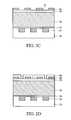
- FIGS. 1A to 1 Cdepict cross-sectional diagrams of the formation of a via hole between metal interconnects using conventional technique.
- a semiconductor substrate 10has a metal wire structure 12 , a low-k dielectric layer 14 formed over the exposed substrate 10 and the metal wire structure 12 , an oxide hard mask 16 deposited over the low-k dielectric layer 14 , and a photoresist layer 18 patterned on the oxide hard mask 16 .
- the oxide hard mask 16is etched to form an opening above the metal wire structure 12 .
- FIG. 1Betching is continued to form a via hole 19 in the low-k dielectric layer 14 .
- the via hole 19 with steep sidewalls 15exposes the metal wire structure 12 .
- the photoresist layer 18is removed by oxygen plasma process.
- the low-k dielectric layer 14 of carbon-containing organic polymerhas properties very similar to the photoresist layer 18 , and the low-k dielectric layer 14 , has very low resistance against oxygen plasma etching. Therefore, as shown in FIG. 1C, a portion of the exposed sidewalls 15 will be removed during the oxygen plasma process, resulting in recess cavities 15 a forming on the sidewalls 15 . Also, if a BARC is used under the photoresist layer 18 , the etch profile of the via hole 19 will be more difficult to control.
- SiO 2 based materialssuch as FSG, USG, black diamond, Coral, Aurora, and Flowfill are suitable for making the low-k dielectric layer 14 .
- the use of low-k organic materialsis limited in conventional technique.
- U.S. Pat. No. 6,159,661discloses a damascene process including the formation of an additional cap layer, preferably of silicon oxynitride (SiON), over the oxide hard mask.
- the cap layeris able to protect the low-k dielectric layer from oxygen plasma process when stripping the photoresist layer.
- the problem of tuning a high etching-selectivity between the cap layer and the oxide hard maskis encountered. Further, only low-k organic materials can be applied to the formation of the ILD layers.
- the present inventionis a dual damascene process with dual hard masks, in which at least the hard mask contact the low-k dielectric layer is of metallic materials.
- the dual damascene processis provided on a semiconductor substrate, which has a conductive structure, a dielectric separation layer covering the conductive structure, and a low-k dielectric layer over the dielectric separation layer.
- the conductive structureis preferably copper.
- the low-k dielectric layermay be of organic polymer formed by a spin-on coating process, and alternatively may be SiO2-based materials formed by chemical vapor deposition (CVD).
- a patterned etch stop layeris additionally provided in the low-k dielectric layer serving as a hard mask in the subsequent process of forming a via hole and serving as an etching endpoint in the subsequent process of forming a trench.
- a first hard mask of metallic materialis formed on the low-k dielectric layer, and then a second hard mask is formed on the first hard mask.
- the second hard maskmay be metallic or dielectric material.
- a first openingis formed in the second hard mask over the conductive structure, and then a second opening is formed in the first hard mask under the first opening. The diameter of the first opening is larger then the second opening.
- the low-k dielectric layer that is not covered by the first hard maskis removed until the dielectric separation layer is exposed, thereby forming a via hole in the low-k dielectric layer.
- the first hard mask that is not covered by the second hard maskis removed, and the exposed low-k dielectric layer is then removed to reach a predetermined depth.
- a trenchis formed over the via hole, and the trench and the via hole serve as a dual damascene opening.
- Yet another object of the inventionis to provide low-k organic materials in the formation of the low-k dielectric layer.
- Still another object of the inventionis to provide the dual hard masks as an anti-reflection coating (ARC) in subsequent deep ultra violet (DUV) photolithographic operations.
- ARCanti-reflection coating
- DUVdeep ultra violet
- Another object of the inventionis to lower the production cost and simplify the dual damascene process.
- FIGS. 1A to 1 Care cross-sectional diagrams showing a conventional technique of forming a via hole between metal interconnects.
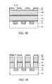
- FIGS. 2A to 2 Lare cross-sectional diagrams showing a dual damascene process in the first embodiment of the present invention.
- FIGS. 3A to 3 Iare cross-sectional diagrams showing a dual damascene process in the second embodiment of the present invention.
- FIGS. 4A to 4 Jare cross-sectional diagrams showing a dual damascene process in the third embodiment of the present invention.
- a dual damascene process using dual hard masksis provided.
- the dual hard masksare both of metallic material.
- one of the dual hard masks, positioned on the low-k dielectric layer,is of metallic material.
- FIGS. 2A to 2 Lare cross-sectional diagrams showing a dual damascene process in the first embodiment of the present invention.
- a semiconductor substrate 30comprises a plurality of metal wire structures 32 , a dielectric separation layer 34 covering the metal wire structures 32 and the exposed substrate 30 , and a low-k dielectric layer 36 formed on the dielectric separation layer 34 .
- the dielectric separation layer 34prevents the metal wire structures 32 from oxidizing and prevents the atoms/ions in the metal wire structures 32 from diffusing into the first insulating layer 36 .
- the metal wire structure 32is copper
- the dielectric separation layer 34is silicon nitride or silicon carbide.
- the low-k dielectric layer 36is of organic materials, such as spin-on polymer (SOP), FLARE, SILK, Parylene and/or PAE-II, and formed through a spin-coating process.
- the low-k dielectric layer 36is of SiO 2 -based materials, such as SiO 2 , FSG or USG, and formed through a spin-coating process, or black diamond, Coral, Aurora, and Flowfill, and formed through a chemical vapor deposition (CVD) process.
- first hard mask 38 and a second hard mask 40are sequentially formed on the low-k dielectric layer 36 .
- the first hard mask 38is of metallic material, such as Ti, TiN, Ta, TaN, Al, or AlCu.
- the second hard mask 40is preferably of metallic materials, such as Ti, TiN, Ta, TaN, Al, or AlCu, and alternatively of dielectric materials, such as SiO 2 , SiC, SiN, SRO or SiON.
- a first photoresist layer 42is patterned on the second hard mask 40 to define a trench of a dual damascene opening, and then a plurality of first openings 41 are formed in the second hard mask 40 with the first photoresist layer 42 as a mask.
- the first photoresist layer 42is removed.
- a second photoresist layer 44is patterned on the second hard mask 40 and the first hard mask 38 to define a via hole of a dual damascene opening, and then a plurality of second openings 43 are formed in the exposed first hard mask 38 with the second photoresist layer 44 as a mask.
- the second photoresist layer 44is removed. Note that the diameter of the first opening 41 is larger than the diameter of the second opening 43 .
- a plurality of via holes 45 over the metal wire structures 32are respectively formed in the low-k dielectric layer 36 with the dielectric separation layer 34 as an etch stop layer. Since the second photoresist layer 44 is removed prior to the formation of the via holes 45 , the exposed sidewalls of the low-k dielectric layer 36 are not vulnerable to damage by oxygen plasma.
- the exposed regions of the first hard mask 38are etched to level off the sidewalls of the dual hard masks 38 and 40 , and then the exposed low-k dielectric layer 36 is etched to reach a predetermined depth.
- a plurality of trenches 47 passing through the via holes 45are respectively formed in the low-k dielectric layer 36 .
- the trench 47 and the underlying via hole 45serve as a dual damascene opening 46 .
- the exposed dielectric separation layer 34 and the second hard mask 40are removed. As a result, the metal wire structure 32 is exposed at the bottom of the dual damascene opening 46 .
- a barrier layer 48is conformally deposited along the exposed surface of the semiconductor substrate 30 .
- the barrier layer 48is Ta/TaN, Ti/TiN or W/WN.
- One purpose of the barrier layer 48is to encapsulate copper interconnect from the surrounding low-k dielectric layer 36 , and the other purpose is to provide the adhesion between copper interconnect and the surrounding low-k dielectric layer 36 .
- a conductive layer 50preferably of copper, may be deposited by PVD, CVD, plating technique, or a combination of these techniques to fill the dual damascene openings 46 .
- the method of the conductive layer 56 's depositis a design choice dependent on the fabrication process being employed.
- the conductive layer 50 and the barrier layer 48 residing above the trench 47 levelare removed by either an etching or polishing technique.
- CMPchemical-mechanical polishing
- the conductive layer 50 and the barrier layer 48 residing above the trench 47 levelare removed by either an etching or polishing technique.
- CMPchemical-mechanical polishing
- the remaining part of the conductive layer 50serves as the dual damascene structure 50 ′.
- a sealing layer 52is deposited over the exposed surface of the semiconductor substrate 30 so as to cover the top of the dual damascene structure 50 ′.
- the sealing layer 52preferably of SiN or SiC, prevents the dual damascene structure 50 ′ from oxidizing and prevents the atoms/ions in the dual damascene structure 50 ′ from diffusing into the subsequently formed dielectric layer over the dual damascene structure 50 ′.
- additional interconnect structurescan be fabricated to form metallization levels above the dual damascene structure 50 ′.
- the dual damascene process of this inventionhas the following advantages: First, the dual hard masks 38 and 40 , preferably of metallic materials, are able to prevent oxygen plasma from contact with the low-k dielectric layer 36 when the photoresist layers 42 and 44 are removed. Hence, the gap-filling capacity of subsequently deposited conductive layer 50 in the dual damascene opening 46 can be increased. Second, since the damage to the low-k dielectric layer 36 from the oxygen plasma is avoided, the use of low-k organic materials may be applied to the formation of the low-k dielectric layer 36 . This can reduce RC delay and cross talk, and therefore chip size can be scaled down to the next generation.
- the dual hard masks 38 and 40can function as an anti-reflection coating (ARC) in subsequent deep ultra violet (DUV) photolithographic operations. Since a separate ARC is not necessary, production costs are lowered and the dual damascene process is simplified. Fourth, there is no need to form an etch stop layer inside the low-k dielectric layer 36 in the first embodiment, thus the formation of the low-k dielectric layer 36 is a one-stage operation, such as performing spin-on coating process or CVD process. This further lowers costs and simplifies the dual damascene process.
- ARCanti-reflection coating
- DUVdeep ultra violet
- a dual damascene process using one hard maskis provided.
- the hard maskis of metallic material.
- FIGS. 3A to 3 Iare cross-sectional diagrams showing a dual damascene process in the first embodiment of the present invention.
- the semiconductor substrate 30has metal wire structures 32 , the dielectric separation layer 34 , the low-k dielectric layer 36 formed on the dielectric separation layer 34 , and the hard mask 40 formed on the low-k dielectric layer 36 .
- the hard mask 40is of metallic material, such as Ti, TiN, Ta, TaN, Al, or AlCu.
- the first photoresist layer 42is patterned on the hard mask 40 to define a trench of a dual damascene opening, and then the first openings 41 are formed in the hard mask 40 with the first photoresist layer 42 as a mask. Next, the first photoresist layer 42 is removed. As shown in FIGS. 3D and 3E, the second photoresist layer 44 is patterned on the hard mask 40 and the low-k dielectric layer 36 to define a via hole of a dual damascene opening, and then the second openings 43 are formed in the second photoresist layer 44 .
- the via holes 45 over the metal wire structures 32are respectively formed in the low-k dielectric layer 36 .
- the depth of the via hole 45is larger than half of the height of the low-k dielectric layer 36 .
- the second photoresist layer 44is removed. Note that since the diameter of the first opening 41 is larger than the diameter of the second opening 43 , a part of the low-k dielectric layer 36 surrounding the via hole 45 is exposed.
- the low-k dielectric layer 36 underlying the via holes 45is etched to expose the dielectric separation layer 34 over the metal wire structures 32 .
- the low-k dielectric layer 36 surrounding the via hole 45is etched to reach a predetermined depth.
- the trenches 47 passing through the via holes 45are respectively formed in the low-k dielectric layer 36 .
- the trench 47 and the underlying via hole 45serve as a dual damascene opening 46 .
- the exposed dielectric separation layer 34 and the hard mask 40are removed.
- the metal wire structure 32is exposed at the bottom of the dual damascene opening 46 .
- a method of forming a dual damascene structure in the dual damascene opening 46is provided.
- the nature of the dual damascene structure's fabricationis a design choice dependent on the fabrication process being employed.
- the above-mentioned method shown in FIGS. 2J to 2 Lcan be provided to form a dual damascene structure in the dual damascene opening 46 .
- a dual damascene process using dual hard masksis provided wherein an etch stop layer is additionally provided in the low-dielectric layer.
- the dual hard masksare both of metallic materials.
- one of the dual hard masksis of metallic materials.
- FIGS. 4A to 4 Jare cross-sectional diagrams showing a dual damascene process in the second embodiment of the present invention.
- the semiconductor substrate 30comprises the metal wire structures 32 , the dielectric separation layer 34 covering the metal wire structures 32 and the exposed substrate 30 , a first low-k dielectric layer 361 formed on the dielectric separation layer 34 , an etching stop layer 35 formed on the first low-k dielectric layer 361 , and a second low-k dielectric layer 362 formed on the etch stop layer 35 .
- the materials of the first low-k dielectric layer 361 and the second low-k dielectric layer 362may be selected from organic materials, such as spin-on polymer (SOP), FLARE, SILK, Parylene and/or PAE-II, and formed through a spin-coating process.
- organic materialssuch as spin-on polymer (SOP), FLARE, SILK, Parylene and/or PAE-II
- the materials of the first low-k dielectric layer 361 and the second low-k dielectric layer 362may be selected from SiO 2 based materials, such as SiO 2 , FSG or USG through a spin-coating process, or black diamond, Coral, Aurora, and Flowfill, and formed through CVD process.
- the etching stop layer 35may be of SiO 2 , SiC, SiN, SRO or SiON, and serves as an etching endpoint of the trench 47 and as a hard mask of the via hole 45 .
- the first hard mask 38 and the second hard mask 40are sequentially formed on the second low-k dielectric layer 362 .
- the first hard mask 38may be of metallic materials selected from Ti, TiN, Ta, TaN, Al, or AlCu.
- the second hard mask 40may be of metallic materials selected from Ti, TiN, Ta, TaN, Al, or AlCu, and alternatively may be of dielectric materials selected from SiO 2 , SiC, SiN, SRO or SiON.
- the processes used in the fabrication of the first photoresist layer 42 , the first openings 41 , the second photoresist layer 44 , and the second openings 43are substantially the same as the processes used in the first embodiment.
- the via holes 45are formed over the metal wire structures 32 respectively.
- the exposed regions of the first hard mask 38are etched to level off the sidewalls of the dual hard masks 38 and 40 , and then the exposed second low-k dielectric layer 362 is etched until the etch stop layer 35 is exposed.
- the trenches 47 corresponding to the via holes 45are formed in the second low-k dielectric layer 362 .
- the trench 47 and the underlying via hole 45serve as the dual damascene opening 46 .
- the exposed dielectric separation layer 34 and the second hard mask 40are removed. As a result, the metal wire 12 is exposed at the bottom of the dual damascene opening 46 .
- a dual damascene structureis provided in the dual damascene opening 46 .
- the nature of the dual damascene structure's fabricationis a design choice dependent on the fabrication process being employed.
- the processes used in the fabrication of the barrier layer 48 , the conductive layer 50 , the damascene structure 50 ′, and the sealing layer 52are substantially the same as the processes used in the first embodiment.
Landscapes
- Engineering & Computer Science (AREA)
- Physics & Mathematics (AREA)
- Condensed Matter Physics & Semiconductors (AREA)
- General Physics & Mathematics (AREA)
- Manufacturing & Machinery (AREA)
- Computer Hardware Design (AREA)
- Microelectronics & Electronic Packaging (AREA)
- Power Engineering (AREA)
- Internal Circuitry In Semiconductor Integrated Circuit Devices (AREA)
Abstract


Description
- 1. Field of the Invention[0001]
- The present invention relates to a dual damascene process and, more particularly, to a dual damascene process using at least one metal hard mask.[0002]
- 2. Description of the Related Art[0003]
- High-density integrated circuits, such as very large scale integration (VLSI) circuits, are typically formed with multiple metal interconnects to serve as three-dimensional wiring line structures. The purpose of multiple interconnects is to properly link the densely packed devices together. With increasing levels of integration, a parasitic capacitance effect between the metal interconnects, which leads to RC delay and cross talk, increases correspondingly. Therefore, in order to reduce the parasitic capacitance for increasing the speed of conduction between the metal interconnections, a type of low-k organic dielectric material is commonly employed to form an inter-layer dielectric (ILD) layer. However, there are technical problems regarding the use of low-k organic dielectric materials for the ILD layers.[0004]
- FIGS. 1A to[0005]1C depict cross-sectional diagrams of the formation of a via hole between metal interconnects using conventional technique. As shown in FIG. 1A, a
semiconductor substrate 10 has ametal wire structure 12, a low-kdielectric layer 14 formed over the exposedsubstrate 10 and themetal wire structure 12, an oxidehard mask 16 deposited over the low-kdielectric layer 14, and aphotoresist layer 18 patterned on the oxidehard mask 16. Using thephotoresist layer 18 as a mask, the oxidehard mask 16 is etched to form an opening above themetal wire structure 12. Then, as shown in FIG. 1B, etching is continued to form avia hole 19 in the low-kdielectric layer 14. Thevia hole 19 withsteep sidewalls 15 exposes themetal wire structure 12. Finally, thephotoresist layer 18 is removed by oxygen plasma process. However, the low-kdielectric layer 14 of carbon-containing organic polymer has properties very similar to thephotoresist layer 18, and the low-kdielectric layer 14, has very low resistance against oxygen plasma etching. Therefore, as shown in FIG. 1C, a portion of the exposedsidewalls 15 will be removed during the oxygen plasma process, resulting inrecess cavities 15aforming on thesidewalls 15. Also, if a BARC is used under thephotoresist layer 18, the etch profile of thevia hole 19 will be more difficult to control. In addition, since the oxygen plasma easily poisons low-k organic materials, only SiO2based materials such as FSG, USG, black diamond, Coral, Aurora, and Flowfill are suitable for making the low-kdielectric layer 14. Thus, the use of low-k organic materials is limited in conventional technique. - Seeking to solve the aforementioned problems, U.S. Pat. No. 6,159,661 discloses a damascene process including the formation of an additional cap layer, preferably of silicon oxynitride (SiON), over the oxide hard mask. The cap layer is able to protect the low-k dielectric layer from oxygen plasma process when stripping the photoresist layer. However, when patterning the cap layer, the problem of tuning a high etching-selectivity between the cap layer and the oxide hard mask is encountered. Further, only low-k organic materials can be applied to the formation of the ILD layers.[0006]
- Thus, a dual damascene process using dual hard masks, in which at least the hard mask contacting the low-k dielectric layer is of metallic materials, is desired to solve the aforementioned problems[0007]
- The present invention is a dual damascene process with dual hard masks, in which at least the hard mask contact the low-k dielectric layer is of metallic materials.[0008]
- The dual damascene process is provided on a semiconductor substrate, which has a conductive structure, a dielectric separation layer covering the conductive structure, and a low-k dielectric layer over the dielectric separation layer. The conductive structure is preferably copper. The low-k dielectric layer may be of organic polymer formed by a spin-on coating process, and alternatively may be SiO2-based materials formed by chemical vapor deposition (CVD). In another preferred embodiment, a patterned etch stop layer is additionally provided in the low-k dielectric layer serving as a hard mask in the subsequent process of forming a via hole and serving as an etching endpoint in the subsequent process of forming a trench.[0009]
- A first hard mask of metallic material is formed on the low-k dielectric layer, and then a second hard mask is formed on the first hard mask. The second hard mask may be metallic or dielectric material. Next, using photolithography and etching, a first opening is formed in the second hard mask over the conductive structure, and then a second opening is formed in the first hard mask under the first opening. The diameter of the first opening is larger then the second opening. Afterward, the low-k dielectric layer that is not covered by the first hard mask is removed until the dielectric separation layer is exposed, thereby forming a via hole in the low-k dielectric layer. Thereafter, the first hard mask that is not covered by the second hard mask is removed, and the exposed low-k dielectric layer is then removed to reach a predetermined depth. As a result, a trench is formed over the via hole, and the trench and the via hole serve as a dual damascene opening.[0010]
- Accordingly, it is a principle object of the invention to provide dual metal hard masks for preventing oxygen plasma from making contact the low-k dielectric layer when a photoresist layer is removed.[0011]
- It is another object of the invention to increase the gap-filling capacity of the subsequently deposited conductive layer in the dual damascene opening.[0012]
- Yet another object of the invention is to provide low-k organic materials in the formation of the low-k dielectric layer.[0013]
- It is a further object of the invention to reduce RC delay and cross talk, therefore allowing chip size to be scaled down to the next generation.[0014]
- Still another object of the invention is to provide the dual hard masks as an anti-reflection coating (ARC) in subsequent deep ultra violet (DUV) photolithographic operations.[0015]
- Another object of the invention is to lower the production cost and simplify the dual damascene process.[0016]
- These and other objects of the present invention will become readily apparent upon further review of the following specification and drawings.[0017]
- FIGS. 1A to[0018]1C are cross-sectional diagrams showing a conventional technique of forming a via hole between metal interconnects.
- FIGS. 2A to[0019]2L are cross-sectional diagrams showing a dual damascene process in the first embodiment of the present invention.
- FIGS. 3A to[0020]3I are cross-sectional diagrams showing a dual damascene process in the second embodiment of the present invention.
- FIGS. 4A to[0021]4J are cross-sectional diagrams showing a dual damascene process in the third embodiment of the present invention.
- Similar reference characters denote corresponding features consistently throughout the attached drawings.[0022]
- [First Embodiment][0023]
- A dual damascene process using dual hard masks is provided. Preferably, the dual hard masks are both of metallic material. Alternatively, one of the dual hard masks, positioned on the low-k dielectric layer, is of metallic material.[0024]
- FIGS. 2A to[0025]2L are cross-sectional diagrams showing a dual damascene process in the first embodiment of the present invention. As shown in FIG. 2A, a
semiconductor substrate 30 comprises a plurality ofmetal wire structures 32, adielectric separation layer 34 covering themetal wire structures 32 and the exposedsubstrate 30, and a low-k dielectric layer 36 formed on thedielectric separation layer 34. Thedielectric separation layer 34 prevents themetal wire structures 32 from oxidizing and prevents the atoms/ions in themetal wire structures 32 from diffusing into the first insulatinglayer 36. Preferably, themetal wire structure 32 is copper, and thedielectric separation layer 34 is silicon nitride or silicon carbide. The low-k dielectric layer 36 is of organic materials, such as spin-on polymer (SOP), FLARE, SILK, Parylene and/or PAE-II, and formed through a spin-coating process. Alternatively, the low-k dielectric layer 36 is of SiO2-based materials, such as SiO2, FSG or USG, and formed through a spin-coating process, or black diamond, Coral, Aurora, and Flowfill, and formed through a chemical vapor deposition (CVD) process. - In addition, a first[0026]
hard mask 38 and a secondhard mask 40 are sequentially formed on the low-k dielectric layer 36. Preferably, the firsthard mask 38 is of metallic material, such as Ti, TiN, Ta, TaN, Al, or AlCu. The secondhard mask 40 is preferably of metallic materials, such as Ti, TiN, Ta, TaN, Al, or AlCu, and alternatively of dielectric materials, such as SiO2, SiC, SiN, SRO or SiON. - As shown in FIGS. 2B and 2C, a[0027]
first photoresist layer 42 is patterned on the secondhard mask 40 to define a trench of a dual damascene opening, and then a plurality offirst openings 41 are formed in the secondhard mask 40 with thefirst photoresist layer 42 as a mask. Next, thefirst photoresist layer 42 is removed. As shown in FIGS. 2D and 2E, asecond photoresist layer 44 is patterned on the secondhard mask 40 and the firsthard mask 38 to define a via hole of a dual damascene opening, and then a plurality ofsecond openings 43 are formed in the exposed firsthard mask 38 with thesecond photoresist layer 44 as a mask. Next, thesecond photoresist layer 44 is removed. Note that the diameter of thefirst opening 41 is larger than the diameter of thesecond opening 43. - As shown in FIG. 2F, using a dry etching process with the first[0028]
hard mask 38, a plurality of viaholes 45 over themetal wire structures 32 are respectively formed in the low-k dielectric layer 36 with thedielectric separation layer 34 as an etch stop layer. Since thesecond photoresist layer 44 is removed prior to the formation of the via holes45, the exposed sidewalls of the low-k dielectric layer 36 are not vulnerable to damage by oxygen plasma. - As shown in FIGS. 2G and 2H, the exposed regions of the first[0029]
hard mask 38 are etched to level off the sidewalls of the dualhard masks k dielectric layer 36 is etched to reach a predetermined depth. Thus, a plurality oftrenches 47 passing through the via holes45 are respectively formed in the low-k dielectric layer 36. Thetrench 47 and the underlying viahole 45 serve as adual damascene opening 46. As shown in FIG. 2I, the exposeddielectric separation layer 34 and the secondhard mask 40 are removed. As a result, themetal wire structure 32 is exposed at the bottom of thedual damascene opening 46. - Hereinafter, a method of forming a dual damascene structure in the[0030]
dual damascene opening 46 is provided. Naturally, the nature of the dual damascene structure's fabrication is a design choice dependent on the fabrication process being employed. - As shown in FIG. 2J, a[0031]
barrier layer 48 is conformally deposited along the exposed surface of thesemiconductor substrate 30. Preferably, thebarrier layer 48 is Ta/TaN, Ti/TiN or W/WN. One purpose of thebarrier layer 48 is to encapsulate copper interconnect from the surrounding low-k dielectric layer 36, and the other purpose is to provide the adhesion between copper interconnect and the surrounding low-k dielectric layer 36. Then, aconductive layer 50, preferably of copper, may be deposited by PVD, CVD, plating technique, or a combination of these techniques to fill thedual damascene openings 46. The method of the conductive layer56's deposit is a design choice dependent on the fabrication process being employed. - As shown in FIG. 2K, the[0032]
conductive layer 50 and thebarrier layer 48 residing above thetrench 47 level are removed by either an etching or polishing technique. In the preferred embodiment, chemical-mechanical polishing (CMP) is used to polish away the excessconductive layer 50 and thebarrier layer 48 so as to level off the top surface of theconductive layer 50 and the firsthard mask 38. Consequently, the remaining part of theconductive layer 50 serves as thedual damascene structure 50′. - Finally, as shown in FIG. 2L, a[0033]
sealing layer 52 is deposited over the exposed surface of thesemiconductor substrate 30 so as to cover the top of thedual damascene structure 50′. Thesealing layer 52, preferably of SiN or SiC, prevents thedual damascene structure 50′ from oxidizing and prevents the atoms/ions in thedual damascene structure 50′ from diffusing into the subsequently formed dielectric layer over thedual damascene structure 50′. In addition, by repeating the processes, additional interconnect structures can be fabricated to form metallization levels above thedual damascene structure 50′. - The dual damascene process of this invention has the following advantages: First, the dual[0034]
hard masks k dielectric layer 36 when the photoresist layers42 and44 are removed. Hence, the gap-filling capacity of subsequently depositedconductive layer 50 in thedual damascene opening 46 can be increased. Second, since the damage to the low-k dielectric layer 36 from the oxygen plasma is avoided, the use of low-k organic materials may be applied to the formation of the low-k dielectric layer 36. This can reduce RC delay and cross talk, and therefore chip size can be scaled down to the next generation. Third, the dualhard masks k dielectric layer 36 in the first embodiment, thus the formation of the low-k dielectric layer 36 is a one-stage operation, such as performing spin-on coating process or CVD process. This further lowers costs and simplifies the dual damascene process. - [Second Embodiment][0035]
- A dual damascene process using one hard mask is provided. Preferably, the hard mask is of metallic material.[0036]
- FIGS. 3A to[0037]3I are cross-sectional diagrams showing a dual damascene process in the first embodiment of the present invention. As shown in FIG. 3A, the
semiconductor substrate 30 hasmetal wire structures 32, thedielectric separation layer 34, the low-k dielectric layer 36 formed on thedielectric separation layer 34, and thehard mask 40 formed on the low-k dielectric layer 36. Preferably, thehard mask 40 is of metallic material, such as Ti, TiN, Ta, TaN, Al, or AlCu. - As shown in FIGS. 3B and 3C, the[0038]
first photoresist layer 42 is patterned on thehard mask 40 to define a trench of a dual damascene opening, and then thefirst openings 41 are formed in thehard mask 40 with thefirst photoresist layer 42 as a mask. Next, thefirst photoresist layer 42 is removed. As shown in FIGS. 3D and 3E, thesecond photoresist layer 44 is patterned on thehard mask 40 and the low-k dielectric layer 36 to define a via hole of a dual damascene opening, and then thesecond openings 43 are formed in thesecond photoresist layer 44. - As shown in FIG. 3F, using a dry etching process with the[0039]
second photoresist layer 44, the via holes45 over themetal wire structures 32 are respectively formed in the low-k dielectric layer 36. Preferably, the depth of the viahole 45 is larger than half of the height of the low-k dielectric layer 36. Next, as shown in FIG. 3G, thesecond photoresist layer 44 is removed. Note that since the diameter of thefirst opening 41 is larger than the diameter of thesecond opening 43, a part of the low-k dielectric layer 36 surrounding the viahole 45 is exposed. - As shown in FIG. 3H, using dry etching with the[0040]
hard mask 40, the low-k dielectric layer 36 underlying the via holes45 is etched to expose thedielectric separation layer 34 over themetal wire structures 32. Meanwhile, the low-k dielectric layer 36 surrounding the viahole 45 is etched to reach a predetermined depth. Thus, thetrenches 47 passing through the via holes45 are respectively formed in the low-k dielectric layer 36. Thetrench 47 and the underlying viahole 45 serve as adual damascene opening 46. As shown in FIG. 3I, the exposeddielectric separation layer 34 and thehard mask 40 are removed. As a result, themetal wire structure 32 is exposed at the bottom of thedual damascene opening 46. - Hereinafter, a method of forming a dual damascene structure in the[0041]
dual damascene opening 46 is provided. Naturally, the nature of the dual damascene structure's fabrication is a design choice dependent on the fabrication process being employed. The above-mentioned method shown in FIGS. 2J to2L can be provided to form a dual damascene structure in thedual damascene opening 46. - [Third Embodiment][0042]
- A dual damascene process using dual hard masks is provided wherein an etch stop layer is additionally provided in the low-dielectric layer. Preferably, the dual hard masks are both of metallic materials. Alternatively, one of the dual hard masks is of metallic materials.[0043]
- FIGS. 4A to[0044]4J are cross-sectional diagrams showing a dual damascene process in the second embodiment of the present invention. As shown in FIG. 4A, the
semiconductor substrate 30 comprises themetal wire structures 32, thedielectric separation layer 34 covering themetal wire structures 32 and the exposedsubstrate 30, a first low-k dielectric layer 361 formed on thedielectric separation layer 34, anetching stop layer 35 formed on the first low-k dielectric layer 361, and a second low-k dielectric layer 362 formed on theetch stop layer 35. The materials of the first low-k dielectric layer 361 and the second low-k dielectric layer 362 may be selected from organic materials, such as spin-on polymer (SOP), FLARE, SILK, Parylene and/or PAE-II, and formed through a spin-coating process. Alternatively, the materials of the first low-k dielectric layer 361 and the second low-k dielectric layer 362 may be selected from SiO2based materials, such as SiO2, FSG or USG through a spin-coating process, or black diamond, Coral, Aurora, and Flowfill, and formed through CVD process. - The[0045]
etching stop layer 35, may be of SiO2, SiC, SiN, SRO or SiON, and serves as an etching endpoint of thetrench 47 and as a hard mask of the viahole 45. In addition, the firsthard mask 38 and the secondhard mask 40 are sequentially formed on the second low-k dielectric layer 362. Preferably, the firsthard mask 38 may be of metallic materials selected from Ti, TiN, Ta, TaN, Al, or AlCu. The secondhard mask 40 may be of metallic materials selected from Ti, TiN, Ta, TaN, Al, or AlCu, and alternatively may be of dielectric materials selected from SiO2, SiC, SiN, SRO or SiON. - As shown in FIGS. 4B to[0046]4E, the processes used in the fabrication of the
first photoresist layer 42, thefirst openings 41, thesecond photoresist layer 44, and thesecond openings 43 are substantially the same as the processes used in the first embodiment. - As shown in FIG. 4F, using a dry etching process with the first[0047]
hard mask 38, the second low-k dielectric layer 362, theetch stop layer 35 and the first low-k dielectric layer 361 under thesecond openings 43 are removed with thedielectric separation layer 34 as an etch stop layer. Thus, the via holes45 are formed over themetal wire structures 32 respectively. - As shown in FIGS. 4G and 4H, the exposed regions of the first[0048]
hard mask 38 are etched to level off the sidewalls of the dualhard masks k dielectric layer 362 is etched until theetch stop layer 35 is exposed. Thus, thetrenches 47 corresponding to the via holes45 are formed in the second low-k dielectric layer 362. Thetrench 47 and the underlying viahole 45 serve as thedual damascene opening 46. As shown in FIG. 4I, the exposeddielectric separation layer 34 and the secondhard mask 40 are removed. As a result, themetal wire 12 is exposed at the bottom of thedual damascene opening 46. - Hereinafter, a dual damascene structure is provided in the[0049]
dual damascene opening 46. Naturally, the nature of the dual damascene structure's fabrication is a design choice dependent on the fabrication process being employed. Preferably, as shown in FIG. 4J, the processes used in the fabrication of thebarrier layer 48, theconductive layer 50, thedamascene structure 50′, and thesealing layer 52 are substantially the same as the processes used in the first embodiment. - It is to be understood that the present invention is not limited to the embodiments described above, but encompasses any and all embodiments within the scope of the following claims.[0050]
Claims (27)
1. A dual damascene process, comprising the steps of:
providing a semiconductor substrate which has a conductive structure, a dielectric separation layer covering the conductive structure and a low-k dielectric layer over the dielectric separation layer;
forming a first hard mask of metallic materials on the low-k dielectric layer;
forming a second hard mask on the first hard mask;
forming a first opening in the second hard mask over the conductive structure;
forming a second opening in the first hard mask under the first opening, wherein the diameter of the first opening is larger then the second opening;
removing the low-k dielectric layer not covered by the first hard mask until the dielectric separation layer is exposed so as to form a via hole;
removing the first hard mask not covered by the second hard mask; and
removing the low-k dielectric layer not covered by the first hard mask to reach a predetermined depth so as to form a trench over the via hole, wherein the trench and the via hole serve as a dual damascene opening.
2. The dual damascene process according toclaim 1 , wherein the first hard mask is of metallic materials selected from Ti, TiN, Ta, TaN, Al, or AlCu.
3. The dual damascene process according toclaim 1 , wherein the second hard mask is of metallic material selected from Ti, TiN, Ta, TaN, Al, or AlCu.
4. The dual damascene process according toclaim 1 , wherein the second hard mask is of dielectric materials selected from SiO2, SiC, SiN, SRO or SiON.
5. The dual damascene process according toclaim 1 , wherein the low-k dielectric layer is of organic polymer formed by a spin-on coating process.
6. The dual damascene process according toclaim 1 , wherein the low-k dielectric layer is of SiO2based materials formed by a chemical vapor deposition (CVD) process.
7. The dual damascene process according toclaim 1 , further comprising a step of removing the exposed dielectric separation layer at the bottom of the dual damascene opening to expose the conductive structure.
8. The dual damascene process according toclaim 7 , further comprising a step of forming a conductive layer to fill the dual damascene opening.
9. The dual damascene process according toclaim 8 , further comprising a step of forming a barrier layer on the sidewall and bottom of the dual damascene opening prior to the formation of the conductive layer.
10. A dual damascene process, comprising the steps of:
providing a semiconductor substrate which has a conductive structure, a dielectric separation layer covering the conductive structure and a low-k dielectric layer over the dielectric separation layer;
forming a hard mask of metallic materials on the low-k dielectric layer;
forming a first opening in the hard mask over the conductive structure;
forming a photoresist layer on the hard mask to cover part of the first opening, wherein the photoresist layer has a second opening and the diameter of the first opening is larger then the second opening;
removing the low-k dielectric layer not covered by the photoresist layer to reach a predetermined depth so as to form a via hole;
removing the photoresist layer; and
removing the low-k dielectric layer underlying the via hole to expose the dielectric separation layer, and removing the low-k dielectric layer surrounding the via hole to reach the predetermined depth so as to form a trench over the via hole, wherein the trench and the via hole serve as a dual damascene opening.
11. The dual damascene process according toclaim 10 , wherein the hard mask is of metallic materials selected from Ti, TiN, Ta, TaN, Al, or AlCu.
12. The dual damascene process according toclaim 10 , wherein the low-k dielectric layer is of organic polymer formed by a spin-on coating process.
13. The dual damascene process according toclaim 10 , wherein the low-k dielectric layer is of SiO2based materials formed by a chemical vapor deposition (CVD) process.
14. The dual damascene process according toclaim 10 , further comprising a step of removing the exposed dielectric separation layer at the bottom of the dual damascene opening to expose the conductive structure.
15. The dual damascene process according toclaim 14 , further comprising a step of forming a conductive layer to fill the dual damascene opening.
16. The dual damascene process according toclaim 15 , further comprising a step of forming a barrier layer on the sidewall and bottom of the dual damascene opening prior to the formation of the conductive layer.
17. A dual damascene process, comprising the steps of:
providing a semiconductor substrate which has a conductive structure and a dielectric separation layer covering the conductive structure;
forming a first low-k dielectric layer on the dielectric separation layer;
forming an etch stop layer on the first low-k dielectric layer, wherein the etch stop layer has an opening over the conductive structure;
forming a second low-k dielectric layer on the etch stop layer to fill the opening of the etch stop layer;
forming a first hard mask of metallic materials on the second low-k dielectric layer;
forming a second hard mask on the first hard mask;
forming a first opening in the second hard mask over the conductive structure;
forming a second opening in the first hard mask under the first opening, wherein the diameter of the first opening is larger then the second opening;
removing the second low-k dielectric layer not covered by the first hard mask and removing the first low-k dielectric layer not covered by the etch stop layer until the dielectric separation layer is exposed so as to form a via hole;
removing the first hard mask not covered by the second hard mask; and
removing the second low-k dielectric layer not covered by the first hard mask to reach a predetermined depth so as to form a trench over the via hole, wherein the trench and the via hole serves as a dual damascene opening.
18. The dual damascene process according toclaim 17 , wherein the first hard mask is of metallic materials selected from Ti, TiN, Ta, TaN, Al, or AlCu.
19. The dual damascene process according toclaim 17 , wherein the second hard mask is of metallic materials selected from Ti, TiN, Ta, TaN, Al, or AlCu.
20. The dual damascene process according toclaim 17 , wherein the second hard mask is of dielectric materials selected from SiO2, SiC, SiN, SRO or SiON.
21. The dual damascene process according toclaim 17 , wherein the first low-k dielectric layer is of organic polymer formed by a spin-on coating process.
22. The dual damascene process according toclaim 17 , wherein the first low-k dielectric layer is of SiO2based materials formed by a chemical vapor deposition (CVD) process.
23. The dual damascene process according toclaim 17 , wherein the second low-k dielectric layer is of organic polymer formed by a spin-on coating process.
24. The dual damascene process according toclaim 17 , wherein the second low-k dielectric layer is of SiO2based materials formed by a chemical vapor deposition (CVD) process.
25. The dual damascene process according toclaim 17 , further comprising a step of removing the exposed dielectric separation layer at the bottom of the dual damascene opening to expose the conductive structure.
26. The dual damascene process according toclaim 17 , further comprising a step of forming a conductive layer to fill the dual damascene opening.
27. The dual damascene process according toclaim 26 , further comprising a step of forming a barrier layer on the sidewall and bottom of the dual damascene opening prior to the formation of the conductive layer.
Priority Applications (1)
| Application Number | Priority Date | Filing Date | Title |
|---|---|---|---|
| US09/910,876US6696222B2 (en) | 2001-07-24 | 2001-07-24 | Dual damascene process using metal hard mask |
Applications Claiming Priority (1)
| Application Number | Priority Date | Filing Date | Title |
|---|---|---|---|
| US09/910,876US6696222B2 (en) | 2001-07-24 | 2001-07-24 | Dual damascene process using metal hard mask |
Publications (2)
| Publication Number | Publication Date |
|---|---|
| US20030044725A1true US20030044725A1 (en) | 2003-03-06 |
| US6696222B2 US6696222B2 (en) | 2004-02-24 |
Family
ID=25429439
Family Applications (1)
| Application Number | Title | Priority Date | Filing Date |
|---|---|---|---|
| US09/910,876Expired - LifetimeUS6696222B2 (en) | 2001-07-24 | 2001-07-24 | Dual damascene process using metal hard mask |
Country Status (1)
| Country | Link |
|---|---|
| US (1) | US6696222B2 (en) |
Cited By (43)
| Publication number | Priority date | Publication date | Assignee | Title |
|---|---|---|---|---|
| US20030199169A1 (en)* | 2002-04-17 | 2003-10-23 | Samsung Electronics Co., Ltd. | Method of forming dual damascene interconnection using low-k dielectric |
| US6638871B2 (en)* | 2002-01-10 | 2003-10-28 | United Microlectronics Corp. | Method for forming openings in low dielectric constant material layer |
| US6696222B2 (en)* | 2001-07-24 | 2004-02-24 | Silicon Integrated Systems Corp. | Dual damascene process using metal hard mask |
| US20040219796A1 (en)* | 2003-05-01 | 2004-11-04 | Chih-Ning Wu | Plasma etching process |
| US20040251234A1 (en)* | 2003-06-13 | 2004-12-16 | Kaushik Kumar | Bilayered metal hardmasks for use in dual damascene etch schemes |
| US20050070105A1 (en)* | 2003-03-14 | 2005-03-31 | Lam Research Corporation | Small volume process chamber with hot inner surfaces |
| US20050077628A1 (en)* | 2003-10-14 | 2005-04-14 | Kaushik Kumar | Dual damascene structure and method |
| US20050079706A1 (en)* | 2003-10-14 | 2005-04-14 | Kaushik Kumar | Dual damascene structure and method |
| WO2005038892A1 (en)* | 2003-10-08 | 2005-04-28 | Lam Research Corporation | A nitrous oxide stripping process for organosilicate glass |
| US20050090093A1 (en)* | 2003-03-14 | 2005-04-28 | Lam Research Corporation | Stress free etch processing in combination with a dynamic liquid meniscus |
| US20050087759A1 (en)* | 2003-03-14 | 2005-04-28 | Lam Research Corporation | System and method for surface reduction, passivation, corrosion prevention and activation of copper surface |
| US20050106848A1 (en)* | 2003-03-14 | 2005-05-19 | Lam Research Corporation | System and method for stress free conductor removal |
| US20050184394A1 (en)* | 2004-02-24 | 2005-08-25 | Sang-Woo Lee | Methods of forming a metal wiring in semiconductor devices using etch stop layers and devices so formed |
| US7022600B2 (en) | 2002-05-28 | 2006-04-04 | Samsung Electronics, Co., Ltd. | Method of forming dual damascene interconnection using low-k dielectric material |
| US20060134905A1 (en)* | 2004-11-23 | 2006-06-22 | Tymon Barwicz | Multilevel fabrication processing by functional regrouping of material deposition, lithography, and etching |
| US20060134921A1 (en)* | 2003-05-01 | 2006-06-22 | Chih-Ning Wu | Plasma etching process |
| US20060148243A1 (en)* | 2004-12-30 | 2006-07-06 | Jeng-Ho Wang | Method for fabricating a dual damascene and polymer removal |
| US20060240673A1 (en)* | 2005-04-22 | 2006-10-26 | Hynix Semiconductor | Method of forming bit line in semiconductor device |
| US20060286793A1 (en)* | 2005-06-15 | 2006-12-21 | Chin-Hsiang Lin | Stacked structure for forming damascene structure, method of fabricating the stacked structure, and damascene process |
| US20070054486A1 (en)* | 2005-09-05 | 2007-03-08 | Ta-Hung Yang | Method for forming opening |
| US20070105247A1 (en)* | 2002-01-30 | 2007-05-10 | Advanced Micro Devices | Method And Apparatus For Detecting The Endpoint Of A Chemical-Mechanical Polishing Operation |
| WO2008007259A2 (en) | 2006-06-21 | 2008-01-17 | Nxp B.V. | Semiconductor device and method of manufacturing a semiconductor device |
| US20080146036A1 (en)* | 2006-12-18 | 2008-06-19 | Yu-Tsung Lai | Semiconductor manufacturing process |
| WO2009047588A1 (en)* | 2007-10-09 | 2009-04-16 | Freescale Semiconductor, Inc. | Method for manufacturing a semiconductor device and semiconductor device obtainable with such a method |
| CN101572252B (en)* | 2008-04-28 | 2011-01-12 | 中芯国际集成电路制造(北京)有限公司 | Etching stopping layer, semiconductor device with through hole and method for forming same two |
| US20120270389A1 (en)* | 2011-04-20 | 2012-10-25 | United Microelectronics Corp. | Method for manufacturing interconnection structure and of metal nitride layer thereof |
| US20120309196A1 (en)* | 2011-06-01 | 2012-12-06 | Shougang Mi | Manufacturing method for dual damascene structure |
| CN102856248A (en)* | 2011-07-01 | 2013-01-02 | 中芯国际集成电路制造(上海)有限公司 | Method for forming double mosaic structure |
| US20130178057A1 (en)* | 2012-01-11 | 2013-07-11 | Globalfoundries Inc. | Methods of Forming Conductive Structures Using a Dual Metal Hard Mask Technique |
| CN103676491A (en)* | 2012-09-20 | 2014-03-26 | 中国科学院微电子研究所 | Method for reducing roughness of photoresist in electron beam lithography |
| US8828878B2 (en) | 2011-06-01 | 2014-09-09 | United Microelectronics Corp. | Manufacturing method for dual damascene structure |
| US20140273496A1 (en)* | 2013-03-14 | 2014-09-18 | Chia-Ling Kao | Method of removing a metal hardmask |
| CN104347488A (en)* | 2013-08-07 | 2015-02-11 | 中芯国际集成电路制造(上海)有限公司 | Forming method of interconnection structure |
| US20150104938A1 (en)* | 2013-10-16 | 2015-04-16 | United Microelectronics Corporation | Method for forming damascene opening and applications thereof |
| CN104701143A (en)* | 2013-12-10 | 2015-06-10 | 台湾积体电路制造股份有限公司 | Bi-layer hard mask for robust metallization profile |
| US9269563B2 (en)* | 2014-06-06 | 2016-02-23 | Applied Materials, Inc. | Methods for forming interconnect structure utilizing selective protection process for hardmask removal process |
| US9659811B1 (en)* | 2016-07-07 | 2017-05-23 | Taiwan Semiconductor Manufacturing Co., Ltd. | Manufacturing method of semiconductor device |
| WO2018004699A1 (en)* | 2016-07-01 | 2018-01-04 | Intel Corporation | Lined photobucket structure for back end of line (beol) interconnect formation |
| KR20180114490A (en)* | 2017-04-10 | 2018-10-18 | 타이완 세미콘덕터 매뉴팩쳐링 컴퍼니 리미티드 | Method for manufacturing a semiconductor device |
| CN109712932A (en)* | 2018-11-13 | 2019-05-03 | 友达光电股份有限公司 | Bendable array substrate and its manufacturing method |
| US20190139895A1 (en)* | 2017-11-08 | 2019-05-09 | Taiwan Semiconductor Manufacturing Co., Ltd. | Method for forming semiconductor device structure with conductive line |
| US11289375B2 (en) | 2020-03-23 | 2022-03-29 | International Business Machines Corporation | Fully aligned interconnects with selective area deposition |
| US20220392765A1 (en)* | 2021-06-04 | 2022-12-08 | Tokyo Electron Limited | Cyclic plasma processing |
Families Citing this family (44)
| Publication number | Priority date | Publication date | Assignee | Title |
|---|---|---|---|---|
| DE10127888A1 (en)* | 2001-06-08 | 2002-12-19 | Infineon Technologies Ag | Process for forming contact holes in contact regions of components integrated in a substrate comprises applying an insulating layer on a substrate with the integrated components, and applying a mask with openings |
| JP2003037162A (en)* | 2001-07-23 | 2003-02-07 | Tokyo Electron Ltd | Method of manufacturing semiconductor device |
| US20030213617A1 (en)* | 2002-05-20 | 2003-11-20 | Subramanian Karthikeyan | Method and structure of a reducing intra-level and inter-level capacitance of a semiconductor device |
| US20030064582A1 (en)* | 2001-09-28 | 2003-04-03 | Oladeji Isaiah O. | Mask layer and interconnect structure for dual damascene semiconductor manufacturing |
| US7186640B2 (en)* | 2002-06-20 | 2007-03-06 | Chartered Semiconductor Manufacturing Ltd. | Silicon-rich oxide for copper damascene interconnect incorporating low dielectric constant dielectrics |
| US20030234815A1 (en)* | 2002-06-21 | 2003-12-25 | Delaney Paul J. | Controlling a user interface |
| US6995073B2 (en)* | 2003-07-16 | 2006-02-07 | Intel Corporation | Air gap integration |
| US20050029221A1 (en)* | 2003-08-09 | 2005-02-10 | Taiwan Semiconductor Manufacturing Co., Ltd. | Deep trench etching using HDP chamber |
| US7915085B2 (en)* | 2003-09-18 | 2011-03-29 | Cree, Inc. | Molded chip fabrication method |
| US20050064629A1 (en)* | 2003-09-22 | 2005-03-24 | Chen-Hua Yu | Tungsten-copper interconnect and method for fabricating the same |
| US7015133B2 (en)* | 2004-04-14 | 2006-03-21 | Taiwan Semiconductor Manufacturing Company | Dual damascene structure formed of low-k dielectric materials |
| JP2006024811A (en)* | 2004-07-09 | 2006-01-26 | Sony Corp | Method for manufacturing semiconductor device |
| US7335588B2 (en)* | 2005-04-15 | 2008-02-26 | International Business Machines Corporation | Interconnect structure and method of fabrication of same |
| US7531448B2 (en)* | 2005-06-22 | 2009-05-12 | United Microelectronics Corp. | Manufacturing method of dual damascene structure |
| CN100477117C (en)* | 2005-06-24 | 2009-04-08 | 联华电子股份有限公司 | Stack structure for metal inlay, forming method thereof and metal inlay method |
| US7381343B2 (en)* | 2005-07-08 | 2008-06-03 | International Business Machines Corporation | Hard mask structure for patterning of materials |
| CN100423226C (en)* | 2005-07-19 | 2008-10-01 | 联华电子股份有限公司 | Fabrication method of dual damascene structure |
| US20070205507A1 (en)* | 2006-03-01 | 2007-09-06 | Hui-Lin Chang | Carbon and nitrogen based cap materials for metal hard mask scheme |
| US7902066B2 (en)* | 2006-09-26 | 2011-03-08 | Chartered Semiconductor Manufacturing, Ltd. | Damascene contact structure for integrated circuits |
| KR100898222B1 (en)* | 2007-08-30 | 2009-05-18 | 주식회사 동부하이텍 | Semiconductor device and manufacturing method thereof |
| JP2009164175A (en)* | 2007-12-28 | 2009-07-23 | Toshiba Corp | Manufacturing method of semiconductor device |
| US8110342B2 (en)* | 2008-08-18 | 2012-02-07 | United Microelectronics Corp. | Method for forming an opening |
| US8008206B2 (en)* | 2009-09-24 | 2011-08-30 | Taiwan Semiconductor Manufacturing Company, Ltd. | Double patterning strategy for contact hole and trench in photolithography |
| US8536064B2 (en) | 2010-02-08 | 2013-09-17 | Taiwan Semiconductor Manufacturing Company, Ltd. | Double patterning strategy for contact hole and trench in photolithography |
| US8470708B2 (en)* | 2010-02-25 | 2013-06-25 | Taiwan Semiconductor Manufacturing Company, Ltd. | Double patterning strategy for contact hole and trench in photolithography |
| US8216939B2 (en)* | 2010-08-20 | 2012-07-10 | Micron Technology, Inc. | Methods of forming openings |
| US8114769B1 (en)* | 2010-12-31 | 2012-02-14 | Globalfoundries Singapore Pte, Lte. | Methods and structures to enable self-aligned via etch for Cu damascene structure using trench first metal hard mask (TFMHM) scheme |
| US9006801B2 (en) | 2011-01-25 | 2015-04-14 | International Business Machines Corporation | Method for forming metal semiconductor alloys in contact holes and trenches |
| CN102760691B (en)* | 2011-04-28 | 2014-11-05 | 中芯国际集成电路制造(上海)有限公司 | Formation method of silicon through hole |
| US8735295B2 (en)* | 2012-06-19 | 2014-05-27 | United Microelectronics Corp. | Method of manufacturing dual damascene structure |
| CN103531528B (en)* | 2012-07-03 | 2018-03-13 | 联华电子股份有限公司 | Method for manufacturing dual damascene structure |
| US8647991B1 (en) | 2012-07-30 | 2014-02-11 | United Microelectronics Corp. | Method for forming dual damascene opening |
| US8921226B2 (en) | 2013-01-14 | 2014-12-30 | United Microelectronics Corp. | Method of forming semiconductor structure having contact plug |
| KR102068677B1 (en) | 2013-04-10 | 2020-01-22 | 삼성전자 주식회사 | Method for fabricating semiconductor device |
| US20140342553A1 (en)* | 2013-05-14 | 2014-11-20 | United Microelectronics Corp. | Method for Forming Semiconductor Structure Having Opening |
| US8962490B1 (en) | 2013-10-08 | 2015-02-24 | United Microelectronics Corp. | Method for fabricating semiconductor device |
| US10854505B2 (en)* | 2016-03-24 | 2020-12-01 | Taiwan Semiconductor Manufacturing Company, Ltd. | Removing polymer through treatment |
| CN111465716A (en) | 2017-12-08 | 2020-07-28 | 巴斯夫欧洲公司 | Compositions and methods for selectively etching a layer comprising an aluminum compound in the presence of a layer of low-K material, copper and/or cobalt |
| WO2019110681A1 (en) | 2017-12-08 | 2019-06-13 | Basf Se | Cleaning composition for post-etch or post ash residue removal from a semiconductor substrate and corresponding manufacturing process |
| CN111936936B (en) | 2018-04-04 | 2025-02-21 | 巴斯夫欧洲公司 | Imidazolidinethione-containing composition for removing post-ashing residues and/or for oxidative etching of TiN-containing layers or masks |
| CN108935343A (en)* | 2018-08-10 | 2018-12-07 | 陈希月 | A kind of method and maggot bud albumen powder of artificial feeding maggot bud |
| US10770344B2 (en) | 2019-01-09 | 2020-09-08 | Globalfoundries Inc. | Chamferless interconnect vias of semiconductor devices |
| US20220220421A1 (en) | 2019-05-23 | 2022-07-14 | Basf Se | Composition and process for electively etching a hard mask and/or an etch-stop layer in the presence of layers of low-k materials, copper, cobalt and/or tungsten |
| TWI840818B (en)* | 2022-03-31 | 2024-05-01 | 南亞科技股份有限公司 | Method for reworking semiconductor device |
Family Cites Families (12)
| Publication number | Priority date | Publication date | Assignee | Title |
|---|---|---|---|---|
| US5635423A (en)* | 1994-10-11 | 1997-06-03 | Advanced Micro Devices, Inc. | Simplified dual damascene process for multi-level metallization and interconnection structure |
| TW374224B (en) | 1998-04-03 | 1999-11-11 | United Microelectronics Corp | Dual damascene process for manufacturing low k dielectrics |
| US6054384A (en)* | 1998-05-19 | 2000-04-25 | Advanced Micro Devices, Inc. | Use of hard masks during etching of openings in integrated circuits for high etch selectivity |
| US6114250A (en)* | 1998-08-17 | 2000-09-05 | Lam Research Corporation | Techniques for etching a low capacitance dielectric layer on a substrate |
| US6103616A (en)* | 1998-08-19 | 2000-08-15 | Advanced Micro Devices, Inc. | Method to manufacture dual damascene structures by utilizing short resist spacers |
| US6071809A (en)* | 1998-09-25 | 2000-06-06 | Rockwell Semiconductor Systems, Inc. | Methods for forming high-performing dual-damascene interconnect structures |
| US6368979B1 (en)* | 2000-06-28 | 2002-04-09 | Lsi Logic Corporation | Process for forming trenches and vias in layers of low dielectric constant carbon-doped silicon oxide dielectric material of an integrated circuit structure |
| US6350700B1 (en)* | 2000-06-28 | 2002-02-26 | Lsi Logic Corporation | Process for forming trenches and vias in layers of low dielectric constant carbon-doped silicon oxide dielectric material of an integrated circuit structure |
| US6372653B1 (en)* | 2000-07-07 | 2002-04-16 | Taiwan Semiconductor Manufacturing Co., Ltd | Method of forming dual damascene structure |
| US6486059B2 (en)* | 2001-04-19 | 2002-11-26 | Silicon Intergrated Systems Corp. | Dual damascene process using an oxide liner for a dielectric barrier layer |
| US20030008490A1 (en)* | 2001-07-09 | 2003-01-09 | Guoqiang Xing | Dual hardmask process for the formation of copper/low-k interconnects |
| US6696222B2 (en)* | 2001-07-24 | 2004-02-24 | Silicon Integrated Systems Corp. | Dual damascene process using metal hard mask |
- 2001
- 2001-07-24USUS09/910,876patent/US6696222B2/ennot_activeExpired - Lifetime
Cited By (78)
| Publication number | Priority date | Publication date | Assignee | Title |
|---|---|---|---|---|
| US6696222B2 (en)* | 2001-07-24 | 2004-02-24 | Silicon Integrated Systems Corp. | Dual damascene process using metal hard mask |
| US6638871B2 (en)* | 2002-01-10 | 2003-10-28 | United Microlectronics Corp. | Method for forming openings in low dielectric constant material layer |
| US20070105247A1 (en)* | 2002-01-30 | 2007-05-10 | Advanced Micro Devices | Method And Apparatus For Detecting The Endpoint Of A Chemical-Mechanical Polishing Operation |
| US6911397B2 (en)* | 2002-04-17 | 2005-06-28 | Samsung Electronics, Co., Ltd. | Method of forming dual damascene interconnection using low-k dielectric |
| US20030199169A1 (en)* | 2002-04-17 | 2003-10-23 | Samsung Electronics Co., Ltd. | Method of forming dual damascene interconnection using low-k dielectric |
| US7022600B2 (en) | 2002-05-28 | 2006-04-04 | Samsung Electronics, Co., Ltd. | Method of forming dual damascene interconnection using low-k dielectric material |
| US7009281B2 (en) | 2003-03-14 | 2006-03-07 | Lam Corporation | Small volume process chamber with hot inner surfaces |
| US7217649B2 (en) | 2003-03-14 | 2007-05-15 | Lam Research Corporation | System and method for stress free conductor removal |
| US20050090093A1 (en)* | 2003-03-14 | 2005-04-28 | Lam Research Corporation | Stress free etch processing in combination with a dynamic liquid meniscus |
| US20050087759A1 (en)* | 2003-03-14 | 2005-04-28 | Lam Research Corporation | System and method for surface reduction, passivation, corrosion prevention and activation of copper surface |
| US20050106848A1 (en)* | 2003-03-14 | 2005-05-19 | Lam Research Corporation | System and method for stress free conductor removal |
| US7232766B2 (en) | 2003-03-14 | 2007-06-19 | Lam Research Corporation | System and method for surface reduction, passivation, corrosion prevention and activation of copper surface |
| US7078344B2 (en) | 2003-03-14 | 2006-07-18 | Lam Research Corporation | Stress free etch processing in combination with a dynamic liquid meniscus |
| US20050070105A1 (en)* | 2003-03-14 | 2005-03-31 | Lam Research Corporation | Small volume process chamber with hot inner surfaces |
| US20060105575A1 (en)* | 2003-03-14 | 2006-05-18 | Lam Research Corporation | Small volume process chamber with hot inner surfaces |
| US20060134921A1 (en)* | 2003-05-01 | 2006-06-22 | Chih-Ning Wu | Plasma etching process |
| US20040219796A1 (en)* | 2003-05-01 | 2004-11-04 | Chih-Ning Wu | Plasma etching process |
| US7052621B2 (en) | 2003-06-13 | 2006-05-30 | Infineon Technologies Ag | Bilayered metal hardmasks for use in Dual Damascene etch schemes |
| US20060113278A1 (en)* | 2003-06-13 | 2006-06-01 | Kaushik Kumar | Bilayered metal hardmasks for use in dual damascene etch schemes |
| US20040251234A1 (en)* | 2003-06-13 | 2004-12-16 | Kaushik Kumar | Bilayered metal hardmasks for use in dual damascene etch schemes |
| DE102004028026B4 (en)* | 2003-06-13 | 2006-08-10 | Infineon Technologies Ag | Two-layer metal hard masks for use in dual damascene etch schemes and methods of providing metal hard masks |
| US7241681B2 (en) | 2003-06-13 | 2007-07-10 | Infineon Technologies Ag | Bilayered metal hardmasks for use in dual damascene etch schemes |
| CN100426469C (en)* | 2003-10-08 | 2008-10-15 | 兰姆研究公司 | Nitrous oxide stripping process for organosilicate glass |
| WO2005038892A1 (en)* | 2003-10-08 | 2005-04-28 | Lam Research Corporation | A nitrous oxide stripping process for organosilicate glass |
| US20050079706A1 (en)* | 2003-10-14 | 2005-04-14 | Kaushik Kumar | Dual damascene structure and method |
| US7091612B2 (en) | 2003-10-14 | 2006-08-15 | Infineon Technologies Ag | Dual damascene structure and method |
| US7125792B2 (en)* | 2003-10-14 | 2006-10-24 | Infineon Technologies Ag | Dual damascene structure and method |
| US20050077628A1 (en)* | 2003-10-14 | 2005-04-14 | Kaushik Kumar | Dual damascene structure and method |
| US7521357B2 (en)* | 2004-02-24 | 2009-04-21 | Samsung Electronics Co., Ltd. | Methods of forming metal wiring in semiconductor devices using etch stop layers |
| US20050184394A1 (en)* | 2004-02-24 | 2005-08-25 | Sang-Woo Lee | Methods of forming a metal wiring in semiconductor devices using etch stop layers and devices so formed |
| US7482277B2 (en) | 2004-11-23 | 2009-01-27 | Massachusetts Institute Of Technology | Multilevel fabrication processing by functional regrouping of material deposition, lithography, and etching |
| US20060134905A1 (en)* | 2004-11-23 | 2006-06-22 | Tymon Barwicz | Multilevel fabrication processing by functional regrouping of material deposition, lithography, and etching |
| US20060246717A1 (en)* | 2004-12-30 | 2006-11-02 | Jeng-Ho Wang | Method for fabricating a dual damascene and polymer removal |
| US20060148243A1 (en)* | 2004-12-30 | 2006-07-06 | Jeng-Ho Wang | Method for fabricating a dual damascene and polymer removal |
| US7691741B2 (en)* | 2005-04-22 | 2010-04-06 | Hynix Semiconductor Inc. | Method of forming bit line in semiconductor device |
| US20060240673A1 (en)* | 2005-04-22 | 2006-10-26 | Hynix Semiconductor | Method of forming bit line in semiconductor device |
| US20060286793A1 (en)* | 2005-06-15 | 2006-12-21 | Chin-Hsiang Lin | Stacked structure for forming damascene structure, method of fabricating the stacked structure, and damascene process |
| US7557043B2 (en)* | 2005-06-15 | 2009-07-07 | United Microelectronics Corp. | Method of fabricating the stacked structure and damascene process |
| US20070054486A1 (en)* | 2005-09-05 | 2007-03-08 | Ta-Hung Yang | Method for forming opening |
| WO2008007259A3 (en)* | 2006-06-21 | 2008-06-12 | Nxp Bv | Semiconductor device and method of manufacturing a semiconductor device |
| US20090267234A1 (en)* | 2006-06-21 | 2009-10-29 | Nxp B.V. | Semiconductor Device and Method of Manufacturing a Semiconductor Device |
| WO2008007259A2 (en) | 2006-06-21 | 2008-01-17 | Nxp B.V. | Semiconductor device and method of manufacturing a semiconductor device |
| US20080146036A1 (en)* | 2006-12-18 | 2008-06-19 | Yu-Tsung Lai | Semiconductor manufacturing process |
| US7977244B2 (en) | 2006-12-18 | 2011-07-12 | United Microelectronics Corp. | Semiconductor manufacturing process |
| WO2009047588A1 (en)* | 2007-10-09 | 2009-04-16 | Freescale Semiconductor, Inc. | Method for manufacturing a semiconductor device and semiconductor device obtainable with such a method |
| US8183160B2 (en) | 2007-10-09 | 2012-05-22 | Freescale Semiconductor, Inc. | Method for manufacturing a semiconductor device and semiconductor device obtainable with such a method |
| CN101572252B (en)* | 2008-04-28 | 2011-01-12 | 中芯国际集成电路制造(北京)有限公司 | Etching stopping layer, semiconductor device with through hole and method for forming same two |
| US20120270389A1 (en)* | 2011-04-20 | 2012-10-25 | United Microelectronics Corp. | Method for manufacturing interconnection structure and of metal nitride layer thereof |
| US8828878B2 (en) | 2011-06-01 | 2014-09-09 | United Microelectronics Corp. | Manufacturing method for dual damascene structure |
| US8399359B2 (en)* | 2011-06-01 | 2013-03-19 | United Microelectronics Corp. | Manufacturing method for dual damascene structure |
| US20120309196A1 (en)* | 2011-06-01 | 2012-12-06 | Shougang Mi | Manufacturing method for dual damascene structure |
| CN102856248A (en)* | 2011-07-01 | 2013-01-02 | 中芯国际集成电路制造(上海)有限公司 | Method for forming double mosaic structure |
| US20130178057A1 (en)* | 2012-01-11 | 2013-07-11 | Globalfoundries Inc. | Methods of Forming Conductive Structures Using a Dual Metal Hard Mask Technique |
| US8859418B2 (en)* | 2012-01-11 | 2014-10-14 | Globalfoundries Inc. | Methods of forming conductive structures using a dual metal hard mask technique |
| CN103676491A (en)* | 2012-09-20 | 2014-03-26 | 中国科学院微电子研究所 | Method for reducing roughness of photoresist in electron beam lithography |
| US20140273496A1 (en)* | 2013-03-14 | 2014-09-18 | Chia-Ling Kao | Method of removing a metal hardmask |
| US9006106B2 (en)* | 2013-03-14 | 2015-04-14 | Applied Materials, Inc. | Method of removing a metal hardmask |
| CN104347488A (en)* | 2013-08-07 | 2015-02-11 | 中芯国际集成电路制造(上海)有限公司 | Forming method of interconnection structure |
| US20150104938A1 (en)* | 2013-10-16 | 2015-04-16 | United Microelectronics Corporation | Method for forming damascene opening and applications thereof |
| CN104701143A (en)* | 2013-12-10 | 2015-06-10 | 台湾积体电路制造股份有限公司 | Bi-layer hard mask for robust metallization profile |
| US9269563B2 (en)* | 2014-06-06 | 2016-02-23 | Applied Materials, Inc. | Methods for forming interconnect structure utilizing selective protection process for hardmask removal process |
| WO2018004699A1 (en)* | 2016-07-01 | 2018-01-04 | Intel Corporation | Lined photobucket structure for back end of line (beol) interconnect formation |
| US11953826B2 (en) | 2016-07-01 | 2024-04-09 | Intel Corporation | Lined photobucket structure for back end of line (BEOL) interconnect formation |
| US11137681B2 (en) | 2016-07-01 | 2021-10-05 | Intel Corporation | Lined photobucket structure for back end of line (BEOL) interconnect formation |
| US9659811B1 (en)* | 2016-07-07 | 2017-05-23 | Taiwan Semiconductor Manufacturing Co., Ltd. | Manufacturing method of semiconductor device |
| US9818638B1 (en) | 2016-07-07 | 2017-11-14 | Taiwan Semiconductor Manufacturing Co., Ltd. | Manufacturing method of semiconductor device |
| KR102077261B1 (en) | 2017-04-10 | 2020-04-08 | 타이완 세미콘덕터 매뉴팩쳐링 컴퍼니 리미티드 | Method for manufacturing a semiconductor device |
| KR20180114490A (en)* | 2017-04-10 | 2018-10-18 | 타이완 세미콘덕터 매뉴팩쳐링 컴퍼니 리미티드 | Method for manufacturing a semiconductor device |
| US10770401B2 (en) | 2017-11-08 | 2020-09-08 | Taiwan Semiconductor Manufacturing Co., Ltd. | Method for forming semiconductor device structure with conductive line |
| US10510671B2 (en)* | 2017-11-08 | 2019-12-17 | Taiwan Semiconductor Manufacturing Co., Ltd. | Method for forming semiconductor device structure with conductive line |
| CN109755176A (en)* | 2017-11-08 | 2019-05-14 | 台湾积体电路制造股份有限公司 | Method of forming semiconductor device structure |
| US10879186B1 (en) | 2017-11-08 | 2020-12-29 | Taiwan Semiconductor Manufacturing Co., Ltd. | Method for forming semiconductor device structure with conductive line |
| US20190139895A1 (en)* | 2017-11-08 | 2019-05-09 | Taiwan Semiconductor Manufacturing Co., Ltd. | Method for forming semiconductor device structure with conductive line |
| TWI803495B (en)* | 2017-11-08 | 2023-06-01 | 台灣積體電路製造股份有限公司 | Methods for forming semiconductor device structures |
| CN109712932A (en)* | 2018-11-13 | 2019-05-03 | 友达光电股份有限公司 | Bendable array substrate and its manufacturing method |
| US11289375B2 (en) | 2020-03-23 | 2022-03-29 | International Business Machines Corporation | Fully aligned interconnects with selective area deposition |
| US20220392765A1 (en)* | 2021-06-04 | 2022-12-08 | Tokyo Electron Limited | Cyclic plasma processing |
| US11961735B2 (en)* | 2021-06-04 | 2024-04-16 | Tokyo Electron Limited | Cyclic plasma processing |
Also Published As
| Publication number | Publication date |
|---|---|
| US6696222B2 (en) | 2004-02-24 |
Similar Documents
| Publication | Publication Date | Title |
|---|---|---|
| US6696222B2 (en) | Dual damascene process using metal hard mask | |
| US6638871B2 (en) | Method for forming openings in low dielectric constant material layer | |
| US12341057B2 (en) | Interconnect line for semiconductor device | |
| US6486059B2 (en) | Dual damascene process using an oxide liner for a dielectric barrier layer | |
| US6037664A (en) | Dual damascene interconnect structure using low dielectric constant material for an inter-level dielectric layer | |
| US6159845A (en) | Method for manufacturing dielectric layer | |
| US6380087B1 (en) | CMP process utilizing dummy plugs in damascene process | |
| US5935868A (en) | Interconnect structure and method to achieve unlanded vias for low dielectric constant materials | |
| US6013581A (en) | Method for preventing poisoned vias and trenches | |
| CN100576494C (en) | Method for forming dual damascene wiring of semiconductor device using protective via capping layer | |
| US6268283B1 (en) | Method for forming dual damascene structure | |
| US6461955B1 (en) | Yield improvement of dual damascene fabrication through oxide filling | |
| EP1430526B1 (en) | Method for forming metal-metal oxide etch stop/ electromigration barrier for integrated circuit interconnects and device | |
| US20150084196A1 (en) | Devices Formed With Dual Damascene Process | |
| US6620727B2 (en) | Aluminum hardmask for dielectric etch | |
| US6589881B2 (en) | Method of forming dual damascene structure | |
| US5960316A (en) | Method to fabricate unlanded vias with a low dielectric constant material as an intraline dielectric | |
| US6603206B2 (en) | Slot via filled dual damascene interconnect structure without middle etch stop layer | |
| US6372631B1 (en) | Method of making a via filled dual damascene structure without middle stop layer | |
| US6521524B1 (en) | Via filled dual damascene structure with middle stop layer and method for making the same | |
| US7169701B2 (en) | Dual damascene trench formation to avoid low-K dielectric damage | |
| US6383919B1 (en) | Method of making a dual damascene structure without middle stop layer | |
| US6849536B2 (en) | Inter-metal dielectric patterns and method of forming the same | |
| US6660619B1 (en) | Dual damascene metal interconnect structure with dielectric studs | |
| US6632707B1 (en) | Method for forming an interconnect structure using a CVD organic BARC to mitigate via poisoning |
Legal Events
| Date | Code | Title | Description |
|---|---|---|---|
| AS | Assignment | Owner name:SILICON INTEGRATED SYSTEMS CORP., TAIWAN Free format text:ASSIGNMENT OF ASSIGNORS INTEREST;ASSIGNORS:HSUE, CHEN-CHIU;LEE, SHYH-DAR;REEL/FRAME:012018/0282;SIGNING DATES FROM 20010515 TO 20010528 | |
| STCF | Information on status: patent grant | Free format text:PATENTED CASE | |
| AS | Assignment | Owner name:UNITED MICROELECTRONICS CORP., TAIWAN Free format text:ASSIGNMENT OF ASSIGNORS INTEREST;ASSIGNOR:SILICON INTEGRATED SYSTEMS CORP.;REEL/FRAME:015621/0932 Effective date:20050126 | |
| FPAY | Fee payment | Year of fee payment:4 | |
| FPAY | Fee payment | Year of fee payment:8 | |
| FPAY | Fee payment | Year of fee payment:12 | |
| AS | Assignment | Owner name:MARLIN SEMICONDUCTOR LIMITED, IRELAND Free format text:ASSIGNMENT OF ASSIGNORS INTEREST;ASSIGNOR:UNITED MICROELECTRONICS CORPORATION;REEL/FRAME:056991/0292 Effective date:20210618 |