US20030042960A1 - Variable delay circuit and method, and delay locked loop, memory device and computer system using same - Google Patents
Variable delay circuit and method, and delay locked loop, memory device and computer system using sameDownload PDFInfo
- Publication number
- US20030042960A1 US20030042960A1US09/943,779US94377901AUS2003042960A1US 20030042960 A1US20030042960 A1US 20030042960A1US 94377901 AUS94377901 AUS 94377901AUS 2003042960 A1US2003042960 A1US 2003042960A1
- Authority
- US
- United States
- Prior art keywords
- coupled
- input
- output
- circuit
- delay
- Prior art date
- Legal status (The legal status is an assumption and is not a legal conclusion. Google has not performed a legal analysis and makes no representation as to the accuracy of the status listed.)
- Granted
Links
Images


Classifications
- G—PHYSICS
- G11—INFORMATION STORAGE
- G11C—STATIC STORES
- G11C7/00—Arrangements for writing information into, or reading information out from, a digital store
- G11C7/22—Read-write [R-W] timing or clocking circuits; Read-write [R-W] control signal generators or management
- G11C7/222—Clock generating, synchronizing or distributing circuits within memory device
- G—PHYSICS
- G11—INFORMATION STORAGE
- G11C—STATIC STORES
- G11C7/00—Arrangements for writing information into, or reading information out from, a digital store
- G11C7/22—Read-write [R-W] timing or clocking circuits; Read-write [R-W] control signal generators or management
- H—ELECTRICITY
- H03—ELECTRONIC CIRCUITRY
- H03L—AUTOMATIC CONTROL, STARTING, SYNCHRONISATION OR STABILISATION OF GENERATORS OF ELECTRONIC OSCILLATIONS OR PULSES
- H03L7/00—Automatic control of frequency or phase; Synchronisation
- H03L7/06—Automatic control of frequency or phase; Synchronisation using a reference signal applied to a frequency- or phase-locked loop
- H03L7/08—Details of the phase-locked loop
- H03L7/081—Details of the phase-locked loop provided with an additional controlled phase shifter
- H03L7/0812—Details of the phase-locked loop provided with an additional controlled phase shifter and where no voltage or current controlled oscillator is used
- H03L7/0814—Details of the phase-locked loop provided with an additional controlled phase shifter and where no voltage or current controlled oscillator is used the phase shifting device being digitally controlled
- H—ELECTRICITY
- H03—ELECTRONIC CIRCUITRY
- H03L—AUTOMATIC CONTROL, STARTING, SYNCHRONISATION OR STABILISATION OF GENERATORS OF ELECTRONIC OSCILLATIONS OR PULSES
- H03L7/00—Automatic control of frequency or phase; Synchronisation
- H03L7/06—Automatic control of frequency or phase; Synchronisation using a reference signal applied to a frequency- or phase-locked loop
- H03L7/08—Details of the phase-locked loop
- H03L7/085—Details of the phase-locked loop concerning mainly the frequency- or phase-detection arrangement including the filtering or amplification of its output signal
- H03L7/089—Details of the phase-locked loop concerning mainly the frequency- or phase-detection arrangement including the filtering or amplification of its output signal the phase or frequency detector generating up-down pulses
Definitions
- the inventionrelates clock circuits, and, more particularly, to a circuit and method for providing a clock signal with a variable delay in a manner that uses relatively little circuitry.
- variable delay circuits for delaying digital signalsare in common use in a wide variety of integrated circuit devices.
- variable delay circuitsare commonly used as part of delay locked loops in integrated circuit memory devices.
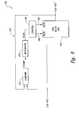
- An example of a conventional variable delay circuit 10is shown in FIG. 1.
- the variable delay circuit 10includes a series of inverters 12 a,b,c,d,e, the first of which 12 a receives a clock signal CLK.
- the output of each inverter 12 a,b,c,d,eis coupled to a respective pass gate 16 a,b,c,d,e that are selectively enabled by respective stages of a shift register 18 . Only one of the stages of the shift register stores a logic “1”, and all of the other stages store a logic “0”.
- the pass gate 16 a,b,c,d,e that receives the logic “1”is enabled while the remaining pass gates 16 a,b,c,d,e that receive a logic “0” are disabled.
- the logic “1”is shifted to the right by applying a shift pulse to a DELAY INCR input of the shift register 18 , and is shifted to the left by applying a shift pulse to a DELAY DECR input of the shift register 18 .
- Outputs of all of the pass gates 16 a,b,c,d,eare coupled to each other to generate a delayed clock signal at a CLK-OUT terminal.
- one of the pass gates 16 a,b,c,d,eis enabled by receiving a logic “1” from the shift register 18 , thereby coupling the output from the respective inverter 12 a,b,c, to the CLK-OUT terminal.
- the magnitude of the delay of the CLK-OUT signalis adjusted by shifting the logic “1” right and left by applying a shift pulse to the DELAY INCR input or DELAY DECR input, respectively, of the shift register 18 .
- variable delay circuit 10 of FIG. 1provides adequate performance under some circumstances, it has the significant disadvantage of inverting the clock signal as the delay is switched from one inverter 12 a,b,c,d,e to the next. More specifically, for example, when the logic “1” is shifted from the pass gate 16 b to the pass gate 16 c , the delay of CLK-OUT signal shifts by not only the additional delay of the inverter 12 c , but, because of the additional inversion caused by passing though the inverter, an additional delay of one-half the period of the CLK signal. This additional delay can be a significant problem in some applications.
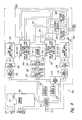
- variable delay circuit 30uses many of the same components used in the variable delay circuit 10 of FIG. 1, and these components have been provided with the same reference numerals.
- the delay circuit 30differs from the delay circuit 10 by including an additional series of inverters 32 a,b,c,d,e, the first of which 32 a receives CLK*, which is the compliment of the CLK signal.
- connection to the pass gates 16 a,b,c,d,ethen alternate between the inverters 12 a,b,c,d,e and the inverters 32 a,b,c,d,e so all of the pass gates 16 a,b,c,d,e receive the same phase of the clock signal.
- the delay of the CLK-OUT signalvaries by only the delay of the additional inverter 12 or 32 .
- variable delay circuit 30avoids the major problem with the delay circuit 10 , it does so at the expense of doubling the number of required inverters.
- the extra circuitry and consequent expense of these additional inverterscan be significant, particularly where a large number of inverters are need to provide a large delay or a large number of delay increments.
- a variable delay circuitproduces a delayed clock signal from an input clock signal by coupling the input clock signal through a plurality of inverting logic circuits arranged in series with each other.
- a delay select circuitsuch as a shift register, receives at least one delay command signal indicative of a delay of the variable delay circuit. The delay select circuit then generates at least one control signal responsive to the delay command signal.
- the variable delay circuitalso includes a clock transfer control circuit coupled to the inverting logic circuits and the delay select circuit. The clock transfer control circuit receives the input clock signal and adjusts the delay of the delayed clock signal responsive to the at least one control signal. The delay is adjusted by varying the number of inverting logic circuits through which the input clock signal is coupled between the clock input terminal and the clock output terminal.
- the clock transfer control circuitalso adjusts the polarity of the input clock signal between the clock input terminal and the clock output terminal as a function of the at least one control signal so that the correct polarity of the delayed clock signal is maintained despite being coupled through a variable number of inverting logic circuits.
- FIG. 1is a logic diagram showing a conventional variable delay circuit.
- FIG. 2is a logic diagram showing another conventional variable delay circuit.
- FIG. 3is a block diagram showing one embodiment of a variable delay circuit according to the present invention.
- FIG. 4is a logic diagram showing one embodiment of the variable delay circuit of FIG. 3.
- FIG. 5is a logic diagram showing one embodiment of a clock polarity control circuit used in the variable delay circuit of FIG. 4.
- FIG. 6is a logic diagram showing another embodiment of a clock polarity control circuit used in the variable delay circuit of FIG. 4.
- FIG. 7is a logic diagram showing another embodiment of the variable delay circuit of FIG. 3.
- FIG. 8is a block diagram of a delay-locked loop using one or more of the variable delay circuit embodiments according to the present invention.
- FIG. 9is a block diagram of a memory device using one or more of the variable delay circuit embodiments, or a delay-locked loop using one or more of the variable delay circuit embodiments, according to the present invention.
- FIG. 10is a block diagram of a computer system using the memory device of FIG. 9.
- FIG. 3is a block diagram of one embodiment of a variable delay circuit 40 according to the present invention.
- the delay circuit 40included a clock transfer control circuit 44 to which an incoming clock signal CLK-IN is applied and from which a delayed clock signal CLK-OUT is generated.
- the transfer control circuit 44also receives DELAY INCR and DELAY DECR pulses that are also applied to a delay select circuit 46 .
- the clock transfer circuit 44is coupled to the delay select circuit 46 and to a plurality of inverting logic circuits 48 a,b,c,d.
- the delay select circuit 46outputs a signal on one of its interconnections to the clock transfer circuit 44 that selects the magnitude of the delay of the CLK-OUT signal.
- the interconnection on which the select signal is generatedis shifted in one direction to increase the delay responsive to each DELAY INCR pulse, and is shifted in the other direction to decrease the delay responsive to each DELAY DECR pulse.
- the select signalmay be, for example, a logic “1” signal.
- the transfer control circuit 44transfers the CLK-IN signal to one of the inverting logic circuits 48 and transfers the CLK-OUT signal from one of the inverting logic circuits.
- the transfer control circuit 44does so by selecting the entry point for the CLK-IN signal and/or the exit point of the CLK-OUT signal in the chain of inverting logic circuits 48 .
- the CLK-IN signalmay be applied to the first inverting logic circuit 48 a, and the delay select circuit 46 may cause the clock transfer control circuit 44 to couple the output of the inverting logic circuit 48 c to the CLK-OUT terminal.
- the delay select circuit 46In response to a DELAY INCR pulse, the delay select circuit 46 causes the clock transfer control circuit 44 to couple the output of the inverting logic circuit 48 d to the CLK-OUT terminal. In response to a DELAY DECR pulse, the delay select circuit 46 causes the clock transfer control circuit 44 to couple the output of the inverting logic circuit 48 b to the CLK-OUT terminal. Alternatively, for example, the clock transfer control circuit 44 may couple the output of the inverting logic circuit 48 d to the CLK-OUT terminal, and may vary the inverting logic circuit 48 to which the CLK-IN signal is applied. For example, the delay select circuit 46 may cause the clock transfer control circuit 44 to couple the CLK-IN signal to the second inverting logic circuit 48 b .
- the delay select circuit 46In response to a DELAY INCR pulse, the delay select circuit 46 causes the clock transfer control circuit 44 to couple the CLK-IN signal to the input of the first inverting logic circuit 48 a . In response to a DELAY DECR pulse, the delay select circuit 46 causes the clock transfer control circuit 44 to couple the CLK-IN signal to the input of the third inverting logic circuit 48 c . The delay select circuit 46 may also causes the clock transfer control circuit 44 to adjust both the inverting logic circuit 48 to which the CLK-IN signal is applied and the inverting logic circuit 48 from which the CLK-OUT signal is taken.
- variable delay circuit 40If the operation of the variable delay circuit 40 was limited to the operation described above, it would exhibit the same problem as the variable delay circuit 10 of FIG. 1. Specifically, the delay of the CLK-OUT signal would increment and decrement by the sum of the delay of each inverting logic circuit 48 and one-half the period of the CLK-IN signal. To prevent these unwanted inversions, the clock transfer control circuit 44 either inverts the CLK-IN signal or the CLK-OUT signal each time it alters the inverting logic circuit 48 to which the CLK-IN signal is applied and/or from which the CLK-OUT signal is derived. For example, the clock transfer control circuit 44 may initially apply the CLK-IN signal to the inverting logic circuit 48 b .
- the clock transfer control circuit 44In response to a DELAY NCR pulse, the clock transfer control circuit 44 either applies the compliment of the CLK-IN signal to the inverting logic circuit 48 a or inverts the signal coupled from the inverting logic circuit 48 d to derive the CLK-OUT signal so the phase of the CLK-OUT signal remains constant. As a result, the delay of the CLK-OUT signal increases by only the delay of a single inverting logic circuit 48 .
- the clock transfer control circuit 44operates in a similar manner when changing the inverting logic circuit 48 from which the CLK-OUT signal is derived.
- the clock transfer control circuit 44may initially derive the CLK-OUT signal from the inverting logic circuit 48 c .
- the clock transfer control circuit 44derives the CLK-OUT signal from the inverting logic circuit 48 b , and inverts either the CLK-IN signal before it is applied to one of the inverting logic circuit or the signal coupled from one of the inverting logic circuits 48 that is used to derive the CLK-OUT signal.
- variable delay circuit 40may be implemented with a variety of circuitry, one embodiment of which is shown in FIG. 4.
- a variable delay circuit 50includes a shift register 52 as the delay select circuit 46 , and a plurality of inverters 56 a,b,c,d,e as the inverting logic circuits 48 .
- inverting logic circuits other than the inverters 56 a,b,c,d,esuch as NOR-gates and NAND-gates (not shown), may be used.
- the clock transfer control circuit 44includes a set of pass gates 58 a,b,c,d,e that selectively couple the outputs of respective inverters 56 a,b,c,d,e to a CLK-OUT terminal.
- the operation of the shift register 40 , pass gates 58 a,b,c,d,e and inverters 56 a,b,c,d,eare essentially as described above with reference to FIG. 1 for the shift register 18 , pass gates 16 a,b,c,d,e and inverters 12 a,b,c,d,e.
- the clock transfer control circuit 44also includes a polarity control circuit 60 that selectively inverts the CLK-IN signal before it is applied to one of the inverters 56 .
- the polarity control circuit 60receives the DELAY INCR and DELAY DECR pulses, as well as the CLK-IN signal, and is operable to alter the inversion of the CLK-IN signal responsive to each DELAY INCR or DELAY DECR pulse before applying the CLK-IN signal or its compliment to the inverter 56 a .
- the polarity control circuit 60may initially not invert the CLK-IN signal before coupling it to the input of the inverter 56 a .
- the polarity control circuit 60In response to either a DELAY INCR pulse or a DELAY DECR pulse, the polarity control circuit 60 inverts the CLK-IN signal before coupling it to the input of the inverter 56 a . As a result, the CLK-IN signal is inverted each time the pass gates 58 change the inverter 56 from which the CLK-OUT signal is derived. The delay of the CLK-OUT signal thus changes responsive to each DELAY INCR pulse or a DELAY DECR pulse by only the delay of a single inverter 56 . In this manner, the variable delay circuit 40 is able to prevent unwanted inversions of clock signal without using a second set of inverters, thereby using relatively little circuitry.
- circuitry for the polarity control circuit 60must be added to the circuitry used in the prior art variable delay circuit 10 of FIG. 1, the amount of circuitry needed to implement the polarity control circuit 60 does not increase with the number of inverters 56 . The amount of circuitry needed for the polarity control circuit 60 is thus relatively little in the event a large number of inverters are needed to provide a large number of delay values.
- FIG. 5One embodiment of a polarity control circuit 60 ′ using an exclusive NOR-gate 68 and a clock polarity selector 64 ′ is shown in FIG. 5.
- the clock polarity selector 64 ′includes an NOR-gate 70 having inputs coupled to receive both DELAY INCR and DELAY DECR pulses, thereby clocking a flip-flop 72 .
- a Q output of the flip-flop 72is coupled to its data input D through an inverter 78 .
- the Q output of the flip-floptoggles from logic “0” to logic “1” and vice-versa responsive to each DELAY INCR and DELAY DECR pulse.
- the Q output of the flip-flop 72is applied to one input of the exclusive NOR-gate 68 , which also receives the CLK-IN signal at its other input.
- the flip-flop 72thus causes the exclusive NOR-gate 68 to alter its inverting function responsive to each DELAY INCR or DELAY DECR pulse.
- the flip-flop 72may initially apply a logic “ 0 ” to the exclusive NOR-gate 68 so that the exclusive NOR-gate does not invert the CLK-IN signal before coupling it to the input of the inverter 56 a .
- the flip-flop 72In response to either a DELAY INCR pulse or a DELAY DECR pulse, the flip-flop 72 applies a logic “1” to the exclusive NOR-gate 68 , thereby causing it to invert the CLK-IN signal before coupling it to the input of the inverter 56 a .
- the CLK-IN signalis inverted each time the pass gates 58 change the inverter 56 from which the CLK-OUT signal is derived.
- the delay of the CLK-OUT signalthus changes responsive to each DELAY INCR pulse or a DELAY DECR pulse by only the delay of a single inverter 56 .
- FIG. 6Another embodiment of a polarity control circuit 60 ′′ is shown in FIG. 6.
- the polarity control circuit 60 ′′uses the clock polarity selector 64 ′ of FIG. 5.
- the polarity control circuit 60 ′′uses a non-inverting clock path formed by a pass gate 80 in parallel with an inverting clock path formed by an inverter 82 coupled in series with a pass gate 84 .
- the Q output of the flip-flop 72is coupled directly to a control input of the pass gate 80 and to the control input of the pass gate 84 through an inverter 88 .
- the pass gates 80 , 84are alternately enabled, and the particular pass gate 80 , 84 that is enabled changes each time the Q output of the flip-flop 72 toggles.
- the pass gate 80is enabled, the CLK-IN signal is coupled directly to the inverter 56 a (FIG. 4).
- the pass gate 84is enabled, the CLK-IN signal is inverted before being coupled to the inverter 56 a so that the inverter 56 a receives the compliment of the CLK-IN signal.
- variable delay circuit 100Another embodiment of a variable delay circuit 100 according to the present invention is shown in FIG. 7. Unlike the variable delay circuit 50 of FIG. 4, the variable delay circuit varies the delay of the CLK-OUT signal by varying the entry point of the CLK-IN signal into the chain of inverting logic circuits 48 (FIG. 3). With reference to FIG. 7, the variable delay circuit 100 includes as the delay select circuit 46 a shift register 104 receiving DELAY INCR and DELAY DECR pulses, as previously explained. However, the DELAY INCR and DELAY DECR pulses shift the logic “1” in directions opposite the directions they shift the logic “1” in the shift register 52 of FIG.
- variable delay circuit 100also includes as the inverting logic circuits 48 a series of alternating NOR-gates 110 a,b,c and NAND-gates 112 a,b,c .
- the clock transfer control circuit 44is implemented by a plurality of NOR-gates 120 a,b,c alternating with a plurality of NAND-gates 122 a,b,c .
- each NOR-gate 120 a,b,cis coupled to an input of a respective NOR gate 110 a,b,c, and the output of each of the NAND-gates 122 a,b,c is coupled to an input of a respective NAND-gate 112 a,b,c .
- Each of the NAND-gates 122 a,b,c in the clock transfer control circuit 44receives a control input from the Q output of a respective stage of the shift register 104 .
- Each of the NOR-gates 120 a,b,c in the clock transfer control circuit 44receives a control input from the Q* output of a respective stage of the shift register 104 .
- each of the NOR-gates 120 a,b,calso receives the CLK-IN signal, and each of the NAND-gates 122 a,b,c receives the compliment of the CLK-IN signal generated by applying the CLK-IN signal to an inverter 128 .
- variable delay circuit 100The operation of the variable delay circuit 100 will now be explained assuming the stage of the shift register 104 coupled to the NAND-gate 122 b is storing a logic “1”.
- the logic “1” applied to the NAND-gate 122 benables the gate 122 b , thereby allowing the CLK-IN* signal to be coupled through the NAND-gate 122 b .
- each of the other NAND-gates 122 a,creceives a logic “0”, thereby disabling the gates 122 a,c and causing them to output a logic “1” to a respective NAND-gate 112 a,c .
- each of the other NOR-gates 120 a,b,creceives a logic “1”, thereby disabling the gates 120 a,b,c and causing them to output a logic “0” to a respective NOR-gate 110 a,b,c .
- all of the gates 110 , 112 in the delay chainare enabled.
- the CLK-IN* signal coupled through the NAND-gate 122 bis coupled through the NAND-gate 112 b , the NOR-gate 110 b , the NAND-gate 112 c , and the NOR-gate 110 c before being applied to the CLK-OUT terminal.
- inverting logic circuitsi.e., inverter 128 and gates 122 b , 112 b , 100 b , 112 c , 110 c , between the CLK-IN terminal and the CLK-OUT terminal so that the CLK-OUT signal is a delayed but non-inverted replica of the CLK-IN signal.
- the shift register 104receives a DELAY INCR pulse
- the stage storing a logic “1”shifts to the left so the NOR-gate 120 a receives a logic “0” to enable it to pass the CLK-IN signal.
- each of the other NAND-gates 122 a,b,creceives a logic “0”, thereby disabling the gates 122 a,b,c and causing them to output a logic “1” to enable a respective NAND-gate 112 a,b,c .
- each of the other NOR-gates 120 b,creceives a logic “1”, thereby disabling the gates 120 b,c and causing them to output a logic “0” to enable a respective NOR-gate 110 b,c .
- the CLK-IN signal coupled through the NOR-gate 120 ais coupled through the NOR-gate 110 a , the NAND-gate 112 b , the NOR-gate 110 b , the NAND-gate 112 c , and the NOR-gate 110 c before being applied to the CLK-OUT terminal.
- variable delay circuitresponds in a similar manner to DELAY DECR pulses.
- variable delay lines 40 , 50 , 100may be used in a variety of circuits, including a delay-locked loop, such as the delay-locked loop 150 shown in FIG. 8.
- a clock reference signal CLK-REFis applied to a variable delay line 154 , which may be one of the variable delay lines 40 , 50 , 100 or some other variable delay line in accordance with the invention.
- an clock output signal CLK-OUTis output from the variable delay line 154 with a delay that is determined by a INCR control pulses on line 160 and DECR control pulses on line 162 .
- a feedback loop 170formed by a comparator 172 , an integrator 174 and a control circuit 178 of conventional design, produces the INCR and DECR control pulses.
- the feedback loop 170receives the clock reference signal CLK-REF at one input of the comparator 172 and receives the clock output signal CLK-OUT from the variable delay line 154 as a feedback signal at the other input of the comparator 172 .
- the comparator 172outputs a compare pulses VCOMP that are integrated by the integrator 174 to apply a control signal VCON to the control circuit 178 .
- the control circuit 178then produces the INCR and DECR control pulses to maintain a predetermined relationship between the phase of the clock reference signal CLK-REF and the clock output signal CLK-OUT.
- control signal VCONwill depend upon the relative phases of the clock reference signal CLK-REF and the clock output signal CLK-OUT. If the clock output signal CLK-OUT leads the clock reference signal CLK-REF, the control signal VCON causes the control circuit 178 to apply INCR pulses to the variable delay line 154 to increase the delay of the variable delay line 154 until the clock output signal CLK-OUT is in phase with the clock reference signal CLK-REF.
- the control signal VCONcauses the control circuit 178 to apply DECR pulses to the variable delay line 154 to decrease the delay of the variable delay line 154 until the clock output signal CLK-OUT is in phase with the clock reference signal CLK-REF.
- FIG. 8is shown in the context of a delay-locked loop, it will be understood it can be used in other types of locked-loops, such as phase-locked loops.
- variable delay line 154which may be the variable delay lines 40 , 50 , 100 , is shown in FIG. 8 in the context of a delay-locked loop, it will be understood it can be used in other types of locked-loops, such as phase-locked loops, as well as in a wide variety of digital circuits.
- the variable delay lines in accordance with the inventionmay be used in a memory device, such as a synchronous dynamic random access memory (“SDRAM”) 200 shown in FIG. 9.
- SDRAMsynchronous dynamic random access memory
- the delay-locked loop 150 shown in FIG. 8may be used the SDRAM 200 as well as in a variety of other circuits.
- the memory device illustrated thereinis a synchronous dynamic random access memory (“SDRAM”) 200 , although the invention can be embodied in other types of synchronous DRAMs, such as packetized DRAMs and RAMBUS DRAMs (RDRAMS′′), as well as other types of digital devices.
- SDRAM 200includes an address register 212 that receives either a row address or a column address on an address bus 214 .
- the address bus 214is generally coupled to a memory controller (not shown).
- a row addressis initially received by the address register 212 and applied to a row address multiplexer 218 .
- the row address multiplexer 218couples the row address to a number of components associated with either of two memory banks 220 , 222 depending upon the state of a bank address bit forming part of the row address. Associated with each of the memory banks 220 , 222 is a respective row address latch 226 , which stores the row address, and a row decoder 228 , which applies various signals to its respective array 220 or 222 as a function of the stored row address.
- the row address multiplexer 218also couples row addresses to the row address latches 226 for the purpose of refreshing the memory cells in the arrays 220 , 222 .
- the row addressesare generated for refresh purposes by a refresh counter 230 , which is controlled by a refresh controller 232 .
- a column addressis applied to the address register 212 .
- the address register 212couples the column address to a column address latch 240 .
- the column addressis either coupled through a burst counter 242 to a column address buffer 244 , or to the burst counter 242 which applies a sequence of column addresses to the column address buffer 244 starting at the column address output by the address register 212 .
- the column address buffer 244applies a column address to a column decoder 248 which applies various signals to respective sense amplifiers and associated column circuitry 250 , 252 for the respective arrays 220 , 222 .
- Data to be read from one of the arrays 220 , 222is coupled to the column circuitry 250 , 252 for one of the arrays 220 , 222 , respectively.
- the datais then coupled through a read data path 254 to a data output register 256 , which applies the data to a data bus 258 .
- Data to be written to one of the arrays 220 , 222is coupled from the data bus 258 , a data input register 260 and a write data path 262 to the column circuitry 250 , 252 where it is transferred to one of the arrays 220 , 222 , respectively.
- a mask register 264may be used to selectively alter the flow of data into and out of the column circuitry 250 , 252 , such as by selectively masking data to be read from the arrays 220 , 222 .
- a command decoder 268responsive to command signals received on a control bus 270 .
- These high level command signalsare a clock enable signal CKE*, a clock signal CLK, a chip select signal CS*, a write enable signal WE*, a row address strobe signal RAS*, and a column address strobe signal CAS*, which the “* ” designating the signal as active low.
- Various combinations of these signalsare registered as respective commands, such as a read command or a write command.
- the command decoder 268generates a sequence of control signals responsive to the command signals to carry out the function (e.g., a read or a write) designated by each of the command signals.
- the CLK signalmay be used to generate an internal clock signal ICLK by coupling the CLK signal to a clock generator circuit 272 that uses one or more of the variable delay lines 40 , 50 , 100 in accordance with various embodiments of the invention.
- the clock generator circuit 272may also use the delay-locked loop 150 shown in FIG. 8 or some other delay-locked loop using one or more of the variable delay lines 40 , 50 , 100 .
- FIG. 10shows a computer system 300 containing the SDRAM 200 of FIG. 9.
- the computer system 300includes a processor 302 for performing various computing functions, such as executing specific software to perform specific calculations or tasks.
- the processor 302includes a processor bus 304 that normally includes an address bus, a control bus, and a data bus.
- the computer system 300includes one or more input devices 314 , such as a keyboard or a mouse, coupled to the processor 302 to allow an operator to interface with the computer system 300 .
- the computer system 300also includes one or more output devices 316 coupled to the processor 302 , such output devices typically being a printer or a video terminal.
- One or more data storage devices 318are also typically coupled to the processor 302 to allow the processor 302 to store data in or retrieve data from internal or external storage media (not shown). Examples of typical storage devices 318 include hard and floppy disks, tape cassettes, and compact disk read-only memories (CD-ROMs).
- the processor 302is also typically coupled to cache memory 326 , which is usually static random access memory (“SRAM”), and to the SDRAM 200 through a memory controller 330 .
- the memory controller 330normally includes a control bus 336 and an address bus 338 that are coupled to the SDRAM 200 .
- a data bus 340is coupled from the SDRAM 200 to the processor bus 304 either directly (as shown), through the memory controller 330 , or by some other means.
Landscapes
- Pulse Circuits (AREA)
- Dram (AREA)
Abstract
Description
- The invention relates clock circuits, and, more particularly, to a circuit and method for providing a clock signal with a variable delay in a manner that uses relatively little circuitry.[0001]
- Variable delay circuits for delaying digital signals are in common use in a wide variety of integrated circuit devices. For example, variable delay circuits are commonly used as part of delay locked loops in integrated circuit memory devices. An example of a conventional[0002]
variable delay circuit 10 is shown in FIG. 1. Thevariable delay circuit 10 includes a series ofinverters 12a,b,c,d,e,the first of which12areceives a clock signal CLK. The output of eachinverter 12a,b,c,d,e iscoupled to arespective pass gate 16a,b,c,d,ethat are selectively enabled by respective stages of ashift register 18. Only one of the stages of the shift register stores a logic “1”, and all of the other stages store a logic “0”. Thepass gate 16a,b,c,d,ethat receives the logic “1” is enabled while theremaining pass gates 16a,b,c,d,ethat receive a logic “0” are disabled. The logic “1” is shifted to the right by applying a shift pulse to a DELAY INCR input of theshift register 18, and is shifted to the left by applying a shift pulse to a DELAY DECR input of theshift register 18. Outputs of all of thepass gates 16a,b,c,d,eare coupled to each other to generate a delayed clock signal at a CLK-OUT terminal. - In operation, one of the[0003]
pass gates 16a,b,c,d,eis enabled by receiving a logic “1” from theshift register 18, thereby coupling the output from therespective inverter 12a,b,c,to the CLK-OUT terminal. The magnitude of the delay of the CLK-OUT signal is adjusted by shifting the logic “1” right and left by applying a shift pulse to the DELAY INCR input or DELAY DECR input, respectively, of theshift register 18. - Although the[0004]
variable delay circuit 10 of FIG. 1 provides adequate performance under some circumstances, it has the significant disadvantage of inverting the clock signal as the delay is switched from oneinverter 12a,b,c,d,eto the next. More specifically, for example, when the logic “1” is shifted from thepass gate 16bto thepass gate 16c, the delay of CLK-OUT signal shifts by not only the additional delay of theinverter 12c, but, because of the additional inversion caused by passing though the inverter, an additional delay of one-half the period of the CLK signal. This additional delay can be a significant problem in some applications. - The above-described problem with the conventional[0005]
variable delay circuit 10 is well recognized, and has been solved to some extent by using avariable delay circuit 30 as shown in FIG. 2. Thevariable delay circuit 30 uses many of the same components used in thevariable delay circuit 10 of FIG. 1, and these components have been provided with the same reference numerals. Thedelay circuit 30 differs from thedelay circuit 10 by including an additional series ofinverters 32a,b,c,d,e,the first of which32areceives CLK*, which is the compliment of the CLK signal. The connections to thepass gates 16a,b,c,d,ethen alternate between theinverters 12a,b,c,d,eand theinverters 32a,b,c,d,eso all of thepass gates 16a,b,c,d,ereceive the same phase of the clock signal. As a result, when the logic “1” is shifted from onepass gate 16a,b,c,d,eto the next, the delay of the CLK-OUT signal varies by only the delay of theadditional inverter 12 or32. - Although the[0006]
variable delay circuit 30 avoids the major problem with thedelay circuit 10, it does so at the expense of doubling the number of required inverters. The extra circuitry and consequent expense of these additional inverters can be significant, particularly where a large number of inverters are need to provide a large delay or a large number of delay increments. - There is therefore a need for a variable delay circuit that avoids the problem of inverting the clock signal from one stage to the next, but does so in a manner that does not require a doubling of the number of inverters needed to achieve a desired delay or a number of delay increments.[0007]
- A variable delay circuit produces a delayed clock signal from an input clock signal by coupling the input clock signal through a plurality of inverting logic circuits arranged in series with each other. A delay select circuit, such as a shift register, receives at least one delay command signal indicative of a delay of the variable delay circuit. The delay select circuit then generates at least one control signal responsive to the delay command signal. The variable delay circuit also includes a clock transfer control circuit coupled to the inverting logic circuits and the delay select circuit. The clock transfer control circuit receives the input clock signal and adjusts the delay of the delayed clock signal responsive to the at least one control signal. The delay is adjusted by varying the number of inverting logic circuits through which the input clock signal is coupled between the clock input terminal and the clock output terminal. The clock transfer control circuit also adjusts the polarity of the input clock signal between the clock input terminal and the clock output terminal as a function of the at least one control signal so that the correct polarity of the delayed clock signal is maintained despite being coupled through a variable number of inverting logic circuits.[0008]
- FIG. 1 is a logic diagram showing a conventional variable delay circuit.[0009]
- FIG. 2 is a logic diagram showing another conventional variable delay circuit.[0010]
- FIG. 3 is a block diagram showing one embodiment of a variable delay circuit according to the present invention.[0011]
- FIG. 4 is a logic diagram showing one embodiment of the variable delay circuit of FIG. 3.[0012]
- FIG. 5 is a logic diagram showing one embodiment of a clock polarity control circuit used in the variable delay circuit of FIG. 4.[0013]
- FIG. 6 is a logic diagram showing another embodiment of a clock polarity control circuit used in the variable delay circuit of FIG. 4.[0014]
- FIG. 7 is a logic diagram showing another embodiment of the variable delay circuit of FIG. 3.[0015]
- FIG. 8 is a block diagram of a delay-locked loop using one or more of the variable delay circuit embodiments according to the present invention.[0016]
- FIG. 9 is a block diagram of a memory device using one or more of the variable delay circuit embodiments, or a delay-locked loop using one or more of the variable delay circuit embodiments, according to the present invention.[0017]
- FIG. 10 is a block diagram of a computer system using the memory device of FIG. 9.[0018]
- FIG. 3 is a block diagram of one embodiment of a[0019]
variable delay circuit 40 according to the present invention. Thedelay circuit 40 included a clocktransfer control circuit 44 to which an incoming clock signal CLK-IN is applied and from which a delayed clock signal CLK-OUT is generated. Thetransfer control circuit 44 also receives DELAY INCR and DELAY DECR pulses that are also applied to a delayselect circuit 46. Theclock transfer circuit 44 is coupled to the delayselect circuit 46 and to a plurality of invertinglogic circuits 48a,b,c,d. - In operation, the delay[0020]
select circuit 46 outputs a signal on one of its interconnections to theclock transfer circuit 44 that selects the magnitude of the delay of the CLK-OUT signal. The interconnection on which the select signal is generated is shifted in one direction to increase the delay responsive to each DELAY INCR pulse, and is shifted in the other direction to decrease the delay responsive to each DELAY DECR pulse. The select signal may be, for example, a logic “1” signal. - The[0021]
transfer control circuit 44 transfers the CLK-IN signal to one of the invertinglogic circuits 48 and transfers the CLK-OUT signal from one of the inverting logic circuits. Thetransfer control circuit 44 does so by selecting the entry point for the CLK-IN signal and/or the exit point of the CLK-OUT signal in the chain of invertinglogic circuits 48. For example, the CLK-IN signal may be applied to the first invertinglogic circuit 48a, and the delayselect circuit 46 may cause the clocktransfer control circuit 44 to couple the output of the invertinglogic circuit 48cto the CLK-OUT terminal. In response to a DELAY INCR pulse, the delayselect circuit 46 causes the clocktransfer control circuit 44 to couple the output of the invertinglogic circuit 48dto the CLK-OUT terminal. In response to a DELAY DECR pulse, the delayselect circuit 46 causes the clocktransfer control circuit 44 to couple the output of the invertinglogic circuit 48bto the CLK-OUT terminal. Alternatively, for example, the clocktransfer control circuit 44 may couple the output of the invertinglogic circuit 48dto the CLK-OUT terminal, and may vary the invertinglogic circuit 48 to which the CLK-IN signal is applied. For example, the delayselect circuit 46 may cause the clocktransfer control circuit 44 to couple the CLK-IN signal to the second invertinglogic circuit 48b. In response to a DELAY INCR pulse, the delayselect circuit 46 causes the clocktransfer control circuit 44 to couple the CLK-IN signal to the input of the first invertinglogic circuit 48a. In response to a DELAY DECR pulse, the delayselect circuit 46 causes the clocktransfer control circuit 44 to couple the CLK-IN signal to the input of the third invertinglogic circuit 48c. The delayselect circuit 46 may also causes the clocktransfer control circuit 44 to adjust both the invertinglogic circuit 48 to which the CLK-IN signal is applied and the invertinglogic circuit 48 from which the CLK-OUT signal is taken. - If the operation of the[0022]
variable delay circuit 40 was limited to the operation described above, it would exhibit the same problem as thevariable delay circuit 10 of FIG. 1. Specifically, the delay of the CLK-OUT signal would increment and decrement by the sum of the delay of each invertinglogic circuit 48 and one-half the period of the CLK-IN signal. To prevent these unwanted inversions, the clocktransfer control circuit 44 either inverts the CLK-IN signal or the CLK-OUT signal each time it alters the invertinglogic circuit 48 to which the CLK-IN signal is applied and/or from which the CLK-OUT signal is derived. For example, the clocktransfer control circuit 44 may initially apply the CLK-IN signal to the invertinglogic circuit 48b. In response to a DELAY NCR pulse, the clocktransfer control circuit 44 either applies the compliment of the CLK-IN signal to the invertinglogic circuit 48aor inverts the signal coupled from the invertinglogic circuit 48dto derive the CLK-OUT signal so the phase of the CLK-OUT signal remains constant. As a result, the delay of the CLK-OUT signal increases by only the delay of a singleinverting logic circuit 48. - The clock[0023]
transfer control circuit 44 operates in a similar manner when changing the invertinglogic circuit 48 from which the CLK-OUT signal is derived. For example, the clocktransfer control circuit 44 may initially derive the CLK-OUT signal from the invertinglogic circuit 48c. In response to a DELAY DECR pulse, the clocktransfer control circuit 44 derives the CLK-OUT signal from the invertinglogic circuit 48b, and inverts either the CLK-IN signal before it is applied to one of the inverting logic circuit or the signal coupled from one of the invertinglogic circuits 48 that is used to derive the CLK-OUT signal. - The[0024]
variable delay circuit 40 may be implemented with a variety of circuitry, one embodiment of which is shown in FIG. 4. As shown in FIG. 4, avariable delay circuit 50 includes ashift register 52 as the delayselect circuit 46, and a plurality ofinverters 56a,b,c,d,eas the invertinglogic circuits 48. However, it will be understood that inverting logic circuits other than theinverters 56a,b,c,d,e,such as NOR-gates and NAND-gates (not shown), may be used. The clocktransfer control circuit 44 includes a set ofpass gates 58a,b,c,d,ethat selectively couple the outputs ofrespective inverters 56a,b,c,d,eto a CLK-OUT terminal. The operation of theshift register 40,pass gates 58a,b,c,d,eandinverters 56a,b,c,d,eare essentially as described above with reference to FIG. 1 for theshift register 18,pass gates 16a,b,c,d,eandinverters 12a,b,c,d,e. - The clock[0025]
transfer control circuit 44 also includes apolarity control circuit 60 that selectively inverts the CLK-IN signal before it is applied to one of the inverters56. Thepolarity control circuit 60 receives the DELAY INCR and DELAY DECR pulses, as well as the CLK-IN signal, and is operable to alter the inversion of the CLK-IN signal responsive to each DELAY INCR or DELAY DECR pulse before applying the CLK-IN signal or its compliment to theinverter 56a. For example, thepolarity control circuit 60 may initially not invert the CLK-IN signal before coupling it to the input of theinverter 56a. In response to either a DELAY INCR pulse or a DELAY DECR pulse, thepolarity control circuit 60 inverts the CLK-IN signal before coupling it to the input of theinverter 56a. As a result, the CLK-IN signal is inverted each time thepass gates 58 change the inverter56 from which the CLK-OUT signal is derived. The delay of the CLK-OUT signal thus changes responsive to each DELAY INCR pulse or a DELAY DECR pulse by only the delay of a single inverter56. In this manner, thevariable delay circuit 40 is able to prevent unwanted inversions of clock signal without using a second set of inverters, thereby using relatively little circuitry. Although circuitry for thepolarity control circuit 60 must be added to the circuitry used in the prior artvariable delay circuit 10 of FIG. 1, the amount of circuitry needed to implement thepolarity control circuit 60 does not increase with the number of inverters56. The amount of circuitry needed for thepolarity control circuit 60 is thus relatively little in the event a large number of inverters are needed to provide a large number of delay values. - One embodiment of a[0026]
polarity control circuit 60′ using an exclusive NOR-gate68 and aclock polarity selector 64′ is shown in FIG. 5. Theclock polarity selector 64′ includes an NOR-gate70 having inputs coupled to receive both DELAY INCR and DELAY DECR pulses, thereby clocking a flip-flop 72. A Q output of the flip-flop 72 is coupled to its data input D through aninverter 78. As a result, the Q output of the flip-flop toggles from logic “0” to logic “1” and vice-versa responsive to each DELAY INCR and DELAY DECR pulse. The Q output of the flip-flop 72 is applied to one input of the exclusive NOR-gate68, which also receives the CLK-IN signal at its other input. The flip-flop 72 thus causes the exclusive NOR-gate68 to alter its inverting function responsive to each DELAY INCR or DELAY DECR pulse. For example, the flip-flop 72 may initially apply a logic “0 ” to the exclusive NOR-gate68 so that the exclusive NOR-gate does not invert the CLK-IN signal before coupling it to the input of theinverter 56a. In response to either a DELAY INCR pulse or a DELAY DECR pulse, the flip-flop 72 applies a logic “1” to the exclusive NOR-gate68, thereby causing it to invert the CLK-IN signal before coupling it to the input of theinverter 56a. As a result, the CLK-IN signal is inverted each time thepass gates 58 change the inverter56 from which the CLK-OUT signal is derived. The delay of the CLK-OUT signal thus changes responsive to each DELAY INCR pulse or a DELAY DECR pulse by only the delay of a single inverter56. - Another embodiment of a[0027]
polarity control circuit 60″ is shown in FIG. 6. Thepolarity control circuit 60″ uses theclock polarity selector 64′ of FIG. 5. However, instead of using an exclusive-OR gate, thepolarity control circuit 60″ uses a non-inverting clock path formed by apass gate 80 in parallel with an inverting clock path formed by aninverter 82 coupled in series with apass gate 84. The Q output of the flip-flop 72 is coupled directly to a control input of thepass gate 80 and to the control input of thepass gate 84 through aninverter 88. As a result, thepass gates particular pass gate flop 72 toggles. When thepass gate 80 is enabled, the CLK-IN signal is coupled directly to theinverter 56a(FIG. 4). When thepass gate 84 is enabled, the CLK-IN signal is inverted before being coupled to theinverter 56aso that theinverter 56areceives the compliment of the CLK-IN signal. - Another embodiment of a[0028]
variable delay circuit 100 according to the present invention is shown in FIG. 7. Unlike thevariable delay circuit 50 of FIG. 4, the variable delay circuit varies the delay of the CLK-OUT signal by varying the entry point of the CLK-IN signal into the chain of inverting logic circuits48 (FIG. 3). With reference to FIG. 7, thevariable delay circuit 100 includes as the delay select circuit46 ashift register 104 receiving DELAY INCR and DELAY DECR pulses, as previously explained. However, the DELAY INCR and DELAY DECR pulses shift the logic “1” in directions opposite the directions they shift the logic “1” in theshift register 52 of FIG. 4 since the variable delay circuit alters the entry point into the series of invertinglogic circuits 48 rather than the exit point from the series of invertinglogic circuits 48. Thevariable delay circuit 100 also includes as the invertinglogic circuits 48 a series of alternating NOR-gates 110a,b,cand NAND-gates 112a,b,c. Finally, the clocktransfer control circuit 44 is implemented by a plurality of NOR-gates 120a,b,calternating with a plurality of NAND-gates 122a,b,c. The output of each NOR-gate120a,b,cis coupled to an input of a respective NORgate 110a,b,c,and the output of each of the NAND-gates 122a,b,cis coupled to an input of a respective NAND-gate112a,b,c. Each of the NAND-gates 122a,b,cin the clocktransfer control circuit 44 receives a control input from the Q output of a respective stage of theshift register 104. Each of the NOR-gates 120a,b,cin the clocktransfer control circuit 44 receives a control input from the Q* output of a respective stage of theshift register 104. Thus, when a shift register stage stores a logic “0”, the Q outputs of the stages output a logic “0” and the Q* outputs of the stages output a logic “1”. Each of the NOR-gates 120a,b,calso receives the CLK-IN signal, and each of the NAND-gates 122a,b,creceives the compliment of the CLK-IN signal generated by applying the CLK-IN signal to aninverter 128. - The operation of the[0029]
variable delay circuit 100 will now be explained assuming the stage of theshift register 104 coupled to the NAND-gate122bis storing a logic “1”. The logic “1” applied to the NAND-gate122benables thegate 122b, thereby allowing the CLK-IN* signal to be coupled through the NAND-gate122b. At the same time, each of the other NAND-gates 122a,creceives a logic “0”, thereby disabling thegates 122a,cand causing them to output a logic “1” to a respective NAND-gate112a,c. Additionally, each of the other NOR-gates 120a,b,creceives a logic “1”, thereby disabling thegates 120a,b,cand causing them to output a logic “0” to a respective NOR-gate110a,b,c. Thus, all of the gates110,112 in the delay chain are enabled. As a result, the CLK-IN* signal coupled through the NAND-gate122bis coupled through the NAND-gate112b, the NOR-gate110b, the NAND-gate112c, and the NOR-gate110cbefore being applied to the CLK-OUT terminal. Note that there are an even number of inverting logic circuits, i.e.,inverter 128 andgates - If the[0030]
shift register 104 receives a DELAY INCR pulse, the stage storing a logic “1” shifts to the left so the NOR-gate120areceives a logic “0” to enable it to pass the CLK-IN signal. Again, each of the other NAND-gates 122a,b,creceives a logic “0”, thereby disabling thegates 122a,b,cand causing them to output a logic “1” to enable a respective NAND-gate112a,b,c. Additionally, each of the other NOR-gates 120b,creceives a logic “1”, thereby disabling thegates 120b,cand causing them to output a logic “0” to enable a respective NOR-gate110b,c. The CLK-IN signal coupled through the NOR-gate120ais coupled through the NOR-gate110a, the NAND-gate112b, the NOR-gate110b, the NAND-gate112c, and the NOR-gate110cbefore being applied to the CLK-OUT terminal. Note again that there are still an even number of inverting logic circuits, i.e.,gates - It is thus seen that, by adjusting the polarity of the CLK-IN signal before it is applied to the inverting logic circuits, the delay of the CLK-OUT signal can be adjusted without introducing unwanted inversions of the CLK-IN signal. Further, this is accomplished without using two inverting logic circuits for each stage of the delay line.[0031]
- The[0032]
variable delay lines loop 150 shown in FIG. 8. A clock reference signal CLK-REF is applied to avariable delay line 154, which may be one of thevariable delay lines variable delay line 154 with a delay that is determined by a INCR control pulses online 160 and DECR control pulses online 162. - A[0033]
feedback loop 170, formed by acomparator 172, anintegrator 174 and acontrol circuit 178 of conventional design, produces the INCR and DECR control pulses. Thefeedback loop 170 receives the clock reference signal CLK-REF at one input of thecomparator 172 and receives the clock output signal CLK-OUT from thevariable delay line 154 as a feedback signal at the other input of thecomparator 172. Thecomparator 172 outputs a compare pulses VCOMP that are integrated by theintegrator 174 to apply a control signal VCON to thecontrol circuit 178. Thecontrol circuit 178 then produces the INCR and DECR control pulses to maintain a predetermined relationship between the phase of the clock reference signal CLK-REF and the clock output signal CLK-OUT. - In operation, the control signal VCON will depend upon the relative phases of the clock reference signal CLK-REF and the clock output signal CLK-OUT. If the clock output signal CLK-OUT leads the clock reference signal CLK-REF, the control signal VCON causes the[0034]
control circuit 178 to apply INCR pulses to thevariable delay line 154 to increase the delay of thevariable delay line 154 until the clock output signal CLK-OUT is in phase with the clock reference signal CLK-REF. Similarly, if the clock output signal CLK-OUT lags the clock reference signal CLK-REF, the control signal VCON causes thecontrol circuit 178 to apply DECR pulses to thevariable delay line 154 to decrease the delay of thevariable delay line 154 until the clock output signal CLK-OUT is in phase with the clock reference signal CLK-REF. - is shown in FIG. 8 in the context of a delay-locked loop, it will be understood it can be used in other types of locked-loops, such as phase-locked loops.[0035]
- Although the[0036]
variable delay line 154, which may be thevariable delay lines loop 150 shown in FIG. 8 may be used theSDRAM 200 as well as in a variety of other circuits. The memory device illustrated therein is a synchronous dynamic random access memory (“SDRAM”)200, although the invention can be embodied in other types of synchronous DRAMs, such as packetized DRAMs and RAMBUS DRAMs (RDRAMS″), as well as other types of digital devices. TheSDRAM 200 includes anaddress register 212 that receives either a row address or a column address on anaddress bus 214. Theaddress bus 214 is generally coupled to a memory controller (not shown). Typically, a row address is initially received by theaddress register 212 and applied to arow address multiplexer 218. Therow address multiplexer 218 couples the row address to a number of components associated with either of twomemory banks memory banks row address latch 226, which stores the row address, and arow decoder 228, which applies various signals to itsrespective array row address multiplexer 218 also couples row addresses to the row address latches226 for the purpose of refreshing the memory cells in thearrays refresh counter 230, which is controlled by arefresh controller 232. - After the row address has been applied to the[0037]
address register 212 and stored in one of the row address latches226, a column address is applied to theaddress register 212. The address register212 couples the column address to acolumn address latch 240. Depending on the operating mode of theSDRAM 200, the column address is either coupled through aburst counter 242 to acolumn address buffer 244, or to theburst counter 242 which applies a sequence of column addresses to thecolumn address buffer 244 starting at the column address output by theaddress register 212. In either case, thecolumn address buffer 244 applies a column address to acolumn decoder 248 which applies various signals to respective sense amplifiers and associatedcolumn circuitry respective arrays - Data to be read from one of the[0038]
arrays column circuitry arrays data path 254 to adata output register 256, which applies the data to adata bus 258. Data to be written to one of thearrays data bus 258, adata input register 260 and a write data path262 to thecolumn circuitry arrays mask register 264 may be used to selectively alter the flow of data into and out of thecolumn circuitry arrays - The above-described operation of the[0039]
SDRAM 200 is controlled by acommand decoder 268 responsive to command signals received on acontrol bus 270. These high level command signals, which are typically generated by a memory controller (not shown), are a clock enable signal CKE*, a clock signal CLK, a chip select signal CS*, a write enable signal WE*, a row address strobe signal RAS*, and a column address strobe signal CAS*, which the “* ” designating the signal as active low. Various combinations of these signals are registered as respective commands, such as a read command or a write command. Thecommand decoder 268 generates a sequence of control signals responsive to the command signals to carry out the function (e.g., a read or a write) designated by each of the command signals. These command signals, and the manner in which they accomplish their respective functions, are conventional. Therefore, in the interest of brevity, a further explanation of these control signals will be omitted. The CLK signal may be used to generate an internal clock signal ICLK by coupling the CLK signal to aclock generator circuit 272 that uses one or more of thevariable delay lines clock generator circuit 272 may also use the delay-lockedloop 150 shown in FIG. 8 or some other delay-locked loop using one or more of thevariable delay lines - FIG. 10 shows a computer system[0040]300 containing the
SDRAM 200 of FIG. 9. The computer system300 includes aprocessor 302 for performing various computing functions, such as executing specific software to perform specific calculations or tasks. Theprocessor 302 includes aprocessor bus 304 that normally includes an address bus, a control bus, and a data bus. In addition, the computer system300 includes one ormore input devices 314, such as a keyboard or a mouse, coupled to theprocessor 302 to allow an operator to interface with the computer system300. Typically, the computer system300 also includes one ormore output devices 316 coupled to theprocessor 302, such output devices typically being a printer or a video terminal. One or moredata storage devices 318 are also typically coupled to theprocessor 302 to allow theprocessor 302 to store data in or retrieve data from internal or external storage media (not shown). Examples oftypical storage devices 318 include hard and floppy disks, tape cassettes, and compact disk read-only memories (CD-ROMs). Theprocessor 302 is also typically coupled tocache memory 326, which is usually static random access memory (“SRAM”), and to theSDRAM 200 through amemory controller 330. Thememory controller 330 normally includes a control bus336 and an address bus338 that are coupled to theSDRAM 200. A data bus340 is coupled from theSDRAM 200 to theprocessor bus 304 either directly (as shown), through thememory controller 330, or by some other means. - From the foregoing it will be appreciated that, although specific embodiments of the invention have been described herein for purposes of illustration, various modifications may be made without deviating from the spirit and scope of the invention. Accordingly, the invention is not limited except as by the appended claims.[0041]
Claims (77)
Priority Applications (4)
| Application Number | Priority Date | Filing Date | Title |
|---|---|---|---|
| US09/943,779US6850107B2 (en) | 2001-08-29 | 2001-08-29 | Variable delay circuit and method, and delay locked loop, memory device and computer system using same |
| US10/268,225US6727734B2 (en) | 2001-08-29 | 2002-10-09 | Variable delay circuit and method, and delay locked loop, memory device and computer system using same |
| US10/272,245US6735148B2 (en) | 2001-08-29 | 2002-10-15 | Variable delay circuit and method, and delay locked loop, memory device and computer system using same |
| US10/272,279US6759883B2 (en) | 2001-08-29 | 2002-10-15 | Variable delay circuit and method, and delay locked loop, memory device and computer system using same |
Applications Claiming Priority (1)
| Application Number | Priority Date | Filing Date | Title |
|---|---|---|---|
| US09/943,779US6850107B2 (en) | 2001-08-29 | 2001-08-29 | Variable delay circuit and method, and delay locked loop, memory device and computer system using same |
Related Child Applications (3)
| Application Number | Title | Priority Date | Filing Date |
|---|---|---|---|
| US10/268,225DivisionUS6727734B2 (en) | 2001-08-29 | 2002-10-09 | Variable delay circuit and method, and delay locked loop, memory device and computer system using same |
| US10/272,245DivisionUS6735148B2 (en) | 2001-08-29 | 2002-10-15 | Variable delay circuit and method, and delay locked loop, memory device and computer system using same |
| US10/272,279DivisionUS6759883B2 (en) | 2001-08-29 | 2002-10-15 | Variable delay circuit and method, and delay locked loop, memory device and computer system using same |
Publications (2)
| Publication Number | Publication Date |
|---|---|
| US20030042960A1true US20030042960A1 (en) | 2003-03-06 |
| US6850107B2 US6850107B2 (en) | 2005-02-01 |
Family
ID=25480243
Family Applications (4)
| Application Number | Title | Priority Date | Filing Date |
|---|---|---|---|
| US09/943,779Expired - Fee RelatedUS6850107B2 (en) | 2001-08-29 | 2001-08-29 | Variable delay circuit and method, and delay locked loop, memory device and computer system using same |
| US10/268,225Expired - Fee RelatedUS6727734B2 (en) | 2001-08-29 | 2002-10-09 | Variable delay circuit and method, and delay locked loop, memory device and computer system using same |
| US10/272,279Expired - Fee RelatedUS6759883B2 (en) | 2001-08-29 | 2002-10-15 | Variable delay circuit and method, and delay locked loop, memory device and computer system using same |
| US10/272,245Expired - Fee RelatedUS6735148B2 (en) | 2001-08-29 | 2002-10-15 | Variable delay circuit and method, and delay locked loop, memory device and computer system using same |
Family Applications After (3)
| Application Number | Title | Priority Date | Filing Date |
|---|---|---|---|
| US10/268,225Expired - Fee RelatedUS6727734B2 (en) | 2001-08-29 | 2002-10-09 | Variable delay circuit and method, and delay locked loop, memory device and computer system using same |
| US10/272,279Expired - Fee RelatedUS6759883B2 (en) | 2001-08-29 | 2002-10-15 | Variable delay circuit and method, and delay locked loop, memory device and computer system using same |
| US10/272,245Expired - Fee RelatedUS6735148B2 (en) | 2001-08-29 | 2002-10-15 | Variable delay circuit and method, and delay locked loop, memory device and computer system using same |
Country Status (1)
| Country | Link |
|---|---|
| US (4) | US6850107B2 (en) |
Cited By (13)
| Publication number | Priority date | Publication date | Assignee | Title |
|---|---|---|---|---|
| US20040003194A1 (en)* | 2002-06-26 | 2004-01-01 | Amit Bodas | Method and apparatus for adjusting DRAM signal timings |
| US20070013425A1 (en)* | 2005-06-30 | 2007-01-18 | Burr James B | Lower minimum retention voltage storage elements |
| US7310008B1 (en)* | 2004-06-08 | 2007-12-18 | Transmeta Corporation | Configurable delay chain with stacked inverter delay elements |
| US20080088343A1 (en)* | 2004-06-08 | 2008-04-17 | Transmeta Corporation | Repeater circuit with high performance repeater mode and normal repeater mode, wherein high performance repeater mode has fast reset capability |
| US20080218215A1 (en)* | 2004-06-08 | 2008-09-11 | Transmeta Corporation | Advanced Repeater Utilizing Signal Distribution Delay |
| US20090045846A1 (en)* | 2004-06-08 | 2009-02-19 | Transmeta Corporation | Advanced repeater with duty cycle adjustment |
| US7498846B1 (en) | 2004-06-08 | 2009-03-03 | Transmeta Corporation | Power efficient multiplexer |
| US7592842B2 (en)* | 2004-12-23 | 2009-09-22 | Robert Paul Masleid | Configurable delay chain with stacked inverter delay elements |
| US7595664B1 (en) | 2004-06-08 | 2009-09-29 | Robert Paul Masleid | Repeater circuit having different operating and reset voltage ranges, and methods thereof |
| US7635992B1 (en) | 2004-06-08 | 2009-12-22 | Robert Paul Masleid | Configurable tapered delay chain with multiple sizes of delay elements |
| US7646228B1 (en) | 2004-06-15 | 2010-01-12 | Masleid Robert P | Inverting zipper repeater circuit |
| US7656212B1 (en) | 2004-06-08 | 2010-02-02 | Robert Paul Masleid | Configurable delay chain with switching control for tail delay elements |
| US20150110157A1 (en)* | 2013-10-23 | 2015-04-23 | Chun-Chi Chen | Time-Domain Temperature Sensing System with a Digital Output and Method Thereof |
Families Citing this family (32)
| Publication number | Priority date | Publication date | Assignee | Title |
|---|---|---|---|---|
| US20030052719A1 (en)* | 2001-09-20 | 2003-03-20 | Na Kwang Jin | Digital delay line and delay locked loop using the digital delay line |
| US7080275B2 (en)* | 2002-08-12 | 2006-07-18 | Micron Technology, Inc. | Method and apparatus using parasitic capacitance for synchronizing signals a device |
| US6999547B2 (en)* | 2002-11-25 | 2006-02-14 | International Business Machines Corporation | Delay-lock-loop with improved accuracy and range |
| US7177170B2 (en)* | 2003-09-17 | 2007-02-13 | Micron Technology, Inc. | Apparatus and method for selectively configuring a memory device using a bi-stable relay |
| US7742887B2 (en)* | 2003-11-24 | 2010-06-22 | Qualcomm Incorporated | Identifying process and temperature of silicon chips |
| US7009407B2 (en)* | 2004-02-19 | 2006-03-07 | Micron Technology, Inc. | Delay lock circuit having self-calibrating loop |
| US7095261B2 (en)* | 2004-05-05 | 2006-08-22 | Micron Technology, Inc. | Clock capture in clock synchronization circuitry |
| US7042260B2 (en)* | 2004-06-14 | 2006-05-09 | Micron Technology, Inc. | Low power and low timing jitter phase-lock loop and method |
| US7276946B2 (en)* | 2004-07-16 | 2007-10-02 | Micron Technology, Inc. | Measure-controlled delay circuits with reduced phase error |
| US7664216B2 (en)* | 2004-08-05 | 2010-02-16 | Micron Technology, Inc. | Digital frequency locked delay line |
| US7583115B2 (en) | 2004-08-26 | 2009-09-01 | Micron Technology, Inc. | Delay line off-state control with power reduction |
| JP4923395B2 (en)* | 2004-08-30 | 2012-04-25 | 富士通株式会社 | Semiconductor circuit, semiconductor circuit characteristic monitoring method, semiconductor circuit test method, semiconductor circuit test apparatus, and semiconductor circuit test program |
| US7348821B2 (en)* | 2004-09-22 | 2008-03-25 | Intel Corporation | Programmable high-resolution timing jitter injectors high-resolution timing jitter injectors |
| US7173468B2 (en)* | 2004-09-27 | 2007-02-06 | Synopsys, Inc. | Multiple-input, single-exit delay line architecture |
| US8816742B2 (en)* | 2004-11-05 | 2014-08-26 | Qualcomm Incorporated | Adaptive memory calibration using bins |
| JP4814248B2 (en)* | 2004-11-05 | 2011-11-16 | クゥアルコム・インコーポレイテッド | Integrated circuits with adaptive speed range. |
| US8164368B2 (en)* | 2005-04-19 | 2012-04-24 | Micron Technology, Inc. | Power savings mode for memory systems |
| US7471130B2 (en) | 2005-05-19 | 2008-12-30 | Micron Technology, Inc. | Graduated delay line for increased clock skew correction circuit operating range |
| US7489172B2 (en)* | 2005-09-29 | 2009-02-10 | Hynix Semiconductor Inc. | DLL driver control circuit |
| US7245245B2 (en)* | 2005-10-11 | 2007-07-17 | Via Technologies Inc. | Digitizer and related charge pump circuit |
| US7417478B2 (en)* | 2006-02-06 | 2008-08-26 | Micron Technology, Inc. | Delay line circuit |
| US7831854B2 (en)* | 2006-03-21 | 2010-11-09 | Mediatek, Inc. | Embedded system for compensating setup time violation and method thereof |
| US20080089126A1 (en)* | 2006-09-29 | 2008-04-17 | Texas Instruments Incorporated | Circuitry for reliability testing as a function of slew |
| US7865756B2 (en)* | 2007-03-12 | 2011-01-04 | Mosaid Technologies Incorporated | Methods and apparatus for clock signal synchronization in a configuration of series-connected semiconductor devices |
| US7932756B2 (en)* | 2007-08-01 | 2011-04-26 | Texas Instruments Incorporated | Master slave delay locked loops and uses thereof |
| US8795326B2 (en)* | 2007-10-05 | 2014-08-05 | Covidien Lp | Expanding seal anchor for single incision surgery |
| JP5472487B2 (en)* | 2010-11-26 | 2014-04-16 | 富士通株式会社 | Semiconductor device and information processing apparatus |
| US20130002297A1 (en)* | 2011-06-28 | 2013-01-03 | Texas Instruments, Incorporated | Bias temperature instability-resistant circuits |
| US9479151B2 (en) | 2013-10-04 | 2016-10-25 | Micron Technology, Inc. | Apparatuses and methods for controlling delay circuits during an idle state to reduce degradation of an electrical characteristic |
| US10200046B1 (en)* | 2017-02-15 | 2019-02-05 | Intel Corporation | High resolution and low power interpolator for delay chain |
| WO2018160569A1 (en) | 2017-03-01 | 2018-09-07 | Analog Devices Global Unlimited Company | Feedforward phase noise compensation |
| US10608620B2 (en)* | 2018-06-19 | 2020-03-31 | Micron Technology, Inc. | Shifter circuits having registers arranged in a folded topology |
Family Cites Families (42)
| Publication number | Priority date | Publication date | Assignee | Title |
|---|---|---|---|---|
| US4255790A (en) | 1978-09-25 | 1981-03-10 | Hondeghem Luc M | Programmable pulse generating system |
| US4458165A (en) | 1983-03-23 | 1984-07-03 | Tektronix, Inc. | Programmable delay circuit |
| US5118975A (en) | 1990-03-05 | 1992-06-02 | Thinking Machines Corporation | Digital clock buffer circuit providing controllable delay |
| JP3605122B2 (en) | 1991-12-13 | 2004-12-22 | テキサス インスツルメンツ インコーポレイテツド | Compensation circuit and method of compensating for delay |
| US5336939A (en) | 1992-05-08 | 1994-08-09 | Cyrix Corporation | Stable internal clock generation for an integrated circuit |
| US5544203A (en) | 1993-02-17 | 1996-08-06 | Texas Instruments Incorporated | Fine resolution digital delay line with coarse and fine adjustment stages |
| US5463337A (en) | 1993-11-30 | 1995-10-31 | At&T Corp. | Delay locked loop based clock synthesizer using a dynamically adjustable number of delay elements therein |
| JPH0897714A (en) | 1994-09-29 | 1996-04-12 | Toshiba Corp | Clock signal generation circuit |
| US5684421A (en) | 1995-10-13 | 1997-11-04 | Credence Systems Corporation | Compensated delay locked loop timing vernier |
| US5744991A (en) | 1995-10-16 | 1998-04-28 | Altera Corporation | System for distributing clocks using a delay lock loop in a programmable logic circuit |
| US5663665A (en) | 1995-11-29 | 1997-09-02 | Cypress Semiconductor Corp. | Means for control limits for delay locked loop |
| KR0179779B1 (en)* | 1995-12-18 | 1999-04-01 | 문정환 | Clock signl modelling circuit |
| US6230245B1 (en) | 1997-02-11 | 2001-05-08 | Micron Technology, Inc. | Method and apparatus for generating a variable sequence of memory device command signals |
| JP3050162B2 (en)* | 1997-04-04 | 2000-06-12 | 日本電気株式会社 | Narrow strike synchronous delay circuit |
| CA2204089C (en) | 1997-04-30 | 2001-08-07 | Mosaid Technologies Incorporated | Digital delay locked loop |
| JPH10313237A (en)* | 1997-05-09 | 1998-11-24 | Nec Corp | Delay circuit device |
| JPH1174783A (en) | 1997-06-18 | 1999-03-16 | Mitsubishi Electric Corp | Internal clock signal generation circuit and synchronous semiconductor memory device |
| US6173432B1 (en) | 1997-06-20 | 2001-01-09 | Micron Technology, Inc. | Method and apparatus for generating a sequence of clock signals |
| US6011732A (en) | 1997-08-20 | 2000-01-04 | Micron Technology, Inc. | Synchronous clock generator including a compound delay-locked loop |
| US6101197A (en) | 1997-09-18 | 2000-08-08 | Micron Technology, Inc. | Method and apparatus for adjusting the timing of signals over fine and coarse ranges |
| US6173424B1 (en) | 1997-12-31 | 2001-01-09 | Micron Technology, Inc. | Programmable pulse generator and method for using same |
| US6175928B1 (en) | 1997-12-31 | 2001-01-16 | Intel Corporation | Reducing timing variance of signals from an electronic device |
| JP3789628B2 (en) | 1998-01-16 | 2006-06-28 | 富士通株式会社 | Semiconductor device |
| US6269451B1 (en) | 1998-02-27 | 2001-07-31 | Micron Technology, Inc. | Method and apparatus for adjusting data timing by delaying clock signal |
| US6175605B1 (en)* | 1998-03-25 | 2001-01-16 | Vanguard International Semiconductor Corporation | Edge triggered delay line, a multiple adjustable delay line circuit, and an application of same |
| JP3727778B2 (en) | 1998-05-07 | 2005-12-14 | 株式会社東芝 | Data high-speed transfer synchronization system and data high-speed transfer synchronization method |
| US6069506A (en)* | 1998-05-20 | 2000-05-30 | Micron Technology, Inc. | Method and apparatus for improving the performance of digital delay locked loop circuits |
| US6016282A (en) | 1998-05-28 | 2000-01-18 | Micron Technology, Inc. | Clock vernier adjustment |
| JP3763673B2 (en) | 1998-06-11 | 2006-04-05 | 富士通株式会社 | DLL circuit |
| US6137334A (en) | 1998-07-06 | 2000-10-24 | Micron Technology, Inc. | Logic circuit delay stage and delay line utilizing same |
| JP3644827B2 (en) | 1998-08-14 | 2005-05-11 | 富士通株式会社 | DLL circuit considering external load |
| US6349399B1 (en) | 1998-09-03 | 2002-02-19 | Micron Technology, Inc. | Method and apparatus for generating expect data from a captured bit pattern, and memory device using same |
| US6201752B1 (en) | 1998-10-01 | 2001-03-13 | Texas Instruments Incorporated | Timing circuit for high voltage testing |
| US6470060B1 (en) | 1999-03-01 | 2002-10-22 | Micron Technology, Inc. | Method and apparatus for generating a phase dependent control signal |
| JP2000306399A (en) | 1999-04-22 | 2000-11-02 | Mitsubishi Electric Corp | Semiconductor device |
| US6255880B1 (en)* | 1999-10-25 | 2001-07-03 | Xilinx, Inc. | One-shot DLL circuit and method |
| US6317381B1 (en) | 1999-12-07 | 2001-11-13 | Micron Technology, Inc. | Method and system for adaptively adjusting control signal timing in a memory device |
| US6417713B1 (en) | 1999-12-30 | 2002-07-09 | Silicon Graphics, Inc. | Programmable differential delay circuit with fine delay adjustment |
| US6518800B2 (en) | 2000-05-31 | 2003-02-11 | Texas Instruments Incorporated | System and method for reducing timing mismatch in sample and hold circuits using the clock |
| US6407687B2 (en) | 2000-06-28 | 2002-06-18 | Texas Instruments Incorporated | System and method for reducing timing mismatch in sample and hold circuits using an FFT and subcircuit reassignment |
| US6586979B2 (en) | 2001-03-23 | 2003-07-01 | Micron Technology, Inc. | Method for noise and power reduction for digital delay lines |
| US6556489B2 (en) | 2001-08-06 | 2003-04-29 | Micron Technology, Inc. | Method and apparatus for determining digital delay line entry point |
- 2001
- 2001-08-29USUS09/943,779patent/US6850107B2/ennot_activeExpired - Fee Related
- 2002
- 2002-10-09USUS10/268,225patent/US6727734B2/ennot_activeExpired - Fee Related
- 2002-10-15USUS10/272,279patent/US6759883B2/ennot_activeExpired - Fee Related
- 2002-10-15USUS10/272,245patent/US6735148B2/ennot_activeExpired - Fee Related
Cited By (33)
| Publication number | Priority date | Publication date | Assignee | Title |
|---|---|---|---|---|
| US20040003194A1 (en)* | 2002-06-26 | 2004-01-01 | Amit Bodas | Method and apparatus for adjusting DRAM signal timings |
| US7656212B1 (en) | 2004-06-08 | 2010-02-02 | Robert Paul Masleid | Configurable delay chain with switching control for tail delay elements |
| US7710160B2 (en) | 2004-06-08 | 2010-05-04 | Masleid Robert P | Stacked inverter delay chain |
| US7332931B1 (en)* | 2004-06-08 | 2008-02-19 | Transmeta Corporation | Leakage efficient anti-glitch filter with variable delay stages |
| US20080088343A1 (en)* | 2004-06-08 | 2008-04-17 | Transmeta Corporation | Repeater circuit with high performance repeater mode and normal repeater mode, wherein high performance repeater mode has fast reset capability |
| US20080143376A1 (en)* | 2004-06-08 | 2008-06-19 | Transmeta Corporation | Leakage efficient anti-glitch filter |
| US20080218215A1 (en)* | 2004-06-08 | 2008-09-11 | Transmeta Corporation | Advanced Repeater Utilizing Signal Distribution Delay |
| US20090045846A1 (en)* | 2004-06-08 | 2009-02-19 | Transmeta Corporation | Advanced repeater with duty cycle adjustment |
| US7498846B1 (en) | 2004-06-08 | 2009-03-03 | Transmeta Corporation | Power efficient multiplexer |
| US7705633B2 (en) | 2004-06-08 | 2010-04-27 | Scott Pitkethly | Advanced repeater with duty cycle adjustment |
| US7592839B2 (en) | 2004-06-08 | 2009-09-22 | Robert Paul Masleid | Repeater circuit with high performance repeater mode and normal repeater mode, wherein high performance repeater mode has fast reset capability |
| US7595664B1 (en) | 2004-06-08 | 2009-09-29 | Robert Paul Masleid | Repeater circuit having different operating and reset voltage ranges, and methods thereof |
| US20090309631A1 (en)* | 2004-06-08 | 2009-12-17 | Robert Paul Masleid | Circuit with enhanced mode and normal mode |
| US7635992B1 (en) | 2004-06-08 | 2009-12-22 | Robert Paul Masleid | Configurable tapered delay chain with multiple sizes of delay elements |
| US9531361B2 (en) | 2004-06-08 | 2016-12-27 | Intellectual Ventures Holding 81 Llc | Power efficient multiplexer |
| US7310008B1 (en)* | 2004-06-08 | 2007-12-18 | Transmeta Corporation | Configurable delay chain with stacked inverter delay elements |
| US7652507B1 (en) | 2004-06-08 | 2010-01-26 | Robert Paul Masleid | Circuits and methods for detecting and assisting wire transitions |
| US9160321B2 (en) | 2004-06-08 | 2015-10-13 | Intellectual Venture Funding Llc | Power efficient multiplexer |
| US8587344B2 (en) | 2004-06-08 | 2013-11-19 | Robert Paul Masleid | Power efficient multiplexer |
| US7724025B2 (en)* | 2004-06-08 | 2010-05-25 | Robert Masleid | Leakage efficient anti-glitch filter |
| US7768295B2 (en) | 2004-06-08 | 2010-08-03 | Scott Pitkethly | Advanced repeater utilizing signal distribution delay |
| US8102190B2 (en) | 2004-06-08 | 2012-01-24 | Robert Paul Masleid | Power efficient multiplexer |
| US8018252B2 (en) | 2004-06-08 | 2011-09-13 | Robert Paul Masleid | Circuit with enhanced mode and normal mode |
| US8008957B2 (en) | 2004-06-15 | 2011-08-30 | Robert Paul Masleid | Inverting zipper repeater circuit |
| US8330515B2 (en) | 2004-06-15 | 2012-12-11 | Robert P Masleid | Inverting zipper repeater circuit |
| US7646228B1 (en) | 2004-06-15 | 2010-01-12 | Masleid Robert P | Inverting zipper repeater circuit |
| US7592842B2 (en)* | 2004-12-23 | 2009-09-22 | Robert Paul Masleid | Configurable delay chain with stacked inverter delay elements |
| US8022731B2 (en) | 2005-06-30 | 2011-09-20 | Scott Pitkethly | Advanced repeater with duty cycle adjustment |
| US20100295577A1 (en)* | 2005-06-30 | 2010-11-25 | Scott Pitkethly | Advanced repeater with duty cycle adjustment |
| US8451025B2 (en) | 2005-06-30 | 2013-05-28 | Scott Pitkethly | Advanced repeater with duty cycle adjustment |
| US20070013425A1 (en)* | 2005-06-30 | 2007-01-18 | Burr James B | Lower minimum retention voltage storage elements |
| US20150110157A1 (en)* | 2013-10-23 | 2015-04-23 | Chun-Chi Chen | Time-Domain Temperature Sensing System with a Digital Output and Method Thereof |
| US9488530B2 (en)* | 2013-10-23 | 2016-11-08 | National Kaohsiung First University Of Science And Technology | Time-domain temperature sensing system with a digital output and method thereof |
Also Published As
| Publication number | Publication date |
|---|---|
| US6735148B2 (en) | 2004-05-11 |
| US20030042961A1 (en) | 2003-03-06 |
| US6850107B2 (en) | 2005-02-01 |
| US20030042952A1 (en) | 2003-03-06 |
| US6727734B2 (en) | 2004-04-27 |
| US20030042951A1 (en) | 2003-03-06 |
| US6759883B2 (en) | 2004-07-06 |
Similar Documents
| Publication | Publication Date | Title |
|---|---|---|
| US6727734B2 (en) | Variable delay circuit and method, and delay locked loop, memory device and computer system using same | |
| US7038971B2 (en) | Multi-clock domain data input-processing device having clock-receiving locked loop and clock signal input method thereof | |
| US7208989B2 (en) | Synchronous clock generator including duty cycle correction | |
| US7042260B2 (en) | Low power and low timing jitter phase-lock loop and method | |
| US7253672B2 (en) | System and method for reduced power open-loop synthesis of output clock signals having a selected phase relative to an input clock signal | |
| US8081020B2 (en) | Delay-lock loop and method adapting itself to operate over a wide frequency range | |
| US6975149B2 (en) | Method and circuit for adjusting the timing of output data based on an operational mode of output drivers | |
| US7224639B2 (en) | Multi-phase clock signal generator and method having inherently unlimited frequency capability | |
| US6737897B2 (en) | Power reduction for delay locked loop circuits | |
| US6194916B1 (en) | Phase comparator circuit for high speed signals in delay locked loop circuit | |
| US7336106B2 (en) | Phase detector and method having hysteresis characteristics | |
| US7428284B2 (en) | Phase detector and method providing rapid locking of delay-lock loops | |
| US20060214710A1 (en) | Delay-lock loop and method having high resolution and wide dynamic range |
Legal Events
| Date | Code | Title | Description |
|---|---|---|---|
| AS | Assignment | Owner name:MICRON TECHNOLOGY, INC., IDAHO Free format text:ASSIGNMENT OF ASSIGNORS INTEREST;ASSIGNOR:GOMM, TYLER J.;REEL/FRAME:012142/0026 Effective date:20010802 | |
| FEPP | Fee payment procedure | Free format text:PAYOR NUMBER ASSIGNED (ORIGINAL EVENT CODE: ASPN); ENTITY STATUS OF PATENT OWNER: LARGE ENTITY | |
| CC | Certificate of correction | ||
| FPAY | Fee payment | Year of fee payment:4 | |
| AS | Assignment | Owner name:ROUND ROCK RESEARCH, LLC,NEW YORK Free format text:ASSIGNMENT OF ASSIGNORS INTEREST;ASSIGNOR:MICRON TECHNOLOGY, INC.;REEL/FRAME:023786/0416 Effective date:20091223 Owner name:ROUND ROCK RESEARCH, LLC, NEW YORK Free format text:ASSIGNMENT OF ASSIGNORS INTEREST;ASSIGNOR:MICRON TECHNOLOGY, INC.;REEL/FRAME:023786/0416 Effective date:20091223 | |
| FPAY | Fee payment | Year of fee payment:8 | |
| REMI | Maintenance fee reminder mailed | ||
| LAPS | Lapse for failure to pay maintenance fees | ||
| STCH | Information on status: patent discontinuation | Free format text:PATENT EXPIRED DUE TO NONPAYMENT OF MAINTENANCE FEES UNDER 37 CFR 1.362 | |
| FP | Lapsed due to failure to pay maintenance fee | Effective date:20170201 |