US20030042534A1 - Scalable flash/NV structures and devices with extended endurance - Google Patents
Scalable flash/NV structures and devices with extended enduranceDownload PDFInfo
- Publication number
- US20030042534A1 US20030042534A1US09/944,985US94498501AUS2003042534A1US 20030042534 A1US20030042534 A1US 20030042534A1US 94498501 AUS94498501 AUS 94498501AUS 2003042534 A1US2003042534 A1US 2003042534A1
- Authority
- US
- United States
- Prior art keywords
- medium
- charge
- injector
- tunnel
- gate stack
- Prior art date
- Legal status (The legal status is an assumption and is not a legal conclusion. Google has not performed a legal analysis and makes no representation as to the accuracy of the status listed.)
- Granted
Links
- 230000000903blocking effectEffects0.000claimsabstractdescription113
- 238000000034methodMethods0.000claimsabstractdescription41
- 230000005641tunnelingEffects0.000claimsabstractdescription24
- XUIMIQQOPSSXEZ-UHFFFAOYSA-NSiliconChemical compound[Si]XUIMIQQOPSSXEZ-UHFFFAOYSA-N0.000claimsdescription101
- 229910052710siliconInorganic materials0.000claimsdescription101
- 239000010703siliconSubstances0.000claimsdescription101
- 239000002159nanocrystalSubstances0.000claimsdescription84
- 239000000758substrateSubstances0.000claimsdescription46
- PNEYBMLMFCGWSK-UHFFFAOYSA-Naluminium oxideInorganic materials[O-2].[O-2].[O-2].[Al+3].[Al+3]PNEYBMLMFCGWSK-UHFFFAOYSA-N0.000claimsdescription45
- VYPSYNLAJGMNEJ-UHFFFAOYSA-NSilicium dioxideChemical compoundO=[Si]=OVYPSYNLAJGMNEJ-UHFFFAOYSA-N0.000claimsdescription44
- 229910052681coesiteInorganic materials0.000claimsdescription21
- 229910052906cristobaliteInorganic materials0.000claimsdescription21
- 239000000377silicon dioxideSubstances0.000claimsdescription21
- 229910052682stishoviteInorganic materials0.000claimsdescription21
- 229910052905tridymiteInorganic materials0.000claimsdescription21
- 230000005684electric fieldEffects0.000claimsdescription19
- 230000006870functionEffects0.000claimsdescription13
- WFKWXMTUELFFGS-UHFFFAOYSA-NtungstenChemical compound[W]WFKWXMTUELFFGS-UHFFFAOYSA-N0.000claimsdescription11
- 229910052721tungstenInorganic materials0.000claimsdescription11
- 239000010937tungstenSubstances0.000claimsdescription11
- PMHQVHHXPFUNSP-UHFFFAOYSA-Mcopper(1+);methylsulfanylmethane;bromideChemical compoundBr[Cu].CSCPMHQVHHXPFUNSP-UHFFFAOYSA-M0.000claimsdescription9
- PCHJSUWPFVWCPO-UHFFFAOYSA-NgoldChemical compound[Au]PCHJSUWPFVWCPO-UHFFFAOYSA-N0.000claimsdescription7
- 239000010931goldSubstances0.000claimsdescription7
- 229910052737goldInorganic materials0.000claimsdescription7
- 238000003491arrayMethods0.000claimsdescription5
- 238000001459lithographyMethods0.000claimsdescription5
- 229910052777PraseodymiumInorganic materials0.000claimsdescription3
- RTAQQCXQSZGOHL-UHFFFAOYSA-NTitaniumChemical compound[Ti]RTAQQCXQSZGOHL-UHFFFAOYSA-N0.000claimsdescription3
- QCWXUUIWCKQGHC-UHFFFAOYSA-NZirconiumChemical compound[Zr]QCWXUUIWCKQGHC-UHFFFAOYSA-N0.000claimsdescription3
- 229910052454barium strontium titanateInorganic materials0.000claimsdescription3
- 229910052735hafniumInorganic materials0.000claimsdescription3
- VBJZVLUMGGDVMO-UHFFFAOYSA-Nhafnium atomChemical compound[Hf]VBJZVLUMGGDVMO-UHFFFAOYSA-N0.000claimsdescription3
- PUDIUYLPXJFUGB-UHFFFAOYSA-Npraseodymium atomChemical compound[Pr]PUDIUYLPXJFUGB-UHFFFAOYSA-N0.000claimsdescription3
- 229910052715tantalumInorganic materials0.000claimsdescription3
- GUVRBAGPIYLISA-UHFFFAOYSA-Ntantalum atomChemical compound[Ta]GUVRBAGPIYLISA-UHFFFAOYSA-N0.000claimsdescription3
- 229910052719titaniumInorganic materials0.000claimsdescription3
- 239000010936titaniumSubstances0.000claimsdescription3
- 229910052726zirconiumInorganic materials0.000claimsdescription3
- 230000002708enhancing effectEffects0.000claims2
- 238000007667floatingMethods0.000description60
- 229910052593corundumInorganic materials0.000description44
- 229910001845yogo sapphireInorganic materials0.000description44
- 238000002347injectionMethods0.000description22
- 239000007924injectionSubstances0.000description22
- 239000000463materialSubstances0.000description21
- 229910052581Si3N4Inorganic materials0.000description18
- 238000005516engineering processMethods0.000description18
- 238000010348incorporationMethods0.000description12
- 230000008878couplingEffects0.000description10
- 238000010168coupling processMethods0.000description10
- 238000005859coupling reactionMethods0.000description10
- 239000012212insulatorSubstances0.000description10
- HQVNEWCFYHHQES-UHFFFAOYSA-Nsilicon nitrideChemical compoundN12[Si]34N5[Si]62N3[Si]51N64HQVNEWCFYHHQES-UHFFFAOYSA-N0.000description10
- 150000004767nitridesChemical class0.000description7
- 238000009792diffusion processMethods0.000description6
- 238000002513implantationMethods0.000description6
- 229910052751metalInorganic materials0.000description5
- 239000002184metalSubstances0.000description5
- 229910021420polycrystalline siliconInorganic materials0.000description5
- 229920005591polysiliconPolymers0.000description5
- 229910003818SiH2Cl2Inorganic materials0.000description4
- 230000004888barrier functionEffects0.000description4
- 230000015556catabolic processEffects0.000description4
- 238000004518low pressure chemical vapour depositionMethods0.000description4
- 230000008569processEffects0.000description4
- 238000000231atomic layer depositionMethods0.000description3
- 230000000694effectsEffects0.000description3
- 230000005669field effectEffects0.000description3
- 238000012545processingMethods0.000description3
- 230000009467reductionEffects0.000description3
- 239000003990capacitorSubstances0.000description2
- 239000004020conductorSubstances0.000description2
- 239000002784hot electronSubstances0.000description2
- 230000014759maintenance of locationEffects0.000description2
- BPUBBGLMJRNUCC-UHFFFAOYSA-Noxygen(2-);tantalum(5+)Chemical compound[O-2].[O-2].[O-2].[O-2].[O-2].[Ta+5].[Ta+5]BPUBBGLMJRNUCC-UHFFFAOYSA-N0.000description2
- RVTZCBVAJQQJTK-UHFFFAOYSA-Noxygen(2-);zirconium(4+)Chemical compound[O-2].[O-2].[Zr+4]RVTZCBVAJQQJTK-UHFFFAOYSA-N0.000description2
- 229910052814silicon oxideInorganic materials0.000description2
- PBCFLUZVCVVTBY-UHFFFAOYSA-Ntantalum pentoxideInorganic materialsO=[Ta](=O)O[Ta](=O)=OPBCFLUZVCVVTBY-UHFFFAOYSA-N0.000description2
- 238000012546transferMethods0.000description2
- 229910000314transition metal oxideInorganic materials0.000description2
- 229910001928zirconium oxideInorganic materials0.000description2
- OAICVXFJPJFONN-UHFFFAOYSA-NPhosphorusChemical compound[P]OAICVXFJPJFONN-UHFFFAOYSA-N0.000description1
- BLRPTPMANUNPDV-UHFFFAOYSA-NSilaneChemical compound[SiH4]BLRPTPMANUNPDV-UHFFFAOYSA-N0.000description1
- ATJFFYVFTNAWJD-UHFFFAOYSA-NTinChemical compound[Sn]ATJFFYVFTNAWJD-UHFFFAOYSA-N0.000description1
- GWEVSGVZZGPLCZ-UHFFFAOYSA-NTitan oxideChemical compoundO=[Ti]=OGWEVSGVZZGPLCZ-UHFFFAOYSA-N0.000description1
- 230000006978adaptationEffects0.000description1
- 238000007792additionMethods0.000description1
- 239000000443aerosolSubstances0.000description1
- 238000013459approachMethods0.000description1
- 230000008859changeEffects0.000description1
- 238000005229chemical vapour depositionMethods0.000description1
- 239000013078crystalSubstances0.000description1
- 229910021419crystalline siliconInorganic materials0.000description1
- 230000001351cycling effectEffects0.000description1
- 230000007547defectEffects0.000description1
- 230000001419dependent effectEffects0.000description1
- 239000003989dielectric materialSubstances0.000description1
- 239000006185dispersionSubstances0.000description1
- 238000009826distributionMethods0.000description1
- 239000002019doping agentSubstances0.000description1
- 230000001747exhibiting effectEffects0.000description1
- BHEPBYXIRTUNPN-UHFFFAOYSA-Nhydridophosphorus(.) (triplet)Chemical compound[PH]BHEPBYXIRTUNPN-UHFFFAOYSA-N0.000description1
- 230000003116impacting effectEffects0.000description1
- 239000011810insulating materialSubstances0.000description1
- 230000010354integrationEffects0.000description1
- 230000003993interactionEffects0.000description1
- 238000002955isolationMethods0.000description1
- 238000004519manufacturing processMethods0.000description1
- 150000004706metal oxidesChemical class0.000description1
- 238000004377microelectronicMethods0.000description1
- 238000001451molecular beam epitaxyMethods0.000description1
- 230000003647oxidationEffects0.000description1
- 238000007254oxidation reactionMethods0.000description1
- MMKQUGHLEMYQSG-UHFFFAOYSA-Noxygen(2-);praseodymium(3+)Chemical compound[O-2].[O-2].[O-2].[Pr+3].[Pr+3]MMKQUGHLEMYQSG-UHFFFAOYSA-N0.000description1
- 229910052698phosphorusInorganic materials0.000description1
- 239000011574phosphorusSubstances0.000description1
- 238000000197pyrolysisMethods0.000description1
- 239000002096quantum dotSubstances0.000description1
- 229910000077silaneInorganic materials0.000description1
- 150000004760silicatesChemical class0.000description1
- 150000003376siliconChemical class0.000description1
- 238000004544sputter depositionMethods0.000description1
- 238000004381surface treatmentMethods0.000description1
- MZLGASXMSKOWSE-UHFFFAOYSA-Ntantalum nitrideChemical compound[Ta]#NMZLGASXMSKOWSE-UHFFFAOYSA-N0.000description1
- 150000003624transition metalsChemical class0.000description1
Images


Classifications
- H—ELECTRICITY
- H01—ELECTRIC ELEMENTS
- H01L—SEMICONDUCTOR DEVICES NOT COVERED BY CLASS H10
- H01L21/00—Processes or apparatus adapted for the manufacture or treatment of semiconductor or solid state devices or of parts thereof
- H01L21/02—Manufacture or treatment of semiconductor devices or of parts thereof
- H01L21/04—Manufacture or treatment of semiconductor devices or of parts thereof the devices having potential barriers, e.g. a PN junction, depletion layer or carrier concentration layer
- H01L21/18—Manufacture or treatment of semiconductor devices or of parts thereof the devices having potential barriers, e.g. a PN junction, depletion layer or carrier concentration layer the devices having semiconductor bodies comprising elements of Group IV of the Periodic Table or AIIIBV compounds with or without impurities, e.g. doping materials
- H01L21/28—Manufacture of electrodes on semiconductor bodies using processes or apparatus not provided for in groups H01L21/20 - H01L21/268
- H01L21/28008—Making conductor-insulator-semiconductor electrodes
- H01L21/28017—Making conductor-insulator-semiconductor electrodes the insulator being formed after the semiconductor body, the semiconductor being silicon
- H01L21/28158—Making the insulator
- H01L21/28167—Making the insulator on single crystalline silicon, e.g. using a liquid, i.e. chemical oxidation
- H01L21/28194—Making the insulator on single crystalline silicon, e.g. using a liquid, i.e. chemical oxidation by deposition, e.g. evaporation, ALD, CVD, sputtering, laser deposition
- B—PERFORMING OPERATIONS; TRANSPORTING
- B82—NANOTECHNOLOGY
- B82Y—SPECIFIC USES OR APPLICATIONS OF NANOSTRUCTURES; MEASUREMENT OR ANALYSIS OF NANOSTRUCTURES; MANUFACTURE OR TREATMENT OF NANOSTRUCTURES
- B82Y10/00—Nanotechnology for information processing, storage or transmission, e.g. quantum computing or single electron logic
- G—PHYSICS
- G11—INFORMATION STORAGE
- G11C—STATIC STORES
- G11C16/00—Erasable programmable read-only memories
- G11C16/02—Erasable programmable read-only memories electrically programmable
- G11C16/04—Erasable programmable read-only memories electrically programmable using variable threshold transistors, e.g. FAMOS
- G11C16/0408—Erasable programmable read-only memories electrically programmable using variable threshold transistors, e.g. FAMOS comprising cells containing floating gate transistors
- G11C16/0416—Erasable programmable read-only memories electrically programmable using variable threshold transistors, e.g. FAMOS comprising cells containing floating gate transistors comprising cells containing a single floating gate transistor and no select transistor, e.g. UV EPROM
- G—PHYSICS
- G11—INFORMATION STORAGE
- G11C—STATIC STORES
- G11C16/00—Erasable programmable read-only memories
- G11C16/02—Erasable programmable read-only memories electrically programmable
- G11C16/04—Erasable programmable read-only memories electrically programmable using variable threshold transistors, e.g. FAMOS
- G11C16/0466—Erasable programmable read-only memories electrically programmable using variable threshold transistors, e.g. FAMOS comprising cells with charge storage in an insulating layer, e.g. metal-nitride-oxide-silicon [MNOS], silicon-oxide-nitride-oxide-silicon [SONOS]
- H—ELECTRICITY
- H10—SEMICONDUCTOR DEVICES; ELECTRIC SOLID-STATE DEVICES NOT OTHERWISE PROVIDED FOR
- H10D—INORGANIC ELECTRIC SEMICONDUCTOR DEVICES
- H10D30/00—Field-effect transistors [FET]
- H10D30/01—Manufacture or treatment
- H10D30/021—Manufacture or treatment of FETs having insulated gates [IGFET]
- H10D30/0411—Manufacture or treatment of FETs having insulated gates [IGFET] of FETs having floating gates
- H—ELECTRICITY
- H10—SEMICONDUCTOR DEVICES; ELECTRIC SOLID-STATE DEVICES NOT OTHERWISE PROVIDED FOR
- H10D—INORGANIC ELECTRIC SEMICONDUCTOR DEVICES
- H10D30/00—Field-effect transistors [FET]
- H10D30/01—Manufacture or treatment
- H10D30/021—Manufacture or treatment of FETs having insulated gates [IGFET]
- H10D30/0413—Manufacture or treatment of FETs having insulated gates [IGFET] of FETs having charge-trapping gate insulators, e.g. MNOS transistors
- H—ELECTRICITY
- H10—SEMICONDUCTOR DEVICES; ELECTRIC SOLID-STATE DEVICES NOT OTHERWISE PROVIDED FOR
- H10D—INORGANIC ELECTRIC SEMICONDUCTOR DEVICES
- H10D30/00—Field-effect transistors [FET]
- H10D30/60—Insulated-gate field-effect transistors [IGFET]
- H10D30/68—Floating-gate IGFETs
- H10D30/681—Floating-gate IGFETs having only two programming levels
- H—ELECTRICITY
- H10—SEMICONDUCTOR DEVICES; ELECTRIC SOLID-STATE DEVICES NOT OTHERWISE PROVIDED FOR
- H10D—INORGANIC ELECTRIC SEMICONDUCTOR DEVICES
- H10D30/00—Field-effect transistors [FET]
- H10D30/60—Insulated-gate field-effect transistors [IGFET]
- H10D30/68—Floating-gate IGFETs
- H10D30/6891—Floating-gate IGFETs characterised by the shapes, relative sizes or dispositions of the floating gate electrode
- H10D30/6893—Floating-gate IGFETs characterised by the shapes, relative sizes or dispositions of the floating gate electrode wherein the floating gate has multiple non-connected parts, e.g. multi-particle floating gate
- H—ELECTRICITY
- H10—SEMICONDUCTOR DEVICES; ELECTRIC SOLID-STATE DEVICES NOT OTHERWISE PROVIDED FOR
- H10D—INORGANIC ELECTRIC SEMICONDUCTOR DEVICES
- H10D30/00—Field-effect transistors [FET]
- H10D30/60—Insulated-gate field-effect transistors [IGFET]
- H10D30/69—IGFETs having charge trapping gate insulators, e.g. MNOS transistors
- H—ELECTRICITY
- H10—SEMICONDUCTOR DEVICES; ELECTRIC SOLID-STATE DEVICES NOT OTHERWISE PROVIDED FOR
- H10D—INORGANIC ELECTRIC SEMICONDUCTOR DEVICES
- H10D64/00—Electrodes of devices having potential barriers
- H10D64/01—Manufacture or treatment
- H10D64/031—Manufacture or treatment of data-storage electrodes
- H10D64/035—Manufacture or treatment of data-storage electrodes comprising conductor-insulator-conductor-insulator-semiconductor structures
- H—ELECTRICITY
- H10—SEMICONDUCTOR DEVICES; ELECTRIC SOLID-STATE DEVICES NOT OTHERWISE PROVIDED FOR
- H10D—INORGANIC ELECTRIC SEMICONDUCTOR DEVICES
- H10D64/00—Electrodes of devices having potential barriers
- H10D64/01—Manufacture or treatment
- H10D64/031—Manufacture or treatment of data-storage electrodes
- H10D64/037—Manufacture or treatment of data-storage electrodes comprising charge-trapping insulators
- H—ELECTRICITY
- H10—SEMICONDUCTOR DEVICES; ELECTRIC SOLID-STATE DEVICES NOT OTHERWISE PROVIDED FOR
- H10D—INORGANIC ELECTRIC SEMICONDUCTOR DEVICES
- H10D64/00—Electrodes of devices having potential barriers
- H10D64/60—Electrodes characterised by their materials
- H10D64/66—Electrodes having a conductor capacitively coupled to a semiconductor by an insulator, e.g. MIS electrodes
- H10D64/68—Electrodes having a conductor capacitively coupled to a semiconductor by an insulator, e.g. MIS electrodes characterised by the insulator, e.g. by the gate insulator
- H10D64/681—Electrodes having a conductor capacitively coupled to a semiconductor by an insulator, e.g. MIS electrodes characterised by the insulator, e.g. by the gate insulator having a compositional variation, e.g. multilayered
- H10D64/685—Electrodes having a conductor capacitively coupled to a semiconductor by an insulator, e.g. MIS electrodes characterised by the insulator, e.g. by the gate insulator having a compositional variation, e.g. multilayered being perpendicular to the channel plane
- H—ELECTRICITY
- H10—SEMICONDUCTOR DEVICES; ELECTRIC SOLID-STATE DEVICES NOT OTHERWISE PROVIDED FOR
- H10D—INORGANIC ELECTRIC SEMICONDUCTOR DEVICES
- H10D64/00—Electrodes of devices having potential barriers
- H10D64/60—Electrodes characterised by their materials
- H10D64/66—Electrodes having a conductor capacitively coupled to a semiconductor by an insulator, e.g. MIS electrodes
- H10D64/68—Electrodes having a conductor capacitively coupled to a semiconductor by an insulator, e.g. MIS electrodes characterised by the insulator, e.g. by the gate insulator
- H10D64/693—Electrodes having a conductor capacitively coupled to a semiconductor by an insulator, e.g. MIS electrodes characterised by the insulator, e.g. by the gate insulator the insulator comprising nitrogen, e.g. nitrides, oxynitrides or nitrogen-doped materials
- G—PHYSICS
- G11—INFORMATION STORAGE
- G11C—STATIC STORES
- G11C2216/00—Indexing scheme relating to G11C16/00 and subgroups, for features not directly covered by these groups
- G11C2216/02—Structural aspects of erasable programmable read-only memories
- G11C2216/06—Floating gate cells in which the floating gate consists of multiple isolated silicon islands, e.g. nanocrystals
- H—ELECTRICITY
- H10—SEMICONDUCTOR DEVICES; ELECTRIC SOLID-STATE DEVICES NOT OTHERWISE PROVIDED FOR
- H10D—INORGANIC ELECTRIC SEMICONDUCTOR DEVICES
- H10D64/00—Electrodes of devices having potential barriers
- H10D64/60—Electrodes characterised by their materials
- H10D64/66—Electrodes having a conductor capacitively coupled to a semiconductor by an insulator, e.g. MIS electrodes
- H10D64/68—Electrodes having a conductor capacitively coupled to a semiconductor by an insulator, e.g. MIS electrodes characterised by the insulator, e.g. by the gate insulator
- H10D64/691—Electrodes having a conductor capacitively coupled to a semiconductor by an insulator, e.g. MIS electrodes characterised by the insulator, e.g. by the gate insulator comprising metallic compounds, e.g. metal oxides or metal silicates
Definitions
- This inventionrelates generally to integrated circuits and, more particularly, to nonvolatile programmable memory cells and reprogrammable logic circuit elements.
- NV deviceshave a floating gate and use a power hungry channel hot electron write process and a tunnel erase process through the tunnel oxide.
- the tunnel erase processrequires both a high programming voltage and a programming field that approaches the breakdown of the oxide.
- conventional Flash/NV devicesrequire attributes of high voltage technology and circuitry in an environment of scaled low voltage CMOS technology.
- the integration of NV devices with general high performance logic technology and DRAM technologyis complicated.
- the endurance of these NV devicesis limited to about 10E5-10E6 cycles. Therefore, providing embedded Flash/EPROM in a general random logic or DRAM environment to achieve enriched functions requires complex circuitry and many additional masks, resulting in a relatively limited yield and high cost.
- SRIsilicon-rich insulators
- SROsilicon-rich oxide
- SRNsilicon-rich nitride
- SRI materialsare capable of possessing charge trapping and charge injecting properties.
- Charge-centered SRIhas refractive index in a range that provides the material with the property for trapping electrons or holes at the silicon centers due to the creation of quantum potential wells.
- injector SRIhas a refractive index in a range that provides the material with silicon centers that are within tunneling distance of each other such that charge can readily communicate between the charge centers. Injector SRI is characterized by high conductivity and behaves like semi-metal. The apparent high frequency dielectric constant of this material is greater than that of silicon.
- Charge-centered or trapping SRIis a charge storing medium that includes charge-centered SRO characterized by a refractive index in the approximate range of 1.5 to 1.6, and further includes charge-centered SRN characterized by a refractive index in the approximate range from 2.1 to 2.2.
- Injector SRIis a charge injector medium that includes injector SRO characterized by a refractive index that is approximately 1.85 and greater, and further includes injector SRN characterized by a refractive index that is approximately 2.5 and greater.
- SRN class of materialswas significantly more stable at high temperature compared to SRO in terms of interdiffusion and growth of silicon centers during high temperature processing as well as in terms of providing a reproducible interface between silicon and SRI and/or SiO 2 and SRI.
- the gate insulator stackincludes a tunnel oxide, a thin layer of charge-centered SRN to trap charges and thereby act like a “floating plate,” an overlayer of thicker CVD oxide, and a layer of injector SRN.
- the top CVD oxideis designed to prevent charge loss at the operating field and to be optimized for the appropriate programming voltage.
- the equivalent oxide thickness (t ox ) of the gate insulator stackis primarily dependent on the tunnel oxide and the barrier CVD oxide thickness.
- the stackis scalable with respect to the programming voltage because the required programming field is reduced to 6-7E6 V/cm due to the injector-induced enhanced tunneling compared to 10-11E6 V/cm for a conventional NV/FET structure.
- the programming gate voltageis directly coupled into the charge-centered layer to provide 100% coupling efficiency compared to the typical floating gate structures where capacitor divider effects and the cell geometry determine the coupling efficiency.
- the coupling efficiency for a floating gate structureis typically around 50%-70%.
- Silicon “quantum dots” of 3 nm to 10 nm diameterhave been fabricated in a controlled manner by either Low Pressure Chemical Vapor Deposition (LPCVD) followed by oxidation or by gas phase pyrolysis of silane to create nano crystal silicon aerosol. It has been proposed to either place these silicon nano crystals on top of the tunnel oxide or embed them into the gate insulator oxide. These nano crystals behave as charge centers similar to the charge-centered SRI layer described above. NV FET gate stacks were formed with the silicon quantum dots by adding a thicker oxide overlayer. While somewhat reduced voltage write/erase and up to 10E6 endurance were demonstrated, the write/erase fields were still too high, and both the endurance and the power reductions were still too limited.
- LPCVDLow Pressure Chemical Vapor Deposition
- Flash/NV technologyovercomes these problems by being capable of using scalable programmable voltages and power, by being easily integratable with general scaled logic technology while minimizing the overhead associated with Flash/NV technology features, by extending endurance, and by providing faster write-erase cycles without impacting retention and reliability.
- the present subject matterprovides a scalable Flash/NV structure that further extends the scalability of NV technology by providing a gate stack with a high K dielectric, a charge center or charge storing medium and at least one charge injector medium.
- the present subject matterrequires a lower programming field, improves endurance, achieves faster write-erase cycles, and has variables that are capable of being manipulated for scaling purposes.
- the gate stackincludes a tunnel medium, a high K charge blocking and charge storing medium, and an injector medium.
- the high K charge blocking and charge storing mediumis disposed on the tunnel medium.
- the injector mediumis operably disposed with respect to the tunnel medium and the high K charge blocking and charge storing medium to provide charge transport by enhanced tunneling.
- the injector mediumis disposed on the high K charge blocking and charge storing medium.
- the tunnel mediumis disposed on the injector medium.
- One embodiment of the gate stackincludes a first injector medium, a tunnel medium disposed on the first injector medium, a high K charge blocking and charge storing medium disposed on the tunnel medium, and a second injector medium disposed on the high K charge blocking and charge storing medium.
- the gate stackincludes a tunnel medium, a high K charge storing medium disposed on the tunnel medium, a high K charge blocking medium stored on the high K charge storing medium, and an injector medium.
- the injector mediumis operably disposed with respect to the tunnel medium, the high K charge storing medium and the high K charge blocking medium to provide charge transport by enhanced tunneling.
- the injector mediumis disposed on the high K charge blocking and charge storing medium.
- the tunnel mediumis disposed on the injector medium.
- One embodiment of the gate stackincludes a first injector medium disposed on a substrate, a tunnel medium disposed on the first injector medium, a high K charge storing medium disposed on the tunnel medium, a high K charge blocking medium stored on the high K charge storing medium, and a second injector medium disposed on the high K charge blocking medium.
- FIG. 1is a graph showing refractive index of silicon-rich silicon nitride films versus SiH 2 Cl 2 /NH 3 flow rate ratio.
- FIG. 2is a graph showing current density versus applied field for silicon-rich silicon nitride films having different percentages of excess silicon.
- FIG. 3is a graph showing flat band shift versus time at an applied field of 4 ⁇ 10 6 volts/cm for silicon-rich silicon nitride films having varying percentages of excess silicon.
- FIG. 4is a graph showing flat band shift versus time at an applied field of 7 ⁇ 10 6 volts/cm for silicon-rich silicon nitride films having varying percentages of excess silicon.
- FIG. 5is a graph showing apparent dielectric constant K versus refractive index for both Silicon Rich Nitride (SRN) and Silicon Rich Oxide (SRO).
- FIG. 6is a cross-section view of a conventional nonvolatile field effect transistor (NV FET) device or Flash device.
- NV FETnonvolatile field effect transistor
- FIG. 7illustrates the capacitive coupling for a conventional Flash device.
- FIG. 8illustrates the capacitive coupling for a nonvolatile floating plate device.
- FIG. 9illustrates the average field enhancement due to the incorporation of a top injection layer in a gate stack for a nonvolatile floating plate device.
- FIG. 10illustrates the average field enhancement due to the incorporation of a bottom injection layer in a gate stack for a nonvolatile floating plate device.
- FIG. 11illustrates the average field enhancement due to the incorporation of both a top injection layer and a bottom injection layer in a gate stack for a nonvolatile floating plate device.
- FIG. 12illustrates the average field enhancement due to the incorporation of a high K dielectric and a top injection layer in a gate stack for a nonvolatile floating plate device.
- FIG. 13illustrates the average field enhancement due to the incorporation of a high K dielectric and a bottom injection layer in a gate stack for a nonvolatile floating plate device.
- FIG. 14illustrates the average field enhancement due to the incorporation of a high K dielectric and both a top injection layer and a bottom injection layer in a gate stack for a nonvolatile floating plate device.
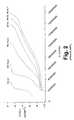
- FIG. 15is a graph showing floating charge versus average programming field for programming voltages applied to a floating gate of a conventional flash device (VP 1 ), a NV floating plate device (VP 2 ), a NV floating device having a gate stack formed with a single injection layer (VP 3 ), and a NV floating device having a gate stack formed with a high K dielectric and a single injection layer (VP 4 ).
- FIG. 16is a graph showing the relationship between the log of the write/erase cycle, or endurance, and the average programming field.
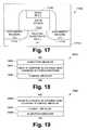
- FIG. 17is one embodiment of a NV floating plate device.
- FIG. 18is one embodiment of a single injector layer gate stack for the NV floating plate device of FIG. 17.
- FIG. 19is one embodiment of a single injector layer gate stack for the NV floating plate device of FIG. 17.
- FIG. 20is one embodiment of the single injector layer gate stack of FIG. 18.
- FIG. 21is one embodiment of the single injector layer gate stack of FIG. 18.
- FIG. 22is one embodiment of a single injector layer gate stack for the NV floating plate device of FIG. 17.
- FIG. 23is one embodiment of a single injector layer gate stack for the NV floating plate device of FIG. 17.
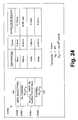
- FIG. 24is one embodiment of the single injector layer gate stack of FIG. 23.
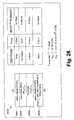
- FIG. 25is one embodiment of a double injector layer gate stack for the NV floating plate device of FIG. 17.
- FIG. 26is one embodiment of the double injector layer gate stack of FIG. 25.
- FIG. 27is one embodiment of a double injector layer gate stack for the NV floating plate device of FIG. 17.
- FIG. 28is one embodiment of the double injector layer gate stack of FIG. 27.
- FIG. 29illustrates a memory device with an array of NV memory cells according to the present invention.
- the present subject matterprovides a scalable Flash/NV structure that further extends the scalability of NV technology by providing a gate stack with a high K dielectric, a charge center or charge storing medium and a least one charge injector medium.
- the insulator stackconsists of either a 4-layer element or a 5-layer element.
- the 4-layer elementprovides a tunneling medium, a charge storing medium, a charge blocking medium and a charge injector medium.
- the 5-layer element stackcreates yet lower field programming by adding a second injector medium.
- the charge store layer and the charge blocking layerare co-produced as one layer, as in the case of SRI, so as to reduce the 4-layer element to a 3-layer element and to reduce the 5-layer element to a 4-layer element.
- the gate stackis programmable with boot-strapped circuits without a charge pump or high voltage add-on technology.
- the gate stackhas an equivalent oxide thickness (t OX ) in the range of 5 nm-15 nm, and a programming voltage across the stack (depending on the stack thickness) as low as 4-5 V, with a programming window of ⁇ 2 V.
- the structure of the present inventionis currently believed to have greater than four orders of magnitude better endurance than possible up until this time. Additionally, the structure of the present invention has variables that are capable of being manipulated to scale the programmable voltages and power. Furthermore, since the programming voltage is significantly less than the breakdown voltage of the dielectric, these variables are capable of being manipulated to achieve faster write-erase cycles. It is believed that the write-erase cycle speed can be enhanced by greater than three orders of magnitude.
- FIG. 1is a graph showing refractive index of silicon-rich silicon nitride films versus SiH 2 Cl 2 /NH 3 flow rate ratio (R). This graph is provided herein to illustrate the known relationship between the silicon amount and the refractive index. The graph indicates that the index of refraction increases linearly with increasing silicon content. As such, the index of refraction of the films can be used as an indication of the silicon content of the films.
- FIG. 2is a graph showing current density versus applied field for silicon-rich silicon nitride films having different percentages of excess silicon.
- the current density (J)is represented in amperes/cm 2
- log Jis plotted against the electric field E (volts/cm) for Si 3 N 4 layers having a SiH 2 Cl 2 /NH 3 flow rate ratio R of 0.1, 3, 5, 10, 15 and 31.
- This graphis provided herein to illustrate the known relationship between the amount of silicon and the conductivity of the film.
- FIG. 3is a graph showing flatband shift versus time at an applied field of 4 ⁇ 10 6 volts/cm for silicon-rich silicon nitride films having varying percentages of excess silicon.
- R3
- the flatband shiftis greater than the shifts produced by films having an R of 0.1, 10 or 15.
- the film having an R of 10provides a greater flatband shift than a film having an R of 15.
- FIGS. 3 and 4are provided to illustrate the characteristics of a charge storing medium and a more conductive charge injector medium as further explained below.
- Silicon-rich silicon nitride films deposited at an R of 3 or 5will possess a charge storing function or property normally provided by a polysilicon floating gate of a EEPROM cell.
- silicon-rich nitride films having an R greater than 0.1 and less than 10(or, more specifically, having an index of refraction between approximately 2.10 and 2.30) will provide appreciably enhanced charge trapping or charge storing properties without providing appreciably enhanced charge conduction. This charge trapping is characteristic of a charge storing medium that can be used as a floating plate within a gate stack of a NV device.
- Silicon-rich nitride films having an R greater than 10are referred to as an injector medium.
- Silicon nitride injectorsare preferred over silicon oxide injectors because the two-phase nature of the interface is believed to provide a localized electric field distortion and an associated enhanced charge transport (high conduction). Silicon readily diffuses within silicon oxide at elevated processing temperatures, which disrupts the injection threshold by reducing the localized field distortions. However, even at higher processing temperature, silicon does not readily diffuse with Si 3 N 4 .
- FIG. 5is a graph showing apparent dielectric constant K versus refractive index for both Silicon Rich Nitride (SRN) and Silicon Rich Oxide (SRO).
- SRNSilicon Rich Nitride
- SROSilicon Rich Oxide
- the SRO and SRO plotted in this graphwere provided using a Low Pressure Chemical Vapor Deposition (LPCVD) process.
- the SROwas fabricated at approximately 680° C., and the fabricated structure included 100 ⁇ oxide and 150 ⁇ SRO.
- the SRNwas fabricated at approximately 770° C., and the fabricated structure included 45 ⁇ oxide and 80 ⁇ SRN.
- the dielectric constant of siliconis around 12. Materials with a higher K than silicon are conventionally termed a high K material, and materials with a lower K than silicon are conventionally termed a low K material.
- Injector SRIincludes these high K SRO and high K SRN.
- Charge-centered SRIincludes low K SRO and low K SRN.
- FIG. 6is a cross-section view of a conventional nonvolatile field effect transistor (NV FET) device such as a Flash device.
- the illustrated deviceis fabricated on a silicon substrate 612 such as a p silicon substrate or p-well in which case it is referred to as a source electrode (SE), and is separated from other devices by the isolation trenches 614 .
- the device 610further includes diffused regions that function as a drain region 616 and a source region 618 , such as the illustrated n+ diffused regions in the p substrate.
- a field effect transistor (FET) channel 620is formed in the substrate between the drain and source regions.
- FETfield effect transistor
- a source contact 622is formed to electrically couple with the source region 618
- a bit contact 624is formed to electrically couple with the drain region 616 .
- a floating polysilicon gate 626is formed over the FET channel 620 , and is separated from the FET channel 620 by tunnel oxide 628 .
- a control gate 630referred to as a program electrode (PE) for the illustrated embodiment, is formed over the floating polysilicon gate 626 .
- An oxide/nitride/oxide (ONO) interpoly dielectric 632is provided around and between the PE 630 and the floating gate 626 .
- a bit lineis connected to the bit contact, and a word line is connected the PE.
- An oxide 633is formed around the NV FET device.
- the cell size for a NAND gateis approximately 0.15 ⁇ m 2 .
- the FET channelis approximately 150 nm wide.
- Both the floating gate and the PEare approximately 150 nm wide and about 250 nm thick.
- the tunnel oxide separating the floating gate from the FET channelis approximately 8 nm thick.
- the ONO interpoly dielectric separating the PE and the floating gateis approximately 15 nm thick.
- the programming voltage applied to the PEis about 16 volts, and the pulse width of a programming pulse is approximately 1 ms.
- the field generated across the tunnel oxideis approximately 12 ⁇ 10 6 V/cm.
- the minimum program window(V T (“1”) ⁇ V T (“0”)) is approximately 2 V.
- the minimum program windowis defined as the difference in the threshold voltages for a device with a stored one and a device with a stored zero.
- the endurance for a typical NV FET deviceis about 10 5 write/erase cycles.
- the power supply V DDis 3.3 V.
- FIG. 7illustrates the capacitive coupling for a conventional Flash device.
- the device 710includes a control gate or PE 730 , a floating gate 726 , and a substrate or SE 712 .
- a programming voltage VP 1 of 16 Vis applied to the control gate.
- the electric field across about 8 nm of tunnel oxide 728 (E TUN.OX )is approximately 12 ⁇ 10 6 V/cm, which reflects a coupling efficiency of about 60%. The low efficiency is attributable to the geometry and capacitor divider effects of the cell.
- FIG. 8illustrates the capacitive coupling for a nonvolatile floating plate device.
- the device 840includes a control gate 830 separated from a substrate by a gate stack 842 .
- the gate stack 842includes a tunnel insulator 844 , charge centers 846 that form a floating plate capable of storing charge, and a charge blocking dielectric 848 .
- a programming voltage VP 2 of 9.2 Vis applied to the control gate 830 .
- the average electric field E AVG between the charge centers 846 and the substrate 812is between about 6 to 7 ⁇ 10 6 V/cm.
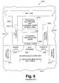
- FIG. 9illustrates the average field enhancement due to the incorporation of a top injection layer in a gate stack for a nonvolatile floating plate device.
- the gate stack 940which is interposed between the control gate 930 and the substrate 912 , includes a tunnel layer 950 , a charge blocking layer 952 that includes charge centers 946 that form a floating plate or a charge storing medium, and an injector layer 954 .
- the gate stack dielectricis SiO 2 , which has a dielectric constant of about 4.
- the injector layer 954enhances the electric field by a factor of about 1.5 (1.5 ⁇ ).
- a programming voltage VP 3 of 5.5 to 6.5 Vis applied to the control gate 930 .
- the resulting average electric field E AVG between the charge centers 946 and the substrate 912is reduced to about 4 ⁇ 10 6 V/cm.
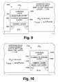
- FIG. 10illustrates the average field enhancement due to the incorporation of a bottom injection layer in a gate stack for a nonvolatile floating plate device.
- the gate stack 1040which is interposed between the control gate 1030 and the substrate 1012 , includes an injector layer 1056 , a tunnel layer 1050 , and a charge blocking layer 1052 that includes charge centers 1046 that form a floating plate or a charge storing medium.
- the gate stack dielectricis SiO 2 .
- a programming voltage VP 3 of 5.5 to 6.5 Vis applied to the control gate 1030 .
- the resulting average electric field E AVG between the charge centers 1046 and the substrate 1012is reduced to about 4 ⁇ 10 6 V/cm. This illustrates that the same general results are achieved whether the injector layer is on top of the gate stack or on the bottom of the gate stack. That is, the injector layer enhances the electric field by a factor of about 1.5
- FIG. 11illustrates the average field enhancement due to the incorporation of both a top injection layer and a bottom injection layer in a gate stack for a nonvolatile floating plate device.
- the gate stack 1140which is interposed between the control gate 1130 and the substrate 1112 , includes a first injector layer 1156 , a tunnel layer 1150 , a charge blocking layer 1152 that includes charge centers 1146 that form a floating plate or a charge storing medium, and a second injector layer 1154 .
- the gate stack dielectricis SiO 2 .
- the use of an injector layer on the top and on the bottom of the gate stackenhances the electric field by a factor of about 1.7 (1.7 ⁇ ).
- a programming voltage VP 3 of 5.5 to 6.5 Vis applied to the control gate 1130 .
- the resulting average electric field E AVG between the charge centers 1146 and the substrate 1112is reduced to about 3.5 ⁇ 10 6 V/cm.
- the illustrationsshow a high K dielectric is used as the base dielectric for both the charge blocking layer and the tunnel layer.
- the high K dielectricallows the device to be scaled to smaller sizes and allows smaller electric fields and programing voltages to be applied.
- FIG. 12illustrates the average field enhancement due to the incorporation of a high K dielectric and a top injection layer in a gate stack for a nonvolatile floating plate device.
- the average field enhancement due to the Al 2 O 3is approximately 1.6 greater than that for the illustration of FIG. 9 that used SiO 2 as the gate dielectric; i.e. the average field enhancement is approximately 1.6 of 1.5 ⁇ .
- a programming voltage VP 4 of 3.5 to 4 Vis applied to the control gate 1230 .
- the resulting average electric field E AVG between the charge centers 1246 and the substrate 1212is, therefore, reduced to about 2.5 ⁇ 10 6 V/cm.
- FIG. 13illustrates the average field enhancement due to the incorporation of a high K dielectric and a bottom injection layer in a gate stack for a nonvolatile floating plate device.
- the average field enhancement due to the Al 2 O 3is approximately 1.6 times greater than that for the illustration of FIG. 10 that used SiO 2 as the gate dielectric; i.e. the average field enhancement is approximately 1.6 of 1.5 ⁇ .
- a programming voltage VP 4 of 3.5 to 4 Vis applied to the control gate 1330 .
- the resulting average electric field E AVG between the charge centers 1346 and the substrate 1312is reduced to about 2.5 ⁇ 10 6 V/cm.
- FIG. 14illustrates the average field enhancement due to the incorporation of a high K dielectric and both a top injection layer and a bottom injection layer in a gate stack for a nonvolatile floating plate device.
- the average field enhancement due to the Al 2 O 3is approximately 1.6 times greater than that for the illustration of FIG. 11 that used SiO 2 as the gate dielectric; i.e. the average field enhancement is approximately 1.6 of 1.7 ⁇ .
- a programming voltage VP 4 of 3.5 to 4 Vis applied to the control gate 1430 .
- the resulting average electric field E AVG between the charge centers 1446 and the substrate 1412is reduced to about 2.2 ⁇ 10 6 V/cm.
- FIG. 15is a graph showing floating charge versus average programming field for programming voltages applied to a floating gate of a conventional flash device (VP 1 ), a NV floating plate device (VP 2 ), a NV floating device having a gate stack formed with a single injection layer (VP 3 ), and a NV floating device having a gate stack formed with a high K dielectric and a single injection layer (VP 4 ).
- the graphillustrates that a larger electric field is required to store a desired charge on a floating gate rather than on one of the floating plates. Reducing the required average programming field reduces the required programming voltage, which allows the NV device to be scaled with the other devices. Additionally, reducing the required programming voltage provides a margin with respect to the breakdown of the dielectric. A higher than required programming voltage can be applied to provide a quicker write or erase. Furthermore, for a generic write or erase speed, such reduction in programming voltage enhances endurance; i.e. the number of write/erase cycles.
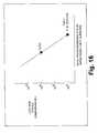
- FIG. 16is a graph showing the relationship between the log of the write/erase cycle, or endurance, and the average programming field.
- the graphillustrates a linear relationship between the average programming field and endurance such that reducing the average programming field in half increases the endurance by almost four orders of magnitude, and reducing the average programming field to one fourth of an original field increases the endurance by almost eight orders of magnitude, i.e. by a factor of 100,000,000.
- FIG. 17is one embodiment of a NV floating plate device.
- the device 1740includes a gate stack 1742 that is formed on a p-type silicon substrate 1712 between two n-type diffusion regions 1716 and 1718 in the substrate.
- a gate 1730is formed on the gate stack 1742 .
- the diffusion regions in the illustrated embodimentare n+ diffusion regions, and the substrate is a p substrate.
- the substratefunctions as a source electrode (S.E.) and the gate functions as a programming electrode (P.E.).
- S.E.source electrode
- P.E.programming electrode
- the gatemay be either a doped polysilicon gate such as a n+ or p+ diffused silicon, or may be a metal gate. Examples of a metal gate include TiN and WSi.
- CMOS technologycould either be bulk CMOS or SOI CMOS technology.
- FIG. 18is one embodiment of a single injector layer gate stack or single electron injector structure (SEIS) for the NV floating plate device of FIG. 17.
- the gate stack 1842includes a tunnel medium 1850 , a combination high K charge blocking and charge storing medium 1860 , and an injector medium 1854 .
- the injector medium 1854provides charge transfer through enhanced tunneling.
- the term charge storing mediumconnotes a medium that has charge centers that provide a charge trapping property.
- the combination high K charge blocking and charge storing medium 1860includes nano crystals dispersed into a high K dielectric either through doping or implantation.
- FIG. 19is one embodiment of a single injector layer gate stack or single electron injector structure (SEIS) for the NV floating plate device of FIG. 17.
- SEISsingle electron injector structure
- the gate stack 1942includes an injector medium 1956 , a tunnel medium 1950 , and a combination high K charge blocking and charge storing medium 1960 .
- the injector mediummay be used either as the top layer (near the program electrode) or as the bottom layer (near the source electrode) of the gate structure.
- the combination high K charge blocking and charge storing medium 1960includes nano crystals dispersed into a high K dielectric either through doping or implantation.
- FIG. 20is one embodiment of the single injector layer gate stack or single electron injector structure (SEIS) of FIG. 18.
- the gate stack 2042includes an Al 2 O 3 tunnel medium 2050 , silicon-rich Al 2 O 3 2060 functioning as the combination high K charge blocking and charge storing medium, and an SRN injector medium 2054 .
- Silicon-rich Al 2 O 3 2060includes dispersed silicon nano crystals to provide the medium with a refractive index sufficient to provide charge centers that trap or store charge.
- the thickness of the tunnel Al 2 O 3is 6 nm which corresponds to a t OX equivalent of about 2.5 nm
- the thickness of the silicon-rich Al 2 O 3is 10 to 12 nm which corresponds to a t OX equivalent of about 5 nm
- the thickness of the injector SRNis 5 nm which corresponds to a t OX equivalent of about 1.5 nm.
- the total equivalent oxide thickness (t OX.EQ.TOTAL )is approximately 9 nm.
- a programming voltage (V P ) of 3.6 Vprovides an effective programming field (E P ) of about 4 ⁇ 10 6 V/cm. A number of variables may be manipulated.
- An effective range for the Al 2 O 3 tunnel mediumis 3 to 10 nm, for the silicon-rich Al 2 O 3 is 6 to 30 nm, and for the SRN injector medium is 3 to 10 nm.
- One of ordinary skill in the artwill understand, upon reading and understanding this disclosure, how to manipulate these variables to achieve the desired characteristics for the gate stack.
- FIG. 21is one embodiment of the single injector layer gate stack of FIG. 18.
- the gate stack 2142includes a SiO 2 tunnel medium 2150 , silicon rich Al 2 O 3 2160 functioning as the combination high K charge blocking and charge storing medium, and an SRN injector medium 2154 .
- the thickness of the tunnel SiO 2is 5 nm which corresponds to a t OX of about 5 nm
- the thickness of the silicon-rich Al 2 O 3is 10 to 12 nm which corresponds to a t OX equivalent of about 5 nm
- the thickness of the injector SRNis 5 nm which corresponds to a t OX equivalent of about 1.5 nm.
- the total equivalent oxide thickness (t OX.EQ.TOTAL )is approximately 11.5 nm.
- a programming voltage (V P ) of 4.6 Vprovides an effective programming field (E P ) of about 4 ⁇ 10 6 V/cm. A number of variables may be manipulated.
- An effective range for the SiO 2 tunnel mediumis 4 to 8 nm, for the silicon-rich Al 2 O 3 is 6 to 30 nm, and for the SRN injector medium is 3 to 10 nm.
- One of ordinary skill in the artwill understand, upon reading and understanding this disclosure, how to manipulate these variables to achieve the desired characteristics for the gate stack.
- FIG. 22is one embodiment of a single injector layer gate stack or single electron injector structure (SEIS) for the NV floating plate device of FIG. 17.
- the gate stack 2242includes a tunnel medium 2250 , a charge storing medium 2264 with nano crystals, a high K charge blocking medium 2262 , and an injector medium 2254 .
- the nano crystals in the charge storing mediumare disposed in a high K dielectric either through doping or implantation.
- FIG. 23is one embodiment of a single injector layer gate stack or single electron injector structure (SEIS) for the NV floating plate device of FIG. 17.
- SEISsingle electron injector structure
- the gate stack 2342includes an injector medium 2356 , a tunnel medium 2350 , a charge storing medium 2364 with nano crystals, and a high K charge blocking medium 2362 .
- the nano crystals in the charge storing mediumare disposed in a high K dielectric either through doping or implantation.
- FIG. 24is one embodiment of the single injector layer gate stack of FIG. 22.
- the gate stack 2442includes an Al 2 O 3 tunnel medium 2450 , Al 2 O 3 with silicon nano crystals 2464 functioning as a charge storing medium, Al 2 O 3 2462 functioning as a high K charge blocking medium, and an SRN injector medium 2454 .
- the thickness of the tunnel Al 2 O 3is 5 nm which corresponds to a t OX equivalent of about 2.5 nm
- the thickness of the Al 2 O 3 with silicon nano crystalsis 4 nm which corresponds to a t OX equivalent of about 1.6 nm
- the thickness of the blocking Al 2 O 3is 10 nm which corresponds to a t OX equivalent of about 4.5 nm
- the thickness of the injector SRNis 5 nm which corresponds to a t OX equivalent of about 1.5 nm.
- the total equivalent oxide thickness (t OX EQ.TOTAL )is approximately 10 nm.
- a programming voltage (V P ) of 4 Vprovides an effective programming field (E P ) of about 4 ⁇ 10 6 V/cm.
- E Peffective programming field
- An effective range for the Al 2 O 3 tunnel mediumis 5 to 8 nm, for the Al 2 O 3 with silicon nano crystals is 3 to 5 nm, for the blocking Al 2 O 3 is 6 to 30 nm, and for the SRN injector medium is 3 to 10 nm.
- One of ordinary skill in the artwill understand, upon reading and understanding this disclosure, how to manipulate these variables to achieve the desired characteristics for the gate stack.
- FIG. 25is one embodiment of a double injector layer gate stack or double electron injector structure (DEIS) for the NV floating plate device of FIG. 17.
- the gate stack 2542includes an injector medium 2556 , a tunnel medium 2550 , a combination charge blocking and storing medium 2560 , and an injector medium 2554 .
- the use of two injector layersprovides further field enhancements as provided above.
- FIG. 26is one embodiment of the double injector layer gate stack of FIG. 25.
- the gate stack 2642includes an SRN injector medium 2656 , an Al 2 O 3 tunnel medium 2650 , silicon rich Al 2 O 3 2660 functioning as the combination high K charge blocking and charge storing medium, and an SRN injector medium 2654 .
- the thickness of the first injector SRN that is deposited “NH 3 ” or “NO” surface treated substrateis 5 nm which corresponds to a t OX equivalent of about 2.5 nm
- the thickness of the tunnel Al 2 O 3is 5 to 6 nm which corresponds to a t OX equivalent of about 2.5 nm
- the thickness of the silicon-rich Al 2 O 3is 10 to 12 nm which corresponds to a t OX equivalent of about 5 nm
- the thickness of the second injector SRNis 5 nm which corresponds to a t OX equivalent of about 1.5 nm.
- the total equivalent oxide thickness (t OX.EQ.TOTAL )is approximately 11.5 nm.
- a programming voltage (V P ) of 3 to 3.3 Vprovides an effective programming field (E P ) of about 2.6 to 3.0 ⁇ 10 6 V/cm.
- E Peffective programming field
- An effective range for the first SRN injector mediais 3 to 10 nm, for the Al 2 O 3 tunnel medium is 5 to 8 nm, for the silicon-rich Al 2 O 3 is 6 to 30 nm, and for the second SRN injector medium is 3 to 10 nm.
- One of ordinary skill in the artwill understand, upon reading and understanding this disclosure, how to manipulate these variables to achieve the desired characteristics for the gate stack.
- FIG. 27is one embodiment of a double injector layer gate stack or double electron injector structure (DEIS) for the NV floating plate device of FIG. 17.
- the gate stack 2742includes an injector medium 2756 , a tunnel medium 2750 , a charge storing medium 2764 , a charge blocking medium 2762 , and an injector medium 2754 .
- FIG. 28is one embodiment of the double injector layer gate stack of FIG. 27.
- the gate stack 2842includes an SRN injector medium 2856 , an Al 2 O 3 tunnel medium 2850 , Al 2 O 3 with silicon nano crystals 2864 functioning as a charge storing medium, Al 2 O 3 functioning as a charge blocking medium 2862 , and an SRN injector medium 2854 .
- the thickness of the first injector SRN that is deposited “NH 3 ” or “NO” surface treated substrateis 5 nm which corresponds to a t OX equivalent of about 2.5 nm
- the thickness of the tunnel Al 2 O 3is 5 to 6 nm which corresponds to a t OX equivalent of about 2.5 nm
- the thickness of the Al 2 O 3 with silicon nano crystalsis 4 nm which corresponds to a t OX equivalent of about 1.6 nm
- the thickness of the blocking Al 2 O 3is 10 nm which corresponds to a t OX equivalent of about 4.5 nm
- the thickness of the injector SRNis 5 nm which corresponds to a t OX equivalent of about 1.5 nm.
- the total equivalent oxide thickness (t OX.EQ.TOTAL )is approximately 12.6 nm.
- a programming voltage (V P ) of 3.25 Vprovides an effective programming field (E P ) of about 2.6 ⁇ 10 6 V/cm.
- V Pprogramming voltage
- E Peffective programming field
- An effective range for the first SRN injector mediumis 3 to 10 nm, for the Al 2 O 3 tunnel medium is 5 to 8 nm, for the Al 2 O 3 with silicon nano crystals is 3 to 5 nm, for the blocking Al 2 O 3 is 6 to 30 nm, and for the second SRN injector medium is 3 to 10 nm.
- One of ordinary skill in the artwill understand, upon reading and understanding this disclosure, how to manipulate these variables to achieve the desired characteristics for the gate stack.
- Injector SRNwas provided as an example of an injector medium in the above examples.
- materialsinclude silicon-rich aluminum nitride and SRO.
- Al 2 O 3is not an effective diffusion barrier for certain dopants like phosphorus for an n+ gate.
- the injector media SRN and silicon-rich aluminum nitridefunction as a diffusion barrier for doped polysilicon gates to prevent phosphorous, for example, from diffusing into Al 2 O 3 .
- a diffusion barrieris not needed if a metal gate is used.
- injector SRNWhen injector SRN is deposited over a silicon substrate, the substrate is “NO” or “NH 3 ” surface treated to reduce the interface states density and leakage at the silicon substrate. This surface treatment adds 1 nm to the equivalent of additional oxide thickness (t OX.EQ ) of the injector SRN.
- This thicker t OX equivalentis illustrated in FIG. 25, where the top injector SRN has a t OX equivalent of 1.5 nm and the bottom injector SRN deposited over “NO” or “NH 3 ” surface treated substrate has a t OX equivalent of 2.5 nm.
- a high K charge blocking mediumis a material that has a K greater than the K of silicon. These materials include oxides, nitrides and silicates of Tantalum, Titanium, Zirconium, Hafnium and Praseodymium.
- these materialsmay further be doped with complex high K dielectrics such as barium strontium titanate (BST), transition metal, and metal oxides such as tantalum pentoxide (Ta 2 O 5 ), titanium dioxide (TiO 2 ), tantalum nitride (TaN), zirconium oxide (ZrO 2 ), and praseodymium oxide (Pr 2 O 3 ).
- BSTbarium strontium titanate
- transition metaland metal oxides such as tantalum pentoxide (Ta 2 O 5 ), titanium dioxide (TiO 2 ), tantalum nitride (TaN), zirconium oxide (ZrO 2 ), and praseodymium oxide (Pr 2 O 3 ).
- Silicon rich Al 2 O 3was provided as an example of a combination high K charge blocking and charge storing medium in the above examples.
- materialsinclude any of the high K charge blocking media provided above with nano crystals dispersed through the media.
- Various embodimentsinclude a high K charge blocking media with silicon nano crystals, gold nano crystals, tungsten nano crystals, and/or silicided tungsten nano crystals.
- the nano crystalswere dispersed into a high K dielectric either through doping or implantation.
- the nano crystalsmay be distributed using a number of techniques, including simultaneous sputtering, implantation, chemical vapor deposition, atomic layer deposition (ALD) and molecular beam epitaxy (MBE).
- Al 2 O 3 and SiO 2were provided as examples of a tunnel medium in the above examples. These materials may be interchanged with each other. Al 2 O 3 has a higher dielectric constant, whereas SiO 2 is easier to fabricate.
- FIG. 29illustrates a memory device with an array of NV memory cells according to the present invention.
- the memory device 2970includes an array 2972 of NV memory cells as described above.
- a grid of row conductors 2974 and column conductors 2976are used to selectively write/erase a memory cell 2978 .
- the memory device 2970includes power circuitry 2980 , row select circuitry 2982 and column select circuitry 2984 .
- the row select circuitry and column select circuitrycooperate with each other to select a memory cell to be written or erased using power provided by the power circuitry.
- Input/output circuitry and padsnot shown, defines the inputs and outputs of such device.
- the memory deviceis used in a number of nonvolatile multi-threshold FET devices such as PROM, FLASH, EPROM, EEPROM, and antifuse devices.
- Such an electronic systemincludes a processor or arithmetic/logic unit (ALU), a control unit, a memory device unit and an input/output (I/O) device.
- ALUarithmetic/logic unit
- control unita control unit
- memory device unita memory device unit
- I/Oinput/output
- Such an electronic systemwill have a native set of instructions that specify operations to be performed on data by the processor and other interactions between te processor, the memory device unit and the I/O devices.
- the memory device unitcontains the data plus a stored list of instructions.
- the control unitcoordinates all operations of the processor, the memory device and the I/O devices by continuously cycling through a set of operations that cause instructions to be fetched from the memory device and executed.
- NV memory device and arraysare coupled to input/output nodes of the rand-logic device or PLA as appropriate for the desired function
- the present subject matterprovides a gate stack for a nonvolatile multi-threshold FET device that promotes low power, low programming voltage for write and erase cycles, and improved endurance.
- a higher capacitive coupling efficiencyis achieved by replacing floating gate technology with floating plate (charge center) technology, and using a high K dielectric.
- an injector mediumenhances the tunneling effect.
- the gate stackis capable of being used in applications which are compatible and scalable with power supply and lithography scaling. Additionally, the gate stack is capable of being used in devices and circuits that readily integrate with general fixed threshold memory and logic devices, circuits and functions. Due the lower programming voltage and electric field, which is considerably less than the breakdown of the dielectric, the gate stack promotes faster writing and erasing capabilities.
Landscapes
- Engineering & Computer Science (AREA)
- Microelectronics & Electronic Packaging (AREA)
- Chemical & Material Sciences (AREA)
- Physics & Mathematics (AREA)
- Nanotechnology (AREA)
- Crystallography & Structural Chemistry (AREA)
- General Physics & Mathematics (AREA)
- Condensed Matter Physics & Semiconductors (AREA)
- General Chemical & Material Sciences (AREA)
- Manufacturing & Machinery (AREA)
- Computer Hardware Design (AREA)
- Power Engineering (AREA)
- Mathematical Physics (AREA)
- Theoretical Computer Science (AREA)
- Chemical Kinetics & Catalysis (AREA)
- Non-Volatile Memory (AREA)
- Semiconductor Memories (AREA)
Abstract
Description
- This invention relates generally to integrated circuits and, more particularly, to nonvolatile programmable memory cells and reprogrammable logic circuit elements.[0001]
- General CMOS silicon gate technology has been scaled rapidly from the 1.0 μm generation (V[0002]DD=5.0 V) to the 0.13 μm generation (VDD=1.5 V) over a period of little over a decade. However, the progress of scaling Flash/NV programming voltage and power has been limited. Additionally, the Flash/NV devices have a limited endurance. That is, these devices are capable of performing a limited number of write/erase cycles that prevent their use in a number of applications. The progress of extending the endurance of Flash/NV devices also has been limited.
- Most NV devices have a floating gate and use a power hungry channel hot electron write process and a tunnel erase process through the tunnel oxide. The tunnel erase process requires both a high programming voltage and a programming field that approaches the breakdown of the oxide. Thus, conventional Flash/NV devices require attributes of high voltage technology and circuitry in an environment of scaled low voltage CMOS technology. As such, the integration of NV devices with general high performance logic technology and DRAM technology is complicated. Additionally, the endurance of these NV devices is limited to about 10E5-10E6 cycles. Therefore, providing embedded Flash/EPROM in a general random logic or DRAM environment to achieve enriched functions requires complex circuitry and many additional masks, resulting in a relatively limited yield and high cost.[0003]
- Two phase insulating materials, referred to as silicon-rich insulators (SRI), are known. SRI includes controlled and fine dispersions of crystalline silicon in a background of stoichiometric insulator such as SiO[0004]2(referred to as silicon-rich oxide or SRO), or Si3N4(referred to as silicon-rich nitride or SRN). A unique set of insulators with a controlled and wide range of electrical properties can be formed by controlling the amount, distribution and size of silicon crystals.
- SRI materials are capable of possessing charge trapping and charge injecting properties. “Charge-centered” SRI has refractive index in a range that provides the material with the property for trapping electrons or holes at the silicon centers due to the creation of quantum potential wells. “Injector” SRI has a refractive index in a range that provides the material with silicon centers that are within tunneling distance of each other such that charge can readily communicate between the charge centers. Injector SRI is characterized by high conductivity and behaves like semi-metal. The apparent high frequency dielectric constant of this material is greater than that of silicon. When superimposed on top of a dielectric, charge injected into this material from a metal plate is uniformly distributed to the silicon centers, which in turn injects charges uniformly into the insulator when biased. Thus, the injector SRI reduces local field fluctuations due to defects. At the same time, a large number of silicon injector centers at the insulator interface provides a geometrical pattern that enhances the tunneling, and thus the charge transfer or conduction, at significantly reduced average fields. This material has been termed an “injector” because of this enhanced tunneling.[0005]
- Charge-centered or trapping SRI is a charge storing medium that includes charge-centered SRO characterized by a refractive index in the approximate range of 1.5 to 1.6, and further includes charge-centered SRN characterized by a refractive index in the approximate range from 2.1 to 2.2. Injector SRI is a charge injector medium that includes injector SRO characterized by a refractive index that is approximately 1.85 and greater, and further includes injector SRN characterized by a refractive index that is approximately 2.5 and greater. It was observed that the SRN class of materials was significantly more stable at high temperature compared to SRO in terms of interdiffusion and growth of silicon centers during high temperature processing as well as in terms of providing a reproducible interface between silicon and SRI and/or SiO[0006]2and SRI.
- It has been proposed to use charge centered and injector SRI material in a variety of NV FET structures and associated Flash, PROM, EPROM, EEPROM, antifuse cells and arrays. In one of these proposed embodiments, the gate insulator stack includes a tunnel oxide, a thin layer of charge-centered SRN to trap charges and thereby act like a “floating plate,” an overlayer of thicker CVD oxide, and a layer of injector SRN. The top CVD oxide is designed to prevent charge loss at the operating field and to be optimized for the appropriate programming voltage. The equivalent oxide thickness (t[0007]ox) of the gate insulator stack is primarily dependent on the tunnel oxide and the barrier CVD oxide thickness. The stack is scalable with respect to the programming voltage because the required programming field is reduced to 6-7E6 V/cm due to the injector-induced enhanced tunneling compared to 10-11E6 V/cm for a conventional NV/FET structure. Additionally, the programming gate voltage is directly coupled into the charge-centered layer to provide 100% coupling efficiency compared to the typical floating gate structures where capacitor divider effects and the cell geometry determine the coupling efficiency. The coupling efficiency for a floating gate structure is typically around 50%-70%. These proposed devices were shown to exhibit many orders of magnitude greater retention because of the reduced programming field. These devices are significantly more power efficient as they are written to and erased by direct tunneling, rather than by channel hot electron injection. However, the write/erase fields were still too high, and both the endurance and power reductions were still too limited.
- Silicon “quantum dots” of 3 nm to 10 nm diameter have been fabricated in a controlled manner by either Low Pressure Chemical Vapor Deposition (LPCVD) followed by oxidation or by gas phase pyrolysis of silane to create nano crystal silicon aerosol. It has been proposed to either place these silicon nano crystals on top of the tunnel oxide or embed them into the gate insulator oxide. These nano crystals behave as charge centers similar to the charge-centered SRI layer described above. NV FET gate stacks were formed with the silicon quantum dots by adding a thicker oxide overlayer. While somewhat reduced voltage write/erase and up to 10E6 endurance were demonstrated, the write/erase fields were still too high, and both the endurance and the power reductions were still too limited.[0008]
- Therefore, there is a need in the art to provide Flash/NV technology that overcomes these problems by being capable of using scalable programmable voltages and power, by being easily integratable with general scaled logic technology while minimizing the overhead associated with Flash/NV technology features, by extending endurance, and by providing faster write-erase cycles without impacting retention and reliability.[0009]
- The above mentioned problems are addressed by the present subject matter and will be understood by reading and studying the following specification. The present subject matter provides a scalable Flash/NV structure that further extends the scalability of NV technology by providing a gate stack with a high K dielectric, a charge center or charge storing medium and at least one charge injector medium. The present subject matter requires a lower programming field, improves endurance, achieves faster write-erase cycles, and has variables that are capable of being manipulated for scaling purposes.[0010]
- One aspect is a gate stack for a nonvolatile device. According to one embodiment, the gate stack includes a tunnel medium, a high K charge blocking and charge storing medium, and an injector medium. According to this embodiment, the high K charge blocking and charge storing medium is disposed on the tunnel medium. Also according to this embodiment, the injector medium is operably disposed with respect to the tunnel medium and the high K charge blocking and charge storing medium to provide charge transport by enhanced tunneling. According to one embodiment, the injector medium is disposed on the high K charge blocking and charge storing medium. According to one embodiment, the tunnel medium is disposed on the injector medium.[0011]
- One embodiment of the gate stack includes a first injector medium, a tunnel medium disposed on the first injector medium, a high K charge blocking and charge storing medium disposed on the tunnel medium, and a second injector medium disposed on the high K charge blocking and charge storing medium.[0012]
- According to one embodiment, the gate stack includes a tunnel medium, a high K charge storing medium disposed on the tunnel medium, a high K charge blocking medium stored on the high K charge storing medium, and an injector medium. The injector medium is operably disposed with respect to the tunnel medium, the high K charge storing medium and the high K charge blocking medium to provide charge transport by enhanced tunneling. According to one embodiment, the injector medium is disposed on the high K charge blocking and charge storing medium. According to one embodiment, the tunnel medium is disposed on the injector medium.[0013]
- One embodiment of the gate stack includes a first injector medium disposed on a substrate, a tunnel medium disposed on the first injector medium, a high K charge storing medium disposed on the tunnel medium, a high K charge blocking medium stored on the high K charge storing medium, and a second injector medium disposed on the high K charge blocking medium.[0014]
- These and other aspects, embodiments, advantages, and features will become apparent from the following description of the invention and the referenced drawings.[0015]
- FIG. 1 is a graph showing refractive index of silicon-rich silicon nitride films versus SiH[0016]2Cl2/NH3flow rate ratio.
- FIG. 2 is a graph showing current density versus applied field for silicon-rich silicon nitride films having different percentages of excess silicon.[0017]
- FIG. 3 is a graph showing flat band shift versus time at an applied field of 4×10[0018]6volts/cm for silicon-rich silicon nitride films having varying percentages of excess silicon.
- FIG. 4 is a graph showing flat band shift versus time at an applied field of 7×10[0019]6volts/cm for silicon-rich silicon nitride films having varying percentages of excess silicon.
- FIG. 5 is a graph showing apparent dielectric constant K versus refractive index for both Silicon Rich Nitride (SRN) and Silicon Rich Oxide (SRO).[0020]
- FIG. 6 is a cross-section view of a conventional nonvolatile field effect transistor (NV FET) device or Flash device.[0021]
- FIG. 7 illustrates the capacitive coupling for a conventional Flash device.[0022]
- FIG. 8 illustrates the capacitive coupling for a nonvolatile floating plate device.[0023]
- FIG. 9 illustrates the average field enhancement due to the incorporation of a top injection layer in a gate stack for a nonvolatile floating plate device.[0024]
- FIG. 10 illustrates the average field enhancement due to the incorporation of a bottom injection layer in a gate stack for a nonvolatile floating plate device.[0025]
- FIG. 11 illustrates the average field enhancement due to the incorporation of both a top injection layer and a bottom injection layer in a gate stack for a nonvolatile floating plate device.[0026]
- FIG. 12 illustrates the average field enhancement due to the incorporation of a high K dielectric and a top injection layer in a gate stack for a nonvolatile floating plate device.[0027]
- FIG. 13 illustrates the average field enhancement due to the incorporation of a high K dielectric and a bottom injection layer in a gate stack for a nonvolatile floating plate device.[0028]
- FIG. 14 illustrates the average field enhancement due to the incorporation of a high K dielectric and both a top injection layer and a bottom injection layer in a gate stack for a nonvolatile floating plate device.[0029]
- FIG. 15 is a graph showing floating charge versus average programming field for programming voltages applied to a floating gate of a conventional flash device (VP[0030]1), a NV floating plate device (VP2), a NV floating device having a gate stack formed with a single injection layer (VP3), and a NV floating device having a gate stack formed with a high K dielectric and a single injection layer (VP4).
- FIG. 16 is a graph showing the relationship between the log of the write/erase cycle, or endurance, and the average programming field.[0031]
- FIG. 17 is one embodiment of a NV floating plate device.[0032]
- FIG. 18 is one embodiment of a single injector layer gate stack for the NV floating plate device of FIG. 17.[0033]
- FIG. 19 is one embodiment of a single injector layer gate stack for the NV floating plate device of FIG. 17.[0034]
- FIG. 20 is one embodiment of the single injector layer gate stack of FIG. 18.[0035]
- FIG. 21 is one embodiment of the single injector layer gate stack of FIG. 18.[0036]
- FIG. 22 is one embodiment of a single injector layer gate stack for the NV floating plate device of FIG. 17.[0037]
- FIG. 23 is one embodiment of a single injector layer gate stack for the NV floating plate device of FIG. 17.[0038]
- FIG. 24 is one embodiment of the single injector layer gate stack of FIG. 23.[0039]
- FIG. 25 is one embodiment of a double injector layer gate stack for the NV floating plate device of FIG. 17.[0040]
- FIG. 26 is one embodiment of the double injector layer gate stack of FIG. 25.[0041]
- FIG. 27 is one embodiment of a double injector layer gate stack for the NV floating plate device of FIG. 17.[0042]
- FIG. 28 is one embodiment of the double injector layer gate stack of FIG. 27.[0043]
- FIG. 29 illustrates a memory device with an array of NV memory cells according to the present invention.[0044]
- The following detailed description of the invention refers to the accompanying drawings which show, by way of illustration, specific aspects and embodiments in which the invention may be practiced. In the drawings, like numerals describe substantially similar components throughout the several views. These embodiments are described in sufficient detail to enable those skilled in the art to practice the invention. Other embodiments may be utilized and structural, logical, and electrical changes may be made without departing from the scope of the present invention. The following detailed description is, therefore, not to be taken in a limiting sense, and the scope of the present invention is defined only by the appended claims, along with the full scope of equivalents to which such claims are entitled.[0045]
- The present subject matter provides a scalable Flash/NV structure that further extends the scalability of NV technology by providing a gate stack with a high K dielectric, a charge center or charge storing medium and a least one charge injector medium. In various embodiments, the insulator stack consists of either a 4-layer element or a 5-layer element. The 4-layer element provides a tunneling medium, a charge storing medium, a charge blocking medium and a charge injector medium. The 5-layer element stack creates yet lower field programming by adding a second injector medium. According to one embodiment, the charge store layer and the charge blocking layer are co-produced as one layer, as in the case of SRI, so as to reduce the 4-layer element to a 3-layer element and to reduce the 5-layer element to a 4-layer element. The gate stack is programmable with boot-strapped circuits without a charge pump or high voltage add-on technology. According to various embodiments, the gate stack has an equivalent oxide thickness (t[0046]OX) in the range of 5 nm-15 nm, and a programming voltage across the stack (depending on the stack thickness) as low as 4-5 V, with a programming window of ˜2 V.
- In addition to the power savings attributable to the reduced programming power, which is about one fourth of that for a conventional NV device, the structure of the present invention is currently believed to have greater than four orders of magnitude better endurance than possible up until this time. Additionally, the structure of the present invention has variables that are capable of being manipulated to scale the programmable voltages and power. Furthermore, since the programming voltage is significantly less than the breakdown voltage of the dielectric, these variables are capable of being manipulated to achieve faster write-erase cycles. It is believed that the write-erase cycle speed can be enhanced by greater than three orders of magnitude.[0047]
- FIG. 1 is a graph showing refractive index of silicon-rich silicon nitride films versus SiH[0048]2Cl2/NH3flow rate ratio (R). This graph is provided herein to illustrate the known relationship between the silicon amount and the refractive index. The graph indicates that the index of refraction increases linearly with increasing silicon content. As such, the index of refraction of the films can be used as an indication of the silicon content of the films.
- FIG. 2 is a graph showing current density versus applied field for silicon-rich silicon nitride films having different percentages of excess silicon. The current density (J) is represented in amperes/cm[0049]2, and log J is plotted against the electric field E (volts/cm) for Si3N4layers having a SiH2Cl2/NH3flow rate ratio R of 0.1, 3, 5, 10, 15 and 31. This graph is provided herein to illustrate the known relationship between the amount of silicon and the conductivity of the film. The plot shows that the Si3N4layers having small additions of silicon (R=3 and 5) exhibit a relatively small conductivity increase over stoichiometric Si3N4. The plot further shows that increasing silicon content at or above R=10 substantially increases or enhances the conductivity.
- FIGS. 3 and 4 provide graphs that illustrate the known relationship between the flatband shift and applied fields for films having varying percentages of excess silicon as represented by the SiH[0050]2Cl2/NH3flow rate ratio R. FIG. 3 is a graph showing flatband shift versus time at an applied field of 4×10⁶volts/cm for silicon-rich silicon nitride films having varying percentages of excess silicon. For R=3, the flatband shift is greater than the shifts produced by films having an R of 0.1, 10 or 15. The film having an R of 10 provides a greater flatband shift than a film having an R of 15. FIG. 4 is a graph showing flatband shift versus time at an applied field of 7×10⁶volts/cm for silicon-rich silicon nitride films having varying percentages of excess silicon. The flatband shift produced by the R=3 film is even greater than that shown in FIG. 3, while the shifts produced by the R=10 and R=15 films do not change as appreciably. FIGS. 3 and 4 are provided to illustrate the characteristics of a charge storing medium and a more conductive charge injector medium as further explained below.
- The graphs of FIGS.[0051]1-4, which were described above, indicate that at low additional silicon content, silicon-rich Si3N4films function as a charge storing medium as they exhibit appreciably enhanced trapping characteristics (as shown by the high flatband shifts at moderate and high applied electric fields in FIGS. 3 and 4, respectively) without exhibiting appreciably enhanced conductivity characteristics as shown in FIG. 1.
- Silicon-rich silicon nitride films deposited at an R of 3 or 5 (for a refractive index of 2.10 and 2.17, respectively) will possess a charge storing function or property normally provided by a polysilicon floating gate of a EEPROM cell. In general, silicon-rich nitride films having an R greater than 0.1 and less than 10 (or, more specifically, having an index of refraction between approximately 2.10 and 2.30) will provide appreciably enhanced charge trapping or charge storing properties without providing appreciably enhanced charge conduction. This charge trapping is characteristic of a charge storing medium that can be used as a floating plate within a gate stack of a NV device.[0052]
- Silicon-rich nitride films having an R greater than 10 (or, more specifically, having an index of refraction greater than 2.3) are referred to as an injector medium. Silicon nitride injectors are preferred over silicon oxide injectors because the two-phase nature of the interface is believed to provide a localized electric field distortion and an associated enhanced charge transport (high conduction). Silicon readily diffuses within silicon oxide at elevated processing temperatures, which disrupts the injection threshold by reducing the localized field distortions. However, even at higher processing temperature, silicon does not readily diffuse with Si[0053]3N4. A silicon-rich Si3N4(SRN) injector provides appreciably enhanced charge conductance without providing appreciably enhanced charge trapping over stoichiometric Si3N4. This is illustrated in FIGS. 3 and 4, which shows progressively reduced flatband shifts for R=10 and R=15 with progressively increased conduction.
- FIG. 5 is a graph showing apparent dielectric constant K versus refractive index for both Silicon Rich Nitride (SRN) and Silicon Rich Oxide (SRO). The SRN and SRO plotted in this graph were provided using a Low Pressure Chemical Vapor Deposition (LPCVD) process. The SRO was fabricated at approximately 680° C., and the fabricated structure included 100 Å oxide and 150 Å SRO. The SRN was fabricated at approximately 770° C., and the fabricated structure included 45 Å oxide and 80 Å SRN. As shown in the graph, the dielectric constant of silicon is around 12. Materials with a higher K than silicon are conventionally termed a high K material, and materials with a lower K than silicon are conventionally termed a low K material. SRN that has a refractive index of 2.5 or greater and SRO that has a refractive index of 1.85 or greater have apparent dielectric constants that are greater than 12. Injector SRI includes these high K SRO and high K SRN. Charge-centered SRI includes low K SRO and low K SRN.[0054]
- FIG. 6 is a cross-section view of a conventional nonvolatile field effect transistor (NV FET) device such as a Flash device. The illustrated device is fabricated on a[0055]
silicon substrate 612 such as a p silicon substrate or p-well in which case it is referred to as a source electrode (SE), and is separated from other devices by theisolation trenches 614. Thedevice 610 further includes diffused regions that function as adrain region 616 and asource region 618, such as the illustrated n+ diffused regions in the p substrate. A field effect transistor (FET)channel 620 is formed in the substrate between the drain and source regions. Asource contact 622 is formed to electrically couple with thesource region 618, and a bit contact624 is formed to electrically couple with thedrain region 616. A floatingpolysilicon gate 626 is formed over theFET channel 620, and is separated from theFET channel 620 bytunnel oxide 628. Acontrol gate 630, referred to as a program electrode (PE) for the illustrated embodiment, is formed over the floatingpolysilicon gate 626. An oxide/nitride/oxide (ONO) interpoly dielectric632 is provided around and between thePE 630 and the floatinggate 626. A bit line is connected to the bit contact, and a word line is connected the PE. Anoxide 633 is formed around the NV FET device. - Common dimensions for a typical NV FET device in the 0.13 to 0.15 μm technology generations are provided below. The cell size for a NAND gate is approximately 0.15 μm[0056]2. The FET channel is approximately 150 nm wide. Both the floating gate and the PE are approximately 150 nm wide and about 250 nm thick. The tunnel oxide separating the floating gate from the FET channel is approximately 8 nm thick. The ONO interpoly dielectric separating the PE and the floating gate is approximately 15 nm thick. The programming voltage applied to the PE is about 16 volts, and the pulse width of a programming pulse is approximately 1 ms. The field generated across the tunnel oxide is approximately 12×106V/cm. The minimum program window (VT(“1”)−VT(“0”)) is approximately 2 V. The minimum program window is defined as the difference in the threshold voltages for a device with a stored one and a device with a stored zero. The endurance for a typical NV FET device is about 105write/erase cycles. The power supply VDDis 3.3 V.
- FIG. 7 illustrates the capacitive coupling for a conventional Flash device. Again, the[0057]
device 710 includes a control gate orPE 730, a floatinggate 726, and a substrate orSE 712. A programming voltage VP1of 16 V is applied to the control gate. The electric field across about 8 nm of tunnel oxide728 (ETUN.OX) is approximately 12×106V/cm, which reflects a coupling efficiency of about 60%. The low efficiency is attributable to the geometry and capacitor divider effects of the cell. - FIG. 8 illustrates the capacitive coupling for a nonvolatile floating plate device. The[0058]
device 840 includes acontrol gate 830 separated from a substrate by agate stack 842. Thegate stack 842 includes atunnel insulator 844, charge centers846 that form a floating plate capable of storing charge, and acharge blocking dielectric 848. A programming voltage VP2of 9.2 V is applied to thecontrol gate 830. As there is no separate floating gate, the coupling efficiency is 100%. The average electric field EAVGbetween the charge centers846 and thesubstrate 812 is between about 6 to 7×10⁶V/cm. - FIG. 9 illustrates the average field enhancement due to the incorporation of a top injection layer in a gate stack for a nonvolatile floating plate device. In this illustration, the[0059]
gate stack 940, which is interposed between thecontrol gate 930 and thesubstrate 912, includes atunnel layer 950, acharge blocking layer 952 that includes charge centers946 that form a floating plate or a charge storing medium, and aninjector layer 954. The gate stack dielectric is SiO2, which has a dielectric constant of about 4. Theinjector layer 954 enhances the electric field by a factor of about 1.5 (1.5×). A programming voltage VP3of 5.5 to 6.5 V is applied to thecontrol gate 930. The resulting average electric field EAVGbetween the charge centers946 and thesubstrate 912 is reduced to about 4×10⁶V/cm. - FIG. 10 illustrates the average field enhancement due to the incorporation of a bottom injection layer in a gate stack for a nonvolatile floating plate device. In this illustration, the[0060]
gate stack 1040, which is interposed between thecontrol gate 1030 and thesubstrate 1012, includes aninjector layer 1056, atunnel layer 1050, and acharge blocking layer 1052 that includescharge centers 1046 that form a floating plate or a charge storing medium. The gate stack dielectric is SiO2. A programming voltage VP3of 5.5 to 6.5 V is applied to thecontrol gate 1030. The resulting average electric field EAVGbetween the charge centers1046 and thesubstrate 1012 is reduced to about 4×10⁶V/cm. This illustrates that the same general results are achieved whether the injector layer is on top of the gate stack or on the bottom of the gate stack. That is, the injector layer enhances the electric field by a factor of about 1.5 - FIG. 11 illustrates the average field enhancement due to the incorporation of both a top injection layer and a bottom injection layer in a gate stack for a nonvolatile floating plate device. In this illustration, the[0061]
gate stack 1140, which is interposed between thecontrol gate 1130 and thesubstrate 1112, includes afirst injector layer 1156, atunnel layer 1150, acharge blocking layer 1152 that includescharge centers 1146 that form a floating plate or a charge storing medium, and asecond injector layer 1154. The gate stack dielectric is SiO2. The use of an injector layer on the top and on the bottom of the gate stack enhances the electric field by a factor of about 1.7 (1.7×). A programming voltage VP3of 5.5 to 6.5 V is applied to thecontrol gate 1130. The resulting average electric field EAVGbetween the charge centers1146 and thesubstrate 1112 is reduced to about 3.5×10⁶V/cm. - FIGS. 12, 13 and[0062]14 correspond with the illustrations of FIGS. 9, 10 and11, except that a high K dielectric such as Al2O3(K=9-10) is used in the gate stack rather than SiO2(K=4). For example, the illustrations show a high K dielectric is used as the base dielectric for both the charge blocking layer and the tunnel layer. The high K dielectric allows the device to be scaled to smaller sizes and allows smaller electric fields and programing voltages to be applied.
- FIG. 12 illustrates the average field enhancement due to the incorporation of a high K dielectric and a top injection layer in a gate stack for a nonvolatile floating plate device. The average field enhancement due to the Al[0063]2O3is approximately 1.6 greater than that for the illustration of FIG. 9 that used SiO2as the gate dielectric; i.e. the average field enhancement is approximately 1.6 of 1.5×. A programming voltage VP4of 3.5 to 4 V is applied to the
control gate 1230. The resulting average electric field EAVGbetween the charge centers1246 and thesubstrate 1212 is, therefore, reduced to about 2.5×10⁶V/cm. - FIG. 13 illustrates the average field enhancement due to the incorporation of a high K dielectric and a bottom injection layer in a gate stack for a nonvolatile floating plate device. The average field enhancement due to the Al[0064]2O3is approximately 1.6 times greater than that for the illustration of FIG. 10 that used SiO2as the gate dielectric; i.e. the average field enhancement is approximately 1.6 of 1.5×. A programming voltage VP4of 3.5 to 4 V is applied to the
control gate 1330. The resulting average electric field EAVGbetween the charge centers1346 and thesubstrate 1312 is reduced to about 2.5×10⁶V/cm. - FIG. 14 illustrates the average field enhancement due to the incorporation of a high K dielectric and both a top injection layer and a bottom injection layer in a gate stack for a nonvolatile floating plate device. The average field enhancement due to the Al[0065]2O3is approximately 1.6 times greater than that for the illustration of FIG. 11 that used SiO2as the gate dielectric; i.e. the average field enhancement is approximately 1.6 of 1.7×. A programming voltage VP4of 3.5 to 4 V is applied to the control gate1430. The resulting average electric field EAVGbetween the charge centers1446 and the
substrate 1412 is reduced to about 2.2×10⁶V/cm. - FIG. 15 is a graph showing floating charge versus average programming field for programming voltages applied to a floating gate of a conventional flash device (VP[0066]1), a NV floating plate device (VP2), a NV floating device having a gate stack formed with a single injection layer (VP3), and a NV floating device having a gate stack formed with a high K dielectric and a single injection layer (VP4). The graph illustrates that a larger electric field is required to store a desired charge on a floating gate rather than on one of the floating plates. Reducing the required average programming field reduces the required programming voltage, which allows the NV device to be scaled with the other devices. Additionally, reducing the required programming voltage provides a margin with respect to the breakdown of the dielectric. A higher than required programming voltage can be applied to provide a quicker write or erase. Furthermore, for a generic write or erase speed, such reduction in programming voltage enhances endurance; i.e. the number of write/erase cycles.
- FIG. 16 is a graph showing the relationship between the log of the write/erase cycle, or endurance, and the average programming field. The graph illustrates a linear relationship between the average programming field and endurance such that reducing the average programming field in half increases the endurance by almost four orders of magnitude, and reducing the average programming field to one fourth of an original field increases the endurance by almost eight orders of magnitude, i.e. by a factor of 100,000,000.[0067]
- FIG. 17 is one embodiment of a NV floating plate device. The[0068]
device 1740 includes agate stack 1742 that is formed on a p-type silicon substrate 1712 between two n-type diffusion regions gate 1730 is formed on thegate stack 1742. The diffusion regions in the illustrated embodiment are n+ diffusion regions, and the substrate is a p substrate. In this embodiment, the substrate functions as a source electrode (S.E.) and the gate functions as a programming electrode (P.E.). One of ordinary skill in the art will understand, upon reading and understanding this disclosure, how to reverse the roles of the electrodes to provide the desired device operation. For example, the role of the electrodes could be reversed by placing the tunnel media either adjacent to the silicon substrate or to the gate. The gate may be either a doped polysilicon gate such as a n+ or p+ diffused silicon, or may be a metal gate. Examples of a metal gate include TiN and WSi. One of ordinary skill in the art will understand, upon reading and understanding this disclosure, how to incorporate the gate stack into both bulk and SOI silicon based microelectronics technology, including NMOS, PMOS and CMOS technology. The CMOS technology could either be bulk CMOS or SOI CMOS technology. - FIG. 18 is one embodiment of a single injector layer gate stack or single electron injector structure (SEIS) for the NV floating plate device of FIG. 17. From the source electrode to the program electrode, the[0069]
gate stack 1842 includes atunnel medium 1850, a combination high K charge blocking and charge storing medium1860, and aninjector medium 1854. Theinjector medium 1854 provides charge transfer through enhanced tunneling. The term charge storing medium connotes a medium that has charge centers that provide a charge trapping property. According to one embodiment, the combination high K charge blocking and charge storing medium1860 includes nano crystals dispersed into a high K dielectric either through doping or implantation. - FIG. 19 is one embodiment of a single injector layer gate stack or single electron injector structure (SEIS) for the NV floating plate device of FIG. 17. From the source electrode to the program electrode, the[0070]
gate stack 1942 includes aninjector medium 1956, atunnel medium 1950, and a combination high K charge blocking andcharge storing medium 1960. This illustrates that the injector medium may be used either as the top layer (near the program electrode) or as the bottom layer (near the source electrode) of the gate structure. According to one embodiment, the combination high K charge blocking and charge storing medium1960 includes nano crystals dispersed into a high K dielectric either through doping or implantation. - FIG. 20 is one embodiment of the single injector layer gate stack or single electron injector structure (SEIS) of FIG. 18. From the source electrode to the program electrode, the[0071]
gate stack 2042 includes an Al2O3tunnel medium2050, silicon-rich Al2O32060 functioning as the combination high K charge blocking and charge storing medium, and anSRN injector medium 2054. Silicon-rich Al2O32060 includes dispersed silicon nano crystals to provide the medium with a refractive index sufficient to provide charge centers that trap or store charge. - In this embodiment, as is represented by the chart adjacent to the gate stack, the thickness of the tunnel Al[0072]2O3is 6 nm which corresponds to a tOXequivalent of about 2.5 nm, the thickness of the silicon-rich Al2O3is 10 to 12 nm which corresponds to a tOXequivalent of about 5 nm, and the thickness of the injector SRN is 5 nm which corresponds to a tOXequivalent of about 1.5 nm. The total equivalent oxide thickness (tOX.EQ.TOTAL) is approximately 9 nm. A programming voltage (VP) of 3.6 V provides an effective programming field (EP) of about 4×10⁶V/cm. A number of variables may be manipulated. An effective range for the Al2O3tunnel medium is 3 to 10 nm, for the silicon-rich Al2O3is 6 to 30 nm, and for the SRN injector medium is 3 to 10 nm. One of ordinary skill in the art will understand, upon reading and understanding this disclosure, how to manipulate these variables to achieve the desired characteristics for the gate stack.
- FIG. 21 is one embodiment of the single injector layer gate stack of FIG. 18. From the source electrode to the program electrode, the[0073]
gate stack 2142 includes a SiO2tunnel medium2150, silicon rich Al2O32160 functioning as the combination high K charge blocking and charge storing medium, and anSRN injector medium 2154. - In this embodiment, as is represented by the chart adjacent to the gate stack, the thickness of the tunnel SiO[0074]2is 5 nm which corresponds to a tOXof about 5 nm, the thickness of the silicon-rich Al2O3is 10 to 12 nm which corresponds to a tOXequivalent of about 5 nm, and the thickness of the injector SRN is 5 nm which corresponds to a tOXequivalent of about 1.5 nm. The total equivalent oxide thickness (tOX.EQ.TOTAL) is approximately 11.5 nm. A programming voltage (VP) of 4.6 V provides an effective programming field (EP) of about 4×10⁶V/cm. A number of variables may be manipulated. An effective range for the SiO2tunnel medium is 4 to 8 nm, for the silicon-rich Al2O3is 6 to 30 nm, and for the SRN injector medium is 3 to 10 nm. One of ordinary skill in the art will understand, upon reading and understanding this disclosure, how to manipulate these variables to achieve the desired characteristics for the gate stack.
- FIG. 22 is one embodiment of a single injector layer gate stack or single electron injector structure (SEIS) for the NV floating plate device of FIG. 17. From the source electrode to the program electrode, the[0075]
gate stack 2242 includes atunnel medium 2250, a charge storing medium2264 with nano crystals, a high K charge blocking medium2262, and aninjector medium 2254. According to one embodiment, the nano crystals in the charge storing medium are disposed in a high K dielectric either through doping or implantation. - FIG. 23 is one embodiment of a single injector layer gate stack or single electron injector structure (SEIS) for the NV floating plate device of FIG. 17. From the source electrode to the program electrode, the[0076]
gate stack 2342 includes aninjector medium 2356, atunnel medium 2350, a charge storing medium2364 with nano crystals, and a high Kcharge blocking medium 2362. According to one embodiment, the nano crystals in the charge storing medium are disposed in a high K dielectric either through doping or implantation. - FIG. 24 is one embodiment of the single injector layer gate stack of FIG. 22. From the source electrode to the program electrode, the[0077]
gate stack 2442 includes an Al2O3tunnel medium2450, Al2O3withsilicon nano crystals 2464 functioning as a charge storing medium, Al2O32462 functioning as a high K charge blocking medium, and anSRN injector medium 2454. - In this embodiment, as is represented by the chart adjacent to the gate stack, the thickness of the tunnel Al[0078]2O3is 5 nm which corresponds to a tOXequivalent of about 2.5 nm, the thickness of the Al2O3with silicon nano crystals is 4 nm which corresponds to a tOXequivalent of about 1.6 nm, the thickness of the blocking Al2O3is 10 nm which corresponds to a tOXequivalent of about 4.5 nm, and the thickness of the injector SRN is 5 nm which corresponds to a tOXequivalent of about 1.5 nm. The total equivalent oxide thickness (tOX EQ.TOTAL) is approximately 10 nm. A programming voltage (VP) of 4 V provides an effective programming field (EP) of about 4×10⁶V/cm. A number of variables may be manipulated. An effective range for the Al2O3tunnel medium is 5 to 8 nm, for the Al2O3with silicon nano crystals is 3 to 5 nm, for the blocking Al2O3is 6 to 30 nm, and for the SRN injector medium is 3 to 10 nm. One of ordinary skill in the art will understand, upon reading and understanding this disclosure, how to manipulate these variables to achieve the desired characteristics for the gate stack.
- FIG. 25 is one embodiment of a double injector layer gate stack or double electron injector structure (DEIS) for the NV floating plate device of FIG. 17. From the source electrode to the program electrode, the[0079]
gate stack 2542 includes aninjector medium 2556, atunnel medium 2550, a combination charge blocking and storing medium2560, and aninjector medium 2554. The use of two injector layers provides further field enhancements as provided above. - FIG. 26 is one embodiment of the double injector layer gate stack of FIG. 25. From the source electrode to the program electrode, the[0080]
gate stack 2642 includes anSRN injector medium 2656, an Al2O3tunnel medium2650, silicon rich Al2O32660 functioning as the combination high K charge blocking and charge storing medium, and anSRN injector medium 2654. - In this embodiment, as is represented by the chart adjacent to the gate stack, the thickness of the first injector SRN that is deposited “NH[0081]3” or “NO” surface treated substrate is 5 nm which corresponds to a tOXequivalent of about 2.5 nm, the thickness of the tunnel Al2O3is 5 to 6 nm which corresponds to a tOXequivalent of about 2.5 nm, the thickness of the silicon-rich Al2O3is 10 to 12 nm which corresponds to a tOXequivalent of about 5 nm, and the thickness of the second injector SRN is 5 nm which corresponds to a tOXequivalent of about 1.5 nm. The total equivalent oxide thickness (tOX.EQ.TOTAL) is approximately 11.5 nm. A programming voltage (VP) of 3 to 3.3 V provides an effective programming field (EP) of about 2.6 to 3.0×10⁶V/cm. A number of variables may be manipulated. An effective range for the first SRN injector media is 3 to 10 nm, for the Al2O3tunnel medium is 5 to 8 nm, for the silicon-rich Al2O3is 6 to 30 nm, and for the second SRN injector medium is 3 to 10 nm. One of ordinary skill in the art will understand, upon reading and understanding this disclosure, how to manipulate these variables to achieve the desired characteristics for the gate stack.
- FIG. 27 is one embodiment of a double injector layer gate stack or double electron injector structure (DEIS) for the NV floating plate device of FIG. 17. From the source electrode to the program electrode, the[0082]
gate stack 2742 includes aninjector medium 2756, atunnel medium 2750, a charge storing medium2764, a charge blocking medium2762, and aninjector medium 2754. - FIG. 28 is one embodiment of the double injector layer gate stack of FIG. 27. From the source electrode to the program electrode, the[0083]
gate stack 2842 includes anSRN injector medium 2856, an Al2O3tunnel medium2850, Al2O3withsilicon nano crystals 2864 functioning as a charge storing medium, Al2O3functioning as a charge blocking medium2862, and anSRN injector medium 2854. - In this embodiment, as is represented by the chart adjacent to the gate stack, the thickness of the first injector SRN that is deposited “NH[0084]3” or “NO” surface treated substrate is 5 nm which corresponds to a tOXequivalent of about 2.5 nm, the thickness of the tunnel Al2O3is 5 to 6 nm which corresponds to a tOXequivalent of about 2.5 nm, the thickness of the Al2O3with silicon nano crystals is 4 nm which corresponds to a tOXequivalent of about 1.6 nm, the thickness of the blocking Al2O3is 10 nm which corresponds to a tOXequivalent of about 4.5 nm, and the thickness of the injector SRN is 5 nm which corresponds to a tOXequivalent of about 1.5 nm. The total equivalent oxide thickness (tOX.EQ.TOTAL) is approximately 12.6 nm. A programming voltage (VP) of 3.25 V provides an effective programming field (EP) of about 2.6×10⁶V/cm. A number of variables may be manipulated. An effective range for the first SRN injector medium is 3 to 10 nm, for the Al2O3tunnel medium is 5 to 8 nm, for the Al2O3with silicon nano crystals is 3 to 5 nm, for the blocking Al2O3is 6 to 30 nm, and for the second SRN injector medium is 3 to 10 nm. One of ordinary skill in the art will understand, upon reading and understanding this disclosure, how to manipulate these variables to achieve the desired characteristics for the gate stack.
- Injector SRN was provided as an example of an injector medium in the above examples. One of ordinary skill in the art will understand, upon reading and understanding this disclosure, that other materials may be used as an injector medium. These materials include silicon-rich aluminum nitride and SRO. Al[0085]2O3is not an effective diffusion barrier for certain dopants like phosphorus for an n+ gate. The injector media SRN and silicon-rich aluminum nitride function as a diffusion barrier for doped polysilicon gates to prevent phosphorous, for example, from diffusing into Al2O3. A diffusion barrier is not needed if a metal gate is used. When injector SRN is deposited over a silicon substrate, the substrate is “NO” or “NH3” surface treated to reduce the interface states density and leakage at the silicon substrate. This surface treatment adds 1 nm to the equivalent of additional oxide thickness (tOX.EQ) of the injector SRN. This thicker tOXequivalent is illustrated in FIG. 25, where the top injector SRN has a tOXequivalent of 1.5 nm and the bottom injector SRN deposited over “NO” or “NH3” surface treated substrate has a tOXequivalent of 2.5 nm.
- Al[0086]2O3was provided as an example of a high K charge blocking medium in the above examples. One of ordinary skill in the art will understand, upon reading and understanding this disclosure, that other materials may be used as a high K charge medium. A high K charge medium is a material that has a K greater than the K of silicon. These materials include oxides, nitrides and silicates of Tantalum, Titanium, Zirconium, Hafnium and Praseodymium. Additionally, these materials may further be doped with complex high K dielectrics such as barium strontium titanate (BST), transition metal, and metal oxides such as tantalum pentoxide (Ta2O5), titanium dioxide (TiO2), tantalum nitride (TaN), zirconium oxide (ZrO2), and praseodymium oxide (Pr2O3).
- Silicon rich Al[0087]2O3was provided as an example of a combination high K charge blocking and charge storing medium in the above examples. One of ordinary skill in the art will understand, upon reading and understanding this disclosure, that other materials may be used as a combination high K charge blocking and charge storing medium. These materials include any of the high K charge blocking media provided above with nano crystals dispersed through the media. Various embodiments include a high K charge blocking media with silicon nano crystals, gold nano crystals, tungsten nano crystals, and/or silicided tungsten nano crystals.
- In the examples provided above it was indicated that the nano crystals were dispersed into a high K dielectric either through doping or implantation. One of ordinary skill in the art will understand, upon reading and understanding this disclosure, that the nano crystals may be distributed using a number of techniques, including simultaneous sputtering, implantation, chemical vapor deposition, atomic layer deposition (ALD) and molecular beam epitaxy (MBE).[0088]
- Al[0089]2O3and SiO2were provided as examples of a tunnel medium in the above examples. These materials may be interchanged with each other. Al2O3has a higher dielectric constant, whereas SiO2is easier to fabricate.
- FIG. 29 illustrates a memory device with an array of NV memory cells according to the present invention. The[0090]
memory device 2970 includes anarray 2972 of NV memory cells as described above. A grid ofrow conductors 2974 andcolumn conductors 2976 are used to selectively write/erase amemory cell 2978. Additionally, thememory device 2970 includespower circuitry 2980, rowselect circuitry 2982 and columnselect circuitry 2984. The row select circuitry and column select circuitry cooperate with each other to select a memory cell to be written or erased using power provided by the power circuitry. Input/output circuitry and pads, not shown, defines the inputs and outputs of such device. According to various embodiments, the memory device is used in a number of nonvolatile multi-threshold FET devices such as PROM, FLASH, EPROM, EEPROM, and antifuse devices. - Furthermore, one of ordinary skill in the art will understand, upon reading and comprehending this disclosure, how to incorporate NV memory cells according to the present invention into a larger electronic system. Such an electronic system includes a processor or arithmetic/logic unit (ALU), a control unit, a memory device unit and an input/output (I/O) device. Generally, such an electronic system will have a native set of instructions that specify operations to be performed on data by the processor and other interactions between te processor, the memory device unit and the I/O devices. The memory device unit contains the data plus a stored list of instructions. The control unit coordinates all operations of the processor, the memory device and the I/O devices by continuously cycling through a set of operations that cause instructions to be fetched from the memory device and executed. Additionally, one of ordinary skill in the art will understand, upon reading and comprehending this disclosure, how to incorporate NV memory device and arrays according to the present invention with a random-logic device or programmable logic array (PLA) to program or alter logical functions or logical states of such programmable logic device (PLD) and/or alterable logic device (ALD). The NV memory device and arrays are coupled to input/output nodes of the rand-logic device or PLA as appropriate for the desired function[0091]
- The figures presented and described in detail above are similarly useful in describing the method aspects of the present subject matter. One of ordinary skill in the art will understand these methods upon reading and understanding this disclosure.[0092]
- Conclusion[0093]
- The present subject matter provides a gate stack for a nonvolatile multi-threshold FET device that promotes low power, low programming voltage for write and erase cycles, and improved endurance. A higher capacitive coupling efficiency is achieved by replacing floating gate technology with floating plate (charge center) technology, and using a high K dielectric. Furthermore, an injector medium enhances the tunneling effect. The gate stack is capable of being used in applications which are compatible and scalable with power supply and lithography scaling. Additionally, the gate stack is capable of being used in devices and circuits that readily integrate with general fixed threshold memory and logic devices, circuits and functions. Due the lower programming voltage and electric field, which is considerably less than the breakdown of the dielectric, the gate stack promotes faster writing and erasing capabilities.[0094]
- Although specific embodiments have been illustrated and described herein, it will be appreciated by those of ordinary skill in the art that any arrangement which is calculated to achieve the same purpose may be substituted for the specific embodiment shown. This application is intended to cover any adaptations or variations of the present invention. It is to be understood that the above description is intended to be illustrative, and not restrictive. Combinations of the above embodiments, and other embodiments will be apparent to those of skill in the art upon reviewing the above description. The scope of the invention includes any other applications in which the above structures and fabrication methods are used. The scope of the invention should be determined with reference to the appended claims, along with the full scope of equivalents to which such claims are entitled.[0095]
Claims (124)
Priority Applications (5)
| Application Number | Priority Date | Filing Date | Title |
|---|---|---|---|
| US09/944,985US7012297B2 (en) | 2001-08-30 | 2001-08-30 | Scalable flash/NV structures and devices with extended endurance |
| US11/209,416US7250338B2 (en) | 2001-08-30 | 2005-08-23 | Scalable Flash/NV structures and devices with extended endurance |
| US11/371,476US7400012B2 (en) | 2001-08-30 | 2006-03-09 | Scalable Flash/NV structures and devices with extended endurance |
| US11/592,779US20070047319A1 (en) | 2001-08-30 | 2006-11-03 | Scalable flash/NV structures and devices with extended endurance |
| US12/133,110US7750395B2 (en) | 2001-08-30 | 2008-06-04 | Scalable Flash/NV structures and devices with extended endurance |
Applications Claiming Priority (1)
| Application Number | Priority Date | Filing Date | Title |
|---|---|---|---|
| US09/944,985US7012297B2 (en) | 2001-08-30 | 2001-08-30 | Scalable flash/NV structures and devices with extended endurance |
Related Child Applications (2)
| Application Number | Title | Priority Date | Filing Date |
|---|---|---|---|
| US11/209,416DivisionUS7250338B2 (en) | 2001-08-30 | 2005-08-23 | Scalable Flash/NV structures and devices with extended endurance |
| US11/371,476DivisionUS7400012B2 (en) | 2001-08-30 | 2006-03-09 | Scalable Flash/NV structures and devices with extended endurance |
Publications (2)
| Publication Number | Publication Date |
|---|---|
| US20030042534A1true US20030042534A1 (en) | 2003-03-06 |
| US7012297B2 US7012297B2 (en) | 2006-03-14 |
Family
ID=25482427
Family Applications (5)
| Application Number | Title | Priority Date | Filing Date |
|---|---|---|---|
| US09/944,985Expired - LifetimeUS7012297B2 (en) | 2001-08-30 | 2001-08-30 | Scalable flash/NV structures and devices with extended endurance |
| US11/209,416Expired - LifetimeUS7250338B2 (en) | 2001-08-30 | 2005-08-23 | Scalable Flash/NV structures and devices with extended endurance |
| US11/371,476Expired - LifetimeUS7400012B2 (en) | 2001-08-30 | 2006-03-09 | Scalable Flash/NV structures and devices with extended endurance |
| US11/592,779AbandonedUS20070047319A1 (en) | 2001-08-30 | 2006-11-03 | Scalable flash/NV structures and devices with extended endurance |
| US12/133,110Expired - LifetimeUS7750395B2 (en) | 2001-08-30 | 2008-06-04 | Scalable Flash/NV structures and devices with extended endurance |
Family Applications After (4)
| Application Number | Title | Priority Date | Filing Date |
|---|---|---|---|
| US11/209,416Expired - LifetimeUS7250338B2 (en) | 2001-08-30 | 2005-08-23 | Scalable Flash/NV structures and devices with extended endurance |
| US11/371,476Expired - LifetimeUS7400012B2 (en) | 2001-08-30 | 2006-03-09 | Scalable Flash/NV structures and devices with extended endurance |
| US11/592,779AbandonedUS20070047319A1 (en) | 2001-08-30 | 2006-11-03 | Scalable flash/NV structures and devices with extended endurance |
| US12/133,110Expired - LifetimeUS7750395B2 (en) | 2001-08-30 | 2008-06-04 | Scalable Flash/NV structures and devices with extended endurance |
Country Status (1)
| Country | Link |
|---|---|
| US (5) | US7012297B2 (en) |
Cited By (77)
| Publication number | Priority date | Publication date | Assignee | Title |
|---|---|---|---|---|
| US20020070419A1 (en)* | 2000-12-13 | 2002-06-13 | Farrar Paul A. | Method of forming buried conductor patterns by surface transformation of empty spaces in solid state materials |
| US20030181018A1 (en)* | 2002-03-25 | 2003-09-25 | Micron Technology, Inc. | Low k interconnect dielectric using surface transformation |
| US20030178693A1 (en)* | 2002-03-25 | 2003-09-25 | Micron Technology, Inc. | Scalable high performance antifuse structure and process |
| US20040010186A1 (en)* | 2002-07-11 | 2004-01-15 | Optical Sensors, Inc. | Calibration technique for non-invasive medical devices |
| US20040042268A1 (en)* | 2002-08-30 | 2004-03-04 | Arup Bhattacharyya | One-device non-volatile random access memory cell |
| US20040041208A1 (en)* | 2002-08-30 | 2004-03-04 | Arup Bhattacharyya | One transistor SOI non-volatile random access memory cell |
| US20040041206A1 (en)* | 2002-08-30 | 2004-03-04 | Micron Technology, Inc. | One transistor SOI non-volatile random access memory cell |
| US20040041212A1 (en)* | 2002-08-30 | 2004-03-04 | Arup Bhattacharyya | Gated lateral thyristor-based random access memory cell (GLTRAM) |
| US6713810B1 (en)* | 2003-02-10 | 2004-03-30 | Micron Technology, Inc. | Non-volatile devices, and electronic systems comprising non-volatile devices |
| JP2004336044A (en)* | 2003-04-30 | 2004-11-25 | Samsung Electronics Co Ltd | Nonvolatile semiconductor memory device having OHA film on gate stack and manufacturing method thereof |
| US20050001232A1 (en)* | 2003-07-02 | 2005-01-06 | Micron Technology, Inc. | High-performance one-transistor memory cell |
| DE10336876A1 (en)* | 2003-08-11 | 2005-03-17 | Infineon Technologies Ag | Memory cell used in electronic applications comprises a storage layer formed by a material of a gate dielectric and containing nano-crystals or nano-dots |
| US20050070036A1 (en)* | 2001-05-16 | 2005-03-31 | Geusic Joseph E. | Method of forming mirrors by surface transformation of empty spaces in solid state materials |
| US20050167787A1 (en)* | 2004-02-04 | 2005-08-04 | Hewlett-Packard Development Company, L.P. Intellectual Property Administraion | Memory array |
| DE102004003363A1 (en)* | 2004-01-22 | 2005-08-18 | Infineon Technologies Ag | Process to manufacture a nano-storage component for storage of an electronic charge by ion injection and crystallisation |
| US20050258467A1 (en)* | 2004-05-21 | 2005-11-24 | Taiwan Semiconductor Manufacturing Co., Ltd. | Nano-crystal non-volatile memory device employing oxidation inhibiting and charge storage enhancing layer |
| US20050275106A1 (en)* | 2004-06-14 | 2005-12-15 | Fricke Peter J | Electronic isolation device |
| US20060001083A1 (en)* | 2001-08-30 | 2006-01-05 | Micron Technology, Inc. | Scalable Flash/NV structures and devices with extended endurance |
| US20060102972A1 (en)* | 2004-11-15 | 2006-05-18 | Micron Technology, Inc. | Optoelectronic devices, solar cells, methods of making optoelectronic devices, and methods of making solar cells |
| US20060102952A1 (en)* | 2003-01-10 | 2006-05-18 | Chang-Hyun Lee | Non-volatile memory devices with charge storage insulators and methods of fabricating such devices |
| US20060131633A1 (en)* | 2004-12-21 | 2006-06-22 | Micron Technology, Inc. | Integrated two device non-volatile memory |
| US20060138528A1 (en)* | 2004-12-29 | 2006-06-29 | Hynix Semiconductor Inc. | Charge trap insulator memory device |
| US20060138708A1 (en)* | 2002-01-17 | 2006-06-29 | Micron Technology, Inc. | Cellular materials formed using surface transformation |
| US20060202252A1 (en)* | 2005-01-03 | 2006-09-14 | Macronix International Co., Ltd. | Non-volatile memory cells, memory arrays including the same and methods of operating cells and arrays |
| US20060202261A1 (en)* | 2005-01-03 | 2006-09-14 | Macronix International Co., Ltd. | Non-volatile memory cells, memory arrays including the same and methods of operating cells and arrays |
| US20060227601A1 (en)* | 2004-08-24 | 2006-10-12 | Micron Technology, Inc. | Memory cell with trenched gated thyristor |
| US20060258090A1 (en)* | 2005-05-12 | 2006-11-16 | Micron Technology, Inc. | Band-engineered multi-gated non-volatile memory device with enhanced attributes |
| US20060261401A1 (en)* | 2005-05-17 | 2006-11-23 | Micron Technology, Inc. | Novel low power non-volatile memory and gate stack |
| US20060281260A1 (en)* | 2005-06-10 | 2006-12-14 | Hang-Ting Lue | Methods of operating p-channel non-volatile memory devices |
| US20060284236A1 (en)* | 2005-06-21 | 2006-12-21 | Micron Technology, Inc. | Back-side trapped non-volatile memory device |
| US20070012988A1 (en)* | 2005-07-14 | 2007-01-18 | Micron Technology, Inc. | High density NAND non-volatile memory device |
| US20070018342A1 (en)* | 2005-07-20 | 2007-01-25 | Micron Technology, Inc. | Devices with nanocrystals and methods of formation |
| US20070045711A1 (en)* | 2005-09-01 | 2007-03-01 | Micron Technology, Inc. | High performance multi-level non-volatile memory |
| US20070045718A1 (en)* | 2005-08-31 | 2007-03-01 | Micron Technology, Inc. | Band engineered nano-crystal non-volatile memory device utilizing enhanced gate injection |
| US20070108505A1 (en)* | 2005-11-11 | 2007-05-17 | Samsung Electronics Co., Ltd. | Gate structure, semiconductor memory device having the gate structure and methods of fabricating the same |
| US20070134876A1 (en)* | 2005-12-09 | 2007-06-14 | Macronix International Co., Ltd. | Stacked thin film transistor, non-volatile memory devices and methods for fabricating the same |
| US20070134855A1 (en)* | 2005-12-09 | 2007-06-14 | Macronix International Co., Ltd. | A stacked non-volatile memory device and methods for fabricating the same |
| US20070138539A1 (en)* | 2005-12-15 | 2007-06-21 | Macronix International Co., Ltd. | Non-volatile memory device having a nitride-oxide dielectric layer |
| US20070258291A1 (en)* | 2006-05-08 | 2007-11-08 | Macronix International Co., Ltd. | Methods and apparatus for implementing bit-by-bit erase of a flash memory device |
| US20070284620A1 (en)* | 2006-05-23 | 2007-12-13 | Macronix International Co., Ltd. | Structure and Method of Sub-Gate and Architectures Employing Bandgap Engineered SONOS Devices |
| US20070290273A1 (en)* | 2006-06-20 | 2007-12-20 | Macronix International Co., Ltd. | Operating method of non-volatile memory device |
| US20080032464A1 (en)* | 2006-08-02 | 2008-02-07 | Spansion Llc | Memory cell system with nitride charge isolation |
| US20080087942A1 (en)* | 2006-10-11 | 2008-04-17 | Macronix International Co., Ltd. | Vertical channel memory and manufacturing method thereof and operating method using the same |
| US20080087944A1 (en)* | 2006-10-04 | 2008-04-17 | Samsung Electronics Co., Ltd | Charge trap memory device |
| US20080087946A1 (en)* | 2006-10-11 | 2008-04-17 | Macronix International Co., Ltd. | Vertical channel transistor structure and manufacturing method thereof |
| US20080116506A1 (en)* | 2006-11-20 | 2008-05-22 | Macronix International Co., Ltd. | Charge trapping devices with field distribution layer over tunneling barrier |
| US20080150010A1 (en)* | 2006-12-21 | 2008-06-26 | Samsung Electronics Co., Ltd. | Al-doped charge trap layer, non-volatile memory device and methods of fabricating the same |
| US20080175053A1 (en)* | 2005-01-03 | 2008-07-24 | Macronix International Co., Ltd. | Silicon on insulator and thin film transistor bandgap engineered split gate memory |
| US20090014773A1 (en)* | 2007-07-10 | 2009-01-15 | Ching-Nan Hsiao | Two bit memory structure and method of making the same |
| US20090039416A1 (en)* | 2007-08-09 | 2009-02-12 | Macronix International Co., Ltd. | Blocking dielectric engineered charge trapping memory cell with high speed erase |
| US20090040829A1 (en)* | 2007-08-09 | 2009-02-12 | Macronix International Co., Ltd. | Lateral pocket implant charge trapping devices |
| US20090059676A1 (en)* | 2007-08-27 | 2009-03-05 | Macronix International Co., Ltd. | HIGH-k CAPPED BLOCKING DIELECTRIC BANDGAP ENGINEERED SONOS AND MONOS |
| US20090103367A1 (en)* | 2007-10-18 | 2009-04-23 | Macronix International Co., Ltd. | One-transistor cell semiconductor on insulator random access memory |
| US20090103370A1 (en)* | 2007-10-18 | 2009-04-23 | Macronix International Co., Ltd. | Efficient erase algorithm for sonos-type nand flash |
| US20090141555A1 (en)* | 2006-05-05 | 2009-06-04 | Macronix International Co., Ltd. | Method of programming and erasing a p-channel be-sonos nand flash memory |
| US20090262583A1 (en)* | 2008-04-18 | 2009-10-22 | Macronix International Co., Ltd. | Floating gate memory device with interpoly charge trapping structure |
| US20100006921A1 (en)* | 2007-01-19 | 2010-01-14 | Katsunori Makihara | Semiconductor memory, semiconductor memory system using the same, and method for producing quantum dots applied to semiconductor memory |
| US20100027345A1 (en)* | 2005-06-16 | 2010-02-04 | Leonard Forbes | Erasable non-volatile memory device using hole trapping in high-k dielectrics |
| US7728626B2 (en) | 2002-07-08 | 2010-06-01 | Micron Technology, Inc. | Memory utilizing oxide nanolaminates |
| US20100172183A1 (en)* | 2009-01-02 | 2010-07-08 | Macronix International Co., Ltd. | Method and Apparatus to Suppress Fringing Field Interference of Charge Trapping NAND Memory |
| US7772068B2 (en) | 2006-08-30 | 2010-08-10 | Macronix International Co., Ltd. | Method of manufacturing non-volatile memory |
| US20100227466A1 (en)* | 2006-07-10 | 2010-09-09 | Macronix International Co., Ltd. | Nonvolatile Memory Array Having Modified Channel Region Interface |
| US20100265766A1 (en)* | 2009-04-21 | 2010-10-21 | Macronix International Co., Ltd. | Bandgap engineered charge trapping memory in two-transistor nor architecture |
| US20100308328A1 (en)* | 2007-05-16 | 2010-12-09 | Hiroshima University | Semiconductor device |
| US7851848B2 (en) | 2006-11-01 | 2010-12-14 | Macronix International Co., Ltd. | Cylindrical channel charge trapping devices with effectively high coupling ratios |
| US7948799B2 (en) | 2006-05-23 | 2011-05-24 | Macronix International Co., Ltd. | Structure and method of sub-gate NAND memory with bandgap engineered SONOS devices |
| US20120051132A1 (en)* | 2010-08-31 | 2012-03-01 | Micron Technology, Inc. | Memory cell structures and methods |
| US8329545B1 (en)* | 2008-12-30 | 2012-12-11 | Micron Technology, Inc. | Method of fabricating a charge trap NAND flash memory |
| US8403239B2 (en) | 2009-02-09 | 2013-03-26 | Empire Technology Development Llc | Liquid storage system, liquid container, and liquid lead-out control method |
| EP2246880A4 (en)* | 2008-02-22 | 2013-09-25 | Sedi Inc | METHOD FOR PRODUCING A SEMICONDUCTOR COMPONENT |
| US8987098B2 (en) | 2012-06-19 | 2015-03-24 | Macronix International Co., Ltd. | Damascene word line |
| US9099538B2 (en) | 2013-09-17 | 2015-08-04 | Macronix International Co., Ltd. | Conductor with a plurality of vertical extensions for a 3D device |
| US9240405B2 (en) | 2011-04-19 | 2016-01-19 | Macronix International Co., Ltd. | Memory with off-chip controller |
| US9379126B2 (en) | 2013-03-14 | 2016-06-28 | Macronix International Co., Ltd. | Damascene conductor for a 3D device |
| US9559113B2 (en) | 2014-05-01 | 2017-01-31 | Macronix International Co., Ltd. | SSL/GSL gate oxide in 3D vertical channel NAND |
| US20170176780A1 (en)* | 2014-04-02 | 2017-06-22 | Yissum Research Development Company Of The Hebrew University Of Jerusalem Ltd. | Semiconductor waveguide structure |
| EP2166571B1 (en)* | 2007-05-24 | 2017-08-30 | National Institute of Advanced Industrial Science and Technology | Memory device and its reading method |
Families Citing this family (81)
| Publication number | Priority date | Publication date | Assignee | Title |
|---|---|---|---|---|
| US7160577B2 (en) | 2002-05-02 | 2007-01-09 | Micron Technology, Inc. | Methods for atomic-layer deposition of aluminum oxides in integrated circuits |
| US7589029B2 (en) | 2002-05-02 | 2009-09-15 | Micron Technology, Inc. | Atomic layer deposition and conversion |
| US7135421B2 (en) | 2002-06-05 | 2006-11-14 | Micron Technology, Inc. | Atomic layer-deposited hafnium aluminum oxide |
| US7192892B2 (en)* | 2003-03-04 | 2007-03-20 | Micron Technology, Inc. | Atomic layer deposited dielectric layers |
| US7135369B2 (en) | 2003-03-31 | 2006-11-14 | Micron Technology, Inc. | Atomic layer deposited ZrAlxOy dielectric layers including Zr4AlO9 |
| US7183186B2 (en) | 2003-04-22 | 2007-02-27 | Micro Technology, Inc. | Atomic layer deposited ZrTiO4 films |
| US7601649B2 (en) | 2004-08-02 | 2009-10-13 | Micron Technology, Inc. | Zirconium-doped tantalum oxide films |
| US7081421B2 (en) | 2004-08-26 | 2006-07-25 | Micron Technology, Inc. | Lanthanide oxide dielectric layer |
| US7588988B2 (en) | 2004-08-31 | 2009-09-15 | Micron Technology, Inc. | Method of forming apparatus having oxide films formed using atomic layer deposition |
| US7446371B2 (en)* | 2004-10-21 | 2008-11-04 | Samsung Electronics Co., Ltd. | Non-volatile memory cell structure with charge trapping layers and method of fabricating the same |
| US7315474B2 (en) | 2005-01-03 | 2008-01-01 | Macronix International Co., Ltd | Non-volatile memory cells, memory arrays including the same and methods of operating cells and arrays |
| US7560395B2 (en) | 2005-01-05 | 2009-07-14 | Micron Technology, Inc. | Atomic layer deposited hafnium tantalum oxide dielectrics |
| US7687409B2 (en) | 2005-03-29 | 2010-03-30 | Micron Technology, Inc. | Atomic layer deposited titanium silicon oxide films |
| US7572695B2 (en) | 2005-05-27 | 2009-08-11 | Micron Technology, Inc. | Hafnium titanium oxide films |
| US7453755B2 (en)* | 2005-07-01 | 2008-11-18 | Sandisk 3D Llc | Memory cell with high-K antifuse for reverse bias programming |
| TWI267944B (en)* | 2005-08-03 | 2006-12-01 | Ind Tech Res Inst | Non-volatile memory device and fabricating method thereof |
| US7575978B2 (en)* | 2005-08-04 | 2009-08-18 | Micron Technology, Inc. | Method for making conductive nanoparticle charge storage element |
| US7989290B2 (en)* | 2005-08-04 | 2011-08-02 | Micron Technology, Inc. | Methods for forming rhodium-based charge traps and apparatus including rhodium-based charge traps |
| US8110469B2 (en) | 2005-08-30 | 2012-02-07 | Micron Technology, Inc. | Graded dielectric layers |
| US7410910B2 (en) | 2005-08-31 | 2008-08-12 | Micron Technology, Inc. | Lanthanum aluminum oxynitride dielectric films |
| KR100690925B1 (en)* | 2005-12-01 | 2007-03-09 | 삼성전자주식회사 | Nano Crystal Nonvolatile Semiconductor Integrated Circuit Device and Manufacturing Method Thereof |
| JP2007158176A (en)* | 2005-12-07 | 2007-06-21 | Hitachi Ltd | Semiconductor memory device and manufacturing method thereof |
| US7605030B2 (en) | 2006-08-31 | 2009-10-20 | Micron Technology, Inc. | Hafnium tantalum oxynitride high-k dielectric and metal gates |
| US20080079061A1 (en)* | 2006-09-28 | 2008-04-03 | Advanced Micro Devices, Inc. | Flash memory cell structure for increased program speed and erase speed |
| KR100791007B1 (en)* | 2006-12-07 | 2008-01-04 | 삼성전자주식회사 | A nonvolatile memory device having a metal silicide nanocrystal, a method of forming the metal silicide nanocrystal, and a method of manufacturing the nonvolatile memory device |
| US7687360B2 (en)* | 2006-12-22 | 2010-03-30 | Spansion Llc | Method of forming spaced-apart charge trapping stacks |
| ITMI20071140A1 (en)* | 2007-06-04 | 2008-12-05 | St Microelectronics Srl | PROCESS FOR THE IMPLEMENTATION OF AN INTEGRATED MEMORY DEVICE ON A SEMICONDUCTOR SUBSTRATE AND INCLUDING NANOCHRISTALLY MEMORY CELLS AND CMOS TRANSISTORS. |
| KR101033222B1 (en)* | 2007-06-29 | 2011-05-06 | 주식회사 하이닉스반도체 | Method for manufacturing nonvolatile memory device having charge trap layer |
| US20090067256A1 (en)* | 2007-09-06 | 2009-03-12 | Micron Technology, Inc. | Thin gate stack structure for non-volatile memory cells and methods for forming the same |
| KR20090025629A (en)* | 2007-09-06 | 2009-03-11 | 삼성전자주식회사 | Nonvolatile Memory Device and Formation Method |
| US20090086521A1 (en)* | 2007-09-28 | 2009-04-02 | Herner S Brad | Multiple antifuse memory cells and methods to form, program, and sense the same |
| US7898850B2 (en) | 2007-10-12 | 2011-03-01 | Micron Technology, Inc. | Memory cells, electronic systems, methods of forming memory cells, and methods of programming memory cells |
| US7759715B2 (en)* | 2007-10-15 | 2010-07-20 | Micron Technology, Inc. | Memory cell comprising dynamic random access memory (DRAM) nanoparticles and nonvolatile memory (NVM) nanoparticle |
| KR20090053140A (en)* | 2007-11-22 | 2009-05-27 | 삼성전자주식회사 | Semiconductor element and method of forming the same |
| KR20090055202A (en)* | 2007-11-28 | 2009-06-02 | 삼성전자주식회사 | Flash memory devices and cards and systems comprising them |
| US7829929B2 (en)* | 2008-02-19 | 2010-11-09 | Samsung Electronics Co., Ltd. | Non-volatile memory device and non-volatile semiconductor integrated circuit device, including the same |
| US7968406B2 (en)* | 2009-01-09 | 2011-06-28 | Micron Technology, Inc. | Memory cells, methods of forming dielectric materials, and methods of forming memory cells |
| CN102365750B (en)* | 2009-03-27 | 2014-03-12 | 惠普开发有限公司 | Switchable junction with intrinsic diode |
| CN101996951B (en)* | 2009-08-20 | 2013-09-11 | 中芯国际集成电路制造(上海)有限公司 | Nonvolatile memory structure and forming method thereof |
| CN102097490A (en)* | 2009-12-15 | 2011-06-15 | 中芯国际集成电路制造(上海)有限公司 | Method for manufacturing double-bit flash memory |
| CN102097383B (en)* | 2009-12-15 | 2013-06-19 | 中芯国际集成电路制造(上海)有限公司 | Method for manufacturing double-bit flash memory |
| CN102097385B (en)* | 2009-12-15 | 2014-05-07 | 中芯国际集成电路制造(上海)有限公司 | Method for manufacturing two-bit flash memory |
| CN102110658B (en)* | 2009-12-29 | 2013-07-17 | 中芯国际集成电路制造(上海)有限公司 | Method for fabricating dibit flash memory |
| CN102110657A (en)* | 2009-12-29 | 2011-06-29 | 中芯国际集成电路制造(上海)有限公司 | Method for producing double-bit flash memory |
| CN101887910A (en)* | 2010-06-03 | 2010-11-17 | 复旦大学 | A gate stack structure suitable for semiconductor flash memory devices and its preparation method |
| US8866121B2 (en) | 2011-07-29 | 2014-10-21 | Sandisk 3D Llc | Current-limiting layer and a current-reducing layer in a memory device |
| US8659001B2 (en) | 2011-09-01 | 2014-02-25 | Sandisk 3D Llc | Defect gradient to boost nonvolatile memory performance |
| US9318336B2 (en) | 2011-10-27 | 2016-04-19 | Globalfoundries U.S. 2 Llc | Non-volatile memory structure employing high-k gate dielectric and metal gate |
| US8637413B2 (en) | 2011-12-02 | 2014-01-28 | Sandisk 3D Llc | Nonvolatile resistive memory element with a passivated switching layer |
| US8698119B2 (en) | 2012-01-19 | 2014-04-15 | Sandisk 3D Llc | Nonvolatile memory device using a tunnel oxide as a current limiter element |
| US8686386B2 (en) | 2012-02-17 | 2014-04-01 | Sandisk 3D Llc | Nonvolatile memory device using a varistor as a current limiter element |
| US8994006B2 (en) | 2012-10-02 | 2015-03-31 | International Business Machines Corporation | Non-volatile memory device employing semiconductor nanoparticles |
| US20140241031A1 (en) | 2013-02-28 | 2014-08-28 | Sandisk 3D Llc | Dielectric-based memory cells having multi-level one-time programmable and bi-level rewriteable operating modes and methods of forming the same |
| US11120884B2 (en) | 2015-09-30 | 2021-09-14 | Sunrise Memory Corporation | Implementing logic function and generating analog signals using NOR memory strings |
| US9892800B2 (en) | 2015-09-30 | 2018-02-13 | Sunrise Memory Corporation | Multi-gate NOR flash thin-film transistor strings arranged in stacked horizontal active strips with vertical control gates |
| US10121553B2 (en) | 2015-09-30 | 2018-11-06 | Sunrise Memory Corporation | Capacitive-coupled non-volatile thin-film transistor NOR strings in three-dimensional arrays |
| US9842651B2 (en) | 2015-11-25 | 2017-12-12 | Sunrise Memory Corporation | Three-dimensional vertical NOR flash thin film transistor strings |
| KR102719982B1 (en) | 2017-06-20 | 2024-10-22 | 선라이즈 메모리 코포레이션 | 3D NOR memory array architecture and its manufacturing method |
| US10608008B2 (en) | 2017-06-20 | 2020-03-31 | Sunrise Memory Corporation | 3-dimensional nor strings with segmented shared source regions |
| US10692874B2 (en) | 2017-06-20 | 2020-06-23 | Sunrise Memory Corporation | 3-dimensional NOR string arrays in segmented stacks |
| US10262736B2 (en) | 2017-07-05 | 2019-04-16 | Micron Technology, Inc. | Multifunctional memory cells |
| US10153381B1 (en) | 2017-07-05 | 2018-12-11 | Micron Technology, Inc. | Memory cells having an access gate and a control gate and dielectric stacks above and below the access gate |
| US10276576B2 (en) | 2017-07-05 | 2019-04-30 | Micron Technology, Inc. | Gated diode memory cells |
| US10176870B1 (en) | 2017-07-05 | 2019-01-08 | Micron Technology, Inc. | Multifunctional memory cells |
| US10297493B2 (en) | 2017-07-05 | 2019-05-21 | Micron Technology, Inc. | Trench isolation interfaces |
| US10153039B1 (en) | 2017-07-05 | 2018-12-11 | Micron Technology, Inc. | Memory cells programmed via multi-mechanism charge transports |
| US10153348B1 (en) | 2017-07-05 | 2018-12-11 | Micron Technology, Inc. | Memory configurations |
| US10374101B2 (en) | 2017-07-05 | 2019-08-06 | Micron Technology, Inc. | Memory arrays |
| US20190013387A1 (en) | 2017-07-05 | 2019-01-10 | Micron Technology, Inc. | Memory cell structures |
| US10411026B2 (en) | 2017-07-05 | 2019-09-10 | Micron Technology, Inc. | Integrated computing structures formed on silicon |
| US10475812B2 (en) | 2018-02-02 | 2019-11-12 | Sunrise Memory Corporation | Three-dimensional vertical NOR flash thin-film transistor strings |
| EP3891780A4 (en) | 2018-12-07 | 2022-12-21 | Sunrise Memory Corporation | METHOD OF FABRICATION OF MULTILAYER VERTICAL NOR STORAGE STRING ARRAYS |
| US10861550B1 (en)* | 2019-06-06 | 2020-12-08 | Microchip Technology Incorporated | Flash memory cell adapted for low voltage and/or non-volatile performance |
| WO2021127218A1 (en) | 2019-12-19 | 2021-06-24 | Sunrise Memory Corporation | Process for preparing a channel region of a thin-film transistor |
| TWI767512B (en) | 2020-01-22 | 2022-06-11 | 美商森恩萊斯記憶體公司 | Cool electron erasing in thin-film storage transistors |
| TWI836184B (en) | 2020-02-07 | 2024-03-21 | 美商森恩萊斯記憶體公司 | High capacity memory circuit with low effective latency |
| US11705496B2 (en) | 2020-04-08 | 2023-07-18 | Sunrise Memory Corporation | Charge-trapping layer with optimized number of charge-trapping sites for fast program and erase of a memory cell in a 3-dimensional NOR memory string array |
| WO2022108848A1 (en) | 2020-11-17 | 2022-05-27 | Sunrise Memory Corporation | Methods for reducing disturb errors by refreshing data alongside programming or erase operations |
| US11848056B2 (en) | 2020-12-08 | 2023-12-19 | Sunrise Memory Corporation | Quasi-volatile memory with enhanced sense amplifier operation |
| TW202310429A (en) | 2021-07-16 | 2023-03-01 | 美商日升存儲公司 | 3-dimensional memory string array of thin-film ferroelectric transistors |
| US12402319B2 (en) | 2021-09-14 | 2025-08-26 | Sunrise Memory Corporation | Three-dimensional memory string array of thin-film ferroelectric transistors formed with an oxide semiconductor channel |
Citations (48)
| Publication number | Priority date | Publication date | Assignee | Title |
|---|---|---|---|---|
| US4449205A (en)* | 1982-02-19 | 1984-05-15 | International Business Machines Corp. | Dynamic RAM with non-volatile back-up storage and method of operation thereof |
| US4495219A (en)* | 1981-10-09 | 1985-01-22 | Fujitsu Limited | Process for producing dielectric layers for semiconductor devices |
| US4717943A (en)* | 1984-06-25 | 1988-01-05 | International Business Machines | Charge storage structure for nonvolatile memories |
| US4757360A (en)* | 1983-07-06 | 1988-07-12 | Rca Corporation | Floating gate memory device with facing asperities on floating and control gates |
| US4794565A (en)* | 1986-09-15 | 1988-12-27 | The Regents Of The University Of California | Electrically programmable memory device employing source side injection |
| US4939559A (en)* | 1981-12-14 | 1990-07-03 | International Business Machines Corporation | Dual electron injector structures using a conductive oxide between injectors |
| US5332915A (en)* | 1991-10-30 | 1994-07-26 | Rohm Co., Ltd. | Semiconductor memory apparatus |
| US5399516A (en)* | 1992-03-12 | 1995-03-21 | International Business Machines Corporation | Method of making shadow RAM cell having a shallow trench EEPROM |
| US5455792A (en)* | 1994-09-09 | 1995-10-03 | Yi; Yong-Wan | Flash EEPROM devices employing mid channel injection |
| US5498558A (en)* | 1994-05-06 | 1996-03-12 | Lsi Logic Corporation | Integrated circuit structure having floating electrode with discontinuous phase of metal silicide formed on a surface thereof and process for making same |
| US5646430A (en)* | 1991-08-30 | 1997-07-08 | Texas Instruments Incorporated | Non-volatile memory cell having lightly-doped source region |
| US5801401A (en)* | 1997-01-29 | 1998-09-01 | Micron Technology, Inc. | Flash memory with microcrystalline silicon carbide film floating gate |
| US5852306A (en)* | 1997-01-29 | 1998-12-22 | Micron Technology, Inc. | Flash memory with nanocrystalline silicon film floating gate |
| US5923056A (en)* | 1996-10-10 | 1999-07-13 | Lucent Technologies Inc. | Electronic components with doped metal oxide dielectric materials and a process for making electronic components with doped metal oxide dielectric materials |
| US5936274A (en)* | 1997-07-08 | 1999-08-10 | Micron Technology, Inc. | High density flash memory |
| US5952692A (en)* | 1996-11-15 | 1999-09-14 | Hitachi, Ltd. | Memory device with improved charge storage barrier structure |
| US6025228A (en)* | 1997-11-25 | 2000-02-15 | Advanced Micro Devices, Inc. | Method of fabricating an oxynitride-capped high dielectric constant interpolysilicon dielectric structure for a low voltage non-volatile memory |
| US6028627A (en)* | 1997-06-04 | 2000-02-22 | Helmsderfer; John A. | Camera system for capturing a sporting activity from the perspective of the participant |
| US6031263A (en)* | 1997-07-29 | 2000-02-29 | Micron Technology, Inc. | DEAPROM and transistor with gallium nitride or gallium aluminum nitride gate |
| US6069380A (en)* | 1997-07-25 | 2000-05-30 | Regents Of The University Of Minnesota | Single-electron floating-gate MOS memory |
| US6163049A (en)* | 1998-10-13 | 2000-12-19 | Advanced Micro Devices, Inc. | Method of forming a composite interpoly gate dielectric |
| US6169306B1 (en)* | 1998-07-27 | 2001-01-02 | Advanced Micro Devices, Inc. | Semiconductor devices comprised of one or more epitaxial layers |
| US6172397B1 (en)* | 1995-06-15 | 2001-01-09 | Mitsubishi Denki Kabushiki Kaisha | Non-volatile semiconductor memory device |
| US6210999B1 (en)* | 1998-12-04 | 2001-04-03 | Advanced Micro Devices, Inc. | Method and test structure for low-temperature integration of high dielectric constant gate dielectrics into self-aligned semiconductor devices |
| US6229175B1 (en)* | 1998-03-23 | 2001-05-08 | Oki Electric Industry Co., Ltd. | Nonvolatile memory |
| US6242001B1 (en)* | 1998-11-30 | 2001-06-05 | Mcneil-Ppc, Inc. | Method for producing dispersible sterol and stanol compounds |
| US6246606B1 (en)* | 1997-11-13 | 2001-06-12 | Micron Technology, Inc. | Memory using insulator traps |
| US6249460B1 (en)* | 2000-02-28 | 2001-06-19 | Micron Technology, Inc. | Dynamic flash memory cells with ultrathin tunnel oxides |
| US20010013621A1 (en)* | 1999-12-09 | 2001-08-16 | Kazuo Nakazato | Memory Device |
| US6288419B1 (en)* | 1999-07-09 | 2001-09-11 | Micron Technology, Inc. | Low resistance gate flash memory |
| US20020106536A1 (en)* | 2001-02-02 | 2002-08-08 | Jongho Lee | Dielectric layer for semiconductor device and method of manufacturing the same |
| US6444545B1 (en)* | 2000-12-19 | 2002-09-03 | Motorola, Inc. | Device structure for storing charge and method therefore |
| US20030043633A1 (en)* | 2001-08-30 | 2003-03-06 | Micron Technology, Inc. | Programmable array logic or memory with p-channel devices and asymmetrical tunnel barriers |
| US20030043630A1 (en)* | 2001-08-30 | 2003-03-06 | Micron Technology, Inc. | Deaprom with insulating metal oxide interpoly insulators |
| US20030043622A1 (en)* | 2001-08-30 | 2003-03-06 | Micron Technology, Inc. | DRAM Cells with repressed floating gate memory, low tunnel barrier interpoly insulators |
| US20030043637A1 (en)* | 2001-08-30 | 2003-03-06 | Micron Technology, Inc | Flash memory with low tunnel barrier interpoly insulators |
| US20030042532A1 (en)* | 2001-08-30 | 2003-03-06 | Micron Technology, Inc. | In service programmable logic arrays with low tunnel barrier interpoly insulators |
| US20030043632A1 (en)* | 2001-08-30 | 2003-03-06 | Micron Technology, Inc. | Programmable memory address and decode circuits with low tunnel barrier interpoly insulators |
| US20030042527A1 (en)* | 2001-08-30 | 2003-03-06 | Micron Technology, Inc. | Programmable array logic or memory devices with asymmetrical tunnel barriers |
| US20030045082A1 (en)* | 2001-08-30 | 2003-03-06 | Micron Technology, Inc. | Atomic layer deposition of metal oxide and/or low asymmetrical tunnel barrier interploy insulators |
| US20030048666A1 (en)* | 2001-08-30 | 2003-03-13 | Micron Technology, Inc. | Graded composition metal oxide tunnel barrier interpoly insulators |
| US6541280B2 (en)* | 2001-03-20 | 2003-04-01 | Motorola, Inc. | High K dielectric film |
| US6586797B2 (en)* | 2001-08-30 | 2003-07-01 | Micron Technology, Inc. | Graded composition gate insulators to reduce tunneling barriers in flash memory devices |
| US20040004247A1 (en)* | 2002-07-08 | 2004-01-08 | Micron Technology, Inc. | Memory utilizing oxide-nitride nanolaminates |
| US20040004245A1 (en)* | 2002-07-08 | 2004-01-08 | Micron Technology, Inc. | Memory utilizing oxide-conductor nanolaminates |
| US20040004859A1 (en)* | 2002-07-08 | 2004-01-08 | Micron Technology, Inc. | Memory utilizing oxide nanolaminates |
| US6740928B2 (en)* | 1999-06-04 | 2004-05-25 | Matsushita Electric Industrial Co., Ltd. | Semiconductor device |
| US6784480B2 (en)* | 2002-02-12 | 2004-08-31 | Micron Technology, Inc. | Asymmetric band-gap engineered nonvolatile memory device |
Family Cites Families (21)
| Publication number | Priority date | Publication date | Assignee | Title |
|---|---|---|---|---|
| US3978577A (en)* | 1975-06-30 | 1976-09-07 | International Business Machines Corporation | Fixed and variable threshold N-channel MNOSFET integration technique |
| US4780424A (en)* | 1987-09-28 | 1988-10-25 | Intel Corporation | Process for fabricating electrically alterable floating gate memory devices |
| US4870470A (en) | 1987-10-16 | 1989-09-26 | International Business Machines Corporation | Non-volatile memory cell having Si rich silicon nitride charge trapping layer |
| US5467305A (en) | 1992-03-12 | 1995-11-14 | International Business Machines Corporation | Three-dimensional direct-write EEPROM arrays and fabrication methods |
| US5510278A (en) | 1994-09-06 | 1996-04-23 | Motorola Inc. | Method for forming a thin film transistor |
| US5445984A (en) | 1994-11-28 | 1995-08-29 | United Microelectronics Corporation | Method of making a split gate flash memory cell |
| US5973356A (en) | 1997-07-08 | 1999-10-26 | Micron Technology, Inc. | Ultra high density flash memory |
| US5991225A (en) | 1998-02-27 | 1999-11-23 | Micron Technology, Inc. | Programmable memory address decode array with vertical transistors |
| US6124729A (en) | 1998-02-27 | 2000-09-26 | Micron Technology, Inc. | Field programmable logic arrays with vertical transistors |
| US6043530A (en) | 1998-04-15 | 2000-03-28 | Chang; Ming-Bing | Flash EEPROM device employing polysilicon sidewall spacer as an erase gate |
| US6025627A (en) | 1998-05-29 | 2000-02-15 | Micron Technology, Inc. | Alternate method and structure for improved floating gate tunneling devices |
| US6134175A (en) | 1998-08-04 | 2000-10-17 | Micron Technology, Inc. | Memory address decode array with vertical transistors |
| US6208164B1 (en) | 1998-08-04 | 2001-03-27 | Micron Technology, Inc. | Programmable logic array with vertical transistors |
| US6127227A (en) | 1999-01-25 | 2000-10-03 | Taiwan Semiconductor Manufacturing Company | Thin ONO thickness control and gradual gate oxidation suppression by b. N.su2 treatment in flash memory |
| US6141248A (en) | 1999-07-29 | 2000-10-31 | Micron Technology, Inc. | DRAM and SRAM memory cells with repressed memory |
| US6141238A (en) | 1999-08-30 | 2000-10-31 | Micron Technology, Inc. | Dynamic random access memory (DRAM) cells with repressed ferroelectric memory methods of reading same, and apparatuses including same |
| US6461931B1 (en) | 2000-08-29 | 2002-10-08 | Micron Technology, Inc. | Thin dielectric films for DRAM storage capacitors |
| US6424001B1 (en) | 2001-02-09 | 2002-07-23 | Micron Technology, Inc. | Flash memory with ultra thin vertical body transistors |
| US7012297B2 (en) | 2001-08-30 | 2006-03-14 | Micron Technology, Inc. | Scalable flash/NV structures and devices with extended endurance |
| US6743681B2 (en) | 2001-11-09 | 2004-06-01 | Micron Technology, Inc. | Methods of Fabricating Gate and Storage Dielectric Stacks having Silicon-Rich-Nitride |
| JP2004095953A (en)* | 2002-09-02 | 2004-03-25 | Canon Inc | Method of forming deposited silicon nitride film |
- 2001
- 2001-08-30USUS09/944,985patent/US7012297B2/ennot_activeExpired - Lifetime
- 2005
- 2005-08-23USUS11/209,416patent/US7250338B2/ennot_activeExpired - Lifetime
- 2006
- 2006-03-09USUS11/371,476patent/US7400012B2/ennot_activeExpired - Lifetime
- 2006-11-03USUS11/592,779patent/US20070047319A1/ennot_activeAbandoned
- 2008
- 2008-06-04USUS12/133,110patent/US7750395B2/ennot_activeExpired - Lifetime
Patent Citations (53)
| Publication number | Priority date | Publication date | Assignee | Title |
|---|---|---|---|---|
| US4495219A (en)* | 1981-10-09 | 1985-01-22 | Fujitsu Limited | Process for producing dielectric layers for semiconductor devices |
| US4939559A (en)* | 1981-12-14 | 1990-07-03 | International Business Machines Corporation | Dual electron injector structures using a conductive oxide between injectors |
| US4449205A (en)* | 1982-02-19 | 1984-05-15 | International Business Machines Corp. | Dynamic RAM with non-volatile back-up storage and method of operation thereof |
| US4757360A (en)* | 1983-07-06 | 1988-07-12 | Rca Corporation | Floating gate memory device with facing asperities on floating and control gates |
| US4717943A (en)* | 1984-06-25 | 1988-01-05 | International Business Machines | Charge storage structure for nonvolatile memories |
| US4794565A (en)* | 1986-09-15 | 1988-12-27 | The Regents Of The University Of California | Electrically programmable memory device employing source side injection |
| US5646430A (en)* | 1991-08-30 | 1997-07-08 | Texas Instruments Incorporated | Non-volatile memory cell having lightly-doped source region |
| US5332915A (en)* | 1991-10-30 | 1994-07-26 | Rohm Co., Ltd. | Semiconductor memory apparatus |
| US5399516A (en)* | 1992-03-12 | 1995-03-21 | International Business Machines Corporation | Method of making shadow RAM cell having a shallow trench EEPROM |
| US5498558A (en)* | 1994-05-06 | 1996-03-12 | Lsi Logic Corporation | Integrated circuit structure having floating electrode with discontinuous phase of metal silicide formed on a surface thereof and process for making same |
| US5455792A (en)* | 1994-09-09 | 1995-10-03 | Yi; Yong-Wan | Flash EEPROM devices employing mid channel injection |
| US6172397B1 (en)* | 1995-06-15 | 2001-01-09 | Mitsubishi Denki Kabushiki Kaisha | Non-volatile semiconductor memory device |
| US5923056A (en)* | 1996-10-10 | 1999-07-13 | Lucent Technologies Inc. | Electronic components with doped metal oxide dielectric materials and a process for making electronic components with doped metal oxide dielectric materials |
| US5952692A (en)* | 1996-11-15 | 1999-09-14 | Hitachi, Ltd. | Memory device with improved charge storage barrier structure |
| US5852306A (en)* | 1997-01-29 | 1998-12-22 | Micron Technology, Inc. | Flash memory with nanocrystalline silicon film floating gate |
| US5801401A (en)* | 1997-01-29 | 1998-09-01 | Micron Technology, Inc. | Flash memory with microcrystalline silicon carbide film floating gate |
| US6028627A (en)* | 1997-06-04 | 2000-02-22 | Helmsderfer; John A. | Camera system for capturing a sporting activity from the perspective of the participant |
| US5936274A (en)* | 1997-07-08 | 1999-08-10 | Micron Technology, Inc. | High density flash memory |
| US6069380A (en)* | 1997-07-25 | 2000-05-30 | Regents Of The University Of Minnesota | Single-electron floating-gate MOS memory |
| US6307775B1 (en)* | 1997-07-29 | 2001-10-23 | Micron Technology, Inc. | Deaprom and transistor with gallium nitride or gallium aluminum nitride gate |
| US6031263A (en)* | 1997-07-29 | 2000-02-29 | Micron Technology, Inc. | DEAPROM and transistor with gallium nitride or gallium aluminum nitride gate |
| US6249020B1 (en)* | 1997-07-29 | 2001-06-19 | Micron Technology, Inc. | DEAPROM and transistor with gallium nitride or gallium aluminum nitride gate |
| US6246606B1 (en)* | 1997-11-13 | 2001-06-12 | Micron Technology, Inc. | Memory using insulator traps |
| US6351411B2 (en)* | 1997-11-13 | 2002-02-26 | Micron Technology, Inc. | Memory using insulator traps |
| US6025228A (en)* | 1997-11-25 | 2000-02-15 | Advanced Micro Devices, Inc. | Method of fabricating an oxynitride-capped high dielectric constant interpolysilicon dielectric structure for a low voltage non-volatile memory |
| US6229175B1 (en)* | 1998-03-23 | 2001-05-08 | Oki Electric Industry Co., Ltd. | Nonvolatile memory |
| US6169306B1 (en)* | 1998-07-27 | 2001-01-02 | Advanced Micro Devices, Inc. | Semiconductor devices comprised of one or more epitaxial layers |
| US6163049A (en)* | 1998-10-13 | 2000-12-19 | Advanced Micro Devices, Inc. | Method of forming a composite interpoly gate dielectric |
| US6242001B1 (en)* | 1998-11-30 | 2001-06-05 | Mcneil-Ppc, Inc. | Method for producing dispersible sterol and stanol compounds |
| US6210999B1 (en)* | 1998-12-04 | 2001-04-03 | Advanced Micro Devices, Inc. | Method and test structure for low-temperature integration of high dielectric constant gate dielectrics into self-aligned semiconductor devices |
| US6740928B2 (en)* | 1999-06-04 | 2004-05-25 | Matsushita Electric Industrial Co., Ltd. | Semiconductor device |
| US6288419B1 (en)* | 1999-07-09 | 2001-09-11 | Micron Technology, Inc. | Low resistance gate flash memory |
| US20010013621A1 (en)* | 1999-12-09 | 2001-08-16 | Kazuo Nakazato | Memory Device |
| US6249460B1 (en)* | 2000-02-28 | 2001-06-19 | Micron Technology, Inc. | Dynamic flash memory cells with ultrathin tunnel oxides |
| US6444545B1 (en)* | 2000-12-19 | 2002-09-03 | Motorola, Inc. | Device structure for storing charge and method therefore |
| US20020106536A1 (en)* | 2001-02-02 | 2002-08-08 | Jongho Lee | Dielectric layer for semiconductor device and method of manufacturing the same |
| US6541280B2 (en)* | 2001-03-20 | 2003-04-01 | Motorola, Inc. | High K dielectric film |
| US6586797B2 (en)* | 2001-08-30 | 2003-07-01 | Micron Technology, Inc. | Graded composition gate insulators to reduce tunneling barriers in flash memory devices |
| US6778441B2 (en)* | 2001-08-30 | 2004-08-17 | Micron Technology, Inc. | Integrated circuit memory device and method |
| US20030042532A1 (en)* | 2001-08-30 | 2003-03-06 | Micron Technology, Inc. | In service programmable logic arrays with low tunnel barrier interpoly insulators |
| US20030043632A1 (en)* | 2001-08-30 | 2003-03-06 | Micron Technology, Inc. | Programmable memory address and decode circuits with low tunnel barrier interpoly insulators |
| US20030042527A1 (en)* | 2001-08-30 | 2003-03-06 | Micron Technology, Inc. | Programmable array logic or memory devices with asymmetrical tunnel barriers |
| US20030045082A1 (en)* | 2001-08-30 | 2003-03-06 | Micron Technology, Inc. | Atomic layer deposition of metal oxide and/or low asymmetrical tunnel barrier interploy insulators |
| US20030043637A1 (en)* | 2001-08-30 | 2003-03-06 | Micron Technology, Inc | Flash memory with low tunnel barrier interpoly insulators |
| US20030048666A1 (en)* | 2001-08-30 | 2003-03-13 | Micron Technology, Inc. | Graded composition metal oxide tunnel barrier interpoly insulators |
| US20030043622A1 (en)* | 2001-08-30 | 2003-03-06 | Micron Technology, Inc. | DRAM Cells with repressed floating gate memory, low tunnel barrier interpoly insulators |
| US20030043630A1 (en)* | 2001-08-30 | 2003-03-06 | Micron Technology, Inc. | Deaprom with insulating metal oxide interpoly insulators |
| US20030043633A1 (en)* | 2001-08-30 | 2003-03-06 | Micron Technology, Inc. | Programmable array logic or memory with p-channel devices and asymmetrical tunnel barriers |
| US20050012141A1 (en)* | 2002-02-12 | 2005-01-20 | Micron Technology, Inc. | Asymmetric band-gap engineered nonvolatile memory device |
| US6784480B2 (en)* | 2002-02-12 | 2004-08-31 | Micron Technology, Inc. | Asymmetric band-gap engineered nonvolatile memory device |
| US20040004247A1 (en)* | 2002-07-08 | 2004-01-08 | Micron Technology, Inc. | Memory utilizing oxide-nitride nanolaminates |
| US20040004859A1 (en)* | 2002-07-08 | 2004-01-08 | Micron Technology, Inc. | Memory utilizing oxide nanolaminates |
| US20040004245A1 (en)* | 2002-07-08 | 2004-01-08 | Micron Technology, Inc. | Memory utilizing oxide-conductor nanolaminates |
Cited By (241)
| Publication number | Priority date | Publication date | Assignee | Title |
|---|---|---|---|---|
| US20020070419A1 (en)* | 2000-12-13 | 2002-06-13 | Farrar Paul A. | Method of forming buried conductor patterns by surface transformation of empty spaces in solid state materials |
| US7164188B2 (en) | 2000-12-13 | 2007-01-16 | Micron Technology, Inc. | Buried conductor patterns formed by surface transformation of empty spaces in solid state materials |
| US20070036196A1 (en)* | 2001-05-16 | 2007-02-15 | Geusic Joseph E | Method of forming mirrors by surface transformation of empty spaces in solid state materials |
| US20050175058A1 (en)* | 2001-05-16 | 2005-08-11 | Geusic Joseph E. | Method of forming mirrors by surface transformation of empty spaces in solid state materials |
| US20050070036A1 (en)* | 2001-05-16 | 2005-03-31 | Geusic Joseph E. | Method of forming mirrors by surface transformation of empty spaces in solid state materials |
| US7512170B2 (en) | 2001-05-16 | 2009-03-31 | Micron Technology, Inc. | Method of forming mirrors by surface transformation of empty spaces in solid state materials |
| US7142577B2 (en) | 2001-05-16 | 2006-11-28 | Micron Technology, Inc. | Method of forming mirrors by surface transformation of empty spaces in solid state materials and structures thereon |
| US7260125B2 (en) | 2001-05-16 | 2007-08-21 | Micron Technology, Inc. | Method of forming mirrors by surface transformation of empty spaces in solid state materials |
| US7400012B2 (en) | 2001-08-30 | 2008-07-15 | Micron Technology, Inc. | Scalable Flash/NV structures and devices with extended endurance |
| US20060170032A1 (en)* | 2001-08-30 | 2006-08-03 | Micron Technology, Inc. | Scalable Flash/NV structures and devices with extended endurance |
| US20080230827A1 (en)* | 2001-08-30 | 2008-09-25 | Micron Technology, Inc. | Scalable flash/nv structures and devices with extended endurance |
| US20060001083A1 (en)* | 2001-08-30 | 2006-01-05 | Micron Technology, Inc. | Scalable Flash/NV structures and devices with extended endurance |
| US20070047319A1 (en)* | 2001-08-30 | 2007-03-01 | Micron Technology, Inc. | Scalable flash/NV structures and devices with extended endurance |
| US7750395B2 (en) | 2001-08-30 | 2010-07-06 | Micron Technology, Inc. | Scalable Flash/NV structures and devices with extended endurance |
| US7250338B2 (en) | 2001-08-30 | 2007-07-31 | Micron Technology, Inc. | Scalable Flash/NV structures and devices with extended endurance |
| US20060138708A1 (en)* | 2002-01-17 | 2006-06-29 | Micron Technology, Inc. | Cellular materials formed using surface transformation |
| US7964124B2 (en) | 2002-01-17 | 2011-06-21 | Micron Technology, Inc. | Method of forming cellular material |
| US7550824B2 (en) | 2002-03-25 | 2009-06-23 | Micron Technology, Inc. | Low k interconnect dielectric using surface transformation |
| US20030178693A1 (en)* | 2002-03-25 | 2003-09-25 | Micron Technology, Inc. | Scalable high performance antifuse structure and process |
| US7132348B2 (en) | 2002-03-25 | 2006-11-07 | Micron Technology, Inc. | Low k interconnect dielectric using surface transformation |
| US20050023638A1 (en)* | 2002-03-25 | 2005-02-03 | Micron Technology, Inc. | Scalable high performance antifuse structure and process |
| US20050029501A1 (en)* | 2002-03-25 | 2005-02-10 | Micron Technology, Inc. | Low k interconnect dielectric using surface transformation |
| US20030181018A1 (en)* | 2002-03-25 | 2003-09-25 | Micron Technology, Inc. | Low k interconnect dielectric using surface transformation |
| US6979880B2 (en) | 2002-03-25 | 2005-12-27 | Micron Technology, Inc. | Scalable high performance antifuse structure and process |
| US6943065B2 (en) | 2002-03-25 | 2005-09-13 | Micron Technology Inc. | Scalable high performance antifuse structure and process |
| US20090256243A1 (en)* | 2002-03-25 | 2009-10-15 | Micron Technology, Inc. | Low k interconnect dielectric using surface transformation |
| US7728626B2 (en) | 2002-07-08 | 2010-06-01 | Micron Technology, Inc. | Memory utilizing oxide nanolaminates |
| US8228725B2 (en) | 2002-07-08 | 2012-07-24 | Micron Technology, Inc. | Memory utilizing oxide nanolaminates |
| US20040010186A1 (en)* | 2002-07-11 | 2004-01-15 | Optical Sensors, Inc. | Calibration technique for non-invasive medical devices |
| US6888200B2 (en) | 2002-08-30 | 2005-05-03 | Micron Technology Inc. | One transistor SOI non-volatile random access memory cell |
| US7566601B2 (en) | 2002-08-30 | 2009-07-28 | Micron Technology, Inc. | Method of making a one transistor SOI non-volatile random access memory cell |
| US20040041212A1 (en)* | 2002-08-30 | 2004-03-04 | Arup Bhattacharyya | Gated lateral thyristor-based random access memory cell (GLTRAM) |
| US7440317B2 (en) | 2002-08-30 | 2008-10-21 | Micron Technology, Inc. | One transistor SOI non-volatile random access memory cell |
| US7042027B2 (en) | 2002-08-30 | 2006-05-09 | Micron Technology, Inc. | Gated lateral thyristor-based random access memory cell (GLTRAM) |
| US7456054B2 (en) | 2002-08-30 | 2008-11-25 | Micron Technology, Inc. | Gated lateral thyristor-based random access memory cell (GLTRAM) |
| US7130216B2 (en) | 2002-08-30 | 2006-10-31 | Micron Technology, Inc. | One-device non-volatile random access memory cell |
| US7184312B2 (en) | 2002-08-30 | 2007-02-27 | Micron Technology, Inc. | One transistor SOI non-volatile random access memory cell |
| US20040160825A1 (en)* | 2002-08-30 | 2004-08-19 | Micron Technology, Inc. | One-device non-volatile random access memory cell |
| US20040042268A1 (en)* | 2002-08-30 | 2004-03-04 | Arup Bhattacharyya | One-device non-volatile random access memory cell |
| US20050250261A1 (en)* | 2002-08-30 | 2005-11-10 | Micron Technology, Inc. | One transistor SOI non-volatile random access memory cell |
| US20070138555A1 (en)* | 2002-08-30 | 2007-06-21 | Micron Technology, Inc. | One transistor SOI non-volatile random access memory cell |
| US7485513B2 (en) | 2002-08-30 | 2009-02-03 | Micron Technology, Inc. | One-device non-volatile random access memory cell |
| US20050280023A1 (en)* | 2002-08-30 | 2005-12-22 | Micron Technology, Inc. | Gated lateral thyristor-based random access memory cell (GLTRAM) |
| US20050026353A1 (en)* | 2002-08-30 | 2005-02-03 | Micron Technology, Inc. | One transistor SOI non-volatile random access memory cell |
| US20040041208A1 (en)* | 2002-08-30 | 2004-03-04 | Arup Bhattacharyya | One transistor SOI non-volatile random access memory cell |
| US7339830B2 (en) | 2002-08-30 | 2008-03-04 | Micron Technology, Inc. | One transistor SOI non-volatile random access memory cell |
| US6917078B2 (en) | 2002-08-30 | 2005-07-12 | Micron Technology Inc. | One transistor SOI non-volatile random access memory cell |
| US20040041206A1 (en)* | 2002-08-30 | 2004-03-04 | Micron Technology, Inc. | One transistor SOI non-volatile random access memory cell |
| US7495284B2 (en)* | 2003-01-10 | 2009-02-24 | Samsung Electronics Co., Ltd. | Non-volatile memory devices with charge storage insulators and methods of fabricating such devices |
| US20060102952A1 (en)* | 2003-01-10 | 2006-05-18 | Chang-Hyun Lee | Non-volatile memory devices with charge storage insulators and methods of fabricating such devices |
| US20060138527A1 (en)* | 2003-02-10 | 2006-06-29 | Arup Bhattacharyya | Semiconductor devices, and electronic systems comprising semiconductor devices |
| US6982457B2 (en) | 2003-02-10 | 2006-01-03 | Micron Technology, Inc. | Semiconductor devices, and electronic systems comprising semiconductor devices |
| US7361559B2 (en) | 2003-02-10 | 2008-04-22 | Micron Technology, Inc. | Manufacturing method for a MOS transistor comprising layered relaxed and strained SiGe layers as a channel region |
| US6713810B1 (en)* | 2003-02-10 | 2004-03-30 | Micron Technology, Inc. | Non-volatile devices, and electronic systems comprising non-volatile devices |
| US20040159880A1 (en)* | 2003-02-10 | 2004-08-19 | Arup Bhattacharyya | Semiconductor devices, and electronic systems comprising semiconductor devices |
| US7345299B2 (en) | 2003-02-10 | 2008-03-18 | Micron Technology, Inc. | Semiconductor device comprising a crystalline layer containing silicon/germanium, and comprising a silicon Enriched floating charge trapping media over the crystalline layer |
| US20060128096A1 (en)* | 2003-02-10 | 2006-06-15 | Arup Bhattacharyya | Methods of forming semiconductor devices |
| JP2004336044A (en)* | 2003-04-30 | 2004-11-25 | Samsung Electronics Co Ltd | Nonvolatile semiconductor memory device having OHA film on gate stack and manufacturing method thereof |
| US7420256B2 (en) | 2003-04-30 | 2008-09-02 | Samsung Electronics Co., Ltd. | Nonvolatile semiconductor memory device having a gate stack and method of manufacturing the same |
| US20090068808A1 (en)* | 2003-04-30 | 2009-03-12 | Samsung Electronics Co., Ltd. | Method of manufacturing a nonvolatile semiconductor memory device having a gate stack |
| EP1480274A3 (en)* | 2003-04-30 | 2006-07-26 | Samsung Electronics Co., Ltd. | Nonvolatile semiconductor memory device having gate stack including oha film and method of manufacturing the same |
| US20050001232A1 (en)* | 2003-07-02 | 2005-01-06 | Micron Technology, Inc. | High-performance one-transistor memory cell |
| US20060245244A1 (en)* | 2003-07-02 | 2006-11-02 | Micron Technology, Inc. | High-performance one-transistor memory cell |
| US7968402B2 (en) | 2003-07-02 | 2011-06-28 | Micron Technology, Inc. | Method for forming a high-performance one-transistor memory cell |
| US7728350B2 (en) | 2003-07-02 | 2010-06-01 | Micron Technology, Inc. | Memory cell with negative differential resistance |
| US7660144B2 (en) | 2003-07-02 | 2010-02-09 | Micron Technology, Inc. | High-performance one-transistor memory cell |
| US20060244007A1 (en)* | 2003-07-02 | 2006-11-02 | Micron Technology, Inc. | High-performance one-transistor memory cell |
| US20060246653A1 (en)* | 2003-07-02 | 2006-11-02 | Micron Technology, Inc. | High-performance one-transistor memory cell |
| US8125003B2 (en) | 2003-07-02 | 2012-02-28 | Micron Technology, Inc. | High-performance one-transistor memory cell |
| DE10336876B4 (en)* | 2003-08-11 | 2006-08-24 | Infineon Technologies Ag | Memory cell with nanocrystals or nanodots and process for their preparation |
| US7119395B2 (en) | 2003-08-11 | 2006-10-10 | Infineon Technologies Ag | Memory cell with nanocrystals or nanodots |
| DE10336876A1 (en)* | 2003-08-11 | 2005-03-17 | Infineon Technologies Ag | Memory cell used in electronic applications comprises a storage layer formed by a material of a gate dielectric and containing nano-crystals or nano-dots |
| US20050067659A1 (en)* | 2003-08-11 | 2005-03-31 | Martin Gutsche | Memory cell with nanocrystals or nanodots |
| DE102004003363A1 (en)* | 2004-01-22 | 2005-08-18 | Infineon Technologies Ag | Process to manufacture a nano-storage component for storage of an electronic charge by ion injection and crystallisation |
| US7816722B2 (en) | 2004-02-04 | 2010-10-19 | Hewlett-Packard Development Company, L.P. | Memory array |
| US20050167787A1 (en)* | 2004-02-04 | 2005-08-04 | Hewlett-Packard Development Company, L.P. Intellectual Property Administraion | Memory array |
| EP1562232A2 (en)* | 2004-02-04 | 2005-08-10 | Hewlett-Packard Development Company, L.P. | Memory array |
| US20050258467A1 (en)* | 2004-05-21 | 2005-11-24 | Taiwan Semiconductor Manufacturing Co., Ltd. | Nano-crystal non-volatile memory device employing oxidation inhibiting and charge storage enhancing layer |
| US20050275106A1 (en)* | 2004-06-14 | 2005-12-15 | Fricke Peter J | Electronic isolation device |
| US7440310B2 (en) | 2004-08-24 | 2008-10-21 | Micron Technology, Inc. | Memory cell with trenched gated thyristor |
| US20060227601A1 (en)* | 2004-08-24 | 2006-10-12 | Micron Technology, Inc. | Memory cell with trenched gated thyristor |
| US7145186B2 (en) | 2004-08-24 | 2006-12-05 | Micron Technology, Inc. | Memory cell with trenched gated thyristor |
| US20100193032A1 (en)* | 2004-11-15 | 2010-08-05 | Micron Technology, Inc. | Solar Cell Systems |
| US20060237809A1 (en)* | 2004-11-15 | 2006-10-26 | Arup Bhattacharyya | Methods of making optoelectronic devices |
| US20060102972A1 (en)* | 2004-11-15 | 2006-05-18 | Micron Technology, Inc. | Optoelectronic devices, solar cells, methods of making optoelectronic devices, and methods of making solar cells |
| US20070194399A1 (en)* | 2004-11-15 | 2007-08-23 | Arup Bhattacharyya | Optoelectronic devices and solar cells |
| US7687402B2 (en) | 2004-11-15 | 2010-03-30 | Micron Technology, Inc. | Methods of making optoelectronic devices, and methods of making solar cells |
| US7723166B2 (en)* | 2004-11-15 | 2010-05-25 | Micron Technology, Inc. | Optoelectronic devices and solar cells |
| US8319272B2 (en)* | 2004-11-15 | 2012-11-27 | Micron Technology Inc. | Solar cell systems |
| US20060131633A1 (en)* | 2004-12-21 | 2006-06-22 | Micron Technology, Inc. | Integrated two device non-volatile memory |
| US20100038701A1 (en)* | 2004-12-21 | 2010-02-18 | Micron Technology, Inc. | Integrated two device non-volatile memory |
| US8242554B2 (en) | 2004-12-21 | 2012-08-14 | Micron Technology, Inc. | Integrated two device non-volatile memory |
| US20060138528A1 (en)* | 2004-12-29 | 2006-06-29 | Hynix Semiconductor Inc. | Charge trap insulator memory device |
| US20080175053A1 (en)* | 2005-01-03 | 2008-07-24 | Macronix International Co., Ltd. | Silicon on insulator and thin film transistor bandgap engineered split gate memory |
| US8937340B2 (en) | 2005-01-03 | 2015-01-20 | Macronix International Co., Ltd. | Silicon on insulator and thin film transistor bandgap engineered split gate memory |
| US7642585B2 (en) | 2005-01-03 | 2010-01-05 | Macronix International Co., Ltd. | Non-volatile memory cells, memory arrays including the same and methods of operating cells and arrays |
| US8482052B2 (en) | 2005-01-03 | 2013-07-09 | Macronix International Co., Ltd. | Silicon on insulator and thin film transistor bandgap engineered split gate memory |
| US20060202252A1 (en)* | 2005-01-03 | 2006-09-14 | Macronix International Co., Ltd. | Non-volatile memory cells, memory arrays including the same and methods of operating cells and arrays |
| US20060202261A1 (en)* | 2005-01-03 | 2006-09-14 | Macronix International Co., Ltd. | Non-volatile memory cells, memory arrays including the same and methods of operating cells and arrays |
| US8264028B2 (en) | 2005-01-03 | 2012-09-11 | Macronix International Co., Ltd. | Non-volatile memory cells, memory arrays including the same and methods of operating cells and arrays |
| US20070268753A1 (en)* | 2005-01-03 | 2007-11-22 | Macronix International Co., Ltd. | Methods of operating bandgap engineered memory |
| US7529137B2 (en) | 2005-01-03 | 2009-05-05 | Macronix International Co., Ltd. | Methods of operating bandgap engineered memory |
| USRE47311E1 (en) | 2005-01-03 | 2019-03-19 | Macronix International Co., Ltd. | Silicon on insulator and thin film transistor bandgap engineered split gate memory |
| US7279740B2 (en) | 2005-05-12 | 2007-10-09 | Micron Technology, Inc. | Band-engineered multi-gated non-volatile memory device with enhanced attributes |
| US7749848B2 (en) | 2005-05-12 | 2010-07-06 | Micron Technology, Inc. | Band-engineered multi-gated non-volatile memory device with enhanced attributes |
| US8063436B2 (en) | 2005-05-12 | 2011-11-22 | Micron Technology, Inc. | Memory cells configured to allow for erasure by enhanced F-N tunneling of holes from a control gate to a charge trapping material |
| US20060258090A1 (en)* | 2005-05-12 | 2006-11-16 | Micron Technology, Inc. | Band-engineered multi-gated non-volatile memory device with enhanced attributes |
| US20100264482A1 (en)* | 2005-05-12 | 2010-10-21 | Micron Technology, Inc. | Memory cells configured to allow for erasure by enhanced f-n tunneling of holes from a control gate to a charge trapping material |
| US8802526B2 (en) | 2005-05-17 | 2014-08-12 | Micron Technology, Inc. | Methods of forming reverse mode non-volatile memory cell structures |
| WO2006125051A1 (en)* | 2005-05-17 | 2006-11-23 | Micron Technology, Inc. | A novel low power non-volatile memory and gate stack |
| US8129243B2 (en) | 2005-05-17 | 2012-03-06 | Micron Technology, Inc. | Methods of forming non-volatile memory having tunnel insulator of increasing conduction band offset |
| US7612403B2 (en) | 2005-05-17 | 2009-11-03 | Micron Technology, Inc. | Low power non-volatile memory and gate stack |
| JP2008541487A (en)* | 2005-05-17 | 2008-11-20 | マイクロン テクノロジー, インク. | Novel low-power non-volatile memory and gate stack |
| US20090035904A1 (en)* | 2005-05-17 | 2009-02-05 | Micron Technology, Inc. | Methods of forming non-volatile memory having tunnel insulator of increasing conduction band offset |
| US20060261401A1 (en)* | 2005-05-17 | 2006-11-23 | Micron Technology, Inc. | Novel low power non-volatile memory and gate stack |
| US7986556B2 (en) | 2005-06-10 | 2011-07-26 | Macronix International Co., Ltd. | Methods of operating non-volatile memory devices |
| US20060281260A1 (en)* | 2005-06-10 | 2006-12-14 | Hang-Ting Lue | Methods of operating p-channel non-volatile memory devices |
| US7636257B2 (en) | 2005-06-10 | 2009-12-22 | Macronix International Co., Ltd. | Methods of operating p-channel non-volatile memory devices |
| US20100027345A1 (en)* | 2005-06-16 | 2010-02-04 | Leonard Forbes | Erasable non-volatile memory device using hole trapping in high-k dielectrics |
| US8294196B2 (en)* | 2005-06-16 | 2012-10-23 | Micron Technology, Inc. | Erasable non-volatile memory device using hole trapping in high-K dielectrics |
| US20110069559A1 (en)* | 2005-06-21 | 2011-03-24 | Micron Technology, Inc. | Methods of forming and operating back-side trap non-volatile memory cells |
| US7402850B2 (en) | 2005-06-21 | 2008-07-22 | Micron Technology, Inc. | Back-side trapped non-volatile memory device |
| US20060284236A1 (en)* | 2005-06-21 | 2006-12-21 | Micron Technology, Inc. | Back-side trapped non-volatile memory device |
| US7851827B2 (en) | 2005-06-21 | 2010-12-14 | Micron Technology, Inc. | Back-side trapped non-volatile memory device |
| US8058118B2 (en) | 2005-06-21 | 2011-11-15 | Micron Technology, Inc. | Methods of forming and operating back-side trap non-volatile memory cells |
| WO2007011582A3 (en)* | 2005-07-14 | 2007-04-26 | Micron Technology Inc | High density nand non-volatile memory device |
| US7829938B2 (en) | 2005-07-14 | 2010-11-09 | Micron Technology, Inc. | High density NAND non-volatile memory device |
| US20070012988A1 (en)* | 2005-07-14 | 2007-01-18 | Micron Technology, Inc. | High density NAND non-volatile memory device |
| JP2009501449A (en)* | 2005-07-14 | 2009-01-15 | マイクロン テクノロジー, インク. | High density NAND nonvolatile memory device |
| US8462557B2 (en) | 2005-07-14 | 2013-06-11 | Micron Technology, Inc. | Methods of operating memory cell having asymmetric band-gap tunnel insulator using direct tunneling |
| US8921914B2 (en) | 2005-07-20 | 2014-12-30 | Micron Technology, Inc. | Devices with nanocrystals and methods of formation |
| US20070018342A1 (en)* | 2005-07-20 | 2007-01-25 | Micron Technology, Inc. | Devices with nanocrystals and methods of formation |
| US8501563B2 (en) | 2005-07-20 | 2013-08-06 | Micron Technology, Inc. | Devices with nanocrystals and methods of formation |
| US8288818B2 (en) | 2005-07-20 | 2012-10-16 | Micron Technology, Inc. | Devices with nanocrystals and methods of formation |
| US7927948B2 (en) | 2005-07-20 | 2011-04-19 | Micron Technology, Inc. | Devices with nanocrystals and methods of formation |
| US20110086481A1 (en)* | 2005-08-31 | 2011-04-14 | Micron Technology, Inc. | Methods of forming non-volatile memory structure with crested barrier tunnel layer |
| US7629641B2 (en) | 2005-08-31 | 2009-12-08 | Micron Technology, Inc. | Band engineered nano-crystal non-volatile memory device utilizing enhanced gate injection |
| US7851850B2 (en) | 2005-08-31 | 2010-12-14 | Micron Technology, Inc. | Band engineered nano-crystal non-volatile memory device utilizing enhanced gate injection |
| US8062945B2 (en) | 2005-08-31 | 2011-11-22 | Micron Technology, Inc. | Methods of forming non-volatile memory structure with crested barrier tunnel layer |
| US20100072537A1 (en)* | 2005-08-31 | 2010-03-25 | Micron Technology, Inc. | Band engineered nano-crystal non-volatile memory device utilizing enhanced gate injection |
| US20070045718A1 (en)* | 2005-08-31 | 2007-03-01 | Micron Technology, Inc. | Band engineered nano-crystal non-volatile memory device utilizing enhanced gate injection |
| US7579242B2 (en) | 2005-09-01 | 2009-08-25 | Micron Technology, Inc. | High performance multi-level non-volatile memory device |
| US20090027963A1 (en)* | 2005-09-01 | 2009-01-29 | Micron Technology, Inc. | High performance multi-level non-volatile memory device |
| US20090316480A1 (en)* | 2005-09-01 | 2009-12-24 | Micron Technology, Inc. | Methods of storing multiple data-bits in a non-volatile memory cell |
| US8159875B2 (en) | 2005-09-01 | 2012-04-17 | Micron Technology, Inc. | Methods of storing multiple data-bits in a non-volatile memory cell |
| US20070045711A1 (en)* | 2005-09-01 | 2007-03-01 | Micron Technology, Inc. | High performance multi-level non-volatile memory |
| US7429767B2 (en) | 2005-09-01 | 2008-09-30 | Micron Technology, Inc. | High performance multi-level non-volatile memory device |
| US20100109074A1 (en)* | 2005-11-11 | 2010-05-06 | Kwang-Soo Seol | Gate structure, semiconductor memory device having the gate structure and methods of fabricating the same |
| US20070108505A1 (en)* | 2005-11-11 | 2007-05-17 | Samsung Electronics Co., Ltd. | Gate structure, semiconductor memory device having the gate structure and methods of fabricating the same |
| US7977735B2 (en) | 2005-12-09 | 2011-07-12 | Macronix International Co., Ltd. | Stacked non-volatile memory device and methods for fabricating the same |
| US7999295B2 (en) | 2005-12-09 | 2011-08-16 | Macronix International Co., Ltd. | Stacked thin film transistor, non-volatile memory devices and methods for fabricating the same |
| US20070134876A1 (en)* | 2005-12-09 | 2007-06-14 | Macronix International Co., Ltd. | Stacked thin film transistor, non-volatile memory devices and methods for fabricating the same |
| US7709334B2 (en) | 2005-12-09 | 2010-05-04 | Macronix International Co., Ltd. | Stacked non-volatile memory device and methods for fabricating the same |
| US7473589B2 (en) | 2005-12-09 | 2009-01-06 | Macronix International Co., Ltd. | Stacked thin film transistor, non-volatile memory devices and methods for fabricating the same |
| US20100155821A1 (en)* | 2005-12-09 | 2010-06-24 | Macronix International Co., Ltd. | Stacked non-volatile memory device and methods for fabricating the same |
| US8324681B2 (en) | 2005-12-09 | 2012-12-04 | Macronix International Co., Ltd. | Stacked non-volatile memory device and methods for fabricating the same |
| US20070134855A1 (en)* | 2005-12-09 | 2007-06-14 | Macronix International Co., Ltd. | A stacked non-volatile memory device and methods for fabricating the same |
| US20090096017A1 (en)* | 2005-12-09 | 2009-04-16 | Macronix International Co., Ltd. | Stacked thin film transistor, non-volatile memory devices and methods for fabricating the same |
| US7763927B2 (en) | 2005-12-15 | 2010-07-27 | Macronix International Co., Ltd. | Non-volatile memory device having a nitride-oxide dielectric layer |
| US20100311217A1 (en)* | 2005-12-15 | 2010-12-09 | Macronix International Co., Ltd. | Non-Volatile Memory Device Having A Nitride-Oxide Dielectric Layer |
| US20070138539A1 (en)* | 2005-12-15 | 2007-06-21 | Macronix International Co., Ltd. | Non-volatile memory device having a nitride-oxide dielectric layer |
| US8481388B2 (en) | 2005-12-15 | 2013-07-09 | Macronix International Co., Ltd. | Non-volatile memory device having a nitride-oxide dielectric layer |
| US7839696B2 (en) | 2006-05-05 | 2010-11-23 | Macronix International Co., Ltd. | Method of programming and erasing a p-channel BE-SONOS NAND flash memory |
| US20090141555A1 (en)* | 2006-05-05 | 2009-06-04 | Macronix International Co., Ltd. | Method of programming and erasing a p-channel be-sonos nand flash memory |
| US20070258291A1 (en)* | 2006-05-08 | 2007-11-08 | Macronix International Co., Ltd. | Methods and apparatus for implementing bit-by-bit erase of a flash memory device |
| US7907450B2 (en) | 2006-05-08 | 2011-03-15 | Macronix International Co., Ltd. | Methods and apparatus for implementing bit-by-bit erase of a flash memory device |
| US7414889B2 (en) | 2006-05-23 | 2008-08-19 | Macronix International Co., Ltd. | Structure and method of sub-gate and architectures employing bandgap engineered SONOS devices |
| US20070284620A1 (en)* | 2006-05-23 | 2007-12-13 | Macronix International Co., Ltd. | Structure and Method of Sub-Gate and Architectures Employing Bandgap Engineered SONOS Devices |
| US7948799B2 (en) | 2006-05-23 | 2011-05-24 | Macronix International Co., Ltd. | Structure and method of sub-gate NAND memory with bandgap engineered SONOS devices |
| US20070290273A1 (en)* | 2006-06-20 | 2007-12-20 | Macronix International Co., Ltd. | Operating method of non-volatile memory device |
| US20090065851A1 (en)* | 2006-06-20 | 2009-03-12 | Macronix International Co., Ltd | Operating method of non-volatile memory device |
| US7463530B2 (en) | 2006-06-20 | 2008-12-09 | Macronix International Co., Ltd. | Operating method of non-volatile memory device |
| US8149628B2 (en) | 2006-06-20 | 2012-04-03 | Macronix International Co., Ltd. | Operating method of non-volatile memory device |
| US20100227466A1 (en)* | 2006-07-10 | 2010-09-09 | Macronix International Co., Ltd. | Nonvolatile Memory Array Having Modified Channel Region Interface |
| US8765553B2 (en) | 2006-07-10 | 2014-07-01 | Macronix International Co., Ltd. | Nonvolatile memory array having modified channel region interface |
| US20080032464A1 (en)* | 2006-08-02 | 2008-02-07 | Spansion Llc | Memory cell system with nitride charge isolation |
| US7772068B2 (en) | 2006-08-30 | 2010-08-10 | Macronix International Co., Ltd. | Method of manufacturing non-volatile memory |
| EP1909311A3 (en)* | 2006-10-04 | 2009-06-10 | Samsung Electronics Co., Ltd. | Charge trap memory device |
| US20080087944A1 (en)* | 2006-10-04 | 2008-04-17 | Samsung Electronics Co., Ltd | Charge trap memory device |
| US20080087946A1 (en)* | 2006-10-11 | 2008-04-17 | Macronix International Co., Ltd. | Vertical channel transistor structure and manufacturing method thereof |
| US20110012192A1 (en)* | 2006-10-11 | 2011-01-20 | Macronix International Co., Ltd. | Vertical Channel Transistor Structure and Manufacturing Method Thereof |
| US20080087942A1 (en)* | 2006-10-11 | 2008-04-17 | Macronix International Co., Ltd. | Vertical channel memory and manufacturing method thereof and operating method using the same |
| US7811890B2 (en) | 2006-10-11 | 2010-10-12 | Macronix International Co., Ltd. | Vertical channel transistor structure and manufacturing method thereof |
| US8772858B2 (en) | 2006-10-11 | 2014-07-08 | Macronix International Co., Ltd. | Vertical channel memory and manufacturing method thereof and operating method using the same |
| US9246015B2 (en) | 2006-10-11 | 2016-01-26 | Macronix International Co., Ltd. | Vertical channel transistor structure and manufacturing method thereof |
| US7851848B2 (en) | 2006-11-01 | 2010-12-14 | Macronix International Co., Ltd. | Cylindrical channel charge trapping devices with effectively high coupling ratios |
| US20080116506A1 (en)* | 2006-11-20 | 2008-05-22 | Macronix International Co., Ltd. | Charge trapping devices with field distribution layer over tunneling barrier |
| US8101989B2 (en) | 2006-11-20 | 2012-01-24 | Macronix International Co., Ltd. | Charge trapping devices with field distribution layer over tunneling barrier |
| US8889509B2 (en) | 2006-11-20 | 2014-11-18 | Macronix International Co., Ltd. | Charge trapping devices with field distribution layer over tunneling barrier |
| US8053366B2 (en)* | 2006-12-21 | 2011-11-08 | Samsung Electronics Co., Ltd. | Al-doped charge trap layer and non-volatile memory device including the same |
| US20080150010A1 (en)* | 2006-12-21 | 2008-06-26 | Samsung Electronics Co., Ltd. | Al-doped charge trap layer, non-volatile memory device and methods of fabricating the same |
| US7838422B2 (en)* | 2006-12-21 | 2010-11-23 | Samsung Electronics Co., Ltd. | Al-doped charge trap layer, non-volatile memory device and methods of fabricating the same |
| US20110006358A1 (en)* | 2006-12-21 | 2011-01-13 | Lee Eun-Ha | Al-doped charge trap layer, non-volatile memory device and methods of fabricating the same |
| US20100006921A1 (en)* | 2007-01-19 | 2010-01-14 | Katsunori Makihara | Semiconductor memory, semiconductor memory system using the same, and method for producing quantum dots applied to semiconductor memory |
| US7898020B2 (en)* | 2007-01-19 | 2011-03-01 | Hiroshima University | Semiconductor memory, semiconductor memory system using the same, and method for producing quantum dots applied to semiconductor memory |
| US8653518B2 (en) | 2007-05-16 | 2014-02-18 | Hiroshima University | Semiconductor device |
| US20100308328A1 (en)* | 2007-05-16 | 2010-12-09 | Hiroshima University | Semiconductor device |
| EP2166571B1 (en)* | 2007-05-24 | 2017-08-30 | National Institute of Advanced Industrial Science and Technology | Memory device and its reading method |
| US20090014773A1 (en)* | 2007-07-10 | 2009-01-15 | Ching-Nan Hsiao | Two bit memory structure and method of making the same |
| US20110039386A1 (en)* | 2007-08-09 | 2011-02-17 | Macronix International Co., Ltd. | Lateral pocket implant charge trapping devices |
| US8343840B2 (en) | 2007-08-09 | 2013-01-01 | Macronix International Co., Ltd. | Blocking dielectric engineered charge trapping memory cell with high speed erase |
| US20090040829A1 (en)* | 2007-08-09 | 2009-02-12 | Macronix International Co., Ltd. | Lateral pocket implant charge trapping devices |
| US8030166B2 (en) | 2007-08-09 | 2011-10-04 | Macronix International Co., Ltd. | Lateral pocket implant charge trapping devices |
| US20100193859A1 (en)* | 2007-08-09 | 2010-08-05 | Macronix International Co., Ltd. | Blocking dielectric engineered charge trapping memory cell with high speed erase |
| US20090039416A1 (en)* | 2007-08-09 | 2009-02-12 | Macronix International Co., Ltd. | Blocking dielectric engineered charge trapping memory cell with high speed erase |
| US7737488B2 (en) | 2007-08-09 | 2010-06-15 | Macronix International Co., Ltd. | Blocking dielectric engineered charge trapping memory cell with high speed erase |
| US7838923B2 (en) | 2007-08-09 | 2010-11-23 | Macronix International Co., Ltd. | Lateral pocket implant charge trapping devices |
| US8119481B2 (en) | 2007-08-27 | 2012-02-21 | Macronix International Co., Ltd. | High-κ capped blocking dielectric bandgap engineered SONOS and MONOS |
| US7816727B2 (en) | 2007-08-27 | 2010-10-19 | Macronix International Co., Ltd. | High-κ capped blocking dielectric bandgap engineered SONOS and MONOS |
| US20110003452A1 (en)* | 2007-08-27 | 2011-01-06 | Macronix International Co., Ltd. | HIGH-k CAPPED BLOCKING DIELECTRIC BANDGAP ENGINEERED SONOS AND MONOS |
| US20090059676A1 (en)* | 2007-08-27 | 2009-03-05 | Macronix International Co., Ltd. | HIGH-k CAPPED BLOCKING DIELECTRIC BANDGAP ENGINEERED SONOS AND MONOS |
| US8330210B2 (en) | 2007-08-27 | 2012-12-11 | Macronix International Co., Ltd. | High-κ capped blocking dielectric bandgap engineered SONOS and MONOS |
| US20110095353A1 (en)* | 2007-10-18 | 2011-04-28 | Macronix International Co., Ltd. | One-transistor cell semiconductor on insulator random access memory |
| US7848148B2 (en) | 2007-10-18 | 2010-12-07 | Macronix International Co., Ltd. | One-transistor cell semiconductor on insulator random access memory |
| US7924626B2 (en) | 2007-10-18 | 2011-04-12 | Macronix International Co., Ltd. | Efficient erase algorithm for SONOS-type NAND flash |
| US7643349B2 (en) | 2007-10-18 | 2010-01-05 | Macronix International Co., Ltd. | Efficient erase algorithm for SONOS-type NAND flash |
| US20090103370A1 (en)* | 2007-10-18 | 2009-04-23 | Macronix International Co., Ltd. | Efficient erase algorithm for sonos-type nand flash |
| US20090103367A1 (en)* | 2007-10-18 | 2009-04-23 | Macronix International Co., Ltd. | One-transistor cell semiconductor on insulator random access memory |
| US20100067309A1 (en)* | 2007-10-18 | 2010-03-18 | Macronix International Co., Ltd. | Efficient erase algorithm for sonos-type nand flash |
| US8705278B2 (en) | 2007-10-18 | 2014-04-22 | Macronix International Co., Ltd. | One-transistor cell semiconductor on insulator random access memory |
| EP2246880A4 (en)* | 2008-02-22 | 2013-09-25 | Sedi Inc | METHOD FOR PRODUCING A SEMICONDUCTOR COMPONENT |
| US8068370B2 (en) | 2008-04-18 | 2011-11-29 | Macronix International Co., Ltd. | Floating gate memory device with interpoly charge trapping structure |
| US20090262583A1 (en)* | 2008-04-18 | 2009-10-22 | Macronix International Co., Ltd. | Floating gate memory device with interpoly charge trapping structure |
| US20130087849A1 (en)* | 2008-12-30 | 2013-04-11 | Micron Technology, Inc. | Method of fabricating a charge trap nand flash memory device |
| US8329545B1 (en)* | 2008-12-30 | 2012-12-11 | Micron Technology, Inc. | Method of fabricating a charge trap NAND flash memory |
| US9780107B2 (en) | 2008-12-30 | 2017-10-03 | Micron Technology, Inc. | Methods of forming integrated circuit devices |
| US9224873B2 (en)* | 2008-12-30 | 2015-12-29 | Micron Technology, Inc. | Method of fabricating a charge trap NAND flash memory device |
| US8081516B2 (en) | 2009-01-02 | 2011-12-20 | Macronix International Co., Ltd. | Method and apparatus to suppress fringing field interference of charge trapping NAND memory |
| US20100172183A1 (en)* | 2009-01-02 | 2010-07-08 | Macronix International Co., Ltd. | Method and Apparatus to Suppress Fringing Field Interference of Charge Trapping NAND Memory |
| US8403239B2 (en) | 2009-02-09 | 2013-03-26 | Empire Technology Development Llc | Liquid storage system, liquid container, and liquid lead-out control method |
| US8861273B2 (en) | 2009-04-21 | 2014-10-14 | Macronix International Co., Ltd. | Bandgap engineered charge trapping memory in two-transistor nor architecture |
| US20100265766A1 (en)* | 2009-04-21 | 2010-10-21 | Macronix International Co., Ltd. | Bandgap engineered charge trapping memory in two-transistor nor architecture |
| US8498156B2 (en) | 2010-08-31 | 2013-07-30 | Micron Technology, Inc. | Memory cell structures and methods |
| US8228730B2 (en)* | 2010-08-31 | 2012-07-24 | Micron Technology, Inc. | Memory cell structures and methods |
| US20120051132A1 (en)* | 2010-08-31 | 2012-03-01 | Micron Technology, Inc. | Memory cell structures and methods |
| US9240405B2 (en) | 2011-04-19 | 2016-01-19 | Macronix International Co., Ltd. | Memory with off-chip controller |
| US8987098B2 (en) | 2012-06-19 | 2015-03-24 | Macronix International Co., Ltd. | Damascene word line |
| US9379126B2 (en) | 2013-03-14 | 2016-06-28 | Macronix International Co., Ltd. | Damascene conductor for a 3D device |
| US9099538B2 (en) | 2013-09-17 | 2015-08-04 | Macronix International Co., Ltd. | Conductor with a plurality of vertical extensions for a 3D device |
| US20170176780A1 (en)* | 2014-04-02 | 2017-06-22 | Yissum Research Development Company Of The Hebrew University Of Jerusalem Ltd. | Semiconductor waveguide structure |
| US9559113B2 (en) | 2014-05-01 | 2017-01-31 | Macronix International Co., Ltd. | SSL/GSL gate oxide in 3D vertical channel NAND |
Also Published As
| Publication number | Publication date |
|---|---|
| US7012297B2 (en) | 2006-03-14 |
| US20060001083A1 (en) | 2006-01-05 |
| US20070047319A1 (en) | 2007-03-01 |
| US20080230827A1 (en) | 2008-09-25 |
| US7400012B2 (en) | 2008-07-15 |
| US7250338B2 (en) | 2007-07-31 |
| US20060170032A1 (en) | 2006-08-03 |
| US7750395B2 (en) | 2010-07-06 |
Similar Documents
| Publication | Publication Date | Title |
|---|---|---|
| US7012297B2 (en) | Scalable flash/NV structures and devices with extended endurance | |
| US6950340B2 (en) | Asymmetric band-gap engineered nonvolatile memory device | |
| US7247538B2 (en) | Methods of fabricating floating trap non-volatile semiconductor memory devices including high dielectric constant blocking insulating layers | |
| US7786516B2 (en) | Discrete trap non-volatile multi-functional memory device | |
| TW567610B (en) | Nonvolatile semiconductor memory device | |
| US4912676A (en) | Erasable programmable memory | |
| US5424979A (en) | Non-volatile memory cell | |
| US20040021166A1 (en) | Pseudo-nonvolatile direct-tunneling floating-gate device | |
| US20080001212A1 (en) | Non-volatile semiconductor memory devices | |
| JPH05226670A (en) | Nonvolatile semiconductor memory device | |
| JPH0831960A (en) | Semiconductor device and manufacturing method thereof | |
| EP1900033A2 (en) | Memory using hole trapping in high-k dielectrics | |
| US4717943A (en) | Charge storage structure for nonvolatile memories | |
| EP0105802A2 (en) | Programmable read only memory | |
| US6127225A (en) | Memory cell having implanted region formed between select and sense transistors | |
| US8076707B1 (en) | Pseudo-nonvolatile direct-tunneling floating-gate device | |
| US4996668A (en) | Erasable programmable memory | |
| US5019881A (en) | Nonvolatile semiconductor memory component | |
| WO2001017031A1 (en) | Easy shrinkable novel non-volatile semiconductor memory cell utilizing split dielectric floating gate and method for making same | |
| US7973348B1 (en) | Single transistor charge transfer random access memory | |
| CN100372121C (en) | Multi-level memory cell | |
| US20090134448A1 (en) | Non-volatile memory device and method of forming the same | |
| US20060003516A1 (en) | Flash memory devices on silicon carbide |
Legal Events
| Date | Code | Title | Description |
|---|---|---|---|
| AS | Assignment | Owner name:MICRON TECHNOLOGY, INC., IDAHO Free format text:ASSIGNMENT OF ASSIGNORS INTEREST;ASSIGNOR:BHATTACHARYYA, ARUP;REEL/FRAME:012144/0384 Effective date:20010829 | |
| FEPP | Fee payment procedure | Free format text:PAYOR NUMBER ASSIGNED (ORIGINAL EVENT CODE: ASPN); ENTITY STATUS OF PATENT OWNER: LARGE ENTITY | |
| STCF | Information on status: patent grant | Free format text:PATENTED CASE | |
| CC | Certificate of correction | ||
| FPAY | Fee payment | Year of fee payment:4 | |
| FPAY | Fee payment | Year of fee payment:8 | |
| AS | Assignment | Owner name:U.S. BANK NATIONAL ASSOCIATION, AS COLLATERAL AGENT, CALIFORNIA Free format text:SECURITY INTEREST;ASSIGNOR:MICRON TECHNOLOGY, INC.;REEL/FRAME:038669/0001 Effective date:20160426 Owner name:U.S. BANK NATIONAL ASSOCIATION, AS COLLATERAL AGEN Free format text:SECURITY INTEREST;ASSIGNOR:MICRON TECHNOLOGY, INC.;REEL/FRAME:038669/0001 Effective date:20160426 | |
| AS | Assignment | Owner name:MORGAN STANLEY SENIOR FUNDING, INC., AS COLLATERAL AGENT, MARYLAND Free format text:PATENT SECURITY AGREEMENT;ASSIGNOR:MICRON TECHNOLOGY, INC.;REEL/FRAME:038954/0001 Effective date:20160426 Owner name:MORGAN STANLEY SENIOR FUNDING, INC., AS COLLATERAL Free format text:PATENT SECURITY AGREEMENT;ASSIGNOR:MICRON TECHNOLOGY, INC.;REEL/FRAME:038954/0001 Effective date:20160426 | |
| AS | Assignment | Owner name:U.S. BANK NATIONAL ASSOCIATION, AS COLLATERAL AGENT, CALIFORNIA Free format text:CORRECTIVE ASSIGNMENT TO CORRECT THE REPLACE ERRONEOUSLY FILED PATENT #7358718 WITH THE CORRECT PATENT #7358178 PREVIOUSLY RECORDED ON REEL 038669 FRAME 0001. ASSIGNOR(S) HEREBY CONFIRMS THE SECURITY INTEREST;ASSIGNOR:MICRON TECHNOLOGY, INC.;REEL/FRAME:043079/0001 Effective date:20160426 Owner name:U.S. BANK NATIONAL ASSOCIATION, AS COLLATERAL AGEN Free format text:CORRECTIVE ASSIGNMENT TO CORRECT THE REPLACE ERRONEOUSLY FILED PATENT #7358718 WITH THE CORRECT PATENT #7358178 PREVIOUSLY RECORDED ON REEL 038669 FRAME 0001. ASSIGNOR(S) HEREBY CONFIRMS THE SECURITY INTEREST;ASSIGNOR:MICRON TECHNOLOGY, INC.;REEL/FRAME:043079/0001 Effective date:20160426 | |
| MAFP | Maintenance fee payment | Free format text:PAYMENT OF MAINTENANCE FEE, 12TH YEAR, LARGE ENTITY (ORIGINAL EVENT CODE: M1553) Year of fee payment:12 | |
| AS | Assignment | Owner name:JPMORGAN CHASE BANK, N.A., AS COLLATERAL AGENT, ILLINOIS Free format text:SECURITY INTEREST;ASSIGNORS:MICRON TECHNOLOGY, INC.;MICRON SEMICONDUCTOR PRODUCTS, INC.;REEL/FRAME:047540/0001 Effective date:20180703 Owner name:JPMORGAN CHASE BANK, N.A., AS COLLATERAL AGENT, IL Free format text:SECURITY INTEREST;ASSIGNORS:MICRON TECHNOLOGY, INC.;MICRON SEMICONDUCTOR PRODUCTS, INC.;REEL/FRAME:047540/0001 Effective date:20180703 | |
| AS | Assignment | Owner name:MICRON TECHNOLOGY, INC., IDAHO Free format text:RELEASE BY SECURED PARTY;ASSIGNOR:U.S. BANK NATIONAL ASSOCIATION, AS COLLATERAL AGENT;REEL/FRAME:047243/0001 Effective date:20180629 | |
| AS | Assignment | Owner name:MICRON TECHNOLOGY, INC., IDAHO Free format text:RELEASE BY SECURED PARTY;ASSIGNOR:MORGAN STANLEY SENIOR FUNDING, INC., AS COLLATERAL AGENT;REEL/FRAME:050937/0001 Effective date:20190731 | |
| AS | Assignment | Owner name:MICRON TECHNOLOGY, INC., IDAHO Free format text:RELEASE BY SECURED PARTY;ASSIGNOR:JPMORGAN CHASE BANK, N.A., AS COLLATERAL AGENT;REEL/FRAME:051028/0001 Effective date:20190731 Owner name:MICRON SEMICONDUCTOR PRODUCTS, INC., IDAHO Free format text:RELEASE BY SECURED PARTY;ASSIGNOR:JPMORGAN CHASE BANK, N.A., AS COLLATERAL AGENT;REEL/FRAME:051028/0001 Effective date:20190731 |