US20030042527A1 - Programmable array logic or memory devices with asymmetrical tunnel barriers - Google Patents
Programmable array logic or memory devices with asymmetrical tunnel barriersDownload PDFInfo
- Publication number
- US20030042527A1 US20030042527A1US09/943,134US94313401AUS2003042527A1US 20030042527 A1US20030042527 A1US 20030042527A1US 94313401 AUS94313401 AUS 94313401AUS 2003042527 A1US2003042527 A1US 2003042527A1
- Authority
- US
- United States
- Prior art keywords
- floating gate
- control gate
- gate
- floating
- metal layer
- Prior art date
- Legal status (The legal status is an assumption and is not a legal conclusion. Google has not performed a legal analysis and makes no representation as to the accuracy of the status listed.)
- Granted
Links
Images


Classifications
- H—ELECTRICITY
- H10—SEMICONDUCTOR DEVICES; ELECTRIC SOLID-STATE DEVICES NOT OTHERWISE PROVIDED FOR
- H10B—ELECTRONIC MEMORY DEVICES
- H10B41/00—Electrically erasable-and-programmable ROM [EEPROM] devices comprising floating gates
- H10B41/20—Electrically erasable-and-programmable ROM [EEPROM] devices comprising floating gates characterised by three-dimensional arrangements, e.g. with cells on different height levels
- H10B41/23—Electrically erasable-and-programmable ROM [EEPROM] devices comprising floating gates characterised by three-dimensional arrangements, e.g. with cells on different height levels with source and drain on different levels, e.g. with sloping channels
- H10B41/27—Electrically erasable-and-programmable ROM [EEPROM] devices comprising floating gates characterised by three-dimensional arrangements, e.g. with cells on different height levels with source and drain on different levels, e.g. with sloping channels the channels comprising vertical portions, e.g. U-shaped channels
- H—ELECTRICITY
- H10—SEMICONDUCTOR DEVICES; ELECTRIC SOLID-STATE DEVICES NOT OTHERWISE PROVIDED FOR
- H10B—ELECTRONIC MEMORY DEVICES
- H10B69/00—Erasable-and-programmable ROM [EPROM] devices not provided for in groups H10B41/00 - H10B63/00, e.g. ultraviolet erasable-and-programmable ROM [UVEPROM] devices
- H—ELECTRICITY
- H10—SEMICONDUCTOR DEVICES; ELECTRIC SOLID-STATE DEVICES NOT OTHERWISE PROVIDED FOR
- H10D—INORGANIC ELECTRIC SEMICONDUCTOR DEVICES
- H10D30/00—Field-effect transistors [FET]
- H10D30/60—Insulated-gate field-effect transistors [IGFET]
- H10D30/68—Floating-gate IGFETs
- H10D30/681—Floating-gate IGFETs having only two programming levels
- H10D30/684—Floating-gate IGFETs having only two programming levels programmed by hot carrier injection
- H10D30/685—Floating-gate IGFETs having only two programming levels programmed by hot carrier injection from the channel
- H—ELECTRICITY
- H10—SEMICONDUCTOR DEVICES; ELECTRIC SOLID-STATE DEVICES NOT OTHERWISE PROVIDED FOR
- H10D—INORGANIC ELECTRIC SEMICONDUCTOR DEVICES
- H10D64/00—Electrodes of devices having potential barriers
- H10D64/60—Electrodes characterised by their materials
- H10D64/66—Electrodes having a conductor capacitively coupled to a semiconductor by an insulator, e.g. MIS electrodes
- H10D64/68—Electrodes having a conductor capacitively coupled to a semiconductor by an insulator, e.g. MIS electrodes characterised by the insulator, e.g. by the gate insulator
- H10D64/681—Electrodes having a conductor capacitively coupled to a semiconductor by an insulator, e.g. MIS electrodes characterised by the insulator, e.g. by the gate insulator having a compositional variation, e.g. multilayered
- G—PHYSICS
- G11—INFORMATION STORAGE
- G11C—STATIC STORES
- G11C16/00—Erasable programmable read-only memories
- G11C16/02—Erasable programmable read-only memories electrically programmable
- G11C16/04—Erasable programmable read-only memories electrically programmable using variable threshold transistors, e.g. FAMOS
- G11C16/0408—Erasable programmable read-only memories electrically programmable using variable threshold transistors, e.g. FAMOS comprising cells containing floating gate transistors
- G11C16/0416—Erasable programmable read-only memories electrically programmable using variable threshold transistors, e.g. FAMOS comprising cells containing floating gate transistors comprising cells containing a single floating gate transistor and no select transistor, e.g. UV EPROM
Definitions
- the present inventionrelates generally to integrated circuits, and in particular to programmable array type logic and/or memory devices with asymmetrical low tunnel barrier interpoly insulators.
- Flash memorieshave become widely accepted in a variety of applications ranging from personal computers, to digital cameras and wireless phones. Both INTEL and AMD have separately each produced about one billion integrated circuit chips in this technology.
- the ETOX celluses channel hot electron injection
- the erase operationwhich can be slower is achieved by Fowler-Nordhiem tunneling from the floating gate to the source.
- the combination of very high electric fields and damage by hot electron collisions in the oxideresult in a number of operational problems like soft erase error, reliability problems of premature oxide breakdown and a limited number of cycles of write and erase.
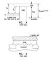
- FIG. 1Afloating gate
- U.S. Pat. No. 5,801,401 by L. Forbesentitled “FLASH MEMORY WITH MICROCRYSTALLINE SILICON CARBIDE AS THE FLOATING GATE STRUCTURE.”
- Another exampleis provided in U.S. Pat. No. 5,852,306 by L. Forbes, entitled “FLASH MEMORY WITH NANOCRYSTALLINE SILICON FILM AS THE FLOATING GATE.”
- Still further examples of this approachare provided in pending applications by L. Forbes and K.
- FIG. 1BAn example of the use of the structured surface approach (FIG. 1B) is provided in U.S. Pat. No. 5,981,350 by J. Geusic, L. Forbes, and K. Y. Ahn, entitled “DRAM CELLS WITH A STRUCTURE SURFACE USING A SELF STRUCTURED MASK.” Another example is provided in U.S. Pat. No. 6,025,627 by L. Forbes and J. Geusic, entitled “ATOMIC LAYER EXPITAXY GATE INSULATORS AND TEXTURED SURFACES FOR LOW VOLTAGE FLASH MEMORIES.”
- FIG. 1Camorphous SiC gate insulators
- graded composition insulatorsto increase the tunneling probability and reduce erase time have been described by the same inventors. (See, L. Forbes and J. M. Eldridge, “GRADED COMPOSITION GATE INSULATORS TO REDUCE TUNNELING BARRIERS IN FLASH MEMORY DEVICES,” application serial no. ______.
- a depletion mode non-volatile memory cellor floating gate transistor, includes a first source/drain region and a second source/drain region separated by a channel region in a substrate.
- a floating gateopposes the channel region and is separated therefrom by a gate oxide.
- a control gateopposes the floating gate. The control gate is separated from the floating gate by an asymmetrical low tunnel barrier intergate insulator.
- the low tunnel barrier intergate insulatorincludes a metal oxide insulator selected from the group consisting of Al 2 O 3 , Ta 2 O 5 , TiO 2 , ZrO 2 , Nb 2 O 5 , SrBi 2 Ta 2 O 3 , SrTiO 3 , PbTiO 3 , and PbZrO 3 .
- the floating gateincludes a polysilicon floating gate having a metal layer formed thereon in contact with the low tunnel barrier intergate insulator.
- the control gateincludes a polysilicon control gate having a metal layer, having a different work function from the metal layer formed on the floating gate, formed thereon in contact with the low tunnel barrier intergate insulator.
- FIGS. 1 A- 1 Cillustrate a number of previous methods for reducing tunneling barriers in Flash memory.
- FIG. 2illustrates one embodiment of a floating gate transistor, or non-volatile memory cell, according to the teachings of the present invention.
- FIG. 3illustrates another embodiment of a floating gate transistor, or non-volatile memory cell, according to the teachings of the present invention.
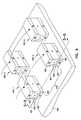
- FIG. 4is a perspective view illustrating an array of silicon pillars formed on a substrate as used in one embodiment according to the teachings of the present invention.
- FIGS. 5 A- 5 Eare cross sectional views taken along cut line 5 - 5 from FIG. 4 illustrating a number of floating gate and control gate configurations which are included in the scope of the present invention.
- FIGS. 6 A- 6 Dillustrate a number of address coincidence schemes can be used together with the present invention.
- FIG. 7Ais an energy band diagram illustrating the band structure at vacuum level with the low tunnel barrier interpoly insulator according to the teachings of the present invention.
- FIG. 7Bis an energy band diagram illustrating the band structure during an erase operation of electrons from the floating gate to the control gate across the low tunnel barrier interpoly insulator according to the teachings of the present invention.
- FIG. 7Cis a graph plotting tunneling currents versus the applied electric fields (reciprocal applied electric field shown) for an number of barrier heights.
- FIG. 8illustrates a block diagram of an embodiment of an electronic system 801 according to the teachings of the present invention.
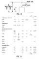
- FIG. 9is a table which provides relevant data on the barrier heights, energy gaps, dielectric constants and electron affinities of a wide variety of metal oxides that could be used as asymmetric tunnel barriers according to the teachings of the present invention.
- FIG. 10is a table which illustrates that there are many stable, crystalline metal oxides whose compositions can vary over at least small compositional ranges.
- FIG. 11is a table which illustrates that work function values can vary considerably, depending on the metal and measurement method.
- FIG. 12illustrates a hypothetical metal-oxide (M—O) phase diagram according to the teachings of the present invention.
- FIGS. 13 A- 13 Cillustrate the compositional profiles for the asymmetrical low tunnel barrier intergate insulators according to the teachings of the present invention.
- FIG. 14illustrates a block diagram of an embodiment of an electronic system according to the teachings of the present invention.
- wafer and substrateare interchangeably used to refer generally to any structure on which integrated circuits are formed, and also to such structures during various stages of integrated circuit fabrication. Both terms include doped and undoped semiconductors, epitaxial layers of a semiconductor on a supporting semiconductor or insulating material, combinations of such layers, as well as other such structures that are known in the art.
- the term “horizontal” as used in this applicationis defined as a plane parallel to the conventional plane or surface of a wafer or substrate, regardless of the orientation of the wafer or substrate.
- the term “vertical”refers to a direction perpendicular to the horizontal as defined above. Prepositions, such as “on”, “side” (as in “sidewall”), “higher”, “lower”, “over” and “under” are defined with respect to the conventional plane or surface being on the top surface of the wafer or substrate, regardless of the orientation of the wafer or substrate.
- the present inventiondescribes the use of asymmetrical metal oxide interpoly dielectric insulators between the control gate and the floating gate of depletion mode non-volatile memory cells.
- An exampleis shown in FIG. 2 for a planar structure, or horizontal depletion mode non-volatile memory cell.
- This non-volatile memory cell, as described herein,can then be implemented in a number of programmable array type logic and/or memory devices according to the teachings of the present invention.
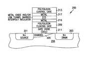
- FIG. 2illustrates one embodiment of a depletion mode floating gate transistor, or depletion mode non-volatile memory cell 200 , according to the teachings of the present invention.
- the deviceworks in the depletion mode and thus is normally on or conducts under zero or negative applied gate voltages.
- the depletion mode non-volatile memory cell 200includes a first source/drain region 201 and a second source/drain region 203 separated by a channel region 205 in a substrate 206 .
- a floating gate 209opposes the channel region 205 and is separated therefrom by a gate oxide 211 .
- a control gate 213opposes the floating gate 209 .
- the control gate 213is separated from the floating gate 209 by an asymmetrical low tunnel barrier intergate insulator 215 .
- the asymmetrical low tunnel barrier intergate insulator 215includes an asymmetrical metal oxide insulator which is aluminum oxide (Al 2 O 3 ).
- the asymmetrical low tunnel barrier intergate insulator 215includes an asymmetrical transition metal oxide selected from the group consisting of Ta 2 O 5 , TiO 2 , ZrO 2 , and Nb 2 O 5 .
- the asymmetrical low tunnel barrier intergate insulator 215includes an asymmetrical Perovskite oxide tunnel barrier selected from the group consisting of SrBi 2 Ta 2 O 3 , SrTiO 3 , PbTiO 3 , and PbZrO 3
- the floating gate 209includes a polysilicon floating gate 209 having a metal layer 216 formed thereon in contact with the asymmetrical low tunnel barrier intergate insulator 215 .
- the control gate 213includes a polysilicon control gate 213 having a metal layer 217 , having a work function different from the metal layer 216 formed on the floating gate 209 , formed thereon in contact with the asymmetrical low tunnel barrier intergate insulator 215 .
- metal layer 216is formed of the same metal material used to form the asymmetrical metal oxide interpoly insulator 215 .
- the depletion mode non-volatile memory cellas described herein, can then be implemented in a number of programmable array type logic and/or memory devices according to the teachings of the present invention.
- FIG. 3illustrates another embodiment of a depletion mode floating gate transistor, or depletion mode non-volatile memory cell 300 , according to the teachings of the present invention.
- the depletion mode non-volatile memory cell 300includes a vertical depletion mode non volatile memory cell 300 .
- the non-volatile memory cell 300has a first source/drain region 301 formed on a substrate 306 .
- a body region 307 including a channel region 305is formed on the first source/drain region 301 .
- a second source/drain region 303is formed on the body region 307 .
- a floating gate 309opposes the channel region 305 and is separated therefrom by a gate oxide 311 .
- a control gate 313opposes the floating gate 309 . According to the teachings of the present invention, the control gate 313 is separated from the floating gate 309 by an asymmetrical low tunnel barrier intergate insulator 315 .
- low tunnel barrier intergate insulator 315includes an asymmetrical metal oxide insulator which is aluminum oxide (Al 2 O 3 ).
- the asymmetrical low tunnel barrier intergate insulator 315includes an asymmetrical transition metal oxide selected from the group consisting of Ta 2 O 5 , TiO 2 , ZrO 2 , and Nb 2 O 5 .
- the low tunnel barrier intergate insulator 315includes an asymmetrical Perovskite oxide tunnel barrier selected from the group consisting of SrBi 2 Ta 2 O 3 , SrTiO 3 , PbTiO 3 , and PbZrO 3 .
- the floating gate 309includes a polysilicon floating gate 309 having a metal layer 316 formed thereon in contact with the asymmetrical low tunnel barrier intergate insulator 315 .
- the control gate 313includes a polysilicon control gate 313 having a metal layer 317 , having a work function different from the metal layer 316 formed on the floating gate 309 , formed thereon in contact with the asymmetrical low tunnel barrier intergate insulator 315 .
- the depletion mode non-volatile memory cellas described herein, can then be implemented in a number of programmable array type logic and/or memory devices according to the teachings of the present invention.
- the floating gate 309includes a vertical floating gate 309 formed alongside of the body region 307 .
- the control gate 313includes a vertical control gate 313 formed alongside of the vertical floating gate 309 .
- the floating gate 309 and control gate 313 orientation shown in FIG. 3is just one embodiment for a vertical non volatile memory cell 300 , according to the teachings of the present invention.
- the floating gateincludes a horizontally oriented floating gate formed alongside of the body region.
- the control gateincludes a horizontally oriented control gate formed above the horizontally oriented floating gate.
- FIG. 4is a perspective view illustrating an array of silicon pillars 400 - 1 , 400 - 2 , 400 - 3 , . . . , 400 -N, formed on a substrate 406 as used in one embodiment according to the teachings of the present invention.
- the substratescan be (i) conventional p-type bulk silicon or p-type epitaxial layers on p+ wafers, (ii) silicon on insulator formed by conventional SIMOX, wafer bonding and etch back or silicon on sapphire, or (iii) small islands of silicon on insulator utilizing techniques such as described in more detail in U.S. Pat. No. 5,691,230, by Leonard Forbes, entitled “Technique for Producing Small Islands of Silicon on Insulator,” issued Nov. 25, 1997, which is incorporated herein by reference.
- each pillar in the array of silicon pillars 400 - 1 , 400 - 2 , 400 - 3 , . . . , 400 -Nincludes a first source/drain region 401 and a second source/drain region 403 .
- the first and the second source/drain regions, 401 and 403are separated by a body region 407 including channel regions 405 .
- a number of trenches 430separate adjacent pillars in the array of silicon pillars 400 - 1 , 400 - 2 , 400 - 3 , . . . , 400 -N.
- Trenches 430are referenced in connection with the discussion which follows in connection with FIGS. 5 A- 5 E.
- FIG. 5Aillustrates one such embodiment of the present invention.
- FIG. 5Aillustrates a first source/drain region 501 and second source/drain region 503 for a non-volatile memory cell 500 formed according to the teachings of the present invention.
- the first and second source/drain regions, 501 and 503are contained in a pillar of semiconductor material, and separated by a body region 507 including channel regions 505 .
- the first source/drain region 501is integrally connected to a buried sourceline 525 .
- the buried sourceline 525is be formed of semiconductor material which has the same doping type as the first source/drain region 501 .
- the sourceline 525is formed of semiconductor material of the same doping as the first source/drain region 501 , but is more heavily doped than the first source/drain region 501 .
- a pair of floating gates 509 - 1 and 509 - 2are formed in each trench 530 between adjacent pillars which form memory cells 500 - 1 and 500 - 2 .
- Each one of the pair of floating gates, 509 - 1 and 509 - 2respectively opposes the body regions 507 - 1 and 507 - 2 in adjacent pillars 500 - 1 and 500 - 2 on opposing sides of the trench 530 .
- a single control gate 513is shared by the pair of floating gates 509 - 1 and 509 - 2 on opposing sides of the trench 530 .
- the shared single control gate 513can include an integrally formed control gate line.
- an integrally formed control gate line 513can be one of a plurality of control gate lines which are each independently formed in the trench, such as trench 530 , below the top surface of the pillars 500 - 1 and 500 - 2 and between the pair of floating gates 509 - 1 and 509 - 2 .
- each floating gatee.g. 509 - 1 and 509 - 2 , includes a vertically oriented floating gate having a vertical length of less than 100 nanometers.
- a pair of floating gates 509 - 1 and 509 - 2are formed in each trench 530 between adjacent pillars which form memory cells 500 - 1 and 500 - 2 .
- Each one of the pair of floating gates, 509 - 1 and 509 - 2respectively opposes the body regions 507 - 1 and 507 - 2 in adjacent pillars 500 - 1 and 500 - 2 on opposing sides of the trench 530 .
- a plurality of control gate linesare again formed in trenches, e.g. trench 530 , below the top surface of the pillars, 500 - 1 and 500 - 2 , and between the pair of floating gates 509 - 1 and 509 - 2 .
- each trenche.g. 530
- Each one of the pair of control gate lines 513 - 1 and 513 - 2addresses the floating gates, 509 - 1 and 509 - 2 respectively, on opposing sides of the trench 530 .
- the pair of control gate lines, or control gates 513 - 1 and 513 - 2are separated by an insulator layer.
- a pair of floating gates 509 - 1 and 509 - 2are again formed in each trench 530 between adjacent pillars which form memory cells 500 - 1 and 500 - 2 .
- Each one of the pair of floating gates, 509 - 1 and 509 - 2respectively opposes the body regions 507 - 1 and 507 - 2 in adjacent pillars 500 - 1 and 500 - 2 on opposing sides of the trench 530 .
- the plurality of control gate linesare disposed vertically above the floating gates. That is, in one embodiment, the control gate lines are located above the pair of floating gates 509 - 1 and 509 - 2 and not fully beneath the top surface of the pillars 500 - 1 and 500 - 2 . In the embodiment of FIG. 5C, each pair of floating gates, e.g. 509 - 1 and 509 - 2 , in a given trench shares a single control gate line, or control gate 513 .
- a pair of floating gates 509 - 1 and 509 - 2are formed in each trench 530 between adjacent pillars which form memory cells 500 - 1 and 500 - 2 .
- Each one of the pair of floating gates, 509 - 1 and 509 - 2respectively opposes the body regions 507 - 1 and 507 - 2 in adjacent pillars 500 - 1 and 500 - 2 on opposing sides of the trench 530 .
- the plurality of control gate linesare disposed vertically above the floating gates. That is, in one embodiment, the control gate lines are located above the pair of floating gates 509 - 1 and 509 - 2 and not fully beneath the top surface of the pillars 500 - 1 and 500 - 2 . However, in the embodiment of FIG. 5D, each one of the pair of floating gates, e.g. 509 - 1 and 509 - 2 , is addressed by an independent one of the plurality of control lines or control gates, shown in FIG. 5D as 513 - 1 and 513 - 2 .
- a single floating gate 509is formed in each trench 530 between adjacent pillars which form memory cells 500 - 1 and 500 - 2 .
- the single floating gate 509can be either a vertically oriented floating gate 509 or a horizontally oriented floating gate 509 formed by conventional processing techniques, or can be a horizontally oriented floating gate 509 formed by a replacement gate technique such as described in a copending application, entitled “Flash Memory with Ultrathin Vertical Body Transistors,” by Leonard Forbes and Kie Y. Ahn, application Ser. No. 09/780,169.
- the floating gate 509has a vertical length facing the body region 505 of less than 100 nm. In another embodiment, the floating gate 509 has a vertical length facing the body region 505 of less than 50 nm. In one embodiment, as shown in FIG. 5E, the floating gate 509 is shared, respectively, with the body regions 507 - 1 and 507 - 2 , including channel regions 505 - 1 and 505 - 2 , in adjacent pillars 500 - 1 and 500 - 2 located on opposing sides of the trench 530 . In one embodiment, the control gate 513 includes a horizontally oriented control gate 513 formed above the horizontally oriented floating gate 509 .
- the floating gates 509are separated from the control gate lines, or control gates 513 with an asymmetrical low tunnel barrier intergate insulator in accordance with the descriptions given above in connection with FIG. 3.
- the modifications hereare to use tunneling through the interpoly dielectric to realize flash memory devices.
- the vertical devicesinclude an extra flexibility in that the capacitors, e.g. gate oxide and intergate insulator, are easily fabricated with different areas. This readily allows the use of very high dielectric constant inter-poly dielectric insulators with lower tunneling barriers.
- FIGS. 6 A- 6 Dillustrate that a number of address coincidence schemes can be used together with the present invention.
- FIG. 6Aillustrates a NOR flash memory array 610 having a number of non-volatile memory cells 600 - 1 , 600 - 2 , 600 - 3 , using a coincidence address array scheme.
- FIG. 6Ashows a sourceline 625 coupled to a first source/drain region 601 in each of the number of non-volatile memory cells 600 - 1 , 600 - 2 , 600 - 3 .
- the sourcelineis shown oriented in a first selected direction in the flash memory array 610 .
- FIG. 6Aa number of control gate lines 630 are shown oriented in a second selected direction in the flash memory array 610 .
- the number of control gate lines 630are coupled to, or integrally formed with the control gates 613 for the number of non-volatile memory cells 600 - 1 , 600 - 2 , 600 - 3 .
- the second selected directionis orthogonal to the first selected direction.
- FIG. 6Ashows a number of bitlines 635 oriented in a third selected direction in the flash memory array 610 . As shown in FIG.
- the number of bitlinesare coupled to the second source/drain regions in the number of non-volatile memory cells 600 - 1 , 600 - 2 , 600 - 3 .
- the third selected directionis parallel to the second selected direction and the number of control gate lines 630 serve as address lines.
- the flash memory array 610includes a number of backgate or substrate/well bias address lines 640 coupled to the substrate.
- FIGS. 6 B- 6 Dillustrate of top view for three different coincidence address scheme layouts suitable for use with the present invention.
- FIG. 6Bprovides the top view layout of the coincidence address scheme described in connection with FIG. 6A. That is, FIG. 6B illustrates a number of sourcelines 625 oriented in a first selected direction, a number of control gate lines 630 oriented in a second selected direction, and a number of bitlines 635 oriented in a third selected direction for the flash memory array 600 .
- the second and third selected directionare parallel to one another and orthogonal to the first selected direction such that the number of control gate lines 630 serve as address lines.
- FIG. 6Cprovides the top view layout of another coincidence address scheme according to the teachings of the present invention.
- FIG. 6Cillustrates a number of sourcelines 625 oriented in a first selected direction, a number of control gate lines 630 oriented in a second selected direction, and a number of bitlines 635 oriented in a third selected direction for the flash memory array 600 .
- the first selected direction and the third selected directionare parallel to one another and orthogonal to the second selected direction.
- the number of control gate lines 630again serve as address lines.
- FIG. 6Dprovides the top view layout of yet another coincidence address scheme according to the teachings of the present invention.
- FIG. 6Dillustrates a number of sourcelines 625 oriented in a first selected direction, a number of control gate lines 630 oriented in a second selected direction, and a number of bitlines 635 oriented in a third selected direction for the flash memory array 600 .
- the first selected direction and the second selected directionare parallel to one another and orthogonal to the third selected direction.
- the number of bitlines 635serve as address lines.
- writecan still be achieved by hot electron injection and/or, according to the teachings of the present invention, tunneling from the control gate to the floating gate.
- block eraseis accomplished by driving the control gates with a relatively large positive voltage and tunneling from the metal on top of the floating gate to the metal on the bottom of the control gate.
- FIG. 7Ais an energy band diagram illustrating the band structure at vacuum level with the asymmetrical low tunnel barrier interpoly insulator according to the teachings of the present invention.
- FIG. 7Ais useful in illustrating the reduced tunnel barrier off of the floating gate to the control gate and for illustrating the respective capacitances of the structure according to the teachings of the present invention.
- FIG. 7Ashows the band structure of the silicon substrate, e.g. channel region 701 , silicon dioxide gate insulator, e.g. gate oxide 703 , polysilicon floating gate 705 , the asymmetrical low tunnel barrier interpoly dielectric 707 , between metal plates 709 and 711 , and then the polysilicon control gate 713 , according to the teachings of the present invention.
- the design considerations involvedare determined by the dielectric constant, thickness and tunneling barrier height of the asymmetrical interpoly dielectric insulator 707 relative to that of the silicon dioxide gate insulator, e.g. gate oxide 703 .
- the tunneling probability through the interpoly dielectric 707is an exponential function of both the barrier height and the electric field across this dielectric.
- FIG. 7Bis an energy band diagram illustrating the band structure during an erase operation of electrons from the floating gate 705 to the control gate 713 across the low tunnel barrier interpoly insulator 707 according to the teachings of the present invention.
- FIG. 7Bis similarly useful in illustrating the reduced tunnel barrier off of the floating gate 705 to the control gate 713 and for illustrating the respective capacitances of the structure according to the teachings of the present invention.
- the electric fieldis determined by the total voltage difference across the structure, the ratio of the capacitances (see FIG. 7A), and the thickness of the asymmetrical interpoly dielectric 707 .
- Eis the electric field across the interpoly dielectric insulator 707 and Eo depends on the barrier height.
- the lower electric field in the aluminum oxide interpoly insulator 707 for the same current densityreflects the lower tunneling barrier of approximately 2 eV, shown in FIG. 7B, as opposed to the 3.2 eV tunneling barrier of silicon oxide 703 , also illustrated in FIG. 7B.
- FIG. 7Cis a graph plotting tunneling currents versus the applied electric fields (reciprocal applied electric field shown) for a number of barrier heights.
- FIG. 7Cillustrates the dependence of the tunneling currents on electric field (reciprocal applied electric field) and barrier height.
- the fraction of voltage across the asymmetrical interpoly or asymmetrical intergate insulator, ⁇ V 2can be increased by making the area of the intergate capacitor, C 2 , (e.g. intergate insulator 707 ) smaller than the area of the transistor gate capacitor, C 1 (e.g. gate oxide 703 ). This would be required with high dielectric constant intergate dielectric insulators 707 and is easily realized with the vertical floating gate structures described above in connection with FIGS. 3 , and 5 A- 5 E.
- the poly-Si layeris to be formed with emphasis on obtaining a surface that is very smooth and morphologically stable at subsequent device processing temperatures which will exceed that used to grow Metal oxide.
- the oxide growth rate and limiting thicknesswill increase with oxidation temperature and oxygen pressure.
- the oxidation kinetics of a metalmay, in some cases, depend on the crystallographic orientations of the very small grains of metal which comprise the metal film (see generally, O, Kubaschewski and B. E. Hopkins, “Oxidation of Metals and Alloys”, Butterworth, London, pp. 53-64, 1962). If such effects are significant, the metal deposition process can be modified in order to increase its preferred orientation and subsequent oxide thickness and tunneling uniformity. To this end, use can be made of the fact that metal films strongly prefer to grow during their depositions having their lowest free energy planes parallel to the film surface. This preference varies with the crystal structure of the metal. For example, fcc metals prefer to form ⁇ 111 ⁇ surface plans. Metal orientation effects, if present, would be larger when only a limited fraction of the metal will be oxidized and unimportant when all or most of the metal is oxidized.
- Tunnel barrierscomprised of metal oxide films and having different heights at their two interfaces with the contact electrodes can be made by properly oxidizing the parent metal films. Not all oxides will exhibit asymmetrical barrier characteristics. Asymmetrical barriers can be formed on those oxides that are stable over small composition ranges so that gradients can be formed which produce different barrier heights at the top and bottom contacts.
- SiO 2 and PbO films, made by conventional processes,are stable only at their stoichiometric compositions: hence, they can only serve as symmetrical barriers.
- there are many stable, crystalline metal oxideswhose compositions can vary over at least small compositional ranges. The same is evidenced in the table shown in FIG.
- a second approach for forming an asymmetric barrieris to employ a control contact plate that has a different work function than that under the metal oxide dielectric layer.
- very asymmetric barrierscan be produced by judicious selection of contact metals since their work functions can vary from low values of ⁇ 2.7 eV for rare earth metals to ⁇ 5.8 eV for platinum.
- S. M. Sze“Physics of Semiconductor Devices,” 2nd Edition, Wiley-Interscience, N.Y., pp. 553-556, 1981. Note that the reported work function values can vary considerably, depending on the metal and measurement method. The same is evidenced in the table shown in FIG.
- FIG. 8graphically illustrates the dependence of the barrier height for current injection on the work function and electron affinity of a given, homogeneous dielectric film.
- FIG. 9is a table which provides relevant data on the barrier heights, energy gaps, dielectric constants and electron affinities of a wide variety of metal oxides that could be used as asymmetric tunnel barriers according to the teachings of the present invention. (See generally, H.F. Luan et al., “High quality Ta 2 O 5 gate dielectrics with T ox equil. 10 Angstroms,” IEDM Tech. Digest, pp. 141-144, 1999; J.
- Robertson et al.“Schottky barrier heights of tantalum oxide, barium strontium titanate, lead titanate and strontium bismuth tantalate,” App. Phys. Lett., Vol. 74, No. 8, pp. 1168-1170, Feb. 1999; J. Robertson, “Band offsets of wide-band-gap oxides and implications for future electronic devices,” J. Vac. Sci. Technol. B, Vol. 18, No. 3, pp. 1785-1791, 2000; Xin Guo et al., “High quality ultra-thin (1.5 nm) TiO 2 /Si 3 N 4 gate dielectric for deep submicron CMOS technology,” IEDM Tech. Digest, pp.
- TM oxidesTransition Metal oxides
- Table 1Other properties of some simple Transition Metal oxides (TM oxides) have been shown in the table provided in FIG. 10. Note that their compositions can vary from metal-rich to their stoichiometric values. This, along with related, established oxidation data and theory (see generally, the comprehensive review by O. Kubaschewski and B.E. Hopkins, “Oxidation of Metals and Alloys,” Butterworth, London (1962)) and the thermodynamic properties of solid multi-component solid systems (see, for example, R. A. Swalin, “Thermodynamics of Solids, 2nd Ed.” chap. 8, pp. 165-180, John Wiley and Sons, 1972) lead to the rigorous understanding required to uniquely and controllably form asymmetrical oxide tunnel barriers as used by the present invention. Further explanation is as follows:
- compositional ranges shown in the table of FIG. 10are for thermodynamically-stable, bulk, crystalline TM oxides and should be taken as approximate values only. Ultra-thin TM oxide films may be stable over wider compositional ranges owing to surface energy and other effects.
- TM(O)The solid solubility of O in each TM is large, relative to most metal-oxygen systems.
- This phaseis designated as TM(O) and forms when the TM film is exposed to oxygen. As such, this phase lies under and is in immediate contact with the growing oxide layer. Note, however, that high levels of oxygen solubility in the metals is not a pre-requisite for the present invention.
- FIG. 12illustrates a hypothetical metal-oxide (M-O) phase diagram according to the teachings of the present invention.
- composition of the TM(O) in contact with TM oxideis C 1 0 .
- the thickness of this saturated layerneed only be a few monolayers or less but it must be present in order for oxide to grow on the underlying metal.
- composition of the TM oxide in contact with TM(O)is C 2 0 .
- composition of the TM oxide in contact with O 2is C 3 0 .
- Xis oxide thickness.
- thermodynamic effects in these metal-oxide systemsserve to produce the desired concentration gradients across the oxide films.
- an asymmetric tunnel barriercan be grown by low temperature thermal oxidation of a large number of metal films provided some finite thickness of metal is left unoxidized in order to fix the inner composition of the growing oxide film.
- the oxide composition and composition gradient thereinwill depend on the thermodynamic properties of metal-oxide system involved.
- FIGS. 13 A- 13 Cillustrate the compositional profiles for the asymmetrical low tunnel barrier intergate insulators according to the teachings of the present invention.
- FIG. 13Ashows the compositional profile before oxidation.
- FIG. 13Bshows the compositional profile during oxidation with the coexisting phases indicated.
- FIG. 13Cshows the compositional profile at the end of oxidation.
- the conventional large barrier insulating dielectricsare silicon oxide and silicon nitride.
- silicon oxideis not an optimum choice for memory type devices, because the 3.2eV tunnel barrier is too high resulting in premature failure of the insulators and limiting the number of operational cycles to be in the order of 10 5 to 10 7 .
- an asymmetrical low tunneling barrier interpoly insulatoris used instead, such as Al 2 O 3 with a tunneling barrier of approximately 2.0 eV.
- a number of studieshave dealt with electron tunneling in Al/Al 2 O 3 /Al structures where the oxide was grown by “low temperature oxidation” in either molecular or plasma oxygen. (See generally, S. M. Sze, Physics of Semiconductor Devices, Wiley, N.Y., pp. 553-556, 1981; G. Simmons and A. El-Badry, “Generalized formula for the electric tunnel effect between similar electrodes separated by a thin insulating film,” J. Appl. Phys., Vol. 34, p. 1793, 1963; S.
- Tunnel currentsare asymmetrical in this system with somewhat larger currents flowing when electrons are injected from Al/Al 2 O 3 interface developed during oxide growth. This asymmetry is due to a minor change in composition of the growing oxide: there is a small concentration of excess metal in the Al 2 O 3 , the concentration of which diminishes as the oxide is grown thicker. The excess Al +3 ions produce a space charge that lowers the tunnel barrier at the inner interface. The oxide composition at the outer Al 2 O 3 /Al contact is much more stoichiometric and thus has a higher tunnel barrier. In situ ellipsometer measurements on the thermal oxidation of Al films deposited and oxidized in situ support this model (see generally, J. Grimblot and J.
- (ii)Oxidize the aluminum in situ in molecular oxygen using temperatures, pressure and time to obtain the desired Al 2 O 3 thickness.
- the thicknessincreases with log (time) and can be controlled via time at a fixed oxygen pressure and temperature to within 0.10 Angstroms, when averaged over a large number of aluminum grains that are present under the counter-electrode.
- the oxidewill be amorphous and remain so until temperatures in excess of 400 degrees Celsius are reached.
- the initiation of recrystallization and grain growthcan be suppressed, if desired, via the addition of small amounts of glass forming elements (e.g., Si) without altering the growth kinetics or barrier heights significantly.
- this oxide insulatoris used as an asymmetrical low tunnel barriers, of the order of 2.0 eV, as the inter-poly or inter-gate dielectric insulators.
- the characteristics of such oxide insulatorshave been summarized in FIG. 9.
- asymmetrical low barriersare utilized in programmable array logic or memory device which are easy to write and/or erase.
- different contact metalsas for instance aluminum (Al) and platinum (Pt) may be used as illustrated in FIGS. 2 and 3.
- the floating gateincludes a polysilicon floating gate having a metal layer formed thereon in contact with the asymmetrical low tunnel barrier intergate insulator.
- the control gateincludes a polysilicon control gate with a metal layer, having a work function different from that of the metal layer formed on the floating gate, formed thereon in contact with the asymmetrical low tunnel barrier intergate insulator.
- the asymmetrical low tunnel barrier interpoly insulatoris formed such that the tunnel barrier is approximately 2.0 eV.
- single layers of Ta 2 O 5 , TiO 2 , ZrO 2 , Nb 2 O 5 and similar transition metal oxidescan be formed by “low temperature oxidation” of numerous Transition Metal (e.g., TM oxides) films in molecular and plasma oxygen and also by rf sputtering in an oxygen plasma.
- TM oxidesTransition Metal
- the thermal oxidation kinetics of these metalshave been studied for decades with numerous descriptions and references to be found in the book by Kubaschewski and Hopkins (see generally, O. Kubaschewski and B. E. Hopkins, “Oxidation of Metals and Alloys”, Butterworth, London, pp. 53-64, 1962).
- Such metalsoxidize via logarithmic kinetics to reach thicknesses of a few to several tens of angstroms in the range of 100 to 300 degrees Celsius.
- Excellent oxide barriers for Josephson tunnel devicescan be formed by rf sputter etching these metals in an oxygen plasma (see generally, J. M. Greiner, “Josephson tunneling barriers by rf sputter etching in an oxygen plasma,” J. Appl. Phys., Vol. 42, No. 12, pp. 5151-5155, 1971; O. Michikami et al., “Method of fabrication of Josephson tunnel junctions,” U.S. Pat. No. 4,412,902, Nov. 1, 1983).
- this treatmentcan be carried out in an inert gas atmosphere, thus lessening the possibility of inadvertently oxidizing the poly-Si floating gate.
- this earlier disclosurewas directed at developing methods and procedures for producing high dielectric constant films for storage cells for DRAMs, the same teachings can be applied to producing thinner asymmetrical metal oxide tunnel films for the programmable array logic and memory devices described in this disclosure.
- the dielectric constants of these TM oxidesare substantially greater (>25 to 30 or more) than those of PbO and Al 2 O 3 .
- Duplex layers of these high dielectric constant oxide filmsare easily fabricated with simple tools and also provide improvement in device yields and reliability. Each oxide layer will contain some level of defects but the probability that such defects will overlap is exceedingly small.
- TM and their oxidesare highly refractory and etchable (e.g., by RIE). Hence they are quite compatible with poly-Si control gate processes and other subsequent steps.
- TM silicide formationwill not occur during the oxidation step. It could take place at a significant rate at the temperatures used to deposit the poly-Si control gate. If so, several solutions can be applied including:
- Insulator and contact metal layer combinationse.g. platinum (Pt) and aluminum (Al), or other contact metals with different work functions with appropriate barrier heights, according to the teachings of the present invention, have been shown in FIG. 9.
- the asymmetrical transition metal oxide interpoly insulatorscan be formed having a tunnel barrier of approximately 2.0 eV as required by the present invention.
- Asymmetrical oxide tunnel barriers having a wide range of propertiescan also be grown via oxidation of alloy films of appropriate compositions (see generally, J. Robertson and C. W. Chen, “Schottky barrier heights of tantalum oxide, barium strontium titanate, lead titanate, and strontium bismuth tantalate,” Appl. Phys. Lett., vol. 74, no. 8, pp. 1168-1170, Feb. 22, 1999) and as referenced in the co-pending, co-filed application by L. Forbes and J. M. Eldridge, entitled “FLASH MEMORY DEVICES WITH METAL OXIDE INTERPLOY INSULATORS,” attorney docket number 1303.014us1. Thin film barriers of platinum, palladium and similar noble metals must be added to prevent inter-diffusion and degradation of the perovskite oxides with the poly-Si layers.
- the dielectric constants of crystallized, perovskite oxidescan be very large, with values in the 100 to 1000 or more range.
- the basic processis more complicated than that needed to oxidize layered films of transition metals.
- the TM layerswould typically be pure metals although they could be alloyed.
- the TMsare similar metallurgically as are their oxides.
- the parent alloy films that can be converted to a perovskite oxideare typically comprised of metals having widely different chemical reactivities with oxygen and other common gasses.
- Y—Ba—Cu system referenced aboveY and Ba are among the most reactive of metals while the reactivity of Cu approaches (albeit distantly) those of other noble metals.
- the alloyis to be completely oxidized, then thin film barriers such as Pd, Pt, etc. or their conductive oxides must be added between the Si and the parent metal film to serve as: electrical contact layers; diffusion barriers; and, oxidation stops.
- the Schottky barrier heights of various TM oxides and perovskite oxides in contact with various metalswill help in the design of the tunnel device.
- the barrier heightswill represent that developed during oxide growth at the parent perovskite alloy/perovskite oxide interface. Obviously, such barrier heights cannot be predicted ab initio for such a wide class of materials but will have to be developed as the need arises. This information will have to be developed on a system-by-system basis.
- top metalwill be determined by the desired offset voltages that are to be applied to write and erase the device. Great caution must be applied to prevent unwanted impurity segregation during the deposition of the top electrode material or during subsequent device processing treatments. In many cases, this can be accomplished by depositing the top electrode metal from an Ultra-Pure source. This may not be sufficient for producing top electrode metals having sufficiently controlled work functions. In such cases, the problem can be solved by depositing the metal under a low partial pressure of oxygen. The oxygen is to be introduced after the first several monolayers of metals have been deposited.
- the top electrode metalcan be formed with a very modest level of internal oxidation that will substantially block impurities from diffusing to the inner interface and thus alter the desired work function.
- Levels of oxygen up to a few percentgenerally have no perceptible effect on metal conductivity at ambient temperatures and above.
- Writecan be achieved by tunneling from the control gate to the floating gate by driving the control gate negative and/or channel hot electron injection as in conventional flash memory devices. Erase would be accomplished by driving the control gates with a relatively large positive voltage and tunneling from the metal on top of the floating gate to the metal on the bottom of the control gate through the asymmetrical low tunnel barrier intergate insulators of the present invention. An asymmetrical low tunnel barrier between the floating gate and the control gate will make the erase operation easy.
- n-channel enhancement mode devicesare used in the array, reading is accomplished by driving the control gate with a smaller positive voltage. If no electrons are stored on the floating gate the transistor will turn on. If electrons are stored on the floating gate the transistor will not turn on or only turn on at a lower conductivity state. This constitutes the memory function. If n-channel depletion mode devices are used in the array then reading of the stored data is accomplished with a zero or negative gate voltage, if the device conducts with zero or negative small gate voltage then there is no charge stored on the floating gate. If the floating gate is charged by stored electrons then the transistor will not conduct with zero or low negative gate voltages.
- the presence of stored charge on the floating gate and/or applied negative gate voltageswill result in electric fields in the interpoly/intergate insulator. If the gate oxide is 2 nm (20 ⁇ ) thick then the capacitance is about 1.6 ⁇ 10 ⁇ 6 F/cm 2 and a 1 Volt difference will store a charge of 1.6 ⁇ 10 ⁇ 6 Coulombs/cm 2 . A retention time of one second requires a leakage current of less than about 10 ⁇ 6 Amps/cm 2 , if as shown in FIG.
- the tunneling barrieris 2.0 eV and the electric field in the interpoly/intergate insulator is less than about 2 ⁇ 10 6 V/cm then the current density will be 10 ⁇ 16 Amps/cm 2 and the retention time 10 +10 seconds.
- One yearis about 3 ⁇ 10 +7 seconds, very long retention times can be achieved by using low electric fields during read in conjunction with the larger tunnel barrier during read.
- the lower tunneling barrierresults in a much faster erase at much lower electric fields and than in conventional flash memory devices which require fields of 10 7 V/cm to achieve the erase currents of 1 Amp/cm 2 with a silicon oxide tunnel barrier of 3.2 eV.
- the asymmetrical tunnel barriers of the present inventioncan serve to make erase of flash memory type devices easy while insuring a long retention time during standby and read operations.
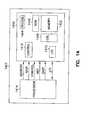
- FIG. 14illustrates a block diagram of an embodiment of an electronic system 1401 according to the teachings of the present invention.
- the system 1401includes a memory device 1400 which has an array of memory cells 1402 , address decoder 1404 , row access circuitry 1406 , column access circuitry 1408 , control circuitry 1410 , and input/output circuit 1412 .
- the circuit 1401includes a processor 1414 , or memory controller for memory accessing.
- the memory device 1400receives control signals from the processor 1414 , such as WE*, RAS* and CAS* signals over wiring or metallization lines.
- the memory device 1400is used to store data which is accessed via I/O lines.
- At least one of the processor 1414 or memory device 1400has a memory cell formed according to the embodiments of the present invention. That is, at least one of the processor 1414 or memory device 1400 includes an asymmetrical low tunnel barrier interpoly insulator according to the teachings of the present invention.
- FIG. 14illustrates an embodiment for electronic system circuitry in which the novel memory cells of the present invention are used.
- the illustration of system 1401is intended to provide a general understanding of one application for the structure and circuitry of the present invention, and is not intended to serve as a complete description of all the elements and features of an electronic system using the novel memory cell structures.
- the inventionis equally applicable to any size and type of memory device 1400 using the novel memory cells of the present invention and is not intended to be limited to that described above.
- such an electronic systemcan be fabricated in single-package processing units, or even on a single semiconductor chip, in order to reduce the communication time between the processor and the memory device.
- Applications containing the novel memory cell of the present invention as described in this disclosureinclude electronic systems for use in memory modules, device drivers, power modules, communication modems, processor modules, and application-specific modules, and may include multilayer, multichip modules.
- Such circuitrycan further be a subcomponent of a variety of electronic systems, such as a clock, a television, a cell phone, a personal computer, an automobile, an industrial control system, an aircraft, and others.
- Asymmetrical low barrier tunnel insulatorsare described between the floating gate and control gate in a flash memory type devices to form programmable array logic and memory devices.
- the asymmetrical low barrier insulators⁇ 2.0 eV, are easily fabricated by the oxidation of a transition metal or a composite metal layer. While the amount of charge stored on the floating gate is small the transistor provides gain and charge multiplication resulting in a large output signal and ease of reading the stored data. If there is an adverse capacitance ratio due to a large difference of dielectric constants then the vertical gate structures described previously can be employed.
- Writecan be achieved by the normal channel hot electron injection and gate current through the silicon oxide to the floating gate. This is done by selecting a particular column by applying a high control gate voltage and applying relatively large drain voltage as is done with conventional ETOX memory devices. However, according to the teachings of the present invention, write can also be accomplished by applying a positive voltage to the substrate or well select line and a large negative voltage to the control gates, electrons will tunnel from the control gate to the floating gate. The asymmetrical low tunnel barrier will provide an easy write operation and the selection of the substrate or well bias will provide selectivity and address only one device.
- eraseis achieved by providing a negative voltage to the substrate or well address line and a large positive voltage to the control gate. This causes electrons to tunnel off of the floating gate on to the control gate.
- a whole rowcan be erased by addressing all the column lines along that row and a block can be erased by addressing multiple row back gate or substrate/well address lines.
- the asymmetrical low tunnel barrier interpoly insulators of the present inventionavoid the large barriers to electron tunneling or hot electron injection presented by the silicon oxide-silicon interface, 3.2 eV, which result in slow write and erase speeds even at very high electric fields.
- the present inventionalso avoids the combination of very high electric fields and damage by hot electron collisions in the which oxide result in a number of operational problems like soft erase error, reliability problems of premature oxide breakdown and a limited number of cycles of write and erase.
- the asymmetrical low tunnel barrier interploy dielectric insulator erase approach, of the present inventionremedies the above mentioned problems of having a rough top surface on the polysilicon floating gate which results in, poor quality interpoly oxides, sharp points, localized high electric fields, premature breakdown and reliability problems.
Landscapes
- Non-Volatile Memory (AREA)
- Semiconductor Memories (AREA)
Abstract
Description
- This application is related to the following co-pending, commonly assigned U.S. patent applications: “DRAM Cells with Repressed Memory Metal Oxide Tunnel Insulators,” attorney docket no. 1303.019US1, serial number ______, “Flash Memory with Low Tunnel Barrier Interpoly Insulators,” attorney docket no. 1303.014US1, serial number ______, “Dynamic Electrically Alterable Programmable Memory with Insulating Metal Oxide Interpoly Insulators,” attorney docket no. 1303.024US1, serial number ______, and “Field Programmable Logic Arrays with Metal Oxide and/or Low Tunnel Barrier Interpoly Insulators,” attorney docket no. 1303.027US1, serial number ______, “SRAM Cells with Repressed Floating Gate Memory, Metal Oxide Tunnel Interpoly Insulators,” attorney docket no. 1303.028US1, serial number ______, “Programmable Memory Address and Decode Devices with Low Tunnel Barrier Interpoly Insulators,” attorney docket no. (Micron 01-0485), serial number ______, which are filed on even date herewith and each of which disclosure is herein incorporated by reference.[0001]
- The present invention relates generally to integrated circuits, and in particular to programmable array type logic and/or memory devices with asymmetrical low tunnel barrier interpoly insulators.[0002]
- Flash memories have become widely accepted in a variety of applications ranging from personal computers, to digital cameras and wireless phones. Both INTEL and AMD have separately each produced about one billion integrated circuit chips in this technology.[0003]
- The original EEPROM or EARPROM and flash memory devices described by Toshiba in 1984 used the interpoly dielectric insulator for erase. (See generally, F. Masuoka et al., “A new flash EEPROM cell using triple polysilicon technology,” IEEE Int. Electron Devices Meeting, San Francisco, pp. 464-67, 1984; F. Masuoka et al., “256K flash EEPROM using triple polysilicon technology,” IEEE Solid-State Circuits Conf., Philadelphia, pp. 168-169, 1985). Various combinations of silicon oxide and silicon nitride were tried. (See generally, S. Mori et al., “reliable CVD inter-poly dialectics for advanced E&EEPROM,” Symp. On VLSI Technology, Kobe, Japan, pp. 16-17, 1985). However, the rough top surface of the polysilicon floating gate resulted in, poor quality interpoly oxides, sharp points, localized high electric fields, premature breakdown and reliability problems.[0004]
- Widespread use of flash memories did not occur until the introduction of the ETOX cell by INTEL in 1988. (See generally, U.S. Pat. No. 4,780,424, “Process for fabricating electrically alterable floating gate memory devices,” Oct. 25, 1988; B. Dipert and L. Hebert, “Flash memory goes mainstream,” IEEE Spectrum, pp. 48-51, October, 1993; R. D. Pashley and S. K. Lai, “Flash memories, the best of two worlds,” IEEE Spectrum, pp. 30-33, December 1989). This extremely simple cell and device structure resulted in high densities, high yield in production and low cost. This enabled the widespread use and application of flash memories anywhere a non-volatile memory function is required. However, in order to enable a reasonable write speed the ETOX cell uses channel hot electron injection, the erase operation which can be slower is achieved by Fowler-Nordhiem tunneling from the floating gate to the source. The large barriers to electron tunneling or hot electron injection presented by the silicon oxide-silicon interface, 3.2 eV, result in slow write and erase speeds even at very high electric fields. The combination of very high electric fields and damage by hot electron collisions in the oxide result in a number of operational problems like soft erase error, reliability problems of premature oxide breakdown and a limited number of cycles of write and erase.[0005]
- Other approaches to resolve the above described problems include; the use of different floating gate materials, e.g. SiC, SiOC, GaN, and GaAIN, which exhibit a lower work function (see FIG. 1A), the use of structured surfaces which increase the localized electric fields (see FIG. 1B), and amorphous SiC gate insulators with larger electron affinity, χ, to increase the tunneling probability and reduce erase time (see FIG. 1C).[0006]
- One example of the use of different floating gate (FIG. 1A) materials is provided in U.S. Pat. No. 5,801,401 by L. Forbes, entitled “FLASH MEMORY WITH MICROCRYSTALLINE SILICON CARBIDE AS THE FLOATING GATE STRUCTURE.” Another example is provided in U.S. Pat. No. 5,852,306 by L. Forbes, entitled “FLASH MEMORY WITH NANOCRYSTALLINE SILICON FILM AS THE FLOATING GATE.” Still further examples of this approach are provided in pending applications by L. Forbes and K. Ahn, entitled “DYNAMIC RANDOM ACCESS MEMORY OPERATION OF A FLASH MEMORY DEVICE WITH CHARGE STORAGE ON A LOW ELECTRON AFFINITY GaN OR GaAIN FLOATING GATE,” Ser. No. 08/908098, and “VARIABLE ELECTRON AFFINITY DIAMOND-LIKE COMPOUNDS FOR GATES IN SILICON CMOS MEMORIES AND IMAGING DEVICES,” Ser. No. 08/903452.[0007]
- An example of the use of the structured surface approach (FIG. 1B) is provided in U.S. Pat. No. 5,981,350 by J. Geusic, L. Forbes, and K. Y. Ahn, entitled “DRAM CELLS WITH A STRUCTURE SURFACE USING A SELF STRUCTURED MASK.” Another example is provided in U.S. Pat. No. 6,025,627 by L. Forbes and J. Geusic, entitled “ATOMIC LAYER EXPITAXY GATE INSULATORS AND TEXTURED SURFACES FOR LOW VOLTAGE FLASH MEMORIES.”[0008]
- Finally, an example of the use of amorphous SiC gate insulators (FIG. 1C) is provided in U.S. patent application Ser. No. 08/903453 by L. Forbes and K. Ahn, entitled “GATE INSULATOR FOR SILICON INTEGRATED CIRCUIT TECHNOLOGY BY THE CARBURIZATION OF SILICON.”[0009]
- Additionally, graded composition insulators to increase the tunneling probability and reduce erase time have been described by the same inventors. (See, L. Forbes and J. M. Eldridge, “GRADED COMPOSITION GATE INSULATORS TO REDUCE TUNNELING BARRIERS IN FLASH MEMORY DEVICES,” application serial no. ______.[0010]
- However, all of these approaches relate to increasing tunneling between the floating gate and the substrate such as is employed in a conventional ETOX device and do not involve tunneling between the control gate and floating gate through and inter-poly dielectric.[0011]
- Therefore, there is a need in the art to provide improved programmable array type logic and/or memory devices while avoiding the large barriers to electron tunneling or hot electron injection presented by the silicon oxide-silicon interface, 3.2 eV, which result in slow write and erase speeds even at very high electric fields. There is also a need to avoid the combination of very high electric fields and damage by hot electron collisions in the which oxide result in a number of operational problems like soft erase error, reliability problems of premature oxide breakdown and a limited number of cycles of write and erase. Further, when using an interpoly dielectric insulator erase approach, the above mentioned problems of having a rough top surface on the polysilicon floating gate which results in, poor quality interpoly oxides, sharp points, localized high electric fields, premature breakdown and reliability problems must be avoided.[0012]
- The above mentioned problems with programmable array type logic and/or memory devices and other problems are addressed by the present invention and will be understood by reading and studying the following specification. Systems and methods are provided for programmable array type logic and/or memory devices with asymmetrical, low tunnel barrier interpoly insulators.[0013]
- In one embodiment of the present invention, a depletion mode non-volatile memory cell, or floating gate transistor, includes a first source/drain region and a second source/drain region separated by a channel region in a substrate. A floating gate opposes the channel region and is separated therefrom by a gate oxide. A control gate opposes the floating gate. The control gate is separated from the floating gate by an asymmetrical low tunnel barrier intergate insulator. The low tunnel barrier intergate insulator includes a metal oxide insulator selected from the group consisting of Al[0014]2O3, Ta2O5, TiO2, ZrO2, Nb2O5, SrBi2Ta2O3, SrTiO3, PbTiO3, and PbZrO3. The floating gate includes a polysilicon floating gate having a metal layer formed thereon in contact with the low tunnel barrier intergate insulator. And, the control gate includes a polysilicon control gate having a metal layer, having a different work function from the metal layer formed on the floating gate, formed thereon in contact with the low tunnel barrier intergate insulator.
- These and other embodiments, aspects, advantages, and features of the present invention will be set forth in part in the description which follows, and in part will become apparent to those skilled in the art by reference to the following description of the invention and referenced drawings or by practice of the invention. The aspects, advantages, and features of the invention are realized and attained by means of the instrumentalities, procedures, and combinations particularly pointed out in the appended claims.[0015]
- FIGS.[0016]1A-1C illustrate a number of previous methods for reducing tunneling barriers in Flash memory.
- FIG. 2 illustrates one embodiment of a floating gate transistor, or non-volatile memory cell, according to the teachings of the present invention.[0017]
- FIG. 3 illustrates another embodiment of a floating gate transistor, or non-volatile memory cell, according to the teachings of the present invention.[0018]
- FIG. 4 is a perspective view illustrating an array of silicon pillars formed on a substrate as used in one embodiment according to the teachings of the present invention.[0019]
- FIGS.[0020]5A-5E are cross sectional views taken along cut line5-5 from FIG. 4 illustrating a number of floating gate and control gate configurations which are included in the scope of the present invention.
- FIGS.[0021]6A-6D illustrate a number of address coincidence schemes can be used together with the present invention.
- FIG. 7A is an energy band diagram illustrating the band structure at vacuum level with the low tunnel barrier interpoly insulator according to the teachings of the present invention.[0022]
- FIG. 7B is an energy band diagram illustrating the band structure during an erase operation of electrons from the floating gate to the control gate across the low tunnel barrier interpoly insulator according to the teachings of the present invention.[0023]
- FIG. 7C is a graph plotting tunneling currents versus the applied electric fields (reciprocal applied electric field shown) for an number of barrier heights.[0024]
- FIG. 8 illustrates a block diagram of an embodiment of an electronic system[0025]801 according to the teachings of the present invention.
- FIG. 9 is a table which provides relevant data on the barrier heights, energy gaps, dielectric constants and electron affinities of a wide variety of metal oxides that could be used as asymmetric tunnel barriers according to the teachings of the present invention.[0026]
- FIG. 10 is a table which illustrates that there are many stable, crystalline metal oxides whose compositions can vary over at least small compositional ranges.[0027]
- FIG. 11 is a table which illustrates that work function values can vary considerably, depending on the metal and measurement method.[0028]
- FIG. 12 illustrates a hypothetical metal-oxide (M—O) phase diagram according to the teachings of the present invention.[0029]
- FIGS.[0030]13A-13C illustrate the compositional profiles for the asymmetrical low tunnel barrier intergate insulators according to the teachings of the present invention.
- FIG. 14 illustrates a block diagram of an embodiment of an electronic system according to the teachings of the present invention.[0031]
- In the following detailed description of the invention, reference is made to the accompanying drawings which form a part hereof, and in which is shown, by way of illustration, specific embodiments in which the invention may be practiced. The embodiments are intended to describe aspects of the invention in sufficient detail to enable those skilled in the art to practice the invention. Other embodiments may be utilized and changes may be made without departing from the scope of the present invention. In the following description, the terms wafer and substrate are interchangeably used to refer generally to any structure on which integrated circuits are formed, and also to such structures during various stages of integrated circuit fabrication. Both terms include doped and undoped semiconductors, epitaxial layers of a semiconductor on a supporting semiconductor or insulating material, combinations of such layers, as well as other such structures that are known in the art.[0032]
- The term “horizontal” as used in this application is defined as a plane parallel to the conventional plane or surface of a wafer or substrate, regardless of the orientation of the wafer or substrate. The term “vertical” refers to a direction perpendicular to the horizontal as defined above. Prepositions, such as “on”, “side” (as in “sidewall”), “higher”, “lower”, “over” and “under” are defined with respect to the conventional plane or surface being on the top surface of the wafer or substrate, regardless of the orientation of the wafer or substrate. The following detailed description is, therefore, not to be taken in a limiting sense, and the scope of the present invention is defined only by the appended claims, along with the full scope of equivalents to which such claims are entitled.[0033]
- The present invention, describes the use of asymmetrical metal oxide interpoly dielectric insulators between the control gate and the floating gate of depletion mode non-volatile memory cells. An example is shown in FIG. 2 for a planar structure, or horizontal depletion mode non-volatile memory cell. This non-volatile memory cell, as described herein, can then be implemented in a number of programmable array type logic and/or memory devices according to the teachings of the present invention.[0034]
- According to the teachings of the present invention. The use of an asymmetrical metal oxide films for this purpose offer a number of advantages including:[0035]
- (i) Flexibility in selecting a range of smooth metal film surfaces and compositions that can be oxidized to form tunnel barrier insulators.[0036]
- (ii) Employing simple “low temperature oxidation” to produce oxide films of highly controlled thickness, composition, purity and uniformity.[0037]
- (iii) Avoiding inadvertent inter-diffusion of the metal and silicon as well as silicide formation since the oxidation can be carried out at such low temperatures.[0038]
- (iv) Using metal oxides that provide desirably lower tunnel barriers, relative to barriers currently used such as SiO[0039]2.
- (v) Providing a wide range of higher dielectric constant oxide films with improved capacitance characteristics.[0040]
- (vi) Providing a unique ability to precisely tailor tunnel oxide barrier properties for various device designs and applications.[0041]
- (vii) Permitting the use of thicker tunnel barriers, if needed, to enhance device performance and its control along with yield and reliability.[0042]
- (viii) Developing layered oxide tunnel barriers by oxidizing layered metal film compositions in order, for example, to enhance device yields and reliability more typical of single insulating layers.[0043]
- (ix) Eliminating soft erase errors caused by the current technique of tunnel erase from floating gate to the source.[0044]
- FIG. 2 illustrates one embodiment of a depletion mode floating gate transistor, or depletion mode[0045]
non-volatile memory cell 200, according to the teachings of the present invention. The device works in the depletion mode and thus is normally on or conducts under zero or negative applied gate voltages. As shown in FIG. 2, the depletion modenon-volatile memory cell 200 includes a first source/drain region 201 and a second source/drain region 203 separated by achannel region 205 in asubstrate 206. A floatinggate 209 opposes thechannel region 205 and is separated therefrom by agate oxide 211. Acontrol gate 213 opposes the floatinggate 209. According to the teachings of the present invention, thecontrol gate 213 is separated from the floatinggate 209 by an asymmetrical low tunnelbarrier intergate insulator 215. - In one embodiment of the present invention, the asymmetrical low tunnel[0046]
barrier intergate insulator 215 includes an asymmetrical metal oxide insulator which is aluminum oxide (Al2O3). In an alternative embodiment of the present invention, the asymmetrical low tunnelbarrier intergate insulator 215 includes an asymmetrical transition metal oxide selected from the group consisting of Ta2O5, TiO2, ZrO2, and Nb2O5. In still another alternative embodiment of the present invention, the asymmetrical low tunnelbarrier intergate insulator 215 includes an asymmetrical Perovskite oxide tunnel barrier selected from the group consisting of SrBi2Ta2O3, SrTiO3, PbTiO3, and PbZrO3 - According to the teachings of the present invention, the floating[0047]
gate 209 includes apolysilicon floating gate 209 having ametal layer 216 formed thereon in contact with the asymmetrical low tunnelbarrier intergate insulator 215. Likewise, thecontrol gate 213 includes apolysilicon control gate 213 having ametal layer 217, having a work function different from themetal layer 216 formed on the floatinggate 209, formed thereon in contact with the asymmetrical low tunnelbarrier intergate insulator 215. In one embodiment,metal layer 216 is formed of the same metal material used to form the asymmetrical metaloxide interpoly insulator 215. As stated above, the depletion mode non-volatile memory cell, as described herein, can then be implemented in a number of programmable array type logic and/or memory devices according to the teachings of the present invention. - FIG. 3 illustrates another embodiment of a depletion mode floating gate transistor, or depletion mode[0048]
non-volatile memory cell 300, according to the teachings of the present invention. As shown in the embodiment of FIG. 3, the depletion modenon-volatile memory cell 300 includes a vertical depletion mode nonvolatile memory cell 300. In this embodiment, thenon-volatile memory cell 300 has a first source/drain region 301 formed on asubstrate 306. Abody region 307 including achannel region 305 is formed on the first source/drain region 301. A second source/drain region 303 is formed on thebody region 307. Methods for forming such a vertical transistor structure are disclosed in U.S. Pat. No. 6,135,175, entitled “Memory Address Decode Array with vertical transistors, which is incorporated herein by reference. A floatinggate 309 opposes thechannel region 305 and is separated therefrom by agate oxide 311. Acontrol gate 313 opposes the floatinggate 309. According to the teachings of the present invention, thecontrol gate 313 is separated from the floatinggate 309 by an asymmetrical low tunnelbarrier intergate insulator 315. - In one embodiment of the present invention, low tunnel[0049]
barrier intergate insulator 315 includes an asymmetrical metal oxide insulator which is aluminum oxide (Al2O3). In an alternative embodiment of the present invention, the asymmetrical low tunnelbarrier intergate insulator 315 includes an asymmetrical transition metal oxide selected from the group consisting of Ta2O5, TiO2, ZrO2, and Nb2O5. In still another alternative embodiment of the present invention, the low tunnelbarrier intergate insulator 315 includes an asymmetrical Perovskite oxide tunnel barrier selected from the group consisting of SrBi2Ta2O3, SrTiO3, PbTiO3, and PbZrO3. - The floating[0050]
gate 309 includes apolysilicon floating gate 309 having ametal layer 316 formed thereon in contact with the asymmetrical low tunnelbarrier intergate insulator 315. Thecontrol gate 313 includes apolysilicon control gate 313 having ametal layer 317, having a work function different from themetal layer 316 formed on the floatinggate 309, formed thereon in contact with the asymmetrical low tunnelbarrier intergate insulator 315. As stated above, the depletion mode non-volatile memory cell, as described herein, can then be implemented in a number of programmable array type logic and/or memory devices according to the teachings of the present invention. - As shown in FIG. 3, the floating[0051]
gate 309 includes a vertical floatinggate 309 formed alongside of thebody region 307. In the embodiment shown in FIG. 3, thecontrol gate 313 includes avertical control gate 313 formed alongside of the vertical floatinggate 309. - As will be explained in more detail below, the floating[0052]
gate 309 andcontrol gate 313 orientation shown in FIG. 3 is just one embodiment for a vertical nonvolatile memory cell 300, according to the teachings of the present invention. In other embodiments, explained below, the floating gate includes a horizontally oriented floating gate formed alongside of the body region. In this alternative embodiment, the control gate includes a horizontally oriented control gate formed above the horizontally oriented floating gate. - FIG. 4 is a perspective view illustrating an array of silicon pillars[0053]400-1,400-2,400-3, . . . ,400-N, formed on a
substrate 406 as used in one embodiment according to the teachings of the present invention. As will be understood by one of ordinary skill in the art upon reading this disclosure, the substrates can be (i) conventional p-type bulk silicon or p-type epitaxial layers on p+ wafers, (ii) silicon on insulator formed by conventional SIMOX, wafer bonding and etch back or silicon on sapphire, or (iii) small islands of silicon on insulator utilizing techniques such as described in more detail in U.S. Pat. No. 5,691,230, by Leonard Forbes, entitled “Technique for Producing Small Islands of Silicon on Insulator,” issued Nov. 25, 1997, which is incorporated herein by reference. - As shown in FIG. 4, each pillar in the array of silicon pillars[0054]400-1,400-2,400-3, . . . ,400-N, includes a first source/
drain region 401 and a second source/drain region 403. The first and the second source/drain regions,401 and403, are separated by abody region 407 includingchannel regions 405. As shown in FIG. 4, a number oftrenches 430 separate adjacent pillars in the array of silicon pillars400-1,400-2,400-3, . . . ,400-N. Trenches 430 are referenced in connection with the discussion which follows in connection with FIGS.5A-5E. - Figures[0055]5A-5E are cross sectional views taken along cut line5-5 from FIG. 4. As mentioned above in connection with FIG. 3, a number of floating gate and control gate configurations are included in the present invention. FIG. 5A illustrates one such embodiment of the present invention. FIG. 5A illustrates a first source/
drain region 501 and second source/drain region 503 for a non-volatile memory cell500 formed according to the teachings of the present invention. As shown in FIG. 5, the first and second source/drain regions,501 and503, are contained in a pillar of semiconductor material, and separated by a body region507 includingchannel regions 505. As shown in the embodiments of FIGS.5A-5E, the first source/drain region 501 is integrally connected to a buriedsourceline 525. As one or ordinary skill in the art will understand upon reading this disclosure the buriedsourceline 525 is be formed of semiconductor material which has the same doping type as the first source/drain region 501. In one embodiment, thesourceline 525 is formed of semiconductor material of the same doping as the first source/drain region 501, but is more heavily doped than the first source/drain region 501. - As shown in the embodiment of FIG. 5A, a pair of floating gates[0056]509-1 and509-2 are formed in each
trench 530 between adjacent pillars which form memory cells500-1 and500-2. Each one of the pair of floating gates,509-1 and509-2, respectively opposes the body regions507-1 and507-2 in adjacent pillars500-1 and500-2 on opposing sides of thetrench 530. - In this embodiment, a[0057]
single control gate 513 is shared by the pair of floating gates509-1 and509-2 on opposing sides of thetrench 530. As one of ordinary skill in the art will understand upon reading this disclosure, the sharedsingle control gate 513 can include an integrally formed control gate line. As shown in FIG. 5A, such an integrally formedcontrol gate line 513 can be one of a plurality of control gate lines which are each independently formed in the trench, such astrench 530, below the top surface of the pillars500-1 and500-2 and between the pair of floating gates509-1 and509-2. In one embodiment, according to the teachings of the present invention, each floating gate, e.g.509-1 and509-2, includes a vertically oriented floating gate having a vertical length of less than 100 nanometers. - As shown in the embodiment of FIG. 5B, a pair of floating gates[0058]509-1 and509-2 are formed in each
trench 530 between adjacent pillars which form memory cells500-1 and500-2. Each one of the pair of floating gates,509-1 and509-2, respectively opposes the body regions507-1 and507-2 in adjacent pillars500-1 and500-2 on opposing sides of thetrench 530. - In the embodiment of FIG. 5B, a plurality of control gate lines are again formed in trenches,[0059]
e.g. trench 530, below the top surface of the pillars,500-1 and500-2, and between the pair of floating gates509-1 and509-2. However, in this embodiment, each trench, e.g.530, houses a pair of control gate lines, shown as513-1 and513-2. Each one of the pair of control gate lines513-1 and513-2 addresses the floating gates,509-1 and509-2 respectively, on opposing sides of thetrench 530. In this embodiment, the pair of control gate lines, or control gates513-1 and513-2 are separated by an insulator layer. - As shown in the embodiment of FIG. 5C, a pair of floating gates[0060]509-1 and509-2 are again formed in each
trench 530 between adjacent pillars which form memory cells500-1 and500-2. Each one of the pair of floating gates,509-1 and509-2, respectively opposes the body regions507-1 and507-2 in adjacent pillars500-1 and500-2 on opposing sides of thetrench 530. - In the embodiment of FIG. 5C, the plurality of control gate lines are disposed vertically above the floating gates. That is, in one embodiment, the control gate lines are located above the pair of floating gates[0061]509-1 and509-2 and not fully beneath the top surface of the pillars500-1 and500-2. In the embodiment of FIG. 5C, each pair of floating gates, e.g.509-1 and509-2, in a given trench shares a single control gate line, or
control gate 513. - As shown in the embodiment of FIG. 5D, a pair of floating gates[0062]509-1 and509-2 are formed in each
trench 530 between adjacent pillars which form memory cells500-1 and500-2. Each one of the pair of floating gates,509-1 and509-2, respectively opposes the body regions507-1 and507-2 in adjacent pillars500-1 and500-2 on opposing sides of thetrench 530. - In the embodiment of FIG. 5D, the plurality of control gate lines are disposed vertically above the floating gates. That is, in one embodiment, the control gate lines are located above the pair of floating gates[0063]509-1 and509-2 and not fully beneath the top surface of the pillars500-1 and500-2. However, in the embodiment of FIG. 5D, each one of the pair of floating gates, e.g.509-1 and509-2, is addressed by an independent one of the plurality of control lines or control gates, shown in FIG. 5D as513-1 and513-2.
- As shown in the embodiment of FIG. 5E, a single floating[0064]
gate 509 is formed in eachtrench 530 between adjacent pillars which form memory cells500-1 and500-2. According to the teachings of the present invention, the single floatinggate 509 can be either a vertically oriented floatinggate 509 or a horizontally oriented floatinggate 509 formed by conventional processing techniques, or can be a horizontally oriented floatinggate 509 formed by a replacement gate technique such as described in a copending application, entitled “Flash Memory with Ultrathin Vertical Body Transistors,” by Leonard Forbes and Kie Y. Ahn, application Ser. No. 09/780,169. In one embodiment of the present invention, the floatinggate 509 has a vertical length facing thebody region 505 of less than 100 nm. In another embodiment, the floatinggate 509 has a vertical length facing thebody region 505 of less than 50 nm. In one embodiment, as shown in FIG. 5E, the floatinggate 509 is shared, respectively, with the body regions507-1 and507-2, including channel regions505-1 and505-2, in adjacent pillars500-1 and500-2 located on opposing sides of thetrench 530. In one embodiment, thecontrol gate 513 includes a horizontally orientedcontrol gate 513 formed above the horizontally oriented floatinggate 509. - As one of ordinary skill in the art will understand upon reading this disclosure, in each of the embodiments described above in connection with FIGS.[0065]5A-5E the floating
gates 509 are separated from the control gate lines, or controlgates 513 with an asymmetrical low tunnel barrier intergate insulator in accordance with the descriptions given above in connection with FIG. 3. The modifications here are to use tunneling through the interpoly dielectric to realize flash memory devices. The vertical devices include an extra flexibility in that the capacitors, e.g. gate oxide and intergate insulator, are easily fabricated with different areas. This readily allows the use of very high dielectric constant inter-poly dielectric insulators with lower tunneling barriers. - FIGS.[0066]6A-6D illustrate that a number of address coincidence schemes can be used together with the present invention. FIG. 6A illustrates a NOR
flash memory array 610 having a number of non-volatile memory cells600-1,600-2,600-3, using a coincidence address array scheme. For purposes of illustration, FIG. 6A shows asourceline 625 coupled to a first source/drain region 601 in each of the number of non-volatile memory cells600-1,600-2,600-3. The sourceline is shown oriented in a first selected direction in theflash memory array 610. In FIG. 6A, a number ofcontrol gate lines 630 are shown oriented in a second selected direction in theflash memory array 610. As shown in FIG. 6A, the number ofcontrol gate lines 630 are coupled to, or integrally formed with thecontrol gates 613 for the number of non-volatile memory cells600-1,600-2,600-3. As shown in FIG. 6A, the second selected direction is orthogonal to the first selected direction. Finally, FIG. 6A shows a number ofbitlines 635 oriented in a third selected direction in theflash memory array 610. As shown in FIG. 6A, the number of bitlines are coupled to the second source/drain regions in the number of non-volatile memory cells600-1,600-2,600-3. In the embodiment shown in FIG. 6A the third selected direction is parallel to the second selected direction and the number ofcontrol gate lines 630 serve as address lines. Also, as shown in FIG. 6A, theflash memory array 610 includes a number of backgate or substrate/wellbias address lines 640 coupled to the substrate. - Using FIG. 6A as a reference point, FIGS.[0067]6B-6D illustrate of top view for three different coincidence address scheme layouts suitable for use with the present invention. First, FIG. 6B provides the top view layout of the coincidence address scheme described in connection with FIG. 6A. That is, FIG. 6B illustrates a number of
sourcelines 625 oriented in a first selected direction, a number ofcontrol gate lines 630 oriented in a second selected direction, and a number ofbitlines 635 oriented in a third selected direction for the flash memory array600. As explained above in connection with FIG. 6A, in this embodiment, the second and third selected direction are parallel to one another and orthogonal to the first selected direction such that the number ofcontrol gate lines 630 serve as address lines. - FIG. 6C provides the top view layout of another coincidence address scheme according to the teachings of the present invention. This is, FIG. 6C illustrates a number of[0068]
sourcelines 625 oriented in a first selected direction, a number ofcontrol gate lines 630 oriented in a second selected direction, and a number ofbitlines 635 oriented in a third selected direction for the flash memory array600. In the embodiment of FIG. 6C, the first selected direction and the third selected direction are parallel to one another and orthogonal to the second selected direction. In this embodiment, the number ofcontrol gate lines 630 again serve as address lines. - FIG. 6D provides the top view layout of yet another coincidence address scheme according to the teachings of the present invention. This is, FIG. 6D illustrates a number of[0069]
sourcelines 625 oriented in a first selected direction, a number ofcontrol gate lines 630 oriented in a second selected direction, and a number ofbitlines 635 oriented in a third selected direction for the flash memory array600. In the embodiment of FIG. 6D, the first selected direction and the second selected direction are parallel to one another and orthogonal to the third selected direction. In this embodiment, the number ofbitlines 635 serve as address lines. - As will be apparent to one of ordinary skill in the art upon reading this disclosure, and as will be described in more detail below, write can still be achieved by hot electron injection and/or, according to the teachings of the present invention, tunneling from the control gate to the floating gate. According to the teachings of the present invention, block erase is accomplished by driving the control gates with a relatively large positive voltage and tunneling from the metal on top of the floating gate to the metal on the bottom of the control gate.[0070]
- FIG. 7A is an energy band diagram illustrating the band structure at vacuum level with the asymmetrical low tunnel barrier interpoly insulator according to the teachings of the present invention. FIG. 7A is useful in illustrating the reduced tunnel barrier off of the floating gate to the control gate and for illustrating the respective capacitances of the structure according to the teachings of the present invention.[0071]
- FIG. 7A shows the band structure of the silicon substrate,[0072]
e.g. channel region 701, silicon dioxide gate insulator,e.g. gate oxide 703,polysilicon floating gate 705, the asymmetrical low tunnelbarrier interpoly dielectric 707, betweenmetal plates polysilicon control gate 713, according to the teachings of the present invention. - The design considerations involved are determined by the dielectric constant, thickness and tunneling barrier height of the asymmetrical interpoly[0073]
dielectric insulator 707 relative to that of the silicon dioxide gate insulator,e.g. gate oxide 703. The tunneling probability through theinterpoly dielectric 707 is an exponential function of both the barrier height and the electric field across this dielectric. - FIG. 7B is an energy band diagram illustrating the band structure during an erase operation of electrons from the floating[0074]
gate 705 to thecontrol gate 713 across the low tunnelbarrier interpoly insulator 707 according to the teachings of the present invention. FIG. 7B is similarly useful in illustrating the reduced tunnel barrier off of the floatinggate 705 to thecontrol gate 713 and for illustrating the respective capacitances of the structure according to the teachings of the present invention. - As shown in FIG. 7B, the electric field is determined by the total voltage difference across the structure, the ratio of the capacitances (see FIG. 7A), and the thickness of the[0075]
asymmetrical interpoly dielectric 707. The voltage across theasymmetrical interpoly dielectric 707 will be, ΔV2=V C 1/(C1+C2), where V is the total applied voltage. The capacitances, C, of the structures depends on the dielectric constant, ∈r, the permittivity of free space, ∈o, and the thickness of the insulating layers, t, and area, A, such that C=∈r∈oA/t, Farads/cm2, where ∈ris the low frequency dielectric constant. The electric field across the asymmetrical interpolydielectric insulator 707, having capacitance, C2, will then be E2=ΔV2/t2, where t2 is the thickness of this layer. - The tunneling current in erasing charge from the floating[0076]
gate 705 by tunneling to thecontrol gate 713 will then be as shown in FIG. 7B given by an equation of the form: - J=Bexp(−Eo/E)
- where E is the electric field across the interpoly[0077]
dielectric insulator 707 and Eo depends on the barrier height. Practical values of current densities for aluminum oxide which has a current density of 1 A/cm2at a field of about E=1V/20Å=5×10+6V/cm are evidenced in a description by Pollack. (See generally, S. R. Pollack and C. E. Morris, “Tunneling through gaseous oxidized films of Al2O3,” Trans. AIME, Vol. 233, p. 497, 1965). Practical current densities for silicon oxide transistor gate insulators which has a current density of 1 A/cm2at a field of about E=2.3V/23A=1×10+7V/cm are evidenced in a description by T. P. Ma et al. (See generally, T. P. Ma et al., “Tunneling leakage current in ultrathin (<4 nm) nitride/oxide stack dielectrics,” IEEE Electron Device Letters, vol. 19, no. 10, pp. 388-390, 1998). - The lower electric field in the aluminum[0078]
oxide interpoly insulator 707 for the same current density reflects the lower tunneling barrier of approximately 2 eV, shown in FIG. 7B, as opposed to the 3.2 eV tunneling barrier ofsilicon oxide 703, also illustrated in FIG. 7B. - FIG. 7C is a graph plotting tunneling currents versus the applied electric fields (reciprocal applied electric field shown) for a number of barrier heights. FIG. 7C illustrates the dependence of the tunneling currents on electric field (reciprocal applied electric field) and barrier height. The fraction of voltage across the asymmetrical interpoly or asymmetrical intergate insulator, ΔV[0079]2, can be increased by making the area of the intergate capacitor, C2, (e.g. intergate insulator707) smaller than the area of the transistor gate capacitor, C1 (e.g. gate oxide703). This would be required with high dielectric constant intergate
dielectric insulators 707 and is easily realized with the vertical floating gate structures described above in connection with FIGS.3, and5A-5E. - Methods of Formation[0080]
- Several examples are outlined below in order to illustrate how a diversity of such metal oxide tunnel barriers can be formed, according to the teachings of the present invention. Processing details and precise pathways taken which are not expressly set forth below will be obvious to one of ordinary skill in the art upon reading this disclosure. Firstly, although not included in the details below, it is important also to take into account the following processing factors in connection with the present invention:[0081]
- (i) The poly-Si layer is to be formed with emphasis on obtaining a surface that is very smooth and morphologically stable at subsequent device processing temperatures which will exceed that used to grow Metal oxide.[0082]
- (ii) The native SiO[0083]xoxide on the poly-Si surface must be removed (e.g., by sputter cleaning in an inert gas plasma in situ) just prior to depositing the metal film. The electrical characteristics of the resultant Poly-Si/Metal/Metal oxide/Metal/Poly-Si structure will be better defined and reproducible than that of a Poly-Si/Native SiOx/Metal/Metal oxide/Poly-Si structure.
- (iii) The oxide growth rate and limiting thickness will increase with oxidation temperature and oxygen pressure. The oxidation kinetics of a metal may, in some cases, depend on the crystallographic orientations of the very small grains of metal which comprise the metal film (see generally, O, Kubaschewski and B. E. Hopkins, “Oxidation of Metals and Alloys”, Butterworth, London, pp. 53-64, 1962). If such effects are significant, the metal deposition process can be modified in order to increase its preferred orientation and subsequent oxide thickness and tunneling uniformity. To this end, use can be made of the fact that metal films strongly prefer to grow during their depositions having their lowest free energy planes parallel to the film surface. This preference varies with the crystal structure of the metal. For example, fcc metals prefer to form {111} surface plans. Metal orientation effects, if present, would be larger when only a limited fraction of the metal will be oxidized and unimportant when all or most of the metal is oxidized.[0084]
- (iv) Modifications in the structure shown in FIG. 2 may be introduced in order to compensate for certain properties in some metal/oxide/metal layers. Such changes are reasonable since a wide range of metals, alloys and oxides with quite different physical and chemical properties can be used to form these tunnel junctions.[0085]
- I. Formation of Asymmetrical Tunnel Barriers[0086]
- Tunnel barriers comprised of metal oxide films and having different heights at their two interfaces with the contact electrodes can be made by properly oxidizing the parent metal films. Not all oxides will exhibit asymmetrical barrier characteristics. Asymmetrical barriers can be formed on those oxides that are stable over small composition ranges so that gradients can be formed which produce different barrier heights at the top and bottom contacts. Thus SiO[0087]2and PbO films, made by conventional processes, are stable only at their stoichiometric compositions: hence, they can only serve as symmetrical barriers. However, there are many stable, crystalline metal oxides whose compositions can vary over at least small compositional ranges. The same is evidenced in the table shown in FIG. 10 which is compiled from data in a text by Kubaschewski and Hopkins. (See generally the comprehensive review by O. Kubaschewski and B. E. Hopkins, “Oxidation of Metals and Alloys,” Butterworth, London (1962)). As but one example of oxide stoichiometric effects, note that thermal oxidation of aluminum below ˜300 degrees Celsius produces Al2O3films that become less metal-rich as the oxide thickens from ˜10 to 30 or 40 Angstroms. (See generally, J. Grimblot and J. M. Eldridge, “II. Oxidation of Al Films,” J. Electrochem. Soc., Vol. 129, No. 10, pp. 2369-2372, 1982). This very small compositional variation (˜1020Al atoms/cm3) leads to significant differences in barrier heights and injected currents in Al/Al2O3/Al structures of 0.2 eV and 10X, respectively. (See generally, K.-H. Gundlach and J. Holzl, “Logarithmic conductivity of Al—Al2O3-Al tunneling junctions produced by plasma- and by thermal-oxidation,” Surface Science, Vol. 27, pp. 125-141, 1971; S. P. S. Arya and H. P. Singh, “Conduction properties of thin Al2O3films,” Thin Solid Films, Vol. 91, No. 4, pp. 363-374, May 1982). Other oxides including those containing alkaline earth and transition metal elements form variable oxide compositions and thus meet that criteria for acting as asymmetrical barriers. Most importantly and novel, it will be shown that the compositional gradients across these oxides can be uniquely controlled using certain thermodynamic characteristics of metal/oxide systems.
- II. Use of Dissimilar Metal Contacts to Metal Oxide Barriers[0088]
- A second approach for forming an asymmetric barrier is to employ a control contact plate that has a different work function than that under the metal oxide dielectric layer. According to this method very asymmetric barriers can be produced by judicious selection of contact metals since their work functions can vary from low values of ˜2.7 eV for rare earth metals to ˜5.8 eV for platinum. (See generally, S. M. Sze, “Physics of Semiconductor Devices,” 2nd Edition, Wiley-Interscience, N.Y., pp. 553-556, 1981). Note that the reported work function values can vary considerably, depending on the metal and measurement method. The same is evidenced in the table shown in FIG. 11 which is compiled from data in a text by Kubaschewski and Hopkins. (See generally the comprehensive review by O. Kubaschewski and B. E. Hopkins, “Oxidation of Metals and Alloys,” Butterworth, London (1962)). Such differences can be attributed to the effects of impurity segregation, surface oxidation, grain orientation and stress. Cesiated tungsten is a well-known example of the segregation effect: very low concentrations of cesium segregates to heated tungsten surfaces, effectively changing the work function from that of W to that of Cs. A novel method will be given below for preventing such unwanted surface segregation of impurities.[0089]
- Finally, both oxide composition gradients, described in connection with FIG. 10, and electrode work function effects described in connection with FIG. 11 can be utilized together to produce an even larger variety of asymmetrical tunnel junction barriers according to the teachings of the present invention.[0090]
- III. Relevant Materials Properties[0091]
- In order to discuss the implementation of the above, it is necessary to provide more information. Thus, FIG. 8 graphically illustrates the dependence of the barrier height for current injection on the work function and electron affinity of a given, homogeneous dielectric film. FIG. 9 is a table which provides relevant data on the barrier heights, energy gaps, dielectric constants and electron affinities of a wide variety of metal oxides that could be used as asymmetric tunnel barriers according to the teachings of the present invention. (See generally, H.F. Luan et al., “High quality Ta[0092]2O5gate dielectrics with Toxequil. 10 Angstroms,” IEDM Tech. Digest, pp. 141-144, 1999; J. Robertson et al., “Schottky barrier heights of tantalum oxide, barium strontium titanate, lead titanate and strontium bismuth tantalate,” App. Phys. Lett., Vol. 74, No. 8, pp. 1168-1170, Feb. 1999; J. Robertson, “Band offsets of wide-band-gap oxides and implications for future electronic devices,” J. Vac. Sci. Technol. B, Vol. 18, No. 3, pp. 1785-1791, 2000; Xin Guo et al., “High quality ultra-thin (1.5 nm) TiO2/Si3N4gate dielectric for deep submicron CMOS technology,” IEDM Tech. Digest, pp. 137-140, 1999; H.-S. Kim et al., “Leakage current and electrical breakdown in metal-organic chemical vapor deposited TiO2dielectrics on silicon substrates,” Appl. Phys. Lett., Vol. 69, No. 25, pp. 3860-3862, 1996; J. Yan et al., “Structure and electrical characterization of TiO2grown from titanium tetrakis-isoproxide (TTIP) and TTIP/H2O ambient,” J. Vac. Sci. Technol. B, Vol. 14, No. 3, pp. 1706-1711, 1966).
- Other properties of some simple Transition Metal oxides (TM oxides) have been shown in the table provided in FIG. 10. Note that their compositions can vary from metal-rich to their stoichiometric values. This, along with related, established oxidation data and theory (see generally, the comprehensive review by O. Kubaschewski and B.E. Hopkins, “Oxidation of Metals and Alloys,” Butterworth, London (1962)) and the thermodynamic properties of solid multi-component solid systems (see, for example, R. A. Swalin, “Thermodynamics of Solids, 2nd Ed.” chap. 8, pp. 165-180, John Wiley and Sons, 1972) lead to the rigorous understanding required to uniquely and controllably form asymmetrical oxide tunnel barriers as used by the present invention. Further explanation is as follows:[0093]
- (i) The compositional ranges shown in the table of FIG. 10 are for thermodynamically-stable, bulk, crystalline TM oxides and should be taken as approximate values only. Ultra-thin TM oxide films may be stable over wider compositional ranges owing to surface energy and other effects.[0094]
- (ii) The solid solubility of O in each TM is large, relative to most metal-oxygen systems. This phase is designated as TM(O) and forms when the TM film is exposed to oxygen. As such, this phase lies under and is in immediate contact with the growing oxide layer. Note, however, that high levels of oxygen solubility in the metals is not a pre-requisite for the present invention. FIG. 12 illustrates a hypothetical metal-oxide (M-O) phase diagram according to the teachings of the present invention.[0095]
- (iii) Although the bulk equilibrium phase diagrams show that several oxides of low metallic valence exist in each of these TM-O systems, only those oxide compositions that co-exist in equilibrium with the oxidizing ambient are formed during low temperature oxidation. For example, Nb[0096]2O5grows on Nb.
- (iv) The ultra-thin TM oxide films grown by low temperature thermal oxidation are amorphous and do not crystallize at temperatures below ˜300-400 degrees Celsius.[0097]
- (v) Notwithstanding the above, a quasi-stable equilibrium exists between the growing oxide film and the underlying, partially-oxidized metal. This quasi-equilibrium can be represented schematically by a generic phase diagram for a TM(O)/TM oxide/O[0098]2system, as shown in FIG. 12. As shown in FIG. 12, the development of the co-existing phases are shown at various stages of the metal film oxidation, e.g., C1°, C2°, and C3°, respectively. For clarity, this diagram is not drawn to scale. In accord with the Phase Rule and underlying thermodynamics, FIG. 12 shows:
- (a) The composition of the TM(O) in contact with TM oxide is C[0099]10. The thickness of this saturated layer need only be a few monolayers or less but it must be present in order for oxide to grow on the underlying metal.
- (b) The composition of the TM oxide in contact with TM(O) is C[0100]20.
- (c) The composition of the TM oxide in contact with O[0101]2is C30.
- (ix) Accordingly, the composition gradient across the TM oxide is:[0102]
- Gradient=dCO/dX=(C3O−C2O)/X
- Where X is oxide thickness. In other words, thermodynamic effects in these metal-oxide systems serve to produce the desired concentration gradients across the oxide films. Thus an asymmetric tunnel barrier can be grown by low temperature thermal oxidation of a large number of metal films provided some finite thickness of metal is left unoxidized in order to fix the inner composition of the growing oxide film. The oxide composition and composition gradient therein will depend on the thermodynamic properties of metal-oxide system involved. Several key points need to be added here:[0103]
- (i) The presence of effects of such a compositional gradient on the asymmetry of the tunnel barrier must be inferred via systematic studies because it is still almost, if not virtually, impossible to experimentally determine the following properties of ultra-thin oxide films (in spite of all the advanced analysis techniques now available:[0104]
- (a) Precise values (e.g., to within 0.05 to 0.1 at %) of the average composition.[0105]
- (b) Quantification of compositional gradients in oxide films.[0106]
- (ii) Gradients can be estimated from the stability ranges of the bulk, crystalline oxides: this information is not likely to be known for more complex oxides.[0107]
- (iii) Most metal oxides conduct current via electron transport. The barrier height for electron tunneling decreases as the oxide is made increasingly more metal-rich.[0108]
- (iv) In view of the above arguments, the literature values of tunnel barriers shown in FIG. 8 can only be taken as rough guides for developing more controlled values for asymmetric tunneling applications. Such data do not take into consideration small compositional deviations from stoichiometry and their large effects on barrier heights.[0109]
- (v) It is very likely indeed that the thermal oxidation approach described here represents the only way to produce ultra-thin oxide films having sufficiently-controlled compositional gradients for use in asymmetrical barrier applications. It is difficult to imagine how alternate film deposition techniques such as ALD and MOCVD can produce the thermodynamic controlling forces necessary to fine-tune oxide compositional gradients.[0110]
- In addition to controlling compositional gradients across ultra-thin oxide insulating films, it is encouraging to note that oxide growth on most metals during low temperature oxidation can be very exactly controlled. This is a consequence of the fact that the thickness of an oxide grown on an initially clean surface is proportional to either log (oxidation time) or log[0111]−1(time). It is experimentally difficult to differentiate the two time dependencies. Accordingly oxide growth is very rapid initially but drops to low or negligible values after forming a stable oxide thickness in the range of 20-50 Angstroms. Titanium, zirconium, vanadium, tantalum and aluminum, for example, all oxidize according to a logarithmic time dependence at temperatures below ˜300 C. (See generally, the comprehensive review by O. Kubaschewski and B. E. Hopkins, “Oxidation of Metals and Alloys,” Butterworth, London (1962)). Control of oxidation time is quite sufficient, other conditions being maintained, to achieve a thickness control well within an Angstrom of the target value. This point has been well-demonstrated in earlier studies involving various metals including lead. (See generally, J. M. Eldridge and J. Matisoo, “Meas. of tunnel current density in a Metal-Oxide-Metal system as a function of oxide thickness,” Proc. 12th Intern. Conf. on Low Temperature Physics, pp. 427-428, 1971; J. H. Greiner, “Oxidation of lead films by rf sputter etching in an oxygen plasma,” J. Appl. Phys., Vol. 45, No. 1, pp. 32-37, 1974).
- FIGS.[0112]13A-13C illustrate the compositional profiles for the asymmetrical low tunnel barrier intergate insulators according to the teachings of the present invention. FIG. 13A shows the compositional profile before oxidation. FIG. 13B shows the compositional profile during oxidation with the coexisting phases indicated. FIG. 13C shows the compositional profile at the end of oxidation.
- As stated above, the conventional large barrier insulating dielectrics are silicon oxide and silicon nitride. (See generally, T. P. Ma et al., “Tunneling leakage current in ultra-thin (<4 nm) nitride/oxide stack dielectrics,” IEEE Electron Device Letters, vol. 19, no. 10, pp. 388-390, 1998). The realities are that silicon oxide is not an optimum choice for memory type devices, because the 3.2eV tunnel barrier is too high resulting in premature failure of the insulators and limiting the number of operational cycles to be in the order of 10[0113]5to 107.
- According to one embodiment of the present invention, an asymmetrical low tunneling barrier interpoly insulator is used instead, such as Al[0114]2O3with a tunneling barrier of approximately 2.0 eV. A number of studies have dealt with electron tunneling in Al/Al2O3/Al structures where the oxide was grown by “low temperature oxidation” in either molecular or plasma oxygen. (See generally, S. M. Sze, Physics of Semiconductor Devices, Wiley, N.Y., pp. 553-556, 1981; G. Simmons and A. El-Badry, “Generalized formula for the electric tunnel effect between similar electrodes separated by a thin insulating film,” J. Appl. Phys., Vol. 34, p. 1793, 1963; S. R. Pollack and C. E. Morris, “Tunneling through gaseous oxidized films of Al2O3,” Trans. AIME, Vol. 233, p. 497, 1965; Z. Hurych, “Influence of nonuniform thickness of dielectric layers on capacitance and tunnel currents,” Solid-State Electronics, Vol. 9, p. 967, 1966; S. P. S. Arya and H. P. Singh, “Conduction properties of thin Al2O3films,” Thin Solid Films, Vol. 91, No. 4, pp. 363-374, May 1982; K.-H. Gundlach and J. Holzl, “Logarithmic conductivity of Al—Al2O3—Al tunneling junctions produced by plasma- and by thermal-oxidation”, surface Science, Vol. 27, pp. 125-141, 1971). Before sketching out a processing sequence for these tunnel barriers, note:
- (i) Capacitance and tunnel measurements indicate that the Al[0115]2O3thickness increases with the log (oxidation time), similar to that found for PbO/Pb as well as a great many other oxide/metal systems.
- (ii) Tunnel currents are asymmetrical in this system with somewhat larger currents flowing when electrons are injected from Al/Al[0116]2O3interface developed during oxide growth. This asymmetry is due to a minor change in composition of the growing oxide: there is a small concentration of excess metal in the Al2O3, the concentration of which diminishes as the oxide is grown thicker. The excess Al+3ions produce a space charge that lowers the tunnel barrier at the inner interface. The oxide composition at the outer Al2O3/Al contact is much more stoichiometric and thus has a higher tunnel barrier. In situ ellipsometer measurements on the thermal oxidation of Al films deposited and oxidized in situ support this model (see generally, J. Grimblot and J. M. Eldridge, “I. Interaction of Al films with O2at low pressures”, J. Electro. Chem. Soc., Vol. 129, No. 10, pp. 2366-2368, 1982. J. Grimblot and J. M. Eldridge, “II. Oxidation of Al films”, ibid, 2369-2372, 1982). In spite of this minor complication, Al/Al2O3/Al tunnel barriers can be formed that will produce predictable and highly controllable tunnel currents that can be ejected from either electrode. The magnitude of the currents are still primarily dominated by Al2O3thickness which can be controlled via the oxidation parametrics.
- With this background, the following outlines one process path out of several that can be used to form Al[0117]2O3tunnel barriers. Here the aluminum is thermally oxidized although one could use other techniques such as plasma oxidation (see generally, S. R. Pollack and C. E. Morris, “Tunneling through gaseous oxidized films of Al2O3,” Trans. AIME, Vol. 233, p. 497, 1965; K. -H. Gundlach and J. Holzl, “Logarithmic conductivity of Al—Al2O3—Al tunneling junctions produced by plasma- and by thermal-oxidation”, Surface Science, Vol. 27, pp. 125-141, 1971) or rf sputtering in an oxygen plasma (see generally, J. H. Greiner, “Oxidation of lead films by rf sputter etching in an oxygen plasma”, J. Appl. Phys., Vol. 45, No. 1, pp. 32-37, 1974). For the sake of brevity, some details noted above will not be repeated.
- (i) Sputter deposit aluminum on poly-Si at a temperature of ˜25 to 150 degrees Celsius. Due to thermodynamic forces, the micro-crystallites of the f.c.c. aluminum will have a strong and desirable ([0118]111) preferred orientation.
- (ii) Oxidize the aluminum in situ in molecular oxygen using temperatures, pressure and time to obtain the desired Al[0119]2O3thickness. The thickness increases with log (time) and can be controlled via time at a fixed oxygen pressure and temperature to within 0.10 Angstroms, when averaged over a large number of aluminum grains that are present under the counter-electrode. One can readily change the Al2O3thickness from ˜15 to 35A by using appropriate oxidation parametrics (e.g., see FIG. 3, J. Grimblot and J. M. Eldridge, “I. Interaction of Al films with O2at low pressures”, J. Electro. Chem. Soc., Vol. 129, No. 10, pp. 2366-2368, 1982). The oxide will be amorphous and remain so until temperatures in excess of 400 degrees Celsius are reached. The initiation of recrystallization and grain growth can be suppressed, if desired, via the addition of small amounts of glass forming elements (e.g., Si) without altering the growth kinetics or barrier heights significantly.
- (iii) Re-evacuate the system and deposit a second metal layer of aluminum or other contact metal having a work function different from that of aluminum.[0120]
- (iv) Deposit the Poly-Si control gate layer using conventional processes.[0121]
- As mentioned above, this oxide insulator is used as an asymmetrical low tunnel barriers, of the order of 2.0 eV, as the inter-poly or inter-gate dielectric insulators. The characteristics of such oxide insulators have been summarized in FIG. 9. According to the teachings of the present invention, asymmetrical low barriers are utilized in programmable array logic or memory device which are easy to write and/or erase. To achieve the correct barrier height different contact metals as for instance aluminum (Al) and platinum (Pt) may be used as illustrated in FIGS. 2 and 3. As stated previously, very asymmetrical barriers can be produced by the judicious selecting of contact metals since their work functions can vary from low values of ˜2.7 eV for rare earth metals to ˜5.8 eV for platinum. That is according to the teachings of the present invention the floating gate includes a polysilicon floating gate having a metal layer formed thereon in contact with the asymmetrical low tunnel barrier intergate insulator. Additionally, as described above, the control gate includes a polysilicon control gate with a metal layer, having a work function different from that of the metal layer formed on the floating gate, formed thereon in contact with the asymmetrical low tunnel barrier intergate insulator. In conjunction with the invention, the asymmetrical low tunnel barrier interpoly insulator is formed such that the tunnel barrier is approximately 2.0 eV.[0122]
- The band gap energies and barrier heights of some conventional gate insulators as silicon oxide, silicon nitride and aluminum oxide as well as tantalum oxide have been investigated and described in detail (see generally, H. Itokawa et al., “Determination of bandgap and energy band alignment for high-dielectric-constant gate insulators using high-resolution x-ray photoelectron spectroscopy,” Ext. Abstracts Int. Conf. On Solid State Devices and Materials, pp. 158-159, 1999). Formation of single and double-layer dielectric layers of oxides of Ta[0123]2O5and similar transition metal oxides can be accomplished by thermal as well as plasma oxidation of films of these metals. (See generally, H. F. Luan, et al., “High quality Ta2O5gate dielectrics with Tox eq<10 Å,” International Electron Devices Meeting Technical digest, p. 141-144, 1999; J. Robertson and C. W. Chen, “Schottky barrier heights of tantalum oxide, barium strontium titanate, lead titanate, and strontium bismuth tantalate,” Appl. Phys. Lett., vol. 74, no. 8, pp. 1168-1170, Feb. 22, 1999).
- For TiO[0124]2(see generally, John Robertson, “Band offsets of wide-band-gap oxides and implications for future electronic devices,” J. Vac. Sci. Technol., vol. B 18, no. 3, 1785-94, May-June, 2000; Xin Guo, et al., “High quality ultra-thin (1.5 nm) TiO2/Si3N4gate dielectric for deep submicron CMOS technology”, International Electron Devices Meeting Technical Digest, p. 137-140, 1999; Hyeon-Seag Kim, et al., “Leakage current and electrical breakdown in metal-organic chemical vapor deposited TiO2dielectrics on silicon substrates,” vol. 69, no. 25, pp. 3860-62, Dec. 16, 1996; J. Yan, et al., “Structure and electrical characterization of TiO2grown from titanium tetrakis-isoproxide (TTIP) and TTIP/H2O ambient,” J. Vac. Sci. Technol., vol. B14, no. 3, 1706-11, 1996), ZrO2(Wen-Jie Qi, et al., “MOSCAP and MOSFET characteristics using ZrO2gate dielectric deposited directly on Si,” Technical Digest of 1999 IEDM, P. 145-148; Y. Ma, et al., “Zirconium Oxide Band Gate Dielectrics with Equivalent Oxide and Thickness of Less Than 1.0 nm and Performance of Sub-micron MOSFET using a Nitride Gate Replacement Process,” Digest of 1999 IEDM, p. 149-152.
- See also, Afanas' ev et al., “Electron energy barriers between ([0125]100) Si and ultrathin stacks of SiO2, Al2O3, and ZrO2insulators,” Appl. Phys. Lett., vol. 78, no. 20, pp. 3073-75, 2001), Nb2O5(K. Kukli et al., development of dielectric properties of niobium oxide, tantalum oxide, and aluminum oxide based nanolayered materials,” J. Electrochem. Soc., vol. 148, no. 2, pp. F35-F41, 2001), Gd2O3and Y2O3(J. Kwo, et al., “Properties of high k gate dielectrics Gd2O3and Y2O3for Si,” J. Appl. Phys., vol. 89, no. 7, pp. 3920-27, 2001).
- According to the teachings of the present invention, several of the above implementations have been described in considerable detail in a co-pending, co-filed application by L. Forbes and J. M. Eldridge, entitled “FLASH MEMORY DEVICES WITH METAL OXIDE INTERPLOY INSULATORS,” attorney docket number 1303.014us1. In some cases the characteristics of the resulting dielectric insulators are not yet well known or well defined. Part of this detail is recounted as follows.[0126]
- For example, single layers of Ta[0127]2O5, TiO2, ZrO2, Nb2O5and similar transition metal oxides can be formed by “low temperature oxidation” of numerous Transition Metal (e.g., TM oxides) films in molecular and plasma oxygen and also by rf sputtering in an oxygen plasma. The thermal oxidation kinetics of these metals have been studied for decades with numerous descriptions and references to be found in the book by Kubaschewski and Hopkins (see generally, O. Kubaschewski and B. E. Hopkins, “Oxidation of Metals and Alloys”, Butterworth, London, pp. 53-64, 1962). In essence, such metals oxidize via logarithmic kinetics to reach thicknesses of a few to several tens of angstroms in the range of 100 to 300 degrees Celsius. Excellent oxide barriers for Josephson tunnel devices can be formed by rf sputter etching these metals in an oxygen plasma (see generally, J. M. Greiner, “Josephson tunneling barriers by rf sputter etching in an oxygen plasma,” J. Appl. Phys., Vol. 42, No. 12, pp. 5151-5155, 1971; O. Michikami et al., “Method of fabrication of Josephson tunnel junctions,” U.S. Pat. No. 4,412,902, Nov. 1, 1983). Such “low temperature oxidation” approaches differ considerably from MOCVD processes used to produce these TM oxides. MOCVD films require high temperature oxidation treatments to remove carbon impurities, improve oxide stoichiometry and produce recrystallization. Such high temperature treatments also cause unwanted interactions between the oxide and the underlying silicon and thus have necessitated the introduction of interfacial barrier layers. (See, for example, H. F. Luan et al., “High quality Ta2O5gate dielectrics with Tox,eq<10 angstroms,” IEDM Tech. Digest, pp. 141-144, 1999).
- A new approach was described in a copending application by J. M. Eldridge, entitled “Thin Dielectric Films for DRAM Storage Capacitors,” patent application Ser. No. 09/651,380 filed Aug. 29, 2000 that utilizes “low temperature oxidation” to form duplex layers of TM oxides. Unlike MOCVD films, the oxides are very pure and stoichiometric as formed. They do require at least a brief high temperature (est. 700 to 800 degrees Celsius but may be lower) treatment to transform their microstructures from amorphous to crystalline and thus increase their dielectric constants to the desired values (>20 or so). Unlike MOCVD oxides, this treatment can be carried out in an inert gas atmosphere, thus lessening the possibility of inadvertently oxidizing the poly-Si floating gate. While this earlier disclosure was directed at developing methods and procedures for producing high dielectric constant films for storage cells for DRAMs, the same teachings can be applied to producing thinner asymmetrical metal oxide tunnel films for the programmable array logic and memory devices described in this disclosure. The dielectric constants of these TM oxides are substantially greater (>25 to 30 or more) than those of PbO and Al[0128]2O3. Duplex layers of these high dielectric constant oxide films are easily fabricated with simple tools and also provide improvement in device yields and reliability. Each oxide layer will contain some level of defects but the probability that such defects will overlap is exceedingly small. Effects of such duplex layers were first reported by J. M. Eldridge, one of the present authors, and are well known to practitioners of the art. It is worth mentioning that highly reproducible TM oxide tunnel barriers can be grown by rf sputtering in an oxygen ambient, as referenced above (see generally, J. M. Greiner, “Josephson tunneling barriers by rf sputter etching in an oxygen plasma,” J. Appl. Phys., Vol. 42, No. 12, pp. 5151-5155, 1971; O. Michikami et al., “Method of fabrication of Josephson tunnel junctions,” U.S. Pat. No. 4,412,902, Nov. 1, 1983). Control over oxide thickness and other properties in these studies were all the more remarkable in view of the fact that the oxides were typically grown on thick (e.g., 5,000 Å) metals such as Nb and Ta. In such metal-oxide systems, a range of layers and suboxides can also form, each having their own properties. In the present disclosure, control over the properties of the various TM oxides will be even better since very limited (perhaps 10 to 100 Å or so) thicknesses of metal are employed and thereby preclude the formation of significant quantities of unwanted, less controllable sub-oxide films. Thermodynamic forces will drive the oxide compositions to their most stable, fully oxidized state, e.g., Nb2O5, Ta2O5, etc. As noted above, it will still be necessary to crystallize these duplex oxide layers. Such treatments can be done by RTP and will be shorter than those used on MOCVD and sputter-deposited oxides since the stoichiometry and purity of the “low temperature oxides” need not be adjusted at high temperature.
- Fairly detailed descriptions for producing thicker duplex layers of TM oxides have been given in the copending application by J. M. Eldridge, entitled “Thin Dielectric Films for DRAM Storage Capacitors,” patent application Ser. No. 09/651,380 filed Aug. 29, 2000, which is incorporated by reference. Although perhaps obvious to those skilled in the art, one can sketch out a few useful fabrication guides:[0129]
- (i) Thinner TM layers will be used in this invention relative to those used to form DRAMs. Unlike DRAMs where leakage must be eliminated, the duplex oxides used here must be thin enough to carry very controlled levels of current flow when subjected to reasonable applied fields and times.[0130]
- (ii) The TM and their oxides are highly refractory and etchable (e.g., by RIE). Hence they are quite compatible with poly-Si control gate processes and other subsequent steps.[0131]
- (iii) TM silicide formation will not occur during the oxidation step. It could take place at a significant rate at the temperatures used to deposit the poly-Si control gate. If so, several solutions can be applied including:[0132]
- (i) Insert certain metals at the TM/poly-Si boundaries that will prevent inter-diffusion of the TM and the poly-Si.[0133]
- (ii) Completely oxide the TMs. The electrical characteristics of the resulting poly-Si/[0134]
TM oxide 1/TM oxide 2/poly-Si structure will be different in the absence of having TM at the oxide/metal interfaces. - Insulator and contact metal layer combinations, e.g. platinum (Pt) and aluminum (Al), or other contact metals with different work functions with appropriate barrier heights, according to the teachings of the present invention, have been shown in FIG. 9. Also, as described above, the asymmetrical transition metal oxide interpoly insulators can be formed having a tunnel barrier of approximately 2.0 eV as required by the present invention.[0135]
- Although no applications may be immediately obvious, it is conceivable that one might want to form a stack of asymmetrical oxide films having quite different properties, for example, a stack comprised of a high dielectric constant (k) oxide/a low k oxide/a high k oxide. “Low temperature oxidation” can be used to form numerous variations of such structures. While most of this disclosure deals with the formation and use of stacks of asymmetrical oxide dielectrics, it is also possible to use “low temperature oxidation” to form other thin film dielectrics such as nitrides, oxynitrides, etc. that could provide additional functions such as being altered by monochromatic light, etc. These will not be discussed further here.[0136]
- Asymmetrical oxide tunnel barriers having a wide range of properties can also be grown via oxidation of alloy films of appropriate compositions (see generally, J. Robertson and C. W. Chen, “Schottky barrier heights of tantalum oxide, barium strontium titanate, lead titanate, and strontium bismuth tantalate,” Appl. Phys. Lett., vol. 74, no. 8, pp. 1168-1170, Feb. 22, 1999) and as referenced in the co-pending, co-filed application by L. Forbes and J. M. Eldridge, entitled “FLASH MEMORY DEVICES WITH METAL OXIDE INTERPLOY INSULATORS,” attorney docket number 1303.014us1. Thin film barriers of platinum, palladium and similar noble metals must be added to prevent inter-diffusion and degradation of the perovskite oxides with the poly-Si layers. Some processing remarks are stated below.[0137]
- For example, results have been obtained which demonstrate that at least a limited range of high temperature, super-conducting oxide films can be made by thermally oxidizing Y—Ba—Cu alloy films (see generally, Hase et al., “Method of manufacturing an oxide superconducting film,” U.S. Pat. No. 5,350,738, Sept. 27, 1994). The present inventors have also disclosed how to employ “low temperature oxidation” and short thermal treatments in an inert ambient at 700 degrees Celsius in order to form a range of perovskite oxide films from parent alloy films (see generally, J. M. Eldridge, “Low Cost Processes for Producing High Quality Perovskite Dielectric Films,” application Serial No. ______). The dielectric constants of crystallized, perovskite oxides can be very large, with values in the 100 to 1000 or more range. The basic process is more complicated than that needed to oxidize layered films of transition metals. (See Example II.) The TM layers would typically be pure metals although they could be alloyed. The TMs are similar metallurgically as are their oxides. In contrast, the parent alloy films that can be converted to a perovskite oxide are typically comprised of metals having widely different chemical reactivities with oxygen and other common gasses. In the Y—Ba—Cu system referenced above, Y and Ba are among the most reactive of metals while the reactivity of Cu approaches (albeit distantly) those of other noble metals. If the alloy is to be completely oxidized, then thin film barriers such as Pd, Pt, etc. or their conductive oxides must be added between the Si and the parent metal film to serve as: electrical contact layers; diffusion barriers; and, oxidation stops. In such a case, the Schottky barrier heights of various TM oxides and perovskite oxides in contact with various metals will help in the design of the tunnel device. In the more likely event that the perovskite parent alloy film will be only partially converted to oxide and then covered with a second layer of the parent alloy (recall the structure of FIG. 2), then the barrier heights will represent that developed during oxide growth at the parent perovskite alloy/perovskite oxide interface. Obviously, such barrier heights cannot be predicted ab initio for such a wide class of materials but will have to be developed as the need arises. This information will have to be developed on a system-by-system basis.[0138]
- In order to implement this, it is necessary to proceed as above but then deposit a different contact layer than that used to form the thermally-grown oxide barrier layer. The choice of the top metal will be determined by the desired offset voltages that are to be applied to write and erase the device. Great caution must be applied to prevent unwanted impurity segregation during the deposition of the top electrode material or during subsequent device processing treatments. In many cases, this can be accomplished by depositing the top electrode metal from an Ultra-Pure source. This may not be sufficient for producing top electrode metals having sufficiently controlled work functions. In such cases, the problem can be solved by depositing the metal under a low partial pressure of oxygen. The oxygen is to be introduced after the first several monolayers of metals have been deposited. In this way, the top electrode metal can be formed with a very modest level of internal oxidation that will substantially block impurities from diffusing to the inner interface and thus alter the desired work function. Levels of oxygen up to a few percent generally have no perceptible effect on metal conductivity at ambient temperatures and above.[0139]
- Doping of metals with oxygen is a relatively easily controlled process and works along the following lines:[0140]
- (i) At a pressure of[0141]1 micron of oxygen, a monolayer of oxygen will be absorbed in 1 second if its sticking coefficient is unity.
- (ii) As well-known in surface science, the sticking coefficient of oxygen on most metals is closer to 0.01 so that 100 seconds of exposure are needed to form a monolayer of oxygen on a clean metal surface. Accordingly this will have to be taken into account in order to empirically determine the amount of oxygen that may be required to block impurity segregation to the metal surface.[0142]
- Method of Operation[0143]
- Write can be achieved by tunneling from the control gate to the floating gate by driving the control gate negative and/or channel hot electron injection as in conventional flash memory devices. Erase would be accomplished by driving the control gates with a relatively large positive voltage and tunneling from the metal on top of the floating gate to the metal on the bottom of the control gate through the asymmetrical low tunnel barrier intergate insulators of the present invention. An asymmetrical low tunnel barrier between the floating gate and the control gate will make the erase operation easy.[0144]
- In n-channel enhancement mode devices are used in the array, reading is accomplished by driving the control gate with a smaller positive voltage. If no electrons are stored on the floating gate the transistor will turn on. If electrons are stored on the floating gate the transistor will not turn on or only turn on at a lower conductivity state. This constitutes the memory function. If n-channel depletion mode devices are used in the array then reading of the stored data is accomplished with a zero or negative gate voltage, if the device conducts with zero or negative small gate voltage then there is no charge stored on the floating gate. If the floating gate is charged by stored electrons then the transistor will not conduct with zero or low negative gate voltages. The presence of stored charge on the floating gate and/or applied negative gate voltages will result in electric fields in the interpoly/intergate insulator. If the gate oxide is 2 nm (20 Å) thick then the capacitance is about 1.6×10[0145]−6F/cm2and a 1 Volt difference will store a charge of 1.6×10⁻⁶Coulombs/cm2. A retention time of one second requires a leakage current of less than about 10−6Amps/cm2, if as shown in FIG. 7C the tunneling barrier is 2.0 eV and the electric field in the interpoly/intergate insulator is less than about 2×10⁶V/cm then the current density will be 10−16Amps/cm2and the
retention time 10+10seconds. One year is about 3×10+7seconds, very long retention times can be achieved by using low electric fields during read in conjunction with the larger tunnel barrier during read. - During erase a positive voltage is applied to the control gate to tunnel electrons off of the floating gate. If in this case during erase the electric field in the interpoly/intergate insulator is about 2×10[0146]6V/cm and the erase barrier is as low as 1.25 eV then the erase current will be about 1 milliamp Amp/cm2and erase will be about 1 millisecond. This simple illustration serves to show that an asymmetrical tunneling barrier can make many orders of magnitude differences in the time for the same charge to change by tunneling even at the same electric fields. The electric field during erase can be increased if a faster erase time is required and erase easily achieved in less than a microsecond. The lower tunneling barrier results in a much faster erase at much lower electric fields and than in conventional flash memory devices which require fields of 107V/cm to achieve the erase currents of 1 Amp/cm2with a silicon oxide tunnel barrier of 3.2 eV. Thus, the asymmetrical tunnel barriers of the present invention can serve to make erase of flash memory type devices easy while insuring a long retention time during standby and read operations.
- System Level[0147]
- FIG. 14 illustrates a block diagram of an embodiment of an[0148]
electronic system 1401 according to the teachings of the present invention. In the embodiment shown in FIG. 14, thesystem 1401 includes amemory device 1400 which has an array ofmemory cells 1402,address decoder 1404,row access circuitry 1406,column access circuitry 1408,control circuitry 1410, and input/output circuit 1412. Also, as shown in FIG. 14, thecircuit 1401 includes aprocessor 1414, or memory controller for memory accessing. Thememory device 1400 receives control signals from theprocessor 1414, such as WE*, RAS* and CAS* signals over wiring or metallization lines. Thememory device 1400 is used to store data which is accessed via I/O lines. It will be appreciated by those skilled in the art that additional circuitry and control signals can be provided, and that thememory device 1400 has been simplified to help focus on the invention. At least one of theprocessor 1414 ormemory device 1400 has a memory cell formed according to the embodiments of the present invention. That is, at least one of theprocessor 1414 ormemory device 1400 includes an asymmetrical low tunnel barrier interpoly insulator according to the teachings of the present invention. - It will be understood that the embodiment shown in FIG. 14 illustrates an embodiment for electronic system circuitry in which the novel memory cells of the present invention are used. The illustration of[0149]
system 1401, as shown in FIG. 14, is intended to provide a general understanding of one application for the structure and circuitry of the present invention, and is not intended to serve as a complete description of all the elements and features of an electronic system using the novel memory cell structures. Further, the invention is equally applicable to any size and type ofmemory device 1400 using the novel memory cells of the present invention and is not intended to be limited to that described above. As one of ordinary skill in the art will understand, such an electronic system can be fabricated in single-package processing units, or even on a single semiconductor chip, in order to reduce the communication time between the processor and the memory device. - Applications containing the novel memory cell of the present invention as described in this disclosure include electronic systems for use in memory modules, device drivers, power modules, communication modems, processor modules, and application-specific modules, and may include multilayer, multichip modules. Such circuitry can further be a subcomponent of a variety of electronic systems, such as a clock, a television, a cell phone, a personal computer, an automobile, an industrial control system, an aircraft, and others.[0150]
- Asymmetrical low barrier tunnel insulators are described between the floating gate and control gate in a flash memory type devices to form programmable array logic and memory devices. The asymmetrical low barrier insulators, ˜2.0 eV, are easily fabricated by the oxidation of a transition metal or a composite metal layer. While the amount of charge stored on the floating gate is small the transistor provides gain and charge multiplication resulting in a large output signal and ease of reading the stored data. If there is an adverse capacitance ratio due to a large difference of dielectric constants then the vertical gate structures described previously can be employed.[0151]
- Write can be achieved by the normal channel hot electron injection and gate current through the silicon oxide to the floating gate. This is done by selecting a particular column by applying a high control gate voltage and applying relatively large drain voltage as is done with conventional ETOX memory devices. However, according to the teachings of the present invention, write can also be accomplished by applying a positive voltage to the substrate or well select line and a large negative voltage to the control gates, electrons will tunnel from the control gate to the floating gate. The asymmetrical low tunnel barrier will provide an easy write operation and the selection of the substrate or well bias will provide selectivity and address only one device.[0152]
- According to the teachings of the present invention, erase is achieved by providing a negative voltage to the substrate or well address line and a large positive voltage to the control gate. This causes electrons to tunnel off of the floating gate on to the control gate. A whole row can be erased by addressing all the column lines along that row and a block can be erased by addressing multiple row back gate or substrate/well address lines.[0153]
- It has been shown that the asymmetrical low tunnel barrier interpoly insulators of the present invention avoid the large barriers to electron tunneling or hot electron injection presented by the silicon oxide-silicon interface, 3.2 eV, which result in slow write and erase speeds even at very high electric fields. The present invention also avoids the combination of very high electric fields and damage by hot electron collisions in the which oxide result in a number of operational problems like soft erase error, reliability problems of premature oxide breakdown and a limited number of cycles of write and erase. Further, the asymmetrical low tunnel barrier interploy dielectric insulator erase approach, of the present invention remedies the above mentioned problems of having a rough top surface on the polysilicon floating gate which results in, poor quality interpoly oxides, sharp points, localized high electric fields, premature breakdown and reliability problems.[0154]
Claims (84)
Priority Applications (15)
| Application Number | Priority Date | Filing Date | Title |
|---|---|---|---|
| US09/943,134US7042043B2 (en) | 2001-08-30 | 2001-08-30 | Programmable array logic or memory devices with asymmetrical tunnel barriers |
| US10/028,001US7132711B2 (en) | 2001-08-30 | 2001-12-20 | Programmable array logic or memory with p-channel devices and asymmetrical tunnel barriers |
| US10/081,818US7476925B2 (en) | 2001-08-30 | 2002-02-20 | Atomic layer deposition of metal oxide and/or low asymmetrical tunnel barrier interploy insulators |
| US10/177,096US7135734B2 (en) | 2001-08-30 | 2002-06-21 | Graded composition metal oxide tunnel barrier interpoly insulators |
| US10/781,035US7112841B2 (en) | 2001-08-30 | 2004-02-18 | Graded composition metal oxide tunnel barrier interpoly insulators |
| US10/929,986US7473956B2 (en) | 2001-08-30 | 2004-08-30 | Atomic layer deposition of metal oxide and/or low assymmetrical tunnel barrier interpoly insulators |
| US10/929,916US7126183B2 (en) | 2001-08-30 | 2004-08-30 | Programmable array logic or memory with p-channel devices and asymmetrical tunnel barriers |
| US10/931,540US6952032B2 (en) | 2001-08-30 | 2004-08-31 | Programmable array logic or memory devices with asymmetrical tunnel barriers |
| US11/380,599US7508025B2 (en) | 2001-08-30 | 2006-04-27 | Atomic layer deposition of metal oxide and/or low asymmetrical tunnel barrier interpoly insulators |
| US11/471,008US7391072B2 (en) | 2001-08-30 | 2006-06-20 | Programmable array logic or memory with p-channel devices and asymmetrical tunnel barriers |
| US11/471,007US7372096B2 (en) | 2001-08-30 | 2006-06-20 | Programmable array logic or memory with p-channel devices and asymmetrical tunnel barriers |
| US11/471,348US7372097B2 (en) | 2001-08-30 | 2006-06-20 | Programmable array logic or memory with p-channel devices and asymmetrical tunnel barriers |
| US11/704,458US7446368B2 (en) | 2001-08-30 | 2007-02-09 | Deposition of metal oxide and/or low asymmetrical tunnel barrier interpoly insulators |
| US11/708,438US7465983B2 (en) | 2001-08-30 | 2007-02-20 | Low tunnel barrier insulators |
| US11/728,671US7504687B2 (en) | 2001-08-30 | 2007-03-27 | Atomic layer deposition of metal oxide and/or low asymmetrical tunnel barrier interpoly insulators |
Applications Claiming Priority (1)
| Application Number | Priority Date | Filing Date | Title |
|---|---|---|---|
| US09/943,134US7042043B2 (en) | 2001-08-30 | 2001-08-30 | Programmable array logic or memory devices with asymmetrical tunnel barriers |
Related Child Applications (5)
| Application Number | Title | Priority Date | Filing Date |
|---|---|---|---|
| US10/028,001Continuation-In-PartUS7132711B2 (en) | 2001-08-30 | 2001-12-20 | Programmable array logic or memory with p-channel devices and asymmetrical tunnel barriers |
| US10/081,818Continuation-In-PartUS7476925B2 (en) | 2001-08-30 | 2002-02-20 | Atomic layer deposition of metal oxide and/or low asymmetrical tunnel barrier interploy insulators |
| US10/081,818DivisionUS7476925B2 (en) | 2001-08-30 | 2002-02-20 | Atomic layer deposition of metal oxide and/or low asymmetrical tunnel barrier interploy insulators |
| US10/177,096Continuation-In-PartUS7135734B2 (en) | 2001-08-30 | 2002-06-21 | Graded composition metal oxide tunnel barrier interpoly insulators |
| US10/931,540DivisionUS6952032B2 (en) | 2001-08-30 | 2004-08-31 | Programmable array logic or memory devices with asymmetrical tunnel barriers |
Publications (2)
| Publication Number | Publication Date |
|---|---|
| US20030042527A1true US20030042527A1 (en) | 2003-03-06 |
| US7042043B2 US7042043B2 (en) | 2006-05-09 |
Family
ID=25479156
Family Applications (2)
| Application Number | Title | Priority Date | Filing Date |
|---|---|---|---|
| US09/943,134Expired - LifetimeUS7042043B2 (en) | 2001-08-30 | 2001-08-30 | Programmable array logic or memory devices with asymmetrical tunnel barriers |
| US10/931,540Expired - LifetimeUS6952032B2 (en) | 2001-08-30 | 2004-08-31 | Programmable array logic or memory devices with asymmetrical tunnel barriers |
Family Applications After (1)
| Application Number | Title | Priority Date | Filing Date |
|---|---|---|---|
| US10/931,540Expired - LifetimeUS6952032B2 (en) | 2001-08-30 | 2004-08-31 | Programmable array logic or memory devices with asymmetrical tunnel barriers |
Country Status (1)
| Country | Link |
|---|---|
| US (2) | US7042043B2 (en) |
Cited By (31)
| Publication number | Priority date | Publication date | Assignee | Title |
|---|---|---|---|---|
| US20030042534A1 (en)* | 2001-08-30 | 2003-03-06 | Micron Technology, Inc. | Scalable flash/NV structures and devices with extended endurance |
| US20030043637A1 (en)* | 2001-08-30 | 2003-03-06 | Micron Technology, Inc | Flash memory with low tunnel barrier interpoly insulators |
| US20030151948A1 (en)* | 2002-02-12 | 2003-08-14 | Micron Technology, Inc. | Asymmetric band-gap engineered nonvolatile memory device |
| US20040004859A1 (en)* | 2002-07-08 | 2004-01-08 | Micron Technology, Inc. | Memory utilizing oxide nanolaminates |
| US20040041192A1 (en)* | 2002-08-29 | 2004-03-04 | Baker Frank Kelsey | Dielectric storage memory cell having high permittivity top dielectric and method therefor |
| US20050024945A1 (en)* | 2001-08-30 | 2005-02-03 | Micron Technology, Inc. | Programmable memory address and decode circuits with low tunnel barrier interpoly insulators |
| US20060003529A1 (en)* | 2004-07-01 | 2006-01-05 | Baker Frank K | Dielectric storage memory cell having high permittivity top dielectric and method therefor |
| US20060033152A1 (en)* | 2004-08-14 | 2006-02-16 | Samsung Electronics Co., Ltd. | Non-volatile memory device and method of fabricating the same |
| US20060046522A1 (en)* | 2004-08-31 | 2006-03-02 | Micron Technology, Inc. | Atomic layer deposited lanthanum aluminum oxide dielectric layer |
| US20060128168A1 (en)* | 2004-12-13 | 2006-06-15 | Micron Technology, Inc. | Atomic layer deposited lanthanum hafnium oxide dielectrics |
| US20060245245A1 (en)* | 2004-01-21 | 2006-11-02 | Nima Mokhlesi | Non-volatile memory cell using high-k material and inter-gate programming |
| US20060258090A1 (en)* | 2005-05-12 | 2006-11-16 | Micron Technology, Inc. | Band-engineered multi-gated non-volatile memory device with enhanced attributes |
| US20060284236A1 (en)* | 2005-06-21 | 2006-12-21 | Micron Technology, Inc. | Back-side trapped non-volatile memory device |
| US20070012988A1 (en)* | 2005-07-14 | 2007-01-18 | Micron Technology, Inc. | High density NAND non-volatile memory device |
| US20070049054A1 (en)* | 2005-08-31 | 2007-03-01 | Micron Technology, Inc. | Cobalt titanium oxide dielectric films |
| US20070045718A1 (en)* | 2005-08-31 | 2007-03-01 | Micron Technology, Inc. | Band engineered nano-crystal non-volatile memory device utilizing enhanced gate injection |
| US20070045711A1 (en)* | 2005-09-01 | 2007-03-01 | Micron Technology, Inc. | High performance multi-level non-volatile memory |
| US20070132004A1 (en)* | 2005-10-14 | 2007-06-14 | Naoki Yasuda | Nonvolatile semiconductor memory device |
| US20070243682A1 (en)* | 2005-04-26 | 2007-10-18 | Micron Technology, Inc. | Flash memory device having a graded composition, high dielectric constant gate insulator |
| US20080054341A1 (en)* | 2006-08-22 | 2008-03-06 | Katsuaki Natori | Semiconductor memory device and method for manufacturing same |
| US7410910B2 (en) | 2005-08-31 | 2008-08-12 | Micron Technology, Inc. | Lanthanum aluminum oxynitride dielectric films |
| CN100446259C (en)* | 2004-07-01 | 2008-12-24 | 马维尔世界贸易股份有限公司 | Non-volatile memory unit and its array |
| US20090045453A1 (en)* | 2007-08-16 | 2009-02-19 | Samsung Electronics Co., Ltd. | Nonvolatile memory devices including gate conductive layers having perovskite structure and methods of fabricating the same |
| US7662729B2 (en) | 2005-04-28 | 2010-02-16 | Micron Technology, Inc. | Atomic layer deposition of a ruthenium layer to a lanthanide oxide dielectric layer |
| US7719065B2 (en) | 2004-08-26 | 2010-05-18 | Micron Technology, Inc. | Ruthenium layer for a dielectric layer containing a lanthanide oxide |
| US8501563B2 (en) | 2005-07-20 | 2013-08-06 | Micron Technology, Inc. | Devices with nanocrystals and methods of formation |
| US20130323888A1 (en)* | 2012-05-30 | 2013-12-05 | Commissariat A L'energie Atomique Et Aux Energies Alternatives | Process for fabricating a transistor comprising nanoscale semiconductor features using block copolymers |
| US9136457B2 (en) | 2006-09-20 | 2015-09-15 | Hypres, Inc. | Double-masking technique for increasing fabrication yield in superconducting electronics |
| US10153155B2 (en) | 2015-10-09 | 2018-12-11 | University Of Florida Research Foundation, Incorporated | Doped ferroelectric hafnium oxide film devices |
| US20190006419A1 (en)* | 2006-09-21 | 2019-01-03 | Toshiba Memory Corporation | Semiconductor memory and method of manufacturing the same |
| US11049807B2 (en) | 2019-09-25 | 2021-06-29 | Sandisk Technologies Llc | Three-dimensional memory device containing tubular blocking dielectric spacers |
Families Citing this family (57)
| Publication number | Priority date | Publication date | Assignee | Title |
|---|---|---|---|---|
| US7554829B2 (en) | 1999-07-30 | 2009-06-30 | Micron Technology, Inc. | Transmission lines for CMOS integrated circuits |
| US6759308B2 (en)* | 2001-07-10 | 2004-07-06 | Advanced Micro Devices, Inc. | Silicon on insulator field effect transistor with heterojunction gate |
| US7476925B2 (en) | 2001-08-30 | 2009-01-13 | Micron Technology, Inc. | Atomic layer deposition of metal oxide and/or low asymmetrical tunnel barrier interploy insulators |
| US6963103B2 (en) | 2001-08-30 | 2005-11-08 | Micron Technology, Inc. | SRAM cells with repressed floating gate memory, low tunnel barrier interpoly insulators |
| US6778441B2 (en) | 2001-08-30 | 2004-08-17 | Micron Technology, Inc. | Integrated circuit memory device and method |
| US7132711B2 (en)* | 2001-08-30 | 2006-11-07 | Micron Technology, Inc. | Programmable array logic or memory with p-channel devices and asymmetrical tunnel barriers |
| US6754108B2 (en)* | 2001-08-30 | 2004-06-22 | Micron Technology, Inc. | DRAM cells with repressed floating gate memory, low tunnel barrier interpoly insulators |
| US7087954B2 (en)* | 2001-08-30 | 2006-08-08 | Micron Technology, Inc. | In service programmable logic arrays with low tunnel barrier interpoly insulators |
| US7135734B2 (en)* | 2001-08-30 | 2006-11-14 | Micron Technology, Inc. | Graded composition metal oxide tunnel barrier interpoly insulators |
| US8026161B2 (en)* | 2001-08-30 | 2011-09-27 | Micron Technology, Inc. | Highly reliable amorphous high-K gate oxide ZrO2 |
| JP3768142B2 (en)* | 2001-10-24 | 2006-04-19 | 松下電器産業株式会社 | Dropout detection circuit and optical disc apparatus |
| US7160577B2 (en) | 2002-05-02 | 2007-01-09 | Micron Technology, Inc. | Methods for atomic-layer deposition of aluminum oxides in integrated circuits |
| US7045430B2 (en) | 2002-05-02 | 2006-05-16 | Micron Technology Inc. | Atomic layer-deposited LaAlO3 films for gate dielectrics |
| US7589029B2 (en) | 2002-05-02 | 2009-09-15 | Micron Technology, Inc. | Atomic layer deposition and conversion |
| US7135421B2 (en) | 2002-06-05 | 2006-11-14 | Micron Technology, Inc. | Atomic layer-deposited hafnium aluminum oxide |
| US7205218B2 (en) | 2002-06-05 | 2007-04-17 | Micron Technology, Inc. | Method including forming gate dielectrics having multiple lanthanide oxide layers |
| US7221017B2 (en)* | 2002-07-08 | 2007-05-22 | Micron Technology, Inc. | Memory utilizing oxide-conductor nanolaminates |
| US6921702B2 (en)* | 2002-07-30 | 2005-07-26 | Micron Technology Inc. | Atomic layer deposited nanolaminates of HfO2/ZrO2 films as gate dielectrics |
| US6790791B2 (en)* | 2002-08-15 | 2004-09-14 | Micron Technology, Inc. | Lanthanide doped TiOx dielectric films |
| US6884739B2 (en)* | 2002-08-15 | 2005-04-26 | Micron Technology Inc. | Lanthanide doped TiOx dielectric films by plasma oxidation |
| US7084078B2 (en)* | 2002-08-29 | 2006-08-01 | Micron Technology, Inc. | Atomic layer deposited lanthanide doped TiOx dielectric films |
| JP2004241503A (en)* | 2003-02-04 | 2004-08-26 | Fujitsu Ltd | Semiconductor storage device and method of manufacturing the same |
| US7192892B2 (en) | 2003-03-04 | 2007-03-20 | Micron Technology, Inc. | Atomic layer deposited dielectric layers |
| US7135369B2 (en) | 2003-03-31 | 2006-11-14 | Micron Technology, Inc. | Atomic layer deposited ZrAlxOy dielectric layers including Zr4AlO9 |
| US7183186B2 (en)* | 2003-04-22 | 2007-02-27 | Micro Technology, Inc. | Atomic layer deposited ZrTiO4 films |
| US7115942B2 (en)* | 2004-07-01 | 2006-10-03 | Chih-Hsin Wang | Method and apparatus for nonvolatile memory |
| US7550800B2 (en) | 2003-06-06 | 2009-06-23 | Chih-Hsin Wang | Method and apparatus transporting charges in semiconductor device and semiconductor memory device |
| US7297634B2 (en)* | 2003-06-06 | 2007-11-20 | Marvell World Trade Ltd. | Method and apparatus for semiconductor device and semiconductor memory device |
| US7613041B2 (en)* | 2003-06-06 | 2009-11-03 | Chih-Hsin Wang | Methods for operating semiconductor device and semiconductor memory device |
| US7192824B2 (en)* | 2003-06-24 | 2007-03-20 | Micron Technology, Inc. | Lanthanide oxide / hafnium oxide dielectric layers |
| JP4085051B2 (en)* | 2003-12-26 | 2008-04-30 | 株式会社東芝 | Semiconductor device and manufacturing method thereof |
| US7436020B2 (en)* | 2004-06-30 | 2008-10-14 | Micron Technology, Inc. | Flash memory with metal-insulator-metal tunneling program and erase |
| US7588988B2 (en) | 2004-08-31 | 2009-09-15 | Micron Technology, Inc. | Method of forming apparatus having oxide films formed using atomic layer deposition |
| KR100688575B1 (en)* | 2004-10-08 | 2007-03-02 | 삼성전자주식회사 | Nonvolatile Semiconductor Memory Devices |
| US20060125030A1 (en)* | 2004-12-13 | 2006-06-15 | Micron Technology, Inc. | Hybrid ALD-CVD of PrxOy/ZrO2 films as gate dielectrics |
| US20060134862A1 (en)* | 2004-12-17 | 2006-06-22 | Patrice Parris | CMOS NVM bitcell and integrated circuit |
| US7560395B2 (en) | 2005-01-05 | 2009-07-14 | Micron Technology, Inc. | Atomic layer deposited hafnium tantalum oxide dielectrics |
| US7374964B2 (en) | 2005-02-10 | 2008-05-20 | Micron Technology, Inc. | Atomic layer deposition of CeO2/Al2O3 films as gate dielectrics |
| US8330202B2 (en)* | 2005-02-23 | 2012-12-11 | Micron Technology, Inc. | Germanium-silicon-carbide floating gates in memories |
| US7531405B2 (en)* | 2005-02-28 | 2009-05-12 | Qimonds Ag | Method of manufacturing a dielectric layer and corresponding semiconductor device |
| US7687409B2 (en) | 2005-03-29 | 2010-03-30 | Micron Technology, Inc. | Atomic layer deposited titanium silicon oxide films |
| US7572695B2 (en) | 2005-05-27 | 2009-08-11 | Micron Technology, Inc. | Hafnium titanium oxide films |
| US7411244B2 (en)* | 2005-06-28 | 2008-08-12 | Chih-Hsin Wang | Low power electrically alterable nonvolatile memory cells and arrays |
| US7989290B2 (en) | 2005-08-04 | 2011-08-02 | Micron Technology, Inc. | Methods for forming rhodium-based charge traps and apparatus including rhodium-based charge traps |
| US7575978B2 (en) | 2005-08-04 | 2009-08-18 | Micron Technology, Inc. | Method for making conductive nanoparticle charge storage element |
| US8110469B2 (en) | 2005-08-30 | 2012-02-07 | Micron Technology, Inc. | Graded dielectric layers |
| JP4907999B2 (en)* | 2006-01-20 | 2012-04-04 | 株式会社東芝 | Manufacturing method of semiconductor device |
| US7709402B2 (en) | 2006-02-16 | 2010-05-04 | Micron Technology, Inc. | Conductive layers for hafnium silicon oxynitride films |
| US7582161B2 (en) | 2006-04-07 | 2009-09-01 | Micron Technology, Inc. | Atomic layer deposited titanium-doped indium oxide films |
| US7605030B2 (en) | 2006-08-31 | 2009-10-20 | Micron Technology, Inc. | Hafnium tantalum oxynitride high-k dielectric and metal gates |
| US7563730B2 (en) | 2006-08-31 | 2009-07-21 | Micron Technology, Inc. | Hafnium lanthanide oxynitride films |
| US7759237B2 (en)* | 2007-06-28 | 2010-07-20 | Micron Technology, Inc. | Method of forming lutetium and lanthanum dielectric structures |
| US8072023B1 (en) | 2007-11-12 | 2011-12-06 | Marvell International Ltd. | Isolation for non-volatile memory cell array |
| US8120088B1 (en) | 2007-12-07 | 2012-02-21 | Marvell International Ltd. | Non-volatile memory cell and array |
| US8301214B1 (en) | 2010-01-08 | 2012-10-30 | Hypres, Inc. | System and method for providing multi-conductive layer metallic interconnects for superconducting integrated circuits |
| US8659869B2 (en)* | 2012-01-12 | 2014-02-25 | Nanya Technology Corporation | Method for forming rutile titanium oxide and the stacking structure thereof |
| US8735958B1 (en)* | 2012-12-27 | 2014-05-27 | Macronix International Co., Ltd. | Multi-layer polysilicon suppression of implant species penetration |
Citations (16)
| Publication number | Priority date | Publication date | Assignee | Title |
|---|---|---|---|---|
| US4688078A (en)* | 1982-09-30 | 1987-08-18 | Ning Hseih | Partially relaxable composite dielectric structure |
| US4939559A (en)* | 1981-12-14 | 1990-07-03 | International Business Machines Corporation | Dual electron injector structures using a conductive oxide between injectors |
| US5474947A (en)* | 1993-12-27 | 1995-12-12 | Motorola Inc. | Nonvolatile memory process |
| US5488612A (en)* | 1993-10-04 | 1996-01-30 | International Business Machines, Corporation | Method and apparatus for field testing field programmable logic arrays |
| US5959465A (en)* | 1994-12-29 | 1999-09-28 | Stmicroelectronics Ltd. | Fast Nor-Nor PLA operating from a single-phase clock |
| US6009011A (en)* | 1996-12-27 | 1999-12-28 | Sharp Kabushiki Kaisha | Non-volatile memory and method for operating the same |
| US6169306B1 (en)* | 1998-07-27 | 2001-01-02 | Advanced Micro Devices, Inc. | Semiconductor devices comprised of one or more epitaxial layers |
| US6317364B1 (en)* | 1992-01-14 | 2001-11-13 | Sandisk Corporation | Multi-state memory |
| US6341084B2 (en)* | 2000-05-15 | 2002-01-22 | Nec Corporation | Magnetic random access memory circuit |
| US6377070B1 (en)* | 2001-02-09 | 2002-04-23 | Micron Technology, Inc. | In-service programmable logic arrays with ultra thin vertical body transistors |
| US6461931B1 (en)* | 2000-08-29 | 2002-10-08 | Micron Technology, Inc. | Thin dielectric films for DRAM storage capacitors |
| US6514842B1 (en)* | 1999-07-09 | 2003-02-04 | Micron Technology, Inc. | Low resistance gate flash memory |
| US6574143B2 (en)* | 1999-12-09 | 2003-06-03 | Hitachi Europe, Ltd. | Memory device using hot charge carrier converters |
| US6586797B2 (en)* | 2001-08-30 | 2003-07-01 | Micron Technology, Inc. | Graded composition gate insulators to reduce tunneling barriers in flash memory devices |
| US6730575B2 (en)* | 2001-08-30 | 2004-05-04 | Micron Technology, Inc. | Methods of forming perovskite-type material and capacitor dielectric having perovskite-type crystalline structure |
| US6754108B2 (en)* | 2001-08-30 | 2004-06-22 | Micron Technology, Inc. | DRAM cells with repressed floating gate memory, low tunnel barrier interpoly insulators |
Family Cites Families (51)
| Publication number | Priority date | Publication date | Assignee | Title |
|---|---|---|---|---|
| DE2845328C2 (en) | 1978-10-18 | 1986-04-30 | Deutsche Itt Industries Gmbh, 7800 Freiburg | Memory transistor |
| CA1168762A (en) | 1981-06-22 | 1984-06-05 | Osamu Michikami | Method of fabrication for josephson tunnel junction |
| US4757360A (en)* | 1983-07-06 | 1988-07-12 | Rca Corporation | Floating gate memory device with facing asperities on floating and control gates |
| US4780424A (en) | 1987-09-28 | 1988-10-25 | Intel Corporation | Process for fabricating electrically alterable floating gate memory devices |
| US5677867A (en) | 1991-06-12 | 1997-10-14 | Hazani; Emanuel | Memory with isolatable expandable bit lines |
| US5071782A (en) | 1990-06-28 | 1991-12-10 | Texas Instruments Incorporated | Vertical memory cell array and method of fabrication |
| US5073519A (en) | 1990-10-31 | 1991-12-17 | Texas Instruments Incorporated | Method of fabricating a vertical FET device with low gate to drain overlap capacitance |
| JP2923372B2 (en) | 1991-03-27 | 1999-07-26 | 財団法人国際超電導産業技術研究センター | Manufacturing method of oxide superconductor film |
| US5399516A (en) | 1992-03-12 | 1995-03-21 | International Business Machines Corporation | Method of making shadow RAM cell having a shallow trench EEPROM |
| EP0579018B1 (en) | 1992-07-02 | 1998-09-30 | Balzers Aktiengesellschaft | Process for production of a metal oxide layer, vacuum treatment apparatus for the process and article coated with at least one metal oxide layer |
| JPH06151872A (en) | 1992-11-09 | 1994-05-31 | Mitsubishi Kasei Corp | Fet device |
| US5379255A (en) | 1992-12-14 | 1995-01-03 | Texas Instruments Incorporated | Three dimensional famos memory devices and methods of fabricating |
| JP2839819B2 (en) | 1993-05-28 | 1998-12-16 | 株式会社東芝 | Nonvolatile semiconductor memory device |
| US5498558A (en) | 1994-05-06 | 1996-03-12 | Lsi Logic Corporation | Integrated circuit structure having floating electrode with discontinuous phase of metal silicide formed on a surface thereof and process for making same |
| US5691230A (en) | 1996-09-04 | 1997-11-25 | Micron Technology, Inc. | Technique for producing small islands of silicon on insulator |
| US5923056A (en)* | 1996-10-10 | 1999-07-13 | Lucent Technologies Inc. | Electronic components with doped metal oxide dielectric materials and a process for making electronic components with doped metal oxide dielectric materials |
| EP0843360A1 (en) | 1996-11-15 | 1998-05-20 | Hitachi Europe Limited | Memory device |
| US5852306A (en) | 1997-01-29 | 1998-12-22 | Micron Technology, Inc. | Flash memory with nanocrystalline silicon film floating gate |
| US5801401A (en) | 1997-01-29 | 1998-09-01 | Micron Technology, Inc. | Flash memory with microcrystalline silicon carbide film floating gate |
| US5880991A (en) | 1997-04-14 | 1999-03-09 | International Business Machines Corporation | Structure for low cost mixed memory integration, new NVRAM structure, and process for forming the mixed memory and NVRAM structure |
| US5986932A (en) | 1997-06-30 | 1999-11-16 | Cypress Semiconductor Corp. | Non-volatile static random access memory and methods for using same |
| US5973356A (en) | 1997-07-08 | 1999-10-26 | Micron Technology, Inc. | Ultra high density flash memory |
| US5936274A (en) | 1997-07-08 | 1999-08-10 | Micron Technology, Inc. | High density flash memory |
| US6069380A (en) | 1997-07-25 | 2000-05-30 | Regents Of The University Of Minnesota | Single-electron floating-gate MOS memory |
| US6031263A (en) | 1997-07-29 | 2000-02-29 | Micron Technology, Inc. | DEAPROM and transistor with gallium nitride or gallium aluminum nitride gate |
| US6232643B1 (en) | 1997-11-13 | 2001-05-15 | Micron Technology, Inc. | Memory using insulator traps |
| US6025228A (en) | 1997-11-25 | 2000-02-15 | Advanced Micro Devices, Inc. | Method of fabricating an oxynitride-capped high dielectric constant interpolysilicon dielectric structure for a low voltage non-volatile memory |
| JP3698386B2 (en) | 1997-11-27 | 2005-09-21 | ローム株式会社 | Data storage |
| US5991225A (en) | 1998-02-27 | 1999-11-23 | Micron Technology, Inc. | Programmable memory address decode array with vertical transistors |
| US6124729A (en) | 1998-02-27 | 2000-09-26 | Micron Technology, Inc. | Field programmable logic arrays with vertical transistors |
| JPH11274327A (en)* | 1998-03-23 | 1999-10-08 | Oki Electric Ind Co Ltd | Nonvolatile storage device and method of manufacturing nonvolatile storage device |
| US6025627A (en) | 1998-05-29 | 2000-02-15 | Micron Technology, Inc. | Alternate method and structure for improved floating gate tunneling devices |
| US5981350A (en) | 1998-05-29 | 1999-11-09 | Micron Technology, Inc. | Method for forming high capacitance memory cells |
| US6208164B1 (en) | 1998-08-04 | 2001-03-27 | Micron Technology, Inc. | Programmable logic array with vertical transistors |
| US6134175A (en) | 1998-08-04 | 2000-10-17 | Micron Technology, Inc. | Memory address decode array with vertical transistors |
| US6163049A (en) | 1998-10-13 | 2000-12-19 | Advanced Micro Devices, Inc. | Method of forming a composite interpoly gate dielectric |
| US6210999B1 (en) | 1998-12-04 | 2001-04-03 | Advanced Micro Devices, Inc. | Method and test structure for low-temperature integration of high dielectric constant gate dielectrics into self-aligned semiconductor devices |
| US6141248A (en) | 1999-07-29 | 2000-10-31 | Micron Technology, Inc. | DRAM and SRAM memory cells with repressed memory |
| US6141238A (en) | 1999-08-30 | 2000-10-31 | Micron Technology, Inc. | Dynamic random access memory (DRAM) cells with repressed ferroelectric memory methods of reading same, and apparatuses including same |
| US6249460B1 (en) | 2000-02-28 | 2001-06-19 | Micron Technology, Inc. | Dynamic flash memory cells with ultrathin tunnel oxides |
| US6844604B2 (en)* | 2001-02-02 | 2005-01-18 | Samsung Electronics Co., Ltd. | Dielectric layer for semiconductor device and method of manufacturing the same |
| US6424001B1 (en) | 2001-02-09 | 2002-07-23 | Micron Technology, Inc. | Flash memory with ultra thin vertical body transistors |
| US6770923B2 (en)* | 2001-03-20 | 2004-08-03 | Freescale Semiconductor, Inc. | High K dielectric film |
| US6541280B2 (en) | 2001-03-20 | 2003-04-01 | Motorola, Inc. | High K dielectric film |
| US6475857B1 (en) | 2001-06-21 | 2002-11-05 | Samsung Electronics Co., Ltd. | Method of making a scalable two transistor memory device |
| US7132711B2 (en) | 2001-08-30 | 2006-11-07 | Micron Technology, Inc. | Programmable array logic or memory with p-channel devices and asymmetrical tunnel barriers |
| US6778441B2 (en) | 2001-08-30 | 2004-08-17 | Micron Technology, Inc. | Integrated circuit memory device and method |
| US7476925B2 (en) | 2001-08-30 | 2009-01-13 | Micron Technology, Inc. | Atomic layer deposition of metal oxide and/or low asymmetrical tunnel barrier interploy insulators |
| US7068544B2 (en) | 2001-08-30 | 2006-06-27 | Micron Technology, Inc. | Flash memory with low tunnel barrier interpoly insulators |
| US7160577B2 (en) | 2002-05-02 | 2007-01-09 | Micron Technology, Inc. | Methods for atomic-layer deposition of aluminum oxides in integrated circuits |
| US7045430B2 (en) | 2002-05-02 | 2006-05-16 | Micron Technology Inc. | Atomic layer-deposited LaAlO3 films for gate dielectrics |
- 2001
- 2001-08-30USUS09/943,134patent/US7042043B2/ennot_activeExpired - Lifetime
- 2004
- 2004-08-31USUS10/931,540patent/US6952032B2/ennot_activeExpired - Lifetime
Patent Citations (16)
| Publication number | Priority date | Publication date | Assignee | Title |
|---|---|---|---|---|
| US4939559A (en)* | 1981-12-14 | 1990-07-03 | International Business Machines Corporation | Dual electron injector structures using a conductive oxide between injectors |
| US4688078A (en)* | 1982-09-30 | 1987-08-18 | Ning Hseih | Partially relaxable composite dielectric structure |
| US6317364B1 (en)* | 1992-01-14 | 2001-11-13 | Sandisk Corporation | Multi-state memory |
| US5488612A (en)* | 1993-10-04 | 1996-01-30 | International Business Machines, Corporation | Method and apparatus for field testing field programmable logic arrays |
| US5474947A (en)* | 1993-12-27 | 1995-12-12 | Motorola Inc. | Nonvolatile memory process |
| US5959465A (en)* | 1994-12-29 | 1999-09-28 | Stmicroelectronics Ltd. | Fast Nor-Nor PLA operating from a single-phase clock |
| US6009011A (en)* | 1996-12-27 | 1999-12-28 | Sharp Kabushiki Kaisha | Non-volatile memory and method for operating the same |
| US6169306B1 (en)* | 1998-07-27 | 2001-01-02 | Advanced Micro Devices, Inc. | Semiconductor devices comprised of one or more epitaxial layers |
| US6514842B1 (en)* | 1999-07-09 | 2003-02-04 | Micron Technology, Inc. | Low resistance gate flash memory |
| US6574143B2 (en)* | 1999-12-09 | 2003-06-03 | Hitachi Europe, Ltd. | Memory device using hot charge carrier converters |
| US6341084B2 (en)* | 2000-05-15 | 2002-01-22 | Nec Corporation | Magnetic random access memory circuit |
| US6461931B1 (en)* | 2000-08-29 | 2002-10-08 | Micron Technology, Inc. | Thin dielectric films for DRAM storage capacitors |
| US6377070B1 (en)* | 2001-02-09 | 2002-04-23 | Micron Technology, Inc. | In-service programmable logic arrays with ultra thin vertical body transistors |
| US6586797B2 (en)* | 2001-08-30 | 2003-07-01 | Micron Technology, Inc. | Graded composition gate insulators to reduce tunneling barriers in flash memory devices |
| US6730575B2 (en)* | 2001-08-30 | 2004-05-04 | Micron Technology, Inc. | Methods of forming perovskite-type material and capacitor dielectric having perovskite-type crystalline structure |
| US6754108B2 (en)* | 2001-08-30 | 2004-06-22 | Micron Technology, Inc. | DRAM cells with repressed floating gate memory, low tunnel barrier interpoly insulators |
Cited By (105)
| Publication number | Priority date | Publication date | Assignee | Title |
|---|---|---|---|---|
| US7068544B2 (en) | 2001-08-30 | 2006-06-27 | Micron Technology, Inc. | Flash memory with low tunnel barrier interpoly insulators |
| US7545674B2 (en) | 2001-08-30 | 2009-06-09 | Micron Technology, Inc. | Flash memory with low tunnel barrier interpoly insulators |
| US7250338B2 (en) | 2001-08-30 | 2007-07-31 | Micron Technology, Inc. | Scalable Flash/NV structures and devices with extended endurance |
| US7400012B2 (en) | 2001-08-30 | 2008-07-15 | Micron Technology, Inc. | Scalable Flash/NV structures and devices with extended endurance |
| US7187587B2 (en) | 2001-08-30 | 2007-03-06 | Micron Technology, Inc. | Programmable memory address and decode circuits with low tunnel barrier interpoly insulators |
| US20080230827A1 (en)* | 2001-08-30 | 2008-09-25 | Micron Technology, Inc. | Scalable flash/nv structures and devices with extended endurance |
| US20070048923A1 (en)* | 2001-08-30 | 2007-03-01 | Micron Technology, Inc. | Flash memory with low tunnel barrier interpoly insulators |
| US20070047319A1 (en)* | 2001-08-30 | 2007-03-01 | Micron Technology, Inc. | Scalable flash/NV structures and devices with extended endurance |
| US20050024945A1 (en)* | 2001-08-30 | 2005-02-03 | Micron Technology, Inc. | Programmable memory address and decode circuits with low tunnel barrier interpoly insulators |
| US7075829B2 (en) | 2001-08-30 | 2006-07-11 | Micron Technology, Inc. | Programmable memory address and decode circuits with low tunnel barrier interpoly insulators |
| US20030042534A1 (en)* | 2001-08-30 | 2003-03-06 | Micron Technology, Inc. | Scalable flash/NV structures and devices with extended endurance |
| US7750395B2 (en) | 2001-08-30 | 2010-07-06 | Micron Technology, Inc. | Scalable Flash/NV structures and devices with extended endurance |
| US20060170032A1 (en)* | 2001-08-30 | 2006-08-03 | Micron Technology, Inc. | Scalable Flash/NV structures and devices with extended endurance |
| US20060001083A1 (en)* | 2001-08-30 | 2006-01-05 | Micron Technology, Inc. | Scalable Flash/NV structures and devices with extended endurance |
| US20050026349A1 (en)* | 2001-08-30 | 2005-02-03 | Micron Technology, Inc. | Flash memory with low tunnel barrier interpoly insulators |
| US20030043637A1 (en)* | 2001-08-30 | 2003-03-06 | Micron Technology, Inc | Flash memory with low tunnel barrier interpoly insulators |
| US7012297B2 (en) | 2001-08-30 | 2006-03-14 | Micron Technology, Inc. | Scalable flash/NV structures and devices with extended endurance |
| US6950340B2 (en) | 2002-02-12 | 2005-09-27 | Micron Technology, Inc. | Asymmetric band-gap engineered nonvolatile memory device |
| US20050012141A1 (en)* | 2002-02-12 | 2005-01-20 | Micron Technology, Inc. | Asymmetric band-gap engineered nonvolatile memory device |
| US7072223B2 (en) | 2002-02-12 | 2006-07-04 | Micron Technology, Inc. | Asymmetric band-gap engineered nonvolatile memory device |
| US20030151948A1 (en)* | 2002-02-12 | 2003-08-14 | Micron Technology, Inc. | Asymmetric band-gap engineered nonvolatile memory device |
| US20050249024A1 (en)* | 2002-02-12 | 2005-11-10 | Micron Technology, Inc. | Asymmetric band-gap engineered nonvolatile memory device |
| US6784480B2 (en) | 2002-02-12 | 2004-08-31 | Micron Technology, Inc. | Asymmetric band-gap engineered nonvolatile memory device |
| US20040004859A1 (en)* | 2002-07-08 | 2004-01-08 | Micron Technology, Inc. | Memory utilizing oxide nanolaminates |
| US7221586B2 (en) | 2002-07-08 | 2007-05-22 | Micron Technology, Inc. | Memory utilizing oxide nanolaminates |
| US7728626B2 (en) | 2002-07-08 | 2010-06-01 | Micron Technology, Inc. | Memory utilizing oxide nanolaminates |
| US8228725B2 (en) | 2002-07-08 | 2012-07-24 | Micron Technology, Inc. | Memory utilizing oxide nanolaminates |
| US7433237B2 (en) | 2002-07-08 | 2008-10-07 | Micron Technology, Inc. | Memory utilizing oxide nanolaminates |
| US20040041192A1 (en)* | 2002-08-29 | 2004-03-04 | Baker Frank Kelsey | Dielectric storage memory cell having high permittivity top dielectric and method therefor |
| US6812517B2 (en)* | 2002-08-29 | 2004-11-02 | Freescale Semiconductor, Inc. | Dielectric storage memory cell having high permittivity top dielectric and method therefor |
| US20070025145A1 (en)* | 2004-01-21 | 2007-02-01 | Sandisk Corporation | Non-volatile memory cell using high-k material and inter-gate programming |
| US20060245245A1 (en)* | 2004-01-21 | 2006-11-02 | Nima Mokhlesi | Non-volatile memory cell using high-k material and inter-gate programming |
| US7405968B2 (en) | 2004-01-21 | 2008-07-29 | Sandisk Corporation | Non-volatile memory cell using high-K material and inter-gate programming |
| CN100446259C (en)* | 2004-07-01 | 2008-12-24 | 马维尔世界贸易股份有限公司 | Non-volatile memory unit and its array |
| US7135370B2 (en) | 2004-07-01 | 2006-11-14 | Freescale Semiconductor, Inc. | Dielectric storage memory cell having high permittivity top dielectric and method therefor |
| US20060003529A1 (en)* | 2004-07-01 | 2006-01-05 | Baker Frank K | Dielectric storage memory cell having high permittivity top dielectric and method therefor |
| US7473961B2 (en)* | 2004-08-14 | 2009-01-06 | Samsung Electronics Co., Ltd. | Non-volatile memory device and method of fabricating the same |
| US20060033152A1 (en)* | 2004-08-14 | 2006-02-16 | Samsung Electronics Co., Ltd. | Non-volatile memory device and method of fabricating the same |
| US8558325B2 (en) | 2004-08-26 | 2013-10-15 | Micron Technology, Inc. | Ruthenium for a dielectric containing a lanthanide |
| US7719065B2 (en) | 2004-08-26 | 2010-05-18 | Micron Technology, Inc. | Ruthenium layer for a dielectric layer containing a lanthanide oxide |
| US8907486B2 (en) | 2004-08-26 | 2014-12-09 | Micron Technology, Inc. | Ruthenium for a dielectric containing a lanthanide |
| US7494939B2 (en) | 2004-08-31 | 2009-02-24 | Micron Technology, Inc. | Methods for forming a lanthanum-metal oxide dielectric layer |
| US20060046522A1 (en)* | 2004-08-31 | 2006-03-02 | Micron Technology, Inc. | Atomic layer deposited lanthanum aluminum oxide dielectric layer |
| US8237216B2 (en) | 2004-08-31 | 2012-08-07 | Micron Technology, Inc. | Apparatus having a lanthanum-metal oxide semiconductor device |
| US7867919B2 (en) | 2004-08-31 | 2011-01-11 | Micron Technology, Inc. | Method of fabricating an apparatus having a lanthanum-metal oxide dielectric layer |
| US7411237B2 (en) | 2004-12-13 | 2008-08-12 | Micron Technology, Inc. | Lanthanum hafnium oxide dielectrics |
| US7915174B2 (en) | 2004-12-13 | 2011-03-29 | Micron Technology, Inc. | Dielectric stack containing lanthanum and hafnium |
| US7235501B2 (en) | 2004-12-13 | 2007-06-26 | Micron Technology, Inc. | Lanthanum hafnium oxide dielectrics |
| US20060128168A1 (en)* | 2004-12-13 | 2006-06-15 | Micron Technology, Inc. | Atomic layer deposited lanthanum hafnium oxide dielectrics |
| US8258518B2 (en)* | 2005-04-26 | 2012-09-04 | Micron Technology, Inc. | Flash memory device having a graded composition, high dielectric constant gate insulator |
| US7892921B2 (en)* | 2005-04-26 | 2011-02-22 | Micron Technology, Inc. | Flash memory device having a graded composition, high dielectric constant gate insulator |
| US20070243682A1 (en)* | 2005-04-26 | 2007-10-18 | Micron Technology, Inc. | Flash memory device having a graded composition, high dielectric constant gate insulator |
| US20110127598A1 (en)* | 2005-04-26 | 2011-06-02 | Micron Technology, Inc. | Flash memory device having a graded composition, high dielectric constant gate insulator |
| US8786006B2 (en) | 2005-04-26 | 2014-07-22 | Micron Technology, Inc. | Flash memory device having a graded composition, high dielectric constant gate insulator |
| US7662729B2 (en) | 2005-04-28 | 2010-02-16 | Micron Technology, Inc. | Atomic layer deposition of a ruthenium layer to a lanthanide oxide dielectric layer |
| US20060258090A1 (en)* | 2005-05-12 | 2006-11-16 | Micron Technology, Inc. | Band-engineered multi-gated non-volatile memory device with enhanced attributes |
| US7749848B2 (en) | 2005-05-12 | 2010-07-06 | Micron Technology, Inc. | Band-engineered multi-gated non-volatile memory device with enhanced attributes |
| US20100264482A1 (en)* | 2005-05-12 | 2010-10-21 | Micron Technology, Inc. | Memory cells configured to allow for erasure by enhanced f-n tunneling of holes from a control gate to a charge trapping material |
| US8063436B2 (en) | 2005-05-12 | 2011-11-22 | Micron Technology, Inc. | Memory cells configured to allow for erasure by enhanced F-N tunneling of holes from a control gate to a charge trapping material |
| US7279740B2 (en) | 2005-05-12 | 2007-10-09 | Micron Technology, Inc. | Band-engineered multi-gated non-volatile memory device with enhanced attributes |
| US20060284236A1 (en)* | 2005-06-21 | 2006-12-21 | Micron Technology, Inc. | Back-side trapped non-volatile memory device |
| US7402850B2 (en) | 2005-06-21 | 2008-07-22 | Micron Technology, Inc. | Back-side trapped non-volatile memory device |
| US8058118B2 (en) | 2005-06-21 | 2011-11-15 | Micron Technology, Inc. | Methods of forming and operating back-side trap non-volatile memory cells |
| US20080303080A1 (en)* | 2005-06-21 | 2008-12-11 | Micron Technology, Inc. | Back-sided trapped non-volatile memory device |
| US7851827B2 (en) | 2005-06-21 | 2010-12-14 | Micron Technology, Inc. | Back-side trapped non-volatile memory device |
| US7829938B2 (en) | 2005-07-14 | 2010-11-09 | Micron Technology, Inc. | High density NAND non-volatile memory device |
| US20070012988A1 (en)* | 2005-07-14 | 2007-01-18 | Micron Technology, Inc. | High density NAND non-volatile memory device |
| US8462557B2 (en) | 2005-07-14 | 2013-06-11 | Micron Technology, Inc. | Methods of operating memory cell having asymmetric band-gap tunnel insulator using direct tunneling |
| US8921914B2 (en) | 2005-07-20 | 2014-12-30 | Micron Technology, Inc. | Devices with nanocrystals and methods of formation |
| US8501563B2 (en) | 2005-07-20 | 2013-08-06 | Micron Technology, Inc. | Devices with nanocrystals and methods of formation |
| US7410910B2 (en) | 2005-08-31 | 2008-08-12 | Micron Technology, Inc. | Lanthanum aluminum oxynitride dielectric films |
| US20070049054A1 (en)* | 2005-08-31 | 2007-03-01 | Micron Technology, Inc. | Cobalt titanium oxide dielectric films |
| US7629641B2 (en) | 2005-08-31 | 2009-12-08 | Micron Technology, Inc. | Band engineered nano-crystal non-volatile memory device utilizing enhanced gate injection |
| US7531869B2 (en) | 2005-08-31 | 2009-05-12 | Micron Technology, Inc. | Lanthanum aluminum oxynitride dielectric films |
| US20100072537A1 (en)* | 2005-08-31 | 2010-03-25 | Micron Technology, Inc. | Band engineered nano-crystal non-volatile memory device utilizing enhanced gate injection |
| US8895442B2 (en) | 2005-08-31 | 2014-11-25 | Micron Technology, Inc. | Cobalt titanium oxide dielectric films |
| US20110086481A1 (en)* | 2005-08-31 | 2011-04-14 | Micron Technology, Inc. | Methods of forming non-volatile memory structure with crested barrier tunnel layer |
| US8455959B2 (en) | 2005-08-31 | 2013-06-04 | Micron Technology, Inc. | Apparatus containing cobalt titanium oxide |
| US7851850B2 (en) | 2005-08-31 | 2010-12-14 | Micron Technology, Inc. | Band engineered nano-crystal non-volatile memory device utilizing enhanced gate injection |
| US20070045718A1 (en)* | 2005-08-31 | 2007-03-01 | Micron Technology, Inc. | Band engineered nano-crystal non-volatile memory device utilizing enhanced gate injection |
| US8062945B2 (en) | 2005-08-31 | 2011-11-22 | Micron Technology, Inc. | Methods of forming non-volatile memory structure with crested barrier tunnel layer |
| US8071476B2 (en) | 2005-08-31 | 2011-12-06 | Micron Technology, Inc. | Cobalt titanium oxide dielectric films |
| US8159875B2 (en) | 2005-09-01 | 2012-04-17 | Micron Technology, Inc. | Methods of storing multiple data-bits in a non-volatile memory cell |
| US20090027963A1 (en)* | 2005-09-01 | 2009-01-29 | Micron Technology, Inc. | High performance multi-level non-volatile memory device |
| US7579242B2 (en) | 2005-09-01 | 2009-08-25 | Micron Technology, Inc. | High performance multi-level non-volatile memory device |
| US20070045711A1 (en)* | 2005-09-01 | 2007-03-01 | Micron Technology, Inc. | High performance multi-level non-volatile memory |
| US20090316480A1 (en)* | 2005-09-01 | 2009-12-24 | Micron Technology, Inc. | Methods of storing multiple data-bits in a non-volatile memory cell |
| US7429767B2 (en) | 2005-09-01 | 2008-09-30 | Micron Technology, Inc. | High performance multi-level non-volatile memory device |
| US7560767B2 (en) | 2005-10-14 | 2009-07-14 | Kabushiki Kaisha Toshiba | Nonvolatile semiconductor memory device |
| KR100858758B1 (en)* | 2005-10-14 | 2008-09-16 | 가부시끼가이샤 도시바 | Nonvolatile semiconductor memory device |
| US20070132004A1 (en)* | 2005-10-14 | 2007-06-14 | Naoki Yasuda | Nonvolatile semiconductor memory device |
| US20080054341A1 (en)* | 2006-08-22 | 2008-03-06 | Katsuaki Natori | Semiconductor memory device and method for manufacturing same |
| US7803682B2 (en) | 2006-08-22 | 2010-09-28 | Kabushiki Kaisha Toshiba | Semiconductor memory device and method for manufacturing same |
| US9136457B2 (en) | 2006-09-20 | 2015-09-15 | Hypres, Inc. | Double-masking technique for increasing fabrication yield in superconducting electronics |
| US9595656B2 (en) | 2006-09-20 | 2017-03-14 | Hypres, Inc. | Double-masking technique for increasing fabrication yield in superconducting electronics |
| US10109673B2 (en) | 2006-09-20 | 2018-10-23 | Hypres, Inc. | Double-masking technique for increasing fabrication yield in superconducting electronics |
| US20190006419A1 (en)* | 2006-09-21 | 2019-01-03 | Toshiba Memory Corporation | Semiconductor memory and method of manufacturing the same |
| US11937437B2 (en)* | 2006-09-21 | 2024-03-19 | Kioxia Corporation | Semiconductor memory and method of manufacturing the same |
| US20210351235A1 (en)* | 2006-09-21 | 2021-11-11 | Toshiba Memory Corporation | Semiconductor memory and method of manufacturing the same |
| US11101325B2 (en)* | 2006-09-21 | 2021-08-24 | Toshiba Memory Corporation | Semiconductor memory and method of manufacturing the same |
| US20090045453A1 (en)* | 2007-08-16 | 2009-02-19 | Samsung Electronics Co., Ltd. | Nonvolatile memory devices including gate conductive layers having perovskite structure and methods of fabricating the same |
| US9147750B2 (en)* | 2012-05-30 | 2015-09-29 | Commissariat A L'energie Atomique Et Aux Energies Alternatives | Process for fabricating a transistor comprising nanoscale semiconductor features using block copolymers |
| US20130323888A1 (en)* | 2012-05-30 | 2013-12-05 | Commissariat A L'energie Atomique Et Aux Energies Alternatives | Process for fabricating a transistor comprising nanoscale semiconductor features using block copolymers |
| US10153155B2 (en) | 2015-10-09 | 2018-12-11 | University Of Florida Research Foundation, Incorporated | Doped ferroelectric hafnium oxide film devices |
| US11049807B2 (en) | 2019-09-25 | 2021-06-29 | Sandisk Technologies Llc | Three-dimensional memory device containing tubular blocking dielectric spacers |
Also Published As
| Publication number | Publication date |
|---|---|
| US7042043B2 (en) | 2006-05-09 |
| US20050023595A1 (en) | 2005-02-03 |
| US6952032B2 (en) | 2005-10-04 |
Similar Documents
| Publication | Publication Date | Title |
|---|---|---|
| US7042043B2 (en) | Programmable array logic or memory devices with asymmetrical tunnel barriers | |
| US7372097B2 (en) | Programmable array logic or memory with p-channel devices and asymmetrical tunnel barriers | |
| US7136302B2 (en) | Integrated circuit memory device and method | |
| US7068544B2 (en) | Flash memory with low tunnel barrier interpoly insulators | |
| US7446368B2 (en) | Deposition of metal oxide and/or low asymmetrical tunnel barrier interpoly insulators | |
| US7112841B2 (en) | Graded composition metal oxide tunnel barrier interpoly insulators | |
| US7759724B2 (en) | Memory cells having gate structure with multiple gates and multiple materials between the gates | |
| US6754108B2 (en) | DRAM cells with repressed floating gate memory, low tunnel barrier interpoly insulators |
Legal Events
| Date | Code | Title | Description |
|---|---|---|---|
| AS | Assignment | Owner name:MICRON TECHNOLOGY, INC., IDAHO Free format text:ASSIGNMENT OF ASSIGNORS INTEREST;ASSIGNORS:FORBES, LEONARD;ELDRIDGE, JEROME M.;AHN, KIE Y.;REEL/FRAME:012142/0662;SIGNING DATES FROM 20010828 TO 20010830 | |
| FEPP | Fee payment procedure | Free format text:PAYOR NUMBER ASSIGNED (ORIGINAL EVENT CODE: ASPN); ENTITY STATUS OF PATENT OWNER: LARGE ENTITY | |
| STCF | Information on status: patent grant | Free format text:PATENTED CASE | |
| CC | Certificate of correction | ||
| FPAY | Fee payment | Year of fee payment:4 | |
| FPAY | Fee payment | Year of fee payment:8 | |
| AS | Assignment | Owner name:U.S. BANK NATIONAL ASSOCIATION, AS COLLATERAL AGENT, CALIFORNIA Free format text:SECURITY INTEREST;ASSIGNOR:MICRON TECHNOLOGY, INC.;REEL/FRAME:038669/0001 Effective date:20160426 Owner name:U.S. BANK NATIONAL ASSOCIATION, AS COLLATERAL AGEN Free format text:SECURITY INTEREST;ASSIGNOR:MICRON TECHNOLOGY, INC.;REEL/FRAME:038669/0001 Effective date:20160426 | |
| AS | Assignment | Owner name:MORGAN STANLEY SENIOR FUNDING, INC., AS COLLATERAL AGENT, MARYLAND Free format text:PATENT SECURITY AGREEMENT;ASSIGNOR:MICRON TECHNOLOGY, INC.;REEL/FRAME:038954/0001 Effective date:20160426 Owner name:MORGAN STANLEY SENIOR FUNDING, INC., AS COLLATERAL Free format text:PATENT SECURITY AGREEMENT;ASSIGNOR:MICRON TECHNOLOGY, INC.;REEL/FRAME:038954/0001 Effective date:20160426 | |
| AS | Assignment | Owner name:U.S. BANK NATIONAL ASSOCIATION, AS COLLATERAL AGENT, CALIFORNIA Free format text:CORRECTIVE ASSIGNMENT TO CORRECT THE REPLACE ERRONEOUSLY FILED PATENT #7358718 WITH THE CORRECT PATENT #7358178 PREVIOUSLY RECORDED ON REEL 038669 FRAME 0001. ASSIGNOR(S) HEREBY CONFIRMS THE SECURITY INTEREST;ASSIGNOR:MICRON TECHNOLOGY, INC.;REEL/FRAME:043079/0001 Effective date:20160426 Owner name:U.S. BANK NATIONAL ASSOCIATION, AS COLLATERAL AGEN Free format text:CORRECTIVE ASSIGNMENT TO CORRECT THE REPLACE ERRONEOUSLY FILED PATENT #7358718 WITH THE CORRECT PATENT #7358178 PREVIOUSLY RECORDED ON REEL 038669 FRAME 0001. ASSIGNOR(S) HEREBY CONFIRMS THE SECURITY INTEREST;ASSIGNOR:MICRON TECHNOLOGY, INC.;REEL/FRAME:043079/0001 Effective date:20160426 | |
| MAFP | Maintenance fee payment | Free format text:PAYMENT OF MAINTENANCE FEE, 12TH YEAR, LARGE ENTITY (ORIGINAL EVENT CODE: M1553) Year of fee payment:12 | |
| AS | Assignment | Owner name:JPMORGAN CHASE BANK, N.A., AS COLLATERAL AGENT, ILLINOIS Free format text:SECURITY INTEREST;ASSIGNORS:MICRON TECHNOLOGY, INC.;MICRON SEMICONDUCTOR PRODUCTS, INC.;REEL/FRAME:047540/0001 Effective date:20180703 Owner name:JPMORGAN CHASE BANK, N.A., AS COLLATERAL AGENT, IL Free format text:SECURITY INTEREST;ASSIGNORS:MICRON TECHNOLOGY, INC.;MICRON SEMICONDUCTOR PRODUCTS, INC.;REEL/FRAME:047540/0001 Effective date:20180703 | |
| AS | Assignment | Owner name:MICRON TECHNOLOGY, INC., IDAHO Free format text:RELEASE BY SECURED PARTY;ASSIGNOR:U.S. BANK NATIONAL ASSOCIATION, AS COLLATERAL AGENT;REEL/FRAME:047243/0001 Effective date:20180629 | |
| AS | Assignment | Owner name:MICRON TECHNOLOGY, INC., IDAHO Free format text:RELEASE BY SECURED PARTY;ASSIGNOR:MORGAN STANLEY SENIOR FUNDING, INC., AS COLLATERAL AGENT;REEL/FRAME:050937/0001 Effective date:20190731 | |
| AS | Assignment | Owner name:MICRON SEMICONDUCTOR PRODUCTS, INC., IDAHO Free format text:RELEASE BY SECURED PARTY;ASSIGNOR:JPMORGAN CHASE BANK, N.A., AS COLLATERAL AGENT;REEL/FRAME:051028/0001 Effective date:20190731 Owner name:MICRON TECHNOLOGY, INC., IDAHO Free format text:RELEASE BY SECURED PARTY;ASSIGNOR:JPMORGAN CHASE BANK, N.A., AS COLLATERAL AGENT;REEL/FRAME:051028/0001 Effective date:20190731 |