US20030041299A1 - Memory controller for multilevel cell memory - Google Patents
Memory controller for multilevel cell memoryDownload PDFInfo
- Publication number
- US20030041299A1 US20030041299A1US10/097,499US9749902AUS2003041299A1US 20030041299 A1US20030041299 A1US 20030041299A1US 9749902 AUS9749902 AUS 9749902AUS 2003041299 A1US2003041299 A1US 2003041299A1
- Authority
- US
- United States
- Prior art keywords
- data
- error correction
- ecc
- mth
- data bus
- Prior art date
- Legal status (The legal status is an assumption and is not a legal conclusion. Google has not performed a legal analysis and makes no representation as to the accuracy of the status listed.)
- Granted
Links
Images


Classifications
- G—PHYSICS
- G06—COMPUTING OR CALCULATING; COUNTING
- G06F—ELECTRIC DIGITAL DATA PROCESSING
- G06F11/00—Error detection; Error correction; Monitoring
- G—PHYSICS
- G06—COMPUTING OR CALCULATING; COUNTING
- G06F—ELECTRIC DIGITAL DATA PROCESSING
- G06F11/00—Error detection; Error correction; Monitoring
- G06F11/07—Responding to the occurrence of a fault, e.g. fault tolerance
- G06F11/08—Error detection or correction by redundancy in data representation, e.g. by using checking codes
- G06F11/10—Adding special bits or symbols to the coded information, e.g. parity check, casting out 9's or 11's
- G06F11/1008—Adding special bits or symbols to the coded information, e.g. parity check, casting out 9's or 11's in individual solid state devices
- G06F11/1072—Adding special bits or symbols to the coded information, e.g. parity check, casting out 9's or 11's in individual solid state devices in multilevel memories
- G—PHYSICS
- G11—INFORMATION STORAGE
- G11C—STATIC STORES
- G11C11/00—Digital stores characterised by the use of particular electric or magnetic storage elements; Storage elements therefor
- G11C11/56—Digital stores characterised by the use of particular electric or magnetic storage elements; Storage elements therefor using storage elements with more than two stable states represented by steps, e.g. of voltage, current, phase, frequency
- G11C11/5621—Digital stores characterised by the use of particular electric or magnetic storage elements; Storage elements therefor using storage elements with more than two stable states represented by steps, e.g. of voltage, current, phase, frequency using charge storage in a floating gate
Definitions
- This inventionrelates to a memory controller for a multilevel cell memory, and in particular to a memory controller having an ECC circuit which generates error detection/correction codes and performs an error detection and correction for multilevel cells.
- Flash memoryis coming into widespread use primarily in portable data terminals, portable telephone sets, and other portable information equipment. Flash memory is nonvolatile semiconductor memory, which can retain stored data even if the power supply is turned off, and so is widely adopted mainly in battery-driven portable information equipment.
- this multilevel-cell memoryis memory in which cells store states with three or more values; normally, in this memory cells store 2 n states (where n is an integer greater than or equal to 2). Hence if there are four charge states, two bits of data are stored in a single cell; if there are eight charge states, three bits of data are stored in a single cell; and if there are 2 n charge states, then n bits of data are stored in a single cell.
- An object of the present inventionis to provide a memory controller which incorporates an ECC circuit for a multi-bit cell memory.
- a further object of this inventionis to provide a memory controller which, for a multi level cell memory, generates an ECC code capable of error correction using a small number of bits, and performs error correction.
- the N-level cell memory connected to the above memory controller for multilevel cell memoriescombines at most single bit of data from each of the first through Mth data groups, and stores these combined data bits in a single N-level cell. It is preferable that at most the single bit of data from each of the error correction codes generated by the first through Mth ECC circuits also be combined and stored in a single N-level cell.
- the N-level cell memory controlled by the memory controller of the above inventionhave an internal configuration in which the plurality of data input/output terminals connected to the second data bus are separated into first through Mth data input/output terminal groups, such that there is no redundancy in the n bits of data associated with one N-level cell.
- the memory controllerseparates the plurality of data bits on the first data bus into first through Mth data groups, the ECC circuits generate error-correction codes for each of these data groups, and the first through Mth data groups and first through Mth error correction codes are input to the first through Mth data input/output terminals of the N-level cell memory, via the second data bus.
- the n bits of data associated with each N-level cellare separated into a plurality of ECC zones without overlap, and error-correction codes are generated and stored for the data of each of the ECC zones.
- the error-correction codes generated for each ECC zonecan be used to perform correction of the n bits of data. That is, n defective bits can be corrected even when using an error correction code capable of correction of a single defective bit.
- the data output unit of the memory controllerWhen the data input/output terminals of an N-level cell memory device are separated into, in order from the lowest, first, second, . . . , Mth data groups, the data output unit of the memory controller outputs data to the second data bus so as to be allocated, in order from the lowest, to the first, second, . . . , Mth data groups.
- the data of the first data buscan also be divided, in order from the lowest, into first, second, . . . , Mth data groups, and input to the first through Mth ECC circuits, so that the configuration for division into data groups within the memory controller is comparatively simple.
- the memory controller data output unitWhen the data input/output terminals of an N-level cell memory device are divided into data groups associated with N-level cells in order from the lowest, the memory controller data output unit outputs data to the second data bus such that data for the first, second, . . . , Mth data groups, in order from the lowest, is repeated cyclically. That is, the data output unit combines data from the first through Mth data groups for output to the second data bus, such that the n bits of data associated with one N-level cell are divided into the first through Mth data groups, without overlap.
- the first through Mth data groups and the first through Mth error correction codes of the second data busare provided to the respective first through Mth ECC circuits within the memory controller, and the first through Mth ECC circuits perform one-bit error correction within the first through Mth data groups.
- Write datais supplied to the ECC circuits and is provided to the memory in synchronization with the clock; in addition, read data is output from the memory and supplied to the ECC circuits in synchronization with the clock.
- the memory deviceperforms reading and writing of the plurality of data bits of the above data buses in page units each of which includes a plurality sets of plural bits data of the data bus, and the plurality of bits of data of the data bus are written to and read from an internal page buffer in internal address order.
- the data within the pageis separated into first through Mth data groups by (1) data input/output terminals (columns), or by (2) internal addresses (rows); error correction codes capable of single-bit error correction are generated by an ECC circuit for each data group, and correction is performed.
- the ECC circuits and data output unit of the memory controllerhave a configuration compatible with the above separation method.
- the ECC generation circuitsgenerate ECC codes based on an error correction code method capable of correction of single-bit defect for the data in each ECC zone.
- the number of bits of the generated ECC codeis held to a minimum, and can be stored in the spare area of flash memory.
- only one of the bits of the n bits of data associated with a single N-level cellis associated with each ECC zone, so that even if defects occur in n bits due to occurrence of a defect in a single multilevel cell, correction of n error bits is possible, by performing single-bit error correction in each ECC zone.
- FIG. 1is a view of the configuration of a memory system using a multilevel cell memory
- FIG. 2is a circuit diagram showing an example of the configuration of a multilevel cell memory
- FIG. 3is a figure showing cell charge states
- FIG. 4is a view of the configuration of a multilevel cell memory device
- FIG. 5is a figure showing the page configuration of multilevel cell memory
- FIG. 6is a figure showing an example of the configuration of a memory device and memory controller, for the case in which page data is separated in input/output terminal (column) units into a plurality of ECC zones;
- FIG. 7is a figure showing another example of the configuration of a memory device and memory controller, for the case in which page data is separated in input/output terminal (column) units into a plurality of ECC zones;
- FIG. 8is a figure showing an example of the configuration of a memory device and memory controller, for the case in which page data is separated in address (row) units into a plurality of ECC zones;
- FIG. 9is a figure showing another example of the configuration of a memory device and memory controller, for the case in which page data is separated in address (row) units into a plurality of ECC zones;
- FIG. 10is a figure which explains write operations to multilevel cell memory
- FIG. 11is a figure which explains read operations from multilevel cell memory
- FIG. 12is a figure showing an example of division in input/output terminal (column) units
- FIG. 13is a figure which explains storage of ECC codes in spare area
- FIG. 14is a figure showing an ECC circuit within a memory controller applied to the example of FIGS. 12 and 13;
- FIG. 15is a figure showing an example of division in address (row) units
- FIG. 16is a figure showing an example of ECC codes generated for each zone
- FIG. 17is a figure which explains storage of generated ECC codes into storage area.
- FIG. 18is a figure showing an ECC circuit within a memory controller applied to the example of FIGS. 15 through 17.
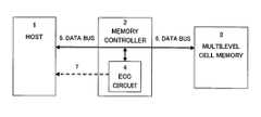
- FIG. 1is a view of the configuration of a memory system using a multilevel cell memory.
- the host 1 and the multilevel cell memory 3are connected by data buses 5 , 6 , between which a memory controller 2 is provided.
- a first data bus 5is provided between the host 1 and memory controller 2
- a second data bus 6is provided between the memory controller 2 and the multilevel cell memory 3 .
- the memory controller 2generates error correction codes (hereafter “ECC codes”) for data supplied by the data buses 5 , 6 , and incorporates an ECC circuit 4 which performs error correction.
- ECC codeserror correction codes
- the host 1reads data from, and writes data to, the multilevel cell memory 3 .
- the memory controller 2intermediates to enable the host 1 to access the multilevel cell memory 3 .
- the ECC circuitWhen the host 1 writes data to the multilevel cell memory 3 , the ECC circuit generates an ECC code for this data, and writes the ECC code, together with the data, to the multilevel cell memory 3 . Normally, this ECC code is written to spare area, which is a redundant cell area of the multilevel cell memory 3 .
- the ECC circuit 4when the host 1 reads data from the multilevel cell memory 3 , the ECC circuit 4 generates an ECC code for the read data, and by comparing the generated ECC code with the read-out ECC code, detects data errors and corrects these errors.
- the ECC circuit 4when the ECC circuit 4 detects a data error, the host is notified of the error occurrence by the error detection means 7 , and error correction information (the error occurrence address and similar) is transmitted to the host 1 via the data bus 5 . The host 1 then corrects the readout data error according to the error correction information.
- the ECC circuit 4incorporates a data buffer which holds, for example, one page worth of data; errors are corrected within the ECC circuit, and the corrected data is transmitted to the host 1 via the data bus 5 .
- the memory controller of this aspect of the embodimentmay have either of these configurations.
- FIG. 2is a circuit diagram showing an example of the configuration of a multilevel cell memory. This is an example of NAND-type flash memory. For simplicity, an example in which two bits of data are held in one cell is explained.
- cell strings in which a plurality of cells MC are connected in a columnare connected to the bit lines BL 0 , BL 1 , and word lines WL 0 , WL 1 are connected to the control gate for each cell.
- Each cell MChas, for example, a floating gate, and four charge states are stored in the floating gate. Hence each cell MC stores two bits of data.
- two page buffers PBare connected to each of the bit lines BL 0 , BL 1 , and when one cell MC is accessed, data is read one bit at a time to the two page buffers PB; in the other hand, the charge state of a single cell MC is stored according to the two bits of data input to the page buffers PB respectively.
- FIG. 3is a figure showing cell charge states.
- the vertical axisindicates the cell threshold voltage; the horizontal axis indicates the number of cells. That is, the distribution of the plurality of threshold voltages of a cell is shown.
- the charge states within the cell floating gateinclude the state of (0,1) data for which there is an extremely large amount of charge (electrons), and the threshold voltage is highest; the state of (0,0) data with the next-largest amount of charge and the next-highest threshold voltage; the state of (1,0) data with the next-largest amount of charge and the next-highest threshold voltage; and then the state of data (1,1). If the potential of the word line is set at a level between the threshold distributions, differences occur in the drain current of the cell transistor according to the state, and it is possible to detect the distribution charge state.
- FIG. 4is a view of the configuration of a multilevel cell memory device.
- the cell array for a single pageis shown; the cell array has a data area 8 for storage of data, and a spare area 9 having redundant cells for replacing ing of defective cells. ECC codes generated for the write data are written to this spare area 9 .
- four charge statescan be stored in each cell MC, and consequently two bits of data A, B can be stored.
- the data area 8has a capacity of 512 bytes
- the spare area 9has a capacity of 16 bytes. That is, the data capacity of one page is 512 bytes, and the corresponding spare area 9 has a capacity of 16 bytes.
- one word line WLWhen one word line WL is selected, 512 bits of data from the data area 8 , and 16 bits of data from the spare area 9 , for a total of 528 bits, are read to the page buffer, not shown.
- By simultaneous selection of eight word lines512 bytes of data are read from the data area 8 , and 16 bytes of data are read from the spare area 9 into the page buffer. Then, data is output 8 bits (one byte) at a time to eight I/O terminals, in synchronization with address increments.
- FIG. 5is a figure showing the page configuration of multilevel cell memory. Flash memory normally performs readout and write operations in page units. Hence the cell area has a plurality of pages. As shown in FIG. 4, each page has a 512-byte data area 8 and a 16-byte spare area 9 . In the example of FIG. 4, there are eight input/output terminals I/O. In the case of 16 input/output terminals I/O, each page consists of a 512-word data area 8 and a 16-word spare area 9 .
- the flash memoryis only instructed to perform reading or writing of a certain page by the memory controller. Hence in the specified page, the flash memory increments (or decrements) the address in synchronization with the clock in the memory, and performs address management within the page. That is, when there is a request to access a particular page, the flash memory first accesses the 512 bytes of data in the data area 8 while incrementing the address in the page, and then accesses the 16 bytes of data in the spare area 9 .
- a single page of datais divided into a plurality of data groups, and error correction codes capable of correction of single-bit defects are generated for each data group and are stored in the spare area in the memory device.
- bits of data associated with a single multilevel cellare then divided into a plurality of data groups without overlap, and correction of at most one error bit is possible for each of the divided data groups.
- the data of one pagecan be separated into the direction of input/output terminal (column direction) corresponding to the plurality of bits of the data bus, and the direction of address (row direction) assigned to the plurality of bits of the data bus.
- the data of one pageis accessed in word units while incrementing the address, so that if the data is divided in the input/output terminal direction (column direction), the plurality of data bits of the data bus are divided into a plurality of data groups within the data bus, and if divided in the address direction (row direction), the plurality of data bits of the data bus are divided into a plurality of data groups within a plurality of addresses.
- FIG. 6is a figure showing an example of the configuration of a memory device and memory controller, for the case in which page data is separated in input/output terminal (column) units into a plurality of ECC zones.
- the memory device 3is an example in which two bits of data are held in one cell MC, in a configuration enabling access of the eight bits of data in four cells at the same address Ai.
- Each of the two bits of data of each cellare separated into the lower input/output terminal groups I/O 0 to I/O 3 and the upper input/output terminal groups I/O 4 to I/O 7 , without overlap.
- the two bits of data of the cell MC shown in the figureare allocated, one to the input/output terminal I/O 0 , the other to the input/output terminal I/O 4 .
- the two bits of data of the other cellsare also allocated to I/O 1 and I/O 5 , I/O 2 and I/O 6 , and I/O 3 and I/O 7 , respectively.
- the four pairs of two data bits I/O 0 , 4 , I/O 1 , 5 , I/O 2 , 6 , I/O 3 , 7are connected to the eight input/output terminals I/O 0 to I/O 7 via the input/output wiring structure 40 in the memory device 3 , and the input/output terminals are connected to the second data bus 6 .
- the 512 bytes and 16 bytes of the data area 8 and the spare area 9be separated into at least two ECC zones in the input/output terminal (column) direction, and that ECC codes be generated for each. Even if one cell MC is defective and two data bits are error bits, the two data bits are separated into different ECC zones, for which separate ECC codes are generated; so that even if the ECC code is a code capable of correcting only a single bit, two ECC codes can be used to correct two data bits of one cell MC.
- the 8 bits of the first data bus 5are separated into the four lower bits DB 0 to 3 and the four upper bits DB 4 to 7 , and the respective data groups DB 0 to 3 and DB 4 to 7 are supplied to the ECC circuits 20 , 22 of zones 0 and 1 .
- ECC codesare generated for the respective supplied data groups DB 0 to 3 and DB 4 to 7 , and in addition the supplied data groups DB 0 to 3 and DB 4 to 7 are output without modification at the data output circuit 30 to the eight bus lines of the second data bus 6 , and supplied to the eight input/output terminals I/O 0 to 7 of the memory device 3 .
- one bit from the first data group I/O 0 to 3 and one bit from the second data group I/O 4 to 7are combined by the input/output wiring structure 40 , and four pairs of two data bits I/O 0 , 4 , I/O 1 , 5 , I/O 2 , 6 , I/O 3 , 7 , are written to four two-bit cells MC respectively.
- the ECC circuits 20 , 22complete generation of the respective ECC codes, and the generated first and second ECC codes are supplied to the input/output terminals I/O 0 to 3 and I/O 4 to 7 of the memory device, via the lower bits and upper bits of the second data bus 6 .
- two data bitsare written to cells of the spare area 9 , similarly to the data area 8 .
- the 512 bytes and 16 bytes of dataare read to a page buffer, not shown, and data held in the page buffer is output eight bits at a time to the input/output terminals I/O 0 to 7 by incrementing the address.
- the ECC circuits 20 , 22 within the memory controllergenerate ECC codes on input of the first and second data groups, and then compare the generated ECC codes with the first and second ECC codes read from the spare area 9 , and perform error detection and error correction.
- the data of the read-out first and second data groupsis transferred to the host 1 via the first data bus 5 , and error correction data is supplied to the host 1 via error notification means 7 , not shown.
- the two data bits associated with one two-level cellare separated into first and second data groups without overlap by the input/output wiring structure 40 in the memory device, and the first and second data groups are allocated to the lower input/output terminal group I/O 0 to 3 and to the upper input/output terminal group I/O 4 to 7 , respectively.
- the first and second ECC circuits 20 , 22generate the ECC codes for the input lower data group DB 0 to 3 and the upper data group DB 4 to 7 in the first data bus 5
- the data output means 30outputs the first and second data groups, and the first and second ECC codes, to the lower data group and upper data group of the second data bus 6 .
- FIG. 7is a figure showing another example of the configuration of a memory device and memory controller, for the case in which page data is separated in input/output terminal (column) units into a plurality of ECC zones.
- this memory devicethere is no input/output wiring structure 40 as in FIG. 6, and the input/output terminals are allocated two data bits per cell from the lowest data group, without modification. Otherwise the data area 8 and spare area 9 are the same as in FIG. 6. Hence in this case also, it is necessary to divide data into first and second data groups in the input/output terminal (column) direction.
- the configuration of the memory controller 2is the same as the example of FIG. 6.
- the plurality of data bits of the first data bus 5are separated into first and second ECC zones, and the ECC circuits 20 , 22 generate ECC codes for the data of the respective ECC zones.
- the data output means 30 of the memory controller 2then supplies the data DB 0 , DB 4 , DB 1 , DB 5 , DB 2 , DB 6 , DB 3 , DB 7 to the input/output terminals I/O 0 to 7 of the memory device 3 .
- FIG. 8is a figure showing an example of the configuration of a memory device and memory controller, for the case in which page data is separated in address (row) units into a plurality of ECC zones.
- this memory devicethe two data bits of a two-bit cell are output to the eight input/output terminals I/O 0 to 7 without overlap. That is, for a given address, one data bit each is output from eight cells to the eight input/output terminals I/O 0 to 7 .
- the data of one pagemust be separated in address (row) units.
- addressesare incremented starting from the lowest address A 0 , and so the ECC circuit 20 of the memory controller 2 inputs the 8 bits supplied from the first data bus 5 in order, generates a first ECC code for the first data group, associated with addresses A 0 to 3 , and generates a second ECC code for the second data group, associated with addresses A 4 to 7 .
- the first and second ECC codesare written in order to the spare area 9 .
- the ECC circuit 20 of the memory controller 2is provided for common use with the first and second ECC zones.
- an ECC holding circuitnot shown, is necessary in the ECC circuit 20 .
- the data output circuit 30 in the memory controller 2outputs the eight bits of data of the first data bus 5 without modification to the second data bus 6 , supplying them to the eight bits of the input/output terminals I/O 0 to 7 of the memory device 3 .
- FIG. 9is a figure showing another example of the configuration of a memory device and memory controller, for the case in which page data is separated in address (row) units into a plurality of ECC zones.
- the two bits of data of one cellare output without overlap to eight input/output terminals I/O 0 to 7 . That is, for a given address, one data bit from each of eight cells is output to eight input/output terminals I/O 0 to 7 .
- the data of one pagemust be separated in address (row) units.
- the even-numbered addresses A 0 , A 2 , A 4 , A 6are allocated to the first bit of four cells, and the odd-numbered addresses A 1 , A 3 , A 5 , A 7 are allocated to the second bit of the same four cells.
- ECC codescapable of correcting only single-bit errors can be used to correct the two data bit errors accompanying one defective cell.
- the memory controller 2has data input means 32 to supply the eight data bits DB 0 to 8 of the first data bus 5 , in order, to the first and second ECC circuits, and data output means 30 to output the eight data bits via the first and second ECC circuits and the ECC codes to the second data bus 6 .
- ECC circuitsare not used in common, but are provided for each of the first and second data groups.
- FIG. 10is a figure which explains write operations to multilevel cell memory.
- Write operationsare as follows. First, in order to write data to the multilevel cell memory 3 , the host 1 supplies a write destination address (page address) in the multilevel cell memory 3 and data to be written to the multilevel cell memory 3 to the memory controller 2 , via the first data bus 5 (step S 1 ). Then, the memory controller 2 supplies the write destination address (page address) in the multilevel cell memory 3 and the data for writing to the multilevel cell memory 3 , supplied by the host 1 , to the multilevel cell memory 3 , via the second data bus 6 .
- the ECC circuit 4In order that error detection and correction of this data can be performed at the time of reading of the data, the ECC circuit 4 generates an ECC code according to the data and supplies it to the multilevel cell memory 3 via the second data bus 6 (step S 2 ).
- the multilevel cell memory 3writes the data supplied by the memory controller 2 to the data area 8 of the multilevel cell memory 3 at the page corresponding to the write destination address, also supplied by the memory controller 2 , and then, in the redundant data area 9 , writes the ECC code generated based on the data (step S 3 ).
- FIG. 11is a figure which explains read operations from multilevel cell memory.
- the read operationis as follows.
- the host 1supplies a read address (page address) in the multilevel cell memory 3 to the memory controller 2 , via the first data bus 5 (step S 11 ).
- the memory controller 2supplies to the multilevel cell memory 3 , via the second data bus 6 , the read address of the multilevel cell memory 3 , supplied by the host 1 (step S 12 ).
- the multilevel cell memory 3reads, in order, the data in the data area 8 at the page corresponding to the read address supplied by the memory controller 2 , and the ECC code from the redundant data area 9 , and supplies these to the memory controller 2 via the second data bus 6 (step S 13 ).
- the memory controller 2supplies the readout data and ECC code, supplied by the multilevel cell memory 3 , to the ECC circuit 4 for the purpose of error detection and correction (step S 14 ).
- the readout datais also supplied to the host 1 via the first data bus 5 (step S 15 ).
- the ECC circuit 4performs error detection and correction of the readout data supplied by the memory controller 2 , based on the ECC code, and uses the error notification means 7 to notify the host of the result (step S 16 ). In cases where errors are detected and error correction is possible, the memory controller 2 notifies the position of the data bits to be corrected via the first data bus 5 .
- one page worth of datais stored temporarily in the data buffer, and the data and ECC code are used to detect the positions of data bits to be corrected, and to perform data correction.
- the corrected datais then supplied to the host 1 via the first data bus 5 . In this case, error notification is unnecessary.
- FIG. 12is a figure showing an example of division in input/output terminal (column) units.
- the data areas 8 of each page of the multilevel cell memory 3have a capacity of 512 words, and are divided into four zones Z 0 to Z 3 , with columns 0 to 3 , 4 to 7 , 8 to 11 , and 12 to 15 .
- bit numbersare allocated respectively to the 4 ⁇ 512 bits of data in each zone. These bit numbers (9 bits) comprise a combination of row numbers and column numbers (2 bits), in binary notation.
- the ECC codes in this exampleare capable of correcting one-bit errors, and, with the data divided into a pair of data groups having a “0” or “1” in each digit of the bit number, the ECC codes comprise the parity of all bits associated with each data group. That is, as shown in the lower part of FIG. 12, the pair of ECC codes lp00, lp01 has the parity lp00 (lp: line parity) of the data group in which the lowest bit of the row number of the bit number is “0”, and the parity lp01 of the data group in which the lowest bit of the row number is “1”.
- the next ECC code pair lp02, lp03has the parity lp02 of the data group in which the second-lowest bit of the row number of the bit number is “0”, and the parity lp03 of the data group in which the same bit is “1”.
- the ECC codescomprise pairs of parity for each digit of the bit number representing a row number.
- the ECC code generation circuitcounts the number of “1”s or “0”s in the supplied data, and depending on whether the result is even or odd, sets the ECC code to “1” or “0”.
- the ECC code generation circuitis realized by, for example, 22 flip-flop circuits which are inverted according to the supplied data. The supplied data is distributed to the 22 flip-flop circuits according to the bit numbers. The configuration will differ depending on whether odd parity or even parity is adopted.
- FIG. 13is a figure which explains storage of ECC codes in spare area.
- the spare area of the memory devicehas cells which replace defective cells and cells which store ECC codes, and has a 16-word capacity.
- the spare area 9is also divided into four zones Z 0 to Z 3 in the column direction.
- the ECC codes generated corresponding to each zoneare stored in each of the zones of the spare area 9 .
- FIG. 14is a figure showing an ECC circuit within a memory controller applied to the example of FIGS. 12 and 13. This example is the ECC circuit corresponding to FIG. 6.
- the first data bus 5 and second data bus 6have a 16-bit configuration. And because the 16 bits are divided among four zones, the ECC circuit also has a four-column configuration corresponding to the four zones.
- each data byte supplied by the host 1 via the first data bus 5is divided at each four bits, and supplied to the corresponding ECC code generation circuit 20 A to 26 A.
- each data byteis supplied to the memory device through the second data bus 6 , via the data output means 30 .
- Each of the ECC code generation circuits 20 A to 26 Acounts the data supplied, and generates the above-described parity code.
- An ECC control circuit 50provided within the memory controller, generates the internal clock CLK in synchronization with the system clock CLK; data supplied in synchronization with this clock CLK is transferred to the memory device, and the ECC code generation circuit performs a data counting operation.
- the ECC generation circuits 20 A to 26 Aend the generation of ECC codes for each zone.
- the ECC codesare supplied to the memory device from the data output means 30 via the second data bus 6 .
- the ECC code generated for each zoneis, like data divided into zones, output from the second data bus 6 , so that as explained in FIG. 13, the ECC codes are stored in the different zones of the spare area 9 within the memory device.
- each error detection and correction circuithas 22 exclusive OR logic circuits. Comparison of the ECC codes read from the spare area of the memory device and the ECC codes newly generated at the time of readout, that is, comparison of the parity of 11 pairs, is then performed. In the ECC code method of this example using parity pairs, error detection is performed as explained below using the result of an exclusive OR operation.
- the data error bitcan be determined from the 11 data groups in which non-coincidence has occurred.
- the bit number for correctionis, of the 22 exclusive OR results, the exclusive OR data of the odd-numbered ECC codes lp17, lp15, lp13, lp11, lp09, lp07, lp05, lp03, lp01, cp03, cp01.
- the bit number for correctionis the exclusive OR data of the even-numbered ECC codes.
- the error detection and correction circuitnotifies the host 1 of the result of an exclusive OR operation of the readout ECC codes and the ECC codes generated from the readout data, as the bit number of the data for which an error has occurred.
- N-bit error correction using the above error correction codeassumes high reliability of the memory device, and correction of errors in cases in which there are errors in at most a single N-level cell. If errors occur in a plurality of N-level cells, correction is not possible.
- FIG. 15is a figure showing an example of division in address (row) units.
- the data area 8 of each page of the multilevel cell memoryhas a capacity of 512 words, divided into four zones Z 0 to Z 3 , with addresses 0 to 127, 128 to 255, 256 to 383, and 384 to 511.
- bit numbersare allocated to the 16 ⁇ 128 bits of data in each zone. These bit numbers comprise combinations of row numbers (7 bits) and column numbers (4 bits), in binary notation.
- bit numbersare allocated for the data of zone Z 3 . That is, the row numbers are 0 to 127 and column numbers are 0 to 15, and each bit number is represented by 11 bits.
- FIG. 16is a figure showing an example of ECC codes generated for each zone.
- the ECC codes of this examplealso employ a method such that single-bit error can be corrected within a zone even with a small number of bits for ECC; in FIG. 15, the data in a zone is divided into “0” data groups and “1” data groups for each digit of the bit numbers assigned to the data.
- one pair of ECC codes lp00, lp00comprises a parity bit for the data group the lowest bit of the row number of which is “0”, and a parity bit for the data group the same bit of which is “1”.
- Other ECC codesare similar, and in total there are 11 pairs of parity bits.
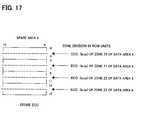
- FIG. 17is a figure which explains storage of generated ECC codes into the spare area.
- the 16-word spare area 9 allocated to each page of the N-level cell memoryis divided in four by address (row), and the ECC codes of zone Z 0 are stored in the spare area of addresses 0 to 3, the ECC codes of zone Z 1 are stored in the spare area of addresses 4 to 7, the ECC codes of zone Z 2 are stored in the spare area of addresses 8 to 11, and the ECC codes of zone Z 3 are stored in the spare area of addresses 12 to 15.
- FIG. 18is a figure showing an ECC circuit within a memory controller applied to the example of FIGS. 15 through 17. This example corresponds to the memory controller shown in FIG. 8.
- ECC circuit of FIG. 14for the case of division in the input/output terminal (column) direction, in FIG. 18 only one ECC circuit, comprising an ECC code generation circuit 20 A and error detection and correction circuit 22 A, is provided.
- ECC code holding means 54 , 56 , 58 to hold the ECC codes for the three ECC zones, and a selector circuit 52are also provided.
- the 512 words of data in the pageis separated into four zones, with the lower addresses 0 to 127, and the upper addresses 128 to 255, 256 to 382, and 383 to 511.
- the memory deviceincrements the internal address ADD in the page in synchronization with the system clock CLK.
- the 16-bit data of the lower addresses 0 to 127is first output, in order, to the first data bus 5 from the host 1 , and is transferred to the memory device from the output control circuit 30 via the second data bus 6 ; in addition, the lower-address data is supplied, in order, to the ECC code generation circuit 20 A.
- the ECC code generation circuit 20 Aconsists of, for example, 22 flip-flop circuits for II pairs of ECC, and data is distributed to the flip-flop circuits according to the address ADD. Hence at the time when transfer from the host 1 to the memory device 3 of the 512 words of data associated with the lower addresses 0 to 127 is ended, ECC code generation for this zone Z 0 is also ended, and the ECC codes are stored temporarily in the ECC code holding means 54 , via the selector 52 .
- the data of the subsequent addresses 128 to 255is similarly transferred, in order, from the host 1 to the memory device 3 in word units, and is also supplied to the ECC code generation circuit 20 A, to generate ECC codes for the zone Z 1 . After generation, the ECC codes are stored temporarily in the ECC code holding means 56 . The data of zones Z 2 and Z 3 is similarly transferred to the memory device 3 via the second data bus 6 , and the respective ECC codes are generated.
- the ECC codes of the zones Z 0 , Z 1 , and Z 2are stored in the holding means 54 , 56 , 58 respectively, and the ECC code generation circuit 20 A ends generation of the ECC codes for zone Z 3 . Then, in succession to the data, the ECC codes for the four zones are stored in the addresses 0 to 3, 4 to 7, 8 to 11, and 12 to 15, respectively in the spare area.
- the data of the page specified by the host 1is read, in order, according to the internal address ADD incremented in synchronization with the system clock CLK, and is supplied to the ECC code generation circuit 20 A, and is also transferred to the host 1 .
- the ECC codes for the zones Z 0 , Z 1 , Z 2are generated in order, and are stored in the ECC code holding means 54 , 56 , 58 , respectively.
- the ECC codes for zone Z 3are generated by the generation circuit 20 A, the ECC codes which had previously been generated and stored are read, in order, from the spare area of the memory device, and are supplied to the error detection and correction circuit 22 A.
- the error detection and correction circuit 22 Ahas 22 exclusive OR circuits corresponding to 11 pairs of ECC codes, and performs checks to determine whether there is coincidence between the ECC codes generated at the time of reading of each zone, and the ECC codes read from the spare area of the memory device.
- the ECC codes of this exampleare the same as in the previously described example, and the error detection method, and method of address generation of the bit for correction on occurrence of a one-bit error, are also the same.
- the error detection and correction circuit 22 Aperforms comparisons of ECC codes, in the order zone Z 0 , Z 1 , Z 2 , Z 3 , according to incrementing of the address.
- a memory controllercan be provided which generates ECC codes enabling error correction of the data of a multilevel cell memory, and which performs error detection and correction.
- the data of a multilevel cell memoryis separated, so that there is no overlap of the n bits of data associated with one multilevel cell, into first through Mth data groups (where M is greater than or equal to n), and first through Mth error correction codes are generated for these first through Mth data groups; hence even if a defect occurs in one multilevel cell, so that errors occur in n bits, correction of one bit each can be performed using the error correction codes for each data group, so that correction of n error bits is possible.
Landscapes
- Engineering & Computer Science (AREA)
- Theoretical Computer Science (AREA)
- Quality & Reliability (AREA)
- Physics & Mathematics (AREA)
- General Engineering & Computer Science (AREA)
- General Physics & Mathematics (AREA)
- For Increasing The Reliability Of Semiconductor Memories (AREA)
- Techniques For Improving Reliability Of Storages (AREA)
- Detection And Correction Of Errors (AREA)
- Read Only Memory (AREA)
- Error Detection And Correction (AREA)
Abstract
Description
- 1. Field of the Invention[0001]
- This invention relates to a memory controller for a multilevel cell memory, and in particular to a memory controller having an ECC circuit which generates error detection/correction codes and performs an error detection and correction for multilevel cells.[0002]
- 2. Description of the Related Art[0003]
- Flash memory is coming into widespread use primarily in portable data terminals, portable telephone sets, and other portable information equipment. Flash memory is nonvolatile semiconductor memory, which can retain stored data even if the power supply is turned off, and so is widely adopted mainly in battery-driven portable information equipment.[0004]
- Trends toward greater functionality and broadband communications in recent years have been accompanied by mounting demand for flash memory with greater storage capacity. In order to satisfy such demands, multilevel-cell flash memory has been proposed. Broadly defined, this multilevel-cell memory is memory in which cells store states with three or more values; normally, in this memory cells store 2[0005]nstates (where n is an integer greater than or equal to 2). Hence if there are four charge states, two bits of data are stored in a single cell; if there are eight charge states, three bits of data are stored in a single cell; and if there are 2ncharge states, then n bits of data are stored in a single cell.
- Semiconductor memory such as flash memory has a high per-bit cost, and therefore the use of ECC code, which requires numerous bits, is not suited to flash memory. On the other hand, flash memory is more reliable than hard disks or other storage media, with a defect occurring in at most one cell. Hence many conventional one-bit-cell memory devices adopt as the ECC code a Hamming code, for which correction of up to one-bit errors is possible. This is because, for an ECC code capable of correction of errors in a plurality of bits, the number of bits required to the ECC becomes too great, and there is no need for correction of errors in a plurality of bits. That is, when, as in the case of flash memory, the per-bit cost is high, but reliability is high enough that a defect occurs in at most one bit, a Hamming code enabling correction of up to one bit error using a small number of bits is appropriate as the ECC code.[0006]
- If a defect occurs in a certain cell of a multilevel cell memory supporting large storage capacity, the n bits of data associated with the defective cell may simultaneously become defective bits. Consequently an error correction code using the above Hamming code capable of correction of up to one-bit errors cannot correct the errors in n bits (where n is two or greater) accompanying a single defective cell, and so a different type of ECC code other than the Hamming code, with a greater number of bits, must be used. For example, a complex ECC code adopted in hard disks might be used. However, such ECC codes with a large number of bits are not suited to flash memory with its high per-bit cost.[0007]
- In order to address the above problem, it has been proposed, in U.S. Pat. No. 5,754,566, that an ECC circuit be provided in a memory device, that this ECC circuit be designed to separate serial data into a plurality of data words, so that within a data word there is only one bit associated with the n bits of one cell, and that an ECC code be generated for each data word, and stored in an n-bit cell.[0008]
- However, incorporation of an ECC circuit in a memory device will tend to increase the cost of the memory device, and so is undesirable. Particularly in a system in which are installed a plurality of memory devices, the same ECC circuit is provided redundantly in a plurality of memory devices, driving up the cost of the overall system.[0009]
- An object of the present invention is to provide a memory controller which incorporates an ECC circuit for a multi-bit cell memory.[0010]
- A further object of this invention is to provide a memory controller which, for a multi level cell memory, generates an ECC code capable of error correction using a small number of bits, and performs error correction.[0011]
- In order to achieve the above objects, a first aspect of this invention is a memory controller for a multilevel cell memory, connected between a host and an N-level cell memory (where N=2[0012]n, and n is an integer greater than or equal to 2) via data buses the widths of each of which are a plurality of bits, comprising: first through Mth ECC circuits (where M is equal to n or greater), which input in parallel first through Mth data groups of a first data bus connected to the host, and generates first through Mth error correction codes capable of correction single-bit defect, for the first through Mth data groups; and data output unit which outputs the data groups to a second data bus connected to the data input/output terminals of the above N-level cell memory, such that the n-bit data associated with a single N-level cell are separated into the first through Mth data groups without overlap; and wherein the data output unit further outputs to the second data bus the error correction codes generated by the above ECC circuits.
- Of the plurality of bits of data input via the second data bus, the N-level cell memory connected to the above memory controller for multilevel cell memories combines at most single bit of data from each of the first through Mth data groups, and stores these combined data bits in a single N-level cell. It is preferable that at most the single bit of data from each of the error correction codes generated by the first through Mth ECC circuits also be combined and stored in a single N-level cell.[0013]
- The N-level cell memory controlled by the memory controller of the above invention have an internal configuration in which the plurality of data input/output terminals connected to the second data bus are separated into first through Mth data input/output terminal groups, such that there is no redundancy in the n bits of data associated with one N-level cell. Together with this, the memory controller separates the plurality of data bits on the first data bus into first through Mth data groups, the ECC circuits generate error-correction codes for each of these data groups, and the first through Mth data groups and first through Mth error correction codes are input to the first through Mth data input/output terminals of the N-level cell memory, via the second data bus.[0014]
- As a result, the n bits of data associated with each N-level cell are separated into a plurality of ECC zones without overlap, and error-correction codes are generated and stored for the data of each of the ECC zones. Hence even if a defect occurs in one N-level cell, and n bits of data become defective simultaneously, the error-correction codes generated for each ECC zone can be used to perform correction of the n bits of data. That is, n defective bits can be corrected even when using an error correction code capable of correction of a single defective bit.[0015]
- When the data input/output terminals of an N-level cell memory device are separated into, in order from the lowest, first, second, . . . , Mth data groups, the data output unit of the memory controller outputs data to the second data bus so as to be allocated, in order from the lowest, to the first, second, . . . , Mth data groups. Together with this, the data of the first data bus can also be divided, in order from the lowest, into first, second, . . . , Mth data groups, and input to the first through Mth ECC circuits, so that the configuration for division into data groups within the memory controller is comparatively simple.[0016]
- When the data input/output terminals of an N-level cell memory device are divided into data groups associated with N-level cells in order from the lowest, the memory controller data output unit outputs data to the second data bus such that data for the first, second, . . . , Mth data groups, in order from the lowest, is repeated cyclically. That is, the data output unit combines data from the first through Mth data groups for output to the second data bus, such that the n bits of data associated with one N-level cell are divided into the first through Mth data groups, without overlap.[0017]
- In the above invention, when reading data from N-level cell memory, the first through Mth data groups and the first through Mth error correction codes of the second data bus, are provided to the respective first through Mth ECC circuits within the memory controller, and the first through Mth ECC circuits perform one-bit error correction within the first through Mth data groups.[0018]
- Hence between the host and the N-level cell memory, writing is performed via the first data bus, first through Mth ECC circuits, data output unit, and second data bus; and reading is performed via the same route, but in the opposite order.[0019]
- Write data is supplied to the ECC circuits and is provided to the memory in synchronization with the clock; in addition, read data is output from the memory and supplied to the ECC circuits in synchronization with the clock. Hence the effect on clock synchronization operation between the host and the memory device can be minimized, and error correction code generation and error correction can be performed.[0020]
- In order to attain the above objects, a second aspect of this invention is a memory controller for a multilevel cell memory, connected between a host and an N-level cell memory (where N=2[0021]n, and n is an integer greater than or equal to 2) via data buses the widths of each of which are a plurality of bits, comprising: a common ECC circuit which inputs in order first through Mth (where M is greater than or equal to n) data groups, separated in the address direction, for the data groups of the first data bus, connected to the host, and generates first through Mth error correction codes capable of correction of single-bit defect for the first through Mth data groups; error correction code holding unit to hold the first through the (M−1)th error correction codes; and data output unit to output the data to the second data bus, connected to the above N-level cell memory, such that the n bits of data associated with a single N-level cell are separated into the first through Mth data groups without overlap; and wherein the data output unit outputs to the second data bus the first through (M−1)th error correction codes held by the error correction code holding unit and the Mth error correction code generated by the above ECC circuit.
- In order to attain the above objects, a third aspect of this invention is a memory controller for a multilevel cell memory, connected between a host and an N-level cell memory (where N=2[0022]n, and n is an integer greater than or equal to 2) via data buses the widths of each of which are a plurality of bits, comprising: having first through Mth ECC circuits (where M is greater than or equal to n), which input first through Mth data groups, separated in the address direction, for the data group of the first data bus connected to the host, and for the first through Mth data groups, generate first through Mth error correction codes capable of correcting single-bit defects; data output unit which outputs data to the second data bus connected to the above N-level cell memory, such that the n bits of data associated with one N-level cell are separated into the first through Mth data groups without overlap; and wherein the data output unit outputs to the second data bus the error correction codes generated by the ECC circuits.
- In a more preferred embodiment, in the above first, second and third aspects of the invention, the memory device performs reading and writing of the plurality of data bits of the above data buses in page units each of which includes a plurality sets of plural bits data of the data bus, and the plurality of bits of data of the data bus are written to and read from an internal page buffer in internal address order. Further, the data within the page is separated into first through Mth data groups by (1) data input/output terminals (columns), or by (2) internal addresses (rows); error correction codes capable of single-bit error correction are generated by an ECC circuit for each data group, and correction is performed. Hence the ECC circuits and data output unit of the memory controller have a configuration compatible with the above separation method.[0023]
- In the above-described invention, the ECC generation circuits generate ECC codes based on an error correction code method capable of correction of single-bit defect for the data in each ECC zone. Hence the number of bits of the generated ECC code is held to a minimum, and can be stored in the spare area of flash memory. Thus only one of the bits of the n bits of data associated with a single N-level cell is associated with each ECC zone, so that even if defects occur in n bits due to occurrence of a defect in a single multilevel cell, correction of n error bits is possible, by performing single-bit error correction in each ECC zone.[0024]
- FIG. 1 is a view of the configuration of a memory system using a multilevel cell memory;[0025]
- FIG. 2 is a circuit diagram showing an example of the configuration of a multilevel cell memory;[0026]
- FIG. 3 is a figure showing cell charge states;[0027]
- FIG. 4 is a view of the configuration of a multilevel cell memory device;[0028]
- FIG. 5 is a figure showing the page configuration of multilevel cell memory;[0029]
- FIG. 6 is a figure showing an example of the configuration of a memory device and memory controller, for the case in which page data is separated in input/output terminal (column) units into a plurality of ECC zones;[0030]
- FIG. 7 is a figure showing another example of the configuration of a memory device and memory controller, for the case in which page data is separated in input/output terminal (column) units into a plurality of ECC zones;[0031]
- FIG. 8 is a figure showing an example of the configuration of a memory device and memory controller, for the case in which page data is separated in address (row) units into a plurality of ECC zones;[0032]
- FIG. 9 is a figure showing another example of the configuration of a memory device and memory controller, for the case in which page data is separated in address (row) units into a plurality of ECC zones;[0033]
- FIG. 10 is a figure which explains write operations to multilevel cell memory;[0034]
- FIG. 11 is a figure which explains read operations from multilevel cell memory;[0035]
- FIG. 12 is a figure showing an example of division in input/output terminal (column) units;[0036]
- FIG. 13 is a figure which explains storage of ECC codes in spare area;[0037]
- FIG. 14 is a figure showing an ECC circuit within a memory controller applied to the example of FIGS. 12 and 13;[0038]
- FIG. 15 is a figure showing an example of division in address (row) units;[0039]
- FIG. 16 is a figure showing an example of ECC codes generated for each zone;[0040]
- FIG. 17 is a figure which explains storage of generated ECC codes into storage area; and,[0041]
- FIG. 18 is a figure showing an ECC circuit within a memory controller applied to the example of FIGS. 15 through 17.[0042]
- Below, aspects of embodiments are explained, referring to the drawings. However, the scope of protection of this patent is not limited to the following aspects, but extends to the invention as described in the scope of claims, and the equivalent thereof.[0043]
- FIG. 1 is a view of the configuration of a memory system using a multilevel cell memory. Here a multilevel cell memory is memory capable of holding n bits (where n is an integer greater than or equal to 2) within a single cell; hence a single cell has N=2[0044]nstates. In this example, the
host 1 and themultilevel cell memory 3 are connected bydata buses memory controller 2 is provided. Specifically, afirst data bus 5 is provided between thehost 1 andmemory controller 2, and asecond data bus 6 is provided between thememory controller 2 and themultilevel cell memory 3. Thememory controller 2 generates error correction codes (hereafter “ECC codes”) for data supplied by thedata buses ECC circuit 4 which performs error correction. - The[0045]
host 1 reads data from, and writes data to, themultilevel cell memory 3. Here thememory controller 2 intermediates to enable thehost 1 to access themultilevel cell memory 3. When thehost 1 writes data to themultilevel cell memory 3, the ECC circuit generates an ECC code for this data, and writes the ECC code, together with the data, to themultilevel cell memory 3. Normally, this ECC code is written to spare area, which is a redundant cell area of themultilevel cell memory 3. And when thehost 1 reads data from themultilevel cell memory 3, theECC circuit 4 generates an ECC code for the read data, and by comparing the generated ECC code with the read-out ECC code, detects data errors and corrects these errors. - In the memory system example of FIG. 1, when the[0046]
ECC circuit 4 detects a data error, the host is notified of the error occurrence by the error detection means7, and error correction information (the error occurrence address and similar) is transmitted to thehost 1 via thedata bus 5. Thehost 1 then corrects the readout data error according to the error correction information. In another memory system example, theECC circuit 4 incorporates a data buffer which holds, for example, one page worth of data; errors are corrected within the ECC circuit, and the corrected data is transmitted to thehost 1 via thedata bus 5. The memory controller of this aspect of the embodiment may have either of these configurations. - FIG. 2 is a circuit diagram showing an example of the configuration of a multilevel cell memory. This is an example of NAND-type flash memory. For simplicity, an example in which two bits of data are held in one cell is explained. In the multilevel cell memory of FIG. 2, cell strings in which a plurality of cells MC are connected in a column are connected to the bit lines BL[0047]0, BL1, and word lines WL0, WL1 are connected to the control gate for each cell. Each cell MC has, for example, a floating gate, and four charge states are stored in the floating gate. Hence each cell MC stores two bits of data.
- Accompanying this, two page buffers PB are connected to each of the bit lines BL[0048]0, BL1, and when one cell MC is accessed, data is read one bit at a time to the two page buffers PB; in the other hand, the charge state of a single cell MC is stored according to the two bits of data input to the page buffers PB respectively.
- During readout, by selecting a word line, the data is read out to all page buffers PB, and one page of data is held. Data within the page buffer PB is output from the input/[0049]
output circuit 10 in units of the number of bits of the data bus, in response to a select signal, not shown. During writing, on the other hand, data is supplied from the data bus in units of the number of bits of the data bus, and is stored in the page buffers in response to a select signal, not shown; then cells MC are programmed to a charge state corresponding to the data. - FIG. 3 is a figure showing cell charge states. The vertical axis indicates the cell threshold voltage; the horizontal axis indicates the number of cells. That is, the distribution of the plurality of threshold voltages of a cell is shown. As shown in the figure, the charge states within the cell floating gate include the state of (0,1) data for which there is an extremely large amount of charge (electrons), and the threshold voltage is highest; the state of (0,0) data with the next-largest amount of charge and the next-highest threshold voltage; the state of (1,0) data with the next-largest amount of charge and the next-highest threshold voltage; and then the state of data (1,1). If the potential of the word line is set at a level between the threshold distributions, differences occur in the drain current of the cell transistor according to the state, and it is possible to detect the distribution charge state.[0050]
- FIG. 4 is a view of the configuration of a multilevel cell memory device. In FIG. 4, the cell array for a single page is shown; the cell array has a[0051]
data area 8 for storage of data, and aspare area 9 having redundant cells for replacing ing of defective cells. ECC codes generated for the write data are written to thisspare area 9. As shown in FIG. 4, four charge states can be stored in each cell MC, and consequently two bits of data A, B can be stored. - In the example of FIG. 4, in one page, the[0052]
data area 8 has a capacity of 512 bytes, and thespare area 9 has a capacity of 16 bytes. That is, the data capacity of one page is 512 bytes, and the correspondingspare area 9 has a capacity of 16 bytes. When one word line WL is selected, 512 bits of data from thedata area spare area 9, for a total of 528 bits, are read to the page buffer, not shown. By simultaneous selection of eight word lines, 512 bytes of data are read from thedata area spare area 9 into the page buffer. Then, data isoutput 8 bits (one byte) at a time to eight I/O terminals, in synchronization with address increments. - FIG. 5 is a figure showing the page configuration of multilevel cell memory. Flash memory normally performs readout and write operations in page units. Hence the cell area has a plurality of pages. As shown in FIG. 4, each page has a 512-[0053]
byte data area 8 and a 16-bytespare area 9. In the example of FIG. 4, there are eight input/output terminals I/O. In the case of 16 input/output terminals I/O, each page consists of a 512-word data area 8 and a 16-wordspare area 9. - The flash memory is only instructed to perform reading or writing of a certain page by the memory controller. Hence in the specified page, the flash memory increments (or decrements) the address in synchronization with the clock in the memory, and performs address management within the page. That is, when there is a request to access a particular page, the flash memory first accesses the 512 bytes of data in the[0054]
data area 8 while incrementing the address in the page, and then accesses the 16 bytes of data in thespare area 9. - In an N-level cell memory (where N is 4 or greater), a single cell stores n bits of data (2[0055]n=N). Specifically, n bits of data are stored by holding the 2nstates shown in FIG. 3 in a single cell. Hence when a single defective cell occurs within one page, errors occur simultaneously for n bits of data. In order to enable recovery from such data errors in a plurality of bits by using an error correction code capable of correcting single-bit defects, in this aspect, a single page of data is divided into a plurality of data groups, and error correction codes capable of correction of single-bit defects are generated for each data group and are stored in the spare area in the memory device. The n bits of data associated with a single multilevel cell are then divided into a plurality of data groups without overlap, and correction of at most one error bit is possible for each of the divided data groups. By this means, even if a single cell defect occurs, there is at most only one error bit in each of the data groups, so that even a simple error correction code capable of correcting only single-bit defects can be used for error correction of the defect of a multilevel cell.
- As described above, the data of one page can be separated into the direction of input/output terminal (column direction) corresponding to the plurality of bits of the data bus, and the direction of address (row direction) assigned to the plurality of bits of the data bus. The data of one page is accessed in word units while incrementing the address, so that if the data is divided in the input/output terminal direction (column direction), the plurality of data bits of the data bus are divided into a plurality of data groups within the data bus, and if divided in the address direction (row direction), the plurality of data bits of the data bus are divided into a plurality of data groups within a plurality of addresses.[0056]
- FIG. 6 is a figure showing an example of the configuration of a memory device and memory controller, for the case in which page data is separated in input/output terminal (column) units into a plurality of ECC zones. In this example, the[0057]
memory device 3 is an example in which two bits of data are held in one cell MC, in a configuration enabling access of the eight bits of data in four cells at the same address Ai. Each of the two bits of data of each cell are separated into the lower input/output terminal groups I/O0 to I/O3 and the upper input/output terminal groups I/O4 to I/O7, without overlap. That is, the two bits of data of the cell MC shown in the figure are allocated, one to the input/output terminal I/O0, the other to the input/output terminal I/O4. The two bits of data of the other cells are also allocated to I/O1 and I/O5, I/O2 and I/O6, and I/O3 and I/O7, respectively. The four pairs of two data bits I/O0,4, I/O1,5, I/O2,6, I/O3,7 are connected to the eight input/output terminals I/O0 to I/O7 via the input/output wiring structure 40 in thememory device 3, and the input/output terminals are connected to thesecond data bus 6. - In the case of the configuration of the[0058]
above memory device 3, it is necessary that the 512 bytes and 16 bytes of thedata area 8 and thespare area 9 be separated into at least two ECC zones in the input/output terminal (column) direction, and that ECC codes be generated for each. Even if one cell MC is defective and two data bits are error bits, the two data bits are separated into different ECC zones, for which separate ECC codes are generated; so that even if the ECC code is a code capable of correcting only a single bit, two ECC codes can be used to correct two data bits of one cell MC. - Together with this memory device structure, in the[0059]
memory controller 2 of this aspect, the 8 bits of thefirst data bus 5 are separated into the four lower bits DB0 to3 and the four upper bits DB4 to7, and the respective data groups DB0 to3 and DB4 to7 are supplied to theECC circuits zones ECC circuits data output circuit 30 to the eight bus lines of thesecond data bus 6, and supplied to the eight input/output terminals I/O0 to7 of thememory device 3. - In the[0060]
memory device 3, one bit from the first data group I/O0 to3 and one bit from the second data group I/O4 to7 are combined by the input/output wiring structure 40, and four pairs of two data bits I/O0,4, I/O1,5, I/O2,6, I/O3,7, are written to four two-bit cells MC respectively. - When 512 bytes of data are written to the[0061]
data area 8 of thememory device 3, theECC circuits second data bus 6. Within the memory device, two data bits are written to cells of thespare area 9, similarly to thedata area 8. - On the other hand, during a read operation in the[0062]
memory device 3, the 512 bytes and 16 bytes of data are read to a page buffer, not shown, and data held in the page buffer is output eight bits at a time to the input/output terminals I/O0 to7 by incrementing the address. TheECC circuits spare area 9, and perform error detection and error correction. - The data of the read-out first and second data groups is transferred to the[0063]
host 1 via thefirst data bus 5, and error correction data is supplied to thehost 1 via error notification means7, not shown. - In the example of FIG. 6, the two data bits associated with one two-level cell are separated into first and second data groups without overlap by the input/[0064]
output wiring structure 40 in the memory device, and the first and second data groups are allocated to the lower input/output terminal group I/O0 to3 and to the upper input/output terminal group I/O4 to7, respectively. Hence in thememory controller 2, the first andsecond ECC circuits first data bus 5, and the data output means30 outputs the first and second data groups, and the first and second ECC codes, to the lower data group and upper data group of thesecond data bus 6. - FIG. 7 is a figure showing another example of the configuration of a memory device and memory controller, for the case in which page data is separated in input/output terminal (column) units into a plurality of ECC zones. In this memory device, there is no input/[0065]
output wiring structure 40 as in FIG. 6, and the input/output terminals are allocated two data bits per cell from the lowest data group, without modification. Otherwise thedata area 8 andspare area 9 are the same as in FIG. 6. Hence in this case also, it is necessary to divide data into first and second data groups in the input/output terminal (column) direction. - There is no input/[0066]
output wiring structure 40 in thememory device 3, and so in the data output means30 of thememory controller 2, the lower or first data group DB0 to3 and the upper or second data group DB4 to7 in thefirst data bus 5 are interleaved, and one data bit each from the first and second data groups is output to thesecond data bus 6, arranged in alternation. That is, the data output means30 is provided with the function of the input/output wiring structure 40 of FIG. 6. As a result, two data bits consisting of one data bit each from the first and second data groups are written to each two-bits cell MC. Moreover, the first and second error correction codes (ECC codes) generated by the two ECC circuits are similarly written to two-bit cells in thespare area 9. - Otherwise, the configuration of the[0067]
memory controller 2 is the same as the example of FIG. 6. Hence the plurality of data bits of thefirst data bus 5 are separated into first and second ECC zones, and theECC circuits memory controller 2 then supplies the data DB0, DB4, DB1, DB5, DB2, DB6, DB3, DB7 to the input/output terminals I/O0 to7 of thememory device 3. As a result, four pairs of data, DB0 and DB4, DB1 and DB5, DB2 and DB6, and DB3 and DB7, are written to four two-bit cells. A similar operation is performed for ECC codes. During readout, data is read in the opposite order; in thememory controller 2, the ECC codes generated for the respective data groups are compared with the ECC codes read from thespare area 9, and error detection and error correction are performed. - FIG. 8 is a figure showing an example of the configuration of a memory device and memory controller, for the case in which page data is separated in address (row) units into a plurality of ECC zones. As opposed to the cases of FIG. 6 and FIG. 7, in this memory device the two data bits of a two-bit cell are output to the eight input/output terminals I/O[0068]0 to7 without overlap. That is, for a given address, one data bit each is output from eight cells to the eight input/output terminals I/O0 to7. Hence in order to separate the two data bits associated with a single cell into a plurality of ECC zones, the data of one page must be separated in address (row) units.
- In the[0069]
memory device 3 of FIG. 8 (if it is assumed that thedata area 8 has eight bytes of data with addresses A0 to7), the lower addresses A0, A1, A2, A3 are allocated to the first bit of four cells, and the upper addresses A4, A5, A6, A7 are allocated to the second bit of the same four cells. Hence in this case, by separating one page of data into lower addresses A0 to3 and upper addresses A4 to7, and generating ECC codes for each, even ECC codes capable of correcting only single-bit errors can be used to correct the two data bit errors accompanying one defective cell. - In this case, addresses are incremented starting from the lowest address A[0070]0, and so the
ECC circuit 20 of thememory controller 2 inputs the 8 bits supplied from thefirst data bus 5 in order, generates a first ECC code for the first data group, associated with addresses A0 to3, and generates a second ECC code for the second data group, associated with addresses A4 to7. After writing the data of addresses A0 to7 to thedata area 8, the first and second ECC codes are written in order to thespare area 9. - Hence the[0071]
ECC circuit 20 of thememory controller 2 is provided for common use with the first and second ECC zones. However, an ECC holding circuit, not shown, is necessary in theECC circuit 20. Thedata output circuit 30 in thememory controller 2 outputs the eight bits of data of thefirst data bus 5 without modification to thesecond data bus 6, supplying them to the eight bits of the input/output terminals I/O0 to7 of thememory device 3. - FIG. 9 is a figure showing another example of the configuration of a memory device and memory controller, for the case in which page data is separated in address (row) units into a plurality of ECC zones. In this example also, in the[0072]
memory device 3, the two bits of data of one cell are output without overlap to eight input/output terminals I/O0 to7. That is, for a given address, one data bit from each of eight cells is output to eight input/output terminals I/O0 to7. Hence in order to separate the two data bits associated with a single cell into a plurality of ECC zones, the data of one page must be separated in address (row) units. - Specifically, in the memory device[0073]3 (if it is assumed that the
data area 8 has eight bytes of data with addresses A0 to7), the even-numbered addresses A0, A2, A4, A6 are allocated to the first bit of four cells, and the odd-numbered addresses A1, A3, A5, A7 are allocated to the second bit of the same four cells. Hence in this case, by separating one page of data into odd-numbered and even-numbered addresses and generating ECC codes for each, even ECC codes capable of correcting only single-bit errors can be used to correct the two data bit errors accompanying one defective cell. - In the case of such a memory device, the[0074]
memory controller 2 has data input means32 to supply the eight data bits DB0 to8 of thefirst data bus 5, in order, to the first and second ECC circuits, and data output means30 to output the eight data bits via the first and second ECC circuits and the ECC codes to thesecond data bus 6. ECC circuits are not used in common, but are provided for each of the first and second data groups. - FIG. 10 is a figure which explains write operations to multilevel cell memory. Write operations are as follows. First, in order to write data to the[0075]
multilevel cell memory 3, thehost 1 supplies a write destination address (page address) in themultilevel cell memory 3 and data to be written to themultilevel cell memory 3 to thememory controller 2, via the first data bus5 (step S1). Then, thememory controller 2 supplies the write destination address (page address) in themultilevel cell memory 3 and the data for writing to themultilevel cell memory 3, supplied by thehost 1, to themultilevel cell memory 3, via thesecond data bus 6. In order that error detection and correction of this data can be performed at the time of reading of the data, theECC circuit 4 generates an ECC code according to the data and supplies it to themultilevel cell memory 3 via the second data bus6 (step S2). Next, themultilevel cell memory 3 writes the data supplied by thememory controller 2 to thedata area 8 of themultilevel cell memory 3 at the page corresponding to the write destination address, also supplied by thememory controller 2, and then, in theredundant data area 9, writes the ECC code generated based on the data (step S3). - The above supply of data for writing and ECC data to the[0076]
multilevel cell memory 3 is performed in synchronization with the system clock; the data for writing and ECC data are stored in the page buffer corresponding to the address within themultilevel cell memory 3, which is incremented in synchronization with the clock. - FIG. 11 is a figure which explains read operations from multilevel cell memory. The read operation is as follows. In order to read data from the[0077]
multilevel cell memory 3, thehost 1 supplies a read address (page address) in themultilevel cell memory 3 to thememory controller 2, via the first data bus5 (step S11). Next, thememory controller 2 supplies to themultilevel cell memory 3, via thesecond data bus 6, the read address of themultilevel cell memory 3, supplied by the host1 (step S12). - Next, the[0078]
multilevel cell memory 3 reads, in order, the data in thedata area 8 at the page corresponding to the read address supplied by thememory controller 2, and the ECC code from theredundant data area 9, and supplies these to thememory controller 2 via the second data bus6 (step S13). - The[0079]
memory controller 2 supplies the readout data and ECC code, supplied by themultilevel cell memory 3, to theECC circuit 4 for the purpose of error detection and correction (step S14). The readout data is also supplied to thehost 1 via the first data bus5 (step S15). - The[0080]
ECC circuit 4 performs error detection and correction of the readout data supplied by thememory controller 2, based on the ECC code, and uses the error notification means7 to notify the host of the result (step S16). In cases where errors are detected and error correction is possible, thememory controller 2 notifies the position of the data bits to be corrected via thefirst data bus 5. - Or, in cases where the[0081]
ECC circuit 4 has a one-page internal data buffer, one page worth of data is stored temporarily in the data buffer, and the data and ECC code are used to detect the positions of data bits to be corrected, and to perform data correction. The corrected data is then supplied to thehost 1 via thefirst data bus 5. In this case, error notification is unnecessary. - Next, an example of division in input/output terminal (column) units, and an example of division in address (row) units, are explained in detail, including the specific ECC method.[0082]
- Example of Division in Input/Output Terminal (Column) Units[0083]
- FIG. 12 is a figure showing an example of division in input/output terminal (column) units. In this example, as shown in the upper part of FIG. 12, the[0084]
data areas 8 of each page of themultilevel cell memory 3 have a capacity of 512 words, and are divided into four zones Z0 to Z3, withcolumns 0 to3,4 to7,8 to11, and12 to15. As shown in the middle part of FIG. 12, bit numbers are allocated respectively to the 4×512 bits of data in each zone. These bit numbers (9 bits) comprise a combination of row numbers and column numbers (2 bits), in binary notation. - The ECC codes in this example are capable of correcting one-bit errors, and, with the data divided into a pair of data groups having a “0” or “1” in each digit of the bit number, the ECC codes comprise the parity of all bits associated with each data group. That is, as shown in the lower part of FIG. 12, the pair of ECC codes lp00, lp01 has the parity lp00 (lp: line parity) of the data group in which the lowest bit of the row number of the bit number is “0”, and the parity lp01 of the data group in which the lowest bit of the row number is “1”. The next ECC code pair lp02, lp03 has the parity lp02 of the data group in which the second-lowest bit of the row number of the bit number is “0”, and the parity lp03 of the data group in which the same bit is “1”. Similarly, the ECC codes comprise pairs of parity for each digit of the bit number representing a row number.[0085]
- In the same way, for the two digits of column numbers of the bit number also, there are two pairs of ECC codes cp01 to cp03 (cp: column parity) comprising the parity of data groups having “0” and “1” as the column number digits. The bit number for the data of one ECC zone comprises 11 digits, so that if ECC codes are generated from a parity pair for each digit, a total of 22 ECC code bits are generated.[0086]
- In this ECC code method, the 512×4 bits of data in an ECC zone are divided into two using 11 different division methods, and the parity of all the data bits divided in each way is generated. Hence the ECC code generation circuit counts the number of “1”s or “0”s in the supplied data, and depending on whether the result is even or odd, sets the ECC code to “1” or “0”. The ECC code generation circuit is realized by, for example, 22 flip-flop circuits which are inverted according to the supplied data. The supplied data is distributed to the 22 flip-flop circuits according to the bit numbers. The configuration will differ depending on whether odd parity or even parity is adopted.[0087]
- FIG. 13 is a figure which explains storage of ECC codes in spare area. The spare area of the memory device has cells which replace defective cells and cells which store ECC codes, and has a 16-word capacity. As the data in a page is divided into four in the column direction, the[0088]
spare area 9 is also divided into four zones Z0 to Z3 in the column direction. The ECC codes generated corresponding to each zone are stored in each of the zones of thespare area 9. - FIG. 14 is a figure showing an ECC circuit within a memory controller applied to the example of FIGS. 12 and 13. This example is the ECC circuit corresponding to FIG. 6. In the example of FIGS. 12 and 13, as each page consists of 512 bytes of data, the[0089]
first data bus 5 andsecond data bus 6 have a 16-bit configuration. And because the 16 bits are divided among four zones, the ECC circuit also has a four-column configuration corresponding to the four zones. - As explained in FIG. 12, each data byte supplied by the[0090]
host 1 via thefirst data bus 5 is divided at each four bits, and supplied to the corresponding ECCcode generation circuit 20A to26A. At the same time, each data byte is supplied to the memory device through thesecond data bus 6, via the data output means30. Each of the ECCcode generation circuits 20A to26A counts the data supplied, and generates the above-described parity code. - An[0091]
ECC control circuit 50, provided within the memory controller, generates the internal clock CLK in synchronization with the system clock CLK; data supplied in synchronization with this clock CLK is transferred to the memory device, and the ECC code generation circuit performs a data counting operation. - At the point when 512 bytes of data have been supplied, the[0092]
ECC generation circuits 20A to26A end the generation of ECC codes for each zone. Hence in succession to the data, the ECC codes are supplied to the memory device from the data output means30 via thesecond data bus 6. The ECC code generated for each zone is, like data divided into zones, output from thesecond data bus 6, so that as explained in FIG. 13, the ECC codes are stored in the different zones of thespare area 9 within the memory device. - At the time of a readout operation, 512 bytes of data are read from the[0093]
data area 8 in the memory device, and are supplied to the memory controller from thesecond data bus 6. Data is transferred by the data output means30 in the opposite direction, 16 bits of readout data are divided into four zones, and are supplied to the corresponding ECCcode generation circuits 20A to26A. Simultaneously with this, the readout data is supplied to thehost 1 via thefirst data bus 5. - When readout of the 512 bytes of data ends, generation of the corresponding ECC codes by each of the ECC[0094]
code generation circuits 20A to26A also ends. If at most one bit error occurs in the readout data in each ECC zone, the ECC codes generated at the time of readout differ from the ECC codes stored at the time of writing. Hence the error detection andcorrection circuits 20B to26B compare the ECC codes subsequently read out with the newly generated ECC codes, in order to detect differences and detect error bits. - In order to detect whether the parity matches for[0095]11 pairs, each error detection and correction circuit has22 exclusive OR logic circuits. Comparison of the ECC codes read from the spare area of the memory device and the ECC codes newly generated at the time of readout, that is, comparison of the parity of 11 pairs, is then performed. In the ECC code method of this example using parity pairs, error detection is performed as explained below using the result of an exclusive OR operation.
- In the first case, if the ECC codes lp00 to lp17 and cp00 to cp03 are all in agreement, and the result of the exclusive OR operation is “0”, the data is normal and no error correction is necessary. In the second case, if for all pairs of the ECC codes lp00 to lp17 and cp00 to cp03, the result of one pair is “0” and the result of the other pair is “1” (not coincident), a one-bit error has occurred, and this error can be corrected. In the third case, if, of the ECC codes lp00 to lp17 and cp00 to cp03, only one result is “1” (not coincident), this means that the data is normal, but that an error has occurred in the stored ECC codes, and data error correction is not necessary. In the fourth case, that of an exclusive OR result other than the above, an uncorrectable error has occurred.[0096]
- In the above second case, the data error bit can be determined from the 11 data groups in which non-coincidence has occurred. In the case of even parity, the bit number for correction is, of the 22 exclusive OR results, the exclusive OR data of the odd-numbered ECC codes lp17, lp15, lp13, lp11, lp09, lp07, lp05, lp03, lp01, cp03, cp01. In the case of even parity, the bit number for correction is the exclusive OR data of the even-numbered ECC codes.[0097]
- Hence the error detection and correction circuit notifies the[0098]
host 1 of the result of an exclusive OR operation of the readout ECC codes and the ECC codes generated from the readout data, as the bit number of the data for which an error has occurred. - N-bit error correction using the above error correction code assumes high reliability of the memory device, and correction of errors in cases in which there are errors in at most a single N-level cell. If errors occur in a plurality of N-level cells, correction is not possible.[0099]
- Example of Division in Address (Row) Units[0100]
- FIG. 15 is a figure showing an example of division in address (row) units. In this example, as shown in the top part of FIG. 15, the[0101]
data area 8 of each page of the multilevel cell memory has a capacity of 512 words, divided into four zones Z0 to Z3, withaddresses 0 to 127, 128 to 255, 256 to 383, and 384 to 511. As shown in the bottom part of FIG. 15, bit numbers are allocated to the 16×128 bits of data in each zone. These bit numbers comprise combinations of row numbers (7 bits) and column numbers (4 bits), in binary notation. - In the bottom part of FIG. 15, bit numbers are allocated for the data of zone Z[0102]3. That is, the row numbers are 0 to 127 and column numbers are 0 to 15, and each bit number is represented by 11 bits.
- FIG. 16 is a figure showing an example of ECC codes generated for each zone. The ECC codes of this example also employ a method such that single-bit error can be corrected within a zone even with a small number of bits for ECC; in FIG. 15, the data in a zone is divided into “0” data groups and “1” data groups for each digit of the bit numbers assigned to the data. Hence as shown in FIG. 16, one pair of ECC codes lp00, lp00 comprises a parity bit for the data group the lowest bit of the row number of which is “0”, and a parity bit for the data group the same bit of which is “1”. Other ECC codes are similar, and in total there are 11 pairs of parity bits.[0103]
- FIG. 17 is a figure which explains storage of generated ECC codes into the spare area. The 16-word[0104]
spare area 9 allocated to each page of the N-level cell memory is divided in four by address (row), and the ECC codes of zone Z0 are stored in the spare area ofaddresses 0 to 3, the ECC codes of zone Z1 are stored in the spare area ofaddresses 4 to 7, the ECC codes of zone Z2 are stored in the spare area ofaddresses 8 to 11, and the ECC codes of zone Z3 are stored in the spare area ofaddresses 12 to 15. - FIG. 18 is a figure showing an ECC circuit within a memory controller applied to the example of FIGS. 15 through 17. This example corresponds to the memory controller shown in FIG. 8. As opposed to the ECC circuit of FIG. 14, for the case of division in the input/output terminal (column) direction, in FIG. 18 only one ECC circuit, comprising an ECC[0105]
code generation circuit 20A and error detection andcorrection circuit 22A, is provided. ECC code holding means54,56,58 to hold the ECC codes for the three ECC zones, and aselector circuit 52, are also provided. - In the above example, the 512 words of data in the page is separated into four zones, with the[0106]
lower addresses 0 to 127, and theupper addresses 128 to 255, 256 to 382, and 383 to 511. When a page address for writing is supplied from thehost 1, the memory device increments the internal address ADD in the page in synchronization with the system clock CLK. Hence the 16-bit data of thelower addresses 0 to 127 is first output, in order, to thefirst data bus 5 from thehost 1, and is transferred to the memory device from theoutput control circuit 30 via thesecond data bus 6; in addition, the lower-address data is supplied, in order, to the ECCcode generation circuit 20A. - The ECC[0107]
code generation circuit 20A consists of, for example,22 flip-flop circuits for II pairs of ECC, and data is distributed to the flip-flop circuits according to the address ADD. Hence at the time when transfer from thehost 1 to thememory device 3 of the 512 words of data associated with thelower addresses 0 to 127 is ended, ECC code generation for this zone Z0 is also ended, and the ECC codes are stored temporarily in the ECC code holding means54, via theselector 52. - The data of the[0108]
subsequent addresses 128 to 255 is similarly transferred, in order, from thehost 1 to thememory device 3 in word units, and is also supplied to the ECCcode generation circuit 20A, to generate ECC codes for the zone Z1. After generation, the ECC codes are stored temporarily in the ECC code holding means56. The data of zones Z2 and Z3 is similarly transferred to thememory device 3 via thesecond data bus 6, and the respective ECC codes are generated. - When transfer of all data to the[0109]
memory device 3 is ended, the ECC codes of the zones Z0, Z1, and Z2 are stored in the holding means54,56,58 respectively, and the ECCcode generation circuit 20A ends generation of the ECC codes for zone Z3. Then, in succession to the data, the ECC codes for the four zones are stored in theaddresses 0 to 3, 4 to 7, 8 to 11, and 12 to 15, respectively in the spare area. - Next, at the time of readout from the memory device, the data of the page specified by the[0110]
host 1 is read, in order, according to the internal address ADD incremented in synchronization with the system clock CLK, and is supplied to the ECCcode generation circuit 20A, and is also transferred to thehost 1. As the address is incremented, the ECC codes for the zones Z0, Z1, Z2 are generated in order, and are stored in the ECC code holding means54,56,58, respectively. After the ECC codes for zone Z3 are generated by thegeneration circuit 20A, the ECC codes which had previously been generated and stored are read, in order, from the spare area of the memory device, and are supplied to the error detection andcorrection circuit 22A. - The error detection and[0111]
correction circuit 22A has 22 exclusive OR circuits corresponding to 11 pairs of ECC codes, and performs checks to determine whether there is coincidence between the ECC codes generated at the time of reading of each zone, and the ECC codes read from the spare area of the memory device. - The ECC codes of this example are the same as in the previously described example, and the error detection method, and method of address generation of the bit for correction on occurrence of a one-bit error, are also the same. The error detection and[0112]
correction circuit 22A performs comparisons of ECC codes, in the order zone Z0, Z1, Z2, Z3, according to incrementing of the address. - In the above example, 512 bytes of data are separated into four ECC zones, and the error correction codes for each are generated and are stored in memory. However, if a single N-level cell of N-level cell memory stores two bits of data, the data may be separated into only two ECC zones. That is, the data need only be separated into N or greater zones, and ECC codes generated for each zone.[0113]
- Thus by means of the present invention, a memory controller can be provided which generates ECC codes enabling error correction of the data of a multilevel cell memory, and which performs error detection and correction.[0114]
- Also, in this invention, the data of a multilevel cell memory is separated, so that there is no overlap of the n bits of data associated with one multilevel cell, into first through Mth data groups (where M is greater than or equal to n), and first through Mth error correction codes are generated for these first through Mth data groups; hence even if a defect occurs in one multilevel cell, so that errors occur in n bits, correction of one bit each can be performed using the error correction codes for each data group, so that correction of n error bits is possible.[0115]
Claims (19)
Applications Claiming Priority (2)
| Application Number | Priority Date | Filing Date | Title |
|---|---|---|---|
| JP2001252400AJP4437519B2 (en) | 2001-08-23 | 2001-08-23 | Memory controller for multilevel cell memory |
| JP2001-252400 | 2001-08-23 |
Publications (2)
| Publication Number | Publication Date |
|---|---|
| US20030041299A1true US20030041299A1 (en) | 2003-02-27 |
| US7096406B2 US7096406B2 (en) | 2006-08-22 |
Family
ID=19080883
Family Applications (1)
| Application Number | Title | Priority Date | Filing Date |
|---|---|---|---|
| US10/097,499Expired - LifetimeUS7096406B2 (en) | 2001-08-23 | 2002-03-15 | Memory controller for multilevel cell memory |
Country Status (5)
| Country | Link |
|---|---|
| US (1) | US7096406B2 (en) |
| EP (1) | EP1286359B1 (en) |
| JP (1) | JP4437519B2 (en) |
| KR (1) | KR100873656B1 (en) |
| DE (1) | DE60217591T2 (en) |
Cited By (102)
| Publication number | Priority date | Publication date | Assignee | Title |
|---|---|---|---|---|
| US20040205429A1 (en)* | 2003-04-08 | 2004-10-14 | Elpida Memory, Inc. | Semiconductor storage device |
| US20060171210A1 (en)* | 2003-09-29 | 2006-08-03 | Hiroyuki Nagashima | Nonvolatile semiconductor memory device which uses some memory blocks in multilevel memory as binary memory blocks |
| US20080005646A1 (en)* | 2006-06-30 | 2008-01-03 | Bains Kuljit S | Reliability, availability, and serviceability in a memory device |
| US20090113120A1 (en)* | 2004-11-08 | 2009-04-30 | Mark Murin | States Encoding in Multi-Bit Cell Flash Memory for Optimizing Error Rate |
| US20090172260A1 (en)* | 2007-12-27 | 2009-07-02 | Pliant Technology, Inc. | Flash memory controller and system including data pipelines incorporating multiple buffers |
| US20090190397A1 (en)* | 2008-01-30 | 2009-07-30 | Samsung Electronics Co., Ltd. | Memory device and data reading method |
| US20090300314A1 (en)* | 2008-05-29 | 2009-12-03 | Micron Technology, Inc. | Memory systems and methods for controlling the timing of receiving read data |
| US20100005376A1 (en)* | 2008-07-02 | 2010-01-07 | Micron Technology, Inc. | Method and apparatus for repairing high capacity/high bandwidth memory devices |
| US20100005217A1 (en)* | 2008-07-02 | 2010-01-07 | Micron Technology, Inc | Multi-mode memory device and method |
| US20100042889A1 (en)* | 2008-08-15 | 2010-02-18 | Micron Technology, Inc. | Memory system and method using a memory device die stacked with a logic die using data encoding, and system using the memory system |
| US20100332946A1 (en)* | 2009-06-30 | 2010-12-30 | Sang Kyu Lee | Method of operating nonvolatile memory device and nonvolatile memory device for implementing the same |
| US20110047442A1 (en)* | 2009-08-18 | 2011-02-24 | Viasat, Inc. | Forward error correction for memories |
| US20110075497A1 (en)* | 2008-07-21 | 2011-03-31 | Micron Technology, Inc. | Memory system and method using stacked memory device dice, and system using the memory system |
| US20110197110A1 (en)* | 2007-08-31 | 2011-08-11 | Shinichi Kanno | Semiconductor memory device and method of controlling the same |
| US20110228601A1 (en)* | 2010-03-17 | 2011-09-22 | Olbrich Aaron K | Mlc self-raid flash data protection scheme |
| US20120096331A1 (en)* | 2010-10-06 | 2012-04-19 | Daniel Robert Shepard | Multiple sector parallel access memory array with error correction |
| US8400808B2 (en) | 2010-12-16 | 2013-03-19 | Micron Technology, Inc. | Phase interpolators and push-pull buffers |
| US20130283115A1 (en)* | 2012-04-20 | 2013-10-24 | Arm Limited | Data processing apparatus using implicit data storage and a method of implicit data storage |
| US8793543B2 (en) | 2011-11-07 | 2014-07-29 | Sandisk Enterprise Ip Llc | Adaptive read comparison signal generation for memory systems |
| US8799726B2 (en) | 2008-06-03 | 2014-08-05 | Micron Technology, Inc. | Method and apparatus for testing high capacity/high bandwidth memory devices |
| WO2014175877A1 (en)* | 2013-04-24 | 2014-10-30 | Hewlett-Packard Development Company, L.P. | Representing data using a group of multilevel memory cells |
| US8891303B1 (en) | 2014-05-30 | 2014-11-18 | Sandisk Technologies Inc. | Method and system for dynamic word line based configuration of a three-dimensional memory device |
| US8898545B2 (en) | 2012-05-18 | 2014-11-25 | Hitachi, Ltd. | Semiconductor storage device and control method of nonvolatile memory |
| US8909982B2 (en) | 2011-06-19 | 2014-12-09 | Sandisk Enterprise Ip Llc | System and method for detecting copyback programming problems |
| US8910020B2 (en) | 2011-06-19 | 2014-12-09 | Sandisk Enterprise Ip Llc | Intelligent bit recovery for flash memory |
| US8924815B2 (en) | 2011-11-18 | 2014-12-30 | Sandisk Enterprise Ip Llc | Systems, methods and devices for decoding codewords having multiple parity segments |
| US8954822B2 (en) | 2011-11-18 | 2015-02-10 | Sandisk Enterprise Ip Llc | Data encoder and decoder using memory-specific parity-check matrix |
| US9003264B1 (en) | 2012-12-31 | 2015-04-07 | Sandisk Enterprise Ip Llc | Systems, methods, and devices for multi-dimensional flash RAID data protection |
| US9009576B1 (en) | 2013-03-15 | 2015-04-14 | Sandisk Enterprise Ip Llc | Adaptive LLR based on syndrome weight |
| US9043517B1 (en) | 2013-07-25 | 2015-05-26 | Sandisk Enterprise Ip Llc | Multipass programming in buffers implemented in non-volatile data storage systems |
| US20150149857A1 (en)* | 2013-11-27 | 2015-05-28 | Intel Corporation | Error correction in memory |
| US9048876B2 (en) | 2011-11-18 | 2015-06-02 | Sandisk Enterprise Ip Llc | Systems, methods and devices for multi-tiered error correction |
| US9070481B1 (en) | 2014-05-30 | 2015-06-30 | Sandisk Technologies Inc. | Internal current measurement for age measurements |
| US9092350B1 (en) | 2013-03-15 | 2015-07-28 | Sandisk Enterprise Ip Llc | Detection and handling of unbalanced errors in interleaved codewords |
| US9093160B1 (en) | 2014-05-30 | 2015-07-28 | Sandisk Technologies Inc. | Methods and systems for staggered memory operations |
| US9092370B2 (en) | 2013-12-03 | 2015-07-28 | Sandisk Enterprise Ip Llc | Power failure tolerant cryptographic erase |
| US9122636B2 (en) | 2013-11-27 | 2015-09-01 | Sandisk Enterprise Ip Llc | Hard power fail architecture |
| US9129665B2 (en) | 2013-12-17 | 2015-09-08 | Sandisk Enterprise Ip Llc | Dynamic brownout adjustment in a storage device |
| US9136877B1 (en) | 2013-03-15 | 2015-09-15 | Sandisk Enterprise Ip Llc | Syndrome layered decoding for LDPC codes |
| US9152555B2 (en) | 2013-11-15 | 2015-10-06 | Sandisk Enterprise IP LLC. | Data management with modular erase in a data storage system |
| US9158349B2 (en) | 2013-10-04 | 2015-10-13 | Sandisk Enterprise Ip Llc | System and method for heat dissipation |
| US9159437B2 (en) | 2013-06-11 | 2015-10-13 | Sandisk Enterprise IP LLC. | Device and method for resolving an LM flag issue |
| US9170941B2 (en) | 2013-04-05 | 2015-10-27 | Sandisk Enterprises IP LLC | Data hardening in a storage system |
| US9171597B2 (en) | 2013-08-30 | 2015-10-27 | Micron Technology, Inc. | Apparatuses and methods for providing strobe signals to memories |
| US9214965B2 (en) | 2013-02-20 | 2015-12-15 | Sandisk Enterprise Ip Llc | Method and system for improving data integrity in non-volatile storage |
| US9235509B1 (en) | 2013-08-26 | 2016-01-12 | Sandisk Enterprise Ip Llc | Write amplification reduction by delaying read access to data written during garbage collection |
| US9235245B2 (en) | 2013-12-04 | 2016-01-12 | Sandisk Enterprise Ip Llc | Startup performance and power isolation |
| US9236886B1 (en) | 2013-03-15 | 2016-01-12 | Sandisk Enterprise Ip Llc | Universal and reconfigurable QC-LDPC encoder |
| US9239751B1 (en) | 2012-12-27 | 2016-01-19 | Sandisk Enterprise Ip Llc | Compressing data from multiple reads for error control management in memory systems |
| US9244785B2 (en) | 2013-11-13 | 2016-01-26 | Sandisk Enterprise Ip Llc | Simulated power failure and data hardening |
| US9244763B1 (en) | 2013-03-15 | 2016-01-26 | Sandisk Enterprise Ip Llc | System and method for updating a reading threshold voltage based on symbol transition information |
| US9250676B2 (en) | 2013-11-29 | 2016-02-02 | Sandisk Enterprise Ip Llc | Power failure architecture and verification |
| US9263156B2 (en) | 2013-11-07 | 2016-02-16 | Sandisk Enterprise Ip Llc | System and method for adjusting trip points within a storage device |
| US9280429B2 (en) | 2013-11-27 | 2016-03-08 | Sandisk Enterprise Ip Llc | Power fail latching based on monitoring multiple power supply voltages in a storage device |
| US9298608B2 (en) | 2013-10-18 | 2016-03-29 | Sandisk Enterprise Ip Llc | Biasing for wear leveling in storage systems |
| US20160103733A1 (en)* | 2014-10-14 | 2016-04-14 | International Business Machines Corporation | Reducing error correction latency in a data storage system having lossy storage media |
| US9323637B2 (en) | 2013-10-07 | 2016-04-26 | Sandisk Enterprise Ip Llc | Power sequencing and data hardening architecture |
| US9329928B2 (en) | 2013-02-20 | 2016-05-03 | Sandisk Enterprise IP LLC. | Bandwidth optimization in a non-volatile memory system |
| US9348377B2 (en) | 2014-03-14 | 2016-05-24 | Sandisk Enterprise Ip Llc | Thermal isolation techniques |
| US9367246B2 (en) | 2013-03-15 | 2016-06-14 | Sandisk Technologies Inc. | Performance optimization of data transfer for soft information generation |
| US9384126B1 (en) | 2013-07-25 | 2016-07-05 | Sandisk Technologies Inc. | Methods and systems to avoid false negative results in bloom filters implemented in non-volatile data storage systems |
| US9390021B2 (en) | 2014-03-31 | 2016-07-12 | Sandisk Technologies Llc | Efficient cache utilization in a tiered data structure |
| US9390814B2 (en) | 2014-03-19 | 2016-07-12 | Sandisk Technologies Llc | Fault detection and prediction for data storage elements |
| US9436831B2 (en) | 2013-10-30 | 2016-09-06 | Sandisk Technologies Llc | Secure erase in a memory device |
| US9442662B2 (en) | 2013-10-18 | 2016-09-13 | Sandisk Technologies Llc | Device and method for managing die groups |
| US9443601B2 (en) | 2014-09-08 | 2016-09-13 | Sandisk Technologies Llc | Holdup capacitor energy harvesting |
| US9442670B2 (en) | 2013-09-03 | 2016-09-13 | Sandisk Technologies Llc | Method and system for rebalancing data stored in flash memory devices |
| US9448876B2 (en) | 2014-03-19 | 2016-09-20 | Sandisk Technologies Llc | Fault detection and prediction in storage devices |
| US9454420B1 (en) | 2012-12-31 | 2016-09-27 | Sandisk Technologies Llc | Method and system of reading threshold voltage equalization |
| US9454448B2 (en) | 2014-03-19 | 2016-09-27 | Sandisk Technologies Llc | Fault testing in storage devices |
| US9485851B2 (en) | 2014-03-14 | 2016-11-01 | Sandisk Technologies Llc | Thermal tube assembly structures |
| CN106068499A (en)* | 2014-01-30 | 2016-11-02 | 桑迪士克科技有限责任公司 | Non-blocking command |
| US9497889B2 (en) | 2014-02-27 | 2016-11-15 | Sandisk Technologies Llc | Heat dissipation for substrate assemblies |
| US9501398B2 (en) | 2012-12-26 | 2016-11-22 | Sandisk Technologies Llc | Persistent storage device with NVRAM for staging writes |
| US9520197B2 (en) | 2013-11-22 | 2016-12-13 | Sandisk Technologies Llc | Adaptive erase of a storage device |
| US9519577B2 (en) | 2013-09-03 | 2016-12-13 | Sandisk Technologies Llc | Method and system for migrating data between flash memory devices |
| US9520162B2 (en) | 2013-11-27 | 2016-12-13 | Sandisk Technologies Llc | DIMM device controller supervisor |
| US9519319B2 (en) | 2014-03-14 | 2016-12-13 | Sandisk Technologies Llc | Self-supporting thermal tube structure for electronic assemblies |
| US9524235B1 (en) | 2013-07-25 | 2016-12-20 | Sandisk Technologies Llc | Local hash value generation in non-volatile data storage systems |
| US9549457B2 (en) | 2014-02-12 | 2017-01-17 | Sandisk Technologies Llc | System and method for redirecting airflow across an electronic assembly |
| US9582058B2 (en) | 2013-11-29 | 2017-02-28 | Sandisk Technologies Llc | Power inrush management of storage devices |
| US9601210B2 (en) | 2015-02-26 | 2017-03-21 | Kabushiki Kaisha Toshiba | Semiconductor memory device and memory system |
| US9612948B2 (en) | 2012-12-27 | 2017-04-04 | Sandisk Technologies Llc | Reads and writes between a contiguous data block and noncontiguous sets of logical address blocks in a persistent storage device |
| US9626399B2 (en) | 2014-03-31 | 2017-04-18 | Sandisk Technologies Llc | Conditional updates for reducing frequency of data modification operations |
| US9626400B2 (en) | 2014-03-31 | 2017-04-18 | Sandisk Technologies Llc | Compaction of information in tiered data structure |
| US9639463B1 (en) | 2013-08-26 | 2017-05-02 | Sandisk Technologies Llc | Heuristic aware garbage collection scheme in storage systems |
| US9645749B2 (en) | 2014-05-30 | 2017-05-09 | Sandisk Technologies Llc | Method and system for recharacterizing the storage density of a memory device or a portion thereof |
| US9652381B2 (en) | 2014-06-19 | 2017-05-16 | Sandisk Technologies Llc | Sub-block garbage collection |
| US9697267B2 (en) | 2014-04-03 | 2017-07-04 | Sandisk Technologies Llc | Methods and systems for performing efficient snapshots in tiered data structures |
| US9699263B1 (en) | 2012-08-17 | 2017-07-04 | Sandisk Technologies Llc. | Automatic read and write acceleration of data accessed by virtual machines |
| US9703491B2 (en) | 2014-05-30 | 2017-07-11 | Sandisk Technologies Llc | Using history of unaligned writes to cache data and avoid read-modify-writes in a non-volatile storage device |
| US9703816B2 (en) | 2013-11-19 | 2017-07-11 | Sandisk Technologies Llc | Method and system for forward reference logging in a persistent datastore |
| US9703636B2 (en) | 2014-03-01 | 2017-07-11 | Sandisk Technologies Llc | Firmware reversion trigger and control |
| US9870830B1 (en) | 2013-03-14 | 2018-01-16 | Sandisk Technologies Llc | Optimal multilevel sensing for reading data from a storage medium |
| US10049037B2 (en) | 2013-04-05 | 2018-08-14 | Sandisk Enterprise Ip Llc | Data management in a storage system |
| CN108538337A (en)* | 2017-03-02 | 2018-09-14 | 英特尔公司 | Integrated error check and correction in memory devices with fixed-bandwidth interface(ECC) |
| US10114557B2 (en) | 2014-05-30 | 2018-10-30 | Sandisk Technologies Llc | Identification of hot regions to enhance performance and endurance of a non-volatile storage device |
| US10146448B2 (en) | 2014-05-30 | 2018-12-04 | Sandisk Technologies Llc | Using history of I/O sequences to trigger cached read ahead in a non-volatile storage device |
| US10162748B2 (en) | 2014-05-30 | 2018-12-25 | Sandisk Technologies Llc | Prioritizing garbage collection and block allocation based on I/O history for logical address regions |
| US10372613B2 (en) | 2014-05-30 | 2019-08-06 | Sandisk Technologies Llc | Using sub-region I/O history to cache repeatedly accessed sub-regions in a non-volatile storage device |
| US10656842B2 (en) | 2014-05-30 | 2020-05-19 | Sandisk Technologies Llc | Using history of I/O sizes and I/O sequences to trigger coalesced writes in a non-volatile storage device |
| US10656840B2 (en) | 2014-05-30 | 2020-05-19 | Sandisk Technologies Llc | Real-time I/O pattern recognition to enhance performance and endurance of a storage device |
Families Citing this family (43)
| Publication number | Priority date | Publication date | Assignee | Title |
|---|---|---|---|---|
| US6857099B1 (en)* | 1996-09-18 | 2005-02-15 | Nippon Steel Corporation | Multilevel semiconductor memory, write/read method thereto/therefrom and storage medium storing write/read program |
| ITMI20022669A1 (en) | 2002-12-18 | 2004-06-19 | Simicroelectronics S R L | STRUCTURE AND METHOD OF DETECTION ERRORS IN A DEVICE |
| JP4550439B2 (en)* | 2003-02-28 | 2010-09-22 | 東芝メモリシステムズ株式会社 | ECC controller |
| US7372731B2 (en)* | 2003-06-17 | 2008-05-13 | Sandisk Il Ltd. | Flash memories with adaptive reference voltages |
| JP4346975B2 (en)* | 2003-06-27 | 2009-10-21 | 株式会社ルネサステクノロジ | Integrated circuit with content addressable memory function and intrusion detection device |
| KR100546348B1 (en)* | 2003-07-23 | 2006-01-26 | 삼성전자주식회사 | Flash memory system and its data storage method |
| KR100645058B1 (en) | 2004-11-03 | 2006-11-10 | 삼성전자주식회사 | Memory Management Techniques to Improve Data Reliability |
| US7409623B2 (en)* | 2004-11-04 | 2008-08-05 | Sigmatel, Inc. | System and method of reading non-volatile computer memory |
| US20060218467A1 (en)* | 2005-03-24 | 2006-09-28 | Sibigtroth James M | Memory having a portion that can be switched between use as data and use as error correction code (ECC) |
| US7307902B2 (en)* | 2005-08-30 | 2007-12-11 | Hewlett-Packard Development Company, L.P. | Memory correction system and method |
| US7681109B2 (en)* | 2005-10-13 | 2010-03-16 | Ramot At Tel Aviv University Ltd. | Method of error correction in MBC flash memory |
| US7369434B2 (en)* | 2006-08-14 | 2008-05-06 | Micron Technology, Inc. | Flash memory with multi-bit read |
| JP2008077810A (en)* | 2006-09-25 | 2008-04-03 | Toshiba Corp | Nonvolatile semiconductor memory device |
| KR100845526B1 (en)* | 2006-10-19 | 2008-07-10 | 삼성전자주식회사 | Memory system including flash memory and program method thereof |
| KR100766042B1 (en)* | 2006-12-06 | 2007-10-12 | 삼성전자주식회사 | Multilevel Cell Memory Device Using Concatenated Coding |
| KR100822030B1 (en)* | 2006-12-26 | 2008-04-15 | 삼성전자주식회사 | Multilevel Cell Memory Device Using High Code Rate Codes |
| KR100799688B1 (en)* | 2007-01-03 | 2008-02-01 | 삼성전자주식회사 | Memory system having a backup circuit and program method thereof |
| KR100845529B1 (en)* | 2007-01-03 | 2008-07-10 | 삼성전자주식회사 | IC controller of flash memory device and memory system including it |
| US7865805B1 (en)* | 2007-02-26 | 2011-01-04 | Lockheed Martin Corporation | Multiple bit upset insensitive error detection and correction circuit for field programmable gate array based on static random access memory blocks |
| WO2008114093A1 (en)* | 2007-03-20 | 2008-09-25 | Koninklijke Philips Electronics N.V. | Data reliability in storage architectures |
| KR100921748B1 (en)* | 2007-06-04 | 2009-10-15 | 삼성전자주식회사 | Memory system including ECC circuit and driving method thereof |
| US7721181B2 (en)* | 2007-07-11 | 2010-05-18 | Macronix International Co., Ltd. | Memory and 1-bit error checking method thereof |
| JP5150245B2 (en) | 2007-12-27 | 2013-02-20 | 株式会社東芝 | Semiconductor memory device |
| US8230300B2 (en) | 2008-03-07 | 2012-07-24 | Apple Inc. | Efficient readout from analog memory cells using data compression |
| KR101378602B1 (en) | 2008-05-13 | 2014-03-25 | 삼성전자주식회사 | Memory device and memory programming method |
| KR101506655B1 (en) | 2008-05-15 | 2015-03-30 | 삼성전자주식회사 | How to Manage Memory Devices and Memory Data Errors |
| TWI382422B (en)* | 2008-07-11 | 2013-01-11 | Genesys Logic Inc | Storage device for refreshing data pages of flash memory based on error correction code and method for the same |
| TWI404067B (en)* | 2009-02-27 | 2013-08-01 | Macronix Int Co Ltd | Memory device and method for operating the memory device |
| KR20100104840A (en)* | 2009-03-19 | 2010-09-29 | 삼성전자주식회사 | Semiconductor memory device that addition ecc is possible according to cell pattern, electronic system there-of |
| US8413015B2 (en) | 2009-09-21 | 2013-04-02 | Sandisk Technologies Inc. | Nonvolatile memory controller with scalable pipelined error correction |
| TWI381392B (en)* | 2010-02-04 | 2013-01-01 | Transcend Information Inc | Two-plane error correction method for a memory device and the memory device thereof |
| JP2011197819A (en) | 2010-03-17 | 2011-10-06 | Toshiba Corp | Semiconductor device |
| KR101198250B1 (en) | 2010-12-06 | 2012-11-07 | 에스케이하이닉스 주식회사 | Error code generating circuit and memory device including the same |
| US8437177B2 (en) | 2011-01-20 | 2013-05-07 | Panasonic Corporation | Nonvolatile latch circuit and nonvolatile flip-flop circuit |
| US8656251B2 (en)* | 2011-09-02 | 2014-02-18 | Apple Inc. | Simultaneous data transfer and error control to reduce latency and improve throughput to a host |
| JP2013089082A (en) | 2011-10-19 | 2013-05-13 | Toshiba Corp | Memory controller, semiconductor storage system and memory control method |
| KR102112559B1 (en)* | 2014-04-08 | 2020-05-21 | 에스케이하이닉스 주식회사 | Semiconductor device and operation methode for the same |
| US10067825B2 (en)* | 2015-09-14 | 2018-09-04 | Samsung Electronics Co., Ltd. | Memory device and method of controlling ECC operation in the same |
| CN108346452B (en)* | 2017-01-25 | 2023-05-02 | 三星电子株式会社 | Memory device and method of controlling ECC operation in memory device |
| WO2021199409A1 (en)* | 2020-04-02 | 2021-10-07 | 三菱電機株式会社 | Error-correction coding device, error-correction decoding device, control circuit, storage medium, error-correction coding method, and error-correction decoding method |
| US11556416B2 (en) | 2021-05-05 | 2023-01-17 | Apple Inc. | Controlling memory readout reliability and throughput by adjusting distance between read thresholds |
| US11847342B2 (en) | 2021-07-28 | 2023-12-19 | Apple Inc. | Efficient transfer of hard data and confidence levels in reading a nonvolatile memory |
| US11605441B1 (en) | 2021-08-30 | 2023-03-14 | Samsung Electronics Co., Ltd. | Memory systems having memory devices therein with enhanced error correction capability and methods of operating same |
Citations (7)
| Publication number | Priority date | Publication date | Assignee | Title |
|---|---|---|---|---|
| US5640349A (en)* | 1994-08-31 | 1997-06-17 | Tdk Corporation | Flash memory system |
| US5724285A (en)* | 1996-03-08 | 1998-03-03 | Mitsubishi Denki Kabushiki Kaisha | Flash memory PC card capable of refreshing data a predetermined time after the PC card is removed from a host |
| US5754566A (en)* | 1996-09-06 | 1998-05-19 | Intel Corporation | Method and apparatus for correcting a multilevel cell memory by using interleaving |
| US5859858A (en)* | 1996-10-25 | 1999-01-12 | Intel Corporation | Method and apparatus for correcting a multilevel cell memory by using error locating codes |
| US6076182A (en)* | 1996-12-16 | 2000-06-13 | Micron Electronics, Inc. | Memory fault correction system and method |
| US6601211B1 (en)* | 1996-10-15 | 2003-07-29 | Micron Technology, Inc. | Write reduction in flash memory systems through ECC usage |
| US6891759B2 (en)* | 1997-05-28 | 2005-05-10 | Renesas Technology Corp. | Semiconductor memory having electrically erasable and programmable semiconductor memory cells |
Family Cites Families (4)
| Publication number | Priority date | Publication date | Assignee | Title |
|---|---|---|---|---|
| JPH10222992A (en) | 1997-02-06 | 1998-08-21 | Fujitsu Ltd | Multi-level memory and data access method for multi-level memory |
| JP3165101B2 (en)* | 1998-03-05 | 2001-05-14 | 日本電気アイシーマイコンシステム株式会社 | Multi-valued semiconductor memory device and defect repair method thereof |
| JPH11339496A (en)* | 1998-05-22 | 1999-12-10 | Nec Corp | Ecc circuit for multivalued cell |
| JP2000251484A (en)* | 1999-02-26 | 2000-09-14 | Sony Corp | Non-volatile semiconductor memory |
- 2001
- 2001-08-23JPJP2001252400Apatent/JP4437519B2/ennot_activeExpired - Fee Related
- 2002
- 2002-03-15USUS10/097,499patent/US7096406B2/ennot_activeExpired - Lifetime
- 2002-03-18EPEP02251916Apatent/EP1286359B1/ennot_activeExpired - Lifetime
- 2002-03-18DEDE60217591Tpatent/DE60217591T2/ennot_activeExpired - Lifetime
- 2002-04-18KRKR1020020021125Apatent/KR100873656B1/ennot_activeExpired - Fee Related
Patent Citations (7)
| Publication number | Priority date | Publication date | Assignee | Title |
|---|---|---|---|---|
| US5640349A (en)* | 1994-08-31 | 1997-06-17 | Tdk Corporation | Flash memory system |
| US5724285A (en)* | 1996-03-08 | 1998-03-03 | Mitsubishi Denki Kabushiki Kaisha | Flash memory PC card capable of refreshing data a predetermined time after the PC card is removed from a host |
| US5754566A (en)* | 1996-09-06 | 1998-05-19 | Intel Corporation | Method and apparatus for correcting a multilevel cell memory by using interleaving |
| US6601211B1 (en)* | 1996-10-15 | 2003-07-29 | Micron Technology, Inc. | Write reduction in flash memory systems through ECC usage |
| US5859858A (en)* | 1996-10-25 | 1999-01-12 | Intel Corporation | Method and apparatus for correcting a multilevel cell memory by using error locating codes |
| US6076182A (en)* | 1996-12-16 | 2000-06-13 | Micron Electronics, Inc. | Memory fault correction system and method |
| US6891759B2 (en)* | 1997-05-28 | 2005-05-10 | Renesas Technology Corp. | Semiconductor memory having electrically erasable and programmable semiconductor memory cells |
Cited By (178)
| Publication number | Priority date | Publication date | Assignee | Title |
|---|---|---|---|---|
| US7562269B2 (en) | 2003-04-08 | 2009-07-14 | Elpida Memory, Inc. | Semiconductor storage device |
| US7240253B2 (en)* | 2003-04-08 | 2007-07-03 | Elpida Memory, Inc. | Semiconductor storage device |
| US20070234120A1 (en)* | 2003-04-08 | 2007-10-04 | Elpida Memory, Inc. | Semiconductor storage device |
| US20040205429A1 (en)* | 2003-04-08 | 2004-10-14 | Elpida Memory, Inc. | Semiconductor storage device |
| US20060171210A1 (en)* | 2003-09-29 | 2006-08-03 | Hiroyuki Nagashima | Nonvolatile semiconductor memory device which uses some memory blocks in multilevel memory as binary memory blocks |
| US8010755B2 (en)* | 2004-11-08 | 2011-08-30 | Sandisk Il Ltd | States encoding in multi-bit flash cells for optimizing error rate |
| US20090113120A1 (en)* | 2004-11-08 | 2009-04-30 | Mark Murin | States Encoding in Multi-Bit Cell Flash Memory for Optimizing Error Rate |
| WO2008005781A3 (en)* | 2006-06-30 | 2008-03-06 | Intel Corp | Improving reliability, availability, and serviceability in a memory device |
| CN102394112A (en)* | 2006-06-30 | 2012-03-28 | 英特尔公司 | Reliability, availability, and serviceability in a memory device |
| US20080005646A1 (en)* | 2006-06-30 | 2008-01-03 | Bains Kuljit S | Reliability, availability, and serviceability in a memory device |
| US20100262889A1 (en)* | 2006-06-30 | 2010-10-14 | Bains Kuljit S | Reliability, availability, and serviceability in a memory device |
| US8806298B2 (en) | 2006-06-30 | 2014-08-12 | Intel Corporation | Reliability, availability, and serviceability in a memory device |
| US7774684B2 (en) | 2006-06-30 | 2010-08-10 | Intel Corporation | Reliability, availability, and serviceability in a memory device |
| US11575395B2 (en) | 2007-08-31 | 2023-02-07 | Kioxia Corporation | Semiconductor memory device and method of controlling the same |
| US8732544B2 (en) | 2007-08-31 | 2014-05-20 | Kabushiki Kaisha Toshiba | Semiconductor memory device and method of controlling the same |
| US8959411B2 (en) | 2007-08-31 | 2015-02-17 | Kabushiki Kaisha Toshiba | Semiconductor memory device and method of controlling the same |
| US12074616B2 (en) | 2007-08-31 | 2024-08-27 | Kioxia Corporation | Semiconductor memory device and method of controlling the same |
| US12413251B2 (en) | 2007-08-31 | 2025-09-09 | Kioxia Corporation | Semiconductor memory device and method of controlling the same |
| US9384090B2 (en) | 2007-08-31 | 2016-07-05 | Kabushiki Kaisha Toshiba | Semiconductor memory device and method of controlling the same |
| US11038536B2 (en) | 2007-08-31 | 2021-06-15 | Toshiba Memory Corporation | Semiconductor memory device and method of controlling the same |
| US8196008B2 (en)* | 2007-08-31 | 2012-06-05 | Kabushiki Kaisha Toshiba | Semiconductor memory device and method of controlling the same |
| US8386881B2 (en) | 2007-08-31 | 2013-02-26 | Kabushiki Kaisha Toshiba | Semiconductor memory device and method of controlling the same |
| US20110197110A1 (en)* | 2007-08-31 | 2011-08-11 | Shinichi Kanno | Semiconductor memory device and method of controlling the same |
| US8959282B2 (en) | 2007-12-27 | 2015-02-17 | Sandisk Enterprise Ip Llc | Flash storage controller execute loop |
| US8775717B2 (en) | 2007-12-27 | 2014-07-08 | Sandisk Enterprise Ip Llc | Storage controller for flash memory including a crossbar switch connecting a plurality of processors with a plurality of internal memories |
| US9483210B2 (en) | 2007-12-27 | 2016-11-01 | Sandisk Technologies Llc | Flash storage controller execute loop |
| US8621138B2 (en) | 2007-12-27 | 2013-12-31 | Sandisk Enterprise Ip Llc | Flash storage controller execute loop |
| US9239783B2 (en) | 2007-12-27 | 2016-01-19 | Sandisk Enterprise Ip Llc | Multiprocessor storage controller |
| US9158677B2 (en) | 2007-12-27 | 2015-10-13 | Sandisk Enterprise Ip Llc | Flash storage controller execute loop |
| US9152556B2 (en) | 2007-12-27 | 2015-10-06 | Sandisk Enterprise Ip Llc | Metadata rebuild in a flash memory controller following a loss of power |
| US8533384B2 (en) | 2007-12-27 | 2013-09-10 | Sandisk Enterprise Ip Llc | Flash memory controller garbage collection operations performed independently in multiple flash memory groups |
| US20090172258A1 (en)* | 2007-12-27 | 2009-07-02 | Pliant Technology, Inc | Flash memory controller garbage collection operations performed independently in multiple flash memory groups |
| US20090172263A1 (en)* | 2007-12-27 | 2009-07-02 | Pliant Technology, Inc. | Flash storage controller execute loop |
| US9448743B2 (en) | 2007-12-27 | 2016-09-20 | Sandisk Technologies Llc | Mass storage controller volatile memory containing metadata related to flash memory storage |
| US8959283B2 (en) | 2007-12-27 | 2015-02-17 | Sandisk Enterprise Ip Llc | Flash storage controller execute loop |
| US8386700B2 (en) | 2007-12-27 | 2013-02-26 | Sandisk Enterprise Ip Llc | Flash memory controller garbage collection operations performed independently in multiple flash memory groups |
| US20090172262A1 (en)* | 2007-12-27 | 2009-07-02 | Pliant Technology, Inc. | Metadata rebuild in a flash memory controller following a loss of power |
| US8762620B2 (en) | 2007-12-27 | 2014-06-24 | Sandisk Enterprise Ip Llc | Multiprocessor storage controller |
| US8751755B2 (en) | 2007-12-27 | 2014-06-10 | Sandisk Enterprise Ip Llc | Mass storage controller volatile memory containing metadata related to flash memory storage |
| US8738841B2 (en) | 2007-12-27 | 2014-05-27 | Sandisk Enterprise IP LLC. | Flash memory controller and system including data pipelines incorporating multiple buffers |
| US20090172308A1 (en)* | 2007-12-27 | 2009-07-02 | Pliant Technology, Inc. | Storage controller for flash memory including a crossbar switch connecting a plurality of processors with a plurality of internal memories |
| US8621137B2 (en) | 2007-12-27 | 2013-12-31 | Sandisk Enterprise Ip Llc | Metadata rebuild in a flash memory controller following a loss of power |
| US20090172260A1 (en)* | 2007-12-27 | 2009-07-02 | Pliant Technology, Inc. | Flash memory controller and system including data pipelines incorporating multiple buffers |
| US20090190397A1 (en)* | 2008-01-30 | 2009-07-30 | Samsung Electronics Co., Ltd. | Memory device and data reading method |
| US7843727B2 (en) | 2008-01-30 | 2010-11-30 | Samsung Electronics Co., Ltd. | Memory device and data reading method |
| US8521979B2 (en) | 2008-05-29 | 2013-08-27 | Micron Technology, Inc. | Memory systems and methods for controlling the timing of receiving read data |
| US9411538B2 (en) | 2008-05-29 | 2016-08-09 | Micron Technology, Inc. | Memory systems and methods for controlling the timing of receiving read data |
| US8751754B2 (en) | 2008-05-29 | 2014-06-10 | Micron Technology, Inc. | Memory systems and methods for controlling the timing of receiving read data |
| US20090300314A1 (en)* | 2008-05-29 | 2009-12-03 | Micron Technology, Inc. | Memory systems and methods for controlling the timing of receiving read data |
| US8799726B2 (en) | 2008-06-03 | 2014-08-05 | Micron Technology, Inc. | Method and apparatus for testing high capacity/high bandwidth memory devices |
| US10892003B2 (en) | 2008-07-02 | 2021-01-12 | Micron Technology, Inc. | Multi-mode memory device and method having stacked memory dice, a logic die and a command processing circuit and operating in direct and indirect modes |
| US9659630B2 (en) | 2008-07-02 | 2017-05-23 | Micron Technology, Inc. | Multi-mode memory device and method having stacked memory dice, a logic die and a command processing circuit and operating in direct and indirect modes |
| US20100005376A1 (en)* | 2008-07-02 | 2010-01-07 | Micron Technology, Inc. | Method and apparatus for repairing high capacity/high bandwidth memory devices |
| US9146811B2 (en) | 2008-07-02 | 2015-09-29 | Micron Technology, Inc. | Method and apparatus for repairing high capacity/high bandwidth memory devices |
| WO2010002561A3 (en)* | 2008-07-02 | 2010-03-11 | Micron Technology, Inc. | Method and apparatus for repairing high capacity/high bandwidth memory devices |
| US8289760B2 (en) | 2008-07-02 | 2012-10-16 | Micron Technology, Inc. | Multi-mode memory device and method having stacked memory dice, a logic die and a command processing circuit and operating in direct and indirect modes |
| US8756486B2 (en) | 2008-07-02 | 2014-06-17 | Micron Technology, Inc. | Method and apparatus for repairing high capacity/high bandwidth memory devices |
| US10109343B2 (en) | 2008-07-02 | 2018-10-23 | Micron Technology, Inc. | Multi-mode memory device and method having stacked memory dice, a logic die and a command processing circuit and operating in direct and indirect modes |
| US20100005217A1 (en)* | 2008-07-02 | 2010-01-07 | Micron Technology, Inc | Multi-mode memory device and method |
| US8793460B2 (en) | 2008-07-21 | 2014-07-29 | Micron Technology, Inc. | Memory system and method using stacked memory device dice, and system using the memory system |
| US8533416B2 (en) | 2008-07-21 | 2013-09-10 | Micron Technology, Inc. | Memory system and method using stacked memory device dice, and system using the memory system |
| US20110075497A1 (en)* | 2008-07-21 | 2011-03-31 | Micron Technology, Inc. | Memory system and method using stacked memory device dice, and system using the memory system |
| US8010866B2 (en) | 2008-07-21 | 2011-08-30 | Micron Technology, Inc. | Memory system and method using stacked memory device dice, and system using the memory system |
| US9275698B2 (en) | 2008-07-21 | 2016-03-01 | Micron Technology, Inc. | Memory system and method using stacked memory device dice, and system using the memory system |
| US8826101B2 (en) | 2008-08-15 | 2014-09-02 | Micron Technology, Inc. | Memory system and method using a memory device die stacked with a logic die using data encoding, and system using the memory system |
| US8127204B2 (en) | 2008-08-15 | 2012-02-28 | Micron Technology, Inc. | Memory system and method using a memory device die stacked with a logic die using data encoding, and system using the memory system |
| US20100042889A1 (en)* | 2008-08-15 | 2010-02-18 | Micron Technology, Inc. | Memory system and method using a memory device die stacked with a logic die using data encoding, and system using the memory system |
| US8539312B2 (en) | 2008-08-15 | 2013-09-17 | Microns Technology, Inc. | Memory system and method using a memory device die stacked with a logic die using data encoding, and system using the memory system |
| US8504896B2 (en)* | 2009-06-30 | 2013-08-06 | Hynix Semiconductor Inc. | Method of operating nonvolatile memory device and nonvolatile memory device for implementing the same |
| US20100332946A1 (en)* | 2009-06-30 | 2010-12-30 | Sang Kyu Lee | Method of operating nonvolatile memory device and nonvolatile memory device for implementing the same |
| US8615700B2 (en) | 2009-08-18 | 2013-12-24 | Viasat, Inc. | Forward error correction with parallel error detection for flash memories |
| US20110047442A1 (en)* | 2009-08-18 | 2011-02-24 | Viasat, Inc. | Forward error correction for memories |
| US8966347B2 (en)* | 2009-08-18 | 2015-02-24 | Viasat, Inc. | Forward error correction with parallel error detection for flash memories |
| US20140157089A1 (en)* | 2009-08-18 | 2014-06-05 | Viasat, Inc. | Forward error correction with parallel error detection for flash memories |
| US8473814B2 (en) | 2010-03-17 | 2013-06-25 | Sandisk Enterprise Ip Llc | MLC self-RAID flash data protection scheme |
| US20110228601A1 (en)* | 2010-03-17 | 2011-09-22 | Olbrich Aaron K | Mlc self-raid flash data protection scheme |
| US8365041B2 (en)* | 2010-03-17 | 2013-01-29 | Sandisk Enterprise Ip Llc | MLC self-raid flash data protection scheme |
| US8484533B2 (en) | 2010-03-17 | 2013-07-09 | Sandisk Enterprise Ip Llc | MLC self-RAID flash data protection scheme |
| US8484534B2 (en) | 2010-03-17 | 2013-07-09 | Sandisk Enterprise IP LLC. | MLC self-RAID flash data protection scheme |
| US9195540B2 (en)* | 2010-10-06 | 2015-11-24 | HGST, Inc. | Multiple sector parallel access memory array with error correction |
| US20120096331A1 (en)* | 2010-10-06 | 2012-04-19 | Daniel Robert Shepard | Multiple sector parallel access memory array with error correction |
| US9899994B2 (en) | 2010-12-16 | 2018-02-20 | Micron Technology, Inc. | Phase interpolators and push-pull buffers |
| US8861246B2 (en) | 2010-12-16 | 2014-10-14 | Micron Technology, Inc. | Phase interpolators and push-pull buffers |
| US8400808B2 (en) | 2010-12-16 | 2013-03-19 | Micron Technology, Inc. | Phase interpolators and push-pull buffers |
| US9602080B2 (en) | 2010-12-16 | 2017-03-21 | Micron Technology, Inc. | Phase interpolators and push-pull buffers |
| US8910020B2 (en) | 2011-06-19 | 2014-12-09 | Sandisk Enterprise Ip Llc | Intelligent bit recovery for flash memory |
| US8909982B2 (en) | 2011-06-19 | 2014-12-09 | Sandisk Enterprise Ip Llc | System and method for detecting copyback programming problems |
| US9058289B2 (en) | 2011-11-07 | 2015-06-16 | Sandisk Enterprise Ip Llc | Soft information generation for memory systems |
| US8938658B2 (en) | 2011-11-07 | 2015-01-20 | Sandisk Enterprise Ip Llc | Statistical read comparison signal generation for memory systems |
| US8793543B2 (en) | 2011-11-07 | 2014-07-29 | Sandisk Enterprise Ip Llc | Adaptive read comparison signal generation for memory systems |
| US9048876B2 (en) | 2011-11-18 | 2015-06-02 | Sandisk Enterprise Ip Llc | Systems, methods and devices for multi-tiered error correction |
| US8924815B2 (en) | 2011-11-18 | 2014-12-30 | Sandisk Enterprise Ip Llc | Systems, methods and devices for decoding codewords having multiple parity segments |
| US8954822B2 (en) | 2011-11-18 | 2015-02-10 | Sandisk Enterprise Ip Llc | Data encoder and decoder using memory-specific parity-check matrix |
| US8694862B2 (en)* | 2012-04-20 | 2014-04-08 | Arm Limited | Data processing apparatus using implicit data storage data storage and method of implicit data storage |
| US20130283115A1 (en)* | 2012-04-20 | 2013-10-24 | Arm Limited | Data processing apparatus using implicit data storage and a method of implicit data storage |
| US8898545B2 (en) | 2012-05-18 | 2014-11-25 | Hitachi, Ltd. | Semiconductor storage device and control method of nonvolatile memory |
| US9699263B1 (en) | 2012-08-17 | 2017-07-04 | Sandisk Technologies Llc. | Automatic read and write acceleration of data accessed by virtual machines |
| US9501398B2 (en) | 2012-12-26 | 2016-11-22 | Sandisk Technologies Llc | Persistent storage device with NVRAM for staging writes |
| US9612948B2 (en) | 2012-12-27 | 2017-04-04 | Sandisk Technologies Llc | Reads and writes between a contiguous data block and noncontiguous sets of logical address blocks in a persistent storage device |
| US9239751B1 (en) | 2012-12-27 | 2016-01-19 | Sandisk Enterprise Ip Llc | Compressing data from multiple reads for error control management in memory systems |
| US9003264B1 (en) | 2012-12-31 | 2015-04-07 | Sandisk Enterprise Ip Llc | Systems, methods, and devices for multi-dimensional flash RAID data protection |
| US9454420B1 (en) | 2012-12-31 | 2016-09-27 | Sandisk Technologies Llc | Method and system of reading threshold voltage equalization |
| US9214965B2 (en) | 2013-02-20 | 2015-12-15 | Sandisk Enterprise Ip Llc | Method and system for improving data integrity in non-volatile storage |
| US9329928B2 (en) | 2013-02-20 | 2016-05-03 | Sandisk Enterprise IP LLC. | Bandwidth optimization in a non-volatile memory system |
| US9870830B1 (en) | 2013-03-14 | 2018-01-16 | Sandisk Technologies Llc | Optimal multilevel sensing for reading data from a storage medium |
| US9367246B2 (en) | 2013-03-15 | 2016-06-14 | Sandisk Technologies Inc. | Performance optimization of data transfer for soft information generation |
| US9244763B1 (en) | 2013-03-15 | 2016-01-26 | Sandisk Enterprise Ip Llc | System and method for updating a reading threshold voltage based on symbol transition information |
| US9236886B1 (en) | 2013-03-15 | 2016-01-12 | Sandisk Enterprise Ip Llc | Universal and reconfigurable QC-LDPC encoder |
| US9009576B1 (en) | 2013-03-15 | 2015-04-14 | Sandisk Enterprise Ip Llc | Adaptive LLR based on syndrome weight |
| US9092350B1 (en) | 2013-03-15 | 2015-07-28 | Sandisk Enterprise Ip Llc | Detection and handling of unbalanced errors in interleaved codewords |
| US9136877B1 (en) | 2013-03-15 | 2015-09-15 | Sandisk Enterprise Ip Llc | Syndrome layered decoding for LDPC codes |
| US10049037B2 (en) | 2013-04-05 | 2018-08-14 | Sandisk Enterprise Ip Llc | Data management in a storage system |
| US9170941B2 (en) | 2013-04-05 | 2015-10-27 | Sandisk Enterprises IP LLC | Data hardening in a storage system |
| US9601189B2 (en) | 2013-04-24 | 2017-03-21 | Hewlett Packard Enterprise Development Lp | Representing data using a group of multilevel memory cells |
| WO2014175877A1 (en)* | 2013-04-24 | 2014-10-30 | Hewlett-Packard Development Company, L.P. | Representing data using a group of multilevel memory cells |
| US9159437B2 (en) | 2013-06-11 | 2015-10-13 | Sandisk Enterprise IP LLC. | Device and method for resolving an LM flag issue |
| US9384126B1 (en) | 2013-07-25 | 2016-07-05 | Sandisk Technologies Inc. | Methods and systems to avoid false negative results in bloom filters implemented in non-volatile data storage systems |
| US9043517B1 (en) | 2013-07-25 | 2015-05-26 | Sandisk Enterprise Ip Llc | Multipass programming in buffers implemented in non-volatile data storage systems |
| US9524235B1 (en) | 2013-07-25 | 2016-12-20 | Sandisk Technologies Llc | Local hash value generation in non-volatile data storage systems |
| US9361221B1 (en) | 2013-08-26 | 2016-06-07 | Sandisk Technologies Inc. | Write amplification reduction through reliable writes during garbage collection |
| US9235509B1 (en) | 2013-08-26 | 2016-01-12 | Sandisk Enterprise Ip Llc | Write amplification reduction by delaying read access to data written during garbage collection |
| US9639463B1 (en) | 2013-08-26 | 2017-05-02 | Sandisk Technologies Llc | Heuristic aware garbage collection scheme in storage systems |
| US9171597B2 (en) | 2013-08-30 | 2015-10-27 | Micron Technology, Inc. | Apparatuses and methods for providing strobe signals to memories |
| US9437263B2 (en) | 2013-08-30 | 2016-09-06 | Micron Technology, Inc. | Apparatuses and methods for providing strobe signals to memories |
| US9442670B2 (en) | 2013-09-03 | 2016-09-13 | Sandisk Technologies Llc | Method and system for rebalancing data stored in flash memory devices |
| US9519577B2 (en) | 2013-09-03 | 2016-12-13 | Sandisk Technologies Llc | Method and system for migrating data between flash memory devices |
| US9158349B2 (en) | 2013-10-04 | 2015-10-13 | Sandisk Enterprise Ip Llc | System and method for heat dissipation |
| US9323637B2 (en) | 2013-10-07 | 2016-04-26 | Sandisk Enterprise Ip Llc | Power sequencing and data hardening architecture |
| US9442662B2 (en) | 2013-10-18 | 2016-09-13 | Sandisk Technologies Llc | Device and method for managing die groups |
| US9298608B2 (en) | 2013-10-18 | 2016-03-29 | Sandisk Enterprise Ip Llc | Biasing for wear leveling in storage systems |
| US9436831B2 (en) | 2013-10-30 | 2016-09-06 | Sandisk Technologies Llc | Secure erase in a memory device |
| US9263156B2 (en) | 2013-11-07 | 2016-02-16 | Sandisk Enterprise Ip Llc | System and method for adjusting trip points within a storage device |
| US9244785B2 (en) | 2013-11-13 | 2016-01-26 | Sandisk Enterprise Ip Llc | Simulated power failure and data hardening |
| US9152555B2 (en) | 2013-11-15 | 2015-10-06 | Sandisk Enterprise IP LLC. | Data management with modular erase in a data storage system |
| US9703816B2 (en) | 2013-11-19 | 2017-07-11 | Sandisk Technologies Llc | Method and system for forward reference logging in a persistent datastore |
| US9520197B2 (en) | 2013-11-22 | 2016-12-13 | Sandisk Technologies Llc | Adaptive erase of a storage device |
| US9122636B2 (en) | 2013-11-27 | 2015-09-01 | Sandisk Enterprise Ip Llc | Hard power fail architecture |
| US20150149857A1 (en)* | 2013-11-27 | 2015-05-28 | Intel Corporation | Error correction in memory |
| US9520162B2 (en) | 2013-11-27 | 2016-12-13 | Sandisk Technologies Llc | DIMM device controller supervisor |
| US10073731B2 (en)* | 2013-11-27 | 2018-09-11 | Intel Corporation | Error correction in memory |
| US9280429B2 (en) | 2013-11-27 | 2016-03-08 | Sandisk Enterprise Ip Llc | Power fail latching based on monitoring multiple power supply voltages in a storage device |
| US9250676B2 (en) | 2013-11-29 | 2016-02-02 | Sandisk Enterprise Ip Llc | Power failure architecture and verification |
| US9582058B2 (en) | 2013-11-29 | 2017-02-28 | Sandisk Technologies Llc | Power inrush management of storage devices |
| US9092370B2 (en) | 2013-12-03 | 2015-07-28 | Sandisk Enterprise Ip Llc | Power failure tolerant cryptographic erase |
| US9235245B2 (en) | 2013-12-04 | 2016-01-12 | Sandisk Enterprise Ip Llc | Startup performance and power isolation |
| US9129665B2 (en) | 2013-12-17 | 2015-09-08 | Sandisk Enterprise Ip Llc | Dynamic brownout adjustment in a storage device |
| CN106068499A (en)* | 2014-01-30 | 2016-11-02 | 桑迪士克科技有限责任公司 | Non-blocking command |
| US9549457B2 (en) | 2014-02-12 | 2017-01-17 | Sandisk Technologies Llc | System and method for redirecting airflow across an electronic assembly |
| US9497889B2 (en) | 2014-02-27 | 2016-11-15 | Sandisk Technologies Llc | Heat dissipation for substrate assemblies |
| US9703636B2 (en) | 2014-03-01 | 2017-07-11 | Sandisk Technologies Llc | Firmware reversion trigger and control |
| US9348377B2 (en) | 2014-03-14 | 2016-05-24 | Sandisk Enterprise Ip Llc | Thermal isolation techniques |
| US9485851B2 (en) | 2014-03-14 | 2016-11-01 | Sandisk Technologies Llc | Thermal tube assembly structures |
| US9519319B2 (en) | 2014-03-14 | 2016-12-13 | Sandisk Technologies Llc | Self-supporting thermal tube structure for electronic assemblies |
| US9454448B2 (en) | 2014-03-19 | 2016-09-27 | Sandisk Technologies Llc | Fault testing in storage devices |
| US9448876B2 (en) | 2014-03-19 | 2016-09-20 | Sandisk Technologies Llc | Fault detection and prediction in storage devices |
| US9390814B2 (en) | 2014-03-19 | 2016-07-12 | Sandisk Technologies Llc | Fault detection and prediction for data storage elements |
| US9626400B2 (en) | 2014-03-31 | 2017-04-18 | Sandisk Technologies Llc | Compaction of information in tiered data structure |
| US9390021B2 (en) | 2014-03-31 | 2016-07-12 | Sandisk Technologies Llc | Efficient cache utilization in a tiered data structure |
| US9626399B2 (en) | 2014-03-31 | 2017-04-18 | Sandisk Technologies Llc | Conditional updates for reducing frequency of data modification operations |
| US9697267B2 (en) | 2014-04-03 | 2017-07-04 | Sandisk Technologies Llc | Methods and systems for performing efficient snapshots in tiered data structures |
| US10114557B2 (en) | 2014-05-30 | 2018-10-30 | Sandisk Technologies Llc | Identification of hot regions to enhance performance and endurance of a non-volatile storage device |
| US10656840B2 (en) | 2014-05-30 | 2020-05-19 | Sandisk Technologies Llc | Real-time I/O pattern recognition to enhance performance and endurance of a storage device |
| US8891303B1 (en) | 2014-05-30 | 2014-11-18 | Sandisk Technologies Inc. | Method and system for dynamic word line based configuration of a three-dimensional memory device |
| US9703491B2 (en) | 2014-05-30 | 2017-07-11 | Sandisk Technologies Llc | Using history of unaligned writes to cache data and avoid read-modify-writes in a non-volatile storage device |
| US9070481B1 (en) | 2014-05-30 | 2015-06-30 | Sandisk Technologies Inc. | Internal current measurement for age measurements |
| US9093160B1 (en) | 2014-05-30 | 2015-07-28 | Sandisk Technologies Inc. | Methods and systems for staggered memory operations |
| US9645749B2 (en) | 2014-05-30 | 2017-05-09 | Sandisk Technologies Llc | Method and system for recharacterizing the storage density of a memory device or a portion thereof |
| US10146448B2 (en) | 2014-05-30 | 2018-12-04 | Sandisk Technologies Llc | Using history of I/O sequences to trigger cached read ahead in a non-volatile storage device |
| US10162748B2 (en) | 2014-05-30 | 2018-12-25 | Sandisk Technologies Llc | Prioritizing garbage collection and block allocation based on I/O history for logical address regions |
| US10372613B2 (en) | 2014-05-30 | 2019-08-06 | Sandisk Technologies Llc | Using sub-region I/O history to cache repeatedly accessed sub-regions in a non-volatile storage device |
| US10656842B2 (en) | 2014-05-30 | 2020-05-19 | Sandisk Technologies Llc | Using history of I/O sizes and I/O sequences to trigger coalesced writes in a non-volatile storage device |
| US9652381B2 (en) | 2014-06-19 | 2017-05-16 | Sandisk Technologies Llc | Sub-block garbage collection |
| US9443601B2 (en) | 2014-09-08 | 2016-09-13 | Sandisk Technologies Llc | Holdup capacitor energy harvesting |
| US9653185B2 (en)* | 2014-10-14 | 2017-05-16 | International Business Machines Corporation | Reducing error correction latency in a data storage system having lossy storage media |
| US20160103733A1 (en)* | 2014-10-14 | 2016-04-14 | International Business Machines Corporation | Reducing error correction latency in a data storage system having lossy storage media |
| TWI611406B (en)* | 2015-02-26 | 2018-01-11 | Toshiba Memory Corp | Memory system |
| US9601210B2 (en) | 2015-02-26 | 2017-03-21 | Kabushiki Kaisha Toshiba | Semiconductor memory device and memory system |
| CN108538337A (en)* | 2017-03-02 | 2018-09-14 | 英特尔公司 | Integrated error check and correction in memory devices with fixed-bandwidth interface(ECC) |
Also Published As
| Publication number | Publication date |
|---|---|
| US7096406B2 (en) | 2006-08-22 |
| JP2003067260A (en) | 2003-03-07 |
| KR20030017310A (en) | 2003-03-03 |
| EP1286359A3 (en) | 2004-05-19 |
| DE60217591T2 (en) | 2007-11-22 |
| JP4437519B2 (en) | 2010-03-24 |
| EP1286359B1 (en) | 2007-01-17 |
| DE60217591D1 (en) | 2007-03-08 |
| EP1286359A2 (en) | 2003-02-26 |
| KR100873656B1 (en) | 2008-12-12 |
Similar Documents
| Publication | Publication Date | Title |
|---|---|---|
| US7096406B2 (en) | Memory controller for multilevel cell memory | |
| US10891188B2 (en) | Memory devices having differently configured blocks of memory cells | |
| US6233717B1 (en) | Multi-bit memory device having error check and correction circuit and method for checking and correcting data errors therein | |
| KR960000681B1 (en) | Semiconductor memory device and memory array arrangement method | |
| KR100327883B1 (en) | Method and apparatus for correcting a multilevel cell memory by using interleaving | |
| US8166371B2 (en) | Semiconductor memory system and signal processing system | |
| US9201718B2 (en) | Data recovery in a solid state storage system | |
| US11436079B2 (en) | Semiconductor memory devices having enhanced error correction circuits therein | |
| US7107507B2 (en) | Magnetoresistive solid-state storage device and data storage methods for use therewith | |
| US9042168B1 (en) | System and method for improving error distribution in multi-level memory cells | |
| JPS6237423B2 (en) | ||
| KR20170130969A (en) | Memory device having page buffer and method of arranging page buffer | |
| JP2000251484A (en) | Non-volatile semiconductor memory | |
| EP0199744B1 (en) | Fault tolerant memory array | |
| EP0689695A1 (en) | Fault tolerant memory system | |
| CN113342577A (en) | Storage device and data recovery method thereof | |
| US20200382137A1 (en) | Memory systems and methods of correctng errors in the memory systems | |
| EP0189699B1 (en) | Interdigitated bit line rom | |
| US20020174397A1 (en) | Method for error detection/correction of multilevel cell memory and multilevel cell memory having error detection/correction function | |
| KR100965065B1 (en) | Nonvolatile Memory Device and Operation Method | |
| US8856613B2 (en) | Semiconductor storage device, memory control device, and control method of semiconductor memory | |
| US20020035710A1 (en) | Semiconductor storage device | |
| JP3866674B2 (en) | Storage system | |
| JP2013246855A (en) | Semiconductor memory | |
| JP2004241019A (en) | Semiconductor memory device and its data input and output method |
Legal Events
| Date | Code | Title | Description |
|---|---|---|---|
| AS | Assignment | Owner name:FUJITSU LIMITED, JAPAN Free format text:ASSIGNMENT OF ASSIGNORS INTEREST;ASSIGNORS:KANAZAWA, KEISUKE;WATANABE, HIROAKI;HIGUCHI, YOSHINOBU;AND OTHERS;REEL/FRAME:012700/0599 Effective date:20020311 | |
| STCF | Information on status: patent grant | Free format text:PATENTED CASE | |
| FPAY | Fee payment | Year of fee payment:4 | |
| AS | Assignment | Owner name:BARCLAYS BANK PLC,NEW YORK Free format text:SECURITY AGREEMENT;ASSIGNORS:SPANSION LLC;SPANSION INC.;SPANSION TECHNOLOGY INC.;AND OTHERS;REEL/FRAME:024522/0338 Effective date:20100510 Owner name:BARCLAYS BANK PLC, NEW YORK Free format text:SECURITY AGREEMENT;ASSIGNORS:SPANSION LLC;SPANSION INC.;SPANSION TECHNOLOGY INC.;AND OTHERS;REEL/FRAME:024522/0338 Effective date:20100510 | |
| FPAY | Fee payment | Year of fee payment:8 | |
| AS | Assignment | Owner name:SPANSION LLC, CALIFORNIA Free format text:RELEASE BY SECURED PARTY;ASSIGNOR:BARCLAYS BANK PLC;REEL/FRAME:035201/0159 Effective date:20150312 Owner name:SPANSION TECHNOLOGY LLC, CALIFORNIA Free format text:RELEASE BY SECURED PARTY;ASSIGNOR:BARCLAYS BANK PLC;REEL/FRAME:035201/0159 Effective date:20150312 Owner name:SPANSION INC., CALIFORNIA Free format text:RELEASE BY SECURED PARTY;ASSIGNOR:BARCLAYS BANK PLC;REEL/FRAME:035201/0159 Effective date:20150312 | |
| AS | Assignment | Owner name:CYPRESS SEMICONDUCTOR CORPORATION, CALIFORNIA Free format text:PARTIAL RELEASE OF SECURITY INTEREST IN PATENTS;ASSIGNOR:MORGAN STANLEY SENIOR FUNDING, INC., AS COLLATERAL AGENT;REEL/FRAME:039708/0001 Effective date:20160811 Owner name:SPANSION LLC, CALIFORNIA Free format text:PARTIAL RELEASE OF SECURITY INTEREST IN PATENTS;ASSIGNOR:MORGAN STANLEY SENIOR FUNDING, INC., AS COLLATERAL AGENT;REEL/FRAME:039708/0001 Effective date:20160811 | |
| MAFP | Maintenance fee payment | Free format text:PAYMENT OF MAINTENANCE FEE, 12TH YEAR, LARGE ENTITY (ORIGINAL EVENT CODE: M1553) Year of fee payment:12 |