US20030030149A1 - Semiconductor device having solder bumps reliably reflow solderable - Google Patents
Semiconductor device having solder bumps reliably reflow solderableDownload PDFInfo
- Publication number
- US20030030149A1 US20030030149A1US10/265,660US26566002AUS2003030149A1US 20030030149 A1US20030030149 A1US 20030030149A1US 26566002 AUS26566002 AUS 26566002AUS 2003030149 A1US2003030149 A1US 2003030149A1
- Authority
- US
- United States
- Prior art keywords
- solder
- mass
- lead
- bumps
- substrate
- Prior art date
- Legal status (The legal status is an assumption and is not a legal conclusion. Google has not performed a legal analysis and makes no representation as to the accuracy of the status listed.)
- Granted
Links
Images


Classifications
- H—ELECTRICITY
- H05—ELECTRIC TECHNIQUES NOT OTHERWISE PROVIDED FOR
- H05K—PRINTED CIRCUITS; CASINGS OR CONSTRUCTIONAL DETAILS OF ELECTRIC APPARATUS; MANUFACTURE OF ASSEMBLAGES OF ELECTRICAL COMPONENTS
- H05K3/00—Apparatus or processes for manufacturing printed circuits
- H05K3/30—Assembling printed circuits with electric components, e.g. with resistor
- H05K3/32—Assembling printed circuits with electric components, e.g. with resistor electrically connecting electric components or wires to printed circuits
- H05K3/34—Assembling printed circuits with electric components, e.g. with resistor electrically connecting electric components or wires to printed circuits by soldering
- H05K3/3457—Solder materials or compositions; Methods of application thereof
- H05K3/3463—Solder compositions in relation to features of the printed circuit board or the mounting process
- H—ELECTRICITY
- H01—ELECTRIC ELEMENTS
- H01L—SEMICONDUCTOR DEVICES NOT COVERED BY CLASS H10
- H01L23/00—Details of semiconductor or other solid state devices
- H01L23/12—Mountings, e.g. non-detachable insulating substrates
- H—ELECTRICITY
- H05—ELECTRIC TECHNIQUES NOT OTHERWISE PROVIDED FOR
- H05K—PRINTED CIRCUITS; CASINGS OR CONSTRUCTIONAL DETAILS OF ELECTRIC APPARATUS; MANUFACTURE OF ASSEMBLAGES OF ELECTRICAL COMPONENTS
- H05K3/00—Apparatus or processes for manufacturing printed circuits
- H05K3/30—Assembling printed circuits with electric components, e.g. with resistor
- H05K3/32—Assembling printed circuits with electric components, e.g. with resistor electrically connecting electric components or wires to printed circuits
- H05K3/34—Assembling printed circuits with electric components, e.g. with resistor electrically connecting electric components or wires to printed circuits by soldering
- H05K3/341—Surface mounted components
- H05K3/3431—Leadless components
- H05K3/3436—Leadless components having an array of bottom contacts, e.g. pad grid array or ball grid array components
- H—ELECTRICITY
- H01—ELECTRIC ELEMENTS
- H01L—SEMICONDUCTOR DEVICES NOT COVERED BY CLASS H10
- H01L2224/00—Indexing scheme for arrangements for connecting or disconnecting semiconductor or solid-state bodies and methods related thereto as covered by H01L24/00
- H01L2224/01—Means for bonding being attached to, or being formed on, the surface to be connected, e.g. chip-to-package, die-attach, "first-level" interconnects; Manufacturing methods related thereto
- H01L2224/02—Bonding areas; Manufacturing methods related thereto
- H01L2224/04—Structure, shape, material or disposition of the bonding areas prior to the connecting process
- H01L2224/05—Structure, shape, material or disposition of the bonding areas prior to the connecting process of an individual bonding area
- H01L2224/05001—Internal layers
- H01L2224/05099—Material
- H01L2224/051—Material with a principal constituent of the material being a metal or a metalloid, e.g. boron [B], silicon [Si], germanium [Ge], arsenic [As], antimony [Sb], tellurium [Te] and polonium [Po], and alloys thereof
- H01L2224/05138—Material with a principal constituent of the material being a metal or a metalloid, e.g. boron [B], silicon [Si], germanium [Ge], arsenic [As], antimony [Sb], tellurium [Te] and polonium [Po], and alloys thereof the principal constituent melting at a temperature of greater than or equal to 950°C and less than 1550°C
- H01L2224/05147—Copper [Cu] as principal constituent
- H—ELECTRICITY
- H01—ELECTRIC ELEMENTS
- H01L—SEMICONDUCTOR DEVICES NOT COVERED BY CLASS H10
- H01L2224/00—Indexing scheme for arrangements for connecting or disconnecting semiconductor or solid-state bodies and methods related thereto as covered by H01L24/00
- H01L2224/01—Means for bonding being attached to, or being formed on, the surface to be connected, e.g. chip-to-package, die-attach, "first-level" interconnects; Manufacturing methods related thereto
- H01L2224/02—Bonding areas; Manufacturing methods related thereto
- H01L2224/04—Structure, shape, material or disposition of the bonding areas prior to the connecting process
- H01L2224/05—Structure, shape, material or disposition of the bonding areas prior to the connecting process of an individual bonding area
- H01L2224/05001—Internal layers
- H01L2224/05099—Material
- H01L2224/051—Material with a principal constituent of the material being a metal or a metalloid, e.g. boron [B], silicon [Si], germanium [Ge], arsenic [As], antimony [Sb], tellurium [Te] and polonium [Po], and alloys thereof
- H01L2224/05138—Material with a principal constituent of the material being a metal or a metalloid, e.g. boron [B], silicon [Si], germanium [Ge], arsenic [As], antimony [Sb], tellurium [Te] and polonium [Po], and alloys thereof the principal constituent melting at a temperature of greater than or equal to 950°C and less than 1550°C
- H01L2224/05155—Nickel [Ni] as principal constituent
- H—ELECTRICITY
- H01—ELECTRIC ELEMENTS
- H01L—SEMICONDUCTOR DEVICES NOT COVERED BY CLASS H10
- H01L2224/00—Indexing scheme for arrangements for connecting or disconnecting semiconductor or solid-state bodies and methods related thereto as covered by H01L24/00
- H01L2224/01—Means for bonding being attached to, or being formed on, the surface to be connected, e.g. chip-to-package, die-attach, "first-level" interconnects; Manufacturing methods related thereto
- H01L2224/02—Bonding areas; Manufacturing methods related thereto
- H01L2224/04—Structure, shape, material or disposition of the bonding areas prior to the connecting process
- H01L2224/05—Structure, shape, material or disposition of the bonding areas prior to the connecting process of an individual bonding area
- H01L2224/0554—External layer
- H01L2224/0556—Disposition
- H01L2224/05568—Disposition the whole external layer protruding from the surface
- H—ELECTRICITY
- H01—ELECTRIC ELEMENTS
- H01L—SEMICONDUCTOR DEVICES NOT COVERED BY CLASS H10
- H01L2224/00—Indexing scheme for arrangements for connecting or disconnecting semiconductor or solid-state bodies and methods related thereto as covered by H01L24/00
- H01L2224/01—Means for bonding being attached to, or being formed on, the surface to be connected, e.g. chip-to-package, die-attach, "first-level" interconnects; Manufacturing methods related thereto
- H01L2224/02—Bonding areas; Manufacturing methods related thereto
- H01L2224/04—Structure, shape, material or disposition of the bonding areas prior to the connecting process
- H01L2224/05—Structure, shape, material or disposition of the bonding areas prior to the connecting process of an individual bonding area
- H01L2224/0554—External layer
- H01L2224/05573—Single external layer
- H—ELECTRICITY
- H01—ELECTRIC ELEMENTS
- H01L—SEMICONDUCTOR DEVICES NOT COVERED BY CLASS H10
- H01L2224/00—Indexing scheme for arrangements for connecting or disconnecting semiconductor or solid-state bodies and methods related thereto as covered by H01L24/00
- H01L2224/01—Means for bonding being attached to, or being formed on, the surface to be connected, e.g. chip-to-package, die-attach, "first-level" interconnects; Manufacturing methods related thereto
- H01L2224/02—Bonding areas; Manufacturing methods related thereto
- H01L2224/04—Structure, shape, material or disposition of the bonding areas prior to the connecting process
- H01L2224/05—Structure, shape, material or disposition of the bonding areas prior to the connecting process of an individual bonding area
- H01L2224/0554—External layer
- H01L2224/05599—Material
- H01L2224/056—Material with a principal constituent of the material being a metal or a metalloid, e.g. boron [B], silicon [Si], germanium [Ge], arsenic [As], antimony [Sb], tellurium [Te] and polonium [Po], and alloys thereof
- H01L2224/05638—Material with a principal constituent of the material being a metal or a metalloid, e.g. boron [B], silicon [Si], germanium [Ge], arsenic [As], antimony [Sb], tellurium [Te] and polonium [Po], and alloys thereof the principal constituent melting at a temperature of greater than or equal to 950°C and less than 1550°C
- H01L2224/05644—Gold [Au] as principal constituent
- H—ELECTRICITY
- H01—ELECTRIC ELEMENTS
- H01L—SEMICONDUCTOR DEVICES NOT COVERED BY CLASS H10
- H01L2224/00—Indexing scheme for arrangements for connecting or disconnecting semiconductor or solid-state bodies and methods related thereto as covered by H01L24/00
- H01L2224/01—Means for bonding being attached to, or being formed on, the surface to be connected, e.g. chip-to-package, die-attach, "first-level" interconnects; Manufacturing methods related thereto
- H01L2224/10—Bump connectors; Manufacturing methods related thereto
- H01L2224/15—Structure, shape, material or disposition of the bump connectors after the connecting process
- H01L2224/16—Structure, shape, material or disposition of the bump connectors after the connecting process of an individual bump connector
- H01L2224/161—Disposition
- H01L2224/16151—Disposition the bump connector connecting between a semiconductor or solid-state body and an item not being a semiconductor or solid-state body, e.g. chip-to-substrate, chip-to-passive
- H01L2224/16221—Disposition the bump connector connecting between a semiconductor or solid-state body and an item not being a semiconductor or solid-state body, e.g. chip-to-substrate, chip-to-passive the body and the item being stacked
- H01L2224/16225—Disposition the bump connector connecting between a semiconductor or solid-state body and an item not being a semiconductor or solid-state body, e.g. chip-to-substrate, chip-to-passive the body and the item being stacked the item being non-metallic, e.g. insulating substrate with or without metallisation
- H—ELECTRICITY
- H01—ELECTRIC ELEMENTS
- H01L—SEMICONDUCTOR DEVICES NOT COVERED BY CLASS H10
- H01L2224/00—Indexing scheme for arrangements for connecting or disconnecting semiconductor or solid-state bodies and methods related thereto as covered by H01L24/00
- H01L2224/01—Means for bonding being attached to, or being formed on, the surface to be connected, e.g. chip-to-package, die-attach, "first-level" interconnects; Manufacturing methods related thereto
- H01L2224/26—Layer connectors, e.g. plate connectors, solder or adhesive layers; Manufacturing methods related thereto
- H01L2224/31—Structure, shape, material or disposition of the layer connectors after the connecting process
- H01L2224/32—Structure, shape, material or disposition of the layer connectors after the connecting process of an individual layer connector
- H01L2224/321—Disposition
- H01L2224/32151—Disposition the layer connector connecting between a semiconductor or solid-state body and an item not being a semiconductor or solid-state body, e.g. chip-to-substrate, chip-to-passive
- H01L2224/32221—Disposition the layer connector connecting between a semiconductor or solid-state body and an item not being a semiconductor or solid-state body, e.g. chip-to-substrate, chip-to-passive the body and the item being stacked
- H01L2224/32225—Disposition the layer connector connecting between a semiconductor or solid-state body and an item not being a semiconductor or solid-state body, e.g. chip-to-substrate, chip-to-passive the body and the item being stacked the item being non-metallic, e.g. insulating substrate with or without metallisation
- H—ELECTRICITY
- H01—ELECTRIC ELEMENTS
- H01L—SEMICONDUCTOR DEVICES NOT COVERED BY CLASS H10
- H01L2224/00—Indexing scheme for arrangements for connecting or disconnecting semiconductor or solid-state bodies and methods related thereto as covered by H01L24/00
- H01L2224/01—Means for bonding being attached to, or being formed on, the surface to be connected, e.g. chip-to-package, die-attach, "first-level" interconnects; Manufacturing methods related thereto
- H01L2224/42—Wire connectors; Manufacturing methods related thereto
- H01L2224/47—Structure, shape, material or disposition of the wire connectors after the connecting process
- H01L2224/48—Structure, shape, material or disposition of the wire connectors after the connecting process of an individual wire connector
- H01L2224/4805—Shape
- H01L2224/4809—Loop shape
- H01L2224/48091—Arched
- H—ELECTRICITY
- H01—ELECTRIC ELEMENTS
- H01L—SEMICONDUCTOR DEVICES NOT COVERED BY CLASS H10
- H01L2224/00—Indexing scheme for arrangements for connecting or disconnecting semiconductor or solid-state bodies and methods related thereto as covered by H01L24/00
- H01L2224/01—Means for bonding being attached to, or being formed on, the surface to be connected, e.g. chip-to-package, die-attach, "first-level" interconnects; Manufacturing methods related thereto
- H01L2224/42—Wire connectors; Manufacturing methods related thereto
- H01L2224/47—Structure, shape, material or disposition of the wire connectors after the connecting process
- H01L2224/48—Structure, shape, material or disposition of the wire connectors after the connecting process of an individual wire connector
- H01L2224/481—Disposition
- H01L2224/48151—Connecting between a semiconductor or solid-state body and an item not being a semiconductor or solid-state body, e.g. chip-to-substrate, chip-to-passive
- H01L2224/48221—Connecting between a semiconductor or solid-state body and an item not being a semiconductor or solid-state body, e.g. chip-to-substrate, chip-to-passive the body and the item being stacked
- H01L2224/48225—Connecting between a semiconductor or solid-state body and an item not being a semiconductor or solid-state body, e.g. chip-to-substrate, chip-to-passive the body and the item being stacked the item being non-metallic, e.g. insulating substrate with or without metallisation
- H01L2224/48227—Connecting between a semiconductor or solid-state body and an item not being a semiconductor or solid-state body, e.g. chip-to-substrate, chip-to-passive the body and the item being stacked the item being non-metallic, e.g. insulating substrate with or without metallisation connecting the wire to a bond pad of the item
- H—ELECTRICITY
- H01—ELECTRIC ELEMENTS
- H01L—SEMICONDUCTOR DEVICES NOT COVERED BY CLASS H10
- H01L2224/00—Indexing scheme for arrangements for connecting or disconnecting semiconductor or solid-state bodies and methods related thereto as covered by H01L24/00
- H01L2224/73—Means for bonding being of different types provided for in two or more of groups H01L2224/10, H01L2224/18, H01L2224/26, H01L2224/34, H01L2224/42, H01L2224/50, H01L2224/63, H01L2224/71
- H01L2224/732—Location after the connecting process
- H01L2224/73201—Location after the connecting process on the same surface
- H01L2224/73203—Bump and layer connectors
- H01L2224/73204—Bump and layer connectors the bump connector being embedded into the layer connector
- H—ELECTRICITY
- H01—ELECTRIC ELEMENTS
- H01L—SEMICONDUCTOR DEVICES NOT COVERED BY CLASS H10
- H01L24/00—Arrangements for connecting or disconnecting semiconductor or solid-state bodies; Methods or apparatus related thereto
- H01L24/01—Means for bonding being attached to, or being formed on, the surface to be connected, e.g. chip-to-package, die-attach, "first-level" interconnects; Manufacturing methods related thereto
- H01L24/02—Bonding areas ; Manufacturing methods related thereto
- H01L24/04—Structure, shape, material or disposition of the bonding areas prior to the connecting process
- H01L24/05—Structure, shape, material or disposition of the bonding areas prior to the connecting process of an individual bonding area
- H—ELECTRICITY
- H01—ELECTRIC ELEMENTS
- H01L—SEMICONDUCTOR DEVICES NOT COVERED BY CLASS H10
- H01L2924/00—Indexing scheme for arrangements or methods for connecting or disconnecting semiconductor or solid-state bodies as covered by H01L24/00
- H01L2924/15—Details of package parts other than the semiconductor or other solid state devices to be connected
- H01L2924/151—Die mounting substrate
- H01L2924/153—Connection portion
- H01L2924/1531—Connection portion the connection portion being formed only on the surface of the substrate opposite to the die mounting surface
- H01L2924/15311—Connection portion the connection portion being formed only on the surface of the substrate opposite to the die mounting surface being a ball array, e.g. BGA
- H—ELECTRICITY
- H05—ELECTRIC TECHNIQUES NOT OTHERWISE PROVIDED FOR
- H05K—PRINTED CIRCUITS; CASINGS OR CONSTRUCTIONAL DETAILS OF ELECTRIC APPARATUS; MANUFACTURE OF ASSEMBLAGES OF ELECTRICAL COMPONENTS
- H05K2201/00—Indexing scheme relating to printed circuits covered by H05K1/00
- H05K2201/10—Details of components or other objects attached to or integrated in a printed circuit board
- H05K2201/10613—Details of electrical connections of non-printed components, e.g. special leads
- H05K2201/10954—Other details of electrical connections
- H05K2201/10992—Using different connection materials, e.g. different solders, for the same connection
- Y—GENERAL TAGGING OF NEW TECHNOLOGICAL DEVELOPMENTS; GENERAL TAGGING OF CROSS-SECTIONAL TECHNOLOGIES SPANNING OVER SEVERAL SECTIONS OF THE IPC; TECHNICAL SUBJECTS COVERED BY FORMER USPC CROSS-REFERENCE ART COLLECTIONS [XRACs] AND DIGESTS
- Y02—TECHNOLOGIES OR APPLICATIONS FOR MITIGATION OR ADAPTATION AGAINST CLIMATE CHANGE
- Y02P—CLIMATE CHANGE MITIGATION TECHNOLOGIES IN THE PRODUCTION OR PROCESSING OF GOODS
- Y02P70/00—Climate change mitigation technologies in the production process for final industrial or consumer products
- Y02P70/50—Manufacturing or production processes characterised by the final manufactured product
- Y—GENERAL TAGGING OF NEW TECHNOLOGICAL DEVELOPMENTS; GENERAL TAGGING OF CROSS-SECTIONAL TECHNOLOGIES SPANNING OVER SEVERAL SECTIONS OF THE IPC; TECHNICAL SUBJECTS COVERED BY FORMER USPC CROSS-REFERENCE ART COLLECTIONS [XRACs] AND DIGESTS
- Y10—TECHNICAL SUBJECTS COVERED BY FORMER USPC
- Y10T—TECHNICAL SUBJECTS COVERED BY FORMER US CLASSIFICATION
- Y10T428/00—Stock material or miscellaneous articles
- Y10T428/12—All metal or with adjacent metals
- Y10T428/12493—Composite; i.e., plural, adjacent, spatially distinct metal components [e.g., layers, joint, etc.]
- Y10T428/12708—Sn-base component
- Y10T428/12715—Next to Group IB metal-base component
Definitions
- the inventionrelates to technique for mounting a semiconductor device.
- the bumpsare formed by, for example, the steps of: preparing a pad pattern in which the plating of nickel-gold (Ni/Au) and nickel-palladium-gold (Ni/Pd/Au) is applied on the surface of copper; coating the pad pattern with flux by printing; mounting solder balls on the flux-coated pad pattern; and reflow-heating them so that the bumps may be formed.
- the mounting of these semiconductor devicesis performed by the steps of: coating a paste material, which comprises solder particles and flux, on a pad pattern formed on a substrate; positioning the bumps of the semiconductor device and the pad pattern of the substrate; locating the positioned bumps on the pad pattern; and them.
- a paste materialwhich comprises solder particles and flux
- a material used for the bumps or the mountingis so-called Sn—Pb eutectic solder of Sn-38 mass % Pb.
- the melting point of the conventional Sn—Pb eutectic solderis 183° C.
- a Pb-free solder materialsuch as, for example, An—Ag—Cu solder
- the melting point thereofranges from 216° C. to 227° C., which melting point is higher than that of the conventional Sn—Pb eutectic solder.
- the temperature of the substrate or the semiconductor device itselfbecomes higher by the value of 15 to 20° C. than the temperature measured between the semiconductor device and the substrate, that is, it becomes 240 to 260° C., so that there arises a problem of heat resisting property regarding the substrate and other electric parts (such as electrolytic capacitors and etc.) mounted on the substrate.
- the object of the inventionis to realize solder bonding of high reliability in which the heat resisting properties of a circuit substrate and electronic parts are taken into consideration.
- solder pasteis fed on the substrate and that bonding portions are formed by the fed solder paste and the solder bumps.
- the solder paste and the solder bumpsare formed of the same material, and they are usually melted completely so that the soldering may be achieved.
- the solder bumpsare not deemed to be a material for soldering but are deemed to be only pads, and the soldering of the pads (the solder bumps) is performed by the solder paste.
- the solder bumpsare made of a material having a melting point higher than that of the solder paste so that each of the solder bumps may not be completely melted positively.
- the temperatures of the bumps and the surrounding thereofare apt to become lower than the set reflow temperature, however, the solder paste is readily melted in comparison with the bumps, so that it is easy to perform the soldering.
- the solder bumpsare made of a material such as Sn—Cu alloy or Sn—Ag—Cu alloy which material has a melting point higher than that of conventional solder containing Pb, the solder for mounting the substrate being made to have a composition of a melting point lower than that of the solder bumps, and the reflow thereof is performed at such a temperature as the heat resisting properties of the substrate and the electric parts are taken into consideration, so that a mixture layer is formed between each of the solder bumps and the solder paste for mounting although each of the solder bumps is not melted completely with some of the original shape of each bump remaining, whereby it becomes possible to perform the bonding of both of the semiconductor device and the circuit substrate with high reliability.
- the solder bumpsin order to prevent unexpected intermediate products from occurring during the forming of the mixture layer, it is preferred that the solder bumps have a solder composition of the same kind as that
- the solder for mountingneeds to have such a composition as to be melted at the reflow temperature, so that the composition of the solder is decided by the reflow temperature, that is, there is a limit regarding the reducing of the Ag content of the solder for mounting.
- the solder ballsmay be made of Sn—Cu alloy solder.
- the composition thereofis decided in accordance with the reflow temperature, and a Sn— about 2.0 to about 3.5 mass % Ag— about 0.3 to about 0.8 mass % Cu alloy is preferred in view of the reliability of bonding.
- the solder ballshave the composition of Sn— zero to about 2.0 mass % Ag— about 0.3 to about 0.8 mass % Cu.
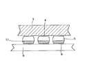
- FIG. 1is a schematic view of an example of BGA used in an embodiment of the invention.
- FIG. 2is a schematic view of the BGA to which a substrate is mounted.
- FIG. 3is a drawing showing a state in which the structure of the bumps is formed, after the completion of the mounting, of two phases, that is, the structure of the solder bumps 5 and the structure of a mixture layer 11 of both of the solder bumps and the solder for mounting.
- FIG. 4is a drawing showing another state in which the mixture layer 11 formed on the solder bumps 5 is thin in thickness with the result that fillets made of the solder for mounting are formed.
- FIG. 5is a drawing for explaining a method of distinguishing the mixture layer from the layer of the solder for mounting.
- FIG. 6is a table showing the results of evaluation obtained when BGAs each having bumps of Sn-3.5Ag-0.75Cu alloy solder are mounted by use of various solder pastes for mounting disclosed in the table.
- FIG. 7is a drawing showing a still another state in which the side portion of each of the bumps is surrounded by a part of the solder for mounting.
- FIG. 8is a drawing showing an example of multi-chip module (MCM).
- MCMmulti-chip module
- FIG. 9is a schematic view showing a state before mounting where the solder 22 of a wafer process package (WPP) is different from the mounting solder 28 of a BGA substrate.
- WPPwafer process package
- FIG. 10is a schematic view showing a state after mounting where the solder 22 of the WPP is different from the mounting solder 28 of the BGA substrate.
- FIG. 11is a schematic view showing a case of performing mounting on a substrate by use of solder 35 having a melting point lower than those of the bumps 22 of WPP and the bumps 27 of BGA.
- FIG. 12is a schematic view showing a state where the mounting of the substrate shown in FIG. 11 is finished.
- FIG. 13is a drawing showing WPP having a stress relaxation layer.
- FIG. 14is a drawing showing MCM in which WPP having the stress relaxation layer is mounted.
- FIG. 15is a drawing showing a case where a semiconductor device having a silicon substrate 70 is mounted on another substrate.
- FIG. 1a schematic view of an example of BGA used in the embodiment of the invention.
- the dimensions of a package used thereinis 30 mm ⁇ 30 mm, and a chip 2 located in the package has dimensions of 10 mm ⁇ 10 mm.
- Each of solder bumps 5has a diameter of 0.76 mm.
- Each of pads 4 formed on a BGA substrate 3has a diameter of 0.6 mm, which pads are made of copper metallized with the plating layer of Ni (of a thickness of 10 to 25 ⁇ m)/Au (of a thickness of 0.5 to 1.2 ⁇ m).
- the mounting substrate 9is FR-4 substrate having a thickness of 1 mm.
- Each of pads 8 provided on the substrate 9has a diameter of 0.6 mm, each of the pads 8 being formed of copper metallized with the layer of Ni (of a thickness of 2 ⁇ m)/Au (of a thickness of 0.03 ⁇ m).
- the mounting thereofis performed by the steps of: transferring on the pads 8 a solder paste 7 through a printing mask which solder paste contains solder particles and flux; performing the positioning of the bumps 5 and the pads 8 of the substrate 9 ; locating the BGA on the substrate 9 ; and performing the reflow heating thereof.
- Reflow heating at the time of the mountingmay be performed in an air atmosphere, however, in the embodiment of the invention the reflow heating was performed in a nitrogen atmosphere.
- the temperature of this reflow heatingwas the temperature of a soldering portion which temperature was actually measured by inserting a thermocouple 6 between one of the solder bumps 5 and one of the pads 7 located on the mounting substrate.
- the shape and composition of final bonding portionsvary in dependence on the combination of the materials of both of them, the volume ratio thereof, and the temperature of the reflow heating.
- the temperature of the reflow heatingis made to be not less than the melting point of the solder bumps 5 , each of the solder bumps 5 and the mounting solder 7 corresponding to each of the solder bumps 5 are completely dissolved each other, so that each of the bumps 10 comes to have a shape shown in FIG. 2 each of which bumps 10 has an even composition.
- the temperature of the reflow heatingmay be set so that the temperature between one of the solder bumps 5 and corresponding one of the pads 7 formed on the mounting substrate may become not less than the melting point of the solder bumps 5 , as in the case described above.
- the soldering portionshave the substantially same bonding structure as conventional bonding structure, and the reliability of bonding can be also obtained without any problem.
- the bump shape after the mounting(, that is, final bonding structure) varies in dependence on the temperature of the reflow heating.
- the bump shape after the mountingis the same as that of FIG. 2, the composition thereof is not even, that is, in each of the resultant bumps there are formed, as shown in FIG. 3, two layers of the original structure of the bumps 5 having been formed on the BGA substrate 3 and a mixture layer 11 of a mixture formed by the diffusion between the composition of the bumps 5 and the composition of the mounting solder 7 .
- the mixture layeris thin in thickness, and fillet is formed on the side of the mounting substrate which fillet is made of the solder 7 for mounting.
- the mixture layer 11 and the solder 7 for mounting both shown in FIG. 4it is possible to distinguish them from each other by the distribution of added elements contained in the solder 7 for mounting. For example, in a case where there exists a region 11 in which the rate of the added elements is low as shown in FIG. 5, this region 11 is judged to be the mixture layer of both of the bumps 5 and the solder 7 for mounting.
- this regionis judged to be the solder for mounting.
- the shape and structure of the bumps formed after the mountingvary in dependence on difference in melting point between the material of the solder bumps and the solder for mounting, the wettability thereof and the volume ratio thereof as well as the temperature of the reflow heating performed during the mounting.
- both of the mixture layer 11 and the solder 7 for mountingcome to be present, as shown in FIG. 7, even on the side portion of each of the bumps 5 for the BGA as well as in the vicinity of the substrate, so that there occurs such a shape as the solder 7 for mounting surrounds the periphery of each of the bumps 5 .
- the diameters of each of the bumps and each of the padsis 0.3 mm
- the diameter of each of openings in a printing mask for applying the solder for mountingbeing 0.3 mm
- the thickness thereofbeing 0.15 mm
- the volumes of each of the bumps 5 and the solder for mountingbecome 0.014 mm 3 and 0.0064 mm 3 , respectively
- the volume ratio of each of the bumps to the solder for mountingbecomes about 2:1
- a part of the solder for mountingcomes to be present on the side portion of each of the bumps 5 with the result that there occurs a shape similar to the bump structure shown in FIG. 7.
- this shapethere occurs no problem at all insofar as temperature cycling tests in the range of ⁇ 55 to 125° C. are concerned.
- the reliability thereofis improved because of increase in bonding area between each of the bumps 5 and the solder 7 for mounting.
- composition for the solder for mountingit is not limited to the Sn-1Ag-57Bi, but any solder composition having a melting point lower than that of the bumps may be used.
- bonding structureis obtained by the steps of using solder paste 7 for mounting which has a melting point lower than that of solder bumps 5 , and performing reflow heating at a temperature between the melting point of the solder bumps 5 and the melting point of the solder 7 for mounting.
- FIG. 6there are shown evaluation results obtained in temperature cycling tests performed, by using various solder pastes for mounting each having a melting point lower than that of solder bumps, in a temperature range of ⁇ 55 to 125° C. by 1000 cycles after performing the mounting while using Sn—Ag—Cu (Sn-3.5Ag-0.75Cu) alloy as the material of the solder bumps.
- this volume ratiovaries in dependence on the diameter of the bumps, the diameter of the pads, and the opening diameter and thickness of the printing mask, and the smaller the diameters of the bumps and the pads are (, that is, the smaller the pitch thereof becomes), the higher the ratio of the solder for mounting becomes.
- the melting point of the Sn-1Ag-57Bi solderis 137° C.
- the fillet portionscome to be softened. In the temperature cycles of 0 to 90° C., no occurrence of any crack was observed even after the 1000 cycles.
- the fillet portions of the above-described solder compositionBy forming the fillet portions of the above-described solder composition, the fillet portions are melted at a temperature not less than 137° C., whereby electronic parts having the above-described bump structure can be detached by heating the bump bonding portions by heating them up to a temperature not less than 137° C., so that the repair can be performed at a relatively low temperature.
- the temperature of the reflow heatingit is necessary to set the temperature of the reflow heating to be about 160° C. so that fillets of solder of low melting point may be formed.
- MCMmulti-chip module
- FIG. 8there are mounted on an intermediate substrate 25 a plurality of packages called WPP (Wafer Process Package) or wafer level CSP in each of which packages routing is provided on a silicon chip 20 and in each of which packages solder bumps 22 are formed on pads 21 provided on the chip 20 .
- the diameter of each of the bumps 27 formed on the intermediate substrate 25is 0.76 mm, the pitch thereof being 1.27 mm, the diameter of each of the bumps 21 of the WPP located above the intermediate substrate being 0.3 mm, and the pitch thereof is 0.5 mm.
- an underfill 24is formed at the bonding portions of the bumps after mounting the WPP.
- the bumps 22become external pads of the semiconductor device, the bumps 27 becoming external connection terminals, which is also applied to embodiments described below.
- FIG. 9is schematically shown the mounting of the WPP onto the intermediate substrate.
- solder paste 28was printed on the intermediate substrate 25 , both of the intermediate substrate 25 and the WPP being then positioned and being made to be abutted on each other, and the reflow heating thereof was performed to bond them to each other.
- the solder 22 used regarding the WPPwas made of a Sn-0.75Cu alloy
- the solder paste 28 printed on the intermediate substratewas made of a Sn-3Ag-0.5Cu alloy. Namely, these alloy compositions are selected so that the melting point of the solder 22 may become higher than that of the solder paste 28 .
- the bumps 27 provided on the intermediate substrate 25was made of the same Sn-3Ag-0.5Cu alloy as that of the solder paste 28 used for mounting the WPP.
- FIG. 10is a sectional view of this multi-chip module bonded to a mounting substrate, in which multi-chip module each of the bump portions of the WPP, which bump portions were formed at the side of the intermediate substrate 25 after the mounting of the WPP, does not have even composition but has a portion 30 of the original solder composition and a mixture layer 31 formed of the mixture of the Sn-0.75Cu (which is the composition of the WPP bumps) and the Sn-3Ag-0.5Cu (which is the composition of the solder for mounting).
- the solder of Sn—Ag—Cu alloythere is such a case as metallic acicular crystals called whiskers occur and reach adjacent bumps when the content of Ag contained in the solder is not less than 3 mass % with the result that short circuit fault is caused.
- the solder of the Sn—Cu alloy containing no Agwas used regarding the bumps formed on the WPP.
- the bumps 27is made of the Sn-3Ag-0.5Cu solder, however, the content of Ag contained in the mixture layer formed in each of the resultant bumps provided after the reflow heating becomes less than 3 mass %, so that there occurs no problem that the whiskers are caused.
- the composition of the solder used for the WPP bumpsno problem occurs even in a case where Sn-1Ag-0.5Cu containing 1 mass % Ag is used. In this case, the difference in melting point between the above Sn—Cu alloy and this Sn-1Ag-0.5Cu is only 1° C. Since, in the semiconductor devices mounted on the intermediate substrate 25 , there is used a narrower pitch design than that of the multi-chip module mounted on the mounting substrate 41 , the using of the solder, in which the content of Ag is reduced, at the time of performing the mounting on the intermediate substrate 25 is preferred in view of preventing the short circuit from occurring between the terminals due to the occurrence of the whiskers.
- the intermediate substrate 25has sufficiently high heat resisting property, it is possible to use a solder containing Ag of a low content regarding the bumps of the WPP and BGA and regarding the solder paste 28 while using regarding the mounting substrate another solder of so-called standard composition lower in melting point than that of the former solder.
- a solder containing Ag of a low content regarding the bumps of the WPP and BGA and regarding the solder paste 28while using regarding the mounting substrate another solder of so-called standard composition lower in melting point than that of the former solder.
- FIG. 11schematically shows a state just before mounting a multi-chip module with bumps 27 onto a substrate 41 by use of solder 35 (such as, for example, Sn-3Ag-0.5Cu solder) of a melting point lower than that of the bumps 27 while using Sn-0.75Cu alloy or Sn-1Ag-0.5Cu alloy regarding both of the bumps 22 of a semiconductor device and the bumps 27 of the multi-chip module
- solder 35such as, for example, Sn-3Ag-0.5Cu solder
- Sn-0.75Cu alloy or Sn-1Ag-0.5Cu alloyregarding both of the bumps 22 of a semiconductor device and the bumps 27 of the multi-chip module
- FIG. 12shows the sectional shape of a connection structure brought about after the mounting onto the substrate.
- the connection structure of the multi-chip module after the mountingthere are formed a portion 50 having the same composition as that of the original bumps and a mixture layer 51 made of a mixture of the compositions of the bumps and the solder for mounting.
- the multi-chip modulethere is such a case as temperature-hierarchical bonding is required between the solder bonding of a semiconductor device to be mounted on an intermediate substrate and the external connection terminals (,i.e., solder balls) of the multi-chip module. This is performed to keep the bonding of high reliability without causing, when soldering the multi-chip module to a circuit substrate, the re-melting of solder bonding already formed in the multi-chip module between the semiconductor device and the intermediate substrate.
- the above structure embodying the inventionit is possible to select, regarding the bumps 22 of the semiconductor device and the bumps 27 of the multi-chip module, such compositions as not to substantially melt at a reflow temperature at which the solder 35 for mounting is melted for bonding, whereby it becomes possible to realize the bonding of high reliability in the multi-chip module without performing the temperature-hierarchical bonding.
- the melting of the solder 35a part of each of the bumps 27 of the multi-chip module comes to be melted at the portion in contact with the melted solder 35 , so that the mixture layer 51 is formed.
- the solder used for the bumps 22 of the semiconductor devicemay be selected to have a composition higher in melting point than that of the solder material used for the bumps 27 of the multi-chip module. In any one of these cases, it is desired that the intermediate substrate has a heat resisting property higher than that of the mounting substrate.
- the WPPis a package having a silicon chip 20 provided with routing and bumps 22 each formed on each of chip-shaped pads 21 .
- the underfill 24is formed between the chip 20 and the intermediate substrate 25 to thereby reinforce the bumps.
- Means other than the underfillis to provide a stress relaxation layer 60 of a resin material between the chip and the bumps as shown in FIGS. 13 and 14. In this case, no underfill is required.
- FIG. 13corresponds to the structure of FIG. 10
- FIG. 14corresponds to the structure of FIG. 12.
- FIG. 15an example in which a semiconductor device using glass or silicon substrate 70 is mounted on a substrate 41 .
- a semiconductor device using glass or silicon substrate 70is mounted on the substrate 70 .
- wiring 72located around the substrate and stress relaxation layer 71 formed along the periphery thereof, and bumps 50 , 51 are formed on the stress relaxation layer 71 .
- a silicon chip 20 of WPPis mounted in the vicinity of the center of the lower side of the silicon substrate 70 through the bumps 22 toward a mounting substrate 41 .
- Solders 22 and 50 used at the lower side of the WPP and the stress relaxation layer 71are made of a composition containing no Ag or a small amount of Ag such as Sn-0.75Cu and Sn-1Ag-0.5Cu, and a solder for mounting on the substrate 41 is usually used Sn—Ag—Cu solder such as, for example, Sn-3Ag-0.5Cu.
- Sn—Ag—Cu soldersuch as, for example, Sn-3Ag-0.5Cu.
- a mixture layer 51is present which contain the composition of the solder for mounting.
- the silicon substrate 70there is no difference in physical properties between the silicon substrate 70 and the chip 20 . Thus, it is unnecessary to provide any underfill at the bonding portion formed by the bumps between the chip 20 of WPP and the silicon substrate 70 .
- the multi-chip module structureit becomes possible to prevent the whiskers from occurring by using, regarding the semiconductor device such as WPP or BGA, bumps made of Pb-free solder containing no or a small amount of Ag such as, for example, Sn-0 to about 2.0 mass % Ag— from about 0.3 to about 0.8 mass % Cu solder, and by using, when mounting this semiconductor device on the intermediate substrate, Sn— from about 2.5 to about 3.5 mass % Ag— from about 0.3 to about 0.8 mass % Cu solder which has a melting point lower than that of the former solder, and this structure makes it possible to perform the mounting of the multi-chip module having bumps arranged at a narrow pitch not more than 0.3 mm.
- the semiconductor devicesuch as WPP or BGA
- solder for mountingany one other than the Sn— from about 2.5 to about 3.5 mass % Ag— from about 0.3 to about 0.8 mass % Cu solder may be used, provided that the melting point of the solder bumps is higher than that of the solder for mounting.
- solder containing, for example, Bi or Sn—Zn soldermay be used.
Landscapes
- Engineering & Computer Science (AREA)
- Microelectronics & Electronic Packaging (AREA)
- Manufacturing & Machinery (AREA)
- Physics & Mathematics (AREA)
- Condensed Matter Physics & Semiconductors (AREA)
- General Physics & Mathematics (AREA)
- Computer Hardware Design (AREA)
- Power Engineering (AREA)
- Electric Connection Of Electric Components To Printed Circuits (AREA)
- Wire Bonding (AREA)
Abstract
Description
- The invention relates to technique for mounting a semiconductor device.[0001]
- There increases demand of semiconductor devices such as BGA, CSP, WPP, flip chip and etc. each of which semiconductor devices has bumps as external pads. In the semiconductor device having the bumps as the external pads, the bumps are formed by, for example, the steps of: preparing a pad pattern in which the plating of nickel-gold (Ni/Au) and nickel-palladium-gold (Ni/Pd/Au) is applied on the surface of copper; coating the pad pattern with flux by printing; mounting solder balls on the flux-coated pad pattern; and reflow-heating them so that the bumps may be formed.[0002]
- Further, the mounting of these semiconductor devices is performed by the steps of: coating a paste material, which comprises solder particles and flux, on a pad pattern formed on a substrate; positioning the bumps of the semiconductor device and the pad pattern of the substrate; locating the positioned bumps on the pad pattern; and them.[0003]
- Usually, a material used for the bumps or the mounting is so-called Sn—Pb eutectic solder of Sn-38 mass % Pb.[0004]
- In recent years, it is urged to put Pb-free solder to practical use.[0005]
- The melting point of the conventional Sn—Pb eutectic solder is 183° C. On the other hand, in a Pb-free solder material such as, for example, An—Ag—Cu solder, the melting point thereof ranges from 216° C. to 227° C., which melting point is higher than that of the conventional Sn—Pb eutectic solder.[0006]
- According to the research performed by the inventors of the invention, it is found that, in a case where a semiconductor device such as BGA which device has bumps is mounted on a substrate, there occurs such a phenomenon as the solder bumps do not always melt readily. Namely, according to the inventors' research, it is found that a temperature between the semiconductor device and the substrate is lower than the temperature of the substrate or the semiconductor device itself by a value of 15 to 20° C.[0007]
- Thus, by setting the reflow temperature so that these Pb-free solder bumps may be melted, the temperature of the substrate or the semiconductor device itself becomes higher by the value of 15 to 20° C. than the temperature measured between the semiconductor device and the substrate, that is, it becomes 240 to 260° C., so that there arises a problem of heat resisting property regarding the substrate and other electric parts (such as electrolytic capacitors and etc.) mounted on the substrate.[0008]
- The object of the invention is to realize solder bonding of high reliability in which the heat resisting properties of a circuit substrate and electronic parts are taken into consideration.[0009]
- In the invention, in order to achieve the object, there are provided the semiconductor module and the circuit substrate both recited in the claims.[0010]
- The inventors of the invention have noted the respects that, in a case of mounting on a substrate the semiconductor device such as BGA etc. which device has solder bumps, solder paste is fed on the substrate and that bonding portions are formed by the fed solder paste and the solder bumps. In prior arts, the solder paste and the solder bumps are formed of the same material, and they are usually melted completely so that the soldering may be achieved. However, in the invention, the solder bumps are not deemed to be a material for soldering but are deemed to be only pads, and the soldering of the pads (the solder bumps) is performed by the solder paste. Further, in the invention, the solder bumps are made of a material having a melting point higher than that of the solder paste so that each of the solder bumps may not be completely melted positively. As stated above, the temperatures of the bumps and the surrounding thereof are apt to become lower than the set reflow temperature, however, the solder paste is readily melted in comparison with the bumps, so that it is easy to perform the soldering.[0011]
- Thus, even at a reflow temperature at which each of the solder bumps is not melted completely, it becomes possible to realize, while taking the heat resistance of the circuit substrate and electric parts into consideration, soldering of high reliability in a case where bonding portions can be formed by the melting of the solder paste. For example, in a case where a semiconductor device having bumps as the outer pads thereof is mounted on a substrate by use of solder paste for mounting, the solder bumps are made of a material such as Sn—Cu alloy or Sn—Ag—Cu alloy which material has a melting point higher than that of conventional solder containing Pb, the solder for mounting the substrate being made to have a composition of a melting point lower than that of the solder bumps, and the reflow thereof is performed at such a temperature as the heat resisting properties of the substrate and the electric parts are taken into consideration, so that a mixture layer is formed between each of the solder bumps and the solder paste for mounting although each of the solder bumps is not melted completely with some of the original shape of each bump remaining, whereby it becomes possible to perform the bonding of both of the semiconductor device and the circuit substrate with high reliability. In this case, in order to prevent unexpected intermediate products from occurring during the forming of the mixture layer, it is preferred that the solder bumps have a solder composition of the same kind as that of the solder for mounting.[0012]
- Further, in a case of using the solder of the Sn—Ag—Cu alloy, there occur such problems as acicular crystals occur and as migration and short are caused due to the acicular crystals. Thus, it is desired to reduce the content of Ag contained in soldering portions formed between the semiconductor device and the circuit substrate. However, in the invention, the solder for mounting needs to have such a composition as to be melted at the reflow temperature, so that the composition of the solder is decided by the reflow temperature, that is, there is a limit regarding the reducing of the Ag content of the solder for mounting. Thus, it is preferred that, by reducing the amount of Ag inflowing from the solder bumps into the solder for mounting, the content of Ag contained in the soldering portions is prevented from increasing. Namely, it is preferred that the content of Ag contained in the solder bumps is less than that of the solder for mounting. For example, the solder balls (,i.e., solder bumps) may be made of Sn—Cu alloy solder. As regards the solder for mounting, the composition thereof is decided in accordance with the reflow temperature, and a Sn— about 2.0 to about 3.5 mass % Ag— about 0.3 to about 0.8 mass % Cu alloy is preferred in view of the reliability of bonding. In this specific case, it becomes preferred that the solder balls have the composition of Sn— zero to about 2.0 mass % Ag— about 0.3 to about 0.8 mass % Cu.[0013]
- FIG.[0014]1 is a schematic view of an example of BGA used in an embodiment of the invention.
- FIG. 2 is a schematic view of the BGA to which a substrate is mounted.[0015]
- FIG. 3 is a drawing showing a state in which the structure of the bumps is formed, after the completion of the mounting, of two phases, that is, the structure of the[0016]
solder bumps 5 and the structure of amixture layer 11 of both of the solder bumps and the solder for mounting. - FIG. 4 is a drawing showing another state in which the[0017]
mixture layer 11 formed on thesolder bumps 5 is thin in thickness with the result that fillets made of the solder for mounting are formed. - FIG. 5 is a drawing for explaining a method of distinguishing the mixture layer from the layer of the solder for mounting.[0018]
- FIG. 6 is a table showing the results of evaluation obtained when BGAs each having bumps of Sn-3.5Ag-0.75Cu alloy solder are mounted by use of various solder pastes for mounting disclosed in the table.[0019]
- FIG. 7 is a drawing showing a still another state in which the side portion of each of the bumps is surrounded by a part of the solder for mounting.[0020]
- FIG. 8 is a drawing showing an example of multi-chip module (MCM).[0021]
- FIG. 9 is a schematic view showing a state before mounting where the[0022]
solder 22 of a wafer process package (WPP) is different from themounting solder 28 of a BGA substrate. - FIG. 10 is a schematic view showing a state after mounting where the[0023]
solder 22 of the WPP is different from themounting solder 28 of the BGA substrate. - FIG. 11 is a schematic view showing a case of performing mounting on a substrate by use of[0024]
solder 35 having a melting point lower than those of thebumps 22 of WPP and thebumps 27 of BGA. - FIG. 12 is a schematic view showing a state where the mounting of the substrate shown in FIG. 11 is finished.[0025]
- FIG. 13 is a drawing showing WPP having a stress relaxation layer.[0026]
- FIG. 14 is a drawing showing MCM in which WPP having the stress relaxation layer is mounted.[0027]
- FIG. 15 is a drawing showing a case where a semiconductor device having a[0028]
silicon substrate 70 is mounted on another substrate. - The preferred embodiments of the invention are described below while referring to the drawings.[0029]
- FIG. 1 a schematic view of an example of BGA used in the embodiment of the invention. The dimensions of a package used therein is 30 mm×30 mm, and a[0030]
chip 2 located in the package has dimensions of 10 mm×10 mm. Each ofsolder bumps 5 has a diameter of 0.76 mm. Each ofpads 4 formed on aBGA substrate 3 has a diameter of 0.6 mm, which pads are made of copper metallized with the plating layer of Ni (of a thickness of 10 to 25 μm)/Au (of a thickness of 0.5 to 1.2 μm). Themounting substrate 9 is FR-4 substrate having a thickness of 1 mm. Each ofpads 8 provided on thesubstrate 9 has a diameter of 0.6 mm, each of thepads 8 being formed of copper metallized with the layer of Ni (of a thickness of 2 μm)/Au (of a thickness of 0.03 μm). The mounting thereof is performed by the steps of: transferring on the pads8 asolder paste 7 through a printing mask which solder paste contains solder particles and flux; performing the positioning of thebumps 5 and thepads 8 of thesubstrate 9; locating the BGA on thesubstrate 9; and performing the reflow heating thereof. - Reflow heating at the time of the mounting may be performed in an air atmosphere, however, in the embodiment of the invention the reflow heating was performed in a nitrogen atmosphere. The temperature of this reflow heating was the temperature of a soldering portion which temperature was actually measured by inserting a[0031]
thermocouple 6 between one of thesolder bumps 5 and one of thepads 7 located on the mounting substrate. - In such a case of the invention as the material of the[0032]
solder bumps 5 is made to be different from that of thesolder 7 for mounting (, that is, as the melting point of the solder for mounting is lower than that of the solder bumps5), the shape and composition of final bonding portions vary in dependence on the combination of the materials of both of them, the volume ratio thereof, and the temperature of the reflow heating. - First, in a case where the temperature of the reflow heating is made to be not less than the melting point of the[0033]
solder bumps 5, each of thesolder bumps 5 and themounting solder 7 corresponding to each of thesolder bumps 5 are completely dissolved each other, so that each of thebumps 10 comes to have a shape shown in FIG. 2 each of whichbumps 10 has an even composition. In a case where the substrate and other electronic parts have sufficient heat resisting properties, the temperature of the reflow heating may be set so that the temperature between one of thesolder bumps 5 and corresponding one of thepads 7 formed on the mounting substrate may become not less than the melting point of thesolder bumps 5, as in the case described above. In this case, the soldering portions have the substantially same bonding structure as conventional bonding structure, and the reliability of bonding can be also obtained without any problem. - Next, there is described below another case where the reflow heating is performed at a temperature between the melting point of the[0034]
solder bumps 5 and the melting point of thesolder 7 for mounting. In this case, the bump shape after the mounting (, that is, final bonding structure) varies in dependence on the temperature of the reflow heating. For example, as shown in FIG. 3, although the bump shape after the mounting is the same as that of FIG. 2, the composition thereof is not even, that is, in each of the resultant bumps there are formed, as shown in FIG. 3, two layers of the original structure of thebumps 5 having been formed on theBGA substrate 3 and amixture layer 11 of a mixture formed by the diffusion between the composition of thebumps 5 and the composition of themounting solder 7. Or, in each of the resultant bumps, as shown in FIG. 4, the mixture layer is thin in thickness, and fillet is formed on the side of the mounting substrate which fillet is made of thesolder 7 for mounting. As regards the distinction between themixture layer 11 and thesolder 7 for mounting both shown in FIG. 4, it is possible to distinguish them from each other by the distribution of added elements contained in thesolder 7 for mounting. For example, in a case where there exists aregion 11 in which the rate of the added elements is low as shown in FIG. 5, thisregion 11 is judged to be the mixture layer of both of thebumps 5 and thesolder 7 for mounting. On the other hand, in another case where there exists a region the composition of which is the substantially same as that of thesolder 7, this region is judged to be the solder for mounting. Further, it goes without saying that the shape and structure of the bumps formed after the mounting vary in dependence on difference in melting point between the material of the solder bumps and the solder for mounting, the wettability thereof and the volume ratio thereof as well as the temperature of the reflow heating performed during the mounting. - In a case where the ratio of the solder for mounting becomes high, both of the[0035]
mixture layer 11 and thesolder 7 for mounting come to be present, as shown in FIG. 7, even on the side portion of each of thebumps 5 for the BGA as well as in the vicinity of the substrate, so that there occurs such a shape as thesolder 7 for mounting surrounds the periphery of each of thebumps 5. For example, in a case where the diameters of each of the bumps and each of the pads is 0.3 mm, the diameter of each of openings in a printing mask for applying the solder for mounting being 0.3 mm, the thickness thereof being 0.15 mm, the volumes of each of thebumps 5 and the solder for mounting become 0.014 mm3and 0.0064 mm3, respectively, the volume ratio of each of the bumps to the solder for mounting becoming about 2:1, and a part of the solder for mounting comes to be present on the side portion of each of thebumps 5 with the result that there occurs a shape similar to the bump structure shown in FIG. 7. As regards this shape, there occurs no problem at all insofar as temperature cycling tests in the range of −55 to 125° C. are concerned. On the contrary, the reliability thereof is improved because of increase in bonding area between each of thebumps 5 and thesolder 7 for mounting. - Thus, in a case of the bonding structure shown in each of FIGS. 3, 4,[0036]5 and7 in which the melting point of the
solder paste 7 for mounting is lower than that of thebumps 5 and in which the reflow heating is performed to obtain this bonding structure at a temperature between the melting point of the solder bumps5 and the melting point of thesolder 7 for mounting, the solder bumps are not melted completely with some of each of the solder bumps remaining without melting, and it becomes possible, because of the occurrence of the mixture layer, to perform the bonding of high reliability between the semiconductor device and the circuit substrate. Accordingly, in comparison with the conventional method in which the solder bumps are completely melted, it becomes possible to perform the reflow while taking the heat resisting properties of the substrate and the electronic parts etc. into consideration. - Namely, in taking the bonding structure shown in FIG. 2 into consideration, it becomes possible to perform, by setting the reflow temperature to be a temperature at which at least the solder paste for mounting is melted, the bonding of high reliability between the semiconductor device and the substrate through any one of the bonding structures of FIGS. 2, 3,[0037]4,5 and7. In the prior arts, since the bonding is performed by completely melting the solder bumps and solder paste, there occur problems regarding the heat resisting properties of the substrate and electronic parts when the semiconductor device having the solder bumps is mounted. However, in the present invention, the solder bumps are not necessarily melted, so that the solving of the problems becomes easy.
- On the other hand, in a case of performing the bonding by mainly melting the solder for mounting, it become also possible to obtain repairable structure by using Sn-1Ag-57Bi solder (, in which the unit of each of the numerical values is mass percent, and this is also applied to all of the compositions described below,) of a low melting point (137° C.) as the solder for mounting. Namely, by feeding lead-free solder of a low melting point to a part of the circuit substrate onto which a semiconductor device such as BGA is to be mounted and by feeding usual lead-free solder of a high melting point to circuit substrate regions other than the former part, it becomes possible to detach an electronic part having the bump structure by heating the bump bonding portions of the semiconductor device up to a temperature not less than 137° C., whereby the repairing can be performed at a relatively low temperature. In a case where the repairing needs to be performed, it is preferred to set the temperature of the reflow heating to be about 160° C. to thereby form the fillet of solder having a low melting point. As regards the composition for the solder for mounting, it is not limited to the Sn-1Ag-57Bi, but any solder composition having a melting point lower than that of the bumps may be used. As a matter of course, the lower the melting point of the solder for mounting is, the lower the temperature of the repairing becomes, however, it goes without saying that the solder for mounting must have such a melting point as not to melt during usual operation.[0038]
- Next, the reliability of the bonding structure is described below which bonding structure is obtained by the steps of using[0039]
solder paste 7 for mounting which has a melting point lower than that ofsolder bumps 5, and performing reflow heating at a temperature between the melting point of the solder bumps5 and the melting point of thesolder 7 for mounting. - In FIG. 6 there are shown evaluation results obtained in temperature cycling tests performed, by using various solder pastes for mounting each having a melting point lower than that of solder bumps, in a temperature range of −55 to 125° C. by 1000 cycles after performing the mounting while using Sn—Ag—Cu (Sn-3.5Ag-0.75Cu) alloy as the material of the solder bumps.[0040]
- In the samples used in the experiments, when the diameter of each of the bumps (ball diameter of 0.76 mm) and the diameter of each of the pads were 0.60 mm, the volumes of each of the solder bumps and of the solder for mounting (, the diameter of each of openings in a printing mask being 0.76 mm, the thickness thereof being 0.1 mm, and the flux component of the solder for mounting being assumed to be 10%,) was 0.23 mm[0041]3and 0.04 mm3, respectively, and the volume ratio of each of the bumps and the solder for mounting was about 6:1. In general, this volume ratio varies in dependence on the diameter of the bumps, the diameter of the pads, and the opening diameter and thickness of the printing mask, and the smaller the diameters of the bumps and the pads are (, that is, the smaller the pitch thereof becomes), the higher the ratio of the solder for mounting becomes.
- In the cases where Sn-3Ag-5Bi and Sn-1Ag-57Bi were used as the[0042]
solder 7 for mounting, the bump structure shown in FIG. 3 was obtained. However, by making the temperature of the reflow heating more approach to the melting point of thesolder 7 for mounting, the shape of each of the bumps changes into one shown in FIG. 4. For example, in a case where the Sn-1Ag-57Bi used as thesolder 7 for mounting was heated at 165° C. during the reflow heating, a part of the solder was diffused into each of the solder bumps with the result that themixture layer 11 was formed, however, most of the solder for mounting came to form the fillet of the Sn-1Ag-57Bi on each of the pads formed on the mounting substrate. In another case where the temperature of the reflow heating was lowered down to 150° C. approaching the melting point of the Sn-1Ag-57Bi solder, such fillets as shown in FIG. 4 were formed although nodiffusion layer 11 was observed. Even in such a case as no diffusion phase is formed, there occurs no problem regarding the reliability of bonding, however, since the temperature of the reflow heating approaches the melting point of the solder for mounting, there occurs such a phenomenon as thesolder 7 for mounting does not melt regarding pads of relatively low temperature in a case where the variation of temperature in a package is large, and it is necessary to give care to this phenomenon. - The melting point of the Sn-1Ag-57Bi solder is 137° C. Thus, in a case of performing the temperature cycling tests in a temperature range of −55 to 125° C. regarding a mounted body having bump structure provided with the fillets, the fillet portions come to be softened. In the temperature cycles of 0 to 90° C., no occurrence of any crack was observed even after the 1000 cycles. By forming the fillet portions of the above-described solder composition, the fillet portions are melted at a temperature not less than 137° C., whereby electronic parts having the above-described bump structure can be detached by heating the bump bonding portions by heating them up to a temperature not less than 137° C., so that the repair can be performed at a relatively low temperature. Thus, when it is necessary to perform the repair, it is necessary to set the temperature of the reflow heating to be about 160° C. so that fillets of solder of low melting point may be formed.[0043]
- Accordingly, even in each of the cases where the reflow is performed at a temperature less than the melting point of the solder bumps, it becomes possible to keep the reliability of bonding.[0044]
- As described above, in the case where the semiconductor device having the Pb-free bumps of the high melting point is mounted to the substrate, it becomes possible to obtain the semiconductor device having the bump structure containing no Pb which semiconductor device also has the same level of reliability as that of conventional semiconductor devices.[0045]
- Next, there are described below examples in each of which this basic structure is applied to a multi-chip module (semiconductor module).[0046]
- In compliance with the requirements of the high integration design of a semiconductor, the small size design of the semiconductor device, and the mounting of high density, there is developed a multi-chip module (MCM) on which various semiconductors such as a memory, ASIC, and CPU are mounted or a multi-chip package in which these various semiconductors are packaged. One example thereof is shown in FIG. 8, in which the soldering structure described above is used in a multi-chip module.[0047]
- In FIG. 8, there are mounted on an intermediate substrate[0048]25 a plurality of packages called WPP (Wafer Process Package) or wafer level CSP in each of which packages routing is provided on a
silicon chip 20 and in each of which packages solder bumps22 are formed onpads 21 provided on thechip 20. The diameter of each of thebumps 27 formed on theintermediate substrate 25 is 0.76 mm, the pitch thereof being 1.27 mm, the diameter of each of thebumps 21 of the WPP located above the intermediate substrate being 0.3 mm, and the pitch thereof is 0.5 mm. In the WPP located above theintermediate substrate 25, anunderfill 24 is formed at the bonding portions of the bumps after mounting the WPP. In the multi-chip module, thebumps 22 become external pads of the semiconductor device, thebumps 27 becoming external connection terminals, which is also applied to embodiments described below. - In FIG. 9 is schematically shown the mounting of the WPP onto the intermediate substrate. In this case,[0049]
solder paste 28 was printed on theintermediate substrate 25, both of theintermediate substrate 25 and the WPP being then positioned and being made to be abutted on each other, and the reflow heating thereof was performed to bond them to each other. Thesolder 22 used regarding the WPP was made of a Sn-0.75Cu alloy, and thesolder paste 28 printed on the intermediate substrate was made of a Sn-3Ag-0.5Cu alloy. Namely, these alloy compositions are selected so that the melting point of thesolder 22 may become higher than that of thesolder paste 28. Thebumps 27 provided on theintermediate substrate 25 was made of the same Sn-3Ag-0.5Cu alloy as that of thesolder paste 28 used for mounting the WPP. - FIG. 10 is a sectional view of this multi-chip module bonded to a mounting substrate, in which multi-chip module each of the bump portions of the WPP, which bump portions were formed at the side of the[0050]
intermediate substrate 25 after the mounting of the WPP, does not have even composition but has aportion 30 of the original solder composition and amixture layer 31 formed of the mixture of the Sn-0.75Cu (which is the composition of the WPP bumps) and the Sn-3Ag-0.5Cu (which is the composition of the solder for mounting). - In general, in the solder of Sn—Ag—Cu alloy, there is such a case as metallic acicular crystals called whiskers occur and reach adjacent bumps when the content of Ag contained in the solder is not less than 3 mass % with the result that short circuit fault is caused. Thus, in the embodiment of the invention, in order to prevent the short circuit from occurring due to the whiskers, the solder of the Sn—Cu alloy containing no Ag was used regarding the bumps formed on the WPP. Incidentally, the[0051]
bumps 27 is made of the Sn-3Ag-0.5Cu solder, however, the content of Ag contained in the mixture layer formed in each of the resultant bumps provided after the reflow heating becomes less than 3 mass %, so that there occurs no problem that the whiskers are caused. As regards the composition of the solder used for the WPP bumps, no problem occurs even in a case where Sn-1Ag-0.5Cu containing 1 mass % Ag is used. In this case, the difference in melting point between the above Sn—Cu alloy and this Sn-1Ag-0.5Cu is only 1° C. Since, in the semiconductor devices mounted on theintermediate substrate 25, there is used a narrower pitch design than that of the multi-chip module mounted on the mountingsubstrate 41, the using of the solder, in which the content of Ag is reduced, at the time of performing the mounting on theintermediate substrate 25 is preferred in view of preventing the short circuit from occurring between the terminals due to the occurrence of the whiskers. - In a case where the[0052]
intermediate substrate 25 has sufficiently high heat resisting property, it is possible to use a solder containing Ag of a low content regarding the bumps of the WPP and BGA and regarding thesolder paste 28 while using regarding the mounting substrate another solder of so-called standard composition lower in melting point than that of the former solder. As a matter of course, it goes without saying that, in the mounting of the multi-chip module onto the mountingsubstrate 41, the above described structure of the invention can be applied. - Next, there is described below an example in which the above described soldering structure is used when mounting a multi-chip module onto a circuit substrate.[0053]
- FIG. 11 schematically shows a state just before mounting a multi-chip module with[0054]
bumps 27 onto asubstrate 41 by use of solder35 (such as, for example, Sn-3Ag-0.5Cu solder) of a melting point lower than that of thebumps 27 while using Sn-0.75Cu alloy or Sn-1Ag-0.5Cu alloy regarding both of thebumps 22 of a semiconductor device and thebumps 27 of the multi-chip module, and FIG. 12 shows the sectional shape of a connection structure brought about after the mounting onto the substrate. In the connection structure of the multi-chip module after the mounting, there are formed aportion 50 having the same composition as that of the original bumps and amixture layer 51 made of a mixture of the compositions of the bumps and the solder for mounting. - In the multi-chip module, there is such a case as temperature-hierarchical bonding is required between the solder bonding of a semiconductor device to be mounted on an intermediate substrate and the external connection terminals (,i.e., solder balls) of the multi-chip module. This is performed to keep the bonding of high reliability without causing, when soldering the multi-chip module to a circuit substrate, the re-melting of solder bonding already formed in the multi-chip module between the semiconductor device and the intermediate substrate.[0055]
- According to the above structure embodying the invention, it is possible to select, regarding the[0056]
bumps 22 of the semiconductor device and thebumps 27 of the multi-chip module, such compositions as not to substantially melt at a reflow temperature at which thesolder 35 for mounting is melted for bonding, whereby it becomes possible to realize the bonding of high reliability in the multi-chip module without performing the temperature-hierarchical bonding. In this case, by the melting of thesolder 35, a part of each of thebumps 27 of the multi-chip module comes to be melted at the portion in contact with the meltedsolder 35, so that themixture layer 51 is formed. As a matter of course, in a case where the re-melting occurring within the multi-chip module needs to be further restrained, the solder used for thebumps 22 of the semiconductor device may be selected to have a composition higher in melting point than that of the solder material used for thebumps 27 of the multi-chip module. In any one of these cases, it is desired that the intermediate substrate has a heat resisting property higher than that of the mounting substrate. - By the way, the WPP is a package having a[0057]
silicon chip 20 provided with routing and bumps22 each formed on each of chip-shapedpads 21. Thus, mounting on a printed board the WPP as it is causes such a fear as thebumps 22 are peeled off due to stress occurring because of the difference of physical properties (particularly thermal expansion) between thesilicon chip 20 and theintermediate substrate 25 which is the printed board. Thus, theunderfill 24 is formed between thechip 20 and theintermediate substrate 25 to thereby reinforce the bumps. Means other than the underfill is to provide astress relaxation layer 60 of a resin material between the chip and the bumps as shown in FIGS. 13 and 14. In this case, no underfill is required. Incidentally, FIG. 13 corresponds to the structure of FIG. 10, and FIG. 14 corresponds to the structure of FIG. 12. - Next, there is shown in FIG. 15 an example in which a semiconductor device using glass or[0058]
silicon substrate 70 is mounted on asubstrate 41. On thesubstrate 70 are providedwiring 72 located around the substrate andstress relaxation layer 71 formed along the periphery thereof, and bumps50,51 are formed on thestress relaxation layer 71. On the other hand, in the vicinity of the center of the lower side of thesilicon substrate 70 is mounted asilicon chip 20 of WPP through thebumps 22 toward a mountingsubstrate 41.Solders stress relaxation layer 71 are made of a composition containing no Ag or a small amount of Ag such as Sn-0.75Cu and Sn-1Ag-0.5Cu, and a solder for mounting on thesubstrate 41 is usually used Sn—Ag—Cu solder such as, for example, Sn-3Ag-0.5Cu. Thus, in the structure of the bumps formed after the mounting, amixture layer 51 is present which contain the composition of the solder for mounting. Regarding thesilicon substrate 70, there is no difference in physical properties between thesilicon substrate 70 and thechip 20. Thus, it is unnecessary to provide any underfill at the bonding portion formed by the bumps between thechip 20 of WPP and thesilicon substrate 70. - Thus, in the multi-chip module structure, it becomes possible to prevent the whiskers from occurring by using, regarding the semiconductor device such as WPP or BGA, bumps made of Pb-free solder containing no or a small amount of Ag such as, for example, Sn-0 to about 2.0 mass % Ag— from about 0.3 to about 0.8 mass % Cu solder, and by using, when mounting this semiconductor device on the intermediate substrate, Sn— from about 2.5 to about 3.5 mass % Ag— from about 0.3 to about 0.8 mass % Cu solder which has a melting point lower than that of the former solder, and this structure makes it possible to perform the mounting of the multi-chip module having bumps arranged at a narrow pitch not more than 0.3 mm. Of course, this is also applicable to the relation between the bumps provided in the multi-chip module and the solder for mounting which is provided on the mounting substrate. As regards the solder for mounting, any one other than the Sn— from about 2.5 to about 3.5 mass % Ag— from about 0.3 to about 0.8 mass % Cu solder may be used, provided that the melting point of the solder bumps is higher than that of the solder for mounting. In this case, solder containing, for example, Bi or Sn—Zn solder may be used.[0059]
- According to the invention, it becomes possible to realize the soldering of high reliability in which the heat resisting properties of the circuit substrate and the electronic parts are taken into consideration.[0060]
Claims (26)
Priority Applications (1)
| Application Number | Priority Date | Filing Date | Title |
|---|---|---|---|
| US10/265,660US7145236B2 (en) | 2000-06-12 | 2002-10-08 | Semiconductor device having solder bumps reliably reflow solderable |
Applications Claiming Priority (4)
| Application Number | Priority Date | Filing Date | Title |
|---|---|---|---|
| JP2000180712 | 2000-06-12 | ||
| JP2000-180712 | 2000-06-12 | ||
| US09/811,445US6486411B2 (en) | 2000-06-12 | 2001-03-20 | Semiconductor module having solder bumps and solder portions with different materials and compositions and circuit substrate |
| US10/265,660US7145236B2 (en) | 2000-06-12 | 2002-10-08 | Semiconductor device having solder bumps reliably reflow solderable |
Related Parent Applications (1)
| Application Number | Title | Priority Date | Filing Date |
|---|---|---|---|
| US09/811,445ContinuationUS6486411B2 (en) | 2000-06-12 | 2001-03-20 | Semiconductor module having solder bumps and solder portions with different materials and compositions and circuit substrate |
Publications (2)
| Publication Number | Publication Date |
|---|---|
| US20030030149A1true US20030030149A1 (en) | 2003-02-13 |
| US7145236B2 US7145236B2 (en) | 2006-12-05 |
Family
ID=18681745
Family Applications (2)
| Application Number | Title | Priority Date | Filing Date |
|---|---|---|---|
| US09/811,445Expired - LifetimeUS6486411B2 (en) | 2000-06-12 | 2001-03-20 | Semiconductor module having solder bumps and solder portions with different materials and compositions and circuit substrate |
| US10/265,660Expired - Fee RelatedUS7145236B2 (en) | 2000-06-12 | 2002-10-08 | Semiconductor device having solder bumps reliably reflow solderable |
Family Applications Before (1)
| Application Number | Title | Priority Date | Filing Date |
|---|---|---|---|
| US09/811,445Expired - LifetimeUS6486411B2 (en) | 2000-06-12 | 2001-03-20 | Semiconductor module having solder bumps and solder portions with different materials and compositions and circuit substrate |
Country Status (3)
| Country | Link |
|---|---|
| US (2) | US6486411B2 (en) |
| KR (1) | KR100398716B1 (en) |
| TW (1) | TWI230103B (en) |
Cited By (24)
| Publication number | Priority date | Publication date | Assignee | Title |
|---|---|---|---|---|
| US20020130163A1 (en)* | 2001-03-16 | 2002-09-19 | Seiko Epson Corporation | Soldering method, soldering device, and method and device of fabricating electronic circuit module |
| US6731003B2 (en)* | 2002-03-12 | 2004-05-04 | Fairchild Semiconductor Corporation | Wafer-level coated copper stud bumps |
| US20040219775A1 (en)* | 2002-12-26 | 2004-11-04 | Masashi Shimoyama | Lead free bump and method of forming the same |
| US6818987B2 (en)* | 2001-05-07 | 2004-11-16 | Ddk Ltd. | Electronic component and process for manufacturing the same |
| US20050258212A1 (en)* | 2004-05-14 | 2005-11-24 | Intevac, Inc. | Semiconductor die attachment for high vacuum tubes |
| US20050275098A1 (en)* | 2004-06-15 | 2005-12-15 | Advance Semiconductor Engineering Inc. | Lead-free conductive jointing bump |
| US20060113655A1 (en)* | 2004-05-14 | 2006-06-01 | Costello Kenneth A | Semiconductor die attachment for high vacuum tubes |
| US20060237231A1 (en)* | 2005-04-25 | 2006-10-26 | Shohei Hata | Substrate for mounting electronic part and electronic part |
| US20080128887A1 (en)* | 2004-12-13 | 2008-06-05 | Eiji Hayashi | Semiconductor Device |
| CN100424842C (en)* | 2004-11-17 | 2008-10-08 | 日本特殊陶业株式会社 | Manufacturing method of wiring board |
| US20090301760A1 (en)* | 2005-06-16 | 2009-12-10 | Masato Shimamura | Method of Soldering a Module Board |
| US7830021B1 (en)* | 2005-09-06 | 2010-11-09 | Rockwell Collins, Inc. | Tamper resistant packaging with transient liquid phase bonding |
| US20110006415A1 (en)* | 2009-07-13 | 2011-01-13 | Lsi Corporation | Solder interconnect by addition of copper |
| WO2011038090A1 (en)* | 2009-09-23 | 2011-03-31 | 3M Innovative Properties Company | Electrical connection and method for making the same |
| US20110272802A1 (en)* | 2008-05-12 | 2011-11-10 | Toshinori Ogashiwa | Bump, method for forming the bump, and method for mounting substrate having the bump thereon |
| US20120048914A1 (en)* | 2010-08-25 | 2012-03-01 | Ngk Spark Plug Co., Ltd. | Wiring substrate manufacturing method |
| KR20120058118A (en)* | 2010-11-29 | 2012-06-07 | 삼성전자주식회사 | Method of fabricating stacked package, and method of mounting stacked package fabricated by the same |
| CN103731983A (en)* | 2012-10-15 | 2014-04-16 | 三星电机株式会社 | Printed circuit board and method for manufacturing the same |
| CN104602862A (en)* | 2012-06-30 | 2015-05-06 | 千住金属工业株式会社 | Lead-free solder ball |
| WO2015147844A1 (en)* | 2014-03-27 | 2015-10-01 | Intel Corporation | Hybrid interconnect for low temperature attach |
| US20170066088A1 (en)* | 2015-09-04 | 2017-03-09 | Intel Corporation | Ball grid array (bga) apparatus and methods |
| US9620444B2 (en) | 2012-09-07 | 2017-04-11 | Mitsubishi Electric Corporation | Power semiconductor device |
| US20190067176A1 (en)* | 2016-03-22 | 2019-02-28 | Intel Corporation | Void reduction in solder joints using off-eutectic solder |
| US11830746B2 (en)* | 2021-01-05 | 2023-11-28 | Taiwan Semiconductor Manufacturing Co., Ltd. | Semiconductor device and method of manufacture |
Families Citing this family (57)
| Publication number | Priority date | Publication date | Assignee | Title |
|---|---|---|---|---|
| JP3444245B2 (en)* | 1999-09-03 | 2003-09-08 | 日本電気株式会社 | Soldering method to electroless nickel / gold plating, wiring structure, circuit device and manufacturing method thereof |
| KR100407448B1 (en)* | 2000-06-12 | 2003-11-28 | 가부시키가이샤 히타치세이사쿠쇼 | Electronic apparatus and semiconductor device |
| KR100398716B1 (en)* | 2000-06-12 | 2003-09-19 | 가부시키가이샤 히타치세이사쿠쇼 | Semiconductor module and circuit substrate |
| US6696765B2 (en)* | 2001-11-19 | 2004-02-24 | Hitachi, Ltd. | Multi-chip module |
| US6889429B2 (en)* | 2001-03-26 | 2005-05-10 | Semiconductor Components Industries, L.L.C. | Method of making a lead-free integrated circuit package |
| KR100400606B1 (en)* | 2001-09-08 | 2003-10-08 | 정재필 | Double pre-coated substrate using lead free solder plated with low-melting-pointed alloy and manufacturing method thereof |
| JP2003234433A (en)* | 2001-10-01 | 2003-08-22 | Matsushita Electric Ind Co Ltd | Semiconductor device, method of mounting semiconductor device, and package and method of manufacturing the same |
| JP2003198116A (en)* | 2001-12-28 | 2003-07-11 | Matsushita Electric Ind Co Ltd | Soldering method and joint structure |
| JP3897596B2 (en)* | 2002-01-07 | 2007-03-28 | 日本テキサス・インスツルメンツ株式会社 | Mounted body of semiconductor device and wiring board |
| US6933505B2 (en)* | 2002-03-13 | 2005-08-23 | Oy Ajat Ltd | Low temperature, bump-bonded radiation imaging device |
| TWI284973B (en)* | 2002-04-03 | 2007-08-01 | Advanced Semiconductor Eng | Flip-chip joint structure, and fabricating process thereof |
| US20040155358A1 (en)* | 2003-02-07 | 2004-08-12 | Toshitsune Iijima | First and second level packaging assemblies and method of assembling package |
| KR100698662B1 (en)* | 2003-12-02 | 2007-03-23 | 에프씨엠 가부시끼가이샤 | Terminals forming surfaces consisting of tin-silver-copper ternary alloys, parts and articles |
| JP3997991B2 (en)* | 2004-01-14 | 2007-10-24 | セイコーエプソン株式会社 | Electronic equipment |
| JP2005211946A (en)* | 2004-01-30 | 2005-08-11 | Renesas Technology Corp | Solder alloy and semiconductor device |
| US7287685B2 (en)* | 2004-09-20 | 2007-10-30 | International Business Machines Corporation | Structure and method to gain substantial reliability improvements in lead-free BGAs assembled with lead-bearing solders |
| JP4524454B2 (en)* | 2004-11-19 | 2010-08-18 | ルネサスエレクトロニクス株式会社 | Electronic device and manufacturing method thereof |
| US7394150B2 (en)* | 2004-11-23 | 2008-07-01 | Siliconix Incorporated | Semiconductor package including die interposed between cup-shaped lead frame and lead frame having mesas and valleys |
| US7238551B2 (en)* | 2004-11-23 | 2007-07-03 | Siliconix Incorporated | Method of fabricating semiconductor package including die interposed between cup-shaped lead frame having mesas and valleys |
| KR100690245B1 (en)* | 2005-04-06 | 2007-03-12 | 삼성전자주식회사 | Solder Bonding Method Using Low Melting Point Solder and Repair Method of Ball Grid Array Package Using the Same |
| US7838997B2 (en) | 2005-06-14 | 2010-11-23 | John Trezza | Remote chip attachment |
| US7781886B2 (en) | 2005-06-14 | 2010-08-24 | John Trezza | Electronic chip contact structure |
| US8456015B2 (en) | 2005-06-14 | 2013-06-04 | Cufer Asset Ltd. L.L.C. | Triaxial through-chip connection |
| US7786592B2 (en) | 2005-06-14 | 2010-08-31 | John Trezza | Chip capacitive coupling |
| US7851348B2 (en) | 2005-06-14 | 2010-12-14 | Abhay Misra | Routingless chip architecture |
| US7767493B2 (en) | 2005-06-14 | 2010-08-03 | John Trezza | Post & penetration interconnection |
| US7687400B2 (en) | 2005-06-14 | 2010-03-30 | John Trezza | Side stacking apparatus and method |
| US7989958B2 (en) | 2005-06-14 | 2011-08-02 | Cufer Assett Ltd. L.L.C. | Patterned contact |
| US7560813B2 (en) | 2005-06-14 | 2009-07-14 | John Trezza | Chip-based thermo-stack |
| US20070037004A1 (en)* | 2005-08-12 | 2007-02-15 | Antaya Technologies Corporation | Multilayer solder article |
| US20070231594A1 (en)* | 2005-08-12 | 2007-10-04 | John Pereira | Multilayer solder article |
| US20080175748A1 (en)* | 2005-08-12 | 2008-07-24 | John Pereira | Solder Composition |
| US20070036670A1 (en)* | 2005-08-12 | 2007-02-15 | John Pereira | Solder composition |
| US20070292708A1 (en)* | 2005-08-12 | 2007-12-20 | John Pereira | Solder composition |
| JP4742844B2 (en)* | 2005-12-15 | 2011-08-10 | ルネサスエレクトロニクス株式会社 | Manufacturing method of semiconductor device |
| US7626274B2 (en)* | 2006-02-03 | 2009-12-01 | Texas Instruments Incorporated | Semiconductor device with an improved solder joint |
| US7687397B2 (en) | 2006-06-06 | 2010-03-30 | John Trezza | Front-end processed wafer having through-chip connections |
| JP5266235B2 (en) | 2006-10-17 | 2013-08-21 | フライズ・メタルズ・インコーポレイテッド | Method for providing an electrical connection in an electrical device |
| US7670874B2 (en) | 2007-02-16 | 2010-03-02 | John Trezza | Plated pillar package formation |
| KR101067429B1 (en) | 2008-04-03 | 2011-09-27 | 르네사스 일렉트로닉스 가부시키가이샤 | Method for manufacturing semiconductor device and semiconductor device manufactured by this method |
| KR100969441B1 (en) | 2008-06-05 | 2010-07-14 | 삼성전기주식회사 | Printed circuit board mounted with semiconductor chip and manufacturing method |
| JP5316261B2 (en)* | 2009-06-30 | 2013-10-16 | 富士通株式会社 | Multichip module, printed circuit board unit and electronic device |
| JP2011044571A (en)* | 2009-08-20 | 2011-03-03 | Renesas Electronics Corp | Semiconductor device, external connection terminal, method of manufacturing semiconductor device, and method of manufacturing external connection terminal |
| US9064881B2 (en)* | 2010-11-11 | 2015-06-23 | Taiwan Semiconductor Manufacturing Company, Ltd. | Protecting flip-chip package using pre-applied fillet |
| EP2679334B1 (en)* | 2011-02-25 | 2020-05-27 | Senju Metal Industry Co., Ltd | Use of a solder alloy and soldered joint of high current density |
| KR101811301B1 (en)* | 2011-05-24 | 2017-12-26 | 삼성전자주식회사 | Semiconductor package |
| JP2013000359A (en)* | 2011-06-16 | 2013-01-07 | Toshiba Corp | Endoscope apparatus and electronic apparatus |
| IN2014DN07833A (en)* | 2012-03-20 | 2015-04-24 | Alpha Metals | |
| US20140151096A1 (en)* | 2012-12-04 | 2014-06-05 | Hongjin Jiang | Low temperature/high temperature solder hybrid solder interconnects |
| US9748157B1 (en)* | 2013-05-29 | 2017-08-29 | STATS ChipPAC Pte. Ltd. | Integrated circuit packaging system with joint assembly and method of manufacture thereof |
| JP6307131B2 (en)* | 2015-09-08 | 2018-04-04 | エルジー エレクトロニクス インコーポレイティド | Solar cell module and manufacturing method thereof |
| CN105499738B (en)* | 2016-01-21 | 2017-12-29 | 深圳市科美达自动化设备有限公司 | The tin-soldering method of carbon brush motor rotor commutator pin |
| WO2018063415A1 (en)* | 2016-10-01 | 2018-04-05 | Intel Corporation | Indium solder metallurgy to control electro-migration |
| JP2021093417A (en)* | 2019-12-09 | 2021-06-17 | イビデン株式会社 | Print circuit board and manufacturing method of print circuit board |
| DE102022101056A1 (en) | 2022-01-18 | 2023-07-20 | STANNOL GmbH & Co. KG | Process for achieving a reliable brazed joint and master alloys therefor |
| CN115430949B (en)* | 2022-10-09 | 2024-04-05 | 云南锡业集团(控股)有限责任公司研发中心 | Five-membered eutectic high-toughness low-Wen Xibi-series solder and preparation method thereof |
| CN117976637B (en)* | 2024-04-01 | 2024-07-05 | 甬矽半导体(宁波)有限公司 | Bump package structure and method for manufacturing bump package structure |
Citations (16)
| Publication number | Priority date | Publication date | Assignee | Title |
|---|---|---|---|---|
| US4825284A (en)* | 1985-12-11 | 1989-04-25 | Hitachi, Ltd. | Semiconductor resin package structure |
| US4970577A (en)* | 1988-04-12 | 1990-11-13 | Hitachi, Ltd. | Semiconductor chip module |
| US5405577A (en)* | 1993-04-29 | 1995-04-11 | Seelig; Karl F. | Lead-free and bismuth-free tin alloy solder composition |
| US5849606A (en)* | 1995-08-25 | 1998-12-15 | Hitachi, Ltd. | Semiconductor device and manufacturing of the same |
| US5874043A (en)* | 1996-06-12 | 1999-02-23 | International Business Machines Corporation | Lead-free, high tin ternary solder alloy of tin, silver, and indium |
| US5942185A (en)* | 1994-10-11 | 1999-08-24 | Hitachi, Ltd. | Lead-free solder used for connecting electronic parts on organic substrate and electronic products made using same |
| US5985212A (en)* | 1996-12-12 | 1999-11-16 | H-Technologies Group, Incorporated | High strength lead-free solder materials |
| US5998861A (en)* | 1995-09-28 | 1999-12-07 | Kabushiki Kaisha Toshiba | Semiconductor device having ball grid array |
| US6104093A (en)* | 1997-04-24 | 2000-08-15 | International Business Machines Corporation | Thermally enhanced and mechanically balanced flip chip package and method of forming |
| US6160308A (en)* | 1999-03-10 | 2000-12-12 | Kabushiki Kaisha Toshiba | Semiconductor device |
| US6224690B1 (en)* | 1995-12-22 | 2001-05-01 | International Business Machines Corporation | Flip-Chip interconnections using lead-free solders |
| US6228680B1 (en)* | 1998-05-06 | 2001-05-08 | Texas Instruments Incorporated | Low stress method and apparatus for underfilling flip-chip electronic devices |
| US6257215B1 (en)* | 1999-03-18 | 2001-07-10 | Hitachi, Ltd. | Resin-sealed electronic apparatus for use in internal combustion engines |
| US6337445B1 (en)* | 1998-03-16 | 2002-01-08 | Texas Instruments Incorporated | Composite connection structure and method of manufacturing |
| US20020089836A1 (en)* | 1999-10-26 | 2002-07-11 | Kenzo Ishida | Injection molded underfill package and method of assembly |
| US6486411B2 (en)* | 2000-06-12 | 2002-11-26 | Hitachi, Ltd. | Semiconductor module having solder bumps and solder portions with different materials and compositions and circuit substrate |
Family Cites Families (5)
| Publication number | Priority date | Publication date | Assignee | Title |
|---|---|---|---|---|
| JPS63289947A (en)* | 1987-05-22 | 1988-11-28 | Toshiba Corp | Substrate with solder bumps and manufacturing method thereof |
| WO1997009455A1 (en)* | 1995-09-01 | 1997-03-13 | Sarnoff Corporation | Soldering composition |
| JP3736819B2 (en)* | 1997-01-17 | 2006-01-18 | 株式会社豊田中央研究所 | Lead-free solder alloy |
| JPH10314980A (en)* | 1997-05-14 | 1998-12-02 | Sony Corp | Solder material |
| JP2000101014A (en) | 1998-09-22 | 2000-04-07 | Hitachi Ltd | Semiconductor device |
- 2001
- 2001-03-19KRKR10-2001-0014030Apatent/KR100398716B1/ennot_activeExpired - Fee Related
- 2001-03-20USUS09/811,445patent/US6486411B2/ennot_activeExpired - Lifetime
- 2001-03-26TWTW090107100Apatent/TWI230103B/ennot_activeIP Right Cessation
- 2002
- 2002-10-08USUS10/265,660patent/US7145236B2/ennot_activeExpired - Fee Related
Patent Citations (16)
| Publication number | Priority date | Publication date | Assignee | Title |
|---|---|---|---|---|
| US4825284A (en)* | 1985-12-11 | 1989-04-25 | Hitachi, Ltd. | Semiconductor resin package structure |
| US4970577A (en)* | 1988-04-12 | 1990-11-13 | Hitachi, Ltd. | Semiconductor chip module |
| US5405577A (en)* | 1993-04-29 | 1995-04-11 | Seelig; Karl F. | Lead-free and bismuth-free tin alloy solder composition |
| US5942185A (en)* | 1994-10-11 | 1999-08-24 | Hitachi, Ltd. | Lead-free solder used for connecting electronic parts on organic substrate and electronic products made using same |
| US5849606A (en)* | 1995-08-25 | 1998-12-15 | Hitachi, Ltd. | Semiconductor device and manufacturing of the same |
| US5998861A (en)* | 1995-09-28 | 1999-12-07 | Kabushiki Kaisha Toshiba | Semiconductor device having ball grid array |
| US6224690B1 (en)* | 1995-12-22 | 2001-05-01 | International Business Machines Corporation | Flip-Chip interconnections using lead-free solders |
| US5874043A (en)* | 1996-06-12 | 1999-02-23 | International Business Machines Corporation | Lead-free, high tin ternary solder alloy of tin, silver, and indium |
| US5985212A (en)* | 1996-12-12 | 1999-11-16 | H-Technologies Group, Incorporated | High strength lead-free solder materials |
| US6104093A (en)* | 1997-04-24 | 2000-08-15 | International Business Machines Corporation | Thermally enhanced and mechanically balanced flip chip package and method of forming |
| US6337445B1 (en)* | 1998-03-16 | 2002-01-08 | Texas Instruments Incorporated | Composite connection structure and method of manufacturing |
| US6228680B1 (en)* | 1998-05-06 | 2001-05-08 | Texas Instruments Incorporated | Low stress method and apparatus for underfilling flip-chip electronic devices |
| US6160308A (en)* | 1999-03-10 | 2000-12-12 | Kabushiki Kaisha Toshiba | Semiconductor device |
| US6257215B1 (en)* | 1999-03-18 | 2001-07-10 | Hitachi, Ltd. | Resin-sealed electronic apparatus for use in internal combustion engines |
| US20020089836A1 (en)* | 1999-10-26 | 2002-07-11 | Kenzo Ishida | Injection molded underfill package and method of assembly |
| US6486411B2 (en)* | 2000-06-12 | 2002-11-26 | Hitachi, Ltd. | Semiconductor module having solder bumps and solder portions with different materials and compositions and circuit substrate |
Cited By (48)
| Publication number | Priority date | Publication date | Assignee | Title |
|---|---|---|---|---|
| US6732907B2 (en)* | 2001-03-16 | 2004-05-11 | Seiko Epson Corporation | Soldering method, soldering device, and method and device of fabricating electronic circuit module |
| US20020130163A1 (en)* | 2001-03-16 | 2002-09-19 | Seiko Epson Corporation | Soldering method, soldering device, and method and device of fabricating electronic circuit module |
| US6818987B2 (en)* | 2001-05-07 | 2004-11-16 | Ddk Ltd. | Electronic component and process for manufacturing the same |
| US6731003B2 (en)* | 2002-03-12 | 2004-05-04 | Fairchild Semiconductor Corporation | Wafer-level coated copper stud bumps |
| US20040219775A1 (en)* | 2002-12-26 | 2004-11-04 | Masashi Shimoyama | Lead free bump and method of forming the same |
| US7012333B2 (en)* | 2002-12-26 | 2006-03-14 | Ebara Corporation | Lead free bump and method of forming the same |
| US7608533B2 (en)* | 2004-05-14 | 2009-10-27 | Intevac, Inc. | Semiconductor die attachment for high vacuum tubes |
| US20050258212A1 (en)* | 2004-05-14 | 2005-11-24 | Intevac, Inc. | Semiconductor die attachment for high vacuum tubes |
| US20060113655A1 (en)* | 2004-05-14 | 2006-06-01 | Costello Kenneth A | Semiconductor die attachment for high vacuum tubes |
| US7607560B2 (en) | 2004-05-14 | 2009-10-27 | Intevac, Inc. | Semiconductor die attachment for high vacuum tubes |
| US20050275098A1 (en)* | 2004-06-15 | 2005-12-15 | Advance Semiconductor Engineering Inc. | Lead-free conductive jointing bump |
| CN100424842C (en)* | 2004-11-17 | 2008-10-08 | 日本特殊陶业株式会社 | Manufacturing method of wiring board |
| US20080128887A1 (en)* | 2004-12-13 | 2008-06-05 | Eiji Hayashi | Semiconductor Device |
| US20110163444A1 (en)* | 2004-12-13 | 2011-07-07 | Renesas Electronics Corporation | Semiconductor device having elastic solder bump to prevent disconnection |
| US8101514B2 (en) | 2004-12-13 | 2012-01-24 | Renesas Electronics Corporation | Semiconductor device having elastic solder bump to prevent disconnection |
| US20100255673A1 (en)* | 2004-12-13 | 2010-10-07 | Renesas Technology Corp. | Semiconductor device having elastic solder bump to prevent disconnection |
| US7951701B2 (en)* | 2004-12-13 | 2011-05-31 | Renesas Electronics Corporation | Semiconductor device having elastic solder bump to prevent disconnection |
| US7759793B2 (en)* | 2004-12-13 | 2010-07-20 | Renesas Technology Corp. | Semiconductor device having elastic solder bump to prevent disconnection |
| US7511232B2 (en)* | 2005-04-25 | 2009-03-31 | Hitachi Kyowa Engineering Co., Ltd. | Substrate for mounting electronic part and electronic part |
| US20060237231A1 (en)* | 2005-04-25 | 2006-10-26 | Shohei Hata | Substrate for mounting electronic part and electronic part |
| US7842889B2 (en) | 2005-04-25 | 2010-11-30 | Hitachi Kyowa Engineering Co., Ltd. | Substrate for mounting electronic part and electronic part |
| US20090126991A1 (en)* | 2005-04-25 | 2009-05-21 | Shohei Hata | Substrate for mounting electronic part and electronic part |
| US20090301760A1 (en)* | 2005-06-16 | 2009-12-10 | Masato Shimamura | Method of Soldering a Module Board |
| US7830021B1 (en)* | 2005-09-06 | 2010-11-09 | Rockwell Collins, Inc. | Tamper resistant packaging with transient liquid phase bonding |
| US8492894B2 (en)* | 2008-05-12 | 2013-07-23 | Tanaka Kikinzoku Kogyo K.K. | Bump, method for forming the bump, and method for mounting substrate having the bump thereon |
| US20110272802A1 (en)* | 2008-05-12 | 2011-11-10 | Toshinori Ogashiwa | Bump, method for forming the bump, and method for mounting substrate having the bump thereon |
| US8962471B2 (en) | 2009-03-06 | 2015-02-24 | Tanaka Kikinzoku Kogyo K.K. | Bump, method for forming the bump, and method for mounting substrate having the bump thereon |
| US20110006415A1 (en)* | 2009-07-13 | 2011-01-13 | Lsi Corporation | Solder interconnect by addition of copper |
| US8378485B2 (en)* | 2009-07-13 | 2013-02-19 | Lsi Corporation | Solder interconnect by addition of copper |
| WO2011038090A1 (en)* | 2009-09-23 | 2011-03-31 | 3M Innovative Properties Company | Electrical connection and method for making the same |
| US20120048914A1 (en)* | 2010-08-25 | 2012-03-01 | Ngk Spark Plug Co., Ltd. | Wiring substrate manufacturing method |
| US8322596B2 (en)* | 2010-08-25 | 2012-12-04 | Ngk Spark Plug Co., Ltd. | Wiring substrate manufacturing method |
| US20120252163A1 (en)* | 2010-11-29 | 2012-10-04 | Jae-Wook Yoo | Stacked package, method of fabricating stacked package, and method of mounting stacked package fabricated by the method |
| KR101712459B1 (en)* | 2010-11-29 | 2017-03-22 | 삼성전자 주식회사 | Method of fabricating stacked package, and method of mounting stacked package fabricated by the same |
| US8735221B2 (en)* | 2010-11-29 | 2014-05-27 | Samsung Electronics Co., Ltd. | Stacked package, method of fabricating stacked package, and method of mounting stacked package fabricated by the method |
| US20140232005A1 (en)* | 2010-11-29 | 2014-08-21 | Samsung Electronics Co., Ltd. | Stacked package, method of fabricating stacked package, and method of mounting stacked package fabricated by the method |
| KR20120058118A (en)* | 2010-11-29 | 2012-06-07 | 삼성전자주식회사 | Method of fabricating stacked package, and method of mounting stacked package fabricated by the same |
| CN104602862A (en)* | 2012-06-30 | 2015-05-06 | 千住金属工业株式会社 | Lead-free solder ball |
| US9620444B2 (en) | 2012-09-07 | 2017-04-11 | Mitsubishi Electric Corporation | Power semiconductor device |
| CN103731983A (en)* | 2012-10-15 | 2014-04-16 | 三星电机株式会社 | Printed circuit board and method for manufacturing the same |
| GB2540060A (en)* | 2014-03-27 | 2017-01-04 | Intel Corp | Hybrid interconnect for low temperature attach |
| WO2015147844A1 (en)* | 2014-03-27 | 2015-10-01 | Intel Corporation | Hybrid interconnect for low temperature attach |
| GB2540060B (en)* | 2014-03-27 | 2019-02-13 | Intel Corp | Hybrid interconnect for low temperature attach |
| DE112014006271B4 (en) | 2014-03-27 | 2023-03-09 | Intel Corporation | Hybrid interconnect for low temperature attachment and method of making same |
| US20170066088A1 (en)* | 2015-09-04 | 2017-03-09 | Intel Corporation | Ball grid array (bga) apparatus and methods |
| US20190067176A1 (en)* | 2016-03-22 | 2019-02-28 | Intel Corporation | Void reduction in solder joints using off-eutectic solder |
| US11830746B2 (en)* | 2021-01-05 | 2023-11-28 | Taiwan Semiconductor Manufacturing Co., Ltd. | Semiconductor device and method of manufacture |
| US12417927B2 (en) | 2021-01-05 | 2025-09-16 | Taiwan Semiconductor Manufacturing Co., Ltd. | Semiconductor device and method of manufacture |
Also Published As
| Publication number | Publication date |
|---|---|
| KR20010112057A (en) | 2001-12-20 |
| KR100398716B1 (en) | 2003-09-19 |
| US20010050181A1 (en) | 2001-12-13 |
| TWI230103B (en) | 2005-04-01 |
| US7145236B2 (en) | 2006-12-05 |
| US6486411B2 (en) | 2002-11-26 |
Similar Documents
| Publication | Publication Date | Title |
|---|---|---|
| US6486411B2 (en) | Semiconductor module having solder bumps and solder portions with different materials and compositions and circuit substrate | |
| US5730932A (en) | Lead-free, tin-based multi-component solder alloys | |
| US6657124B2 (en) | Advanced electronic package | |
| US6010060A (en) | Lead-free solder process | |
| US6176947B1 (en) | Lead-free solders | |
| US6574859B2 (en) | Interconnection process for module assembly and rework | |
| KR100790978B1 (en) | Bonding method at low temperature, and semiconductor package mounting method using same | |
| EP0769346A1 (en) | Composite solder paste for flip chip bumping | |
| KR101279291B1 (en) | Lead-free solder joint structure and solder ball | |
| US20060043603A1 (en) | Low temperature PB-free processing for semiconductor devices | |
| JP4211828B2 (en) | Mounting structure | |
| US20060097398A1 (en) | Method and structure to reduce risk of gold embrittlement in solder joints | |
| US6619536B2 (en) | Solder process and solder alloy therefor | |
| JP4366838B2 (en) | Method for manufacturing electronic circuit module | |
| KR100648039B1 (en) | Solder Ball Forming Method and Manufacturing Method and Structure of Semiconductor Package Using the Same | |
| JP4940662B2 (en) | Solder bump, method of forming solder bump, and semiconductor device | |
| JP2002076605A (en) | Circuit board connecting semiconductor module and semiconductor device | |
| JP4027534B2 (en) | Electronic component mounting method | |
| JPH0888297A (en) | Electronic component and electronic component connection structure | |
| JP2000151086A (en) | Printed circuit unit and method of manufacturing the same | |
| JP3594442B2 (en) | Semiconductor device | |
| JP3469093B2 (en) | Manufacturing method of printed circuit board and mounted circuit board | |
| JPH0864717A (en) | Mounting method of circuit parts | |
| CN117712035A (en) | Composite welding spot low-temperature interconnection method for solving substrate warpage problem | |
| JPH04297090A (en) | Mounting method for electronic component |
Legal Events
| Date | Code | Title | Description |
|---|---|---|---|
| AS | Assignment | Owner name:RENESAS TECHNOLOGY CORPORATION, JAPAN Free format text:ASSIGNMENT OF ASSIGNORS INTEREST;ASSIGNOR:HITACHI, LTD.;REEL/FRAME:014569/0585 Effective date:20030912 | |
| FEPP | Fee payment procedure | Free format text:PAYOR NUMBER ASSIGNED (ORIGINAL EVENT CODE: ASPN); ENTITY STATUS OF PATENT OWNER: LARGE ENTITY | |
| FPAY | Fee payment | Year of fee payment:4 | |
| AS | Assignment | Owner name:RENESAS ELECTRONICS CORPORATION, JAPAN Free format text:MERGER/CHANGE OF NAME;ASSIGNOR:RENESAS TECHNOLOGY CORP.;REEL/FRAME:026837/0505 Effective date:20100401 | |
| FPAY | Fee payment | Year of fee payment:8 | |
| AS | Assignment | Owner name:RENESAS ELECTRONICS CORPORATION, JAPAN Free format text:CHANGE OF ADDRESS;ASSIGNOR:RENESAS ELECTRONICS CORPORATION;REEL/FRAME:044928/0001 Effective date:20150806 | |
| FEPP | Fee payment procedure | Free format text:MAINTENANCE FEE REMINDER MAILED (ORIGINAL EVENT CODE: REM.) | |
| LAPS | Lapse for failure to pay maintenance fees | Free format text:PATENT EXPIRED FOR FAILURE TO PAY MAINTENANCE FEES (ORIGINAL EVENT CODE: EXP.); ENTITY STATUS OF PATENT OWNER: LARGE ENTITY | |
| STCH | Information on status: patent discontinuation | Free format text:PATENT EXPIRED DUE TO NONPAYMENT OF MAINTENANCE FEES UNDER 37 CFR 1.362 | |
| FP | Lapsed due to failure to pay maintenance fee | Effective date:20181205 |