US20030030131A1 - Semiconductor package apparatus and method - Google Patents
Semiconductor package apparatus and methodDownload PDFInfo
- Publication number
- US20030030131A1 US20030030131A1US10/262,848US26284802AUS2003030131A1US 20030030131 A1US20030030131 A1US 20030030131A1US 26284802 AUS26284802 AUS 26284802AUS 2003030131 A1US2003030131 A1US 2003030131A1
- Authority
- US
- United States
- Prior art keywords
- pad
- lead frame
- encapsulation
- semiconductor package
- leads
- Prior art date
- Legal status (The legal status is an assumption and is not a legal conclusion. Google has not performed a legal analysis and makes no representation as to the accuracy of the status listed.)
- Abandoned
Links
- 239000004065semiconductorSubstances0.000titleclaimsabstractdescription116
- 238000000034methodMethods0.000titleclaimsdescription42
- 238000005538encapsulationMethods0.000claimsabstractdescription42
- 238000000465mouldingMethods0.000claimsdescription62
- 238000004519manufacturing processMethods0.000claimsdescription19
- 239000011159matrix materialSubstances0.000claimsdescription18
- 239000011347resinSubstances0.000claimsdescription17
- 229920005989resinPolymers0.000claimsdescription17
- 238000005530etchingMethods0.000claimsdescription8
- 238000003825pressingMethods0.000claimsdescription4
- 238000005520cutting processMethods0.000claimsdescription2
- KDLHZDBZIXYQEI-UHFFFAOYSA-NPalladiumChemical compound[Pd]KDLHZDBZIXYQEI-UHFFFAOYSA-N0.000description8
- PXHVJJICTQNCMI-UHFFFAOYSA-NNickelChemical compound[Ni]PXHVJJICTQNCMI-UHFFFAOYSA-N0.000description4
- 238000005516engineering processMethods0.000description4
- 229910052763palladiumInorganic materials0.000description4
- 239000004642PolyimideSubstances0.000description3
- 238000007747platingMethods0.000description3
- 229920001721polyimidePolymers0.000description3
- 229910052709silverInorganic materials0.000description3
- 239000004332silverSubstances0.000description3
- 239000000853adhesiveSubstances0.000description2
- 230000001070adhesive effectEffects0.000description2
- 239000000463materialSubstances0.000description2
- 229910052759nickelInorganic materials0.000description2
- 238000000926separation methodMethods0.000description2
- 238000009966trimmingMethods0.000description2
- BQCADISMDOOEFD-UHFFFAOYSA-NSilverChemical compound[Ag]BQCADISMDOOEFD-UHFFFAOYSA-N0.000description1
- 239000004809TeflonSubstances0.000description1
- 229920006362Teflon®Polymers0.000description1
- 239000012790adhesive layerSubstances0.000description1
- 230000002411adverseEffects0.000description1
- 238000001311chemical methods and processMethods0.000description1
- 230000007423decreaseEffects0.000description1
- 230000000694effectsEffects0.000description1
- 239000010410layerSubstances0.000description1
- 229910000510noble metalInorganic materials0.000description1
- 230000002265preventionEffects0.000description1
- 238000004080punchingMethods0.000description1
- 238000003466weldingMethods0.000description1
Images


Classifications
- H—ELECTRICITY
- H01—ELECTRIC ELEMENTS
- H01L—SEMICONDUCTOR DEVICES NOT COVERED BY CLASS H10
- H01L21/00—Processes or apparatus adapted for the manufacture or treatment of semiconductor or solid state devices or of parts thereof
- H01L21/02—Manufacture or treatment of semiconductor devices or of parts thereof
- H01L21/04—Manufacture or treatment of semiconductor devices or of parts thereof the devices having potential barriers, e.g. a PN junction, depletion layer or carrier concentration layer
- H01L21/50—Assembly of semiconductor devices using processes or apparatus not provided for in a single one of the groups H01L21/18 - H01L21/326 or H10D48/04 - H10D48/07 e.g. sealing of a cap to a base of a container
- H01L21/56—Encapsulations, e.g. encapsulation layers, coatings
- H01L21/565—Moulds
- H—ELECTRICITY
- H01—ELECTRIC ELEMENTS
- H01L—SEMICONDUCTOR DEVICES NOT COVERED BY CLASS H10
- H01L23/00—Details of semiconductor or other solid state devices
- H01L23/28—Encapsulations, e.g. encapsulating layers, coatings, e.g. for protection
- H01L23/31—Encapsulations, e.g. encapsulating layers, coatings, e.g. for protection characterised by the arrangement or shape
- H01L23/3107—Encapsulations, e.g. encapsulating layers, coatings, e.g. for protection characterised by the arrangement or shape the device being completely enclosed
- H—ELECTRICITY
- H01—ELECTRIC ELEMENTS
- H01L—SEMICONDUCTOR DEVICES NOT COVERED BY CLASS H10
- H01L23/00—Details of semiconductor or other solid state devices
- H01L23/48—Arrangements for conducting electric current to or from the solid state body in operation, e.g. leads, terminal arrangements ; Selection of materials therefor
- H01L23/488—Arrangements for conducting electric current to or from the solid state body in operation, e.g. leads, terminal arrangements ; Selection of materials therefor consisting of soldered or bonded constructions
- H01L23/495—Lead-frames or other flat leads
- H01L23/49541—Geometry of the lead-frame
- H01L23/49548—Cross section geometry
- H01L23/49551—Cross section geometry characterised by bent parts
- H—ELECTRICITY
- H01—ELECTRIC ELEMENTS
- H01L—SEMICONDUCTOR DEVICES NOT COVERED BY CLASS H10
- H01L2224/00—Indexing scheme for arrangements for connecting or disconnecting semiconductor or solid-state bodies and methods related thereto as covered by H01L24/00
- H01L2224/01—Means for bonding being attached to, or being formed on, the surface to be connected, e.g. chip-to-package, die-attach, "first-level" interconnects; Manufacturing methods related thereto
- H01L2224/42—Wire connectors; Manufacturing methods related thereto
- H01L2224/44—Structure, shape, material or disposition of the wire connectors prior to the connecting process
- H01L2224/45—Structure, shape, material or disposition of the wire connectors prior to the connecting process of an individual wire connector
- H01L2224/45001—Core members of the connector
- H01L2224/45099—Material
- H—ELECTRICITY
- H01—ELECTRIC ELEMENTS
- H01L—SEMICONDUCTOR DEVICES NOT COVERED BY CLASS H10
- H01L2224/00—Indexing scheme for arrangements for connecting or disconnecting semiconductor or solid-state bodies and methods related thereto as covered by H01L24/00
- H01L2224/01—Means for bonding being attached to, or being formed on, the surface to be connected, e.g. chip-to-package, die-attach, "first-level" interconnects; Manufacturing methods related thereto
- H01L2224/42—Wire connectors; Manufacturing methods related thereto
- H01L2224/47—Structure, shape, material or disposition of the wire connectors after the connecting process
- H01L2224/48—Structure, shape, material or disposition of the wire connectors after the connecting process of an individual wire connector
- H01L2224/4805—Shape
- H01L2224/4809—Loop shape
- H01L2224/48091—Arched
- H—ELECTRICITY
- H01—ELECTRIC ELEMENTS
- H01L—SEMICONDUCTOR DEVICES NOT COVERED BY CLASS H10
- H01L2224/00—Indexing scheme for arrangements for connecting or disconnecting semiconductor or solid-state bodies and methods related thereto as covered by H01L24/00
- H01L2224/01—Means for bonding being attached to, or being formed on, the surface to be connected, e.g. chip-to-package, die-attach, "first-level" interconnects; Manufacturing methods related thereto
- H01L2224/42—Wire connectors; Manufacturing methods related thereto
- H01L2224/47—Structure, shape, material or disposition of the wire connectors after the connecting process
- H01L2224/48—Structure, shape, material or disposition of the wire connectors after the connecting process of an individual wire connector
- H01L2224/481—Disposition
- H01L2224/48151—Connecting between a semiconductor or solid-state body and an item not being a semiconductor or solid-state body, e.g. chip-to-substrate, chip-to-passive
- H01L2224/48221—Connecting between a semiconductor or solid-state body and an item not being a semiconductor or solid-state body, e.g. chip-to-substrate, chip-to-passive the body and the item being stacked
- H01L2224/48245—Connecting between a semiconductor or solid-state body and an item not being a semiconductor or solid-state body, e.g. chip-to-substrate, chip-to-passive the body and the item being stacked the item being metallic
- H01L2224/48247—Connecting between a semiconductor or solid-state body and an item not being a semiconductor or solid-state body, e.g. chip-to-substrate, chip-to-passive the body and the item being stacked the item being metallic connecting the wire to a bond pad of the item
- H—ELECTRICITY
- H01—ELECTRIC ELEMENTS
- H01L—SEMICONDUCTOR DEVICES NOT COVERED BY CLASS H10
- H01L2224/00—Indexing scheme for arrangements for connecting or disconnecting semiconductor or solid-state bodies and methods related thereto as covered by H01L24/00
- H01L2224/01—Means for bonding being attached to, or being formed on, the surface to be connected, e.g. chip-to-package, die-attach, "first-level" interconnects; Manufacturing methods related thereto
- H01L2224/42—Wire connectors; Manufacturing methods related thereto
- H01L2224/47—Structure, shape, material or disposition of the wire connectors after the connecting process
- H01L2224/48—Structure, shape, material or disposition of the wire connectors after the connecting process of an individual wire connector
- H01L2224/481—Disposition
- H01L2224/48151—Connecting between a semiconductor or solid-state body and an item not being a semiconductor or solid-state body, e.g. chip-to-substrate, chip-to-passive
- H01L2224/48221—Connecting between a semiconductor or solid-state body and an item not being a semiconductor or solid-state body, e.g. chip-to-substrate, chip-to-passive the body and the item being stacked
- H01L2224/48245—Connecting between a semiconductor or solid-state body and an item not being a semiconductor or solid-state body, e.g. chip-to-substrate, chip-to-passive the body and the item being stacked the item being metallic
- H01L2224/48257—Connecting between a semiconductor or solid-state body and an item not being a semiconductor or solid-state body, e.g. chip-to-substrate, chip-to-passive the body and the item being stacked the item being metallic connecting the wire to a die pad of the item
- H—ELECTRICITY
- H01—ELECTRIC ELEMENTS
- H01L—SEMICONDUCTOR DEVICES NOT COVERED BY CLASS H10
- H01L2224/00—Indexing scheme for arrangements for connecting or disconnecting semiconductor or solid-state bodies and methods related thereto as covered by H01L24/00
- H01L2224/01—Means for bonding being attached to, or being formed on, the surface to be connected, e.g. chip-to-package, die-attach, "first-level" interconnects; Manufacturing methods related thereto
- H01L2224/42—Wire connectors; Manufacturing methods related thereto
- H01L2224/47—Structure, shape, material or disposition of the wire connectors after the connecting process
- H01L2224/49—Structure, shape, material or disposition of the wire connectors after the connecting process of a plurality of wire connectors
- H01L2224/491—Disposition
- H01L2224/49105—Connecting at different heights
- H01L2224/49109—Connecting at different heights outside the semiconductor or solid-state body
- H—ELECTRICITY
- H01—ELECTRIC ELEMENTS
- H01L—SEMICONDUCTOR DEVICES NOT COVERED BY CLASS H10
- H01L2224/00—Indexing scheme for arrangements for connecting or disconnecting semiconductor or solid-state bodies and methods related thereto as covered by H01L24/00
- H01L2224/80—Methods for connecting semiconductor or other solid state bodies using means for bonding being attached to, or being formed on, the surface to be connected
- H01L2224/85—Methods for connecting semiconductor or other solid state bodies using means for bonding being attached to, or being formed on, the surface to be connected using a wire connector
- H01L2224/8538—Bonding interfaces outside the semiconductor or solid-state body
- H01L2224/85399—Material
- H01L2224/854—Material with a principal constituent of the material being a metal or a metalloid, e.g. boron (B), silicon (Si), germanium (Ge), arsenic (As), antimony (Sb), tellurium (Te) and polonium (Po), and alloys thereof
- H01L2224/85438—Material with a principal constituent of the material being a metal or a metalloid, e.g. boron (B), silicon (Si), germanium (Ge), arsenic (As), antimony (Sb), tellurium (Te) and polonium (Po), and alloys thereof the principal constituent melting at a temperature of greater than or equal to 950°C and less than 1550°C
- H01L2224/85439—Silver (Ag) as principal constituent
- H—ELECTRICITY
- H01—ELECTRIC ELEMENTS
- H01L—SEMICONDUCTOR DEVICES NOT COVERED BY CLASS H10
- H01L2224/00—Indexing scheme for arrangements for connecting or disconnecting semiconductor or solid-state bodies and methods related thereto as covered by H01L24/00
- H01L2224/80—Methods for connecting semiconductor or other solid state bodies using means for bonding being attached to, or being formed on, the surface to be connected
- H01L2224/85—Methods for connecting semiconductor or other solid state bodies using means for bonding being attached to, or being formed on, the surface to be connected using a wire connector
- H01L2224/8538—Bonding interfaces outside the semiconductor or solid-state body
- H01L2224/85399—Material
- H01L2224/854—Material with a principal constituent of the material being a metal or a metalloid, e.g. boron (B), silicon (Si), germanium (Ge), arsenic (As), antimony (Sb), tellurium (Te) and polonium (Po), and alloys thereof
- H01L2224/85438—Material with a principal constituent of the material being a metal or a metalloid, e.g. boron (B), silicon (Si), germanium (Ge), arsenic (As), antimony (Sb), tellurium (Te) and polonium (Po), and alloys thereof the principal constituent melting at a temperature of greater than or equal to 950°C and less than 1550°C
- H01L2224/85455—Nickel (Ni) as principal constituent
- H—ELECTRICITY
- H01—ELECTRIC ELEMENTS
- H01L—SEMICONDUCTOR DEVICES NOT COVERED BY CLASS H10
- H01L2224/00—Indexing scheme for arrangements for connecting or disconnecting semiconductor or solid-state bodies and methods related thereto as covered by H01L24/00
- H01L2224/80—Methods for connecting semiconductor or other solid state bodies using means for bonding being attached to, or being formed on, the surface to be connected
- H01L2224/85—Methods for connecting semiconductor or other solid state bodies using means for bonding being attached to, or being formed on, the surface to be connected using a wire connector
- H01L2224/8538—Bonding interfaces outside the semiconductor or solid-state body
- H01L2224/85399—Material
- H01L2224/854—Material with a principal constituent of the material being a metal or a metalloid, e.g. boron (B), silicon (Si), germanium (Ge), arsenic (As), antimony (Sb), tellurium (Te) and polonium (Po), and alloys thereof
- H01L2224/85463—Material with a principal constituent of the material being a metal or a metalloid, e.g. boron (B), silicon (Si), germanium (Ge), arsenic (As), antimony (Sb), tellurium (Te) and polonium (Po), and alloys thereof the principal constituent melting at a temperature of greater than 1550°C
- H01L2224/85464—Palladium (Pd) as principal constituent
- H—ELECTRICITY
- H01—ELECTRIC ELEMENTS
- H01L—SEMICONDUCTOR DEVICES NOT COVERED BY CLASS H10
- H01L24/00—Arrangements for connecting or disconnecting semiconductor or solid-state bodies; Methods or apparatus related thereto
- H01L24/01—Means for bonding being attached to, or being formed on, the surface to be connected, e.g. chip-to-package, die-attach, "first-level" interconnects; Manufacturing methods related thereto
- H01L24/42—Wire connectors; Manufacturing methods related thereto
- H01L24/47—Structure, shape, material or disposition of the wire connectors after the connecting process
- H01L24/48—Structure, shape, material or disposition of the wire connectors after the connecting process of an individual wire connector
- H—ELECTRICITY
- H01—ELECTRIC ELEMENTS
- H01L—SEMICONDUCTOR DEVICES NOT COVERED BY CLASS H10
- H01L24/00—Arrangements for connecting or disconnecting semiconductor or solid-state bodies; Methods or apparatus related thereto
- H01L24/01—Means for bonding being attached to, or being formed on, the surface to be connected, e.g. chip-to-package, die-attach, "first-level" interconnects; Manufacturing methods related thereto
- H01L24/42—Wire connectors; Manufacturing methods related thereto
- H01L24/47—Structure, shape, material or disposition of the wire connectors after the connecting process
- H01L24/49—Structure, shape, material or disposition of the wire connectors after the connecting process of a plurality of wire connectors
- H—ELECTRICITY
- H01—ELECTRIC ELEMENTS
- H01L—SEMICONDUCTOR DEVICES NOT COVERED BY CLASS H10
- H01L2924/00—Indexing scheme for arrangements or methods for connecting or disconnecting semiconductor or solid-state bodies as covered by H01L24/00
- H01L2924/0001—Technical content checked by a classifier
- H01L2924/00014—Technical content checked by a classifier the subject-matter covered by the group, the symbol of which is combined with the symbol of this group, being disclosed without further technical details
- H—ELECTRICITY
- H01—ELECTRIC ELEMENTS
- H01L—SEMICONDUCTOR DEVICES NOT COVERED BY CLASS H10
- H01L2924/00—Indexing scheme for arrangements or methods for connecting or disconnecting semiconductor or solid-state bodies as covered by H01L24/00
- H01L2924/01—Chemical elements
- H01L2924/01046—Palladium [Pd]
- H—ELECTRICITY
- H01—ELECTRIC ELEMENTS
- H01L—SEMICONDUCTOR DEVICES NOT COVERED BY CLASS H10
- H01L2924/00—Indexing scheme for arrangements or methods for connecting or disconnecting semiconductor or solid-state bodies as covered by H01L24/00
- H01L2924/01—Chemical elements
- H01L2924/01078—Platinum [Pt]
- H—ELECTRICITY
- H01—ELECTRIC ELEMENTS
- H01L—SEMICONDUCTOR DEVICES NOT COVERED BY CLASS H10
- H01L2924/00—Indexing scheme for arrangements or methods for connecting or disconnecting semiconductor or solid-state bodies as covered by H01L24/00
- H01L2924/15—Details of package parts other than the semiconductor or other solid state devices to be connected
- H01L2924/151—Die mounting substrate
- H01L2924/153—Connection portion
- H01L2924/1532—Connection portion the connection portion being formed on the die mounting surface of the substrate
- H—ELECTRICITY
- H01—ELECTRIC ELEMENTS
- H01L—SEMICONDUCTOR DEVICES NOT COVERED BY CLASS H10
- H01L2924/00—Indexing scheme for arrangements or methods for connecting or disconnecting semiconductor or solid-state bodies as covered by H01L24/00
- H01L2924/15—Details of package parts other than the semiconductor or other solid state devices to be connected
- H01L2924/161—Cap
- H01L2924/1615—Shape
- H01L2924/16152—Cap comprising a cavity for hosting the device, e.g. U-shaped cap
- H—ELECTRICITY
- H01—ELECTRIC ELEMENTS
- H01L—SEMICONDUCTOR DEVICES NOT COVERED BY CLASS H10
- H01L2924/00—Indexing scheme for arrangements or methods for connecting or disconnecting semiconductor or solid-state bodies as covered by H01L24/00
- H01L2924/15—Details of package parts other than the semiconductor or other solid state devices to be connected
- H01L2924/181—Encapsulation
- H01L2924/183—Connection portion, e.g. seal
- H01L2924/18301—Connection portion, e.g. seal being an anchoring portion, i.e. mechanical interlocking between the encapsulation resin and another package part
Definitions
- the present inventionrelates to a lead frame, a semiconductor package having the lead frame, and a method for manufacturing the semiconductor package, and more particularly, to a lead frame in which a flash phenomenon occurring to molding resin in a semiconductor package can be prevented, a semiconductor package having the lead frame, and a method for manufacturing the semiconductor package.
- a semiconductor packageis formed by arranging a semiconductor chip on a pad of a lead frame, wire-bonding an electrode of the semiconductor chip and an inner lead of the lead frame, and encapsulating the pad and the inner lead frame with molding resin.
- a chip scale package(CSP) is developed. While leads protrude from the side surface of a semiconductor package in the conventional semiconductor package, in the chip scale package, leads protrude from the bottom surface of the semiconductor package. If the leads protrude from the bottom surface of the semiconductor package, the size of the package drastically decreases and a space occupied by the package is further reduced. To expose leads to the bottom surface of the package, the leads need to be down-set or half-etched. The exposed leads contact terminals on a printed circuit board. In some particular cases, a pad on which a semiconductor chip is arranged is exposed to the bottom surface of the package.
- CSPchip scale package
- FIG. 1is a sectional view of a semiconductor package according to a conventional technology, which is disclosed in Japanese Patent Publication No. 59-21047.
- a semiconductor chip 14is mounted on the upper surface of a pad 11 and a lead 12 is down-set processed.
- a bottom surface 12 a of the lead 12is exposed to the bottom surface of an encapsulation 15 so that the lead 12 can contact a connection terminal (not shown) on a printed circuit board.
- An upper end of the lead 12 and an electrode (not shown) of the semiconductor chip 14are connected by a bonding wire 13 .
- the pad 11is positioned lower than the upper end of the lead 12 .
- the semiconductor package of FIG. 1is a typical example in which the lead 12 is down-set processed.
- FIG. 2shows another example of a semiconductor package according to the conventional technology, which is disclosed in Japanese Patent Publication No. 59-227143.
- a semiconductor chip 24is mounted on a pad 21 .
- a lead 22is processed by a half-etching method so that a bottom surface 22 a thereof is exposed to the bottom surface of an encapsulation 25 .
- One end of the lead 22 and an electrode of the semiconductor chip 24are connected by a bonding wire 23 .
- the semiconductor package of FIG. 2is an example in which lead 22 is half-etched.
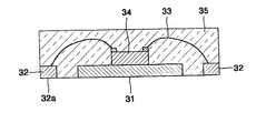
- FIG. 3shows yet another example of a semiconductor package according to a conventional technology, which is disclosed in U.S. Pat. No. 6,143,981.
- a semiconductor chip 34is mounted on an upper surface of a pad 31 .
- a bottom surface of the pad 31 and a bottom surface 32 a of a lead 32are exposed from the bottom surface of an encapsulation 35 . That is, the pad 31 and the lead 32 are formed at the same height.
- the lead 32 and electrodes of the semiconductor chip 34are connected by a bonding wire 33 .
- the exposed lead 32contacts a connection terminal on a printed circuit board.
- the bottom surface of the exposed pad 31radiates heat generated by the semiconductor chip 34 to the outside.
- the exposed pad 31is connected to a thermal pad (not shown) on the printed circuit board.
- the semiconductor package of FIG. 3is an example in which the pad 31 is exposed to the outside.
- a semiconductor package described with reference to FIG. 3When a semiconductor package described with reference to FIG. 3 is to be manufactured, there are typically two conventional manufacturing methods that can be applied.
- the first methodthere is a lead frame unit including a separate lead frame 41 and a rail 42 encompassing the lead frame 41 from the outside, as shown in FIG. 4.
- the lead frame unitundergoes wafer sawing, die attach, wire bonding, molding/deflashing, marking, and trimming/forming.
- the merit of using a lead frame to which trimming is applied individuallyis that generation of flash to mold is relatively restricted. However, complete prevention of the flash generation is not possible so that an additional step of removing the flash is actually needed.
- a lead frameis not individually trimmed, but a lead frame unit in which a plurality of lead frames are arranged in form of matrix is molded together.
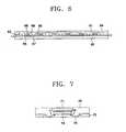
- the lead frame unit in form of matrixis shown in FIG. 5.
- reference numeral 51denotes an individual lead frame
- reference numeral 52denotes a rail encompassing each lead frame from the outside.
- the matrix type lead frame unitis assembled by steps of wafer sawing, die attach, wire bonding, molding/deflashing, marking, and singulation by sawing.
- the individually trimmed lead framehas smaller unit density per unit area because the unit area on a lead frame strip is greater than the unit area of the matrix type.
- a unit price per unit areaincreases.
- the matrix type lead frameis more frequently used.
- mold flashcan be generated in a molding step such that application of a matrix type lead frame is not possible.
- FIG. 6shows a molding step of a semiconductor package which corresponds to a molding step using a matrix type lead frame.
- molding of a semiconductor packageis formed in a molding plate including an upper plate 61 and a lower plate 62 .
- the spacewill be filled with molding resin 64 .
- the molding resin 64may be injected into the space through a gate 63 .
- the lead frameis provided with a pad 65 and a lead 67 and a semiconductor chip 66 is mounted on the upper surface of the pad 65 .
- An electrode of the semiconductor chip 66 and the lead 67are connected by a bonding wire 68 .
- the lead frameis of a matrix type shown in FIG. 5, which has not cut yet into individual lead frames.
- a method using a rear side tapeis introduced. That is, a heat-resistant tape such as polyimide or Teflon is laminated on the rear side of the lead frame. Since an adhesive layer is present on the polyimide tape, the polyimide tape is attached to the inner surface of the lower plate so that generation of flash can be prevented.
- the method using the rear side tapeuses a special tape of a particular company, cost is high and an additional step is needed, increasing an investment cost. Also, after the tape is removed, the adhesive remains on the surface of the lead frame so that a degree of welding is lowered. To remove the adhesive, a chemical process is required.
- a lead frame for an encapsulated semiconductor package having a predetermined thicknesscomprising a pad for receiving a semiconductor chip, the pad having a top surface, a support portion having a bottom surface and a plurality of leads formed on the support portion, a resilient tie bar having a first end connected to the pad and a second end connected to the support portion, the tie bar when in an unstressed condition supporting the pad such that the top surface of the pad and the bottom surface of the supporting portion and leads are separated by a distance greater than the predetermined thickness.
- tie baris down-set processed.
- At least a portion of the plurality of leadsis half-etched.
- the half-etched portionis electrically connected to the semiconductor chip.
- the lead frame when in a stressed conditionis configured to fit into a space defined by a pair of molding plates separated by a distance of the predetermined thickness.
- an encapsulated semiconductor packagehaving a predetermined thickness, comprising a pad having a first surface and a second surface opposite to the first surface, a support portion having a bottom surface and a plurality of leads formed on the support portion, a semiconductor chip attached to the first surface of the pad, a resilient tie bar having a first end connected to the pad and a second end connected to the support portion, and an encapsulation having a first surface and a second surface opposite to the first surface, the second surface of the pad being exposed to the first surface of the encapsulation and the leads being exposed to the second surface of the encapsulation.
- the second surface of the pad and the bottom surface of the support portionare separated by a predetermined distance.
- the predetermined distance prior to forming the encapsulationis greater than the predetermined thickness.
- the encapsulated semiconductor packagecomprises at least one bonding wire connected between an electrode of the semiconductor chip and each of the plurality of leads.
- the resilient tie baris down-set processed.
- the pad and the support portion when in a stressed conditionare configured to fit into a space defined by a pair of molding plates separated by a distance of the predetermined thickness.
- the first surface of the padis the bottom surface of the pad and the second surface of the pad is the upper surface of the pad, and that the first surface of the encapsulation is the upper surface of the encapsulation and the second surface of the encapsulation is the bottom surface of the encapsulation.
- the first surface of the padis the upper surface of the pad and the second surface of the pad is the bottom surface of the pad, and that the first surface of the encapsulation is the bottom surface of the encapsulation and the second surface of the encapsulation is the upper surface of the encapsulation.
- At least a portion of the plurality of leadsis half-etched.
- the half-etched portionis electrically connected to the semiconductor chip.
- a method of manufacturing a semiconductor packagecomprising providing a lead frame comprising a pad, a plurality of leads, and a tie bar extending from the pad and supporting the pad, down-set processing the tie bar so that the pad and the leads are disposed on different axial planes with a predetermined distance from each other, deforming the lead frame by providing a pair of molding plates on opposite sides of the lead frame and separated from each other by a predetermined thickness for forming an encapsulation, the predetermined thickness being less than a sum of the predetermined distance, a thickness of the pad, a thickness of the lead, and injecting a molding resin between the molding plates to form an encapsulated package.
- the methodcomprises a step of half-etching at least a portion of the leads.
- the methodcomprises a step of electrically connecting the half-etched portion to a semiconductor chip.
- the methodcomprises attaching a semiconductor chip to one surface of the pad.
- the methodcomprises connecting an electrode of the semiconductor chip and the leads by a bonding wire.
- the methodcomprises accommodating the lead frame in the inside space between the pair of molding plates, pressing the pad which makes a contact with a surface of one of the molding plates, and injecting the molding resin into the inside space while pressing the pad, thus forming the encapsulation.
- the methodcomprises cutting a portion connecting to the leads.
- the semiconductor chipis attached to a bottom surface of the pad.
- the semiconductor chipis attached to the upper surface of the pad.
- the lead frameis provided as a lead frame unit where a plurality of lead frames are connected in a matrix format.
- the lead frameis an individually molded and trimmed lead frame.
- the plurality of leadsare formed on a support portion, the support portion connected to the tie bar for providing a support for the pad.
- FIG. 1is a sectional view showing a conventional semiconductor package
- FIG. 2is a sectional view showing another conventional semiconductor package
- FIG. 3is a sectional view showing yet another conventional semiconductor package
- FIG. 4is a plan view showing a strip of a lead frame unit which is individually trimmed after being resin molded;
- FIG, 5is a plan view showing a strip of a matrix type lead frame unit
- FIG. 6is a sectional view showing a method of molding a semiconductor package according to a conventional technology, in which a matrix type lead frame unit is applied;
- FIG. 7is a sectional view showing a semiconductor package according to an embodiment consistent with the present invention.
- FIG. 8is a perspective view showing a lead frame used for forming the semiconductor package of FIG. 7;
- FIG. 9is a plan view showing the lead frame of FIG. 8;
- FIGS. 10A through 10Eare views showing a method of manufacturing a semiconductor package consistent with the present invention.
- FIG. 11is a bottom view of a completed semiconductor package
- FIGS. 12A and 12Bare sectional views for explaining a state in which the lead frame is pressed by the molding plate;
- FIG. 13is a sectional view for explaining a molding step in which a matrix type lead frame unit on which the semiconductor chip is mounted is accommodated in the molding plate;
- FIGS. 14A and 14Bare sectional views for explaining a method of manufacturing a semiconductor package according to another embodiment consistent with the present invention.
- FIG. 15is an exploded perspective view showing a method of manufacturing the semiconductor package described with reference to FIGS. 14A and 14B.
- a semiconductor chip 74is attached to the bottom surface of a pad 71 .
- a lead 72is arranged at a height different from the pad 71 .
- the pad 71 and the lead 72can receive a predetermined process by half-etching and are plated with noble metal such as silver or palladium.
- the lead 72 and the semiconductor chip 74are connected by a bonding wire 75 .
- the pad 71 , the lead 72 , and the semiconductor chip 74are encompassed by an encapsulation 76 .
- a tie barwhich is not shown in the drawing has one end connected to the edge of the pad 71 and extending therefrom and the other end thereof extending to the same height as the lead 72 . The tie bar is down-set processed and will be described in detail later.
- the upper surface of the pad 71is exposed to the upper surface of the encapsulation 76 and the bottom surface of the lead 72 is exposed to the bottom surface of the encapsulation 76 .
- the bottom surface of the exposed lead 72contacts a connection terminal of a printed circuit board to form an electrical connection circuit.
- the upper surface of the exposed pad 71may help dissipate the heat generated from the semiconductor chip 74 to the outside.
- FIG. 8shows a lead frame used in the semiconductor package shown in FIG. 7.
- FIG. 9is a plan view of the lead frame of FIG. 8.
- a tie bar 81extends from the edge of the pad 71 and a plurality of the leads 72 are arranged around the pad 71 .
- the pad 71 and the lead 72are arranged at different axial planes. This is because the tie bar 81 supports the pad 71 at a higher plane than the plane of the lead 72 . That is, as a particular portion of the tie bar 81 is down-set processed, the pad 71 may be maintained at a different axial plane with respect to the plane of the lead 72 .
- Reference numeral 81 adenotes a portion of the tie bar 81 which is down-set processed.
- Reference numeral 81 bdenotes a connection portion of the tie bar 81 connected to the lead 72 and supporting the pad 71 at a different axial plane.
- the connection portion 81 b and the lead 72are arranged on the same axial plane.
- the tie bar 81 and the lead 72are connected via a support portion 83 .
- a plurality of the above-described lead frames shown in FIGS. 8 and 9are connected in a matrix format, thus forming a lead frame unit as shown in FIG. 5.
- the pad 71 , the lead 72 and the tie bar 81are formed by means of punching, etching or stamping.
- the down-set processis performed by a mold such that the tie bar 81 supports the pad 71 as shown in FIG. 8.
- the support portion 83 connecting the lead 72can be removed usually after molding is performed.
- a lead frame used in a semiconductor package consistent with the present inventionmay be manufactured in a typical method. That is, the pad, lead, and tie bar are formed by etching or stamping, and at least an inner lead portion or a pad portion to be wire-bonded is plated with silver or palladium. The thickness and type of plating differs based on the purpose of a product. Recently, PPF plating using a nickel/palladium material is primarily applied.
- a down-set processis performed in a mechanical manner. That is, as shown in FIG. 8, the tie bar 81 is plastically deformed so that the tie bar 81 supports the lead portion and the pad 71 at different planes.
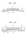
- FIGS. 10A through 10Eshow a method of manufacturing a chip scale package consistent with the present invention.
- a material for a lead frameis half-etched to have a predetermined section.
- a land 73is formed at the lead 72 through half-etching.
- the land 73is a portion exposed to the bottom surface of the encapsulation 75 of a package.
- the pad 71is half-etched along an edge side 71 a thereof, so that adhesion between the encapsulation resin and the pad 71 which are molded later is improved.
- the pad 71is connected to the lead 72 via the tie bar 81 and the support portion 83 in a state in which the half-etching process has been performed.
- plate layers 101 and 104are formed on the surfaces of the pad 71 and the lead 72 , respectively. Plating is performed with nickel, palladium, or silver.
- the lead 72is down-set processed.
- the pad 71is up-set processed. That is, the down-set portion 81 a of the tie bar 81 is bent by using a mold, as shown in FIG. 9.
- the pad 71 and the lead 72are positioned at different axial planes through the down-set or up-set process.
- the semiconductor chip 74is attached to the bottom surface of the pad 71 , and a wire-bonding step to connect the electrode of the semiconductor chip 74 and the lead 72 by a bonding wire 75 is performed.
- a ground wire 105is directly connected to the pad 71 so as to be electrically connected to the connection portion 81 b serving as a ground terminal via the tie bar as described above.
- the encapsulation 76is formed by molding the semiconductor chip 74 , the pad 71 , and the bonding wire 75 .
- the land 73 of the lead 72is molded to be exposed to the bottom surface of the encapsulation 76 , as described above.
- the upper surface of the pad 71may be formed near the surface of or exposed outside the encapsulation 76 .
- a heat sinkis attached to the upper surface of the pad 71 , so that the heat generated from the semiconductor chip 74 can be effectively dissipated.
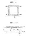
- FIG. 11shows the bottom surface of the semiconductor package manufactured as described above.
- a plurality of the leads 72are arranged around the bottom surface of the package which is rectangular.
- the connection portions 81 b of the tie bar functioning as the ground terminalare arranged at the four corners. As described above, the connection portions 81 b are connected to the pad 71 via the tie bar 81 which is not trimmed so that a predetermined ground function can be performed.
- the down-set method with respect to the tie bar 81has an important meaning when molding is performed and is one of various features of the present invention.
- the space for accommodating the lead frame where the semiconductor chip is mountedis formed inside the molding plate.
- the down-set processis performed such that t 1 ⁇ t 2 . That is, the entire height of the lead frame unit after the down-set process is performed must be formed to be greater than the thickness of the space in the molding plate.
- the upper surface of the pad 71 of FIG. 8is pressed against the inner surface of the upper plate and the bottom surface of the connection portion 81 b of the tie bar 81 is pressed against the inner surface of the lower plate. Also, the bottom surface of the lead 72 connected to the connection portion 81 b of the tie bar 81 via the support portion 83 is pressed against the inner surface of the lower plate.
- FIGS. 12A and 12Bshow a state in which the lead frame is pressed by the molding plate.
- the lead frameshave sections which are taken along line A-A of FIG. 9.
- FIG. 12Awhen an upper plate 111 and a lower plate are not pressed by a clamp (not shown), the entire height of a down-set processed lead frame is t 2 .
- the lead frameis disposed between the upper and lower plates 111 and 112 and receives clamping pressure P as shown in FIG. 12B.
- the depth of the space between the upper and lower plates 111 and 112becomes t 1 as shown in FIG. 12B because the lead frame is elastically deformed.
- the upper surface of the pad 71 and the connection portion 81 b of the tie bar 81are supported by being pressed against the inner surface of the upper plate 111 and the inner surface of the lower plate 112 , respectively.
- the bottom surface of the lead 72 connected to the tie bar 81 via the support portion 83is supported by being pressed by the inner surface of the lower plate ' 112 . In this state, when resin molding is performed, resin flows between the lead 72 and the lower plate 112 and between the pad 71 and the upper plate 111 , so that a flash phenomenon is prevented.
- FIG. 13shows a molding process, in which a matrix type lead frame unit on which semiconductor chips are mounted is accommodated in the molding plate.
- a lead frame on which the semiconductor chips 74 are mountedis accommodated in the space inside the molding plate including the upper and lower plates 111 and 112 .
- the pad 71 of the lead framecontacts the inner surface of the lower plate 112 with pressure.
- Molding resinis injected through a gate 115 of the molding plate and molding is performed. After the molding is performed, flash is removed, marking is performed, and dam bar is removed in a typical manner. Finally, the molding resin is severed so that individual semiconductor packages are obtained.
- FIG. 14A and 14Bshows a method of manufacturing a semiconductor package according to another embodiment consistent with the present invention.
- the semiconductor packageboth the lead and the pad are exposed to the bottom surface of the semiconductor package. Consequently, the semiconductor package has a cross section similar to that of the semiconductor package shown in FIG. 3.
- molding plates 121 a and 121 bare not pressed and, in such a state, a pad 122 on which a semiconductor chip 127 is mounted is down-set processed at a position lower than a lead 123 . That is, when the lead frame is down-set processed, the height of the pad 122 is set to be lower than that of the lead 123 .
- Reference numeral 125denotes a bonding wire.
- FIG. 14Bshows a state in which molding resin 126 is injected when the molding plates 121 a and 121 b are clamped.
- the lead frame accommodated between the molding plates 121 a and 121 breceives a clamping pressure indicated by P.
- the pad 122contacts the inner surface of the lower plate 121 a with pressure, so that a flash phenomenon can be prevented.
- the method for manufacturing a semiconductor package described with reference to FIGS. 14A and 14Bis preferably applied to the case in which the lead frame is individually molded. That is, it is preferable to perform the method shown in FIGS. 14A and 14B for the lead frame unit shown in FIG. 4, rather than for the matrix type lead frame unit shown in FIG. 5. However, the lead frame unit shown in FIG. 5 is more preferable than that shown in FIG. 4 in view of manufacturing cost and process.
- FIG. 15shows the method of manufacturing a semiconductor package described with reference to FIGS. 14A and 14B.
- a tie bar 137extends from a pad 122 on which a semiconductor chip 127 is mounted.
- the tie bar 137 and the lead 123are connected by a support portion 139 .
- the support portion 139 and the lead 123are disposed on the same plane and the pad 122 is down-set processed at an axial plane different from a plane of the support portion 139 and the lead 123 .
- a bonding wireis not shown for the convenience of illustration.
- the pad and the tie bar extending from the padare down-set or up-set processed to be placed on different planes, a flash phenomenon that can be generated in the molding plate during the encapsulation step is prevented.
- the semiconductor package manufacturing method incorporating a matrix type lead frame unitcan be utilized without adverse effects caused by the flash phenomenon. Also, reliability in manufacture of semiconductor packages is improved. Furthermore, high productivity at a lower manufacturing cost can be expected.
Landscapes
- Physics & Mathematics (AREA)
- Engineering & Computer Science (AREA)
- Condensed Matter Physics & Semiconductors (AREA)
- General Physics & Mathematics (AREA)
- Computer Hardware Design (AREA)
- Microelectronics & Electronic Packaging (AREA)
- Power Engineering (AREA)
- Geometry (AREA)
- Manufacturing & Machinery (AREA)
- Encapsulation Of And Coatings For Semiconductor Or Solid State Devices (AREA)
- Structures Or Materials For Encapsulating Or Coating Semiconductor Devices Or Solid State Devices (AREA)
- Lead Frames For Integrated Circuits (AREA)
Abstract
Description
- 1. Field of the Invention[0001]
- The present invention relates to a lead frame, a semiconductor package having the lead frame, and a method for manufacturing the semiconductor package, and more particularly, to a lead frame in which a flash phenomenon occurring to molding resin in a semiconductor package can be prevented, a semiconductor package having the lead frame, and a method for manufacturing the semiconductor package.[0002]
- 2. Description of the Related Art[0003]
- In general, a semiconductor package is formed by arranging a semiconductor chip on a pad of a lead frame, wire-bonding an electrode of the semiconductor chip and an inner lead of the lead frame, and encapsulating the pad and the inner lead frame with molding resin.[0004]
- Recently, the capacity of a semiconductor package becomes large while the size thereof is reduced. For example, a chip scale package (CSP) is developed. While leads protrude from the side surface of a semiconductor package in the conventional semiconductor package, in the chip scale package, leads protrude from the bottom surface of the semiconductor package. If the leads protrude from the bottom surface of the semiconductor package, the size of the package drastically decreases and a space occupied by the package is further reduced. To expose leads to the bottom surface of the package, the leads need to be down-set or half-etched. The exposed leads contact terminals on a printed circuit board. In some particular cases, a pad on which a semiconductor chip is arranged is exposed to the bottom surface of the package.[0005]
- FIG. 1 is a sectional view of a semiconductor package according to a conventional technology, which is disclosed in Japanese Patent Publication No. 59-21047. Referring to the drawing, a[0006]
semiconductor chip 14 is mounted on the upper surface of apad 11 and alead 12 is down-set processed. Abottom surface 12aof thelead 12 is exposed to the bottom surface of anencapsulation 15 so that thelead 12 can contact a connection terminal (not shown) on a printed circuit board. An upper end of thelead 12 and an electrode (not shown) of thesemiconductor chip 14 are connected by abonding wire 13. Thepad 11 is positioned lower than the upper end of thelead 12. The semiconductor package of FIG. 1 is a typical example in which thelead 12 is down-set processed. - FIG. 2 shows another example of a semiconductor package according to the conventional technology, which is disclosed in Japanese Patent Publication No. 59-227143. Referring to the drawing, a[0007]
semiconductor chip 24 is mounted on apad 21. Alead 22 is processed by a half-etching method so that abottom surface 22athereof is exposed to the bottom surface of anencapsulation 25. One end of thelead 22 and an electrode of thesemiconductor chip 24 are connected by abonding wire 23. The semiconductor package of FIG. 2 is an example in whichlead 22 is half-etched. - FIG. 3 shows yet another example of a semiconductor package according to a conventional technology, which is disclosed in U.S. Pat. No. 6,143,981. Referring to the drawing, a[0008]
semiconductor chip 34 is mounted on an upper surface of apad 31. A bottom surface of thepad 31 and abottom surface 32aof alead 32 are exposed from the bottom surface of anencapsulation 35. That is, thepad 31 and thelead 32 are formed at the same height. Thelead 32 and electrodes of thesemiconductor chip 34 are connected by abonding wire 33. The exposedlead 32 contacts a connection terminal on a printed circuit board. The bottom surface of the exposedpad 31 radiates heat generated by thesemiconductor chip 34 to the outside. The exposedpad 31 is connected to a thermal pad (not shown) on the printed circuit board. The semiconductor package of FIG. 3 is an example in which thepad 31 is exposed to the outside. - When a semiconductor package described with reference to FIG. 3 is to be manufactured, there are typically two conventional manufacturing methods that can be applied. In the first method, there is a lead frame unit including a[0009]
separate lead frame 41 and arail 42 encompassing thelead frame 41 from the outside, as shown in FIG. 4. The lead frame unit undergoes wafer sawing, die attach, wire bonding, molding/deflashing, marking, and trimming/forming. The merit of using a lead frame to which trimming is applied individually is that generation of flash to mold is relatively restricted. However, complete prevention of the flash generation is not possible so that an additional step of removing the flash is actually needed. - In the second method, a lead frame is not individually trimmed, but a lead frame unit in which a plurality of lead frames are arranged in form of matrix is molded together. The lead frame unit in form of matrix is shown in FIG. 5. Here,[0010]
reference numeral 51 denotes an individual lead frame andreference numeral 52 denotes a rail encompassing each lead frame from the outside. The matrix type lead frame unit is assembled by steps of wafer sawing, die attach, wire bonding, molding/deflashing, marking, and singulation by sawing. - In the above-described two semiconductor package assembly processes, the individually trimmed lead frame has smaller unit density per unit area because the unit area on a lead frame strip is greater than the unit area of the matrix type. Thus, a unit price per unit area increases. To reduce the disadvantage, the matrix type lead frame is more frequently used. However, when a semiconductor package where a pad is exposed to the bottom surface of the package is molded in a matrix form, mold flash can be generated in a molding step such that application of a matrix type lead frame is not possible.[0011]
- FIG. 6 shows a molding step of a semiconductor package which corresponds to a molding step using a matrix type lead frame. Referring to the drawing, molding of a semiconductor package is formed in a molding plate including an[0012]
upper plate 61 and alower plate 62. A space, in which a lead frame connected to a chip by wire bonding is placed, is formed between the upper andlower plates molding resin 64. Themolding resin 64 may be injected into the space through agate 63. The lead frame is provided with apad 65 and alead 67 and asemiconductor chip 66 is mounted on the upper surface of thepad 65. An electrode of thesemiconductor chip 66 and thelead 67 are connected by abonding wire 68. The lead frame is of a matrix type shown in FIG. 5, which has not cut yet into individual lead frames. - When an encapsulation step is actually performed by using the molding plate shown in FIG. 6, mold flash is generated between the bottom surfaces of the[0013]
pad 65 and thelead 67 and the inner surface of thelower plate 62. This is because the lead frame is twisted due to thermal expansion as temperature increases in the state in which the lead frame unit is accommodated inside the molding plate. Also, since theupper plate 61 clamps only the edge of the lead frame unit, the central portion except for the edge portion is not clamped so that the lead frame unit is lifted and molding resin intrudes under the lead or the pad, generating flash. - To prevent a flash phenomenon during molding, a method using a rear side tape is introduced. That is, a heat-resistant tape such as polyimide or Teflon is laminated on the rear side of the lead frame. Since an adhesive layer is present on the polyimide tape, the polyimide tape is attached to the inner surface of the lower plate so that generation of flash can be prevented. However, since the method using the rear side tape uses a special tape of a particular company, cost is high and an additional step is needed, increasing an investment cost. Also, after the tape is removed, the adhesive remains on the surface of the lead frame so that a degree of welding is lowered. To remove the adhesive, a chemical process is required.[0014]
- To solve the above-described problems, it is an object of the present invention to provide an improved lead frame in which a mold flash phenomenon is prevented.[0015]
- It is another objective of the present invention to provide an improved semiconductor package in which a flash phenomenon and a boundary surface separation phenomenon are prevented.[0016]
- It is yet another objective of the present invention to provide an improved semiconductor package manufacturing method by which the flash phenomenon and the boundary surface separation phenomenon are prevented.[0017]
- It is another objective of the present invention to provide a semiconductor package which is assembled by an assembly step which is the same as or similar to the conventional semiconductor package assembly step, a lead frame needed therefore, and an improved manufacturing method.[0018]
- To achieve the above objectives, there is provided a lead frame for an encapsulated semiconductor package having a predetermined thickness, comprising a pad for receiving a semiconductor chip, the pad having a top surface, a support portion having a bottom surface and a plurality of leads formed on the support portion, a resilient tie bar having a first end connected to the pad and a second end connected to the support portion, the tie bar when in an unstressed condition supporting the pad such that the top surface of the pad and the bottom surface of the supporting portion and leads are separated by a distance greater than the predetermined thickness.[0019]
- It is preferred that the tie bar is down-set processed.[0020]
- It is preferred that at least a portion of the plurality of leads is half-etched.[0021]
- It is preferred that the half-etched portion is electrically connected to the semiconductor chip.[0022]
- It is preferred that the lead frame when in a stressed condition is configured to fit into a space defined by a pair of molding plates separated by a distance of the predetermined thickness.[0023]
- To achieve the above objectives, there is provided an encapsulated semiconductor package having a predetermined thickness, comprising a pad having a first surface and a second surface opposite to the first surface, a support portion having a bottom surface and a plurality of leads formed on the support portion, a semiconductor chip attached to the first surface of the pad, a resilient tie bar having a first end connected to the pad and a second end connected to the support portion, and an encapsulation having a first surface and a second surface opposite to the first surface, the second surface of the pad being exposed to the first surface of the encapsulation and the leads being exposed to the second surface of the encapsulation.[0024]
- It is preferred that the second surface of the pad and the bottom surface of the support portion are separated by a predetermined distance.[0025]
- It is preferred that the predetermined distance prior to forming the encapsulation is greater than the predetermined thickness.[0026]
- It is preferred that the encapsulated semiconductor package comprises at least one bonding wire connected between an electrode of the semiconductor chip and each of the plurality of leads.[0027]
- It is preferred that the resilient tie bar is down-set processed.[0028]
- It is preferred that the pad and the support portion when in a stressed condition are configured to fit into a space defined by a pair of molding plates separated by a distance of the predetermined thickness.[0029]
- It is preferred that the first surface of the pad is the bottom surface of the pad and the second surface of the pad is the upper surface of the pad, and that the first surface of the encapsulation is the upper surface of the encapsulation and the second surface of the encapsulation is the bottom surface of the encapsulation.[0030]
- It is preferred that the first surface of the pad is the upper surface of the pad and the second surface of the pad is the bottom surface of the pad, and that the first surface of the encapsulation is the bottom surface of the encapsulation and the second surface of the encapsulation is the upper surface of the encapsulation.[0031]
- It is preferred that at least a portion of the plurality of leads is half-etched.[0032]
- It is preferred that the half-etched portion is electrically connected to the semiconductor chip.[0033]
- To achieve the above objectives, there is provided a method of manufacturing a semiconductor package, comprising providing a lead frame comprising a pad, a plurality of leads, and a tie bar extending from the pad and supporting the pad, down-set processing the tie bar so that the pad and the leads are disposed on different axial planes with a predetermined distance from each other, deforming the lead frame by providing a pair of molding plates on opposite sides of the lead frame and separated from each other by a predetermined thickness for forming an encapsulation, the predetermined thickness being less than a sum of the predetermined distance, a thickness of the pad, a thickness of the lead, and injecting a molding resin between the molding plates to form an encapsulated package.[0034]
- It is preferred that the method comprises a step of half-etching at least a portion of the leads.[0035]
- It is preferred that the method comprises a step of electrically connecting the half-etched portion to a semiconductor chip.[0036]
- It is preferred that the method comprises attaching a semiconductor chip to one surface of the pad.[0037]
- It is preferred that the method comprises connecting an electrode of the semiconductor chip and the leads by a bonding wire.[0038]
- It is preferred that the method comprises accommodating the lead frame in the inside space between the pair of molding plates, pressing the pad which makes a contact with a surface of one of the molding plates, and injecting the molding resin into the inside space while pressing the pad, thus forming the encapsulation.[0039]
- It is preferred that the method comprises cutting a portion connecting to the leads.[0040]
- It is preferred that the semiconductor chip is attached to a bottom surface of the pad.[0041]
- It is preferred that the semiconductor chip is attached to the upper surface of the pad.[0042]
- It is preferred that the lead frame is provided as a lead frame unit where a plurality of lead frames are connected in a matrix format.[0043]
- It is preferred that the lead frame is an individually molded and trimmed lead frame.[0044]
- It is preferred that the plurality of leads are formed on a support portion, the support portion connected to the tie bar for providing a support for the pad.[0045]
- It is to be understood that both the foregoing general description and the following detailed description are exemplary and explanatory only and are not restrictive of the invention, as claimed.[0046]
- The above objectives and advantages of the present invention will become more apparent by describing in detail preferred embodiments thereof with reference to the attached drawings in which:[0047]
- FIG. 1 is a sectional view showing a conventional semiconductor package;[0048]
- FIG. 2 is a sectional view showing another conventional semiconductor package;[0049]
- FIG. 3 is a sectional view showing yet another conventional semiconductor package;[0050]
- FIG. 4 is a plan view showing a strip of a lead frame unit which is individually trimmed after being resin molded;[0051]
- FIG,[0052]5 is a plan view showing a strip of a matrix type lead frame unit;
- FIG. 6 is a sectional view showing a method of molding a semiconductor package according to a conventional technology, in which a matrix type lead frame unit is applied;[0053]
- FIG. 7 is a sectional view showing a semiconductor package according to an embodiment consistent with the present invention;[0054]
- FIG. 8 is a perspective view showing a lead frame used for forming the semiconductor package of FIG. 7;[0055]
- FIG. 9 is a plan view showing the lead frame of FIG. 8;[0056]
- FIGS. 10A through 10E are views showing a method of manufacturing a semiconductor package consistent with the present invention;[0057]
- FIG. 11 is a bottom view of a completed semiconductor package;[0058]
- FIGS. 12A and 12B are sectional views for explaining a state in which the lead frame is pressed by the molding plate;[0059]
- FIG. 13 is a sectional view for explaining a molding step in which a matrix type lead frame unit on which the semiconductor chip is mounted is accommodated in the molding plate;[0060]
- FIGS. 14A and 14B are sectional views for explaining a method of manufacturing a semiconductor package according to another embodiment consistent with the present invention; and[0061]
- FIG. 15 is an exploded perspective view showing a method of manufacturing the semiconductor package described with reference to FIGS. 14A and 14B.[0062]
- Reference will now be made in detail to exemplary embodiments consistent with the invention, examples of which are illustrated in the accompanying drawings. Wherever possible, the same reference numbers will be used throughout the drawings to refer to the same or like parts.[0063]
- Referring to FIG. 7, in a semiconductor package according to an embodiment consistent with the present invention, a[0064]
semiconductor chip 74 is attached to the bottom surface of apad 71. A lead72 is arranged at a height different from thepad 71. Thepad 71 and thelead 72 can receive a predetermined process by half-etching and are plated with noble metal such as silver or palladium. Thelead 72 and thesemiconductor chip 74 are connected by abonding wire 75. Thepad 71, thelead 72, and thesemiconductor chip 74 are encompassed by anencapsulation 76. A tie bar which is not shown in the drawing has one end connected to the edge of thepad 71 and extending therefrom and the other end thereof extending to the same height as thelead 72. The tie bar is down-set processed and will be described in detail later. - In the semiconductor package as shown in FIG. 7, the upper surface of the[0065]
pad 71 is exposed to the upper surface of theencapsulation 76 and the bottom surface of thelead 72 is exposed to the bottom surface of theencapsulation 76. The bottom surface of the exposedlead 72 contacts a connection terminal of a printed circuit board to form an electrical connection circuit. The upper surface of the exposedpad 71 may help dissipate the heat generated from thesemiconductor chip 74 to the outside. - FIG. 8 shows a lead frame used in the semiconductor package shown in FIG. 7. FIG. 9 is a plan view of the lead frame of FIG. 8. Referring to the drawings, a[0066]
tie bar 81 extends from the edge of thepad 71 and a plurality of theleads 72 are arranged around thepad 71. As described above, thepad 71 and thelead 72 are arranged at different axial planes. This is because thetie bar 81 supports thepad 71 at a higher plane than the plane of thelead 72. That is, as a particular portion of thetie bar 81 is down-set processed, thepad 71 may be maintained at a different axial plane with respect to the plane of thelead 72.Reference numeral 81 a denotes a portion of thetie bar 81 which is down-set processed.Reference numeral 81bdenotes a connection portion of thetie bar 81 connected to thelead 72 and supporting thepad 71 at a different axial plane. Theconnection portion 81band thelead 72 are arranged on the same axial plane. Thetie bar 81 and thelead 72 are connected via asupport portion 83. - A plurality of the above-described lead frames shown in FIGS. 8 and 9 are connected in a matrix format, thus forming a lead frame unit as shown in FIG. 5. Actually, prior to performing a down-set process, the[0067]
pad 71, thelead 72 and thetie bar 81 are formed by means of punching, etching or stamping. The down-set process is performed by a mold such that thetie bar 81 supports thepad 71 as shown in FIG. 8. Thesupport portion 83 connecting thelead 72 can be removed usually after molding is performed. - Hereinafter, a method of manufacturing a semiconductor package consistent with the present invention will now be described.[0068]
- A lead frame used in a semiconductor package consistent with the present invention may be manufactured in a typical method. That is, the pad, lead, and tie bar are formed by etching or stamping, and at least an inner lead portion or a pad portion to be wire-bonded is plated with silver or palladium. The thickness and type of plating differs based on the purpose of a product. Recently, PPF plating using a nickel/palladium material is primarily applied. After the lead frame is manufactured, a down-set process is performed in a mechanical manner. That is, as shown in FIG. 8, the[0069]
tie bar 81 is plastically deformed so that thetie bar 81 supports the lead portion and thepad 71 at different planes. - FIGS. 10A through 10E show a method of manufacturing a chip scale package consistent with the present invention. Referring to FIG. 10A, a material for a lead frame is half-etched to have a predetermined section. A[0070]
land 73 is formed at thelead 72 through half-etching. Theland 73 is a portion exposed to the bottom surface of theencapsulation 75 of a package. Also, thepad 71 is half-etched along anedge side 71athereof, so that adhesion between the encapsulation resin and thepad 71 which are molded later is improved. - As described in FIG. 9, the[0071]
pad 71 is connected to thelead 72 via thetie bar 81 and thesupport portion 83 in a state in which the half-etching process has been performed. - Referring to FIG. 10B, plate layers[0072]101 and104 are formed on the surfaces of the
pad 71 and thelead 72, respectively. Plating is performed with nickel, palladium, or silver. - Referring to FIG. 10C, the[0073]
lead 72 is down-set processed. The same result may be obtained if thepad 71 is up-set processed. That is, the down-setportion 81aof thetie bar 81 is bent by using a mold, as shown in FIG. 9. Thus, thepad 71 and thelead 72 are positioned at different axial planes through the down-set or up-set process. - Referring to FIG. 10D, the[0074]
semiconductor chip 74 is attached to the bottom surface of thepad 71, and a wire-bonding step to connect the electrode of thesemiconductor chip 74 and thelead 72 by abonding wire 75 is performed. Aground wire 105 is directly connected to thepad 71 so as to be electrically connected to theconnection portion 81bserving as a ground terminal via the tie bar as described above. - Referring to FIG. 10E, the[0075]
encapsulation 76 is formed by molding thesemiconductor chip 74, thepad 71, and thebonding wire 75. Theland 73 of thelead 72 is molded to be exposed to the bottom surface of theencapsulation 76, as described above. The upper surface of thepad 71 may be formed near the surface of or exposed outside theencapsulation 76. Although not shown in the drawing, a heat sink is attached to the upper surface of thepad 71, so that the heat generated from thesemiconductor chip 74 can be effectively dissipated. - FIG. 11 shows the bottom surface of the semiconductor package manufactured as described above. Referring to the drawing, a plurality of the[0076]
leads 72 are arranged around the bottom surface of the package which is rectangular. Theconnection portions 81bof the tie bar functioning as the ground terminal are arranged at the four corners. As described above, theconnection portions 81bare connected to thepad 71 via thetie bar 81 which is not trimmed so that a predetermined ground function can be performed. - The down-set method with respect to the[0077]
tie bar 81 has an important meaning when molding is performed and is one of various features of the present invention. As described in the above with reference to FIG. 6, the space for accommodating the lead frame where the semiconductor chip is mounted is formed inside the molding plate. When the thickness of the space in the molding plate is t1 and the entire height of the lead frame unit after the down-set process is performed is t2, the down-set process is performed such that t1<t2. That is, the entire height of the lead frame unit after the down-set process is performed must be formed to be greater than the thickness of the space in the molding plate. Thus, while molding is performed in the state in which the upper and lower plates of the molding plate are clamped each other, the upper surface of thepad 71 of FIG. 8 is pressed against the inner surface of the upper plate and the bottom surface of theconnection portion 81bof thetie bar 81 is pressed against the inner surface of the lower plate. Also, the bottom surface of thelead 72 connected to theconnection portion 81bof thetie bar 81 via thesupport portion 83 is pressed against the inner surface of the lower plate. - FIGS. 12A and 12B show a state in which the lead frame is pressed by the molding plate. In the drawings, the lead frames have sections which are taken along line A-A of FIG. 9. In FIG. 12A, when an[0078]
upper plate 111 and a lower plate are not pressed by a clamp (not shown), the entire height of a down-set processed lead frame is t2. - The lead frame is disposed between the upper and[0079]
lower plates lower plates pad 71 and theconnection portion 81bof thetie bar 81 are supported by being pressed against the inner surface of theupper plate 111 and the inner surface of thelower plate 112, respectively. Also, the bottom surface of thelead 72 connected to thetie bar 81 via thesupport portion 83 is supported by being pressed by the inner surface of the lower plate '112. In this state, when resin molding is performed, resin flows between the lead72 and thelower plate 112 and between thepad 71 and theupper plate 111, so that a flash phenomenon is prevented. - FIG. 13 shows a molding process, in which a matrix type lead frame unit on which semiconductor chips are mounted is accommodated in the molding plate. Referring to the drawing, a lead frame on which the semiconductor chips[0080]74 are mounted is accommodated in the space inside the molding plate including the upper and
lower plates pad 71 of the lead frame contacts the inner surface of thelower plate 112 with pressure. Molding resin is injected through agate 115 of the molding plate and molding is performed. After the molding is performed, flash is removed, marking is performed, and dam bar is removed in a typical manner. Finally, the molding resin is severed so that individual semiconductor packages are obtained. - FIGS. 14A and 14B shows a method of manufacturing a semiconductor package according to another embodiment consistent with the present invention. In the semiconductor package, both the lead and the pad are exposed to the bottom surface of the semiconductor package. Consequently, the semiconductor package has a cross section similar to that of the semiconductor package shown in FIG. 3.[0081]
- Referring to FIG. 14A,[0082]
molding plates pad 122 on which asemiconductor chip 127 is mounted is down-set processed at a position lower than alead 123. That is, when the lead frame is down-set processed, the height of thepad 122 is set to be lower than that of thelead 123.Reference numeral 125 denotes a bonding wire. - FIG. 14B shows a state in which[0083]
molding resin 126 is injected when themolding plates molding plates pad 122 contacts the inner surface of thelower plate 121awith pressure, so that a flash phenomenon can be prevented. - Actually, the method for manufacturing a semiconductor package described with reference to FIGS. 14A and 14B is preferably applied to the case in which the lead frame is individually molded. That is, it is preferable to perform the method shown in FIGS. 14A and 14B for the lead frame unit shown in FIG. 4, rather than for the matrix type lead frame unit shown in FIG. 5. However, the lead frame unit shown in FIG. 5 is more preferable than that shown in FIG. 4 in view of manufacturing cost and process.[0084]
- FIG. 15 shows the method of manufacturing a semiconductor package described with reference to FIGS. 14A and 14B. Referring to the drawing, a[0085]
tie bar 137 extends from apad 122 on which asemiconductor chip 127 is mounted. Thetie bar 137 and thelead 123 are connected by asupport portion 139. Thesupport portion 139 and thelead 123 are disposed on the same plane and thepad 122 is down-set processed at an axial plane different from a plane of thesupport portion 139 and thelead 123. Here, a bonding wire is not shown for the convenience of illustration. When theupper plate 121bof the molding plate covers over thelower plate 121a,anouter portion 132 of theupper plate 121bfor forming an inner space clamps thelead 123 and thesupport portion 139. Here, since thepad 122 is down-set processed at a position lower than the plane of thelead 123 and thesupport portion 139, when thelead 123 and thesupport portion 139 are clamped, the bottom surface of thepad 122 contacts the upper surface of thelower plate 121awith pressure. Thus, when molding resin is injected into the space formed inside the molding plate, possibility of flash generation between the bottom surface of thepad 122 and the upper surface of thelower plate 121ais prevented. - As described above, in the lead frame consistent with the present invention, since the pad and the tie bar extending from the pad are down-set or up-set processed to be placed on different planes, a flash phenomenon that can be generated in the molding plate during the encapsulation step is prevented. Thus, the semiconductor package manufacturing method incorporating a matrix type lead frame unit can be utilized without adverse effects caused by the flash phenomenon. Also, reliability in manufacture of semiconductor packages is improved. Furthermore, high productivity at a lower manufacturing cost can be expected.[0086]
- While this invention has been particularly shown and described with reference to exemplary embodiments thereof, it will be understood by those skilled in the art that various changes in form and details may be made therein without departing from the spirit and scope of the invention as defined by the appended claims.[0087]
Claims (27)
1. A lead frame for an encapsulated semiconductor package having a predetermined thickness, comprising:
a pad for receiving a semiconductor chip, the pad having a top surface;
a support portion having a bottom surface and a plurality of leads formed on the support portion;
a resilient tie bar having a first end connected to the pad and a second end connected to the support portion, the tie bar when in an unstressed condition supporting the pad such that the top surface of the pad and the bottom surface of the supporting portion and leads are separated by a distance greater than the predetermined thickness.
2. The lead frame as claimed inclaim 1 , wherein the tie bar is down-set processed.
3. The lead frame as claimed inclaim 1 , wherein at least a portion of the plurality of leads is half-etched.
4. The lead frame as claimed inclaim 3 , wherein the half-etched portion is electrically connected to the semiconductor chip.
5. The lead frame as claimed inclaim 1 , wherein the lead frame when in a stressed condition is configured to fit into a space defined by a pair of molding plates separated by a distance of the predetermined thickness.
6. An encapsulated semiconductor package having a predetermined thickness, comprising:
a pad having a first surface and a second surface opposite to the first surface;
a support portion having a bottom surface and a plurality of leads formed on the support portion;
a semiconductor chip attached to the first surface of the pad;
a resilient tie bar having a first end connected to the pad and a second end connected to the support portion; and
an encapsulation having a first surface and a second surface opposite to the first surface;
the second surface of the pad being exposed to the first surface of the encapsulation and the leads being exposed to the second surface of the encapsulation.
7. The encapsulated semiconductor package as claimed inclaim 6 , wherein the second surface of the pad and the bottom surface of the support portion are separated by a predetermined distance.
8. The encapsulated semiconductor package as claimed inclaim 7 , wherein the predetermined distance prior to forming the encapsulation is greater than the predetermined thickness.
9. The encapsulated semiconductor package as claimed inclaim 6 , comprising at least one bonding wire connected between an electrode of the semiconductor chip and each of the plurality of leads.
10. The encapsulated semiconductor package as claimed inclaim 6 , wherein the resilient tie bar is down-set processed.
11. The encapsulated semiconductor package as claimed inclaim 6 , wherein the pad and the support portion when in a stressed condition are configured to fit into a space defined by a pair of molding plates separated by a distance of the predetermined thickness.
12. The encapsulated semiconductor package as claimed inclaim 6 , wherein:
the first surface of the pad is the bottom surface of the pad and the second surface of the pad is the upper surface of the pad; and
the first surface of the encapsulation is the upper surface of the encapsulation and the second surface of the encapsulation is the bottom surface of the encapsulation.
13. The encapsulated semiconductor package as claimed inclaim 6 , wherein:
the first surface of the pad is the upper surface of the pad and the second surface of the pad is the bottom surface of the pad; and
the first surface of the encapsulation is the bottom surface of the encapsulation and the second surface of the encapsulation is the upper surface of the encapsulation.
14. The encapsulated semiconductor package as claimed inclaim 6 , wherein at least a portion of the plurality of leads is half-etched.
15. The encapsulated semiconductor package as claimed inclaim 14 , wherein the half-etched portion is electrically connected to the semiconductor chip.
16. A method of manufacturing a semiconductor package, comprising:
providing a lead frame comprising:
a pad,
a plurality of leads, and
a tie bar extending from the pad and supporting the pad;
down-set processing the tie bar so that the pad and the leads are disposed on different axial planes with a predetermined distance from each other;
deforming the lead frame by providing a pair of molding plates on opposite sides of the lead frame and separated from each other by a predetermined thickness for forming an encapsulation, the predetermined thickness being less than a sum of the predetermined distance, a thickness of the pad, a thickness of the lead; and
injecting a molding resin between the molding plates to form an encapsulated package.
17. The method as claimed inclaim 16 , comprising a step of half-etching at least a portion of the leads.
18. The method as claimed inclaim 17 , comprising a step of electrically connecting the half-etched portion to a semiconductor chip.
19. The method as claimed inclaim 16 , comprising attaching a semiconductor chip to one surface of the pad.
20. The method as claimed inclaim 19 , comprising connecting an electrode of the semiconductor chip and the leads by a bonding wire.
21. The method as claimed inclaim 19 , comprising:
accommodating the lead frame in the inside space between the pair of molding plates, pressing the pad which makes a contact with a surface of one of the molding plates; and
injecting the molding resin into the inside space while pressing the pad, thus forming the encapsulation.
22. The method as claimed inclaim 21 , comprising cutting a portion connecting to the leads.
23. The method as claimed inclaim 19 , wherein the semiconductor chip is attached to a bottom surface of the pad.
24. The method as claimed inclaim 19 , wherein the semiconductor chip is attached to the upper surface of the pad.
25. The method as claimed inclaim 16 , wherein the lead frame is provided as a lead frame unit where a plurality of lead frames are connected in a matrix format.
26. The method as claimed inclaim 16 , wherein the lead frame is an individually molded and trimmed lead frame.
27. The method as claimed inclaim 16 , wherein the plurality of leads are formed on a support portion, the support portion connected to the tie bar for providing a support for the pad.
Priority Applications (1)
| Application Number | Priority Date | Filing Date | Title |
|---|---|---|---|
| US10/262,848US20030030131A1 (en) | 2000-09-15 | 2002-10-03 | Semiconductor package apparatus and method |
Applications Claiming Priority (6)
| Application Number | Priority Date | Filing Date | Title |
|---|---|---|---|
| KR2000-54200 | 2000-09-15 | ||
| KR1020000054200AKR20020021476A (en) | 2000-09-15 | 2000-09-15 | Chip scale semiconductor package and manufacturing method therefor |
| KR1020010042344AKR20030006532A (en) | 2001-07-13 | 2001-07-13 | Lead Frame, Semi-conductor Package therewith and Method for manufacturing Semi-Conductor Package |
| KR2001-42344 | 2001-07-13 | ||
| US09/953,195US20020037604A1 (en) | 2000-09-15 | 2001-09-17 | Lead frame, semiconductor package having lead frame, and method of manufacturing semiconductor package |
| US10/262,848US20030030131A1 (en) | 2000-09-15 | 2002-10-03 | Semiconductor package apparatus and method |
Related Parent Applications (1)
| Application Number | Title | Priority Date | Filing Date |
|---|---|---|---|
| US09/953,195DivisionUS20020037604A1 (en) | 2000-09-15 | 2001-09-17 | Lead frame, semiconductor package having lead frame, and method of manufacturing semiconductor package |
Publications (1)
| Publication Number | Publication Date |
|---|---|
| US20030030131A1true US20030030131A1 (en) | 2003-02-13 |
Family
ID=26638387
Family Applications (2)
| Application Number | Title | Priority Date | Filing Date |
|---|---|---|---|
| US09/953,195AbandonedUS20020037604A1 (en) | 2000-09-15 | 2001-09-17 | Lead frame, semiconductor package having lead frame, and method of manufacturing semiconductor package |
| US10/262,848AbandonedUS20030030131A1 (en) | 2000-09-15 | 2002-10-03 | Semiconductor package apparatus and method |
Family Applications Before (1)
| Application Number | Title | Priority Date | Filing Date |
|---|---|---|---|
| US09/953,195AbandonedUS20020037604A1 (en) | 2000-09-15 | 2001-09-17 | Lead frame, semiconductor package having lead frame, and method of manufacturing semiconductor package |
Country Status (5)
| Country | Link |
|---|---|
| US (2) | US20020037604A1 (en) |
| JP (1) | JP2002134676A (en) |
| CN (1) | CN1210793C (en) |
| SG (1) | SG102638A1 (en) |
| TW (1) | TW508774B (en) |
Cited By (95)
| Publication number | Priority date | Publication date | Assignee | Title |
|---|---|---|---|---|
| US20040065905A1 (en)* | 2001-03-27 | 2004-04-08 | Jong Sik Paek | Semiconductor package and method for manufacturing the same |
| US6844615B1 (en) | 2003-03-13 | 2005-01-18 | Amkor Technology, Inc. | Leadframe package for semiconductor devices |
| US6873041B1 (en) | 2001-11-07 | 2005-03-29 | Amkor Technology, Inc. | Power semiconductor package with strap |
| US6893900B1 (en) | 1998-06-24 | 2005-05-17 | Amkor Technology, Inc. | Method of making an integrated circuit package |
| US6921967B2 (en) | 2003-09-24 | 2005-07-26 | Amkor Technology, Inc. | Reinforced die pad support structure |
| US6953988B2 (en) | 2000-03-25 | 2005-10-11 | Amkor Technology, Inc. | Semiconductor package |
| US6965157B1 (en) | 1999-11-09 | 2005-11-15 | Amkor Technology, Inc. | Semiconductor package with exposed die pad and body-locking leadframe |
| US6967395B1 (en) | 2001-03-20 | 2005-11-22 | Amkor Technology, Inc. | Mounting for a package containing a chip |
| US6995459B2 (en) | 2002-09-09 | 2006-02-07 | Amkor Technology, Inc. | Semiconductor package with increased number of input and output pins |
| US6998702B1 (en) | 2001-09-19 | 2006-02-14 | Amkor Technology, Inc. | Front edge chamfer feature for fully-molded memory cards |
| US7001799B1 (en) | 2003-03-13 | 2006-02-21 | Amkor Technology, Inc. | Method of making a leadframe for semiconductor devices |
| US7005326B1 (en) | 1998-06-24 | 2006-02-28 | Amkor Technology, Inc. | Method of making an integrated circuit package |
| US7008825B1 (en)* | 2003-05-27 | 2006-03-07 | Amkor Technology, Inc. | Leadframe strip having enhanced testability |
| US7030474B1 (en) | 1998-06-24 | 2006-04-18 | Amkor Technology, Inc. | Plastic integrated circuit package and method and leadframe for making the package |
| US7045883B1 (en) | 2001-04-04 | 2006-05-16 | Amkor Technology, Inc. | Thermally enhanced chip scale lead on chip semiconductor package and method of making same |
| US7045882B2 (en) | 2000-12-29 | 2006-05-16 | Amkor Technology, Inc. | Semiconductor package including flip chip |
| US7057268B1 (en) | 2004-01-27 | 2006-06-06 | Amkor Technology, Inc. | Cavity case with clip/plug for use on multi-media card |
| US7057280B2 (en) | 1998-11-20 | 2006-06-06 | Amkor Technology, Inc. | Leadframe having lead locks to secure leads to encapsulant |
| US7064009B1 (en) | 2001-04-04 | 2006-06-20 | Amkor Technology, Inc. | Thermally enhanced chip scale lead on chip semiconductor package and method of making same |
| US7067908B2 (en) | 1999-10-15 | 2006-06-27 | Amkor Technology, Inc. | Semiconductor package having improved adhesiveness and ground bonding |
| US7071541B1 (en) | 1998-06-24 | 2006-07-04 | Amkor Technology, Inc. | Plastic integrated circuit package and method and leadframe for making the package |
| US7091594B1 (en) | 2004-01-28 | 2006-08-15 | Amkor Technology, Inc. | Leadframe type semiconductor package having reduced inductance and its manufacturing method |
| US7112474B1 (en) | 1998-06-24 | 2006-09-26 | Amkor Technology, Inc. | Method of making an integrated circuit package |
| US7115445B2 (en) | 1999-10-15 | 2006-10-03 | Amkor Technology, Inc. | Semiconductor package having reduced thickness |
| US7138707B1 (en) | 2003-10-21 | 2006-11-21 | Amkor Technology, Inc. | Semiconductor package including leads and conductive posts for providing increased functionality |
| US7144517B1 (en) | 2003-11-07 | 2006-12-05 | Amkor Technology, Inc. | Manufacturing method for leadframe and for semiconductor package using the leadframe |
| US7170150B2 (en) | 2001-03-27 | 2007-01-30 | Amkor Technology, Inc. | Lead frame for semiconductor package |
| US7190062B1 (en) | 2004-06-15 | 2007-03-13 | Amkor Technology, Inc. | Embedded leadframe semiconductor package |
| US7192807B1 (en) | 2002-11-08 | 2007-03-20 | Amkor Technology, Inc. | Wafer level package and fabrication method |
| US7202554B1 (en) | 2004-08-19 | 2007-04-10 | Amkor Technology, Inc. | Semiconductor package and its manufacturing method |
| US7211879B1 (en) | 2003-11-12 | 2007-05-01 | Amkor Technology, Inc. | Semiconductor package with chamfered corners and method of manufacturing the same |
| US7217991B1 (en) | 2004-10-22 | 2007-05-15 | Amkor Technology, Inc. | Fan-in leadframe semiconductor package |
| US7245007B1 (en) | 2003-09-18 | 2007-07-17 | Amkor Technology, Inc. | Exposed lead interposer leadframe package |
| US7253503B1 (en) | 1999-11-05 | 2007-08-07 | Amkor Technology, Inc. | Integrated circuit device packages and substrates for making the packages |
| US7332375B1 (en) | 1998-06-24 | 2008-02-19 | Amkor Technology, Inc. | Method of making an integrated circuit package |
| US7361533B1 (en) | 2002-11-08 | 2008-04-22 | Amkor Technology, Inc. | Stacked embedded leadframe |
| US7410830B1 (en)* | 2005-09-26 | 2008-08-12 | Asat Ltd | Leadless plastic chip carrier and method of fabricating same |
| US7485952B1 (en) | 2001-09-19 | 2009-02-03 | Amkor Technology, Inc. | Drop resistant bumpers for fully molded memory cards |
| US7507603B1 (en) | 2005-12-02 | 2009-03-24 | Amkor Technology, Inc. | Etch singulated semiconductor package |
| US7572681B1 (en) | 2005-12-08 | 2009-08-11 | Amkor Technology, Inc. | Embedded electronic component package |
| US7598598B1 (en) | 2003-02-05 | 2009-10-06 | Amkor Technology, Inc. | Offset etched corner leads for semiconductor package |
| US7687899B1 (en) | 2007-08-07 | 2010-03-30 | Amkor Technology, Inc. | Dual laminate package structure with embedded elements |
| US7687893B2 (en) | 2006-12-27 | 2010-03-30 | Amkor Technology, Inc. | Semiconductor package having leadframe with exposed anchor pads |
| US7723210B2 (en) | 2002-11-08 | 2010-05-25 | Amkor Technology, Inc. | Direct-write wafer level chip scale package |
| US7723852B1 (en) | 2008-01-21 | 2010-05-25 | Amkor Technology, Inc. | Stacked semiconductor package and method of making same |
| US7768135B1 (en) | 2008-04-17 | 2010-08-03 | Amkor Technology, Inc. | Semiconductor package with fast power-up cycle and method of making same |
| US7777351B1 (en) | 2007-10-01 | 2010-08-17 | Amkor Technology, Inc. | Thin stacked interposer package |
| US7808084B1 (en) | 2008-05-06 | 2010-10-05 | Amkor Technology, Inc. | Semiconductor package with half-etched locking features |
| US7829990B1 (en) | 2007-01-18 | 2010-11-09 | Amkor Technology, Inc. | Stackable semiconductor package including laminate interposer |
| US7847386B1 (en) | 2007-11-05 | 2010-12-07 | Amkor Technology, Inc. | Reduced size stacked semiconductor package and method of making the same |
| US7847392B1 (en) | 2008-09-30 | 2010-12-07 | Amkor Technology, Inc. | Semiconductor device including leadframe with increased I/O |
| US7875963B1 (en) | 2008-11-21 | 2011-01-25 | Amkor Technology, Inc. | Semiconductor device including leadframe having power bars and increased I/O |
| US7902660B1 (en) | 2006-05-24 | 2011-03-08 | Amkor Technology, Inc. | Substrate for semiconductor device and manufacturing method thereof |
| US7956453B1 (en) | 2008-01-16 | 2011-06-07 | Amkor Technology, Inc. | Semiconductor package with patterning layer and method of making same |
| US7960818B1 (en) | 2009-03-04 | 2011-06-14 | Amkor Technology, Inc. | Conformal shield on punch QFN semiconductor package |
| US7968998B1 (en) | 2006-06-21 | 2011-06-28 | Amkor Technology, Inc. | Side leaded, bottom exposed pad and bottom exposed lead fusion quad flat semiconductor package |
| US7977774B2 (en) | 2007-07-10 | 2011-07-12 | Amkor Technology, Inc. | Fusion quad flat semiconductor package |
| US7982297B1 (en) | 2007-03-06 | 2011-07-19 | Amkor Technology, Inc. | Stackable semiconductor package having partially exposed semiconductor die and method of fabricating the same |
| US7982298B1 (en) | 2008-12-03 | 2011-07-19 | Amkor Technology, Inc. | Package in package semiconductor device |
| US20110183473A1 (en)* | 2007-03-14 | 2011-07-28 | Renesas Electronics Corporation | Method of manufacturing a semiconductor device |
| US7989933B1 (en) | 2008-10-06 | 2011-08-02 | Amkor Technology, Inc. | Increased I/O leadframe and semiconductor device including same |
| US8008758B1 (en) | 2008-10-27 | 2011-08-30 | Amkor Technology, Inc. | Semiconductor device with increased I/O leadframe |
| US8026589B1 (en) | 2009-02-23 | 2011-09-27 | Amkor Technology, Inc. | Reduced profile stackable semiconductor package |
| US8058715B1 (en) | 2009-01-09 | 2011-11-15 | Amkor Technology, Inc. | Package in package device for RF transceiver module |
| US8067821B1 (en) | 2008-04-10 | 2011-11-29 | Amkor Technology, Inc. | Flat semiconductor package with half package molding |
| US8072050B1 (en) | 2008-11-18 | 2011-12-06 | Amkor Technology, Inc. | Semiconductor device with increased I/O leadframe including passive device |
| US8089159B1 (en) | 2007-10-03 | 2012-01-03 | Amkor Technology, Inc. | Semiconductor package with increased I/O density and method of making the same |
| US8089145B1 (en) | 2008-11-17 | 2012-01-03 | Amkor Technology, Inc. | Semiconductor device including increased capacity leadframe |
| US8125064B1 (en) | 2008-07-28 | 2012-02-28 | Amkor Technology, Inc. | Increased I/O semiconductor package and method of making same |
| US8154111B2 (en) | 1999-12-16 | 2012-04-10 | Amkor Technology, Inc. | Near chip size semiconductor package |
| US8184453B1 (en) | 2008-07-31 | 2012-05-22 | Amkor Technology, Inc. | Increased capacity semiconductor package |
| US8294276B1 (en) | 2010-05-27 | 2012-10-23 | Amkor Technology, Inc. | Semiconductor device and fabricating method thereof |
| US8318287B1 (en) | 1998-06-24 | 2012-11-27 | Amkor Technology, Inc. | Integrated circuit package and method of making the same |
| US8324511B1 (en) | 2010-04-06 | 2012-12-04 | Amkor Technology, Inc. | Through via nub reveal method and structure |
| US8390130B1 (en) | 2011-01-06 | 2013-03-05 | Amkor Technology, Inc. | Through via recessed reveal structure and method |
| US8410585B2 (en) | 2000-04-27 | 2013-04-02 | Amkor Technology, Inc. | Leadframe and semiconductor package made using the leadframe |
| US8440554B1 (en) | 2010-08-02 | 2013-05-14 | Amkor Technology, Inc. | Through via connected backside embedded circuit features structure and method |
| US8487420B1 (en) | 2008-12-08 | 2013-07-16 | Amkor Technology, Inc. | Package in package semiconductor device with film over wire |
| US8487445B1 (en) | 2010-10-05 | 2013-07-16 | Amkor Technology, Inc. | Semiconductor device having through electrodes protruding from dielectric layer |
| US8552548B1 (en) | 2011-11-29 | 2013-10-08 | Amkor Technology, Inc. | Conductive pad on protruding through electrode semiconductor device |
| US8575742B1 (en) | 2009-04-06 | 2013-11-05 | Amkor Technology, Inc. | Semiconductor device with increased I/O leadframe including power bars |
| US8648450B1 (en) | 2011-01-27 | 2014-02-11 | Amkor Technology, Inc. | Semiconductor device including leadframe with a combination of leads and lands |
| US8680656B1 (en) | 2009-01-05 | 2014-03-25 | Amkor Technology, Inc. | Leadframe structure for concentrated photovoltaic receiver package |
| US8791501B1 (en) | 2010-12-03 | 2014-07-29 | Amkor Technology, Inc. | Integrated passive device structure and method |
| US8796561B1 (en) | 2009-10-05 | 2014-08-05 | Amkor Technology, Inc. | Fan out build up substrate stackable package and method |
| US8937381B1 (en) | 2009-12-03 | 2015-01-20 | Amkor Technology, Inc. | Thin stackable package and method |
| US9048298B1 (en) | 2012-03-29 | 2015-06-02 | Amkor Technology, Inc. | Backside warpage control structure and fabrication method |
| US9129943B1 (en) | 2012-03-29 | 2015-09-08 | Amkor Technology, Inc. | Embedded component package and fabrication method |
| US9184118B2 (en) | 2013-05-02 | 2015-11-10 | Amkor Technology Inc. | Micro lead frame structure having reinforcing portions and method |
| US9184148B2 (en) | 2013-10-24 | 2015-11-10 | Amkor Technology, Inc. | Semiconductor package and method therefor |
| US9631481B1 (en) | 2011-01-27 | 2017-04-25 | Amkor Technology, Inc. | Semiconductor device including leadframe with a combination of leads and lands and method |
| US9673122B2 (en) | 2014-05-02 | 2017-06-06 | Amkor Technology, Inc. | Micro lead frame structure having reinforcing portions and method |
| US9691734B1 (en) | 2009-12-07 | 2017-06-27 | Amkor Technology, Inc. | Method of forming a plurality of electronic component packages |
| US9704725B1 (en) | 2012-03-06 | 2017-07-11 | Amkor Technology, Inc. | Semiconductor device with leadframe configured to facilitate reduced burr formation |
| US10811341B2 (en) | 2009-01-05 | 2020-10-20 | Amkor Technology Singapore Holding Pte Ltd. | Semiconductor device with through-mold via |
Families Citing this family (16)
| Publication number | Priority date | Publication date | Assignee | Title |
|---|---|---|---|---|
| US6720786B2 (en) | 2001-07-25 | 2004-04-13 | Integrated Device Technology, Inc. | Lead formation, assembly strip test, and singulation system |
| MY130826A (en)* | 2001-07-25 | 2007-07-31 | Integrated Device Tech | Lead formation, assembly strip test, and singulation method and system |
| CN100334721C (en)* | 2002-06-28 | 2007-08-29 | 矽品精密工业股份有限公司 | Flip Chip Semiconductor Package |
| KR100861511B1 (en)* | 2002-07-24 | 2008-10-02 | 삼성테크윈 주식회사 | Lead frame, semiconductor package provided with the same, and manufacturing method of semiconductor package |
| KR20050083322A (en)* | 2004-02-23 | 2005-08-26 | 삼성테크윈 주식회사 | Lead frame for semiconductor package and the fabrication method thereof |
| JP4417150B2 (en) | 2004-03-23 | 2010-02-17 | 株式会社ルネサステクノロジ | Semiconductor device |
| WO2006022024A1 (en)* | 2004-08-24 | 2006-03-02 | Renesas Technology Corp. | Process for producing semiconductor device |
| US8183680B2 (en)* | 2006-05-16 | 2012-05-22 | Broadcom Corporation | No-lead IC packages having integrated heat spreader for electromagnetic interference (EMI) shielding and thermal enhancement |
| CN100562994C (en)* | 2006-11-06 | 2009-11-25 | 力成科技股份有限公司 | Package structure for maintaining pin support plane on chip during molding |
| JP5247626B2 (en) | 2008-08-22 | 2013-07-24 | 住友化学株式会社 | Lead frame, resin package, semiconductor device, and resin package manufacturing method |
| JP4987041B2 (en)* | 2009-07-27 | 2012-07-25 | ルネサスエレクトロニクス株式会社 | Manufacturing method of semiconductor device |
| TWI427750B (en)* | 2010-07-20 | 2014-02-21 | Siliconix Electronic Co Ltd | Semiconductor packages including die and l-shaper lead and method of manufacturing |
| US9717146B2 (en) | 2012-05-22 | 2017-07-25 | Intersil Americas LLC | Circuit module such as a high-density lead frame array (HDA) power module, and method of making same |
| JP6325975B2 (en)* | 2014-12-19 | 2018-05-16 | 新光電気工業株式会社 | Lead frame, semiconductor device |
| CN104600045B (en)* | 2015-01-30 | 2017-06-06 | 无锡中感微电子股份有限公司 | Circuit system, chip package and its method for packing |
| DE102015008503A1 (en)* | 2015-07-03 | 2017-01-05 | TE Connectivity Sensors Germany GmbH | Electrical component and manufacturing method for producing such an electrical component |
Citations (4)
| Publication number | Priority date | Publication date | Assignee | Title |
|---|---|---|---|---|
| US5777380A (en)* | 1995-03-17 | 1998-07-07 | Seiko Epson Corporation | Resin sealing type semiconductor device having thin portions formed on the leads |
| US6084309A (en)* | 1992-10-20 | 2000-07-04 | Fujitsu Limited | Semiconductor device and semiconductor device mounting structure |
| US6614100B1 (en)* | 1996-06-24 | 2003-09-02 | Infineon Technologies Ag | Lead frame for the installation of an integrated circuit in an injection-molded package |
| US6674165B2 (en)* | 2001-08-15 | 2004-01-06 | Asm Technology Singapore Pte Ltd | Mold for a semiconductor chip |
Family Cites Families (4)
| Publication number | Priority date | Publication date | Assignee | Title |
|---|---|---|---|---|
| US5789806A (en)* | 1995-08-02 | 1998-08-04 | National Semiconductor Corporation | Leadframe including bendable support arms for downsetting a die attach pad |
| TW395038B (en)* | 1998-11-20 | 2000-06-21 | Walsin Advanced Electronics | Lead frame |
| TW447096B (en)* | 2000-04-01 | 2001-07-21 | Siliconware Precision Industries Co Ltd | Semiconductor packaging with exposed die |
| US6401765B1 (en)* | 2000-08-22 | 2002-06-11 | Texas Instruments Incorporated | Lead frame tooling design for exposed pad features |
- 2001
- 2001-09-11SGSG200105534Apatent/SG102638A1/enunknown
- 2001-09-11TWTW090122472Apatent/TW508774B/ennot_activeIP Right Cessation
- 2001-09-14CNCNB01138462XApatent/CN1210793C/ennot_activeExpired - Fee Related
- 2001-09-17JPJP2001281222Apatent/JP2002134676A/enactivePending
- 2001-09-17USUS09/953,195patent/US20020037604A1/ennot_activeAbandoned
- 2002
- 2002-10-03USUS10/262,848patent/US20030030131A1/ennot_activeAbandoned
Patent Citations (4)
| Publication number | Priority date | Publication date | Assignee | Title |
|---|---|---|---|---|
| US6084309A (en)* | 1992-10-20 | 2000-07-04 | Fujitsu Limited | Semiconductor device and semiconductor device mounting structure |
| US5777380A (en)* | 1995-03-17 | 1998-07-07 | Seiko Epson Corporation | Resin sealing type semiconductor device having thin portions formed on the leads |
| US6614100B1 (en)* | 1996-06-24 | 2003-09-02 | Infineon Technologies Ag | Lead frame for the installation of an integrated circuit in an injection-molded package |
| US6674165B2 (en)* | 2001-08-15 | 2004-01-06 | Asm Technology Singapore Pte Ltd | Mold for a semiconductor chip |
Cited By (163)
| Publication number | Priority date | Publication date | Assignee | Title |
|---|---|---|---|---|
| US8963301B1 (en) | 1998-06-24 | 2015-02-24 | Amkor Technology, Inc. | Integrated circuit package and method of making the same |
| US7112474B1 (en) | 1998-06-24 | 2006-09-26 | Amkor Technology, Inc. | Method of making an integrated circuit package |
| US7071541B1 (en) | 1998-06-24 | 2006-07-04 | Amkor Technology, Inc. | Plastic integrated circuit package and method and leadframe for making the package |
| US8318287B1 (en) | 1998-06-24 | 2012-11-27 | Amkor Technology, Inc. | Integrated circuit package and method of making the same |
| US6893900B1 (en) | 1998-06-24 | 2005-05-17 | Amkor Technology, Inc. | Method of making an integrated circuit package |
| US9224676B1 (en) | 1998-06-24 | 2015-12-29 | Amkor Technology, Inc. | Integrated circuit package and method of making the same |
| US7332375B1 (en) | 1998-06-24 | 2008-02-19 | Amkor Technology, Inc. | Method of making an integrated circuit package |
| US7030474B1 (en) | 1998-06-24 | 2006-04-18 | Amkor Technology, Inc. | Plastic integrated circuit package and method and leadframe for making the package |
| US8853836B1 (en) | 1998-06-24 | 2014-10-07 | Amkor Technology, Inc. | Integrated circuit package and method of making the same |
| US7005326B1 (en) | 1998-06-24 | 2006-02-28 | Amkor Technology, Inc. | Method of making an integrated circuit package |
| US7560804B1 (en) | 1998-06-24 | 2009-07-14 | Amkor Technology, Inc. | Integrated circuit package and method of making the same |
| US7057280B2 (en) | 1998-11-20 | 2006-06-06 | Amkor Technology, Inc. | Leadframe having lead locks to secure leads to encapsulant |
| US7564122B2 (en) | 1998-11-20 | 2009-07-21 | Amkor Technology, Inc. | Semiconductor package and method of making using leadframe having lead locks to secure leads to encapsulant |
| US7321162B1 (en) | 1999-10-15 | 2008-01-22 | Amkor Technology, Inc. | Semiconductor package having reduced thickness |
| US7067908B2 (en) | 1999-10-15 | 2006-06-27 | Amkor Technology, Inc. | Semiconductor package having improved adhesiveness and ground bonding |
| US7535085B2 (en) | 1999-10-15 | 2009-05-19 | Amkor Technology, Inc. | Semiconductor package having improved adhesiveness and ground bonding |
| US7115445B2 (en) | 1999-10-15 | 2006-10-03 | Amkor Technology, Inc. | Semiconductor package having reduced thickness |
| US7253503B1 (en) | 1999-11-05 | 2007-08-07 | Amkor Technology, Inc. | Integrated circuit device packages and substrates for making the packages |
| US6965157B1 (en) | 1999-11-09 | 2005-11-15 | Amkor Technology, Inc. | Semiconductor package with exposed die pad and body-locking leadframe |
| US8154111B2 (en) | 1999-12-16 | 2012-04-10 | Amkor Technology, Inc. | Near chip size semiconductor package |
| US6953988B2 (en) | 2000-03-25 | 2005-10-11 | Amkor Technology, Inc. | Semiconductor package |
| US8410585B2 (en) | 2000-04-27 | 2013-04-02 | Amkor Technology, Inc. | Leadframe and semiconductor package made using the leadframe |
| US9362210B2 (en) | 2000-04-27 | 2016-06-07 | Amkor Technology, Inc. | Leadframe and semiconductor package made using the leadframe |
| US7045882B2 (en) | 2000-12-29 | 2006-05-16 | Amkor Technology, Inc. | Semiconductor package including flip chip |
| US6967395B1 (en) | 2001-03-20 | 2005-11-22 | Amkor Technology, Inc. | Mounting for a package containing a chip |
| US7928542B2 (en) | 2001-03-27 | 2011-04-19 | Amkor Technology, Inc. | Lead frame for semiconductor package |
| US7170150B2 (en) | 2001-03-27 | 2007-01-30 | Amkor Technology, Inc. | Lead frame for semiconductor package |
| US8102037B2 (en) | 2001-03-27 | 2012-01-24 | Amkor Technology, Inc. | Leadframe for semiconductor package |
| US20040065905A1 (en)* | 2001-03-27 | 2004-04-08 | Jong Sik Paek | Semiconductor package and method for manufacturing the same |
| US20090166842A1 (en)* | 2001-03-27 | 2009-07-02 | Hyung Ju Lee | Leadframe for semiconductor package |
| US6846704B2 (en) | 2001-03-27 | 2005-01-25 | Amkor Technology, Inc. | Semiconductor package and method for manufacturing the same |
| US7521294B2 (en) | 2001-03-27 | 2009-04-21 | Amkor Technology, Inc. | Lead frame for semiconductor package |
| US7045883B1 (en) | 2001-04-04 | 2006-05-16 | Amkor Technology, Inc. | Thermally enhanced chip scale lead on chip semiconductor package and method of making same |
| US7064009B1 (en) | 2001-04-04 | 2006-06-20 | Amkor Technology, Inc. | Thermally enhanced chip scale lead on chip semiconductor package and method of making same |
| US7176062B1 (en) | 2001-09-19 | 2007-02-13 | Amkor Technology, Inc. | Lead-frame method and assembly for interconnecting circuits within a circuit module |
| US6998702B1 (en) | 2001-09-19 | 2006-02-14 | Amkor Technology, Inc. | Front edge chamfer feature for fully-molded memory cards |
| US7485952B1 (en) | 2001-09-19 | 2009-02-03 | Amkor Technology, Inc. | Drop resistant bumpers for fully molded memory cards |
| US6873041B1 (en) | 2001-11-07 | 2005-03-29 | Amkor Technology, Inc. | Power semiconductor package with strap |
| US7211471B1 (en) | 2002-09-09 | 2007-05-01 | Amkor Technology, Inc. | Exposed lead QFP package fabricated through the use of a partial saw process |
| US6995459B2 (en) | 2002-09-09 | 2006-02-07 | Amkor Technology, Inc. | Semiconductor package with increased number of input and output pins |
| US8710649B1 (en) | 2002-11-08 | 2014-04-29 | Amkor Technology, Inc. | Wafer level package and fabrication method |
| US8501543B1 (en) | 2002-11-08 | 2013-08-06 | Amkor Technology, Inc. | Direct-write wafer level chip scale package |
| US10665567B1 (en) | 2002-11-08 | 2020-05-26 | Amkor Technology, Inc. | Wafer level package and fabrication method |
| US7420272B1 (en) | 2002-11-08 | 2008-09-02 | Amkor Technology, Inc. | Two-sided wafer escape package |
| US9871015B1 (en) | 2002-11-08 | 2018-01-16 | Amkor Technology, Inc. | Wafer level package and fabrication method |
| US7247523B1 (en) | 2002-11-08 | 2007-07-24 | Amkor Technology, Inc. | Two-sided wafer escape package |
| US9406645B1 (en) | 2002-11-08 | 2016-08-02 | Amkor Technology, Inc. | Wafer level package and fabrication method |
| US9054117B1 (en) | 2002-11-08 | 2015-06-09 | Amkor Technology, Inc. | Wafer level package and fabrication method |
| US7361533B1 (en) | 2002-11-08 | 2008-04-22 | Amkor Technology, Inc. | Stacked embedded leadframe |
| US8952522B1 (en) | 2002-11-08 | 2015-02-10 | Amkor Technology, Inc. | Wafer level package and fabrication method |
| US8691632B1 (en) | 2002-11-08 | 2014-04-08 | Amkor Technology, Inc. | Wafer level package and fabrication method |
| US7192807B1 (en) | 2002-11-08 | 2007-03-20 | Amkor Technology, Inc. | Wafer level package and fabrication method |
| US8486764B1 (en) | 2002-11-08 | 2013-07-16 | Amkor Technology, Inc. | Wafer level package and fabrication method |
| US7932595B1 (en) | 2002-11-08 | 2011-04-26 | Amkor Technology, Inc. | Electronic component package comprising fan-out traces |
| US8298866B1 (en) | 2002-11-08 | 2012-10-30 | Amkor Technology, Inc. | Wafer level package and fabrication method |
| US8188584B1 (en) | 2002-11-08 | 2012-05-29 | Amkor Technology, Inc. | Direct-write wafer level chip scale package |
| US7692286B1 (en) | 2002-11-08 | 2010-04-06 | Amkor Technology, Inc. | Two-sided fan-out wafer escape package |
| US7714431B1 (en) | 2002-11-08 | 2010-05-11 | Amkor Technology, Inc. | Electronic component package comprising fan-out and fan-in traces |
| US7723210B2 (en) | 2002-11-08 | 2010-05-25 | Amkor Technology, Inc. | Direct-write wafer level chip scale package |
| US8119455B1 (en) | 2002-11-08 | 2012-02-21 | Amkor Technology, Inc. | Wafer level package fabrication method |
| US7598598B1 (en) | 2003-02-05 | 2009-10-06 | Amkor Technology, Inc. | Offset etched corner leads for semiconductor package |
| US7001799B1 (en) | 2003-03-13 | 2006-02-21 | Amkor Technology, Inc. | Method of making a leadframe for semiconductor devices |
| US6844615B1 (en) | 2003-03-13 | 2005-01-18 | Amkor Technology, Inc. | Leadframe package for semiconductor devices |
| US7008825B1 (en)* | 2003-05-27 | 2006-03-07 | Amkor Technology, Inc. | Leadframe strip having enhanced testability |
| US7245007B1 (en) | 2003-09-18 | 2007-07-17 | Amkor Technology, Inc. | Exposed lead interposer leadframe package |
| US6921967B2 (en) | 2003-09-24 | 2005-07-26 | Amkor Technology, Inc. | Reinforced die pad support structure |
| US7138707B1 (en) | 2003-10-21 | 2006-11-21 | Amkor Technology, Inc. | Semiconductor package including leads and conductive posts for providing increased functionality |
| US7144517B1 (en) | 2003-11-07 | 2006-12-05 | Amkor Technology, Inc. | Manufacturing method for leadframe and for semiconductor package using the leadframe |
| US7214326B1 (en) | 2003-11-07 | 2007-05-08 | Amkor Technology, Inc. | Increased capacity leadframe and semiconductor package using the same |
| US7211879B1 (en) | 2003-11-12 | 2007-05-01 | Amkor Technology, Inc. | Semiconductor package with chamfered corners and method of manufacturing the same |
| US7057268B1 (en) | 2004-01-27 | 2006-06-06 | Amkor Technology, Inc. | Cavity case with clip/plug for use on multi-media card |
| US7091594B1 (en) | 2004-01-28 | 2006-08-15 | Amkor Technology, Inc. | Leadframe type semiconductor package having reduced inductance and its manufacturing method |
| US7190062B1 (en) | 2004-06-15 | 2007-03-13 | Amkor Technology, Inc. | Embedded leadframe semiconductor package |
| US7202554B1 (en) | 2004-08-19 | 2007-04-10 | Amkor Technology, Inc. | Semiconductor package and its manufacturing method |
| US7473584B1 (en) | 2004-10-22 | 2009-01-06 | Amkor Technology, Inc. | Method for fabricating a fan-in leadframe semiconductor package |
| US7217991B1 (en) | 2004-10-22 | 2007-05-15 | Amkor Technology, Inc. | Fan-in leadframe semiconductor package |
| US7410830B1 (en)* | 2005-09-26 | 2008-08-12 | Asat Ltd | Leadless plastic chip carrier and method of fabricating same |
| US7732899B1 (en) | 2005-12-02 | 2010-06-08 | Amkor Technology, Inc. | Etch singulated semiconductor package |
| US7507603B1 (en) | 2005-12-02 | 2009-03-24 | Amkor Technology, Inc. | Etch singulated semiconductor package |
| US7977163B1 (en) | 2005-12-08 | 2011-07-12 | Amkor Technology, Inc. | Embedded electronic component package fabrication method |
| US7572681B1 (en) | 2005-12-08 | 2009-08-11 | Amkor Technology, Inc. | Embedded electronic component package |
| US7902660B1 (en) | 2006-05-24 | 2011-03-08 | Amkor Technology, Inc. | Substrate for semiconductor device and manufacturing method thereof |
| US7968998B1 (en) | 2006-06-21 | 2011-06-28 | Amkor Technology, Inc. | Side leaded, bottom exposed pad and bottom exposed lead fusion quad flat semiconductor package |
| US8441110B1 (en) | 2006-06-21 | 2013-05-14 | Amkor Technology, Inc. | Side leaded, bottom exposed pad and bottom exposed lead fusion quad flat semiconductor package |
| US7687893B2 (en) | 2006-12-27 | 2010-03-30 | Amkor Technology, Inc. | Semiconductor package having leadframe with exposed anchor pads |
| US8089141B1 (en) | 2006-12-27 | 2012-01-03 | Amkor Technology, Inc. | Semiconductor package having leadframe with exposed anchor pads |
| US7829990B1 (en) | 2007-01-18 | 2010-11-09 | Amkor Technology, Inc. | Stackable semiconductor package including laminate interposer |
| US7982297B1 (en) | 2007-03-06 | 2011-07-19 | Amkor Technology, Inc. | Stackable semiconductor package having partially exposed semiconductor die and method of fabricating the same |
| US8236620B2 (en)* | 2007-03-14 | 2012-08-07 | Renesas Electronics Corporation | Method of manufacturing a semiconductor device |
| US20110183473A1 (en)* | 2007-03-14 | 2011-07-28 | Renesas Electronics Corporation | Method of manufacturing a semiconductor device |
| US7977774B2 (en) | 2007-07-10 | 2011-07-12 | Amkor Technology, Inc. | Fusion quad flat semiconductor package |
| US8304866B1 (en) | 2007-07-10 | 2012-11-06 | Amkor Technology, Inc. | Fusion quad flat semiconductor package |
| US7687899B1 (en) | 2007-08-07 | 2010-03-30 | Amkor Technology, Inc. | Dual laminate package structure with embedded elements |
| US7777351B1 (en) | 2007-10-01 | 2010-08-17 | Amkor Technology, Inc. | Thin stacked interposer package |
| US8319338B1 (en) | 2007-10-01 | 2012-11-27 | Amkor Technology, Inc. | Thin stacked interposer package |
| US8089159B1 (en) | 2007-10-03 | 2012-01-03 | Amkor Technology, Inc. | Semiconductor package with increased I/O density and method of making the same |
| US8227921B1 (en) | 2007-10-03 | 2012-07-24 | Amkor Technology, Inc. | Semiconductor package with increased I/O density and method of making same |
| US7847386B1 (en) | 2007-11-05 | 2010-12-07 | Amkor Technology, Inc. | Reduced size stacked semiconductor package and method of making the same |
| US7956453B1 (en) | 2008-01-16 | 2011-06-07 | Amkor Technology, Inc. | Semiconductor package with patterning layer and method of making same |
| US8729710B1 (en) | 2008-01-16 | 2014-05-20 | Amkor Technology, Inc. | Semiconductor package with patterning layer and method of making same |
| US7723852B1 (en) | 2008-01-21 | 2010-05-25 | Amkor Technology, Inc. | Stacked semiconductor package and method of making same |
| US7906855B1 (en) | 2008-01-21 | 2011-03-15 | Amkor Technology, Inc. | Stacked semiconductor package and method of making same |
| US8067821B1 (en) | 2008-04-10 | 2011-11-29 | Amkor Technology, Inc. | Flat semiconductor package with half package molding |
| US8084868B1 (en) | 2008-04-17 | 2011-12-27 | Amkor Technology, Inc. | Semiconductor package with fast power-up cycle and method of making same |
| US7768135B1 (en) | 2008-04-17 | 2010-08-03 | Amkor Technology, Inc. | Semiconductor package with fast power-up cycle and method of making same |
| US7808084B1 (en) | 2008-05-06 | 2010-10-05 | Amkor Technology, Inc. | Semiconductor package with half-etched locking features |
| US8125064B1 (en) | 2008-07-28 | 2012-02-28 | Amkor Technology, Inc. | Increased I/O semiconductor package and method of making same |
| US8184453B1 (en) | 2008-07-31 | 2012-05-22 | Amkor Technology, Inc. | Increased capacity semiconductor package |
| US7847392B1 (en) | 2008-09-30 | 2010-12-07 | Amkor Technology, Inc. | Semiconductor device including leadframe with increased I/O |
| US8299602B1 (en) | 2008-09-30 | 2012-10-30 | Amkor Technology, Inc. | Semiconductor device including leadframe with increased I/O |
| US8432023B1 (en) | 2008-10-06 | 2013-04-30 | Amkor Technology, Inc. | Increased I/O leadframe and semiconductor device including same |
| US7989933B1 (en) | 2008-10-06 | 2011-08-02 | Amkor Technology, Inc. | Increased I/O leadframe and semiconductor device including same |
| US8008758B1 (en) | 2008-10-27 | 2011-08-30 | Amkor Technology, Inc. | Semiconductor device with increased I/O leadframe |
| US8823152B1 (en) | 2008-10-27 | 2014-09-02 | Amkor Technology, Inc. | Semiconductor device with increased I/O leadframe |
| US8089145B1 (en) | 2008-11-17 | 2012-01-03 | Amkor Technology, Inc. | Semiconductor device including increased capacity leadframe |
| US8072050B1 (en) | 2008-11-18 | 2011-12-06 | Amkor Technology, Inc. | Semiconductor device with increased I/O leadframe including passive device |
| US7875963B1 (en) | 2008-11-21 | 2011-01-25 | Amkor Technology, Inc. | Semiconductor device including leadframe having power bars and increased I/O |
| US8188579B1 (en) | 2008-11-21 | 2012-05-29 | Amkor Technology, Inc. | Semiconductor device including leadframe having power bars and increased I/O |
| US7982298B1 (en) | 2008-12-03 | 2011-07-19 | Amkor Technology, Inc. | Package in package semiconductor device |
| US8487420B1 (en) | 2008-12-08 | 2013-07-16 | Amkor Technology, Inc. | Package in package semiconductor device with film over wire |
| US11869829B2 (en) | 2009-01-05 | 2024-01-09 | Amkor Technology Singapore Holding Pte. Ltd. | Semiconductor device with through-mold via |
| US8680656B1 (en) | 2009-01-05 | 2014-03-25 | Amkor Technology, Inc. | Leadframe structure for concentrated photovoltaic receiver package |
| US10811341B2 (en) | 2009-01-05 | 2020-10-20 | Amkor Technology Singapore Holding Pte Ltd. | Semiconductor device with through-mold via |
| US8558365B1 (en) | 2009-01-09 | 2013-10-15 | Amkor Technology, Inc. | Package in package device for RF transceiver module |
| US8058715B1 (en) | 2009-01-09 | 2011-11-15 | Amkor Technology, Inc. | Package in package device for RF transceiver module |
| US8026589B1 (en) | 2009-02-23 | 2011-09-27 | Amkor Technology, Inc. | Reduced profile stackable semiconductor package |
| US8729682B1 (en) | 2009-03-04 | 2014-05-20 | Amkor Technology, Inc. | Conformal shield on punch QFN semiconductor package |
| US7960818B1 (en) | 2009-03-04 | 2011-06-14 | Amkor Technology, Inc. | Conformal shield on punch QFN semiconductor package |
| US8575742B1 (en) | 2009-04-06 | 2013-11-05 | Amkor Technology, Inc. | Semiconductor device with increased I/O leadframe including power bars |
| US8796561B1 (en) | 2009-10-05 | 2014-08-05 | Amkor Technology, Inc. | Fan out build up substrate stackable package and method |
| US8937381B1 (en) | 2009-12-03 | 2015-01-20 | Amkor Technology, Inc. | Thin stackable package and method |
| US10546833B2 (en) | 2009-12-07 | 2020-01-28 | Amkor Technology, Inc. | Method of forming a plurality of electronic component packages |
| US9691734B1 (en) | 2009-12-07 | 2017-06-27 | Amkor Technology, Inc. | Method of forming a plurality of electronic component packages |
| US8324511B1 (en) | 2010-04-06 | 2012-12-04 | Amkor Technology, Inc. | Through via nub reveal method and structure |
| US9324614B1 (en) | 2010-04-06 | 2016-04-26 | Amkor Technology, Inc. | Through via nub reveal method and structure |
| US8294276B1 (en) | 2010-05-27 | 2012-10-23 | Amkor Technology, Inc. | Semiconductor device and fabricating method thereof |
| US9159672B1 (en) | 2010-08-02 | 2015-10-13 | Amkor Technology, Inc. | Through via connected backside embedded circuit features structure and method |
| US8440554B1 (en) | 2010-08-02 | 2013-05-14 | Amkor Technology, Inc. | Through via connected backside embedded circuit features structure and method |
| US8900995B1 (en) | 2010-10-05 | 2014-12-02 | Amkor Technology, Inc. | Semiconductor device and manufacturing method thereof |
| US8487445B1 (en) | 2010-10-05 | 2013-07-16 | Amkor Technology, Inc. | Semiconductor device having through electrodes protruding from dielectric layer |
| US8791501B1 (en) | 2010-12-03 | 2014-07-29 | Amkor Technology, Inc. | Integrated passive device structure and method |
| US9082833B1 (en) | 2011-01-06 | 2015-07-14 | Amkor Technology, Inc. | Through via recessed reveal structure and method |
| US8390130B1 (en) | 2011-01-06 | 2013-03-05 | Amkor Technology, Inc. | Through via recessed reveal structure and method |
| US9631481B1 (en) | 2011-01-27 | 2017-04-25 | Amkor Technology, Inc. | Semiconductor device including leadframe with a combination of leads and lands and method |
| US9978695B1 (en) | 2011-01-27 | 2018-05-22 | Amkor Technology, Inc. | Semiconductor device including leadframe with a combination of leads and lands and method |
| US9508631B1 (en) | 2011-01-27 | 2016-11-29 | Amkor Technology, Inc. | Semiconductor device including leadframe with a combination of leads and lands and method |
| US8648450B1 (en) | 2011-01-27 | 2014-02-11 | Amkor Technology, Inc. | Semiconductor device including leadframe with a combination of leads and lands |
| US9275939B1 (en) | 2011-01-27 | 2016-03-01 | Amkor Technology, Inc. | Semiconductor device including leadframe with a combination of leads and lands and method |
| US9431323B1 (en) | 2011-11-29 | 2016-08-30 | Amkor Technology, Inc. | Conductive pad on protruding through electrode |
| US11043458B2 (en) | 2011-11-29 | 2021-06-22 | Amkor Technology Singapore Holding Pte. Ltd. | Method of manufacturing an electronic device comprising a conductive pad on a protruding-through electrode |
| US8552548B1 (en) | 2011-11-29 | 2013-10-08 | Amkor Technology, Inc. | Conductive pad on protruding through electrode semiconductor device |
| US10410967B1 (en) | 2011-11-29 | 2019-09-10 | Amkor Technology, Inc. | Electronic device comprising a conductive pad on a protruding-through electrode |
| US8981572B1 (en) | 2011-11-29 | 2015-03-17 | Amkor Technology, Inc. | Conductive pad on protruding through electrode semiconductor device |
| US9947623B1 (en) | 2011-11-29 | 2018-04-17 | Amkor Technology, Inc. | Semiconductor device comprising a conductive pad on a protruding-through electrode |
| US10090228B1 (en) | 2012-03-06 | 2018-10-02 | Amkor Technology, Inc. | Semiconductor device with leadframe configured to facilitate reduced burr formation |
| US9704725B1 (en) | 2012-03-06 | 2017-07-11 | Amkor Technology, Inc. | Semiconductor device with leadframe configured to facilitate reduced burr formation |
| US10014240B1 (en) | 2012-03-29 | 2018-07-03 | Amkor Technology, Inc. | Embedded component package and fabrication method |
| US9048298B1 (en) | 2012-03-29 | 2015-06-02 | Amkor Technology, Inc. | Backside warpage control structure and fabrication method |
| US9129943B1 (en) | 2012-03-29 | 2015-09-08 | Amkor Technology, Inc. | Embedded component package and fabrication method |
| US9184118B2 (en) | 2013-05-02 | 2015-11-10 | Amkor Technology Inc. | Micro lead frame structure having reinforcing portions and method |
| US9184148B2 (en) | 2013-10-24 | 2015-11-10 | Amkor Technology, Inc. | Semiconductor package and method therefor |
| US9543235B2 (en) | 2013-10-24 | 2017-01-10 | Amkor Technology, Inc. | Semiconductor package and method therefor |
| US9673122B2 (en) | 2014-05-02 | 2017-06-06 | Amkor Technology, Inc. | Micro lead frame structure having reinforcing portions and method |
Also Published As
| Publication number | Publication date |
|---|---|
| CN1344024A (en) | 2002-04-10 |
| SG102638A1 (en) | 2004-03-26 |
| US20020037604A1 (en) | 2002-03-28 |
| JP2002134676A (en) | 2002-05-10 |
| TW508774B (en) | 2002-11-01 |
| CN1210793C (en) | 2005-07-13 |
Similar Documents
| Publication | Publication Date | Title |
|---|---|---|
| US20030030131A1 (en) | Semiconductor package apparatus and method | |
| US6638790B2 (en) | Leadframe and method for manufacturing resin-molded semiconductor device | |
| KR101277391B1 (en) | Semiconductor device | |
| US6630729B2 (en) | Low-profile semiconductor package with strengthening structure | |
| US6611047B2 (en) | Semiconductor package with singulation crease | |
| US7019388B2 (en) | Semiconductor device | |
| JP2972096B2 (en) | Resin-sealed semiconductor device | |
| JPH08255862A (en) | Lead frame, resin-encapsulated semiconductor device, manufacturing method thereof, and semiconductor device manufacturing mold used in the manufacturing method | |
| JP2002076228A (en) | Resin-sealed semiconductor device | |
| WO2004004005A1 (en) | Semiconductor device and its manufacturing method | |
| CN101847584A (en) | Leadframe based flash memory cards | |
| US5929513A (en) | Semiconductor device and heat sink used therein | |
| US6893898B2 (en) | Semiconductor device and a method of manufacturing the same | |
| JP2004349316A (en) | Semiconductor device and its manufacturing method | |
| JP2001077287A (en) | Lead frame for semiconductor device | |
| JP2001298144A (en) | Semiconductor device and manufacturing method thereof | |
| JP2000150725A (en) | Semiconductor device and its manufacture | |
| KR100458640B1 (en) | Lead frame, semiconductor package and method for packaging semiconductor | |
| KR100819794B1 (en) | Lead frame and semiconductor package manufacturing method using the same | |
| JP3406147B2 (en) | Semiconductor device | |
| KR20030006532A (en) | Lead Frame, Semi-conductor Package therewith and Method for manufacturing Semi-Conductor Package | |
| JPH08156009A (en) | Resin molding device | |
| JPH09213866A (en) | Resin-sealed semiconductor device and lead frame and semiconductor chip used for manufacturing the same | |
| JP2001230268A (en) | Method for manufacturing semiconductor device |
Legal Events
| Date | Code | Title | Description |
|---|---|---|---|
| STCB | Information on status: application discontinuation | Free format text:ABANDONED -- FAILURE TO RESPOND TO AN OFFICE ACTION |