US20030029715A1 - An Apparatus For Annealing Substrates In Physical Vapor Deposition Systems - Google Patents
An Apparatus For Annealing Substrates In Physical Vapor Deposition SystemsDownload PDFInfo
- Publication number
- US20030029715A1 US20030029715A1US09/916,234US91623401AUS2003029715A1US 20030029715 A1US20030029715 A1US 20030029715A1US 91623401 AUS91623401 AUS 91623401AUS 2003029715 A1US2003029715 A1US 2003029715A1
- Authority
- US
- United States
- Prior art keywords
- substrate
- chamber
- annealing
- temperature
- disposed
- Prior art date
- Legal status (The legal status is an assumption and is not a legal conclusion. Google has not performed a legal analysis and makes no representation as to the accuracy of the status listed.)
- Abandoned
Links
- 239000000758substrateSubstances0.000titleclaimsabstractdescription270
- 238000000137annealingMethods0.000titleclaimsabstractdescription96
- 238000005240physical vapour depositionMethods0.000titleclaimsabstractdescription41
- 238000012546transferMethods0.000claimsabstractdescription80
- 238000000034methodMethods0.000claimsabstractdescription79
- 238000012545processingMethods0.000claimsabstractdescription70
- 229910052751metalInorganic materials0.000claimsabstractdescription53
- 239000002184metalSubstances0.000claimsabstractdescription53
- 229910021332silicideInorganic materials0.000claimsabstractdescription38
- FVBUAEGBCNSCDD-UHFFFAOYSA-Nsilicide(4-)Chemical compound[Si-4]FVBUAEGBCNSCDD-UHFFFAOYSA-N0.000claimsabstractdescription38
- 239000000463materialSubstances0.000claimsabstractdescription37
- 238000011065in-situ storageMethods0.000claimsabstractdescription18
- 239000002210silicon-based materialSubstances0.000claimsabstractdescription15
- NJPPVKZQTLUDBO-UHFFFAOYSA-NnovaluronChemical compoundC1=C(Cl)C(OC(F)(F)C(OC(F)(F)F)F)=CC=C1NC(=O)NC(=O)C1=C(F)C=CC=C1FNJPPVKZQTLUDBO-UHFFFAOYSA-N0.000claimsdescription107
- 238000000151depositionMethods0.000claimsdescription59
- 230000008021depositionEffects0.000claimsdescription50
- 238000010438heat treatmentMethods0.000claimsdescription46
- 229910017052cobaltInorganic materials0.000claimsdescription44
- 239000010941cobaltSubstances0.000claimsdescription44
- GUTLYIVDDKVIGB-UHFFFAOYSA-Ncobalt atomChemical compound[Co]GUTLYIVDDKVIGB-UHFFFAOYSA-N0.000claimsdescription44
- 239000007789gasSubstances0.000claimsdescription33
- 239000012530fluidSubstances0.000claimsdescription25
- 238000004544sputter depositionMethods0.000claimsdescription17
- XEEYBQQBJWHFJM-UHFFFAOYSA-NIronChemical compound[Fe]XEEYBQQBJWHFJM-UHFFFAOYSA-N0.000claimsdescription12
- PXHVJJICTQNCMI-UHFFFAOYSA-NNickelChemical compound[Ni]PXHVJJICTQNCMI-UHFFFAOYSA-N0.000claimsdescription12
- KDLHZDBZIXYQEI-UHFFFAOYSA-NPalladiumChemical compound[Pd]KDLHZDBZIXYQEI-UHFFFAOYSA-N0.000claimsdescription12
- 239000011261inert gasSubstances0.000claimsdescription12
- BASFCYQUMIYNBI-UHFFFAOYSA-NplatinumChemical compound[Pt]BASFCYQUMIYNBI-UHFFFAOYSA-N0.000claimsdescription12
- 238000004151rapid thermal annealingMethods0.000claimsdescription11
- RTAQQCXQSZGOHL-UHFFFAOYSA-NTitaniumChemical compound[Ti]RTAQQCXQSZGOHL-UHFFFAOYSA-N0.000claimsdescription8
- 239000010936titaniumSubstances0.000claimsdescription8
- 229910052719titaniumInorganic materials0.000claimsdescription8
- ZOKXTWBITQBERF-UHFFFAOYSA-NMolybdenumChemical compound[Mo]ZOKXTWBITQBERF-UHFFFAOYSA-N0.000claimsdescription6
- 229910052742ironInorganic materials0.000claimsdescription6
- 229910052750molybdenumInorganic materials0.000claimsdescription6
- 239000011733molybdenumSubstances0.000claimsdescription6
- 229910052759nickelInorganic materials0.000claimsdescription6
- 229910052758niobiumInorganic materials0.000claimsdescription6
- 239000010955niobiumSubstances0.000claimsdescription6
- GUCVJGMIXFAOAE-UHFFFAOYSA-Nniobium atomChemical compound[Nb]GUCVJGMIXFAOAE-UHFFFAOYSA-N0.000claimsdescription6
- 229910052763palladiumInorganic materials0.000claimsdescription6
- 229910052697platinumInorganic materials0.000claimsdescription6
- 229910052715tantalumInorganic materials0.000claimsdescription6
- GUVRBAGPIYLISA-UHFFFAOYSA-Ntantalum atomChemical compound[Ta]GUVRBAGPIYLISA-UHFFFAOYSA-N0.000claimsdescription6
- WFKWXMTUELFFGS-UHFFFAOYSA-NtungstenChemical compound[W]WFKWXMTUELFFGS-UHFFFAOYSA-N0.000claimsdescription6
- 229910052721tungstenInorganic materials0.000claimsdescription6
- 239000010937tungstenSubstances0.000claimsdescription6
- 238000004891communicationMethods0.000claimsdescription5
- 238000005229chemical vapour depositionMethods0.000claimsdescription4
- 230000001105regulatory effectEffects0.000claims2
- 230000008878couplingEffects0.000claims1
- 238000010168coupling processMethods0.000claims1
- 238000005859coupling reactionMethods0.000claims1
- 239000007769metal materialSubstances0.000claims1
- 239000000615nonconductorSubstances0.000claims1
- 230000008569processEffects0.000description49
- 239000010410layerSubstances0.000description39
- XUIMIQQOPSSXEZ-UHFFFAOYSA-NSiliconChemical compound[Si]XUIMIQQOPSSXEZ-UHFFFAOYSA-N0.000description16
- 229910052710siliconInorganic materials0.000description16
- 239000010703siliconSubstances0.000description16
- XKRFYHLGVUSROY-UHFFFAOYSA-NArgonChemical compound[Ar]XKRFYHLGVUSROY-UHFFFAOYSA-N0.000description12
- 239000004065semiconductorSubstances0.000description11
- 239000004020conductorSubstances0.000description10
- 230000015572biosynthetic processEffects0.000description7
- 229910021420polycrystalline siliconInorganic materials0.000description7
- 229920005591polysiliconPolymers0.000description7
- 206010010144Completed suicideDiseases0.000description6
- 229910052786argonInorganic materials0.000description6
- 238000005137deposition processMethods0.000description6
- 238000001465metallisationMethods0.000description6
- 238000013461designMethods0.000description4
- 230000000670limiting effectEffects0.000description4
- QVGXLLKOCUKJST-UHFFFAOYSA-Natomic oxygenChemical compound[O]QVGXLLKOCUKJST-UHFFFAOYSA-N0.000description3
- 230000008901benefitEffects0.000description3
- 238000011109contaminationMethods0.000description3
- 239000003989dielectric materialSubstances0.000description3
- 238000005516engineering processMethods0.000description3
- 239000001307heliumSubstances0.000description3
- 229910052734heliumInorganic materials0.000description3
- SWQJXJOGLNCZEY-UHFFFAOYSA-Nhelium atomChemical compound[He]SWQJXJOGLNCZEY-UHFFFAOYSA-N0.000description3
- 239000001301oxygenSubstances0.000description3
- 229910052760oxygenInorganic materials0.000description3
- 230000002829reductive effectEffects0.000description3
- 239000003870refractory metalSubstances0.000description3
- IJGRMHOSHXDMSA-UHFFFAOYSA-NAtomic nitrogenChemical compoundN#NIJGRMHOSHXDMSA-UHFFFAOYSA-N0.000description2
- VYPSYNLAJGMNEJ-UHFFFAOYSA-NSilicium dioxideChemical compoundO=[Si]=OVYPSYNLAJGMNEJ-UHFFFAOYSA-N0.000description2
- NRTOMJZYCJJWKI-UHFFFAOYSA-NTitanium nitrideChemical compound[Ti]#NNRTOMJZYCJJWKI-UHFFFAOYSA-N0.000description2
- 238000005054agglomerationMethods0.000description2
- 230000002776aggregationEffects0.000description2
- 229910052782aluminiumInorganic materials0.000description2
- XAGFODPZIPBFFR-UHFFFAOYSA-NaluminiumChemical compound[Al]XAGFODPZIPBFFR-UHFFFAOYSA-N0.000description2
- 238000006243chemical reactionMethods0.000description2
- 238000001816coolingMethods0.000description2
- 230000004907fluxEffects0.000description2
- 239000001257hydrogenSubstances0.000description2
- 229910052739hydrogenInorganic materials0.000description2
- 125000004435hydrogen atomChemical class[H]*0.000description2
- 230000001788irregularEffects0.000description2
- 239000007788liquidSubstances0.000description2
- 238000004519manufacturing processMethods0.000description2
- 230000000873masking effectEffects0.000description2
- 229910044991metal oxideInorganic materials0.000description2
- 150000004706metal oxidesChemical class0.000description2
- 230000003647oxidationEffects0.000description2
- 238000007254oxidation reactionMethods0.000description2
- 239000002245particleSubstances0.000description2
- 238000005086pumpingMethods0.000description2
- 229910052814silicon oxideInorganic materials0.000description2
- 208000000659Autoimmune lymphoproliferative syndromeDiseases0.000description1
- PZNSFCLAULLKQX-UHFFFAOYSA-NBoron nitrideChemical compoundN#BPZNSFCLAULLKQX-UHFFFAOYSA-N0.000description1
- 229910000531Co alloyInorganic materials0.000description1
- 229910019001CoSiInorganic materials0.000description1
- 229910000640Fe alloyInorganic materials0.000description1
- 229910000831SteelInorganic materials0.000description1
- QXZUUHYBWMWJHK-UHFFFAOYSA-N[Co].[Ni]Chemical compound[Co].[Ni]QXZUUHYBWMWJHK-UHFFFAOYSA-N0.000description1
- 125000004429atomChemical group0.000description1
- 239000000919ceramicSubstances0.000description1
- 230000000295complement effectEffects0.000description1
- 239000002131composite materialSubstances0.000description1
- 239000000356contaminantSubstances0.000description1
- 230000005611electricityEffects0.000description1
- 238000009713electroplatingMethods0.000description1
- 230000005669field effectEffects0.000description1
- 238000007667floatingMethods0.000description1
- 230000010354integrationEffects0.000description1
- 150000002500ionsChemical class0.000description1
- UGKDIUIOSMUOAW-UHFFFAOYSA-Niron nickelChemical compound[Fe].[Ni]UGKDIUIOSMUOAW-UHFFFAOYSA-N0.000description1
- 210000003734kidneyAnatomy0.000description1
- 238000012423maintenanceMethods0.000description1
- 230000036244malformationEffects0.000description1
- 230000036961partial effectEffects0.000description1
- 230000001681protective effectEffects0.000description1
- 239000011241protective layerSubstances0.000description1
- 230000004044responseEffects0.000description1
- 238000000926separation methodMethods0.000description1
- 125000006850spacer groupChemical group0.000description1
- 239000010935stainless steelSubstances0.000description1
- 229910001220stainless steelInorganic materials0.000description1
- 239000010959steelSubstances0.000description1
- 239000002344surface layerSubstances0.000description1
- 229910052724xenonInorganic materials0.000description1
- FHNFHKCVQCLJFQ-UHFFFAOYSA-Nxenon atomChemical compound[Xe]FHNFHKCVQCLJFQ-UHFFFAOYSA-N0.000description1
Images


Classifications
- H—ELECTRICITY
- H01—ELECTRIC ELEMENTS
- H01L—SEMICONDUCTOR DEVICES NOT COVERED BY CLASS H10
- H01L21/00—Processes or apparatus adapted for the manufacture or treatment of semiconductor or solid state devices or of parts thereof
- H01L21/70—Manufacture or treatment of devices consisting of a plurality of solid state components formed in or on a common substrate or of parts thereof; Manufacture of integrated circuit devices or of parts thereof
- H01L21/71—Manufacture of specific parts of devices defined in group H01L21/70
- H01L21/768—Applying interconnections to be used for carrying current between separate components within a device comprising conductors and dielectrics
- H01L21/76838—Applying interconnections to be used for carrying current between separate components within a device comprising conductors and dielectrics characterised by the formation and the after-treatment of the conductors
- H01L21/76841—Barrier, adhesion or liner layers
- H01L21/76843—Barrier, adhesion or liner layers formed in openings in a dielectric
- C—CHEMISTRY; METALLURGY
- C23—COATING METALLIC MATERIAL; COATING MATERIAL WITH METALLIC MATERIAL; CHEMICAL SURFACE TREATMENT; DIFFUSION TREATMENT OF METALLIC MATERIAL; COATING BY VACUUM EVAPORATION, BY SPUTTERING, BY ION IMPLANTATION OR BY CHEMICAL VAPOUR DEPOSITION, IN GENERAL; INHIBITING CORROSION OF METALLIC MATERIAL OR INCRUSTATION IN GENERAL
- C23C—COATING METALLIC MATERIAL; COATING MATERIAL WITH METALLIC MATERIAL; SURFACE TREATMENT OF METALLIC MATERIAL BY DIFFUSION INTO THE SURFACE, BY CHEMICAL CONVERSION OR SUBSTITUTION; COATING BY VACUUM EVAPORATION, BY SPUTTERING, BY ION IMPLANTATION OR BY CHEMICAL VAPOUR DEPOSITION, IN GENERAL
- C23C14/00—Coating by vacuum evaporation, by sputtering or by ion implantation of the coating forming material
- C23C14/22—Coating by vacuum evaporation, by sputtering or by ion implantation of the coating forming material characterised by the process of coating
- C23C14/56—Apparatus specially adapted for continuous coating; Arrangements for maintaining the vacuum, e.g. vacuum locks
- C23C14/564—Means for minimising impurities in the coating chamber such as dust, moisture, residual gases
- C23C14/566—Means for minimising impurities in the coating chamber such as dust, moisture, residual gases using a load-lock chamber
- C—CHEMISTRY; METALLURGY
- C23—COATING METALLIC MATERIAL; COATING MATERIAL WITH METALLIC MATERIAL; CHEMICAL SURFACE TREATMENT; DIFFUSION TREATMENT OF METALLIC MATERIAL; COATING BY VACUUM EVAPORATION, BY SPUTTERING, BY ION IMPLANTATION OR BY CHEMICAL VAPOUR DEPOSITION, IN GENERAL; INHIBITING CORROSION OF METALLIC MATERIAL OR INCRUSTATION IN GENERAL
- C23C—COATING METALLIC MATERIAL; COATING MATERIAL WITH METALLIC MATERIAL; SURFACE TREATMENT OF METALLIC MATERIAL BY DIFFUSION INTO THE SURFACE, BY CHEMICAL CONVERSION OR SUBSTITUTION; COATING BY VACUUM EVAPORATION, BY SPUTTERING, BY ION IMPLANTATION OR BY CHEMICAL VAPOUR DEPOSITION, IN GENERAL
- C23C16/00—Chemical coating by decomposition of gaseous compounds, without leaving reaction products of surface material in the coating, i.e. chemical vapour deposition [CVD] processes
- C23C16/06—Chemical coating by decomposition of gaseous compounds, without leaving reaction products of surface material in the coating, i.e. chemical vapour deposition [CVD] processes characterised by the deposition of metallic material
- C—CHEMISTRY; METALLURGY
- C23—COATING METALLIC MATERIAL; COATING MATERIAL WITH METALLIC MATERIAL; CHEMICAL SURFACE TREATMENT; DIFFUSION TREATMENT OF METALLIC MATERIAL; COATING BY VACUUM EVAPORATION, BY SPUTTERING, BY ION IMPLANTATION OR BY CHEMICAL VAPOUR DEPOSITION, IN GENERAL; INHIBITING CORROSION OF METALLIC MATERIAL OR INCRUSTATION IN GENERAL
- C23C—COATING METALLIC MATERIAL; COATING MATERIAL WITH METALLIC MATERIAL; SURFACE TREATMENT OF METALLIC MATERIAL BY DIFFUSION INTO THE SURFACE, BY CHEMICAL CONVERSION OR SUBSTITUTION; COATING BY VACUUM EVAPORATION, BY SPUTTERING, BY ION IMPLANTATION OR BY CHEMICAL VAPOUR DEPOSITION, IN GENERAL
- C23C16/00—Chemical coating by decomposition of gaseous compounds, without leaving reaction products of surface material in the coating, i.e. chemical vapour deposition [CVD] processes
- C23C16/44—Chemical coating by decomposition of gaseous compounds, without leaving reaction products of surface material in the coating, i.e. chemical vapour deposition [CVD] processes characterised by the method of coating
- C23C16/54—Apparatus specially adapted for continuous coating
- H—ELECTRICITY
- H01—ELECTRIC ELEMENTS
- H01L—SEMICONDUCTOR DEVICES NOT COVERED BY CLASS H10
- H01L21/00—Processes or apparatus adapted for the manufacture or treatment of semiconductor or solid state devices or of parts thereof
- H01L21/02—Manufacture or treatment of semiconductor devices or of parts thereof
- H01L21/04—Manufacture or treatment of semiconductor devices or of parts thereof the devices having potential barriers, e.g. a PN junction, depletion layer or carrier concentration layer
- H01L21/18—Manufacture or treatment of semiconductor devices or of parts thereof the devices having potential barriers, e.g. a PN junction, depletion layer or carrier concentration layer the devices having semiconductor bodies comprising elements of Group IV of the Periodic Table or AIIIBV compounds with or without impurities, e.g. doping materials
- H01L21/28—Manufacture of electrodes on semiconductor bodies using processes or apparatus not provided for in groups H01L21/20 - H01L21/268
- H01L21/283—Deposition of conductive or insulating materials for electrodes conducting electric current
- H01L21/285—Deposition of conductive or insulating materials for electrodes conducting electric current from a gas or vapour, e.g. condensation
- H01L21/28506—Deposition of conductive or insulating materials for electrodes conducting electric current from a gas or vapour, e.g. condensation of conductive layers
- H01L21/28512—Deposition of conductive or insulating materials for electrodes conducting electric current from a gas or vapour, e.g. condensation of conductive layers on semiconductor bodies comprising elements of Group IV of the Periodic Table
- H01L21/28518—Deposition of conductive or insulating materials for electrodes conducting electric current from a gas or vapour, e.g. condensation of conductive layers on semiconductor bodies comprising elements of Group IV of the Periodic Table the conductive layers comprising silicides
- H—ELECTRICITY
- H01—ELECTRIC ELEMENTS
- H01L—SEMICONDUCTOR DEVICES NOT COVERED BY CLASS H10
- H01L21/00—Processes or apparatus adapted for the manufacture or treatment of semiconductor or solid state devices or of parts thereof
- H01L21/02—Manufacture or treatment of semiconductor devices or of parts thereof
- H01L21/04—Manufacture or treatment of semiconductor devices or of parts thereof the devices having potential barriers, e.g. a PN junction, depletion layer or carrier concentration layer
- H01L21/18—Manufacture or treatment of semiconductor devices or of parts thereof the devices having potential barriers, e.g. a PN junction, depletion layer or carrier concentration layer the devices having semiconductor bodies comprising elements of Group IV of the Periodic Table or AIIIBV compounds with or without impurities, e.g. doping materials
- H01L21/28—Manufacture of electrodes on semiconductor bodies using processes or apparatus not provided for in groups H01L21/20 - H01L21/268
- H01L21/283—Deposition of conductive or insulating materials for electrodes conducting electric current
- H01L21/285—Deposition of conductive or insulating materials for electrodes conducting electric current from a gas or vapour, e.g. condensation
- H01L21/28506—Deposition of conductive or insulating materials for electrodes conducting electric current from a gas or vapour, e.g. condensation of conductive layers
- H01L21/28512—Deposition of conductive or insulating materials for electrodes conducting electric current from a gas or vapour, e.g. condensation of conductive layers on semiconductor bodies comprising elements of Group IV of the Periodic Table
- H01L21/2855—Deposition of conductive or insulating materials for electrodes conducting electric current from a gas or vapour, e.g. condensation of conductive layers on semiconductor bodies comprising elements of Group IV of the Periodic Table by physical means, e.g. sputtering, evaporation
- H—ELECTRICITY
- H01—ELECTRIC ELEMENTS
- H01L—SEMICONDUCTOR DEVICES NOT COVERED BY CLASS H10
- H01L21/00—Processes or apparatus adapted for the manufacture or treatment of semiconductor or solid state devices or of parts thereof
- H01L21/02—Manufacture or treatment of semiconductor devices or of parts thereof
- H01L21/04—Manufacture or treatment of semiconductor devices or of parts thereof the devices having potential barriers, e.g. a PN junction, depletion layer or carrier concentration layer
- H01L21/18—Manufacture or treatment of semiconductor devices or of parts thereof the devices having potential barriers, e.g. a PN junction, depletion layer or carrier concentration layer the devices having semiconductor bodies comprising elements of Group IV of the Periodic Table or AIIIBV compounds with or without impurities, e.g. doping materials
- H01L21/28—Manufacture of electrodes on semiconductor bodies using processes or apparatus not provided for in groups H01L21/20 - H01L21/268
- H01L21/283—Deposition of conductive or insulating materials for electrodes conducting electric current
- H01L21/285—Deposition of conductive or insulating materials for electrodes conducting electric current from a gas or vapour, e.g. condensation
- H01L21/28506—Deposition of conductive or insulating materials for electrodes conducting electric current from a gas or vapour, e.g. condensation of conductive layers
- H01L21/28512—Deposition of conductive or insulating materials for electrodes conducting electric current from a gas or vapour, e.g. condensation of conductive layers on semiconductor bodies comprising elements of Group IV of the Periodic Table
- H01L21/28556—Deposition of conductive or insulating materials for electrodes conducting electric current from a gas or vapour, e.g. condensation of conductive layers on semiconductor bodies comprising elements of Group IV of the Periodic Table by chemical means, e.g. CVD, LPCVD, PECVD, laser CVD
- H—ELECTRICITY
- H01—ELECTRIC ELEMENTS
- H01L—SEMICONDUCTOR DEVICES NOT COVERED BY CLASS H10
- H01L21/00—Processes or apparatus adapted for the manufacture or treatment of semiconductor or solid state devices or of parts thereof
- H01L21/70—Manufacture or treatment of devices consisting of a plurality of solid state components formed in or on a common substrate or of parts thereof; Manufacture of integrated circuit devices or of parts thereof
- H01L21/71—Manufacture of specific parts of devices defined in group H01L21/70
- H01L21/768—Applying interconnections to be used for carrying current between separate components within a device comprising conductors and dielectrics
- H01L21/76838—Applying interconnections to be used for carrying current between separate components within a device comprising conductors and dielectrics characterised by the formation and the after-treatment of the conductors
- H01L21/76841—Barrier, adhesion or liner layers
- H01L21/76843—Barrier, adhesion or liner layers formed in openings in a dielectric
- H01L21/76846—Layer combinations
- H—ELECTRICITY
- H01—ELECTRIC ELEMENTS
- H01L—SEMICONDUCTOR DEVICES NOT COVERED BY CLASS H10
- H01L21/00—Processes or apparatus adapted for the manufacture or treatment of semiconductor or solid state devices or of parts thereof
- H01L21/70—Manufacture or treatment of devices consisting of a plurality of solid state components formed in or on a common substrate or of parts thereof; Manufacture of integrated circuit devices or of parts thereof
- H01L21/71—Manufacture of specific parts of devices defined in group H01L21/70
- H01L21/768—Applying interconnections to be used for carrying current between separate components within a device comprising conductors and dielectrics
- H01L21/76838—Applying interconnections to be used for carrying current between separate components within a device comprising conductors and dielectrics characterised by the formation and the after-treatment of the conductors
- H01L21/76841—Barrier, adhesion or liner layers
- H01L21/76853—Barrier, adhesion or liner layers characterized by particular after-treatment steps
- H01L21/76855—After-treatment introducing at least one additional element into the layer
- H—ELECTRICITY
- H01—ELECTRIC ELEMENTS
- H01L—SEMICONDUCTOR DEVICES NOT COVERED BY CLASS H10
- H01L21/00—Processes or apparatus adapted for the manufacture or treatment of semiconductor or solid state devices or of parts thereof
- H01L21/70—Manufacture or treatment of devices consisting of a plurality of solid state components formed in or on a common substrate or of parts thereof; Manufacture of integrated circuit devices or of parts thereof
- H01L21/71—Manufacture of specific parts of devices defined in group H01L21/70
- H01L21/768—Applying interconnections to be used for carrying current between separate components within a device comprising conductors and dielectrics
- H01L21/76838—Applying interconnections to be used for carrying current between separate components within a device comprising conductors and dielectrics characterised by the formation and the after-treatment of the conductors
- H01L21/76841—Barrier, adhesion or liner layers
- H01L21/76853—Barrier, adhesion or liner layers characterized by particular after-treatment steps
- H01L21/76861—Post-treatment or after-treatment not introducing additional chemical elements into the layer
- H01L21/76864—Thermal treatment
- H—ELECTRICITY
- H01—ELECTRIC ELEMENTS
- H01L—SEMICONDUCTOR DEVICES NOT COVERED BY CLASS H10
- H01L21/00—Processes or apparatus adapted for the manufacture or treatment of semiconductor or solid state devices or of parts thereof
- H01L21/70—Manufacture or treatment of devices consisting of a plurality of solid state components formed in or on a common substrate or of parts thereof; Manufacture of integrated circuit devices or of parts thereof
- H01L21/71—Manufacture of specific parts of devices defined in group H01L21/70
- H01L21/768—Applying interconnections to be used for carrying current between separate components within a device comprising conductors and dielectrics
- H01L21/76838—Applying interconnections to be used for carrying current between separate components within a device comprising conductors and dielectrics characterised by the formation and the after-treatment of the conductors
- H01L21/76841—Barrier, adhesion or liner layers
- H01L21/76871—Layers specifically deposited to enhance or enable the nucleation of further layers, i.e. seed layers
- H01L21/76876—Layers specifically deposited to enhance or enable the nucleation of further layers, i.e. seed layers for deposition from the gas phase, e.g. CVD
Definitions
- the present inventionrelates to the fabrication of semiconductor devices and to the deposition and annealing of materials on a semiconductor substrate.
- ULSI circuitsinclude metal oxide semiconductor (MOS) devices, such as complementary metal oxide semiconductor (CMOS) field effect transistors (FETs).
- MOSmetal oxide semiconductor
- CMOScomplementary metal oxide semiconductor
- FETsfield effect transistors
- the transistorscan include semiconductor gates disposed between source and drain regions.
- MOS devicesusing polysilicon gate electrodes, it has become the practice to provide a metal silicide layer over the polysilicon gate electrode, and over the source and drain regions of the silicon substrate, to facilitate lower resistance and improve device performance by electrically connecting the source and drain regions to metal interconnects.
- CMOS processing technologyOne important processing technique currently used in CMOS processing technology is the Self-Aligned Silicidation (salicide) of refractory metals such as titanium and cobalt.
- siiciderefractory metals
- refractory metalssuch as titanium and cobalt.
- Cocobalt
- the source and drain and polysilicon gate resistancesare reduced by forming a high conductivity overlayer and the contact resistance is reduced by increasing the effective contact area of the source and drain with subsequently formed metal interconnects.
- Salicide processing technologyseeks to exploit the principle that a refractory metal such as cobalt deposited on a patterned silicon substrate will selectively react with exposed silicon under specific processing conditions, and will not react with silicon oxide material.
- a layer of cobaltis sputtered onto silicon, typically patterned on a substrate surface, and then subjected to a thermal annealing process to form cobalt silicide (CoSi 2 ).
- Unreacted cobaltsuch as cobalt deposited outside the patterned silicon or on a protective layer of silicon oxide, can thereafter be selectively etched away.
- the selective reaction of cobalt silicidewill result in maskless, self-aligned formation of a low-resistivity refractory metal silicide in source, drain, and polysilicon gate regions formed on the substrate surface and in interconnecting conductors of the semiconductor device.
- further processing of the substratemay occur, such as additional thermal annealing, which may be used to further reduce the sheet resistance of the silicide material.
- Oxide formation on the surface of the substratecan result in increasing the resistance of silicide layers as well reducing the reliability of the overall circuit.
- oxidation of the deposited cobalt materialmay result in cobalt agglomeration and irregular growth of the silicide layer.
- the agglomeration and irregular growth of the cobalt layermay result in device malformation, such as source and drain electrodes having different thicknesses and surface areas.
- excess cobalt silicide growth on substrate surfacemay form conductive paths between devices, which may result in short circuits and device failure.
- One solution to limiting cobalt and silicon contaminationis to sputter a capping film of titanium or titanium nitride on the cobalt and silicon film prior to transferring the substrate between chambers.
- the capping filmis then removed after annealing the substrate and prior to further processing of the substrate.
- titanium nitride deposition and removal processesincrease the number of processing steps required for silicide formation, thereby reducing process efficiency, increasing processing complexity, and reducing substrate through-put.
- Embodiments of the invention described hereingenerally provide methods and apparatus for forming a metal suicide layer using a deposition and annealing process.
- a systemfor processing a substrate including a load lock chamber, an intermediate substrate transfer region connected to the load lock chamber, the intermediate substrate transfer region comprising a first substrate transfer chamber and a second substrate transfer chamber, wherein the first substrate transfer chamber is coupled to the load lock chamber and the second substrate transfer chamber is coupled to the first substrate transfer chamber, a physical vapor deposition (PVD) processing chamber disposed on the first substrate transfer chamber and an annealing chamber disposed on the second substrate transfer chamber.
- PVDphysical vapor deposition
- a method for forming a silicide layer on a substrateincluding positioning a substrate having silicon material disposed thereon on a substrate support disposed in a deposition chamber having a metal target disposed therein, applying a current to the substrate support to heat the substrate to a first temperature, introducing an inert gas into the deposition chamber, generating a plasma by applying a bias between a metal target and the substrate support in the inert gas environment to sputter material from the metal target, depositing the sputtered material on at least the silicon material, providing a backside gas between the substrate pedestal and the substrate, and annealing the substrate in situ at a second temperature greater than the first temperature to form a metal silicide layer.
- a method for processing a substrateincluding introducing a substrate having silicon material disposed thereon into a load lock, transferring the substrate to a first transfer chamber having a physical vapor deposition processing chamber disposed thereon, the first transfer chamber is connected to the loadlock and the depositing chamber has a metal target and heating pedestal disposed therein, positioning the substrate into the physical vapor deposition chamber, depositing a metal layer on the silicon material, annealing the substrate prior to transferring the substrate to a second transfer chamber having an annealing chamber disposed thereon, wherein the second transfer chamber is connected to the first transfer chamber, and annealing the substrate in the annealing chamber to form a metal silicide layer.
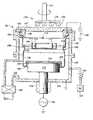
- FIG. 1is schematic top view of one embodiment of an integrated multi-chamber apparatus suitable for depositing a conformal PVD layer on a semiconductor substrate and suitable for annealing the deposited layer;
- FIG. 2is schematic top view of another embodiment of an integrated multi-chamber apparatus suitable for depositing a conformal PVD layer on a semiconductor substrate and suitable for annealing the deposited layer
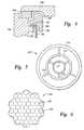
- FIG. 3is a cross-sectional view of one embodiment of a sputtering chamber included within the invention.
- FIG. 4is an expanded view of FIG. 3 including upper area of the shields near the target;
- FIG. 5is a plan view of one embodiment of a ring collimator
- FIG. 6is a partial plan view of one embodiment of a honeycomb collimator
- FIG. 7Ais a cross-sectional view of one embodiment of a pedestal for annealing a substrate
- FIG. 7Bis a cross-sectional view of another embodiment of a pedestal for annealing a substrate.
- FIG. 8is a simplified sectional view of a silicide material used as a contact with a transistor.
- Embodiments of the invention described hereinprovide methods and apparatus for forming a metal silicide layer in a deposition chamber or substrate processing system.
- PVDphysical vapor deposition
- One embodiment described below in reference to a physical vapor deposition (PVD) processis provided to illustrate the invention, and should not be construed or interpreted as limiting the scope of the invention. Aspects of the invention may be used to advantage in other processes, such as chemical vapor deposition, in which an anneal is desired for forming metal silicide layers.
- FIG. 1is schematic top view of one embodiment of an integrated multi-chamber substrate processing system suitable for performing at least one embodiment the metal deposition and annealing processes described herein.
- the deposition and annealing processesmay be performed in a multi-chamber processing system or cluster tool having a PVD chamber disposed thereon.
- One processing platform that may be used to advantageis an EnduraTM processing platform commercially available from Applied Materials, Inc., located in Santa Clara, Calif.
- the processing platform 35typically includes a cluster of process chambers including two transfer chambers 48 , 50 and at least one long throw physical vapor deposition (PVD) chamber 36 , additional processing chambers 38 and 40 , and an annealing chamber 41 .
- the annealing chambers 41 and the PVD chambers 36are disposed in separate transfer chambers, which are operated at different vacuum pressures.
- Chambers 38 and 40may include PVD chambers or chemical vapor deposition (CVD) chambers for depositing other materials as desired by the operator.
- Rapid thermal annealing (RTA) chambersthat can anneal substrates at vacuum pressures may be used for the annealing chamber 41 on transfer chamber 48 or 50 based upon the configuration desired by the operator.
- the processing platform 35may further comprise one or more pre-clean chambers 42 , such as PreClean II chambers available from Applied Materials, for removing contaminants, two degas chambers 44 , and two load lock chambers 46 .
- the processing platform 35typically includes transfer robots 49 , 51 , disposed in transfer chambers 48 , 50 respectfully, and two cooldown or pre-heating chambers 52 separating the transfer chambers 48 , 50 .
- the processing platform 35is automated by programming a microprocessor controller 54 .
- RTA chambers(not shown) may also be disposed on the first transfer chamber 48 of the processing platform 35 to provide post deposition annealing processes prior to substrate removal from the platform 35 .
- a plurality of vacuum pumpsare disposed in fluid communication with each transfer chamber and each of the processing chambers to independently regulate pressures in the respective chambers.
- the pumpsmay establish a vacuum gradient of increasing pressure across the apparatus from the load lock chamber to the processing chambers.
- FIG. 2is a schematic top view of another embodiment of an integrated multi-chamber substrate processing system suitable for performing at least one embodiment the metal deposition and annealing processes described herein.
- two PVD deposition chamberare disposed on the first transfer chamber 48 with two degas chambers 44 , and two load lock chambers 46 .
- One of the PVD deposition chambersmay be substitute with a vacuum annealing chamber or a pre-clean chamber 42 , such as the PreClean II chamber.
- Two annealing chambers 41are disposed on the second transfer chamber 50 .
- the operating pressure of the first transfer chamber 48is generally lower than that for the second transfer chamber 50 since high vacuum PVD processes are performed on the first transfer chamber 48 and high pressure processes, such as atmosphere annealing processes, are performed on the second transfer chamber 50 .
- FIG. 3illustrates one embodiment of a long throw physical vapor deposition chamber.
- suitable long throw PVD chambersare ALPS plusTM and SIPTM PVD processing chambers, both commercially available from Applied Materials, Inc., Santa Clara, Calif.
- the long throw PVD chamber 36contains a sputtering source, such as a target 142 , and a substrate support pedestal 152 for receiving a semiconductor substrate 154 thereon and located within a grounded enclosure wall 150 , which may be a chamber wall as shown or a grounded shield.
- a sputtering sourcesuch as a target 142
- a substrate support pedestal 152for receiving a semiconductor substrate 154 thereon and located within a grounded enclosure wall 150 , which may be a chamber wall as shown or a grounded shield.
- the chamber 36includes a target 142 supported on and sealed by O-rings to a grounded conductive aluminum adapter 144 through a dielectric isolator 146 .
- the target 142may be a bonded composite of a metallic cobalt surface layer and a backing plate of a more workable metal.
- the target 142comprises the material to be deposited on the substrate surface during sputtering.
- the targetmay include, for example, materials including cobalt, titanium, tantalum, tungsten, molybdenum, platinum, nickel, iron, niobium, palladium, and combinations thereof, which are used in forming metal silicide layers.
- targets comprising elemental cobalt, nickel cobalt alloys, or nickel iron alloysmay be used as the target 142 .
- a controllable DC power source 148applies a negative voltage or bias to the target 142 , typically between about between about 0 V and about 2400 V to the target 142 to excite the gas into a plasma state.
- the adapter 144in turn is sealed and grounded to an aluminum chamber sidewall 150 . Ions from the plasma bombard the target 142 to sputter atoms and larger particles onto the substrate 154 disposed below. While, the power supplied is expressed in voltage, power may also be expressed as kilowatts or a power density (W/cm 2 ). The amount of power supplied to the chamber may be varied depending upon the amount of sputtering and the size of the substrate size being processed.
- a pedestal 152supports a substrate 154 to be sputter coated in planar opposition to the principal face of the target 142 .
- the substrate support pedestal 152has a planar substrate receiving surface disposed generally parallel to the sputtering surface of the target 142 .
- the substrate 154is positioned on the substrate support pedestal 152 and plasma is generated in the chamber 36 .
- a long throw distance of at least about 90 mmseparates the target 142 and the substrate.
- the substrate support pedestal 152 and the target 142may be separated by a distance between about 100 mm and about 300 mm for a 200 mm substrate.
- the substrate support pedestal 152 and the target 142may be separated by a distance between about 150 mm and about 400 mm for a 300 mm substrate. Any separation between the substrate and target that is greater than 50% of the substrate diameter is considered a long throw processing chamber.
- a RF power supply 156 in some applicationsis connected to the pedestal electrode 152 in order to induce a negative DC self-bias on the substrate 154 , but in other applications the pedestal 152 is grounded or left electrically floating.
- the D.C. power supply 148 or another power supplymay be used to apply a negative bias, for example, between about 0 V and about 500 V, to the substrate support pedestal 152 .
- the pedestal 152is vertically movable through a bellows 158 connected to a lower chamber wall 160 to allow the substrate 154 to be transferred onto the pedestal 152 through an load lock valve (not shown) in the lower portion of the chamber and thereafter raised to a deposition position.
- Processing working gasis supplied from a gas source 162 through a mass flow controller 164 into the lower part of the chamber.
- a vacuum pumping system 166 connected through a pumping port 168 in the lower chamberis capable of maintaining the chamber at a base pressure of less than 10 ⁇ 6 Torr, but the processing pressure within the chamber is typically maintained at between 0.2 and 2 milliTorr, preferably less than 1 milliTorr, for cobalt sputtering.
- the processing gasincludes non-reactive or inert species such as argon (Ar), xenon (Xe), helium (He), or combinations thereof.
- a rotatable magnetron 170is positioned in back of the target 142 and includes a plurality of horseshoe magnets 172 supported by a base plate 174 connected to a rotation shaft 176 coincident with the central axis of the chamber 140 and the substrate 154 .
- the horseshoe magnets 172are arranged in closed pattern typically having a kidney shape. They produce a magnetic field within the chamber, generally parallel and close to the front face of the target 142 to trap electrons and thereby increase the local plasma density, which in turn increases the sputtering rate.
- the magnets 172are rotated so as to more uniformly sputter the target 142 and coat the substrate 154 .
- the chamber 36 of the inventionincludes a grounded bottom shield 180 having, as is more clearly illustrated in the exploded cross-sectional view of FIG. 4, an upper flange 182 supported on and electrically connected to a ledge 184 of the adapter 144 .
- a dark space shield 186is supported on the flange 182 of the bottom shield 180 , and screws (not shown) recessed in the upper surface of the dark space shield 186 fix it and the flange 182 to the adapter ledge 184 having tapped holes receiving the screws.
- This metallic threaded connectiongrounds the two shields 180 , 186 to the adapter 144 .
- Both shields 180 , 186are typically formed from hard, non-magnetic stainless steel.
- the dark space shield 186has an upper portion that closely fits an annular side recess of the target 142 with a narrow gap 188 between the dark space shield 186 and the target 142 which is sufficiently narrow to prevent the plasma to penetrate, hence protecting the ceramic isolator 146 from being sputter coated with a metal layer, which would electrically short the target 142 .
- the dark space shield 186also includes a downwardly projecting tip 190 , which prevents the interface between the bottom shield 180 and dark space shield 186 from becoming bonded by sputter deposited metal.
- the bottom shield 180extends downwardly in a upper generally tubular portion 194 of a first diameter and a lower generally tubular portion 196 of a smaller second diameter to extend generally along the walls of the adapter 144 and the chamber body 150 to below the top surface of the pedestal 152 . It also has a bowl-shaped bottom including a radially extending bottom portion 198 and an upwardly extending inner portion 100 just outside of the pedestal 152 .
- a cover ring 102rests on the top of the upwardly extending inner portion 100 of the bottom shield 180 when the pedestal 152 is in its lower, loading position but rests on the outer periphery of the pedestal 152 when it is in its upper, deposition position to protect the pedestal 152 from sputter deposition.
- An additional deposition ring(not shown) may be used to shield the periphery of the substrate 154 from deposition.
- the chamber 36may also be adapted to provide a more directional sputtering of material onto a substrate.
- directional sputteringmay be achieved by positioning a collimator 110 positioned between the target 142 and the substrate support pedestal 152 to provide a more uniform and symmetrical flux of deposition material on the substrate 154 .
- a metallic ring collimator 110rests on the ledge portion 106 of the lower shield, thereby grounding the collimator 110 .
- the ring collimator 110includes, as better illustrated in the plan view of FIG. 5, three concentric tubular sections 112 , 114 , 116 linked by cross struts 118 , 120 .
- the outer tubular section 116rests on the ledge portion 106 of the lower shield 180 .
- the use of the lower shield 180 to support the collimator 110simplifies the design and maintenance of the chamber.
- At least the two inner tubular sections 112 , 114are sufficiently high to define high aspect-ratio apertures that partially collimate the sputtered particles.
- the upper surface of the collimator 110acts as a ground plane in opposition to the biased target 142 , particularly keeping plasma electrons away from the substrate 154 .
- FIG. 6Another type of collimator usable with the invention is a honeycomb collimator 124 , partially illustrated in the plan view of FIG. 6 having a mesh structure with hexagonal walls 126 separating hexagonal apertures 128 in a close-packed arrangement.
- An advantage of the honeycomb collimator 124is, if desired, the thickness of the collimator 124 can be varied from the center to the periphery of the collimator, usually in a convex shape, so that the apertures 128 have aspect ratios that are likewise varying across the collimator 124 .
- the collimatormay have one or more convex sides. This allows the sputter flux density to be tailored across the substrate, permitting increased uniformity of deposition. Collimators that may be used in the PVD chamber are described in U.S. Pat. No. 5,650,052, issued Jul. 22, 1997, which is hereby incorporated by reference herein to the extent not inconsistent with aspects of the invention and claims described herein.
- embodiments of the substrate support pedestal 152may be heated by resistive heaters electrically coupled to a power source and may be cooled by a thermal medium passing through fluid conductors connected fluid source, i.e., a liquid heat exchanger.
- a thermal medium passing through fluid conductors connected fluid sourcei.e., a liquid heat exchanger.
- Embodiments of the substrate support pedestal 152are described below, and are provided for illustrative purposes and should not be construed or interpreted as limiting the scope of the invention.
- FIG. 7AOne embodiment of a substrate support pedestal 152 is shown in FIG. 7A.
- the substrate support pedestal 152is suitable for use in a high temperature high vacuum annealing process.
- the substrate support pedestal 152includes a heating portion 210 disposed on a base 240 coupled to a shaft 245 .
- the heating portion 210generally includes heating elements 250 disposed in a thermally conducting material 220 and a substrate support surface 275 .
- the thermally conducting material 220may be any material that has sufficient thermal conductance at operating temperatures for efficient heat transfer between the heating elements 250 and a substrate support surface 275 .
- An example of the conducting materialis steel.
- the substrate support surface 275may include a dielectric material and typically includes a substantially planar receiving surface for a substrate 280 disposed thereon.
- the heating elements 250may be resistive heating elements, such as electrically conducting wires having leads embedded within the conducting material 220 , and are provided to complete an electrical circuit by which electricity is passed through the conducting material 220 .
- An example of a heating element 250includes a discrete heating coil disposed in the thermally conducting material 220 . Electrical wires connect a voltage source (not shown) to the ends of the electrically resistive heating coil to provide energy sufficient to heat the coil.
- the coilmay take any shape that covers the area of the substrate support pedestal 152 . More than one coil may be used to provide additional heating capability, if needed.
- the bodyprovides support for the heating portion and includes fluid channels 290 disposed therein.
- the fluid channels 290are generally coupled to a surface of the heating portion 210 and may provide for either heating or cooling of the substrate support pedestal 152 .
- the combination of heating elements 250 and fluid channels 290generally achieve temperature control of the surface of the substrate support pedestal 152 .
- the fluid channels 290may include a concentric ring or series of rings, or other desired configuration, having fluid inlets and outlets for circulating a liquid from a remotely located source (not shown).
- the fluid channels 290are connected to the fluid source 294 by fluid passage 292 formed in the shaft 245 of substrate support pedestal 152 .
- the heating elements 250can heat the substrate on the substrate support pedestal up to about 900° C. and the fluid channels may cool the substrate to a temperature of about 0° C.
- the combination of heating elements 250 and the fluid channels 290are generally used to control the temperature of a substrate 280 between about 10° C. and about 900° C., subject to properties of materials used in substrate support pedestal 152 and the process parameters used for processing a substrate in the chamber 36 .
- Temperature sensors 260may be attached to or embedded in the substrate support pedestal 152 , such as adjacent the heating portion 210 , to monitor temperature in a conventional manner. For example, measured temperature may be used in a feedback loop to control electric current applied to the resistive heaters from a power supply, such that substrate temperature can be maintained or controlled at a desired temperature or within a desired temperature range.
- a control unit(not shown) may be used to receive a signal from temperature sensor and control the heat power supply or a fluid source in response.
- the power supply and the fluid supply of the heating and cooling componentsare generally located external of the chamber 36 .
- each of the resistive heaterscommunicate via voltage sources by wires disposed through utility passages (not shown) formed in the base 240 and shaft 245 of the substrate support pedestal 152 and are coupled to utility sources, such as power, located externally to the chamber 36 .
- the utility passages, including the fluid passage 294are disposed axially along the base 240 and shaft 245 of the substrate support pedestal 152 .
- a protective, flexible sheath 295is disposed around the shaft 245 and extends from the substrate support pedestal 152 to the chamber wall (not shown) to prevent contamination between the substrate support pedestal 152 and the inside of the chamber.
- the substrate support pedestal 152may further contain gas channels (not shown) fluidly connecting with the substrate receiving surface 275 of the heating portion 210 to a source of backside gas (not shown).
- the fluid channels 270define a backside gas passage control passage of a heat transfer gas or masking gas between the heating portion and the substrate 280 .
- a support pedestal disposed in the chambermay include an electrostatic chuck for supporting a substrate during deposition.
- electrostatic chucksinclude MCATM Electrostatic E-chuck or Pyrolytic Boron Nitride Electrostatic E-Chuck, both available from Applied Materials, Inc., of Santa Clara, Calif.
- FIG. 7Billustrates another embodiment of the substrate support pedestal 152 having an electrostatic chuck 210 mounted to or forming the heating portion of the substrate support pedestal 152 .
- the electrostatic chuck 210includes an electrode 230 and a substrate receiving surface 275 coated with a dielectric material 235 . Electrically conducting wires (not shown) couple the electrodes 230 to a voltage source (not shown).
- a substrate 280may be placed in contact with the dielectric material 235 , and a direct current voltage is placed on the electrode 230 to create the electrostatic attractive force to grip the substrate.
- the electrodes 230are disposed in the thermally conducting material 220 in a spaced relationship with the heating elements 250 disposed therein.
- the heating elements 250are generally disposed in a vertically spaced and parallel manner from the electrodes 230 in the thermally conducting material 220 .
- the electrodesare disposed between the heating elements and the substrate receiving surface 275 though other configurations may be used.
- Fluid channels 290 disposed on a bottom portion of the electrostatic chuck 210may also be used to achieve temperature control of the substrate support pedestal 152 and are connected to the fluid source by fluid passage 292 formed in the substrate support pedestal base 240 .
- Temperature sensors 260are attached to or embedded in the electrostatic chuck 210 to monitor temperature.
- the electrostatic chuck 210may further contain channels 270 formed in the substrate support pedestal 152 fluidly connecting with the substrate receiving surface 275 of the electrostatic chuck 210 to a source of backside gas (not shown).
- the fluid channels 270define a backside gas passage control passage of a heat transfer gas or masking gas between the electrostatic chuck 210 and the substrate 280 .
- the embodiments of the substrate support pedestals 152 described abovemay be used to form a high vacuum anneal chamber.
- the high vacuum anneal chambermay include substrate support pedestals 152 disposed in a PVD chamber, such as the long throw chamber 36 described herein, with a blank target disposed therein or without a target and without bias coupled to either the target or substrate support pedestal.
- a substrateis disposed on the substrate support pedestal, and the substrate is heated, with or without the presence of a backside gas, by the heating elements 250 to the desired processing temperature, processed for sufficient time to anneal the substrate for the desired anneal results, and then removed from the chamber.
- substrate support pedestal 152may be used to anneal the substrate
- commercially available anneal chamberssuch as rapid thermal anneal (RTA) chambers may also be used to anneal the substrate to form the silicide films.
- RTArapid thermal anneal
- the inventioncontemplates utilizing a variety of thermal anneal chamber designs, including hot plate designs and heated lamp designs, to enhance the electroplating results.
- One particular thermal anneal chamber useful for the present inventionis the WxZTM chamber available from Applied materials, Inc., located in Santa Clara, Calif.
- One particular hot plate thermal anneal chamber useful for the present inventionis the RTP XEplus Centura® thermal processing chamber available from Applied Materials, Inc., located in Santa Clara, Calif.
- One particular lamp anneal chamberis the RadianceTM thermal processing chamber available from Applied Materials, Inc., located in Santa Clara, Calif.
- Anneal chambers capable of operating at vacuum pressuresmay be disposed on the PVD transfer chamber 50 , to allow post deposition annealing without breaking vacuum.
- Anneal chamber that are capable of operating at near atmosphere pressuresmay be disposed on the first transfer chamber 48 .
- PVD deposition chambers with cobalt targetsare disposed on the first transfer chamber 48 and the anneal chambers 41 that are capable of operating at near atmosphere pressures may be disposed on the second transfer chamber 50 .
- the deposition and annealing step used in forming a metal silicide layermay be formed in situ, such as in a deposition chamber or in a processing system without breaking vacuum.
- In situis broadly defined herein as performing two or more processes in the same chamber or in the same processing system without breaking vacuum.
- in situ annealingmay be performed in the same processing chamber as the metal deposition.
- in situ annealingmay be performed in a chamber adjacent to the deposition chamber, both of which are coupled to a transfer chamber, and the vacuum on the transfer chamber is not broken during processing.
- in situ annealingmay be performed on the same processing system at separate processing pressures, such as processing a substrate in processing chambers and annealing chambers disposed on the first and second transfer chambers 48 , 50 , respectfully, in system 35 without breaking the vacuum on the system 35 or tranfer of th substrate to another processing system.
- the inventioncontemplates the use of other materials, including titanium, tantalum, tungsten, molybdenum, platinum, nickel, iron, niobium, palladium, and combinations thereof, to form the metal silicide material as described herein.
- a metal layermay be deposited on a silicon substrate disposed in chamber 36 and annealed on the substrate pedestal 152 to form the metal silicide layer without breaking vacuum.
- Metal for forming the metal silicide layeris deposited using the PVD chamber 36 described above.
- the target 142 of material, such as cobalt, to be depositedis disposed in the upper portion of the chamber 36 .
- a substrate 154is provided to the chamber 36 and disposed on the substrate support pedestal 152 .
- the substrate 154includes silicon material disposed thereon and is generally patterned to define features into which metal silicide films will be formed.
- a processing gasis introduced into the chamber 38 at a flow rate of between about 5 sccm and about 30 sccm.
- the chamber pressureis maintained below about 5 milliTorr to promote deposition of conformal PVD metal layers.
- a chamber pressurebetween about 0.2 milliTorr and about 2 milliTorr may be used during deposition. More preferably, a chamber pressure between about 0.2 milliTorr and about 1.0 milliTorr has been observed to be sufficient for sputtering cobalt onto a substrate.
- a plasmais generated by applying a power level to the target 142 between about 0 volts (V) and about 2400 V.
- a power levelis delivered to the target 142 at between about 0 V and about 1000 V to sputter material on a 200 mm substrate.
- a power level between about 0 V and about 500 Vmay be applied to the substrate support pedestal 152 to improve directionality of the sputtered material to the substrate surface.
- the substrateis maintained at a temperature between about 10° C. and about 500° C. during the deposition process.
- An example of a deposition processincludes introducing an inert gas, such as argon, into the chamber at a flow rate between about 5 sccm and about 30 sccm, maintaining a chamber pressure between about 0.2 milliTorr and about 1.0 milliTorr, applying a negative bias of between about 0 volts and about 1000 volts to the target 142 to excite the gas into a plasma state, maintaining the substrate at a temperature between about 10° C. and about 500° C., preferably about 50° C. and about 300° C., and most preferably, between about 50° C. and about 100° C.
- an inert gassuch as argon
- Cobaltmay be deposited on the silicon material at a rate between about 300 ⁇ /min and about 2000 ⁇ /min using this process.
- the cobalt and silicon layeris then annealed in situ at a temperature between about 300° C. and about 900° C. for between about 10 seconds and about 600 seconds to form the metal silicide layer.
- the annealing processmay be performed under an inert gas environment in the deposition chamber by first introducing an inert gas into the chamber at a flow rate between about 0 sccm (Le., no backside gas) and about 15 sccm, maintaining a chamber pressure between of about 2 milliTorr or less, heating the substrate to a temperature between about 300° C. and about 900° C. for between about 5 seconds and about 600 seconds to form the metal silicide layer.
- the metalmay be deposited at substrate temperature of 200° C. or less, and then rapidly annealed on the substrate support pedestal 152 at temperatures of about 400° C. or greater by introducing a backside gas flow.
- An example of a deposition processincludes introducing an inert gas, such as argon, into the chamber at a flow rate between about 5 sccm and about 30 sccm, maintaining a chamber pressure between about 0.2 milliTorr and about 1.0 milliTorr, applying a negative bias of between about 0 volts and about 1000 volts to the target 142 to excite the gas into a plasma state, maintaining the substrate at a temperature of about 200° C., and spacing the target between about 100 mm and about 300 mm from the substrate surface for a 200 mm substrate.
- an inert gassuch as argon
- the substrate temperaturemay be maintained at about 200° C. by heating the substrate in the absence of a backside gas at a heating level that would normally heat the substrate to temperatures of 400° C. or greater. This reduced temperature control is achieved by inefficient heat transfer between the pedestal surface and the backside of the substrate at vacuum pressures. Cobalt may be deposited on the silicon material at a rate between about 300 ⁇ /min and about 2000 ⁇ /min using this process.
- the annealing processcan then be performed in the deposition chamber by ending the plasma and applying a backside gas to the substrate support to enhance heating of the substrate to a temperature between about 400° C. and 600° C. at the same heating levels used for the deposition process.
- the annealing processis performed at a temperature between about 400° C. and about 600° C. for between about 5 seconds and about 300 seconds.
- the substrateis annealed in the deposition chamber at 500° C. for between about 60 seconds and 120 seconds.
- the metal layermay be physical vapor deposited on a silicon substrate in chamber 36 , annealed for a first temperature for a first period of time, transferred to a second chamber, for example chamber 41 , in the system 35 , and annealed at a second temperature for a second period of time to form the metal suicide layer without breaking vacuum.
- the physical vapor deposition of the metalis performed as described above at a temperature of about 200° C. or less, preferably between about 0° C. and about 100° C.
- the first step of the two step in situ annealing process described abovemay be performed under an inert gas environment in the deposition chamber by first introducing an inert gas into the chamber at a flow rate between about 0 sccm and about 15 sccm, maintaining a chamber pressure between about 0 milliTorr and about 2 milliTorr, heating the substrate to a temperature between about 400° C. and about 600° C. for between about 5 seconds and about 300 seconds.
- the substrateis annealed in the deposition chamber at 500° C. for between about 60 seconds and 120 seconds.
- the substrateis then removed from the deposition chamber and transferred to a vacuum anneal chamber disposed on the same transfer chamber, such as transfer chamber 48 described above in FIG. 2.
- the high vacuum anneal chambermay include a PVD chamber having a blank target and substrate support pedestal 152 described above or a commercial high vacuum anneal pedestal, such as the High Temperature High Uniformity, HTHUTM substrate support commercially available from Applied Materials Inc., of Santa Clara Calif.
- the second annealing stepmay then be performed by maintaining a chamber pressure between about 0 milliTorr and about 2 milliTorr and heating the substrate to a temperature between about 600° C. and about 900° C. for a period of time between about 5 seconds and about 300 seconds to form the metal silicide layer.
- the substrateis annealed in the anneal chamber at 800° C. for between about 60 seconds and 120 seconds.
- the metal layeris deposited according to the process described herein at about 200° C. or less, preferably between about 0° C. and about 100° C., in the deposition chamber.
- the substrateis then annealed in the deposition chamber according to the anneal process described above.
- the substratemay then be transferred to a RTA chamber disposed on transfer chamber 50 in FIG. 2 for a second anneal process.
- Annealing in an RTA anneal chambermay be performed by introducing a process gas including nitrogen (N 2 ), argon (Ar), helium (He), and combinations thereof, with less than about 4% hydrogen (H 2 ), at a process gas flow rate greater than 20 liters/min to control the oxygen content to less than 100 ppm, maintaining a chamber pressure of about ambient, and heating the substrate to a temperature between about 600° C. and about 900° C. for between about 5 seconds and about 300 seconds to form the metal silicide layer.
- the substrateis annealed in the RTA anneal chamber at 800° C. for about 30 seconds.
- the metal layermay be deposited on a silicon substrate in chamber 36 , transferred to a first anneal chamber, such as a vacuum anneal chamber disposed on the same transfer chamber 48 on the system 35 , annealed for a first temperature for a first period of time, transferred to a second anneal chamber, for example chamber 41 , in the system 35 , and annealed at a second temperature for a second period of time to form the metal suicide layer without breaking vacuum.
- a first anneal chambersuch as a vacuum anneal chamber disposed on the same transfer chamber 48 on the system 35
- annealed for a first temperature for a first period of timetransferred to a second anneal chamber, for example chamber 41 , in the system 35 , and annealed at a second temperature for a second period of time to form the metal suicide layer without breaking vacuum.
- the metal depositionis performed in the deposition chamber according to the process described above at a substrate temperature of about 200° C. or less, preferably between about 0° C. and about 100° C.
- the first step of this embodiment of the annealing processmay be performed in situ in a first high vacuum anneal chamber disposed on a processing system by introducing an inert gas into the anneal chamber at a flow rate between about 0 sccm and about 15 sccm, maintaining a chamber pressure between about 0 milliTorr and about 2 milliTorr, heating the substrate to a temperature between about 400° C. and about 600° C. for between about 5 seconds and about 300 seconds.
- the substrateis annealed in the deposition chamber at 500° C. for between about 60 seconds and 120 seconds.
- the first annealing stepis believed to form an oxygen resistant film such as CoSi.
- the substratemay be annealed in situ by transfer to a second high vacuum annealing chamber in the processing system.
- the second annealing stepmay then be performed by maintaining a chamber pressure of about 2 milliTorr or less and heating the substrate to a temperature between about 600° C. and about 900° C. for a period of time between about 5 seconds and about 300 seconds to form the metal silicide layer.
- the substrateis annealed in the anneal chamber at 800° C. for between about 60 seconds and 120 seconds.
- the substratemay be transferred to a second annealing chamber located outside the transfer chamber or processing system, such as an atmosphere pressure RTA chamber.
- Annealing in an RTA anneal chambermay be performed by introducing a process gas including nitrogen (N 2 ), argon (Ar), helium (He), and combinations thereof, with less than about 4% hydrogen (H 2 ), at a process gas flow rate greater than 20 liters/min to control the oxygen content to less than 100 ppm, maintaining a chamber pressure of about ambient, and heating the substrate to a temperature between about 400° C. and about 900° C. for between about 5 seconds and about 300 seconds to form the metal suicide layer.
- the substrateis annealed in the RTA anneal chamber at 800° C. for about 30 seconds.
- the metalmay be deposited at a high deposition temperature.
- An example of a deposition processincludes introducing an inert gas, such as argon, into the chamber at a flow rate between about 5 sccm and about 30 sccm, maintaining a chamber pressure between about 0.2 milliTorr and about 1.0 milliTorr, applying a negative bias of between about 0 volts and about 1000 volts to the target 142 to excite the gas into a plasma state, maintaining the substrate at about an annealing temperature, Le., between about 400° C. and about 600° C. by applying a backside gas, and spacing the target between about 100 mm and about 300 mm from the substrate surface for a 200 mm substrate.
- the temperaturemay be maintained at about 200° C. by heating the substrate in the absence of a backside gas.
- Cobaltmay be deposited on the silicon material at a rate between about 300 ⁇ /min and about 2000 ⁇ /min using this process.
- the annealing processcan then be performed in the deposition chamber by ending the plasma and heating of the substrate to a temperature between about 400° C. and 600° C. at the same heating levels used for the deposition process.
- the annealing processis performed at a temperature between about 400° C. and about 600° C. for between about 5 seconds and about 300 seconds.
- the substrateis annealed in the deposition chamber at 500° C. for between about 60 seconds and 120 seconds.
- the second annealing stepmay then be formed in an annealing chamber without breaking vacuum or in an annealing chamber located on a separate transfer chamber or processing system.
- the second annealing stepincludes heating the substrate to a temperature between about 600° C. and about 900° C. for a period of time between about 5 seconds and about 300 seconds to form the metal silicide layer.
- the substrateis annealed at 800° C. for between about 60 seconds and 120 seconds.
- the metal silicide materialincluding suicides of cobalt, titanium, tantalum, tungsten, molybdenum, platinum, nickel, iron, niobium, palladium, and combinations thereof, may be used in the formation of a MOS device shown in FIG. 8.
- N+ source and drain regions 402 and 404are formed in a P type silicon substrate 400 adjacent field oxide portions 406 .
- a gate oxide layer 408 and a polysilicon gate electrode 410are formed over silicon substrate 400 in between source and drain regions 402 and 404 with oxide spacers 412 formed on the sidewalls of polysilicon gate electrode 410 .
- a cobalt layeris deposited over the MOS structure, and in particular over the exposed silicon surfaces of source and drain regions 402 and 404 and the exposed top surface of polysilicon gate electrode 410 by the process described herein.
- the cobalt materialis deposited to a thickness of at about 1000 ⁇ or less to provide a sufficient amount of cobalt for the subsequent reaction with the underlying silicon at 402 and 404 .
- Cobaltmay be deposited to a thickness between about 50 ⁇ and about 500 ⁇ on the silicon material.
- the cobalt layeris then annealed in situ as described herein to form cobalt silicide.
Landscapes
- Engineering & Computer Science (AREA)
- Chemical & Material Sciences (AREA)
- Computer Hardware Design (AREA)
- General Physics & Mathematics (AREA)
- Power Engineering (AREA)
- Microelectronics & Electronic Packaging (AREA)
- Manufacturing & Machinery (AREA)
- Physics & Mathematics (AREA)
- Condensed Matter Physics & Semiconductors (AREA)
- Chemical Kinetics & Catalysis (AREA)
- Metallurgy (AREA)
- Organic Chemistry (AREA)
- General Chemical & Material Sciences (AREA)
- Mechanical Engineering (AREA)
- Materials Engineering (AREA)
- Electrodes Of Semiconductors (AREA)
- Physical Vapour Deposition (AREA)
- Chemical Vapour Deposition (AREA)
Abstract
Description
- 1. Field of the Invention[0001]
- The present invention relates to the fabrication of semiconductor devices and to the deposition and annealing of materials on a semiconductor substrate.[0002]
- 2. Description of the Related Art[0003]
- Recent improvements in circuitry of ultra-large scale integration (ULSI) on semiconductor substrates indicate that future generations of semiconductor devices will require sub-quarter micron multi-level metallization. The multilevel interconnects that lie at the heart of this technology require planarization of interconnect features formed in high aspect ratio apertures, including contacts, vias, lines and other features. Reliable formation of these interconnect features is very important to the success of ULSI and to the continued effort to increase circuit density and quality on individual substrates and die.[0004]
- ULSI circuits include metal oxide semiconductor (MOS) devices, such as complementary metal oxide semiconductor (CMOS) field effect transistors (FETs). The transistors can include semiconductor gates disposed between source and drain regions. In the formation of integrated circuit structures, and particularly in the formation of MOS devices using polysilicon gate electrodes, it has become the practice to provide a metal silicide layer over the polysilicon gate electrode, and over the source and drain regions of the silicon substrate, to facilitate lower resistance and improve device performance by electrically connecting the source and drain regions to metal interconnects.[0005]
- One important processing technique currently used in CMOS processing technology is the Self-Aligned Silicidation (salicide) of refractory metals such as titanium and cobalt. In a salicide process using cobalt (Co), for example, the source and drain and polysilicon gate resistances are reduced by forming a high conductivity overlayer and the contact resistance is reduced by increasing the effective contact area of the source and drain with subsequently formed metal interconnects. Salicide processing technology seeks to exploit the principle that a refractory metal such as cobalt deposited on a patterned silicon substrate will selectively react with exposed silicon under specific processing conditions, and will not react with silicon oxide material.[0006]
- For example, a layer of cobalt is sputtered onto silicon, typically patterned on a substrate surface, and then subjected to a thermal annealing process to form cobalt silicide (CoSi[0007]2). Unreacted cobalt, such as cobalt deposited outside the patterned silicon or on a protective layer of silicon oxide, can thereafter be selectively etched away. The selective reaction of cobalt silicide will result in maskless, self-aligned formation of a low-resistivity refractory metal silicide in source, drain, and polysilicon gate regions formed on the substrate surface and in interconnecting conductors of the semiconductor device. After the etch process, further processing of the substrate may occur, such as additional thermal annealing, which may be used to further reduce the sheet resistance of the silicide material.
- However, it has been difficult in integrating cobalt silicide processes into conventional manufacturing equipment. Current processing systems performing cobalt silicide processes require transfer of the substrate between separate chambers for the deposition and annealing process steps. Transfer between chambers may expose the substrate to contamination and potential oxidation of silicon or cobalt deposited on the substrate surface[0008]
- Oxide formation on the surface of the substrate can result in increasing the resistance of silicide layers as well reducing the reliability of the overall circuit. For example, oxidation of the deposited cobalt material may result in cobalt agglomeration and irregular growth of the silicide layer. The agglomeration and irregular growth of the cobalt layer may result in device malformation, such as source and drain electrodes having different thicknesses and surface areas. Additionally, excess cobalt silicide growth on substrate surface may form conductive paths between devices, which may result in short circuits and device failure.[0009]
- One solution to limiting cobalt and silicon contamination is to sputter a capping film of titanium or titanium nitride on the cobalt and silicon film prior to transferring the substrate between chambers. The capping film is then removed after annealing the substrate and prior to further processing of the substrate. However, the addition of titanium nitride deposition and removal processes increase the number of processing steps required for silicide formation, thereby reducing process efficiency, increasing processing complexity, and reducing substrate through-put.[0010]
- Therefore, there is a need for a method and apparatus for forming suicide materials on a substrate while reducing processing complexity and improving processing efficiency and throughput.[0011]
- Embodiments of the invention described herein generally provide methods and apparatus for forming a metal suicide layer using a deposition and annealing process. In one aspect, a system is provided for processing a substrate including a load lock chamber, an intermediate substrate transfer region connected to the load lock chamber, the intermediate substrate transfer region comprising a first substrate transfer chamber and a second substrate transfer chamber, wherein the first substrate transfer chamber is coupled to the load lock chamber and the second substrate transfer chamber is coupled to the first substrate transfer chamber, a physical vapor deposition (PVD) processing chamber disposed on the first substrate transfer chamber and an annealing chamber disposed on the second substrate transfer chamber.[0012]
- In another aspect, a method is provided for forming a silicide layer on a substrate including positioning a substrate having silicon material disposed thereon on a substrate support disposed in a deposition chamber having a metal target disposed therein, applying a current to the substrate support to heat the substrate to a first temperature, introducing an inert gas into the deposition chamber, generating a plasma by applying a bias between a metal target and the substrate support in the inert gas environment to sputter material from the metal target, depositing the sputtered material on at least the silicon material, providing a backside gas between the substrate pedestal and the substrate, and annealing the substrate in situ at a second temperature greater than the first temperature to form a metal silicide layer.[0013]
- In another aspect, a method is provided for processing a substrate including introducing a substrate having silicon material disposed thereon into a load lock, transferring the substrate to a first transfer chamber having a physical vapor deposition processing chamber disposed thereon, the first transfer chamber is connected to the loadlock and the depositing chamber has a metal target and heating pedestal disposed therein, positioning the substrate into the physical vapor deposition chamber, depositing a metal layer on the silicon material, annealing the substrate prior to transferring the substrate to a second transfer chamber having an annealing chamber disposed thereon, wherein the second transfer chamber is connected to the first transfer chamber, and annealing the substrate in the annealing chamber to form a metal silicide layer.[0014]
- So that the manner in which the above recited aspects of the invention are attained and can be understood in detail, a more particular description of the invention, briefly summarized above, may be had by reference to the embodiments thereof which are illustrated in the appended drawings.[0015]
- It is to be noted, however, that the appended drawings illustrate only typical embodiments of this invention and are therefore not to be considered limiting of its scope, for the invention may admit to other equally effective embodiments.[0016]
- FIG. 1 is schematic top view of one embodiment of an integrated multi-chamber apparatus suitable for depositing a conformal PVD layer on a semiconductor substrate and suitable for annealing the deposited layer;[0017]
- FIG. 2 is schematic top view of another embodiment of an integrated multi-chamber apparatus suitable for depositing a conformal PVD layer on a semiconductor substrate and suitable for annealing the deposited layer[0018]
- FIG. 3 is a cross-sectional view of one embodiment of a sputtering chamber included within the invention;[0019]
- FIG. 4 is an expanded view of FIG. 3 including upper area of the shields near the target;[0020]
- FIG. 5 is a plan view of one embodiment of a ring collimator;[0021]
- FIG. 6 is a partial plan view of one embodiment of a honeycomb collimator;[0022]
- FIG. 7A is a cross-sectional view of one embodiment of a pedestal for annealing a substrate;[0023]
- FIG. 7B is a cross-sectional view of another embodiment of a pedestal for annealing a substrate; and[0024]
- FIG. 8 is a simplified sectional view of a silicide material used as a contact with a transistor.[0025]
- Embodiments of the invention described herein provide methods and apparatus for forming a metal silicide layer in a deposition chamber or substrate processing system. One embodiment described below in reference to a physical vapor deposition (PVD) process is provided to illustrate the invention, and should not be construed or interpreted as limiting the scope of the invention. Aspects of the invention may be used to advantage in other processes, such as chemical vapor deposition, in which an anneal is desired for forming metal silicide layers.[0026]
- FIG. 1 is schematic top view of one embodiment of an integrated multi-chamber substrate processing system suitable for performing at least one embodiment the metal deposition and annealing processes described herein. The deposition and annealing processes may be performed in a multi-chamber processing system or cluster tool having a PVD chamber disposed thereon. One processing platform that may be used to advantage is an Endura™ processing platform commercially available from Applied Materials, Inc., located in Santa Clara, Calif.[0027]
- The[0028]
processing platform 35 typically includes a cluster of process chambers including twotransfer chambers chamber 36,additional processing chambers annealing chamber 41. Generally, theannealing chambers 41 and thePVD chambers 36 are disposed in separate transfer chambers, which are operated at different vacuum pressures.Chambers chamber 41 ontransfer chamber - The[0029]
processing platform 35 may further comprise one or more pre-cleanchambers 42, such as PreClean II chambers available from Applied Materials, for removing contaminants, twodegas chambers 44, and twoload lock chambers 46. Theprocessing platform 35 typically includestransfer robots transfer chambers chambers 52 separating thetransfer chambers processing platform 35 is automated by programming amicroprocessor controller 54. RTA chambers (not shown) may also be disposed on thefirst transfer chamber 48 of theprocessing platform 35 to provide post deposition annealing processes prior to substrate removal from theplatform 35. While not shown, a plurality of vacuum pumps are disposed in fluid communication with each transfer chamber and each of the processing chambers to independently regulate pressures in the respective chambers. The pumps may establish a vacuum gradient of increasing pressure across the apparatus from the load lock chamber to the processing chambers. - FIG. 2 is a schematic top view of another embodiment of an integrated multi-chamber substrate processing system suitable for performing at least one embodiment the metal deposition and annealing processes described herein. In this embodiment, two PVD deposition chamber are disposed on the[0030]
first transfer chamber 48 with twodegas chambers 44, and twoload lock chambers 46. One of the PVD deposition chambers may be substitute with a vacuum annealing chamber or apre-clean chamber 42, such as the PreClean II chamber. Two annealingchambers 41, are disposed on thesecond transfer chamber 50. The operating pressure of thefirst transfer chamber 48 is generally lower than that for thesecond transfer chamber 50 since high vacuum PVD processes are performed on thefirst transfer chamber 48 and high pressure processes, such as atmosphere annealing processes, are performed on thesecond transfer chamber 50. - FIG. 3 illustrates one embodiment of a long throw physical vapor deposition chamber. Example of suitable long throw PVD chambers are ALPS plus™ and SIP™ PVD processing chambers, both commercially available from Applied Materials, Inc., Santa Clara, Calif.[0031]
- Generally, the long[0032]
throw PVD chamber 36 contains a sputtering source, such as atarget 142, and asubstrate support pedestal 152 for receiving asemiconductor substrate 154 thereon and located within a groundedenclosure wall 150, which may be a chamber wall as shown or a grounded shield. - The[0033]
chamber 36 includes atarget 142 supported on and sealed by O-rings to a groundedconductive aluminum adapter 144 through adielectric isolator 146. Thetarget 142 may be a bonded composite of a metallic cobalt surface layer and a backing plate of a more workable metal. Thetarget 142 comprises the material to be deposited on the substrate surface during sputtering. The target may include, for example, materials including cobalt, titanium, tantalum, tungsten, molybdenum, platinum, nickel, iron, niobium, palladium, and combinations thereof, which are used in forming metal silicide layers. For example, targets comprising elemental cobalt, nickel cobalt alloys, or nickel iron alloys may be used as thetarget 142. - A controllable[0034]
DC power source 148 applies a negative voltage or bias to thetarget 142, typically between about between about 0 V and about 2400 V to thetarget 142 to excite the gas into a plasma state. Theadapter 144 in turn is sealed and grounded to analuminum chamber sidewall 150. Ions from the plasma bombard thetarget 142 to sputter atoms and larger particles onto thesubstrate 154 disposed below. While, the power supplied is expressed in voltage, power may also be expressed as kilowatts or a power density (W/cm2). The amount of power supplied to the chamber may be varied depending upon the amount of sputtering and the size of the substrate size being processed. - A[0035]
pedestal 152 supports asubstrate 154 to be sputter coated in planar opposition to the principal face of thetarget 142. Thesubstrate support pedestal 152 has a planar substrate receiving surface disposed generally parallel to the sputtering surface of thetarget 142. In operation, thesubstrate 154 is positioned on thesubstrate support pedestal 152 and plasma is generated in thechamber 36. A long throw distance of at least about90 mm separates thetarget 142 and the substrate. Thesubstrate support pedestal 152 and thetarget 142 may be separated by a distance between about 100 mm and about 300 mm for a 200 mm substrate. Thesubstrate support pedestal 152 and thetarget 142 may be separated by a distance between about 150 mm and about 400 mm for a 300 mm substrate. Any separation between the substrate and target that is greater than 50% of the substrate diameter is considered a long throw processing chamber. - A[0036]
RF power supply 156 in some applications is connected to thepedestal electrode 152 in order to induce a negative DC self-bias on thesubstrate 154, but in other applications thepedestal 152 is grounded or left electrically floating. TheD.C. power supply 148 or another power supply may be used to apply a negative bias, for example, between about 0 V and about 500 V, to thesubstrate support pedestal 152. Thepedestal 152 is vertically movable through abellows 158 connected to alower chamber wall 160 to allow thesubstrate 154 to be transferred onto thepedestal 152 through an load lock valve (not shown) in the lower portion of the chamber and thereafter raised to a deposition position. - Processing working gas is supplied from a[0037]
gas source 162 through amass flow controller 164 into the lower part of the chamber. Avacuum pumping system 166 connected through a pumpingport 168 in the lower chamber is capable of maintaining the chamber at a base pressure of less than 10−6Torr, but the processing pressure within the chamber is typically maintained at between 0.2 and 2 milliTorr, preferably less than 1 milliTorr, for cobalt sputtering. The processing gas includes non-reactive or inert species such as argon (Ar), xenon (Xe), helium (He), or combinations thereof. - A[0038]
rotatable magnetron 170 is positioned in back of thetarget 142 and includes a plurality ofhorseshoe magnets 172 supported by abase plate 174 connected to arotation shaft 176 coincident with the central axis of the chamber140 and thesubstrate 154. Thehorseshoe magnets 172 are arranged in closed pattern typically having a kidney shape. They produce a magnetic field within the chamber, generally parallel and close to the front face of thetarget 142 to trap electrons and thereby increase the local plasma density, which in turn increases the sputtering rate. Themagnets 172 are rotated so as to more uniformly sputter thetarget 142 and coat thesubstrate 154. - The[0039]
chamber 36 of the invention includes a groundedbottom shield 180 having, as is more clearly illustrated in the exploded cross-sectional view of FIG. 4, anupper flange 182 supported on and electrically connected to aledge 184 of theadapter 144. Adark space shield 186 is supported on theflange 182 of thebottom shield 180, and screws (not shown) recessed in the upper surface of thedark space shield 186 fix it and theflange 182 to theadapter ledge 184 having tapped holes receiving the screws. This metallic threaded connection grounds the twoshields adapter 144. Both shields180,186 are typically formed from hard, non-magnetic stainless steel. Thedark space shield 186 has an upper portion that closely fits an annular side recess of thetarget 142 with anarrow gap 188 between thedark space shield 186 and thetarget 142 which is sufficiently narrow to prevent the plasma to penetrate, hence protecting theceramic isolator 146 from being sputter coated with a metal layer, which would electrically short thetarget 142. Thedark space shield 186 also includes a downwardly projectingtip 190, which prevents the interface between thebottom shield 180 anddark space shield 186 from becoming bonded by sputter deposited metal. - Returning to the overall view of FIG. 3, the[0040]
bottom shield 180 extends downwardly in a upper generallytubular portion 194 of a first diameter and a lower generallytubular portion 196 of a smaller second diameter to extend generally along the walls of theadapter 144 and thechamber body 150 to below the top surface of thepedestal 152. It also has a bowl-shaped bottom including a radially extendingbottom portion 198 and an upwardly extendinginner portion 100 just outside of thepedestal 152. Acover ring 102 rests on the top of the upwardly extendinginner portion 100 of thebottom shield 180 when thepedestal 152 is in its lower, loading position but rests on the outer periphery of thepedestal 152 when it is in its upper, deposition position to protect thepedestal 152 from sputter deposition. An additional deposition ring (not shown) may be used to shield the periphery of thesubstrate 154 from deposition. - The[0041]
chamber 36 may also be adapted to provide a more directional sputtering of material onto a substrate. In one aspect, directional sputtering may be achieved by positioning acollimator 110 positioned between thetarget 142 and thesubstrate support pedestal 152 to provide a more uniform and symmetrical flux of deposition material on thesubstrate 154. - A[0042]
metallic ring collimator 110 rests on theledge portion 106 of the lower shield, thereby grounding thecollimator 110. Thering collimator 110 includes, as better illustrated in the plan view of FIG. 5, three concentrictubular sections tubular section 116 rests on theledge portion 106 of thelower shield 180. The use of thelower shield 180 to support thecollimator 110 simplifies the design and maintenance of the chamber. At least the two innertubular sections collimator 110 acts as a ground plane in opposition to thebiased target 142, particularly keeping plasma electrons away from thesubstrate 154. - Another type of collimator usable with the invention is a[0043]
honeycomb collimator 124, partially illustrated in the plan view of FIG. 6 having a mesh structure withhexagonal walls 126 separatinghexagonal apertures 128 in a close-packed arrangement. An advantage of thehoneycomb collimator 124 is, if desired, the thickness of thecollimator 124 can be varied from the center to the periphery of the collimator, usually in a convex shape, so that theapertures 128 have aspect ratios that are likewise varying across thecollimator 124. The collimator may have one or more convex sides. This allows the sputter flux density to be tailored across the substrate, permitting increased uniformity of deposition. Collimators that may be used in the PVD chamber are described in U.S. Pat. No. 5,650,052, issued Jul. 22, 1997, which is hereby incorporated by reference herein to the extent not inconsistent with aspects of the invention and claims described herein. - Referring to FIGS. 7A and 7B, embodiments of the[0044]
substrate support pedestal 152 may be heated by resistive heaters electrically coupled to a power source and may be cooled by a thermal medium passing through fluid conductors connected fluid source, i.e., a liquid heat exchanger. Embodiments of thesubstrate support pedestal 152 are described below, and are provided for illustrative purposes and should not be construed or interpreted as limiting the scope of the invention. - One embodiment of a[0045]
substrate support pedestal 152 is shown in FIG. 7A. Thesubstrate support pedestal 152 is suitable for use in a high temperature high vacuum annealing process. Generally, thesubstrate support pedestal 152 includes aheating portion 210 disposed on a base240 coupled to ashaft 245. - The[0046]
heating portion 210 generally includesheating elements 250 disposed in a thermally conductingmaterial 220 and asubstrate support surface 275. The thermally conductingmaterial 220 may be any material that has sufficient thermal conductance at operating temperatures for efficient heat transfer between theheating elements 250 and asubstrate support surface 275. An example of the conducting material is steel. Thesubstrate support surface 275 may include a dielectric material and typically includes a substantially planar receiving surface for asubstrate 280 disposed thereon. - The[0047]
heating elements 250 may be resistive heating elements, such as electrically conducting wires having leads embedded within the conductingmaterial 220, and are provided to complete an electrical circuit by which electricity is passed through the conductingmaterial 220. An example of aheating element 250 includes a discrete heating coil disposed in the thermally conductingmaterial 220. Electrical wires connect a voltage source (not shown) to the ends of the electrically resistive heating coil to provide energy sufficient to heat the coil. The coil may take any shape that covers the area of thesubstrate support pedestal 152. More than one coil may be used to provide additional heating capability, if needed. - The body provides support for the heating portion and includes[0048]
fluid channels 290 disposed therein. Thefluid channels 290 are generally coupled to a surface of theheating portion 210 and may provide for either heating or cooling of thesubstrate support pedestal 152. The combination ofheating elements 250 andfluid channels 290 generally achieve temperature control of the surface of thesubstrate support pedestal 152. - The[0049]
fluid channels 290 may include a concentric ring or series of rings, or other desired configuration, having fluid inlets and outlets for circulating a liquid from a remotely located source (not shown). Thefluid channels 290 are connected to thefluid source 294 byfluid passage 292 formed in theshaft 245 ofsubstrate support pedestal 152. - The[0050]
heating elements 250 can heat the substrate on the substrate support pedestal up to about 900° C. and the fluid channels may cool the substrate to a temperature of about 0° C. The combination ofheating elements 250 and thefluid channels 290 are generally used to control the temperature of asubstrate 280 between about 10° C. and about 900° C., subject to properties of materials used insubstrate support pedestal 152 and the process parameters used for processing a substrate in thechamber 36. - [0051]
Temperature sensors 260, such as a thermocouple, may be attached to or embedded in thesubstrate support pedestal 152, such as adjacent theheating portion 210, to monitor temperature in a conventional manner. For example, measured temperature may be used in a feedback loop to control electric current applied to the resistive heaters from a power supply, such that substrate temperature can be maintained or controlled at a desired temperature or within a desired temperature range. A control unit (not shown) may be used to receive a signal from temperature sensor and control the heat power supply or a fluid source in response. - The power supply and the fluid supply of the heating and cooling components are generally located external of the[0052]
chamber 36. For example, each of the resistive heaters communicate via voltage sources by wires disposed through utility passages (not shown) formed in thebase 240 andshaft 245 of thesubstrate support pedestal 152 and are coupled to utility sources, such as power, located externally to thechamber 36. The utility passages, including thefluid passage 294, are disposed axially along thebase 240 andshaft 245 of thesubstrate support pedestal 152. A protective,flexible sheath 295 is disposed around theshaft 245 and extends from thesubstrate support pedestal 152 to the chamber wall (not shown) to prevent contamination between thesubstrate support pedestal 152 and the inside of the chamber. - The[0053]
substrate support pedestal 152 may further contain gas channels (not shown) fluidly connecting with thesubstrate receiving surface 275 of theheating portion 210 to a source of backside gas (not shown). The fluid channels270 define a backside gas passage control passage of a heat transfer gas or masking gas between the heating portion and thesubstrate 280. - A support pedestal disposed in the chamber may include an electrostatic chuck for supporting a substrate during deposition. Examples of suitable electrostatic chucks that may be used for the support pedestal include MCA™ Electrostatic E-chuck or Pyrolytic Boron Nitride Electrostatic E-Chuck, both available from Applied Materials, Inc., of Santa Clara, Calif.[0054]
- FIG. 7B illustrates another embodiment of the[0055]
substrate support pedestal 152 having anelectrostatic chuck 210 mounted to or forming the heating portion of thesubstrate support pedestal 152. Theelectrostatic chuck 210 includes anelectrode 230 and asubstrate receiving surface 275 coated with adielectric material 235. Electrically conducting wires (not shown) couple theelectrodes 230 to a voltage source (not shown). Asubstrate 280 may be placed in contact with thedielectric material 235, and a direct current voltage is placed on theelectrode 230 to create the electrostatic attractive force to grip the substrate. - Generally, the[0056]
electrodes 230 are disposed in the thermally conductingmaterial 220 in a spaced relationship with theheating elements 250 disposed therein. Theheating elements 250 are generally disposed in a vertically spaced and parallel manner from theelectrodes 230 in the thermally conductingmaterial 220. Typically, the electrodes are disposed between the heating elements and thesubstrate receiving surface 275 though other configurations may be used.Fluid channels 290 disposed on a bottom portion of theelectrostatic chuck 210 may also be used to achieve temperature control of thesubstrate support pedestal 152 and are connected to the fluid source byfluid passage 292 formed in the substratesupport pedestal base 240.Temperature sensors 260 are attached to or embedded in theelectrostatic chuck 210 to monitor temperature. - The[0057]
electrostatic chuck 210 may further contain channels270 formed in thesubstrate support pedestal 152 fluidly connecting with thesubstrate receiving surface 275 of theelectrostatic chuck 210 to a source of backside gas (not shown). The fluid channels270 define a backside gas passage control passage of a heat transfer gas or masking gas between theelectrostatic chuck 210 and thesubstrate 280. - The embodiments of the substrate support pedestals[0058]152 described above may be used to form a high vacuum anneal chamber. The high vacuum anneal chamber may include substrate support pedestals152 disposed in a PVD chamber, such as the
long throw chamber 36 described herein, with a blank target disposed therein or without a target and without bias coupled to either the target or substrate support pedestal. In operation, a substrate is disposed on the substrate support pedestal, and the substrate is heated, with or without the presence of a backside gas, by theheating elements 250 to the desired processing temperature, processed for sufficient time to anneal the substrate for the desired anneal results, and then removed from the chamber. - While the embodiments of[0059]
substrate support pedestal 152 described herein may be used to anneal the substrate, commercially available anneal chambers, such as rapid thermal anneal (RTA) chambers may also be used to anneal the substrate to form the silicide films. The invention contemplates utilizing a variety of thermal anneal chamber designs, including hot plate designs and heated lamp designs, to enhance the electroplating results. One particular thermal anneal chamber useful for the present invention is the WxZ™ chamber available from Applied materials, Inc., located in Santa Clara, Calif. One particular hot plate thermal anneal chamber useful for the present invention is the RTP XEplus Centura® thermal processing chamber available from Applied Materials, Inc., located in Santa Clara, Calif. One particular lamp anneal chamber is the Radiance™ thermal processing chamber available from Applied Materials, Inc., located in Santa Clara, Calif. - Anneal chambers capable of operating at vacuum pressures may be disposed on the[0060]
PVD transfer chamber 50, to allow post deposition annealing without breaking vacuum. Anneal chamber that are capable of operating at near atmosphere pressures may be disposed on thefirst transfer chamber 48. In the embodiment shown in FIG. 3, PVD deposition chambers with cobalt targets are disposed on thefirst transfer chamber 48 and theanneal chambers 41 that are capable of operating at near atmosphere pressures may be disposed on thesecond transfer chamber 50. - Metal Silicide Process[0061]
- The deposition and annealing step used in forming a metal silicide layer may be formed in situ, such as in a deposition chamber or in a processing system without breaking vacuum. In situ is broadly defined herein as performing two or more processes in the same chamber or in the same processing system without breaking vacuum. For example, in situ annealing may be performed in the same processing chamber as the metal deposition.[0062]
- In another example, in situ annealing may performed in a chamber adjacent to the deposition chamber, both of which are coupled to a transfer chamber, and the vacuum on the transfer chamber is not broken during processing. In a further example, in situ annealing may be performed on the same processing system at separate processing pressures, such as processing a substrate in processing chambers and annealing chambers disposed on the first and[0063]
second transfer chambers system 35 without breaking the vacuum on thesystem 35 or tranfer of th substrate to another processing system. - While the following material describes the deposition of a cobalt film, the invention contemplates the use of other materials, including titanium, tantalum, tungsten, molybdenum, platinum, nickel, iron, niobium, palladium, and combinations thereof, to form the metal silicide material as described herein.[0064]
- Metal Deposition[0065]
- In one embodiment, a metal layer may be deposited on a silicon substrate disposed in[0066]
chamber 36 and annealed on thesubstrate pedestal 152 to form the metal silicide layer without breaking vacuum. Metal for forming the metal silicide layer is deposited using thePVD chamber 36 described above. Thetarget 142 of material, such as cobalt, to be deposited is disposed in the upper portion of thechamber 36. Asubstrate 154 is provided to thechamber 36 and disposed on thesubstrate support pedestal 152. Thesubstrate 154 includes silicon material disposed thereon and is generally patterned to define features into which metal silicide films will be formed. - A processing gas is introduced into the[0067]
chamber 38 at a flow rate of between about 5 sccm and about 30 sccm. The chamber pressure is maintained below about 5 milliTorr to promote deposition of conformal PVD metal layers. Preferably, a chamber pressure between about 0.2 milliTorr and about 2 milliTorr may be used during deposition. More preferably, a chamber pressure between about 0.2 milliTorr and about 1.0 milliTorr has been observed to be sufficient for sputtering cobalt onto a substrate. - A plasma is generated by applying a power level to the[0068]
target 142 between about 0 volts (V) and about 2400 V. For example, a power level is delivered to thetarget 142 at between about 0 V and about 1000 V to sputter material on a 200 mm substrate. A power level between about 0 V and about 500 V may be applied to thesubstrate support pedestal 152 to improve directionality of the sputtered material to the substrate surface. The substrate is maintained at a temperature between about 10° C. and about 500° C. during the deposition process. - An example of a deposition process includes introducing an inert gas, such as argon, into the chamber at a flow rate between about 5 sccm and about 30 sccm, maintaining a chamber pressure between about 0.2 milliTorr and about 1.0 milliTorr, applying a negative bias of between about 0 volts and about 1000 volts to the[0069]
target 142 to excite the gas into a plasma state, maintaining the substrate at a temperature between about 10° C. and about 500° C., preferably about 50° C. and about 300° C., and most preferably, between about 50° C. and about 100° C. during the sputtering process, and spacing the target between about 100 mm and about 300 mm from the substrate surface for a 200 mm substrate. Cobalt may be deposited on the silicon material at a rate between about 300 Å/min and about 2000 Å/min using this process. - General In-Situ Annealing Process[0070]
- The cobalt and silicon layer is then annealed in situ at a temperature between about 300° C. and about 900° C. for between about 10 seconds and about 600 seconds to form the metal silicide layer. The annealing process may be performed under an inert gas environment in the deposition chamber by first introducing an inert gas into the chamber at a flow rate between about 0 sccm (Le., no backside gas) and about 15 sccm, maintaining a chamber pressure between of about 2 milliTorr or less, heating the substrate to a temperature between about 300° C. and about 900° C. for between about 5 seconds and about 600 seconds to form the metal silicide layer.[0071]
- Deposition and Annealing Process with Backside Gases in the Deposition Chamber.[0072]
- The metal may be deposited at substrate temperature of 200° C. or less, and then rapidly annealed on the[0073]
substrate support pedestal 152 at temperatures of about 400° C. or greater by introducing a backside gas flow. An example of a deposition process includes introducing an inert gas, such as argon, into the chamber at a flow rate between about 5 sccm and about 30 sccm, maintaining a chamber pressure between about 0.2 milliTorr and about 1.0 milliTorr, applying a negative bias of between about 0 volts and about 1000 volts to thetarget 142 to excite the gas into a plasma state, maintaining the substrate at a temperature of about 200° C., and spacing the target between about 100 mm and about 300 mm from the substrate surface for a 200 mm substrate. - The substrate temperature may be maintained at about 200° C. by heating the substrate in the absence of a backside gas at a heating level that would normally heat the substrate to temperatures of 400° C. or greater. This reduced temperature control is achieved by inefficient heat transfer between the pedestal surface and the backside of the substrate at vacuum pressures. Cobalt may be deposited on the silicon material at a rate between about 300 Å/min and about 2000 Å/min using this process.[0074]
- The annealing process can then be performed in the deposition chamber by ending the plasma and applying a backside gas to the substrate support to enhance heating of the substrate to a temperature between about 400° C. and 600° C. at the same heating levels used for the deposition process. The annealing process is performed at a temperature between about 400° C. and about 600° C. for between about 5 seconds and about 300 seconds. Preferably, the substrate is annealed in the deposition chamber at 500° C. for between about 60 seconds and 120 seconds.[0075]
- Low Temperature Deposition and Two-Step In-Situ Annealing Process in Two Chambers[0076]
- In another embodiment, the metal layer may be physical vapor deposited on a silicon substrate in[0077]
chamber 36, annealed for a first temperature for a first period of time, transferred to a second chamber, forexample chamber 41, in thesystem 35, and annealed at a second temperature for a second period of time to form the metal suicide layer without breaking vacuum. - The physical vapor deposition of the metal is performed as described above at a temperature of about 200° C. or less, preferably between about 0° C. and about 100° C. The first step of the two step in situ annealing process described above may be performed under an inert gas environment in the deposition chamber by first introducing an inert gas into the chamber at a flow rate between about 0 sccm and about 15 sccm, maintaining a chamber pressure between about 0 milliTorr and about 2 milliTorr, heating the substrate to a temperature between about 400° C. and about 600° C. for between about 5 seconds and about 300 seconds. Preferably, the substrate is annealed in the deposition chamber at 500° C. for between about 60 seconds and 120 seconds.[0078]
- The substrate is then removed from the deposition chamber and transferred to a vacuum anneal chamber disposed on the same transfer chamber, such as[0079]
transfer chamber 48 described above in FIG. 2. The high vacuum anneal chamber may include a PVD chamber having a blank target andsubstrate support pedestal 152 described above or a commercial high vacuum anneal pedestal, such as the High Temperature High Uniformity, HTHU™ substrate support commercially available from Applied Materials Inc., of Santa Clara Calif. - The second annealing step may then be performed by maintaining a chamber pressure between about 0 milliTorr and about 2 milliTorr and heating the substrate to a temperature between about 600° C. and about 900° C. for a period of time between about 5 seconds and about 300 seconds to form the metal silicide layer. Preferably, the substrate is annealed in the anneal chamber at 800° C. for between about 60 seconds and 120 seconds.[0080]
- Low Temperature Deposition and Two-Step Anneal Process in Two Chambers[0081]
- In an alternative embodiment of the two chamber deposition and anneal process, the metal layer is deposited according to the process described herein at about 200° C. or less, preferably between about 0° C. and about 100° C., in the deposition chamber. The substrate is then annealed in the deposition chamber according to the anneal process described above. The substrate may then be transferred to a RTA chamber disposed on[0082]
transfer chamber 50 in FIG. 2 for a second anneal process. - Annealing in an RTA anneal chamber may be performed by introducing a process gas including nitrogen (N[0083]2), argon (Ar), helium (He), and combinations thereof, with less than about 4% hydrogen (H2), at a process gas flow rate greater than 20 liters/min to control the oxygen content to less than 100 ppm, maintaining a chamber pressure of about ambient, and heating the substrate to a temperature between about 600° C. and about 900° C. for between about 5 seconds and about 300 seconds to form the metal silicide layer. Preferably, the substrate is annealed in the RTA anneal chamber at 800° C. for about 30 seconds.
- Low Temperature Deposition and Two-Step Annealing Process in Three Chambers.[0084]
- In another embodiment, the metal layer may be deposited on a silicon substrate in[0085]
chamber 36, transferred to a first anneal chamber, such as a vacuum anneal chamber disposed on thesame transfer chamber 48 on thesystem 35, annealed for a first temperature for a first period of time, transferred to a second anneal chamber, forexample chamber 41, in thesystem 35, and annealed at a second temperature for a second period of time to form the metal suicide layer without breaking vacuum. - The metal deposition is performed in the deposition chamber according to the process described above at a substrate temperature of about 200° C. or less, preferably between about 0° C. and about 100° C. The first step of this embodiment of the annealing process may be performed in situ in a first high vacuum anneal chamber disposed on a processing system by introducing an inert gas into the anneal chamber at a flow rate between about 0 sccm and about 15 sccm, maintaining a chamber pressure between about 0 milliTorr and about 2 milliTorr, heating the substrate to a temperature between about 400° C. and about 600° C. for between about 5 seconds and about 300 seconds. Preferably, the substrate is annealed in the deposition chamber at 500° C. for between about 60 seconds and 120 seconds. The first annealing step is believed to form an oxygen resistant film such as CoSi.[0086]
- The substrate may be annealed in situ by transfer to a second high vacuum annealing chamber in the processing system. The second annealing step may then be performed by maintaining a chamber pressure of about 2 milliTorr or less and heating the substrate to a temperature between about 600° C. and about 900° C. for a period of time between about 5 seconds and about 300 seconds to form the metal silicide layer. Preferably, the substrate is annealed in the anneal chamber at 800° C. for between about 60 seconds and 120 seconds.[0087]
- Alternatively, the substrate may be transferred to a second annealing chamber located outside the transfer chamber or processing system, such as an atmosphere pressure RTA chamber. Annealing in an RTA anneal chamber may be performed by introducing a process gas including nitrogen (N[0088]2), argon (Ar), helium (He), and combinations thereof, with less than about 4% hydrogen (H2), at a process gas flow rate greater than 20 liters/min to control the oxygen content to less than 100 ppm, maintaining a chamber pressure of about ambient, and heating the substrate to a temperature between about 400° C. and about 900° C. for between about 5 seconds and about 300 seconds to form the metal suicide layer. Preferably, the substrate is annealed in the RTA anneal chamber at 800° C. for about 30 seconds.
- High Temperature Deposition and Annealing Process.[0089]
- The metal may be deposited at a high deposition temperature. An example of a deposition process includes introducing an inert gas, such as argon, into the chamber at a flow rate between about 5 sccm and about 30 sccm, maintaining a chamber pressure between about 0.2 milliTorr and about 1.0 milliTorr, applying a negative bias of between about 0 volts and about 1000 volts to the[0090]
target 142 to excite the gas into a plasma state, maintaining the substrate at about an annealing temperature, Le., between about 400° C. and about 600° C. by applying a backside gas, and spacing the target between about 100 mm and about 300 mm from the substrate surface for a 200 mm substrate. The temperature may be maintained at about 200° C. by heating the substrate in the absence of a backside gas. Cobalt may be deposited on the silicon material at a rate between about 300 Å/min and about 2000 Å/min using this process. - The annealing process can then be performed in the deposition chamber by ending the plasma and heating of the substrate to a temperature between about 400° C. and 600° C. at the same heating levels used for the deposition process. The annealing process is performed at a temperature between about 400° C. and about 600° C. for between about 5 seconds and about 300 seconds. Preferably, the substrate is annealed in the deposition chamber at 500° C. for between about 60 seconds and 120 seconds.[0091]
- The second annealing step may then be formed in an annealing chamber without breaking vacuum or in an annealing chamber located on a separate transfer chamber or processing system. The second annealing step includes heating the substrate to a temperature between about 600° C. and about 900° C. for a period of time between about 5 seconds and about 300 seconds to form the metal silicide layer. Preferably, the substrate is annealed at 800° C. for between about 60 seconds and 120 seconds.[0092]
- The metal silicide material, including suicides of cobalt, titanium, tantalum, tungsten, molybdenum, platinum, nickel, iron, niobium, palladium, and combinations thereof, may be used in the formation of a MOS device shown in FIG. 8. In the illustrated MOS structure, N+ source and drain[0093]
regions type silicon substrate 400 adjacentfield oxide portions 406. Agate oxide layer 408 and apolysilicon gate electrode 410 are formed oversilicon substrate 400 in between source and drainregions oxide spacers 412 formed on the sidewalls ofpolysilicon gate electrode 410. - A cobalt layer is deposited over the MOS structure, and in particular over the exposed silicon surfaces of source and drain[0094]
regions polysilicon gate electrode 410 by the process described herein. The cobalt material is deposited to a thickness of at about 1000 Å or less to provide a sufficient amount of cobalt for the subsequent reaction with the underlying silicon at402 and404. Cobalt may be deposited to a thickness between about 50 Å and about 500 Å on the silicon material. The cobalt layer is then annealed in situ as described herein to form cobalt silicide. - The unreacted cobalt is removed from the substrate surface and the cobalt[0095]
Claims (36)
1. A system for processing a substrate, comprising:
a load lock chamber;
an intermediate substrate transfer region connected to the load lock chamber, the intermediate substrate transfer region comprising a first substrate transfer chamber and a second substrate transfer chamber, wherein the first substrate transfer chamber is coupled to the load lock chamber and the second substrate transfer chamber is coupled to the first substrate transfer chamber;
a physical vapor deposition (PVD) processing chamber disposed on the first substrate transfer chamber; and
an annealing chamber disposed on the second substrate transfer chamber.
2. The apparatus ofclaim 1 , further comprising plurality of vacuum pumps communicating with the intermediate substrate transfer region and each of the processing chambers, wherein the plurality of pumps establish a vacuum gradient of increasing pressure across the apparatus from the load lock chamber to the processing chambers.
3. The apparatus ofclaim 1 , wherein the second transfer chamber has a higher chamber pressure than the first substrate transfer chamber.
4. The apparatus ofclaim 1 , wherein the PVD processing chamber has an annealing pedestal disposed therein.
5. The apparatus ofclaim 1 , wherein the PVD processing chamber has a target of material selected from the group of cobalt, titanium, tantalum, tungsten, molybdenum, platinum, nickel, iron, niobium, palladium, and combinations thereof.
6. The apparatus ofclaim 1 , wherein the PVD processing chamber comprises a cobalt target and an annealing pedestal disposed therein.
7. The apparatus ofclaim 1 , wherein the annealing chamber comprises a rapid thermal annealing chamber.
8. The apparatus ofclaim 1 , further comprising a chemical vapor deposition chamber disposed on the first substrate transfer chamber, the second substrate transfer chamber, or combinations thereof.
9. The apparatus ofclaim 1 , wherein the apparatus comprises two PVD processing chambers comprising a cobalt target and an annealing pedestal disposed therein are disposed on the first transfer region and two annealing processing chambers are disposed on the second transfer chamber, wherein the second transfer chamber has a higher operating temperature than the first transfer chamber.
10. The apparatus ofclaim 1 , wherein the physical vapor deposition (PVD) processing chamber comprises:
a chamber enclosing a sputtering source;
a substrate support member disposed generally parallel to the sputtering surface of the sputtering source, the substrate support member comprising:
a generally planar substrate receiving surface configured to receive a substrate thereon;
an electrically resistive heating element disposed in the substrate support member; and
a fluid channel connected to a fluid supply and regulated by a controller; and
a collimator mounted between the sputtering source and the substrate support member.
11. The apparatus ofclaim 10 , wherein the substrate support member comprises:
an electrostatic chuck having an electrode, an electrical insulator having a generally planar substrate receiving surface disposed on the electrode and configured to receive a substrate thereon;
an electrically resistive heating element disposed in the electrostatic chuck; and
a fluid channel connected to a fluid supply and regulated by a controller.
12. The apparatus ofclaim 10 , further comprising an electrically conductive lead for coupling the electrically resistive heating elements to a voltage source.
13. The apparatus ofclaim 12 , further comprising at least one temperature sensor connected to the substrate support member.
14. The apparatus ofclaim 12 , further comprising a source of gas connected to a channel disposed in the support pedestal, the channel connecting the source of gas to the planar substrate receiving surface.
15. The apparatus ofclaim 11 , wherein the collimator has upper and lower surfaces and at least one of the surfaces being a convex surface.
16. A method for forming a silicide layer on a substrate, comprising:
positioning a substrate having silicon material disposed thereon on a substrate support disposed in a deposition chamber having a metal target disposed therein;
applying a current to the substrate support to heat the substrate to a first temperature;
introducing an inert gas into the deposition chamber;
generating a plasma by applying a bias between a metal target and the substrate support in the inert gas environment to sputter material from the metal target;
depositing the sputtered material on at least the silicon material;
providing a backside gas between the substrate pedestal and the substrate; and
annealing the substrate in situ at a second temperature greater than the first temperature to form a metal silicide layer.
17. The method ofclaim 16 , wherein the substrate is positioned between about 90 mm and about 400 mm from the target.
18. The method ofclaim 16 , wherein the metal material is selected from the group of cobalt, titanium, tantalum, tungsten, molybdenum, platinum, nickel, iron, niobium, palladium, and combinations thereof.
19. The method ofclaim 16 , further comprising collimating the sputtered material.
20. The method ofclaim 16 , wherein the first temperature is about 200° C. or less.
21. The method ofclaim 16 , wherein annealing the substrate in situ at a second temperature comprises annealing the substrate at a temperature between about 300° C. and about 900° C. on the substrate support.
22. The method ofclaim 21 , wherein the substrate is annealed for between about10 seconds and about 600 seconds.
23. The method ofclaim 22 , wherein annealing the substrate in situ comprises annealing the substrate at a second temperature for a first period of time in the deposition chamber, transferring the substrate to an annealing chamber, and annealing the substrate at a third temperature greater than the second temperature for a second period of time without breaking vacuum in a processing system.
24. The method ofclaim 23 , wherein the second temperature is between about 300° C. and about 500° C. and the third temperature is between about 400° C. and about 900° C.
25. The method ofclaim 23 , wherein the first period of time is between about5 second and about 300 seconds and the second period of time is between about 5 seconds and about 300 seconds.
26. The method ofclaim 23 , wherein annealing the substrate in situ comprises annealing the substrate at a second temperature higher than the first temperature in a first annealing chamber, transferring the substrate to a second annealing chamber, and then annealing the substrate at a third temperature higher than the second temperature for the second period of time without breaking vacuum in a processing system.
27. The method ofclaim 23 , wherein the substrate surface is treated by annealing the substrate in the deposition chamber at a first temperature for a first period of time, transferring the substrate to the thermal annealing chamber, and annealing the substrate at a second temperature for a second period of time without breaking vacuum in the processing system.
28. A method of processing a substrate, comprising:
introducing a substrate having silicon material disposed thereon into a load lock;
transferring the substrate to a first transfer chamber in vacuum tight communication with the loadlock;
positioning the substrate on a heating pedestal in a physical vapor deposition chamber in vacuum tight communication with the first transfer chamber;
depositing a metal layer on the silicon material;
annealing the substrate prior to transferring the substrate to a second transfer chamber having an annealing chamber disposed thereon, wherein the second transfer chamber is in vacuum tight communication with the first transfer chamber; and
annealing the substrate in the annealing chamber to form a metal silicide layer.
29. The method ofclaim 28 , wherein annealing the substrate prior to transferring the substrate comprises annealing the substrate in the physical vapor deposition processing chamber.
30. The method ofclaim 28 , further comprising a vacuum annealing chamber in vacuum tight communication with the first transfer chamber.
31. The method ofclaim 30 , wherein annealing the substrate in the annealing chamber comprises annealing the substrate in the vacuum annealing chamber.
32. The method ofclaim 28 , wherein annealing the substrate comprises annealing the substrate at a temperature between about 300° C. and about 900° C. without breaking vacuum.
33. The method ofclaim 28 , wherein depositing a metal layer comprises sputtering the metal target at a substrate temperature of about 200° C. or less.
34. The method ofclaim 28 , wherein the second transfer chamber has a higher chamber pressure than the first substrate transfer chamber.
35. The method ofclaim 28 , wherein the metal target comprises a material selected from the group of cobalt, titanium, tantalum, tungsten, molybdenum, platinum, nickel, iron, niobium, palladium, and combinations thereof.
36. The apparatus ofclaim 28 , wherein the physical vapor deposition processing chamber comprises a cobalt target and an annealing pedestal disposed therein.
Priority Applications (17)
| Application Number | Priority Date | Filing Date | Title |
|---|---|---|---|
| US09/916,234US20030029715A1 (en) | 2001-07-25 | 2001-07-25 | An Apparatus For Annealing Substrates In Physical Vapor Deposition Systems |
| US10/044,412US6740585B2 (en) | 2001-07-25 | 2002-01-09 | Barrier formation using novel sputter deposition method with PVD, CVD, or ALD |
| PCT/US2002/023581WO2003030224A2 (en) | 2001-07-25 | 2002-07-25 | Barrier formation using novel sputter-deposition method |
| PCT/US2002/023578WO2003080887A2 (en) | 2001-07-25 | 2002-07-25 | Methods and apparatus for annealing in physical vapor deposition systems |
| JP2003533324AJP2005504885A (en) | 2001-07-25 | 2002-07-25 | Barrier formation using a novel sputter deposition method |
| JP2003578610AJP2006500472A (en) | 2001-07-25 | 2002-07-25 | Annealing method and apparatus in physical vapor deposition system |
| US10/845,970US20040211665A1 (en) | 2001-07-25 | 2004-05-14 | Barrier formation using novel sputter-deposition method |
| US11/456,073US7416979B2 (en) | 2001-07-25 | 2006-07-06 | Deposition methods for barrier and tungsten materials |
| US11/733,929US8110489B2 (en) | 2001-07-25 | 2007-04-11 | Process for forming cobalt-containing materials |
| US12/111,930US20080268635A1 (en) | 2001-07-25 | 2008-04-29 | Process for forming cobalt and cobalt silicide materials in copper contact applications |
| US12/111,923US20090004850A1 (en) | 2001-07-25 | 2008-04-29 | Process for forming cobalt and cobalt silicide materials in tungsten contact applications |
| US12/171,132US7611990B2 (en) | 2001-07-25 | 2008-07-10 | Deposition methods for barrier and tungsten materials |
| US12/201,976US9051641B2 (en) | 2001-07-25 | 2008-08-29 | Cobalt deposition on barrier surfaces |
| US12/969,445US8187970B2 (en) | 2001-07-25 | 2010-12-15 | Process for forming cobalt and cobalt silicide materials in tungsten contact applications |
| US13/452,237US8815724B2 (en) | 2001-07-25 | 2012-04-20 | Process for forming cobalt-containing materials |
| US13/456,904US8563424B2 (en) | 2001-07-25 | 2012-04-26 | Process for forming cobalt and cobalt silicide materials in tungsten contact applications |
| US14/717,375US9209074B2 (en) | 2001-07-25 | 2015-05-20 | Cobalt deposition on barrier surfaces |
Applications Claiming Priority (1)
| Application Number | Priority Date | Filing Date | Title |
|---|---|---|---|
| US09/916,234US20030029715A1 (en) | 2001-07-25 | 2001-07-25 | An Apparatus For Annealing Substrates In Physical Vapor Deposition Systems |
Related Child Applications (1)
| Application Number | Title | Priority Date | Filing Date |
|---|---|---|---|
| US10/044,412Continuation-In-PartUS6740585B2 (en) | 2001-07-25 | 2002-01-09 | Barrier formation using novel sputter deposition method with PVD, CVD, or ALD |
Publications (1)
| Publication Number | Publication Date |
|---|---|
| US20030029715A1true US20030029715A1 (en) | 2003-02-13 |
Family
ID=25436918
Family Applications (3)
| Application Number | Title | Priority Date | Filing Date |
|---|---|---|---|
| US09/916,234AbandonedUS20030029715A1 (en) | 2001-07-25 | 2001-07-25 | An Apparatus For Annealing Substrates In Physical Vapor Deposition Systems |
| US10/044,412Expired - LifetimeUS6740585B2 (en) | 2001-07-25 | 2002-01-09 | Barrier formation using novel sputter deposition method with PVD, CVD, or ALD |
| US12/171,132Expired - Fee RelatedUS7611990B2 (en) | 2001-07-25 | 2008-07-10 | Deposition methods for barrier and tungsten materials |
Family Applications After (2)
| Application Number | Title | Priority Date | Filing Date |
|---|---|---|---|
| US10/044,412Expired - LifetimeUS6740585B2 (en) | 2001-07-25 | 2002-01-09 | Barrier formation using novel sputter deposition method with PVD, CVD, or ALD |
| US12/171,132Expired - Fee RelatedUS7611990B2 (en) | 2001-07-25 | 2008-07-10 | Deposition methods for barrier and tungsten materials |
Country Status (3)
| Country | Link |
|---|---|
| US (3) | US20030029715A1 (en) |
| JP (1) | JP2006500472A (en) |
| WO (1) | WO2003080887A2 (en) |
Cited By (215)
| Publication number | Priority date | Publication date | Assignee | Title |
|---|---|---|---|---|
| US20030235973A1 (en)* | 2002-06-21 | 2003-12-25 | Jiong-Ping Lu | Nickel SALICIDE process technology for CMOS devices |
| US20040092123A1 (en)* | 2002-10-17 | 2004-05-13 | Fujitsu Limited | Method of manufacturing semiconductor device having silicide layer |
| US20040161917A1 (en)* | 2001-11-20 | 2004-08-19 | Kazuya Hizawa | Method for fabricating a semiconductor device having a metallic silicide layer |
| US20050092598A1 (en)* | 2003-11-05 | 2005-05-05 | Industrial Technology Research Institute | Sputtering process with temperature control for salicide application |
| US20050173068A1 (en)* | 2001-10-26 | 2005-08-11 | Ling Chen | Gas delivery apparatus and method for atomic layer deposition |
| US20050252449A1 (en)* | 2004-05-12 | 2005-11-17 | Nguyen Son T | Control of gas flow and delivery to suppress the formation of particles in an MOCVD/ALD system |
| US20060019494A1 (en)* | 2002-03-04 | 2006-01-26 | Wei Cao | Sequential deposition of tantalum nitride using a tantalum-containing precursor and a nitrogen-containing precursor |
| US20060063380A1 (en)* | 2004-08-09 | 2006-03-23 | Sug-Woo Jung | Salicide process and method of fabricating semiconductor device using the same |
| US20060153995A1 (en)* | 2004-05-21 | 2006-07-13 | Applied Materials, Inc. | Method for fabricating a dielectric stack |
| US20070119370A1 (en)* | 2005-11-04 | 2007-05-31 | Paul Ma | Apparatus and process for plasma-enhanced atomic layer deposition |
| US20070151514A1 (en)* | 2002-11-14 | 2007-07-05 | Ling Chen | Apparatus and method for hybrid chemical processing |
| US20070190780A1 (en)* | 2003-06-18 | 2007-08-16 | Applied Materials, Inc. | Atomic layer deposition of barrier materials |
| US20070202254A1 (en)* | 2001-07-25 | 2007-08-30 | Seshadri Ganguli | Process for forming cobalt-containing materials |
| US20070218688A1 (en)* | 2000-06-28 | 2007-09-20 | Ming Xi | Method for depositing tungsten-containing layers by vapor deposition techniques |
| US20070252299A1 (en)* | 2006-04-27 | 2007-11-01 | Applied Materials, Inc. | Synchronization of precursor pulsing and wafer rotation |
| US20070259110A1 (en)* | 2006-05-05 | 2007-11-08 | Applied Materials, Inc. | Plasma, uv and ion/neutral assisted ald or cvd in a batch tool |
| US20070283886A1 (en)* | 2001-09-26 | 2007-12-13 | Hua Chung | Apparatus for integration of barrier layer and seed layer |
| US20080006523A1 (en)* | 2006-06-26 | 2008-01-10 | Akihiro Hosokawa | Cooled pvd shield |
| US20080044595A1 (en)* | 2005-07-19 | 2008-02-21 | Randhir Thakur | Method for semiconductor processing |
| US20080076246A1 (en)* | 2006-09-25 | 2008-03-27 | Peterson Brennan L | Through contact layer opening silicide and barrier layer formation |
| US20080085611A1 (en)* | 2006-10-09 | 2008-04-10 | Amit Khandelwal | Deposition and densification process for titanium nitride barrier layers |
| US20080135914A1 (en)* | 2006-06-30 | 2008-06-12 | Krishna Nety M | Nanocrystal formation |
| US20080206987A1 (en)* | 2007-01-29 | 2008-08-28 | Gelatos Avgerinos V | Process for tungsten nitride deposition by a temperature controlled lid assembly |
| US20080268636A1 (en)* | 2001-07-25 | 2008-10-30 | Ki Hwan Yoon | Deposition methods for barrier and tungsten materials |
| US20080280438A1 (en)* | 2000-06-28 | 2008-11-13 | Ken Kaung Lai | Methods for depositing tungsten layers employing atomic layer deposition techniques |
| US20080305629A1 (en)* | 2002-02-26 | 2008-12-11 | Shulin Wang | Tungsten nitride atomic layer deposition processes |
| US7465666B2 (en) | 2000-06-28 | 2008-12-16 | Applied Materials, Inc. | Method for forming tungsten materials during vapor deposition processes |
| US20080317954A1 (en)* | 2001-07-13 | 2008-12-25 | Xinliang Lu | Pulsed deposition process for tungsten nucleation |
| US20090004850A1 (en)* | 2001-07-25 | 2009-01-01 | Seshadri Ganguli | Process for forming cobalt and cobalt silicide materials in tungsten contact applications |
| US20090053893A1 (en)* | 2005-01-19 | 2009-02-26 | Amit Khandelwal | Atomic layer deposition of tungsten materials |
| US20090053426A1 (en)* | 2001-07-25 | 2009-02-26 | Jiang Lu | Cobalt deposition on barrier surfaces |
| US7501343B2 (en) | 2000-06-27 | 2009-03-10 | Applied Materials, Inc. | Formation of boride barrier layers using chemisorption techniques |
| US20090078916A1 (en)* | 2007-09-25 | 2009-03-26 | Applied Materials, Inc. | Tantalum carbide nitride materials by vapor deposition processes |
| US20090081868A1 (en)* | 2007-09-25 | 2009-03-26 | Applied Materials, Inc. | Vapor deposition processes for tantalum carbide nitride materials |
| US20090087585A1 (en)* | 2007-09-28 | 2009-04-02 | Wei Ti Lee | Deposition processes for titanium nitride barrier and aluminum |
| US20090087983A1 (en)* | 2007-09-28 | 2009-04-02 | Applied Materials, Inc. | Aluminum contact integration on cobalt silicide junction |
| US20090111280A1 (en)* | 2004-02-26 | 2009-04-30 | Applied Materials, Inc. | Method for removing oxides |
| US20090142474A1 (en)* | 2004-12-10 | 2009-06-04 | Srinivas Gandikota | Ruthenium as an underlayer for tungsten film deposition |
| US7605083B2 (en) | 2001-07-16 | 2009-10-20 | Applied Materials, Inc. | Formation of composite tungsten films |
| US20090269507A1 (en)* | 2008-04-29 | 2009-10-29 | Sang-Ho Yu | Selective cobalt deposition on copper surfaces |
| US20100062614A1 (en)* | 2008-09-08 | 2010-03-11 | Ma Paul F | In-situ chamber treatment and deposition process |
| US7732327B2 (en) | 2000-06-28 | 2010-06-08 | Applied Materials, Inc. | Vapor deposition of tungsten materials |
| US7749815B2 (en) | 2001-07-16 | 2010-07-06 | Applied Materials, Inc. | Methods for depositing tungsten after surface treatment |
| US20100218785A1 (en)* | 2009-02-27 | 2010-09-02 | Applied Materials, Inc. | In situ plasma clean for removal of residue from pedestal surface without breaking vacuum |
| US20100304027A1 (en)* | 2009-05-27 | 2010-12-02 | Applied Materials, Inc. | Substrate processing system and methods thereof |
| US7867914B2 (en) | 2002-04-16 | 2011-01-11 | Applied Materials, Inc. | System and method for forming an integrated barrier layer |
| US7892602B2 (en) | 2001-12-07 | 2011-02-22 | Applied Materials, Inc. | Cyclical deposition of refractory metal silicon nitride |
| US20110124192A1 (en)* | 2006-04-11 | 2011-05-26 | Seshadri Ganguli | Process for forming cobalt-containing materials |
| US8679983B2 (en) | 2011-09-01 | 2014-03-25 | Applied Materials, Inc. | Selective suppression of dry-etch rate of materials containing both silicon and nitrogen |
| US8679982B2 (en) | 2011-08-26 | 2014-03-25 | Applied Materials, Inc. | Selective suppression of dry-etch rate of materials containing both silicon and oxygen |
| US8765574B2 (en) | 2012-11-09 | 2014-07-01 | Applied Materials, Inc. | Dry etch process |
| US8771539B2 (en) | 2011-02-22 | 2014-07-08 | Applied Materials, Inc. | Remotely-excited fluorine and water vapor etch |
| US8801952B1 (en) | 2013-03-07 | 2014-08-12 | Applied Materials, Inc. | Conformal oxide dry etch |
| US8808563B2 (en) | 2011-10-07 | 2014-08-19 | Applied Materials, Inc. | Selective etch of silicon by way of metastable hydrogen termination |
| TWI462228B (en)* | 2006-06-15 | 2014-11-21 | Advanced Micro Devices Inc | Low contact resistance CMOS circuit and method for manufacturing the same |
| US8895449B1 (en) | 2013-05-16 | 2014-11-25 | Applied Materials, Inc. | Delicate dry clean |
| US8921234B2 (en) | 2012-12-21 | 2014-12-30 | Applied Materials, Inc. | Selective titanium nitride etching |
| US8927390B2 (en) | 2011-09-26 | 2015-01-06 | Applied Materials, Inc. | Intrench profile |
| US8951429B1 (en) | 2013-10-29 | 2015-02-10 | Applied Materials, Inc. | Tungsten oxide processing |
| US8956980B1 (en) | 2013-09-16 | 2015-02-17 | Applied Materials, Inc. | Selective etch of silicon nitride |
| US8969212B2 (en) | 2012-11-20 | 2015-03-03 | Applied Materials, Inc. | Dry-etch selectivity |
| US8975152B2 (en) | 2011-11-08 | 2015-03-10 | Applied Materials, Inc. | Methods of reducing substrate dislocation during gapfill processing |
| US8980763B2 (en) | 2012-11-30 | 2015-03-17 | Applied Materials, Inc. | Dry-etch for selective tungsten removal |
| US8999856B2 (en) | 2011-03-14 | 2015-04-07 | Applied Materials, Inc. | Methods for etch of sin films |
| US9023734B2 (en) | 2012-09-18 | 2015-05-05 | Applied Materials, Inc. | Radical-component oxide etch |
| US9023732B2 (en) | 2013-03-15 | 2015-05-05 | Applied Materials, Inc. | Processing systems and methods for halide scavenging |
| US9034770B2 (en) | 2012-09-17 | 2015-05-19 | Applied Materials, Inc. | Differential silicon oxide etch |
| US9040422B2 (en) | 2013-03-05 | 2015-05-26 | Applied Materials, Inc. | Selective titanium nitride removal |
| US9064815B2 (en) | 2011-03-14 | 2015-06-23 | Applied Materials, Inc. | Methods for etch of metal and metal-oxide films |
| US9064816B2 (en) | 2012-11-30 | 2015-06-23 | Applied Materials, Inc. | Dry-etch for selective oxidation removal |
| US9111877B2 (en) | 2012-12-18 | 2015-08-18 | Applied Materials, Inc. | Non-local plasma oxide etch |
| US9114438B2 (en) | 2013-05-21 | 2015-08-25 | Applied Materials, Inc. | Copper residue chamber clean |
| US9117855B2 (en) | 2013-12-04 | 2015-08-25 | Applied Materials, Inc. | Polarity control for remote plasma |
| US9136273B1 (en) | 2014-03-21 | 2015-09-15 | Applied Materials, Inc. | Flash gate air gap |
| US9132436B2 (en) | 2012-09-21 | 2015-09-15 | Applied Materials, Inc. | Chemical control features in wafer process equipment |
| US9159606B1 (en) | 2014-07-31 | 2015-10-13 | Applied Materials, Inc. | Metal air gap |
| US9165786B1 (en) | 2014-08-05 | 2015-10-20 | Applied Materials, Inc. | Integrated oxide and nitride recess for better channel contact in 3D architectures |
| US9190293B2 (en) | 2013-12-18 | 2015-11-17 | Applied Materials, Inc. | Even tungsten etch for high aspect ratio trenches |
| US9236266B2 (en) | 2011-08-01 | 2016-01-12 | Applied Materials, Inc. | Dry-etch for silicon-and-carbon-containing films |
| US9236265B2 (en) | 2013-11-04 | 2016-01-12 | Applied Materials, Inc. | Silicon germanium processing |
| US9245762B2 (en) | 2013-12-02 | 2016-01-26 | Applied Materials, Inc. | Procedure for etch rate consistency |
| US9263278B2 (en) | 2013-12-17 | 2016-02-16 | Applied Materials, Inc. | Dopant etch selectivity control |
| US9269590B2 (en) | 2014-04-07 | 2016-02-23 | Applied Materials, Inc. | Spacer formation |
| US9287095B2 (en) | 2013-12-17 | 2016-03-15 | Applied Materials, Inc. | Semiconductor system assemblies and methods of operation |
| US9287134B2 (en) | 2014-01-17 | 2016-03-15 | Applied Materials, Inc. | Titanium oxide etch |
| US9293568B2 (en) | 2014-01-27 | 2016-03-22 | Applied Materials, Inc. | Method of fin patterning |
| US9299583B1 (en) | 2014-12-05 | 2016-03-29 | Applied Materials, Inc. | Aluminum oxide selective etch |
| US9299538B2 (en) | 2014-03-20 | 2016-03-29 | Applied Materials, Inc. | Radial waveguide systems and methods for post-match control of microwaves |
| US9299537B2 (en) | 2014-03-20 | 2016-03-29 | Applied Materials, Inc. | Radial waveguide systems and methods for post-match control of microwaves |
| US9299575B2 (en) | 2014-03-17 | 2016-03-29 | Applied Materials, Inc. | Gas-phase tungsten etch |
| US9309598B2 (en) | 2014-05-28 | 2016-04-12 | Applied Materials, Inc. | Oxide and metal removal |
| US9324576B2 (en) | 2010-05-27 | 2016-04-26 | Applied Materials, Inc. | Selective etch for silicon films |
| US9343272B1 (en) | 2015-01-08 | 2016-05-17 | Applied Materials, Inc. | Self-aligned process |
| US9349605B1 (en) | 2015-08-07 | 2016-05-24 | Applied Materials, Inc. | Oxide etch selectivity systems and methods |
| US9355862B2 (en) | 2014-09-24 | 2016-05-31 | Applied Materials, Inc. | Fluorine-based hardmask removal |
| US9355856B2 (en) | 2014-09-12 | 2016-05-31 | Applied Materials, Inc. | V trench dry etch |
| WO2016085805A1 (en)* | 2014-11-26 | 2016-06-02 | Applied Materials, Inc. | Collimator for use in substrate processing chambers |
| US9362130B2 (en) | 2013-03-01 | 2016-06-07 | Applied Materials, Inc. | Enhanced etching processes using remote plasma sources |
| US9368364B2 (en) | 2014-09-24 | 2016-06-14 | Applied Materials, Inc. | Silicon etch process with tunable selectivity to SiO2 and other materials |
| US9373522B1 (en) | 2015-01-22 | 2016-06-21 | Applied Mateials, Inc. | Titanium nitride removal |
| US9373517B2 (en) | 2012-08-02 | 2016-06-21 | Applied Materials, Inc. | Semiconductor processing with DC assisted RF power for improved control |
| US9378969B2 (en) | 2014-06-19 | 2016-06-28 | Applied Materials, Inc. | Low temperature gas-phase carbon removal |
| US9378978B2 (en) | 2014-07-31 | 2016-06-28 | Applied Materials, Inc. | Integrated oxide recess and floating gate fin trimming |
| US9385028B2 (en) | 2014-02-03 | 2016-07-05 | Applied Materials, Inc. | Air gap process |
| US9390937B2 (en) | 2012-09-20 | 2016-07-12 | Applied Materials, Inc. | Silicon-carbon-nitride selective etch |
| US9396989B2 (en) | 2014-01-27 | 2016-07-19 | Applied Materials, Inc. | Air gaps between copper lines |
| US9406523B2 (en) | 2014-06-19 | 2016-08-02 | Applied Materials, Inc. | Highly selective doped oxide removal method |
| US9418890B2 (en) | 2008-09-08 | 2016-08-16 | Applied Materials, Inc. | Method for tuning a deposition rate during an atomic layer deposition process |
| US9425058B2 (en) | 2014-07-24 | 2016-08-23 | Applied Materials, Inc. | Simplified litho-etch-litho-etch process |
| US9449846B2 (en) | 2015-01-28 | 2016-09-20 | Applied Materials, Inc. | Vertical gate separation |
| US9472417B2 (en) | 2013-11-12 | 2016-10-18 | Applied Materials, Inc. | Plasma-free metal etch |
| US9478432B2 (en) | 2014-09-25 | 2016-10-25 | Applied Materials, Inc. | Silicon oxide selective removal |
| US9493879B2 (en) | 2013-07-12 | 2016-11-15 | Applied Materials, Inc. | Selective sputtering for pattern transfer |
| US9496167B2 (en) | 2014-07-31 | 2016-11-15 | Applied Materials, Inc. | Integrated bit-line airgap formation and gate stack post clean |
| US9499898B2 (en) | 2014-03-03 | 2016-11-22 | Applied Materials, Inc. | Layered thin film heater and method of fabrication |
| US9502258B2 (en) | 2014-12-23 | 2016-11-22 | Applied Materials, Inc. | Anisotropic gap etch |
| US9553102B2 (en) | 2014-08-19 | 2017-01-24 | Applied Materials, Inc. | Tungsten separation |
| US9576809B2 (en) | 2013-11-04 | 2017-02-21 | Applied Materials, Inc. | Etch suppression with germanium |
| US9659753B2 (en) | 2014-08-07 | 2017-05-23 | Applied Materials, Inc. | Grooved insulator to reduce leakage current |
| US9691645B2 (en) | 2015-08-06 | 2017-06-27 | Applied Materials, Inc. | Bolted wafer chuck thermal management systems and methods for wafer processing systems |
| US9721789B1 (en) | 2016-10-04 | 2017-08-01 | Applied Materials, Inc. | Saving ion-damaged spacers |
| US9728437B2 (en) | 2015-02-03 | 2017-08-08 | Applied Materials, Inc. | High temperature chuck for plasma processing systems |
| US9741593B2 (en) | 2015-08-06 | 2017-08-22 | Applied Materials, Inc. | Thermal management systems and methods for wafer processing systems |
| US9768034B1 (en) | 2016-11-11 | 2017-09-19 | Applied Materials, Inc. | Removal methods for high aspect ratio structures |
| US9773648B2 (en) | 2013-08-30 | 2017-09-26 | Applied Materials, Inc. | Dual discharge modes operation for remote plasma |
| US9847289B2 (en) | 2014-05-30 | 2017-12-19 | Applied Materials, Inc. | Protective via cap for improved interconnect performance |
| US9865484B1 (en) | 2016-06-29 | 2018-01-09 | Applied Materials, Inc. | Selective etch using material modification and RF pulsing |
| US9881805B2 (en) | 2015-03-02 | 2018-01-30 | Applied Materials, Inc. | Silicon selective removal |
| US9885117B2 (en) | 2014-03-31 | 2018-02-06 | Applied Materials, Inc. | Conditioned semiconductor system parts |
| US9892890B2 (en) | 2012-04-26 | 2018-02-13 | Intevac, Inc. | Narrow source for physical vapor deposition processing |
| US9934942B1 (en) | 2016-10-04 | 2018-04-03 | Applied Materials, Inc. | Chamber with flow-through source |
| US9947549B1 (en) | 2016-10-10 | 2018-04-17 | Applied Materials, Inc. | Cobalt-containing material removal |
| US9960024B2 (en) | 2015-10-27 | 2018-05-01 | Applied Materials, Inc. | Biasable flux optimizer / collimator for PVD sputter chamber |
| WO2018094022A1 (en)* | 2016-11-18 | 2018-05-24 | Applied Materials, Inc. | Collimator for use in a physical vapor deposition chamber |
| US10026621B2 (en) | 2016-11-14 | 2018-07-17 | Applied Materials, Inc. | SiN spacer profile patterning |
| US10043674B1 (en) | 2017-08-04 | 2018-08-07 | Applied Materials, Inc. | Germanium etching systems and methods |
| US10043684B1 (en) | 2017-02-06 | 2018-08-07 | Applied Materials, Inc. | Self-limiting atomic thermal etching systems and methods |
| US10049891B1 (en) | 2017-05-31 | 2018-08-14 | Applied Materials, Inc. | Selective in situ cobalt residue removal |
| US10062575B2 (en) | 2016-09-09 | 2018-08-28 | Applied Materials, Inc. | Poly directional etch by oxidation |
| US10062587B2 (en) | 2012-07-18 | 2018-08-28 | Applied Materials, Inc. | Pedestal with multi-zone temperature control and multiple purge capabilities |
| US10062585B2 (en) | 2016-10-04 | 2018-08-28 | Applied Materials, Inc. | Oxygen compatible plasma source |
| US10062579B2 (en) | 2016-10-07 | 2018-08-28 | Applied Materials, Inc. | Selective SiN lateral recess |
| US10128086B1 (en) | 2017-10-24 | 2018-11-13 | Applied Materials, Inc. | Silicon pretreatment for nitride removal |
| US10163696B2 (en) | 2016-11-11 | 2018-12-25 | Applied Materials, Inc. | Selective cobalt removal for bottom up gapfill |
| US10170336B1 (en) | 2017-08-04 | 2019-01-01 | Applied Materials, Inc. | Methods for anisotropic control of selective silicon removal |
| US10170282B2 (en) | 2013-03-08 | 2019-01-01 | Applied Materials, Inc. | Insulated semiconductor faceplate designs |
| US10224210B2 (en) | 2014-12-09 | 2019-03-05 | Applied Materials, Inc. | Plasma processing system with direct outlet toroidal plasma source |
| US10242908B2 (en) | 2016-11-14 | 2019-03-26 | Applied Materials, Inc. | Airgap formation with damage-free copper |
| US10256079B2 (en) | 2013-02-08 | 2019-04-09 | Applied Materials, Inc. | Semiconductor processing systems having multiple plasma configurations |
| US10256112B1 (en) | 2017-12-08 | 2019-04-09 | Applied Materials, Inc. | Selective tungsten removal |
| US10283324B1 (en) | 2017-10-24 | 2019-05-07 | Applied Materials, Inc. | Oxygen treatment for nitride etching |
| US10283321B2 (en) | 2011-01-18 | 2019-05-07 | Applied Materials, Inc. | Semiconductor processing system and methods using capacitively coupled plasma |
| US10297458B2 (en) | 2017-08-07 | 2019-05-21 | Applied Materials, Inc. | Process window widening using coated parts in plasma etch processes |
| US10319739B2 (en) | 2017-02-08 | 2019-06-11 | Applied Materials, Inc. | Accommodating imperfectly aligned memory holes |
| US10319649B2 (en) | 2017-04-11 | 2019-06-11 | Applied Materials, Inc. | Optical emission spectroscopy (OES) for remote plasma monitoring |
| US10319600B1 (en) | 2018-03-12 | 2019-06-11 | Applied Materials, Inc. | Thermal silicon etch |
| US10354889B2 (en) | 2017-07-17 | 2019-07-16 | Applied Materials, Inc. | Non-halogen etching of silicon-containing materials |
| USD858468S1 (en)* | 2018-03-16 | 2019-09-03 | Applied Materials, Inc. | Collimator for a physical vapor deposition chamber |
| US10403507B2 (en) | 2017-02-03 | 2019-09-03 | Applied Materials, Inc. | Shaped etch profile with oxidation |
| USD859333S1 (en)* | 2018-03-16 | 2019-09-10 | Applied Materials, Inc. | Collimator for a physical vapor deposition chamber |
| US10431429B2 (en) | 2017-02-03 | 2019-10-01 | Applied Materials, Inc. | Systems and methods for radial and azimuthal control of plasma uniformity |
| US10468267B2 (en) | 2017-05-31 | 2019-11-05 | Applied Materials, Inc. | Water-free etching methods |
| US10490406B2 (en) | 2018-04-10 | 2019-11-26 | Appled Materials, Inc. | Systems and methods for material breakthrough |
| US10490418B2 (en) | 2014-10-14 | 2019-11-26 | Applied Materials, Inc. | Systems and methods for internal surface conditioning assessment in plasma processing equipment |
| US10497573B2 (en) | 2018-03-13 | 2019-12-03 | Applied Materials, Inc. | Selective atomic layer etching of semiconductor materials |
| US10504754B2 (en) | 2016-05-19 | 2019-12-10 | Applied Materials, Inc. | Systems and methods for improved semiconductor etching and component protection |
| US10504700B2 (en) | 2015-08-27 | 2019-12-10 | Applied Materials, Inc. | Plasma etching systems and methods with secondary plasma injection |
| US10522371B2 (en) | 2016-05-19 | 2019-12-31 | Applied Materials, Inc. | Systems and methods for improved semiconductor etching and component protection |
| US10541184B2 (en) | 2017-07-11 | 2020-01-21 | Applied Materials, Inc. | Optical emission spectroscopic techniques for monitoring etching |
| US10541246B2 (en) | 2017-06-26 | 2020-01-21 | Applied Materials, Inc. | 3D flash memory cells which discourage cross-cell electrical tunneling |
| US10546729B2 (en) | 2016-10-04 | 2020-01-28 | Applied Materials, Inc. | Dual-channel showerhead with improved profile |
| US10566206B2 (en) | 2016-12-27 | 2020-02-18 | Applied Materials, Inc. | Systems and methods for anisotropic material breakthrough |
| US10573527B2 (en) | 2018-04-06 | 2020-02-25 | Applied Materials, Inc. | Gas-phase selective etching systems and methods |
| US10573496B2 (en) | 2014-12-09 | 2020-02-25 | Applied Materials, Inc. | Direct outlet toroidal plasma source |
| US10593523B2 (en) | 2014-10-14 | 2020-03-17 | Applied Materials, Inc. | Systems and methods for internal surface conditioning in plasma processing equipment |
| US10593560B2 (en) | 2018-03-01 | 2020-03-17 | Applied Materials, Inc. | Magnetic induction plasma source for semiconductor processes and equipment |
| US10615047B2 (en) | 2018-02-28 | 2020-04-07 | Applied Materials, Inc. | Systems and methods to form airgaps |
| US10629473B2 (en) | 2016-09-09 | 2020-04-21 | Applied Materials, Inc. | Footing removal for nitride spacer |
| CN111133558A (en)* | 2017-09-21 | 2020-05-08 | 应用材料公司 | Method and apparatus for filling substrate features with cobalt |
| US10672642B2 (en) | 2018-07-24 | 2020-06-02 | Applied Materials, Inc. | Systems and methods for pedestal configuration |
| US10679870B2 (en) | 2018-02-15 | 2020-06-09 | Applied Materials, Inc. | Semiconductor processing chamber multistage mixing apparatus |
| US10699879B2 (en) | 2018-04-17 | 2020-06-30 | Applied Materials, Inc. | Two piece electrode assembly with gap for plasma control |
| US10727080B2 (en) | 2017-07-07 | 2020-07-28 | Applied Materials, Inc. | Tantalum-containing material removal |
| US10755941B2 (en) | 2018-07-06 | 2020-08-25 | Applied Materials, Inc. | Self-limiting selective etching systems and methods |
| CN111719132A (en)* | 2020-06-29 | 2020-09-29 | 东部超导科技(苏州)有限公司 | Multi-channel winding device integrating film coating and heat treatment of superconducting strip |
| US10796918B2 (en) | 2010-10-25 | 2020-10-06 | Stmicroelectronics S.R.L. | Integrated circuits with backside metalization and production method thereof |
| US10854426B2 (en) | 2018-01-08 | 2020-12-01 | Applied Materials, Inc. | Metal recess for semiconductor structures |
| US10872778B2 (en) | 2018-07-06 | 2020-12-22 | Applied Materials, Inc. | Systems and methods utilizing solid-phase etchants |
| US10886137B2 (en) | 2018-04-30 | 2021-01-05 | Applied Materials, Inc. | Selective nitride removal |
| US10892198B2 (en) | 2018-09-14 | 2021-01-12 | Applied Materials, Inc. | Systems and methods for improved performance in semiconductor processing |
| US10903054B2 (en) | 2017-12-19 | 2021-01-26 | Applied Materials, Inc. | Multi-zone gas distribution systems and methods |
| US10920319B2 (en) | 2019-01-11 | 2021-02-16 | Applied Materials, Inc. | Ceramic showerheads with conductive electrodes |
| US10920320B2 (en) | 2017-06-16 | 2021-02-16 | Applied Materials, Inc. | Plasma health determination in semiconductor substrate processing reactors |
| US10943834B2 (en) | 2017-03-13 | 2021-03-09 | Applied Materials, Inc. | Replacement contact process |
| US10964512B2 (en) | 2018-02-15 | 2021-03-30 | Applied Materials, Inc. | Semiconductor processing chamber multistage mixing apparatus and methods |
| US11049755B2 (en) | 2018-09-14 | 2021-06-29 | Applied Materials, Inc. | Semiconductor substrate supports with embedded RF shield |
| US11062887B2 (en) | 2018-09-17 | 2021-07-13 | Applied Materials, Inc. | High temperature RF heater pedestals |
| US11121002B2 (en) | 2018-10-24 | 2021-09-14 | Applied Materials, Inc. | Systems and methods for etching metals and metal derivatives |
| USD937329S1 (en) | 2020-03-23 | 2021-11-30 | Applied Materials, Inc. | Sputter target for a physical vapor deposition chamber |
| US11239061B2 (en) | 2014-11-26 | 2022-02-01 | Applied Materials, Inc. | Methods and systems to enhance process uniformity |
| US11257693B2 (en) | 2015-01-09 | 2022-02-22 | Applied Materials, Inc. | Methods and systems to improve pedestal temperature control |
| US11276590B2 (en) | 2017-05-17 | 2022-03-15 | Applied Materials, Inc. | Multi-zone semiconductor substrate supports |
| US11276559B2 (en) | 2017-05-17 | 2022-03-15 | Applied Materials, Inc. | Semiconductor processing chamber for multiple precursor flow |
| US11328909B2 (en) | 2017-12-22 | 2022-05-10 | Applied Materials, Inc. | Chamber conditioning and removal processes |
| US11417534B2 (en) | 2018-09-21 | 2022-08-16 | Applied Materials, Inc. | Selective material removal |
| US11437242B2 (en) | 2018-11-27 | 2022-09-06 | Applied Materials, Inc. | Selective removal of silicon-containing materials |
| US11594428B2 (en) | 2015-02-03 | 2023-02-28 | Applied Materials, Inc. | Low temperature chuck for plasma processing systems |
| US11682560B2 (en) | 2018-10-11 | 2023-06-20 | Applied Materials, Inc. | Systems and methods for hafnium-containing film removal |
| US11721527B2 (en) | 2019-01-07 | 2023-08-08 | Applied Materials, Inc. | Processing chamber mixing systems |
| USD997111S1 (en) | 2021-12-15 | 2023-08-29 | Applied Materials, Inc. | Collimator for use in a physical vapor deposition (PVD) chamber |
| USD998575S1 (en) | 2020-04-07 | 2023-09-12 | Applied Materials, Inc. | Collimator for use in a physical vapor deposition (PVD) chamber |
| USD1009816S1 (en) | 2021-08-29 | 2024-01-02 | Applied Materials, Inc. | Collimator for a physical vapor deposition chamber |
| TWI834028B (en)* | 2021-03-11 | 2024-03-01 | 台灣積體電路製造股份有限公司 | Physical vapor deposition chamber, method for depositing film, and method for forming semiconductor structure |
| USD1038901S1 (en) | 2022-01-12 | 2024-08-13 | Applied Materials, Inc. | Collimator for a physical vapor deposition chamber |
| US12340979B2 (en) | 2017-05-17 | 2025-06-24 | Applied Materials, Inc. | Semiconductor processing chamber for improved precursor flow |
Families Citing this family (207)
| Publication number | Priority date | Publication date | Assignee | Title |
|---|---|---|---|---|
| US6974766B1 (en) | 1998-10-01 | 2005-12-13 | Applied Materials, Inc. | In situ deposition of a low κ dielectric layer, barrier layer, etch stop, and anti-reflective coating for damascene application |
| US7141494B2 (en)* | 2001-05-22 | 2006-11-28 | Novellus Systems, Inc. | Method for reducing tungsten film roughness and improving step coverage |
| US7262125B2 (en)* | 2001-05-22 | 2007-08-28 | Novellus Systems, Inc. | Method of forming low-resistivity tungsten interconnects |
| US7005372B2 (en)* | 2003-01-21 | 2006-02-28 | Novellus Systems, Inc. | Deposition of tungsten nitride |
| US7955972B2 (en) | 2001-05-22 | 2011-06-07 | Novellus Systems, Inc. | Methods for growing low-resistivity tungsten for high aspect ratio and small features |
| US7589017B2 (en)* | 2001-05-22 | 2009-09-15 | Novellus Systems, Inc. | Methods for growing low-resistivity tungsten film |
| US9076843B2 (en) | 2001-05-22 | 2015-07-07 | Novellus Systems, Inc. | Method for producing ultra-thin tungsten layers with improved step coverage |
| US7469558B2 (en)* | 2001-07-10 | 2008-12-30 | Springworks, Llc | As-deposited planar optical waveguides with low scattering loss and methods for their manufacture |
| US20030036242A1 (en)* | 2001-08-16 | 2003-02-20 | Haining Yang | Methods of forming metal-comprising materials and capacitor electrodes; and capacitor constructions |
| US7404877B2 (en)* | 2001-11-09 | 2008-07-29 | Springworks, Llc | Low temperature zirconia based thermal barrier layer by PVD |
| US6884327B2 (en)* | 2002-03-16 | 2005-04-26 | Tao Pan | Mode size converter for a planar waveguide |
| US20030175142A1 (en)* | 2002-03-16 | 2003-09-18 | Vassiliki Milonopoulou | Rare-earth pre-alloyed PVD targets for dielectric planar applications |
| US7378356B2 (en)* | 2002-03-16 | 2008-05-27 | Springworks, Llc | Biased pulse DC reactive sputtering of oxide films |
| US6743721B2 (en)* | 2002-06-10 | 2004-06-01 | United Microelectronics Corp. | Method and system for making cobalt silicide |
| US8445130B2 (en)* | 2002-08-09 | 2013-05-21 | Infinite Power Solutions, Inc. | Hybrid thin-film battery |
| US20070264564A1 (en) | 2006-03-16 | 2007-11-15 | Infinite Power Solutions, Inc. | Thin film battery on an integrated circuit or circuit board and method thereof |
| US8236443B2 (en)* | 2002-08-09 | 2012-08-07 | Infinite Power Solutions, Inc. | Metal film encapsulation |
| US8021778B2 (en)* | 2002-08-09 | 2011-09-20 | Infinite Power Solutions, Inc. | Electrochemical apparatus with barrier layer protected substrate |
| US8404376B2 (en) | 2002-08-09 | 2013-03-26 | Infinite Power Solutions, Inc. | Metal film encapsulation |
| US8394522B2 (en)* | 2002-08-09 | 2013-03-12 | Infinite Power Solutions, Inc. | Robust metal film encapsulation |
| US7993773B2 (en) | 2002-08-09 | 2011-08-09 | Infinite Power Solutions, Inc. | Electrochemical apparatus with barrier layer protected substrate |
| US8431264B2 (en)* | 2002-08-09 | 2013-04-30 | Infinite Power Solutions, Inc. | Hybrid thin-film battery |
| US7826702B2 (en)* | 2002-08-27 | 2010-11-02 | Springworks, Llc | Optically coupling into highly uniform waveguides |
| US7147759B2 (en)* | 2002-09-30 | 2006-12-12 | Zond, Inc. | High-power pulsed magnetron sputtering |
| US6896773B2 (en)* | 2002-11-14 | 2005-05-24 | Zond, Inc. | High deposition rate sputtering |
| US7262133B2 (en)* | 2003-01-07 | 2007-08-28 | Applied Materials, Inc. | Enhancement of copper line reliability using thin ALD tan film to cap the copper line |
| WO2004077519A2 (en) | 2003-02-27 | 2004-09-10 | Mukundan Narasimhan | Dielectric barrier layer films |
| US20040214417A1 (en)* | 2003-03-11 | 2004-10-28 | Paul Rich | Methods of forming tungsten or tungsten containing films |
| KR100576363B1 (en)* | 2003-05-30 | 2006-05-03 | 삼성전자주식회사 | In Situ Chemical Vapor Deposition Metal Process and Chemical Vapor Deposition Equipment Used Thereof |
| US6844258B1 (en) | 2003-05-09 | 2005-01-18 | Novellus Systems, Inc. | Selective refractory metal and nitride capping |
| US7675174B2 (en)* | 2003-05-13 | 2010-03-09 | Stmicroelectronics, Inc. | Method and structure of a thick metal layer using multiple deposition chambers |
| US8728285B2 (en)* | 2003-05-23 | 2014-05-20 | Demaray, Llc | Transparent conductive oxides |
| US7238628B2 (en)* | 2003-05-23 | 2007-07-03 | Symmorphix, Inc. | Energy conversion and storage films and devices by physical vapor deposition of titanium and titanium oxides and sub-oxides |
| KR100680944B1 (en)* | 2003-05-27 | 2007-02-08 | 주식회사 하이닉스반도체 | Manufacturing method of semiconductor device |
| US20040238876A1 (en)* | 2003-05-29 | 2004-12-02 | Sunpil Youn | Semiconductor structure having low resistance and method of manufacturing same |
| KR100560666B1 (en)* | 2003-07-07 | 2006-03-16 | 삼성전자주식회사 | Metal film deposition system for semiconductor device manufacturing and its operation method |
| US7754604B2 (en)* | 2003-08-26 | 2010-07-13 | Novellus Systems, Inc. | Reducing silicon attack and improving resistivity of tungsten nitride film |
| US7312163B2 (en)* | 2003-09-24 | 2007-12-25 | Micron Technology, Inc. | Atomic layer deposition methods, and methods of forming materials over semiconductor substrates |
| US20050239287A1 (en)* | 2003-10-03 | 2005-10-27 | Mei-Yun Wang | Silicide formation using a metal-organic chemical vapor deposited capping layer |
| US9771648B2 (en) | 2004-08-13 | 2017-09-26 | Zond, Inc. | Method of ionized physical vapor deposition sputter coating high aspect-ratio structures |
| KR100555541B1 (en)* | 2003-12-23 | 2006-03-03 | 삼성전자주식회사 | Method of forming cobalt silicide film and manufacturing method of semiconductor device using the method |
| US7071102B2 (en)* | 2004-01-06 | 2006-07-04 | Macronix International Co., Ltd. | Method of forming a metal silicide layer on non-planar-topography polysilicon |
| US9123508B2 (en)* | 2004-02-22 | 2015-09-01 | Zond, Llc | Apparatus and method for sputtering hard coatings |
| US20060051966A1 (en)* | 2004-02-26 | 2006-03-09 | Applied Materials, Inc. | In-situ chamber clean process to remove by-product deposits from chemical vapor etch chamber |
| US7780793B2 (en)* | 2004-02-26 | 2010-08-24 | Applied Materials, Inc. | Passivation layer formation by plasma clean process to reduce native oxide growth |
| KR100564617B1 (en)* | 2004-03-05 | 2006-03-28 | 삼성전자주식회사 | Method for forming metal salicide film and method for manufacturing semiconductor device using the method |
| JP4390616B2 (en)* | 2004-04-27 | 2009-12-24 | Necエレクトロニクス株式会社 | Cleaning liquid and method for manufacturing semiconductor device |
| US7268065B2 (en)* | 2004-06-18 | 2007-09-11 | Taiwan Semiconductor Manufacturing Company, Ltd. | Methods of manufacturing metal-silicide features |
| EP1771598B1 (en)* | 2004-06-28 | 2009-09-30 | Cambridge Nanotech Inc. | Atomic layer deposition (ald) system and method |
| KR101050863B1 (en)* | 2004-06-30 | 2011-07-20 | 매그나칩 반도체 유한회사 | Method of forming diffusion barrier in semiconductor device |
| KR100587686B1 (en)* | 2004-07-15 | 2006-06-08 | 삼성전자주식회사 | Titanium nitride film forming method and capacitor manufacturing method using the same |
| US7368368B2 (en)* | 2004-08-18 | 2008-05-06 | Cree, Inc. | Multi-chamber MOCVD growth apparatus for high performance/high throughput |
| TW200633216A (en)* | 2004-10-05 | 2006-09-16 | St Microelectronics Crolles 2 | Gate structure and manufacturing method |
| KR101127370B1 (en)* | 2004-12-08 | 2012-03-29 | 인피니트 파워 솔루션스, 인크. | Deposition of licoo2 |
| US7959769B2 (en)* | 2004-12-08 | 2011-06-14 | Infinite Power Solutions, Inc. | Deposition of LiCoO2 |
| US20060130971A1 (en)* | 2004-12-21 | 2006-06-22 | Applied Materials, Inc. | Apparatus for generating plasma by RF power |
| JP2006261608A (en)* | 2005-03-18 | 2006-09-28 | Canon Inc | Device manufacturing apparatus and control method |
| US20060252252A1 (en)* | 2005-03-18 | 2006-11-09 | Zhize Zhu | Electroless deposition processes and compositions for forming interconnects |
| US7794574B2 (en)* | 2005-04-14 | 2010-09-14 | Tango Systems, Inc. | Top shield for sputtering system |
| US7785455B2 (en)* | 2005-04-14 | 2010-08-31 | Tango Systems, Inc. | Cross-contaminant shield in sputtering system |
| US7192878B2 (en)* | 2005-05-09 | 2007-03-20 | United Microelectronics Corp. | Method for removing post-etch residue from wafer surface |
| US7588669B2 (en)* | 2005-07-20 | 2009-09-15 | Ascentool, Inc. | Single-process-chamber deposition system |
| US7432184B2 (en)* | 2005-08-26 | 2008-10-07 | Applied Materials, Inc. | Integrated PVD system using designated PVD chambers |
| US7534080B2 (en)* | 2005-08-26 | 2009-05-19 | Ascentool, Inc. | Vacuum processing and transfer system |
| US20070078398A1 (en)* | 2005-08-27 | 2007-04-05 | Dextradeur Alan J | Multi-branched anti-reflux valve |
| US7838133B2 (en)* | 2005-09-02 | 2010-11-23 | Springworks, Llc | Deposition of perovskite and other compound ceramic films for dielectric applications |
| US20070059878A1 (en)* | 2005-09-14 | 2007-03-15 | Yu-Lan Chang | Salicide process |
| CN100431105C (en)* | 2005-09-22 | 2008-11-05 | 联华电子股份有限公司 | Self-aligned metal silicide process |
| US20070087573A1 (en)* | 2005-10-19 | 2007-04-19 | Yi-Yiing Chiang | Pre-treatment method for physical vapor deposition of metal layer and method of forming metal silicide layer |
| US20070108041A1 (en)* | 2005-11-11 | 2007-05-17 | Guo George X | Magnetron source having increased usage life |
| US7638022B2 (en)* | 2006-02-27 | 2009-12-29 | Ascentool, Inc | Magnetron source for deposition on large substrates |
| JP4782037B2 (en) | 2006-03-03 | 2011-09-28 | キヤノンアネルバ株式会社 | Magnetoresistive element manufacturing method and manufacturing apparatus |
| US20070259111A1 (en)* | 2006-05-05 | 2007-11-08 | Singh Kaushal K | Method and apparatus for photo-excitation of chemicals for atomic layer deposition of dielectric film |
| CN101140871B (en)* | 2006-09-04 | 2010-11-10 | 中芯国际集成电路制造(上海)有限公司 | Preparation method of metallic silicide in semiconductor device |
| US7485572B2 (en)* | 2006-09-25 | 2009-02-03 | International Business Machines Corporation | Method for improved formation of cobalt silicide contacts in semiconductor devices |
| JP2010505044A (en)* | 2006-09-29 | 2010-02-18 | インフィニット パワー ソリューションズ, インコーポレイテッド | Material constraints for masking flexible substrates and depositing battery layers on flexible substrates |
| US8197781B2 (en)* | 2006-11-07 | 2012-06-12 | Infinite Power Solutions, Inc. | Sputtering target of Li3PO4 and method for producing same |
| US20080121620A1 (en)* | 2006-11-24 | 2008-05-29 | Guo G X | Processing chamber |
| US8236152B2 (en)* | 2006-11-24 | 2012-08-07 | Ascentool International Ltd. | Deposition system |
| US7837790B2 (en)* | 2006-12-01 | 2010-11-23 | Applied Materials, Inc. | Formation and treatment of epitaxial layer containing silicon and carbon |
| US8791018B2 (en)* | 2006-12-19 | 2014-07-29 | Spansion Llc | Method of depositing copper using physical vapor deposition |
| US20080170959A1 (en)* | 2007-01-11 | 2008-07-17 | Heraeus Incorporated | Full density Co-W magnetic sputter targets |
| ITMI20070446A1 (en)* | 2007-03-06 | 2008-09-07 | St Microelectronics Srl | PROCESS PERFABRICATING INTEGRATED CIRCUITS FORMED ON A SEMINCONDUCTOR SUBSTRATE AND INCLUDING TUNGSTEN LAYERS |
| US8152975B2 (en)* | 2007-03-30 | 2012-04-10 | Ascentool International | Deposition system with improved material utilization |
| DE102007015503B4 (en)* | 2007-03-30 | 2013-03-21 | Globalfoundries Inc. | Method and system for controlling chemical mechanical polishing by taking into account zone specific substrate data |
| JP5283084B2 (en)* | 2007-04-06 | 2013-09-04 | 国立大学法人東北大学 | Magnetron sputtering equipment |
| US8082741B2 (en)* | 2007-05-15 | 2011-12-27 | Brooks Automation, Inc. | Integral facet cryopump, water vapor pump, or high vacuum pump |
| WO2008149446A1 (en)* | 2007-06-07 | 2008-12-11 | Canon Anelva Corporation | Semiconductor production apparatus and process |
| EP2006411A1 (en)* | 2007-06-19 | 2008-12-24 | Applied Materials, Inc. | Evaporation apparatus having a rotatable evaporation unit receptacle |
| KR100890047B1 (en)* | 2007-06-28 | 2009-03-25 | 주식회사 하이닉스반도체 | Wiring Formation Method of Semiconductor Device |
| US7655567B1 (en) | 2007-07-24 | 2010-02-02 | Novellus Systems, Inc. | Methods for improving uniformity and resistivity of thin tungsten films |
| WO2009064530A2 (en)* | 2007-08-30 | 2009-05-22 | Washington State University Research Foundation | Semiconductive materials and associated uses thereof |
| KR101334221B1 (en)* | 2007-09-03 | 2013-11-29 | 주식회사 원익아이피에스 | Method of manufacturing multi-level metal thin film and apparatus for manufacturing the same |
| US7772114B2 (en)* | 2007-12-05 | 2010-08-10 | Novellus Systems, Inc. | Method for improving uniformity and adhesion of low resistivity tungsten film |
| US8268488B2 (en) | 2007-12-21 | 2012-09-18 | Infinite Power Solutions, Inc. | Thin film electrolyte for thin film batteries |
| US8053365B2 (en)* | 2007-12-21 | 2011-11-08 | Novellus Systems, Inc. | Methods for forming all tungsten contacts and lines |
| US9334557B2 (en)* | 2007-12-21 | 2016-05-10 | Sapurast Research Llc | Method for sputter targets for electrolyte films |
| JP5705549B2 (en) | 2008-01-11 | 2015-04-22 | インフィニット パワー ソリューションズ, インコーポレイテッド | Thin film encapsulation for thin film batteries and other devices |
| US8062977B1 (en) | 2008-01-31 | 2011-11-22 | Novellus Systems, Inc. | Ternary tungsten-containing resistive thin films |
| US7618893B2 (en)* | 2008-03-04 | 2009-11-17 | Applied Materials, Inc. | Methods of forming a layer for barrier applications in an interconnect structure |
| US8350519B2 (en)* | 2008-04-02 | 2013-01-08 | Infinite Power Solutions, Inc | Passive over/under voltage control and protection for energy storage devices associated with energy harvesting |
| US8058170B2 (en)* | 2008-06-12 | 2011-11-15 | Novellus Systems, Inc. | Method for depositing thin tungsten film with low resistivity and robust micro-adhesion characteristics |
| KR20200093084A (en)* | 2008-06-17 | 2020-08-04 | 어플라이드 머티어리얼스, 인코포레이티드 | Apparatus and method for uniform deposition |
| US8500962B2 (en) | 2008-07-21 | 2013-08-06 | Ascentool Inc | Deposition system and methods having improved material utilization |
| US20100012481A1 (en)* | 2008-07-21 | 2010-01-21 | Guo G X | Deposition system having improved material utilization |
| WO2010019577A1 (en) | 2008-08-11 | 2010-02-18 | Infinite Power Solutions, Inc. | Energy device with integral collector surface for electromagnetic energy harvesting and method thereof |
| US8551885B2 (en)* | 2008-08-29 | 2013-10-08 | Novellus Systems, Inc. | Method for reducing tungsten roughness and improving reflectivity |
| US8980742B2 (en)* | 2008-09-04 | 2015-03-17 | Wonik Ips Co., Ltd. | Method of manufacturing multi-level metal thin film and apparatus for manufacturing the same |
| JP5650646B2 (en)* | 2008-09-12 | 2015-01-07 | インフィニット パワー ソリューションズ, インコーポレイテッド | Energy device with integral conductive surface for data communication via electromagnetic energy and method for data communication via electromagnetic energy |
| US20100075499A1 (en)* | 2008-09-19 | 2010-03-25 | Olsen Christopher S | Method and apparatus for metal silicide formation |
| WO2010042594A1 (en)* | 2008-10-08 | 2010-04-15 | Infinite Power Solutions, Inc. | Environmentally-powered wireless sensor module |
| US20100183825A1 (en)* | 2008-12-31 | 2010-07-22 | Cambridge Nanotech Inc. | Plasma atomic layer deposition system and method |
| US20100267230A1 (en)* | 2009-04-16 | 2010-10-21 | Anand Chandrashekar | Method for forming tungsten contacts and interconnects with small critical dimensions |
| US9159571B2 (en) | 2009-04-16 | 2015-10-13 | Lam Research Corporation | Tungsten deposition process using germanium-containing reducing agent |
| WO2010135559A1 (en)* | 2009-05-20 | 2010-11-25 | Infinite Power Solutions, Inc. | Method of integrating electrochemical devices into and onto fixtures |
| US10256142B2 (en) | 2009-08-04 | 2019-04-09 | Novellus Systems, Inc. | Tungsten feature fill with nucleation inhibition |
| WO2011028825A1 (en)* | 2009-09-01 | 2011-03-10 | Infinite Power Solutions, Inc. | Printed circuit board with integrated thin film battery |
| US8207062B2 (en)* | 2009-09-09 | 2012-06-26 | Novellus Systems, Inc. | Method for improving adhesion of low resistivity tungsten/tungsten nitride layers |
| US8227344B2 (en)* | 2010-02-26 | 2012-07-24 | Tokyo Electron Limited | Hybrid in-situ dry cleaning of oxidized surface layers |
| US8709948B2 (en) | 2010-03-12 | 2014-04-29 | Novellus Systems, Inc. | Tungsten barrier and seed for copper filled TSV |
| DE102010028458A1 (en)* | 2010-04-30 | 2011-11-03 | Globalfoundries Dresden Module One Llc & Co. Kg | Semiconductor device having contact elements and Metallsilizidgebieten, which are made in a common process sequence |
| KR101930561B1 (en) | 2010-06-07 | 2018-12-18 | 사푸라스트 리써치 엘엘씨 | Rechargeable high-density electrochemical device |
| US8492899B2 (en) | 2010-10-14 | 2013-07-23 | International Business Machines Corporation | Method to electrodeposit nickel on silicon for forming controllable nickel silicide |
| JP5725454B2 (en)* | 2011-03-25 | 2015-05-27 | 株式会社アルバック | NiSi film forming method, silicide film forming method, silicide annealing metal film forming method, vacuum processing apparatus, and film forming apparatus |
| US8831180B2 (en)* | 2011-08-04 | 2014-09-09 | General Electric Company | Apparatus for scatter reduction for CT imaging and method of fabricating same |
| TWI602283B (en) | 2012-03-27 | 2017-10-11 | 諾發系統有限公司 | Tungsten feature fill |
| US9034760B2 (en) | 2012-06-29 | 2015-05-19 | Novellus Systems, Inc. | Methods of forming tensile tungsten films and compressive tungsten films |
| US8975184B2 (en) | 2012-07-27 | 2015-03-10 | Novellus Systems, Inc. | Methods of improving tungsten contact resistance in small critical dimension features |
| US20140065819A1 (en)* | 2012-09-03 | 2014-03-06 | Intermolecular, Inc. | Methods and Systems for Low Resistance Contact Formation |
| US20140065799A1 (en)* | 2012-09-03 | 2014-03-06 | Intermolecular, Inc. | Methods and Systems for Low Resistance Contact Formation |
| US8853080B2 (en) | 2012-09-09 | 2014-10-07 | Novellus Systems, Inc. | Method for depositing tungsten film with low roughness and low resistivity |
| US20140134838A1 (en)* | 2012-11-09 | 2014-05-15 | Primestar Solar, Inc. | Methods of annealing a conductive transparent oxide film layer for use in a thin film photovoltaic device |
| US8729702B1 (en)* | 2012-11-20 | 2014-05-20 | Stmicroelectronics, Inc. | Copper seed layer for an interconnect structure having a doping concentration level gradient |
| TWI689004B (en) | 2012-11-26 | 2020-03-21 | 美商應用材料股份有限公司 | Stiction-free drying process with contaminant removal for high-aspect-ratio semiconductor device structures |
| US8859417B2 (en) | 2013-01-03 | 2014-10-14 | Globalfoundries Inc. | Gate electrode(s) and contact structure(s), and methods of fabrication thereof |
| CN105008583A (en)* | 2013-02-14 | 2015-10-28 | 威科仪器有限公司 | Variable-temperature material growth stages and thin film growth |
| US9230835B2 (en)* | 2013-03-15 | 2016-01-05 | Applied Materials, Inc. | Integrated platform for fabricating n-type metal oxide semiconductor (NMOS) devices |
| US9153486B2 (en) | 2013-04-12 | 2015-10-06 | Lam Research Corporation | CVD based metal/semiconductor OHMIC contact for high volume manufacturing applications |
| US20150099358A1 (en)* | 2013-10-07 | 2015-04-09 | Win Semiconductors Corp. | Method for forming through wafer vias in semiconductor devices |
| US20150118833A1 (en)* | 2013-10-24 | 2015-04-30 | Applied Materials, Inc. | Method of making source/drain contacts by sputtering a doped target |
| US9589808B2 (en) | 2013-12-19 | 2017-03-07 | Lam Research Corporation | Method for depositing extremely low resistivity tungsten |
| US9305839B2 (en) | 2013-12-19 | 2016-04-05 | Taiwan Semiconductor Manufacturing Company, Ltd. | Curing photo resist for improving etching selectivity |
| CN105448644B (en)* | 2014-06-30 | 2019-07-02 | 中芯国际集成电路制造(上海)有限公司 | The forming method of semiconductor structure |
| US9899234B2 (en)* | 2014-06-30 | 2018-02-20 | Lam Research Corporation | Liner and barrier applications for subtractive metal integration |
| US10283344B2 (en) | 2014-07-11 | 2019-05-07 | Applied Materials, Inc. | Supercritical carbon dioxide process for low-k thin films |
| US9994956B2 (en) | 2014-08-11 | 2018-06-12 | University Of Kansas | Apparatus for in situ deposition of multilayer structures via atomic layer deposition and ultra-high vacuum physical or chemical vapor deposition |
| US9412619B2 (en)* | 2014-08-12 | 2016-08-09 | Applied Materials, Inc. | Method of outgassing a mask material deposited over a workpiece in a process tool |
| JP6364295B2 (en)* | 2014-09-22 | 2018-07-25 | ルネサスエレクトロニクス株式会社 | Semiconductor device manufacturing method and sputtering apparatus |
| US9997405B2 (en) | 2014-09-30 | 2018-06-12 | Lam Research Corporation | Feature fill with nucleation inhibition |
| US9953984B2 (en) | 2015-02-11 | 2018-04-24 | Lam Research Corporation | Tungsten for wordline applications |
| US9978605B2 (en) | 2015-05-27 | 2018-05-22 | Lam Research Corporation | Method of forming low resistivity fluorine free tungsten film without nucleation |
| US9754824B2 (en) | 2015-05-27 | 2017-09-05 | Lam Research Corporation | Tungsten films having low fluorine content |
| US9613818B2 (en) | 2015-05-27 | 2017-04-04 | Lam Research Corporation | Deposition of low fluorine tungsten by sequential CVD process |
| WO2017062141A1 (en) | 2015-10-04 | 2017-04-13 | Applied Materials, Inc. | Substrate support and baffle apparatus |
| KR102054605B1 (en) | 2015-10-04 | 2019-12-10 | 어플라이드 머티어리얼스, 인코포레이티드 | Drying process for high aspect ratio features |
| KR102314667B1 (en)* | 2015-10-04 | 2021-10-20 | 어플라이드 머티어리얼스, 인코포레이티드 | Small thermal mass pressurized chamber |
| WO2017062136A1 (en) | 2015-10-04 | 2017-04-13 | Applied Materials, Inc. | Reduced volume processing chamber |
| CN107026113B (en)* | 2016-02-02 | 2020-03-31 | 中芯国际集成电路制造(上海)有限公司 | Method and system for manufacturing semiconductor device |
| JP6088083B1 (en)* | 2016-03-14 | 2017-03-01 | 株式会社東芝 | Processing device and collimator |
| US10224224B2 (en)* | 2017-03-10 | 2019-03-05 | Micromaterials, LLC | High pressure wafer processing systems and related methods |
| US10563304B2 (en) | 2017-04-07 | 2020-02-18 | Applied Materials, Inc. | Methods and apparatus for dynamically treating atomic layer deposition films in physical vapor deposition chambers |
| US10453678B2 (en)* | 2017-04-13 | 2019-10-22 | Applied Materials, Inc. | Method and apparatus for deposition of low-k films |
| US10622214B2 (en) | 2017-05-25 | 2020-04-14 | Applied Materials, Inc. | Tungsten defluorination by high pressure treatment |
| GB201709446D0 (en)* | 2017-06-14 | 2017-07-26 | Semblant Ltd | Plasma processing apparatus |
| US10199267B2 (en) | 2017-06-30 | 2019-02-05 | Lam Research Corporation | Tungsten nitride barrier layer deposition |
| US10593871B2 (en) | 2017-07-10 | 2020-03-17 | University Of Kansas | Atomic layer deposition of ultrathin tunnel barriers |
| WO2019036292A1 (en) | 2017-08-14 | 2019-02-21 | Lam Research Corporation | Metal fill process for three-dimensional vertical nand wordline |
| WO2019036157A1 (en) | 2017-08-18 | 2019-02-21 | Applied Materials, Inc. | High pressure and high temperature anneal chamber |
| US10276411B2 (en) | 2017-08-18 | 2019-04-30 | Applied Materials, Inc. | High pressure and high temperature anneal chamber |
| JP7274461B2 (en) | 2017-09-12 | 2023-05-16 | アプライド マテリアルズ インコーポレイテッド | Apparatus and method for manufacturing semiconductor structures using protective barrier layers |
| CN117936420A (en) | 2017-11-11 | 2024-04-26 | 微材料有限责任公司 | Gas delivery system for high pressure processing chamber |
| KR20200075892A (en) | 2017-11-17 | 2020-06-26 | 어플라이드 머티어리얼스, 인코포레이티드 | Condenser system for high pressure treatment systems |
| SG11202008256WA (en) | 2018-03-09 | 2020-09-29 | Applied Materials Inc | High pressure annealing process for metal containing materials |
| US10633740B2 (en) | 2018-03-19 | 2020-04-28 | Applied Materials, Inc. | Methods for depositing coatings on aerospace components |
| US10975464B2 (en) | 2018-04-09 | 2021-04-13 | International Business Machines Corporation | Hard mask films with graded vertical concentration formed using reactive sputtering in a radio frequency deposition chamber |
| US11015252B2 (en) | 2018-04-27 | 2021-05-25 | Applied Materials, Inc. | Protection of components from corrosion |
| KR102806630B1 (en) | 2018-05-03 | 2025-05-12 | 램 리써치 코포레이션 | Method for depositing tungsten and other metals on 3D NAND structures |
| US10950429B2 (en) | 2018-05-08 | 2021-03-16 | Applied Materials, Inc. | Methods of forming amorphous carbon hard mask layers and hard mask layers formed therefrom |
| KR20200142601A (en)* | 2018-05-16 | 2020-12-22 | 어플라이드 머티어리얼스, 인코포레이티드 | Atomic layer self-aligned substrate processing and integrated toolset |
| KR102481414B1 (en)* | 2018-07-05 | 2022-12-23 | 어플라이드 머티어리얼스, 인코포레이티드 | Silicide film nucleation |
| US10748783B2 (en) | 2018-07-25 | 2020-08-18 | Applied Materials, Inc. | Gas delivery module |
| US10675581B2 (en) | 2018-08-06 | 2020-06-09 | Applied Materials, Inc. | Gas abatement apparatus |
| WO2020033629A1 (en)* | 2018-08-10 | 2020-02-13 | Applied Materials, Inc. | Methods and apparatus for producing semiconductor liners |
| EP3837539A1 (en)* | 2018-08-17 | 2021-06-23 | Life Technologies Corporation | Method of forming ion sensors |
| US11009339B2 (en) | 2018-08-23 | 2021-05-18 | Applied Materials, Inc. | Measurement of thickness of thermal barrier coatings using 3D imaging and surface subtraction methods for objects with complex geometries |
| CN110890275B (en)* | 2018-09-07 | 2022-04-12 | 长鑫存储技术有限公司 | Metal silicide forming method |
| WO2020101935A1 (en) | 2018-11-16 | 2020-05-22 | Applied Materials, Inc. | Film deposition using enhanced diffusion process |
| US10636705B1 (en) | 2018-11-29 | 2020-04-28 | Applied Materials, Inc. | High pressure annealing of metal gate structures |
| WO2020117462A1 (en) | 2018-12-07 | 2020-06-11 | Applied Materials, Inc. | Semiconductor processing system |
| US11972952B2 (en) | 2018-12-14 | 2024-04-30 | Lam Research Corporation | Atomic layer deposition on 3D NAND structures |
| WO2020210260A1 (en) | 2019-04-11 | 2020-10-15 | Lam Research Corporation | High step coverage tungsten deposition |
| EP3959356A4 (en) | 2019-04-26 | 2023-01-18 | Applied Materials, Inc. | Methods of protecting aerospace components against corrosion and oxidation |
| US11794382B2 (en) | 2019-05-16 | 2023-10-24 | Applied Materials, Inc. | Methods for depositing anti-coking protective coatings on aerospace components |
| US12237221B2 (en) | 2019-05-22 | 2025-02-25 | Lam Research Corporation | Nucleation-free tungsten deposition |
| US11697879B2 (en) | 2019-06-14 | 2023-07-11 | Applied Materials, Inc. | Methods for depositing sacrificial coatings on aerospace components |
| KR20220047333A (en) | 2019-08-12 | 2022-04-15 | 램 리써치 코포레이션 | Tungsten Deposition |
| US11466364B2 (en) | 2019-09-06 | 2022-10-11 | Applied Materials, Inc. | Methods for forming protective coatings containing crystallized aluminum oxide |
| US11913107B2 (en)* | 2019-11-08 | 2024-02-27 | Applied Materials, Inc. | Methods and apparatus for processing a substrate |
| US11901222B2 (en) | 2020-02-17 | 2024-02-13 | Applied Materials, Inc. | Multi-step process for flowable gap-fill film |
| US11519066B2 (en) | 2020-05-21 | 2022-12-06 | Applied Materials, Inc. | Nitride protective coatings on aerospace components and methods for making the same |
| WO2022005696A1 (en) | 2020-07-03 | 2022-01-06 | Applied Materials, Inc. | Methods for refurbishing aerospace components |
| CN111816551A (en)* | 2020-09-09 | 2020-10-23 | 南京晶驱集成电路有限公司 | Manufacturing method and manufacturing system of semiconductor layer |
| US12054823B2 (en)* | 2020-09-17 | 2024-08-06 | Taiwan Semiconductor Manufacturing Co., Ltd. | Apparatus and method for manufacturing metal gate structures |
| US11515200B2 (en)* | 2020-12-03 | 2022-11-29 | Applied Materials, Inc. | Selective tungsten deposition within trench structures |
| US11976002B2 (en) | 2021-01-05 | 2024-05-07 | Applied Materials, Inc. | Methods for encapsulating silver mirrors on optical structures |
| US11955322B2 (en) | 2021-06-25 | 2024-04-09 | Taiwan Semiconductor Manufacturing Company, Ltd. | Device for adjusting position of chamber and plasma process chamber including the same for semiconductor manufacturing |
| CN114318286B (en)* | 2022-01-27 | 2025-03-28 | 北京青禾晶元半导体科技有限责任公司 | A composite substrate preparation device and a composite substrate preparation method |
Family Cites Families (428)
| Publication number | Priority date | Publication date | Assignee | Title |
|---|---|---|---|---|
| US6482262B1 (en) | 1959-10-10 | 2002-11-19 | Asm Microchemistry Oy | Deposition of transition metal carbides |
| FI118158B (en) | 1999-10-15 | 2007-07-31 | Asm Int | Process for modifying the starting chemical in an ALD process |
| FI117944B (en) | 1999-10-15 | 2007-04-30 | Asm Int | Process for making transition metal nitride thin films |
| SE393967B (en) | 1974-11-29 | 1977-05-31 | Sateko Oy | PROCEDURE AND PERFORMANCE OF LAYING BETWEEN THE STORAGE IN A LABOR PACKAGE |
| FI57975C (en) | 1979-02-28 | 1980-11-10 | Lohja Ab Oy | OVER ANCHORING VIDEO UPDATE FOR AVAILABILITY |
| US4389973A (en) | 1980-03-18 | 1983-06-28 | Oy Lohja Ab | Apparatus for performing growth of compound thin films |
| US4415275A (en) | 1981-12-21 | 1983-11-15 | Dietrich David E | Swirl mixing device |
| JPS5898917U (en) | 1981-12-26 | 1983-07-05 | 株式会社フジ医療器 | Arm stretcher attached to chair-type pine surgery machine |
| FI64878C (en) | 1982-05-10 | 1984-01-10 | Lohja Ab Oy | KOMBINATIONSFILM FOER ISYNNERHET TUNNFILMELEKTROLUMINENSSTRUKTURER |
| US4500409A (en) | 1983-07-19 | 1985-02-19 | Varian Associates, Inc. | Magnetron sputter coating source for both magnetic and non magnetic target materials |
| US5294286A (en) | 1984-07-26 | 1994-03-15 | Research Development Corporation Of Japan | Process for forming a thin film of silicon |
| GB2162207B (en) | 1984-07-26 | 1989-05-10 | Japan Res Dev Corp | Semiconductor crystal growth apparatus |
| JPH0547666Y2 (en) | 1985-03-15 | 1993-12-15 | ||
| JPS61174725U (en) | 1985-04-22 | 1986-10-30 | ||
| US5096364A (en)* | 1986-04-28 | 1992-03-17 | Varian Associates, Inc. | Wafer arm handler mechanism |
| US4761269A (en) | 1986-06-12 | 1988-08-02 | Crystal Specialties, Inc. | Apparatus for depositing material on a substrate |
| JPH0639357B2 (en) | 1986-09-08 | 1994-05-25 | 新技術開発事業団 | Method for growing element semiconductor single crystal thin film |
| US5227335A (en) | 1986-11-10 | 1993-07-13 | At&T Bell Laboratories | Tungsten metallization |
| US4951601A (en)* | 1986-12-19 | 1990-08-28 | Applied Materials, Inc. | Multi-chamber integrated process system |
| JP2555045B2 (en) | 1987-01-19 | 1996-11-20 | 株式会社日立製作所 | Thin film forming method and apparatus |
| DE3721637A1 (en) | 1987-06-30 | 1989-01-12 | Aixtron Gmbh | GAS INLET FOR A MULTIPLE DIFFERENT REACTION GAS IN REACTION VESSELS |
| US4824544A (en) | 1987-10-29 | 1989-04-25 | International Business Machines Corporation | Large area cathode lift-off sputter deposition device |
| DE3743938C2 (en) | 1987-12-23 | 1995-08-31 | Cs Halbleiter Solartech | Process for atomic layer epitaxy growth of a III / V compound semiconductor thin film |
| FR2628985B1 (en) | 1988-03-22 | 1990-12-28 | Labo Electronique Physique | EPITAXY REACTOR WITH WALL PROTECTION |
| US5261959A (en) | 1988-05-26 | 1993-11-16 | General Electric Company | Diamond crystal growth apparatus |
| JPH0666287B2 (en) | 1988-07-25 | 1994-08-24 | 富士通株式会社 | Method for manufacturing semiconductor device |
| JPH0824191B2 (en) | 1989-03-17 | 1996-03-06 | 富士通株式会社 | Thin film transistor |
| US5186718A (en)* | 1989-05-19 | 1993-02-16 | Applied Materials, Inc. | Staged-vacuum wafer processing system and method |
| US5028565A (en) | 1989-08-25 | 1991-07-02 | Applied Materials, Inc. | Process for CVD deposition of tungsten layer on semiconductor wafer |
| EP0415750B1 (en) | 1989-08-30 | 1994-11-09 | Nec Corporation | Thin-film capacitors and process for manufacturing the same |
| DE69129081T2 (en) | 1990-01-29 | 1998-07-02 | Varian Associates | Device and method for precipitation by a collimator |
| US5320728A (en) | 1990-03-30 | 1994-06-14 | Applied Materials, Inc. | Planar magnetron sputtering source producing improved coating thickness uniformity, step coverage and step coverage uniformity |
| US5242566A (en) | 1990-04-23 | 1993-09-07 | Applied Materials, Inc. | Planar magnetron sputtering source enabling a controlled sputtering profile out to the target perimeter |
| US5225366A (en) | 1990-06-22 | 1993-07-06 | The United States Of America As Represented By The Secretary Of The Navy | Apparatus for and a method of growing thin films of elemental semiconductors |
| US5252807A (en) | 1990-07-02 | 1993-10-12 | George Chizinsky | Heated plate rapid thermal processor |
| US5483919A (en) | 1990-08-31 | 1996-01-16 | Nippon Telegraph And Telephone Corporation | Atomic layer epitaxy method and apparatus |
| US5286296A (en) | 1991-01-10 | 1994-02-15 | Sony Corporation | Multi-chamber wafer process equipment having plural, physically communicating transfer means |
| US5178681A (en) | 1991-01-29 | 1993-01-12 | Applied Materials, Inc. | Suspension system for semiconductor reactors |
| JP2680202B2 (en) | 1991-03-20 | 1997-11-19 | 国際電気株式会社 | Vapor phase growth method and apparatus |
| US5316793A (en) | 1992-07-27 | 1994-05-31 | Texas Instruments Incorporated | Directed effusive beam atomic layer epitaxy system and method |
| US5173327A (en) | 1991-06-18 | 1992-12-22 | Micron Technology, Inc. | LPCVD process for depositing titanium films for semiconductor devices |
| JP3140487B2 (en) | 1991-06-27 | 2001-03-05 | オリンパス光学工業株式会社 | Image recording and playback device |
| JPH05234899A (en) | 1991-09-17 | 1993-09-10 | Hitachi Ltd | Atomic layer epitaxy system |
| JP3126787B2 (en) | 1992-01-30 | 2001-01-22 | 理化学研究所 | Film forming method and film forming apparatus |
| US5480818A (en) | 1992-02-10 | 1996-01-02 | Fujitsu Limited | Method for forming a film and method for manufacturing a thin film transistor |
| JP3103186B2 (en) | 1992-03-19 | 2000-10-23 | 富士通株式会社 | Atomic layer epitaxy apparatus and atomic layer epitaxy method |
| US5660744A (en) | 1992-03-26 | 1997-08-26 | Kabushiki Kaisha Toshiba | Plasma generating apparatus and surface processing apparatus |
| US5306666A (en) | 1992-07-24 | 1994-04-26 | Nippon Steel Corporation | Process for forming a thin metal film by chemical vapor deposition |
| US5338362A (en) | 1992-08-29 | 1994-08-16 | Tokyo Electron Limited | Apparatus for processing semiconductor wafer comprising continuously rotating wafer table and plural chamber compartments |
| US5607009A (en) | 1993-01-28 | 1997-03-04 | Applied Materials, Inc. | Method of heating and cooling large area substrates and apparatus therefor |
| US5335138A (en) | 1993-02-12 | 1994-08-02 | Micron Semiconductor, Inc. | High dielectric constant capacitor and method of manufacture |
| JP3265042B2 (en) | 1993-03-18 | 2002-03-11 | 東京エレクトロン株式会社 | Film formation method |
| US5443647A (en) | 1993-04-28 | 1995-08-22 | The United States Of America As Represented By The Secretary Of The Army | Method and apparatus for depositing a refractory thin film by chemical vapor deposition |
| TW271490B (en) | 1993-05-05 | 1996-03-01 | Varian Associates | |
| US5526244A (en) | 1993-05-24 | 1996-06-11 | Bishop; Vernon R. | Overhead luminaire |
| KR960005377Y1 (en) | 1993-06-24 | 1996-06-28 | 현대전자산업 주식회사 | Sputtering apparatus for semiconductor device manufacture |
| US6171922B1 (en) | 1993-09-01 | 2001-01-09 | National Semiconductor Corporation | SiCr thin film resistors having improved temperature coefficients of resistance and sheet resistance |
| KR100321536B1 (en) | 1993-12-28 | 2002-06-20 | 히가시 데쓰로 | Dipole ring magnet for magnetron sputtering or magnetron etching |
| US5666247A (en) | 1994-02-04 | 1997-09-09 | Seagate Technology, Inc. | No-field, low power FeMn deposition giving high exchange films |
| KR970009828B1 (en) | 1994-02-23 | 1997-06-18 | Sansung Electronics Co Ltd | Fabrication method of collimator |
| JPH07300649A (en) | 1994-04-27 | 1995-11-14 | Kobe Steel Ltd | Hard film excellent in wear resistance and oxidation resistance and high hardness member |
| JP3181171B2 (en) | 1994-05-20 | 2001-07-03 | シャープ株式会社 | Vapor phase growth apparatus and vapor phase growth method |
| US5796116A (en) | 1994-07-27 | 1998-08-18 | Sharp Kabushiki Kaisha | Thin-film semiconductor device including a semiconductor film with high field-effect mobility |
| US5504041A (en) | 1994-08-01 | 1996-04-02 | Texas Instruments Incorporated | Conductive exotic-nitride barrier layer for high-dielectric-constant materials |
| JPH0860355A (en) | 1994-08-23 | 1996-03-05 | Tel Varian Ltd | Treating device |
| JP2655094B2 (en) | 1994-08-30 | 1997-09-17 | 日本電気株式会社 | Electron gun deposition equipment |
| US5616218A (en) | 1994-09-12 | 1997-04-01 | Matereials Research Corporation | Modification and selection of the magnetic properties of magnetic recording media through selective control of the crystal texture of the recording layer |
| EP0703598A1 (en) | 1994-09-26 | 1996-03-27 | Applied Materials, Inc. | Electrode between sputtering target and workpiece |
| US5945008A (en) | 1994-09-29 | 1999-08-31 | Sony Corporation | Method and apparatus for plasma control |
| JP2671835B2 (en) | 1994-10-20 | 1997-11-05 | 日本電気株式会社 | Sputtering apparatus and method for manufacturing semiconductor device using the apparatus |
| FI97731C (en) | 1994-11-28 | 1997-02-10 | Mikrokemia Oy | Method and apparatus for making thin films |
| FI97730C (en) | 1994-11-28 | 1997-02-10 | Mikrokemia Oy | Apparatus for making thin films |
| FI100409B (en) | 1994-11-28 | 1997-11-28 | Asm Int | Process and plant for making thin films |
| US5527438A (en) | 1994-12-16 | 1996-06-18 | Applied Materials, Inc. | Cylindrical sputtering shield |
| JPH08186085A (en) | 1994-12-28 | 1996-07-16 | Nec Corp | Method for manufacturing semiconductor device |
| US5663088A (en) | 1995-05-19 | 1997-09-02 | Micron Technology, Inc. | Method of forming a Ta2 O5 dielectric layer with amorphous diffusion barrier layer and method of forming a capacitor having a Ta2 O5 dielectric layer and amorphous diffusion barrier layer |
| US5632873A (en) | 1995-05-22 | 1997-05-27 | Stevens; Joseph J. | Two piece anti-stick clamp ring |
| US5780361A (en) | 1995-06-23 | 1998-07-14 | Nec Corporation | Salicide process for selectively forming a monocobalt disilicide film on a silicon region |
| EP0972309A4 (en) | 1995-06-28 | 2000-01-19 | Telcordia Tech Inc | BARRIER LAYER FOR INTEGRATED FERROELECTRIC CAPACITOR ON SILICON |
| KR0167248B1 (en) | 1995-07-24 | 1999-02-01 | 문정환 | Method of pretreatment of semiconductor substrate |
| US5589039A (en) | 1995-07-28 | 1996-12-31 | Sony Corporation | In-plane parallel bias magnetic field generator for sputter coating magnetic materials onto substrates |
| US6238533B1 (en) | 1995-08-07 | 2001-05-29 | Applied Materials, Inc. | Integrated PVD system for aluminum hole filling using ionized metal adhesion layer |
| US5804488A (en) | 1995-08-24 | 1998-09-08 | Taiwan Semiconductor Manufacturing Company, Ltd. | Method of forming a tungsten silicide capacitor having a high breakdown voltage |
| US5650052A (en) | 1995-10-04 | 1997-07-22 | Edelstein; Sergio | Variable cell size collimator |
| US6084302A (en) | 1995-12-26 | 2000-07-04 | Micron Technologies, Inc. | Barrier layer cladding around copper interconnect lines |
| JPH09316643A (en) | 1996-02-15 | 1997-12-09 | Mitsubishi Materials Corp | Sticking preventing parts for physical vapor deposition system |
| EP0799903A3 (en)* | 1996-04-05 | 1999-11-17 | Applied Materials, Inc. | Methods of sputtering a metal onto a substrate and semiconductor processing apparatus |
| US6313035B1 (en) | 1996-05-31 | 2001-11-06 | Micron Technology, Inc. | Chemical vapor deposition using organometallic precursors |
| US6342277B1 (en) | 1996-08-16 | 2002-01-29 | Licensee For Microelectronics: Asm America, Inc. | Sequential chemical vapor deposition |
| US5736021A (en) | 1996-07-10 | 1998-04-07 | Applied Materials, Inc. | Electrically floating shield in a plasma reactor |
| US5916365A (en) | 1996-08-16 | 1999-06-29 | Sherman; Arthur | Sequential chemical vapor deposition |
| US6014943A (en) | 1996-09-12 | 2000-01-18 | Tokyo Electron Limited | Plasma process device |
| US5835677A (en) | 1996-10-03 | 1998-11-10 | Emcore Corporation | Liquid vaporizer system and method |
| US5923056A (en) | 1996-10-10 | 1999-07-13 | Lucent Technologies Inc. | Electronic components with doped metal oxide dielectric materials and a process for making electronic components with doped metal oxide dielectric materials |
| US6071572A (en) | 1996-10-15 | 2000-06-06 | Applied Materials, Inc. | Forming tin thin films using remote activated specie generation |
| US6224312B1 (en)* | 1996-11-18 | 2001-05-01 | Applied Materials, Inc. | Optimal trajectory robot motion |
| US5886864A (en)* | 1996-12-02 | 1999-03-23 | Applied Materials, Inc. | Substrate support member for uniform heating of a substrate |
| US5807792A (en) | 1996-12-18 | 1998-09-15 | Siemens Aktiengesellschaft | Uniform distribution of reactants in a device layer |
| JP3240944B2 (en) | 1996-12-19 | 2001-12-25 | 株式会社大林組 | Wooden beam member structure |
| JP4142753B2 (en) | 1996-12-26 | 2008-09-03 | 株式会社東芝 | Sputtering target, sputtering apparatus, semiconductor device and manufacturing method thereof |
| US6335280B1 (en) | 1997-01-13 | 2002-01-01 | Asm America, Inc. | Tungsten silicide deposition process |
| US6221766B1 (en) | 1997-01-24 | 2001-04-24 | Steag Rtp Systems, Inc. | Method and apparatus for processing refractory metals on semiconductor substrates |
| US6174377B1 (en) | 1997-03-03 | 2001-01-16 | Genus, Inc. | Processing chamber for atomic layer deposition processes |
| US5879459A (en) | 1997-08-29 | 1999-03-09 | Genus, Inc. | Vertically-stacked process reactor and cluster tool system for atomic layer deposition |
| JPH10308283A (en) | 1997-03-04 | 1998-11-17 | Denso Corp | El element and its manufacture |
| US5936831A (en) | 1997-03-06 | 1999-08-10 | Lucent Technologies Inc. | Thin film tantalum oxide capacitors and resulting product |
| US5902129A (en) | 1997-04-07 | 1999-05-11 | Lsi Logic Corporation | Process for forming improved cobalt silicide layer on integrated circuit structure using two capping layers |
| JPH10306377A (en) | 1997-05-02 | 1998-11-17 | Tokyo Electron Ltd | Method for supplying minute amount of gas and device therefor |
| US6692617B1 (en) | 1997-05-08 | 2004-02-17 | Applied Materials, Inc. | Sustained self-sputtering reactor having an increased density plasma |
| TW417249B (en) | 1997-05-14 | 2001-01-01 | Applied Materials Inc | Reliability barrier integration for cu application |
| US6156382A (en) | 1997-05-16 | 2000-12-05 | Applied Materials, Inc. | Chemical vapor deposition process for depositing tungsten |
| JPH111770A (en) | 1997-06-06 | 1999-01-06 | Anelva Corp | Sputtering apparatus and sputtering method |
| US6309713B1 (en) | 1997-06-30 | 2001-10-30 | Applied Materials, Inc. | Deposition of tungsten nitride by plasma enhanced chemical vapor deposition |
| US6162715A (en) | 1997-06-30 | 2000-12-19 | Applied Materials, Inc. | Method of forming gate electrode connection structure by in situ chemical vapor deposition of tungsten and tungsten nitride |
| FI972874A0 (en) | 1997-07-04 | 1997-07-04 | Mikrokemia Oy | Foerfarande och anordning Foer framstaellning av tunnfilmer |
| US6073366A (en) | 1997-07-11 | 2000-06-13 | Asm America, Inc. | Substrate cooling system and method |
| KR100385946B1 (en) | 1999-12-08 | 2003-06-02 | 삼성전자주식회사 | Method for forming a metal layer by an atomic layer deposition and a semiconductor device with the metal layer as a barrier metal layer, an upper electrode, or a lower electrode of capacitor |
| US6287965B1 (en) | 1997-07-28 | 2001-09-11 | Samsung Electronics Co, Ltd. | Method of forming metal layer using atomic layer deposition and semiconductor device having the metal layer as barrier metal layer or upper or lower electrode of capacitor |
| KR100269306B1 (en) | 1997-07-31 | 2000-10-16 | 윤종용 | Integrate circuit device having buffer layer containing metal oxide stabilized by low temperature treatment and fabricating method thereof |
| KR100261017B1 (en) | 1997-08-19 | 2000-08-01 | 윤종용 | Method for Forming Metal Wiring Layer of Semiconductor Device |
| US5879523A (en) | 1997-09-29 | 1999-03-09 | Applied Materials, Inc. | Ceramic coated metallic insulator particularly useful in a plasma sputter reactor |
| US6348376B2 (en) | 1997-09-29 | 2002-02-19 | Samsung Electronics Co., Ltd. | Method of forming metal nitride film by chemical vapor deposition and method of forming metal contact and capacitor of semiconductor device using the same |
| US6197683B1 (en) | 1997-09-29 | 2001-03-06 | Samsung Electronics Co., Ltd. | Method of forming metal nitride film by chemical vapor deposition and method of forming metal contact of semiconductor device using the same |
| US6071055A (en) | 1997-09-30 | 2000-06-06 | Applied Materials, Inc. | Front end vacuum processing environment |
| KR100274603B1 (en) | 1997-10-01 | 2001-01-15 | 윤종용 | Method for manufacturing semiconductor device and apparatus for manufacturing same |
| US6235634B1 (en)* | 1997-10-08 | 2001-05-22 | Applied Komatsu Technology, Inc. | Modular substrate processing system |
| NO309625B1 (en) | 1997-10-10 | 2001-02-26 | V Telemark Bedriftsraa Waskaas | Method for reducing current resistance in pipe and duct current |
| JP3569133B2 (en) | 1997-10-29 | 2004-09-22 | Necエレクトロニクス株式会社 | Method for manufacturing semiconductor device |
| US7829144B2 (en) | 1997-11-05 | 2010-11-09 | Tokyo Electron Limited | Method of forming a metal film for electrode |
| JPH11195621A (en) | 1997-11-05 | 1999-07-21 | Tokyo Electron Ltd | Barrier metal, method of forming the same, gate electrode and method of forming the same |
| US6861356B2 (en) | 1997-11-05 | 2005-03-01 | Tokyo Electron Limited | Method of forming a barrier film and method of forming wiring structure and electrodes of semiconductor device having a barrier film |
| US6179983B1 (en) | 1997-11-13 | 2001-01-30 | Novellus Systems, Inc. | Method and apparatus for treating surface including virtual anode |
| US5972430A (en) | 1997-11-26 | 1999-10-26 | Advanced Technology Materials, Inc. | Digital chemical vapor deposition (CVD) method for forming a multi-component oxide layer |
| US6099904A (en) | 1997-12-02 | 2000-08-08 | Applied Materials, Inc. | Low resistivity W using B2 H6 nucleation step |
| FI104383B (en) | 1997-12-09 | 2000-01-14 | Fortum Oil & Gas Oy | Procedure for coating the inside of a plant |
| KR100269328B1 (en) | 1997-12-31 | 2000-10-16 | 윤종용 | Method for forming conductive layer using atomic layer deposition process |
| US6015917A (en) | 1998-01-23 | 2000-01-18 | Advanced Technology Materials, Inc. | Tantalum amide precursors for deposition of tantalum nitride on a substrate |
| US6074922A (en) | 1998-03-13 | 2000-06-13 | Taiwan Semiconductor Manufacturing Company | Enhanced structure for salicide MOSFET |
| KR100282853B1 (en) | 1998-05-18 | 2001-04-02 | 서성기 | Apparatus for thin film deposition using cyclic gas injection |
| KR100267885B1 (en) | 1998-05-18 | 2000-11-01 | 서성기 | Deposition apparatus |
| NL1009327C2 (en) | 1998-06-05 | 1999-12-10 | Asm Int | Method and device for transferring wafers. |
| KR100319888B1 (en) | 1998-06-16 | 2002-01-10 | 윤종용 | Method of forming selective metal layer and method of forming capacitor and filling contact hole using the same |
| KR100278657B1 (en) | 1998-06-24 | 2001-02-01 | 윤종용 | Metal line structure for semiconductor device & manufacturing method thereof |
| JP2000031387A (en) | 1998-07-14 | 2000-01-28 | Fuji Electric Co Ltd | Method of manufacturing dielectric thin film capacitor |
| JP3375302B2 (en) | 1998-07-29 | 2003-02-10 | 東京エレクトロン株式会社 | Magnetron plasma processing apparatus and processing method |
| US6592728B1 (en) | 1998-08-04 | 2003-07-15 | Veeco-Cvc, Inc. | Dual collimated deposition apparatus and method of use |
| KR100275738B1 (en) | 1998-08-07 | 2000-12-15 | 윤종용 | Method for producing thin film using atomatic layer deposition |
| KR20000013654A (en) | 1998-08-12 | 2000-03-06 | 윤종용 | Capacitor having an al2o3/aln mixed dielectric layer by using an atomic layer deposition and a manufacturing method thereof |
| GB2340845B (en) | 1998-08-19 | 2001-01-31 | Kobe Steel Ltd | Magnetron sputtering apparatus |
| KR20000022003A (en) | 1998-09-10 | 2000-04-25 | 이경수 | Method for forming three-components compound comprising metal and silicon |
| FI108375B (en) | 1998-09-11 | 2002-01-15 | Asm Microchemistry Oy | Still for producing insulating oxide thin films |
| KR100287180B1 (en) | 1998-09-17 | 2001-04-16 | 윤종용 | Method for manufacturing semiconductor device including metal interconnection formed using interface control layer |
| US6132575A (en) | 1998-09-28 | 2000-10-17 | Alcatel | Magnetron reactor for providing a high density, inductively coupled plasma source for sputtering metal and dielectric films |
| US6251759B1 (en) | 1998-10-03 | 2001-06-26 | Applied Materials, Inc. | Method and apparatus for depositing material upon a semiconductor wafer using a transition chamber of a multiple chamber semiconductor wafer processing system |
| KR100327328B1 (en) | 1998-10-13 | 2002-05-09 | 윤종용 | Method for forming dielectric layer of capacitor having partially different thickness in the layer |
| KR100297719B1 (en) | 1998-10-16 | 2001-08-07 | 윤종용 | Method for manufacturing thin film |
| US20030101938A1 (en) | 1998-10-27 | 2003-06-05 | Applied Materials, Inc. | Apparatus for the deposition of high dielectric constant films |
| US6454860B2 (en) | 1998-10-27 | 2002-09-24 | Applied Materials, Inc. | Deposition reactor having vaporizing, mixing and cleaning capabilities |
| TW442891B (en) | 1998-11-17 | 2001-06-23 | Tokyo Electron Ltd | Vacuum processing system |
| JP3580159B2 (en) | 1998-12-18 | 2004-10-20 | 東京エレクトロン株式会社 | Method of forming tungsten film |
| US6294836B1 (en) | 1998-12-22 | 2001-09-25 | Cvc Products Inc. | Semiconductor chip interconnect barrier material and fabrication method |
| JP2000195821A (en)* | 1998-12-24 | 2000-07-14 | Nec Corp | Manufacture of semiconductor and semiconductor device |
| KR100331544B1 (en) | 1999-01-18 | 2002-04-06 | 윤종용 | Method for introducing gases into a reactor chamber and a shower head used therein |
| US6165807A (en) | 1999-01-25 | 2000-12-26 | Taiwan Smiconductor Manufacturing Company | Method for forming junction leakage monitor for mosfets with silicide contacts |
| US6374831B1 (en) | 1999-02-04 | 2002-04-23 | Applied Materials, Inc. | Accelerated plasma clean |
| US6225176B1 (en) | 1999-02-22 | 2001-05-01 | Advanced Micro Devices, Inc. | Step drain and source junction formation |
| US6200893B1 (en) | 1999-03-11 | 2001-03-13 | Genus, Inc | Radical-assisted sequential CVD |
| US6305314B1 (en) | 1999-03-11 | 2001-10-23 | Genvs, Inc. | Apparatus and concept for minimizing parasitic chemical vapor deposition during atomic layer deposition |
| US6540838B2 (en) | 2000-11-29 | 2003-04-01 | Genus, Inc. | Apparatus and concept for minimizing parasitic chemical vapor deposition during atomic layer deposition |
| US6958174B1 (en) | 1999-03-15 | 2005-10-25 | Regents Of The University Of Colorado | Solid material comprising a thin metal film on its surface and methods for producing the same |
| KR100273473B1 (en) | 1999-04-06 | 2000-11-15 | 이경수 | Method for forming a thin film |
| KR100347379B1 (en) | 1999-05-01 | 2002-08-07 | 주식회사 피케이엘 | Atomic layer deposition apparatus for depositing multi substrate |
| FI118342B (en) | 1999-05-10 | 2007-10-15 | Asm Int | Apparatus for making thin films |
| US6218298B1 (en) | 1999-05-19 | 2001-04-17 | Infineon Technologies North America Corp. | Tungsten-filled deep trenches |
| US6124158A (en) | 1999-06-08 | 2000-09-26 | Lucent Technologies Inc. | Method of reducing carbon contamination of a thin dielectric film by using gaseous organic precursors, inert gas, and ozone to react with carbon contaminants |
| JP4726369B2 (en) | 1999-06-19 | 2011-07-20 | エー・エス・エムジニテックコリア株式会社 | Chemical vapor deposition reactor and thin film forming method using the same |
| US6524952B1 (en) | 1999-06-25 | 2003-02-25 | Applied Materials, Inc. | Method of forming a titanium silicide layer on a substrate |
| US6245192B1 (en) | 1999-06-30 | 2001-06-12 | Lam Research Corporation | Gas distribution apparatus for semiconductor processing |
| KR100319494B1 (en) | 1999-07-15 | 2002-01-09 | 김용일 | Apparatus for Deposition of thin films on wafers through atomic layer epitaxial process |
| KR20010017820A (en) | 1999-08-14 | 2001-03-05 | 윤종용 | Semiconductor device and manufacturing method thereof |
| US6984415B2 (en) | 1999-08-20 | 2006-01-10 | International Business Machines Corporation | Delivery systems for gases for gases via the sublimation of solid precursors |
| US6391785B1 (en) | 1999-08-24 | 2002-05-21 | Interuniversitair Microelektronica Centrum (Imec) | Method for bottomless deposition of barrier layers in integrated circuit metallization schemes |
| US6309966B1 (en) | 1999-09-03 | 2001-10-30 | Motorola, Inc. | Apparatus and method of a low pressure, two-step nucleation tungsten deposition |
| US6511539B1 (en) | 1999-09-08 | 2003-01-28 | Asm America, Inc. | Apparatus and method for growth of a thin film |
| US6326297B1 (en) | 1999-09-30 | 2001-12-04 | Novellus Systems, Inc. | Method of making a tungsten nitride barrier layer with improved adhesion and stability using a silicon layer |
| JP2001095821A (en) | 1999-09-30 | 2001-04-10 | Lion Corp | Cleanser between teeth |
| DE10049257B4 (en) | 1999-10-06 | 2015-05-13 | Samsung Electronics Co., Ltd. | Process for thin film production by means of atomic layer deposition |
| US6398929B1 (en) | 1999-10-08 | 2002-06-04 | Applied Materials, Inc. | Plasma reactor and shields generating self-ionized plasma for sputtering |
| FI117942B (en) | 1999-10-14 | 2007-04-30 | Asm Int | Process for making oxide thin films |
| KR100795534B1 (en) | 1999-10-15 | 2008-01-16 | 에이에스엠 인터내셔널 엔.브이. | Uniform lining layer for inlay metallization |
| WO2001029893A1 (en) | 1999-10-15 | 2001-04-26 | Asm America, Inc. | Method for depositing nanolaminate thin films on sensitive surfaces |
| KR100737901B1 (en) | 1999-10-15 | 2007-07-10 | 에이에스엠 인터내셔널 엔.브이. | Deposition of Nano-Laminated Thin Films on Sensitive Surfaces |
| US6203613B1 (en) | 1999-10-19 | 2001-03-20 | International Business Machines Corporation | Atomic layer deposition with nitrate containing precursors |
| KR100304714B1 (en) | 1999-10-20 | 2001-11-02 | 윤종용 | Method for fabricating metal layer of semiconductor device using metal-halide gas |
| US6548112B1 (en) | 1999-11-18 | 2003-04-15 | Tokyo Electron Limited | Apparatus and method for delivery of precursor vapor from low vapor pressure liquid sources to a CVD chamber |
| KR20010047128A (en) | 1999-11-18 | 2001-06-15 | 이경수 | Method of vaporizing a liquid source and apparatus used therefor |
| CA2390465A1 (en) | 1999-11-22 | 2001-05-31 | Human Genome Sciences, Inc. | Kunitz-type protease inhibitor polynucleotides, polypeptides, and antibodies |
| US6534404B1 (en) | 1999-11-24 | 2003-03-18 | Novellus Systems, Inc. | Method of depositing diffusion barrier for copper interconnect in integrated circuit |
| US6780704B1 (en) | 1999-12-03 | 2004-08-24 | Asm International Nv | Conformal thin films over textured capacitor electrodes |
| KR100330749B1 (en) | 1999-12-17 | 2002-04-03 | 서성기 | Thin film deposition apparatus for semiconductor |
| KR100705926B1 (en) | 1999-12-22 | 2007-04-11 | 주식회사 하이닉스반도체 | Capacitor Manufacturing Method of Semiconductor Device |
| KR100624903B1 (en) | 1999-12-22 | 2006-09-19 | 주식회사 하이닉스반도체 | Capacitor Manufacturing Method of Semiconductor Device |
| FI118343B (en) | 1999-12-28 | 2007-10-15 | Asm Int | Apparatus for making thin films |
| FI118474B (en) | 1999-12-28 | 2007-11-30 | Asm Int | Apparatus for making thin films |
| US6495854B1 (en) | 1999-12-30 | 2002-12-17 | International Business Machines Corporation | Quantum computing with d-wave superconductors |
| JP4817210B2 (en) | 2000-01-06 | 2011-11-16 | 東京エレクトロン株式会社 | Film forming apparatus and film forming method |
| FI20000099A0 (en) | 2000-01-18 | 2000-01-18 | Asm Microchemistry Ltd | A method for growing thin metal films |
| JP4362919B2 (en) | 2000-02-04 | 2009-11-11 | 株式会社デンソー | Deposition method by atomic layer epitaxial growth method |
| KR100378871B1 (en) | 2000-02-16 | 2003-04-07 | 주식회사 아펙스 | showerhead apparatus for radical assisted deposition |
| US6627995B2 (en) | 2000-03-03 | 2003-09-30 | Cvc Products, Inc. | Microelectronic interconnect material with adhesion promotion layer and fabrication method |
| JP5016767B2 (en) | 2000-03-07 | 2012-09-05 | エーエスエム インターナショナル エヌ.ヴェー. | Method for forming gradient thin film |
| US6274484B1 (en) | 2000-03-17 | 2001-08-14 | Taiwan Semiconductor Manufacturing Company | Fabrication process for low resistivity tungsten layer with good adhesion to insulator layers |
| TW576873B (en) | 2000-04-14 | 2004-02-21 | Asm Int | Method of growing a thin film onto a substrate |
| FI117978B (en) | 2000-04-14 | 2007-05-15 | Asm Int | Method and apparatus for constructing a thin film on a substrate |
| US7060132B2 (en) | 2000-04-14 | 2006-06-13 | Asm International N.V. | Method and apparatus of growing a thin film |
| FI117979B (en) | 2000-04-14 | 2007-05-15 | Asm Int | Process for making oxide thin films |
| KR100363088B1 (en) | 2000-04-20 | 2002-12-02 | 삼성전자 주식회사 | Method of manufacturing barrier metal layer using atomic layer deposition method |
| US6759325B2 (en) | 2000-05-15 | 2004-07-06 | Asm Microchemistry Oy | Sealing porous structures |
| FI118805B (en) | 2000-05-15 | 2008-03-31 | Asm Int | Process and composition for feeding a gas phase reactant into a reaction chamber |
| US6482733B2 (en) | 2000-05-15 | 2002-11-19 | Asm Microchemistry Oy | Protective layers prior to alternating layer deposition |
| JP5173101B2 (en) | 2000-05-15 | 2013-03-27 | エイエスエム インターナショナル エヌ.ヴェー. | Integrated circuit manufacturing method |
| KR100427423B1 (en) | 2000-05-25 | 2004-04-13 | 가부시키가이샤 고베 세이코쇼 | Inner tube for cvd apparatus |
| KR100647442B1 (en) | 2000-06-07 | 2006-11-17 | 주성엔지니어링(주) | Thin film formation method using atomic layer deposition |
| KR100403611B1 (en) | 2000-06-07 | 2003-11-01 | 삼성전자주식회사 | Metal-insulator-metal capacitor and manufacturing method thereof |
| EP1292970B1 (en) | 2000-06-08 | 2011-09-28 | Genitech Inc. | Thin film forming method |
| US7253076B1 (en) | 2000-06-08 | 2007-08-07 | Micron Technologies, Inc. | Methods for forming and integrated circuit structures containing ruthenium and tungsten containing layers |
| KR100387255B1 (en) | 2000-06-20 | 2003-06-11 | 주식회사 하이닉스반도체 | Method of forming a metal wiring in a semiconductor device |
| KR100332313B1 (en) | 2000-06-24 | 2002-04-12 | 서성기 | Apparatus and method for depositing thin film on wafer |
| KR100332314B1 (en) | 2000-06-24 | 2002-04-12 | 서성기 | Reactor for depositing thin film on wafer |
| US6620723B1 (en) | 2000-06-27 | 2003-09-16 | Applied Materials, Inc. | Formation of boride barrier layers using chemisorption techniques |
| US7101795B1 (en) | 2000-06-28 | 2006-09-05 | Applied Materials, Inc. | Method and apparatus for depositing refractory metal layers employing sequential deposition techniques to form a nucleation layer |
| US6936538B2 (en) | 2001-07-16 | 2005-08-30 | Applied Materials, Inc. | Method and apparatus for depositing tungsten after surface treatment to improve film characteristics |
| US7405158B2 (en) | 2000-06-28 | 2008-07-29 | Applied Materials, Inc. | Methods for depositing tungsten layers employing atomic layer deposition techniques |
| US6551929B1 (en) | 2000-06-28 | 2003-04-22 | Applied Materials, Inc. | Bifurcated deposition process for depositing refractory metal layers employing atomic layer deposition and chemical vapor deposition techniques |
| US6818250B2 (en) | 2000-06-29 | 2004-11-16 | The Regents Of The University Of Colorado | Method for forming SIO2 by chemical vapor deposition at room temperature |
| US6592942B1 (en) | 2000-07-07 | 2003-07-15 | Asm International N.V. | Method for vapour deposition of a film onto a substrate |
| US6585823B1 (en) | 2000-07-07 | 2003-07-01 | Asm International, N.V. | Atomic layer deposition |
| FI20001694A0 (en) | 2000-07-20 | 2000-07-20 | Asm Microchemistry Oy | A method for growing a thin film on a substrate |
| KR100444149B1 (en) | 2000-07-22 | 2004-08-09 | 주식회사 아이피에스 | ALD thin film depositin equipment cleaning method |
| US6368954B1 (en) | 2000-07-28 | 2002-04-09 | Advanced Micro Devices, Inc. | Method of copper interconnect formation using atomic layer copper deposition |
| KR100630666B1 (en) | 2000-08-09 | 2006-10-02 | 삼성전자주식회사 | Method for manufacturing semiconductor device including metal contact and capacitor |
| KR100396879B1 (en) | 2000-08-11 | 2003-09-02 | 삼성전자주식회사 | Semiconductor memory device having capacitor encapsulated by multi-layer which includes double layeres being made of same material and method of manufacturing thereof |
| US6302965B1 (en) | 2000-08-15 | 2001-10-16 | Applied Materials, Inc. | Dispersion plate for flowing vaporizes compounds used in chemical vapor deposition of films onto semiconductor surfaces |
| US6903005B1 (en) | 2000-08-30 | 2005-06-07 | Micron Technology, Inc. | Method for the formation of RuSixOy-containing barrier layers for high-k dielectrics |
| US6444263B1 (en) | 2000-09-15 | 2002-09-03 | Cvc Products, Inc. | Method of chemical-vapor deposition of a material |
| US6527855B2 (en) | 2000-10-10 | 2003-03-04 | Rensselaer Polytechnic Institute | Atomic layer deposition of cobalt from cobalt metallorganic compounds |
| KR100436941B1 (en) | 2000-11-07 | 2004-06-23 | 주성엔지니어링(주) | apparatus and method for depositing thin film |
| US6355561B1 (en) | 2000-11-21 | 2002-03-12 | Micron Technology, Inc. | ALD method to improve surface coverage |
| US6613695B2 (en) | 2000-11-24 | 2003-09-02 | Asm America, Inc. | Surface preparation prior to deposition |
| AU2002225761A1 (en) | 2000-11-30 | 2002-06-11 | Asm America, Inc. | Thin films for magnetic devices |
| KR100386034B1 (en) | 2000-12-06 | 2003-06-02 | 에이에스엠 마이크로케미스트리 리미티드 | Method of Fabricating Semiconductor Device Employing Copper Interconnect Structure Having Diffusion Barrier Stuffed with Metal Oxide |
| US20020197402A1 (en) | 2000-12-06 | 2002-12-26 | Chiang Tony P. | System for depositing a film by modulated ion-induced atomic layer deposition (MII-ALD) |
| US6949450B2 (en) | 2000-12-06 | 2005-09-27 | Novellus Systems, Inc. | Method for integrated in-situ cleaning and subsequent atomic layer deposition within a single processing chamber |
| TW511135B (en) | 2000-12-06 | 2002-11-21 | Angstron Systems Inc | Method for integrated in-situ cleaning and subsequent atomic layer deposition within a single processing chamber |
| US6878402B2 (en) | 2000-12-06 | 2005-04-12 | Novellus Systems, Inc. | Method and apparatus for improved temperature control in atomic layer deposition |
| WO2002070142A1 (en) | 2000-12-06 | 2002-09-12 | Angstron Systems, Inc. | Method and apparatus for improved temperature control in atomic layer deposition |
| US6416822B1 (en) | 2000-12-06 | 2002-07-09 | Angstrom Systems, Inc. | Continuous method for depositing a film by modulated ion-induced atomic layer deposition (MII-ALD) |
| US20020104481A1 (en) | 2000-12-06 | 2002-08-08 | Chiang Tony P. | System and method for modulated ion-induced atomic layer deposition (MII-ALD) |
| US6428859B1 (en) | 2000-12-06 | 2002-08-06 | Angstron Systems, Inc. | Sequential method for depositing a film by modulated ion-induced atomic layer deposition (MII-ALD) |
| KR100385947B1 (en) | 2000-12-06 | 2003-06-02 | 삼성전자주식회사 | Method of forming thin film by atomic layer deposition |
| US20020076507A1 (en) | 2000-12-15 | 2002-06-20 | Chiang Tony P. | Process sequence for atomic layer deposition |
| US20020076481A1 (en) | 2000-12-15 | 2002-06-20 | Chiang Tony P. | Chamber pressure state-based control for a reactor |
| US6630201B2 (en) | 2001-04-05 | 2003-10-07 | Angstron Systems, Inc. | Adsorption process for atomic layer deposition |
| US20020073924A1 (en) | 2000-12-15 | 2002-06-20 | Chiang Tony P. | Gas introduction system for a reactor |
| KR20020049875A (en) | 2000-12-20 | 2002-06-26 | 윤종용 | Ferroelectric capacitor in semiconductor memory device and method for manufacturing the same |
| JP3963078B2 (en) | 2000-12-25 | 2007-08-22 | 株式会社高純度化学研究所 | Tertiary amylimidotris (dimethylamido) tantalum, method for producing the same, raw material solution for MOCVD using the same, and method for forming a tantalum nitride film using the same |
| KR20020056260A (en) | 2000-12-29 | 2002-07-10 | 박종섭 | Method for forming metal gate of semiconductor devoie |
| US20020086111A1 (en) | 2001-01-03 | 2002-07-04 | Byun Jeong Soo | Method of forming refractory metal nitride layers using chemisorption techniques |
| US6346477B1 (en) | 2001-01-09 | 2002-02-12 | Research Foundation Of Suny - New York | Method of interlayer mediated epitaxy of cobalt silicide from low temperature chemical vapor deposition of cobalt |
| KR100434487B1 (en) | 2001-01-17 | 2004-06-05 | 삼성전자주식회사 | Shower head & film forming apparatus having the same |
| KR100400031B1 (en) | 2001-01-17 | 2003-09-29 | 삼성전자주식회사 | Contact plug of semiconductor device and method of forming the same |
| JP2002222934A (en) | 2001-01-29 | 2002-08-09 | Nec Corp | Semiconductor device and method of manufacturing the same |
| US6951804B2 (en) | 2001-02-02 | 2005-10-04 | Applied Materials, Inc. | Formation of a tantalum-nitride layer |
| US6844604B2 (en) | 2001-02-02 | 2005-01-18 | Samsung Electronics Co., Ltd. | Dielectric layer for semiconductor device and method of manufacturing the same |
| KR100400033B1 (en) | 2001-02-08 | 2003-09-29 | 삼성전자주식회사 | Semiconductor device having multi-interconnection structure and manufacturing method thereof |
| KR100395766B1 (en) | 2001-02-12 | 2003-08-25 | 삼성전자주식회사 | Ferroelectric memory device and method of forming the same |
| AU2002306436A1 (en) | 2001-02-12 | 2002-10-15 | Asm America, Inc. | Improved process for deposition of semiconductor films |
| US6613656B2 (en) | 2001-02-13 | 2003-09-02 | Micron Technology, Inc. | Sequential pulse deposition |
| US20020117399A1 (en) | 2001-02-23 | 2002-08-29 | Applied Materials, Inc. | Atomically thin highly resistive barrier layer in a copper via |
| US20020121241A1 (en) | 2001-03-02 | 2002-09-05 | Nguyen Anh N. | Processing chamber and method of distributing process fluids therein to facilitate sequential deposition of films |
| US6660126B2 (en) | 2001-03-02 | 2003-12-09 | Applied Materials, Inc. | Lid assembly for a processing system to facilitate sequential deposition techniques |
| US6878206B2 (en) | 2001-07-16 | 2005-04-12 | Applied Materials, Inc. | Lid assembly for a processing system to facilitate sequential deposition techniques |
| US6734020B2 (en) | 2001-03-07 | 2004-05-11 | Applied Materials, Inc. | Valve control system for atomic layer deposition chamber |
| FI109770B (en) | 2001-03-16 | 2002-10-15 | Asm Microchemistry Oy | Growing transition metal nitride thin films by using compound having hydrocarbon, amino or silyl group bound to nitrogen as nitrogen source material |
| US7348042B2 (en) | 2001-03-19 | 2008-03-25 | Novellus Systems, Inc. | Continuous method for depositing a film by modulated ion-induced atomic layer deposition (MII-ALD) |
| DE60220230T2 (en) | 2001-04-02 | 2007-09-13 | Matsushita Electric Industrial Co., Ltd., Kadoma | METHOD OF MANUFACTURING A SEMICONDUCTOR COMPONENT |
| US6369430B1 (en) | 2001-04-02 | 2002-04-09 | Motorola, Inc. | Method of preventing two neighboring contacts from a short-circuit caused by a void between them and device having the same |
| US20020144657A1 (en) | 2001-04-05 | 2002-10-10 | Chiang Tony P. | ALD reactor employing electrostatic chuck |
| US20020144655A1 (en) | 2001-04-05 | 2002-10-10 | Chiang Tony P. | Gas valve system for a reactor |
| US6420189B1 (en) | 2001-04-27 | 2002-07-16 | Advanced Micro Devices, Inc. | Superconducting damascene interconnected for integrated circuit |
| US6447933B1 (en) | 2001-04-30 | 2002-09-10 | Advanced Micro Devices, Inc. | Formation of alloy material using alternating depositions of alloy doping element and bulk material |
| US7141494B2 (en) | 2001-05-22 | 2006-11-28 | Novellus Systems, Inc. | Method for reducing tungsten film roughness and improving step coverage |
| US6635965B1 (en) | 2001-05-22 | 2003-10-21 | Novellus Systems, Inc. | Method for producing ultra-thin tungsten layers with improved step coverage |
| US7262125B2 (en) | 2001-05-22 | 2007-08-28 | Novellus Systems, Inc. | Method of forming low-resistivity tungsten interconnects |
| US7005372B2 (en) | 2003-01-21 | 2006-02-28 | Novellus Systems, Inc. | Deposition of tungsten nitride |
| KR100363332B1 (en) | 2001-05-23 | 2002-12-05 | Samsung Electronics Co Ltd | Method for forming semiconductor device having gate all-around type transistor |
| US6828218B2 (en) | 2001-05-31 | 2004-12-07 | Samsung Electronics Co., Ltd. | Method of forming a thin film using atomic layer deposition |
| US6849545B2 (en) | 2001-06-20 | 2005-02-01 | Applied Materials, Inc. | System and method to form a composite film stack utilizing sequential deposition techniques |
| JP4680429B2 (en) | 2001-06-26 | 2011-05-11 | Okiセミコンダクタ株式会社 | High speed reading control method in text-to-speech converter |
| TW539822B (en) | 2001-07-03 | 2003-07-01 | Asm Inc | Source chemical container assembly |
| US20070009658A1 (en) | 2001-07-13 | 2007-01-11 | Yoo Jong H | Pulse nucleation enhanced nucleation technique for improved step coverage and better gap fill for WCVD process |
| US7211144B2 (en) | 2001-07-13 | 2007-05-01 | Applied Materials, Inc. | Pulsed nucleation deposition of tungsten layers |
| TW581822B (en) | 2001-07-16 | 2004-04-01 | Applied Materials Inc | Formation of composite tungsten films |
| US20030198754A1 (en) | 2001-07-16 | 2003-10-23 | Ming Xi | Aluminum oxide chamber and process |
| US7098131B2 (en) | 2001-07-19 | 2006-08-29 | Samsung Electronics Co., Ltd. | Methods for forming atomic layers and thin films including tantalum nitride and devices including the same |
| US7105444B2 (en) | 2001-07-19 | 2006-09-12 | Samsung Electronics Co., Ltd. | Method for forming a wiring of a semiconductor device, method for forming a metal layer of a semiconductor device and apparatus for performing the same |
| US20030017697A1 (en) | 2001-07-19 | 2003-01-23 | Kyung-In Choi | Methods of forming metal layers using metallic precursors |
| US20030015421A1 (en) | 2001-07-20 | 2003-01-23 | Applied Materials, Inc. | Collimated sputtering of cobalt |
| US20030029715A1 (en) | 2001-07-25 | 2003-02-13 | Applied Materials, Inc. | An Apparatus For Annealing Substrates In Physical Vapor Deposition Systems |
| US20080268635A1 (en) | 2001-07-25 | 2008-10-30 | Sang-Ho Yu | Process for forming cobalt and cobalt silicide materials in copper contact applications |
| JP2005504885A (en) | 2001-07-25 | 2005-02-17 | アプライド マテリアルズ インコーポレイテッド | Barrier formation using a novel sputter deposition method |
| US8110489B2 (en) | 2001-07-25 | 2012-02-07 | Applied Materials, Inc. | Process for forming cobalt-containing materials |
| SG126681A1 (en) | 2001-07-25 | 2006-11-29 | Inst Data Storage | Oblique deposition apparatus |
| US20090004850A1 (en) | 2001-07-25 | 2009-01-01 | Seshadri Ganguli | Process for forming cobalt and cobalt silicide materials in tungsten contact applications |
| JP4666912B2 (en) | 2001-08-06 | 2011-04-06 | エー・エス・エムジニテックコリア株式会社 | Plasma reinforced atomic layer deposition apparatus and thin film forming method using the same |
| US6820570B2 (en) | 2001-08-15 | 2004-11-23 | Nobel Biocare Services Ag | Atomic layer deposition reactor |
| US6548906B2 (en) | 2001-08-22 | 2003-04-15 | Agere Systems Inc. | Method for reducing a metal seam in an interconnect structure and a device manufactured thereby |
| US6806145B2 (en) | 2001-08-31 | 2004-10-19 | Asm International, N.V. | Low temperature method of forming a gate stack with a high k layer deposited over an interfacial oxide layer |
| US20030042630A1 (en) | 2001-09-05 | 2003-03-06 | Babcoke Jason E. | Bubbler for gas delivery |
| JP4938962B2 (en) | 2001-09-14 | 2012-05-23 | エーエスエム インターナショナル エヌ.ヴェー. | Metal nitride deposition by ALD using gettering reactant |
| US6718126B2 (en) | 2001-09-14 | 2004-04-06 | Applied Materials, Inc. | Apparatus and method for vaporizing solid precursor for CVD or atomic layer deposition |
| US20030049931A1 (en) | 2001-09-19 | 2003-03-13 | Applied Materials, Inc. | Formation of refractory metal nitrides using chemisorption techniques |
| KR20030025494A (en) | 2001-09-21 | 2003-03-29 | 삼성전자주식회사 | Semiconductor device having contact between ruthenium layer and metal layer and method for manufacturing the same |
| US6607976B2 (en) | 2001-09-25 | 2003-08-19 | Applied Materials, Inc. | Copper interconnect barrier layer structure and formation method |
| US20030059538A1 (en) | 2001-09-26 | 2003-03-27 | Applied Materials, Inc. | Integration of barrier layer and seed layer |
| US20030057526A1 (en) | 2001-09-26 | 2003-03-27 | Applied Materials, Inc. | Integration of barrier layer and seed layer |
| US6936906B2 (en) | 2001-09-26 | 2005-08-30 | Applied Materials, Inc. | Integration of barrier layer and seed layer |
| US6960537B2 (en) | 2001-10-02 | 2005-11-01 | Asm America, Inc. | Incorporation of nitrogen into high k dielectric film |
| TW589684B (en) | 2001-10-10 | 2004-06-01 | Applied Materials Inc | Method for depositing refractory metal layers employing sequential deposition techniques |
| TW512504B (en) | 2001-10-12 | 2002-12-01 | Advanced Semiconductor Eng | Package substrate having protruded and recessed side edge |
| US20030072884A1 (en) | 2001-10-15 | 2003-04-17 | Applied Materials, Inc. | Method of titanium and titanium nitride layer deposition |
| US6916398B2 (en) | 2001-10-26 | 2005-07-12 | Applied Materials, Inc. | Gas delivery apparatus and method for atomic layer deposition |
| US7780785B2 (en) | 2001-10-26 | 2010-08-24 | Applied Materials, Inc. | Gas delivery apparatus for atomic layer deposition |
| WO2003038145A2 (en) | 2001-10-29 | 2003-05-08 | Genus, Inc. | Chemical vapor deposition system |
| US6423619B1 (en) | 2001-11-30 | 2002-07-23 | Motorola, Inc. | Transistor metal gate structure that minimizes non-planarity effects and method of formation |
| US6773507B2 (en) | 2001-12-06 | 2004-08-10 | Applied Materials, Inc. | Apparatus and method for fast-cycle atomic layer deposition |
| US7081271B2 (en) | 2001-12-07 | 2006-07-25 | Applied Materials, Inc. | Cyclical deposition of refractory metal silicon nitride |
| US6729824B2 (en) | 2001-12-14 | 2004-05-04 | Applied Materials, Inc. | Dual robot processing system |
| US20030116087A1 (en) | 2001-12-21 | 2003-06-26 | Nguyen Anh N. | Chamber hardware design for titanium nitride atomic layer deposition |
| US6809026B2 (en) | 2001-12-21 | 2004-10-26 | Applied Materials, Inc. | Selective deposition of a barrier layer on a metal film |
| US6939801B2 (en) | 2001-12-21 | 2005-09-06 | Applied Materials, Inc. | Selective deposition of a barrier layer on a dielectric material |
| US20030123216A1 (en) | 2001-12-27 | 2003-07-03 | Yoon Hyungsuk A. | Deposition of tungsten for the formation of conformal tungsten silicide |
| US6674138B1 (en) | 2001-12-31 | 2004-01-06 | Advanced Micro Devices, Inc. | Use of high-k dielectric materials in modified ONO structure for semiconductor devices |
| AU2003238853A1 (en) | 2002-01-25 | 2003-09-02 | Applied Materials, Inc. | Apparatus for cyclical deposition of thin films |
| US6998014B2 (en) | 2002-01-26 | 2006-02-14 | Applied Materials, Inc. | Apparatus and method for plasma assisted deposition |
| US6911391B2 (en) | 2002-01-26 | 2005-06-28 | Applied Materials, Inc. | Integration of titanium and titanium nitride layers |
| US6866746B2 (en) | 2002-01-26 | 2005-03-15 | Applied Materials, Inc. | Clamshell and small volume chamber with fixed substrate support |
| US6824816B2 (en) | 2002-01-29 | 2004-11-30 | Asm International N.V. | Process for producing metal thin films by ALD |
| US7063981B2 (en) | 2002-01-30 | 2006-06-20 | Asm International N.V. | Active pulse monitoring in a chemical reactor |
| US6743340B2 (en) | 2002-02-05 | 2004-06-01 | Applied Materials, Inc. | Sputtering of aligned magnetic materials and magnetic dipole ring used therefor |
| US6827978B2 (en) | 2002-02-11 | 2004-12-07 | Applied Materials, Inc. | Deposition of tungsten films |
| US6777352B2 (en) | 2002-02-11 | 2004-08-17 | Applied Materials, Inc. | Variable flow deposition apparatus and method in semiconductor substrate processing |
| US20030157760A1 (en) | 2002-02-20 | 2003-08-21 | Applied Materials, Inc. | Deposition of tungsten films for dynamic random access memory (DRAM) applications |
| US6833161B2 (en) | 2002-02-26 | 2004-12-21 | Applied Materials, Inc. | Cyclical deposition of tungsten nitride for metal oxide gate electrode |
| US6972267B2 (en) | 2002-03-04 | 2005-12-06 | Applied Materials, Inc. | Sequential deposition of tantalum nitride using a tantalum-containing precursor and a nitrogen-containing precursor |
| US6753618B2 (en) | 2002-03-11 | 2004-06-22 | Micron Technology, Inc. | MIM capacitor with metal nitride electrode materials and method of formation |
| US20030216981A1 (en) | 2002-03-12 | 2003-11-20 | Michael Tillman | Method and system for hosting centralized online point-of-sale activities for a plurality of distributed customers and vendors |
| US6720027B2 (en) | 2002-04-08 | 2004-04-13 | Applied Materials, Inc. | Cyclical deposition of a variable content titanium silicon nitride layer |
| US6846516B2 (en) | 2002-04-08 | 2005-01-25 | Applied Materials, Inc. | Multiple precursor cyclical deposition system |
| US6875271B2 (en) | 2002-04-09 | 2005-04-05 | Applied Materials, Inc. | Simultaneous cyclical deposition in different processing regions |
| US20030194825A1 (en) | 2002-04-10 | 2003-10-16 | Kam Law | Deposition of gate metallization for active matrix liquid crystal display (AMLCD) applications |
| US6932871B2 (en) | 2002-04-16 | 2005-08-23 | Applied Materials, Inc. | Multi-station deposition apparatus and method |
| US7279432B2 (en) | 2002-04-16 | 2007-10-09 | Applied Materials, Inc. | System and method for forming an integrated barrier layer |
| US6778762B1 (en) | 2002-04-17 | 2004-08-17 | Novellus Systems, Inc. | Sloped chamber top for substrate processing |
| US20030235961A1 (en) | 2002-04-17 | 2003-12-25 | Applied Materials, Inc. | Cyclical sequential deposition of multicomponent films |
| US20030203616A1 (en) | 2002-04-24 | 2003-10-30 | Applied Materials, Inc. | Atomic layer deposition of tungsten barrier layers using tungsten carbonyls and boranes for copper metallization |
| US7164165B2 (en) | 2002-05-16 | 2007-01-16 | Micron Technology, Inc. | MIS capacitor |
| US20030213560A1 (en) | 2002-05-16 | 2003-11-20 | Yaxin Wang | Tandem wafer processing system and process |
| KR100505043B1 (en) | 2002-05-25 | 2005-07-29 | 삼성전자주식회사 | Method for forming a capacitor |
| US20030224217A1 (en) | 2002-05-31 | 2003-12-04 | Applied Materials, Inc. | Metal nitride formation |
| US7910165B2 (en) | 2002-06-04 | 2011-03-22 | Applied Materials, Inc. | Ruthenium layer formation for copper film deposition |
| US7264846B2 (en) | 2002-06-04 | 2007-09-04 | Applied Materials, Inc. | Ruthenium layer formation for copper film deposition |
| US7041335B2 (en) | 2002-06-04 | 2006-05-09 | Applied Materials, Inc. | Titanium tantalum nitride silicide layer |
| US7404985B2 (en) | 2002-06-04 | 2008-07-29 | Applied Materials, Inc. | Noble metal layer formation for copper film deposition |
| US7005697B2 (en) | 2002-06-21 | 2006-02-28 | Micron Technology, Inc. | Method of forming a non-volatile electron storage memory and the resulting device |
| KR100476926B1 (en) | 2002-07-02 | 2005-03-17 | 삼성전자주식회사 | Method for forming dual gate of semiconductor device |
| US6838125B2 (en) | 2002-07-10 | 2005-01-04 | Applied Materials, Inc. | Method of film deposition using activated precursor gases |
| WO2004007800A1 (en) | 2002-07-15 | 2004-01-22 | Aviza Technology, Inc. | Thermal processing apparatus and method for evacuating a process chamber |
| US20040013803A1 (en) | 2002-07-16 | 2004-01-22 | Applied Materials, Inc. | Formation of titanium nitride films using a cyclical deposition process |
| US7524374B2 (en) | 2002-07-17 | 2009-04-28 | Applied Materials, Inc. | Method and apparatus for generating a precursor for a semiconductor processing system |
| US7186385B2 (en) | 2002-07-17 | 2007-03-06 | Applied Materials, Inc. | Apparatus for providing gas to a processing chamber |
| US7081409B2 (en) | 2002-07-17 | 2006-07-25 | Samsung Electronics Co., Ltd. | Methods of producing integrated circuit devices utilizing tantalum amine derivatives |
| US6955211B2 (en) | 2002-07-17 | 2005-10-18 | Applied Materials, Inc. | Method and apparatus for gas temperature control in a semiconductor processing system |
| US7066194B2 (en) | 2002-07-19 | 2006-06-27 | Applied Materials, Inc. | Valve design and configuration for fast delivery system |
| KR100468852B1 (en) | 2002-07-20 | 2005-01-29 | 삼성전자주식회사 | Manufacturing method of Capacitor Structure |
| US6772072B2 (en) | 2002-07-22 | 2004-08-03 | Applied Materials, Inc. | Method and apparatus for monitoring solid precursor delivery |
| US7300038B2 (en) | 2002-07-23 | 2007-11-27 | Advanced Technology Materials, Inc. | Method and apparatus to help promote contact of gas with vaporized material |
| US6921062B2 (en) | 2002-07-23 | 2005-07-26 | Advanced Technology Materials, Inc. | Vaporizer delivery ampoule |
| US6915592B2 (en) | 2002-07-29 | 2005-07-12 | Applied Materials, Inc. | Method and apparatus for generating gas to a processing chamber |
| KR100542736B1 (en) | 2002-08-17 | 2006-01-11 | 삼성전자주식회사 | Method of forming oxide layer using atomic layer deposition method and method of forming capacitor of semiconductor device using the same |
| US6958300B2 (en) | 2002-08-28 | 2005-10-25 | Micron Technology, Inc. | Systems and methods for forming metal oxides using metal organo-amines and metal organo-oxides |
| US6790773B1 (en) | 2002-08-28 | 2004-09-14 | Novellus Systems, Inc. | Process for forming barrier/seed structures for integrated circuits |
| JP4188033B2 (en) | 2002-08-30 | 2008-11-26 | 本田技研工業株式会社 | Hydraulic shock absorber mounting structure |
| US6784096B2 (en) | 2002-09-11 | 2004-08-31 | Applied Materials, Inc. | Methods and apparatus for forming barrier layers in high aspect ratio vias |
| US6821563B2 (en) | 2002-10-02 | 2004-11-23 | Applied Materials, Inc. | Gas distribution system for cyclical layer deposition |
| US20040065255A1 (en) | 2002-10-02 | 2004-04-08 | Applied Materials, Inc. | Cyclical layer deposition system |
| US20040069227A1 (en) | 2002-10-09 | 2004-04-15 | Applied Materials, Inc. | Processing chamber configured for uniform gas flow |
| US6905737B2 (en) | 2002-10-11 | 2005-06-14 | Applied Materials, Inc. | Method of delivering activated species for rapid cyclical deposition |
| JP2004140315A (en) | 2002-10-17 | 2004-05-13 | Samsung Electronics Co Ltd | Method for manufacturing semiconductor device using salicide process |
| US6936528B2 (en) | 2002-10-17 | 2005-08-30 | Samsung Electronics Co., Ltd. | Method of forming cobalt silicide film and method of manufacturing semiconductor device having cobalt silicide film |
| US6716287B1 (en) | 2002-10-18 | 2004-04-06 | Applied Materials Inc. | Processing chamber with flow-restricting ring |
| EP1420080A3 (en) | 2002-11-14 | 2005-11-09 | Applied Materials, Inc. | Apparatus and method for hybrid chemical deposition processes |
| US7262133B2 (en) | 2003-01-07 | 2007-08-28 | Applied Materials, Inc. | Enhancement of copper line reliability using thin ALD tan film to cap the copper line |
| US7244683B2 (en) | 2003-01-07 | 2007-07-17 | Applied Materials, Inc. | Integration of ALD/CVD barriers with porous low k materials |
| US6868859B2 (en) | 2003-01-29 | 2005-03-22 | Applied Materials, Inc. | Rotary gas valve for pulsing a gas |
| US6818094B2 (en) | 2003-01-29 | 2004-11-16 | Applied Materials, Inc. | Reciprocating gas valve for pulsing a gas |
| US6994319B2 (en) | 2003-01-29 | 2006-02-07 | Applied Materials, Inc. | Membrane gas valve for pulsing a gas |
| KR100485386B1 (en) | 2003-04-08 | 2005-04-27 | 삼성전자주식회사 | Composition for depositing a metal layer, and Method for forming a metal layer using the same |
| US7442415B2 (en) | 2003-04-11 | 2008-10-28 | Sharp Laboratories Of America, Inc. | Modulated temperature method of atomic layer deposition (ALD) of high dielectric constant films |
| TW200506093A (en) | 2003-04-21 | 2005-02-16 | Aviza Tech Inc | System and method for forming multi-component films |
| US20050070126A1 (en) | 2003-04-21 | 2005-03-31 | Yoshihide Senzaki | System and method for forming multi-component dielectric films |
| CN1795290B (en) | 2003-05-27 | 2010-06-16 | 应用材料股份有限公司 | A method and apparatus for producing a precursor usable in a semiconductor processing system |
| US6881437B2 (en) | 2003-06-16 | 2005-04-19 | Blue29 Llc | Methods and system for processing a microelectronic topography |
| US7211508B2 (en) | 2003-06-18 | 2007-05-01 | Applied Materials, Inc. | Atomic layer deposition of tantalum based barrier materials |
| US7408225B2 (en) | 2003-10-09 | 2008-08-05 | Asm Japan K.K. | Apparatus and method for forming thin film using upstream and downstream exhaust mechanisms |
| US20050085031A1 (en) | 2003-10-15 | 2005-04-21 | Applied Materials, Inc. | Heterogeneous activation layers formed by ionic and electroless reactions used for IC interconnect capping layers |
| US20050095859A1 (en) | 2003-11-03 | 2005-05-05 | Applied Materials, Inc. | Precursor delivery system with rate control |
| US20050104142A1 (en) | 2003-11-13 | 2005-05-19 | Vijav Narayanan | CVD tantalum compounds for FET get electrodes |
| US20050153571A1 (en) | 2003-11-17 | 2005-07-14 | Yoshihide Senzaki | Nitridation of high-k dielectric films |
| US20060033678A1 (en) | 2004-01-26 | 2006-02-16 | Applied Materials, Inc. | Integrated electroless deposition system |
| CN1989597A (en) | 2004-07-30 | 2007-06-27 | 应用材料股份有限公司 | Thin tungsten silicide layer deposition and gate metal integration |
| JP2008521261A (en) | 2004-11-22 | 2008-06-19 | アプライド マテリアルズ インコーポレイテッド | Substrate processing apparatus using batch processing chamber |
| US7429402B2 (en) | 2004-12-10 | 2008-09-30 | Applied Materials, Inc. | Ruthenium as an underlayer for tungsten film deposition |
| US7265048B2 (en) | 2005-03-01 | 2007-09-04 | Applied Materials, Inc. | Reduction of copper dewetting by transition metal deposition |
| US20070020890A1 (en) | 2005-07-19 | 2007-01-25 | Applied Materials, Inc. | Method and apparatus for semiconductor processing |
| TWI332532B (en) | 2005-11-04 | 2010-11-01 | Applied Materials Inc | Apparatus and process for plasma-enhanced atomic layer deposition |
| TWI395335B (en) | 2006-06-30 | 2013-05-01 | Applied Materials Inc | Formation of nanocrystals |
| US8821637B2 (en) | 2007-01-29 | 2014-09-02 | Applied Materials, Inc. | Temperature controlled lid assembly for tungsten nitride deposition |
- 2001
- 2001-07-25USUS09/916,234patent/US20030029715A1/ennot_activeAbandoned
- 2002
- 2002-01-09USUS10/044,412patent/US6740585B2/ennot_activeExpired - Lifetime
- 2002-07-25JPJP2003578610Apatent/JP2006500472A/ennot_activeWithdrawn
- 2002-07-25WOPCT/US2002/023578patent/WO2003080887A2/enactiveApplication Filing
- 2008
- 2008-07-10USUS12/171,132patent/US7611990B2/ennot_activeExpired - Fee Related
Cited By (352)
| Publication number | Priority date | Publication date | Assignee | Title |
|---|---|---|---|---|
| US7501344B2 (en) | 2000-06-27 | 2009-03-10 | Applied Materials, Inc. | Formation of boride barrier layers using chemisorption techniques |
| US7501343B2 (en) | 2000-06-27 | 2009-03-10 | Applied Materials, Inc. | Formation of boride barrier layers using chemisorption techniques |
| US7732327B2 (en) | 2000-06-28 | 2010-06-08 | Applied Materials, Inc. | Vapor deposition of tungsten materials |
| US7465666B2 (en) | 2000-06-28 | 2008-12-16 | Applied Materials, Inc. | Method for forming tungsten materials during vapor deposition processes |
| US20090156004A1 (en)* | 2000-06-28 | 2009-06-18 | Moris Kori | Method for forming tungsten materials during vapor deposition processes |
| US7465665B2 (en) | 2000-06-28 | 2008-12-16 | Applied Materials, Inc. | Method for depositing tungsten-containing layers by vapor deposition techniques |
| US20100093170A1 (en)* | 2000-06-28 | 2010-04-15 | Applied Materials, Inc. | Method for forming tungsten materials during vapor deposition processes |
| US7709385B2 (en) | 2000-06-28 | 2010-05-04 | Applied Materials, Inc. | Method for depositing tungsten-containing layers by vapor deposition techniques |
| US20070218688A1 (en)* | 2000-06-28 | 2007-09-20 | Ming Xi | Method for depositing tungsten-containing layers by vapor deposition techniques |
| US7674715B2 (en) | 2000-06-28 | 2010-03-09 | Applied Materials, Inc. | Method for forming tungsten materials during vapor deposition processes |
| US7745333B2 (en) | 2000-06-28 | 2010-06-29 | Applied Materials, Inc. | Methods for depositing tungsten layers employing atomic layer deposition techniques |
| US20080280438A1 (en)* | 2000-06-28 | 2008-11-13 | Ken Kaung Lai | Methods for depositing tungsten layers employing atomic layer deposition techniques |
| US7846840B2 (en) | 2000-06-28 | 2010-12-07 | Applied Materials, Inc. | Method for forming tungsten materials during vapor deposition processes |
| US20080317954A1 (en)* | 2001-07-13 | 2008-12-25 | Xinliang Lu | Pulsed deposition process for tungsten nucleation |
| US7695563B2 (en) | 2001-07-13 | 2010-04-13 | Applied Materials, Inc. | Pulsed deposition process for tungsten nucleation |
| US7749815B2 (en) | 2001-07-16 | 2010-07-06 | Applied Materials, Inc. | Methods for depositing tungsten after surface treatment |
| US7605083B2 (en) | 2001-07-16 | 2009-10-20 | Applied Materials, Inc. | Formation of composite tungsten films |
| US8563424B2 (en) | 2001-07-25 | 2013-10-22 | Applied Materials, Inc. | Process for forming cobalt and cobalt silicide materials in tungsten contact applications |
| US9209074B2 (en) | 2001-07-25 | 2015-12-08 | Applied Materials, Inc. | Cobalt deposition on barrier surfaces |
| US8187970B2 (en) | 2001-07-25 | 2012-05-29 | Applied Materials, Inc. | Process for forming cobalt and cobalt silicide materials in tungsten contact applications |
| US8110489B2 (en) | 2001-07-25 | 2012-02-07 | Applied Materials, Inc. | Process for forming cobalt-containing materials |
| US20070202254A1 (en)* | 2001-07-25 | 2007-08-30 | Seshadri Ganguli | Process for forming cobalt-containing materials |
| US20110086509A1 (en)* | 2001-07-25 | 2011-04-14 | Seshadri Ganguli | Process for forming cobalt and cobalt silicide materials in tungsten contact applications |
| US20090053426A1 (en)* | 2001-07-25 | 2009-02-26 | Jiang Lu | Cobalt deposition on barrier surfaces |
| US20080268636A1 (en)* | 2001-07-25 | 2008-10-30 | Ki Hwan Yoon | Deposition methods for barrier and tungsten materials |
| US20090004850A1 (en)* | 2001-07-25 | 2009-01-01 | Seshadri Ganguli | Process for forming cobalt and cobalt silicide materials in tungsten contact applications |
| US7611990B2 (en) | 2001-07-25 | 2009-11-03 | Applied Materials, Inc. | Deposition methods for barrier and tungsten materials |
| US8815724B2 (en) | 2001-07-25 | 2014-08-26 | Applied Materials, Inc. | Process for forming cobalt-containing materials |
| US9051641B2 (en) | 2001-07-25 | 2015-06-09 | Applied Materials, Inc. | Cobalt deposition on barrier surfaces |
| US20070283886A1 (en)* | 2001-09-26 | 2007-12-13 | Hua Chung | Apparatus for integration of barrier layer and seed layer |
| US7494908B2 (en) | 2001-09-26 | 2009-02-24 | Applied Materials, Inc. | Apparatus for integration of barrier layer and seed layer |
| US8668776B2 (en) | 2001-10-26 | 2014-03-11 | Applied Materials, Inc. | Gas delivery apparatus and method for atomic layer deposition |
| US20050173068A1 (en)* | 2001-10-26 | 2005-08-11 | Ling Chen | Gas delivery apparatus and method for atomic layer deposition |
| US20100247767A1 (en)* | 2001-10-26 | 2010-09-30 | Ling Chen | Gas delivery apparatus and method for atomic layer deposition |
| US7780788B2 (en) | 2001-10-26 | 2010-08-24 | Applied Materials, Inc. | Gas delivery apparatus for atomic layer deposition |
| US20040161917A1 (en)* | 2001-11-20 | 2004-08-19 | Kazuya Hizawa | Method for fabricating a semiconductor device having a metallic silicide layer |
| US7202151B2 (en)* | 2001-11-20 | 2007-04-10 | Oki Electric Industry Co., Ltd. | Method for fabricating a semiconductor device having a metallic silicide layer |
| US7892602B2 (en) | 2001-12-07 | 2011-02-22 | Applied Materials, Inc. | Cyclical deposition of refractory metal silicon nitride |
| US20080305629A1 (en)* | 2002-02-26 | 2008-12-11 | Shulin Wang | Tungsten nitride atomic layer deposition processes |
| US7745329B2 (en) | 2002-02-26 | 2010-06-29 | Applied Materials, Inc. | Tungsten nitride atomic layer deposition processes |
| US7867896B2 (en) | 2002-03-04 | 2011-01-11 | Applied Materials, Inc. | Sequential deposition of tantalum nitride using a tantalum-containing precursor and a nitrogen-containing precursor |
| US20110070730A1 (en)* | 2002-03-04 | 2011-03-24 | Wei Cao | Sequential deposition of tantalum nitride using a tantalum-containing precursor and a nitrogen-containing precursor |
| US20060019494A1 (en)* | 2002-03-04 | 2006-01-26 | Wei Cao | Sequential deposition of tantalum nitride using a tantalum-containing precursor and a nitrogen-containing precursor |
| US7514358B2 (en) | 2002-03-04 | 2009-04-07 | Applied Materials, Inc. | Sequential deposition of tantalum nitride using a tantalum-containing precursor and a nitrogen-containing precursor |
| US7867914B2 (en) | 2002-04-16 | 2011-01-11 | Applied Materials, Inc. | System and method for forming an integrated barrier layer |
| US20030235973A1 (en)* | 2002-06-21 | 2003-12-25 | Jiong-Ping Lu | Nickel SALICIDE process technology for CMOS devices |
| US7011734B2 (en)* | 2002-10-17 | 2006-03-14 | Fujitsu Limited | Method of manufacturing semiconductor device having silicide layer |
| US20040092123A1 (en)* | 2002-10-17 | 2004-05-13 | Fujitsu Limited | Method of manufacturing semiconductor device having silicide layer |
| US20070151514A1 (en)* | 2002-11-14 | 2007-07-05 | Ling Chen | Apparatus and method for hybrid chemical processing |
| US7402210B2 (en) | 2002-11-14 | 2008-07-22 | Applied Materials, Inc. | Apparatus and method for hybrid chemical processing |
| US7591907B2 (en) | 2002-11-14 | 2009-09-22 | Applied Materials, Inc. | Apparatus for hybrid chemical processing |
| US20070190780A1 (en)* | 2003-06-18 | 2007-08-16 | Applied Materials, Inc. | Atomic layer deposition of barrier materials |
| US7595263B2 (en) | 2003-06-18 | 2009-09-29 | Applied Materials, Inc. | Atomic layer deposition of barrier materials |
| US20050092598A1 (en)* | 2003-11-05 | 2005-05-05 | Industrial Technology Research Institute | Sputtering process with temperature control for salicide application |
| US8846163B2 (en) | 2004-02-26 | 2014-09-30 | Applied Materials, Inc. | Method for removing oxides |
| US20090111280A1 (en)* | 2004-02-26 | 2009-04-30 | Applied Materials, Inc. | Method for removing oxides |
| US7794544B2 (en) | 2004-05-12 | 2010-09-14 | Applied Materials, Inc. | Control of gas flow and delivery to suppress the formation of particles in an MOCVD/ALD system |
| US20080044569A1 (en)* | 2004-05-12 | 2008-02-21 | Myo Nyi O | Methods for atomic layer deposition of hafnium-containing high-k dielectric materials |
| US8282992B2 (en) | 2004-05-12 | 2012-10-09 | Applied Materials, Inc. | Methods for atomic layer deposition of hafnium-containing high-K dielectric materials |
| US8343279B2 (en) | 2004-05-12 | 2013-01-01 | Applied Materials, Inc. | Apparatuses for atomic layer deposition |
| US20050252449A1 (en)* | 2004-05-12 | 2005-11-17 | Nguyen Son T | Control of gas flow and delivery to suppress the formation of particles in an MOCVD/ALD system |
| US20060153995A1 (en)* | 2004-05-21 | 2006-07-13 | Applied Materials, Inc. | Method for fabricating a dielectric stack |
| US7569483B2 (en)* | 2004-08-09 | 2009-08-04 | Samsung Electronics Co., Ltd. | Methods of forming metal silicide layers by annealing metal layers using inert heat transferring gases established in a convection apparatus |
| US20060063380A1 (en)* | 2004-08-09 | 2006-03-23 | Sug-Woo Jung | Salicide process and method of fabricating semiconductor device using the same |
| US7691442B2 (en) | 2004-12-10 | 2010-04-06 | Applied Materials, Inc. | Ruthenium or cobalt as an underlayer for tungsten film deposition |
| US20090142474A1 (en)* | 2004-12-10 | 2009-06-04 | Srinivas Gandikota | Ruthenium as an underlayer for tungsten film deposition |
| US7964505B2 (en) | 2005-01-19 | 2011-06-21 | Applied Materials, Inc. | Atomic layer deposition of tungsten materials |
| US20090053893A1 (en)* | 2005-01-19 | 2009-02-26 | Amit Khandelwal | Atomic layer deposition of tungsten materials |
| US20080044595A1 (en)* | 2005-07-19 | 2008-02-21 | Randhir Thakur | Method for semiconductor processing |
| US20070128863A1 (en)* | 2005-11-04 | 2007-06-07 | Paul Ma | Apparatus and process for plasma-enhanced atomic layer deposition |
| US20070128862A1 (en)* | 2005-11-04 | 2007-06-07 | Paul Ma | Apparatus and process for plasma-enhanced atomic layer deposition |
| US20070119371A1 (en)* | 2005-11-04 | 2007-05-31 | Paul Ma | Apparatus and process for plasma-enhanced atomic layer deposition |
| US7682946B2 (en) | 2005-11-04 | 2010-03-23 | Applied Materials, Inc. | Apparatus and process for plasma-enhanced atomic layer deposition |
| US20070119370A1 (en)* | 2005-11-04 | 2007-05-31 | Paul Ma | Apparatus and process for plasma-enhanced atomic layer deposition |
| US9032906B2 (en) | 2005-11-04 | 2015-05-19 | Applied Materials, Inc. | Apparatus and process for plasma-enhanced atomic layer deposition |
| US7850779B2 (en) | 2005-11-04 | 2010-12-14 | Applied Materisals, Inc. | Apparatus and process for plasma-enhanced atomic layer deposition |
| US20110124192A1 (en)* | 2006-04-11 | 2011-05-26 | Seshadri Ganguli | Process for forming cobalt-containing materials |
| US20070252299A1 (en)* | 2006-04-27 | 2007-11-01 | Applied Materials, Inc. | Synchronization of precursor pulsing and wafer rotation |
| US7798096B2 (en) | 2006-05-05 | 2010-09-21 | Applied Materials, Inc. | Plasma, UV and ion/neutral assisted ALD or CVD in a batch tool |
| US20070259110A1 (en)* | 2006-05-05 | 2007-11-08 | Applied Materials, Inc. | Plasma, uv and ion/neutral assisted ald or cvd in a batch tool |
| TWI462228B (en)* | 2006-06-15 | 2014-11-21 | Advanced Micro Devices Inc | Low contact resistance CMOS circuit and method for manufacturing the same |
| US9222165B2 (en)* | 2006-06-26 | 2015-12-29 | Applied Materials, Inc. | Cooled PVD shield |
| US20080006523A1 (en)* | 2006-06-26 | 2008-01-10 | Akihiro Hosokawa | Cooled pvd shield |
| US20120111273A1 (en)* | 2006-06-26 | 2012-05-10 | Akihiro Hosokawa | Cooled pvd shield |
| US20080135914A1 (en)* | 2006-06-30 | 2008-06-12 | Krishna Nety M | Nanocrystal formation |
| US20080076246A1 (en)* | 2006-09-25 | 2008-03-27 | Peterson Brennan L | Through contact layer opening silicide and barrier layer formation |
| US20090280640A1 (en)* | 2006-10-09 | 2009-11-12 | Applied Materials Incorporated | Deposition and densification process for titanium nitride barrier layers |
| US20080085611A1 (en)* | 2006-10-09 | 2008-04-10 | Amit Khandelwal | Deposition and densification process for titanium nitride barrier layers |
| US7521379B2 (en) | 2006-10-09 | 2009-04-21 | Applied Materials, Inc. | Deposition and densification process for titanium nitride barrier layers |
| US7838441B2 (en) | 2006-10-09 | 2010-11-23 | Applied Materials, Inc. | Deposition and densification process for titanium nitride barrier layers |
| US20080206987A1 (en)* | 2007-01-29 | 2008-08-28 | Gelatos Avgerinos V | Process for tungsten nitride deposition by a temperature controlled lid assembly |
| US20090081868A1 (en)* | 2007-09-25 | 2009-03-26 | Applied Materials, Inc. | Vapor deposition processes for tantalum carbide nitride materials |
| US7585762B2 (en) | 2007-09-25 | 2009-09-08 | Applied Materials, Inc. | Vapor deposition processes for tantalum carbide nitride materials |
| US20090078916A1 (en)* | 2007-09-25 | 2009-03-26 | Applied Materials, Inc. | Tantalum carbide nitride materials by vapor deposition processes |
| US7678298B2 (en) | 2007-09-25 | 2010-03-16 | Applied Materials, Inc. | Tantalum carbide nitride materials by vapor deposition processes |
| US20090087983A1 (en)* | 2007-09-28 | 2009-04-02 | Applied Materials, Inc. | Aluminum contact integration on cobalt silicide junction |
| US7867900B2 (en) | 2007-09-28 | 2011-01-11 | Applied Materials, Inc. | Aluminum contact integration on cobalt silicide junction |
| US7824743B2 (en) | 2007-09-28 | 2010-11-02 | Applied Materials, Inc. | Deposition processes for titanium nitride barrier and aluminum |
| US20090087585A1 (en)* | 2007-09-28 | 2009-04-02 | Wei Ti Lee | Deposition processes for titanium nitride barrier and aluminum |
| US11384429B2 (en) | 2008-04-29 | 2022-07-12 | Applied Materials, Inc. | Selective cobalt deposition on copper surfaces |
| US20090269507A1 (en)* | 2008-04-29 | 2009-10-29 | Sang-Ho Yu | Selective cobalt deposition on copper surfaces |
| US11959167B2 (en) | 2008-04-29 | 2024-04-16 | Applied Materials, Inc. | Selective cobalt deposition on copper surfaces |
| US9418890B2 (en) | 2008-09-08 | 2016-08-16 | Applied Materials, Inc. | Method for tuning a deposition rate during an atomic layer deposition process |
| US20100062614A1 (en)* | 2008-09-08 | 2010-03-11 | Ma Paul F | In-situ chamber treatment and deposition process |
| US8491967B2 (en) | 2008-09-08 | 2013-07-23 | Applied Materials, Inc. | In-situ chamber treatment and deposition process |
| US8900471B2 (en) | 2009-02-27 | 2014-12-02 | Applied Materials, Inc. | In situ plasma clean for removal of residue from pedestal surface without breaking vacuum |
| US9818585B2 (en) | 2009-02-27 | 2017-11-14 | Applied Materials, Inc. | In situ plasma clean for removal of residue from pedestal surface without breaking vacuum |
| US20100218785A1 (en)* | 2009-02-27 | 2010-09-02 | Applied Materials, Inc. | In situ plasma clean for removal of residue from pedestal surface without breaking vacuum |
| US20100304027A1 (en)* | 2009-05-27 | 2010-12-02 | Applied Materials, Inc. | Substrate processing system and methods thereof |
| US9324576B2 (en) | 2010-05-27 | 2016-04-26 | Applied Materials, Inc. | Selective etch for silicon films |
| US9754800B2 (en) | 2010-05-27 | 2017-09-05 | Applied Materials, Inc. | Selective etch for silicon films |
| US10796918B2 (en) | 2010-10-25 | 2020-10-06 | Stmicroelectronics S.R.L. | Integrated circuits with backside metalization and production method thereof |
| US10283321B2 (en) | 2011-01-18 | 2019-05-07 | Applied Materials, Inc. | Semiconductor processing system and methods using capacitively coupled plasma |
| US8771539B2 (en) | 2011-02-22 | 2014-07-08 | Applied Materials, Inc. | Remotely-excited fluorine and water vapor etch |
| US8999856B2 (en) | 2011-03-14 | 2015-04-07 | Applied Materials, Inc. | Methods for etch of sin films |
| US9842744B2 (en) | 2011-03-14 | 2017-12-12 | Applied Materials, Inc. | Methods for etch of SiN films |
| US10062578B2 (en) | 2011-03-14 | 2018-08-28 | Applied Materials, Inc. | Methods for etch of metal and metal-oxide films |
| US9064815B2 (en) | 2011-03-14 | 2015-06-23 | Applied Materials, Inc. | Methods for etch of metal and metal-oxide films |
| US9236266B2 (en) | 2011-08-01 | 2016-01-12 | Applied Materials, Inc. | Dry-etch for silicon-and-carbon-containing films |
| US8679982B2 (en) | 2011-08-26 | 2014-03-25 | Applied Materials, Inc. | Selective suppression of dry-etch rate of materials containing both silicon and oxygen |
| US8679983B2 (en) | 2011-09-01 | 2014-03-25 | Applied Materials, Inc. | Selective suppression of dry-etch rate of materials containing both silicon and nitrogen |
| US9012302B2 (en) | 2011-09-26 | 2015-04-21 | Applied Materials, Inc. | Intrench profile |
| US8927390B2 (en) | 2011-09-26 | 2015-01-06 | Applied Materials, Inc. | Intrench profile |
| US8808563B2 (en) | 2011-10-07 | 2014-08-19 | Applied Materials, Inc. | Selective etch of silicon by way of metastable hydrogen termination |
| US9418858B2 (en) | 2011-10-07 | 2016-08-16 | Applied Materials, Inc. | Selective etch of silicon by way of metastable hydrogen termination |
| US8975152B2 (en) | 2011-11-08 | 2015-03-10 | Applied Materials, Inc. | Methods of reducing substrate dislocation during gapfill processing |
| US9892890B2 (en) | 2012-04-26 | 2018-02-13 | Intevac, Inc. | Narrow source for physical vapor deposition processing |
| US10062587B2 (en) | 2012-07-18 | 2018-08-28 | Applied Materials, Inc. | Pedestal with multi-zone temperature control and multiple purge capabilities |
| US10032606B2 (en) | 2012-08-02 | 2018-07-24 | Applied Materials, Inc. | Semiconductor processing with DC assisted RF power for improved control |
| US9373517B2 (en) | 2012-08-02 | 2016-06-21 | Applied Materials, Inc. | Semiconductor processing with DC assisted RF power for improved control |
| US9887096B2 (en) | 2012-09-17 | 2018-02-06 | Applied Materials, Inc. | Differential silicon oxide etch |
| US9034770B2 (en) | 2012-09-17 | 2015-05-19 | Applied Materials, Inc. | Differential silicon oxide etch |
| US9437451B2 (en) | 2012-09-18 | 2016-09-06 | Applied Materials, Inc. | Radical-component oxide etch |
| US9023734B2 (en) | 2012-09-18 | 2015-05-05 | Applied Materials, Inc. | Radical-component oxide etch |
| US9390937B2 (en) | 2012-09-20 | 2016-07-12 | Applied Materials, Inc. | Silicon-carbon-nitride selective etch |
| US10354843B2 (en) | 2012-09-21 | 2019-07-16 | Applied Materials, Inc. | Chemical control features in wafer process equipment |
| US9132436B2 (en) | 2012-09-21 | 2015-09-15 | Applied Materials, Inc. | Chemical control features in wafer process equipment |
| US11264213B2 (en) | 2012-09-21 | 2022-03-01 | Applied Materials, Inc. | Chemical control features in wafer process equipment |
| US9978564B2 (en) | 2012-09-21 | 2018-05-22 | Applied Materials, Inc. | Chemical control features in wafer process equipment |
| US8765574B2 (en) | 2012-11-09 | 2014-07-01 | Applied Materials, Inc. | Dry etch process |
| US8969212B2 (en) | 2012-11-20 | 2015-03-03 | Applied Materials, Inc. | Dry-etch selectivity |
| US9384997B2 (en) | 2012-11-20 | 2016-07-05 | Applied Materials, Inc. | Dry-etch selectivity |
| US9064816B2 (en) | 2012-11-30 | 2015-06-23 | Applied Materials, Inc. | Dry-etch for selective oxidation removal |
| US9412608B2 (en) | 2012-11-30 | 2016-08-09 | Applied Materials, Inc. | Dry-etch for selective tungsten removal |
| US8980763B2 (en) | 2012-11-30 | 2015-03-17 | Applied Materials, Inc. | Dry-etch for selective tungsten removal |
| US9111877B2 (en) | 2012-12-18 | 2015-08-18 | Applied Materials, Inc. | Non-local plasma oxide etch |
| US9355863B2 (en) | 2012-12-18 | 2016-05-31 | Applied Materials, Inc. | Non-local plasma oxide etch |
| US9449845B2 (en) | 2012-12-21 | 2016-09-20 | Applied Materials, Inc. | Selective titanium nitride etching |
| US8921234B2 (en) | 2012-12-21 | 2014-12-30 | Applied Materials, Inc. | Selective titanium nitride etching |
| US10256079B2 (en) | 2013-02-08 | 2019-04-09 | Applied Materials, Inc. | Semiconductor processing systems having multiple plasma configurations |
| US11024486B2 (en) | 2013-02-08 | 2021-06-01 | Applied Materials, Inc. | Semiconductor processing systems having multiple plasma configurations |
| US10424485B2 (en) | 2013-03-01 | 2019-09-24 | Applied Materials, Inc. | Enhanced etching processes using remote plasma sources |
| US9362130B2 (en) | 2013-03-01 | 2016-06-07 | Applied Materials, Inc. | Enhanced etching processes using remote plasma sources |
| US9040422B2 (en) | 2013-03-05 | 2015-05-26 | Applied Materials, Inc. | Selective titanium nitride removal |
| US9607856B2 (en) | 2013-03-05 | 2017-03-28 | Applied Materials, Inc. | Selective titanium nitride removal |
| US9093390B2 (en) | 2013-03-07 | 2015-07-28 | Applied Materials, Inc. | Conformal oxide dry etch |
| US8801952B1 (en) | 2013-03-07 | 2014-08-12 | Applied Materials, Inc. | Conformal oxide dry etch |
| US10170282B2 (en) | 2013-03-08 | 2019-01-01 | Applied Materials, Inc. | Insulated semiconductor faceplate designs |
| US9023732B2 (en) | 2013-03-15 | 2015-05-05 | Applied Materials, Inc. | Processing systems and methods for halide scavenging |
| US9449850B2 (en) | 2013-03-15 | 2016-09-20 | Applied Materials, Inc. | Processing systems and methods for halide scavenging |
| US9184055B2 (en) | 2013-03-15 | 2015-11-10 | Applied Materials, Inc. | Processing systems and methods for halide scavenging |
| US9991134B2 (en) | 2013-03-15 | 2018-06-05 | Applied Materials, Inc. | Processing systems and methods for halide scavenging |
| US9704723B2 (en) | 2013-03-15 | 2017-07-11 | Applied Materials, Inc. | Processing systems and methods for halide scavenging |
| US9153442B2 (en) | 2013-03-15 | 2015-10-06 | Applied Materials, Inc. | Processing systems and methods for halide scavenging |
| US9093371B2 (en) | 2013-03-15 | 2015-07-28 | Applied Materials, Inc. | Processing systems and methods for halide scavenging |
| US9659792B2 (en) | 2013-03-15 | 2017-05-23 | Applied Materials, Inc. | Processing systems and methods for halide scavenging |
| US8895449B1 (en) | 2013-05-16 | 2014-11-25 | Applied Materials, Inc. | Delicate dry clean |
| US9114438B2 (en) | 2013-05-21 | 2015-08-25 | Applied Materials, Inc. | Copper residue chamber clean |
| US9493879B2 (en) | 2013-07-12 | 2016-11-15 | Applied Materials, Inc. | Selective sputtering for pattern transfer |
| US9773648B2 (en) | 2013-08-30 | 2017-09-26 | Applied Materials, Inc. | Dual discharge modes operation for remote plasma |
| US8956980B1 (en) | 2013-09-16 | 2015-02-17 | Applied Materials, Inc. | Selective etch of silicon nitride |
| US9209012B2 (en) | 2013-09-16 | 2015-12-08 | Applied Materials, Inc. | Selective etch of silicon nitride |
| US8951429B1 (en) | 2013-10-29 | 2015-02-10 | Applied Materials, Inc. | Tungsten oxide processing |
| US9236265B2 (en) | 2013-11-04 | 2016-01-12 | Applied Materials, Inc. | Silicon germanium processing |
| US9576809B2 (en) | 2013-11-04 | 2017-02-21 | Applied Materials, Inc. | Etch suppression with germanium |
| US9711366B2 (en) | 2013-11-12 | 2017-07-18 | Applied Materials, Inc. | Selective etch for metal-containing materials |
| US9520303B2 (en) | 2013-11-12 | 2016-12-13 | Applied Materials, Inc. | Aluminum selective etch |
| US9472417B2 (en) | 2013-11-12 | 2016-10-18 | Applied Materials, Inc. | Plasma-free metal etch |
| US9245762B2 (en) | 2013-12-02 | 2016-01-26 | Applied Materials, Inc. | Procedure for etch rate consistency |
| US9472412B2 (en) | 2013-12-02 | 2016-10-18 | Applied Materials, Inc. | Procedure for etch rate consistency |
| US9117855B2 (en) | 2013-12-04 | 2015-08-25 | Applied Materials, Inc. | Polarity control for remote plasma |
| US9263278B2 (en) | 2013-12-17 | 2016-02-16 | Applied Materials, Inc. | Dopant etch selectivity control |
| US9287095B2 (en) | 2013-12-17 | 2016-03-15 | Applied Materials, Inc. | Semiconductor system assemblies and methods of operation |
| US9190293B2 (en) | 2013-12-18 | 2015-11-17 | Applied Materials, Inc. | Even tungsten etch for high aspect ratio trenches |
| US9287134B2 (en) | 2014-01-17 | 2016-03-15 | Applied Materials, Inc. | Titanium oxide etch |
| US9396989B2 (en) | 2014-01-27 | 2016-07-19 | Applied Materials, Inc. | Air gaps between copper lines |
| US9293568B2 (en) | 2014-01-27 | 2016-03-22 | Applied Materials, Inc. | Method of fin patterning |
| US9385028B2 (en) | 2014-02-03 | 2016-07-05 | Applied Materials, Inc. | Air gap process |
| US9499898B2 (en) | 2014-03-03 | 2016-11-22 | Applied Materials, Inc. | Layered thin film heater and method of fabrication |
| US9299575B2 (en) | 2014-03-17 | 2016-03-29 | Applied Materials, Inc. | Gas-phase tungsten etch |
| US9837249B2 (en) | 2014-03-20 | 2017-12-05 | Applied Materials, Inc. | Radial waveguide systems and methods for post-match control of microwaves |
| US9299538B2 (en) | 2014-03-20 | 2016-03-29 | Applied Materials, Inc. | Radial waveguide systems and methods for post-match control of microwaves |
| US9299537B2 (en) | 2014-03-20 | 2016-03-29 | Applied Materials, Inc. | Radial waveguide systems and methods for post-match control of microwaves |
| US9564296B2 (en) | 2014-03-20 | 2017-02-07 | Applied Materials, Inc. | Radial waveguide systems and methods for post-match control of microwaves |
| US9136273B1 (en) | 2014-03-21 | 2015-09-15 | Applied Materials, Inc. | Flash gate air gap |
| US9903020B2 (en) | 2014-03-31 | 2018-02-27 | Applied Materials, Inc. | Generation of compact alumina passivation layers on aluminum plasma equipment components |
| US9885117B2 (en) | 2014-03-31 | 2018-02-06 | Applied Materials, Inc. | Conditioned semiconductor system parts |
| US9269590B2 (en) | 2014-04-07 | 2016-02-23 | Applied Materials, Inc. | Spacer formation |
| US10465294B2 (en) | 2014-05-28 | 2019-11-05 | Applied Materials, Inc. | Oxide and metal removal |
| US9309598B2 (en) | 2014-05-28 | 2016-04-12 | Applied Materials, Inc. | Oxide and metal removal |
| US9847289B2 (en) | 2014-05-30 | 2017-12-19 | Applied Materials, Inc. | Protective via cap for improved interconnect performance |
| US9378969B2 (en) | 2014-06-19 | 2016-06-28 | Applied Materials, Inc. | Low temperature gas-phase carbon removal |
| US9406523B2 (en) | 2014-06-19 | 2016-08-02 | Applied Materials, Inc. | Highly selective doped oxide removal method |
| US9425058B2 (en) | 2014-07-24 | 2016-08-23 | Applied Materials, Inc. | Simplified litho-etch-litho-etch process |
| US9378978B2 (en) | 2014-07-31 | 2016-06-28 | Applied Materials, Inc. | Integrated oxide recess and floating gate fin trimming |
| US9773695B2 (en) | 2014-07-31 | 2017-09-26 | Applied Materials, Inc. | Integrated bit-line airgap formation and gate stack post clean |
| US9159606B1 (en) | 2014-07-31 | 2015-10-13 | Applied Materials, Inc. | Metal air gap |
| US9496167B2 (en) | 2014-07-31 | 2016-11-15 | Applied Materials, Inc. | Integrated bit-line airgap formation and gate stack post clean |
| US9165786B1 (en) | 2014-08-05 | 2015-10-20 | Applied Materials, Inc. | Integrated oxide and nitride recess for better channel contact in 3D architectures |
| US9659753B2 (en) | 2014-08-07 | 2017-05-23 | Applied Materials, Inc. | Grooved insulator to reduce leakage current |
| US9553102B2 (en) | 2014-08-19 | 2017-01-24 | Applied Materials, Inc. | Tungsten separation |
| US9355856B2 (en) | 2014-09-12 | 2016-05-31 | Applied Materials, Inc. | V trench dry etch |
| US9478434B2 (en) | 2014-09-24 | 2016-10-25 | Applied Materials, Inc. | Chlorine-based hardmask removal |
| US9355862B2 (en) | 2014-09-24 | 2016-05-31 | Applied Materials, Inc. | Fluorine-based hardmask removal |
| US9368364B2 (en) | 2014-09-24 | 2016-06-14 | Applied Materials, Inc. | Silicon etch process with tunable selectivity to SiO2 and other materials |
| US9837284B2 (en) | 2014-09-25 | 2017-12-05 | Applied Materials, Inc. | Oxide etch selectivity enhancement |
| US9613822B2 (en) | 2014-09-25 | 2017-04-04 | Applied Materials, Inc. | Oxide etch selectivity enhancement |
| US9478432B2 (en) | 2014-09-25 | 2016-10-25 | Applied Materials, Inc. | Silicon oxide selective removal |
| US10796922B2 (en) | 2014-10-14 | 2020-10-06 | Applied Materials, Inc. | Systems and methods for internal surface conditioning assessment in plasma processing equipment |
| US10593523B2 (en) | 2014-10-14 | 2020-03-17 | Applied Materials, Inc. | Systems and methods for internal surface conditioning in plasma processing equipment |
| US10490418B2 (en) | 2014-10-14 | 2019-11-26 | Applied Materials, Inc. | Systems and methods for internal surface conditioning assessment in plasma processing equipment |
| US10707061B2 (en) | 2014-10-14 | 2020-07-07 | Applied Materials, Inc. | Systems and methods for internal surface conditioning in plasma processing equipment |
| CN107002220A (en)* | 2014-11-26 | 2017-08-01 | 应用材料公司 | Collimators used in substrate processing chambers |
| CN109338293A (en)* | 2014-11-26 | 2019-02-15 | 应用材料公司 | Collimators used in substrate processing chambers |
| US9543126B2 (en) | 2014-11-26 | 2017-01-10 | Applied Materials, Inc. | Collimator for use in substrate processing chambers |
| WO2016085805A1 (en)* | 2014-11-26 | 2016-06-02 | Applied Materials, Inc. | Collimator for use in substrate processing chambers |
| US11637002B2 (en) | 2014-11-26 | 2023-04-25 | Applied Materials, Inc. | Methods and systems to enhance process uniformity |
| US11239061B2 (en) | 2014-11-26 | 2022-02-01 | Applied Materials, Inc. | Methods and systems to enhance process uniformity |
| US9299583B1 (en) | 2014-12-05 | 2016-03-29 | Applied Materials, Inc. | Aluminum oxide selective etch |
| US10224210B2 (en) | 2014-12-09 | 2019-03-05 | Applied Materials, Inc. | Plasma processing system with direct outlet toroidal plasma source |
| US10573496B2 (en) | 2014-12-09 | 2020-02-25 | Applied Materials, Inc. | Direct outlet toroidal plasma source |
| US9502258B2 (en) | 2014-12-23 | 2016-11-22 | Applied Materials, Inc. | Anisotropic gap etch |
| US9343272B1 (en) | 2015-01-08 | 2016-05-17 | Applied Materials, Inc. | Self-aligned process |
| US11257693B2 (en) | 2015-01-09 | 2022-02-22 | Applied Materials, Inc. | Methods and systems to improve pedestal temperature control |
| US9373522B1 (en) | 2015-01-22 | 2016-06-21 | Applied Mateials, Inc. | Titanium nitride removal |
| US9449846B2 (en) | 2015-01-28 | 2016-09-20 | Applied Materials, Inc. | Vertical gate separation |
| US12009228B2 (en) | 2015-02-03 | 2024-06-11 | Applied Materials, Inc. | Low temperature chuck for plasma processing systems |
| US11594428B2 (en) | 2015-02-03 | 2023-02-28 | Applied Materials, Inc. | Low temperature chuck for plasma processing systems |
| US9728437B2 (en) | 2015-02-03 | 2017-08-08 | Applied Materials, Inc. | High temperature chuck for plasma processing systems |
| US10468285B2 (en) | 2015-02-03 | 2019-11-05 | Applied Materials, Inc. | High temperature chuck for plasma processing systems |
| US9881805B2 (en) | 2015-03-02 | 2018-01-30 | Applied Materials, Inc. | Silicon selective removal |
| US10607867B2 (en) | 2015-08-06 | 2020-03-31 | Applied Materials, Inc. | Bolted wafer chuck thermal management systems and methods for wafer processing systems |
| US10147620B2 (en) | 2015-08-06 | 2018-12-04 | Applied Materials, Inc. | Bolted wafer chuck thermal management systems and methods for wafer processing systems |
| US9741593B2 (en) | 2015-08-06 | 2017-08-22 | Applied Materials, Inc. | Thermal management systems and methods for wafer processing systems |
| US11158527B2 (en) | 2015-08-06 | 2021-10-26 | Applied Materials, Inc. | Thermal management systems and methods for wafer processing systems |
| US9691645B2 (en) | 2015-08-06 | 2017-06-27 | Applied Materials, Inc. | Bolted wafer chuck thermal management systems and methods for wafer processing systems |
| US10468276B2 (en) | 2015-08-06 | 2019-11-05 | Applied Materials, Inc. | Thermal management systems and methods for wafer processing systems |
| US10424463B2 (en) | 2015-08-07 | 2019-09-24 | Applied Materials, Inc. | Oxide etch selectivity systems and methods |
| US10424464B2 (en) | 2015-08-07 | 2019-09-24 | Applied Materials, Inc. | Oxide etch selectivity systems and methods |
| US9349605B1 (en) | 2015-08-07 | 2016-05-24 | Applied Materials, Inc. | Oxide etch selectivity systems and methods |
| US11476093B2 (en) | 2015-08-27 | 2022-10-18 | Applied Materials, Inc. | Plasma etching systems and methods with secondary plasma injection |
| US10504700B2 (en) | 2015-08-27 | 2019-12-10 | Applied Materials, Inc. | Plasma etching systems and methods with secondary plasma injection |
| US9960024B2 (en) | 2015-10-27 | 2018-05-01 | Applied Materials, Inc. | Biasable flux optimizer / collimator for PVD sputter chamber |
| US10347474B2 (en) | 2015-10-27 | 2019-07-09 | Applied Materials, Inc. | Biasable flux optimizer / collimator for PVD sputter chamber |
| US10727033B2 (en) | 2015-10-27 | 2020-07-28 | Applied Materials, Inc. | Biasable flux optimizer / collimator for PVD sputter chamber |
| US11309169B2 (en) | 2015-10-27 | 2022-04-19 | Applied Materials, Inc. | Biasable flux optimizer / collimator for PVD sputter chamber |
| US10522371B2 (en) | 2016-05-19 | 2019-12-31 | Applied Materials, Inc. | Systems and methods for improved semiconductor etching and component protection |
| US11735441B2 (en) | 2016-05-19 | 2023-08-22 | Applied Materials, Inc. | Systems and methods for improved semiconductor etching and component protection |
| US10504754B2 (en) | 2016-05-19 | 2019-12-10 | Applied Materials, Inc. | Systems and methods for improved semiconductor etching and component protection |
| US9865484B1 (en) | 2016-06-29 | 2018-01-09 | Applied Materials, Inc. | Selective etch using material modification and RF pulsing |
| US12057329B2 (en) | 2016-06-29 | 2024-08-06 | Applied Materials, Inc. | Selective etch using material modification and RF pulsing |
| US10062575B2 (en) | 2016-09-09 | 2018-08-28 | Applied Materials, Inc. | Poly directional etch by oxidation |
| US10629473B2 (en) | 2016-09-09 | 2020-04-21 | Applied Materials, Inc. | Footing removal for nitride spacer |
| US10062585B2 (en) | 2016-10-04 | 2018-08-28 | Applied Materials, Inc. | Oxygen compatible plasma source |
| US10224180B2 (en) | 2016-10-04 | 2019-03-05 | Applied Materials, Inc. | Chamber with flow-through source |
| US9934942B1 (en) | 2016-10-04 | 2018-04-03 | Applied Materials, Inc. | Chamber with flow-through source |
| US10546729B2 (en) | 2016-10-04 | 2020-01-28 | Applied Materials, Inc. | Dual-channel showerhead with improved profile |
| US9721789B1 (en) | 2016-10-04 | 2017-08-01 | Applied Materials, Inc. | Saving ion-damaged spacers |
| US10541113B2 (en) | 2016-10-04 | 2020-01-21 | Applied Materials, Inc. | Chamber with flow-through source |
| US11049698B2 (en) | 2016-10-04 | 2021-06-29 | Applied Materials, Inc. | Dual-channel showerhead with improved profile |
| US10062579B2 (en) | 2016-10-07 | 2018-08-28 | Applied Materials, Inc. | Selective SiN lateral recess |
| US10319603B2 (en) | 2016-10-07 | 2019-06-11 | Applied Materials, Inc. | Selective SiN lateral recess |
| US9947549B1 (en) | 2016-10-10 | 2018-04-17 | Applied Materials, Inc. | Cobalt-containing material removal |
| US10770346B2 (en) | 2016-11-11 | 2020-09-08 | Applied Materials, Inc. | Selective cobalt removal for bottom up gapfill |
| US10186428B2 (en) | 2016-11-11 | 2019-01-22 | Applied Materials, Inc. | Removal methods for high aspect ratio structures |
| US9768034B1 (en) | 2016-11-11 | 2017-09-19 | Applied Materials, Inc. | Removal methods for high aspect ratio structures |
| US10163696B2 (en) | 2016-11-11 | 2018-12-25 | Applied Materials, Inc. | Selective cobalt removal for bottom up gapfill |
| US10600639B2 (en) | 2016-11-14 | 2020-03-24 | Applied Materials, Inc. | SiN spacer profile patterning |
| US10242908B2 (en) | 2016-11-14 | 2019-03-26 | Applied Materials, Inc. | Airgap formation with damage-free copper |
| US10026621B2 (en) | 2016-11-14 | 2018-07-17 | Applied Materials, Inc. | SiN spacer profile patterning |
| US10697057B2 (en) | 2016-11-18 | 2020-06-30 | Applied Materials, Inc. | Collimator for use in a physical vapor deposition chamber |
| WO2018094022A1 (en)* | 2016-11-18 | 2018-05-24 | Applied Materials, Inc. | Collimator for use in a physical vapor deposition chamber |
| US10566206B2 (en) | 2016-12-27 | 2020-02-18 | Applied Materials, Inc. | Systems and methods for anisotropic material breakthrough |
| US10903052B2 (en) | 2017-02-03 | 2021-01-26 | Applied Materials, Inc. | Systems and methods for radial and azimuthal control of plasma uniformity |
| US10403507B2 (en) | 2017-02-03 | 2019-09-03 | Applied Materials, Inc. | Shaped etch profile with oxidation |
| US10431429B2 (en) | 2017-02-03 | 2019-10-01 | Applied Materials, Inc. | Systems and methods for radial and azimuthal control of plasma uniformity |
| US10043684B1 (en) | 2017-02-06 | 2018-08-07 | Applied Materials, Inc. | Self-limiting atomic thermal etching systems and methods |
| US10529737B2 (en) | 2017-02-08 | 2020-01-07 | Applied Materials, Inc. | Accommodating imperfectly aligned memory holes |
| US10325923B2 (en) | 2017-02-08 | 2019-06-18 | Applied Materials, Inc. | Accommodating imperfectly aligned memory holes |
| US10319739B2 (en) | 2017-02-08 | 2019-06-11 | Applied Materials, Inc. | Accommodating imperfectly aligned memory holes |
| US10943834B2 (en) | 2017-03-13 | 2021-03-09 | Applied Materials, Inc. | Replacement contact process |
| US10319649B2 (en) | 2017-04-11 | 2019-06-11 | Applied Materials, Inc. | Optical emission spectroscopy (OES) for remote plasma monitoring |
| US11276559B2 (en) | 2017-05-17 | 2022-03-15 | Applied Materials, Inc. | Semiconductor processing chamber for multiple precursor flow |
| US12340979B2 (en) | 2017-05-17 | 2025-06-24 | Applied Materials, Inc. | Semiconductor processing chamber for improved precursor flow |
| US11276590B2 (en) | 2017-05-17 | 2022-03-15 | Applied Materials, Inc. | Multi-zone semiconductor substrate supports |
| US11361939B2 (en) | 2017-05-17 | 2022-06-14 | Applied Materials, Inc. | Semiconductor processing chamber for multiple precursor flow |
| US11915950B2 (en) | 2017-05-17 | 2024-02-27 | Applied Materials, Inc. | Multi-zone semiconductor substrate supports |
| US10497579B2 (en) | 2017-05-31 | 2019-12-03 | Applied Materials, Inc. | Water-free etching methods |
| US10049891B1 (en) | 2017-05-31 | 2018-08-14 | Applied Materials, Inc. | Selective in situ cobalt residue removal |
| US10468267B2 (en) | 2017-05-31 | 2019-11-05 | Applied Materials, Inc. | Water-free etching methods |
| US10920320B2 (en) | 2017-06-16 | 2021-02-16 | Applied Materials, Inc. | Plasma health determination in semiconductor substrate processing reactors |
| US10541246B2 (en) | 2017-06-26 | 2020-01-21 | Applied Materials, Inc. | 3D flash memory cells which discourage cross-cell electrical tunneling |
| US10727080B2 (en) | 2017-07-07 | 2020-07-28 | Applied Materials, Inc. | Tantalum-containing material removal |
| US10541184B2 (en) | 2017-07-11 | 2020-01-21 | Applied Materials, Inc. | Optical emission spectroscopic techniques for monitoring etching |
| US10354889B2 (en) | 2017-07-17 | 2019-07-16 | Applied Materials, Inc. | Non-halogen etching of silicon-containing materials |
| US10593553B2 (en) | 2017-08-04 | 2020-03-17 | Applied Materials, Inc. | Germanium etching systems and methods |
| US10170336B1 (en) | 2017-08-04 | 2019-01-01 | Applied Materials, Inc. | Methods for anisotropic control of selective silicon removal |
| US10043674B1 (en) | 2017-08-04 | 2018-08-07 | Applied Materials, Inc. | Germanium etching systems and methods |
| US11101136B2 (en) | 2017-08-07 | 2021-08-24 | Applied Materials, Inc. | Process window widening using coated parts in plasma etch processes |
| US10297458B2 (en) | 2017-08-07 | 2019-05-21 | Applied Materials, Inc. | Process window widening using coated parts in plasma etch processes |
| CN111133558A (en)* | 2017-09-21 | 2020-05-08 | 应用材料公司 | Method and apparatus for filling substrate features with cobalt |
| US10283324B1 (en) | 2017-10-24 | 2019-05-07 | Applied Materials, Inc. | Oxygen treatment for nitride etching |
| US10128086B1 (en) | 2017-10-24 | 2018-11-13 | Applied Materials, Inc. | Silicon pretreatment for nitride removal |
| US10256112B1 (en) | 2017-12-08 | 2019-04-09 | Applied Materials, Inc. | Selective tungsten removal |
| US10903054B2 (en) | 2017-12-19 | 2021-01-26 | Applied Materials, Inc. | Multi-zone gas distribution systems and methods |
| US12148597B2 (en) | 2017-12-19 | 2024-11-19 | Applied Materials, Inc. | Multi-zone gas distribution systems and methods |
| US11328909B2 (en) | 2017-12-22 | 2022-05-10 | Applied Materials, Inc. | Chamber conditioning and removal processes |
| US10861676B2 (en) | 2018-01-08 | 2020-12-08 | Applied Materials, Inc. | Metal recess for semiconductor structures |
| US10854426B2 (en) | 2018-01-08 | 2020-12-01 | Applied Materials, Inc. | Metal recess for semiconductor structures |
| US10699921B2 (en) | 2018-02-15 | 2020-06-30 | Applied Materials, Inc. | Semiconductor processing chamber multistage mixing apparatus |
| US10679870B2 (en) | 2018-02-15 | 2020-06-09 | Applied Materials, Inc. | Semiconductor processing chamber multistage mixing apparatus |
| US10964512B2 (en) | 2018-02-15 | 2021-03-30 | Applied Materials, Inc. | Semiconductor processing chamber multistage mixing apparatus and methods |
| US10615047B2 (en) | 2018-02-28 | 2020-04-07 | Applied Materials, Inc. | Systems and methods to form airgaps |
| US10593560B2 (en) | 2018-03-01 | 2020-03-17 | Applied Materials, Inc. | Magnetic induction plasma source for semiconductor processes and equipment |
| US10319600B1 (en) | 2018-03-12 | 2019-06-11 | Applied Materials, Inc. | Thermal silicon etch |
| US11004689B2 (en) | 2018-03-12 | 2021-05-11 | Applied Materials, Inc. | Thermal silicon etch |
| US10497573B2 (en) | 2018-03-13 | 2019-12-03 | Applied Materials, Inc. | Selective atomic layer etching of semiconductor materials |
| USD858468S1 (en)* | 2018-03-16 | 2019-09-03 | Applied Materials, Inc. | Collimator for a physical vapor deposition chamber |
| USD859333S1 (en)* | 2018-03-16 | 2019-09-10 | Applied Materials, Inc. | Collimator for a physical vapor deposition chamber |
| US10573527B2 (en) | 2018-04-06 | 2020-02-25 | Applied Materials, Inc. | Gas-phase selective etching systems and methods |
| US10490406B2 (en) | 2018-04-10 | 2019-11-26 | Appled Materials, Inc. | Systems and methods for material breakthrough |
| US10699879B2 (en) | 2018-04-17 | 2020-06-30 | Applied Materials, Inc. | Two piece electrode assembly with gap for plasma control |
| US10886137B2 (en) | 2018-04-30 | 2021-01-05 | Applied Materials, Inc. | Selective nitride removal |
| US10755941B2 (en) | 2018-07-06 | 2020-08-25 | Applied Materials, Inc. | Self-limiting selective etching systems and methods |
| US10872778B2 (en) | 2018-07-06 | 2020-12-22 | Applied Materials, Inc. | Systems and methods utilizing solid-phase etchants |
| US10672642B2 (en) | 2018-07-24 | 2020-06-02 | Applied Materials, Inc. | Systems and methods for pedestal configuration |
| US11049755B2 (en) | 2018-09-14 | 2021-06-29 | Applied Materials, Inc. | Semiconductor substrate supports with embedded RF shield |
| US10892198B2 (en) | 2018-09-14 | 2021-01-12 | Applied Materials, Inc. | Systems and methods for improved performance in semiconductor processing |
| US11062887B2 (en) | 2018-09-17 | 2021-07-13 | Applied Materials, Inc. | High temperature RF heater pedestals |
| US11417534B2 (en) | 2018-09-21 | 2022-08-16 | Applied Materials, Inc. | Selective material removal |
| US11682560B2 (en) | 2018-10-11 | 2023-06-20 | Applied Materials, Inc. | Systems and methods for hafnium-containing film removal |
| US11121002B2 (en) | 2018-10-24 | 2021-09-14 | Applied Materials, Inc. | Systems and methods for etching metals and metal derivatives |
| US11437242B2 (en) | 2018-11-27 | 2022-09-06 | Applied Materials, Inc. | Selective removal of silicon-containing materials |
| US11721527B2 (en) | 2019-01-07 | 2023-08-08 | Applied Materials, Inc. | Processing chamber mixing systems |
| US10920319B2 (en) | 2019-01-11 | 2021-02-16 | Applied Materials, Inc. | Ceramic showerheads with conductive electrodes |
| USD937329S1 (en) | 2020-03-23 | 2021-11-30 | Applied Materials, Inc. | Sputter target for a physical vapor deposition chamber |
| USD998575S1 (en) | 2020-04-07 | 2023-09-12 | Applied Materials, Inc. | Collimator for use in a physical vapor deposition (PVD) chamber |
| CN111719132A (en)* | 2020-06-29 | 2020-09-29 | 东部超导科技(苏州)有限公司 | Multi-channel winding device integrating film coating and heat treatment of superconducting strip |
| TWI834028B (en)* | 2021-03-11 | 2024-03-01 | 台灣積體電路製造股份有限公司 | Physical vapor deposition chamber, method for depositing film, and method for forming semiconductor structure |
| USD1009816S1 (en) | 2021-08-29 | 2024-01-02 | Applied Materials, Inc. | Collimator for a physical vapor deposition chamber |
| USD997111S1 (en) | 2021-12-15 | 2023-08-29 | Applied Materials, Inc. | Collimator for use in a physical vapor deposition (PVD) chamber |
| USD1038901S1 (en) | 2022-01-12 | 2024-08-13 | Applied Materials, Inc. | Collimator for a physical vapor deposition chamber |
Also Published As
| Publication number | Publication date |
|---|---|
| US20030022487A1 (en) | 2003-01-30 |
| US20080268636A1 (en) | 2008-10-30 |
| WO2003080887A3 (en) | 2004-08-26 |
| WO2003080887A2 (en) | 2003-10-02 |
| JP2006500472A (en) | 2006-01-05 |
| US6740585B2 (en) | 2004-05-25 |
| US7611990B2 (en) | 2009-11-03 |
Similar Documents
| Publication | Publication Date | Title |
|---|---|---|
| US20030029715A1 (en) | An Apparatus For Annealing Substrates In Physical Vapor Deposition Systems | |
| US7416979B2 (en) | Deposition methods for barrier and tungsten materials | |
| JP6867429B2 (en) | Method of forming a metal-silicon compound layer and a metal-silicon compound layer formed from the method | |
| US6562715B1 (en) | Barrier layer structure for copper metallization and method of forming the structure | |
| JP4970679B2 (en) | Plasma reaction chamber component with improved temperature uniformity and processing method using the same | |
| US7026238B2 (en) | Reliability barrier integration for Cu application | |
| TWI602263B (en) | Cu wiring formation method and memory medium | |
| KR20080038423A (en) | Method and apparatus for sputtering aluminum while biasing wafer | |
| KR20010029929A (en) | Continuous, non-agglomerated adhesion of a seed layer to a barrier layer | |
| US20020132473A1 (en) | Integrated barrier layer structure for copper contact level metallization | |
| US6528180B1 (en) | Liner materials | |
| WO2021133635A1 (en) | Methods and apparatus for depositing aluminum by physical vapor deposition (pvd) with controlled cooling | |
| US6579783B2 (en) | Method for high temperature metal deposition for reducing lateral silicidation | |
| US11965236B2 (en) | Method of forming nickel silicide materials | |
| US20050189075A1 (en) | Pre-clean chamber with wafer heating apparatus and method of use | |
| TWI894174B (en) | Method of depositing layers | |
| US5873983A (en) | Method for minimizing substrate to clamp sticking during thermal processing of thermally flowable layers | |
| EP0570069A2 (en) | Semiconductor device with a semiconductor body of which a surface is provided with a conductor pattern formed in a layer package comprising a TiW layer and an Al layer |
Legal Events
| Date | Code | Title | Description |
|---|---|---|---|
| AS | Assignment | Owner name:APPLIED MATERIALS, INC., CALIFORNIA Free format text:ASSIGNMENT OF ASSIGNORS INTEREST;ASSIGNORS:YU, SANG-HO;CHA, YONGHWA CHRIS;YOON, KI HWAN;REEL/FRAME:012430/0026;SIGNING DATES FROM 20010904 TO 20010917 | |
| STCB | Information on status: application discontinuation | Free format text:ABANDONED -- FAILURE TO RESPOND TO AN OFFICE ACTION |