US20030020180A1 - Copper technology for ULSI metallization - Google Patents
Copper technology for ULSI metallizationDownload PDFInfo
- Publication number
- US20030020180A1 US20030020180A1US09/910,914US91091401AUS2003020180A1US 20030020180 A1US20030020180 A1US 20030020180A1US 91091401 AUS91091401 AUS 91091401AUS 2003020180 A1US2003020180 A1US 2003020180A1
- Authority
- US
- United States
- Prior art keywords
- layer
- copper
- methylsilsequiazane
- tungsten nitride
- damascene structure
- Prior art date
- Legal status (The legal status is an assumption and is not a legal conclusion. Google has not performed a legal analysis and makes no representation as to the accuracy of the status listed.)
- Granted
Links
Images


Classifications
- H—ELECTRICITY
- H01—ELECTRIC ELEMENTS
- H01L—SEMICONDUCTOR DEVICES NOT COVERED BY CLASS H10
- H01L21/00—Processes or apparatus adapted for the manufacture or treatment of semiconductor or solid state devices or of parts thereof
- H01L21/70—Manufacture or treatment of devices consisting of a plurality of solid state components formed in or on a common substrate or of parts thereof; Manufacture of integrated circuit devices or of parts thereof
- H01L21/71—Manufacture of specific parts of devices defined in group H01L21/70
- H01L21/768—Applying interconnections to be used for carrying current between separate components within a device comprising conductors and dielectrics
- H01L21/76838—Applying interconnections to be used for carrying current between separate components within a device comprising conductors and dielectrics characterised by the formation and the after-treatment of the conductors
- H01L21/76841—Barrier, adhesion or liner layers
- H01L21/76843—Barrier, adhesion or liner layers formed in openings in a dielectric
- H—ELECTRICITY
- H01—ELECTRIC ELEMENTS
- H01L—SEMICONDUCTOR DEVICES NOT COVERED BY CLASS H10
- H01L21/00—Processes or apparatus adapted for the manufacture or treatment of semiconductor or solid state devices or of parts thereof
- H01L21/02—Manufacture or treatment of semiconductor devices or of parts thereof
- H01L21/04—Manufacture or treatment of semiconductor devices or of parts thereof the devices having potential barriers, e.g. a PN junction, depletion layer or carrier concentration layer
- H01L21/18—Manufacture or treatment of semiconductor devices or of parts thereof the devices having potential barriers, e.g. a PN junction, depletion layer or carrier concentration layer the devices having semiconductor bodies comprising elements of Group IV of the Periodic Table or AIIIBV compounds with or without impurities, e.g. doping materials
- H01L21/28—Manufacture of electrodes on semiconductor bodies using processes or apparatus not provided for in groups H01L21/20 - H01L21/268
- H01L21/283—Deposition of conductive or insulating materials for electrodes conducting electric current
- H01L21/285—Deposition of conductive or insulating materials for electrodes conducting electric current from a gas or vapour, e.g. condensation
- H01L21/28506—Deposition of conductive or insulating materials for electrodes conducting electric current from a gas or vapour, e.g. condensation of conductive layers
- H01L21/28512—Deposition of conductive or insulating materials for electrodes conducting electric current from a gas or vapour, e.g. condensation of conductive layers on semiconductor bodies comprising elements of Group IV of the Periodic Table
- H01L21/28556—Deposition of conductive or insulating materials for electrodes conducting electric current from a gas or vapour, e.g. condensation of conductive layers on semiconductor bodies comprising elements of Group IV of the Periodic Table by chemical means, e.g. CVD, LPCVD, PECVD, laser CVD
- H01L21/28562—Selective deposition
- H—ELECTRICITY
- H01—ELECTRIC ELEMENTS
- H01L—SEMICONDUCTOR DEVICES NOT COVERED BY CLASS H10
- H01L21/00—Processes or apparatus adapted for the manufacture or treatment of semiconductor or solid state devices or of parts thereof
- H01L21/02—Manufacture or treatment of semiconductor devices or of parts thereof
- H01L21/04—Manufacture or treatment of semiconductor devices or of parts thereof the devices having potential barriers, e.g. a PN junction, depletion layer or carrier concentration layer
- H01L21/18—Manufacture or treatment of semiconductor devices or of parts thereof the devices having potential barriers, e.g. a PN junction, depletion layer or carrier concentration layer the devices having semiconductor bodies comprising elements of Group IV of the Periodic Table or AIIIBV compounds with or without impurities, e.g. doping materials
- H01L21/28—Manufacture of electrodes on semiconductor bodies using processes or apparatus not provided for in groups H01L21/20 - H01L21/268
- H01L21/283—Deposition of conductive or insulating materials for electrodes conducting electric current
- H01L21/288—Deposition of conductive or insulating materials for electrodes conducting electric current from a liquid, e.g. electrolytic deposition
- H—ELECTRICITY
- H01—ELECTRIC ELEMENTS
- H01L—SEMICONDUCTOR DEVICES NOT COVERED BY CLASS H10
- H01L21/00—Processes or apparatus adapted for the manufacture or treatment of semiconductor or solid state devices or of parts thereof
- H01L21/02—Manufacture or treatment of semiconductor devices or of parts thereof
- H01L21/04—Manufacture or treatment of semiconductor devices or of parts thereof the devices having potential barriers, e.g. a PN junction, depletion layer or carrier concentration layer
- H01L21/18—Manufacture or treatment of semiconductor devices or of parts thereof the devices having potential barriers, e.g. a PN junction, depletion layer or carrier concentration layer the devices having semiconductor bodies comprising elements of Group IV of the Periodic Table or AIIIBV compounds with or without impurities, e.g. doping materials
- H01L21/30—Treatment of semiconductor bodies using processes or apparatus not provided for in groups H01L21/20 - H01L21/26
- H01L21/31—Treatment of semiconductor bodies using processes or apparatus not provided for in groups H01L21/20 - H01L21/26 to form insulating layers thereon, e.g. for masking or by using photolithographic techniques; After treatment of these layers; Selection of materials for these layers
- H01L21/3205—Deposition of non-insulating-, e.g. conductive- or resistive-, layers on insulating layers; After-treatment of these layers
- H01L21/321—After treatment
- H01L21/32115—Planarisation
- H01L21/3212—Planarisation by chemical mechanical polishing [CMP]
- H—ELECTRICITY
- H01—ELECTRIC ELEMENTS
- H01L—SEMICONDUCTOR DEVICES NOT COVERED BY CLASS H10
- H01L21/00—Processes or apparatus adapted for the manufacture or treatment of semiconductor or solid state devices or of parts thereof
- H01L21/70—Manufacture or treatment of devices consisting of a plurality of solid state components formed in or on a common substrate or of parts thereof; Manufacture of integrated circuit devices or of parts thereof
- H01L21/71—Manufacture of specific parts of devices defined in group H01L21/70
- H01L21/768—Applying interconnections to be used for carrying current between separate components within a device comprising conductors and dielectrics
- H01L21/76801—Applying interconnections to be used for carrying current between separate components within a device comprising conductors and dielectrics characterised by the formation and the after-treatment of the dielectrics, e.g. smoothing
- H01L21/76802—Applying interconnections to be used for carrying current between separate components within a device comprising conductors and dielectrics characterised by the formation and the after-treatment of the dielectrics, e.g. smoothing by forming openings in dielectrics
- H01L21/76807—Applying interconnections to be used for carrying current between separate components within a device comprising conductors and dielectrics characterised by the formation and the after-treatment of the dielectrics, e.g. smoothing by forming openings in dielectrics for dual damascene structures
- H—ELECTRICITY
- H01—ELECTRIC ELEMENTS
- H01L—SEMICONDUCTOR DEVICES NOT COVERED BY CLASS H10
- H01L21/00—Processes or apparatus adapted for the manufacture or treatment of semiconductor or solid state devices or of parts thereof
- H01L21/70—Manufacture or treatment of devices consisting of a plurality of solid state components formed in or on a common substrate or of parts thereof; Manufacture of integrated circuit devices or of parts thereof
- H01L21/71—Manufacture of specific parts of devices defined in group H01L21/70
- H01L21/768—Applying interconnections to be used for carrying current between separate components within a device comprising conductors and dielectrics
- H01L21/76838—Applying interconnections to be used for carrying current between separate components within a device comprising conductors and dielectrics characterised by the formation and the after-treatment of the conductors
- H01L21/76841—Barrier, adhesion or liner layers
- H01L21/76871—Layers specifically deposited to enhance or enable the nucleation of further layers, i.e. seed layers
- H01L21/76874—Layers specifically deposited to enhance or enable the nucleation of further layers, i.e. seed layers for electroless plating
Definitions
- the present inventionrelates to the field of semiconductors and, in particular, to a method of forming damascene structures in semiconductor devices.
- Advanced copper dual damascene processesinclude a two-step sequential mask/etch process to form a two-level structure, such as a via connected to a metal line situated above the via.
- a known copper dual damascene process as applied to interconnect formationbegins with the deposition of a first insulating layer 14 over a first level interconnect copper layer 12 , which in turn is formed over or within a semiconductor substrate 10 .
- a second insulating layer 16is next formed over the first insulating layer 14 .
- An etch stop layer 15is typically formed between the first and second insulating layers 14 , 16 .
- the second insulating layer 16is patterned by photolithography with a first mask (not shown) to form a trench 17 corresponding to a copper line of a second level interconnect.
- the etch stop layer 15prevents the upper level trench pattern 17 from being etched through the first insulating layer 14 .
- a second masking step followed by an etch stepare applied to form a via 18 through the etch stop layer 15 and the first insulating layer 14 .
- both the trench 17 and the via 18are filled with copper material 20 , as illustrated in FIG. 3.
- the copper material 20undergoes a chemical mechanical polishing (CMP) step to remove any copper material from above the second insulating layer 16 and to form, therefore, a copper damascene structure as illustrated in FIG. 4.
- CMPchemical mechanical polishing
- a second etch stop layer(not shown) may be formed between the substrate 10 and the first insulating layer 14 during the formation of the copper damascene structure 25 .
- the via and the trenchare simultaneously filled with metal.
- Another disadvantageis that copper deposition methods for conventional damascene processes employ a large amount of high-purity copper material, of which a considerable amount is removed and wasted by the CMP process described above with reference to FIGS. 3 - 4 .
- the dual damascene processingis very expensive and entails a large number of processing steps.
- the present inventionprovides a method for fabricating a copper interconnect structure in a semiconductor device which requires fewer processing steps and reduces the diffusion of copper atoms to underlying damascene layers.
- trenches and viasare formed by direct patterning of a low-dielectric constant material, subsequent to which a thin tungsten nitride (WN 2 ) diffusion barrier layer is formed by an atomic layer deposition using sequential surface reactions inside the trenches and vias.
- a selective copper CVD processis used to fill in the trenches and vias with copper.
- an electroless deposition techniqueis employed in lieu of the selective copper CVD process. This way, the sequential photoresist/mask/etch steps and the etch-stop layers are eliminated, while the diffusion of copper atoms into adjacent interconnect layers is suppressed.
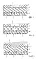
- FIG. 1is a cross-sectional view of a conventional semiconductor device at a preliminary stage of production.
- FIG. 2is a cross-sectional view of the semiconductor device of FIG. 1 at a subsequent stage of production.
- FIG. 3is a cross-sectional view of the semiconductor device of FIG. 2 at a subsequent stage of production.
- FIG. 4is a cross-sectional view of the semiconductor device of FIG. 3 at a subsequent stage of production.
- FIG. 5is a cross-sectional view of a semiconductor device at a preliminary stage of production and in accordance with a first embodiment of the present invention.
- FIG. 6is a cross-sectional view of the semiconductor device of FIG. 5 at a subsequent stage of production.
- FIG. 7is a cross-sectional view of the semiconductor device of FIG. 5 at a subsequent stage of production.
- FIG. 8is a cross-sectional view of the semiconductor device of FIG. 5 at a subsequent stage of production.
- FIG. 9is a cross-sectional view of the semiconductor device of FIG. 5 at a subsequent stage of production.
- FIG. 10is a cross-sectional view of the semiconductor device of FIG. at a subsequent stage of production.
- FIG. 11is a cross-sectional view of the semiconductor device of FIG. 5 at a subsequent stage of production.
- FIG. 12is a cross-sectional view of the semiconductor device of FIG. 5 at a subsequent stage of production.
- FIG. 13is a cross-sectional view of the semiconductor device of FIG. 5 at a subsequent stage of production.
- FIG. 14is a cross-sectional view of the semiconductor device of FIG. 5 at a subsequent stage of production.
- FIG. 15is a cross-sectional view of a semiconductor device constructed in accordance with a second embodiment of the present invention.
- FIG. 16is a cross-sectional view of the semiconductor device of FIG. 15 at a subsequent stage of production.
- FIG. 17is a cross-sectional view of a semiconductor device constructed in accordance with a third embodiment of the present invention.
- FIG. 18illustrates a computer system having a memory cell with a copper damascene structure according to the present invention.
- substrateused in the following description may include any semiconductor-based structure that has a semiconductor surface.
- the termshould be understood to include silicon, silicon-on insulator (SOI), silicon-on sapphire (SOS), doped and undoped semiconductors, epitaxial layers of silicon supported by a base semiconductor foundation, and other semiconductor structures.
- the semiconductorneed not be silicon-based.
- the semiconductorcould be silicon-germanium, germanium, or gallium arsenide.
- copperis intended to include not only elemental copper, but also copper with other trace metals or in various alloyed combinations with other metals as known in the art, as long as such alloy retains the physical and chemical properties of copper.
- copperis also intended to include conductive oxides of copper.
- FIGS. 5 - 17illustrate the formation of copper damascene structures 100 , 200 , 300 (FIGS. 14, 16, 17 ) formed in accordance with exemplary embodiments of the present invention.
- FIG. 5depicts a portion of an insulating layer 51 formed over a semiconductor substrate 50 , on or within which a metal layer 52 has been formed.
- the metal layer 52represents a lower metal interconnect layer which is to be later interconnected with an upper copper interconnect layer.
- the metal layer 52may be formed of copper (Cu), but other conductive materials, such as tungsten (W) or aluminum (Al) and their alloys, may be used also.
- an intermetal dielectric layer 55is formed overlying the insulating layer 51 and the metal layer 52 .
- the intermetal dielectric layer 55is formed of a low-dielectric constant material to a thickness of about 2,000 Angstroms to 50,000 Angstroms, more preferably of about 5,000 Angstroms to 20,000 Angstroms.
- a low-dielectric constant materialis a material with a dielectric constant of less than about 4.
- the intermetal dielectric layer 55is a low-dielectric constant material which can be directly patterned, without using a photoresist material, and which may be formed by a method described by Kikkawa in Current and Future Low - k Dielectrics for Cu Interconnects, Technical Digests of IEDM, pp. 253-56 (2000), the disclosure of which is incorporated by reference herein. Kikkawa has demonstrated that fabrication of photo-resistive low-dielectric constant films, such as methylsilsesquiazane (MSZ) films, can eliminate photoresist coating, dry etching and etch stop layers.
- MSZmethylsilsesquiazane
- vias and/or holesare formed in methylsilsesquiazane (MSZ) films by direct patterning, such as direct EB (electron beam) or UV (ultra violet) lithography, without using photoresist or dry etching.
- direct patterningsuch as direct EB (electron beam) or UV (ultra violet) lithography, without using photoresist or dry etching.
- a methylsilsesquiazane (MSZ) film precursoris deposited on a silicon substrate by spin-coating at 2700 rpm and pre-baked at about 90° C. for about 10 minutes.
- EB lithographyis subsequently carried out with doses of about 3 ⁇ C/cm 2 to about 123 ⁇ C/cm 2 .
- UV (I-line) lithographyis carried out with doses of about 45 mJ/cm 2 to about 315 mJ/cm 2 .
- moisture absorptionis conducted at 25° C. and 50% relative humidity for about 10 minutes.
- Development of the methylsilsesquiazane (MSZ) filmis then carried out in a tetra-methyl-ammonium hydroxide (TMAH) solution.
- TMAHtetra-methyl-ammonium hydroxide
- the methylsilsesquiazane (MSZ) filmundergoes curing at 400° C. in a nitrogen ambient to be subsequently transformed into a methylsilsesquioxane (MSQ) film.
- Kikkawa et al.have observed that, during curing at 400° C. in the nitrogen ambient, the methylsilsesquiazane (MSZ) film undergoes photochemical reactions so that the resulting methylsilsesquioxane (MSQ) film comprises no Si—N bonds and only Si—O and Si—CH 3 bonds.
- the intermetal dielectric layer 55may be also formed of a conventional insulating oxide, such as silicon oxide (SiO 2 ), or other low-dielectric constant materials such as, for example, polyimide, spin-on-polymers (SOP), parylene, flare, polyarylethers, polytetrafluoroethylene, benzocyclobutene (BCB), SILK, fluorinated silicon oxide (FSG), NANOGLASS or hydrogen silsesquioxane, which have dielectric constants of less than about 4.
- a conventional insulating oxidesuch as silicon oxide (SiO 2 )
- other low-dielectric constant materialssuch as, for example, polyimide, spin-on-polymers (SOP), parylene, flare, polyarylethers, polytetrafluoroethylene, benzocyclobutene (BCB), SILK, fluorinated silicon oxide (FSG), NANOGLASS or hydrogen silsesquioxane, which have dielectric constants
- a first mask layer 58 having images of a via pattern 59is formed over the intermetal dielectric layer 55 for direct patterning.
- a via 65may be formed by etching through the intermetal dielectric layer 55 with an etchant.
- the etchant(not shown) may be selected in accordance with the characteristics of the intermetal dielectric layer 55 , so that the dielectric material is selectively etched until the etchant reaches the metal layer 52 .
- the etchantis a tetra-methyl-ammonium hydroxide (TMAH) solution.
- a trench 67(FIG. 10) is formed by employing a second mask layer 62 (FIG. 9) having images of a trench pattern 63 (FIG. 9) over the intermetal dielectric layer 55 .
- the trench pattern 63is then etched into the intermetal dielectric layer 55 using the mask layer 62 to form trench 67 , as shown in FIG. 10.
- the etching of the trench 67may be accomplished using the same etchant employed to form the via 65 (FIG. 8), which according to a preferred embodiment of the invention is a tetra-methyl-ammonium hydroxide (TMAH) solution.
- TMAHtetra-methyl-ammonium hydroxide
- the intermetal dielectric layer 55is formed of methylsilsesquiazane material and if UV lithography is employed, the methylsilsesquiazane (MSZ) material undergoes curing at 400° C. in a nitrogen ambient to be subsequently transformed into a methylsilsesquioxane (MSQ) film.
- MSZmethylsilsesquiazane
- a diffusion barrier layer 72(FIG. 11) is formed on the via 65 and the trench 67 to a thickness of about 50 Angstroms to about 200 Angstroms, more preferably of about 100 Angstroms.
- the diffusion barrier layer 72is formed of tungsten nitride (WN 2 ) by a method described by Klaus et al. in Atomic Layer Deposition of Tungsten Nitride Films Using Sequential Surface Reactions, J. of Electrochemical Soc., Vol. 147(3), pp. 1175-1181 (2000), the disclosure of which is incorporated by reference herein. Klaus et al. have demonstrated that tungsten nitride films deposited with atomic layer control using sequential surface reactions have a stoichiometry with low carbon (C) and oxygen (O) impurity concentrations which prevent the diffusion of copper at elevated temperatures.
- Ccarbon
- Ooxygen
- tungsten nitride filmsare deposited at a temperature of about 600-800K using an initial treatment of 10 mTorr Si 2 H 6 at 600K for about 5 minutes on a hydroxilated SiO 2 surface.
- tungsten nitride film growthcan be conducted at reactions temperatures between about 550-800K by employing, for example, cycles of WF 6 and NH 3 to transform the SiO 2 surface to a tungsten nitride surface.
- the tungsten nitride films formed by the above-described atomic layer control using sequential surface reactions techniquehave a microcrystalline structure and a remarkably flat surface indicating smooth film growth.
- the tungsten nitride diffusion barrier layer 72is simultaneously deposited in both the via 65 and the trench 67 (FIG. 11), the invention is not limited to this embodiment.
- the tungsten-nitride diffusion barrier layer 72may be deposited first in the via 65 before the formation of the trench 67 , and then in the trench 67 after its respective formation.
- horizontal portions of the tungsten nitride material formed above the surface of the intermetal dielectric layer 55are removed by a light polishing technique to form the structure illustrated in FIG. 12.
- a light chemical mechanical polishingis used to polish away excess tungsten-nitride material above the intermetal dielectric layer 55 and the trench level. This way, the intermetal dielectric layer 55 acts as a polishing stop layer when light CMP is used.
- a conductive material 80 comprising copper (Cu)is next deposited to fill in both the via 65 and the trench 67 .
- the copperis selectively deposited by CVD as described by Kaloyeros et al. in Blanket And Selective Copper CVD From Cu ( fod ) 2 For Multilevel Metallization, Mat. Res. Soc. Symp. Proc., Vol. 181 (1990), the disclosure of which is incorporated by reference herein.
- LTMOCVDblanket and selective low-temperature metal-organic chemical vapor deposition
- the reactoris first pumped down to a base pressure of less than 5 ⁇ 10 ⁇ 7 torr. Subsequently, the source compound is introduced into the sublimator which is heated to 40-75° C. A mass flow controller is employed to control the flow of the mixed gas/precursor into the reactor.
- Copper depositionis carried out using argon (Ar) and hydrogen (H 2 ) as the carrier gases.
- the substrate 50is heated to about 300-400° C., while the pressure during deposition ranges from about 1 torr to about 10 torr, at a gas flow range of about 30 sccm to about 55 sccm.
- CMPchemical mechanical polishing
- the selective deposition of copper by CVDthat was described above is not the only method that could be employed for forming the conductive material 80 .
- coppercan be selectively deposited by an electroless plating technique, which is more attractive than conventional electroplating methods.
- electroless platingAccording to studies done by Shacham-Diamand et al. printed in Copper electroless deposition technology for ultra - large - scale - integration ( ULSI ) metallization , Microelectronic Engineering, Vol. 33, pp. 47-58 (1997), the disclosure of which is incorporated by reference herein, elecroless plating has a very high selectivity, excellent step coverage and good via/trench filling because of the very thin seed layers formed by this method. Electroless plating is also more advantageous than electroplating because of the low cost of tools and materials.
- contact displacement copper depositionis used to first selectively activate the tungsten nitride diffusion barrier layer 72 , after which selective electroless copper deposition is employed to obtain a copper layer 81 (FIG. 15). Copper deposition by contact displacement offers the advantage of room temperature, which in turn allows many low dielectric constant organic and/or inorganic materials to be used as the material of choice for interlayer dielectrics, such as the intermetal dielectric layer 55 .
- excess copper formed above the surface of the intermetal dielectric layer 55may be removed by either an etching or a polishing technique to form a copper dual damascene structure 200 illustrated in FIG. 16.
- CMPchemical mechanical polishing
- FIG. 14 and FIG. 16respectively, it must be readily apparent to those skilled in the art that in fact any number of such copper dual damascene structures may be formed on the substrate 50 .
- the exemplary embodiments described aboverefer to the formation of a copper dual damascene structure 100 , 200
- the inventionis further applicable to other types of damascene structures, for example triple damascene structures, as long as they include a tungsten nitride diffusion barrier layer and copper selectively deposited by the methods described in detail above.
- FIG. 17illustrates a triple damascene structure 300 formed within the intermetal dielectric layer 55 and over the substrate 50 , and in which vias and trenches are filled simultaneously with the selectively deposited copper by the methods described above.
- the interconnect structure of the inventionmay be used in the upper layer metallization patterns of many integrated circuit devices including, but not limited to, memory devices and processors.
- FIG. 18illustrates a typical processor-based system 400 which includes a memory circuit 448 , for example a DRAM memory circuit employing a plurality of DRAM memory devices.
- memory circuit 448for example a DRAM memory circuit employing a plurality of DRAM memory devices.
- CPUcentral processing unit
- DRAM memory devicemay contain damascene structures, such as the copper damascene structures 100 , 200 , 300 fabricated according to the present invention.
- a processor systemsuch as a computer system, generally comprises the central processing unit (CPU) 444 , such as a microprocessor, a digital signal processor, or other programmable digital logic devices, which communicates with an input/output (I/O) device 446 over a bus 452 .
- the memory 448communicates with the system over bus 452 .
- the processor systemmay include peripheral devices such as a floppy disk drive 454 and a compact disk (CD) ROM drive 456 which also communicate with CPU 444 over the bus 452 .
- Memory 448is preferably constructed as an integrated circuit, which includes one or more copper damascene structures 100 , 200 , 300 . If desired, the memory 448 may be combined with the processor, for example CPU 444 , in a single integrated circuit.
Landscapes
- Engineering & Computer Science (AREA)
- Physics & Mathematics (AREA)
- Condensed Matter Physics & Semiconductors (AREA)
- General Physics & Mathematics (AREA)
- Manufacturing & Machinery (AREA)
- Computer Hardware Design (AREA)
- Microelectronics & Electronic Packaging (AREA)
- Power Engineering (AREA)
- Chemical & Material Sciences (AREA)
- Chemical Kinetics & Catalysis (AREA)
- General Chemical & Material Sciences (AREA)
- Internal Circuitry In Semiconductor Integrated Circuit Devices (AREA)
Abstract
Description
- The present invention relates to the field of semiconductors and, in particular, to a method of forming damascene structures in semiconductor devices.[0001]
- In an attempt to improve the performance, reliability and density of fully integrated ULSI (ultra-large scale integration) interconnects, the microelectronics industry has recently begun migrating away from the use of aluminum (Al) and/or its alloys for the ULSI interconnects. As such, advanced dual damascene processes have begun using copper (Cu) as the material of choice because copper has high conductivity, extremely low resistivity (about 1.7 μΩcm) and good resistance to electromigration. Unfortunately, copper diffuses rapidly through silicon dioxide (SiO[0002]2) or other interlayer dielectrics, such as polyimides and parylenes, and copper diffusion can destroy active devices, such as transistors and capacitors, formed in the IC substrate. In addition, metal adhesion to the underlying substrate materials must be excellent to form reliable interconnect structures but the adhesion of copper to interlayer dielectrics, particularly to SiO2, is generally poor.
- Another problem associated with dual damascene processing is the cost and complexity of the process. Advanced copper dual damascene processes include a two-step sequential mask/etch process to form a two-level structure, such as a via connected to a metal line situated above the via. As illustrated in FIG. 1, a known copper dual damascene process as applied to interconnect formation begins with the deposition of a first[0003]
insulating layer 14 over a first levelinterconnect copper layer 12, which in turn is formed over or within asemiconductor substrate 10. A secondinsulating layer 16 is next formed over the first insulatinglayer 14. Anetch stop layer 15 is typically formed between the first and secondinsulating layers insulating layer 16 is patterned by photolithography with a first mask (not shown) to form atrench 17 corresponding to a copper line of a second level interconnect. Theetch stop layer 15 prevents the upperlevel trench pattern 17 from being etched through the firstinsulating layer 14. - As illustrated in FIG. 2, a second masking step followed by an etch step are applied to form a via[0004]18 through the
etch stop layer 15 and thefirst insulating layer 14. After the etching is completed, both thetrench 17 and thevia 18 are filled withcopper material 20, as illustrated in FIG. 3. Typically, thecopper material 20 undergoes a chemical mechanical polishing (CMP) step to remove any copper material from above the secondinsulating layer 16 and to form, therefore, a copper damascene structure as illustrated in FIG. 4. The CMP step leaves thecopper damascene structure 25 with a copper planarized surface for subsequent metallization to build multi-level interconnects. - If desired, a second etch stop layer (not shown) may be formed between the[0005]
substrate 10 and the firstinsulating layer 14 during the formation of thecopper damascene structure 25. In any event, and in contrast to a single damascene process, the via and the trench are simultaneously filled with metal. Thus, although copper dual damascene process is more advantageous over the copper single damascene process, one big disadvantage remains the high number of sequential photoresist/mask/etch steps and etch-stop layers which, as described above, are conventionally used in damascene processing and which increase the fabrication cost and reduce the production yield. Another disadvantage is that copper deposition methods for conventional damascene processes employ a large amount of high-purity copper material, of which a considerable amount is removed and wasted by the CMP process described above with reference to FIGS.3-4. Thus, even the dual damascene processing is very expensive and entails a large number of processing steps. - Accordingly, there is a need for an improved and simplified copper damascene process which reduces production costs and increases productivity. There is also a need for a method of increasing the adhesion of copper to underlying damascene layers as well as a method of decreasing copper diffusion in such layers.[0006]
- The present invention provides a method for fabricating a copper interconnect structure in a semiconductor device which requires fewer processing steps and reduces the diffusion of copper atoms to underlying damascene layers.[0007]
- In an exemplary embodiment, trenches and vias are formed by direct patterning of a low-dielectric constant material, subsequent to which a thin tungsten nitride (WN[0008]2) diffusion barrier layer is formed by an atomic layer deposition using sequential surface reactions inside the trenches and vias. A selective copper CVD process is used to fill in the trenches and vias with copper. In another exemplary embodiment, an electroless deposition technique is employed in lieu of the selective copper CVD process. This way, the sequential photoresist/mask/etch steps and the etch-stop layers are eliminated, while the diffusion of copper atoms into adjacent interconnect layers is suppressed.
- Additional advantages of the present invention will be more apparent from the detailed description and accompanying drawings, which illustrate preferred embodiments of the invention.[0009]
- FIG. 1 is a cross-sectional view of a conventional semiconductor device at a preliminary stage of production.[0010]
- FIG. 2 is a cross-sectional view of the semiconductor device of FIG. 1 at a subsequent stage of production.[0011]
- FIG. 3 is a cross-sectional view of the semiconductor device of FIG. 2 at a subsequent stage of production.[0012]
- FIG. 4 is a cross-sectional view of the semiconductor device of FIG. 3 at a subsequent stage of production.[0013]
- FIG. 5 is a cross-sectional view of a semiconductor device at a preliminary stage of production and in accordance with a first embodiment of the present invention.[0014]
- FIG. 6 is a cross-sectional view of the semiconductor device of FIG. 5 at a subsequent stage of production.[0015]
- FIG. 7 is a cross-sectional view of the semiconductor device of FIG. 5 at a subsequent stage of production.[0016]
- FIG. 8 is a cross-sectional view of the semiconductor device of FIG. 5 at a subsequent stage of production.[0017]
- FIG. 9 is a cross-sectional view of the semiconductor device of FIG. 5 at a subsequent stage of production.[0018]
- FIG. 10 is a cross-sectional view of the semiconductor device of FIG. at a subsequent stage of production.[0019]
- FIG. 11 is a cross-sectional view of the semiconductor device of FIG. 5 at a subsequent stage of production.[0020]
- FIG. 12 is a cross-sectional view of the semiconductor device of FIG. 5 at a subsequent stage of production.[0021]
- FIG. 13 is a cross-sectional view of the semiconductor device of FIG. 5 at a subsequent stage of production.[0022]
- FIG. 14 is a cross-sectional view of the semiconductor device of FIG. 5 at a subsequent stage of production.[0023]
- FIG. 15 is a cross-sectional view of a semiconductor device constructed in accordance with a second embodiment of the present invention.[0024]
- FIG. 16 is a cross-sectional view of the semiconductor device of FIG. 15 at a subsequent stage of production.[0025]
- FIG. 17 is a cross-sectional view of a semiconductor device constructed in accordance with a third embodiment of the present invention.[0026]
- FIG. 18 illustrates a computer system having a memory cell with a copper damascene structure according to the present invention.[0027]
- In the following detailed description, reference is made to various specific embodiments in which the invention may be practiced. These embodiments are described with sufficient detail to enable those skilled in the art to practice the invention, and it is to be understood that other embodiments may be employed, and that structural, electrical and process changes may be made without departing from the spirit or scope of the present invention.[0028]
- The term “substrate” used in the following description may include any semiconductor-based structure that has a semiconductor surface. The term should be understood to include silicon, silicon-on insulator (SOI), silicon-on sapphire (SOS), doped and undoped semiconductors, epitaxial layers of silicon supported by a base semiconductor foundation, and other semiconductor structures. The semiconductor need not be silicon-based. The semiconductor could be silicon-germanium, germanium, or gallium arsenide. When reference is made to a “substrate” in the following description, previous process steps may have been utilized to form regions or junctions in or on the base semiconductor or foundation.[0029]
- The term “copper” is intended to include not only elemental copper, but also copper with other trace metals or in various alloyed combinations with other metals as known in the art, as long as such alloy retains the physical and chemical properties of copper. The term “copper” is also intended to include conductive oxides of copper.[0030]
- Referring now to the drawings, where like elements are designated by like reference numerals, FIGS.[0031]5-17 illustrate the formation of copper
damascene structures insulating layer 51 formed over asemiconductor substrate 50, on or within which ametal layer 52 has been formed. Themetal layer 52 represents a lower metal interconnect layer which is to be later interconnected with an upper copper interconnect layer. Themetal layer 52 may be formed of copper (Cu), but other conductive materials, such as tungsten (W) or aluminum (Al) and their alloys, may be used also. - Referring now to FIG. 6, an[0032]
intermetal dielectric layer 55 is formed overlying the insulatinglayer 51 and themetal layer 52. In an exemplary embodiment of the present invention, theintermetal dielectric layer 55 is formed of a low-dielectric constant material to a thickness of about 2,000 Angstroms to 50,000 Angstroms, more preferably of about 5,000 Angstroms to 20,000 Angstroms. For the purposes of the present invention, a low-dielectric constant material is a material with a dielectric constant of less than about 4. - In a preferred embodiment of the invention, the[0033]
intermetal dielectric layer 55 is a low-dielectric constant material which can be directly patterned, without using a photoresist material, and which may be formed by a method described by Kikkawa inCurrent and Future Low-k Dielectrics for Cu Interconnects,Technical Digests of IEDM, pp. 253-56 (2000), the disclosure of which is incorporated by reference herein. Kikkawa has demonstrated that fabrication of photo-resistive low-dielectric constant films, such as methylsilsesquiazane (MSZ) films, can eliminate photoresist coating, dry etching and etch stop layers. According to recent experiments conducted by Kikkawa, vias and/or holes are formed in methylsilsesquiazane (MSZ) films by direct patterning, such as direct EB (electron beam) or UV (ultra violet) lithography, without using photoresist or dry etching. - According to the experiments conducted by Kikkawa, a methylsilsesquiazane (MSZ) film precursor is deposited on a silicon substrate by spin-coating at 2700 rpm and pre-baked at about 90° C. for about 10 minutes. EB lithography is subsequently carried out with doses of about 3 μC/cm[0034]2to about 123 μC/cm2. Alternatively, UV (I-line) lithography is carried out with doses of about 45 mJ/cm2to about 315 mJ/cm2. For either the UV or the EB lithography, moisture absorption is conducted at 25° C. and 50% relative humidity for about 10 minutes. Development of the methylsilsesquiazane (MSZ) film is then carried out in a tetra-methyl-ammonium hydroxide (TMAH) solution.
- If UV lithography is employed, the methylsilsesquiazane (MSZ) film undergoes curing at 400° C. in a nitrogen ambient to be subsequently transformed into a methylsilsesquioxane (MSQ) film. Kikkawa et al. have observed that, during curing at 400° C. in the nitrogen ambient, the methylsilsesquiazane (MSZ) film undergoes photochemical reactions so that the resulting methylsilsesquioxane (MSQ) film comprises no Si—N bonds and only Si—O and Si—CH[0035]3bonds.
- Although low-dielectric constant materials such as the methylsilsesquiazane (MSZ) films are preferred, the present invention is not limited to these materials. Thus, the[0036]
intermetal dielectric layer 55 may be also formed of a conventional insulating oxide, such as silicon oxide (SiO2), or other low-dielectric constant materials such as, for example, polyimide, spin-on-polymers (SOP), parylene, flare, polyarylethers, polytetrafluoroethylene, benzocyclobutene (BCB), SILK, fluorinated silicon oxide (FSG), NANOGLASS or hydrogen silsesquioxane, which have dielectric constants of less than about 4. - Next, as illustrated in FIG. 7, a[0037]
first mask layer 58 having images of a via pattern59 is formed over theintermetal dielectric layer 55 for direct patterning. - Thus, as shown in FIG. 8, a via[0038]65 may be formed by etching through the
intermetal dielectric layer 55 with an etchant. The etchant (not shown) may be selected in accordance with the characteristics of theintermetal dielectric layer 55, so that the dielectric material is selectively etched until the etchant reaches themetal layer 52. As noted above, and according to a preferred embodiment, the etchant is a tetra-methyl-ammonium hydroxide (TMAH) solution. - After the formation of the via[0039]65 through the
intermetal dielectric layer 55, a trench67 (FIG. 10) is formed by employing a second mask layer62 (FIG. 9) having images of a trench pattern63 (FIG. 9) over theintermetal dielectric layer 55. Thetrench pattern 63 is then etched into theintermetal dielectric layer 55 using themask layer 62 to formtrench 67, as shown in FIG. 10. The etching of thetrench 67 may be accomplished using the same etchant employed to form the via65 (FIG. 8), which according to a preferred embodiment of the invention is a tetra-methyl-ammonium hydroxide (TMAH) solution. - As noted above, if the[0040]
intermetal dielectric layer 55 is formed of methylsilsesquiazane material and if UV lithography is employed, the methylsilsesquiazane (MSZ) material undergoes curing at 400° C. in a nitrogen ambient to be subsequently transformed into a methylsilsesquioxane (MSQ) film. - Subsequent to the formation of[0041]
trench 67, thesecond mask layer 62 is removed so that further steps to create the copper dual damascene structure100 (FIG. 14) may be carried out. As such, a diffusion barrier layer72 (FIG. 11) is formed on the via65 and thetrench 67 to a thickness of about 50 Angstroms to about 200 Angstroms, more preferably of about 100 Angstroms. - In a preferred embodiment, the[0042]
diffusion barrier layer 72 is formed of tungsten nitride (WN2) by a method described by Klaus et al. inAtomic Layer Deposition of Tungsten Nitride Films Using Sequential Surface Reactions,J. of Electrochemical Soc., Vol. 147(3), pp. 1175-1181 (2000), the disclosure of which is incorporated by reference herein. Klaus et al. have demonstrated that tungsten nitride films deposited with atomic layer control using sequential surface reactions have a stoichiometry with low carbon (C) and oxygen (O) impurity concentrations which prevent the diffusion of copper at elevated temperatures. According to the atomic layer control using sequential surface reactions technique described by Klaus et al., tungsten nitride films are deposited at a temperature of about 600-800K using an initial treatment of 10 mTorr Si2H6at 600K for about 5 minutes on a hydroxilated SiO2surface. After the initial Si2H6treatment, tungsten nitride film growth can be conducted at reactions temperatures between about 550-800K by employing, for example, cycles of WF6and NH3to transform the SiO2surface to a tungsten nitride surface. The tungsten nitride films formed by the above-described atomic layer control using sequential surface reactions technique have a microcrystalline structure and a remarkably flat surface indicating smooth film growth. - Although in a preferred embodiment of the invention the tungsten nitride[0043]
diffusion barrier layer 72 is simultaneously deposited in both the via65 and the trench67 (FIG. 11), the invention is not limited to this embodiment. Thus, the tungsten-nitridediffusion barrier layer 72 may be deposited first in the via65 before the formation of thetrench 67, and then in thetrench 67 after its respective formation. In any event, after the formation of thediffusion barrier layer 72, horizontal portions of the tungsten nitride material formed above the surface of theintermetal dielectric layer 55 are removed by a light polishing technique to form the structure illustrated in FIG. 12. In a preferred embodiment of the present invention, a light chemical mechanical polishing (CMP) is used to polish away excess tungsten-nitride material above theintermetal dielectric layer 55 and the trench level. This way, theintermetal dielectric layer 55 acts as a polishing stop layer when light CMP is used. - As illustrated in FIG. 13, a[0044]
conductive material 80 comprising copper (Cu) is next deposited to fill in both the via65 and thetrench 67. In an exemplary embodiment, the copper is selectively deposited by CVD as described by Kaloyeros et al. inBlanket And Selective Copper CVD From Cu(fod)2For Multilevel Metallization,Mat. Res. Soc. Symp. Proc., Vol. 181 (1990), the disclosure of which is incorporated by reference herein. Studies of blanket and selective low-temperature metal-organic chemical vapor deposition (LTMOCVD) of copper have been conducted by Kaloyeros et al. at 300-400° C. in an atmosphere of pure H2or Ar from the β-diketonate precursor bis(6,6,7,8,8,8×-heptafluoro-2,2-dimetyl 1-3,5-octanedino) copper (II), Cu (fod)2. According to one selective LTMOCVD technique proposed by Kaloyeros et al., the reactor is first pumped down to a base pressure of less than 5×10⁻⁷torr. Subsequently, the source compound is introduced into the sublimator which is heated to 40-75° C. A mass flow controller is employed to control the flow of the mixed gas/precursor into the reactor. Copper deposition is carried out using argon (Ar) and hydrogen (H2) as the carrier gases. Thesubstrate 50 is heated to about 300-400° C., while the pressure during deposition ranges from about 1 torr to about 10 torr, at a gas flow range of about 30 sccm to about 55 sccm. - After the deposition of the[0045]
copper material 80, excess copper formed above the surface of theintermetal dielectric layer 55 may be removed by either an etching or a polishing technique to form the copperdual damascene structure 100 illustrated in FIG. 14. In a preferred embodiment of the present invention, chemical mechanical polishing (CMP) is used to polish away excess copper above theintermetal dielectric layer 55 and the trench level. This way, theintermetal dielectric layer 55 acts as a polishing stop layer when CMP is used. - The selective deposition of copper by CVD that was described above is not the only method that could be employed for forming the[0046]
conductive material 80. For example, according to another embodiment of the invention, copper can be selectively deposited by an electroless plating technique, which is more attractive than conventional electroplating methods. According to studies done by Shacham-Diamand et al. printed inCopper electroless deposition technology for ultra-large-scale-integration(ULSI)metallization, Microelectronic Engineering, Vol. 33, pp. 47-58 (1997), the disclosure of which is incorporated by reference herein, elecroless plating has a very high selectivity, excellent step coverage and good via/trench filling because of the very thin seed layers formed by this method. Electroless plating is also more advantageous than electroplating because of the low cost of tools and materials. - According to Shacham-Diamand et al., three practical seeding methods for the electroless deposition of copper could be used: (1) noble metal seeding, typically on gold, palladium or platinum; (2) copper seeding using an aluminum sacrificial layer; and (3) wet activation of surfaces using a contact displacement method. Shacham-Diamand et al. have successfully used the third method to deposit copper on Ti/TiN or TiN/AlCu at room temperature. Accordingly, in an exemplary embodiment of the present invention, contact displacement copper deposition is used to first selectively activate the tungsten nitride[0047]
diffusion barrier layer 72, after which selective electroless copper deposition is employed to obtain a copper layer81 (FIG. 15). Copper deposition by contact displacement offers the advantage of room temperature, which in turn allows many low dielectric constant organic and/or inorganic materials to be used as the material of choice for interlayer dielectrics, such as theintermetal dielectric layer 55. - After the deposition of the copper material[0048]81 (FIG. 15), excess copper formed above the surface of the
intermetal dielectric layer 55 may be removed by either an etching or a polishing technique to form a copperdual damascene structure 200 illustrated in FIG. 16. In a preferred embodiment of the present invention, chemical mechanical polishing (CMP) is used to polish away excess copper above theintermetal dielectric layer 55 and the trench level. This way, theintermetal dielectric layer 55 acts as a polishing stop layer when CMP is used. - Although only one copper[0049]
dual damascene structure substrate 50. Also, although the exemplary embodiments described above refer to the formation of a copperdual damascene structure damascene structure 300 formed within theintermetal dielectric layer 55 and over thesubstrate 50, and in which vias and trenches are filled simultaneously with the selectively deposited copper by the methods described above. - In addition, further steps to create a functional semiconductor circuit structure may be carried out. Thus, additional multilevel interconnect layers and associated dielectric layers could be formed to create operative electrical paths from any of the[0050]
copper damascene structures substrate 50. - The interconnect structure of the invention may be used in the upper layer metallization patterns of many integrated circuit devices including, but not limited to, memory devices and processors. FIG. 18 illustrates a typical processor-based[0051]
system 400 which includes amemory circuit 448, for example a DRAM memory circuit employing a plurality of DRAM memory devices. One or both of central processing unit (CPU)444 and the DRAM memory device may contain damascene structures, such as thecopper damascene structures device 446 over abus 452. Thememory 448 communicates with the system overbus 452. - In the case of a computer system, the processor system may include peripheral devices such as a[0052]
floppy disk drive 454 and a compact disk (CD)ROM drive 456 which also communicate withCPU 444 over thebus 452.Memory 448 is preferably constructed as an integrated circuit, which includes one or morecopper damascene structures memory 448 may be combined with the processor, forexample CPU 444, in a single integrated circuit. - The above description and drawings are only to be considered illustrative of exemplary embodiments which achieve the features and advantages of the present invention. Modification and substitutions to specific process conditions and structures can be made without departing from the spirit and scope of the present invention. Accordingly, the invention is not to be considered as being limited by the foregoing description and drawings, but is only limited by the scope of the appended claims.[0053]
Claims (45)
Priority Applications (2)
| Application Number | Priority Date | Filing Date | Title |
|---|---|---|---|
| US09/910,914US6919266B2 (en) | 2001-07-24 | 2001-07-24 | Copper technology for ULSI metallization |
| US10/109,713US20030020169A1 (en) | 2001-07-24 | 2002-04-01 | Copper technology for ULSI metallization |
Applications Claiming Priority (1)
| Application Number | Priority Date | Filing Date | Title |
|---|---|---|---|
| US09/910,914US6919266B2 (en) | 2001-07-24 | 2001-07-24 | Copper technology for ULSI metallization |
Related Child Applications (1)
| Application Number | Title | Priority Date | Filing Date |
|---|---|---|---|
| US10/109,713DivisionUS20030020169A1 (en) | 2001-07-24 | 2002-04-01 | Copper technology for ULSI metallization |
Publications (2)
| Publication Number | Publication Date |
|---|---|
| US20030020180A1true US20030020180A1 (en) | 2003-01-30 |
| US6919266B2 US6919266B2 (en) | 2005-07-19 |
Family
ID=25429490
Family Applications (2)
| Application Number | Title | Priority Date | Filing Date |
|---|---|---|---|
| US09/910,914Expired - Fee RelatedUS6919266B2 (en) | 2001-07-24 | 2001-07-24 | Copper technology for ULSI metallization |
| US10/109,713AbandonedUS20030020169A1 (en) | 2001-07-24 | 2002-04-01 | Copper technology for ULSI metallization |
Family Applications After (1)
| Application Number | Title | Priority Date | Filing Date |
|---|---|---|---|
| US10/109,713AbandonedUS20030020169A1 (en) | 2001-07-24 | 2002-04-01 | Copper technology for ULSI metallization |
Country Status (1)
| Country | Link |
|---|---|
| US (2) | US6919266B2 (en) |
Cited By (37)
| Publication number | Priority date | Publication date | Assignee | Title |
|---|---|---|---|---|
| US20020122885A1 (en)* | 2001-03-01 | 2002-09-05 | Micron Technology, Inc. | Methods, systems, and apparatus for uniform chemical-vapor depositions |
| US20030122246A1 (en)* | 2001-12-31 | 2003-07-03 | Mou-Shiung Lin | Integrated chip package structure using silicon substrate and method of manufacturing the same |
| US20030207032A1 (en)* | 2002-05-02 | 2003-11-06 | Micron Technology, Inc. | Methods, systems, and apparatus for atomic-layer deposition of aluminum oxides in integrated circuits |
| US20030227033A1 (en)* | 2002-06-05 | 2003-12-11 | Micron Technology, Inc. | Atomic layer-deposited HfA1O3 films for gate dielectrics |
| US6716741B2 (en)* | 2002-04-09 | 2004-04-06 | United Microelectronics Corp. | Method of patterning dielectric layer with low dielectric constant |
| US20050023584A1 (en)* | 2002-05-02 | 2005-02-03 | Micron Technology, Inc. | Atomic layer deposition and conversion |
| US20050023594A1 (en)* | 2002-06-05 | 2005-02-03 | Micron Technology, Inc. | Pr2O3-based la-oxide gate dielectrics |
| US20050023626A1 (en)* | 2003-06-24 | 2005-02-03 | Micron Technology, Inc. | Lanthanide oxide / hafnium oxide dielectrics |
| US20050029547A1 (en)* | 2003-06-24 | 2005-02-10 | Micron Technology, Inc. | Lanthanide oxide / hafnium oxide dielectric layers |
| US20050037603A1 (en)* | 2003-08-12 | 2005-02-17 | Stmicroelectronics S.A. | Method for forming, under a thin layer of a first material, portions of another material and/or empty areas |
| US6900541B1 (en)* | 2004-02-10 | 2005-05-31 | United Microelectronics Corp. | Semiconductor chip capable of implementing wire bonding over active circuits |
| US20050277256A1 (en)* | 2002-07-30 | 2005-12-15 | Micron Technology, Inc. | Nanolaminates of hafnium oxide and zirconium oxide |
| US20060043504A1 (en)* | 2004-08-31 | 2006-03-02 | Micron Technology, Inc. | Atomic layer deposited titanium aluminum oxide films |
| US20060043492A1 (en)* | 2004-08-26 | 2006-03-02 | Micron Technology, Inc. | Ruthenium gate for a lanthanide oxide dielectric layer |
| US20060046471A1 (en)* | 2004-08-27 | 2006-03-02 | Kirby Kyle K | Methods for forming vias of varying lateral dimensions and semiconductor components and assemblies including same |
| US20060046522A1 (en)* | 2004-08-31 | 2006-03-02 | Micron Technology, Inc. | Atomic layer deposited lanthanum aluminum oxide dielectric layer |
| US20060128168A1 (en)* | 2004-12-13 | 2006-06-15 | Micron Technology, Inc. | Atomic layer deposited lanthanum hafnium oxide dielectrics |
| US20060141777A1 (en)* | 2004-12-23 | 2006-06-29 | Yeong-Sil Kim | Methods for patterning a layer of a semiconductor device |
| US20060226547A1 (en)* | 2004-02-10 | 2006-10-12 | Kun-Chih Wang | Semiconductor chip capable of implementing wire bonding over active circuits |
| US20060244082A1 (en)* | 2005-04-28 | 2006-11-02 | Micron Technology, Inc. | Atomic layer desposition of a ruthenium layer to a lanthanide oxide dielectric layer |
| US20060270147A1 (en)* | 2005-05-27 | 2006-11-30 | Micron Technology, Inc. | Hafnium titanium oxide films |
| US20060273466A1 (en)* | 2005-06-06 | 2006-12-07 | Nguyen Huong T | Adhesion of tungsten nitride films to a silicon surface |
| US20070049023A1 (en)* | 2005-08-29 | 2007-03-01 | Micron Technology, Inc. | Zirconium-doped gadolinium oxide films |
| US20070049054A1 (en)* | 2005-08-31 | 2007-03-01 | Micron Technology, Inc. | Cobalt titanium oxide dielectric films |
| US20070048926A1 (en)* | 2005-08-31 | 2007-03-01 | Micron Technology, Inc. | Lanthanum aluminum oxynitride dielectric films |
| US20070059881A1 (en)* | 2003-03-31 | 2007-03-15 | Micron Technology, Inc. | Atomic layer deposited zirconium aluminum oxide |
| US20070085209A1 (en)* | 2005-10-18 | 2007-04-19 | Taiwan Semiconductor Manufacturing Co., Ltd. | Anchored damascene structures |
| US20070232051A1 (en)* | 2006-03-16 | 2007-10-04 | Advanced Semiconductor Engineering Inc. | Method for forming metal bumps |
| US7405454B2 (en) | 2003-03-04 | 2008-07-29 | Micron Technology, Inc. | Electronic apparatus with deposited dielectric layers |
| US20090011542A1 (en)* | 2001-03-30 | 2009-01-08 | Megica Corporation | Structure and manufactruing method of chip scale package |
| US7728626B2 (en) | 2002-07-08 | 2010-06-01 | Micron Technology, Inc. | Memory utilizing oxide nanolaminates |
| US20110205720A1 (en)* | 2001-12-31 | 2011-08-25 | Megica Corporation | Integrated chip package structure using organic substrate and method of manufacturing the same |
| US8492870B2 (en) | 2002-01-19 | 2013-07-23 | Megica Corporation | Semiconductor package with interconnect layers |
| US8501563B2 (en) | 2005-07-20 | 2013-08-06 | Micron Technology, Inc. | Devices with nanocrystals and methods of formation |
| US8535976B2 (en) | 2001-12-31 | 2013-09-17 | Megica Corporation | Method for fabricating chip package with die and substrate |
| US10199267B2 (en)* | 2017-06-30 | 2019-02-05 | Lam Research Corporation | Tungsten nitride barrier layer deposition |
| CN114203557A (en)* | 2021-11-23 | 2022-03-18 | 江苏东海半导体科技有限公司 | Semiconductor device fabrication method, device and storage medium |
Families Citing this family (17)
| Publication number | Priority date | Publication date | Assignee | Title |
|---|---|---|---|---|
| US7476925B2 (en) | 2001-08-30 | 2009-01-13 | Micron Technology, Inc. | Atomic layer deposition of metal oxide and/or low asymmetrical tunnel barrier interploy insulators |
| US7068544B2 (en) | 2001-08-30 | 2006-06-27 | Micron Technology, Inc. | Flash memory with low tunnel barrier interpoly insulators |
| US8026161B2 (en) | 2001-08-30 | 2011-09-27 | Micron Technology, Inc. | Highly reliable amorphous high-K gate oxide ZrO2 |
| US7221017B2 (en) | 2002-07-08 | 2007-05-22 | Micron Technology, Inc. | Memory utilizing oxide-conductor nanolaminates |
| US6884739B2 (en) | 2002-08-15 | 2005-04-26 | Micron Technology Inc. | Lanthanide doped TiOx dielectric films by plasma oxidation |
| US7199023B2 (en) | 2002-08-28 | 2007-04-03 | Micron Technology, Inc. | Atomic layer deposited HfSiON dielectric films wherein each precursor is independendently pulsed |
| US7084078B2 (en) | 2002-08-29 | 2006-08-01 | Micron Technology, Inc. | Atomic layer deposited lanthanide doped TiOx dielectric films |
| JP2004146691A (en)* | 2002-10-25 | 2004-05-20 | Chi Mei Electronics Corp | Method for forming microcrystalline thin film, method for manufacturing thin film transistor, thin film transistor, and image display device using thin film transistor |
| US7601649B2 (en) | 2004-08-02 | 2009-10-13 | Micron Technology, Inc. | Zirconium-doped tantalum oxide films |
| US7560395B2 (en) | 2005-01-05 | 2009-07-14 | Micron Technology, Inc. | Atomic layer deposited hafnium tantalum oxide dielectrics |
| US7374964B2 (en) | 2005-02-10 | 2008-05-20 | Micron Technology, Inc. | Atomic layer deposition of CeO2/Al2O3 films as gate dielectrics |
| US7687409B2 (en) | 2005-03-29 | 2010-03-30 | Micron Technology, Inc. | Atomic layer deposited titanium silicon oxide films |
| US8110469B2 (en) | 2005-08-30 | 2012-02-07 | Micron Technology, Inc. | Graded dielectric layers |
| US7709402B2 (en) | 2006-02-16 | 2010-05-04 | Micron Technology, Inc. | Conductive layers for hafnium silicon oxynitride films |
| JP2008085175A (en)* | 2006-09-28 | 2008-04-10 | Tokyo Electron Ltd | Semiconductor device manufacturing method, semiconductor device, substrate processing system, program, and storage medium |
| US7601604B2 (en)* | 2006-10-12 | 2009-10-13 | Atmel Corporation | Method for fabricating conducting plates for a high-Q MIM capacitor |
| CN110828372A (en)* | 2019-11-11 | 2020-02-21 | 武汉新芯集成电路制造有限公司 | Metal lead, semiconductor device and method of making the same |
Citations (4)
| Publication number | Priority date | Publication date | Assignee | Title |
|---|---|---|---|---|
| US6352938B2 (en)* | 1999-12-09 | 2002-03-05 | United Microelectronics Corp. | Method of removing photoresist and reducing native oxide in dual damascene copper process |
| US6395632B1 (en)* | 2000-08-31 | 2002-05-28 | Micron Technology, Inc. | Etch stop in damascene interconnect structure and method of making |
| US6498090B2 (en)* | 2000-02-03 | 2002-12-24 | Seiko Epson Corporation | Semiconductor devices and methods for manufacturing the same |
| US6531777B1 (en)* | 2000-06-22 | 2003-03-11 | Advanced Micro Devices, Inc. | Barrier metal integrity testing using a dual level line to line leakage testing pattern and partial CMP |
Family Cites Families (11)
| Publication number | Priority date | Publication date | Assignee | Title |
|---|---|---|---|---|
| US5380546A (en)* | 1993-06-09 | 1995-01-10 | Microelectronics And Computer Technology Corporation | Multilevel metallization process for electronic components |
| US6380083B1 (en)* | 1998-08-28 | 2002-04-30 | Agere Systems Guardian Corp. | Process for semiconductor device fabrication having copper interconnects |
| US6110648A (en)* | 1998-09-17 | 2000-08-29 | Taiwan Semiconductor Manufacturing Company | Method of enclosing copper conductor in a dual damascene process |
| US6010962A (en)* | 1999-02-12 | 2000-01-04 | Taiwan Semiconductor Manufacturing Company | Copper chemical-mechanical-polishing (CMP) dishing |
| TW400619B (en)* | 1999-03-05 | 2000-08-01 | United Microelectronics Corp | The manufacture method of dual damascene structure |
| US6329280B1 (en)* | 1999-05-13 | 2001-12-11 | International Business Machines Corporation | Interim oxidation of silsesquioxane dielectric for dual damascene process |
| US20020009880A1 (en)* | 1999-08-27 | 2002-01-24 | Qing-Tang Jiang | Metal barrier for copper interconnects that incorporates silicon in the metal barrier or at the copper/metal barrier interface |
| US6040243A (en)* | 1999-09-20 | 2000-03-21 | Chartered Semiconductor Manufacturing Ltd. | Method to form copper damascene interconnects using a reverse barrier metal scheme to eliminate copper diffusion |
| US6297158B1 (en)* | 2000-05-31 | 2001-10-02 | Taiwan Semiconductor Manufacturing Company | Stress management of barrier metal for resolving CU line corrosion |
| US6368954B1 (en)* | 2000-07-28 | 2002-04-09 | Advanced Micro Devices, Inc. | Method of copper interconnect formation using atomic layer copper deposition |
| US6451683B1 (en)* | 2000-08-28 | 2002-09-17 | Micron Technology, Inc. | Damascene structure and method of making |
- 2001
- 2001-07-24USUS09/910,914patent/US6919266B2/ennot_activeExpired - Fee Related
- 2002
- 2002-04-01USUS10/109,713patent/US20030020169A1/ennot_activeAbandoned
Patent Citations (4)
| Publication number | Priority date | Publication date | Assignee | Title |
|---|---|---|---|---|
| US6352938B2 (en)* | 1999-12-09 | 2002-03-05 | United Microelectronics Corp. | Method of removing photoresist and reducing native oxide in dual damascene copper process |
| US6498090B2 (en)* | 2000-02-03 | 2002-12-24 | Seiko Epson Corporation | Semiconductor devices and methods for manufacturing the same |
| US6531777B1 (en)* | 2000-06-22 | 2003-03-11 | Advanced Micro Devices, Inc. | Barrier metal integrity testing using a dual level line to line leakage testing pattern and partial CMP |
| US6395632B1 (en)* | 2000-08-31 | 2002-05-28 | Micron Technology, Inc. | Etch stop in damascene interconnect structure and method of making |
Cited By (105)
| Publication number | Priority date | Publication date | Assignee | Title |
|---|---|---|---|---|
| US20050087134A1 (en)* | 2001-03-01 | 2005-04-28 | Micron Technology, Inc. | Methods, systems, and apparatus for uniform chemical-vapor depositions |
| US6852167B2 (en) | 2001-03-01 | 2005-02-08 | Micron Technology, Inc. | Methods, systems, and apparatus for uniform chemical-vapor depositions |
| US7410668B2 (en) | 2001-03-01 | 2008-08-12 | Micron Technology, Inc. | Methods, systems, and apparatus for uniform chemical-vapor depositions |
| US20020122885A1 (en)* | 2001-03-01 | 2002-09-05 | Micron Technology, Inc. | Methods, systems, and apparatus for uniform chemical-vapor depositions |
| US8912666B2 (en) | 2001-03-30 | 2014-12-16 | Qualcomm Incorporated | Structure and manufacturing method of chip scale package |
| US9018774B2 (en) | 2001-03-30 | 2015-04-28 | Qualcomm Incorporated | Chip package |
| US8748227B2 (en) | 2001-03-30 | 2014-06-10 | Megit Acquisition Corp. | Method of fabricating chip package |
| US8426982B2 (en) | 2001-03-30 | 2013-04-23 | Megica Corporation | Structure and manufacturing method of chip scale package |
| US20090289346A1 (en)* | 2001-03-30 | 2009-11-26 | Megica Corporation | Structure and manufacturing method of chip scale package |
| US20090011542A1 (en)* | 2001-03-30 | 2009-01-08 | Megica Corporation | Structure and manufactruing method of chip scale package |
| US20090008778A1 (en)* | 2001-03-30 | 2009-01-08 | Megica Corporation | Structure and manufactruing method of chip scale package |
| US20030122246A1 (en)* | 2001-12-31 | 2003-07-03 | Mou-Shiung Lin | Integrated chip package structure using silicon substrate and method of manufacturing the same |
| US8471361B2 (en) | 2001-12-31 | 2013-06-25 | Megica Corporation | Integrated chip package structure using organic substrate and method of manufacturing the same |
| US9030029B2 (en)* | 2001-12-31 | 2015-05-12 | Qualcomm Incorporated | Chip package with die and substrate |
| US8835221B2 (en) | 2001-12-31 | 2014-09-16 | Qualcomm Incorporated | Integrated chip package structure using ceramic substrate and method of manufacturing the same |
| US9136246B2 (en) | 2001-12-31 | 2015-09-15 | Qualcomm Incorporated | Integrated chip package structure using silicon substrate and method of manufacturing the same |
| US20110205720A1 (en)* | 2001-12-31 | 2011-08-25 | Megica Corporation | Integrated chip package structure using organic substrate and method of manufacturing the same |
| US8535976B2 (en) | 2001-12-31 | 2013-09-17 | Megica Corporation | Method for fabricating chip package with die and substrate |
| US8492870B2 (en) | 2002-01-19 | 2013-07-23 | Megica Corporation | Semiconductor package with interconnect layers |
| US6716741B2 (en)* | 2002-04-09 | 2004-04-06 | United Microelectronics Corp. | Method of patterning dielectric layer with low dielectric constant |
| US7560793B2 (en) | 2002-05-02 | 2009-07-14 | Micron Technology, Inc. | Atomic layer deposition and conversion |
| US7160577B2 (en) | 2002-05-02 | 2007-01-09 | Micron Technology, Inc. | Methods for atomic-layer deposition of aluminum oxides in integrated circuits |
| US20030207032A1 (en)* | 2002-05-02 | 2003-11-06 | Micron Technology, Inc. | Methods, systems, and apparatus for atomic-layer deposition of aluminum oxides in integrated circuits |
| US20060000412A1 (en)* | 2002-05-02 | 2006-01-05 | Micron Technology, Inc. | Systems and apparatus for atomic-layer deposition |
| US7670646B2 (en) | 2002-05-02 | 2010-03-02 | Micron Technology, Inc. | Methods for atomic-layer deposition |
| US20050023584A1 (en)* | 2002-05-02 | 2005-02-03 | Micron Technology, Inc. | Atomic layer deposition and conversion |
| US7589029B2 (en) | 2002-05-02 | 2009-09-15 | Micron Technology, Inc. | Atomic layer deposition and conversion |
| US20050023594A1 (en)* | 2002-06-05 | 2005-02-03 | Micron Technology, Inc. | Pr2O3-based la-oxide gate dielectrics |
| US7205218B2 (en) | 2002-06-05 | 2007-04-17 | Micron Technology, Inc. | Method including forming gate dielectrics having multiple lanthanide oxide layers |
| US7554161B2 (en) | 2002-06-05 | 2009-06-30 | Micron Technology, Inc. | HfAlO3 films for gate dielectrics |
| US8093638B2 (en) | 2002-06-05 | 2012-01-10 | Micron Technology, Inc. | Systems with a gate dielectric having multiple lanthanide oxide layers |
| US20030227033A1 (en)* | 2002-06-05 | 2003-12-11 | Micron Technology, Inc. | Atomic layer-deposited HfA1O3 films for gate dielectrics |
| US20050023624A1 (en)* | 2002-06-05 | 2005-02-03 | Micron Technology, Inc. | Atomic layer-deposited HfAlO3 films for gate dielectrics |
| US8228725B2 (en) | 2002-07-08 | 2012-07-24 | Micron Technology, Inc. | Memory utilizing oxide nanolaminates |
| US20100244122A1 (en)* | 2002-07-08 | 2010-09-30 | Leonard Forbes | Memory utilizing oxide nanolaminates |
| US7728626B2 (en) | 2002-07-08 | 2010-06-01 | Micron Technology, Inc. | Memory utilizing oxide nanolaminates |
| US8125038B2 (en) | 2002-07-30 | 2012-02-28 | Micron Technology, Inc. | Nanolaminates of hafnium oxide and zirconium oxide |
| US20050277256A1 (en)* | 2002-07-30 | 2005-12-15 | Micron Technology, Inc. | Nanolaminates of hafnium oxide and zirconium oxide |
| US7405454B2 (en) | 2003-03-04 | 2008-07-29 | Micron Technology, Inc. | Electronic apparatus with deposited dielectric layers |
| US20070059881A1 (en)* | 2003-03-31 | 2007-03-15 | Micron Technology, Inc. | Atomic layer deposited zirconium aluminum oxide |
| US7625794B2 (en) | 2003-03-31 | 2009-12-01 | Micron Technology, Inc. | Methods of forming zirconium aluminum oxide |
| US7312494B2 (en) | 2003-06-24 | 2007-12-25 | Micron Technology, Inc. | Lanthanide oxide / hafnium oxide dielectric layers |
| US20050023626A1 (en)* | 2003-06-24 | 2005-02-03 | Micron Technology, Inc. | Lanthanide oxide / hafnium oxide dielectrics |
| US20050029547A1 (en)* | 2003-06-24 | 2005-02-10 | Micron Technology, Inc. | Lanthanide oxide / hafnium oxide dielectric layers |
| US20060261397A1 (en)* | 2003-06-24 | 2006-11-23 | Micron Technology, Inc. | Lanthanide oxide/hafnium oxide dielectric layers |
| US7129553B2 (en) | 2003-06-24 | 2006-10-31 | Micron Technology, Inc. | Lanthanide oxide/hafnium oxide dielectrics |
| US20050037603A1 (en)* | 2003-08-12 | 2005-02-17 | Stmicroelectronics S.A. | Method for forming, under a thin layer of a first material, portions of another material and/or empty areas |
| US8252638B2 (en) | 2003-08-12 | 2012-08-28 | Stmicroelectronics S.A. | Method for forming under a thin layer of a first material portions of another material and/or empty areas |
| US20070155159A1 (en)* | 2003-08-12 | 2007-07-05 | Stmicroelectronics S.A. | Method for forming under a thin layer of a first material portions of another material and/ or empty areas |
| US7202153B2 (en)* | 2003-08-12 | 2007-04-10 | Stmicroelectronics S.A. | Method for forming, under a thin layer of a first material, portions of another material and/or empty areas |
| US20060226547A1 (en)* | 2004-02-10 | 2006-10-12 | Kun-Chih Wang | Semiconductor chip capable of implementing wire bonding over active circuits |
| US7304385B2 (en) | 2004-02-10 | 2007-12-04 | United Microelectronics Corp. | Semiconductor chip capable of implementing wire bonding over active circuits |
| US6900541B1 (en)* | 2004-02-10 | 2005-05-31 | United Microelectronics Corp. | Semiconductor chip capable of implementing wire bonding over active circuits |
| US20060043492A1 (en)* | 2004-08-26 | 2006-03-02 | Micron Technology, Inc. | Ruthenium gate for a lanthanide oxide dielectric layer |
| US8558325B2 (en) | 2004-08-26 | 2013-10-15 | Micron Technology, Inc. | Ruthenium for a dielectric containing a lanthanide |
| US8907486B2 (en) | 2004-08-26 | 2014-12-09 | Micron Technology, Inc. | Ruthenium for a dielectric containing a lanthanide |
| US7719065B2 (en) | 2004-08-26 | 2010-05-18 | Micron Technology, Inc. | Ruthenium layer for a dielectric layer containing a lanthanide oxide |
| US20060046471A1 (en)* | 2004-08-27 | 2006-03-02 | Kirby Kyle K | Methods for forming vias of varying lateral dimensions and semiconductor components and assemblies including same |
| US7378342B2 (en)* | 2004-08-27 | 2008-05-27 | Micron Technology, Inc. | Methods for forming vias varying lateral dimensions |
| US20070001168A1 (en)* | 2004-08-27 | 2007-01-04 | Kirby Kyle K | Semiconductor components and assemblies including vias of varying lateral dimensions |
| US7528491B2 (en) | 2004-08-27 | 2009-05-05 | Micron Technology, Inc. | Semiconductor components and assemblies including vias of varying lateral dimensions |
| US20060046522A1 (en)* | 2004-08-31 | 2006-03-02 | Micron Technology, Inc. | Atomic layer deposited lanthanum aluminum oxide dielectric layer |
| US8237216B2 (en) | 2004-08-31 | 2012-08-07 | Micron Technology, Inc. | Apparatus having a lanthanum-metal oxide semiconductor device |
| US7588988B2 (en) | 2004-08-31 | 2009-09-15 | Micron Technology, Inc. | Method of forming apparatus having oxide films formed using atomic layer deposition |
| US20070090441A1 (en)* | 2004-08-31 | 2007-04-26 | Micron Technology, Inc. | Titanium aluminum oxide films |
| US20060043504A1 (en)* | 2004-08-31 | 2006-03-02 | Micron Technology, Inc. | Atomic layer deposited titanium aluminum oxide films |
| US8541276B2 (en) | 2004-08-31 | 2013-09-24 | Micron Technology, Inc. | Methods of forming an insulating metal oxide |
| US8154066B2 (en) | 2004-08-31 | 2012-04-10 | Micron Technology, Inc. | Titanium aluminum oxide films |
| US7494939B2 (en) | 2004-08-31 | 2009-02-24 | Micron Technology, Inc. | Methods for forming a lanthanum-metal oxide dielectric layer |
| US20110037117A1 (en)* | 2004-08-31 | 2011-02-17 | Ahn Kie Y | Lanthanum-metal oxide dielectric apparatus, methods, and systems |
| US7867919B2 (en) | 2004-08-31 | 2011-01-11 | Micron Technology, Inc. | Method of fabricating an apparatus having a lanthanum-metal oxide dielectric layer |
| US20060128168A1 (en)* | 2004-12-13 | 2006-06-15 | Micron Technology, Inc. | Atomic layer deposited lanthanum hafnium oxide dielectrics |
| US7235501B2 (en) | 2004-12-13 | 2007-06-26 | Micron Technology, Inc. | Lanthanum hafnium oxide dielectrics |
| US7915174B2 (en) | 2004-12-13 | 2011-03-29 | Micron Technology, Inc. | Dielectric stack containing lanthanum and hafnium |
| US7411237B2 (en) | 2004-12-13 | 2008-08-12 | Micron Technology, Inc. | Lanthanum hafnium oxide dielectrics |
| US20090032910A1 (en)* | 2004-12-13 | 2009-02-05 | Micron Technology, Inc. | Dielectric stack containing lanthanum and hafnium |
| US20060141777A1 (en)* | 2004-12-23 | 2006-06-29 | Yeong-Sil Kim | Methods for patterning a layer of a semiconductor device |
| US20060244082A1 (en)* | 2005-04-28 | 2006-11-02 | Micron Technology, Inc. | Atomic layer desposition of a ruthenium layer to a lanthanide oxide dielectric layer |
| US7662729B2 (en) | 2005-04-28 | 2010-02-16 | Micron Technology, Inc. | Atomic layer deposition of a ruthenium layer to a lanthanide oxide dielectric layer |
| US7700989B2 (en) | 2005-05-27 | 2010-04-20 | Micron Technology, Inc. | Hafnium titanium oxide films |
| US20070090439A1 (en)* | 2005-05-27 | 2007-04-26 | Micron Technology, Inc. | Hafnium titanium oxide films |
| US7572695B2 (en) | 2005-05-27 | 2009-08-11 | Micron Technology, Inc. | Hafnium titanium oxide films |
| US20060270147A1 (en)* | 2005-05-27 | 2006-11-30 | Micron Technology, Inc. | Hafnium titanium oxide films |
| US20060273466A1 (en)* | 2005-06-06 | 2006-12-07 | Nguyen Huong T | Adhesion of tungsten nitride films to a silicon surface |
| US20060276033A1 (en)* | 2005-06-06 | 2006-12-07 | Nguyen Huong T | Adhesion of tungsten nitride films to a silicon surface |
| US7160802B2 (en)* | 2005-06-06 | 2007-01-09 | Novellus Systems, Inc. | Adhesion of tungsten nitride films to a silicon surface |
| US7550851B2 (en) | 2005-06-06 | 2009-06-23 | Novellus Systems, Inc. | Adhesion of tungsten nitride films to a silicon surface |
| US8921914B2 (en) | 2005-07-20 | 2014-12-30 | Micron Technology, Inc. | Devices with nanocrystals and methods of formation |
| US8501563B2 (en) | 2005-07-20 | 2013-08-06 | Micron Technology, Inc. | Devices with nanocrystals and methods of formation |
| US20070049023A1 (en)* | 2005-08-29 | 2007-03-01 | Micron Technology, Inc. | Zirconium-doped gadolinium oxide films |
| US20070049054A1 (en)* | 2005-08-31 | 2007-03-01 | Micron Technology, Inc. | Cobalt titanium oxide dielectric films |
| US20070090440A1 (en)* | 2005-08-31 | 2007-04-26 | Micron Technology, Inc. | Lanthanum aluminum oxynitride dielectric films |
| US7410910B2 (en) | 2005-08-31 | 2008-08-12 | Micron Technology, Inc. | Lanthanum aluminum oxynitride dielectric films |
| US8455959B2 (en) | 2005-08-31 | 2013-06-04 | Micron Technology, Inc. | Apparatus containing cobalt titanium oxide |
| US20070048926A1 (en)* | 2005-08-31 | 2007-03-01 | Micron Technology, Inc. | Lanthanum aluminum oxynitride dielectric films |
| US8071476B2 (en) | 2005-08-31 | 2011-12-06 | Micron Technology, Inc. | Cobalt titanium oxide dielectric films |
| US8895442B2 (en) | 2005-08-31 | 2014-11-25 | Micron Technology, Inc. | Cobalt titanium oxide dielectric films |
| US7531869B2 (en) | 2005-08-31 | 2009-05-12 | Micron Technology, Inc. | Lanthanum aluminum oxynitride dielectric films |
| US8822331B2 (en)* | 2005-10-18 | 2014-09-02 | Taiwan Semiconductor Manufacturing Co. Ltd. | Anchored damascene structures |
| US20120142188A1 (en)* | 2005-10-18 | 2012-06-07 | Taiwan Semiconductor Manufacturing Co. Ltd. | Anchored damascene structures |
| US8368220B2 (en)* | 2005-10-18 | 2013-02-05 | Taiwan Semiconductor Manufacturing Co. Ltd. | Anchored damascene structures |
| US20070085209A1 (en)* | 2005-10-18 | 2007-04-19 | Taiwan Semiconductor Manufacturing Co., Ltd. | Anchored damascene structures |
| US20070232051A1 (en)* | 2006-03-16 | 2007-10-04 | Advanced Semiconductor Engineering Inc. | Method for forming metal bumps |
| US10199267B2 (en)* | 2017-06-30 | 2019-02-05 | Lam Research Corporation | Tungsten nitride barrier layer deposition |
| CN114203557A (en)* | 2021-11-23 | 2022-03-18 | 江苏东海半导体科技有限公司 | Semiconductor device fabrication method, device and storage medium |
Also Published As
| Publication number | Publication date |
|---|---|
| US6919266B2 (en) | 2005-07-19 |
| US20030020169A1 (en) | 2003-01-30 |
Similar Documents
| Publication | Publication Date | Title |
|---|---|---|
| US6919266B2 (en) | Copper technology for ULSI metallization | |
| US20020090806A1 (en) | Copper dual damascene interconnect technology | |
| US20020167089A1 (en) | Copper dual damascene interconnect technology | |
| US20040219783A1 (en) | Copper dual damascene interconnect technology | |
| US7319071B2 (en) | Methods for forming a metallic damascene structure | |
| US6649522B2 (en) | Etch stop in damascene interconnect structure and method of making | |
| US11195791B2 (en) | Method for forming semiconductor contact structure | |
| US6635964B2 (en) | Metallization structure on a fluorine-containing dielectric and a method for fabrication thereof | |
| US7393780B2 (en) | Dual layer barrier film techniques to prevent resist poisoning | |
| US6573572B2 (en) | Damascene structure and method of making | |
| US7317253B2 (en) | Cobalt tungsten phosphate used to fill voids arising in a copper metallization process | |
| US5275973A (en) | Method for forming metallization in an integrated circuit | |
| US6114233A (en) | Dual damascene process using low-dielectric constant materials | |
| US20020098673A1 (en) | Method for fabricating metal interconnects | |
| US6429121B1 (en) | Method of fabricating dual damascene with silicon carbide via mask/ARC | |
| US6713874B1 (en) | Semiconductor devices with dual nature capping/arc layers on organic-doped silica glass inter-layer dielectrics | |
| JP2001085523A (en) | Integrated circuit having dual damascene structure and manufacture thereof | |
| US7955971B2 (en) | Hybrid metallic wire and methods of fabricating same | |
| US6576545B1 (en) | Semiconductor devices with dual nature capping/ARC layers on fluorine doped silica glass inter-layer dielectrics and method of forming capping/ARC layers | |
| US6522008B2 (en) | Subtractive metallization structure with low dielectric constant insulating layers | |
| US6869888B1 (en) | E-beam flood exposure of spin-on material to eliminate voids in vias | |
| KR20030003331A (en) | Method for fabricating copper wiring in semiconductor memory device | |
| JP2002184776A (en) | Semiconductor device and manufacturing method thereof | |
| TWI294171B (en) | ||
| KR0140640B1 (en) | Wiring Formation Method of Semiconductor Device |
Legal Events
| Date | Code | Title | Description |
|---|---|---|---|
| AS | Assignment | Owner name:MICRON TECHNOLOGY, INC., IDAHO Free format text:ASSIGNMENT OF ASSIGNORS INTEREST;ASSIGNORS:AHN, KIE Y.;FORBES, LEONARD;REEL/FRAME:012017/0815;SIGNING DATES FROM 20010709 TO 20010712 | |
| FEPP | Fee payment procedure | Free format text:PAYOR NUMBER ASSIGNED (ORIGINAL EVENT CODE: ASPN); ENTITY STATUS OF PATENT OWNER: LARGE ENTITY Free format text:PAYER NUMBER DE-ASSIGNED (ORIGINAL EVENT CODE: RMPN); ENTITY STATUS OF PATENT OWNER: LARGE ENTITY | |
| FPAY | Fee payment | Year of fee payment:4 | |
| FPAY | Fee payment | Year of fee payment:8 | |
| AS | Assignment | Owner name:U.S. BANK NATIONAL ASSOCIATION, AS COLLATERAL AGENT, CALIFORNIA Free format text:SECURITY INTEREST;ASSIGNOR:MICRON TECHNOLOGY, INC.;REEL/FRAME:038669/0001 Effective date:20160426 Owner name:U.S. BANK NATIONAL ASSOCIATION, AS COLLATERAL AGEN Free format text:SECURITY INTEREST;ASSIGNOR:MICRON TECHNOLOGY, INC.;REEL/FRAME:038669/0001 Effective date:20160426 | |
| AS | Assignment | Owner name:MORGAN STANLEY SENIOR FUNDING, INC., AS COLLATERAL AGENT, MARYLAND Free format text:PATENT SECURITY AGREEMENT;ASSIGNOR:MICRON TECHNOLOGY, INC.;REEL/FRAME:038954/0001 Effective date:20160426 Owner name:MORGAN STANLEY SENIOR FUNDING, INC., AS COLLATERAL Free format text:PATENT SECURITY AGREEMENT;ASSIGNOR:MICRON TECHNOLOGY, INC.;REEL/FRAME:038954/0001 Effective date:20160426 | |
| REMI | Maintenance fee reminder mailed | ||
| AS | Assignment | Owner name:U.S. BANK NATIONAL ASSOCIATION, AS COLLATERAL AGENT, CALIFORNIA Free format text:CORRECTIVE ASSIGNMENT TO CORRECT THE REPLACE ERRONEOUSLY FILED PATENT #7358718 WITH THE CORRECT PATENT #7358178 PREVIOUSLY RECORDED ON REEL 038669 FRAME 0001. ASSIGNOR(S) HEREBY CONFIRMS THE SECURITY INTEREST;ASSIGNOR:MICRON TECHNOLOGY, INC.;REEL/FRAME:043079/0001 Effective date:20160426 Owner name:U.S. BANK NATIONAL ASSOCIATION, AS COLLATERAL AGEN Free format text:CORRECTIVE ASSIGNMENT TO CORRECT THE REPLACE ERRONEOUSLY FILED PATENT #7358718 WITH THE CORRECT PATENT #7358178 PREVIOUSLY RECORDED ON REEL 038669 FRAME 0001. ASSIGNOR(S) HEREBY CONFIRMS THE SECURITY INTEREST;ASSIGNOR:MICRON TECHNOLOGY, INC.;REEL/FRAME:043079/0001 Effective date:20160426 | |
| LAPS | Lapse for failure to pay maintenance fees | ||
| STCH | Information on status: patent discontinuation | Free format text:PATENT EXPIRED DUE TO NONPAYMENT OF MAINTENANCE FEES UNDER 37 CFR 1.362 | |
| FP | Lapsed due to failure to pay maintenance fee | Effective date:20170719 | |
| AS | Assignment | Owner name:MICRON TECHNOLOGY, INC., IDAHO Free format text:RELEASE BY SECURED PARTY;ASSIGNOR:U.S. BANK NATIONAL ASSOCIATION, AS COLLATERAL AGENT;REEL/FRAME:047243/0001 Effective date:20180629 | |
| AS | Assignment | Owner name:MICRON TECHNOLOGY, INC., IDAHO Free format text:RELEASE BY SECURED PARTY;ASSIGNOR:MORGAN STANLEY SENIOR FUNDING, INC., AS COLLATERAL AGENT;REEL/FRAME:050937/0001 Effective date:20190731 |