US20030020146A1 - Semiconductor package and method of making using leadframe having lead locks to secure leads to encapsulant - Google Patents
Semiconductor package and method of making using leadframe having lead locks to secure leads to encapsulantDownload PDFInfo
- Publication number
- US20030020146A1 US20030020146A1US10/152,945US15294502AUS2003020146A1US 20030020146 A1US20030020146 A1US 20030020146A1US 15294502 AUS15294502 AUS 15294502AUS 2003020146 A1US2003020146 A1US 2003020146A1
- Authority
- US
- United States
- Prior art keywords
- lead
- leads
- paddle
- semiconductor chip
- accordance
- Prior art date
- Legal status (The legal status is an assumption and is not a legal conclusion. Google has not performed a legal analysis and makes no representation as to the accuracy of the status listed.)
- Granted
Links
- 239000004065semiconductorSubstances0.000titleclaimsabstractdescription213
- 238000004519manufacturing processMethods0.000titleabstractdescription14
- 239000008393encapsulating agentSubstances0.000titledescription3
- 229920005989resinPolymers0.000claimsabstractdescription112
- 239000011347resinSubstances0.000claimsabstractdescription112
- 238000000034methodMethods0.000claimsabstractdescription71
- 229910000679solderInorganic materials0.000claimsabstractdescription35
- 238000000465mouldingMethods0.000claimsdescription20
- 239000012790adhesive layerSubstances0.000claimsdescription18
- 238000005520cutting processMethods0.000claimsdescription16
- 239000010410layerSubstances0.000claimsdescription16
- 230000002093peripheral effectEffects0.000claimsdescription15
- 239000000615nonconductorSubstances0.000claimsdescription9
- PXHVJJICTQNCMI-UHFFFAOYSA-NNickelChemical compound[Ni]PXHVJJICTQNCMI-UHFFFAOYSA-N0.000claimsdescription6
- 229910045601alloyInorganic materials0.000claimsdescription3
- 239000000956alloySubstances0.000claimsdescription3
- 229910052782aluminiumInorganic materials0.000claimsdescription3
- XAGFODPZIPBFFR-UHFFFAOYSA-NaluminiumChemical compound[Al]XAGFODPZIPBFFR-UHFFFAOYSA-N0.000claimsdescription3
- PCHJSUWPFVWCPO-UHFFFAOYSA-NgoldChemical compound[Au]PCHJSUWPFVWCPO-UHFFFAOYSA-N0.000claimsdescription3
- 229910052737goldInorganic materials0.000claimsdescription3
- 239000010931goldSubstances0.000claimsdescription3
- 229910052759nickelInorganic materials0.000claimsdescription3
- 238000007747platingMethods0.000claimsdescription3
- 239000011159matrix materialSubstances0.000claimsdescription2
- 229910052751metalInorganic materials0.000claimsdescription2
- 239000002184metalSubstances0.000claimsdescription2
- 238000000926separation methodMethods0.000abstractdescription9
- 230000015572biosynthetic processEffects0.000description11
- 238000004140cleaningMethods0.000description8
- 239000004642PolyimideSubstances0.000description7
- 239000000853adhesiveSubstances0.000description7
- 230000001070adhesive effectEffects0.000description7
- 229920001721polyimidePolymers0.000description7
- 239000004840adhesive resinSubstances0.000description5
- 239000003822epoxy resinSubstances0.000description4
- 229920000647polyepoxidePolymers0.000description4
- 229920006223adhesive resinPolymers0.000description3
- 230000005611electricityEffects0.000description3
- 238000003912environmental pollutionMethods0.000description3
- 230000003068static effectEffects0.000description3
- VEXZGXHMUGYJMC-UHFFFAOYSA-NHydrochloric acidChemical compoundClVEXZGXHMUGYJMC-UHFFFAOYSA-N0.000description2
- BQCADISMDOOEFD-UHFFFAOYSA-NSilverChemical compound[Ag]BQCADISMDOOEFD-UHFFFAOYSA-N0.000description2
- QAOWNCQODCNURD-UHFFFAOYSA-NSulfuric acidChemical compoundOS(O)(=O)=OQAOWNCQODCNURD-UHFFFAOYSA-N0.000description2
- 238000005452bendingMethods0.000description2
- 230000015556catabolic processEffects0.000description2
- 229920006332epoxy adhesivePolymers0.000description2
- 238000005530etchingMethods0.000description2
- 239000011810insulating materialSubstances0.000description2
- 238000007639printingMethods0.000description2
- 229910052709silverInorganic materials0.000description2
- 239000004332silverSubstances0.000description2
- 239000000126substanceSubstances0.000description2
- 238000010408sweepingMethods0.000description2
- 229920003002synthetic resinPolymers0.000description2
- 241000219793TrifoliumSpecies0.000description1
- 238000009825accumulationMethods0.000description1
- 239000002253acidSubstances0.000description1
- 238000007792additionMethods0.000description1
- 239000002998adhesive polymerSubstances0.000description1
- 239000011324beadSubstances0.000description1
- 238000004891communicationMethods0.000description1
- 238000006731degradation reactionMethods0.000description1
- 238000011161developmentMethods0.000description1
- 230000018109developmental processEffects0.000description1
- 239000012467final productSubstances0.000description1
- 230000004927fusionEffects0.000description1
- 239000012212insulatorSubstances0.000description1
- 238000012986modificationMethods0.000description1
- 230000004048modificationEffects0.000description1
- 239000002952polymeric resinSubstances0.000description1
- 239000000047productSubstances0.000description1
- 238000000746purificationMethods0.000description1
- 238000004528spin coatingMethods0.000description1
- 238000005507sprayingMethods0.000description1
- 238000006467substitution reactionMethods0.000description1
- XLYOFNOQVPJJNP-UHFFFAOYSA-NwaterSubstancesOXLYOFNOQVPJJNP-UHFFFAOYSA-N0.000description1
Images


Classifications
- H—ELECTRICITY
- H01—ELECTRIC ELEMENTS
- H01L—SEMICONDUCTOR DEVICES NOT COVERED BY CLASS H10
- H01L23/00—Details of semiconductor or other solid state devices
- H01L23/28—Encapsulations, e.g. encapsulating layers, coatings, e.g. for protection
- H01L23/31—Encapsulations, e.g. encapsulating layers, coatings, e.g. for protection characterised by the arrangement or shape
- H01L23/3107—Encapsulations, e.g. encapsulating layers, coatings, e.g. for protection characterised by the arrangement or shape the device being completely enclosed
- H—ELECTRICITY
- H01—ELECTRIC ELEMENTS
- H01L—SEMICONDUCTOR DEVICES NOT COVERED BY CLASS H10
- H01L23/00—Details of semiconductor or other solid state devices
- H01L23/48—Arrangements for conducting electric current to or from the solid state body in operation, e.g. leads, terminal arrangements ; Selection of materials therefor
- H01L23/488—Arrangements for conducting electric current to or from the solid state body in operation, e.g. leads, terminal arrangements ; Selection of materials therefor consisting of soldered or bonded constructions
- H01L23/495—Lead-frames or other flat leads
- H01L23/49503—Lead-frames or other flat leads characterised by the die pad
- H01L23/4951—Chip-on-leads or leads-on-chip techniques, i.e. inner lead fingers being used as die pad
- H—ELECTRICITY
- H01—ELECTRIC ELEMENTS
- H01L—SEMICONDUCTOR DEVICES NOT COVERED BY CLASS H10
- H01L23/00—Details of semiconductor or other solid state devices
- H01L23/48—Arrangements for conducting electric current to or from the solid state body in operation, e.g. leads, terminal arrangements ; Selection of materials therefor
- H01L23/488—Arrangements for conducting electric current to or from the solid state body in operation, e.g. leads, terminal arrangements ; Selection of materials therefor consisting of soldered or bonded constructions
- H01L23/495—Lead-frames or other flat leads
- H01L23/49541—Geometry of the lead-frame
- H01L23/49548—Cross section geometry
- H01L23/49551—Cross section geometry characterised by bent parts
- H—ELECTRICITY
- H01—ELECTRIC ELEMENTS
- H01L—SEMICONDUCTOR DEVICES NOT COVERED BY CLASS H10
- H01L24/00—Arrangements for connecting or disconnecting semiconductor or solid-state bodies; Methods or apparatus related thereto
- H01L24/01—Means for bonding being attached to, or being formed on, the surface to be connected, e.g. chip-to-package, die-attach, "first-level" interconnects; Manufacturing methods related thereto
- H01L24/26—Layer connectors, e.g. plate connectors, solder or adhesive layers; Manufacturing methods related thereto
- H01L24/31—Structure, shape, material or disposition of the layer connectors after the connecting process
- H01L24/32—Structure, shape, material or disposition of the layer connectors after the connecting process of an individual layer connector
- H—ELECTRICITY
- H01—ELECTRIC ELEMENTS
- H01L—SEMICONDUCTOR DEVICES NOT COVERED BY CLASS H10
- H01L2224/00—Indexing scheme for arrangements for connecting or disconnecting semiconductor or solid-state bodies and methods related thereto as covered by H01L24/00
- H01L2224/01—Means for bonding being attached to, or being formed on, the surface to be connected, e.g. chip-to-package, die-attach, "first-level" interconnects; Manufacturing methods related thereto
- H01L2224/02—Bonding areas; Manufacturing methods related thereto
- H01L2224/04—Structure, shape, material or disposition of the bonding areas prior to the connecting process
- H01L2224/05—Structure, shape, material or disposition of the bonding areas prior to the connecting process of an individual bonding area
- H01L2224/0554—External layer
- H01L2224/05599—Material
- H—ELECTRICITY
- H01—ELECTRIC ELEMENTS
- H01L—SEMICONDUCTOR DEVICES NOT COVERED BY CLASS H10
- H01L2224/00—Indexing scheme for arrangements for connecting or disconnecting semiconductor or solid-state bodies and methods related thereto as covered by H01L24/00
- H01L2224/01—Means for bonding being attached to, or being formed on, the surface to be connected, e.g. chip-to-package, die-attach, "first-level" interconnects; Manufacturing methods related thereto
- H01L2224/26—Layer connectors, e.g. plate connectors, solder or adhesive layers; Manufacturing methods related thereto
- H01L2224/28—Structure, shape, material or disposition of the layer connectors prior to the connecting process
- H01L2224/29—Structure, shape, material or disposition of the layer connectors prior to the connecting process of an individual layer connector
- H01L2224/29001—Core members of the layer connector
- H01L2224/29005—Structure
- H01L2224/29007—Layer connector smaller than the underlying bonding area
- H—ELECTRICITY
- H01—ELECTRIC ELEMENTS
- H01L—SEMICONDUCTOR DEVICES NOT COVERED BY CLASS H10
- H01L2224/00—Indexing scheme for arrangements for connecting or disconnecting semiconductor or solid-state bodies and methods related thereto as covered by H01L24/00
- H01L2224/01—Means for bonding being attached to, or being formed on, the surface to be connected, e.g. chip-to-package, die-attach, "first-level" interconnects; Manufacturing methods related thereto
- H01L2224/26—Layer connectors, e.g. plate connectors, solder or adhesive layers; Manufacturing methods related thereto
- H01L2224/31—Structure, shape, material or disposition of the layer connectors after the connecting process
- H01L2224/32—Structure, shape, material or disposition of the layer connectors after the connecting process of an individual layer connector
- H01L2224/3201—Structure
- H01L2224/32012—Structure relative to the bonding area, e.g. bond pad
- H01L2224/32014—Structure relative to the bonding area, e.g. bond pad the layer connector being smaller than the bonding area, e.g. bond pad
- H—ELECTRICITY
- H01—ELECTRIC ELEMENTS
- H01L—SEMICONDUCTOR DEVICES NOT COVERED BY CLASS H10
- H01L2224/00—Indexing scheme for arrangements for connecting or disconnecting semiconductor or solid-state bodies and methods related thereto as covered by H01L24/00
- H01L2224/01—Means for bonding being attached to, or being formed on, the surface to be connected, e.g. chip-to-package, die-attach, "first-level" interconnects; Manufacturing methods related thereto
- H01L2224/26—Layer connectors, e.g. plate connectors, solder or adhesive layers; Manufacturing methods related thereto
- H01L2224/31—Structure, shape, material or disposition of the layer connectors after the connecting process
- H01L2224/32—Structure, shape, material or disposition of the layer connectors after the connecting process of an individual layer connector
- H01L2224/321—Disposition
- H01L2224/32151—Disposition the layer connector connecting between a semiconductor or solid-state body and an item not being a semiconductor or solid-state body, e.g. chip-to-substrate, chip-to-passive
- H01L2224/32221—Disposition the layer connector connecting between a semiconductor or solid-state body and an item not being a semiconductor or solid-state body, e.g. chip-to-substrate, chip-to-passive the body and the item being stacked
- H01L2224/32245—Disposition the layer connector connecting between a semiconductor or solid-state body and an item not being a semiconductor or solid-state body, e.g. chip-to-substrate, chip-to-passive the body and the item being stacked the item being metallic
- H—ELECTRICITY
- H01—ELECTRIC ELEMENTS
- H01L—SEMICONDUCTOR DEVICES NOT COVERED BY CLASS H10
- H01L2224/00—Indexing scheme for arrangements for connecting or disconnecting semiconductor or solid-state bodies and methods related thereto as covered by H01L24/00
- H01L2224/01—Means for bonding being attached to, or being formed on, the surface to be connected, e.g. chip-to-package, die-attach, "first-level" interconnects; Manufacturing methods related thereto
- H01L2224/42—Wire connectors; Manufacturing methods related thereto
- H01L2224/47—Structure, shape, material or disposition of the wire connectors after the connecting process
- H01L2224/48—Structure, shape, material or disposition of the wire connectors after the connecting process of an individual wire connector
- H01L2224/4805—Shape
- H01L2224/4809—Loop shape
- H01L2224/48091—Arched
- H—ELECTRICITY
- H01—ELECTRIC ELEMENTS
- H01L—SEMICONDUCTOR DEVICES NOT COVERED BY CLASS H10
- H01L2224/00—Indexing scheme for arrangements for connecting or disconnecting semiconductor or solid-state bodies and methods related thereto as covered by H01L24/00
- H01L2224/01—Means for bonding being attached to, or being formed on, the surface to be connected, e.g. chip-to-package, die-attach, "first-level" interconnects; Manufacturing methods related thereto
- H01L2224/42—Wire connectors; Manufacturing methods related thereto
- H01L2224/47—Structure, shape, material or disposition of the wire connectors after the connecting process
- H01L2224/48—Structure, shape, material or disposition of the wire connectors after the connecting process of an individual wire connector
- H01L2224/481—Disposition
- H01L2224/48151—Connecting between a semiconductor or solid-state body and an item not being a semiconductor or solid-state body, e.g. chip-to-substrate, chip-to-passive
- H01L2224/48221—Connecting between a semiconductor or solid-state body and an item not being a semiconductor or solid-state body, e.g. chip-to-substrate, chip-to-passive the body and the item being stacked
- H01L2224/48245—Connecting between a semiconductor or solid-state body and an item not being a semiconductor or solid-state body, e.g. chip-to-substrate, chip-to-passive the body and the item being stacked the item being metallic
- H01L2224/48247—Connecting between a semiconductor or solid-state body and an item not being a semiconductor or solid-state body, e.g. chip-to-substrate, chip-to-passive the body and the item being stacked the item being metallic connecting the wire to a bond pad of the item
- H—ELECTRICITY
- H01—ELECTRIC ELEMENTS
- H01L—SEMICONDUCTOR DEVICES NOT COVERED BY CLASS H10
- H01L2224/00—Indexing scheme for arrangements for connecting or disconnecting semiconductor or solid-state bodies and methods related thereto as covered by H01L24/00
- H01L2224/73—Means for bonding being of different types provided for in two or more of groups H01L2224/10, H01L2224/18, H01L2224/26, H01L2224/34, H01L2224/42, H01L2224/50, H01L2224/63, H01L2224/71
- H01L2224/732—Location after the connecting process
- H01L2224/73251—Location after the connecting process on different surfaces
- H01L2224/73265—Layer and wire connectors
- H—ELECTRICITY
- H01—ELECTRIC ELEMENTS
- H01L—SEMICONDUCTOR DEVICES NOT COVERED BY CLASS H10
- H01L2224/00—Indexing scheme for arrangements for connecting or disconnecting semiconductor or solid-state bodies and methods related thereto as covered by H01L24/00
- H01L2224/80—Methods for connecting semiconductor or other solid state bodies using means for bonding being attached to, or being formed on, the surface to be connected
- H01L2224/85—Methods for connecting semiconductor or other solid state bodies using means for bonding being attached to, or being formed on, the surface to be connected using a wire connector
- H01L2224/8538—Bonding interfaces outside the semiconductor or solid-state body
- H01L2224/85399—Material
- H—ELECTRICITY
- H01—ELECTRIC ELEMENTS
- H01L—SEMICONDUCTOR DEVICES NOT COVERED BY CLASS H10
- H01L24/00—Arrangements for connecting or disconnecting semiconductor or solid-state bodies; Methods or apparatus related thereto
- H01L24/01—Means for bonding being attached to, or being formed on, the surface to be connected, e.g. chip-to-package, die-attach, "first-level" interconnects; Manufacturing methods related thereto
- H01L24/42—Wire connectors; Manufacturing methods related thereto
- H01L24/47—Structure, shape, material or disposition of the wire connectors after the connecting process
- H01L24/48—Structure, shape, material or disposition of the wire connectors after the connecting process of an individual wire connector
- H—ELECTRICITY
- H01—ELECTRIC ELEMENTS
- H01L—SEMICONDUCTOR DEVICES NOT COVERED BY CLASS H10
- H01L24/00—Arrangements for connecting or disconnecting semiconductor or solid-state bodies; Methods or apparatus related thereto
- H01L24/73—Means for bonding being of different types provided for in two or more of groups H01L24/10, H01L24/18, H01L24/26, H01L24/34, H01L24/42, H01L24/50, H01L24/63, H01L24/71
- H—ELECTRICITY
- H01—ELECTRIC ELEMENTS
- H01L—SEMICONDUCTOR DEVICES NOT COVERED BY CLASS H10
- H01L2924/00—Indexing scheme for arrangements or methods for connecting or disconnecting semiconductor or solid-state bodies as covered by H01L24/00
- H01L2924/0001—Technical content checked by a classifier
- H01L2924/00014—Technical content checked by a classifier the subject-matter covered by the group, the symbol of which is combined with the symbol of this group, being disclosed without further technical details
- H—ELECTRICITY
- H01—ELECTRIC ELEMENTS
- H01L—SEMICONDUCTOR DEVICES NOT COVERED BY CLASS H10
- H01L2924/00—Indexing scheme for arrangements or methods for connecting or disconnecting semiconductor or solid-state bodies as covered by H01L24/00
- H01L2924/01—Chemical elements
- H01L2924/01006—Carbon [C]
- H—ELECTRICITY
- H01—ELECTRIC ELEMENTS
- H01L—SEMICONDUCTOR DEVICES NOT COVERED BY CLASS H10
- H01L2924/00—Indexing scheme for arrangements or methods for connecting or disconnecting semiconductor or solid-state bodies as covered by H01L24/00
- H01L2924/01—Chemical elements
- H01L2924/01013—Aluminum [Al]
- H—ELECTRICITY
- H01—ELECTRIC ELEMENTS
- H01L—SEMICONDUCTOR DEVICES NOT COVERED BY CLASS H10
- H01L2924/00—Indexing scheme for arrangements or methods for connecting or disconnecting semiconductor or solid-state bodies as covered by H01L24/00
- H01L2924/01—Chemical elements
- H01L2924/01027—Cobalt [Co]
- H—ELECTRICITY
- H01—ELECTRIC ELEMENTS
- H01L—SEMICONDUCTOR DEVICES NOT COVERED BY CLASS H10
- H01L2924/00—Indexing scheme for arrangements or methods for connecting or disconnecting semiconductor or solid-state bodies as covered by H01L24/00
- H01L2924/01—Chemical elements
- H01L2924/01033—Arsenic [As]
- H—ELECTRICITY
- H01—ELECTRIC ELEMENTS
- H01L—SEMICONDUCTOR DEVICES NOT COVERED BY CLASS H10
- H01L2924/00—Indexing scheme for arrangements or methods for connecting or disconnecting semiconductor or solid-state bodies as covered by H01L24/00
- H01L2924/01—Chemical elements
- H01L2924/01047—Silver [Ag]
- H—ELECTRICITY
- H01—ELECTRIC ELEMENTS
- H01L—SEMICONDUCTOR DEVICES NOT COVERED BY CLASS H10
- H01L2924/00—Indexing scheme for arrangements or methods for connecting or disconnecting semiconductor or solid-state bodies as covered by H01L24/00
- H01L2924/01—Chemical elements
- H01L2924/0106—Neodymium [Nd]
- H—ELECTRICITY
- H01—ELECTRIC ELEMENTS
- H01L—SEMICONDUCTOR DEVICES NOT COVERED BY CLASS H10
- H01L2924/00—Indexing scheme for arrangements or methods for connecting or disconnecting semiconductor or solid-state bodies as covered by H01L24/00
- H01L2924/01—Chemical elements
- H01L2924/01075—Rhenium [Re]
- H—ELECTRICITY
- H01—ELECTRIC ELEMENTS
- H01L—SEMICONDUCTOR DEVICES NOT COVERED BY CLASS H10
- H01L2924/00—Indexing scheme for arrangements or methods for connecting or disconnecting semiconductor or solid-state bodies as covered by H01L24/00
- H01L2924/01—Chemical elements
- H01L2924/01078—Platinum [Pt]
- H—ELECTRICITY
- H01—ELECTRIC ELEMENTS
- H01L—SEMICONDUCTOR DEVICES NOT COVERED BY CLASS H10
- H01L2924/00—Indexing scheme for arrangements or methods for connecting or disconnecting semiconductor or solid-state bodies as covered by H01L24/00
- H01L2924/01—Chemical elements
- H01L2924/01079—Gold [Au]
- H—ELECTRICITY
- H01—ELECTRIC ELEMENTS
- H01L—SEMICONDUCTOR DEVICES NOT COVERED BY CLASS H10
- H01L2924/00—Indexing scheme for arrangements or methods for connecting or disconnecting semiconductor or solid-state bodies as covered by H01L24/00
- H01L2924/01—Chemical elements
- H01L2924/01082—Lead [Pb]
- H—ELECTRICITY
- H01—ELECTRIC ELEMENTS
- H01L—SEMICONDUCTOR DEVICES NOT COVERED BY CLASS H10
- H01L2924/00—Indexing scheme for arrangements or methods for connecting or disconnecting semiconductor or solid-state bodies as covered by H01L24/00
- H01L2924/06—Polymers
- H01L2924/078—Adhesive characteristics other than chemical
- H01L2924/07802—Adhesive characteristics other than chemical not being an ohmic electrical conductor
- H—ELECTRICITY
- H01—ELECTRIC ELEMENTS
- H01L—SEMICONDUCTOR DEVICES NOT COVERED BY CLASS H10
- H01L2924/00—Indexing scheme for arrangements or methods for connecting or disconnecting semiconductor or solid-state bodies as covered by H01L24/00
- H01L2924/10—Details of semiconductor or other solid state devices to be connected
- H01L2924/11—Device type
- H01L2924/12—Passive devices, e.g. 2 terminal devices
- H01L2924/1204—Optical Diode
- H01L2924/12042—LASER
- H—ELECTRICITY
- H01—ELECTRIC ELEMENTS
- H01L—SEMICONDUCTOR DEVICES NOT COVERED BY CLASS H10
- H01L2924/00—Indexing scheme for arrangements or methods for connecting or disconnecting semiconductor or solid-state bodies as covered by H01L24/00
- H01L2924/15—Details of package parts other than the semiconductor or other solid state devices to be connected
- H01L2924/151—Die mounting substrate
- H01L2924/153—Connection portion
- H01L2924/1531—Connection portion the connection portion being formed only on the surface of the substrate opposite to the die mounting surface
- H01L2924/15311—Connection portion the connection portion being formed only on the surface of the substrate opposite to the die mounting surface being a ball array, e.g. BGA
- H—ELECTRICITY
- H01—ELECTRIC ELEMENTS
- H01L—SEMICONDUCTOR DEVICES NOT COVERED BY CLASS H10
- H01L2924/00—Indexing scheme for arrangements or methods for connecting or disconnecting semiconductor or solid-state bodies as covered by H01L24/00
- H01L2924/15—Details of package parts other than the semiconductor or other solid state devices to be connected
- H01L2924/181—Encapsulation
Definitions
- the present inventionrelates to a lead frame with lead separation preventing means, a semiconductor package using the lead frame, and a method for fabricating the semiconductor package. More particularly, the present invention relates to a lead frame having a lead separation preventing means provided at a free end of each inner lead and adapted to increase a bonding force of the inner lead to a resin encapsulate encapsulating the lead frame to fabricate a semiconductor package, thereby effectively preventing a separation of the inner lead from occurring in a singulation process involved in the fabrication of the semiconductor package. The present invention also relates to the semiconductor package fabricated using the lead frame, and a fabrication method for the semiconductor package.
- bottom lead type or lead end grid array type semiconductor packagescan be fabricated using a well-known method.
- This methodmay involve a sawing step for cutting a wafer formed with a plurality of semiconductor chip units into pieces respectively corresponding to those semiconductor chip units, thereby separating the semiconductor chip units from one another, a semiconductor chip mounting step for mounting the semiconductor chip units on respective paddles of lead frame units integrally formed on a lead frame strip by means of a thermally-conductive adhesive resin, a wire bonding step for electrically connecting a free end of each inner lead, included in each lead frame unit, to an associated one of input/output terminals of the semiconductor chip unit mounted on the lead frame unit, a resin encapsulate molding step for molding a resin encapsulate adapted to encapsulate each semiconductor chip unit and a bonding region including bonding wires for the semiconductor chip unit, using encapsulating resin, for the protection of those elements from external environments, thereby forming semiconductor packages each including one semiconductor chip
- a lead forming stepis involved to form leads outwardly protruded by a considerable length from a resin encapsulate into a particular terminal shape, for example, a “J” shape.
- a lead forming stepit is typically unnecessary to use such a lead forming step.
- the lower surface or free end of each leadis exposed at the bottom of the resin encapsulate. Accordingly, the exposed portion of each lead may be directly used as an external input/output terminal or attached with a solder ball to be used as an external input/output terminal.
- FIG. 9A typical structure of such quad-flat or bi-flat semiconductor packages is illustrated in a cross-sectional view of FIG. 9. Now, this structure will be described in brief in conjunction with FIG. 9.
- the reference numeral 1 ′denotes a semiconductor package having a quad-flat or bi-flat structure.
- this semiconductor packageincludes a semiconductor chip 2 bonded to a paddle 16 by means of a thermally-conductive epoxy resin 32 , and a plurality of leads 11 arranged at each of four sides or two facing sides of the paddle 16 in such fashion that they are spaced apart from the associated side of the paddle 16 while extending perpendicularly to the associated side of the paddle 16 .
- the semiconductor packagealso includes a plurality of conductive wires 3 for electrically connecting the inner leads 12 to the semiconductor chip 2 , respectively, and a resin encapsulate 4 for encapsulating the semiconductor chip 2 and conductive wires 3 .
- the semiconductor packagefurther includes outer leads 13 extending outwardly from the inner pads 12 , respectively. Each outer lead 13 has a particular shape, for example, a “J” shape, so that it is used as an input/output terminal in a state in which the semiconductor package is mounted on a mother board.
- FIGS. 10A and 10Bare, respectively, a plan view illustrating a conventional lead frame and a cross-sectional view illustrating a bottom lead type semiconductor package fabricated using the lead frame, respectively.
- the lead framewhich is denoted by the reference numeral 10 ′, includes a paddle 16 , tie bars 15 for supporting respective corners of the paddle 16 , a plurality of leads 11 arranged at each of four sides of the paddle 16 in such a fashion that they extend perpendicularly to the associated side of the paddle 16 , and dam bars 17 for supporting the leads 11 and tie bars 15 .
- Each lead 11has an inner lead 12 encapsulated by a resin encapsulate (shown by phantom lines 21 in FIG. 10A) to be subsequently formed, and an outer lead 13 extending outwardly from the resin encapsulate.
- Dotted lines 23 inside the dam bars 17represent singulation lines along which the lead frame 10 ′ is cut after completing a semiconductor chip mounting process, a wire bonding process, and a resin encapsulate molding process.
- the reference numeral 18denotes side rails.
- the bottom lead type semiconductor package denoted by the reference numeral 1 ′′ in FIG. 10Bis that fabricated using the lead frame of FIG. 10A.
- the semiconductor package 1 ′′includes a semiconductor chip 2 bonded to the paddle 16 of the lead frame 10 ′, along with the leads 11 of the lead frame 10 ′.
- the leads 11are arranged at each of four sides of the paddle 16 while being spaced apart from the associated side of the paddle 16 by a desired distance.
- the semiconductor package 1 ′′also includes conductive wires 3 for electrically connecting the inner leads to the semiconductor chip 2 , and a resin encapsulate 4 for encapsulating the semiconductor chip 2 and conductive wires 3 .
- each lead 11has a length shorter than that of a typical quad-flat semiconductor package. Typically, the outer lead of each lead 11 is not subjected to any forming process.
- the lower surface of each inner lead 12is exposed at the bottom of the resin encapsulate 4 , so that it serves as an external input/output terminal, along with the lower surface of the associated outer lead 13 .
- the inner leads 12which are encapsulated in the resin encapsulate 4 in such a fashion that their lower surfaces are exposed, have a planar structure having a simple rectangular shape or an end-rounded rectangular shape.
- the leads 11to be separated from the resin encapsulate 4 due to cutting impact applied thereto in a singulation process for cutting them inside the dam bars 17 or for the conductive wires 3 bonded to the leads 12 to be short-circuited due to vibrations generated in the singulation process.
- This problembecomes more severe in the case of a compact and highly multi-pinned package structure having an increased number of leads because the increased number of leads results in a reduction in the width of each lead, thereby reducing the area of each lead contacting the resin encapsulate.
- FIG. 11is a cross-sectional view illustrating a conventional lead end grid array type semiconductor package.
- This lead end grid array type semiconductor packagehas the same basic structure as that of the bottom lead type semiconductor package shown in FIG. 10B. Accordingly, the lead end grid array type semiconductor package of FIG. 11 will be described only in conjunction with its differences from FIG. 10B.
- the protrusion 19 of each lead 11has a lower surface exposed at the bottom of the resin encapsulate 4 .
- the peripheral portion of the semiconductor chip 2extends beyond the peripheral edge of the paddle 16 to a region, where the inner ends of the leads 11 are positioned. That is, the peripheral portion of the semiconductor chip 2 is positioned above the inner ends of the leads 11 .
- each lead 11is attached at its lower surface with a solder ball 5 serving as an external input/output terminal.
- the inner ends of the leads 11may come into contact with the lower surfaces of the semiconductor chip 2 in the case where the semiconductor chip 2 is bonded to the paddle 16 without keeping its accurate horizontal position, where the inner ends of the leads 11 are raised or laterally leaned during the process for injecting melted resin of high temperature and pressure to mold the resin encapsulate 4 , or where the inner ends of the leads 11 are deformed, due to a careless operator, in such a fashion that they are raised.
- the semiconductor package 1 ′′′may operate abnormally or break down.
- conventional semiconductor package fabricating methodsinvolve a process for removing set resin film partially or completely coated over the lower surface of each protrusion 19 , that is, a solder ball land 19 a , after the completion of the molding process.
- this processis carried out using a chemical treating method using a strong acid such as sulfuric acid or hydrochloric acid or a mechanical treating method using metal bead impact or water jet.
- the chemical treating methodinvolves problems of environmental pollution and requirement of purification.
- the mechanical treating methodinvolves formation of cracks in the resin encapsulate 4 , generation and accumulation of static electricity, and existence of residual flashed resin in a set state.
- a primary object of the inventionis to provide a lead frame provided with a lead lock adapted to increase the bonding force of inner leads to a resin encapsulate, thereby being capable of effectively preventing a separation of the leads from the resin encapsulate upon cutting the leads for a singulation of bottom lead type semiconductor packages.
- the embodiments of lead locks described hereinprevent the leads from being separated from the encapsulate in a lateral direction parallel to the length of the lead and/or a vertical direction perpendicular to the length of the lead.
- a secondary object of the inventionis to provide a semiconductor package fabricated using the lead frame capable of accomplishing the primary object of the invention.
- a third object of the inventionis to provide a lead end grid array type semiconductor package having an insulating structure capable of preventing the inner ends of leads from coming, at their upper surfaces, into contact with the lower surface of an associated semiconductor chip.
- a fourth object of the inventionis to provide a method for fabricating the semiconductor package capable of accomplishing the third object of the invention.
- a fifth object of the inventionis to provide a method for fabricating a lead end grid array semiconductor package, which method is capable of safely and surely removing set resin coated on solder ball lands after being flashed, without causing generation of static electricity, formation of cracks, environmental pollution, and requirement of any separate machine.
- the present inventionprovides a lead frame for a bottom lead type or lead end grid type semiconductor package comprising: a rectangular or square paddle for mounting a semiconductor chip thereon; a plurality of tie bars for supporting the paddle; a plurality of leads arranged at each of four sides or two facing sides of the paddle in such a fashion that they are spaced apart from the associated side of the paddle while extending perpendicularly to the associated side of the paddle, each of the leads having one or more lead locks adapted to increase a bonding force of the lead to a resin encapsulate subsequently molded to encapsulate the lead frame for fabrication of the semiconductor package; and dam bars for supporting the leads and the tie bars.
- the present inventionprovides a semiconductor package comprising: a paddle; a semiconductor chip mounted on the paddle by an adhesive layer interposed between the paddle and the semiconductor chip; a plurality of leads arranged at each of four sides or two facing sides of the paddle in such a fashion that they are spaced apart from the associated side of the paddle while extending perpendicularly to the associated side of the paddle, each of the leads having one or more lead locks; conductive wires for electrically connecting respective inner ends of the leads to the semiconductor chip; a resin encapsulate for encapsulating the semiconductor chip and the conductive wires; and each of the leads having a lower surface exposed at the bottom of the resin encapsulate within a region where the resin encapsulate is arranged.
- the present inventionprovides a semiconductor package comprising: a paddle, a plurality of leads arranged at each of four sides or two facing sides of the paddle in such a fashion that they are spaced apart from the associated side of the paddle while extending perpendicularly to the associated side of the paddle, each of the leads having a protrude at a lower surface thereof; a semiconductor chip mounted on the paddle in such a fashion that a peripheral portion thereof is arranged over an inner end of each of the leads; an electrical insulator for preventing the leads from coming into electrical contact with the semiconductor chip; conductive wires for electrically connecting respective inner ends of the leads to the semiconductor chip; and a resin encapsulate for encapsulating the semiconductor chip and the conductive wires.
- the present inventionprovides a method for fabricating semiconductor packages by mounting semiconductor chips each having input/output pads on paddles of lead frame units included in a lead frame strip, each of the lead frame units having a plurality of leads each having an inner lead and an outer lead integral with each other, each of the semiconductor chip being arranged over the inner leads of the leads associated therewith at a peripheral portion thereof, comprising: a semiconductor chip mounting step for mounting each of the semiconductor chips on at least the upper surfaces of the inner leads associated therewith by thermally-conductive insulator; a wire bonding step for electrically connecting an inner end of each inner lead to an associated one of input/output pads of the semiconductor chip via a conductive wire; a resin encapsulate molding step for molding a resin encapsulate adapted to encapsulate the semiconductor chip along with the conductive wires and the inner leads associated with the semiconductor chip while allowing each of the associated inner leads to have a portion exposed at the bottom of the resin encapsulate; and a singulation step for cutting
- the present inventionprovides a method for fabricating semiconductor packages comprising: a lead frame preparing step for preparing a lead frame strip including a plurality of lead frame units each having a paddle, and a plurality of leads each having an inner lead and an outer lead integral with each other, the inner lead having a protrusion protruded from a lower surface of the inner lead at an inner end of the inner lead; a semiconductor chip mounting step for mounting a semiconductor chip on the paddle of each of the lead frame units; a wire bonding step for electrically connecting the mounted semiconductor chip to the inner end of each of the inner leads at an upper surface of the inner lead via a conductive wire; a resin encapsulate molding step for molding a resin encapsulate adapted to encapsulate the semiconductor chip along with the conductive wires and the inner ends of the inner leads associated with the semiconductor chip while allowing each of the protrusions to have a lower surface exposed at the bottom of the resin encapsulate; a marking and cleaning step for radiating
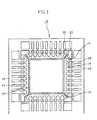
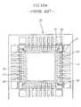
- FIG. 1is a plan view illustrating a lead frame provided with a locking lug type lead lock in accordance with a first embodiment of the present invention
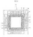
- FIG. 2is a plan view illustrating a lead frame having a disk type lead lock in accordance with a second embodiment of the present invention
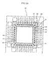
- FIGS. 3A and 3Bare plan views respectively illustrating lead frames having a dimple type lead lock in accordance with a third embodiment of the present invention.
- FIG. 3Cis a cross-sectional view partially illustrating a semiconductor package fabricated using a lead frame provided with at least one aperture, in place of the dimple, as the lead lock;
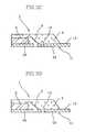
- FIG. 4is a cross-sectional view partially illustrating a semiconductor package fabricated using a lead frame having a side wall type lead lock according to a fourth embodiment of the present invention
- FIGS. 5A to 5 Dare bottom plan views respectively illustrating lead frames having an etch type lead lock according to a fifth embodiment of the present invention.
- FIG. 5Eis a cross-sectional view partially illustrating a semiconductor package fabricated using the lead frame shown in FIG. 5A;
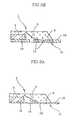
- FIGS. 6A and 6Bare cross-sectional views partially illustrating lead frames configured to have a bent-lead lead lock in accordance with a sixth embodiment of the present invention, respectively;
- FIGS. 7A to 7 Dare cross-sectional views respectively illustrating lead end grid array type semiconductor packages according to other preferred embodiments of the present invention.
- FIG. 8is an enlarged view corresponding to a portion A of FIG. 7D;
- FIG. 9is a cross-sectional view illustrating a conventional quad-flat or bi-flat semiconductor package
- FIGS. 10A and 10Bare a plan view illustrating a conventional lead frame and a cross-sectional view illustrating a bottom lead type semiconductor package fabricated using the conventional lead frame, respectively;
- FIG. 11is a cross-sectional view illustrating a conventional lead end grid array type semiconductor package.
- FIGS. 1 to 6 Billustrate lead frames respectively according to various embodiments of the present invention adapted to accomplish the primary and secondary objects of the present invention.
- All the lead frameswhich are denoted in the reference numeral 10 in FIGS. 1 to 6 B, have a basic configuration including a rectangular or square paddle 16 , a plurality of tie bars 15 for supporting the paddle 16 , and a plurality of leads 12 arranged at each of four sides or two facing sides of the paddle 16 while being spaced apart from the associated side of the paddle 16 .
- Each lead 12is provided, at its portion adjacent to the paddle 16 , with a lead lock 14 adapted to increase the bonding force of the lead 12 to a resin encapsulate 4 to be subsequently formed.
- the lead lock embodimentsprevent separation of the leads from the encapsulant resin in a lateral and/or vertical direction.
- the basic lead frame configurationalso includes dam bars 17 for supporting the leads 12 and tie bars 15 .
- the lead frames shown in FIGS. 1 to 6 Bcan be advantageously used to fabricate bottom lead type semiconductor packages in which the entire lower surface of each inner lead 12 is exposed at the bottom of the resin encapsulate 4 , as shown in FIGS. 3C, 3D, 4 , 5 E, 6 A, and 6 B, or lead end grid type semiconductor packages in which only the lower surface of the protruded end 19 protruded from the lower surface of each inner lead 12 is exposed at the bottom of the resin encapsulate 4 , as shown in FIGS. 7A to 7 D.
- FIGS. 1 to 6 Belements respectively corresponding to those in FIGS. 9 to 10 B are denoted by the same reference numerals.
- FIG. 1is a plan view illustrating a lead frame 1 which is provided with locking lug type lead lock 14 in accordance with a first embodiment of the present invention.
- the lead frame 1basically includes a paddle 16 , tie bars 15 for supporting four corners of the paddle 16 , a plurality of leads 11 arranged adjacent to each of four sides of the paddle 16 while extending perpendicularly to the associated side of the paddle 16 , and dam bars 17 for supporting the leads 11 and tie bars 15 .
- the paddle 16has a flat plate shape, as shown in FIG. 1.
- the paddle 16has a partially etched structure at its peripheral portion.
- the present inventionis not limited to such a structure of the paddle 16 .
- the paddle 16may have a rectangular or square frame structure having a central opening.
- the shape and area of the paddle and the structure of the paddle including a central opening or not including the central openingare optional.
- the present inventionis not limited by these factors.
- the tying position and number of the tie bars 15are also optional. These factors are not construed to limit the present invention.
- the lead lock 14comprises locking lugs laterally protruded from opposite side edges of each inner lead 12 at a free end of the inner lead 12 , respectively.
- each locking lughas a rectangular shape in the illustrated case, it is not limited thereto.
- the locking lugsmay have a variety of shapes such as a triangular shape or a circular shape.
- the number of locking lugsis also optional. For example, only one locking lug may be formed at one side edge of each inner lead 12 . Alternatively, a plurality of locking lugs may be formed at each side edge of each inner lead 12 .
- each inner lead 12is provided with the lead lock 14 comprising locking lugs in accordance with the embodiment of the present invention shown in FIG. 1, all leads 11 can be firmly locked in position even when they receive cutting impact during a singulation process carried out after the formation of a resin encapsulate. Accordingly, there is no possibility for the leads 11 to be separated (e.g., in a lateral direction) from the resin encapsulate 4 or for the conductive wires 3 bonded to the leads 11 to be short-circuited due to vibrations generated in the singulation process.
- each tie bar 15may have a partially etched structure at its portion arranged within a region where the paddle 16 and/or resin encapsulate is formed, in order to achieve an enhancement in the bonding strength to the semiconductor chip and/or resin encapsulate.
- each lead 11may be partially etched to have a partially etched structure at its inner end.
- Dotted lines 23 inside the dam bars 17represent singulation lines along which the lead frame 10 ′ is cut after completing a semiconductor chip mounting process, a wire bonding process, and a resin encapsulate molding process.
- the reference numeral 18denotes side rails.
- FIG. 2is a plan view illustrating a lead frame 10 having disk type lead lock 14 in accordance with a second embodiment of the present invention.
- the lead frame of the second embodimenthas the same basic configuration as that of the first embodiment, except for the shape of the lead lock 14 . Accordingly, no description will be made for the same basic configuration.
- the lead lock 14 of each inner lead 12forms a free end of the inner lead 12 by itself.
- the lead lock 14has an enlarged disk shape having a diameter larger than the width of each inner lead 12 .
- the lead lock 14may have an oval shape or a double disk shape.
- the double disk shapemay be formed to have at least two disk portions.
- such a double disk shapemay be a three or four-leafed clover shape.
- each inner lead 12is provided with the lead lock 14 having an enlarged disk structure in accordance with the embodiment of the present invention shown in FIG. 2, all leads 11 can be firmly locked in position even when they receive cutting impact during a singulation process carried out after the formation of a resin encapsulate. Accordingly, there is no possibility for the leads 11 to be separated from the resin encapsulate 4 or for the conductive wires 3 bonded to the leads 11 to be short-circuited due to vibrations generated in the singulation process. For example, lateral motion of the encapsulated lead is prevented.
- FIGS. 3A and 3Bare plan views respectively illustrating a lead frame 10 having dimple type lead lock(s) 14 in accordance with a third embodiment of the present invention.
- the lead frame of the third embodimenthas the same basic configuration as those of the first and second embodiments, except that the lead lock(s) 14 has a dimple shape. Accordingly, no description will be made for the same basic configuration.
- the lead lock 14 of each inner lead 12comprises one or two dimples formed at a free end of the inner lead 12 .
- all leads 11can be firmly locked in position even when they receive cutting impact during a singulation process carried out after the formation of a resin encapsulate. Accordingly, there is no possibility for the leads 11 to be separated from the resin encapsulate 4 or for the conductive wires 3 bonded to the leads 11 to be short-circuited due to vibrations generated in the singulation process.
- FIG. 3Aillustrates a case in which a single dimple is centrally formed at the free end of each inner lead 12 .
- FIG. 3Billustrates a case in which two dimples are formed at opposite sides of the each inner lead 12 , respectively, in such a fashion that each of them extends partially over an associated peripheral edge of the inner lead 12 and an associated side surface of the inner lead 12 .
- Such a dimple structureis not construed to limit the present invention.
- the number and position of dimplesare optional in accordance with the present invention.
- Such dimplesmay be additionally provided at each inner lead configured in accordance with the first or second embodiment. Such a configuration is optional in accordance with the present invention.
- FIG. 3Cis a cross-sectional view partially illustrating a semiconductor package 1 fabricated using a lead frame 10 having the same configuration as the lead frame of FIG. 3A.
- this semiconductor package 1includes a semiconductor chip 2 mounted on a paddle 16 of the lead frame 10 by means of an adhesive layer, leads 11 each provided at an inner end thereof with a dimple as a lead lock 14 , conductive wires 3 for electrically connecting an inner free end of an inner lead 12 included in each lead 11 to the semiconductor chip 2 , and a resin encapsulate 4 for protecting the semiconductor chip 2 and conductive wires 3 from external environments.
- the leads 11are firmly locked to the resin encapsulate 4 by virtue of the dimples each formed on the upper surface of each inner lead 12 at the inner end of the inner lead 12 .
- FIG. 3Dis a cross-sectional view partially illustrating a semiconductor package 1 fabricated using a lead frame (not shown) provided with at least one aperture, in place of the dimple, as the lead lock 14 for each lead 11 .
- the apertureserves to firmly lock the associated lead 11 to the resin encapsulate 4 . Accordingly, there is no possibility for the leads to be separated from the resin encapsulate 4 during a singulation process. For example, lateral motion of the encapsulated lead is prevented.
- FIG. 4is a cross-sectional view partially illustrating a semiconductor package 1 fabricated using a lead frame (not shown) according to a fourth embodiment of the present invention.
- each lead 11has an inverted-trapezoidal cross section in such a fashion that it has a maximum width at the top thereof and a minimum width at the bottom thereof. That is, each lead 11 has inclined side walls serving as lead lock 14 . Since each lead 11 has a taper structure increasing in width as it extends inwardly into the resin encapsulate 4 from the bottom of the resin encapsulate 4 , there is no possibility for the leads 11 to be separated from the resin encapsulate 4 even when they receive cutting impact during a singulation process.
- the semiconductor packages 1which are illustrated in FIGS. 3C to 4 respectively, have a typical structure including a semiconductor chip 2 mounted on the paddle 16 of the lead frame 10 by means of an adhesive layer, leads 11 arranged adjacent to each of four sides of the paddle 16 while extending perpendicularly to the associated side of the paddle 16 , each of the leads 11 having a lead lock 14 , conductive wires 3 for electrically connecting an inner end of each lead 11 to the semiconductor chip 2 , and a resin encapsulate 4 for encapsulating the semiconductor chip 2 and conductive wires 3 .
- each lead 11has a lower surface exposed at the bottom of the resin encapsulate 4 .
- FIGS. 5A to 5 Dare bottom plan views respectively illustrating lead frames 10 according to a fifth embodiment of the present invention.
- the lead frames 10 of the fifth embodimenthave the same basic configuration as those of the above mentioned embodiments, except that a partially etched portion extends from the inner end of each inner lead 12 as the lead lock 14 . Accordingly, no description will be made for the same basic configuration.
- FIG. 5Eis a cross-sectional view partially illustrating a semiconductor package 1 fabricated using one of the lead frames 10 respectively shown in FIGS. 5A to 5 D.
- an extensionextends inwardly from the inner end of each inner lead 12 .
- the extensionhas a partially etched structure in such a fashion that its lower surface has a higher level than that of the lower surface of the associated inner lead 12 to provide a lead separation preventing means 14 .
- the partially etched extensions of the inner leads 12 arranged adjacent to each side of the paddle 16are inclined toward the center of the paddle side in such a fashion that they have an increased inclination at positions away from the center of the paddle side, that is, toward the corners of the paddle 16 . That is, the partially etched extensions arranged adjacent to both ends of each side of the paddle 16 extend substantially in parallel to the tie bars 15 arranged adjacent thereto, respectively.
- each extensionSince the lower surface of each extension has a higher level than that of the lower surface of the associated inner lead 12 , the extension is encapsulated in a resin encapsulate 4 molded in a resin encapsulating process, as shown in FIG. 5E. Accordingly, all leads 11 can be firmly locked in position (e.g., laterally and vertically) even when they receive cutting impact during a singulation process. Accordingly, it is possible to effectively prevent the leads 11 from being separated from the resin encapsulate 4 in the singulation process.
- wingsextend laterally from opposite side edges of each inner lead 12 , respectively.
- Each winghas a partially etched structure in such a fashion that its lower surface has a higher level than that of the lower surface of the associated inner lead 12 to provide a lead lock 14 .
- No wingis provided at the side edge of each inner lead 12 arranged adjacent to an associated one of the tie bars 15 .
- wingsmay be provided at both side edges of each inner lead 12 arranged adjacent to an associated one of the tie bars 15 .
- a lug 19 bis protruded from the upper surface of each inner lead 12 at the inner end of the inner lead 12 , in addition to the wings, to provide a lead lock 14 .
- the lug 19 bcan be electrically connected directly to an associated one of pads on a semiconductor chip. Such a lug may be applied to any one of the above mentioned embodiments of the present invention or embodiments to be described hereinafter.
- Z-shaped wingsextend from opposite side edges of each inner lead 12 at the inner end of the inner lead 12 , respectively.
- Each winghas a partially etched structure in such a fashion that its lower surface has a higher level than that of the lower surface of the associated inner lead 12 to provide a lead lock 14 .
- No wingis provided at the side edge of each inner lead 12 arranged adjacent to an associated one of the tie bars 15 .
- the wingshave a Z shape, they may have other shapes.
- the lead lock 14comprises a partially etched portion extending inwardly from the inner end of each lead 12 while being buried in a resin encapsulate 4 .
- a partially etched portionmay also be provided at the intermediate portion of each lead 12 , as shown in FIG. 5E.
- the partially etched portionsare shown as being formed by partially etching the low surface of each lead 12 , they may be formed at the upper surface of each lead 12 .
- the formation of the partially etched portion at the intermediate portion of each lead 12is optional in accordance with the present invention.
- FIGS. 6A and 6Bare cross-sectional views partially illustrating lead frames 10 configured to have a bent lead lock 14 in accordance with a sixth embodiment of the present invention, respectively.
- the lead frames of the sixth embodimenthave the same basic configuration as those of the above mentioned embodiments, except that the inner end of each inner lead 12 has a bent structure to provide the lead lock 14 . Accordingly, no description will be made for the same basic configuration.
- the lead lock 14is provided by simply bending the inner end of each inner lead 12 . Accordingly, this embodiment is more effective to prevent the leads 11 from being separated from a resin encapsulate in a singulation process, as compared to the embodiments involving formation of locking lugs, wings, or dimples.
- the lead lock 14comprises the inner end of each inner lead 12 upwardly bent in perpendicular to the plane of the inner lead 12 .
- the lead lock 14comprises the inner end of each inner lead 12 bent by an angle of about 180 degrees in such a fashion that it extends in parallel to the plane of the inner lead 12 .
- the bending direction of the inner end of each inner lead 12is optional in accordance with the present invention.
- lead frames 10 and a variety of semiconductor packages 1 using those lead frames 10 in accordance with the above mentioned first through six embodiments of the present inventionhave been described, it will be appreciated that a lead frame configured in accordance with an optional combination of the above mentioned embodiments and a semiconductor package fabricated using this lead frame may also be included in the scope of the present invention.
- FIGS. 7A to 7 Dare cross-sectional views respectively illustrating lead end grid array type semiconductor packages 1 according to other embodiments of the present invention adapted to accomplish the third and fourth objects of the present invention.
- the semiconductor packages 1which are illustrated in FIGS. 7A to 7 D respectively, have a typical structure including a paddle 16 , and leads 11 arranged adjacent to each of four sides or two facing sides of the paddle 16 while extending perpendicularly to the associated side of the paddle 16 .
- Each lead 11has an inward protrusion 19 at the inner end thereof.
- the package structurealso includes a semiconductor chip 2 mounted on the paddle 16 in such a fashion that its peripheral portion is arranged on or above the inner ends of the leads 11 , an electrical insulating means 32 for preventing an electrical contact between the upper surface of each lead 11 at the inner end of the lead 11 and the lower surface of the semiconductor chip 2 at the peripheral portion of the semiconductor chip 2 , conductive wires 3 for electrically connecting the leads 11 to the semiconductor chip, respectively, a resin encapsulate 4 for encapsulating the semiconductor chip 2 and conductive wires 3 , and solder balls 5 attached to the lower surfaces of the protrusions 19 of the leads 11 arranged within a region where the resin encapsulate 4 is formed, respectively.
- the solder balls 5serve to external input/output terminals.
- the leads 11may selectively have a lead separation preventing means (not shown).
- the electrical insulating means 32comprises a double-sided adhesive polyimide tape or a typical adhesive polymer resin layer.
- the polymer resinmay be, for example, epoxy resin.
- the protrusion 19 of each lead 11is formed by partially etching the lower surface of the lead 11 at the inner end of the lead 11 and locks the lead to encapsulant 4 .
- Each protrusion 19has a lower surface serving as a solder ball land 19 a , This solder ball land 19 a is exposed at the bottom of the resin encapsulate 4 .
- the solder ball lands 19 a of the leads 11are selectively attached with solder balls 5 serving as external input/output terminals.
- a thermally-conductive adhesive layer 31is interposed between the lower surface of the semiconductor chip 2 and the upper surface of the paddle 16 .
- an insulating adhesive layer, which serves as the electrical insulator layer 32is interposed between the upper surface of each lead 11 at the inner end of the lead 11 and the lower surface of the semiconductor chip 2 at the peripheral portion of the semiconductor chip 2 .
- the phenomenon wherein the leads 11 come into contact with the lower surface of the semiconductor chip 2may occur in the case wherein the semiconductor chip 2 is bonded to the paddle 16 without keeping its accurate horizontal position, wherein a lead sweeping phenomenon causing the inner ends of the leads 11 to be raised or laterally leaned occurs during the process for injecting melted resin of high temperature and pressure to mold the resin encapsulate 4 , or wherein the inner ends of the leads 11 are deformed, due to a careless operator, in such a fashion that they are raised.
- a short circuit or electric leakagemay occur.
- the semiconductor package 1 ′′′ of FIG. 11may operate abnormally or break down.
- thermally-conductive adhesive layer 31 for bonding the semiconductor chip 2 to the paddle 16a silver-filled epoxy resin adhesive is typically used, even though the present invention is not limited thereto.
- the thermally-conductive adhesive layer 31 and/or the insulating adhesive layer 32 as the electrical insulating meansis coated in accordance with a printing or dispensing process. The coated layer is set at a high temperature after the mounting of the semiconductor chip 2 , so as to firmly bond the semiconductor chip 2 .
- a double-sided adhesive polyimide tapeis used as mentioned above, it may be attached to the inner end of each inner lead 12 .
- double-sided adhesive polyimide tapes each having a strip shapemay be used.
- each double-sided adhesive polyimide tapeis attached to the inner ends of the inner leads 12 arranged adjacent to an associated side of the paddle 16 .
- a double-sided adhesive polyimide tapeis attached to the inner ends of the inner leads 12 arranged adjacent to an associated side of the paddle 16 .
- a double-sided adhesive polyimide tape having a rectangular or square loop shapemay also be used. In this case, the tape is attached to the inner ends of all inner leads 12 arranged around the paddle 16 (FIG. 1).
- the semiconductor package 1 of FIG. 7Bhas the same basic configuration as that of FIG. 7A, except that only the insulating adhesive layer 32 made of an insulating adhesive resin such as an epoxy adhesive resin is formed on the paddle 16 without formation of the thermally-conductive adhesive layer 31 made of, for example, a silver-filled epoxy resin. Accordingly, no further description will be made.
- the semiconductor package 1 of FIG. 7Chas the same basic configuration as that of FIG. 7A. Accordingly, no description will be made for the same basic configuration.
- an insulating materialsuch as polyimide is uniformly coated over the entire lower surface of the semiconductor chip 2 using a well-known process such as a spin coating process, a duct blade process, a spraying process, a dispensing process or a printing process. The coated layer is then set at a high temperature. Practically, the insulating material is coated over a wafer (not shown) including a plurality of semiconductor chips 2 .
- a sawing processis carried out to separate the wafer into package units respectively including individual semiconductor chips 2 each coated with the insulating layer 32 over the entire lower surface thereof.
- Each semiconductor chip 2is then mounted on the paddle 16 of a lead frame having a configuration according to the present invention by means of a well-known thermally-conductive adhesive layer.
- the inner end of each lead 11is maintained not to come into direct contact with the lower surface of the semiconductor chip 2 .
- there is no problemsuch as a short circuit or electric leakage even when the semiconductor chip 2 is bonded to the paddle 16 without keeping its accurate horizontal position or when a lead sweeping phenomenon occurs during a molding process.
- the semiconductor package 1 of FIG. 7Dhas the same basic configuration as that of FIG. 7A, except that only the insulating adhesive layer 32 made of an insulating adhesive resin such as an epoxy adhesive resin is formed on the paddle 16 . Accordingly, no further description will be made.
- the semiconductor package 1which has a configuration shown in one of FIGS. 7A to 7 D, can be fabricated by mounting a semiconductor chip 2 having input/output pads (not shown) on the paddle 16 of a lead frame 10 having a plurality of leads 11 , each having an inner lead and an outer lead integral with each other, in such a fashion that the peripheral portion of the semiconductor chip 2 is arranged on or above the inner leads of the leads 11 in accordance with a fabrication method of the present invention.
- This methodincludes a semiconductor chip mounting step for mounting a semiconductor chip on the upper surface of inner leads, included in each of lead frame units of a lead frame strip, at the inner ends of the inner leads by means of a thermally-conductive insulating means 32 , a wire bonding step for electrically connecting the inner end of each inner lead to an associated one of input/output pads of the semiconductor chip via a conductive wire 3 , a resin encapsulate molding step for molding a resin encapsulate 4 adapted to encapsulate the semiconductor chip along with the conductive wires 3 and inner leads associated with the semiconductor chip while allowing each of the associated inner leads to have a portion exposed at the bottom of the resin encapsulate 4 , an optional solder ball attaching step for attaching solder balls 5 , as external input/output terminals, to the exposed portions of the inner leads, and a singulation step for cutting the outer leads of the lead frame strip around the resin encapsulates 4 at regions where the outer ends of the outer leads respectively included in adjacent ones of the lead frame units are
- FIG. 8is an enlarged view corresponding to a portion A of FIG. 7D.
- FIG. 8illustrates a cross section of a structure obtained after cleaning the solder ball lands 19 a by removing the lower portion of each protrusion 19 , exposed at the bottom of the resin encapsulate 4 in the semiconductor package 1 , to a desired depth and over a desired area, selectively plating gold and/or nickel, and/or aluminum, or an alloy thereof on the cleaned solder ball lands 19 a , and then fusing solder balls 5 , as external input/output terminals, on the plated solder ball lands 19 a.
- a lead framewhich includes a plurality of lead frame units 10 each having a paddle 16 , and a plurality of leads 11 arranged adjacent to each of four sides or two facing sides of the paddle.
- Each lead 11has an inner lead and an outer lead integral with each other.
- the inner lead of each lead 11has a protrusion 19 protruded from the lower surface of the inner lead at the inner end of the inner lead 11 .
- This methodincludes a semiconductor chip mounting step for mounting a semiconductor chip on the paddle 16 of each lead frame unit 10 , a wire bonding step for electrically connecting the mounted semiconductor chip 2 to the inner end of each inner lead 11 at the upper surface of the inner lead 11 via a conductive wire 3 , a resin encapsulate molding step for molding a resin encapsulate 4 adapted to encapsulate the semiconductor chip along with the conductive wires 3 and the inner ends of the inner leads associated with the semiconductor chip while allowing each of the protrusions 19 to have a lower surface exposed at the bottom of the resin encapsulate 4 , a marking and cleaning step for radiating a laser beam onto a surface of the resin encapsulate 4 , a marking and cleaning step for radiating a laser beam onto a surface of the resin encapsulate 4 to mark characters or signs of the surface of the resin encapsulate 4 while radiating a laser beam onto the lower surface of each protrusion 19 to remove set resin coated on the lower surface of the protrusion 19 after being flashe
- the semiconductor chip mounting stepis carried out using an adhesive layer 31 and/or an adhesive layer 32 interposed between the semiconductor chip 2 and the paddle 16 of the lead frame 10 .
- a laser beamis radiated onto a selected surface portion of the resin encapsulate 4 to indicate characters or signs representing the manufacturer or model name.
- a laser beamis radiated onto the lower surface of each protrusion 19 , thereby removing set resin coated on the lower surface of the protrusion 19 after being flashed during the resin encapsulate molding step.
- Each of the protrusions 19may have a desired irregularity shape having a desired area and a desired depth so that the protrusions 19 provide a desired pattern, such as a matrix pattern, a line patter, a dot pattern, or a line/dot pattern, having an increased surface area, thereby being capable of providing an increased fusing force of solder balls to be formed at the subsequent solder ball attaching step which may be optionally carried out.
- a plating stepmay also be conducted to plate gold and/or nickel, and/or aluminum, or an alloy thereof on the cleaned solder ball lands 19 a .
- solder balls 5 serving as external input/output terminalscan be easily and securely attached to the solder ball lands 19 a at the solder ball attaching step, respectively.
- the marking and cleaning stepis conducted using a laser beam emitted from a CO 2 laser, an Nd laser, a diode laser, or an excimer laser.
- the marking step and the cleaning stepcan be performed in a simultaneous or sequential fashion using one or more laser.
Landscapes
- Physics & Mathematics (AREA)
- Engineering & Computer Science (AREA)
- Computer Hardware Design (AREA)
- Microelectronics & Electronic Packaging (AREA)
- Power Engineering (AREA)
- Condensed Matter Physics & Semiconductors (AREA)
- General Physics & Mathematics (AREA)
- Geometry (AREA)
- Lead Frames For Integrated Circuits (AREA)
- Structures Or Materials For Encapsulating Or Coating Semiconductor Devices Or Solid State Devices (AREA)
Abstract
Description
- 1. Field of the Invention[0001]
- The present invention relates to a lead frame with lead separation preventing means, a semiconductor package using the lead frame, and a method for fabricating the semiconductor package. More particularly, the present invention relates to a lead frame having a lead separation preventing means provided at a free end of each inner lead and adapted to increase a bonding force of the inner lead to a resin encapsulate encapsulating the lead frame to fabricate a semiconductor package, thereby effectively preventing a separation of the inner lead from occurring in a singulation process involved in the fabrication of the semiconductor package. The present invention also relates to the semiconductor package fabricated using the lead frame, and a fabrication method for the semiconductor package.[0002]
- 2. Description of the Related Art[0003]
- In pace with the recent trend of electronic appliances, such as electronic products for domestic and official purposes, communication appliances, and computers, toward a compactness and high performance, semiconductor packages, which are used for such electronic appliances, have been required to have a compact, highly multi-pinned, light, simple structure.[0004]
- Such a requirement for semiconductor packages has resulted in developments of semiconductor packages having a structure in which the lower surface of each lead is exposed at the bottom of the resin encapsulate. For such semiconductor packages, there are bottom lead type semiconductor packages and lead end grid array type semiconductor packages. Currently, the demand of semiconductor packages having such a structure is being increased.[0005]
- Similarly to typical quad-flat or bi-flat type semiconductor packages, such bottom lead type or lead end grid array type semiconductor packages can be fabricated using a well-known method. This method may involve a sawing step for cutting a wafer formed with a plurality of semiconductor chip units into pieces respectively corresponding to those semiconductor chip units, thereby separating the semiconductor chip units from one another, a semiconductor chip mounting step for mounting the semiconductor chip units on respective paddles of lead frame units integrally formed on a lead frame strip by means of a thermally-conductive adhesive resin, a wire bonding step for electrically connecting a free end of each inner lead, included in each lead frame unit, to an associated one of input/output terminals of the semiconductor chip unit mounted on the lead frame unit, a resin encapsulate molding step for molding a resin encapsulate adapted to encapsulate each semiconductor chip unit and a bonding region including bonding wires for the semiconductor chip unit, using encapsulating resin, for the protection of those elements from external environments, thereby forming semiconductor packages each including one semiconductor chip unit and one lead frame unit, a singulation step for cutting inner portions of dam bars of each lead frame unit, thereby separating the semiconductor packages from one another, and a marking step for marking characters or signs on the surface of the resin encapsulate included in each semiconductor package. In the fabrication of quad-flat or bi-flat semiconductor packages, a lead forming step is involved to form leads outwardly protruded by a considerable length from a resin encapsulate into a particular terminal shape, for example, a “J” shape. In the fabrication of bottom lead type or lead end grid array type semiconductor packages, however, it is typically unnecessary to use such a lead forming step. In bottom lead type or lead end grid array type semiconductor packages, the lower surface or free end of each lead is exposed at the bottom of the resin encapsulate. Accordingly, the exposed portion of each lead may be directly used as an external input/output terminal or attached with a solder ball to be used as an external input/output terminal.[0006]
- A typical structure of such quad-flat or bi-flat semiconductor packages is illustrated in a cross-sectional view of FIG. 9. Now, this structure will be described in brief in conjunction with FIG. 9. In FIG. 9, the[0007]
reference numeral 1′ denotes a semiconductor package having a quad-flat or bi-flat structure. As shown in FIG. 9, this semiconductor package includes asemiconductor chip 2 bonded to apaddle 16 by means of a thermally-conductive epoxy resin 32, and a plurality ofleads 11 arranged at each of four sides or two facing sides of thepaddle 16 in such fashion that they are spaced apart from the associated side of thepaddle 16 while extending perpendicularly to the associated side of thepaddle 16. The semiconductor package also includes a plurality ofconductive wires 3 for electrically connecting theinner leads 12 to thesemiconductor chip 2, respectively, and aresin encapsulate 4 for encapsulating thesemiconductor chip 2 andconductive wires 3. The semiconductor package further includesouter leads 13 extending outwardly from theinner pads 12, respectively. Eachouter lead 13 has a particular shape, for example, a “J” shape, so that it is used as an input/output terminal in a state in which the semiconductor package is mounted on a mother board. - FIGS. 10A and 10B are, respectively, a plan view illustrating a conventional lead frame and a cross-sectional view illustrating a bottom lead type semiconductor package fabricated using the lead frame, respectively.[0008]
- As shown in FIG. 10A, the lead frame, which is denoted by the[0009]
reference numeral 10′, includes apaddle 16,tie bars 15 for supporting respective corners of thepaddle 16, a plurality ofleads 11 arranged at each of four sides of thepaddle 16 in such a fashion that they extend perpendicularly to the associated side of thepaddle 16, anddam bars 17 for supporting theleads 11 andtie bars 15. Eachlead 11 has aninner lead 12 encapsulated by a resin encapsulate (shown byphantom lines 21 in FIG. 10A) to be subsequently formed, and anouter lead 13 extending outwardly from the resin encapsulate. Dottedlines 23 inside thedam bars 17 represent singulation lines along which thelead frame 10′ is cut after completing a semiconductor chip mounting process, a wire bonding process, and a resin encapsulate molding process. In FIG. 10A, thereference numeral 18 denotes side rails. - The bottom lead type semiconductor package denoted by the[0010]
reference numeral 1″ in FIG. 10B is that fabricated using the lead frame of FIG. 10A. As shown in FIG. 10B, thesemiconductor package 1″ includes asemiconductor chip 2 bonded to thepaddle 16 of thelead frame 10′, along with theleads 11 of thelead frame 10′. As mentioned above, theleads 11 are arranged at each of four sides of thepaddle 16 while being spaced apart from the associated side of thepaddle 16 by a desired distance. Thesemiconductor package 1″ also includesconductive wires 3 for electrically connecting the inner leads to thesemiconductor chip 2, and aresin encapsulate 4 for encapsulating thesemiconductor chip 2 andconductive wires 3. Theouter lead 13 of eachlead 11 has a length shorter than that of a typical quad-flat semiconductor package. Typically, the outer lead of eachlead 11 is not subjected to any forming process. The lower surface of eachinner lead 12 is exposed at the bottom of theresin encapsulate 4, so that it serves as an external input/output terminal, along with the lower surface of the associatedouter lead 13. - In the above mentioned bottom lead[0011]
type semiconductor package 1″, however, theinner leads 12, which are encapsulated in theresin encapsulate 4 in such a fashion that their lower surfaces are exposed, have a planar structure having a simple rectangular shape or an end-rounded rectangular shape. By virtue of such a planar structure of theinner leads 12, there is a high possibility for theleads 11 to be separated from theresin encapsulate 4 due to cutting impact applied thereto in a singulation process for cutting them inside thedam bars 17 or for theconductive wires 3 bonded to theleads 12 to be short-circuited due to vibrations generated in the singulation process. This problem becomes more severe in the case of a compact and highly multi-pinned package structure having an increased number of leads because the increased number of leads results in a reduction in the width of each lead, thereby reducing the area of each lead contacting the resin encapsulate. - In an operation of the semiconductor chip, problems similar to those occurring in the singulation process may occur. For example, the bonding force between the leads and the[0012]
resin encapsulate 4 may be degraded due to a considerable thermal expansion difference among thepaddle 16, leads11,conductive wires 3 andresin encapsulate 4. Due to the same reason, theconductive wires 3 may be shorted-circuited. - FIG. 11 is a cross-sectional view illustrating a conventional lead end grid array type semiconductor package. This lead end grid array type semiconductor package has the same basic structure as that of the bottom lead type semiconductor package shown in FIG. 10B. Accordingly, the lead end grid array type semiconductor package of FIG. 11 will be described only in conjunction with its differences from FIG. 10B.[0013]
- The semiconductor package of FIG. 11, which is denoted by the[0014]
reference numeral 1′″, has leads11 formed in accordance with a half etch process to haveprotrusions 19, respectively. Theprotrusion 19 of eachlead 11 has a lower surface exposed at the bottom of theresin encapsulate 4. In order to allow thesemiconductor package 1′″ to have a light, thin, simple and compact structure, the peripheral portion of thesemiconductor chip 2 extends beyond the peripheral edge of thepaddle 16 to a region, where the inner ends of theleads 11 are positioned. That is, the peripheral portion of thesemiconductor chip 2 is positioned above the inner ends of theleads 11. Theprotrusion 19 of eachlead 11 is attached at its lower surface with asolder ball 5 serving as an external input/output terminal. In the above mentioned conventional lead end grid arraytype semiconductor package 1′″, however, the inner ends of theleads 11 may come into contact with the lower surfaces of thesemiconductor chip 2 in the case where thesemiconductor chip 2 is bonded to thepaddle 16 without keeping its accurate horizontal position, where the inner ends of theleads 11 are raised or laterally leaned during the process for injecting melted resin of high temperature and pressure to mold theresin encapsulate 4, or where the inner ends of theleads 11 are deformed, due to a careless operator, in such a fashion that they are raised. When the inner ends of theleads 11 come into contact with the lower surface of thesemiconductor chip 2, a short circuit or electric leakage may occur. As a result, thesemiconductor package 1′″ may operate abnormally or break down. - In the fabrication of the above mentioned conventional lead end grid array[0015]
type semiconductor package 1′″, there is also a possibility for theprotrusions 19 of theleads 11 to be partially or completely coated with the encapsulating resin at their lower surfaces due to a flash phenomenon which may occur in the resin molding process. The flash phenomenon is a phenomenon wherein the melted encapsulating resin spreads through gaps defined by the leads and a mold used. In such a case, it is impossible to securely attachsolder balls 5 to theprotrusions 19 of the leads11. Although the attachment ofsolder balls 5 is achieved, thesesolder balls 5 may be easily detached. Furthermore, the attachedsolder balls 5 exhibit a degraded conduction quality. Consequently, there is a high possibility for thesolder balls 5 to lose their function as external terminals. - In order to solve this problem, conventional semiconductor package fabricating methods involve a process for removing set resin film partially or completely coated over the lower surface of each[0016]
protrusion 19, that is, asolder ball land 19a, after the completion of the molding process. Conventionally, this process is carried out using a chemical treating method using a strong acid such as sulfuric acid or hydrochloric acid or a mechanical treating method using metal bead impact or water jet. However, the chemical treating method involves problems of environmental pollution and requirement of purification. On the other hand, the mechanical treating method involves formation of cracks in theresin encapsulate 4, generation and accumulation of static electricity, and existence of residual flashed resin in a set state. - Therefore, a primary object of the invention is to provide a lead frame provided with a lead lock adapted to increase the bonding force of inner leads to a resin encapsulate, thereby being capable of effectively preventing a separation of the leads from the resin encapsulate upon cutting the leads for a singulation of bottom lead type semiconductor packages. The embodiments of lead locks described herein prevent the leads from being separated from the encapsulate in a lateral direction parallel to the length of the lead and/or a vertical direction perpendicular to the length of the lead.[0017]
- A secondary object of the invention is to provide a semiconductor package fabricated using the lead frame capable of accomplishing the primary object of the invention.[0018]
- A third object of the invention is to provide a lead end grid array type semiconductor package having an insulating structure capable of preventing the inner ends of leads from coming, at their upper surfaces, into contact with the lower surface of an associated semiconductor chip.[0019]
- A fourth object of the invention is to provide a method for fabricating the semiconductor package capable of accomplishing the third object of the invention.[0020]
- A fifth object of the invention is to provide a method for fabricating a lead end grid array semiconductor package, which method is capable of safely and surely removing set resin coated on solder ball lands after being flashed, without causing generation of static electricity, formation of cracks, environmental pollution, and requirement of any separate machine.[0021]
- In accordance with one aspect, the present invention provides a lead frame for a bottom lead type or lead end grid type semiconductor package comprising: a rectangular or square paddle for mounting a semiconductor chip thereon; a plurality of tie bars for supporting the paddle; a plurality of leads arranged at each of four sides or two facing sides of the paddle in such a fashion that they are spaced apart from the associated side of the paddle while extending perpendicularly to the associated side of the paddle, each of the leads having one or more lead locks adapted to increase a bonding force of the lead to a resin encapsulate subsequently molded to encapsulate the lead frame for fabrication of the semiconductor package; and dam bars for supporting the leads and the tie bars.[0022]
- In accordance with another aspect, the present invention provides a semiconductor package comprising: a paddle; a semiconductor chip mounted on the paddle by an adhesive layer interposed between the paddle and the semiconductor chip; a plurality of leads arranged at each of four sides or two facing sides of the paddle in such a fashion that they are spaced apart from the associated side of the paddle while extending perpendicularly to the associated side of the paddle, each of the leads having one or more lead locks; conductive wires for electrically connecting respective inner ends of the leads to the semiconductor chip; a resin encapsulate for encapsulating the semiconductor chip and the conductive wires; and each of the leads having a lower surface exposed at the bottom of the resin encapsulate within a region where the resin encapsulate is arranged.[0023]
- In accordance with another aspect, the present invention provides a semiconductor package comprising: a paddle, a plurality of leads arranged at each of four sides or two facing sides of the paddle in such a fashion that they are spaced apart from the associated side of the paddle while extending perpendicularly to the associated side of the paddle, each of the leads having a protrude at a lower surface thereof; a semiconductor chip mounted on the paddle in such a fashion that a peripheral portion thereof is arranged over an inner end of each of the leads; an electrical insulator for preventing the leads from coming into electrical contact with the semiconductor chip; conductive wires for electrically connecting respective inner ends of the leads to the semiconductor chip; and a resin encapsulate for encapsulating the semiconductor chip and the conductive wires.[0024]
- In accordance with another aspect, the present invention provides a method for fabricating semiconductor packages by mounting semiconductor chips each having input/output pads on paddles of lead frame units included in a lead frame strip, each of the lead frame units having a plurality of leads each having an inner lead and an outer lead integral with each other, each of the semiconductor chip being arranged over the inner leads of the leads associated therewith at a peripheral portion thereof, comprising: a semiconductor chip mounting step for mounting each of the semiconductor chips on at least the upper surfaces of the inner leads associated therewith by thermally-conductive insulator; a wire bonding step for electrically connecting an inner end of each inner lead to an associated one of input/output pads of the semiconductor chip via a conductive wire; a resin encapsulate molding step for molding a resin encapsulate adapted to encapsulate the semiconductor chip along with the conductive wires and the inner leads associated with the semiconductor chip while allowing each of the associated inner leads to have a portion exposed at the bottom of the resin encapsulate; and a singulation step for cutting the outer leads of the lead frame strip around the resin encapsulates at regions where outer ends of the outer leads respectively included in adjacent ones of the lead frame units are connected to each other.[0025]
- In accordance with another aspect, the present invention provides a method for fabricating semiconductor packages comprising: a lead frame preparing step for preparing a lead frame strip including a plurality of lead frame units each having a paddle, and a plurality of leads each having an inner lead and an outer lead integral with each other, the inner lead having a protrusion protruded from a lower surface of the inner lead at an inner end of the inner lead; a semiconductor chip mounting step for mounting a semiconductor chip on the paddle of each of the lead frame units; a wire bonding step for electrically connecting the mounted semiconductor chip to the inner end of each of the inner leads at an upper surface of the inner lead via a conductive wire; a resin encapsulate molding step for molding a resin encapsulate adapted to encapsulate the semiconductor chip along with the conductive wires and the inner ends of the inner leads associated with the semiconductor chip while allowing each of the protrusions to have a lower surface exposed at the bottom of the resin encapsulate; a marking and cleaning step for radiating a laser beam onto a surface of the resin encapsulate to mark characters or signs on the surface of the resin encapsulate while radiating a laser beam onto the lower surface of each of the protrusions to remove set resin coated on the lower surface of the protrusion after being flashed during the resin encapsulate molding step; and a singulation step for cutting the outer leads of the lead frame strip around the resin encapsulates at regions where the outer ends of the outer leads respectively included in adjacent ones of the lead frame units are connected to each other.[0026]
- Other objects and aspects of the invention will become apparent from the following description of embodiments with reference to the accompanying drawings in which:[0027]
- FIG. 1 is a plan view illustrating a lead frame provided with a locking lug type lead lock in accordance with a first embodiment of the present invention;[0028]
- FIG. 2 is a plan view illustrating a lead frame having a disk type lead lock in accordance with a second embodiment of the present invention;[0029]
- FIGS. 3A and 3B are plan views respectively illustrating lead frames having a dimple type lead lock in accordance with a third embodiment of the present invention;[0030]
- FIG. 3C is a cross-sectional view partially illustrating a semiconductor package fabricated using a lead frame provided with at least one aperture, in place of the dimple, as the lead lock;[0031]
- FIG. 4 is a cross-sectional view partially illustrating a semiconductor package fabricated using a lead frame having a side wall type lead lock according to a fourth embodiment of the present invention;[0032]
- FIGS. 5A to[0033]5D are bottom plan views respectively illustrating lead frames having an etch type lead lock according to a fifth embodiment of the present invention;
- FIG. 5E is a cross-sectional view partially illustrating a semiconductor package fabricated using the lead frame shown in FIG. 5A;[0034]
- FIGS. 6A and 6B are cross-sectional views partially illustrating lead frames configured to have a bent-lead lead lock in accordance with a sixth embodiment of the present invention, respectively;[0035]
- FIGS. 7A to[0036]7D are cross-sectional views respectively illustrating lead end grid array type semiconductor packages according to other preferred embodiments of the present invention;
- FIG. 8 is an enlarged view corresponding to a portion A of FIG. 7D;[0037]
- FIG. 9 is a cross-sectional view illustrating a conventional quad-flat or bi-flat semiconductor package;[0038]
- FIGS. 10A and 10B are a plan view illustrating a conventional lead frame and a cross-sectional view illustrating a bottom lead type semiconductor package fabricated using the conventional lead frame, respectively; and[0039]
- FIG. 11 is a cross-sectional view illustrating a conventional lead end grid array type semiconductor package.[0040]
- FIGS.[0041]1 to6B illustrate lead frames respectively according to various embodiments of the present invention adapted to accomplish the primary and secondary objects of the present invention. All the lead frames, which are denoted in the
reference numeral 10 in FIGS.1 to6B, have a basic configuration including a rectangular orsquare paddle 16, a plurality of tie bars15 for supporting thepaddle 16, and a plurality ofleads 12 arranged at each of four sides or two facing sides of thepaddle 16 while being spaced apart from the associated side of thepaddle 16. Eachlead 12 is provided, at its portion adjacent to thepaddle 16, with alead lock 14 adapted to increase the bonding force of thelead 12 to aresin encapsulate 4 to be subsequently formed. The lead lock embodiments prevent separation of the leads from the encapsulant resin in a lateral and/or vertical direction. The basic lead frame configuration also includes dam bars17 for supporting theleads 12 and tie bars15. - The lead frames shown in FIGS.[0042]1 to6B can be advantageously used to fabricate bottom lead type semiconductor packages in which the entire lower surface of each
inner lead 12 is exposed at the bottom of theresin encapsulate 4, as shown in FIGS. 3C, 3D,4,5E,6A, and6B, or lead end grid type semiconductor packages in which only the lower surface of theprotruded end 19 protruded from the lower surface of eachinner lead 12 is exposed at the bottom of theresin encapsulate 4, as shown in FIGS. 7A to7D. - Now, the lead frames adapted to accomplish the primary and secondary objects of the present invention will be described in conjunction with FIGS.[0043]1 to6B, respectively. In FIGS.1 to6B, elements respectively corresponding to those in FIGS.9 to10B are denoted by the same reference numerals.
- FIG. 1 is a plan view illustrating a[0044]
lead frame 1 which is provided with locking lugtype lead lock 14 in accordance with a first embodiment of the present invention. As shown in FIG. 1, thelead frame 1 basically includes apaddle 16, tie bars15 for supporting four corners of thepaddle 16, a plurality ofleads 11 arranged adjacent to each of four sides of thepaddle 16 while extending perpendicularly to the associated side of thepaddle 16, and dam bars17 for supporting theleads 11 and tie bars15. - The[0045]
paddle 16 has a flat plate shape, as shown in FIG. 1. In order to increase the bonding force to the resin encapsulate (not shown), thepaddle 16 has a partially etched structure at its peripheral portion. However, the present invention is not limited to such a structure of thepaddle 16. In accordance with the present invention, thepaddle 16 may have a rectangular or square frame structure having a central opening. The shape and area of the paddle and the structure of the paddle including a central opening or not including the central opening are optional. The present invention is not limited by these factors. In accordance with the present invention, the tying position and number of the tie bars15 are also optional. These factors are not construed to limit the present invention. - In accordance with the embodiment of the present invention illustrated in FIG. 1, the[0046]
lead lock 14 comprises locking lugs laterally protruded from opposite side edges of eachinner lead 12 at a free end of theinner lead 12, respectively. Although each locking lug has a rectangular shape in the illustrated case, it is not limited thereto. The locking lugs may have a variety of shapes such as a triangular shape or a circular shape. The number of locking lugs is also optional. For example, only one locking lug may be formed at one side edge of eachinner lead 12. Alternatively, a plurality of locking lugs may be formed at each side edge of eachinner lead 12. - Since each[0047]
inner lead 12 is provided with thelead lock 14 comprising locking lugs in accordance with the embodiment of the present invention shown in FIG. 1, all leads11 can be firmly locked in position even when they receive cutting impact during a singulation process carried out after the formation of a resin encapsulate. Accordingly, there is no possibility for theleads 11 to be separated (e.g., in a lateral direction) from the resin encapsulate4 or for theconductive wires 3 bonded to theleads 11 to be short-circuited due to vibrations generated in the singulation process. - Alternatively, each[0048]
tie bar 15 may have a partially etched structure at its portion arranged within a region where thepaddle 16 and/or resin encapsulate is formed, in order to achieve an enhancement in the bonding strength to the semiconductor chip and/or resin encapsulate. For the same purpose, each lead11 may be partially etched to have a partially etched structure at its inner end. - Dotted[0049]
lines 23 inside the dam bars17 represent singulation lines along which thelead frame 10′ is cut after completing a semiconductor chip mounting process, a wire bonding process, and a resin encapsulate molding process. In FIG. 10A, thereference numeral 18 denotes side rails. - FIG. 2 is a plan view illustrating a[0050]
lead frame 10 having disktype lead lock 14 in accordance with a second embodiment of the present invention. The lead frame of the second embodiment has the same basic configuration as that of the first embodiment, except for the shape of thelead lock 14. Accordingly, no description will be made for the same basic configuration. - In accordance with the second embodiment of the present invention, the[0051]
lead lock 14 of eachinner lead 12 forms a free end of theinner lead 12 by itself. As shown in FIG. 2, thelead lock 14 has an enlarged disk shape having a diameter larger than the width of eachinner lead 12. Of course, this shape is not construed to limit the present invention. Thelead lock 14 may have an oval shape or a double disk shape. The double disk shape may be formed to have at least two disk portions. For example, such a double disk shape may be a three or four-leafed clover shape. - Since each[0052]
inner lead 12 is provided with thelead lock 14 having an enlarged disk structure in accordance with the embodiment of the present invention shown in FIG. 2, all leads11 can be firmly locked in position even when they receive cutting impact during a singulation process carried out after the formation of a resin encapsulate. Accordingly, there is no possibility for theleads 11 to be separated from the resin encapsulate4 or for theconductive wires 3 bonded to theleads 11 to be short-circuited due to vibrations generated in the singulation process. For example, lateral motion of the encapsulated lead is prevented. - FIGS. 3A and 3B are plan views respectively illustrating a[0053]
lead frame 10 having dimple type lead lock(s)14 in accordance with a third embodiment of the present invention. The lead frame of the third embodiment has the same basic configuration as those of the first and second embodiments, except that the lead lock(s)14 has a dimple shape. Accordingly, no description will be made for the same basic configuration. - In accordance with the third embodiment of the present invention illustrated in FIGS. 3A and 3B, the[0054]
lead lock 14 of eachinner lead 12 comprises one or two dimples formed at a free end of theinner lead 12. By virtue of such dimples, all leads11 can be firmly locked in position even when they receive cutting impact during a singulation process carried out after the formation of a resin encapsulate. Accordingly, there is no possibility for theleads 11 to be separated from the resin encapsulate4 or for theconductive wires 3 bonded to theleads 11 to be short-circuited due to vibrations generated in the singulation process. - FIG. 3A illustrates a case in which a single dimple is centrally formed at the free end of each[0055]
inner lead 12. On the other hand, FIG. 3B illustrates a case in which two dimples are formed at opposite sides of the eachinner lead 12, respectively, in such a fashion that each of them extends partially over an associated peripheral edge of theinner lead 12 and an associated side surface of theinner lead 12. Such a dimple structure is not construed to limit the present invention. The number and position of dimples are optional in accordance with the present invention. Such dimples may be additionally provided at each inner lead configured in accordance with the first or second embodiment. Such a configuration is optional in accordance with the present invention. - FIG. 3C is a cross-sectional view partially illustrating a[0056]
semiconductor package 1 fabricated using alead frame 10 having the same configuration as the lead frame of FIG. 3A. As shown in FIG. 3C, thissemiconductor package 1 includes asemiconductor chip 2 mounted on apaddle 16 of thelead frame 10 by means of an adhesive layer, leads11 each provided at an inner end thereof with a dimple as alead lock 14,conductive wires 3 for electrically connecting an inner free end of aninner lead 12 included in each lead11 to thesemiconductor chip 2, and aresin encapsulate 4 for protecting thesemiconductor chip 2 andconductive wires 3 from external environments. In thissemiconductor package 1, theleads 11 are firmly locked to the resin encapsulate4 by virtue of the dimples each formed on the upper surface of eachinner lead 12 at the inner end of theinner lead 12. - FIG. 3D is a cross-sectional view partially illustrating a[0057]
semiconductor package 1 fabricated using a lead frame (not shown) provided with at least one aperture, in place of the dimple, as thelead lock 14 for each lead11. In this case, the aperture serves to firmly lock the associatedlead 11 to theresin encapsulate 4. Accordingly, there is no possibility for the leads to be separated from the resin encapsulate4 during a singulation process. For example, lateral motion of the encapsulated lead is prevented. - FIG. 4 is a cross-sectional view partially illustrating a[0058]
semiconductor package 1 fabricated using a lead frame (not shown) according to a fourth embodiment of the present invention. In accordance with the fourth embodiment, each lead11 has an inverted-trapezoidal cross section in such a fashion that it has a maximum width at the top thereof and a minimum width at the bottom thereof. That is, each lead11 has inclined side walls serving aslead lock 14. Since each lead11 has a taper structure increasing in width as it extends inwardly into the resin encapsulate4 from the bottom of theresin encapsulate 4, there is no possibility for theleads 11 to be separated from the resin encapsulate4 even when they receive cutting impact during a singulation process. - The semiconductor packages[0059]1, which are illustrated in FIGS. 3C to4 respectively, have a typical structure including a
semiconductor chip 2 mounted on thepaddle 16 of thelead frame 10 by means of an adhesive layer, leads11 arranged adjacent to each of four sides of thepaddle 16 while extending perpendicularly to the associated side of thepaddle 16, each of theleads 11 having alead lock 14,conductive wires 3 for electrically connecting an inner end of each lead11 to thesemiconductor chip 2, and aresin encapsulate 4 for encapsulating thesemiconductor chip 2 andconductive wires 3. In this package structure, each lead11 has a lower surface exposed at the bottom of theresin encapsulate 4. - FIGS. 5A to[0060]5D are bottom plan views respectively illustrating lead frames10 according to a fifth embodiment of the present invention. The lead frames10 of the fifth embodiment have the same basic configuration as those of the above mentioned embodiments, except that a partially etched portion extends from the inner end of each
inner lead 12 as thelead lock 14. Accordingly, no description will be made for the same basic configuration. FIG. 5E is a cross-sectional view partially illustrating asemiconductor package 1 fabricated using one of the lead frames10 respectively shown in FIGS. 5A to5D. - In the case of FIG. 5A, an extension extends inwardly from the inner end of each[0061]
inner lead 12. The extension has a partially etched structure in such a fashion that its lower surface has a higher level than that of the lower surface of the associatedinner lead 12 to provide a leadseparation preventing means 14. The partially etched extensions of the inner leads12 arranged adjacent to each side of thepaddle 16 are inclined toward the center of the paddle side in such a fashion that they have an increased inclination at positions away from the center of the paddle side, that is, toward the corners of thepaddle 16. That is, the partially etched extensions arranged adjacent to both ends of each side of thepaddle 16 extend substantially in parallel to the tie bars15 arranged adjacent thereto, respectively. Since the lower surface of each extension has a higher level than that of the lower surface of the associatedinner lead 12, the extension is encapsulated in aresin encapsulate 4 molded in a resin encapsulating process, as shown in FIG. 5E. Accordingly, all leads11 can be firmly locked in position (e.g., laterally and vertically) even when they receive cutting impact during a singulation process. Accordingly, it is possible to effectively prevent theleads 11 from being separated from the resin encapsulate4 in the singulation process. - In the case of FIG. 5B, wings extend laterally from opposite side edges of each[0062]
inner lead 12, respectively. Each wing has a partially etched structure in such a fashion that its lower surface has a higher level than that of the lower surface of the associatedinner lead 12 to provide alead lock 14. No wing is provided at the side edge of eachinner lead 12 arranged adjacent to an associated one of the tie bars15. However, this is not construed to limit the present invention. In accordance with the present invention, wings may be provided at both side edges of eachinner lead 12 arranged adjacent to an associated one of the tie bars15. - In the case of FIG. 5C, a[0063]
lug 19bis protruded from the upper surface of eachinner lead 12 at the inner end of theinner lead 12, in addition to the wings, to provide alead lock 14. Thelug 19bcan be electrically connected directly to an associated one of pads on a semiconductor chip. Such a lug may be applied to any one of the above mentioned embodiments of the present invention or embodiments to be described hereinafter. - In the case of FIG. 5D, Z-shaped wings extend from opposite side edges of each[0064]
inner lead 12 at the inner end of theinner lead 12, respectively. Each wing has a partially etched structure in such a fashion that its lower surface has a higher level than that of the lower surface of the associatedinner lead 12 to provide alead lock 14. No wing is provided at the side edge of eachinner lead 12 arranged adjacent to an associated one of the tie bars15. However, this is not construed to limit the present invention. Also, although the wings have a Z shape, they may have other shapes. - Referring to FIG. 5E, it can be found that the[0065]
lead lock 14 comprises a partially etched portion extending inwardly from the inner end of each lead12 while being buried in aresin encapsulate 4. Such a partially etched portion may also be provided at the intermediate portion of each lead12, as shown in FIG. 5E. Although the partially etched portions are shown as being formed by partially etching the low surface of each lead12, they may be formed at the upper surface of each lead12. The formation of the partially etched portion at the intermediate portion of each lead12 is optional in accordance with the present invention. - FIGS. 6A and 6B are cross-sectional views partially illustrating lead frames[0066]10 configured to have a
bent lead lock 14 in accordance with a sixth embodiment of the present invention, respectively. The lead frames of the sixth embodiment have the same basic configuration as those of the above mentioned embodiments, except that the inner end of eachinner lead 12 has a bent structure to provide thelead lock 14. Accordingly, no description will be made for the same basic configuration. - In accordance with the sixth embodiment of the present invention, the[0067]
lead lock 14 is provided by simply bending the inner end of eachinner lead 12. Accordingly, this embodiment is more effective to prevent theleads 11 from being separated from a resin encapsulate in a singulation process, as compared to the embodiments involving formation of locking lugs, wings, or dimples. In the case of FIG. 6A, thelead lock 14 comprises the inner end of eachinner lead 12 upwardly bent in perpendicular to the plane of theinner lead 12. In the case of FIG. 6B, thelead lock 14 comprises the inner end of eachinner lead 12 bent by an angle of about180 degrees in such a fashion that it extends in parallel to the plane of theinner lead 12. The bending direction of the inner end of eachinner lead 12 is optional in accordance with the present invention. - Although a variety of lead frames[0068]10 and a variety of
semiconductor packages 1 using thoselead frames 10 in accordance with the above mentioned first through six embodiments of the present invention have been described, it will be appreciated that a lead frame configured in accordance with an optional combination of the above mentioned embodiments and a semiconductor package fabricated using this lead frame may also be included in the scope of the present invention. - FIGS. 7A to[0069]7D are cross-sectional views respectively illustrating lead end grid array
type semiconductor packages 1 according to other embodiments of the present invention adapted to accomplish the third and fourth objects of the present invention. - The semiconductor packages[0070]1, which are illustrated in FIGS. 7A to7D respectively, have a typical structure including a
paddle 16, and leads11 arranged adjacent to each of four sides or two facing sides of thepaddle 16 while extending perpendicularly to the associated side of thepaddle 16. Eachlead 11 has aninward protrusion 19 at the inner end thereof. The package structure also includes asemiconductor chip 2 mounted on thepaddle 16 in such a fashion that its peripheral portion is arranged on or above the inner ends of theleads 11, an electrical insulatingmeans 32 for preventing an electrical contact between the upper surface of each lead11 at the inner end of thelead 11 and the lower surface of thesemiconductor chip 2 at the peripheral portion of thesemiconductor chip 2,conductive wires 3 for electrically connecting theleads 11 to the semiconductor chip, respectively, aresin encapsulate 4 for encapsulating thesemiconductor chip 2 andconductive wires 3, andsolder balls 5 attached to the lower surfaces of theprotrusions 19 of theleads 11 arranged within a region where the resin encapsulate4 is formed, respectively. Thesolder balls 5 serve to external input/output terminals. - In the case of FIG. 7A, the[0071]
leads 11 may selectively have a lead separation preventing means (not shown). In accordance with the embodiment illustrated in FIG. 7A, the electrical insulatingmeans 32 comprises a double-sided adhesive polyimide tape or a typical adhesive polymer resin layer. The polymer resin may be, for example, epoxy resin. Theprotrusion 19 of each lead11 is formed by partially etching the lower surface of thelead 11 at the inner end of thelead 11 and locks the lead toencapsulant 4. Eachprotrusion 19 has a lower surface serving as asolder ball land 19a, Thissolder ball land 19ais exposed at the bottom of theresin encapsulate 4. The solder ball lands19aof theleads 11 are selectively attached withsolder balls 5 serving as external input/output terminals. - In the[0072]
semiconductor package 1 illustrated in FIG. 7A, a thermally-conductive adhesive layer 31 is interposed between the lower surface of thesemiconductor chip 2 and the upper surface of thepaddle 16. Also, an insulating adhesive layer, which serves as theelectrical insulator layer 32, is interposed between the upper surface of each lead11 at the inner end of thelead 11 and the lower surface of thesemiconductor chip 2 at the peripheral portion of thesemiconductor chip 2. - Accordingly, it is possible to effectively eliminate a short circuit occurring when the leads come into contact with the lower surface of the[0073]
semiconductor chip 2 at its upper surface. Also, all leads11 can be firmly locked in position even when they receive cutting impact during a singulation process carried out after the formation of theresin encapsulate 4. Accordingly, there is no possibility for theleads 11 to be separated from the resin encapsulate4 or for theconductive wires 3 bonded to theleads 11 to be short-circuited due to heat or vibrations. - The phenomenon wherein the[0074]
leads 11 come into contact with the lower surface of thesemiconductor chip 2 may occur in the case wherein thesemiconductor chip 2 is bonded to thepaddle 16 without keeping its accurate horizontal position, wherein a lead sweeping phenomenon causing the inner ends of theleads 11 to be raised or laterally leaned occurs during the process for injecting melted resin of high temperature and pressure to mold theresin encapsulate 4, or wherein the inner ends of theleads 11 are deformed, due to a careless operator, in such a fashion that they are raised. When the leads11 come into contact with the lower surface of thesemiconductor chip 2, as mentioned above, a short circuit or electric leakage may occur. As a result, thesemiconductor package 1′″ of FIG. 11 may operate abnormally or break down. - For the thermally-[0075]
conductive adhesive layer 31 for bonding thesemiconductor chip 2 to thepaddle 16, a silver-filled epoxy resin adhesive is typically used, even though the present invention is not limited thereto. The thermally-conductive adhesive layer 31 and/or the insulatingadhesive layer 32 as the electrical insulating means is coated in accordance with a printing or dispensing process. The coated layer is set at a high temperature after the mounting of thesemiconductor chip 2, so as to firmly bond thesemiconductor chip 2. Where a double-sided adhesive polyimide tape is used as mentioned above, it may be attached to the inner end of eachinner lead 12. Alternatively, double-sided adhesive polyimide tapes each having a strip shape may be used. In this case, each double-sided adhesive polyimide tape is attached to the inner ends of the inner leads12 arranged adjacent to an associated side of thepaddle 16. Alternatively, a double-sided adhesive polyimide tape is attached to the inner ends of the inner leads12 arranged adjacent to an associated side of thepaddle 16. Alternatively, a double-sided adhesive polyimide tape having a rectangular or square loop shape may also be used. In this case, the tape is attached to the inner ends of allinner leads 12 arranged around the paddle16 (FIG. 1). - The[0076]
semiconductor package 1 of FIG. 7B has the same basic configuration as that of FIG. 7A, except that only the insulatingadhesive layer 32 made of an insulating adhesive resin such as an epoxy adhesive resin is formed on thepaddle 16 without formation of the thermally-conductive adhesive layer 31 made of, for example, a silver-filled epoxy resin. Accordingly, no further description will be made. - The[0077]
semiconductor package 1 of FIG. 7C has the same basic configuration as that of FIG. 7A. Accordingly, no description will be made for the same basic configuration. In the case of FIG. 7C, an insulating material such as polyimide is uniformly coated over the entire lower surface of thesemiconductor chip 2 using a well-known process such as a spin coating process, a duct blade process, a spraying process, a dispensing process or a printing process. The coated layer is then set at a high temperature. Practically, the insulating material is coated over a wafer (not shown) including a plurality ofsemiconductor chips 2. Accordingly, a sawing process is carried out to separate the wafer into package units respectively includingindividual semiconductor chips 2 each coated with the insulatinglayer 32 over the entire lower surface thereof. Eachsemiconductor chip 2 is then mounted on thepaddle 16 of a lead frame having a configuration according to the present invention by means of a well-known thermally-conductive adhesive layer. In the case of FIG. 7C, accordingly, the inner end of each lead11 is maintained not to come into direct contact with the lower surface of thesemiconductor chip 2. As a result, there is no problem such as a short circuit or electric leakage even when thesemiconductor chip 2 is bonded to thepaddle 16 without keeping its accurate horizontal position or when a lead sweeping phenomenon occurs during a molding process. - The[0078]
semiconductor package 1 of FIG. 7D has the same basic configuration as that of FIG. 7A, except that only the insulatingadhesive layer 32 made of an insulating adhesive resin such as an epoxy adhesive resin is formed on thepaddle 16. Accordingly, no further description will be made. - The[0079]
semiconductor package 1, which has a configuration shown in one of FIGS. 7A to7D, can be fabricated by mounting asemiconductor chip 2 having input/output pads (not shown) on thepaddle 16 of alead frame 10 having a plurality ofleads 11, each having an inner lead and an outer lead integral with each other, in such a fashion that the peripheral portion of thesemiconductor chip 2 is arranged on or above the inner leads of theleads 11 in accordance with a fabrication method of the present invention. This method includes a semiconductor chip mounting step for mounting a semiconductor chip on the upper surface of inner leads, included in each of lead frame units of a lead frame strip, at the inner ends of the inner leads by means of a thermally-conductiveinsulating means 32, a wire bonding step for electrically connecting the inner end of each inner lead to an associated one of input/output pads of the semiconductor chip via aconductive wire 3, a resin encapsulate molding step for molding aresin encapsulate 4 adapted to encapsulate the semiconductor chip along with theconductive wires 3 and inner leads associated with the semiconductor chip while allowing each of the associated inner leads to have a portion exposed at the bottom of theresin encapsulate 4, an optional solder ball attaching step for attachingsolder balls 5, as external input/output terminals, to the exposed portions of the inner leads, and a singulation step for cutting the outer leads of the lead frame strip around the resin encapsulates4 at regions where the outer ends of the outer leads respectively included in adjacent ones of the lead frame units are connected to each other. - Since the formation of the electrical insulating[0080]
means 32 has been described in detail, no description thereof will be made. - FIG. 8 is an enlarged view corresponding to a portion A of FIG. 7D. Referring to FIG. 8, a configuration capable of accomplishing the fifth object of the present invention will be described. FIG. 8 illustrates a cross section of a structure obtained after cleaning the solder ball lands[0081]19aby removing the lower portion of each
protrusion 19, exposed at the bottom of the resin encapsulate4 in thesemiconductor package 1, to a desired depth and over a desired area, selectively plating gold and/or nickel, and/or aluminum, or an alloy thereof on the cleaned solder ball lands19a, and then fusingsolder balls 5, as external input/output terminals, on the plated solder ball lands19a. - The semiconductor package fabrication method capable of accomplishing the fifth object of the present invention will now be described in conjunction with FIG. 7D and FIG. 1. In this method, a lead frame is used which includes a plurality of[0082]
lead frame units 10 each having apaddle 16, and a plurality ofleads 11 arranged adjacent to each of four sides or two facing sides of the paddle. Eachlead 11 has an inner lead and an outer lead integral with each other. The inner lead of each lead11 has aprotrusion 19 protruded from the lower surface of the inner lead at the inner end of theinner lead 11. This method includes a semiconductor chip mounting step for mounting a semiconductor chip on the paddle16 of each lead frame unit10, a wire bonding step for electrically connecting the mounted semiconductor chip2 to the inner end of each inner lead11 at the upper surface of the inner lead11 via a conductive wire3, a resin encapsulate molding step for molding a resin encapsulate4 adapted to encapsulate the semiconductor chip along with the conductive wires3 and the inner ends of the inner leads associated with the semiconductor chip while allowing each of the protrusions19 to have a lower surface exposed at the bottom of the resin encapsulate4, a marking and cleaning step for radiating a laser beam onto a surface of the resin encapsulate4, a marking and cleaning step for radiating a laser beam onto a surface of the resin encapsulate4 to mark characters or signs of the surface of the resin encapsulate4 while radiating a laser beam onto the lower surface of each protrusion19 to remove set resin coated on the lower surface of the protrusion19 after being flashed during the resin encapsulate molding step, thereby cleaning the lower surface of the protrusion, an optional solder ball attaching step for attaching solder balls5, as external input/output terminals, to the cleaned lower surfaces of the protrusions19, and a singulation step for cutting the outer leads of the lead frame strip around the resin encapsulates4 at regions where the outer ends of the outer leads respectively included in adjacent ones of the lead frame units10 are connected to each other. - The semiconductor chip mounting step is carried out using an[0083]
adhesive layer 31 and/or anadhesive layer 32 interposed between thesemiconductor chip 2 and thepaddle 16 of thelead frame 10. This can be appreciated by referring to the aforementioned description. At the marking and cleaning step, a laser beam is radiated onto a selected surface portion of the resin encapsulate4 to indicate characters or signs representing the manufacturer or model name. Also, a laser beam is radiated onto the lower surface of eachprotrusion 19, thereby removing set resin coated on the lower surface of theprotrusion 19 after being flashed during the resin encapsulate molding step. Each of theprotrusions 19 may have a desired irregularity shape having a desired area and a desired depth so that theprotrusions 19 provide a desired pattern, such as a matrix pattern, a line patter, a dot pattern, or a line/dot pattern, having an increased surface area, thereby being capable of providing an increased fusing force of solder balls to be formed at the subsequent solder ball attaching step which may be optionally carried out. - Optionally, a plating step may also be conducted to plate gold and/or nickel, and/or aluminum, or an alloy thereof on the cleaned solder ball lands[0084]19a. In this case,
solder balls 5 serving as external input/output terminals can be easily and securely attached to the solder ball lands19aat the solder ball attaching step, respectively. - The marking and cleaning step is conducted using a laser beam emitted from a CO[0085]2laser, an Nd laser, a diode laser, or an excimer laser. The marking step and the cleaning step can be performed in a simultaneous or sequential fashion using one or more laser.
- In accordance with the semiconductor package fabrication method for accomplishing the fifth object of the present invention, it is possible to safely and surely remove, using the existing marking machine, set resin coated on solder ball lands after being flashed during a resin encapsulate molding process, without causing generation of static electricity, formation of cracks, environmental pollution, and requirement of any separate machine. Accordingly, there is no problem such as a degradation in the fusion quality of[0086]
solder balls 5 resulting in a break-down of the final product. Thus, this method is an economical and efficient semiconductor package fabrication method. - Although the preferred embodiments of the invention have been disclosed for illustrative purposes, those skilled in the art will appreciate that various modifications, additions and substitutions are possible, without departing from the scope and spirit of the invention as disclosed in the accompanying claims.[0087]
Claims (22)
1. A lead frame for a bottom lead type or lead end grid type semiconductor package comprising:
a rectangular or square paddle for mounting a semiconductor chip thereon;
a plurality of tie bars for supporting the paddle;
a plurality of leads arranged at each of four sides or two facing sides of the paddle in such a fashion that they are spaced apart from the associated side of the paddle while extending perpendicularly toward the associated side of the paddle, each of the leads having a lead lock adapted to increase a bonding force of the lead to a resin encapsulate subsequently to be molded thereon; and
dam bars for supporting the leads and the tie bars.
2. The lead frame in accordance withclaim 1 , wherein the paddle has a flat plate shape while having a partially etched structure at a peripheral portion thereof, and each of the tie bars has a partially etched portion.
3. The lead frame in accordance withclaim 1 , wherein each of the leads has an inverted-trapezoidal cross section in such a fashion that it has inclined side walls serving as the lead lock.
4. The lead frame in accordance withclaim 1 , wherein the lead lock of each lead comprises a partial etched portion formed at an inner end of the lead, the partial etched portion having an etched lower surface.
5. The lead frame in accordance withclaim 1 , wherein the lead lock of each lead comprises a partial etched portion formed at a portion of the lead outwardly spaced apart from an inner end of the lead, the partial etched portion having an etched upper or lower surface.
6. The lead frame in accordance withclaim 1 , wherein the lead lock of each lead comprises a bent inner end of the lead.
7. The lead frame in accordance withclaim 1 , wherein the lead lock of each lead comprises one or more elements selected from the group consisting of at least one locking lug, at least one disk-shaped protrusion, at least one dimple, at least one aperture, inclined side walls having an increased width defined therebetween in an upward direction, and a partially etched portion having an etched upper or lower surface.
8. A semiconductor package comprising:
a paddle;
a semiconductor chip mounted on the paddle by an adhesive layer interposed between the paddle and the semiconductor chip;
a plurality of leads arranged at each of four sides or two facing sides of the paddle in such a fashion that they are spaced apart from an adjacent side of the paddle while extending perpendicularly toward the adjacent side of the paddle, each of the leads having a lead lock;
conductive wires for electrically connecting respective inner ends of the leads to the semiconductor chip;
a resin encapsulate for encapsulating the semiconductor chip and the conductive wires; and
each of the leads having a lower surface exposed at the bottom of the resin encapsulate.
9. The semiconductor package in accordance withclaim 8 , wherein the lead lock of each lead comprises one or more elements selected from the group consisting of at least one locking lug, at least one disk-shaped protrusion, at least one dimple, at least one aperture, inclined side walls having an increased width defined therebetween in an upward direction, a partially etched portion having an etched upper or lower surface, and a bent portion.
10. A semiconductor package comprising:
a paddle;
a plurality of leads arranged at each of four sides or two facing sides of the paddle in such a fashion that they are spaced apart from an adjacent side of the paddle while extending perpendicularly toward the adjacent side of the paddle, each of the leads having a protrusion at a lower surface thereof;
a semiconductor chip mounted on the paddle in such a fashion that a peripheral portion of the chip is arranged over an inner end of each of the leads;
electrical insulator layer between the leads and the semiconductor chip;
conductive wires for electrically connecting respective inner ends of the leads to the semiconductor chip; and
a resin encapsulate for encapsulating the semiconductor chip, the electrical insulator layer, and the conductive wires.
11. The semiconductor package in accordance withclaim 10 , further comprising:
a solder bar attached to a respective lower surface of each protrusion, each of the solder balls serving as an external input/output terminal.
12. The semiconductor package in accordance withclaim 10 , wherein each of the leads has lead lock.
13. The semiconductor package in accordance withclaim 12 , wherein the lead lock of each lead comprises one or more elements selected from the group consisting of at least one locking lug, at least one disk-shaped protrusion, at least one dimple, at least one aperture, inclined side walls having an increased width defined therebetween in an upward direction, a partially etched portion having an etched upper or lower surface, and a bent portion.
14. The semiconductor package in accordance withclaim 10 , wherein:
a thermally-conductive adhesive layer is interposed between a lower surface of the semiconductor chip and an upper surface of the paddle; and
the electrical insulator layer comprises an insulating adhesive layer interposed between respective upper surfaces of the leads at respective inner end of the leads and the lower surface of the semiconductor chip at the peripheral portion of the semiconductor chip.
15. The semiconductor package in accordance withclaim 10 , wherein the electrical insulator layer is interposed between a lower surface of the semiconductor chip and an upper surface of the paddle and between respective upper surfaces of the leads at respective inner end of the leads and the lower surface of the semiconductor chip at the peripheral portion of the semiconductor chip.
16. The semiconductor package in accordance withclaim 10 , wherein:
the electrical insulator layer comprises an electrical insulating layer coated over the entire lower surface of the semiconductor chip; and
a thermally-conductive adhesive layer is interposed between the electrical insulator layer and an upper surface of the paddle.
17. The semiconductor package in accordance withclaim 10 , wherein the electrical insulator layer comprises an electrical insulating layer coated over the entire lower surface of the semiconductor chip while being in direct contact with an upper surface of the paddle and respective upper surfaces of the leads at respective inner ends of the leads.
18. A method for fabricating semiconductor packages by mounting semiconductor chips each having input/output pads on paddles of lead frame units included in a lead frame strip, each of the lead frame units having a plurality of leads each having an inner lead and an outer lead integral with each other, each of the semiconductor chips being arranged over the inner leads of the leads associated with the respective chip, the method comprising:
mounting each of the semiconductor chips on at least the upper surfaces of the inner leads associated therewith through a thermally-conductive electrically insulating layer;
a wire bonding an inner end of each inner lead to an associated one of input/output pads of the semiconductor chip via a conductive wire;
molding a resin encapsulate adapted to encapsulate the semiconductor chip, the conductive wires, the insulating layer, and the inner leads associated with the semiconductor chip while allowing each of the associated inner leads to have a portion exposed at the bottom of the resin encapsulate; and
cutting the outer leads of the lead frame strip around a periphery of the resin encapsulate so as to separate the leads.
19. The method in accordance withclaim 18 , further comprising:
24. The method in accordance with claim23, further comprising:
attaching a solder ball to the irradiated lower surface of each of the protrusions.
25. The method in accordance with claim23, wherein the laser beam forms a surface pattern on the protrusions, said surface pattern selected from the group consisting of a matrix pattern, a line pattern, a dot pattern, and a line/dot pattern.
26. The method in accordance with claim23, further comprising:
plating the irradiated protrusions with at least one metal selected from gold, nickel, aluminum, and an alloy thereof.
Priority Applications (3)
| Application Number | Priority Date | Filing Date | Title |
|---|---|---|---|
| US10/152,945US6825062B2 (en) | 1998-11-20 | 2002-05-22 | Semiconductor package and method of making using leadframe having lead locks to secure leads to encapsulant |
| US10/667,227US7057280B2 (en) | 1998-11-20 | 2003-09-18 | Leadframe having lead locks to secure leads to encapsulant |
| US11/365,246US7564122B2 (en) | 1998-11-20 | 2006-03-01 | Semiconductor package and method of making using leadframe having lead locks to secure leads to encapsulant |
Applications Claiming Priority (8)
| Application Number | Priority Date | Filing Date | Title |
|---|---|---|---|
| KR98-49887 | 1998-11-20 | ||
| KR1019980049887AKR100308394B1 (en) | 1998-11-20 | 1998-11-20 | Semiconductor Package and Manufacturing Method_ |
| KR1019980052924AKR100308396B1 (en) | 1998-12-03 | 1998-12-03 | Manufacturing method of semiconductor package |
| KR1019980063126AKR20000046445A (en) | 1998-12-31 | 1998-12-31 | Semiconductor package |
| KR98-63126 | 1998-12-31 | ||
| US09/444,035US6448633B1 (en) | 1998-11-20 | 1999-11-19 | Semiconductor package and method of making using leadframe having lead locks to secure leads to encapsulant |
| KR98-52924 | 1999-12-03 | ||
| US10/152,945US6825062B2 (en) | 1998-11-20 | 2002-05-22 | Semiconductor package and method of making using leadframe having lead locks to secure leads to encapsulant |
Related Parent Applications (1)
| Application Number | Title | Priority Date | Filing Date |
|---|---|---|---|
| US09/444,035DivisionUS6448633B1 (en) | 1998-11-20 | 1999-11-19 | Semiconductor package and method of making using leadframe having lead locks to secure leads to encapsulant |
Related Child Applications (1)
| Application Number | Title | Priority Date | Filing Date |
|---|---|---|---|
| US10/667,227DivisionUS7057280B2 (en) | 1998-11-20 | 2003-09-18 | Leadframe having lead locks to secure leads to encapsulant |
Publications (2)
| Publication Number | Publication Date |
|---|---|
| US20030020146A1true US20030020146A1 (en) | 2003-01-30 |
| US6825062B2 US6825062B2 (en) | 2004-11-30 |
Family
ID=27349849
Family Applications (4)
| Application Number | Title | Priority Date | Filing Date |
|---|---|---|---|
| US09/444,035Expired - LifetimeUS6448633B1 (en) | 1998-11-20 | 1999-11-19 | Semiconductor package and method of making using leadframe having lead locks to secure leads to encapsulant |
| US10/152,945Expired - LifetimeUS6825062B2 (en) | 1998-11-20 | 2002-05-22 | Semiconductor package and method of making using leadframe having lead locks to secure leads to encapsulant |
| US10/667,227Expired - LifetimeUS7057280B2 (en) | 1998-11-20 | 2003-09-18 | Leadframe having lead locks to secure leads to encapsulant |
| US11/365,246Expired - Fee RelatedUS7564122B2 (en) | 1998-11-20 | 2006-03-01 | Semiconductor package and method of making using leadframe having lead locks to secure leads to encapsulant |
Family Applications Before (1)
| Application Number | Title | Priority Date | Filing Date |
|---|---|---|---|
| US09/444,035Expired - LifetimeUS6448633B1 (en) | 1998-11-20 | 1999-11-19 | Semiconductor package and method of making using leadframe having lead locks to secure leads to encapsulant |
Family Applications After (2)
| Application Number | Title | Priority Date | Filing Date |
|---|---|---|---|
| US10/667,227Expired - LifetimeUS7057280B2 (en) | 1998-11-20 | 2003-09-18 | Leadframe having lead locks to secure leads to encapsulant |
| US11/365,246Expired - Fee RelatedUS7564122B2 (en) | 1998-11-20 | 2006-03-01 | Semiconductor package and method of making using leadframe having lead locks to secure leads to encapsulant |
Country Status (2)
| Country | Link |
|---|---|
| US (4) | US6448633B1 (en) |
| JP (1) | JP2000164788A (en) |
Cited By (10)
| Publication number | Priority date | Publication date | Assignee | Title |
|---|---|---|---|---|
| US6700192B2 (en)* | 2001-10-16 | 2004-03-02 | Shinko Electric Industries Co., Ltd. | Leadframe and method of manufacturing a semiconductor device using the same |
| US20040042706A1 (en)* | 2002-08-27 | 2004-03-04 | Fujitsu Limited | Optical communication device |
| US20050012186A1 (en)* | 2003-01-29 | 2005-01-20 | Quantum Leap Packaging, Inc. | Lead for integrated circuit package |
| US20050026386A1 (en)* | 2002-04-19 | 2005-02-03 | Micron Technology, Inc. | Ultrathin leadframe BGA circuit package |
| US20050275077A1 (en)* | 2002-11-27 | 2005-12-15 | Utac -United Test And Assembly Test Center Ltd. | High density chip scale leadframe package and method of manufacturing the package |
| US20080042254A1 (en)* | 2006-08-16 | 2008-02-21 | Fujitsu Limited | Semiconductor device and manufacturing method of the same |
| US20090224380A1 (en)* | 2008-03-04 | 2009-09-10 | Powertech Technology Inc. | Leadframe and semiconductor package having downset baffle paddles |
| US20100109148A1 (en)* | 2008-10-31 | 2010-05-06 | Renesas Technology Corp. | Semiconductor device |
| US8816512B2 (en)* | 2011-07-28 | 2014-08-26 | Lg Innotek Co., Ltd. | Light emitting device module |
| US20170248764A1 (en)* | 2014-11-26 | 2017-08-31 | Corning Optical Communications LLC | Transceivers using a pluggable optical body |
Families Citing this family (165)
| Publication number | Priority date | Publication date | Assignee | Title |
|---|---|---|---|---|
| US7071541B1 (en) | 1998-06-24 | 2006-07-04 | Amkor Technology, Inc. | Plastic integrated circuit package and method and leadframe for making the package |
| US7030474B1 (en) | 1998-06-24 | 2006-04-18 | Amkor Technology, Inc. | Plastic integrated circuit package and method and leadframe for making the package |
| US7332375B1 (en) | 1998-06-24 | 2008-02-19 | Amkor Technology, Inc. | Method of making an integrated circuit package |
| US6893900B1 (en) | 1998-06-24 | 2005-05-17 | Amkor Technology, Inc. | Method of making an integrated circuit package |
| US7005326B1 (en) | 1998-06-24 | 2006-02-28 | Amkor Technology, Inc. | Method of making an integrated circuit package |
| US6143981A (en) | 1998-06-24 | 2000-11-07 | Amkor Technology, Inc. | Plastic integrated circuit package and method and leadframe for making the package |
| US7112474B1 (en) | 1998-06-24 | 2006-09-26 | Amkor Technology, Inc. | Method of making an integrated circuit package |
| US6448633B1 (en)* | 1998-11-20 | 2002-09-10 | Amkor Technology, Inc. | Semiconductor package and method of making using leadframe having lead locks to secure leads to encapsulant |
| US6930390B2 (en)* | 1999-01-20 | 2005-08-16 | Sony Chemicals Corp. | Flexible printed wiring boards |
| KR20010037247A (en) | 1999-10-15 | 2001-05-07 | 마이클 디. 오브라이언 | Semiconductor package |
| KR100403142B1 (en) | 1999-10-15 | 2003-10-30 | 앰코 테크놀로지 코리아 주식회사 | semiconductor package |
| US6580159B1 (en) | 1999-11-05 | 2003-06-17 | Amkor Technology, Inc. | Integrated circuit device packages and substrates for making the packages |
| US6847103B1 (en)* | 1999-11-09 | 2005-01-25 | Amkor Technology, Inc. | Semiconductor package with exposed die pad and body-locking leadframe |
| KR100421774B1 (en) | 1999-12-16 | 2004-03-10 | 앰코 테크놀로지 코리아 주식회사 | semiconductor package and its manufacturing method |
| KR20010058583A (en)* | 1999-12-30 | 2001-07-06 | 마이클 디. 오브라이언 | Lead End Grid Array Semiconductor package |
| KR100583494B1 (en) | 2000-03-25 | 2006-05-24 | 앰코 테크놀로지 코리아 주식회사 | Semiconductor Package |
| US7042068B2 (en)* | 2000-04-27 | 2006-05-09 | Amkor Technology, Inc. | Leadframe and semiconductor package made using the leadframe |
| KR20020058209A (en) | 2000-12-29 | 2002-07-12 | 마이클 디. 오브라이언 | Semiconductor package |
| JP4308528B2 (en)* | 2001-01-31 | 2009-08-05 | 株式会社ルネサステクノロジ | Semiconductor device and manufacturing method thereof |
| US6967395B1 (en) | 2001-03-20 | 2005-11-22 | Amkor Technology, Inc. | Mounting for a package containing a chip |
| US6545345B1 (en) | 2001-03-20 | 2003-04-08 | Amkor Technology, Inc. | Mounting for a package containing a chip |
| KR100369393B1 (en) | 2001-03-27 | 2003-02-05 | 앰코 테크놀로지 코리아 주식회사 | Lead frame and semiconductor package using it and its manufacturing method |
| KR100393448B1 (en) | 2001-03-27 | 2003-08-02 | 앰코 테크놀로지 코리아 주식회사 | Semiconductor package and method for manufacturing the same |
| US7045883B1 (en) | 2001-04-04 | 2006-05-16 | Amkor Technology, Inc. | Thermally enhanced chip scale lead on chip semiconductor package and method of making same |
| US7064009B1 (en) | 2001-04-04 | 2006-06-20 | Amkor Technology, Inc. | Thermally enhanced chip scale lead on chip semiconductor package and method of making same |
| US6597059B1 (en) | 2001-04-04 | 2003-07-22 | Amkor Technology, Inc. | Thermally enhanced chip scale lead on chip semiconductor package |
| US20020170897A1 (en)* | 2001-05-21 | 2002-11-21 | Hall Frank L. | Methods for preparing ball grid array substrates via use of a laser |
| JP4569048B2 (en)* | 2001-06-04 | 2010-10-27 | ソニー株式会社 | Surface mount semiconductor package and manufacturing method thereof |
| US6660559B1 (en) | 2001-06-25 | 2003-12-09 | Amkor Technology, Inc. | Method of making a chip carrier package using laser ablation |
| JP3470111B2 (en)* | 2001-06-28 | 2003-11-25 | 松下電器産業株式会社 | Method for manufacturing resin-encapsulated semiconductor device |
| US20040053447A1 (en)* | 2001-06-29 | 2004-03-18 | Foster Donald Craig | Leadframe having fine pitch bond fingers formed using laser cutting method |
| SG120858A1 (en)* | 2001-08-06 | 2006-04-26 | Micron Technology Inc | Quad flat no-lead (qfn) grid array package, methodof making and memory module and computer system including same |
| US7485952B1 (en) | 2001-09-19 | 2009-02-03 | Amkor Technology, Inc. | Drop resistant bumpers for fully molded memory cards |
| US6900527B1 (en) | 2001-09-19 | 2005-05-31 | Amkor Technology, Inc. | Lead-frame method and assembly for interconnecting circuits within a circuit module |
| JP3696820B2 (en)* | 2001-10-10 | 2005-09-21 | 新光電気工業株式会社 | Lead frame and manufacturing method thereof |
| US6630726B1 (en) | 2001-11-07 | 2003-10-07 | Amkor Technology, Inc. | Power semiconductor package with strap |
| DE10156386B4 (en)* | 2001-11-16 | 2007-08-09 | Infineon Technologies Ag | Method for producing a semiconductor chip |
| JP3606837B2 (en)* | 2001-12-19 | 2005-01-05 | 株式会社三井ハイテック | Lead frame and semiconductor device using the same |
| JP2003204027A (en)* | 2002-01-09 | 2003-07-18 | Matsushita Electric Ind Co Ltd | Lead frame and method of manufacturing the same, resin-sealed semiconductor device and method of manufacturing the same |
| TW533566B (en)* | 2002-01-31 | 2003-05-21 | Siliconware Precision Industries Co Ltd | Short-prevented lead frame and method for fabricating semiconductor package with the same |
| TWI268584B (en)* | 2002-04-15 | 2006-12-11 | Advanced Semiconductor Eng | Optical integrated circuit element package and method for making the same |
| US6608366B1 (en) | 2002-04-15 | 2003-08-19 | Harry J. Fogelson | Lead frame with plated end leads |
| US6818973B1 (en) | 2002-09-09 | 2004-11-16 | Amkor Technology, Inc. | Exposed lead QFP package fabricated through the use of a partial saw process |
| US20040084508A1 (en)* | 2002-10-30 | 2004-05-06 | Advanpack Solutions Pte. Ltd. | Method for constraining the spread of solder during reflow for preplated high wettability lead frame flip chip assembly |
| US6905914B1 (en) | 2002-11-08 | 2005-06-14 | Amkor Technology, Inc. | Wafer level package and fabrication method |
| US7190062B1 (en) | 2004-06-15 | 2007-03-13 | Amkor Technology, Inc. | Embedded leadframe semiconductor package |
| US7361533B1 (en) | 2002-11-08 | 2008-04-22 | Amkor Technology, Inc. | Stacked embedded leadframe |
| US7723210B2 (en) | 2002-11-08 | 2010-05-25 | Amkor Technology, Inc. | Direct-write wafer level chip scale package |
| US6798047B1 (en) | 2002-12-26 | 2004-09-28 | Amkor Technology, Inc. | Pre-molded leadframe |
| US20040124505A1 (en)* | 2002-12-27 | 2004-07-01 | Mahle Richard L. | Semiconductor device package with leadframe-to-plastic lock |
| WO2011149422A1 (en)* | 2003-01-13 | 2011-12-01 | Infineon Technologies Ag | Method of packaging a wire-bonded integrated circuit |
| US6847099B1 (en) | 2003-02-05 | 2005-01-25 | Amkor Technology Inc. | Offset etched corner leads for semiconductor package |
| US6750545B1 (en) | 2003-02-28 | 2004-06-15 | Amkor Technology, Inc. | Semiconductor package capable of die stacking |
| US7001799B1 (en) | 2003-03-13 | 2006-02-21 | Amkor Technology, Inc. | Method of making a leadframe for semiconductor devices |
| US6794740B1 (en) | 2003-03-13 | 2004-09-21 | Amkor Technology, Inc. | Leadframe package for semiconductor devices |
| US6879034B1 (en) | 2003-05-01 | 2005-04-12 | Amkor Technology, Inc. | Semiconductor package including low temperature co-fired ceramic substrate |
| US7095103B1 (en) | 2003-05-01 | 2006-08-22 | Amkor Technology, Inc. | Leadframe based memory card |
| US7008825B1 (en) | 2003-05-27 | 2006-03-07 | Amkor Technology, Inc. | Leadframe strip having enhanced testability |
| US6894376B1 (en) | 2003-06-09 | 2005-05-17 | National Semiconductor Corporation | Leadless microelectronic package and a method to maximize the die size in the package |
| US6897550B1 (en) | 2003-06-11 | 2005-05-24 | Amkor Technology, Inc. | Fully-molded leadframe stand-off feature |
| FR2856520B1 (en)* | 2003-06-17 | 2006-02-17 | St Microelectronics Sa | SEMICONDUCTOR DEVICE WITH ELECTRICAL CONNECTION BALLS BETWEEN A CHIP OF INTEGRATED CIRCUITS AND A SUPPORT PLATE AND METHOD FOR MANUFACTURING THE SAME |
| US7245007B1 (en) | 2003-09-18 | 2007-07-17 | Amkor Technology, Inc. | Exposed lead interposer leadframe package |
| US6921967B2 (en) | 2003-09-24 | 2005-07-26 | Amkor Technology, Inc. | Reinforced die pad support structure |
| US7009282B2 (en)* | 2003-09-26 | 2006-03-07 | Agere Systems Inc. | Packaged integrated circuit providing trace access to high-speed leads |
| US7138707B1 (en) | 2003-10-21 | 2006-11-21 | Amkor Technology, Inc. | Semiconductor package including leads and conductive posts for providing increased functionality |
| US7144517B1 (en) | 2003-11-07 | 2006-12-05 | Amkor Technology, Inc. | Manufacturing method for leadframe and for semiconductor package using the leadframe |
| US7211879B1 (en) | 2003-11-12 | 2007-05-01 | Amkor Technology, Inc. | Semiconductor package with chamfered corners and method of manufacturing the same |
| US7057268B1 (en) | 2004-01-27 | 2006-06-06 | Amkor Technology, Inc. | Cavity case with clip/plug for use on multi-media card |
| US7091594B1 (en) | 2004-01-28 | 2006-08-15 | Amkor Technology, Inc. | Leadframe type semiconductor package having reduced inductance and its manufacturing method |
| US7202554B1 (en) | 2004-08-19 | 2007-04-10 | Amkor Technology, Inc. | Semiconductor package and its manufacturing method |
| JP2006100752A (en)* | 2004-09-30 | 2006-04-13 | Sanyo Electric Co Ltd | Circuit arrangement and its manufacturing method |
| US7217991B1 (en) | 2004-10-22 | 2007-05-15 | Amkor Technology, Inc. | Fan-in leadframe semiconductor package |
| KR100584699B1 (en)* | 2004-11-04 | 2006-05-30 | 삼성전자주식회사 | Lead frame having locking tape |
| US7462925B2 (en)* | 2004-11-12 | 2008-12-09 | Macronix International Co., Ltd. | Method and apparatus for stacking electrical components using via to provide interconnection |
| KR100674926B1 (en)* | 2004-12-08 | 2007-01-26 | 삼성전자주식회사 | Memory card and its manufacturing method |
| WO2006091032A1 (en) | 2005-02-23 | 2006-08-31 | Lg Micron Ltd. | Lead frame |
| US7338841B2 (en)* | 2005-04-14 | 2008-03-04 | Stats Chippac Ltd. | Leadframe with encapsulant guide and method for the fabrication thereof |
| US7298026B2 (en)* | 2005-05-09 | 2007-11-20 | Stats Chippac Ltd. | Large die package and method for the fabrication thereof |
| US8786165B2 (en)* | 2005-09-16 | 2014-07-22 | Tsmc Solid State Lighting Ltd. | QFN/SON compatible package with SMT land pads |
| US7507603B1 (en) | 2005-12-02 | 2009-03-24 | Amkor Technology, Inc. | Etch singulated semiconductor package |
| US7572681B1 (en) | 2005-12-08 | 2009-08-11 | Amkor Technology, Inc. | Embedded electronic component package |
| DE112006003664B4 (en)* | 2006-02-01 | 2011-09-08 | Infineon Technologies Ag | Making a QFN package for an integrated circuit and QFN package made using it, and using a leadframe |
| US7671463B2 (en)* | 2006-03-30 | 2010-03-02 | Stats Chippac Ltd. | Integrated circuit package system with ground ring |
| US8039947B2 (en)* | 2006-05-17 | 2011-10-18 | Stats Chippac Ltd. | Integrated circuit package system with different mold locking features |
| US7902660B1 (en) | 2006-05-24 | 2011-03-08 | Amkor Technology, Inc. | Substrate for semiconductor device and manufacturing method thereof |
| MY142210A (en)* | 2006-06-05 | 2010-11-15 | Carsem M Sdn Bhd | Multiple row exposed leads for mlp high density packages |
| US7968998B1 (en) | 2006-06-21 | 2011-06-28 | Amkor Technology, Inc. | Side leaded, bottom exposed pad and bottom exposed lead fusion quad flat semiconductor package |
| US7556987B2 (en)* | 2006-06-30 | 2009-07-07 | Stats Chippac Ltd. | Method of fabricating an integrated circuit with etched ring and die paddle |
| TWI352416B (en)* | 2006-09-12 | 2011-11-11 | Chipmos Technologies Inc | Stacked chip package structure with unbalanced lea |
| US8093693B2 (en) | 2006-09-15 | 2012-01-10 | Stats Chippac Ltd. | Integrated circuit package system with encapsulation lock |
| US20080067639A1 (en)* | 2006-09-15 | 2008-03-20 | Stats Chippac Ltd. | Integrated circuit package system with encapsulation lock |
| US8067271B2 (en)* | 2006-09-15 | 2011-11-29 | Stats Chippac Ltd. | Integrated circuit package system with encapsulation lock |
| US20080111219A1 (en)* | 2006-11-14 | 2008-05-15 | Gem Services, Inc. | Package designs for vertical conduction die |
| US20080122049A1 (en)* | 2006-11-28 | 2008-05-29 | Texas Instruments Incorporated | Leadframe finger design to ensure lead-locking for enhanced fatigue life of bonding wire in an overmolded package |
| US20080135991A1 (en)* | 2006-12-12 | 2008-06-12 | Gem Services, Inc. | Semiconductor device package featuring encapsulated leadframe with projecting bumps or balls |
| US8422243B2 (en)* | 2006-12-13 | 2013-04-16 | Stats Chippac Ltd. | Integrated circuit package system employing a support structure with a recess |
| US7687893B2 (en) | 2006-12-27 | 2010-03-30 | Amkor Technology, Inc. | Semiconductor package having leadframe with exposed anchor pads |
| US7829990B1 (en) | 2007-01-18 | 2010-11-09 | Amkor Technology, Inc. | Stackable semiconductor package including laminate interposer |
| US7982297B1 (en) | 2007-03-06 | 2011-07-19 | Amkor Technology, Inc. | Stackable semiconductor package having partially exposed semiconductor die and method of fabricating the same |
| US20080217759A1 (en)* | 2007-03-06 | 2008-09-11 | Taiwan Solutions Systems Corp. | Chip package substrate and structure thereof |
| JP5122172B2 (en)* | 2007-03-30 | 2013-01-16 | ローム株式会社 | Semiconductor light emitting device |
| US7977774B2 (en) | 2007-07-10 | 2011-07-12 | Amkor Technology, Inc. | Fusion quad flat semiconductor package |
| JP5173654B2 (en)* | 2007-08-06 | 2013-04-03 | セイコーインスツル株式会社 | Semiconductor device |
| US7687899B1 (en) | 2007-08-07 | 2010-03-30 | Amkor Technology, Inc. | Dual laminate package structure with embedded elements |
| US7777351B1 (en) | 2007-10-01 | 2010-08-17 | Amkor Technology, Inc. | Thin stacked interposer package |
| US8089159B1 (en) | 2007-10-03 | 2012-01-03 | Amkor Technology, Inc. | Semiconductor package with increased I/O density and method of making the same |
| US7847386B1 (en) | 2007-11-05 | 2010-12-07 | Amkor Technology, Inc. | Reduced size stacked semiconductor package and method of making the same |
| US7956453B1 (en) | 2008-01-16 | 2011-06-07 | Amkor Technology, Inc. | Semiconductor package with patterning layer and method of making same |
| US7723852B1 (en) | 2008-01-21 | 2010-05-25 | Amkor Technology, Inc. | Stacked semiconductor package and method of making same |
| US8067821B1 (en) | 2008-04-10 | 2011-11-29 | Amkor Technology, Inc. | Flat semiconductor package with half package molding |
| US7768135B1 (en) | 2008-04-17 | 2010-08-03 | Amkor Technology, Inc. | Semiconductor package with fast power-up cycle and method of making same |
| US7808084B1 (en) | 2008-05-06 | 2010-10-05 | Amkor Technology, Inc. | Semiconductor package with half-etched locking features |
| US8026127B2 (en)* | 2008-05-16 | 2011-09-27 | Stats Chippac Ltd. | Integrated circuit package system with slotted die paddle and method of manufacture thereof |
| US8125064B1 (en) | 2008-07-28 | 2012-02-28 | Amkor Technology, Inc. | Increased I/O semiconductor package and method of making same |
| US8184453B1 (en) | 2008-07-31 | 2012-05-22 | Amkor Technology, Inc. | Increased capacity semiconductor package |
| JP2010056372A (en)* | 2008-08-29 | 2010-03-11 | Sanyo Electric Co Ltd | Resin sealed semiconductor device, and method of manufacturing the same |
| US7847392B1 (en) | 2008-09-30 | 2010-12-07 | Amkor Technology, Inc. | Semiconductor device including leadframe with increased I/O |
| US7989933B1 (en)* | 2008-10-06 | 2011-08-02 | Amkor Technology, Inc. | Increased I/O leadframe and semiconductor device including same |
| US8008758B1 (en) | 2008-10-27 | 2011-08-30 | Amkor Technology, Inc. | Semiconductor device with increased I/O leadframe |
| US8089145B1 (en) | 2008-11-17 | 2012-01-03 | Amkor Technology, Inc. | Semiconductor device including increased capacity leadframe |
| US8072050B1 (en) | 2008-11-18 | 2011-12-06 | Amkor Technology, Inc. | Semiconductor device with increased I/O leadframe including passive device |
| US7875963B1 (en) | 2008-11-21 | 2011-01-25 | Amkor Technology, Inc. | Semiconductor device including leadframe having power bars and increased I/O |
| US7982298B1 (en) | 2008-12-03 | 2011-07-19 | Amkor Technology, Inc. | Package in package semiconductor device |
| US8487420B1 (en) | 2008-12-08 | 2013-07-16 | Amkor Technology, Inc. | Package in package semiconductor device with film over wire |
| US20170117214A1 (en) | 2009-01-05 | 2017-04-27 | Amkor Technology, Inc. | Semiconductor device with through-mold via |
| US8680656B1 (en) | 2009-01-05 | 2014-03-25 | Amkor Technology, Inc. | Leadframe structure for concentrated photovoltaic receiver package |
| US8058715B1 (en) | 2009-01-09 | 2011-11-15 | Amkor Technology, Inc. | Package in package device for RF transceiver module |
| JP5136458B2 (en)* | 2009-02-20 | 2013-02-06 | ヤマハ株式会社 | Semiconductor package and manufacturing method thereof |
| US8026589B1 (en) | 2009-02-23 | 2011-09-27 | Amkor Technology, Inc. | Reduced profile stackable semiconductor package |
| US7960818B1 (en) | 2009-03-04 | 2011-06-14 | Amkor Technology, Inc. | Conformal shield on punch QFN semiconductor package |
| US8609467B2 (en)* | 2009-03-31 | 2013-12-17 | Sanyo Semiconductor Co., Ltd. | Lead frame and method for manufacturing circuit device using the same |
| US8575742B1 (en) | 2009-04-06 | 2013-11-05 | Amkor Technology, Inc. | Semiconductor device with increased I/O leadframe including power bars |
| US8810015B2 (en)* | 2009-06-14 | 2014-08-19 | STAT ChipPAC Ltd. | Integrated circuit packaging system with high lead count and method of manufacture thereof |
| JP2011100718A (en)* | 2009-10-05 | 2011-05-19 | Yazaki Corp | Connector |
| US8796561B1 (en) | 2009-10-05 | 2014-08-05 | Amkor Technology, Inc. | Fan out build up substrate stackable package and method |
| US8937381B1 (en) | 2009-12-03 | 2015-01-20 | Amkor Technology, Inc. | Thin stackable package and method |
| US9691734B1 (en) | 2009-12-07 | 2017-06-27 | Amkor Technology, Inc. | Method of forming a plurality of electronic component packages |
| US8324511B1 (en) | 2010-04-06 | 2012-12-04 | Amkor Technology, Inc. | Through via nub reveal method and structure |
| US8294276B1 (en) | 2010-05-27 | 2012-10-23 | Amkor Technology, Inc. | Semiconductor device and fabricating method thereof |
| US8440554B1 (en) | 2010-08-02 | 2013-05-14 | Amkor Technology, Inc. | Through via connected backside embedded circuit features structure and method |
| US8487445B1 (en) | 2010-10-05 | 2013-07-16 | Amkor Technology, Inc. | Semiconductor device having through electrodes protruding from dielectric layer |
| KR101796116B1 (en) | 2010-10-20 | 2017-11-10 | 삼성전자 주식회사 | Semiconductor device, memory module and memory system having the same and operating method thereof |
| US8791501B1 (en) | 2010-12-03 | 2014-07-29 | Amkor Technology, Inc. | Integrated passive device structure and method |
| US8674485B1 (en) | 2010-12-08 | 2014-03-18 | Amkor Technology, Inc. | Semiconductor device including leadframe with downsets |
| US8390130B1 (en) | 2011-01-06 | 2013-03-05 | Amkor Technology, Inc. | Through via recessed reveal structure and method |
| TWI557183B (en) | 2015-12-16 | 2016-11-11 | 財團法人工業技術研究院 | Oxane composition, and photovoltaic device comprising the same |
| US8648450B1 (en) | 2011-01-27 | 2014-02-11 | Amkor Technology, Inc. | Semiconductor device including leadframe with a combination of leads and lands |
| JP2012234057A (en)* | 2011-05-02 | 2012-11-29 | Elpida Memory Inc | Photo mask and semiconductor device |
| TWI455269B (en)* | 2011-07-20 | 2014-10-01 | Chipmos Technologies Inc | Chip package structure and manufacturing method thereof |
| US8552548B1 (en) | 2011-11-29 | 2013-10-08 | Amkor Technology, Inc. | Conductive pad on protruding through electrode semiconductor device |
| US9704725B1 (en) | 2012-03-06 | 2017-07-11 | Amkor Technology, Inc. | Semiconductor device with leadframe configured to facilitate reduced burr formation |
| US9048298B1 (en) | 2012-03-29 | 2015-06-02 | Amkor Technology, Inc. | Backside warpage control structure and fabrication method |
| US9129943B1 (en) | 2012-03-29 | 2015-09-08 | Amkor Technology, Inc. | Embedded component package and fabrication method |
| US20140020926A1 (en)* | 2012-07-20 | 2014-01-23 | Dow Corning Taiwan Inc. | Lead frame, lead frame assembly and method of cutting lead frame assembly |
| JP6028592B2 (en)* | 2013-01-25 | 2016-11-16 | 三菱電機株式会社 | Semiconductor device |
| KR101486790B1 (en) | 2013-05-02 | 2015-01-28 | 앰코 테크놀로지 코리아 주식회사 | Micro Lead Frame for semiconductor package |
| JP6204088B2 (en)* | 2013-07-02 | 2017-09-27 | エスアイアイ・セミコンダクタ株式会社 | Semiconductor device |
| US9627305B2 (en)* | 2013-07-11 | 2017-04-18 | Infineon Technologies Ag | Semiconductor module with interlocked connection |
| KR101563911B1 (en) | 2013-10-24 | 2015-10-28 | 앰코 테크놀로지 코리아 주식회사 | Semiconductor package |
| US10032726B1 (en)* | 2013-11-01 | 2018-07-24 | Amkor Technology, Inc. | Embedded vibration management system |
| MY184608A (en) | 2013-12-10 | 2021-04-07 | Carsem M Sdn Bhd | Pre-molded integrated circuit packages |
| US9673122B2 (en) | 2014-05-02 | 2017-06-06 | Amkor Technology, Inc. | Micro lead frame structure having reinforcing portions and method |
| JP6832094B2 (en)* | 2016-08-05 | 2021-02-24 | ローム株式会社 | Power module and motor drive circuit |
| KR102459651B1 (en)* | 2017-06-15 | 2022-10-27 | 삼성전자주식회사 | Light emitting device package and method of manufacturing light emitting device package |
| US11227817B2 (en) | 2018-12-12 | 2022-01-18 | Stmicroelectronics, Inc. | Compact leadframe package |
Citations (79)
| Publication number | Priority date | Publication date | Assignee | Title |
|---|---|---|---|---|
| US3838984A (en)* | 1973-04-16 | 1974-10-01 | Sperry Rand Corp | Flexible carrier and interconnect for uncased ic chips |
| US4054238A (en)* | 1976-03-23 | 1977-10-18 | Western Electric Company, Inc. | Method, apparatus and lead frame for assembling leads with terminals on a substrate |
| US4530152A (en)* | 1982-04-01 | 1985-07-23 | Compagnie Industrielle Des Telecommunications Cit-Alcatel | Method for encapsulating semiconductor components using temporary substrates |
| US4707724A (en)* | 1984-06-04 | 1987-11-17 | Hitachi, Ltd. | Semiconductor device and method of manufacturing thereof |
| US4756080A (en)* | 1986-01-27 | 1988-07-12 | American Microsystems, Inc. | Metal foil semiconductor interconnection method |
| US4812896A (en)* | 1986-11-13 | 1989-03-14 | Olin Corporation | Metal electronic package sealed with thermoplastic having a grafted metal deactivator and antioxidant |
| US4907067A (en)* | 1988-05-11 | 1990-03-06 | Texas Instruments Incorporated | Thermally efficient power device package |
| US5029386A (en)* | 1990-09-17 | 1991-07-09 | Hewlett-Packard Company | Hierarchical tape automated bonding method |
| US5041902A (en)* | 1989-12-14 | 1991-08-20 | Motorola, Inc. | Molded electronic package with compression structures |
| US5087961A (en)* | 1987-01-28 | 1992-02-11 | Lsi Logic Corporation | Semiconductor device package |
| US5157480A (en)* | 1991-02-06 | 1992-10-20 | Motorola, Inc. | Semiconductor device having dual electrical contact sites |
| US5172214A (en)* | 1991-02-06 | 1992-12-15 | Motorola, Inc. | Leadless semiconductor device and method for making the same |
| US5172213A (en)* | 1991-05-23 | 1992-12-15 | At&T Bell Laboratories | Molded circuit package having heat dissipating post |
| US5200362A (en)* | 1989-09-06 | 1993-04-06 | Motorola, Inc. | Method of attaching conductive traces to an encapsulated semiconductor die using a removable transfer film |
| US5200809A (en)* | 1991-09-27 | 1993-04-06 | Vlsi Technology, Inc. | Exposed die-attach heatsink package |
| US5214845A (en)* | 1992-05-11 | 1993-06-01 | Micron Technology, Inc. | Method for producing high speed integrated circuits |
| US5216278A (en)* | 1990-12-04 | 1993-06-01 | Motorola, Inc. | Semiconductor device having a pad array carrier package |
| US5221642A (en)* | 1991-08-15 | 1993-06-22 | Staktek Corporation | Lead-on-chip integrated circuit fabrication method |
| US5258094A (en)* | 1991-09-18 | 1993-11-02 | Nec Corporation | Method for producing multilayer printed wiring boards |
| US5277972A (en)* | 1988-09-29 | 1994-01-11 | Tomoegawa Paper Co., Ltd. | Adhesive tapes |
| US5278446A (en)* | 1992-07-06 | 1994-01-11 | Motorola, Inc. | Reduced stress plastic package |
| US5279029A (en)* | 1990-08-01 | 1994-01-18 | Staktek Corporation | Ultra high density integrated circuit packages method |
| US5294897A (en)* | 1992-07-20 | 1994-03-15 | Mitsubishi Denki Kabushiki Kaisha | Microwave IC package |
| US5332864A (en)* | 1991-12-27 | 1994-07-26 | Vlsi Technology, Inc. | Integrated circuit package having an interposer |
| US5336931A (en)* | 1993-09-03 | 1994-08-09 | Motorola, Inc. | Anchoring method for flow formed integrated circuit covers |
| US5343076A (en)* | 1990-07-21 | 1994-08-30 | Mitsui Petrochemical Industries, Ltd. | Semiconductor device with an airtight space formed internally within a hollow package |
| US5406124A (en)* | 1992-12-04 | 1995-04-11 | Mitsui Toatsu Chemicals, Inc. | Insulating adhesive tape, and lead frame and semiconductor device employing the tape |
| US5410180A (en)* | 1992-07-28 | 1995-04-25 | Shinko Electric Industries Co., Ltd. | Metal plane support for multi-layer lead frames and a process for manufacturing such frames |
| US5424576A (en)* | 1993-03-22 | 1995-06-13 | Motorola, Inc. | Semiconductor device having x-shaped die support member and method for making the same |
| US5428248A (en)* | 1992-08-21 | 1995-06-27 | Goldstar Electron Co., Ltd. | Resin molded semiconductor package |
| US5435057A (en)* | 1990-10-30 | 1995-07-25 | International Business Machines Corporation | Interconnection method and structure for organic circuit boards |
| US5474958A (en)* | 1993-05-04 | 1995-12-12 | Motorola, Inc. | Method for making semiconductor device having no die supporting surface |
| US5521429A (en)* | 1993-11-25 | 1996-05-28 | Sanyo Electric Co., Ltd. | Surface-mount flat package semiconductor device |
| US5581122A (en)* | 1994-10-25 | 1996-12-03 | Industrial Technology Research Institute | Packaging assembly with consolidated common voltage connections for integrated circuits |
| US5592019A (en)* | 1994-04-19 | 1997-01-07 | Mitsubishi Denki Kabushiki Kaisha | Semiconductor device and module |
| US5604376A (en)* | 1994-06-30 | 1997-02-18 | Digital Equipment Corporation | Paddleless molded plastic semiconductor chip package |
| US5608267A (en)* | 1992-09-17 | 1997-03-04 | Olin Corporation | Molded plastic semiconductor package including heat spreader |
| US5639990A (en)* | 1992-06-05 | 1997-06-17 | Mitsui Toatsu Chemicals, Inc. | Solid printed substrate and electronic circuit package using the same |
| US5640047A (en)* | 1995-09-25 | 1997-06-17 | Mitsui High-Tec, Inc. | Ball grid assembly type semiconductor device having a heat diffusion function and an electric and magnetic shielding function |
| US5641997A (en)* | 1993-09-14 | 1997-06-24 | Kabushiki Kaisha Toshiba | Plastic-encapsulated semiconductor device |
| US5646831A (en)* | 1995-12-28 | 1997-07-08 | Vlsi Technology, Inc. | Electrically enhanced power quad flat pack arrangement |
| US5683806A (en)* | 1988-09-29 | 1997-11-04 | Tomoegawa Paper Co., Ltd. | Adhesive tapes |
| US5696666A (en)* | 1995-10-11 | 1997-12-09 | Motorola, Inc. | Low profile exposed die chip carrier package |
| US5701034A (en)* | 1994-05-03 | 1997-12-23 | Amkor Electronics, Inc. | Packaged semiconductor die including heat sink with locking feature |
| US5710064A (en)* | 1994-08-16 | 1998-01-20 | Samsung Electronics Co., Ltd. | Method for manufacturing a semiconductor package |
| US5736432A (en)* | 1996-09-20 | 1998-04-07 | National Semiconductor Corporation | Lead frame with lead finger locking feature and method for making same |
| US5776798A (en)* | 1996-09-04 | 1998-07-07 | Motorola, Inc. | Semiconductor package and method thereof |
| US5783861A (en)* | 1994-03-29 | 1998-07-21 | Lg Semicon Co., Ltd. | Semiconductor package and lead frame |
| US5835988A (en)* | 1996-03-27 | 1998-11-10 | Mitsubishi Denki Kabushiki Kaisha | Packed semiconductor device with wrap around external leads |
| US5844306A (en)* | 1995-09-28 | 1998-12-01 | Mitsubishi Denki Kabushiki Kaisha | Die pad structure for solder bonding |
| US5859471A (en)* | 1992-11-17 | 1999-01-12 | Shinko Electric Industries Co., Ltd. | Semiconductor device having tab tape lead frame with reinforced outer leads |
| US5866939A (en)* | 1996-01-21 | 1999-02-02 | Anam Semiconductor Inc. | Lead end grid array semiconductor package |
| US5877043A (en)* | 1996-02-01 | 1999-03-02 | International Business Machines Corporation | Electronic package with strain relief means and method of making |
| US5886398A (en)* | 1997-09-26 | 1999-03-23 | Lsi Logic Corporation | Molded laminate package with integral mold gate |
| US5894108A (en)* | 1997-02-11 | 1999-04-13 | National Semiconductor Corporation | Plastic package with exposed die |
| US5942794A (en)* | 1996-10-22 | 1999-08-24 | Matsushita Electronics Corporation | Plastic encapsulated semiconductor device and method of manufacturing the same |
| US5959356A (en)* | 1995-11-25 | 1999-09-28 | Samsung Electronics Co., Ltd. | Solder ball grid array carrier package with heat sink |
| US5973388A (en)* | 1998-01-26 | 1999-10-26 | Motorola, Inc. | Leadframe, method of manufacturing a leadframe, and method of packaging an electronic component utilizing the leadframe |
| US5977630A (en)* | 1997-08-15 | 1999-11-02 | International Rectifier Corp. | Plural semiconductor die housed in common package with split heat sink |
| US5977615A (en)* | 1996-12-24 | 1999-11-02 | Matsushita Electronics Corporation | Lead frame, method of manufacturing lead frame, semiconductor device and method of manufacturing semiconductor device |
| US5977613A (en)* | 1996-03-07 | 1999-11-02 | Matsushita Electronics Corporation | Electronic component, method for making the same, and lead frame and mold assembly for use therein |
| US5981314A (en)* | 1996-10-31 | 1999-11-09 | Amkor Technology, Inc. | Near chip size integrated circuit package |
| US5986885A (en)* | 1997-04-08 | 1999-11-16 | Integrated Device Technology, Inc. | Semiconductor package with internal heatsink and assembly method |
| US6001671A (en)* | 1996-04-18 | 1999-12-14 | Tessera, Inc. | Methods for manufacturing a semiconductor package having a sacrificial layer |
| US6025640A (en)* | 1997-07-16 | 2000-02-15 | Dai Nippon Insatsu Kabushiki Kaisha | Resin-sealed semiconductor device, circuit member for use therein and method of manufacturing resin-sealed semiconductor device |
| US6034423A (en)* | 1998-04-02 | 2000-03-07 | National Semiconductor Corporation | Lead frame design for increased chip pinout |
| US6072228A (en)* | 1996-10-25 | 2000-06-06 | Micron Technology, Inc. | Multi-part lead frame with dissimilar materials and method of manufacturing |
| US6130473A (en)* | 1998-04-02 | 2000-10-10 | National Semiconductor Corporation | Lead frame chip scale package |
| US6143981A (en)* | 1998-06-24 | 2000-11-07 | Amkor Technology, Inc. | Plastic integrated circuit package and method and leadframe for making the package |
| US6184465B1 (en)* | 1998-11-12 | 2001-02-06 | Micron Technology, Inc. | Semiconductor package |
| US6198171B1 (en)* | 1999-12-30 | 2001-03-06 | Siliconware Precision Industries Co., Ltd. | Thermally enhanced quad flat non-lead package of semiconductor |
| US6229200B1 (en)* | 1998-06-10 | 2001-05-08 | Asat Limited | Saw-singulated leadless plastic chip carrier |
| US6281568B1 (en)* | 1998-10-21 | 2001-08-28 | Amkor Technology, Inc. | Plastic integrated circuit device package and leadframe having partially undercut leads and die pad |
| US6281566B1 (en)* | 1996-09-30 | 2001-08-28 | Sgs-Thomson Microelectronics S.R.L. | Plastic package for electronic devices |
| US6294100B1 (en)* | 1998-06-10 | 2001-09-25 | Asat Ltd | Exposed die leadless plastic chip carrier |
| US6307272B1 (en)* | 1998-05-27 | 2001-10-23 | Hitachi, Ltd. | Semiconductor device and method for manufacturing the same |
| US6369454B1 (en)* | 1998-12-31 | 2002-04-09 | Amkor Technology, Inc. | Semiconductor package and method for fabricating the same |
| US6384472B1 (en)* | 2000-03-24 | 2002-05-07 | Siliconware Precision Industries Co., Ltd | Leadless image sensor package structure and method for making the same |
| US6560663B1 (en)* | 1999-09-02 | 2003-05-06 | Koninklijke Philips Electronics N.V. | Method and system for controlling internal busses to prevent bus contention during internal scan testing |
Family Cites Families (265)
| Publication number | Priority date | Publication date | Assignee | Title |
|---|---|---|---|---|
| US2596993A (en)* | 1949-01-13 | 1952-05-20 | United Shoe Machinery Corp | Method and mold for covering of eyelets by plastic injection |
| US3435815A (en)* | 1966-07-15 | 1969-04-01 | Micro Tech Mfg Inc | Wafer dicer |
| US3734660A (en)* | 1970-01-09 | 1973-05-22 | Tuthill Pump Co | Apparatus for fabricating a bearing device |
| US4189342A (en)* | 1971-10-07 | 1980-02-19 | U.S. Philips Corporation | Semiconductor device comprising projecting contact layers |
| JPS5479563A (en)* | 1977-12-07 | 1979-06-25 | Kyushu Nippon Electric | Lead frame for semiconductor |
| US4332537A (en)* | 1978-07-17 | 1982-06-01 | Dusan Slepcevic | Encapsulation mold with removable cavity plates |
| JPS5521128A (en)* | 1978-08-02 | 1980-02-15 | Hitachi Ltd | Lead frame used for semiconductor device and its assembling |
| JPS5588356A (en)* | 1978-12-27 | 1980-07-04 | Hitachi Ltd | Semiconductor device |
| JPS55163868A (en) | 1979-06-08 | 1980-12-20 | Fujitsu Ltd | Lead frame and semiconductor device using the same |
| JPS6010756Y2 (en) | 1979-06-13 | 1985-04-11 | アイダエンジニアリング株式会社 | Roll feed device |
| US4289922A (en)* | 1979-09-04 | 1981-09-15 | Plessey Incorporated | Integrated circuit package and lead frame |
| JPS6333854Y2 (en) | 1979-12-26 | 1988-09-08 | ||
| JPS5745959A (en) | 1980-09-02 | 1982-03-16 | Nec Corp | Resin-sealed semiconductor device |
| JPS5817705A (en) | 1981-07-23 | 1983-02-02 | Mazda Motor Corp | Antenna in common use for conductor for heating window glass of car |
| US4417266A (en)* | 1981-08-14 | 1983-11-22 | Amp Incorporated | Power and ground plane structure for chip carrier |
| US4451224A (en)* | 1982-03-25 | 1984-05-29 | General Electric Company | Mold device for making plastic articles from resin |
| JPS58160096U (en) | 1982-04-20 | 1983-10-25 | 牧ケ谷 廣幸 | Rails for miniature car racing circuits |
| JPS6024398Y2 (en) | 1982-04-21 | 1985-07-20 | アルプス商事株式会社 | car toy |
| AU560682B2 (en) | 1982-07-13 | 1987-04-16 | Allied Corporation | Two piece chilled casting wheel |
| US4646710A (en)* | 1982-09-22 | 1987-03-03 | Crystal Systems, Inc. | Multi-wafer slicing with a fixed abrasive |
| JPS59208756A (en) | 1983-05-12 | 1984-11-27 | Sony Corp | Manufacture of semiconductor device package |
| JPS59227143A (en) | 1983-06-07 | 1984-12-20 | Dainippon Printing Co Ltd | Package of integrated circuit |
| JPS60116239U (en) | 1984-01-12 | 1985-08-06 | 日産自動車株式会社 | Power MOSFET mounting structure |
| JPS60195957A (en) | 1984-03-19 | 1985-10-04 | Hitachi Ltd | lead frame |
| US4737839A (en)* | 1984-03-19 | 1988-04-12 | Trilogy Computer Development Partners, Ltd. | Semiconductor chip mounting system |
| JPS60231349A (en) | 1984-05-01 | 1985-11-16 | Toshiba Corp | lead frame |
| JPS60195957U (en) | 1984-06-06 | 1985-12-27 | スズキ株式会社 | Engine intake air temperature automatic adjustment device |
| JPS6139555A (en) | 1984-07-31 | 1986-02-25 | Toshiba Corp | Resin sealed type semiconductor device with heat sink |
| US4862246A (en)* | 1984-09-26 | 1989-08-29 | Hitachi, Ltd. | Semiconductor device lead frame with etched through holes |
| US4862245A (en)* | 1985-04-18 | 1989-08-29 | International Business Machines Corporation | Package semiconductor chip |
| JPS61248541A (en) | 1985-04-26 | 1986-11-05 | Matsushita Electronics Corp | Semiconductor device |
| JPS62208213A (en) | 1986-03-07 | 1987-09-12 | 株式会社新宮商行 | Cord delivery apparatus of reaper |
| JPS629639A (en) | 1985-07-05 | 1987-01-17 | Nec Yamagata Ltd | Manufacture of semiconductor device |
| US4727633A (en)* | 1985-08-08 | 1988-03-01 | Tektronix, Inc. | Method of securing metallic members together |
| JPS63205935A (en) | 1987-02-23 | 1988-08-25 | Toshiba Corp | Resin-encapsulated semiconductor device with heat sink |
| KR960006710B1 (en)* | 1987-02-25 | 1996-05-22 | 가부시기가이샤 히다찌세이사꾸쇼 | Surface mount plastic package semiconductor integrated circuit and the manufacturing method thereof and well asmount struct |
| JP2509607B2 (en) | 1987-03-23 | 1996-06-26 | 株式会社東芝 | Resin-sealed semiconductor device |
| JPS63249345A (en) | 1987-04-06 | 1988-10-17 | Olympus Optical Co Ltd | Flexible mounting substrate |
| JP2548939B2 (en) | 1987-05-22 | 1996-10-30 | 大日本印刷株式会社 | Lead frame for IC card |
| JPS63188964U (en) | 1987-05-28 | 1988-12-05 | ||
| JP2656495B2 (en) | 1987-06-19 | 1997-09-24 | 株式会社フロンテック | Method for manufacturing thin film transistor |
| US5059379A (en)* | 1987-07-20 | 1991-10-22 | Mitsubishi Denki Kabushiki Kaisha | Method of resin sealing semiconductor devices |
| US4942454A (en)* | 1987-08-05 | 1990-07-17 | Mitsubishi Denki Kabushiki Kaisha | Resin sealed semiconductor device |
| AU2309388A (en) | 1987-08-26 | 1989-03-31 | Matsushita Electric Industrial Co., Ltd. | Integrated circuit device and method of producing the same |
| JPS6454749U (en) | 1987-09-30 | 1989-04-04 | ||
| JPH01106456A (en) | 1987-10-19 | 1989-04-24 | Matsushita Electric Ind Co Ltd | Semiconductor integrated circuit device |
| US4987475A (en)* | 1988-02-29 | 1991-01-22 | Digital Equipment Corporation | Alignment of leads for ceramic integrated circuit packages |
| US5096852A (en)* | 1988-06-02 | 1992-03-17 | Burr-Brown Corporation | Method of making plastic encapsulated multichip hybrid integrated circuits |
| US5157475A (en)* | 1988-07-08 | 1992-10-20 | Oki Electric Industry Co., Ltd. | Semiconductor device having a particular conductive lead structure |
| US4935803A (en)* | 1988-09-09 | 1990-06-19 | Motorola, Inc. | Self-centering electrode for power devices |
| US5057900A (en)* | 1988-10-17 | 1991-10-15 | Semiconductor Energy Laboratory Co., Ltd. | Electronic device and a manufacturing method for the same |
| US5018003A (en)* | 1988-10-20 | 1991-05-21 | Mitsubishi Denki Kabushiki Kaisha | Lead frame and semiconductor device |
| US5266834A (en)* | 1989-03-13 | 1993-11-30 | Hitachi Ltd. | Semiconductor device and an electronic device with the semiconductor devices mounted thereon |
| JPH02129948U (en) | 1989-04-03 | 1990-10-26 | ||
| US5070039A (en)* | 1989-04-13 | 1991-12-03 | Texas Instruments Incorporated | Method of making an integrated circuit using a pre-served dam bar to reduce mold flash and to facilitate flash removal |
| US4999700A (en) | 1989-04-20 | 1991-03-12 | Honeywell Inc. | Package to board variable pitch tab |
| JPH02306639A (en)* | 1989-05-22 | 1990-12-20 | Toshiba Corp | Resin encapsulating method for semiconductor device |
| FR2659157B2 (en) | 1989-05-26 | 1994-09-30 | Lemaire Gerard | METHOD FOR MANUFACTURING A CARD, SAID CARD, AND CARD OBTAINED BY THIS PROCESS. |
| US5417905A (en) | 1989-05-26 | 1995-05-23 | Esec (Far East) Limited | Method of making a card having decorations on both faces |
| EP0405755B1 (en)* | 1989-05-31 | 1995-11-29 | Fujitsu Limited | Pin grid array packaging structure |
| US5175060A (en)* | 1989-07-01 | 1992-12-29 | Ibiden Co., Ltd. | Leadframe semiconductor-mounting substrate having a roughened adhesive conductor circuit substrate and method of producing the same |
| JPH0671062B2 (en)* | 1989-08-30 | 1994-09-07 | 株式会社東芝 | Resin-sealed semiconductor device |
| US5151039A (en)* | 1990-04-06 | 1992-09-29 | Advanced Interconnections Corporation | Integrated circuit adapter having gullwing-shaped leads |
| US5118298A (en)* | 1991-04-04 | 1992-06-02 | Advanced Interconnections Corporation | Through hole mounting of integrated circuit adapter leads |
| JP2540652B2 (en) | 1990-06-01 | 1996-10-09 | 株式会社東芝 | Semiconductor device |
| US5335771A (en)* | 1990-09-25 | 1994-08-09 | R. H. Murphy Company, Inc. | Spacer trays for stacking storage trays with integrated circuits |
| US5391439A (en)* | 1990-09-27 | 1995-02-21 | Dai Nippon Printing Co., Ltd. | Leadframe adapted to support semiconductor elements |
| US5281849A (en)* | 1991-05-07 | 1994-01-25 | Singh Deo Narendra N | Semiconductor package with segmented lead frame |
| US5168368A (en)* | 1991-05-09 | 1992-12-01 | International Business Machines Corporation | Lead frame-chip package with improved configuration |
| JP2518569B2 (en)* | 1991-09-19 | 1996-07-24 | 三菱電機株式会社 | Semiconductor device |
| JPH06120374A (en)* | 1992-03-31 | 1994-04-28 | Amkor Electron Inc | Semiconductor package structure, semicon- ductor packaging method and heat sink for semiconductor package |
| US5250841A (en)* | 1992-04-06 | 1993-10-05 | Motorola, Inc. | Semiconductor device with test-only leads |
| JP3177060B2 (en) | 1992-04-13 | 2001-06-18 | 株式会社リコー | Reversible thermosensitive recording label and card |
| US5539251A (en)* | 1992-05-11 | 1996-07-23 | Micron Technology, Inc. | Tie bar over chip lead frame design |
| US5592025A (en)* | 1992-08-06 | 1997-01-07 | Motorola, Inc. | Pad array semiconductor device |
| JPH0692076A (en) | 1992-09-16 | 1994-04-05 | Oki Electric Ind Co Ltd | Lead frame form for ic card module |
| JP2670408B2 (en)* | 1992-10-27 | 1997-10-29 | 株式会社東芝 | Resin-sealed semiconductor device and method of manufacturing the same |
| US5409362A (en)* | 1992-11-24 | 1995-04-25 | Neu Dynamics Corp. | Encapsulation molding equipment |
| US5457340A (en) | 1992-12-07 | 1995-10-10 | Integrated Device Technology, Inc. | Leadframe with power and ground planes |
| JPH06196603A (en) | 1992-12-23 | 1994-07-15 | Shinko Electric Ind Co Ltd | Manufacture of lead frame |
| KR960009089B1 (en) | 1993-03-04 | 1996-07-10 | 문정환 | Mold for package molding and plastic charge-coupled device and the manufacturing method using the mold |
| JPH06268101A (en) | 1993-03-17 | 1994-09-22 | Hitachi Ltd | Semiconductor device and manufacturing method thereof, electronic device, lead frame and mounting substrate |
| US5340771A (en)* | 1993-03-18 | 1994-08-23 | Lsi Logic Corporation | Techniques for providing high I/O count connections to semiconductor dies |
| US5358905A (en)* | 1993-04-02 | 1994-10-25 | Texas Instruments Incorporated | Semiconductor device having die pad locking to substantially reduce package cracking |
| US5291061A (en) | 1993-04-06 | 1994-03-01 | Micron Semiconductor, Inc. | Multi-chip stacked devices |
| KR0152901B1 (en)* | 1993-06-23 | 1998-10-01 | 문정환 | Plastic package and method for manufacture thereof |
| JP2526787B2 (en)* | 1993-07-01 | 1996-08-21 | 日本電気株式会社 | Lead frame for semiconductor device |
| JPH0730051A (en) | 1993-07-09 | 1995-01-31 | Fujitsu Ltd | Semiconductor device |
| JP2875139B2 (en)* | 1993-07-15 | 1999-03-24 | 株式会社東芝 | Method for manufacturing semiconductor device |
| US6326678B1 (en) | 1993-09-03 | 2001-12-04 | Asat, Limited | Molded plastic package with heat sink and enhanced electrical performance |
| US5414299A (en)* | 1993-09-24 | 1995-05-09 | Vlsi Technology, Inc. | Semi-conductor device interconnect package assembly for improved package performance |
| US5517056A (en)* | 1993-09-30 | 1996-05-14 | Motorola, Inc. | Molded carrier ring leadframe having a particular resin injecting area design for gate removal and semiconductor device employing the same |
| US5545923A (en)* | 1993-10-22 | 1996-08-13 | Lsi Logic Corporation | Semiconductor device assembly with minimized bond finger connections |
| US5452511A (en)* | 1993-11-04 | 1995-09-26 | Chang; Alexander H. C. | Composite lead frame manufacturing method |
| JPH07142627A (en) | 1993-11-18 | 1995-06-02 | Fujitsu Ltd | Semiconductor device and manufacturing method thereof |
| US5673479A (en) | 1993-12-20 | 1997-10-07 | Lsi Logic Corporation | Method for mounting a microelectronic circuit peripherally-leaded package including integral support member with spacer |
| US5821457A (en) | 1994-03-11 | 1998-10-13 | The Panda Project | Semiconductor die carrier having a dielectric epoxy between adjacent leads |
| JP3247384B2 (en) | 1994-03-18 | 2002-01-15 | 日立化成工業株式会社 | Semiconductor package manufacturing method and semiconductor package |
| JP3243116B2 (en) | 1994-05-17 | 2002-01-07 | 株式会社日立製作所 | Semiconductor device |
| US5544412A (en)* | 1994-05-24 | 1996-08-13 | Motorola, Inc. | Method for coupling a power lead to a bond pad in an electronic module |
| US5429992A (en) | 1994-05-25 | 1995-07-04 | Texas Instruments Incorporated | Lead frame structure for IC devices with strengthened encapsulation adhesion |
| US5766972A (en) | 1994-06-02 | 1998-06-16 | Mitsubishi Denki Kabushiki Kaisha | Method of making resin encapsulated semiconductor device with bump electrodes |
| JPH07335783A (en) | 1994-06-13 | 1995-12-22 | Fujitsu Ltd | Semiconductor device and semiconductor device unit |
| JPH0837252A (en) | 1994-07-22 | 1996-02-06 | Nec Corp | Semiconductor device |
| US5454905A (en)* | 1994-08-09 | 1995-10-03 | National Semiconductor Corporation | Method for manufacturing fine pitch lead frame |
| JP2820645B2 (en) | 1994-08-30 | 1998-11-05 | アナム インダストリアル カンパニー インコーポレーティド | Semiconductor lead frame |
| US5508556A (en)* | 1994-09-02 | 1996-04-16 | Motorola, Inc. | Leaded semiconductor device having accessible power supply pad terminals |
| US5543657A (en) | 1994-10-07 | 1996-08-06 | International Business Machines Corporation | Single layer leadframe design with groundplane capability |
| JP3475306B2 (en) | 1994-10-26 | 2003-12-08 | 大日本印刷株式会社 | Method for manufacturing resin-encapsulated semiconductor device |
| JP3400877B2 (en) | 1994-12-14 | 2003-04-28 | 三菱電機株式会社 | Semiconductor device and manufacturing method thereof |
| US5665996A (en) | 1994-12-30 | 1997-09-09 | Siliconix Incorporated | Vertical power mosfet having thick metal layer to reduce distributed resistance |
| US5767546A (en) | 1994-12-30 | 1998-06-16 | Siliconix Incorporated | Laternal power mosfet having metal strap layer to reduce distributed resistance |
| US5528076A (en)* | 1995-02-01 | 1996-06-18 | Motorola, Inc. | Leadframe having metal impregnated silicon carbide mounting area |
| JPH08222681A (en) | 1995-02-14 | 1996-08-30 | Toshiba Corp | Resin-sealed semiconductor device |
| JPH08306853A (en) | 1995-05-09 | 1996-11-22 | Fujitsu Ltd | Semiconductor device, method of manufacturing the same, and method of manufacturing lead frame |
| KR0163526B1 (en)* | 1995-05-17 | 1999-02-01 | 김광호 | Method of manufacturing a semiconductor device comprising the step of forming a protective film on the connection pad by irradiating ultraviolet / ozone |
| US6323550B1 (en) | 1995-06-06 | 2001-11-27 | Analog Devices, Inc. | Package for sealing an integrated circuit die |
| KR100214463B1 (en) | 1995-12-06 | 1999-08-02 | 구본준 | Lead frame of clip type and method manufacture of the package |
| JPH098205A (en) | 1995-06-14 | 1997-01-10 | Dainippon Printing Co Ltd | Resin-sealed semiconductor device |
| JPH098206A (en) | 1995-06-19 | 1997-01-10 | Dainippon Printing Co Ltd | Lead frame and bga resin sealed semiconductor device |
| JPH098207A (en) | 1995-06-21 | 1997-01-10 | Dainippon Printing Co Ltd | Resin-sealed semiconductor device |
| US5650663A (en) | 1995-07-03 | 1997-07-22 | Olin Corporation | Electronic package with improved thermal properties |
| US5745984A (en) | 1995-07-10 | 1998-05-05 | Martin Marietta Corporation | Method for making an electronic module |
| JP3170182B2 (en) | 1995-08-15 | 2001-05-28 | 株式会社東芝 | Resin-sealed semiconductor device and method of manufacturing the same |
| TW359880B (en) | 1995-08-30 | 1999-06-01 | Samsung Electronics Co Ltd | Method of manufacturing semiconductor chip package |
| US6239384B1 (en) | 1995-09-18 | 2001-05-29 | Tessera, Inc. | Microelectric lead structures with plural conductors |
| JP3163961B2 (en) | 1995-09-22 | 2001-05-08 | 日立電線株式会社 | Semiconductor device |
| JP3292798B2 (en) | 1995-10-04 | 2002-06-17 | 三菱電機株式会社 | Semiconductor device |
| US5801440A (en) | 1995-10-10 | 1998-09-01 | Acc Microelectronics Corporation | Chip package board having utility rings |
| JP3176542B2 (en) | 1995-10-25 | 2001-06-18 | シャープ株式会社 | Semiconductor device and manufacturing method thereof |
| KR0167297B1 (en) | 1995-12-18 | 1998-12-15 | 문정환 | L.O.C package and its manufacturing method |
| US5689135A (en) | 1995-12-19 | 1997-11-18 | Micron Technology, Inc. | Multi-chip device and method of fabrication employing leads over and under processes |
| KR0179803B1 (en) | 1995-12-29 | 1999-03-20 | 문정환 | Lead Exposure Semiconductor Package |
| KR0157929B1 (en) | 1995-12-30 | 1999-01-15 | 문정환 | Semiconductor package molding apparatus of multi-layer mold type |
| US5661088A (en) | 1996-01-11 | 1997-08-26 | Motorola, Inc. | Electronic component and method of packaging |
| JPH09260575A (en) | 1996-03-22 | 1997-10-03 | Mitsubishi Electric Corp | Semiconductor device and lead frame |
| JPH09260538A (en) | 1996-03-27 | 1997-10-03 | Miyazaki Oki Electric Co Ltd | Resin sealed semiconductor device manufacturing method and its mounting structure |
| KR100220154B1 (en) | 1996-04-01 | 1999-09-01 | 김규현 | Method manufacture of semiconductor package |
| US6169329B1 (en) | 1996-04-02 | 2001-01-02 | Micron Technology, Inc. | Semiconductor devices having interconnections using standardized bonding locations and methods of designing |
| KR100186309B1 (en) | 1996-05-17 | 1999-03-20 | 문정환 | Stacked bottom lead package |
| US5917242A (en) | 1996-05-20 | 1999-06-29 | Micron Technology, Inc. | Combination of semiconductor interconnect |
| US5915998A (en) | 1996-06-19 | 1999-06-29 | Erico International Corporation | Electrical connector and method of making |
| JP2811170B2 (en) | 1996-06-28 | 1998-10-15 | 株式会社後藤製作所 | Resin-sealed semiconductor device and method of manufacturing the same |
| DE69735361T2 (en) | 1996-07-03 | 2006-10-19 | Seiko Epson Corp. | Resin-encapsulated semi-conductor arrangement and method of production therefor |
| KR0185512B1 (en) | 1996-08-19 | 1999-03-20 | 김광호 | Column lead type package and method of making the same |
| DE19635582C1 (en) | 1996-09-02 | 1998-02-19 | Siemens Ag | Power semiconductor component for bridge circuits with high or low side switches |
| US5886397A (en) | 1996-09-05 | 1999-03-23 | International Rectifier Corporation | Crushable bead on lead finger side surface to improve moldability |
| US5902959A (en) | 1996-09-05 | 1999-05-11 | International Rectifier Corporation | Lead frame with waffled front and rear surfaces |
| KR100216991B1 (en) | 1996-09-11 | 1999-09-01 | 윤종용 | Leadframe having adhesive layer |
| US5817540A (en) | 1996-09-20 | 1998-10-06 | Micron Technology, Inc. | Method of fabricating flip-chip on leads devices and resulting assemblies |
| US5814884C1 (en) | 1996-10-24 | 2002-01-29 | Int Rectifier Corp | Commonly housed diverse semiconductor die |
| JP2936062B2 (en) | 1996-11-11 | 1999-08-23 | 富士通株式会社 | Method for manufacturing semiconductor device |
| US5856911A (en) | 1996-11-12 | 1999-01-05 | National Semiconductor Corporation | Attachment assembly for integrated circuits |
| EP0844665A3 (en) | 1996-11-21 | 1999-10-27 | Texas Instruments Incorporated | Wafer level packaging |
| JPH10163401A (en) | 1996-12-04 | 1998-06-19 | Sony Corp | Lead frame, semiconductor package, and manufacture of semiconductor package |
| US5814881A (en) | 1996-12-20 | 1998-09-29 | Lsi Logic Corporation | Stacked integrated chip package and method of making same |
| KR20040045045A (en) | 1996-12-26 | 2004-05-31 | 가부시키가이샤 히타치세이사쿠쇼 | Semiconductor device |
| KR100242994B1 (en) | 1996-12-28 | 2000-02-01 | 김영환 | Bottom Lead Frame and Bottom Lead Semiconductor Package Using the Same |
| JP3538290B2 (en) | 1997-01-09 | 2004-06-14 | 株式会社ルネサステクノロジ | Wiring member and lead frame having the same |
| JPH10256240A (en) | 1997-01-10 | 1998-09-25 | Sony Corp | Manufacture of semiconductor device |
| JPH10199934A (en) | 1997-01-13 | 1998-07-31 | Hitachi Ltd | Semiconductor element mounting structure and semiconductor element mounting method |
| JP3034814B2 (en) | 1997-02-27 | 2000-04-17 | 沖電気工業株式会社 | Lead frame structure and method of manufacturing semiconductor device |
| US5994166A (en) | 1997-03-10 | 1999-11-30 | Micron Technology, Inc. | Method of constructing stacked packages |
| KR100214561B1 (en) | 1997-03-14 | 1999-08-02 | 구본준 | Rip Lead Package |
| JP2953424B2 (en) | 1997-03-31 | 1999-09-27 | 日本電気株式会社 | Lead frame for face down bonding |
| US6201292B1 (en)* | 1997-04-02 | 2001-03-13 | Dai Nippon Insatsu Kabushiki Kaisha | Resin-sealed semiconductor device, circuit member used therefor |
| KR100230515B1 (en) | 1997-04-04 | 1999-11-15 | 윤종용 | Method for producting lead frame with uneven surface |
| JP3022393B2 (en) | 1997-04-21 | 2000-03-21 | 日本電気株式会社 | Semiconductor device, lead frame, and method of manufacturing semiconductor device |
| JPH10303352A (en) | 1997-04-22 | 1998-11-13 | Toshiba Corp | Semiconductor device and method of manufacturing semiconductor device |
| US6113473A (en) | 1997-04-25 | 2000-09-05 | G.T. Equipment Technologies Inc. | Method and apparatus for improved wire saw slurry |
| KR19990004211A (en) | 1997-06-27 | 1999-01-15 | 한효용 | Substrate with Gate Slot |
| KR100235308B1 (en) | 1997-06-30 | 1999-12-15 | 윤종용 | A semiconductor chip package having twice bent tie bar and small die pad |
| JP3359846B2 (en) | 1997-07-18 | 2002-12-24 | シャープ株式会社 | Semiconductor device |
| EP0895287A3 (en) | 1997-07-31 | 2006-04-05 | Matsushita Electric Industrial Co., Ltd. | Semiconductor device and lead frame for the same |
| US5889318A (en) | 1997-08-12 | 1999-03-30 | Micron Technology, Inc. | Lead frame including angle iron tie bar and method of making the same |
| US6113474A (en) | 1997-10-01 | 2000-09-05 | Cummins Engine Company, Inc. | Constant force truing and dressing apparatus and method |
| JP3644662B2 (en) | 1997-10-29 | 2005-05-11 | 株式会社ルネサステクノロジ | Semiconductor module |
| JP4098864B2 (en) | 1997-12-26 | 2008-06-11 | 東北リコー株式会社 | Paper discharge device |
| JP3481444B2 (en) | 1998-01-14 | 2003-12-22 | シャープ株式会社 | Semiconductor device and manufacturing method thereof |
| JPH11233712A (en) | 1998-02-12 | 1999-08-27 | Hitachi Ltd | Semiconductor device, its manufacturing method and electric equipment using the same |
| JP3285815B2 (en) | 1998-03-12 | 2002-05-27 | 松下電器産業株式会社 | Lead frame, resin-encapsulated semiconductor device and method of manufacturing the same |
| JP3892139B2 (en) | 1998-03-27 | 2007-03-14 | 株式会社ルネサステクノロジ | Semiconductor device |
| KR100260997B1 (en) | 1998-04-08 | 2000-07-01 | 마이클 디. 오브라이언 | Semiconductor package |
| JPH11307719A (en) | 1998-04-20 | 1999-11-05 | Mitsubishi Electric Corp | Semiconductor device |
| JP3461720B2 (en) | 1998-04-20 | 2003-10-27 | 松下電器産業株式会社 | Resin-sealed semiconductor device |
| US6329224B1 (en) | 1998-04-28 | 2001-12-11 | Tessera, Inc. | Encapsulation of microelectronic assemblies |
| JP3420057B2 (en) | 1998-04-28 | 2003-06-23 | 株式会社東芝 | Resin-sealed semiconductor device |
| US5903050A (en) | 1998-04-30 | 1999-05-11 | Lsi Logic Corporation | Semiconductor package having capacitive extension spokes and method for making the same |
| US6335564B1 (en) | 1998-05-06 | 2002-01-01 | Conexant Systems, Inc. | Single Paddle having a semiconductor device and a passive electronic component |
| KR100277438B1 (en) | 1998-05-28 | 2001-02-01 | 윤종용 | Multi Chip Package |
| US6498099B1 (en) | 1998-06-10 | 2002-12-24 | Asat Ltd. | Leadless plastic chip carrier with etch back pad singulation |
| US6933594B2 (en) | 1998-06-10 | 2005-08-23 | Asat Ltd. | Leadless plastic chip carrier with etch back pad singulation |
| US6635957B2 (en) | 1998-06-10 | 2003-10-21 | Asat Ltd. | Leadless plastic chip carrier with etch back pad singulation and die attach pad array |
| US6194777B1 (en) | 1998-06-27 | 2001-02-27 | Texas Instruments Incorporated | Leadframes with selective palladium plating |
| US6201186B1 (en) | 1998-06-29 | 2001-03-13 | Motorola, Inc. | Electronic component assembly and method of making the same |
| US6297548B1 (en) | 1998-06-30 | 2001-10-02 | Micron Technology, Inc. | Stackable ceramic FBGA for high thermal applications |
| KR100293815B1 (en) | 1998-06-30 | 2001-07-12 | 박종섭 | Stacked Package |
| JP2000022044A (en) | 1998-07-02 | 2000-01-21 | Mitsubishi Electric Corp | Semiconductor device and manufacturing method thereof |
| US5951305A (en) | 1998-07-09 | 1999-09-14 | Tessera, Inc. | Lidless socket and method of making same |
| WO2000004746A1 (en) | 1998-07-16 | 2000-01-27 | The Board Of Regents, The University Of Texas System | Method and apparatus for rapid drying of coated materials with close capture of vapors |
| US6084297A (en) | 1998-09-03 | 2000-07-04 | Micron Technology, Inc. | Cavity ball grid array apparatus |
| KR100290784B1 (en) | 1998-09-15 | 2001-07-12 | 박종섭 | Stack Package and Manufacturing Method |
| SG88741A1 (en) | 1998-09-16 | 2002-05-21 | Texas Instr Singapore Pte Ltd | Multichip assembly semiconductor |
| US6040626A (en) | 1998-09-25 | 2000-03-21 | International Rectifier Corp. | Semiconductor package |
| US6373127B1 (en) | 1998-09-29 | 2002-04-16 | Texas Instruments Incorporated | Integrated capacitor on the back of a chip |
| KR100302593B1 (en) | 1998-10-24 | 2001-09-22 | 김영환 | Semiconductor package and fabricating method thereof |
| US6285075B1 (en) | 1998-11-02 | 2001-09-04 | Asat, Limited | Integrated circuit package with bonding planes on a ceramic ring using an adhesive assembly |
| DE19851070A1 (en) | 1998-11-05 | 2000-05-18 | Wacker Siltronic Halbleitermat | Method for simultaneous separation of several discs of brittle, hard workpiece; involves rotating workpiece and using wire saw |
| US6211462B1 (en) | 1998-11-05 | 2001-04-03 | Texas Instruments Incorporated | Low inductance power package for integrated circuits |
| TW393744B (en) | 1998-11-10 | 2000-06-11 | Siliconware Precision Industries Co Ltd | A semicondutor packaging |
| US6448633B1 (en)* | 1998-11-20 | 2002-09-10 | Amkor Technology, Inc. | Semiconductor package and method of making using leadframe having lead locks to secure leads to encapsulant |
| JP3169919B2 (en) | 1998-12-21 | 2001-05-28 | 九州日本電気株式会社 | Ball grid array type semiconductor device and method of manufacturing the same |
| JP3512657B2 (en) | 1998-12-22 | 2004-03-31 | シャープ株式会社 | Semiconductor device |
| JP3560488B2 (en) | 1999-01-29 | 2004-09-02 | ユナイテッド マイクロエレクトロニクス コープ | Chip scale package for multichip |
| US6075700A (en) | 1999-02-02 | 2000-06-13 | Compaq Computer Corporation | Method and system for controlling radio frequency radiation in microelectronic packages using heat dissipation structures |
| US6208020B1 (en) | 1999-02-24 | 2001-03-27 | Matsushita Electronics Corporation | Leadframe for use in manufacturing a resin-molded semiconductor device |
| US6184573B1 (en) | 1999-05-13 | 2001-02-06 | Siliconware Precision Industries Co., Ltd. | Chip packaging |
| JP3398721B2 (en) | 1999-05-20 | 2003-04-21 | アムコー テクノロジー コリア インコーポレーティド | Semiconductor package and manufacturing method thereof |
| TW409377B (en) | 1999-05-21 | 2000-10-21 | Siliconware Precision Industries Co Ltd | Small scale ball grid array package |
| US6256200B1 (en) | 1999-05-27 | 2001-07-03 | Allen K. Lam | Symmetrical package for semiconductor die |
| US6258629B1 (en) | 1999-08-09 | 2001-07-10 | Amkor Technology, Inc. | Electronic device package and leadframe and method for making the package |
| JP4400802B2 (en) | 1999-08-23 | 2010-01-20 | 大日本印刷株式会社 | Lead frame, manufacturing method thereof, and semiconductor device |
| TW423133B (en) | 1999-09-14 | 2001-02-21 | Advanced Semiconductor Eng | Manufacturing method of semiconductor chip package |
| US6420779B1 (en) | 1999-09-14 | 2002-07-16 | St Assembly Test Services Ltd. | Leadframe based chip scale package and method of producing the same |
| US6388336B1 (en) | 1999-09-15 | 2002-05-14 | Texas Instruments Incorporated | Multichip semiconductor assembly |
| JP2001127246A (en) | 1999-10-29 | 2001-05-11 | Fujitsu Ltd | Semiconductor device |
| TW429494B (en) | 1999-11-08 | 2001-04-11 | Siliconware Precision Industries Co Ltd | Quad flat non-leaded package |
| US6559525B2 (en) | 2000-01-13 | 2003-05-06 | Siliconware Precision Industries Co., Ltd. | Semiconductor package having heat sink at the outer surface |
| JP3420153B2 (en) | 2000-01-24 | 2003-06-23 | Necエレクトロニクス株式会社 | Semiconductor device and manufacturing method thereof |
| US6444499B1 (en) | 2000-03-30 | 2002-09-03 | Amkor Technology, Inc. | Method for fabricating a snapable multi-package array substrate, snapable multi-package array and snapable packaged electronic components |
| US6355502B1 (en) | 2000-04-25 | 2002-03-12 | National Science Council | Semiconductor package and method for making the same |
| JP2002004397A (en) | 2000-06-23 | 2002-01-09 | Kubota Corp | Pipeline construction method |
| JP2002033441A (en) | 2000-07-14 | 2002-01-31 | Mitsubishi Electric Corp | Semiconductor device |
| JP2002043503A (en) | 2000-07-25 | 2002-02-08 | Nec Kyushu Ltd | Semiconductor device |
| KR100414479B1 (en) | 2000-08-09 | 2004-01-07 | 주식회사 코스타트반도체 | Implantable circuit tapes for implanted semiconductor package and method for manufacturing thereof |
| KR100347706B1 (en) | 2000-08-09 | 2002-08-09 | 주식회사 코스타트반도체 | New molded package having a implantable circuits and manufacturing method thereof |
| US6400004B1 (en) | 2000-08-17 | 2002-06-04 | Advanced Semiconductor Engineering, Inc. | Leadless semiconductor package |
| KR100359304B1 (en) | 2000-08-25 | 2002-10-31 | 삼성전자 주식회사 | Lead frame having a side ring pad and semiconductor chip package including the same |
| JP2002076228A (en) | 2000-09-04 | 2002-03-15 | Dainippon Printing Co Ltd | Resin-sealed semiconductor device |
| US6624005B1 (en) | 2000-09-06 | 2003-09-23 | Amkor Technology, Inc. | Semiconductor memory cards and method of making same |
| SG102638A1 (en) | 2000-09-15 | 2004-03-26 | Samsung Techwin Co Ltd | Lead frame, semiconductor package having the same, and semiconductor package manufacturing method |
| KR100402822B1 (en) | 2000-09-21 | 2003-10-22 | 이희영 | Mandibular angle retractor |
| US6476474B1 (en) | 2000-10-10 | 2002-11-05 | Siliconware Precision Industries Co., Ltd. | Dual-die package structure and method for fabricating the same |
| US6459148B1 (en) | 2000-11-13 | 2002-10-01 | Walsin Advanced Electronics Ltd | QFN semiconductor package |
| US6337510B1 (en) | 2000-11-17 | 2002-01-08 | Walsin Advanced Electronics Ltd | Stackable QFN semiconductor package |
| TW458377U (en) | 2000-11-23 | 2001-10-01 | Siliconware Precision Industries Co Ltd | Sensor structure of quad flat package without external leads |
| US6464121B2 (en) | 2000-12-21 | 2002-10-15 | Xerox Corporation | Specialized tool adapted for a process for manufacture and interconnection between adjoining printed wiring boards |
| US6507120B2 (en) | 2000-12-22 | 2003-01-14 | Siliconware Precision Industries Co., Ltd. | Flip chip type quad flat non-leaded package |
| TW473951B (en) | 2001-01-17 | 2002-01-21 | Siliconware Precision Industries Co Ltd | Non-leaded quad flat image sensor package |
| US6348726B1 (en) | 2001-01-18 | 2002-02-19 | National Semiconductor Corporation | Multi row leadless leadframe package |
| US6661083B2 (en) | 2001-02-27 | 2003-12-09 | Chippac, Inc | Plastic semiconductor package |
| US6545345B1 (en) | 2001-03-20 | 2003-04-08 | Amkor Technology, Inc. | Mounting for a package containing a chip |
| KR100369393B1 (en) | 2001-03-27 | 2003-02-05 | 앰코 테크놀로지 코리아 주식회사 | Lead frame and semiconductor package using it and its manufacturing method |
| US6603196B2 (en) | 2001-03-28 | 2003-08-05 | Siliconware Precision Industries Co., Ltd. | Leadframe-based semiconductor package for multi-media card |
| US6437429B1 (en) | 2001-05-11 | 2002-08-20 | Walsin Advanced Electronics Ltd | Semiconductor package with metal pads |
| US6482680B1 (en) | 2001-07-20 | 2002-11-19 | Carsem Semiconductor Sdn, Bhd. | Flip-chip on lead frame |
| US6380048B1 (en) | 2001-08-02 | 2002-04-30 | St Assembly Test Services Pte Ltd | Die paddle enhancement for exposed pad in semiconductor packaging |
| US6611047B2 (en) | 2001-10-12 | 2003-08-26 | Amkor Technology, Inc. | Semiconductor package with singulation crease |
| TW510034B (en) | 2001-11-15 | 2002-11-11 | Siliconware Precision Industries Co Ltd | Ball grid array semiconductor package |
| US20040061213A1 (en) | 2002-09-17 | 2004-04-01 | Chippac, Inc. | Semiconductor multi-package module having package stacked over die-up flip chip ball grid array package and having wire bond interconnect between stacked packages |
| US6838761B2 (en) | 2002-09-17 | 2005-01-04 | Chippac, Inc. | Semiconductor multi-package module having wire bond interconnect between stacked packages and having electrical shield |
| US7064426B2 (en) | 2002-09-17 | 2006-06-20 | Chippac, Inc. | Semiconductor multi-package module having wire bond interconnect between stacked packages |
| US7053476B2 (en) | 2002-09-17 | 2006-05-30 | Chippac, Inc. | Semiconductor multi-package module having package stacked over die-down flip chip ball grid array package and having wire bond interconnect between stacked packages |
| US6972481B2 (en) | 2002-09-17 | 2005-12-06 | Chippac, Inc. | Semiconductor multi-package module including stacked-die package and having wire bond interconnect between stacked packages |
| US7205647B2 (en) | 2002-09-17 | 2007-04-17 | Chippac, Inc. | Semiconductor multi-package module having package stacked over ball grid array package and having wire bond interconnect between stacked packages |
- 1999
- 1999-11-19USUS09/444,035patent/US6448633B1/ennot_activeExpired - Lifetime
- 1999-11-19JPJP11330293Apatent/JP2000164788A/enactivePending
- 2002
- 2002-05-22USUS10/152,945patent/US6825062B2/ennot_activeExpired - Lifetime
- 2003
- 2003-09-18USUS10/667,227patent/US7057280B2/ennot_activeExpired - Lifetime
- 2006
- 2006-03-01USUS11/365,246patent/US7564122B2/ennot_activeExpired - Fee Related
Patent Citations (85)
| Publication number | Priority date | Publication date | Assignee | Title |
|---|---|---|---|---|
| US3838984A (en)* | 1973-04-16 | 1974-10-01 | Sperry Rand Corp | Flexible carrier and interconnect for uncased ic chips |
| US4054238A (en)* | 1976-03-23 | 1977-10-18 | Western Electric Company, Inc. | Method, apparatus and lead frame for assembling leads with terminals on a substrate |
| US4530152A (en)* | 1982-04-01 | 1985-07-23 | Compagnie Industrielle Des Telecommunications Cit-Alcatel | Method for encapsulating semiconductor components using temporary substrates |
| US4707724A (en)* | 1984-06-04 | 1987-11-17 | Hitachi, Ltd. | Semiconductor device and method of manufacturing thereof |
| US4756080A (en)* | 1986-01-27 | 1988-07-12 | American Microsystems, Inc. | Metal foil semiconductor interconnection method |
| US4812896A (en)* | 1986-11-13 | 1989-03-14 | Olin Corporation | Metal electronic package sealed with thermoplastic having a grafted metal deactivator and antioxidant |
| US5087961A (en)* | 1987-01-28 | 1992-02-11 | Lsi Logic Corporation | Semiconductor device package |
| US4907067A (en)* | 1988-05-11 | 1990-03-06 | Texas Instruments Incorporated | Thermally efficient power device package |
| US5683806A (en)* | 1988-09-29 | 1997-11-04 | Tomoegawa Paper Co., Ltd. | Adhesive tapes |
| US5277972A (en)* | 1988-09-29 | 1994-01-11 | Tomoegawa Paper Co., Ltd. | Adhesive tapes |
| US5277972B1 (en)* | 1988-09-29 | 1996-11-05 | Tomoegawa Paper Co Ltd | Adhesive tapes |
| US5273938A (en)* | 1989-09-06 | 1993-12-28 | Motorola, Inc. | Method for attaching conductive traces to plural, stacked, encapsulated semiconductor die using a removable transfer film |
| US5200362A (en)* | 1989-09-06 | 1993-04-06 | Motorola, Inc. | Method of attaching conductive traces to an encapsulated semiconductor die using a removable transfer film |
| US5041902A (en)* | 1989-12-14 | 1991-08-20 | Motorola, Inc. | Molded electronic package with compression structures |
| US5343076A (en)* | 1990-07-21 | 1994-08-30 | Mitsui Petrochemical Industries, Ltd. | Semiconductor device with an airtight space formed internally within a hollow package |
| US5279029A (en)* | 1990-08-01 | 1994-01-18 | Staktek Corporation | Ultra high density integrated circuit packages method |
| US5029386A (en)* | 1990-09-17 | 1991-07-09 | Hewlett-Packard Company | Hierarchical tape automated bonding method |
| US5435057A (en)* | 1990-10-30 | 1995-07-25 | International Business Machines Corporation | Interconnection method and structure for organic circuit boards |
| US5216278A (en)* | 1990-12-04 | 1993-06-01 | Motorola, Inc. | Semiconductor device having a pad array carrier package |
| US5172214A (en)* | 1991-02-06 | 1992-12-15 | Motorola, Inc. | Leadless semiconductor device and method for making the same |
| US5157480A (en)* | 1991-02-06 | 1992-10-20 | Motorola, Inc. | Semiconductor device having dual electrical contact sites |
| US5172213A (en)* | 1991-05-23 | 1992-12-15 | At&T Bell Laboratories | Molded circuit package having heat dissipating post |
| US5221642A (en)* | 1991-08-15 | 1993-06-22 | Staktek Corporation | Lead-on-chip integrated circuit fabrication method |
| US5258094A (en)* | 1991-09-18 | 1993-11-02 | Nec Corporation | Method for producing multilayer printed wiring boards |
| US5200809A (en)* | 1991-09-27 | 1993-04-06 | Vlsi Technology, Inc. | Exposed die-attach heatsink package |
| US5332864A (en)* | 1991-12-27 | 1994-07-26 | Vlsi Technology, Inc. | Integrated circuit package having an interposer |
| US5214845A (en)* | 1992-05-11 | 1993-06-01 | Micron Technology, Inc. | Method for producing high speed integrated circuits |
| US5639990A (en)* | 1992-06-05 | 1997-06-17 | Mitsui Toatsu Chemicals, Inc. | Solid printed substrate and electronic circuit package using the same |
| US5278446A (en)* | 1992-07-06 | 1994-01-11 | Motorola, Inc. | Reduced stress plastic package |
| US5294897A (en)* | 1992-07-20 | 1994-03-15 | Mitsubishi Denki Kabushiki Kaisha | Microwave IC package |
| US5410180A (en)* | 1992-07-28 | 1995-04-25 | Shinko Electric Industries Co., Ltd. | Metal plane support for multi-layer lead frames and a process for manufacturing such frames |
| US5428248A (en)* | 1992-08-21 | 1995-06-27 | Goldstar Electron Co., Ltd. | Resin molded semiconductor package |
| US5608267A (en)* | 1992-09-17 | 1997-03-04 | Olin Corporation | Molded plastic semiconductor package including heat spreader |
| US5859471A (en)* | 1992-11-17 | 1999-01-12 | Shinko Electric Industries Co., Ltd. | Semiconductor device having tab tape lead frame with reinforced outer leads |
| US5406124A (en)* | 1992-12-04 | 1995-04-11 | Mitsui Toatsu Chemicals, Inc. | Insulating adhesive tape, and lead frame and semiconductor device employing the tape |
| US5424576A (en)* | 1993-03-22 | 1995-06-13 | Motorola, Inc. | Semiconductor device having x-shaped die support member and method for making the same |
| US5474958A (en)* | 1993-05-04 | 1995-12-12 | Motorola, Inc. | Method for making semiconductor device having no die supporting surface |
| US5336931A (en)* | 1993-09-03 | 1994-08-09 | Motorola, Inc. | Anchoring method for flow formed integrated circuit covers |
| US5641997A (en)* | 1993-09-14 | 1997-06-24 | Kabushiki Kaisha Toshiba | Plastic-encapsulated semiconductor device |
| US5521429A (en)* | 1993-11-25 | 1996-05-28 | Sanyo Electric Co., Ltd. | Surface-mount flat package semiconductor device |
| US5783861A (en)* | 1994-03-29 | 1998-07-21 | Lg Semicon Co., Ltd. | Semiconductor package and lead frame |
| US5592019A (en)* | 1994-04-19 | 1997-01-07 | Mitsubishi Denki Kabushiki Kaisha | Semiconductor device and module |
| US5701034A (en)* | 1994-05-03 | 1997-12-23 | Amkor Electronics, Inc. | Packaged semiconductor die including heat sink with locking feature |
| US5604376A (en)* | 1994-06-30 | 1997-02-18 | Digital Equipment Corporation | Paddleless molded plastic semiconductor chip package |
| US5710064A (en)* | 1994-08-16 | 1998-01-20 | Samsung Electronics Co., Ltd. | Method for manufacturing a semiconductor package |
| US5581122A (en)* | 1994-10-25 | 1996-12-03 | Industrial Technology Research Institute | Packaging assembly with consolidated common voltage connections for integrated circuits |
| US5640047A (en)* | 1995-09-25 | 1997-06-17 | Mitsui High-Tec, Inc. | Ball grid assembly type semiconductor device having a heat diffusion function and an electric and magnetic shielding function |
| US5844306A (en)* | 1995-09-28 | 1998-12-01 | Mitsubishi Denki Kabushiki Kaisha | Die pad structure for solder bonding |
| US5696666A (en)* | 1995-10-11 | 1997-12-09 | Motorola, Inc. | Low profile exposed die chip carrier package |
| US5959356A (en)* | 1995-11-25 | 1999-09-28 | Samsung Electronics Co., Ltd. | Solder ball grid array carrier package with heat sink |
| US5646831A (en)* | 1995-12-28 | 1997-07-08 | Vlsi Technology, Inc. | Electrically enhanced power quad flat pack arrangement |
| US5866939A (en)* | 1996-01-21 | 1999-02-02 | Anam Semiconductor Inc. | Lead end grid array semiconductor package |
| US5877043A (en)* | 1996-02-01 | 1999-03-02 | International Business Machines Corporation | Electronic package with strain relief means and method of making |
| US5977613A (en)* | 1996-03-07 | 1999-11-02 | Matsushita Electronics Corporation | Electronic component, method for making the same, and lead frame and mold assembly for use therein |
| US5835988A (en)* | 1996-03-27 | 1998-11-10 | Mitsubishi Denki Kabushiki Kaisha | Packed semiconductor device with wrap around external leads |
| US6001671A (en)* | 1996-04-18 | 1999-12-14 | Tessera, Inc. | Methods for manufacturing a semiconductor package having a sacrificial layer |
| US5776798A (en)* | 1996-09-04 | 1998-07-07 | Motorola, Inc. | Semiconductor package and method thereof |
| US5736432A (en)* | 1996-09-20 | 1998-04-07 | National Semiconductor Corporation | Lead frame with lead finger locking feature and method for making same |
| US6281566B1 (en)* | 1996-09-30 | 2001-08-28 | Sgs-Thomson Microelectronics S.R.L. | Plastic package for electronic devices |
| US5942794A (en)* | 1996-10-22 | 1999-08-24 | Matsushita Electronics Corporation | Plastic encapsulated semiconductor device and method of manufacturing the same |
| US6130115A (en)* | 1996-10-22 | 2000-10-10 | Matsushita Electronics Corporation | Plastic encapsulated semiconductor device and method of manufacturing the same |
| US6140154A (en)* | 1996-10-25 | 2000-10-31 | Micron Technology, Inc. | Multi-part lead frame with dissimilar materials and method of manufacturing |
| US6072228A (en)* | 1996-10-25 | 2000-06-06 | Micron Technology, Inc. | Multi-part lead frame with dissimilar materials and method of manufacturing |
| US5981314A (en)* | 1996-10-31 | 1999-11-09 | Amkor Technology, Inc. | Near chip size integrated circuit package |
| US5977615A (en)* | 1996-12-24 | 1999-11-02 | Matsushita Electronics Corporation | Lead frame, method of manufacturing lead frame, semiconductor device and method of manufacturing semiconductor device |
| US6225146B1 (en)* | 1996-12-24 | 2001-05-01 | Matsushita Electronics Corporation | Lead frame, method of manufacturing lead frame, semiconductor device and method of manufacturing semiconductor device |
| US5894108A (en)* | 1997-02-11 | 1999-04-13 | National Semiconductor Corporation | Plastic package with exposed die |
| US5986885A (en)* | 1997-04-08 | 1999-11-16 | Integrated Device Technology, Inc. | Semiconductor package with internal heatsink and assembly method |
| US6025640A (en)* | 1997-07-16 | 2000-02-15 | Dai Nippon Insatsu Kabushiki Kaisha | Resin-sealed semiconductor device, circuit member for use therein and method of manufacturing resin-sealed semiconductor device |
| US5977630A (en)* | 1997-08-15 | 1999-11-02 | International Rectifier Corp. | Plural semiconductor die housed in common package with split heat sink |
| US5886398A (en)* | 1997-09-26 | 1999-03-23 | Lsi Logic Corporation | Molded laminate package with integral mold gate |
| US5973388A (en)* | 1998-01-26 | 1999-10-26 | Motorola, Inc. | Leadframe, method of manufacturing a leadframe, and method of packaging an electronic component utilizing the leadframe |
| US6130473A (en)* | 1998-04-02 | 2000-10-10 | National Semiconductor Corporation | Lead frame chip scale package |
| US6034423A (en)* | 1998-04-02 | 2000-03-07 | National Semiconductor Corporation | Lead frame design for increased chip pinout |
| US6307272B1 (en)* | 1998-05-27 | 2001-10-23 | Hitachi, Ltd. | Semiconductor device and method for manufacturing the same |
| US6229200B1 (en)* | 1998-06-10 | 2001-05-08 | Asat Limited | Saw-singulated leadless plastic chip carrier |
| US6242281B1 (en)* | 1998-06-10 | 2001-06-05 | Asat, Limited | Saw-singulated leadless plastic chip carrier |
| US6294100B1 (en)* | 1998-06-10 | 2001-09-25 | Asat Ltd | Exposed die leadless plastic chip carrier |
| US6143981A (en)* | 1998-06-24 | 2000-11-07 | Amkor Technology, Inc. | Plastic integrated circuit package and method and leadframe for making the package |
| US6281568B1 (en)* | 1998-10-21 | 2001-08-28 | Amkor Technology, Inc. | Plastic integrated circuit device package and leadframe having partially undercut leads and die pad |
| US6184465B1 (en)* | 1998-11-12 | 2001-02-06 | Micron Technology, Inc. | Semiconductor package |
| US6369454B1 (en)* | 1998-12-31 | 2002-04-09 | Amkor Technology, Inc. | Semiconductor package and method for fabricating the same |
| US6560663B1 (en)* | 1999-09-02 | 2003-05-06 | Koninklijke Philips Electronics N.V. | Method and system for controlling internal busses to prevent bus contention during internal scan testing |
| US6198171B1 (en)* | 1999-12-30 | 2001-03-06 | Siliconware Precision Industries Co., Ltd. | Thermally enhanced quad flat non-lead package of semiconductor |
| US6384472B1 (en)* | 2000-03-24 | 2002-05-07 | Siliconware Precision Industries Co., Ltd | Leadless image sensor package structure and method for making the same |
Cited By (17)
| Publication number | Priority date | Publication date | Assignee | Title |
|---|---|---|---|---|
| US6700192B2 (en)* | 2001-10-16 | 2004-03-02 | Shinko Electric Industries Co., Ltd. | Leadframe and method of manufacturing a semiconductor device using the same |
| US7183134B2 (en) | 2002-04-19 | 2007-02-27 | Micron Technology, Inc. | Ultrathin leadframe BGA circuit package |
| US7294911B2 (en)* | 2002-04-19 | 2007-11-13 | Micron Technology, Inc. | Ultrathin leadframe BGA circuit package |
| US20070099344A1 (en)* | 2002-04-19 | 2007-05-03 | Micron Technology, Inc. | Ultrathin leadframe BGA circuit package |
| US20050026386A1 (en)* | 2002-04-19 | 2005-02-03 | Micron Technology, Inc. | Ultrathin leadframe BGA circuit package |
| US6973227B2 (en)* | 2002-08-27 | 2005-12-06 | Fujitsu Limited | Optical communication device |
| US20040042706A1 (en)* | 2002-08-27 | 2004-03-04 | Fujitsu Limited | Optical communication device |
| US20050275077A1 (en)* | 2002-11-27 | 2005-12-15 | Utac -United Test And Assembly Test Center Ltd. | High density chip scale leadframe package and method of manufacturing the package |
| US7345357B2 (en)* | 2002-11-27 | 2008-03-18 | United Test And Assembly Center Ltd. | High density chip scale leadframe package and method of manufacturing the package |
| US20050012186A1 (en)* | 2003-01-29 | 2005-01-20 | Quantum Leap Packaging, Inc. | Lead for integrated circuit package |
| US20080042254A1 (en)* | 2006-08-16 | 2008-02-21 | Fujitsu Limited | Semiconductor device and manufacturing method of the same |
| US8105871B2 (en)* | 2006-08-16 | 2012-01-31 | Fujitsu Semiconductor Limited | Semiconductor device and manufacturing method of the same |
| US20090224380A1 (en)* | 2008-03-04 | 2009-09-10 | Powertech Technology Inc. | Leadframe and semiconductor package having downset baffle paddles |
| US7812430B2 (en)* | 2008-03-04 | 2010-10-12 | Powertech Technology Inc. | Leadframe and semiconductor package having downset baffle paddles |
| US20100109148A1 (en)* | 2008-10-31 | 2010-05-06 | Renesas Technology Corp. | Semiconductor device |
| US8816512B2 (en)* | 2011-07-28 | 2014-08-26 | Lg Innotek Co., Ltd. | Light emitting device module |
| US20170248764A1 (en)* | 2014-11-26 | 2017-08-31 | Corning Optical Communications LLC | Transceivers using a pluggable optical body |
Also Published As
| Publication number | Publication date |
|---|---|
| US7057280B2 (en) | 2006-06-06 |
| US6448633B1 (en) | 2002-09-10 |
| US20080036055A1 (en) | 2008-02-14 |
| JP2000164788A (en) | 2000-06-16 |
| US7564122B2 (en) | 2009-07-21 |
| US6825062B2 (en) | 2004-11-30 |
| US20040097016A1 (en) | 2004-05-20 |
Similar Documents
| Publication | Publication Date | Title |
|---|---|---|
| US6825062B2 (en) | Semiconductor package and method of making using leadframe having lead locks to secure leads to encapsulant | |
| CN103109367B (en) | Stackable molding microelectronics Packaging | |
| US7183630B1 (en) | Lead frame with plated end leads | |
| US7808084B1 (en) | Semiconductor package with half-etched locking features | |
| US8698291B2 (en) | Packaged leadless semiconductor device | |
| US6927096B2 (en) | Method of manufacturing a semiconductor device | |
| KR100298692B1 (en) | Lead frame structure for semiconductor package manufacturing | |
| US20060255438A1 (en) | Lead frame and resin-encapsulated semiconductor device | |
| US7504735B2 (en) | Manufacturing method of resin-molding type semiconductor device, and wiring board therefor | |
| US6936922B1 (en) | Semiconductor package structure reducing warpage and manufacturing method thereof | |
| KR20130023432A (en) | Lead frame structure for semiconductor packaging, manufacturing method of the same and manufacturing method of semiconductor package by using the same | |
| US7646095B2 (en) | Semiconductor device | |
| KR100763966B1 (en) | Semiconductor package and lead frame used in manufacturing such | |
| JP3451020B2 (en) | Method for manufacturing semiconductor device | |
| KR100575859B1 (en) | Ball grid array package | |
| KR100559551B1 (en) | Lead frame for semiconductor device, encapsulation mold and encapsulation method | |
| KR100370480B1 (en) | Lead frame for semiconductor package | |
| KR100321149B1 (en) | chip size package | |
| KR100253708B1 (en) | Semiconductor package and method for manufacture thereof | |
| KR0124827Y1 (en) | Board Mount Semiconductor Packages | |
| JPH02202042A (en) | Resin-sealed semiconductor device | |
| KR0138296Y1 (en) | Hi-Pin Package | |
| KR100633693B1 (en) | Power Bar Structure of Semiconductor Package | |
| KR100233860B1 (en) | Semiconductor package and manufacturing method | |
| JPH07106504A (en) | Lead frame and semiconductor device using the same |
Legal Events
| Date | Code | Title | Description |
|---|---|---|---|
| STCF | Information on status: patent grant | Free format text:PATENTED CASE | |
| AS | Assignment | Owner name:BANK OF AMERICA, N.A., TEXAS Free format text:SECURITY AGREEMENT;ASSIGNOR:AMKOR TECHNOLOGY, INC.;REEL/FRAME:017379/0630 Effective date:20051123 | |
| FPAY | Fee payment | Year of fee payment:4 | |
| FPAY | Fee payment | Year of fee payment:8 | |
| FPAY | Fee payment | Year of fee payment:12 | |
| AS | Assignment | Owner name:BANK OF AMERICA, N.A., AS AGENT, CALIFORNIA Free format text:SECURITY INTEREST;ASSIGNOR:AMKOR TECHNOLOGY, INC.;REEL/FRAME:046683/0139 Effective date:20180713 | |
| AS | Assignment | Owner name:AMKOR TECHNOLOGY SINGAPORE HOLDING PTE.LTD., SINGAPORE Free format text:ASSIGNMENT OF ASSIGNORS INTEREST;ASSIGNOR:AMKOR TECHNOLOGY, INC.;REEL/FRAME:054067/0135 Effective date:20191119 |