US20030017266A1 - Chemical vapor deposition methods of forming barium strontium titanate comprising dielectric layers, including such layers having a varied concentration of barium and strontium within the layer - Google Patents
Chemical vapor deposition methods of forming barium strontium titanate comprising dielectric layers, including such layers having a varied concentration of barium and strontium within the layerDownload PDFInfo
- Publication number
- US20030017266A1 US20030017266A1US09/905,320US90532001AUS2003017266A1US 20030017266 A1US20030017266 A1US 20030017266A1US 90532001 AUS90532001 AUS 90532001AUS 2003017266 A1US2003017266 A1US 2003017266A1
- Authority
- US
- United States
- Prior art keywords
- reactor
- barium
- flowing
- strontium
- deposit
- Prior art date
- Legal status (The legal status is an assumption and is not a legal conclusion. Google has not performed a legal analysis and makes no representation as to the accuracy of the status listed.)
- Abandoned
Links
- 238000000034methodMethods0.000titleclaimsabstractdescription73
- 229910052788bariumInorganic materials0.000titleclaimsabstractdescription72
- DSAJWYNOEDNPEQ-UHFFFAOYSA-Nbarium atomChemical compound[Ba]DSAJWYNOEDNPEQ-UHFFFAOYSA-N0.000titleclaimsabstractdescription71
- 229910052712strontiumInorganic materials0.000titleclaimsabstractdescription69
- CIOAGBVUUVVLOB-UHFFFAOYSA-Nstrontium atomChemical compound[Sr]CIOAGBVUUVVLOB-UHFFFAOYSA-N0.000titleclaimsabstractdescription67
- 229910052454barium strontium titanateInorganic materials0.000titleclaimsabstractdescription52
- 238000005229chemical vapour depositionMethods0.000titleclaimsabstractdescription33
- RTAQQCXQSZGOHL-UHFFFAOYSA-NTitaniumChemical compound[Ti]RTAQQCXQSZGOHL-UHFFFAOYSA-N0.000claimsabstractdescription49
- 239000002243precursorSubstances0.000claimsabstractdescription49
- 239000010936titaniumSubstances0.000claimsabstractdescription45
- 229910052719titaniumInorganic materials0.000claimsabstractdescription39
- 239000000758substrateSubstances0.000claimsabstractdescription33
- 229910052751metalInorganic materials0.000claimsabstractdescription21
- 239000002184metalSubstances0.000claimsabstractdescription21
- 239000007800oxidant agentSubstances0.000claimsdescription48
- 239000000203mixtureSubstances0.000claimsdescription14
- 230000000694effectsEffects0.000claimsdescription10
- 239000011800void materialSubstances0.000claims1
- 239000000376reactantSubstances0.000abstractdescription3
- 238000000151depositionMethods0.000description25
- 230000008021depositionEffects0.000description24
- 239000000463materialSubstances0.000description15
- 238000010348incorporationMethods0.000description14
- 239000003990capacitorSubstances0.000description9
- VYPSYNLAJGMNEJ-UHFFFAOYSA-NSilicium dioxideChemical compoundO=[Si]=OVYPSYNLAJGMNEJ-UHFFFAOYSA-N0.000description4
- 238000010276constructionMethods0.000description4
- 239000012634fragmentSubstances0.000description4
- 239000011261inert gasSubstances0.000description4
- 239000004065semiconductorSubstances0.000description4
- 239000006200vaporizerSubstances0.000description4
- OKKJLVBELUTLKV-UHFFFAOYSA-NMethanolChemical compoundOCOKKJLVBELUTLKV-UHFFFAOYSA-N0.000description3
- WOIHABYNKOEWFG-UHFFFAOYSA-N[Sr].[Ba]Chemical compound[Sr].[Ba]WOIHABYNKOEWFG-UHFFFAOYSA-N0.000description3
- 230000003247decreasing effectEffects0.000description3
- 239000003989dielectric materialSubstances0.000description3
- OKTJSMMVPCPJKN-UHFFFAOYSA-NCarbonChemical compound[C]OKTJSMMVPCPJKN-UHFFFAOYSA-N0.000description2
- WYURNTSHIVDZCO-UHFFFAOYSA-NTetrahydrofuranChemical compoundC1CCOC1WYURNTSHIVDZCO-UHFFFAOYSA-N0.000description2
- 238000000429assemblyMethods0.000description2
- 230000000712assemblyEffects0.000description2
- 239000005380borophosphosilicate glassSubstances0.000description2
- 229910052799carbonInorganic materials0.000description2
- 229910052681coesiteInorganic materials0.000description2
- 229910052906cristobaliteInorganic materials0.000description2
- 230000015654memoryEffects0.000description2
- 150000002739metalsChemical class0.000description2
- BASFCYQUMIYNBI-UHFFFAOYSA-NplatinumChemical compound[Pt]BASFCYQUMIYNBI-UHFFFAOYSA-N0.000description2
- 239000000377silicon dioxideSubstances0.000description2
- 229910052682stishoviteInorganic materials0.000description2
- 229910052905tridymiteInorganic materials0.000description2
- 239000012808vapor phaseSubstances0.000description2
- MDLKWDQMIZRIBY-UHFFFAOYSA-N1-(dimethylamino)ethanolChemical compoundCC(O)N(C)CMDLKWDQMIZRIBY-UHFFFAOYSA-N0.000description1
- DKPFZGUDAPQIHT-UHFFFAOYSA-NButyl acetateNatural productsCCCCOC(C)=ODKPFZGUDAPQIHT-UHFFFAOYSA-N0.000description1
- CBENFWSGALASAD-UHFFFAOYSA-NOzoneChemical compound[O-][O+]=OCBENFWSGALASAD-UHFFFAOYSA-N0.000description1
- 229910052581Si3N4Inorganic materials0.000description1
- 229910045601alloyInorganic materials0.000description1
- 239000000956alloySubstances0.000description1
- 230000015572biosynthetic processEffects0.000description1
- 229940043232butyl acetateDrugs0.000description1
- 238000013461designMethods0.000description1
- 238000011161developmentMethods0.000description1
- 238000010586diagramMethods0.000description1
- 239000007789gasSubstances0.000description1
- SAMYCKUDTNLASP-UHFFFAOYSA-Nhexane-2,2-diolChemical compoundCCCCC(C)(O)OSAMYCKUDTNLASP-UHFFFAOYSA-N0.000description1
- FUZZWVXGSFPDMH-UHFFFAOYSA-Nhexanoic acidChemical compoundCCCCCC(O)=OFUZZWVXGSFPDMH-UHFFFAOYSA-N0.000description1
- 239000007788liquidSubstances0.000description1
- 229910044991metal oxideInorganic materials0.000description1
- 150000004706metal oxidesChemical class0.000description1
- 125000000956methoxy groupChemical group[H]C([H])([H])O*0.000description1
- 238000012986modificationMethods0.000description1
- 230000004048modificationEffects0.000description1
- 229910021421monocrystalline siliconInorganic materials0.000description1
- 238000012856packingMethods0.000description1
- 238000005240physical vapour depositionMethods0.000description1
- 229910052697platinumInorganic materials0.000description1
- 238000012545processingMethods0.000description1
- OGHBATFHNDZKSO-UHFFFAOYSA-Npropan-2-olateChemical compoundCC(C)[O-]OGHBATFHNDZKSO-UHFFFAOYSA-N0.000description1
- 239000002904solventSubstances0.000description1
- -1t-butoxyChemical group0.000description1
- ZUHZGEOKBKGPSW-UHFFFAOYSA-NtetraglymeChemical compoundCOCCOCCOCCOCCOCZUHZGEOKBKGPSW-UHFFFAOYSA-N0.000description1
- YLQBMQCUIZJEEH-UHFFFAOYSA-NtetrahydrofuranNatural productsC=1C=COC=1YLQBMQCUIZJEEH-UHFFFAOYSA-N0.000description1
- 238000012876topographyMethods0.000description1
- 238000011144upstream manufacturingMethods0.000description1
Images


Classifications
- C—CHEMISTRY; METALLURGY
- C23—COATING METALLIC MATERIAL; COATING MATERIAL WITH METALLIC MATERIAL; CHEMICAL SURFACE TREATMENT; DIFFUSION TREATMENT OF METALLIC MATERIAL; COATING BY VACUUM EVAPORATION, BY SPUTTERING, BY ION IMPLANTATION OR BY CHEMICAL VAPOUR DEPOSITION, IN GENERAL; INHIBITING CORROSION OF METALLIC MATERIAL OR INCRUSTATION IN GENERAL
- C23C—COATING METALLIC MATERIAL; COATING MATERIAL WITH METALLIC MATERIAL; SURFACE TREATMENT OF METALLIC MATERIAL BY DIFFUSION INTO THE SURFACE, BY CHEMICAL CONVERSION OR SUBSTITUTION; COATING BY VACUUM EVAPORATION, BY SPUTTERING, BY ION IMPLANTATION OR BY CHEMICAL VAPOUR DEPOSITION, IN GENERAL
- C23C16/00—Chemical coating by decomposition of gaseous compounds, without leaving reaction products of surface material in the coating, i.e. chemical vapour deposition [CVD] processes
- C23C16/44—Chemical coating by decomposition of gaseous compounds, without leaving reaction products of surface material in the coating, i.e. chemical vapour deposition [CVD] processes characterised by the method of coating
- C23C16/455—Chemical coating by decomposition of gaseous compounds, without leaving reaction products of surface material in the coating, i.e. chemical vapour deposition [CVD] processes characterised by the method of coating characterised by the method used for introducing gases into reaction chamber or for modifying gas flows in reaction chamber
- C23C16/45523—Pulsed gas flow or change of composition over time
- C—CHEMISTRY; METALLURGY
- C23—COATING METALLIC MATERIAL; COATING MATERIAL WITH METALLIC MATERIAL; CHEMICAL SURFACE TREATMENT; DIFFUSION TREATMENT OF METALLIC MATERIAL; COATING BY VACUUM EVAPORATION, BY SPUTTERING, BY ION IMPLANTATION OR BY CHEMICAL VAPOUR DEPOSITION, IN GENERAL; INHIBITING CORROSION OF METALLIC MATERIAL OR INCRUSTATION IN GENERAL
- C23C—COATING METALLIC MATERIAL; COATING MATERIAL WITH METALLIC MATERIAL; SURFACE TREATMENT OF METALLIC MATERIAL BY DIFFUSION INTO THE SURFACE, BY CHEMICAL CONVERSION OR SUBSTITUTION; COATING BY VACUUM EVAPORATION, BY SPUTTERING, BY ION IMPLANTATION OR BY CHEMICAL VAPOUR DEPOSITION, IN GENERAL
- C23C16/00—Chemical coating by decomposition of gaseous compounds, without leaving reaction products of surface material in the coating, i.e. chemical vapour deposition [CVD] processes
- C23C16/22—Chemical coating by decomposition of gaseous compounds, without leaving reaction products of surface material in the coating, i.e. chemical vapour deposition [CVD] processes characterised by the deposition of inorganic material, other than metallic material
- C23C16/30—Deposition of compounds, mixtures or solid solutions, e.g. borides, carbides, nitrides
- C23C16/40—Oxides
- C23C16/409—Oxides of the type ABO3 with A representing alkali, alkaline earth metal or lead and B representing a refractory metal, nickel, scandium or a lanthanide
Definitions
- This inventionrelates to chemical vapor deposition methods of forming barium strontium titanate comprising dielectric layers, including such layers having varied concentration of barium and strontium within the layer.
- DRAMsAs DRAMs increase in memory cell density, there is a continuing challenge to maintain sufficiently high storage capacitance despite decreasing cell area. Additionally, there is a continuing goal to further decrease cell area.
- One principal way of increasing cell capacitanceis through cell structure techniques. Such techniques include three-dimensional cell capacitors, such as trenched or stacked capacitors. Yet as feature size continues to become smaller and smaller, development of improved materials for cell dielectrics as well as the cell structure are important. The feature size of 256Mb DRAMs and beyond will be on the order of 0.25 micron or less, and conventional dielectrics such as SiO 2 and Si 3 N 4 might not be suitable because of small dielectric constants.
- Insulating inorganic metal oxide materialsare commonly referred to as “high k” materials due to their high dielectric constants, which make them attractive as dielectric materials in capacitors, for example for high density DRAMs and non-volatile memories.
- high kmaterials due to their high dielectric constants, which make them attractive as dielectric materials in capacitors, for example for high density DRAMs and non-volatile memories.
- Using such materialsenables the creation of much smaller and simpler capacitor structures for a given stored charge requirement, enabling the packing density dictated by future circuit design.
- One such known materialis barium strontium titanate.
- the inventioncomprises in one aspect a chemical vapor deposition method of forming a barium strontium titanate comprising dielectric layer.
- a substrateis positioned within a chemical vapor deposition reactor.
- Barium and strontiumare provided within the reactor by flowing at least one metal organic precursor to the reactor. Titanium is provided within the reactor. At least one oxidizer is flowed to the reactor. Conditions are provided within the reactor to be effective to deposit a barium strontium titanate comprising dielectric layer on the substrate from the reactants.
- the barium and strontiumare provided within the reactor during all of the deposit of said layer at a substantially constant atomic ratio of barium to strontium.
- a rate of flow of the oxidizer to the reactoris changed at least once to effect a change in relative atomic concentration of barium and strontium within the deposited barium strontium titanate comprising dielectric layer.
- a rate of flow of the oxidizer to the reactoris changed at least once to effect a change in atomic concentration of titanium within the deposited barium strontium titanate comprising dielectric layer.
- barium and strontiumare provided within the reactor by flowing at least one metal organic precursor to the reactor. Titanium is provided within the reactor. Multiple oxidizers are flowed to the reactor. Conditions are provided within the reactor to be effective to deposit a barium strontium titanate comprising dielectric layer on the substrate from the reactants.
- the oxidizerscomprise at least O 3 and N 2 , with the O 3 being present within the reactor during at least a portion of the deposit at greater than 10% by volume of the total volume of N 2 and O 3 within the reactor.
- the oxidizerscomprise at least O 3 and NO x , where “x” is at least 1.
- the oxidizerscomprise at least O 2 and NO x , where “x” is at least 1.
- the oxidizerscomprise at least N 2 O and NO x , where “x” is at least 1.
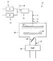
- FIG. 1is schematic diagram of an exemplary system usable in accordance with an aspect of the invention.
- FIG. 2a diagrammatic sectional view of a semiconductor wafer fragment in process in accordance with an aspect of the invention.
- FIG. 3is a diagrammatic sectional view of an alternate embodiment semiconductor wafer fragment in process in accordance with an aspect of the invention.
- FIG. 4is a diagrammatic sectional view of another alternate embodiment semiconductor wafer fragment in process in accordance with an aspect of the invention.
- the prior artrecognizes the desirability in certain instances of fabricating barium strontium titanate dielectric regions of capacitors to have variable concentration at different elevational locations in the thickness of such regions of barium and strontium.
- the typical prior art method of providing variable stoichiometry of barium and strontium at selected locations within the thickness of a barium strontium titanate dielectric regionis to vary the flows of the barium and strontium precursors to the reactor during a chemical vapor deposition (which may or may not be plasma enhanced). For example, increasing or decreasing the flow of the barium precursor or the strontium precursor will impact the atomic ratio of barium to strontium in the deposited barium strontium titanate layer. In some instances, separate barium and strontium precursors are mixed in the vapor phase, and the vapor mixture is flowed to the reactor.
- FIG. 1diagrammatically illustrates but one chemical vapor deposition system 10 in accordance with but one implementation of a chemical vapor deposition method in accordance with an aspect of the invention.
- Suchcomprises an A precursor feed stream 12 and a B precursor feed stream 14 .
- Suchcombine and feed to a vaporizer 16 .
- An inert gas stream 18can also be provided to vaporizer 16 to facilitate flow of the vaporized precursors to a downstream chamber.
- a chemical vapor deposition chamber 20is connected downstream of vaporizer 16 . Such includes a showerhead 22 for receiving and distributing gaseous precursors therein. A suitable wafer holder 24 is received within chamber 20 . Oxidizer gas feed streams, for example two oxidizer feed streams C and D, are preferably provided upstream of the showerhead. Further, an additional inert gas feed stream 19 is shown positioned between the oxidizer feed streams and chamber. More or less feed streams with or without mixing might also of course be utilized.
- the depositionis preferably conducted at subatmospheric pressure, with a vacuum pump 26 and an exemplary valve 28 being diagrammatically illustrated for achieving a desired vacuum pressure within chamber 20 . Further, the deposition may or may not be plasma enhanced.
- the A streamconsists essentially of a mixture of Ba and Sr precursors (i.e., preferably about 50%-50% by volume), and the B stream consists essentially of Ti precursor(s).
- Example preferred depositionis by metal organic chemical vapor deposition (MOCVD) processes, with at least one oxidizer being provided within chamber 20 with suitable MOCVD precursors to deposit a desired barium strontium titanate comprising dielectric layer.
- MOCVDmetal organic chemical vapor deposition
- Example precursorsinclude: Ba(thd) 2 bis(tetramethylheptanedionate) Sr(thd) 2 bis(tetramethylheptanedionate) Ti(thd) 2 (O-i-Pr) 2 (isopropoxide)bis(tetramethylheptanedionate) Ba(thd) 2 bis(tetramethylheptanedionate) Sr(thd) 2 bis(tetramethylheptanedionate) Ti(dmae) 4 bis(dimethylaminoethoxide) Ba(methd) 2 bis(methoxyethoxyte, hetramethylheptanedionate) Sr(methd) 2 bis(methoxyethoxyte, tetramethylheptanedionate) Ti(mpd)(thd) 2 bis(methylpentanediol, tetramethylheptanedionate) Ba(dpm) 2
- Adductsi.e., tetraglyme, trietherdiamine, pentamethyldiethlyenetriamine
- solventsi.e., butylacetate, methanol, tetrahydrofuran
- flow rates for the various of such precursorsinclude anywhere from 10 mg/min. to 1000 mg/min. of liquid feed to any suitable vaporizer.
- FIG. 2depicts an exemplary substrate 110 comprising a bulk monocrystalline silicon substrate 112 .
- semiconductor substrateor “semiconductive substrate” is defined to mean any construction comprising semiconductive material, including, but not limited to, bulk semiconductive materials such as a semiconductive wafer (either alone or in assemblies comprising other materials thereon), and semiconductive material layers (either alone or in assemblies comprising other materials).
- substraterefers to any supporting structure, including, but not limited to, the semiconductive substrates described above.
- An insulative layer 114such as borophosphosilicate glass (BPSG) by way of example only, is formed over substrate 112 .
- a conductive capacitor electrode layer 116such as platinum or an alloy thereof by way of example only, is formed over layer 114 .
- Such substrateis placed within a chemical vapor deposition reactor.
- Plasmaremote or within the chamber, might be utilized.
- Barium and strontiumare provided within the reactor by flowing at least one metal organic precursor to the reactor. Titanium is also provided within the reactor. By way of example only, exemplary precursors are as described above.
- At least one oxidizeris also flowed to the reactor. Conditions are provided within the reactor effective to deposit a barium strontium titanate comprising dielectric layer 118 on the substrate.
- the barium and strontiumare provided within the reactor during all of the deposit of layer 118 at a substantially constant atomic ratio of barium to strontium.
- a “substantially constant atomic ratio” of the barium and strontium in vapor phase within the reactoris to be interpreted as being from identically the same to within 5% atomic.
- a rate of flow of the oxidizeris changed at least once to effect a change in relative atomic concentration of barium and strontium within the deposited barium strontium titanate comprising dielectric layer.
- a rate of flow of the oxidizer to the reactoris changed at least once to effect a change in atomic concentration of titanium within the deposited barium strontium titanate comprising dielectric layer.
- the barium and strontiumare provided within the reactor during all of the deposit of the layer 118 at substantially constant volumetric flow rates to the reactor.
- substantially constant volumetric flow ratesare to be interpreted as being from exactly constant volumetric flow rates to within 5% volumetric.
- the barium and strontiumare provided within the reactor by flowing at least two metal organic precursors to the reactor, with one of the precursors comprising barium, and another of the precursors comprising strontium.
- Such precursorsmight be fed to the reactor as separate flow streams, or as a mixture in a single flow stream, as depicted by FIG. 1 and described above with respect to stream 12 .
- Preferred oxidizersare inorganic. Exemplary oxidizers include NO x , where “x” is at least 1 , N 2 O, O 2 , O 3 , H 2 O and H 2 O 2 .
- An inert gas, for example Armight also be flowed to chamber 20 from feed line 19 .
- the oxidizercomprises a single inorganic oxidizer consisting essentially of NO.
- flow rate of the oxidizer(s) and flow rate of the metal organic precursor(s)are provided to the reactor under some suitable set of conditions effective to deposit a substantially homogenous first portion 120 of barium strontium titanate.
- Some aspect of the rate of flow of the oxidizer(s)i.e., the rate of flow of one or more oxidizers to the reactor
- regions 120 and 122 of layer 18 while constituting barium strontium titanatehave different relative atomic ratios of barium and strontium, and/or titanium. Ratios of barium to strontium in the deposited layer might vary anywhere from 1% to 99% barium versus strontium. Accordingly in one aspect of the invention, the processor is able to vary the barium and strontium ratio in a barium strontium titanate layer by varying flow of the oxidizer as opposed to varying one or more flows of the barium and strontium precursors.
- FIG. 3illustrates an alternate embodiment wafer fragment 110 a .
- FIG. 3depicts barium strontium titanate comprising dielectric layer 118 a formed by oxidizer flow rate changes occurring in multiple discrete steps, thereby producing deposited layer 118 a to have three portions 124 , 126 and 128 . Such portions are characterized by at least two different barium and strontium concentration regions. Accordingly, FIG. 3 depicts changing rate of flow of the oxidizer(s) at least twice. Accordingly by way of example only, region 124 and 128 may be of the same composition, with region 126 therebetween being different. Alternately by way of example only, all three regions might be different in barium strontium and/or titanium composition.
- the inventionalso contemplates continuously varying of the oxidizer(s) flow effective to produce a gradient in barium-strontium, and/or titanium, concentration across at least some portion of the thickness of the deposited layer.
- An exemplary construction produced therebyis described with reference to FIG. 4 in connection with a substrate 110 b .
- Like numerals from the first described embodimentare utilized where appropriate, with differences being indicated with the suffix “b” or with different numerals.
- Variable relative concentration of barium and strontium in the illustrated layer 118 bis depicted by the increase in density across an increase in gradient from low to high of the illustrated dots or peppering of the illustrated layer 118 b .
- FIG. 4also illustrates the entirety of the thickness of layer 118 b having been processed to produce variable barium and strontium concentration throughout the entirety of the layer. Alternately, only a majority or some smaller portion thereof might be produced to have a non-homogenous construction. Further, and by way of example only, any of the example FIG. 2 and FIG. 3 constructions might be processed to include some portion which includes a concentration gradient thereacross, as opposed to the specific embodiment described above with respect to homogeneity in the subject regions.
- barium and strontiumare provided within the reactor by flowing at least one metal organic precursor to the reactor, and flowing oxidizers comprising at least O 3 and NO X to the reactor, where “x” is at least 1. Conditions are maintained effective to deposit a barium strontium titanate comprising dielectric layer on the substrate from such precursor(s). Additional oxidizers, including additional inorganic oxidizers, can be flowed to the reactor during the deposit.
- the flowing oxidizerscomprise at least O 2 and NO X , where “x” is at least one.
- Preferred total flows of the oxidizersinclude anywhere from 100 sccm to 4000 sccm, more preferably between 500 sccm and 2000 sccm, and more preferably between 750 sccm and 1250 sccm. Such flow rates and reduction to practice of the invention are with respect to an Applied Materials Centura Frame processor.
- a preferred pressure rangeis from 100 mtorr to 20 Torr, with a range of from 1 Torr to 6 Torr believed to be most preferred.
- Susceptor temperatureis preferably from 100° C. to 700° C., more preferably from 400° C. to 700° C., with less than or equal to 550° C.
- Utilization of O 2only tended to decrease the atomic percent concentration of titanium in the titanate, while deposition rate tended to increase. Using approximately 100% O 3 as the oxidizer, tended to increase the atomic percent of titanium in the titanate, while reducing the deposition rate significantly. Utilization of N 2 O as a sole oxidizer also tended to increase the atomic percent of titanium in the titanate, and reduce the deposition rate significantly. Utilization of NO as the sole oxidizer tended to increase titanium concentration in the titanate but produced only about 5 atomic percent barium, 57 atomic percent strontium, and 38 atomic percent titanium as the metals in the titanate layer. Further, deposition rate was reduced significantly over the control.
- O 2 as an oxidizertends to decrease atomic percent titanium yet increases the deposition rate by almost double that of O 3 , NO, N 2 O.
- O 3 and N 2 O as individual oxidizersappear to have similar deposition rate and similar composition in the system analyzed. They both increase atomic percent titanium in the titanate, and reduce the deposition rate significantly.
- NO as a sole oxidizerapparently results in low incorporation of barium, with the film constituting mostly Sr and Ti as the metals. Accordingly, increasing concentrations of NO may result in very low barium incorporations in barium strontium titanate films.
- the deposition rate with NO aloneis similar to that of O 3 and N 2 O.
- composition gradients across a barium strontium titanate filmcan be adjusted without changing the flow rates of the barium, strontium and titanium precursor sources.
- Other aspects of the inventioninclude various recited combination of oxidizers as literally claimed independent of the barium, strontium and titanium precursor feeds.
Landscapes
- Chemical & Material Sciences (AREA)
- General Chemical & Material Sciences (AREA)
- Chemical Kinetics & Catalysis (AREA)
- Engineering & Computer Science (AREA)
- Materials Engineering (AREA)
- Mechanical Engineering (AREA)
- Metallurgy (AREA)
- Organic Chemistry (AREA)
- Inorganic Chemistry (AREA)
- Formation Of Insulating Films (AREA)
- Chemical Vapour Deposition (AREA)
- Semiconductor Memories (AREA)
Abstract
Description
- This invention relates to chemical vapor deposition methods of forming barium strontium titanate comprising dielectric layers, including such layers having varied concentration of barium and strontium within the layer.[0001]
- As DRAMs increase in memory cell density, there is a continuing challenge to maintain sufficiently high storage capacitance despite decreasing cell area. Additionally, there is a continuing goal to further decrease cell area. One principal way of increasing cell capacitance is through cell structure techniques. Such techniques include three-dimensional cell capacitors, such as trenched or stacked capacitors. Yet as feature size continues to become smaller and smaller, development of improved materials for cell dielectrics as well as the cell structure are important. The feature size of 256Mb DRAMs and beyond will be on the order of 0.25 micron or less, and conventional dielectrics such as SiO[0002]2and Si3N4might not be suitable because of small dielectric constants.
- Highly integrated memory devices are expected to require a very thin dielectric film for the 3-dimensional capacitor of cylindrically stacked or trench structures. To meet this requirement, the capacitor dielectric film thickness will be below 2.5nm of SiO[0003]2equivalent thickness.
- Insulating inorganic metal oxide materials (such as ferroelectric materials, perovskite materials and pentoxides) are commonly referred to as “high k” materials due to their high dielectric constants, which make them attractive as dielectric materials in capacitors, for example for high density DRAMs and non-volatile memories. Using such materials enables the creation of much smaller and simpler capacitor structures for a given stored charge requirement, enabling the packing density dictated by future circuit design. One such known material is barium strontium titanate.[0004]
- The invention comprises in one aspect a chemical vapor deposition method of forming a barium strontium titanate comprising dielectric layer. A substrate is positioned within a chemical vapor deposition reactor. Barium and strontium are provided within the reactor by flowing at least one metal organic precursor to the reactor. Titanium is provided within the reactor. At least one oxidizer is flowed to the reactor. Conditions are provided within the reactor to be effective to deposit a barium strontium titanate comprising dielectric layer on the substrate from the reactants. The barium and strontium are provided within the reactor during all of the deposit of said layer at a substantially constant atomic ratio of barium to strontium. During the deposit a rate of flow of the oxidizer to the reactor is changed at least once to effect a change in relative atomic concentration of barium and strontium within the deposited barium strontium titanate comprising dielectric layer. In one aspect, during the deposit a rate of flow of the oxidizer to the reactor is changed at least once to effect a change in atomic concentration of titanium within the deposited barium strontium titanate comprising dielectric layer.[0005]
- In other aspects, barium and strontium are provided within the reactor by flowing at least one metal organic precursor to the reactor. Titanium is provided within the reactor. Multiple oxidizers are flowed to the reactor. Conditions are provided within the reactor to be effective to deposit a barium strontium titanate comprising dielectric layer on the substrate from the reactants. In one embodiment, the oxidizers comprise at least O[0006]3and N2, with the O3being present within the reactor during at least a portion of the deposit at greater than 10% by volume of the total volume of N2and O3within the reactor. In one embodiment, the oxidizers comprise at least O3and NOx, where “x” is at least 1. In one embodiment, the oxidizers comprise at least O2and NOx, where “x” is at least 1. In one embodiment, the oxidizers comprise at least N2O and NOx, where “x” is at least 1.
- Other embodiments are contemplated.[0007]
- Preferred embodiments of the invention are described below with reference to the following accompanying drawings.[0008]
- FIG. 1 is schematic diagram of an exemplary system usable in accordance with an aspect of the invention.[0009]
- FIG. 2 a diagrammatic sectional view of a semiconductor wafer fragment in process in accordance with an aspect of the invention.[0010]
- FIG. 3 is a diagrammatic sectional view of an alternate embodiment semiconductor wafer fragment in process in accordance with an aspect of the invention.[0011]
- FIG. 4 is a diagrammatic sectional view of another alternate embodiment semiconductor wafer fragment in process in accordance with an aspect of the invention.[0012]
- This disclosure of the invention is submitted in furtherance of the constitutional purposes of the U.S. Patent Laws “to promote the progress of science and useful arts” (Article 1, Section 8).[0013]
- The prior art recognizes the desirability in certain instances of fabricating barium strontium titanate dielectric regions of capacitors to have variable concentration at different elevational locations in the thickness of such regions of barium and strontium. The typical prior art method of providing variable stoichiometry of barium and strontium at selected locations within the thickness of a barium strontium titanate dielectric region is to vary the flows of the barium and strontium precursors to the reactor during a chemical vapor deposition (which may or may not be plasma enhanced). For example, increasing or decreasing the flow of the barium precursor or the strontium precursor will impact the atomic ratio of barium to strontium in the deposited barium strontium titanate layer. In some instances, separate barium and strontium precursors are mixed in the vapor phase, and the vapor mixture is flowed to the reactor.[0014]
- FIG. 1 diagrammatically illustrates but one chemical[0015]
vapor deposition system 10 in accordance with but one implementation of a chemical vapor deposition method in accordance with an aspect of the invention. Such comprises an Aprecursor feed stream 12 and a Bprecursor feed stream 14. Such combine and feed to avaporizer 16. Aninert gas stream 18 can also be provided tovaporizer 16 to facilitate flow of the vaporized precursors to a downstream chamber. - A chemical[0016]
vapor deposition chamber 20 is connected downstream ofvaporizer 16. Such includes ashowerhead 22 for receiving and distributing gaseous precursors therein. Asuitable wafer holder 24 is received withinchamber 20. Oxidizer gas feed streams, for example two oxidizer feed streams C and D, are preferably provided upstream of the showerhead. Further, an additional inertgas feed stream 19 is shown positioned between the oxidizer feed streams and chamber. More or less feed streams with or without mixing might also of course be utilized. The deposition is preferably conducted at subatmospheric pressure, with avacuum pump 26 and anexemplary valve 28 being diagrammatically illustrated for achieving a desired vacuum pressure withinchamber 20. Further, the deposition may or may not be plasma enhanced. - In one example, and by way of example only, the A stream consists essentially of a mixture of Ba and Sr precursors (i.e., preferably about 50%-50% by volume), and the B stream consists essentially of Ti precursor(s). Example preferred deposition is by metal organic chemical vapor deposition (MOCVD) processes, with at least one oxidizer being provided within[0017]
chamber 20 with suitable MOCVD precursors to deposit a desired barium strontium titanate comprising dielectric layer. Example precursors, and by way of example only, include:Ba(thd)2 bis(tetramethylheptanedionate) Sr(thd)2 bis(tetramethylheptanedionate) Ti(thd)2(O-i-Pr)2 (isopropoxide)bis(tetramethylheptanedionate) Ba(thd)2 bis(tetramethylheptanedionate) Sr(thd)2 bis(tetramethylheptanedionate) Ti(dmae)4 bis(dimethylaminoethoxide) Ba(methd)2 bis(methoxyethoxyte, hetramethylheptanedionate) Sr(methd)2 bis(methoxyethoxyte, tetramethylheptanedionate) Ti(mpd)(thd)2 bis(methylpentanediol, tetramethylheptanedionate) Ba(dpm)2 bis(dipivaloylmethanato) Sr(dpm)2 bis(dipivaloylmethanato) TiO(dpm)2 (titanyl)bis(dipivaloylmethanato) Ba(dpm)2 bis(dipivaloylmethanato) Sr(dpm)2 bis(dipivaloylmethanato) Ti(t-BuO)2(dpm)2 (t-butoxy)bis(dipivaloylmethanato) Ba(dpm)2 bis(dipivaloylmethanato) Sr(dpm)2 bis(dipivaloylmethanato) Ti(OCH3)2(dpm)2 (methoxy)bis(dipivaloylmethanato) - Adducts (i.e., tetraglyme, trietherdiamine, pentamethyldiethlyenetriamine), solvents (i.e., butylacetate, methanol, tetrahydrofuran), and/or other materials might be utilized with the precursors. By way of example only, and where the precursors include metal organic precursors, example flow rates for the various of such precursors include anywhere from 10 mg/min. to 1000 mg/min. of liquid feed to any suitable vaporizer.[0018]
- A first aspect of the invention is described in connection with a chemical vapor deposition method of forming a barium strontium titanate comprising dielectric layer. By way of example only, three exemplary implementations are described with reference to FIGS.[0019]2-4. FIG. 2 depicts an
exemplary substrate 110 comprising a bulkmonocrystalline silicon substrate 112. In the context of this document, the term “semiconductor substrate” or “semiconductive substrate” is defined to mean any construction comprising semiconductive material, including, but not limited to, bulk semiconductive materials such as a semiconductive wafer (either alone or in assemblies comprising other materials thereon), and semiconductive material layers (either alone or in assemblies comprising other materials). The term “substrate” refers to any supporting structure, including, but not limited to, the semiconductive substrates described above. Aninsulative layer 114, such as borophosphosilicate glass (BPSG) by way of example only, is formed oversubstrate 112. A conductivecapacitor electrode layer 116, such as platinum or an alloy thereof by way of example only, is formed overlayer 114. - Such substrate is placed within a chemical vapor deposition reactor. Plasma, remote or within the chamber, might be utilized. Barium and strontium are provided within the reactor by flowing at least one metal organic precursor to the reactor. Titanium is also provided within the reactor. By way of example only, exemplary precursors are as described above. At least one oxidizer is also flowed to the reactor. Conditions are provided within the reactor effective to deposit a barium strontium titanate comprising[0020]
dielectric layer 118 on the substrate. - In accordance with but one aspect of the invention, the barium and strontium are provided within the reactor during all of the deposit of[0021]
layer 118 at a substantially constant atomic ratio of barium to strontium. In the context of this document, a “substantially constant atomic ratio” of the barium and strontium in vapor phase within the reactor is to be interpreted as being from identically the same to within 5% atomic. In but one embodiment, during the deposit a rate of flow of the oxidizer is changed at least once to effect a change in relative atomic concentration of barium and strontium within the deposited barium strontium titanate comprising dielectric layer. Further in but one embodiment, during the deposit a rate of flow of the oxidizer to the reactor is changed at least once to effect a change in atomic concentration of titanium within the deposited barium strontium titanate comprising dielectric layer. Preferably in addition to providing a substantially constant atomic ratio of barium and strontium during all of the deposit, the barium and strontium are provided within the reactor during all of the deposit of thelayer 118 at substantially constant volumetric flow rates to the reactor. In the context of this document, “substantially constant volumetric flow rates” are to be interpreted as being from exactly constant volumetric flow rates to within 5% volumetric. - In one preferred embodiment, the barium and strontium are provided within the reactor by flowing at least two metal organic precursors to the reactor, with one of the precursors comprising barium, and another of the precursors comprising strontium. Such precursors might be fed to the reactor as separate flow streams, or as a mixture in a single flow stream, as depicted by FIG. 1 and described above with respect to stream[0022]12. Preferred oxidizers are inorganic. Exemplary oxidizers include NOx, where “x” is at least1, N2O, O2, O3, H2O and H2O2. An inert gas, for example Ar, might also be flowed to
chamber 20 fromfeed line 19. In one aspect of the invention, at least two inorganic oxidizers are flowed to the reactor, such as various combinations of the above described oxidizers. In one aspect of the invention, the oxidizer comprises a single inorganic oxidizer consisting essentially of NO. - In the exemplary depicted FIG. 2 example, flow rate of the oxidizer(s) and flow rate of the metal organic precursor(s) are provided to the reactor under some suitable set of conditions effective to deposit a substantially homogenous[0023]
first portion 120 of barium strontium titanate. Some aspect of the rate of flow of the oxidizer(s) (i.e., the rate of flow of one or more oxidizers to the reactor) is changed to affect a change in relative atomic concentration of barium and strontium, and/or titanium, for example to deposit a substantially homogenoussecond portion 122 of bariumstrontium titanate layer 118. Accordinglyregions layer 18 while constituting barium strontium titanate have different relative atomic ratios of barium and strontium, and/or titanium. Ratios of barium to strontium in the deposited layer might vary anywhere from 1% to 99% barium versus strontium. Accordingly in one aspect of the invention, the processor is able to vary the barium and strontium ratio in a barium strontium titanate layer by varying flow of the oxidizer as opposed to varying one or more flows of the barium and strontium precursors. - For example in reduction to practice examples, increasing quantities of NO as an oxidizer was discovered to reduce barium incorporation in barium strontium titanate films using a substantially constant premixed 50%/5[0024]0% by volume feed of barium and strontium precursors as described above. It was also discovered that increasing NO feed also increased deposition rate and reduced carbon incorporation in the deposited layer. Accordingly, barium to strontium ratio in a barium strontium titanate film can be modified without changing any aspect of the barium strontium precursor feeds.
- FIG. 3 illustrates an alternate embodiment wafer fragment[0025]110a. Like numerals from the first described embodiment are utilized where appropriate, with differences being indicated with the suffix “a” or with different numerals. FIG. 3 depicts barium strontium titanate comprising
dielectric layer 118aformed by oxidizer flow rate changes occurring in multiple discrete steps, thereby producing depositedlayer 118ato have threeportions region region 126 therebetween being different. Alternately by way of example only, all three regions might be different in barium strontium and/or titanium composition. - The invention also contemplates continuously varying of the oxidizer(s) flow effective to produce a gradient in barium-strontium, and/or titanium, concentration across at least some portion of the thickness of the deposited layer. An exemplary construction produced thereby is described with reference to FIG. 4 in connection with a substrate[0026]110b. Like numerals from the first described embodiment are utilized where appropriate, with differences being indicated with the suffix “b” or with different numerals. Variable relative concentration of barium and strontium in the illustrated
layer 118bis depicted by the increase in density across an increase in gradient from low to high of the illustrated dots or peppering of the illustratedlayer 118b. FIG. 4 also illustrates the entirety of the thickness oflayer 118bhaving been processed to produce variable barium and strontium concentration throughout the entirety of the layer. Alternately, only a majority or some smaller portion thereof might be produced to have a non-homogenous construction. Further, and by way of example only, any of the example FIG. 2 and FIG. 3 constructions might be processed to include some portion which includes a concentration gradient thereacross, as opposed to the specific embodiment described above with respect to homogeneity in the subject regions. - Other aspects of the invention are described below in connection with chemical vapor deposition methods of forming a barium strontium titanate comprising dielectric layer regardless of whether such has a varying concentration of barium and strontium within the layer, regardless of changing flow rate of an oxidizer, and regardless of whether a substantially constant atomic ratio of barium and strontium is provided in the reactor during deposit of the layer. In a first additional aspect of the invention, barium and strontium are provided within the reactor by flowing at least one metal organic precursor to the reactor, and flowing oxidizers comprising at least O[0027]3and NOXto the reactor, where “x” is at least 1. Conditions are maintained effective to deposit a barium strontium titanate comprising dielectric layer on the substrate from such precursor(s). Additional oxidizers, including additional inorganic oxidizers, can be flowed to the reactor during the deposit.
- In another embodiment, the flowing oxidizers comprise at least O[0028]2and NOX, where “x” is at least one.
- In other embodiments, the flowing oxidizers comprise at least N[0029]2O and at least one of NOXand O3, where “x” is at least one. Where NOxis utilized, it is ideally present within the reactor during at least a portion of the deposit at greater than 10% by volume of the total volume of N2O and NOxwithin the reactor. Where O3is utilized, it is ideally present within the reactor during at least a portion of the deposit at greater than 10% by volume of the total volume of N2O and O3within the reactor during the deposit. Additional oxidizers might also be utilized in combination with one or both of the O3and NOx. By way of example, a combination of three oxidizers flowed to the reactor includes at least O2, O3and NOx. An alternate example includes O2, O3and N2O. Use of additional oxidizers is of also course contemplated.
- Preferred total flows of the oxidizers include anywhere from 100 sccm to 4000 sccm, more preferably between 500 sccm and 2000 sccm, and more preferably between 750 sccm and 1250 sccm. Such flow rates and reduction to practice of the invention are with respect to an Applied Materials Centura Frame processor. A preferred pressure range is from 100 mtorr to 20 Torr, with a range of from 1 Torr to 6 Torr believed to be most preferred. Susceptor temperature is preferably from 100° C. to 700° C., more preferably from 400° C. to 700° C., with less than or equal to 550° C. being even more preferred, particularly in obtaining continuity in the deposited layer at a thickness at or below 200 Angstroms, and preferably at least down to 50 Angstroms. Most preferably, the susceptor temperature is kept at less than or equal to 550° C. during all of the deposit to form the subject layer. An inert gas, such as Ar, is also preferably flowed to the reactor downstream of the oxidizer feeds, and preferably at substantially the same flow rate as the total oxidizer flow rate.[0030]
- The following effects are noted relative to oxide combinations. Such are provided by way of illustration only with respect to reduction to practice examples at 3 Torr, at a susceptor temperature of 500° C., and in an Applied Materials Centura reactor. Such are provided by way of illustration only, and in no way as limitations to be read into any of the accompanying claims. All comparisons below are with respect to a 50:50 volumetric ratio control feed of O[0031]2and N2O as the oxidizers.
- Utilization of O[0032]2only tended to decrease the atomic percent concentration of titanium in the titanate, while deposition rate tended to increase. Using approximately 100% O3as the oxidizer, tended to increase the atomic percent of titanium in the titanate, while reducing the deposition rate significantly. Utilization of N2O as a sole oxidizer also tended to increase the atomic percent of titanium in the titanate, and reduce the deposition rate significantly. Utilization of NO as the sole oxidizer tended to increase titanium concentration in the titanate but produced only about 5 atomic percent barium, 57 atomic percent strontium, and 38 atomic percent titanium as the metals in the titanate layer. Further, deposition rate was reduced significantly over the control.
- Feeding a combination of O[0033]2and O3in a 1:1 volumetric ratio tended to decrease the titanium incorporation into the titanate, but increase the deposition rate. Using O2and N2O in combination in a 1:1 volumetric ratio tends to decrease titanium incorporation in the titanate, and increase the deposition rate. Utilization of N2O and O3in a 6:1 volumetric ratio also tended to increase the titanium incorporation in the titanate, but significantly reduced the deposition rate. Decreasing the deposition temperature (i.e., to below 600° C.) resulted in increased carbon content.
- Utilization of a combination of NO and O[0034]2in a volumetric ratio of 1:1 increased titanium concentration significantly to 95%, and reduced strontium incorporation to about 1 atomic percent and barium incorporation to 4%. Deposition rate was also drastically reduced.
- Utilization of NO and O[0035]3in a volumetric ratio of 1:1 increases titanium incorporation and also provided 17 atomic percent barium and 44 atomic percent strontium in the resultant titanate film. Deposition rate however was reduced over the control oxidizer mixture.
- Deposition of barium strontium titanate films in the presence of an O[0036]3(93% O2, 7% O3) and Ar mixture caused the film composition to be somewhat self-adjusted. In other words, process conditions do not show a strong influence on film composition even when using different precursor flows for the barium, strontium and titanium. This is expected to result in a process of depositing barium strontium titanate of a given composition having a large process window. This should also facilitate formation of barium strontium titanate films over varying topography with negligible variation of stoichiometry over the sidewalls.
- General observations were that O[0037]2as an oxidizer tends to decrease atomic percent titanium yet increases the deposition rate by almost double that of O3, NO, N2O. O3and N2O as individual oxidizers appear to have similar deposition rate and similar composition in the system analyzed. They both increase atomic percent titanium in the titanate, and reduce the deposition rate significantly.
- NO as a sole oxidizer apparently results in low incorporation of barium, with the film constituting mostly Sr and Ti as the metals. Accordingly, increasing concentrations of NO may result in very low barium incorporations in barium strontium titanate films. The deposition rate with NO alone is similar to that of O[0038]3and N2O.
- When O[0039]2, O3and N2O are combined, the following were observed. The affect of N2O is insignificant in terms of composition or deposition rate, as the results were very similar to the O2and O3runs. O2appears to control the deposition rate, because the runs with O2have higher deposition rates. Use of O2, O3and N2O appeared to have no significant impact on the barium to strontium ratio in the titanate film.
- When O[0040]2, O3and NO were combined, the following was observed. NO alone produced a film that had little atomic percent barium incorporation. While adding O3with NO, the ozone enabled more barium incorporation, but had little effect on titanium incorporation. O2and NO results are similar to O2, O3and NO, with the film being approximately 95% titanium, with less than 1% strontium, and approximately 4% barium. This indicates that O2and NO together apparently deplete strontium incorporation. The use of O2appeared to control the deposition rate, because the runs with O2had higher deposition rates.
- In one aspect of the invention, composition gradients across a barium strontium titanate film can be adjusted without changing the flow rates of the barium, strontium and titanium precursor sources. Other aspects of the invention include various recited combination of oxidizers as literally claimed independent of the barium, strontium and titanium precursor feeds.[0041]
- Additional and/or alternate preferred processing can occur in accordance with any of our co-pending U.S. patent application Ser. No. 09/476,516, filed on Jan. 3, 2000, entitled “Chemical Vapor Deposition Methods Of Forming A High K Dielectric Layer And Methods Of Forming A Capacitor”, listing Cem Basceri as inventor; U.S. patent application Ser. No. 09/580,733, filed on May 26, 2000, entitled “Chemical Vapor Deposition Methods And Physical Vapor Deposition Methods”, listing Cem Basceri as inventor; and U.S. patent application Ser. No. 09/______, filed concurrently herewith, entitled “Chemical Vapor Deposition Methods Of Forming Barium Strontium Titanate Comprising Dielectric Layers”, listing Cem Basceri and Nancy Alzola as inventors. Each of these is hereby fully incorporated by reference.[0042]
- In compliance with the statute, the invention has been described in language more or less specific as to structural and methodical features. It is to be understood, however, that the invention is not limited to the specific features shown and described, since the means herein disclosed comprise preferred forms of putting the invention into effect. The invention is, therefore, claimed in any of its forms or modifications within the proper scope of the appended claims appropriately interpreted in accordance with the doctrine of equivalents.[0043]
Claims (51)
1. A chemical vapor deposition method of forming a barium strontium titanate comprising dielectric layer having a varied concentration of barium and strontium within the layer, comprising:
positioning a substrate within a chemical vapor deposition reactor;
providing barium and strontium within the reactor by flowing at least one metal organic precursor to the reactor, and providing titanium within the reactor, and flowing at least one oxidizer to the reactor, under conditions effective to deposit a barium strontium titanate comprising dielectric layer on the substrate; the barium and strontium being provided within the reactor during all of the deposit of said layer at a substantially constant atomic ratio of barium to strontium; and
during said deposit, changing a rate of flow of the oxidizer to the reactor at least once to effect a change in relative atomic concentration of barium and strontium within the deposited barium strontium titanate comprising dielectric layer.
2. The method ofclaim 1 comprising changing the rate of flow at least twice.
3. The method ofclaim 1 comprising providing the barium and strontium within the reactor by flowing at least two metal organic precursors to the reactor, one of the precursors comprising barium, another of the precursors comprising strontium.
4. The method ofclaim 1 comprising providing the barium and strontium within the reactor by flowing at least two metal organic precursors to the reactor, one of the precursors comprising barium, another of the precursors comprising strontium, the one and the another precursors being fed to the reactor as a mixture in a single flow stream.
5. The method ofclaim 1 comprising providing the barium and strontium within the reactor during all of the deposit of said layer at substantially constant volumetric flow rates to the reactor.
6. The method ofclaim 1 wherein the oxidizer is inorganic.
7. The method ofclaim 1 wherein the oxidizer comprises NOx, where “x” is at least 1.
8. The method ofclaim 1 wherein the oxidizer comprises NO.
9. The method ofclaim 1 wherein the oxidizer comprises a single inorganic oxidizer consisting essentially of NO.
10. The method ofclaim 1 comprising flowing at least two oxidizers to the reactor.
11. The method ofclaim 1 comprising flowing at least two inorganic oxidizers to the reactor.
12. The method ofclaim 1 comprising flowing at least two inorganic oxidizers to the reactor, said oxidizers comprising at least O3and N2O.
13. The method ofclaim 1 comprising flowing at least two inorganic oxidizers to the reactor, said oxidizers comprising at least O3and NOx, where “x” is at least 1.
14. The method ofclaim 1 comprising flowing at least two inorganic oxidizers to the reactor, said oxidizers comprising at least O2and NOx.
15. The method ofclaim 1 comprising flowing at least two inorganic oxidizers to the reactor, said oxidizers comprising at least O2and N2O.
16. The method ofclaim 1 comprising flowing at least two inorganic oxidizers to the reactor, said oxidizers comprising at least N2O and NOx, where “x” is at least 1.
17. A chemical vapor deposition method of forming a barium strontium titanate comprising dielectric layer having a varied concentration of titanium within the layer, comprising:
positioning a substrate within a chemical vapor deposition reactor;
providing barium and strontium within the reactor by flowing at least one metal organic precursor to the reactor, and providing titanium within the reactor, and flowing at least one oxidizer to the reactor, under conditions effective to deposit a barium strontium titanate comprising dielectric layer on the substrate; the barium and strontium being provided within the reactor during all of the deposit of said layer at a substantially constant atomic ratio of barium to strontium; and
during said deposit, changing a rate of flow of the oxidizer to the reactor at least once to effect a change in atomic concentration of titanium within the deposited barium strontium titanate comprising dielectric layer.
18. The method ofclaim 17 wherein the changing of a rate of flow of the oxidizer to the reactor at least once is also effective to effect a change in relative atomic concentration of barium and strontium within the deposited barium strontium titanate comprising dielectric layer.
19. The method ofclaim 17 comprising changing the rate of flow at least twice.
20. The method ofclaim 17 wherein the oxidizer is inorganic.
21. The method ofclaim 17 wherein the oxidizer comprises NOx, where “x” is at least 1.
22. The method ofclaim 17 wherein the oxidizer comprises NO.
23. The method ofclaim 17 wherein the oxidizer comprises a single inorganic oxidizer consisting essentially of NO.
24. The method ofclaim 17 comprising flowing at least two oxidizers to the reactor.
25. The method ofclaim 17 comprising flowing at least two inorganic oxidizers to the reactor.
26. A chemical vapor deposition method of forming a barium strontium titanate comprising dielectric layer, comprising:
positioning a substrate within a chemical vapor deposition reactor; and
providing barium and strontium within the reactor by flowing at least one metal organic precursor to the reactor, and providing titanium within the reactor, and flowing oxidizers comprising at least O3and N2O to the reactor, under conditions effective to deposit a barium strontium titanate comprising dielectric layer on the substrate; the O3being present within the reactor during at least a portion of the deposit at greater than 10% by volume of the total volume of N2O and O3within the reactor.
27. The method ofclaim 26 wherein the portion comprises a majority portion.
28. The method ofclaim 26 wherein the portion comprises all of the deposit.
29. The method ofclaim 26 wherein the conditions are void of plasma and remote plasma.
30. The method ofclaim 26 wherein the conditions comprise at least one of plasma or remote plasma.
31. The method ofclaim 26 comprising flowing another inorganic oxidizer to the reactor during the deposit.
32. A chemical vapor deposition method of forming a barium strontium titanate comprising dielectric layer, comprising:
positioning a substrate within a chemical vapor deposition reactor; and
providing barium and strontium within the reactor by flowing at least one metal organic precursor to the reactor, and providing titanium within the reactor, and flowing oxidizers comprising at least O3and NOxto the reactor, where “x” is at least 1, under conditions effective to deposit a barium strontium titanate comprising dielectric layer on the substrate.
33. The method ofclaim 32 wherein “x” equals 1.
34. The method ofclaim 32 wherein “x” is more than 1.
35. The method ofclaim 32 comprising flowing another inorganic oxidizer to the reactor during the deposit.
36. A chemical vapor deposition method of forming a barium strontium titanate comprising dielectric layer, comprising:
positioning a substrate within a chemical vapor deposition reactor; and
providing barium and strontium within the reactor by flowing at least one metal organic precursor to the reactor, and providing titanium within the reactor, and flowing oxidizers comprising at least O2and NOxto the reactor, where “x” is at least 1, under conditions effective to deposit a barium strontium titanate comprising dielectric layer on the substrate.
37. The method ofclaim 36 wherein “x” equals 1.
38. The method ofclaim 36 wherein “x” is more than 1.
39. The method ofclaim 36 comprising flowing another inorganic oxidizer to the reactor during the deposit.
40. A chemical vapor deposition method of forming a barium strontium titanate comprising dielectric layer, comprising:
positioning a substrate within a chemical vapor deposition reactor; and
providing barium and strontium within the reactor by flowing at least one metal organic precursor to the reactor, and providing titanium within the reactor, and flowing oxidizers comprising at least N2O and NOxto the reactor, where “x” is at least 1, under conditions effective to deposit a barium strontium titanate comprising dielectric layer on the substrate, the NOxbeing present within the reactor during at least a portion of the deposit at greater than 10% by volume of the total volume of N2O and NOxwithin the reactor.
41. The method ofclaim 40 wherein “x” equals 1.
42. The method ofclaim 40 wherein “x” is more than 1.
43. The method ofclaim 40 comprising flowing another inorganic oxidizer to the reactor during the deposit.
44. A chemical vapor deposition method of forming a barium strontium titanate comprising dielectric layer, comprising:
positioning a substrate within a chemical vapor deposition reactor; and
providing barium and strontium within the reactor by flowing at least one metal organic precursor to the reactor, and providing titanium within the reactor, and flowing oxidizers comprising at least O2, O3and NOxto the reactor, where “x” is at least 1, under conditions effective to deposit a barium strontium titanate comprising dielectric layer on the substrate.
45. The method ofclaim 44 wherein “x” equals 1.
46. The method ofclaim 44 wherein “x” is more than 1.
47. A chemical vapor deposition method of forming a barium strontium titanate comprising dielectric layer, comprising:
positioning a substrate within a chemical vapor deposition reactor; and
providing barium and strontium within the reactor by flowing at least one metal organic precursor to the reactor, and providing titanium within the reactor, and flowing oxidizers comprising at least O2, O3and N2O to the reactor, under conditions effective to deposit a barium strontium titanate comprising dielectric layer on the substrate.
48. The method ofclaim 47 wherein the conditions comprise receipt of the substrate by a susceptor, the susceptor having a temperature of less than or equal to 550° C.
49. The method ofclaim 47 wherein the deposited layer is substantially homogeneous.
50. The method ofclaim 47 wherein the deposited layer is not substantially homogeneous.
51. The method ofclaim 47 comprising flowing another inorganic oxidizer to the reactor during the deposit.
Priority Applications (3)
| Application Number | Priority Date | Filing Date | Title |
|---|---|---|---|
| US09/905,320US20030017266A1 (en) | 2001-07-13 | 2001-07-13 | Chemical vapor deposition methods of forming barium strontium titanate comprising dielectric layers, including such layers having a varied concentration of barium and strontium within the layer |
| US10/769,149US6982103B2 (en) | 2001-07-13 | 2004-01-30 | Chemical vapor deposition methods of forming barium strontium titanate comprising dielectric layers, including such layers having a varied concentration of barium and strontium within the layer |
| US10/876,703US7208198B2 (en) | 2001-07-13 | 2004-06-28 | Chemical vapor deposition methods of forming barium strontium titanate comprising dielectric layers, including such layers having a varied concentration of barium and strontium within the layer |
Applications Claiming Priority (1)
| Application Number | Priority Date | Filing Date | Title |
|---|---|---|---|
| US09/905,320US20030017266A1 (en) | 2001-07-13 | 2001-07-13 | Chemical vapor deposition methods of forming barium strontium titanate comprising dielectric layers, including such layers having a varied concentration of barium and strontium within the layer |
Related Child Applications (2)
| Application Number | Title | Priority Date | Filing Date |
|---|---|---|---|
| US10/769,149ContinuationUS6982103B2 (en) | 2001-07-13 | 2004-01-30 | Chemical vapor deposition methods of forming barium strontium titanate comprising dielectric layers, including such layers having a varied concentration of barium and strontium within the layer |
| US10/876,703ContinuationUS7208198B2 (en) | 2001-07-13 | 2004-06-28 | Chemical vapor deposition methods of forming barium strontium titanate comprising dielectric layers, including such layers having a varied concentration of barium and strontium within the layer |
Publications (1)
| Publication Number | Publication Date |
|---|---|
| US20030017266A1true US20030017266A1 (en) | 2003-01-23 |
Family
ID=25420627
Family Applications (3)
| Application Number | Title | Priority Date | Filing Date |
|---|---|---|---|
| US09/905,320AbandonedUS20030017266A1 (en) | 2001-07-13 | 2001-07-13 | Chemical vapor deposition methods of forming barium strontium titanate comprising dielectric layers, including such layers having a varied concentration of barium and strontium within the layer |
| US10/769,149Expired - Fee RelatedUS6982103B2 (en) | 2001-07-13 | 2004-01-30 | Chemical vapor deposition methods of forming barium strontium titanate comprising dielectric layers, including such layers having a varied concentration of barium and strontium within the layer |
| US10/876,703Expired - Fee RelatedUS7208198B2 (en) | 2001-07-13 | 2004-06-28 | Chemical vapor deposition methods of forming barium strontium titanate comprising dielectric layers, including such layers having a varied concentration of barium and strontium within the layer |
Family Applications After (2)
| Application Number | Title | Priority Date | Filing Date |
|---|---|---|---|
| US10/769,149Expired - Fee RelatedUS6982103B2 (en) | 2001-07-13 | 2004-01-30 | Chemical vapor deposition methods of forming barium strontium titanate comprising dielectric layers, including such layers having a varied concentration of barium and strontium within the layer |
| US10/876,703Expired - Fee RelatedUS7208198B2 (en) | 2001-07-13 | 2004-06-28 | Chemical vapor deposition methods of forming barium strontium titanate comprising dielectric layers, including such layers having a varied concentration of barium and strontium within the layer |
Country Status (1)
| Country | Link |
|---|---|
| US (3) | US20030017266A1 (en) |
Cited By (328)
| Publication number | Priority date | Publication date | Assignee | Title |
|---|---|---|---|---|
| US20030207472A1 (en)* | 2001-02-02 | 2003-11-06 | Micron Technology, Inc. | Method for controlling deposition of dielectric films |
| US20040185177A1 (en)* | 2001-07-13 | 2004-09-23 | Cem Basceri | Chemical vapor deposition methods of forming barium strontium titanate comprising dielectric layers, including such layers having a varied concentration of barium and strontium within the layer |
| US6838122B2 (en) | 2001-07-13 | 2005-01-04 | Micron Technology, Inc. | Chemical vapor deposition methods of forming barium strontium titanate comprising dielectric layers |
| US6884475B2 (en) | 2000-05-26 | 2005-04-26 | Micron Technology, Inc. | Chemical vapor deposition method for depositing a high k dielectric film |
| US6888188B2 (en) | 2001-08-17 | 2005-05-03 | Micron Technology, Inc. | Capacitor constructions comprising perovskite-type dielectric materials and having different degrees of crystallinity within the perovskite-type dielectric materials |
| US20050152094A1 (en)* | 2004-01-14 | 2005-07-14 | Jeong Yong-Kuk | Capacitor including a dielectric layer having an inhomogeneous crystalline region and method of fabricating the same |
| US20060006450A1 (en)* | 1999-08-30 | 2006-01-12 | Al-Shareef Husam N | Capacitors having a capacitor dielectric layer comprising a metal oxide having multiple different metals bonded with oxygen |
| US7033884B2 (en) | 2003-05-20 | 2006-04-25 | Micron Technology, Inc. | Methods of forming capacitor constructions |
| FR2970110A1 (en)* | 2010-12-29 | 2012-07-06 | St Microelectronics Crolles 2 | PROCESS FOR PRODUCING A POLYCRYSTALLINE DIELECTRIC LAYER |
| US20140346650A1 (en)* | 2009-08-14 | 2014-11-27 | Asm Ip Holding B.V. | Systems and methods for thin-film deposition of metal oxides using excited nitrogen-oxygen species |
| US10559458B1 (en) | 2018-11-26 | 2020-02-11 | Asm Ip Holding B.V. | Method of forming oxynitride film |
| US10561975B2 (en) | 2014-10-07 | 2020-02-18 | Asm Ip Holdings B.V. | Variable conductance gas distribution apparatus and method |
| USD876504S1 (en) | 2017-04-03 | 2020-02-25 | Asm Ip Holding B.V. | Exhaust flow control ring for semiconductor deposition apparatus |
| US10590535B2 (en) | 2017-07-26 | 2020-03-17 | Asm Ip Holdings B.V. | Chemical treatment, deposition and/or infiltration apparatus and method for using the same |
| US10600673B2 (en) | 2015-07-07 | 2020-03-24 | Asm Ip Holding B.V. | Magnetic susceptor to baseplate seal |
| US10604847B2 (en) | 2014-03-18 | 2020-03-31 | Asm Ip Holding B.V. | Gas distribution system, reactor including the system, and methods of using the same |
| US10612136B2 (en) | 2018-06-29 | 2020-04-07 | ASM IP Holding, B.V. | Temperature-controlled flange and reactor system including same |
| US10622375B2 (en) | 2016-11-07 | 2020-04-14 | Asm Ip Holding B.V. | Method of processing a substrate and a device manufactured by using the method |
| US10643904B2 (en) | 2016-11-01 | 2020-05-05 | Asm Ip Holdings B.V. | Methods for forming a semiconductor device and related semiconductor device structures |
| US10643826B2 (en) | 2016-10-26 | 2020-05-05 | Asm Ip Holdings B.V. | Methods for thermally calibrating reaction chambers |
| US10658205B2 (en) | 2017-09-28 | 2020-05-19 | Asm Ip Holdings B.V. | Chemical dispensing apparatus and methods for dispensing a chemical to a reaction chamber |
| US10658181B2 (en) | 2018-02-20 | 2020-05-19 | Asm Ip Holding B.V. | Method of spacer-defined direct patterning in semiconductor fabrication |
| US10655221B2 (en) | 2017-02-09 | 2020-05-19 | Asm Ip Holding B.V. | Method for depositing oxide film by thermal ALD and PEALD |
| US10665452B2 (en) | 2016-05-02 | 2020-05-26 | Asm Ip Holdings B.V. | Source/drain performance through conformal solid state doping |
| US10672636B2 (en) | 2017-08-09 | 2020-06-02 | Asm Ip Holding B.V. | Cassette holder assembly for a substrate cassette and holding member for use in such assembly |
| US10685834B2 (en) | 2017-07-05 | 2020-06-16 | Asm Ip Holdings B.V. | Methods for forming a silicon germanium tin layer and related semiconductor device structures |
| US10683571B2 (en) | 2014-02-25 | 2020-06-16 | Asm Ip Holding B.V. | Gas supply manifold and method of supplying gases to chamber using same |
| US10692741B2 (en) | 2017-08-08 | 2020-06-23 | Asm Ip Holdings B.V. | Radiation shield |
| US10707106B2 (en) | 2011-06-06 | 2020-07-07 | Asm Ip Holding B.V. | High-throughput semiconductor-processing apparatus equipped with multiple dual-chamber modules |
| US10714385B2 (en) | 2016-07-19 | 2020-07-14 | Asm Ip Holding B.V. | Selective deposition of tungsten |
| US10714315B2 (en) | 2012-10-12 | 2020-07-14 | Asm Ip Holdings B.V. | Semiconductor reaction chamber showerhead |
| US10714335B2 (en) | 2017-04-25 | 2020-07-14 | Asm Ip Holding B.V. | Method of depositing thin film and method of manufacturing semiconductor device |
| US10714350B2 (en) | 2016-11-01 | 2020-07-14 | ASM IP Holdings, B.V. | Methods for forming a transition metal niobium nitride film on a substrate by atomic layer deposition and related semiconductor device structures |
| US10720331B2 (en) | 2016-11-01 | 2020-07-21 | ASM IP Holdings, B.V. | Methods for forming a transition metal nitride film on a substrate by atomic layer deposition and related semiconductor device structures |
| US10720322B2 (en) | 2016-02-19 | 2020-07-21 | Asm Ip Holding B.V. | Method for forming silicon nitride film selectively on top surface |
| US10731249B2 (en) | 2018-02-15 | 2020-08-04 | Asm Ip Holding B.V. | Method of forming a transition metal containing film on a substrate by a cyclical deposition process, a method for supplying a transition metal halide compound to a reaction chamber, and related vapor deposition apparatus |
| US10734244B2 (en) | 2017-11-16 | 2020-08-04 | Asm Ip Holding B.V. | Method of processing a substrate and a device manufactured by the same |
| US10734497B2 (en) | 2017-07-18 | 2020-08-04 | Asm Ip Holding B.V. | Methods for forming a semiconductor device structure and related semiconductor device structures |
| US10734223B2 (en) | 2017-10-10 | 2020-08-04 | Asm Ip Holding B.V. | Method for depositing a metal chalcogenide on a substrate by cyclical deposition |
| US10741385B2 (en) | 2016-07-28 | 2020-08-11 | Asm Ip Holding B.V. | Method and apparatus for filling a gap |
| US10755922B2 (en) | 2018-07-03 | 2020-08-25 | Asm Ip Holding B.V. | Method for depositing silicon-free carbon-containing film as gap-fill layer by pulse plasma-assisted deposition |
| US10755923B2 (en) | 2018-07-03 | 2020-08-25 | Asm Ip Holding B.V. | Method for depositing silicon-free carbon-containing film as gap-fill layer by pulse plasma-assisted deposition |
| US10767789B2 (en) | 2018-07-16 | 2020-09-08 | Asm Ip Holding B.V. | Diaphragm valves, valve components, and methods for forming valve components |
| US10770336B2 (en) | 2017-08-08 | 2020-09-08 | Asm Ip Holding B.V. | Substrate lift mechanism and reactor including same |
| US10770286B2 (en) | 2017-05-08 | 2020-09-08 | Asm Ip Holdings B.V. | Methods for selectively forming a silicon nitride film on a substrate and related semiconductor device structures |
| US10784102B2 (en) | 2016-12-22 | 2020-09-22 | Asm Ip Holding B.V. | Method of forming a structure on a substrate |
| US10787741B2 (en) | 2014-08-21 | 2020-09-29 | Asm Ip Holding B.V. | Method and system for in situ formation of gas-phase compounds |
| US10797133B2 (en) | 2018-06-21 | 2020-10-06 | Asm Ip Holding B.V. | Method for depositing a phosphorus doped silicon arsenide film and related semiconductor device structures |
| US10811256B2 (en) | 2018-10-16 | 2020-10-20 | Asm Ip Holding B.V. | Method for etching a carbon-containing feature |
| USD900036S1 (en) | 2017-08-24 | 2020-10-27 | Asm Ip Holding B.V. | Heater electrical connector and adapter |
| US10818758B2 (en) | 2018-11-16 | 2020-10-27 | Asm Ip Holding B.V. | Methods for forming a metal silicate film on a substrate in a reaction chamber and related semiconductor device structures |
| US10829852B2 (en) | 2018-08-16 | 2020-11-10 | Asm Ip Holding B.V. | Gas distribution device for a wafer processing apparatus |
| US10832903B2 (en) | 2011-10-28 | 2020-11-10 | Asm Ip Holding B.V. | Process feed management for semiconductor substrate processing |
| US10844484B2 (en) | 2017-09-22 | 2020-11-24 | Asm Ip Holding B.V. | Apparatus for dispensing a vapor phase reactant to a reaction chamber and related methods |
| US10844486B2 (en) | 2009-04-06 | 2020-11-24 | Asm Ip Holding B.V. | Semiconductor processing reactor and components thereof |
| US10847365B2 (en) | 2018-10-11 | 2020-11-24 | Asm Ip Holding B.V. | Method of forming conformal silicon carbide film by cyclic CVD |
| US10847371B2 (en) | 2018-03-27 | 2020-11-24 | Asm Ip Holding B.V. | Method of forming an electrode on a substrate and a semiconductor device structure including an electrode |
| US10847366B2 (en) | 2018-11-16 | 2020-11-24 | Asm Ip Holding B.V. | Methods for depositing a transition metal chalcogenide film on a substrate by a cyclical deposition process |
| US10854498B2 (en) | 2011-07-15 | 2020-12-01 | Asm Ip Holding B.V. | Wafer-supporting device and method for producing same |
| US10851456B2 (en) | 2016-04-21 | 2020-12-01 | Asm Ip Holding B.V. | Deposition of metal borides |
| USD903477S1 (en) | 2018-01-24 | 2020-12-01 | Asm Ip Holdings B.V. | Metal clamp |
| US10858737B2 (en) | 2014-07-28 | 2020-12-08 | Asm Ip Holding B.V. | Showerhead assembly and components thereof |
| US10865475B2 (en) | 2016-04-21 | 2020-12-15 | Asm Ip Holding B.V. | Deposition of metal borides and silicides |
| US10867786B2 (en) | 2018-03-30 | 2020-12-15 | Asm Ip Holding B.V. | Substrate processing method |
| US10867788B2 (en) | 2016-12-28 | 2020-12-15 | Asm Ip Holding B.V. | Method of forming a structure on a substrate |
| US10872771B2 (en) | 2018-01-16 | 2020-12-22 | Asm Ip Holding B. V. | Method for depositing a material film on a substrate within a reaction chamber by a cyclical deposition process and related device structures |
| US10883175B2 (en) | 2018-08-09 | 2021-01-05 | Asm Ip Holding B.V. | Vertical furnace for processing substrates and a liner for use therein |
| US10892156B2 (en) | 2017-05-08 | 2021-01-12 | Asm Ip Holding B.V. | Methods for forming a silicon nitride film on a substrate and related semiconductor device structures |
| US10896820B2 (en) | 2018-02-14 | 2021-01-19 | Asm Ip Holding B.V. | Method for depositing a ruthenium-containing film on a substrate by a cyclical deposition process |
| US10910262B2 (en) | 2017-11-16 | 2021-02-02 | Asm Ip Holding B.V. | Method of selectively depositing a capping layer structure on a semiconductor device structure |
| US10914004B2 (en) | 2018-06-29 | 2021-02-09 | Asm Ip Holding B.V. | Thin-film deposition method and manufacturing method of semiconductor device |
| US10923344B2 (en) | 2017-10-30 | 2021-02-16 | Asm Ip Holding B.V. | Methods for forming a semiconductor structure and related semiconductor structures |
| US10928731B2 (en) | 2017-09-21 | 2021-02-23 | Asm Ip Holding B.V. | Method of sequential infiltration synthesis treatment of infiltrateable material and structures and devices formed using same |
| US10934619B2 (en) | 2016-11-15 | 2021-03-02 | Asm Ip Holding B.V. | Gas supply unit and substrate processing apparatus including the gas supply unit |
| US10941490B2 (en) | 2014-10-07 | 2021-03-09 | Asm Ip Holding B.V. | Multiple temperature range susceptor, assembly, reactor and system including the susceptor, and methods of using the same |
| USD913980S1 (en) | 2018-02-01 | 2021-03-23 | Asm Ip Holding B.V. | Gas supply plate for semiconductor manufacturing apparatus |
| US10975470B2 (en) | 2018-02-23 | 2021-04-13 | Asm Ip Holding B.V. | Apparatus for detecting or monitoring for a chemical precursor in a high temperature environment |
| US11004977B2 (en) | 2017-07-19 | 2021-05-11 | Asm Ip Holding B.V. | Method for depositing a group IV semiconductor and related semiconductor device structures |
| US11001925B2 (en) | 2016-12-19 | 2021-05-11 | Asm Ip Holding B.V. | Substrate processing apparatus |
| US11015245B2 (en) | 2014-03-19 | 2021-05-25 | Asm Ip Holding B.V. | Gas-phase reactor and system having exhaust plenum and components thereof |
| US11018047B2 (en) | 2018-01-25 | 2021-05-25 | Asm Ip Holding B.V. | Hybrid lift pin |
| US11018002B2 (en) | 2017-07-19 | 2021-05-25 | Asm Ip Holding B.V. | Method for selectively depositing a Group IV semiconductor and related semiconductor device structures |
| US11022879B2 (en) | 2017-11-24 | 2021-06-01 | Asm Ip Holding B.V. | Method of forming an enhanced unexposed photoresist layer |
| US11024523B2 (en) | 2018-09-11 | 2021-06-01 | Asm Ip Holding B.V. | Substrate processing apparatus and method |
| US11031242B2 (en) | 2018-11-07 | 2021-06-08 | Asm Ip Holding B.V. | Methods for depositing a boron doped silicon germanium film |
| USD922229S1 (en) | 2019-06-05 | 2021-06-15 | Asm Ip Holding B.V. | Device for controlling a temperature of a gas supply unit |
| US11049751B2 (en) | 2018-09-14 | 2021-06-29 | Asm Ip Holding B.V. | Cassette supply system to store and handle cassettes and processing apparatus equipped therewith |
| US11056567B2 (en) | 2018-05-11 | 2021-07-06 | Asm Ip Holding B.V. | Method of forming a doped metal carbide film on a substrate and related semiconductor device structures |
| US11053591B2 (en) | 2018-08-06 | 2021-07-06 | Asm Ip Holding B.V. | Multi-port gas injection system and reactor system including same |
| US11056344B2 (en) | 2017-08-30 | 2021-07-06 | Asm Ip Holding B.V. | Layer forming method |
| US11069510B2 (en) | 2017-08-30 | 2021-07-20 | Asm Ip Holding B.V. | Substrate processing apparatus |
| US11081345B2 (en) | 2018-02-06 | 2021-08-03 | Asm Ip Holding B.V. | Method of post-deposition treatment for silicon oxide film |
| US11087997B2 (en) | 2018-10-31 | 2021-08-10 | Asm Ip Holding B.V. | Substrate processing apparatus for processing substrates |
| US11088002B2 (en) | 2018-03-29 | 2021-08-10 | Asm Ip Holding B.V. | Substrate rack and a substrate processing system and method |
| US11094582B2 (en) | 2016-07-08 | 2021-08-17 | Asm Ip Holding B.V. | Selective deposition method to form air gaps |
| US11094546B2 (en) | 2017-10-05 | 2021-08-17 | Asm Ip Holding B.V. | Method for selectively depositing a metallic film on a substrate |
| US11101370B2 (en) | 2016-05-02 | 2021-08-24 | Asm Ip Holding B.V. | Method of forming a germanium oxynitride film |
| US11114294B2 (en) | 2019-03-08 | 2021-09-07 | Asm Ip Holding B.V. | Structure including SiOC layer and method of forming same |
| US11114283B2 (en) | 2018-03-16 | 2021-09-07 | Asm Ip Holding B.V. | Reactor, system including the reactor, and methods of manufacturing and using same |
| USD930782S1 (en) | 2019-08-22 | 2021-09-14 | Asm Ip Holding B.V. | Gas distributor |
| US11127617B2 (en) | 2017-11-27 | 2021-09-21 | Asm Ip Holding B.V. | Storage device for storing wafer cassettes for use with a batch furnace |
| US11127589B2 (en) | 2019-02-01 | 2021-09-21 | Asm Ip Holding B.V. | Method of topology-selective film formation of silicon oxide |
| USD931978S1 (en) | 2019-06-27 | 2021-09-28 | Asm Ip Holding B.V. | Showerhead vacuum transport |
| US11139191B2 (en) | 2017-08-09 | 2021-10-05 | Asm Ip Holding B.V. | Storage apparatus for storing cassettes for substrates and processing apparatus equipped therewith |
| US11139308B2 (en) | 2015-12-29 | 2021-10-05 | Asm Ip Holding B.V. | Atomic layer deposition of III-V compounds to form V-NAND devices |
| US11158513B2 (en) | 2018-12-13 | 2021-10-26 | Asm Ip Holding B.V. | Methods for forming a rhenium-containing film on a substrate by a cyclical deposition process and related semiconductor device structures |
| US11171025B2 (en) | 2019-01-22 | 2021-11-09 | Asm Ip Holding B.V. | Substrate processing device |
| USD935572S1 (en) | 2019-05-24 | 2021-11-09 | Asm Ip Holding B.V. | Gas channel plate |
| US11205585B2 (en) | 2016-07-28 | 2021-12-21 | Asm Ip Holding B.V. | Substrate processing apparatus and method of operating the same |
| US11217444B2 (en) | 2018-11-30 | 2022-01-04 | Asm Ip Holding B.V. | Method for forming an ultraviolet radiation responsive metal oxide-containing film |
| US11222772B2 (en) | 2016-12-14 | 2022-01-11 | Asm Ip Holding B.V. | Substrate processing apparatus |
| USD940837S1 (en) | 2019-08-22 | 2022-01-11 | Asm Ip Holding B.V. | Electrode |
| US11227789B2 (en) | 2019-02-20 | 2022-01-18 | Asm Ip Holding B.V. | Method and apparatus for filling a recess formed within a substrate surface |
| US11227782B2 (en) | 2019-07-31 | 2022-01-18 | Asm Ip Holding B.V. | Vertical batch furnace assembly |
| US11230766B2 (en) | 2018-03-29 | 2022-01-25 | Asm Ip Holding B.V. | Substrate processing apparatus and method |
| US11232963B2 (en) | 2018-10-03 | 2022-01-25 | Asm Ip Holding B.V. | Substrate processing apparatus and method |
| US11233133B2 (en) | 2015-10-21 | 2022-01-25 | Asm Ip Holding B.V. | NbMC layers |
| US11242598B2 (en) | 2015-06-26 | 2022-02-08 | Asm Ip Holding B.V. | Structures including metal carbide material, devices including the structures, and methods of forming same |
| US11251068B2 (en) | 2018-10-19 | 2022-02-15 | Asm Ip Holding B.V. | Substrate processing apparatus and substrate processing method |
| US11251040B2 (en) | 2019-02-20 | 2022-02-15 | Asm Ip Holding B.V. | Cyclical deposition method including treatment step and apparatus for same |
| USD944946S1 (en) | 2019-06-14 | 2022-03-01 | Asm Ip Holding B.V. | Shower plate |
| US11270899B2 (en) | 2018-06-04 | 2022-03-08 | Asm Ip Holding B.V. | Wafer handling chamber with moisture reduction |
| US11274369B2 (en) | 2018-09-11 | 2022-03-15 | Asm Ip Holding B.V. | Thin film deposition method |
| US11282698B2 (en) | 2019-07-19 | 2022-03-22 | Asm Ip Holding B.V. | Method of forming topology-controlled amorphous carbon polymer film |
| US11286558B2 (en) | 2019-08-23 | 2022-03-29 | Asm Ip Holding B.V. | Methods for depositing a molybdenum nitride film on a surface of a substrate by a cyclical deposition process and related semiconductor device structures including a molybdenum nitride film |
| US11286562B2 (en) | 2018-06-08 | 2022-03-29 | Asm Ip Holding B.V. | Gas-phase chemical reactor and method of using same |
| US11289326B2 (en) | 2019-05-07 | 2022-03-29 | Asm Ip Holding B.V. | Method for reforming amorphous carbon polymer film |
| USD947913S1 (en) | 2019-05-17 | 2022-04-05 | Asm Ip Holding B.V. | Susceptor shaft |
| US11295980B2 (en) | 2017-08-30 | 2022-04-05 | Asm Ip Holding B.V. | Methods for depositing a molybdenum metal film over a dielectric surface of a substrate by a cyclical deposition process and related semiconductor device structures |
| USD948463S1 (en) | 2018-10-24 | 2022-04-12 | Asm Ip Holding B.V. | Susceptor for semiconductor substrate supporting apparatus |
| US11306395B2 (en) | 2017-06-28 | 2022-04-19 | Asm Ip Holding B.V. | Methods for depositing a transition metal nitride film on a substrate by atomic layer deposition and related deposition apparatus |
| USD949319S1 (en) | 2019-08-22 | 2022-04-19 | Asm Ip Holding B.V. | Exhaust duct |
| US11315794B2 (en) | 2019-10-21 | 2022-04-26 | Asm Ip Holding B.V. | Apparatus and methods for selectively etching films |
| US11342216B2 (en) | 2019-02-20 | 2022-05-24 | Asm Ip Holding B.V. | Cyclical deposition method and apparatus for filling a recess formed within a substrate surface |
| US11339476B2 (en) | 2019-10-08 | 2022-05-24 | Asm Ip Holding B.V. | Substrate processing device having connection plates, substrate processing method |
| US11345999B2 (en) | 2019-06-06 | 2022-05-31 | Asm Ip Holding B.V. | Method of using a gas-phase reactor system including analyzing exhausted gas |
| US11355338B2 (en) | 2019-05-10 | 2022-06-07 | Asm Ip Holding B.V. | Method of depositing material onto a surface and structure formed according to the method |
| US11361990B2 (en) | 2018-05-28 | 2022-06-14 | Asm Ip Holding B.V. | Substrate processing method and device manufactured by using the same |
| US11374112B2 (en) | 2017-07-19 | 2022-06-28 | Asm Ip Holding B.V. | Method for depositing a group IV semiconductor and related semiconductor device structures |
| US11378337B2 (en) | 2019-03-28 | 2022-07-05 | Asm Ip Holding B.V. | Door opener and substrate processing apparatus provided therewith |
| US11390950B2 (en) | 2017-01-10 | 2022-07-19 | Asm Ip Holding B.V. | Reactor system and method to reduce residue buildup during a film deposition process |
| US11390946B2 (en) | 2019-01-17 | 2022-07-19 | Asm Ip Holding B.V. | Methods of forming a transition metal containing film on a substrate by a cyclical deposition process |
| US11390945B2 (en) | 2019-07-03 | 2022-07-19 | Asm Ip Holding B.V. | Temperature control assembly for substrate processing apparatus and method of using same |
| US11393690B2 (en) | 2018-01-19 | 2022-07-19 | Asm Ip Holding B.V. | Deposition method |
| US11401605B2 (en) | 2019-11-26 | 2022-08-02 | Asm Ip Holding B.V. | Substrate processing apparatus |
| US11410851B2 (en) | 2017-02-15 | 2022-08-09 | Asm Ip Holding B.V. | Methods for forming a metallic film on a substrate by cyclical deposition and related semiconductor device structures |
| US11414760B2 (en) | 2018-10-08 | 2022-08-16 | Asm Ip Holding B.V. | Substrate support unit, thin film deposition apparatus including the same, and substrate processing apparatus including the same |
| US11424119B2 (en) | 2019-03-08 | 2022-08-23 | Asm Ip Holding B.V. | Method for selective deposition of silicon nitride layer and structure including selectively-deposited silicon nitride layer |
| US11430640B2 (en) | 2019-07-30 | 2022-08-30 | Asm Ip Holding B.V. | Substrate processing apparatus |
| US11430674B2 (en) | 2018-08-22 | 2022-08-30 | Asm Ip Holding B.V. | Sensor array, apparatus for dispensing a vapor phase reactant to a reaction chamber and related methods |
| US11437241B2 (en) | 2020-04-08 | 2022-09-06 | Asm Ip Holding B.V. | Apparatus and methods for selectively etching silicon oxide films |
| US11443926B2 (en) | 2019-07-30 | 2022-09-13 | Asm Ip Holding B.V. | Substrate processing apparatus |
| US11447861B2 (en) | 2016-12-15 | 2022-09-20 | Asm Ip Holding B.V. | Sequential infiltration synthesis apparatus and a method of forming a patterned structure |
| US11447864B2 (en) | 2019-04-19 | 2022-09-20 | Asm Ip Holding B.V. | Layer forming method and apparatus |
| USD965044S1 (en) | 2019-08-19 | 2022-09-27 | Asm Ip Holding B.V. | Susceptor shaft |
| US11453943B2 (en) | 2016-05-25 | 2022-09-27 | Asm Ip Holding B.V. | Method for forming carbon-containing silicon/metal oxide or nitride film by ALD using silicon precursor and hydrocarbon precursor |
| USD965524S1 (en) | 2019-08-19 | 2022-10-04 | Asm Ip Holding B.V. | Susceptor support |
| US11469098B2 (en) | 2018-05-08 | 2022-10-11 | Asm Ip Holding B.V. | Methods for depositing an oxide film on a substrate by a cyclical deposition process and related device structures |
| US11473195B2 (en) | 2018-03-01 | 2022-10-18 | Asm Ip Holding B.V. | Semiconductor processing apparatus and a method for processing a substrate |
| US11476109B2 (en) | 2019-06-11 | 2022-10-18 | Asm Ip Holding B.V. | Method of forming an electronic structure using reforming gas, system for performing the method, and structure formed using the method |
| US11482412B2 (en) | 2018-01-19 | 2022-10-25 | Asm Ip Holding B.V. | Method for depositing a gap-fill layer by plasma-assisted deposition |
| US11482533B2 (en) | 2019-02-20 | 2022-10-25 | Asm Ip Holding B.V. | Apparatus and methods for plug fill deposition in 3-D NAND applications |
| US11482418B2 (en) | 2018-02-20 | 2022-10-25 | Asm Ip Holding B.V. | Substrate processing method and apparatus |
| US11488854B2 (en) | 2020-03-11 | 2022-11-01 | Asm Ip Holding B.V. | Substrate handling device with adjustable joints |
| US11488819B2 (en) | 2018-12-04 | 2022-11-01 | Asm Ip Holding B.V. | Method of cleaning substrate processing apparatus |
| US11495459B2 (en) | 2019-09-04 | 2022-11-08 | Asm Ip Holding B.V. | Methods for selective deposition using a sacrificial capping layer |
| US11492703B2 (en) | 2018-06-27 | 2022-11-08 | Asm Ip Holding B.V. | Cyclic deposition methods for forming metal-containing material and films and structures including the metal-containing material |
| US11499222B2 (en) | 2018-06-27 | 2022-11-15 | Asm Ip Holding B.V. | Cyclic deposition methods for forming metal-containing material and films and structures including the metal-containing material |
| US11501968B2 (en) | 2019-11-15 | 2022-11-15 | Asm Ip Holding B.V. | Method for providing a semiconductor device with silicon filled gaps |
| US11499226B2 (en) | 2018-11-02 | 2022-11-15 | Asm Ip Holding B.V. | Substrate supporting unit and a substrate processing device including the same |
| US11515188B2 (en) | 2019-05-16 | 2022-11-29 | Asm Ip Holding B.V. | Wafer boat handling device, vertical batch furnace and method |
| US11515187B2 (en) | 2020-05-01 | 2022-11-29 | Asm Ip Holding B.V. | Fast FOUP swapping with a FOUP handler |
| US11521851B2 (en) | 2020-02-03 | 2022-12-06 | Asm Ip Holding B.V. | Method of forming structures including a vanadium or indium layer |
| US11527403B2 (en) | 2019-12-19 | 2022-12-13 | Asm Ip Holding B.V. | Methods for filling a gap feature on a substrate surface and related semiconductor structures |
| US11527400B2 (en) | 2019-08-23 | 2022-12-13 | Asm Ip Holding B.V. | Method for depositing silicon oxide film having improved quality by peald using bis(diethylamino)silane |
| US11530483B2 (en) | 2018-06-21 | 2022-12-20 | Asm Ip Holding B.V. | Substrate processing system |
| US11532757B2 (en) | 2016-10-27 | 2022-12-20 | Asm Ip Holding B.V. | Deposition of charge trapping layers |
| US11530876B2 (en) | 2020-04-24 | 2022-12-20 | Asm Ip Holding B.V. | Vertical batch furnace assembly comprising a cooling gas supply |
| US11551912B2 (en) | 2020-01-20 | 2023-01-10 | Asm Ip Holding B.V. | Method of forming thin film and method of modifying surface of thin film |
| US11551925B2 (en) | 2019-04-01 | 2023-01-10 | Asm Ip Holding B.V. | Method for manufacturing a semiconductor device |
| US11557474B2 (en) | 2019-07-29 | 2023-01-17 | Asm Ip Holding B.V. | Methods for selective deposition utilizing n-type dopants and/or alternative dopants to achieve high dopant incorporation |
| USD975665S1 (en) | 2019-05-17 | 2023-01-17 | Asm Ip Holding B.V. | Susceptor shaft |
| US11562901B2 (en) | 2019-09-25 | 2023-01-24 | Asm Ip Holding B.V. | Substrate processing method |
| US11572620B2 (en) | 2018-11-06 | 2023-02-07 | Asm Ip Holding B.V. | Methods for selectively depositing an amorphous silicon film on a substrate |
| US11581186B2 (en) | 2016-12-15 | 2023-02-14 | Asm Ip Holding B.V. | Sequential infiltration synthesis apparatus |
| US11587815B2 (en) | 2019-07-31 | 2023-02-21 | Asm Ip Holding B.V. | Vertical batch furnace assembly |
| US11587814B2 (en) | 2019-07-31 | 2023-02-21 | Asm Ip Holding B.V. | Vertical batch furnace assembly |
| USD979506S1 (en) | 2019-08-22 | 2023-02-28 | Asm Ip Holding B.V. | Insulator |
| US11594450B2 (en) | 2019-08-22 | 2023-02-28 | Asm Ip Holding B.V. | Method for forming a structure with a hole |
| US11594600B2 (en) | 2019-11-05 | 2023-02-28 | Asm Ip Holding B.V. | Structures with doped semiconductor layers and methods and systems for forming same |
| US11605528B2 (en) | 2019-07-09 | 2023-03-14 | Asm Ip Holding B.V. | Plasma device using coaxial waveguide, and substrate treatment method |
| USD980814S1 (en) | 2021-05-11 | 2023-03-14 | Asm Ip Holding B.V. | Gas distributor for substrate processing apparatus |
| USD980813S1 (en) | 2021-05-11 | 2023-03-14 | Asm Ip Holding B.V. | Gas flow control plate for substrate processing apparatus |
| US11610774B2 (en) | 2019-10-02 | 2023-03-21 | Asm Ip Holding B.V. | Methods for forming a topographically selective silicon oxide film by a cyclical plasma-enhanced deposition process |
| US11610775B2 (en) | 2016-07-28 | 2023-03-21 | Asm Ip Holding B.V. | Method and apparatus for filling a gap |
| USD981973S1 (en) | 2021-05-11 | 2023-03-28 | Asm Ip Holding B.V. | Reactor wall for substrate processing apparatus |
| US11615970B2 (en) | 2019-07-17 | 2023-03-28 | Asm Ip Holding B.V. | Radical assist ignition plasma system and method |
| US11626308B2 (en) | 2020-05-13 | 2023-04-11 | Asm Ip Holding B.V. | Laser alignment fixture for a reactor system |
| US11626316B2 (en) | 2019-11-20 | 2023-04-11 | Asm Ip Holding B.V. | Method of depositing carbon-containing material on a surface of a substrate, structure formed using the method, and system for forming the structure |
| US11629406B2 (en) | 2018-03-09 | 2023-04-18 | Asm Ip Holding B.V. | Semiconductor processing apparatus comprising one or more pyrometers for measuring a temperature of a substrate during transfer of the substrate |
| US11629407B2 (en) | 2019-02-22 | 2023-04-18 | Asm Ip Holding B.V. | Substrate processing apparatus and method for processing substrates |
| US11637014B2 (en) | 2019-10-17 | 2023-04-25 | Asm Ip Holding B.V. | Methods for selective deposition of doped semiconductor material |
| US11637011B2 (en) | 2019-10-16 | 2023-04-25 | Asm Ip Holding B.V. | Method of topology-selective film formation of silicon oxide |
| US11639811B2 (en) | 2017-11-27 | 2023-05-02 | Asm Ip Holding B.V. | Apparatus including a clean mini environment |
| US11639548B2 (en) | 2019-08-21 | 2023-05-02 | Asm Ip Holding B.V. | Film-forming material mixed-gas forming device and film forming device |
| US11643724B2 (en) | 2019-07-18 | 2023-05-09 | Asm Ip Holding B.V. | Method of forming structures using a neutral beam |
| US11646184B2 (en) | 2019-11-29 | 2023-05-09 | Asm Ip Holding B.V. | Substrate processing apparatus |
| US11644758B2 (en) | 2020-07-17 | 2023-05-09 | Asm Ip Holding B.V. | Structures and methods for use in photolithography |
| US11646205B2 (en) | 2019-10-29 | 2023-05-09 | Asm Ip Holding B.V. | Methods of selectively forming n-type doped material on a surface, systems for selectively forming n-type doped material, and structures formed using same |
| US11646204B2 (en) | 2020-06-24 | 2023-05-09 | Asm Ip Holding B.V. | Method for forming a layer provided with silicon |
| US11649546B2 (en) | 2016-07-08 | 2023-05-16 | Asm Ip Holding B.V. | Organic reactants for atomic layer deposition |
| US11658030B2 (en) | 2017-03-29 | 2023-05-23 | Asm Ip Holding B.V. | Method for forming doped metal oxide films on a substrate by cyclical deposition and related semiconductor device structures |
| US11658035B2 (en) | 2020-06-30 | 2023-05-23 | Asm Ip Holding B.V. | Substrate processing method |
| US11658029B2 (en) | 2018-12-14 | 2023-05-23 | Asm Ip Holding B.V. | Method of forming a device structure using selective deposition of gallium nitride and system for same |
| US11664245B2 (en) | 2019-07-16 | 2023-05-30 | Asm Ip Holding B.V. | Substrate processing device |
| US11664199B2 (en) | 2018-10-19 | 2023-05-30 | Asm Ip Holding B.V. | Substrate processing apparatus and substrate processing method |
| US11664267B2 (en) | 2019-07-10 | 2023-05-30 | Asm Ip Holding B.V. | Substrate support assembly and substrate processing device including the same |
| US11674220B2 (en) | 2020-07-20 | 2023-06-13 | Asm Ip Holding B.V. | Method for depositing molybdenum layers using an underlayer |
| US11680839B2 (en) | 2019-08-05 | 2023-06-20 | Asm Ip Holding B.V. | Liquid level sensor for a chemical source vessel |
| USD990441S1 (en) | 2021-09-07 | 2023-06-27 | Asm Ip Holding B.V. | Gas flow control plate |
| US11685991B2 (en) | 2018-02-14 | 2023-06-27 | Asm Ip Holding B.V. | Method for depositing a ruthenium-containing film on a substrate by a cyclical deposition process |
| US11688603B2 (en) | 2019-07-17 | 2023-06-27 | Asm Ip Holding B.V. | Methods of forming silicon germanium structures |
| USD990534S1 (en) | 2020-09-11 | 2023-06-27 | Asm Ip Holding B.V. | Weighted lift pin |
| US11705333B2 (en) | 2020-05-21 | 2023-07-18 | Asm Ip Holding B.V. | Structures including multiple carbon layers and methods of forming and using same |
| US11718913B2 (en) | 2018-06-04 | 2023-08-08 | Asm Ip Holding B.V. | Gas distribution system and reactor system including same |
| US11725280B2 (en) | 2020-08-26 | 2023-08-15 | Asm Ip Holding B.V. | Method for forming metal silicon oxide and metal silicon oxynitride layers |
| US11725277B2 (en) | 2011-07-20 | 2023-08-15 | Asm Ip Holding B.V. | Pressure transmitter for a semiconductor processing environment |
| US11735422B2 (en) | 2019-10-10 | 2023-08-22 | Asm Ip Holding B.V. | Method of forming a photoresist underlayer and structure including same |
| US11742198B2 (en) | 2019-03-08 | 2023-08-29 | Asm Ip Holding B.V. | Structure including SiOCN layer and method of forming same |
| US11742189B2 (en) | 2015-03-12 | 2023-08-29 | Asm Ip Holding B.V. | Multi-zone reactor, system including the reactor, and method of using the same |
| US11769682B2 (en) | 2017-08-09 | 2023-09-26 | Asm Ip Holding B.V. | Storage apparatus for storing cassettes for substrates and processing apparatus equipped therewith |
| US11767589B2 (en) | 2020-05-29 | 2023-09-26 | Asm Ip Holding B.V. | Substrate processing device |
| US11776846B2 (en) | 2020-02-07 | 2023-10-03 | Asm Ip Holding B.V. | Methods for depositing gap filling fluids and related systems and devices |
| US11781221B2 (en) | 2019-05-07 | 2023-10-10 | Asm Ip Holding B.V. | Chemical source vessel with dip tube |
| US11781243B2 (en) | 2020-02-17 | 2023-10-10 | Asm Ip Holding B.V. | Method for depositing low temperature phosphorous-doped silicon |
| US11804364B2 (en) | 2020-05-19 | 2023-10-31 | Asm Ip Holding B.V. | Substrate processing apparatus |
| US11814747B2 (en) | 2019-04-24 | 2023-11-14 | Asm Ip Holding B.V. | Gas-phase reactor system-with a reaction chamber, a solid precursor source vessel, a gas distribution system, and a flange assembly |
| US11821078B2 (en) | 2020-04-15 | 2023-11-21 | Asm Ip Holding B.V. | Method for forming precoat film and method for forming silicon-containing film |
| US11823876B2 (en) | 2019-09-05 | 2023-11-21 | Asm Ip Holding B.V. | Substrate processing apparatus |
| US11823866B2 (en) | 2020-04-02 | 2023-11-21 | Asm Ip Holding B.V. | Thin film forming method |
| US11828707B2 (en) | 2020-02-04 | 2023-11-28 | Asm Ip Holding B.V. | Method and apparatus for transmittance measurements of large articles |
| US11827981B2 (en) | 2020-10-14 | 2023-11-28 | Asm Ip Holding B.V. | Method of depositing material on stepped structure |
| US11830730B2 (en) | 2017-08-29 | 2023-11-28 | Asm Ip Holding B.V. | Layer forming method and apparatus |
| US11830738B2 (en) | 2020-04-03 | 2023-11-28 | Asm Ip Holding B.V. | Method for forming barrier layer and method for manufacturing semiconductor device |
| US11840761B2 (en) | 2019-12-04 | 2023-12-12 | Asm Ip Holding B.V. | Substrate processing apparatus |
| US11873557B2 (en) | 2020-10-22 | 2024-01-16 | Asm Ip Holding B.V. | Method of depositing vanadium metal |
| US11876356B2 (en) | 2020-03-11 | 2024-01-16 | Asm Ip Holding B.V. | Lockout tagout assembly and system and method of using same |
| US11885013B2 (en) | 2019-12-17 | 2024-01-30 | Asm Ip Holding B.V. | Method of forming vanadium nitride layer and structure including the vanadium nitride layer |
| US11885020B2 (en) | 2020-12-22 | 2024-01-30 | Asm Ip Holding B.V. | Transition metal deposition method |
| US11885023B2 (en) | 2018-10-01 | 2024-01-30 | Asm Ip Holding B.V. | Substrate retaining apparatus, system including the apparatus, and method of using same |
| USD1012873S1 (en) | 2020-09-24 | 2024-01-30 | Asm Ip Holding B.V. | Electrode for semiconductor processing apparatus |
| US11887857B2 (en) | 2020-04-24 | 2024-01-30 | Asm Ip Holding B.V. | Methods and systems for depositing a layer comprising vanadium, nitrogen, and a further element |
| US11891696B2 (en) | 2020-11-30 | 2024-02-06 | Asm Ip Holding B.V. | Injector configured for arrangement within a reaction chamber of a substrate processing apparatus |
| US11898243B2 (en) | 2020-04-24 | 2024-02-13 | Asm Ip Holding B.V. | Method of forming vanadium nitride-containing layer |
| US11901179B2 (en) | 2020-10-28 | 2024-02-13 | Asm Ip Holding B.V. | Method and device for depositing silicon onto substrates |
| US11915929B2 (en) | 2019-11-26 | 2024-02-27 | Asm Ip Holding B.V. | Methods for selectively forming a target film on a substrate comprising a first dielectric surface and a second metallic surface |
| US11923181B2 (en) | 2019-11-29 | 2024-03-05 | Asm Ip Holding B.V. | Substrate processing apparatus for minimizing the effect of a filling gas during substrate processing |
| US11929251B2 (en) | 2019-12-02 | 2024-03-12 | Asm Ip Holding B.V. | Substrate processing apparatus having electrostatic chuck and substrate processing method |
| US11946137B2 (en) | 2020-12-16 | 2024-04-02 | Asm Ip Holding B.V. | Runout and wobble measurement fixtures |
| US11961741B2 (en) | 2020-03-12 | 2024-04-16 | Asm Ip Holding B.V. | Method for fabricating layer structure having target topological profile |
| US11959168B2 (en) | 2020-04-29 | 2024-04-16 | Asm Ip Holding B.V. | Solid source precursor vessel |
| USD1023959S1 (en) | 2021-05-11 | 2024-04-23 | Asm Ip Holding B.V. | Electrode for substrate processing apparatus |
| US11967488B2 (en) | 2013-02-01 | 2024-04-23 | Asm Ip Holding B.V. | Method for treatment of deposition reactor |
| US11976359B2 (en) | 2020-01-06 | 2024-05-07 | Asm Ip Holding B.V. | Gas supply assembly, components thereof, and reactor system including same |
| US11987881B2 (en) | 2020-05-22 | 2024-05-21 | Asm Ip Holding B.V. | Apparatus for depositing thin films using hydrogen peroxide |
| US11986868B2 (en) | 2020-02-28 | 2024-05-21 | Asm Ip Holding B.V. | System dedicated for parts cleaning |
| US11996292B2 (en) | 2019-10-25 | 2024-05-28 | Asm Ip Holding B.V. | Methods for filling a gap feature on a substrate surface and related semiconductor structures |
| US11993843B2 (en) | 2017-08-31 | 2024-05-28 | Asm Ip Holding B.V. | Substrate processing apparatus |
| US11996289B2 (en) | 2020-04-16 | 2024-05-28 | Asm Ip Holding B.V. | Methods of forming structures including silicon germanium and silicon layers, devices formed using the methods, and systems for performing the methods |
| US11996309B2 (en) | 2019-05-16 | 2024-05-28 | Asm Ip Holding B.V. | Wafer boat handling device, vertical batch furnace and method |
| US11993847B2 (en) | 2020-01-08 | 2024-05-28 | Asm Ip Holding B.V. | Injector |
| US12009241B2 (en) | 2019-10-14 | 2024-06-11 | Asm Ip Holding B.V. | Vertical batch furnace assembly with detector to detect cassette |
| US12009224B2 (en) | 2020-09-29 | 2024-06-11 | Asm Ip Holding B.V. | Apparatus and method for etching metal nitrides |
| US12006572B2 (en) | 2019-10-08 | 2024-06-11 | Asm Ip Holding B.V. | Reactor system including a gas distribution assembly for use with activated species and method of using same |
| US12020934B2 (en) | 2020-07-08 | 2024-06-25 | Asm Ip Holding B.V. | Substrate processing method |
| US12027365B2 (en) | 2020-11-24 | 2024-07-02 | Asm Ip Holding B.V. | Methods for filling a gap and related systems and devices |
| US12025484B2 (en) | 2018-05-08 | 2024-07-02 | Asm Ip Holding B.V. | Thin film forming method |
| US12033885B2 (en) | 2020-01-06 | 2024-07-09 | Asm Ip Holding B.V. | Channeled lift pin |
| US12040200B2 (en) | 2017-06-20 | 2024-07-16 | Asm Ip Holding B.V. | Semiconductor processing apparatus and methods for calibrating a semiconductor processing apparatus |
| US12040177B2 (en) | 2020-08-18 | 2024-07-16 | Asm Ip Holding B.V. | Methods for forming a laminate film by cyclical plasma-enhanced deposition processes |
| US12040199B2 (en) | 2018-11-28 | 2024-07-16 | Asm Ip Holding B.V. | Substrate processing apparatus for processing substrates |
| US12051567B2 (en) | 2020-10-07 | 2024-07-30 | Asm Ip Holding B.V. | Gas supply unit and substrate processing apparatus including gas supply unit |
| US12051602B2 (en) | 2020-05-04 | 2024-07-30 | Asm Ip Holding B.V. | Substrate processing system for processing substrates with an electronics module located behind a door in a front wall of the substrate processing system |
| US12057314B2 (en) | 2020-05-15 | 2024-08-06 | Asm Ip Holding B.V. | Methods for silicon germanium uniformity control using multiple precursors |
| US12074022B2 (en) | 2020-08-27 | 2024-08-27 | Asm Ip Holding B.V. | Method and system for forming patterned structures using multiple patterning process |
| US12087586B2 (en) | 2020-04-15 | 2024-09-10 | Asm Ip Holding B.V. | Method of forming chromium nitride layer and structure including the chromium nitride layer |
| US12107005B2 (en) | 2020-10-06 | 2024-10-01 | Asm Ip Holding B.V. | Deposition method and an apparatus for depositing a silicon-containing material |
| US12106944B2 (en) | 2020-06-02 | 2024-10-01 | Asm Ip Holding B.V. | Rotating substrate support |
| US12112940B2 (en) | 2019-07-19 | 2024-10-08 | Asm Ip Holding B.V. | Method of forming topology-controlled amorphous carbon polymer film |
| US12125700B2 (en) | 2020-01-16 | 2024-10-22 | Asm Ip Holding B.V. | Method of forming high aspect ratio features |
| US12129545B2 (en) | 2020-12-22 | 2024-10-29 | Asm Ip Holding B.V. | Precursor capsule, a vessel and a method |
| US12131885B2 (en) | 2020-12-22 | 2024-10-29 | Asm Ip Holding B.V. | Plasma treatment device having matching box |
| US12148609B2 (en) | 2020-09-16 | 2024-11-19 | Asm Ip Holding B.V. | Silicon oxide deposition method |
| US12154824B2 (en) | 2020-08-14 | 2024-11-26 | Asm Ip Holding B.V. | Substrate processing method |
| US12159788B2 (en) | 2020-12-14 | 2024-12-03 | Asm Ip Holding B.V. | Method of forming structures for threshold voltage control |
| US12169361B2 (en) | 2019-07-30 | 2024-12-17 | Asm Ip Holding B.V. | Substrate processing apparatus and method |
| US12173404B2 (en) | 2020-03-17 | 2024-12-24 | Asm Ip Holding B.V. | Method of depositing epitaxial material, structure formed using the method, and system for performing the method |
| US12195852B2 (en) | 2020-11-23 | 2025-01-14 | Asm Ip Holding B.V. | Substrate processing apparatus with an injector |
| US12209308B2 (en) | 2020-11-12 | 2025-01-28 | Asm Ip Holding B.V. | Reactor and related methods |
| US12211742B2 (en) | 2020-09-10 | 2025-01-28 | Asm Ip Holding B.V. | Methods for depositing gap filling fluid |
| USD1060598S1 (en) | 2021-12-03 | 2025-02-04 | Asm Ip Holding B.V. | Split showerhead cover |
| US12217954B2 (en) | 2020-08-25 | 2025-02-04 | Asm Ip Holding B.V. | Method of cleaning a surface |
| US12218000B2 (en) | 2020-09-25 | 2025-02-04 | Asm Ip Holding B.V. | Semiconductor processing method |
| US12217946B2 (en) | 2020-10-15 | 2025-02-04 | Asm Ip Holding B.V. | Method of manufacturing semiconductor device, and substrate treatment apparatus using ether-CAT |
| US12218269B2 (en) | 2020-02-13 | 2025-02-04 | Asm Ip Holding B.V. | Substrate processing apparatus including light receiving device and calibration method of light receiving device |
| US12221357B2 (en) | 2020-04-24 | 2025-02-11 | Asm Ip Holding B.V. | Methods and apparatus for stabilizing vanadium compounds |
| US12230531B2 (en) | 2018-04-09 | 2025-02-18 | Asm Ip Holding B.V. | Substrate supporting apparatus, substrate processing apparatus including the same, and substrate processing method |
| US12243742B2 (en) | 2020-04-21 | 2025-03-04 | Asm Ip Holding B.V. | Method for processing a substrate |
| US12241158B2 (en) | 2020-07-20 | 2025-03-04 | Asm Ip Holding B.V. | Method for forming structures including transition metal layers |
| US12243747B2 (en) | 2020-04-24 | 2025-03-04 | Asm Ip Holding B.V. | Methods of forming structures including vanadium boride and vanadium phosphide layers |
| US12243757B2 (en) | 2020-05-21 | 2025-03-04 | Asm Ip Holding B.V. | Flange and apparatus for processing substrates |
| US12240760B2 (en) | 2016-03-18 | 2025-03-04 | Asm Ip Holding B.V. | Aligned carbon nanotubes |
| US12247286B2 (en) | 2019-08-09 | 2025-03-11 | Asm Ip Holding B.V. | Heater assembly including cooling apparatus and method of using same |
| US12255053B2 (en) | 2020-12-10 | 2025-03-18 | Asm Ip Holding B.V. | Methods and systems for depositing a layer |
| US12252785B2 (en) | 2019-06-10 | 2025-03-18 | Asm Ip Holding B.V. | Method for cleaning quartz epitaxial chambers |
| US12266524B2 (en) | 2020-06-16 | 2025-04-01 | Asm Ip Holding B.V. | Method for depositing boron containing silicon germanium layers |
| US12272527B2 (en) | 2018-05-09 | 2025-04-08 | Asm Ip Holding B.V. | Apparatus for use with hydrogen radicals and method of using same |
| US12276023B2 (en) | 2017-08-04 | 2025-04-15 | Asm Ip Holding B.V. | Showerhead assembly for distributing a gas within a reaction chamber |
| US12278129B2 (en) | 2020-03-04 | 2025-04-15 | Asm Ip Holding B.V. | Alignment fixture for a reactor system |
| US12288710B2 (en) | 2020-12-18 | 2025-04-29 | Asm Ip Holding B.V. | Wafer processing apparatus with a rotatable table |
| US12322591B2 (en) | 2020-07-27 | 2025-06-03 | Asm Ip Holding B.V. | Thin film deposition process |
| US12378665B2 (en) | 2018-10-26 | 2025-08-05 | Asm Ip Holding B.V. | High temperature coatings for a preclean and etch apparatus and related methods |
| US12406846B2 (en) | 2020-05-26 | 2025-09-02 | Asm Ip Holding B.V. | Method for depositing boron and gallium containing silicon germanium layers |
| US12410515B2 (en) | 2020-01-29 | 2025-09-09 | Asm Ip Holding B.V. | Contaminant trap system for a reactor system |
| US12428726B2 (en) | 2019-10-08 | 2025-09-30 | Asm Ip Holding B.V. | Gas injection system and reactor system including same |
| US12431334B2 (en) | 2020-02-13 | 2025-09-30 | Asm Ip Holding B.V. | Gas distribution assembly |
| US12431354B2 (en) | 2020-07-01 | 2025-09-30 | Asm Ip Holding B.V. | Silicon nitride and silicon oxide deposition methods using fluorine inhibitor |
| US12442082B2 (en) | 2021-05-04 | 2025-10-14 | Asm Ip Holding B.V. | Reactor system comprising a tuning circuit |
Families Citing this family (4)
| Publication number | Priority date | Publication date | Assignee | Title |
|---|---|---|---|---|
| JP2008529667A (en)* | 2005-02-10 | 2008-08-07 | ケムジェネックス・ファーマシューティカルズ・インコーポレイテッド | Medical device |
| FR2890982B1 (en)* | 2005-09-21 | 2008-05-02 | St Microelectronics Sa | METHOD FOR PRODUCING A DIELECTRIC LAYER ON A CARRIER MATERIAL AND AN INTEGRATED CIRCUIT COMPRISING A CAPACITOR INCORPORATING A DIELECTRIC LAYER |
| US8163343B2 (en)* | 2008-09-03 | 2012-04-24 | Applied Materials, Inc. | Method of forming an aluminum oxide layer |
| KR102623543B1 (en) | 2018-05-18 | 2024-01-10 | 삼성전자주식회사 | Integrated circuit device having dielectric layer, and method and apparatus for manufacturing same |
Citations (7)
| Publication number | Priority date | Publication date | Assignee | Title |
|---|---|---|---|---|
| US5635741A (en)* | 1994-09-30 | 1997-06-03 | Texas Instruments Incorporated | Barium strontium titanate (BST) thin films by erbium donor doping |
| US6236076B1 (en)* | 1999-04-29 | 2001-05-22 | Symetrix Corporation | Ferroelectric field effect transistors for nonvolatile memory applications having functional gradient material |
| US6285051B1 (en)* | 1998-05-13 | 2001-09-04 | Matsushita Electric Industrial Co., Ltd. | Semiconductor memory device and method for fabricating the same |
| US6372686B1 (en)* | 1996-04-10 | 2002-04-16 | Catalytic Solutions, Inc. | Perovskite-type metal oxide compounds and methods of making and using thereof |
| US6422281B1 (en)* | 1999-05-05 | 2002-07-23 | Xyron, Inc. | Adhesive transfer apparatus with take-up roll and a removable cartridge for a master processing apparatus |
| US6527028B2 (en)* | 2000-10-02 | 2003-03-04 | Xyron, Inc. | Substrate processing apparatus having pressed together supply rolls |
| US6602376B1 (en)* | 1994-05-20 | 2003-08-05 | Xyron Inc. | Master processing apparatus |
Family Cites Families (99)
| Publication number | Priority date | Publication date | Assignee | Title |
|---|---|---|---|---|
| US388063A (en)* | 1888-08-21 | Railway-rail joint or chair | ||
| US652907A (en)* | 1899-04-24 | 1900-07-03 | William M Deichler | Apparatus for sterilizing and filtering liquids. |
| JPS51144183A (en) | 1975-06-06 | 1976-12-10 | Hitachi Ltd | Semiconductor element containing surface protection film |
| EP0030798B1 (en) | 1979-12-17 | 1983-12-28 | Hughes Aircraft Company | Low temperature process for depositing oxide layers by photochemical vapor deposition |
| US4261698A (en) | 1980-01-23 | 1981-04-14 | International Business Machines Corporation | Trace oxygen detector |
| US4691662A (en) | 1983-02-28 | 1987-09-08 | Michigan State University | Dual plasma microwave apparatus and method for treating a surface |
| JPS61112511A (en) | 1984-11-02 | 1986-05-30 | 名東電気工事株式会社 | Wire stretching method and wire stretcher |
| US5261961A (en) | 1985-07-23 | 1993-11-16 | Canon Kabushiki Kaisha | Device for forming deposited film |
| US4888202A (en) | 1986-07-31 | 1989-12-19 | Nippon Telegraph And Telephone Corporation | Method of manufacturing thin compound oxide film and apparatus for manufacturing thin oxide film |
| EP0306069A3 (en) | 1987-08-31 | 1990-12-27 | Koninklijke Philips Electronics N.V. | A method of forming an oxide layer on a substrate |
| JPH02150040A (en) | 1988-11-30 | 1990-06-08 | Fujitsu Ltd | Vapor phase growth equipment |
| US5006363A (en) | 1988-12-08 | 1991-04-09 | Matsushita Electric Industries Co., Ltd. | Plasma assited MO-CVD of perooskite dalectric films |
| DE68909395T2 (en) | 1989-02-10 | 1994-02-17 | Toshiba Kawasaki Kk | Process for the deposition of a thin oxide film. |
| JPH0641631B2 (en) | 1989-03-22 | 1994-06-01 | 日本電気株式会社 | Chemical vapor deposition method and chemical vapor deposition apparatus for tantalum oxide film |
| US5525156A (en) | 1989-11-24 | 1996-06-11 | Research Development Corporation | Apparatus for epitaxially growing a chemical compound crystal |
| JPH0424922A (en) | 1990-05-15 | 1992-01-28 | Mitsubishi Materials Corp | Forming method for high permittivity thin film and forming apparatus thereof |
| US5711816A (en) | 1990-07-06 | 1998-01-27 | Advanced Technolgy Materials, Inc. | Source reagent liquid delivery apparatus, and chemical vapor deposition system comprising same |
| JP2605465B2 (en) | 1990-08-31 | 1997-04-30 | 日本電気株式会社 | Method of forming capacitive insulating film |
| JPH04115533A (en) | 1990-09-05 | 1992-04-16 | Oki Electric Ind Co Ltd | Manufacture of semiconductor element and thermal cvd device |
| US5470398A (en) | 1990-09-25 | 1995-11-28 | Matsushita Electric Industrial Co., Ltd. | Dielectric thin film and method of manufacturing same |
| JPH04180566A (en) | 1990-11-14 | 1992-06-26 | Matsushita Electric Ind Co Ltd | Thin film forming device |
| JP3013455B2 (en) | 1991-02-07 | 2000-02-28 | 日本電気株式会社 | Plasma chemical vapor deposition of tantalum oxide films |
| JPH04350167A (en) | 1991-05-28 | 1992-12-04 | Fujitsu Ltd | Method for manufacturing high dielectric thin film |
| US5723361A (en) | 1991-12-13 | 1998-03-03 | Symetrix Corporation | Thin films of ABO3 with excess A-site and B-site modifiers and method of fabricating integrated circuits with same |
| US5614018A (en) | 1991-12-13 | 1997-03-25 | Symetrix Corporation | Integrated circuit capacitors and process for making the same |
| US5270241A (en) | 1992-03-13 | 1993-12-14 | Micron Technology, Inc. | Optimized container stacked capacitor DRAM cell utilizing sacrificial oxide deposition and chemical mechanical polishing |
| JP3291510B2 (en) | 1992-03-31 | 2002-06-10 | シャープ株式会社 | Semiconductor device |
| US5348894A (en) | 1993-01-27 | 1994-09-20 | Texas Instruments Incorporated | Method of forming electrical connections to high dielectric constant materials |
| DE69401826T2 (en) | 1993-03-25 | 1997-06-12 | Matsushita Electric Ind Co Ltd | Thin film capacitor and process for its manufacture |
| US5471364A (en) | 1993-03-31 | 1995-11-28 | Texas Instruments Incorporated | Electrode interface for high-dielectric-constant materials |
| US5392189A (en) | 1993-04-02 | 1995-02-21 | Micron Semiconductor, Inc. | Capacitor compatible with high dielectric constant materials having two independent insulative layers and the method for forming same |
| DE4335699C1 (en)* | 1993-10-20 | 1994-11-17 | Westfalia Separator Ag | Milking installation |
| JP3547471B2 (en) | 1994-03-09 | 2004-07-28 | 富士通株式会社 | Vapor phase growth method of dielectric film |
| JP2643833B2 (en) | 1994-05-30 | 1997-08-20 | 日本電気株式会社 | Semiconductor memory device and method of manufacturing the same |
| US5909043A (en) | 1994-06-02 | 1999-06-01 | Texas Instruments Incorporated | Sacrificial oxygen sources to prevent reduction of oxygen containing materials |
| US5468687A (en) | 1994-07-27 | 1995-11-21 | International Business Machines Corporation | Method of making TA2 O5 thin film by low temperature ozone plasma annealing (oxidation) |
| JP3427362B2 (en) | 1994-08-16 | 2003-07-14 | 富士通株式会社 | Dielectric thin film deposition method |
| JP3152859B2 (en) | 1994-09-16 | 2001-04-03 | 株式会社東芝 | Method for manufacturing semiconductor device |
| US5776254A (en) | 1994-12-28 | 1998-07-07 | Mitsubishi Denki Kabushiki Kaisha | Apparatus for forming thin film by chemical vapor deposition |
| US5656329A (en) | 1995-03-13 | 1997-08-12 | Texas Instruments Incorporated | Chemical vapor deposition of metal oxide films through ester elimination reactions |
| JP2666768B2 (en) | 1995-04-27 | 1997-10-22 | 日本電気株式会社 | Dry etching method and apparatus |
| US5798903A (en) | 1995-12-26 | 1998-08-25 | Bell Communications Research, Inc. | Electrode structure for ferroelectric capacitor integrated on silicon |
| JP3612839B2 (en) | 1996-02-13 | 2005-01-19 | 三菱電機株式会社 | High dielectric constant thin film structure, high dielectric constant thin film forming method, and high dielectric constant thin film forming apparatus |
| US5731948A (en) | 1996-04-04 | 1998-03-24 | Sigma Labs Inc. | High energy density capacitor |
| KR0183868B1 (en) | 1996-05-25 | 1999-04-15 | 김광호 | Ferroelectric substance film and its forming method |
| EP0810666B1 (en) | 1996-05-30 | 2004-08-25 | Oki Electric Industry Co., Ltd. | Non-volatile semiconductor memory cell and method for production thereof |
| US5736759A (en) | 1996-07-24 | 1998-04-07 | Nec Research Institute, Inc. | Reduced fatigue ferroelectric element |
| KR100223939B1 (en) | 1996-09-07 | 1999-10-15 | 구본준 | METHOD FOR MANUFACTURING HIGH-KIND OF FILM AND METHOD FOR MANUFACTURING CAP |
| US6143679A (en) | 1996-10-06 | 2000-11-07 | Sony Corporation | Layered crystal structure oxide |
| KR100492258B1 (en) | 1996-10-11 | 2005-09-02 | 가부시키가이샤 에바라 세이사꾸쇼 | Reaction gas ejection head |
| KR100282413B1 (en) | 1996-10-24 | 2001-03-02 | 김영환 | Thin film formation method using nitrous oxide gas |
| US5719417A (en) | 1996-11-27 | 1998-02-17 | Advanced Technology Materials, Inc. | Ferroelectric integrated circuit structure |
| JPH10242426A (en) | 1996-12-26 | 1998-09-11 | Sony Corp | Capacitor structure of semiconductor memory cell and method of manufacturing the same |
| KR19980071011A (en) | 1997-01-24 | 1998-10-26 | 조셉 제이. 스위니 | High Temperature and High Flow Rate Chemical Vapor Deposition Apparatus and Related Deposition Methods |
| US6461982B2 (en) | 1997-02-27 | 2002-10-08 | Micron Technology, Inc. | Methods for forming a dielectric film |
| GB9704550D0 (en) | 1997-03-05 | 1997-04-23 | Secr Defence | Deposition of thin films |
| US6211096B1 (en) | 1997-03-21 | 2001-04-03 | Lsi Logic Corporation | Tunable dielectric constant oxide and method of manufacture |
| JP3103916B2 (en) | 1997-07-09 | 2000-10-30 | ソニー株式会社 | Ferroelectric capacitor, method of manufacturing the same, and memory cell using the same |
| US6080499A (en) | 1997-07-18 | 2000-06-27 | Ramtron International Corporation | Multi-layer approach for optimizing ferroelectric film performance |
| US6258170B1 (en) | 1997-09-11 | 2001-07-10 | Applied Materials, Inc. | Vaporization and deposition apparatus |
| US5972430A (en) | 1997-11-26 | 1999-10-26 | Advanced Technology Materials, Inc. | Digital chemical vapor deposition (CVD) method for forming a multi-component oxide layer |
| US6277436B1 (en) | 1997-11-26 | 2001-08-21 | Advanced Technology Materials, Inc. | Liquid delivery MOCVD process for deposition of high frequency dielectric materials |
| US5976990A (en) | 1998-01-09 | 1999-11-02 | Micron Technology, Inc. | Method for optimization of thin film deposition |
| JPH11243180A (en) | 1998-02-25 | 1999-09-07 | Sony Corp | Method for manufacturing semiconductor device |
| US6156834A (en)* | 1998-03-20 | 2000-12-05 | Asahi Kasei Kogyo Kabushiki Kaisha | Polyacetal resin composition |
| US6156638A (en) | 1998-04-10 | 2000-12-05 | Micron Technology, Inc. | Integrated circuitry and method of restricting diffusion from one material to another |
| JPH11302286A (en) | 1998-04-17 | 1999-11-02 | Kojundo Chem Lab Co Ltd | Barium strontium beta-diketonate and is production and production of barium strontium-containing oxide dielectric thin film using the same |
| TW383494B (en) | 1998-04-21 | 2000-03-01 | United Microelectronics Corp | Structure and manufacturing method for capacitors |
| US6165834A (en) | 1998-05-07 | 2000-12-26 | Micron Technology, Inc. | Method of forming capacitors, method of processing dielectric layers, method of forming a DRAM cell |
| US6126753A (en) | 1998-05-13 | 2000-10-03 | Tokyo Electron Limited | Single-substrate-processing CVD apparatus and method |
| JP3171170B2 (en) | 1998-05-25 | 2001-05-28 | 日本電気株式会社 | Thin film capacitor and method of manufacturing the same |
| US20020009861A1 (en) | 1998-06-12 | 2002-01-24 | Pravin K. Narwankar | Method and apparatus for the formation of dielectric layers |
| KR100292819B1 (en) | 1998-07-07 | 2001-09-17 | 윤종용 | Capacitor and manufacturing method thereof |
| US6245652B1 (en) | 1998-09-04 | 2001-06-12 | Advanced Micro Devices, Inc. | Method of forming ultra thin gate dielectric for high performance semiconductor devices |
| JP2000091333A (en) | 1998-09-11 | 2000-03-31 | Fujitsu Ltd | Method for forming high dielectric film and method for manufacturing semiconductor device |
| KR100324589B1 (en) | 1998-12-24 | 2002-04-17 | 박종섭 | Method for fabricating ferroelectric capacitor in semiconductor device |
| US6952029B1 (en)* | 1999-01-08 | 2005-10-04 | Micron Technology, Inc. | Thin film capacitor with substantially homogenous stoichiometry |
| US6335302B1 (en) | 1999-01-14 | 2002-01-01 | Tdk Corporation | Dielectric composition and ceramic capacitor using the same |
| US6281142B1 (en)* | 1999-06-04 | 2001-08-28 | Micron Technology, Inc. | Dielectric cure for reducing oxygen vacancies |
| US6238734B1 (en) | 1999-07-08 | 2001-05-29 | Air Products And Chemicals, Inc. | Liquid precursor mixtures for deposition of multicomponent metal containing materials |
| US6444478B1 (en) | 1999-08-31 | 2002-09-03 | Micron Technology, Inc. | Dielectric films and methods of forming same |
| US6500487B1 (en) | 1999-10-18 | 2002-12-31 | Advanced Technology Materials, Inc | Abatement of effluent from chemical vapor deposition processes using ligand exchange resistant metal-organic precursor solutions |
| US6146907A (en) | 1999-10-19 | 2000-11-14 | The United States Of America As Represented By The United States Department Of Energy | Method of forming a dielectric thin film having low loss composition of Bax Sry Ca1-x-y TiO3 : Ba0.12-0.25 Sr0.35-0.47 Ca0.32-0.53 TiO3 |
| US6335049B1 (en) | 2000-01-03 | 2002-01-01 | Micron Technology, Inc. | Chemical vapor deposition methods of forming a high K dielectric layer and methods of forming a capacitor |
| WO2001050510A2 (en) | 2000-01-06 | 2001-07-12 | Applied Materials, Inc. | Low thermal budget metal oxide deposition for capacitor structures |
| US6121084A (en) | 2000-01-27 | 2000-09-19 | Micron Technology, Inc. | Semiconductor processing methods of forming hemispherical grain polysilicon layers, methods of forming capacitors, and capacitors |
| US7005695B1 (en)* | 2000-02-23 | 2006-02-28 | Micron Technology, Inc. | Integrated circuitry including a capacitor with an amorphous and a crystalline high K capacitor dielectric region |
| US6558517B2 (en)* | 2000-05-26 | 2003-05-06 | Micron Technology, Inc. | Physical vapor deposition methods |
| JP4176292B2 (en)* | 2000-07-27 | 2008-11-05 | 株式会社新川 | Single point bonding equipment |
| US6682969B1 (en)* | 2000-08-31 | 2004-01-27 | Micron Technology, Inc. | Top electrode in a strongly oxidizing environment |
| US6566147B2 (en)* | 2001-02-02 | 2003-05-20 | Micron Technology, Inc. | Method for controlling deposition of dielectric films |
| US6908639B2 (en)* | 2001-04-02 | 2005-06-21 | Micron Technology, Inc. | Mixed composition interface layer and method of forming |
| US6507060B2 (en) | 2001-05-23 | 2003-01-14 | Winbond Electronics Corp. | Silicon-based PT/PZT/PT sandwich structure and method for manufacturing the same |
| US6727140B2 (en)* | 2001-07-11 | 2004-04-27 | Micron Technology, Inc. | Capacitor with high dielectric constant materials and method of making |
| US20030017266A1 (en) | 2001-07-13 | 2003-01-23 | Cem Basceri | Chemical vapor deposition methods of forming barium strontium titanate comprising dielectric layers, including such layers having a varied concentration of barium and strontium within the layer |
| US6838122B2 (en)* | 2001-07-13 | 2005-01-04 | Micron Technology, Inc. | Chemical vapor deposition methods of forming barium strontium titanate comprising dielectric layers |
| US7011978B2 (en) | 2001-08-17 | 2006-03-14 | Micron Technology, Inc. | Methods of forming capacitor constructions comprising perovskite-type dielectric materials with different amount of crystallinity regions |
| DE10140796A1 (en)* | 2001-08-20 | 2003-03-06 | Bosch Gmbh Robert | Fuel injector |
| US7164165B2 (en)* | 2002-05-16 | 2007-01-16 | Micron Technology, Inc. | MIS capacitor |
- 2001
- 2001-07-13USUS09/905,320patent/US20030017266A1/ennot_activeAbandoned
- 2004
- 2004-01-30USUS10/769,149patent/US6982103B2/ennot_activeExpired - Fee Related
- 2004-06-28USUS10/876,703patent/US7208198B2/ennot_activeExpired - Fee Related
Patent Citations (7)
| Publication number | Priority date | Publication date | Assignee | Title |
|---|---|---|---|---|
| US6602376B1 (en)* | 1994-05-20 | 2003-08-05 | Xyron Inc. | Master processing apparatus |
| US5635741A (en)* | 1994-09-30 | 1997-06-03 | Texas Instruments Incorporated | Barium strontium titanate (BST) thin films by erbium donor doping |
| US6372686B1 (en)* | 1996-04-10 | 2002-04-16 | Catalytic Solutions, Inc. | Perovskite-type metal oxide compounds and methods of making and using thereof |
| US6285051B1 (en)* | 1998-05-13 | 2001-09-04 | Matsushita Electric Industrial Co., Ltd. | Semiconductor memory device and method for fabricating the same |
| US6236076B1 (en)* | 1999-04-29 | 2001-05-22 | Symetrix Corporation | Ferroelectric field effect transistors for nonvolatile memory applications having functional gradient material |
| US6422281B1 (en)* | 1999-05-05 | 2002-07-23 | Xyron, Inc. | Adhesive transfer apparatus with take-up roll and a removable cartridge for a master processing apparatus |
| US6527028B2 (en)* | 2000-10-02 | 2003-03-04 | Xyron, Inc. | Substrate processing apparatus having pressed together supply rolls |
Cited By (433)
| Publication number | Priority date | Publication date | Assignee | Title |
|---|---|---|---|---|
| US20070001206A1 (en)* | 1999-08-30 | 2007-01-04 | Agarwal Vishnu K | Capacitors having a capacitor dielectric layer comprising a metal oxide having multiple different metals bonded with oxygen |
| US20060006450A1 (en)* | 1999-08-30 | 2006-01-12 | Al-Shareef Husam N | Capacitors having a capacitor dielectric layer comprising a metal oxide having multiple different metals bonded with oxygen |
| US20050186688A1 (en)* | 2000-05-26 | 2005-08-25 | Cem Basceri | Chemical vapor deposition methods and physical vapor deposition methods |
| US20050208219A1 (en)* | 2000-05-26 | 2005-09-22 | Cem Basceri | Method of forming a capacitor |
| US6884475B2 (en) | 2000-05-26 | 2005-04-26 | Micron Technology, Inc. | Chemical vapor deposition method for depositing a high k dielectric film |
| US7052584B2 (en) | 2000-05-26 | 2006-05-30 | Micron Technology, Inc. | Method of forming a capacitor |
| US7217617B2 (en) | 2000-05-26 | 2007-05-15 | Micron Technology, Inc. | Methods of forming a capacitor |
| US6838293B2 (en) | 2001-02-02 | 2005-01-04 | Micron Technology, Inc. | Method for controlling deposition of dielectric films |
| US20050019493A1 (en)* | 2001-02-02 | 2005-01-27 | Micron Technology, Inc. | Method for controlling deposition of dielectric films |
| US20030207472A1 (en)* | 2001-02-02 | 2003-11-06 | Micron Technology, Inc. | Method for controlling deposition of dielectric films |
| US6962824B2 (en) | 2001-02-02 | 2005-11-08 | Micron Technology, Inc. | Method for controlling deposition of dielectric films |
| US20040185177A1 (en)* | 2001-07-13 | 2004-09-23 | Cem Basceri | Chemical vapor deposition methods of forming barium strontium titanate comprising dielectric layers, including such layers having a varied concentration of barium and strontium within the layer |
| US20040241322A1 (en)* | 2001-07-13 | 2004-12-02 | Micron Technology, Inc. | Chemical vapor deposition methods of forming barium strontium titanate comprising dielectric layers, including such layers having a varied concentration of barium and strontium within the layer |
| US6982103B2 (en) | 2001-07-13 | 2006-01-03 | Micron Technology, Inc. | Chemical vapor deposition methods of forming barium strontium titanate comprising dielectric layers, including such layers having a varied concentration of barium and strontium within the layer |
| US6838122B2 (en) | 2001-07-13 | 2005-01-04 | Micron Technology, Inc. | Chemical vapor deposition methods of forming barium strontium titanate comprising dielectric layers |
| US7488514B2 (en) | 2001-07-13 | 2009-02-10 | Micron Technology, Inc. | Methods of forming barium strontium titanate layers |
| US20050133127A1 (en)* | 2001-07-13 | 2005-06-23 | Cem Basceri | Methods of forming barium strontium titanate layers |
| US7208198B2 (en) | 2001-07-13 | 2007-04-24 | Micron Technology, Inc. | Chemical vapor deposition methods of forming barium strontium titanate comprising dielectric layers, including such layers having a varied concentration of barium and strontium within the layer |
| US6958267B2 (en) | 2001-08-17 | 2005-10-25 | Micron Technology, Inc. | Methods of forming perovskite-type dielectric materials with chemical vapor deposition |
| US7011978B2 (en) | 2001-08-17 | 2006-03-14 | Micron Technology, Inc. | Methods of forming capacitor constructions comprising perovskite-type dielectric materials with different amount of crystallinity regions |
| US6888188B2 (en) | 2001-08-17 | 2005-05-03 | Micron Technology, Inc. | Capacitor constructions comprising perovskite-type dielectric materials and having different degrees of crystallinity within the perovskite-type dielectric materials |
| US7535695B2 (en) | 2003-05-20 | 2009-05-19 | Micron Technology, Inc. | DRAM cells and electronic systems |
| US20060274477A1 (en)* | 2003-05-20 | 2006-12-07 | Cem Basceri | DRAM cells and electronic systems |
| US7092234B2 (en) | 2003-05-20 | 2006-08-15 | Micron Technology, Inc. | DRAM cells and electronic systems |
| US7033884B2 (en) | 2003-05-20 | 2006-04-25 | Micron Technology, Inc. | Methods of forming capacitor constructions |
| US20060094185A1 (en)* | 2004-01-14 | 2006-05-04 | Samsung Electronics Co., Ltd. | Capacitor including a dielectric layer having an inhomogeneous crystalline region and method of fabricating the same |
| US7002788B2 (en)* | 2004-01-14 | 2006-02-21 | Samsung Electronics Co., Ltd. | Capacitor including a dielectric layer having an inhomogeneous crystalline region and method of fabricating the same |
| US7125767B2 (en) | 2004-01-14 | 2006-10-24 | Samsung Electronics Co., Ltd. | Capacitor including a dielectric layer having an inhomogeneous crystalline region and method of fabricating the same |
| US20050152094A1 (en)* | 2004-01-14 | 2005-07-14 | Jeong Yong-Kuk | Capacitor including a dielectric layer having an inhomogeneous crystalline region and method of fabricating the same |
| US10844486B2 (en) | 2009-04-06 | 2020-11-24 | Asm Ip Holding B.V. | Semiconductor processing reactor and components thereof |
| US10804098B2 (en)* | 2009-08-14 | 2020-10-13 | Asm Ip Holding B.V. | Systems and methods for thin-film deposition of metal oxides using excited nitrogen-oxygen species |
| US20140346650A1 (en)* | 2009-08-14 | 2014-11-27 | Asm Ip Holding B.V. | Systems and methods for thin-film deposition of metal oxides using excited nitrogen-oxygen species |
| US9525019B2 (en) | 2010-12-29 | 2016-12-20 | Stmicroelectronics (Crolles 2) Sas | Method for manufacturing a polycrystalline dielectric layer |
| US8667654B2 (en) | 2010-12-29 | 2014-03-11 | Stmicroelectronics (Crolles 2) Sas | Method for manufacturing a polycrystalline dielectric layer |
| FR2970110A1 (en)* | 2010-12-29 | 2012-07-06 | St Microelectronics Crolles 2 | PROCESS FOR PRODUCING A POLYCRYSTALLINE DIELECTRIC LAYER |
| US10707106B2 (en) | 2011-06-06 | 2020-07-07 | Asm Ip Holding B.V. | High-throughput semiconductor-processing apparatus equipped with multiple dual-chamber modules |
| US10854498B2 (en) | 2011-07-15 | 2020-12-01 | Asm Ip Holding B.V. | Wafer-supporting device and method for producing same |
| US11725277B2 (en) | 2011-07-20 | 2023-08-15 | Asm Ip Holding B.V. | Pressure transmitter for a semiconductor processing environment |
| US10832903B2 (en) | 2011-10-28 | 2020-11-10 | Asm Ip Holding B.V. | Process feed management for semiconductor substrate processing |
| US11501956B2 (en) | 2012-10-12 | 2022-11-15 | Asm Ip Holding B.V. | Semiconductor reaction chamber showerhead |
| US10714315B2 (en) | 2012-10-12 | 2020-07-14 | Asm Ip Holdings B.V. | Semiconductor reaction chamber showerhead |
| US11967488B2 (en) | 2013-02-01 | 2024-04-23 | Asm Ip Holding B.V. | Method for treatment of deposition reactor |
| US10683571B2 (en) | 2014-02-25 | 2020-06-16 | Asm Ip Holding B.V. | Gas supply manifold and method of supplying gases to chamber using same |
| US10604847B2 (en) | 2014-03-18 | 2020-03-31 | Asm Ip Holding B.V. | Gas distribution system, reactor including the system, and methods of using the same |
| US11015245B2 (en) | 2014-03-19 | 2021-05-25 | Asm Ip Holding B.V. | Gas-phase reactor and system having exhaust plenum and components thereof |
| US10858737B2 (en) | 2014-07-28 | 2020-12-08 | Asm Ip Holding B.V. | Showerhead assembly and components thereof |
| US10787741B2 (en) | 2014-08-21 | 2020-09-29 | Asm Ip Holding B.V. | Method and system for in situ formation of gas-phase compounds |
| US10561975B2 (en) | 2014-10-07 | 2020-02-18 | Asm Ip Holdings B.V. | Variable conductance gas distribution apparatus and method |
| US11795545B2 (en) | 2014-10-07 | 2023-10-24 | Asm Ip Holding B.V. | Multiple temperature range susceptor, assembly, reactor and system including the susceptor, and methods of using the same |
| US10941490B2 (en) | 2014-10-07 | 2021-03-09 | Asm Ip Holding B.V. | Multiple temperature range susceptor, assembly, reactor and system including the susceptor, and methods of using the same |
| US11742189B2 (en) | 2015-03-12 | 2023-08-29 | Asm Ip Holding B.V. | Multi-zone reactor, system including the reactor, and method of using the same |
| US11242598B2 (en) | 2015-06-26 | 2022-02-08 | Asm Ip Holding B.V. | Structures including metal carbide material, devices including the structures, and methods of forming same |
| US10600673B2 (en) | 2015-07-07 | 2020-03-24 | Asm Ip Holding B.V. | Magnetic susceptor to baseplate seal |
| US11233133B2 (en) | 2015-10-21 | 2022-01-25 | Asm Ip Holding B.V. | NbMC layers |
| US11139308B2 (en) | 2015-12-29 | 2021-10-05 | Asm Ip Holding B.V. | Atomic layer deposition of III-V compounds to form V-NAND devices |
| US11956977B2 (en) | 2015-12-29 | 2024-04-09 | Asm Ip Holding B.V. | Atomic layer deposition of III-V compounds to form V-NAND devices |
| US11676812B2 (en) | 2016-02-19 | 2023-06-13 | Asm Ip Holding B.V. | Method for forming silicon nitride film selectively on top/bottom portions |
| US10720322B2 (en) | 2016-02-19 | 2020-07-21 | Asm Ip Holding B.V. | Method for forming silicon nitride film selectively on top surface |
| US12240760B2 (en) | 2016-03-18 | 2025-03-04 | Asm Ip Holding B.V. | Aligned carbon nanotubes |
| US10851456B2 (en) | 2016-04-21 | 2020-12-01 | Asm Ip Holding B.V. | Deposition of metal borides |
| US10865475B2 (en) | 2016-04-21 | 2020-12-15 | Asm Ip Holding B.V. | Deposition of metal borides and silicides |
| US11101370B2 (en) | 2016-05-02 | 2021-08-24 | Asm Ip Holding B.V. | Method of forming a germanium oxynitride film |
| US10665452B2 (en) | 2016-05-02 | 2020-05-26 | Asm Ip Holdings B.V. | Source/drain performance through conformal solid state doping |
| US11453943B2 (en) | 2016-05-25 | 2022-09-27 | Asm Ip Holding B.V. | Method for forming carbon-containing silicon/metal oxide or nitride film by ALD using silicon precursor and hydrocarbon precursor |
| US11094582B2 (en) | 2016-07-08 | 2021-08-17 | Asm Ip Holding B.V. | Selective deposition method to form air gaps |
| US11649546B2 (en) | 2016-07-08 | 2023-05-16 | Asm Ip Holding B.V. | Organic reactants for atomic layer deposition |
| US11749562B2 (en) | 2016-07-08 | 2023-09-05 | Asm Ip Holding B.V. | Selective deposition method to form air gaps |
| US10714385B2 (en) | 2016-07-19 | 2020-07-14 | Asm Ip Holding B.V. | Selective deposition of tungsten |
| US11107676B2 (en) | 2016-07-28 | 2021-08-31 | Asm Ip Holding B.V. | Method and apparatus for filling a gap |
| US11205585B2 (en) | 2016-07-28 | 2021-12-21 | Asm Ip Holding B.V. | Substrate processing apparatus and method of operating the same |
| US11694892B2 (en) | 2016-07-28 | 2023-07-04 | Asm Ip Holding B.V. | Method and apparatus for filling a gap |
| US10741385B2 (en) | 2016-07-28 | 2020-08-11 | Asm Ip Holding B.V. | Method and apparatus for filling a gap |
| US11610775B2 (en) | 2016-07-28 | 2023-03-21 | Asm Ip Holding B.V. | Method and apparatus for filling a gap |
| US10643826B2 (en) | 2016-10-26 | 2020-05-05 | Asm Ip Holdings B.V. | Methods for thermally calibrating reaction chambers |
| US10943771B2 (en) | 2016-10-26 | 2021-03-09 | Asm Ip Holding B.V. | Methods for thermally calibrating reaction chambers |
| US11532757B2 (en) | 2016-10-27 | 2022-12-20 | Asm Ip Holding B.V. | Deposition of charge trapping layers |
| US10714350B2 (en) | 2016-11-01 | 2020-07-14 | ASM IP Holdings, B.V. | Methods for forming a transition metal niobium nitride film on a substrate by atomic layer deposition and related semiconductor device structures |
| US10720331B2 (en) | 2016-11-01 | 2020-07-21 | ASM IP Holdings, B.V. | Methods for forming a transition metal nitride film on a substrate by atomic layer deposition and related semiconductor device structures |
| US10643904B2 (en) | 2016-11-01 | 2020-05-05 | Asm Ip Holdings B.V. | Methods for forming a semiconductor device and related semiconductor device structures |
| US11810788B2 (en) | 2016-11-01 | 2023-11-07 | Asm Ip Holding B.V. | Methods for forming a transition metal niobium nitride film on a substrate by atomic layer deposition and related semiconductor device structures |
| US10644025B2 (en) | 2016-11-07 | 2020-05-05 | Asm Ip Holding B.V. | Method of processing a substrate and a device manufactured by using the method |
| US10622375B2 (en) | 2016-11-07 | 2020-04-14 | Asm Ip Holding B.V. | Method of processing a substrate and a device manufactured by using the method |
| US10934619B2 (en) | 2016-11-15 | 2021-03-02 | Asm Ip Holding B.V. | Gas supply unit and substrate processing apparatus including the gas supply unit |
| US11396702B2 (en) | 2016-11-15 | 2022-07-26 | Asm Ip Holding B.V. | Gas supply unit and substrate processing apparatus including the gas supply unit |
| US11222772B2 (en) | 2016-12-14 | 2022-01-11 | Asm Ip Holding B.V. | Substrate processing apparatus |
| US11851755B2 (en) | 2016-12-15 | 2023-12-26 | Asm Ip Holding B.V. | Sequential infiltration synthesis apparatus and a method of forming a patterned structure |
| US11970766B2 (en) | 2016-12-15 | 2024-04-30 | Asm Ip Holding B.V. | Sequential infiltration synthesis apparatus |
| US11581186B2 (en) | 2016-12-15 | 2023-02-14 | Asm Ip Holding B.V. | Sequential infiltration synthesis apparatus |
| US12000042B2 (en) | 2016-12-15 | 2024-06-04 | Asm Ip Holding B.V. | Sequential infiltration synthesis apparatus and a method of forming a patterned structure |
| US11447861B2 (en) | 2016-12-15 | 2022-09-20 | Asm Ip Holding B.V. | Sequential infiltration synthesis apparatus and a method of forming a patterned structure |
| US11001925B2 (en) | 2016-12-19 | 2021-05-11 | Asm Ip Holding B.V. | Substrate processing apparatus |
| US10784102B2 (en) | 2016-12-22 | 2020-09-22 | Asm Ip Holding B.V. | Method of forming a structure on a substrate |
| US11251035B2 (en) | 2016-12-22 | 2022-02-15 | Asm Ip Holding B.V. | Method of forming a structure on a substrate |
| US10867788B2 (en) | 2016-12-28 | 2020-12-15 | Asm Ip Holding B.V. | Method of forming a structure on a substrate |
| US11390950B2 (en) | 2017-01-10 | 2022-07-19 | Asm Ip Holding B.V. | Reactor system and method to reduce residue buildup during a film deposition process |
| US12043899B2 (en) | 2017-01-10 | 2024-07-23 | Asm Ip Holding B.V. | Reactor system and method to reduce residue buildup during a film deposition process |
| US10655221B2 (en) | 2017-02-09 | 2020-05-19 | Asm Ip Holding B.V. | Method for depositing oxide film by thermal ALD and PEALD |
| US12106965B2 (en) | 2017-02-15 | 2024-10-01 | Asm Ip Holding B.V. | Methods for forming a metallic film on a substrate by cyclical deposition and related semiconductor device structures |
| US11410851B2 (en) | 2017-02-15 | 2022-08-09 | Asm Ip Holding B.V. | Methods for forming a metallic film on a substrate by cyclical deposition and related semiconductor device structures |
| US11658030B2 (en) | 2017-03-29 | 2023-05-23 | Asm Ip Holding B.V. | Method for forming doped metal oxide films on a substrate by cyclical deposition and related semiconductor device structures |
| USD876504S1 (en) | 2017-04-03 | 2020-02-25 | Asm Ip Holding B.V. | Exhaust flow control ring for semiconductor deposition apparatus |
| US10714335B2 (en) | 2017-04-25 | 2020-07-14 | Asm Ip Holding B.V. | Method of depositing thin film and method of manufacturing semiconductor device |
| US10950432B2 (en) | 2017-04-25 | 2021-03-16 | Asm Ip Holding B.V. | Method of depositing thin film and method of manufacturing semiconductor device |
| US10770286B2 (en) | 2017-05-08 | 2020-09-08 | Asm Ip Holdings B.V. | Methods for selectively forming a silicon nitride film on a substrate and related semiconductor device structures |
| US11848200B2 (en) | 2017-05-08 | 2023-12-19 | Asm Ip Holding B.V. | Methods for selectively forming a silicon nitride film on a substrate and related semiconductor device structures |
| US10892156B2 (en) | 2017-05-08 | 2021-01-12 | Asm Ip Holding B.V. | Methods for forming a silicon nitride film on a substrate and related semiconductor device structures |
| US12040200B2 (en) | 2017-06-20 | 2024-07-16 | Asm Ip Holding B.V. | Semiconductor processing apparatus and methods for calibrating a semiconductor processing apparatus |
| US11976361B2 (en) | 2017-06-28 | 2024-05-07 | Asm Ip Holding B.V. | Methods for depositing a transition metal nitride film on a substrate by atomic layer deposition and related deposition apparatus |
| US11306395B2 (en) | 2017-06-28 | 2022-04-19 | Asm Ip Holding B.V. | Methods for depositing a transition metal nitride film on a substrate by atomic layer deposition and related deposition apparatus |
| US10685834B2 (en) | 2017-07-05 | 2020-06-16 | Asm Ip Holdings B.V. | Methods for forming a silicon germanium tin layer and related semiconductor device structures |
| US11164955B2 (en) | 2017-07-18 | 2021-11-02 | Asm Ip Holding B.V. | Methods for forming a semiconductor device structure and related semiconductor device structures |
| US11695054B2 (en) | 2017-07-18 | 2023-07-04 | Asm Ip Holding B.V. | Methods for forming a semiconductor device structure and related semiconductor device structures |
| US10734497B2 (en) | 2017-07-18 | 2020-08-04 | Asm Ip Holding B.V. | Methods for forming a semiconductor device structure and related semiconductor device structures |
| US11004977B2 (en) | 2017-07-19 | 2021-05-11 | Asm Ip Holding B.V. | Method for depositing a group IV semiconductor and related semiconductor device structures |
| US12363960B2 (en) | 2017-07-19 | 2025-07-15 | Asm Ip Holding B.V. | Method for depositing a Group IV semiconductor and related semiconductor device structures |
| US11374112B2 (en) | 2017-07-19 | 2022-06-28 | Asm Ip Holding B.V. | Method for depositing a group IV semiconductor and related semiconductor device structures |
| US11018002B2 (en) | 2017-07-19 | 2021-05-25 | Asm Ip Holding B.V. | Method for selectively depositing a Group IV semiconductor and related semiconductor device structures |
| US11802338B2 (en) | 2017-07-26 | 2023-10-31 | Asm Ip Holding B.V. | Chemical treatment, deposition and/or infiltration apparatus and method for using the same |
| US10590535B2 (en) | 2017-07-26 | 2020-03-17 | Asm Ip Holdings B.V. | Chemical treatment, deposition and/or infiltration apparatus and method for using the same |
| US12276023B2 (en) | 2017-08-04 | 2025-04-15 | Asm Ip Holding B.V. | Showerhead assembly for distributing a gas within a reaction chamber |
| US10770336B2 (en) | 2017-08-08 | 2020-09-08 | Asm Ip Holding B.V. | Substrate lift mechanism and reactor including same |
| US11587821B2 (en) | 2017-08-08 | 2023-02-21 | Asm Ip Holding B.V. | Substrate lift mechanism and reactor including same |
| US11417545B2 (en) | 2017-08-08 | 2022-08-16 | Asm Ip Holding B.V. | Radiation shield |
| US10692741B2 (en) | 2017-08-08 | 2020-06-23 | Asm Ip Holdings B.V. | Radiation shield |
| US11139191B2 (en) | 2017-08-09 | 2021-10-05 | Asm Ip Holding B.V. | Storage apparatus for storing cassettes for substrates and processing apparatus equipped therewith |
| US11769682B2 (en) | 2017-08-09 | 2023-09-26 | Asm Ip Holding B.V. | Storage apparatus for storing cassettes for substrates and processing apparatus equipped therewith |
| US10672636B2 (en) | 2017-08-09 | 2020-06-02 | Asm Ip Holding B.V. | Cassette holder assembly for a substrate cassette and holding member for use in such assembly |
| USD900036S1 (en) | 2017-08-24 | 2020-10-27 | Asm Ip Holding B.V. | Heater electrical connector and adapter |
| US11830730B2 (en) | 2017-08-29 | 2023-11-28 | Asm Ip Holding B.V. | Layer forming method and apparatus |
| US11069510B2 (en) | 2017-08-30 | 2021-07-20 | Asm Ip Holding B.V. | Substrate processing apparatus |
| US11581220B2 (en) | 2017-08-30 | 2023-02-14 | Asm Ip Holding B.V. | Methods for depositing a molybdenum metal film over a dielectric surface of a substrate by a cyclical deposition process and related semiconductor device structures |
| US11056344B2 (en) | 2017-08-30 | 2021-07-06 | Asm Ip Holding B.V. | Layer forming method |
| US11295980B2 (en) | 2017-08-30 | 2022-04-05 | Asm Ip Holding B.V. | Methods for depositing a molybdenum metal film over a dielectric surface of a substrate by a cyclical deposition process and related semiconductor device structures |
| US11993843B2 (en) | 2017-08-31 | 2024-05-28 | Asm Ip Holding B.V. | Substrate processing apparatus |
| US10928731B2 (en) | 2017-09-21 | 2021-02-23 | Asm Ip Holding B.V. | Method of sequential infiltration synthesis treatment of infiltrateable material and structures and devices formed using same |
| US10844484B2 (en) | 2017-09-22 | 2020-11-24 | Asm Ip Holding B.V. | Apparatus for dispensing a vapor phase reactant to a reaction chamber and related methods |
| US11387120B2 (en) | 2017-09-28 | 2022-07-12 | Asm Ip Holding B.V. | Chemical dispensing apparatus and methods for dispensing a chemical to a reaction chamber |
| US10658205B2 (en) | 2017-09-28 | 2020-05-19 | Asm Ip Holdings B.V. | Chemical dispensing apparatus and methods for dispensing a chemical to a reaction chamber |
| US12033861B2 (en) | 2017-10-05 | 2024-07-09 | Asm Ip Holding B.V. | Method for selectively depositing a metallic film on a substrate |
| US11094546B2 (en) | 2017-10-05 | 2021-08-17 | Asm Ip Holding B.V. | Method for selectively depositing a metallic film on a substrate |
| US10734223B2 (en) | 2017-10-10 | 2020-08-04 | Asm Ip Holding B.V. | Method for depositing a metal chalcogenide on a substrate by cyclical deposition |
| US10923344B2 (en) | 2017-10-30 | 2021-02-16 | Asm Ip Holding B.V. | Methods for forming a semiconductor structure and related semiconductor structures |
| US12040184B2 (en) | 2017-10-30 | 2024-07-16 | Asm Ip Holding B.V. | Methods for forming a semiconductor structure and related semiconductor structures |
| US10734244B2 (en) | 2017-11-16 | 2020-08-04 | Asm Ip Holding B.V. | Method of processing a substrate and a device manufactured by the same |
| US10910262B2 (en) | 2017-11-16 | 2021-02-02 | Asm Ip Holding B.V. | Method of selectively depositing a capping layer structure on a semiconductor device structure |
| US11022879B2 (en) | 2017-11-24 | 2021-06-01 | Asm Ip Holding B.V. | Method of forming an enhanced unexposed photoresist layer |
| US11127617B2 (en) | 2017-11-27 | 2021-09-21 | Asm Ip Holding B.V. | Storage device for storing wafer cassettes for use with a batch furnace |
| US11639811B2 (en) | 2017-11-27 | 2023-05-02 | Asm Ip Holding B.V. | Apparatus including a clean mini environment |
| US11682572B2 (en) | 2017-11-27 | 2023-06-20 | Asm Ip Holdings B.V. | Storage device for storing wafer cassettes for use with a batch furnace |
| US11501973B2 (en) | 2018-01-16 | 2022-11-15 | Asm Ip Holding B.V. | Method for depositing a material film on a substrate within a reaction chamber by a cyclical deposition process and related device structures |
| US10872771B2 (en) | 2018-01-16 | 2020-12-22 | Asm Ip Holding B. V. | Method for depositing a material film on a substrate within a reaction chamber by a cyclical deposition process and related device structures |
| US12119228B2 (en) | 2018-01-19 | 2024-10-15 | Asm Ip Holding B.V. | Deposition method |
| US11482412B2 (en) | 2018-01-19 | 2022-10-25 | Asm Ip Holding B.V. | Method for depositing a gap-fill layer by plasma-assisted deposition |
| US11972944B2 (en) | 2018-01-19 | 2024-04-30 | Asm Ip Holding B.V. | Method for depositing a gap-fill layer by plasma-assisted deposition |
| US11393690B2 (en) | 2018-01-19 | 2022-07-19 | Asm Ip Holding B.V. | Deposition method |
| USD903477S1 (en) | 2018-01-24 | 2020-12-01 | Asm Ip Holdings B.V. | Metal clamp |
| US11018047B2 (en) | 2018-01-25 | 2021-05-25 | Asm Ip Holding B.V. | Hybrid lift pin |
| USD913980S1 (en) | 2018-02-01 | 2021-03-23 | Asm Ip Holding B.V. | Gas supply plate for semiconductor manufacturing apparatus |
| US11735414B2 (en) | 2018-02-06 | 2023-08-22 | Asm Ip Holding B.V. | Method of post-deposition treatment for silicon oxide film |
| US11081345B2 (en) | 2018-02-06 | 2021-08-03 | Asm Ip Holding B.V. | Method of post-deposition treatment for silicon oxide film |
| US11685991B2 (en) | 2018-02-14 | 2023-06-27 | Asm Ip Holding B.V. | Method for depositing a ruthenium-containing film on a substrate by a cyclical deposition process |
| US10896820B2 (en) | 2018-02-14 | 2021-01-19 | Asm Ip Holding B.V. | Method for depositing a ruthenium-containing film on a substrate by a cyclical deposition process |
| US11387106B2 (en) | 2018-02-14 | 2022-07-12 | Asm Ip Holding B.V. | Method for depositing a ruthenium-containing film on a substrate by a cyclical deposition process |
| US12173402B2 (en) | 2018-02-15 | 2024-12-24 | Asm Ip Holding B.V. | Method of forming a transition metal containing film on a substrate by a cyclical deposition process, a method for supplying a transition metal halide compound to a reaction chamber, and related vapor deposition apparatus |
| US10731249B2 (en) | 2018-02-15 | 2020-08-04 | Asm Ip Holding B.V. | Method of forming a transition metal containing film on a substrate by a cyclical deposition process, a method for supplying a transition metal halide compound to a reaction chamber, and related vapor deposition apparatus |
| US10658181B2 (en) | 2018-02-20 | 2020-05-19 | Asm Ip Holding B.V. | Method of spacer-defined direct patterning in semiconductor fabrication |
| US11482418B2 (en) | 2018-02-20 | 2022-10-25 | Asm Ip Holding B.V. | Substrate processing method and apparatus |
| US10975470B2 (en) | 2018-02-23 | 2021-04-13 | Asm Ip Holding B.V. | Apparatus for detecting or monitoring for a chemical precursor in a high temperature environment |
| US11939673B2 (en) | 2018-02-23 | 2024-03-26 | Asm Ip Holding B.V. | Apparatus for detecting or monitoring for a chemical precursor in a high temperature environment |
| US11473195B2 (en) | 2018-03-01 | 2022-10-18 | Asm Ip Holding B.V. | Semiconductor processing apparatus and a method for processing a substrate |
| US11629406B2 (en) | 2018-03-09 | 2023-04-18 | Asm Ip Holding B.V. | Semiconductor processing apparatus comprising one or more pyrometers for measuring a temperature of a substrate during transfer of the substrate |
| US11114283B2 (en) | 2018-03-16 | 2021-09-07 | Asm Ip Holding B.V. | Reactor, system including the reactor, and methods of manufacturing and using same |
| US10847371B2 (en) | 2018-03-27 | 2020-11-24 | Asm Ip Holding B.V. | Method of forming an electrode on a substrate and a semiconductor device structure including an electrode |
| US12020938B2 (en) | 2018-03-27 | 2024-06-25 | Asm Ip Holding B.V. | Method of forming an electrode on a substrate and a semiconductor device structure including an electrode |
| US11398382B2 (en) | 2018-03-27 | 2022-07-26 | Asm Ip Holding B.V. | Method of forming an electrode on a substrate and a semiconductor device structure including an electrode |
| US11230766B2 (en) | 2018-03-29 | 2022-01-25 | Asm Ip Holding B.V. | Substrate processing apparatus and method |
| US11088002B2 (en) | 2018-03-29 | 2021-08-10 | Asm Ip Holding B.V. | Substrate rack and a substrate processing system and method |
| US10867786B2 (en) | 2018-03-30 | 2020-12-15 | Asm Ip Holding B.V. | Substrate processing method |
| US12230531B2 (en) | 2018-04-09 | 2025-02-18 | Asm Ip Holding B.V. | Substrate supporting apparatus, substrate processing apparatus including the same, and substrate processing method |
| US11469098B2 (en) | 2018-05-08 | 2022-10-11 | Asm Ip Holding B.V. | Methods for depositing an oxide film on a substrate by a cyclical deposition process and related device structures |
| US12025484B2 (en) | 2018-05-08 | 2024-07-02 | Asm Ip Holding B.V. | Thin film forming method |
| US12272527B2 (en) | 2018-05-09 | 2025-04-08 | Asm Ip Holding B.V. | Apparatus for use with hydrogen radicals and method of using same |
| US11056567B2 (en) | 2018-05-11 | 2021-07-06 | Asm Ip Holding B.V. | Method of forming a doped metal carbide film on a substrate and related semiconductor device structures |
| US11908733B2 (en) | 2018-05-28 | 2024-02-20 | Asm Ip Holding B.V. | Substrate processing method and device manufactured by using the same |
| US11361990B2 (en) | 2018-05-28 | 2022-06-14 | Asm Ip Holding B.V. | Substrate processing method and device manufactured by using the same |
| US11718913B2 (en) | 2018-06-04 | 2023-08-08 | Asm Ip Holding B.V. | Gas distribution system and reactor system including same |
| US11837483B2 (en) | 2018-06-04 | 2023-12-05 | Asm Ip Holding B.V. | Wafer handling chamber with moisture reduction |
| US11270899B2 (en) | 2018-06-04 | 2022-03-08 | Asm Ip Holding B.V. | Wafer handling chamber with moisture reduction |
| US11286562B2 (en) | 2018-06-08 | 2022-03-29 | Asm Ip Holding B.V. | Gas-phase chemical reactor and method of using same |
| US10797133B2 (en) | 2018-06-21 | 2020-10-06 | Asm Ip Holding B.V. | Method for depositing a phosphorus doped silicon arsenide film and related semiconductor device structures |
| US11296189B2 (en) | 2018-06-21 | 2022-04-05 | Asm Ip Holding B.V. | Method for depositing a phosphorus doped silicon arsenide film and related semiconductor device structures |
| US11530483B2 (en) | 2018-06-21 | 2022-12-20 | Asm Ip Holding B.V. | Substrate processing system |
| US11499222B2 (en) | 2018-06-27 | 2022-11-15 | Asm Ip Holding B.V. | Cyclic deposition methods for forming metal-containing material and films and structures including the metal-containing material |
| US11952658B2 (en) | 2018-06-27 | 2024-04-09 | Asm Ip Holding B.V. | Cyclic deposition methods for forming metal-containing material and films and structures including the metal-containing material |
| US11492703B2 (en) | 2018-06-27 | 2022-11-08 | Asm Ip Holding B.V. | Cyclic deposition methods for forming metal-containing material and films and structures including the metal-containing material |
| US11814715B2 (en) | 2018-06-27 | 2023-11-14 | Asm Ip Holding B.V. | Cyclic deposition methods for forming metal-containing material and films and structures including the metal-containing material |
| US11168395B2 (en) | 2018-06-29 | 2021-11-09 | Asm Ip Holding B.V. | Temperature-controlled flange and reactor system including same |
| US10612136B2 (en) | 2018-06-29 | 2020-04-07 | ASM IP Holding, B.V. | Temperature-controlled flange and reactor system including same |
| US10914004B2 (en) | 2018-06-29 | 2021-02-09 | Asm Ip Holding B.V. | Thin-film deposition method and manufacturing method of semiconductor device |
| US10755923B2 (en) | 2018-07-03 | 2020-08-25 | Asm Ip Holding B.V. | Method for depositing silicon-free carbon-containing film as gap-fill layer by pulse plasma-assisted deposition |
| US11646197B2 (en) | 2018-07-03 | 2023-05-09 | Asm Ip Holding B.V. | Method for depositing silicon-free carbon-containing film as gap-fill layer by pulse plasma-assisted deposition |
| US11923190B2 (en) | 2018-07-03 | 2024-03-05 | Asm Ip Holding B.V. | Method for depositing silicon-free carbon-containing film as gap-fill layer by pulse plasma-assisted deposition |
| US10755922B2 (en) | 2018-07-03 | 2020-08-25 | Asm Ip Holding B.V. | Method for depositing silicon-free carbon-containing film as gap-fill layer by pulse plasma-assisted deposition |
| US10767789B2 (en) | 2018-07-16 | 2020-09-08 | Asm Ip Holding B.V. | Diaphragm valves, valve components, and methods for forming valve components |
| US11053591B2 (en) | 2018-08-06 | 2021-07-06 | Asm Ip Holding B.V. | Multi-port gas injection system and reactor system including same |
| US10883175B2 (en) | 2018-08-09 | 2021-01-05 | Asm Ip Holding B.V. | Vertical furnace for processing substrates and a liner for use therein |
| US10829852B2 (en) | 2018-08-16 | 2020-11-10 | Asm Ip Holding B.V. | Gas distribution device for a wafer processing apparatus |
| US11430674B2 (en) | 2018-08-22 | 2022-08-30 | Asm Ip Holding B.V. | Sensor array, apparatus for dispensing a vapor phase reactant to a reaction chamber and related methods |
| US11274369B2 (en) | 2018-09-11 | 2022-03-15 | Asm Ip Holding B.V. | Thin film deposition method |
| US11024523B2 (en) | 2018-09-11 | 2021-06-01 | Asm Ip Holding B.V. | Substrate processing apparatus and method |
| US11804388B2 (en) | 2018-09-11 | 2023-10-31 | Asm Ip Holding B.V. | Substrate processing apparatus and method |
| US11049751B2 (en) | 2018-09-14 | 2021-06-29 | Asm Ip Holding B.V. | Cassette supply system to store and handle cassettes and processing apparatus equipped therewith |
| US11885023B2 (en) | 2018-10-01 | 2024-01-30 | Asm Ip Holding B.V. | Substrate retaining apparatus, system including the apparatus, and method of using same |
| US11232963B2 (en) | 2018-10-03 | 2022-01-25 | Asm Ip Holding B.V. | Substrate processing apparatus and method |
| US11414760B2 (en) | 2018-10-08 | 2022-08-16 | Asm Ip Holding B.V. | Substrate support unit, thin film deposition apparatus including the same, and substrate processing apparatus including the same |
| US10847365B2 (en) | 2018-10-11 | 2020-11-24 | Asm Ip Holding B.V. | Method of forming conformal silicon carbide film by cyclic CVD |
| US10811256B2 (en) | 2018-10-16 | 2020-10-20 | Asm Ip Holding B.V. | Method for etching a carbon-containing feature |
| US11664199B2 (en) | 2018-10-19 | 2023-05-30 | Asm Ip Holding B.V. | Substrate processing apparatus and substrate processing method |
| US11251068B2 (en) | 2018-10-19 | 2022-02-15 | Asm Ip Holding B.V. | Substrate processing apparatus and substrate processing method |
| USD948463S1 (en) | 2018-10-24 | 2022-04-12 | Asm Ip Holding B.V. | Susceptor for semiconductor substrate supporting apparatus |
| US12378665B2 (en) | 2018-10-26 | 2025-08-05 | Asm Ip Holding B.V. | High temperature coatings for a preclean and etch apparatus and related methods |
| US11735445B2 (en) | 2018-10-31 | 2023-08-22 | Asm Ip Holding B.V. | Substrate processing apparatus for processing substrates |
| US11087997B2 (en) | 2018-10-31 | 2021-08-10 | Asm Ip Holding B.V. | Substrate processing apparatus for processing substrates |
| US11866823B2 (en) | 2018-11-02 | 2024-01-09 | Asm Ip Holding B.V. | Substrate supporting unit and a substrate processing device including the same |
| US11499226B2 (en) | 2018-11-02 | 2022-11-15 | Asm Ip Holding B.V. | Substrate supporting unit and a substrate processing device including the same |
| US11572620B2 (en) | 2018-11-06 | 2023-02-07 | Asm Ip Holding B.V. | Methods for selectively depositing an amorphous silicon film on a substrate |
| US11031242B2 (en) | 2018-11-07 | 2021-06-08 | Asm Ip Holding B.V. | Methods for depositing a boron doped silicon germanium film |
| US11411088B2 (en) | 2018-11-16 | 2022-08-09 | Asm Ip Holding B.V. | Methods for forming a metal silicate film on a substrate in a reaction chamber and related semiconductor device structures |
| US10847366B2 (en) | 2018-11-16 | 2020-11-24 | Asm Ip Holding B.V. | Methods for depositing a transition metal chalcogenide film on a substrate by a cyclical deposition process |
| US11798999B2 (en) | 2018-11-16 | 2023-10-24 | Asm Ip Holding B.V. | Methods for forming a metal silicate film on a substrate in a reaction chamber and related semiconductor device structures |
| US11244825B2 (en) | 2018-11-16 | 2022-02-08 | Asm Ip Holding B.V. | Methods for depositing a transition metal chalcogenide film on a substrate by a cyclical deposition process |
| US10818758B2 (en) | 2018-11-16 | 2020-10-27 | Asm Ip Holding B.V. | Methods for forming a metal silicate film on a substrate in a reaction chamber and related semiconductor device structures |
| US10559458B1 (en) | 2018-11-26 | 2020-02-11 | Asm Ip Holding B.V. | Method of forming oxynitride film |
| US12040199B2 (en) | 2018-11-28 | 2024-07-16 | Asm Ip Holding B.V. | Substrate processing apparatus for processing substrates |
| US11217444B2 (en) | 2018-11-30 | 2022-01-04 | Asm Ip Holding B.V. | Method for forming an ultraviolet radiation responsive metal oxide-containing film |
| US11488819B2 (en) | 2018-12-04 | 2022-11-01 | Asm Ip Holding B.V. | Method of cleaning substrate processing apparatus |
| US11769670B2 (en) | 2018-12-13 | 2023-09-26 | Asm Ip Holding B.V. | Methods for forming a rhenium-containing film on a substrate by a cyclical deposition process and related semiconductor device structures |
| US11158513B2 (en) | 2018-12-13 | 2021-10-26 | Asm Ip Holding B.V. | Methods for forming a rhenium-containing film on a substrate by a cyclical deposition process and related semiconductor device structures |
| US11658029B2 (en) | 2018-12-14 | 2023-05-23 | Asm Ip Holding B.V. | Method of forming a device structure using selective deposition of gallium nitride and system for same |
| US11959171B2 (en) | 2019-01-17 | 2024-04-16 | Asm Ip Holding B.V. | Methods of forming a transition metal containing film on a substrate by a cyclical deposition process |
| US11390946B2 (en) | 2019-01-17 | 2022-07-19 | Asm Ip Holding B.V. | Methods of forming a transition metal containing film on a substrate by a cyclical deposition process |
| US11171025B2 (en) | 2019-01-22 | 2021-11-09 | Asm Ip Holding B.V. | Substrate processing device |
| US11127589B2 (en) | 2019-02-01 | 2021-09-21 | Asm Ip Holding B.V. | Method of topology-selective film formation of silicon oxide |
| US11251040B2 (en) | 2019-02-20 | 2022-02-15 | Asm Ip Holding B.V. | Cyclical deposition method including treatment step and apparatus for same |
| US11615980B2 (en) | 2019-02-20 | 2023-03-28 | Asm Ip Holding B.V. | Method and apparatus for filling a recess formed within a substrate surface |
| US11227789B2 (en) | 2019-02-20 | 2022-01-18 | Asm Ip Holding B.V. | Method and apparatus for filling a recess formed within a substrate surface |
| US11798834B2 (en) | 2019-02-20 | 2023-10-24 | Asm Ip Holding B.V. | Cyclical deposition method and apparatus for filling a recess formed within a substrate surface |
| US11342216B2 (en) | 2019-02-20 | 2022-05-24 | Asm Ip Holding B.V. | Cyclical deposition method and apparatus for filling a recess formed within a substrate surface |
| US11482533B2 (en) | 2019-02-20 | 2022-10-25 | Asm Ip Holding B.V. | Apparatus and methods for plug fill deposition in 3-D NAND applications |
| US12176243B2 (en) | 2019-02-20 | 2024-12-24 | Asm Ip Holding B.V. | Method and apparatus for filling a recess formed within a substrate surface |
| US11629407B2 (en) | 2019-02-22 | 2023-04-18 | Asm Ip Holding B.V. | Substrate processing apparatus and method for processing substrates |
| US12410522B2 (en) | 2019-02-22 | 2025-09-09 | Asm Ip Holding B.V. | Substrate processing apparatus and method for processing substrates |
| US11742198B2 (en) | 2019-03-08 | 2023-08-29 | Asm Ip Holding B.V. | Structure including SiOCN layer and method of forming same |
| US11424119B2 (en) | 2019-03-08 | 2022-08-23 | Asm Ip Holding B.V. | Method for selective deposition of silicon nitride layer and structure including selectively-deposited silicon nitride layer |
| US11114294B2 (en) | 2019-03-08 | 2021-09-07 | Asm Ip Holding B.V. | Structure including SiOC layer and method of forming same |
| US11901175B2 (en) | 2019-03-08 | 2024-02-13 | Asm Ip Holding B.V. | Method for selective deposition of silicon nitride layer and structure including selectively-deposited silicon nitride layer |
| US11378337B2 (en) | 2019-03-28 | 2022-07-05 | Asm Ip Holding B.V. | Door opener and substrate processing apparatus provided therewith |
| US11551925B2 (en) | 2019-04-01 | 2023-01-10 | Asm Ip Holding B.V. | Method for manufacturing a semiconductor device |
| US11447864B2 (en) | 2019-04-19 | 2022-09-20 | Asm Ip Holding B.V. | Layer forming method and apparatus |
| US11814747B2 (en) | 2019-04-24 | 2023-11-14 | Asm Ip Holding B.V. | Gas-phase reactor system-with a reaction chamber, a solid precursor source vessel, a gas distribution system, and a flange assembly |
| US11781221B2 (en) | 2019-05-07 | 2023-10-10 | Asm Ip Holding B.V. | Chemical source vessel with dip tube |
| US11289326B2 (en) | 2019-05-07 | 2022-03-29 | Asm Ip Holding B.V. | Method for reforming amorphous carbon polymer film |
| US11355338B2 (en) | 2019-05-10 | 2022-06-07 | Asm Ip Holding B.V. | Method of depositing material onto a surface and structure formed according to the method |
| US11996309B2 (en) | 2019-05-16 | 2024-05-28 | Asm Ip Holding B.V. | Wafer boat handling device, vertical batch furnace and method |
| US11515188B2 (en) | 2019-05-16 | 2022-11-29 | Asm Ip Holding B.V. | Wafer boat handling device, vertical batch furnace and method |
| USD975665S1 (en) | 2019-05-17 | 2023-01-17 | Asm Ip Holding B.V. | Susceptor shaft |
| USD947913S1 (en) | 2019-05-17 | 2022-04-05 | Asm Ip Holding B.V. | Susceptor shaft |
| USD935572S1 (en) | 2019-05-24 | 2021-11-09 | Asm Ip Holding B.V. | Gas channel plate |
| USD922229S1 (en) | 2019-06-05 | 2021-06-15 | Asm Ip Holding B.V. | Device for controlling a temperature of a gas supply unit |
| US12195855B2 (en) | 2019-06-06 | 2025-01-14 | Asm Ip Holding B.V. | Gas-phase reactor system including a gas detector |
| US11453946B2 (en) | 2019-06-06 | 2022-09-27 | Asm Ip Holding B.V. | Gas-phase reactor system including a gas detector |
| US11345999B2 (en) | 2019-06-06 | 2022-05-31 | Asm Ip Holding B.V. | Method of using a gas-phase reactor system including analyzing exhausted gas |
| US12252785B2 (en) | 2019-06-10 | 2025-03-18 | Asm Ip Holding B.V. | Method for cleaning quartz epitaxial chambers |
| US11908684B2 (en) | 2019-06-11 | 2024-02-20 | Asm Ip Holding B.V. | Method of forming an electronic structure using reforming gas, system for performing the method, and structure formed using the method |
| US11476109B2 (en) | 2019-06-11 | 2022-10-18 | Asm Ip Holding B.V. | Method of forming an electronic structure using reforming gas, system for performing the method, and structure formed using the method |
| USD944946S1 (en) | 2019-06-14 | 2022-03-01 | Asm Ip Holding B.V. | Shower plate |
| USD931978S1 (en) | 2019-06-27 | 2021-09-28 | Asm Ip Holding B.V. | Showerhead vacuum transport |
| US11746414B2 (en) | 2019-07-03 | 2023-09-05 | Asm Ip Holding B.V. | Temperature control assembly for substrate processing apparatus and method of using same |
| US11390945B2 (en) | 2019-07-03 | 2022-07-19 | Asm Ip Holding B.V. | Temperature control assembly for substrate processing apparatus and method of using same |
| US11605528B2 (en) | 2019-07-09 | 2023-03-14 | Asm Ip Holding B.V. | Plasma device using coaxial waveguide, and substrate treatment method |
| US11664267B2 (en) | 2019-07-10 | 2023-05-30 | Asm Ip Holding B.V. | Substrate support assembly and substrate processing device including the same |
| US12107000B2 (en) | 2019-07-10 | 2024-10-01 | Asm Ip Holding B.V. | Substrate support assembly and substrate processing device including the same |
| US11664245B2 (en) | 2019-07-16 | 2023-05-30 | Asm Ip Holding B.V. | Substrate processing device |
| US11996304B2 (en) | 2019-07-16 | 2024-05-28 | Asm Ip Holding B.V. | Substrate processing device |
| US11688603B2 (en) | 2019-07-17 | 2023-06-27 | Asm Ip Holding B.V. | Methods of forming silicon germanium structures |
| US11615970B2 (en) | 2019-07-17 | 2023-03-28 | Asm Ip Holding B.V. | Radical assist ignition plasma system and method |
| US11643724B2 (en) | 2019-07-18 | 2023-05-09 | Asm Ip Holding B.V. | Method of forming structures using a neutral beam |
| US12129548B2 (en) | 2019-07-18 | 2024-10-29 | Asm Ip Holding B.V. | Method of forming structures using a neutral beam |
| US12112940B2 (en) | 2019-07-19 | 2024-10-08 | Asm Ip Holding B.V. | Method of forming topology-controlled amorphous carbon polymer film |
| US11282698B2 (en) | 2019-07-19 | 2022-03-22 | Asm Ip Holding B.V. | Method of forming topology-controlled amorphous carbon polymer film |
| US11557474B2 (en) | 2019-07-29 | 2023-01-17 | Asm Ip Holding B.V. | Methods for selective deposition utilizing n-type dopants and/or alternative dopants to achieve high dopant incorporation |
| US11430640B2 (en) | 2019-07-30 | 2022-08-30 | Asm Ip Holding B.V. | Substrate processing apparatus |
| US12169361B2 (en) | 2019-07-30 | 2024-12-17 | Asm Ip Holding B.V. | Substrate processing apparatus and method |
| US11443926B2 (en) | 2019-07-30 | 2022-09-13 | Asm Ip Holding B.V. | Substrate processing apparatus |
| US11587815B2 (en) | 2019-07-31 | 2023-02-21 | Asm Ip Holding B.V. | Vertical batch furnace assembly |
| US11587814B2 (en) | 2019-07-31 | 2023-02-21 | Asm Ip Holding B.V. | Vertical batch furnace assembly |
| US11227782B2 (en) | 2019-07-31 | 2022-01-18 | Asm Ip Holding B.V. | Vertical batch furnace assembly |
| US11876008B2 (en) | 2019-07-31 | 2024-01-16 | Asm Ip Holding B.V. | Vertical batch furnace assembly |
| US11680839B2 (en) | 2019-08-05 | 2023-06-20 | Asm Ip Holding B.V. | Liquid level sensor for a chemical source vessel |
| US12247286B2 (en) | 2019-08-09 | 2025-03-11 | Asm Ip Holding B.V. | Heater assembly including cooling apparatus and method of using same |
| USD965524S1 (en) | 2019-08-19 | 2022-10-04 | Asm Ip Holding B.V. | Susceptor support |
| USD965044S1 (en) | 2019-08-19 | 2022-09-27 | Asm Ip Holding B.V. | Susceptor shaft |
| US11639548B2 (en) | 2019-08-21 | 2023-05-02 | Asm Ip Holding B.V. | Film-forming material mixed-gas forming device and film forming device |
| USD940837S1 (en) | 2019-08-22 | 2022-01-11 | Asm Ip Holding B.V. | Electrode |
| USD930782S1 (en) | 2019-08-22 | 2021-09-14 | Asm Ip Holding B.V. | Gas distributor |
| USD949319S1 (en) | 2019-08-22 | 2022-04-19 | Asm Ip Holding B.V. | Exhaust duct |
| US11594450B2 (en) | 2019-08-22 | 2023-02-28 | Asm Ip Holding B.V. | Method for forming a structure with a hole |
| USD979506S1 (en) | 2019-08-22 | 2023-02-28 | Asm Ip Holding B.V. | Insulator |
| US12040229B2 (en) | 2019-08-22 | 2024-07-16 | Asm Ip Holding B.V. | Method for forming a structure with a hole |
| US11527400B2 (en) | 2019-08-23 | 2022-12-13 | Asm Ip Holding B.V. | Method for depositing silicon oxide film having improved quality by peald using bis(diethylamino)silane |
| US12033849B2 (en) | 2019-08-23 | 2024-07-09 | Asm Ip Holding B.V. | Method for depositing silicon oxide film having improved quality by PEALD using bis(diethylamino)silane |
| US11286558B2 (en) | 2019-08-23 | 2022-03-29 | Asm Ip Holding B.V. | Methods for depositing a molybdenum nitride film on a surface of a substrate by a cyclical deposition process and related semiconductor device structures including a molybdenum nitride film |
| US11827978B2 (en) | 2019-08-23 | 2023-11-28 | Asm Ip Holding B.V. | Methods for depositing a molybdenum nitride film on a surface of a substrate by a cyclical deposition process and related semiconductor device structures including a molybdenum nitride film |
| US11898242B2 (en) | 2019-08-23 | 2024-02-13 | Asm Ip Holding B.V. | Methods for forming a polycrystalline molybdenum film over a surface of a substrate and related structures including a polycrystalline molybdenum film |
| US11495459B2 (en) | 2019-09-04 | 2022-11-08 | Asm Ip Holding B.V. | Methods for selective deposition using a sacrificial capping layer |
| US11823876B2 (en) | 2019-09-05 | 2023-11-21 | Asm Ip Holding B.V. | Substrate processing apparatus |
| US11562901B2 (en) | 2019-09-25 | 2023-01-24 | Asm Ip Holding B.V. | Substrate processing method |
| US11610774B2 (en) | 2019-10-02 | 2023-03-21 | Asm Ip Holding B.V. | Methods for forming a topographically selective silicon oxide film by a cyclical plasma-enhanced deposition process |
| US12230497B2 (en) | 2019-10-02 | 2025-02-18 | Asm Ip Holding B.V. | Methods for forming a topographically selective silicon oxide film by a cyclical plasma-enhanced deposition process |
| US12006572B2 (en) | 2019-10-08 | 2024-06-11 | Asm Ip Holding B.V. | Reactor system including a gas distribution assembly for use with activated species and method of using same |
| US12428726B2 (en) | 2019-10-08 | 2025-09-30 | Asm Ip Holding B.V. | Gas injection system and reactor system including same |
| US11339476B2 (en) | 2019-10-08 | 2022-05-24 | Asm Ip Holding B.V. | Substrate processing device having connection plates, substrate processing method |
| US11735422B2 (en) | 2019-10-10 | 2023-08-22 | Asm Ip Holding B.V. | Method of forming a photoresist underlayer and structure including same |
| US12009241B2 (en) | 2019-10-14 | 2024-06-11 | Asm Ip Holding B.V. | Vertical batch furnace assembly with detector to detect cassette |
| US11637011B2 (en) | 2019-10-16 | 2023-04-25 | Asm Ip Holding B.V. | Method of topology-selective film formation of silicon oxide |
| US11637014B2 (en) | 2019-10-17 | 2023-04-25 | Asm Ip Holding B.V. | Methods for selective deposition of doped semiconductor material |
| US11315794B2 (en) | 2019-10-21 | 2022-04-26 | Asm Ip Holding B.V. | Apparatus and methods for selectively etching films |
| US11996292B2 (en) | 2019-10-25 | 2024-05-28 | Asm Ip Holding B.V. | Methods for filling a gap feature on a substrate surface and related semiconductor structures |
| US11646205B2 (en) | 2019-10-29 | 2023-05-09 | Asm Ip Holding B.V. | Methods of selectively forming n-type doped material on a surface, systems for selectively forming n-type doped material, and structures formed using same |
| US12266695B2 (en) | 2019-11-05 | 2025-04-01 | Asm Ip Holding B.V. | Structures with doped semiconductor layers and methods and systems for forming same |
| US11594600B2 (en) | 2019-11-05 | 2023-02-28 | Asm Ip Holding B.V. | Structures with doped semiconductor layers and methods and systems for forming same |
| US11501968B2 (en) | 2019-11-15 | 2022-11-15 | Asm Ip Holding B.V. | Method for providing a semiconductor device with silicon filled gaps |
| US11626316B2 (en) | 2019-11-20 | 2023-04-11 | Asm Ip Holding B.V. | Method of depositing carbon-containing material on a surface of a substrate, structure formed using the method, and system for forming the structure |
| US11915929B2 (en) | 2019-11-26 | 2024-02-27 | Asm Ip Holding B.V. | Methods for selectively forming a target film on a substrate comprising a first dielectric surface and a second metallic surface |
| US11401605B2 (en) | 2019-11-26 | 2022-08-02 | Asm Ip Holding B.V. | Substrate processing apparatus |
| US11923181B2 (en) | 2019-11-29 | 2024-03-05 | Asm Ip Holding B.V. | Substrate processing apparatus for minimizing the effect of a filling gas during substrate processing |
| US11646184B2 (en) | 2019-11-29 | 2023-05-09 | Asm Ip Holding B.V. | Substrate processing apparatus |
| US11929251B2 (en) | 2019-12-02 | 2024-03-12 | Asm Ip Holding B.V. | Substrate processing apparatus having electrostatic chuck and substrate processing method |
| US11840761B2 (en) | 2019-12-04 | 2023-12-12 | Asm Ip Holding B.V. | Substrate processing apparatus |
| US11885013B2 (en) | 2019-12-17 | 2024-01-30 | Asm Ip Holding B.V. | Method of forming vanadium nitride layer and structure including the vanadium nitride layer |
| US12119220B2 (en) | 2019-12-19 | 2024-10-15 | Asm Ip Holding B.V. | Methods for filling a gap feature on a substrate surface and related semiconductor structures |
| US11527403B2 (en) | 2019-12-19 | 2022-12-13 | Asm Ip Holding B.V. | Methods for filling a gap feature on a substrate surface and related semiconductor structures |
| US12033885B2 (en) | 2020-01-06 | 2024-07-09 | Asm Ip Holding B.V. | Channeled lift pin |
| US11976359B2 (en) | 2020-01-06 | 2024-05-07 | Asm Ip Holding B.V. | Gas supply assembly, components thereof, and reactor system including same |
| US11993847B2 (en) | 2020-01-08 | 2024-05-28 | Asm Ip Holding B.V. | Injector |
| US12125700B2 (en) | 2020-01-16 | 2024-10-22 | Asm Ip Holding B.V. | Method of forming high aspect ratio features |
| US11551912B2 (en) | 2020-01-20 | 2023-01-10 | Asm Ip Holding B.V. | Method of forming thin film and method of modifying surface of thin film |
| US12410515B2 (en) | 2020-01-29 | 2025-09-09 | Asm Ip Holding B.V. | Contaminant trap system for a reactor system |
| US11521851B2 (en) | 2020-02-03 | 2022-12-06 | Asm Ip Holding B.V. | Method of forming structures including a vanadium or indium layer |
| US11828707B2 (en) | 2020-02-04 | 2023-11-28 | Asm Ip Holding B.V. | Method and apparatus for transmittance measurements of large articles |
| US11776846B2 (en) | 2020-02-07 | 2023-10-03 | Asm Ip Holding B.V. | Methods for depositing gap filling fluids and related systems and devices |
| US12431334B2 (en) | 2020-02-13 | 2025-09-30 | Asm Ip Holding B.V. | Gas distribution assembly |
| US12218269B2 (en) | 2020-02-13 | 2025-02-04 | Asm Ip Holding B.V. | Substrate processing apparatus including light receiving device and calibration method of light receiving device |
| US11781243B2 (en) | 2020-02-17 | 2023-10-10 | Asm Ip Holding B.V. | Method for depositing low temperature phosphorous-doped silicon |
| US11986868B2 (en) | 2020-02-28 | 2024-05-21 | Asm Ip Holding B.V. | System dedicated for parts cleaning |
| US12278129B2 (en) | 2020-03-04 | 2025-04-15 | Asm Ip Holding B.V. | Alignment fixture for a reactor system |
| US11837494B2 (en) | 2020-03-11 | 2023-12-05 | Asm Ip Holding B.V. | Substrate handling device with adjustable joints |
| US11488854B2 (en) | 2020-03-11 | 2022-11-01 | Asm Ip Holding B.V. | Substrate handling device with adjustable joints |
| US11876356B2 (en) | 2020-03-11 | 2024-01-16 | Asm Ip Holding B.V. | Lockout tagout assembly and system and method of using same |
| US11961741B2 (en) | 2020-03-12 | 2024-04-16 | Asm Ip Holding B.V. | Method for fabricating layer structure having target topological profile |
| US12173404B2 (en) | 2020-03-17 | 2024-12-24 | Asm Ip Holding B.V. | Method of depositing epitaxial material, structure formed using the method, and system for performing the method |
| US11823866B2 (en) | 2020-04-02 | 2023-11-21 | Asm Ip Holding B.V. | Thin film forming method |
| US11830738B2 (en) | 2020-04-03 | 2023-11-28 | Asm Ip Holding B.V. | Method for forming barrier layer and method for manufacturing semiconductor device |
| US11437241B2 (en) | 2020-04-08 | 2022-09-06 | Asm Ip Holding B.V. | Apparatus and methods for selectively etching silicon oxide films |
| US12087586B2 (en) | 2020-04-15 | 2024-09-10 | Asm Ip Holding B.V. | Method of forming chromium nitride layer and structure including the chromium nitride layer |
| US11821078B2 (en) | 2020-04-15 | 2023-11-21 | Asm Ip Holding B.V. | Method for forming precoat film and method for forming silicon-containing film |
| US11996289B2 (en) | 2020-04-16 | 2024-05-28 | Asm Ip Holding B.V. | Methods of forming structures including silicon germanium and silicon layers, devices formed using the methods, and systems for performing the methods |
| US12243742B2 (en) | 2020-04-21 | 2025-03-04 | Asm Ip Holding B.V. | Method for processing a substrate |
| US11887857B2 (en) | 2020-04-24 | 2024-01-30 | Asm Ip Holding B.V. | Methods and systems for depositing a layer comprising vanadium, nitrogen, and a further element |
| US12243747B2 (en) | 2020-04-24 | 2025-03-04 | Asm Ip Holding B.V. | Methods of forming structures including vanadium boride and vanadium phosphide layers |
| US12130084B2 (en) | 2020-04-24 | 2024-10-29 | Asm Ip Holding B.V. | Vertical batch furnace assembly comprising a cooling gas supply |
| US12221357B2 (en) | 2020-04-24 | 2025-02-11 | Asm Ip Holding B.V. | Methods and apparatus for stabilizing vanadium compounds |
| US11898243B2 (en) | 2020-04-24 | 2024-02-13 | Asm Ip Holding B.V. | Method of forming vanadium nitride-containing layer |
| US11530876B2 (en) | 2020-04-24 | 2022-12-20 | Asm Ip Holding B.V. | Vertical batch furnace assembly comprising a cooling gas supply |
| US11959168B2 (en) | 2020-04-29 | 2024-04-16 | Asm Ip Holding B.V. | Solid source precursor vessel |
| US11798830B2 (en) | 2020-05-01 | 2023-10-24 | Asm Ip Holding B.V. | Fast FOUP swapping with a FOUP handler |
| US11515187B2 (en) | 2020-05-01 | 2022-11-29 | Asm Ip Holding B.V. | Fast FOUP swapping with a FOUP handler |
| US12051602B2 (en) | 2020-05-04 | 2024-07-30 | Asm Ip Holding B.V. | Substrate processing system for processing substrates with an electronics module located behind a door in a front wall of the substrate processing system |
| US11626308B2 (en) | 2020-05-13 | 2023-04-11 | Asm Ip Holding B.V. | Laser alignment fixture for a reactor system |
| US12057314B2 (en) | 2020-05-15 | 2024-08-06 | Asm Ip Holding B.V. | Methods for silicon germanium uniformity control using multiple precursors |
| US11804364B2 (en) | 2020-05-19 | 2023-10-31 | Asm Ip Holding B.V. | Substrate processing apparatus |
| US11705333B2 (en) | 2020-05-21 | 2023-07-18 | Asm Ip Holding B.V. | Structures including multiple carbon layers and methods of forming and using same |
| US12243757B2 (en) | 2020-05-21 | 2025-03-04 | Asm Ip Holding B.V. | Flange and apparatus for processing substrates |
| US11987881B2 (en) | 2020-05-22 | 2024-05-21 | Asm Ip Holding B.V. | Apparatus for depositing thin films using hydrogen peroxide |
| US12406846B2 (en) | 2020-05-26 | 2025-09-02 | Asm Ip Holding B.V. | Method for depositing boron and gallium containing silicon germanium layers |
| US11767589B2 (en) | 2020-05-29 | 2023-09-26 | Asm Ip Holding B.V. | Substrate processing device |
| US12106944B2 (en) | 2020-06-02 | 2024-10-01 | Asm Ip Holding B.V. | Rotating substrate support |
| US12266524B2 (en) | 2020-06-16 | 2025-04-01 | Asm Ip Holding B.V. | Method for depositing boron containing silicon germanium layers |
| US11646204B2 (en) | 2020-06-24 | 2023-05-09 | Asm Ip Holding B.V. | Method for forming a layer provided with silicon |
| US11658035B2 (en) | 2020-06-30 | 2023-05-23 | Asm Ip Holding B.V. | Substrate processing method |
| US12431354B2 (en) | 2020-07-01 | 2025-09-30 | Asm Ip Holding B.V. | Silicon nitride and silicon oxide deposition methods using fluorine inhibitor |
| US12020934B2 (en) | 2020-07-08 | 2024-06-25 | Asm Ip Holding B.V. | Substrate processing method |
| US12055863B2 (en) | 2020-07-17 | 2024-08-06 | Asm Ip Holding B.V. | Structures and methods for use in photolithography |
| US11644758B2 (en) | 2020-07-17 | 2023-05-09 | Asm Ip Holding B.V. | Structures and methods for use in photolithography |
| US11674220B2 (en) | 2020-07-20 | 2023-06-13 | Asm Ip Holding B.V. | Method for depositing molybdenum layers using an underlayer |
| US12241158B2 (en) | 2020-07-20 | 2025-03-04 | Asm Ip Holding B.V. | Method for forming structures including transition metal layers |
| US12322591B2 (en) | 2020-07-27 | 2025-06-03 | Asm Ip Holding B.V. | Thin film deposition process |
| US12154824B2 (en) | 2020-08-14 | 2024-11-26 | Asm Ip Holding B.V. | Substrate processing method |
| US12040177B2 (en) | 2020-08-18 | 2024-07-16 | Asm Ip Holding B.V. | Methods for forming a laminate film by cyclical plasma-enhanced deposition processes |
| US12217954B2 (en) | 2020-08-25 | 2025-02-04 | Asm Ip Holding B.V. | Method of cleaning a surface |
| US11725280B2 (en) | 2020-08-26 | 2023-08-15 | Asm Ip Holding B.V. | Method for forming metal silicon oxide and metal silicon oxynitride layers |
| US12074022B2 (en) | 2020-08-27 | 2024-08-27 | Asm Ip Holding B.V. | Method and system for forming patterned structures using multiple patterning process |
| US12211742B2 (en) | 2020-09-10 | 2025-01-28 | Asm Ip Holding B.V. | Methods for depositing gap filling fluid |
| USD990534S1 (en) | 2020-09-11 | 2023-06-27 | Asm Ip Holding B.V. | Weighted lift pin |
| US12148609B2 (en) | 2020-09-16 | 2024-11-19 | Asm Ip Holding B.V. | Silicon oxide deposition method |
| USD1012873S1 (en) | 2020-09-24 | 2024-01-30 | Asm Ip Holding B.V. | Electrode for semiconductor processing apparatus |
| US12218000B2 (en) | 2020-09-25 | 2025-02-04 | Asm Ip Holding B.V. | Semiconductor processing method |
| US12009224B2 (en) | 2020-09-29 | 2024-06-11 | Asm Ip Holding B.V. | Apparatus and method for etching metal nitrides |
| US12107005B2 (en) | 2020-10-06 | 2024-10-01 | Asm Ip Holding B.V. | Deposition method and an apparatus for depositing a silicon-containing material |
| US12051567B2 (en) | 2020-10-07 | 2024-07-30 | Asm Ip Holding B.V. | Gas supply unit and substrate processing apparatus including gas supply unit |
| US11827981B2 (en) | 2020-10-14 | 2023-11-28 | Asm Ip Holding B.V. | Method of depositing material on stepped structure |
| US12217946B2 (en) | 2020-10-15 | 2025-02-04 | Asm Ip Holding B.V. | Method of manufacturing semiconductor device, and substrate treatment apparatus using ether-CAT |
| US11873557B2 (en) | 2020-10-22 | 2024-01-16 | Asm Ip Holding B.V. | Method of depositing vanadium metal |
| US11901179B2 (en) | 2020-10-28 | 2024-02-13 | Asm Ip Holding B.V. | Method and device for depositing silicon onto substrates |
| US12209308B2 (en) | 2020-11-12 | 2025-01-28 | Asm Ip Holding B.V. | Reactor and related methods |
| US12195852B2 (en) | 2020-11-23 | 2025-01-14 | Asm Ip Holding B.V. | Substrate processing apparatus with an injector |
| US12027365B2 (en) | 2020-11-24 | 2024-07-02 | Asm Ip Holding B.V. | Methods for filling a gap and related systems and devices |
| US11891696B2 (en) | 2020-11-30 | 2024-02-06 | Asm Ip Holding B.V. | Injector configured for arrangement within a reaction chamber of a substrate processing apparatus |
| US12255053B2 (en) | 2020-12-10 | 2025-03-18 | Asm Ip Holding B.V. | Methods and systems for depositing a layer |
| US12159788B2 (en) | 2020-12-14 | 2024-12-03 | Asm Ip Holding B.V. | Method of forming structures for threshold voltage control |
| US11946137B2 (en) | 2020-12-16 | 2024-04-02 | Asm Ip Holding B.V. | Runout and wobble measurement fixtures |
| US12288710B2 (en) | 2020-12-18 | 2025-04-29 | Asm Ip Holding B.V. | Wafer processing apparatus with a rotatable table |
| US12131885B2 (en) | 2020-12-22 | 2024-10-29 | Asm Ip Holding B.V. | Plasma treatment device having matching box |
| US11885020B2 (en) | 2020-12-22 | 2024-01-30 | Asm Ip Holding B.V. | Transition metal deposition method |
| US12129545B2 (en) | 2020-12-22 | 2024-10-29 | Asm Ip Holding B.V. | Precursor capsule, a vessel and a method |
| US12442082B2 (en) | 2021-05-04 | 2025-10-14 | Asm Ip Holding B.V. | Reactor system comprising a tuning circuit |
| USD1023959S1 (en) | 2021-05-11 | 2024-04-23 | Asm Ip Holding B.V. | Electrode for substrate processing apparatus |
| USD981973S1 (en) | 2021-05-11 | 2023-03-28 | Asm Ip Holding B.V. | Reactor wall for substrate processing apparatus |
| USD980813S1 (en) | 2021-05-11 | 2023-03-14 | Asm Ip Holding B.V. | Gas flow control plate for substrate processing apparatus |
| USD980814S1 (en) | 2021-05-11 | 2023-03-14 | Asm Ip Holding B.V. | Gas distributor for substrate processing apparatus |
| USD990441S1 (en) | 2021-09-07 | 2023-06-27 | Asm Ip Holding B.V. | Gas flow control plate |
| USD1060598S1 (en) | 2021-12-03 | 2025-02-04 | Asm Ip Holding B.V. | Split showerhead cover |
| US12444599B2 (en) | 2021-12-08 | 2025-10-14 | Asm Ip Holding B.V. | Method for forming an ultraviolet radiation responsive metal oxide-containing film |
Also Published As
| Publication number | Publication date |
|---|---|
| US7208198B2 (en) | 2007-04-24 |
| US20040241322A1 (en) | 2004-12-02 |
| US6982103B2 (en) | 2006-01-03 |
| US20040185177A1 (en) | 2004-09-23 |
Similar Documents
| Publication | Publication Date | Title |
|---|---|---|
| US7208198B2 (en) | Chemical vapor deposition methods of forming barium strontium titanate comprising dielectric layers, including such layers having a varied concentration of barium and strontium within the layer | |
| US6838122B2 (en) | Chemical vapor deposition methods of forming barium strontium titanate comprising dielectric layers | |
| US6558517B2 (en) | Physical vapor deposition methods | |
| US20060246675A1 (en) | Methods of forming capacitor constructions comprising perovskite-type dielectric materials | |
| US6335049B1 (en) | Chemical vapor deposition methods of forming a high K dielectric layer and methods of forming a capacitor | |
| US7838084B2 (en) | Atomic layer deposition method of depositing an oxide on a substrate | |
| US6495459B2 (en) | Solutions of metal-comprising materials, methods of forming metal-comprising layers, methods of storing metal-comprising materials, and methods of forming capacitors | |
| US6863725B2 (en) | Method of forming a Ta2O5 comprising layer | |
| US20050019493A1 (en) | Method for controlling deposition of dielectric films | |
| US7759717B2 (en) | Capacitors comprising dielectric regions having first and second oxide material portions of the same chemical compositon but different densities | |
| JP2003508902A (en) | Titanium-containing dielectric film and method of forming the same | |
| KR100392047B1 (en) | Method of forming thin film | |
| US6235631B1 (en) | Method for forming titanium aluminum nitride layers | |
| US6734100B2 (en) | Method of forming ruthenium thin film using plasma enhanced process | |
| US7166884B2 (en) | Method for fabricating semiconductor device and semiconductor device | |
| KR20030002013A (en) | Liquid precursor delivery system and method for forming bst film using the same |
Legal Events
| Date | Code | Title | Description |
|---|---|---|---|
| AS | Assignment | Owner name:MICRON TECHNOLOGY, INC., IDAHO Free format text:ASSIGNMENT OF ASSIGNORS INTEREST;ASSIGNORS:BASCERI, CEM;ALZOLA, NANCY;REEL/FRAME:012000/0925 Effective date:20010705 | |
| STCB | Information on status: application discontinuation | Free format text:EXPRESSLY ABANDONED -- DURING PUBLICATION PROCESS |