US20020196354A1 - Intelligent blemish control algorithm and apparatus - Google Patents
Intelligent blemish control algorithm and apparatusDownload PDFInfo
- Publication number
- US20020196354A1 US20020196354A1US09/884,284US88428401AUS2002196354A1US 20020196354 A1US20020196354 A1US 20020196354A1US 88428401 AUS88428401 AUS 88428401AUS 2002196354 A1US2002196354 A1US 2002196354A1
- Authority
- US
- United States
- Prior art keywords
- pixel
- value
- underlying
- circuit
- group
- Prior art date
- Legal status (The legal status is an assumption and is not a legal conclusion. Google has not performed a legal analysis and makes no representation as to the accuracy of the status listed.)
- Granted
Links
- 238000004422calculation algorithmMethods0.000titleclaimsdescription12
- 230000002950deficientEffects0.000claimsabstractdescription57
- 230000007547defectEffects0.000claimsabstractdescription52
- 238000012545processingMethods0.000claimsabstractdescription19
- 238000001514detection methodMethods0.000claimsdescription48
- 238000000034methodMethods0.000claimsdescription43
- 230000002159abnormal effectEffects0.000claimsdescription17
- 230000035945sensitivityEffects0.000claimsdescription15
- 230000003044adaptive effectEffects0.000claimsdescription14
- 238000013213extrapolationMethods0.000claimsdescription9
- 229910003460diamondInorganic materials0.000claimsdescription3
- 239000010432diamondSubstances0.000claimsdescription3
- 238000012360testing methodMethods0.000abstractdescription19
- 238000003672processing methodMethods0.000abstractdescription4
- 239000000872bufferSubstances0.000description10
- 238000010586diagramMethods0.000description6
- 230000000694effectsEffects0.000description5
- 230000006870functionEffects0.000description5
- 238000012986modificationMethods0.000description5
- 230000004048modificationEffects0.000description5
- 238000004364calculation methodMethods0.000description2
- 238000012549trainingMethods0.000description2
- 238000013459approachMethods0.000description1
- 238000012937correctionMethods0.000description1
- 230000006735deficitEffects0.000description1
- 238000003384imaging methodMethods0.000description1
- 230000003287optical effectEffects0.000description1
- 238000005070samplingMethods0.000description1
- 238000004088simulationMethods0.000description1
- 230000000007visual effectEffects0.000description1
Images


Classifications
- H—ELECTRICITY
- H04—ELECTRIC COMMUNICATION TECHNIQUE
- H04N—PICTORIAL COMMUNICATION, e.g. TELEVISION
- H04N25/00—Circuitry of solid-state image sensors [SSIS]; Control thereof
- H04N25/60—Noise processing, e.g. detecting, correcting, reducing or removing noise
- H04N25/68—Noise processing, e.g. detecting, correcting, reducing or removing noise applied to defects
- H04N25/683—Noise processing, e.g. detecting, correcting, reducing or removing noise applied to defects by defect estimation performed on the scene signal, e.g. real time or on the fly detection
Definitions
- the inventionrelates to the field of digital image processing and more specifically to blemish control in solid-state CCD/CMOS sensors that are subject to pixel defects.
- Pixel defects in solid-state sensorssuch as CCD/CMOS sensors have been a common problem.
- the output from a CCD/CMOS sensoris subject to artifacts due to bad pixels.
- the visual effect of bad pixelscan be very annoying as bad pixels manifest as black, white or gray dots in captured images.
- sensor sizesincreasing into the mega-pixel range, pixel defects are almost inevitable.
- CCD/CMOS sensor manufacturersit has been common practice for CCD/CMOS sensor manufacturers to market sensors with a small amount of defective pixels. These slightly defective sensors are often shipped with a record listing the locations of defective pixels.
- a common solution to mitigate the effect of pixel defectsinvolves the registration of the bad pixel locations before the product is shipped and involves an algorithm to produce the proper pixel value for the corresponding bad pixels of the captured image.
- Kodaka sensor manufacturer, is marketing its sensors with various defect classes ranging from defect free to some point defects, cluster defects and column defects. Because the locations of bad pixels are random, a record of these locations must be kept with each individual device. Usually, the record is transferred to non-volatile memory in the sensor device. If the record is lost, however, the sensor device must be re-tested to obtain the locations of the bad pixels. Once the locations of the bad pixels are known, the corresponding pixel values should be replaced by values estimated from surrounding pixel values. Interpolation can be used to obtain the estimated values.
- Pixel defectscan be classified in a variety of ways. According to one model, there are three types of pixel defects: stuck high, stuck low and abnormal sensitivity. When a pixel is stuck high (white pixel), its output is always very high regardless the input light intensity. When a pixel is stuck low (dark pixel), its output is always very low regardless of the input light intensity. The pixel subject to abnormal sensitivity produces an output level different from (higher or lower than) the normal pixels by a certain amount. To further illustrate, a pixel with the stuck high defect manifests itself as a very noticeable artifact (bright spot in a gray or dark area), which is most visually objectionable in a gray or dark area, particularly in a monochrome sensor. A pixel with stuck-low defect also produces a noticeable artifact (dark spot in a gray or bright area). A pixel with the abnormal-sensitivity defect is relatively more tolerable.
- Another existing system to cope with the bad sensor pixelsinvolves the application of a sequence of random test pictures. After each test picture is captured, each pixel of the sensor is compared to its neighboring pixels. Applying a function (see below), statistical data is collected to determine whether a pixel is defective. The probability of finding pixel defects increases as more test pictures are used.
- This methodwas developed by Y-P Tan and T. Acharya. This system is described in more detail in “A Robust Sequential Approach for the Detection of Defective Pixels in an Image Sensor,” published in Proceedings of IEEE Conference on Acoustics, Speech and Signal Processing, vol. 4, pp. 2239-2242, March 1999.
- a minimum neighboring pixel difference (MND)is calculated as:
- y ( i,j )min ⁇
- G(i,j)denotes the locations of the pixels within the neighboring support around pixel (i,j).
- I(i,j)is the output of pixel (i,j)
- I(m,n)is the output pixel at (m,n).
- Theyexamine the conditional probability density function p(y/z), where z is the pixel value from the neighborhood of (i,j) that results in the MND for the underlying pixel y.
- the conditional probability density functionexhibits very distinctive characteristics between a normal pixel and a defective pixel. When enough statistical data is collected for each pixel location, a fairly accurate decision can be made as to whether an underlying pixel has a defect, and the type of defect if it is defective.
- Another method to alleviate the effect of defective pixelsinvolves applying signal processing to every pixel. Proper pixel values are extrapolated from the values of neighboring pixels. The method is applied globally to all pixels whether defective or not. This method was developed by B. Dierickx and G. Meynants in “Missing Pixel Correction Algorithm for Image Sensor,” published in Proceedings of SPIE, vol. 3410, pp. 200-203, May 1998. The assumption is that an image projected through a lens or any other optical system is never perfectly sharp. Even with ideal lenses, a star image, for example, would not be projected on a single pixel. The point-like source of the star would be smeared out over a central pixel and a few neighbors. To correct the possible defective pixel, they examine 4 pixels surrounding an underlying pixel (one-dimensional processing). They form an extrapolated value for the underlying pixel from the 2 pixels on the left and the 2 pixels on the right.
- the upper bound, C max , for the underlying pixelis defined as the maximum value among the 2 extrapolated values and the two immediate neighboring pixel values.
- the lower bound, C min , for the underlying pixelis defined as the minimum value among the 2 extrapolated values and the two immediate neighboring pixel values.
- the final corrected value for the underlying pixelis the median of C max , C min , and the original underlying pixel value.
- An intelligent control circuit for pixel defects in a sensorincluding a defective pixel detection circuit for detecting whether an underlying pixel is defective; and a pixel value restoration circuit for replacing the value of the underlying pixel, if defective, with a restoration value derived from the values of neighboring pixels; wherein the control circuit operates in real-time.
- the intelligent control circuitapplies at least one of three tests to determine whether an underlying pixel has one of three types of defects: stuck high, stuck low and abnormal sensitivity.
- the intelligent control circuitcompares the value of the underlying pixel to the values of a first group of neighboring pixels for a stuck high test and for a stuck low test, and compares the value of the underlying pixel to the values of a second group of neighboring pixels for a abnormal sensitivity test.
- the first groupincludes the pixels immediately surrounding the underlying pixel
- the second groupincludes the pixels immediately surrounding and including the first group. If a defect is found, the intelligent control circuit detects whether a line or an edge feature passes through the underlying pixel.
- the intelligent control circuitthen replaces the value of the underlying pixel with a restoration value that is derived from the neighboring pixels.
- the intelligent control circuitapplies a spatially adaptive interpolation which involves either a one- or two-dimensional interpolation depending on whether or not a line or an edge feature passes through the underlying pixel, respectively.
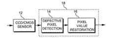
- FIG. 1shows a simplified high-level block diagram of an image processing unit that contains the main functional elements required to implement a blemish control algorithm, according to an embodiment of the present invention
- FIG. 2shows a depiction of an array of monochrome sensor elements with an underlying pixel circled and the neighboring pixels shown in the shaded area;
- FIG. 3shows a depiction of an array of color sensor elements with the underlying green pixels circled and the neighboring green pixels shown in the shaded area;
- FIG. 4shows a depiction of an array of color sensor elements with the underlying blue pixels circled and the neighboring blue pixels shown in the shaded area;
- FIG. 5shows a depiction of an array of color sensor elements with the underlying red pixels circled and the neighboring red pixels shown in the shaded area;
- FIG. 6shows a simplified high-level block diagram detailing the defective pixel detection stage of FIG. 1;
- FIG. 7shows a depiction of linear extrapolation for one-dimensional data
- FIG. 8shows a simplified high-level block diagram detailing the pixel value restoration stage of FIG. 1;
- FIG. 9shows a depiction of four possible feature lines passing through an underlying green pixel
- FIG. 10shows a depiction of four possible feature lines passing through an underlying blue pixel
- FIG. 11shows a depiction of four possible feature lines passing through an underlying red pixel
- FIG. 12shows a depiction of spatially adaptive interpolation along the direction of detected line or edge.
- FIG. 1shows a simplified high-level block diagram of an image processing unit 18 , also referred to as an intelligent control circuit, that contains the main functional elements required to implement a blemish control algorithm, according to embodiments of the present invention.
- Image processing unit 18includes a defective pixel detection stage 14 and a pixel value restoration stage 16 .
- An output from a CCD/CMOS sensor device 12feeds into image processing unit 18 .
- Image processing unit 18can operate with a CCD/CMOS sensor device in real-time, i.e., each time the CCD/CMOS feeds a new image to image processing unit 18 . This means that image processing unit 18 can operate in the field well after such a sensor has been manufactured and placed into products.
- defective pixel detection stage 14examines each pixel and its surrounding pixels, also referred to as neighboring pixels. Defective pixel detection stage 14 then determines whether each underlying pixel is defective. Defective pixel detection stage 14 can apply three tests to determine the type defect, e.g., whether the pixel is stuck low, stuck high, or abnormally sensitive, one test for each type of defect. If a defect is found, pixel value restoration stage 16 detects whether a line or an edge feature passes through the underlying pixel. Pixel value restoration stage 16 then replaces any defective pixel to a proper value, also referred to as a restoration value. This restoration value is derived from the neighboring pixels. These steps are described in more detail below.
- FIG. 2shows a depiction of an array of monochrome sensor elements with an underlying pixel circled and the neighboring pixels shown in the shaded area.
- the pixelsare for a monochrome sensor.
- the neighboring pixelsare divided into at least two groups, or tiers.
- the pixels in the surrounding areaare divided into two tiers N 1 and N 2 .
- Tier N 1includes the pixels immediately surrounding the underlying pixel.
- Tier N 2includes the pixels of tier N 1 and the pixels immediately surrounding tier N 1 .
- the present inventionis not limited to two tiers.
- the shape of the tierswill vary depending on the specific application. For instance, the tiers need not be rectangular. A diamond shaped area is also a reasonable choice for the surrounding area.
- FIG. 3shows a depiction of an array of color sensor elements with the underlying green pixels circled and the neighboring green pixels shown in the shaded area.
- the neighboring pixelsform a diamond shape.
- the size of the surrounding areacan vary depending on the specific application. A smaller area that only includes eight of the immediate pixels could be a reasonable choice.
- the pixelscan be allocated to different tiers in a variety of ways depending on the specific application.
- embodiments of the blemish control algorithmcan adapt to various patterns. For example, it can be applied to the Bayer pattern which is typically used for color CCD/CMOS sensors.
- the Bayer patternis widely used and is well known in the art. It is disclosed in U.S. Pat. No. 3,971,065, issued to B. E. Bayer. According to the pattern, the RGB color elements form a checker board pattern.
- FIG. 4shows a depiction of an array of color sensor elements with the underlying blue pixels circled and the neighboring blue pixels shown in the shaded area.
- FIG. 5shows a depiction of an array of color sensor elements with the underlying red pixels circled and the neighboring red pixels shown in the shaded area.
- each groupis processed separately.
- the intelligent control circuitcompares the value of the underlying pixel to the values of a first group of neighboring pixels for a stuck high test and for a stuck low test, and compares the value of the underlying pixel to the values of a second group of neighboring pixels for a abnormal sensitivity test.
- the blemish algorithmprocesses the pixels of tier N 1 first. If a defect is found, the underlying pixel is then processed by the pixel value restoration stage (described below). If no defect is found, the blemish algorithm then processes the pixels of tier N 2 .
- This specific orderis rather efficient because tier N 1 has fewer pixels than does tier N 2 making the processing faster.
- the stuck high and stuck low testsare applied to the pixels of tier N 1 and the abnormally sensitive test is applied to the pixels of tier N 2 .
- the specific order and stepswill depend on the application. In light of the present invention, one of ordinary skill in the art would recognize many other variations, modifications, and alternatives. For example, in other embodiments, both tiers could be processed for detection of a first type of defect before any tier is processed for a second type of defect. In yet other embodiments, for example, tiers N 1 and N 2 could be processes in parallel.
- FIG. 6shows a simplified high-level block diagram detailing the defective pixel detection 14 stage of FIG. 1 (labeled 120 in FIG. 6).
- Defective pixel detection stage 120couples to line buffers 112 .
- Line buffers 112serve as a temporary holding place for the lines around an underlying pixel. For the example, in FIG. 2, a total of five line buffers would be required. In FIG. 3, a total of nine line buffers would be required. In FIGS. 4 and 5, a total of five line buffers would be required.
- Defective pixel detection stage 120includes three processing stages: a white pixel detection stage 114 , a dark pixel detection stage 116 , and an abnormal sensitivity pixel detection stage 118 .
- the three processing stagesare shown in a tandem arrangement. They can, however, be in other arrangements, such as in a parallel arrangement, where a more efficient for hardware implementation such as a logic OR circuit can be used to combine the three results.
- each underlying pixelis tested for each type of defect.
- each underlying pixelis tested in the following order: stuck high, stuck low, and then abnormal sensitivity.
- the order of coursecan vary depending on the specific application. For example, another order of testing could be to first test for a stuck low defect, then a stuck high defect, then an abnormal sensitivity defect. Other orders of testing might be appropriate for some applications depending on the specific application.
- FIG. 6is merely an example and should not limit the scope of the claims herein.
- one of ordinary skill in the artwould recognize many other variations, modifications, and alternatives.
- the described system and methodcan be implemented in a multitude of different forms (i.e., software, hardware, or a combination of both) in a variety of systems.
- FIG. 7shows a depiction of linear extrapolation for one-dimensional data.
- the white pixel detection stage 114compares the value Ip of the underlying pixel with a threshold value White_Thresh. If I p >White_Thresh, the white pixel detection stage 114 performs the following calculation:
- Min_Diffmin(
- Min_Diffis then compared with a threshold value, white_Diff_Thresh. If
- the underlying pixelis declared to be a white pixel.
- the dark pixel detection stage 116compares the value I p of the underlying pixel with a threshold value Dark_Thresh. If I p ⁇ Dark_Thresh, the dark pixel detection stage 116 performs the following calculation:
- Min_Diffmin(
- Min_Diffis then compared with a threshold value, Dark_Diff_Thresh. If
- the underlying pixelis declared to be a dark pixel.
- the abnormal sensitivity pixel detection stage 118uses an extrapolation method to compare the underlying pixel value and the projected value. If the underlying pixel value varies from the projected value beyond a certain percentage, the underlying pixel is declared to be an abnormal pixel.
- a simple linear extrapolationis illustrated in FIG. 7. Let I A , I B , and I P be the pixel values for A, B, and P respectively.
- the projected value, Î P based on A and B using the linear extrapolation methodis:
- pixelsare determined whether they are defective or not. Pixels determined to be defective, they undergo pixel value restoration stage 16 (FIG. 1). Normal pixels bypass pixel value restoration stage 16 .
- FIG. 8shows a simplified high-level block diagram detailing the pixel value restoration stage 16 of FIG. 1.
- the pixel value restoration stagecouples to line buffers 122 .
- Line buffers 122serve as a temporary holding place for the lines around an underlying pixel.
- the pixel value restoration stageincludes a spatially adaptive interpolation stage 124 and line-edge feature detection stage 126 . Stages 124 and 126 involve the neighboring pixels, i.e., the pixels surrounding an underlying pixel. Line buffers 122 are thus required.
- Line buffers 122(as well as line buffers 112 of FIG. 6) can share the same memory.
- the intelligent control circuitapplies a spatially adaptive interpolation which involves either a one- or two-dimensional interpolation depending on whether or not a line or an edge feature passes through the underlying pixel, respectively.
- a spatially adaptive interpolationit must first be known whether a line or edge feature passes through the underlying pixel. There are some known techniques for detecting lines and edges, see Digital Image Processing, by R. C. Gonzalez and R. E. Woods, Addison-Wesley:Reading, Mass., 1992. If no line or edge feature is detected, the underlying pixel is likely in a smooth area. A regular two-dimensional linear interpolation would be sufficient. Regular (two-dimensional) image interpolation performs adequately for smooth areas. However, it often softens or smears sharp edges.
- a line-edge feature algorithmTo determine whether a line or edge feature passes through an underlying pixel, a line-edge feature algorithm, according to the present invention is invoked.
- one-dimensional interpolationis applied on the 4 neighboring pixels along the diagonal direction where a line or edge feature is detected.
- a properly designed algorithm for defective-pixel detectionwill lead to a small percentage of pixels being classified as defective. The majority of the pixels will not be affective by subsequent interpolation. Among the small percentage of pixels classified as defective, some of them might be misclassified. Nevertheless, the spatially adaptive interpolation (described below) should have little inadvertent effect. As a matter of fact, spatially adaptive interpolation can even enhance the picture quality.
- FIGS. 9, 10 and 11each show a depiction of four possible feature lines passing through an underlying green pixel, blue pixel and red pixel, respectively.
- a technique using a 5 ⁇ 5 maskis adopted. The line and edge features in four different orientations, as shown in FIGS. 9, 10 and 11 for green, blue and red pixels respectively, are tested.
- FIG. 12shows a depiction of spatially adaptive interpolation along the direction of detected line or edge. If a line or edge feature is detected, a one-dimensional interpolation is applied along the direction of the detected line or edge. The actual direction will depend on the specific image texture around the underlying pixel. As a result, spatially adaptive interpolation of the present invention restores the values of defective pixels while preserving the sharpness of images. Moreover, spatially adaptive interpolation stage 124 minimizes potential artifacts caused by interpolation on normal pixels.
- embodiments of the present inventionprovide numerous advantages. Principally, they mitigate problems associated with defective pixels in an efficient and reliable manner without the prior knowledge of the locations and the number of defective pixels.
- Specific embodiments of the present inventionare presented above for purposes of illustration and description. The full description will enable others skilled in the art to best utilize and practice the invention in various embodiments and with various modifications suited to particular uses. After reading and understanding the present disclosure, many modifications, variations, alternatives, and equivalents will be apparent to a person skilled in the art and are intended to be within the scope of this invention.
- the described circuits and methodcan be implemented in a multitude of different forms such as software, hardware, or a combination of both in a variety of systems. Therefore, it is not intended to be exhaustive or to limit the invention to the specific embodiments described, but is intended to be accorded the widest scope consistent with the principles and novel features disclosed herein, and as defined by the following claims.
Landscapes
- Engineering & Computer Science (AREA)
- Multimedia (AREA)
- Signal Processing (AREA)
- Transforming Light Signals Into Electric Signals (AREA)
- Color Television Image Signal Generators (AREA)
Abstract
Description
- 1. Field of the Invention[0001]
- The invention relates to the field of digital image processing and more specifically to blemish control in solid-state CCD/CMOS sensors that are subject to pixel defects.[0002]
- 2. Description Relative to the Prior Art[0003]
- Pixel defects in solid-state sensors such as CCD/CMOS sensors have been a common problem. The output from a CCD/CMOS sensor is subject to artifacts due to bad pixels. The visual effect of bad pixels can be very annoying as bad pixels manifest as black, white or gray dots in captured images. With sensor sizes increasing into the mega-pixel range, pixel defects are almost inevitable. Because it is very hard to produce defect-free sensors, it has been common practice for CCD/CMOS sensor manufacturers to market sensors with a small amount of defective pixels. These slightly defective sensors are often shipped with a record listing the locations of defective pixels.[0004]
- Sensors with a slight defect might be tolerable for some applications if care is taken to mitigate the effect of impairment. A common solution to mitigate the effect of pixel defects involves the registration of the bad pixel locations before the product is shipped and involves an algorithm to produce the proper pixel value for the corresponding bad pixels of the captured image. For example, Kodak, a sensor manufacturer, is marketing its sensors with various defect classes ranging from defect free to some point defects, cluster defects and column defects. Because the locations of bad pixels are random, a record of these locations must be kept with each individual device. Usually, the record is transferred to non-volatile memory in the sensor device. If the record is lost, however, the sensor device must be re-tested to obtain the locations of the bad pixels. Once the locations of the bad pixels are known, the corresponding pixel values should be replaced by values estimated from surrounding pixel values. Interpolation can be used to obtain the estimated values.[0005]
- Pixel defects can be classified in a variety of ways. According to one model, there are three types of pixel defects: stuck high, stuck low and abnormal sensitivity. When a pixel is stuck high (white pixel), its output is always very high regardless the input light intensity. When a pixel is stuck low (dark pixel), its output is always very low regardless of the input light intensity. The pixel subject to abnormal sensitivity produces an output level different from (higher or lower than) the normal pixels by a certain amount. To further illustrate, a pixel with the stuck high defect manifests itself as a very noticeable artifact (bright spot in a gray or dark area), which is most visually objectionable in a gray or dark area, particularly in a monochrome sensor. A pixel with stuck-low defect also produces a noticeable artifact (dark spot in a gray or bright area). A pixel with the abnormal-sensitivity defect is relatively more tolerable.[0006]
- Another traditional method of dealing with the defective pixels involves a defect table with predetermined locations of the defective pixels. A description of this method can be found in US Pat. No. 5,008,739, “Real-Time Digital Processor for Producing Full Resolution Color Signals from a Multi-Color Inage Sensor,” by Hibbard. In that disclosure, a defect concealment circuit is incorporated to estimate the values for defective pixels, the locations of which are predetermined and placed in a defect table (column 6, line 39).[0007]
- Another existing system to cope with the bad sensor pixels involves the application of a sequence of random test pictures. After each test picture is captured, each pixel of the sensor is compared to its neighboring pixels. Applying a function (see below), statistical data is collected to determine whether a pixel is defective. The probability of finding pixel defects increases as more test pictures are used. This method was developed by Y-P Tan and T. Acharya. This system is described in more detail in “A Robust Sequential Approach for the Detection of Defective Pixels in an Image Sensor,” published in Proceedings of IEEE Conference on Acoustics, Speech and Signal Processing, vol. 4, pp. 2239-2242, March 1999. A minimum neighboring pixel difference (MND) is calculated as:[0008]
- y(i,j)=min{|I(i,j)−I(m,n)|} for (m,n)∈G(i,j)
- where G(i,j) denotes the locations of the pixels within the neighboring support around pixel (i,j). I(i,j) is the output of pixel (i,j), and I(m,n) is the output pixel at (m,n). They examine the conditional probability density function p(y/z), where z is the pixel value from the neighborhood of (i,j) that results in the MND for the underlying pixel y. The conditional probability density function exhibits very distinctive characteristics between a normal pixel and a defective pixel. When enough statistical data is collected for each pixel location, a fairly accurate decision can be made as to whether an underlying pixel has a defect, and the type of defect if it is defective. Based on simulation, they concluded that accurate defect detection could be made with a training process where sequence of 8 random test pictures is applied to the function described above. Though the method can result in accurate defect detection, it relies on the training process to form the conditional probability density function. This process may not be desirable.[0009]
- Another method to alleviate the effect of defective pixels involves applying signal processing to every pixel. Proper pixel values are extrapolated from the values of neighboring pixels. The method is applied globally to all pixels whether defective or not. This method was developed by B. Dierickx and G. Meynants in “Missing Pixel Correction Algorithm for Image Sensor,” published in Proceedings of SPIE, vol. 3410, pp. 200-203, May 1998. The assumption is that an image projected through a lens or any other optical system is never perfectly sharp. Even with ideal lenses, a star image, for example, would not be projected on a single pixel. The point-like source of the star would be smeared out over a central pixel and a few neighbors. To correct the possible defective pixel, they examine 4 pixels surrounding an underlying pixel (one-dimensional processing). They form an extrapolated value for the underlying pixel from the 2 pixels on the left and the 2 pixels on the right.[0010]
- The upper bound, C[0011]max, for the underlying pixel is defined as the maximum value among the 2 extrapolated values and the two immediate neighboring pixel values. The lower bound, Cmin, for the underlying pixel is defined as the minimum value among the 2 extrapolated values and the two immediate neighboring pixel values. The final corrected value for the underlying pixel is the median of Cmax, Cmin, and the original underlying pixel value. The signal processing is applied to every pixel whether it is defective or not. Though the method does a fairly good job alleviating the effect of defective pixels, some subtle features, however, may be altered inadvertently. This occurs because even all pixels are fixed, even good pixels.
- A few US Patents granted in recent years relate to missing pixel processing for color image sensors. These patents, however, deal with an issue very different from the present invention. For example, U.S. Pat. Nos. 6,181,376 and 6,188,804 are directed to a full reconstruction of a sampled image which has missing information. In this case, the sensor does not provide full resolution samples. One such example is the Bayer pattern (RGB sampling pattern) where each line contains either R-G pixels or G-B pixels. The G pixel pattern thus represents 50% of the total pixels and each of the R and B pixels represent 25% of the total pixels. These two patents address the method of interpolating the values for the missing color pixels.[0012]
- If the locations of defective pixels are known, a simple interpolation would generally do a decent job. In such a scenario, when a slightly defective sensor is incorporated into an imaging system, a simple pixel interpolation can be applied to the defective locations. This simple method can effectively reduce the artifacts caused by bad pixels. However, a defective pixel detection algorithm can result in false detections where a normal pixel is classified as a defective pixel. Moreover, the probability of false detections increases as sensor sizes increase.[0013]
- A need therefore remains for an image processing method and apparatus that detects and identifies pixel defects without prior knowledge of such defects and restores the values of defective pixels in a manner that is time efficient, simple, and reliable. A need also remains for a method and apparatus that minimizes the occurrence of false detections.[0014]
- An intelligent control circuit for pixel defects in a sensor, the control circuit including a defective pixel detection circuit for detecting whether an underlying pixel is defective; and a pixel value restoration circuit for replacing the value of the underlying pixel, if defective, with a restoration value derived from the values of neighboring pixels; wherein the control circuit operates in real-time.[0015]
- The intelligent control circuit applies at least one of three tests to determine whether an underlying pixel has one of three types of defects: stuck high, stuck low and abnormal sensitivity. In one embodiment, the intelligent control circuit compares the value of the underlying pixel to the values of a first group of neighboring pixels for a stuck high test and for a stuck low test, and compares the value of the underlying pixel to the values of a second group of neighboring pixels for a abnormal sensitivity test. In one embodiment, the first group includes the pixels immediately surrounding the underlying pixel, and the second group includes the pixels immediately surrounding and including the first group. If a defect is found, the intelligent control circuit detects whether a line or an edge feature passes through the underlying pixel. The intelligent control circuit then replaces the value of the underlying pixel with a restoration value that is derived from the neighboring pixels. To derive the restoration value, the intelligent control circuit applies a spatially adaptive interpolation which involves either a one- or two-dimensional interpolation depending on whether or not a line or an edge feature passes through the underlying pixel, respectively.[0016]
- Embodiments of the present invention achieve their purposes and benefits in the context of known circuit technology and known techniques in the electronic arts. Further understanding, however, of the nature, objects, features, and advantages of the present invention is realized by reference to the latter portions of the specification, accompanying drawings, and appended claims. Other objects, features, and advantages of the present invention will become apparent upon consideration of the following detailed description, accompanying drawings, and appended claims.[0017]
- FIG. 1 shows a simplified high-level block diagram of an image processing unit that contains the main functional elements required to implement a blemish control algorithm, according to an embodiment of the present invention;[0018]
- FIG. 2 shows a depiction of an array of monochrome sensor elements with an underlying pixel circled and the neighboring pixels shown in the shaded area;[0019]
- FIG. 3 shows a depiction of an array of color sensor elements with the underlying green pixels circled and the neighboring green pixels shown in the shaded area;[0020]
- FIG. 4 shows a depiction of an array of color sensor elements with the underlying blue pixels circled and the neighboring blue pixels shown in the shaded area;[0021]
- FIG. 5 shows a depiction of an array of color sensor elements with the underlying red pixels circled and the neighboring red pixels shown in the shaded area;[0022]
- FIG. 6 shows a simplified high-level block diagram detailing the defective pixel detection stage of FIG. 1;[0023]
- FIG. 7 shows a depiction of linear extrapolation for one-dimensional data;[0024]
- FIG. 8 shows a simplified high-level block diagram detailing the pixel value restoration stage of FIG. 1;[0025]
- FIG. 9 shows a depiction of four possible feature lines passing through an underlying green pixel;[0026]
- FIG. 10 shows a depiction of four possible feature lines passing through an underlying blue pixel;[0027]
- FIG. 11 shows a depiction of four possible feature lines passing through an underlying red pixel; and[0028]
- FIG. 12 shows a depiction of spatially adaptive interpolation along the direction of detected line or edge.[0029]
- With reference to the drawings, embodiments of an image processing method and apparatus, according to the present invention, is described below.[0030]
- FIG. 1 shows a simplified high-level block diagram of an[0031]
image processing unit 18, also referred to as an intelligent control circuit, that contains the main functional elements required to implement a blemish control algorithm, according to embodiments of the present invention.Image processing unit 18 includes a defectivepixel detection stage 14 and a pixelvalue restoration stage 16. An output from a CCD/CMOS sensor device 12 feeds intoimage processing unit 18.Image processing unit 18 can operate with a CCD/CMOS sensor device in real-time, i.e., each time the CCD/CMOS feeds a new image toimage processing unit 18. This means thatimage processing unit 18 can operate in the field well after such a sensor has been manufactured and placed into products. - In operation, defective[0032]
pixel detection stage 14 examines each pixel and its surrounding pixels, also referred to as neighboring pixels. Defectivepixel detection stage 14 then determines whether each underlying pixel is defective. Defectivepixel detection stage 14 can apply three tests to determine the type defect, e.g., whether the pixel is stuck low, stuck high, or abnormally sensitive, one test for each type of defect. If a defect is found, pixelvalue restoration stage 16 detects whether a line or an edge feature passes through the underlying pixel. Pixelvalue restoration stage 16 then replaces any defective pixel to a proper value, also referred to as a restoration value. This restoration value is derived from the neighboring pixels. These steps are described in more detail below. - FIG. 2 shows a depiction of an array of monochrome sensor elements with an underlying pixel circled and the neighboring pixels shown in the shaded area. In this particular depiction, the pixels are for a monochrome sensor. In some embodiments, the neighboring pixels are divided into at least two groups, or tiers. Referring still to FIG. 2, the pixels in the surrounding area are divided into two tiers N[0033]1 and N2. Tier N1 includes the pixels immediately surrounding the underlying pixel. Tier N2 includes the pixels of tier N1 and the pixels immediately surrounding tier N1. The present invention is not limited to two tiers. For example, there could be a third tier that includes pixels immediately surrounding tier N2, and so on. Moreover, the shape of the tiers will vary depending on the specific application. For instance, the tiers need not be rectangular. A diamond shaped area is also a reasonable choice for the surrounding area.
- FIG. 3 shows a depiction of an array of color sensor elements with the underlying green pixels circled and the neighboring green pixels shown in the shaded area. Here, the neighboring pixels form a diamond shape. Moreover, the size of the surrounding area can vary depending on the specific application. A smaller area that only includes eight of the immediate pixels could be a reasonable choice.[0034]
- According to the present invention, the pixels can be allocated to different tiers in a variety of ways depending on the specific application. Moreover, embodiments of the blemish control algorithm can adapt to various patterns. For example, it can be applied to the Bayer pattern which is typically used for color CCD/CMOS sensors. The Bayer pattern is widely used and is well known in the art. It is disclosed in U.S. Pat. No. 3,971,065, issued to B. E. Bayer. According to the pattern, the RGB color elements form a checker board pattern.[0035]
- FIG. 4 shows a depiction of an array of color sensor elements with the underlying blue pixels circled and the neighboring blue pixels shown in the shaded area. FIG. 5 shows a depiction of an array of color sensor elements with the underlying red pixels circled and the neighboring red pixels shown in the shaded area. It is to be understood that the shape, size, and pattern of the tiers described are merely examples and should not limit the scope of the claims herein. In light of the present invention, one of ordinary skill in the art would recognize many other variations, modifications, and alternatives.[0036]
- When determining whether an underlying pixel is defective, each group is processed separately. The intelligent control circuit compares the value of the underlying pixel to the values of a first group of neighboring pixels for a stuck high test and for a stuck low test, and compares the value of the underlying pixel to the values of a second group of neighboring pixels for a abnormal sensitivity test.[0037]
- In one embodiment, the blemish algorithm processes the pixels of tier N[0038]1 first. If a defect is found, the underlying pixel is then processed by the pixel value restoration stage (described below). If no defect is found, the blemish algorithm then processes the pixels of tier N2. This specific order is rather efficient because tier N1 has fewer pixels than does tier N2 making the processing faster. Also, in some embodiments, the stuck high and stuck low tests are applied to the pixels of tier N1 and the abnormally sensitive test is applied to the pixels of tier N2. The specific order and steps will depend on the application. In light of the present invention, one of ordinary skill in the art would recognize many other variations, modifications, and alternatives. For example, in other embodiments, both tiers could be processed for detection of a first type of defect before any tier is processed for a second type of defect. In yet other embodiments, for example, tiers N1 and N2 could be processes in parallel.
- FIG. 6 shows a simplified high-level block diagram detailing the[0039]
defective pixel detection 14 stage of FIG. 1 (labeled120 in FIG. 6). Defectivepixel detection stage 120 couples to line buffers112. Line buffers112 serve as a temporary holding place for the lines around an underlying pixel. For the example, in FIG. 2, a total of five line buffers would be required. In FIG. 3, a total of nine line buffers would be required. In FIGS. 4 and 5, a total of five line buffers would be required. - Defective[0040]
pixel detection stage 120 includes three processing stages: a whitepixel detection stage 114, a darkpixel detection stage 116, and an abnormal sensitivitypixel detection stage 118. In the specific embodiment of FIG. 6, the three processing stages are shown in a tandem arrangement. They can, however, be in other arrangements, such as in a parallel arrangement, where a more efficient for hardware implementation such as a logic OR circuit can be used to combine the three results. - In operation, each underlying pixel is tested for each type of defect. In some embodiments, each underlying pixel is tested in the following order: stuck high, stuck low, and then abnormal sensitivity. The order of course can vary depending on the specific application. For example, another order of testing could be to first test for a stuck low defect, then a stuck high defect, then an abnormal sensitivity defect. Other orders of testing might be appropriate for some applications depending on the specific application.[0041]
- It is to be understood that the implementation of FIG. 6 is merely an example and should not limit the scope of the claims herein. In light of the present invention, one of ordinary skill in the art would recognize many other variations, modifications, and alternatives. Also, the described system and method can be implemented in a multitude of different forms (i.e., software, hardware, or a combination of both) in a variety of systems.[0042]
- FIG. 7 shows a depiction of linear extrapolation for one-dimensional data. The white[0043]
pixel detection stage 114 compares the value Ip of the underlying pixel with a threshold value White_Thresh. If Ip>White_Thresh, the whitepixel detection stage 114 performs the following calculation: - Min_Diff=min(|Ip−I(x)|) for allx∈
N 1 - The Min_Diff is then compared with a threshold value, white_Diff_Thresh. If[0044]
- Min_Diff>White_Diff_Thresh,
- the underlying pixel is declared to be a white pixel.[0045]
- If the underlying pixel is not a white pixel, the dark pixel detection is performed. The dark[0046]
pixel detection stage 116 compares the value Ipof the underlying pixel with a threshold value Dark_Thresh. If Ip<Dark_Thresh, the darkpixel detection stage 116 performs the following calculation: - Min_Diff=min(|Ip−I(x)|) for allx∈
N 1 - The Min_Diff is then compared with a threshold value, Dark_Diff_Thresh. If[0047]
- Min_Diff>Dark_Diff_Thresh
- the underlying pixel is declared to be a dark pixel. The abnormal sensitivity[0048]
pixel detection stage 118 uses an extrapolation method to compare the underlying pixel value and the projected value. If the underlying pixel value varies from the projected value beyond a certain percentage, the underlying pixel is declared to be an abnormal pixel. For the one-dimensional case, a simple linear extrapolation is illustrated in FIG. 7. Let IA, IB, and IPbe the pixel values for A, B, and P respectively. The projected value, ÎPbased on A and B using the linear extrapolation method is: - ÎP=2IB−IA.
- If (|ÎP−IP|/ÎP)>Thresh_AS, the underlying pixel is declared as an abnormal sensitivity pixel, where Thresh_AS is the threshold value.[0050]
- At the output of the defective[0051]
pixel detection stage 120, all pixels are determined whether they are defective or not. Pixels determined to be defective, they undergo pixel value restoration stage16 (FIG. 1). Normal pixels bypass pixelvalue restoration stage 16. - FIG. 8 shows a simplified high-level block diagram detailing the pixel[0052]
value restoration stage 16 of FIG. 1. The pixel value restoration stage couples to line buffers122. Line buffers122 serve as a temporary holding place for the lines around an underlying pixel. The pixel value restoration stage includes a spatiallyadaptive interpolation stage 124 and line-edgefeature detection stage 126.Stages - Generally, to derive a restoration value, the intelligent control circuit applies a spatially adaptive interpolation which involves either a one- or two-dimensional interpolation depending on whether or not a line or an edge feature passes through the underlying pixel, respectively. To apply a spatially adaptive interpolation, it must first be known whether a line or edge feature passes through the underlying pixel. There are some known techniques for detecting lines and edges, see[0053]Digital Image Processing,by R. C. Gonzalez and R. E. Woods, Addison-Wesley:Reading, Mass., 1992. If no line or edge feature is detected, the underlying pixel is likely in a smooth area. A regular two-dimensional linear interpolation would be sufficient. Regular (two-dimensional) image interpolation performs adequately for smooth areas. However, it often softens or smears sharp edges.
- To determine whether a line or edge feature passes through an underlying pixel, a line-edge feature algorithm, according to the present invention is invoked. In a specific embodiment, one-dimensional interpolation is applied on the 4 neighboring pixels along the diagonal direction where a line or edge feature is detected. A properly designed algorithm for defective-pixel detection will lead to a small percentage of pixels being classified as defective. The majority of the pixels will not be affective by subsequent interpolation. Among the small percentage of pixels classified as defective, some of them might be misclassified. Nevertheless, the spatially adaptive interpolation (described below) should have little inadvertent effect. As a matter of fact, spatially adaptive interpolation can even enhance the picture quality.[0054]
- Once it is determined whether a line or edge feature passes through an underlying pixel, a spatially adaptive interpolation filter is then applied accordingly. FIGS. 9, 10 and[0055]11 each show a depiction of four possible feature lines passing through an underlying green pixel, blue pixel and red pixel, respectively. In some embodiments, a technique using a 5×5 mask is adopted. The line and edge features in four different orientations, as shown in FIGS. 9, 10 and11 for green, blue and red pixels respectively, are tested.
- FIG. 12 shows a depiction of spatially adaptive interpolation along the direction of detected line or edge. If a line or edge feature is detected, a one-dimensional interpolation is applied along the direction of the detected line or edge. The actual direction will depend on the specific image texture around the underlying pixel. As a result, spatially adaptive interpolation of the present invention restores the values of defective pixels while preserving the sharpness of images. Moreover, spatially[0056]
adaptive interpolation stage 124 minimizes potential artifacts caused by interpolation on normal pixels. - Conclusion[0057]
- In conclusion, it can be seen that embodiments of the present invention provide numerous advantages. Principally, they mitigate problems associated with defective pixels in an efficient and reliable manner without the prior knowledge of the locations and the number of defective pixels. Specific embodiments of the present invention are presented above for purposes of illustration and description. The full description will enable others skilled in the art to best utilize and practice the invention in various embodiments and with various modifications suited to particular uses. After reading and understanding the present disclosure, many modifications, variations, alternatives, and equivalents will be apparent to a person skilled in the art and are intended to be within the scope of this invention. Moreover, the described circuits and method can be implemented in a multitude of different forms such as software, hardware, or a combination of both in a variety of systems. Therefore, it is not intended to be exhaustive or to limit the invention to the specific embodiments described, but is intended to be accorded the widest scope consistent with the principles and novel features disclosed herein, and as defined by the following claims.[0058]

Claims (31)
Priority Applications (2)
| Application Number | Priority Date | Filing Date | Title |
|---|---|---|---|
| US09/884,284US6985180B2 (en) | 2001-06-19 | 2001-06-19 | Intelligent blemish control algorithm and apparatus |
| US11/212,372US7199824B2 (en) | 2001-06-19 | 2005-08-25 | Intelligent blemish control algorithm and apparatus |
Applications Claiming Priority (1)
| Application Number | Priority Date | Filing Date | Title |
|---|---|---|---|
| US09/884,284US6985180B2 (en) | 2001-06-19 | 2001-06-19 | Intelligent blemish control algorithm and apparatus |
Related Child Applications (1)
| Application Number | Title | Priority Date | Filing Date |
|---|---|---|---|
| US11/212,372ContinuationUS7199824B2 (en) | 2001-06-19 | 2005-08-25 | Intelligent blemish control algorithm and apparatus |
Publications (2)
| Publication Number | Publication Date |
|---|---|
| US20020196354A1true US20020196354A1 (en) | 2002-12-26 |
| US6985180B2 US6985180B2 (en) | 2006-01-10 |
Family
ID=25384315
Family Applications (2)
| Application Number | Title | Priority Date | Filing Date |
|---|---|---|---|
| US09/884,284Expired - LifetimeUS6985180B2 (en) | 2001-06-19 | 2001-06-19 | Intelligent blemish control algorithm and apparatus |
| US11/212,372Expired - LifetimeUS7199824B2 (en) | 2001-06-19 | 2005-08-25 | Intelligent blemish control algorithm and apparatus |
Family Applications After (1)
| Application Number | Title | Priority Date | Filing Date |
|---|---|---|---|
| US11/212,372Expired - LifetimeUS7199824B2 (en) | 2001-06-19 | 2005-08-25 | Intelligent blemish control algorithm and apparatus |
Country Status (1)
| Country | Link |
|---|---|
| US (2) | US6985180B2 (en) |
Cited By (40)
| Publication number | Priority date | Publication date | Assignee | Title |
|---|---|---|---|---|
| US20020191101A1 (en)* | 2001-05-31 | 2002-12-19 | Olympus Optical Co., Ltd. | Defective image compensation system and method |
| US20030086009A1 (en)* | 2001-09-24 | 2003-05-08 | Winbond Electronics Corporation | Processing method of image compensation for digital camera |
| US20040032516A1 (en)* | 2002-08-16 | 2004-02-19 | Ramakrishna Kakarala | Digital image system and method for combining demosaicing and bad pixel correction |
| US20040051798A1 (en)* | 2002-09-18 | 2004-03-18 | Ramakrishna Kakarala | Method for detecting and correcting defective pixels in a digital image sensor |
| US6763084B2 (en)* | 2000-11-24 | 2004-07-13 | Siemens Aktiengesellschaft | Method for operating an image system of an imaging medical examination device and medical examination device |
| EP1487194A3 (en)* | 2003-06-12 | 2005-01-05 | General Electric Company | Method of real-time correction of non-functioning pixels in digital radiography |
| US20050036045A1 (en)* | 2002-02-04 | 2005-02-17 | Oliver Fuchs | Method for checking functional reliability of an image sensor having a plurality of pixels |
| GB2410804A (en)* | 2004-02-07 | 2005-08-10 | Accuscene Corp Ltd | Image processor with light intensity modifying means |
| EP1583356A4 (en)* | 2002-12-27 | 2006-01-04 | Nikon Corp | Image processing device and image processing program |
| US20060012694A1 (en)* | 2002-12-24 | 2006-01-19 | Yutaka Yoneda | Pixel defect detecting/correcting device and pixel defect detecting/correcting method |
| US20060209199A1 (en)* | 2005-03-17 | 2006-09-21 | Yoshiko Tanaka | Pixel interpolation method |
| US20060238629A1 (en)* | 2005-04-25 | 2006-10-26 | Hidehiko Sato | Pixel defect correction device |
| US20060284862A1 (en)* | 2005-04-27 | 2006-12-21 | Samsung Electronics Co., Ltd. | Method and apparatus for processing bayer-pattern digital color video signal |
| US20070086674A1 (en)* | 2005-10-18 | 2007-04-19 | Ricoh Company, Ltd. | Method and apparatus for image processing capable of effectively reducing an image noise |
| US20070086672A1 (en)* | 2005-09-16 | 2007-04-19 | Zeng Gengsheng L | System and method for partitioned-image filtering |
| US20070177039A1 (en)* | 2006-02-02 | 2007-08-02 | Canon Kabushiki Kaisha | Image pickup apparatus |
| WO2007106898A1 (en)* | 2006-03-15 | 2007-09-20 | Qualcomm Incorporated | Processing of sensor values in imaging systems |
| US20070257866A1 (en)* | 2006-05-08 | 2007-11-08 | Eastman Kodak Company | Method and apparatus for defect correction in a display |
| US20070291142A1 (en)* | 2006-06-19 | 2007-12-20 | Mtekvision Co., Ltd. | Apparatus for processing dead pixel |
| US20080079826A1 (en)* | 2006-10-02 | 2008-04-03 | Mtekvision Co., Ltd. | Apparatus for processing dead pixel |
| EP2026563A1 (en)* | 2007-08-14 | 2009-02-18 | Deutsche Thomson OHG | System and method for detecting defective pixels |
| US20090066821A1 (en)* | 2007-09-07 | 2009-03-12 | Jeffrey Matthew Achong | Method And Apparatus For Interpolating Missing Colors In A Color Filter Array |
| US20100034481A1 (en)* | 2008-08-05 | 2010-02-11 | Qualcomm Incorporated | Bad pixel cluster detection |
| US20110102624A1 (en)* | 2009-11-02 | 2011-05-05 | Sony Corporation | Pixel defect correction device, imaging apparatus, pixel defect correction method, and program |
| US8174560B2 (en) | 2007-04-11 | 2012-05-08 | Red.Com, Inc. | Video camera |
| US8237830B2 (en)* | 2007-04-11 | 2012-08-07 | Red.Com, Inc. | Video camera |
| US20140340546A1 (en)* | 2013-05-17 | 2014-11-20 | Arnold & Richter Cine Technik Gmbh & Co. Betriebs Kg | Pixel correction method |
| US20150029364A1 (en)* | 2013-01-07 | 2015-01-29 | Altasens, Inc. | Dynamic, local edge preserving defect pixel correction for image sensors |
| EP2449525A4 (en)* | 2009-07-02 | 2015-06-24 | Scint X Ab | Reduction of noise caused by absorption of x-ray photons in pixelated image sensors |
| US20160142658A1 (en)* | 2014-11-17 | 2016-05-19 | Young Sung CHO | Method of removing a bad pixel from a pixel image generated by an image sensor, an image sensor using the method, and an application processor using the method |
| US20160342843A1 (en)* | 2015-05-22 | 2016-11-24 | Tektronix, Inc. | Anomalous pixel detection |
| US9521384B2 (en) | 2013-02-14 | 2016-12-13 | Red.Com, Inc. | Green average subtraction in image data |
| US20170064228A1 (en)* | 2015-08-31 | 2017-03-02 | Via Alliance Semiconductor Co., Ltd. | Methods for correcting bad pixels and apparatuses using the same |
| US20170301059A1 (en)* | 2016-04-15 | 2017-10-19 | Canon Kabushiki Kaisha | Device for performing image transformation processing and method thereof |
| EP3276937A4 (en)* | 2015-03-25 | 2018-09-05 | Olympus Corporation | Image processing device, image processing method, and program |
| US10926357B2 (en)* | 2017-04-12 | 2021-02-23 | Dpix, Llc | Method and functional architecture for inline repair of defective imaging arrays |
| US11503294B2 (en) | 2017-07-05 | 2022-11-15 | Red.Com, Llc | Video image data processing in electronic devices |
| US20240031696A1 (en)* | 2022-07-20 | 2024-01-25 | Gentex Corporation | Image processing for pixel correction |
| DE102023121216A1 (en)* | 2023-08-09 | 2025-02-13 | Basler Aktiengesellschaft | Method and device for correcting a value of a correction target pixel of an image of an electronic camera |
| US12272041B1 (en)* | 2024-01-31 | 2025-04-08 | Trieye Ltd. | Systems and methods for statistics-based defect pixel detection |
Families Citing this family (20)
| Publication number | Priority date | Publication date | Assignee | Title |
|---|---|---|---|---|
| JP4347721B2 (en)* | 2004-02-27 | 2009-10-21 | オリンパス株式会社 | Pixel defect detection apparatus and method, and imaging apparatus |
| US7313288B2 (en)* | 2005-04-20 | 2007-12-25 | Cypress Semiconductor Corporation | Defect pixel correction in an image sensor |
| US8009209B2 (en)* | 2005-09-30 | 2011-08-30 | Simon Fraser University | Methods and apparatus for detecting defects in imaging arrays by image analysis |
| US7710472B2 (en)* | 2006-05-01 | 2010-05-04 | Warner Bros. Entertainment Inc. | Detection and/or correction of suppressed signal defects in moving images |
| US20080158396A1 (en)* | 2006-08-07 | 2008-07-03 | Transchip, Inc. | Image Signal Processor For CMOS Image Sensors |
| JP2008048104A (en)* | 2006-08-14 | 2008-02-28 | Sony Corp | Imaging apparatus, defect correction circuit, and defect correction method |
| US7800661B2 (en)* | 2006-12-22 | 2010-09-21 | Qualcomm Incorporated | Programmable pattern matching device |
| JP4908289B2 (en)* | 2007-03-30 | 2012-04-04 | 富士フイルム株式会社 | Image processing apparatus, method, and program |
| US8885076B2 (en)* | 2007-03-30 | 2014-11-11 | Hewlett-Packard Development Company, L.P. | Camera sensor defect correction and noise reduction |
| JP4826546B2 (en)* | 2007-06-18 | 2011-11-30 | ソニー株式会社 | Image processing apparatus, image processing method, and program |
| US20090091642A1 (en)* | 2007-10-03 | 2009-04-09 | Winbond Electronics Corp. | Image defect correction system using directional detection |
| US8208044B2 (en) | 2008-09-18 | 2012-06-26 | Qualcomm Incorporated | Bad pixel cluster detection |
| US7974805B2 (en)* | 2008-10-14 | 2011-07-05 | ON Semiconductor Trading, Ltd | Image sensor and method |
| US8189080B2 (en)* | 2009-04-03 | 2012-05-29 | Sony Corporation | Orientation-based approach for forming a demosaiced image, and for color correcting and zooming the demosaiced image |
| JP5541718B2 (en)* | 2010-08-19 | 2014-07-09 | キヤノン株式会社 | Imaging device and defective pixel detection method thereof |
| JP5664255B2 (en)* | 2011-01-14 | 2015-02-04 | ソニー株式会社 | Image processing apparatus, image processing method, and program |
| EA016450B1 (en)* | 2011-09-30 | 2012-05-30 | Закрытое Акционерное Общество "Импульс" | Method for brightness correction of defective pixels of digital monochrome image |
| JP6071419B2 (en)* | 2012-10-25 | 2017-02-01 | キヤノン株式会社 | Image processing apparatus and image processing method |
| CN104935837B (en)* | 2015-06-10 | 2018-02-06 | 无锡英斯特微电子有限公司 | For optical imagery pointing device and the image processing method of optical video equipment |
| US10440299B2 (en)* | 2015-09-04 | 2019-10-08 | Apple Inc. | Correcting pixel defects based on defect history in an image processing pipeline |
Citations (11)
| Publication number | Priority date | Publication date | Assignee | Title |
|---|---|---|---|---|
| US4189751A (en)* | 1976-04-30 | 1980-02-19 | Sony Corporation | Solid state television camera with defect compensation to reduce noise |
| US5008739A (en)* | 1989-02-13 | 1991-04-16 | Eastman Kodak Company | Real-time digital processor for producing full resolution color signals from a multi-color image sensor |
| US5805216A (en)* | 1994-06-06 | 1998-09-08 | Matsushita Electric Industrial Co., Ltd. | Defective pixel correction circuit |
| US5920344A (en)* | 1995-03-28 | 1999-07-06 | Samsung Electronics Co., Ltd. | CCD camera defective pixel compensation using stored gain values |
| US5995675A (en)* | 1995-07-22 | 1999-11-30 | Lg Semicon Co., Ltd. | Defect compensator for solid-state image pickup device |
| US6181376B1 (en)* | 1997-10-14 | 2001-01-30 | Intel Corporation | Method of determining missing color values for pixels in a color filter array |
| US6188804B1 (en)* | 1998-05-18 | 2001-02-13 | Eastman Kodak Company | Reconstructing missing pixel information to provide a full output image |
| US6307393B1 (en)* | 1996-01-19 | 2001-10-23 | Sony Corporation | Device for detecting defects in solid-state image sensor |
| US20010052938A1 (en)* | 2000-06-20 | 2001-12-20 | Olympus Optical Co., Ltd | Color image processing apparatus |
| US20020158977A1 (en)* | 2001-02-19 | 2002-10-31 | Eastman Kodak Company | Correcting defects in a digital image caused by a pre-existing defect in a pixel of an image sensor |
| US6768513B1 (en)* | 1999-10-07 | 2004-07-27 | Sanyo Electric Co., Ltd. | Deficient pixel detection method and image signal processor |
Family Cites Families (8)
| Publication number | Priority date | Publication date | Assignee | Title |
|---|---|---|---|---|
| JPS61261974A (en)* | 1985-05-15 | 1986-11-20 | Hitachi Ltd | Detecting circuit for spot flaw of solid-state image pickup element |
| EP0496573B1 (en)* | 1991-01-24 | 1995-12-20 | Matsushita Electric Industrial Co., Ltd. | Pixel defect removing circuit for solid-state image pickup device |
| JP2882227B2 (en)* | 1993-01-06 | 1999-04-12 | 松下電器産業株式会社 | Pixel defect correction device |
| JPH06245148A (en)* | 1993-02-17 | 1994-09-02 | Matsushita Electric Ind Co Ltd | Pixel defect correction device |
| US6529622B1 (en)* | 1998-10-30 | 2003-03-04 | General Electric Company | Method and apparatus for identifying defective regions in a discrete pixel detector |
| US6724945B1 (en)* | 2000-05-24 | 2004-04-20 | Hewlett-Packard Development Company, L.P. | Correcting defect pixels in a digital image |
| US6965395B1 (en)* | 2000-09-12 | 2005-11-15 | Dialog Semiconductor Gmbh | Methods and systems for detecting defective imaging pixels and pixel values |
| US6741754B2 (en)* | 2001-02-19 | 2004-05-25 | Eastman Kodak Company | Correcting for defects in a digital image taken by an image sensor caused by pre-existing defects in two pixels in adjacent columns of an image sensor |
- 2001
- 2001-06-19USUS09/884,284patent/US6985180B2/ennot_activeExpired - Lifetime
- 2005
- 2005-08-25USUS11/212,372patent/US7199824B2/ennot_activeExpired - Lifetime
Patent Citations (11)
| Publication number | Priority date | Publication date | Assignee | Title |
|---|---|---|---|---|
| US4189751A (en)* | 1976-04-30 | 1980-02-19 | Sony Corporation | Solid state television camera with defect compensation to reduce noise |
| US5008739A (en)* | 1989-02-13 | 1991-04-16 | Eastman Kodak Company | Real-time digital processor for producing full resolution color signals from a multi-color image sensor |
| US5805216A (en)* | 1994-06-06 | 1998-09-08 | Matsushita Electric Industrial Co., Ltd. | Defective pixel correction circuit |
| US5920344A (en)* | 1995-03-28 | 1999-07-06 | Samsung Electronics Co., Ltd. | CCD camera defective pixel compensation using stored gain values |
| US5995675A (en)* | 1995-07-22 | 1999-11-30 | Lg Semicon Co., Ltd. | Defect compensator for solid-state image pickup device |
| US6307393B1 (en)* | 1996-01-19 | 2001-10-23 | Sony Corporation | Device for detecting defects in solid-state image sensor |
| US6181376B1 (en)* | 1997-10-14 | 2001-01-30 | Intel Corporation | Method of determining missing color values for pixels in a color filter array |
| US6188804B1 (en)* | 1998-05-18 | 2001-02-13 | Eastman Kodak Company | Reconstructing missing pixel information to provide a full output image |
| US6768513B1 (en)* | 1999-10-07 | 2004-07-27 | Sanyo Electric Co., Ltd. | Deficient pixel detection method and image signal processor |
| US20010052938A1 (en)* | 2000-06-20 | 2001-12-20 | Olympus Optical Co., Ltd | Color image processing apparatus |
| US20020158977A1 (en)* | 2001-02-19 | 2002-10-31 | Eastman Kodak Company | Correcting defects in a digital image caused by a pre-existing defect in a pixel of an image sensor |
Cited By (90)
| Publication number | Priority date | Publication date | Assignee | Title |
|---|---|---|---|---|
| US6763084B2 (en)* | 2000-11-24 | 2004-07-13 | Siemens Aktiengesellschaft | Method for operating an image system of an imaging medical examination device and medical examination device |
| US20020191101A1 (en)* | 2001-05-31 | 2002-12-19 | Olympus Optical Co., Ltd. | Defective image compensation system and method |
| US7250969B2 (en)* | 2001-05-31 | 2007-07-31 | Olympus Corporation | Defective image compensation system and method |
| US7084913B2 (en)* | 2001-09-24 | 2006-08-01 | Winbond Electronics Corp. | Processing method of image compensation for digital camera |
| US20030086009A1 (en)* | 2001-09-24 | 2003-05-08 | Winbond Electronics Corporation | Processing method of image compensation for digital camera |
| US20050036045A1 (en)* | 2002-02-04 | 2005-02-17 | Oliver Fuchs | Method for checking functional reliability of an image sensor having a plurality of pixels |
| US7872678B2 (en)* | 2002-02-04 | 2011-01-18 | Pilz Gmbh & Co. Kg | Method for checking functional reliability of an image sensor having a plurality of pixels |
| US20040032516A1 (en)* | 2002-08-16 | 2004-02-19 | Ramakrishna Kakarala | Digital image system and method for combining demosaicing and bad pixel correction |
| US7015961B2 (en)* | 2002-08-16 | 2006-03-21 | Ramakrishna Kakarala | Digital image system and method for combining demosaicing and bad pixel correction |
| US20040051798A1 (en)* | 2002-09-18 | 2004-03-18 | Ramakrishna Kakarala | Method for detecting and correcting defective pixels in a digital image sensor |
| US7283164B2 (en)* | 2002-09-18 | 2007-10-16 | Micron Technology, Inc. | Method for detecting and correcting defective pixels in a digital image sensor |
| US20060012694A1 (en)* | 2002-12-24 | 2006-01-19 | Yutaka Yoneda | Pixel defect detecting/correcting device and pixel defect detecting/correcting method |
| US7564491B2 (en)* | 2002-12-24 | 2009-07-21 | Sony Corporation | Pixel defect detecting/correcting device and pixel defect detecting/correcting method |
| US20100092103A1 (en)* | 2002-12-27 | 2010-04-15 | Nikon Corporation | Image processing apparatus and image processing program |
| US7853097B2 (en) | 2002-12-27 | 2010-12-14 | Nikon Corporation | Image processing apparatus and image processing program |
| US8031968B2 (en) | 2002-12-27 | 2011-10-04 | Nikon Corporation | Image processing apparatus and image processing program |
| US20060115177A1 (en)* | 2002-12-27 | 2006-06-01 | Nikon Corporation | Image processing device and image processing program |
| EP1583356A4 (en)* | 2002-12-27 | 2006-01-04 | Nikon Corp | Image processing device and image processing program |
| US8369651B2 (en) | 2002-12-27 | 2013-02-05 | Nikon Corporation | Image processing apparatus and image processing program |
| EP2461576A1 (en)* | 2002-12-27 | 2012-06-06 | Nikon Corporation | Image processing apparatus and image processing program |
| US7499599B2 (en) | 2003-06-12 | 2009-03-03 | General Electric Company | Method of real-time correction of non-functioning pixels in digital radiography |
| EP1487194A3 (en)* | 2003-06-12 | 2005-01-05 | General Electric Company | Method of real-time correction of non-functioning pixels in digital radiography |
| GB2410804A (en)* | 2004-02-07 | 2005-08-10 | Accuscene Corp Ltd | Image processor with light intensity modifying means |
| US20060209199A1 (en)* | 2005-03-17 | 2006-09-21 | Yoshiko Tanaka | Pixel interpolation method |
| US7453503B2 (en)* | 2005-03-17 | 2008-11-18 | Uniden Corporation | Pixel interpolation method |
| US8035702B2 (en)* | 2005-04-25 | 2011-10-11 | Eastman Kodak Company | Pixel defect correction device for line crawl |
| US20060238629A1 (en)* | 2005-04-25 | 2006-10-26 | Hidehiko Sato | Pixel defect correction device |
| US7671909B2 (en) | 2005-04-27 | 2010-03-02 | Samsung Electronics Co., Ltd. | Method and apparatus for processing Bayer-pattern digital color video signal |
| US20060284862A1 (en)* | 2005-04-27 | 2006-12-21 | Samsung Electronics Co., Ltd. | Method and apparatus for processing bayer-pattern digital color video signal |
| US20070086672A1 (en)* | 2005-09-16 | 2007-04-19 | Zeng Gengsheng L | System and method for partitioned-image filtering |
| US7983508B2 (en) | 2005-10-18 | 2011-07-19 | Ricoh Company, Ltd. | Method and apparatus for image processing capable of effectively reducing an image noise |
| US20070086674A1 (en)* | 2005-10-18 | 2007-04-19 | Ricoh Company, Ltd. | Method and apparatus for image processing capable of effectively reducing an image noise |
| EP1777940A3 (en)* | 2005-10-18 | 2009-07-29 | Ricoh Company, Ltd. | A method and apparatus for reducing an image noise |
| US20070177039A1 (en)* | 2006-02-02 | 2007-08-02 | Canon Kabushiki Kaisha | Image pickup apparatus |
| US7852383B2 (en)* | 2006-02-02 | 2010-12-14 | Canon Kabushiki Kaisha | Image pickup apparatus |
| US20070216786A1 (en)* | 2006-03-15 | 2007-09-20 | Szepo Robert Hung | Processing of sensor values in imaging systems |
| US7667747B2 (en) | 2006-03-15 | 2010-02-23 | Qualcomm Incorporated | Processing of sensor values in imaging systems |
| US20100182463A1 (en)* | 2006-03-15 | 2010-07-22 | Qualcomm Incorporated | Processing of sensor values in imaging systems |
| WO2007106898A1 (en)* | 2006-03-15 | 2007-09-20 | Qualcomm Incorporated | Processing of sensor values in imaging systems |
| US8077228B2 (en) | 2006-03-15 | 2011-12-13 | Qualcomm Incorporated | Processing of sensor values in imaging systems |
| US20070257866A1 (en)* | 2006-05-08 | 2007-11-08 | Eastman Kodak Company | Method and apparatus for defect correction in a display |
| US7676084B2 (en)* | 2006-06-19 | 2010-03-09 | Mtekvision Co., Ltd. | Apparatus for processing dead pixel |
| US20070291142A1 (en)* | 2006-06-19 | 2007-12-20 | Mtekvision Co., Ltd. | Apparatus for processing dead pixel |
| US20080079826A1 (en)* | 2006-10-02 | 2008-04-03 | Mtekvision Co., Ltd. | Apparatus for processing dead pixel |
| US7649555B2 (en)* | 2006-10-02 | 2010-01-19 | Mtekvision Co., Ltd. | Apparatus for processing dead pixel |
| US9245314B2 (en) | 2007-04-11 | 2016-01-26 | Red.Com, Inc. | Video camera |
| US9792672B2 (en) | 2007-04-11 | 2017-10-17 | Red.Com, Llc | Video capture devices and methods |
| US9436976B2 (en) | 2007-04-11 | 2016-09-06 | Red.Com, Inc. | Video camera |
| US8174560B2 (en) | 2007-04-11 | 2012-05-08 | Red.Com, Inc. | Video camera |
| US9596385B2 (en) | 2007-04-11 | 2017-03-14 | Red.Com, Inc. | Electronic apparatus |
| US8237830B2 (en)* | 2007-04-11 | 2012-08-07 | Red.Com, Inc. | Video camera |
| US8358357B2 (en) | 2007-04-11 | 2013-01-22 | Red.Com, Inc. | Video camera |
| US9787878B2 (en) | 2007-04-11 | 2017-10-10 | Red.Com, Llc | Video camera |
| US9230299B2 (en) | 2007-04-11 | 2016-01-05 | Red.Com, Inc. | Video camera |
| US8872933B2 (en) | 2007-04-11 | 2014-10-28 | Red.Com, Inc. | Video camera |
| US8878952B2 (en) | 2007-04-11 | 2014-11-04 | Red.Com, Inc. | Video camera |
| US9019393B2 (en) | 2007-04-11 | 2015-04-28 | Red.Com, Inc. | Video processing system and method |
| EP2026563A1 (en)* | 2007-08-14 | 2009-02-18 | Deutsche Thomson OHG | System and method for detecting defective pixels |
| US7825965B2 (en)* | 2007-09-07 | 2010-11-02 | Seiko Epson Corporation | Method and apparatus for interpolating missing colors in a color filter array |
| US20090066821A1 (en)* | 2007-09-07 | 2009-03-12 | Jeffrey Matthew Achong | Method And Apparatus For Interpolating Missing Colors In A Color Filter Array |
| US8971659B2 (en)* | 2008-08-05 | 2015-03-03 | Qualcomm Incorporated | Bad pixel cluster detection |
| US20100034481A1 (en)* | 2008-08-05 | 2010-02-11 | Qualcomm Incorporated | Bad pixel cluster detection |
| EP2449525A4 (en)* | 2009-07-02 | 2015-06-24 | Scint X Ab | Reduction of noise caused by absorption of x-ray photons in pixelated image sensors |
| US8576309B2 (en)* | 2009-11-02 | 2013-11-05 | Sony Corporation | Pixel defect correction device, imaging apparatus, pixel defect correction method, and program |
| US20110102624A1 (en)* | 2009-11-02 | 2011-05-05 | Sony Corporation | Pixel defect correction device, imaging apparatus, pixel defect correction method, and program |
| US20150029364A1 (en)* | 2013-01-07 | 2015-01-29 | Altasens, Inc. | Dynamic, local edge preserving defect pixel correction for image sensors |
| US9124832B2 (en)* | 2013-01-07 | 2015-09-01 | Altasens, Inc. | Dynamic, local edge preserving defect pixel correction for image sensors |
| US9521384B2 (en) | 2013-02-14 | 2016-12-13 | Red.Com, Inc. | Green average subtraction in image data |
| US10582168B2 (en) | 2013-02-14 | 2020-03-03 | Red.Com, Llc | Green image data processing |
| US9716866B2 (en) | 2013-02-14 | 2017-07-25 | Red.Com, Inc. | Green image data processing |
| US20140340546A1 (en)* | 2013-05-17 | 2014-11-20 | Arnold & Richter Cine Technik Gmbh & Co. Betriebs Kg | Pixel correction method |
| US9288408B2 (en)* | 2013-05-17 | 2016-03-15 | Arnold & Richter Cine Technik Gmbh & Co. Betriebs Kg | Pixel correction method |
| US20160142658A1 (en)* | 2014-11-17 | 2016-05-19 | Young Sung CHO | Method of removing a bad pixel from a pixel image generated by an image sensor, an image sensor using the method, and an application processor using the method |
| US9762827B2 (en)* | 2014-11-17 | 2017-09-12 | Samsung Electronics Co., Ltd. | Method of removing a bad pixel from a pixel image generated by an image sensor, an image sensor using the method, and an application processor using the method |
| EP3276937A4 (en)* | 2015-03-25 | 2018-09-05 | Olympus Corporation | Image processing device, image processing method, and program |
| US10025988B2 (en)* | 2015-05-22 | 2018-07-17 | Tektronix, Inc. | Anomalous pixel detection |
| US20160342843A1 (en)* | 2015-05-22 | 2016-11-24 | Tektronix, Inc. | Anomalous pixel detection |
| US9807324B2 (en)* | 2015-08-31 | 2017-10-31 | Via Alliance Semiconductor Co., Ltd. | Methods for correcting bad pixels and apparatuses using the same |
| US20170064228A1 (en)* | 2015-08-31 | 2017-03-02 | Via Alliance Semiconductor Co., Ltd. | Methods for correcting bad pixels and apparatuses using the same |
| US20170301059A1 (en)* | 2016-04-15 | 2017-10-19 | Canon Kabushiki Kaisha | Device for performing image transformation processing and method thereof |
| US10325345B2 (en)* | 2016-04-15 | 2019-06-18 | Canon Kabushiki Kaisha | Device for performing image transformation processing and method thereof |
| US10926357B2 (en)* | 2017-04-12 | 2021-02-23 | Dpix, Llc | Method and functional architecture for inline repair of defective imaging arrays |
| US11503294B2 (en) | 2017-07-05 | 2022-11-15 | Red.Com, Llc | Video image data processing in electronic devices |
| US11818351B2 (en) | 2017-07-05 | 2023-11-14 | Red.Com, Llc | Video image data processing in electronic devices |
| US12301806B2 (en) | 2017-07-05 | 2025-05-13 | RED Digital Cinema, Inc. | Video image data processing in electronic devices |
| US20240031696A1 (en)* | 2022-07-20 | 2024-01-25 | Gentex Corporation | Image processing for pixel correction |
| US12348885B2 (en)* | 2022-07-20 | 2025-07-01 | Gentex Corporation | Image processing for pixel correction |
| DE102023121216A1 (en)* | 2023-08-09 | 2025-02-13 | Basler Aktiengesellschaft | Method and device for correcting a value of a correction target pixel of an image of an electronic camera |
| DE102023121216B4 (en) | 2023-08-09 | 2025-03-13 | Basler Aktiengesellschaft | Method and apparatus for correcting a value of a correction target pixel of an image of an electronic camera |
| US12272041B1 (en)* | 2024-01-31 | 2025-04-08 | Trieye Ltd. | Systems and methods for statistics-based defect pixel detection |
Also Published As
| Publication number | Publication date |
|---|---|
| US20060012695A1 (en) | 2006-01-19 |
| US6985180B2 (en) | 2006-01-10 |
| US7199824B2 (en) | 2007-04-03 |
Similar Documents
| Publication | Publication Date | Title |
|---|---|---|
| US6985180B2 (en) | Intelligent blemish control algorithm and apparatus | |
| US8879869B2 (en) | Image defect map creation using batches of digital images | |
| EP1583356B1 (en) | Image processing device and image processing program | |
| US7536036B2 (en) | Method and apparatus for red-eye detection in an acquired digital image | |
| US6965395B1 (en) | Methods and systems for detecting defective imaging pixels and pixel values | |
| US7206461B2 (en) | Digital image acquisition and processing system | |
| EP1157544B1 (en) | Hi-speed deterministic approach in detecting defective pixels within an image sensor | |
| CN103369347B (en) | Camera blemish defects detection | |
| US7369712B2 (en) | Automated statistical self-calibrating detection and removal of blemishes in digital images based on multiple occurrences of dust in images | |
| US7310450B2 (en) | Method of detecting and correcting dust in digital images based on aura and shadow region analysis | |
| JP4243454B2 (en) | Brightness correction method, selective defect detection method, and recording medium on which these are recorded | |
| JP2006303491A (en) | Method of inspecting wafer | |
| JP6831934B2 (en) | Pixel sensor defect classification and correction method using color channel defect pixel information | |
| US7535501B1 (en) | Testing of digital cameras | |
| US6400468B1 (en) | Smoothing calibration files to improve reproduction of digitized images | |
| US20060067569A1 (en) | Image inspection device, image inspection method, and image inspection program | |
| KR101012626B1 (en) | Method and apparatus for defect pixel detection based on human vision system | |
| US12380548B2 (en) | Method and system of adaptably detecting dirt, occlusion and smudge on camera lens and image sensor | |
| JP2005140655A (en) | Method and apparatus for detecting spot defects | |
| JP4244046B2 (en) | Image processing method and image processing apparatus | |
| JP3015325B2 (en) | Streak inspection method and device | |
| KR100754969B1 (en) | Image inspecting apparatus, image inspecting method, and computer-readable storage medium | |
| JP4273835B2 (en) | Signal processing apparatus and electronic camera | |
| JPH08110307A (en) | Pattern inspection method | |
| JP2003091728A (en) | Detection method of image shading unevenness |
Legal Events
| Date | Code | Title | Description |
|---|---|---|---|
| AS | Assignment | Owner name:DIVIO, INC., CALIFORNIA Free format text:ASSIGNMENT OF ASSIGNORS INTEREST;ASSIGNORS:CHANG, MICHAEL;YEH, ALLAN;TZOU, KOU-HU;REEL/FRAME:011926/0384 Effective date:20010615 | |
| AS | Assignment | Owner name:ESS TECHNOLOGIES INTERNATIONAL, INC., CALIFORNIA Free format text:ASSIGNMENT OF ASSIGNORS INTEREST;ASSIGNOR:DIVIO, INC.;REEL/FRAME:015541/0116 Effective date:20040625 | |
| STCF | Information on status: patent grant | Free format text:PATENTED CASE | |
| CC | Certificate of correction | ||
| AS | Assignment | Owner name:IMPERIUM (IP) HOLDINGS, NEW YORK Free format text:ASSIGNMENT OF ASSIGNORS INTEREST;ASSIGNOR:ESS TECHNOLOGY, INC.;REEL/FRAME:021316/0252 Effective date:20080630 | |
| FPAY | Fee payment | Year of fee payment:4 | |
| REMI | Maintenance fee reminder mailed | ||
| FPAY | Fee payment | Year of fee payment:8 | |
| SULP | Surcharge for late payment | Year of fee payment:7 | |
| FEPP | Fee payment procedure | Free format text:MAINTENANCE FEE REMINDER MAILED (ORIGINAL EVENT CODE: REM.) | |
| FEPP | Fee payment procedure | Free format text:11.5 YR SURCHARGE- LATE PMT W/IN 6 MO, LARGE ENTITY (ORIGINAL EVENT CODE: M1556) | |
| MAFP | Maintenance fee payment | Free format text:PAYMENT OF MAINTENANCE FEE, 12TH YEAR, LARGE ENTITY (ORIGINAL EVENT CODE: M1553) Year of fee payment:12 | |
| AS | Assignment | Owner name:PICTOS TECHNOLOGIES INC., CALIFORNIA Free format text:CHANGE OF NAME;ASSIGNOR:IMPERIUM IP HOLDINGS (CAYMAN), LTD.;REEL/FRAME:056595/0208 Effective date:20180430 | |
| AS | Assignment | Owner name:RE SECURED NETWORKS LLC, TEXAS Free format text:ASSIGNMENT OF ASSIGNORS INTEREST;ASSIGNOR:PICTOS TECHNOLOGIES INC;REEL/FRAME:060801/0001 Effective date:20220706 |