US20020192975A1 - Dielectric layer forming method and devices formed therewith - Google Patents
Dielectric layer forming method and devices formed therewithDownload PDFInfo
- Publication number
- US20020192975A1 US20020192975A1US10/174,434US17443402AUS2002192975A1US 20020192975 A1US20020192975 A1US 20020192975A1US 17443402 AUS17443402 AUS 17443402AUS 2002192975 A1US2002192975 A1US 2002192975A1
- Authority
- US
- United States
- Prior art keywords
- layer
- dielectric layer
- hafnium
- metal
- forming
- Prior art date
- Legal status (The legal status is an assumption and is not a legal conclusion. Google has not performed a legal analysis and makes no representation as to the accuracy of the status listed.)
- Granted
Links
Images


Classifications
- H—ELECTRICITY
- H01—ELECTRIC ELEMENTS
- H01L—SEMICONDUCTOR DEVICES NOT COVERED BY CLASS H10
- H01L21/00—Processes or apparatus adapted for the manufacture or treatment of semiconductor or solid state devices or of parts thereof
- H01L21/02—Manufacture or treatment of semiconductor devices or of parts thereof
- H01L21/02104—Forming layers
- H01L21/02107—Forming insulating materials on a substrate
- H01L21/02109—Forming insulating materials on a substrate characterised by the type of layer, e.g. type of material, porous/non-porous, pre-cursors, mixtures or laminates
- H01L21/022—Forming insulating materials on a substrate characterised by the type of layer, e.g. type of material, porous/non-porous, pre-cursors, mixtures or laminates the layer being a laminate, i.e. composed of sublayers, e.g. stacks of alternating high-k metal oxides
- H—ELECTRICITY
- H01—ELECTRIC ELEMENTS
- H01L—SEMICONDUCTOR DEVICES NOT COVERED BY CLASS H10
- H01L21/00—Processes or apparatus adapted for the manufacture or treatment of semiconductor or solid state devices or of parts thereof
- H01L21/02—Manufacture or treatment of semiconductor devices or of parts thereof
- H01L21/02104—Forming layers
- H01L21/02107—Forming insulating materials on a substrate
- H01L21/02109—Forming insulating materials on a substrate characterised by the type of layer, e.g. type of material, porous/non-porous, pre-cursors, mixtures or laminates
- H01L21/02112—Forming insulating materials on a substrate characterised by the type of layer, e.g. type of material, porous/non-porous, pre-cursors, mixtures or laminates characterised by the material of the layer
- H01L21/02172—Forming insulating materials on a substrate characterised by the type of layer, e.g. type of material, porous/non-porous, pre-cursors, mixtures or laminates characterised by the material of the layer the material containing at least one metal element, e.g. metal oxides, metal nitrides, metal oxynitrides or metal carbides
- H01L21/02175—Forming insulating materials on a substrate characterised by the type of layer, e.g. type of material, porous/non-porous, pre-cursors, mixtures or laminates characterised by the material of the layer the material containing at least one metal element, e.g. metal oxides, metal nitrides, metal oxynitrides or metal carbides characterised by the metal
- H—ELECTRICITY
- H01—ELECTRIC ELEMENTS
- H01L—SEMICONDUCTOR DEVICES NOT COVERED BY CLASS H10
- H01L21/00—Processes or apparatus adapted for the manufacture or treatment of semiconductor or solid state devices or of parts thereof
- H01L21/02—Manufacture or treatment of semiconductor devices or of parts thereof
- H01L21/02104—Forming layers
- H01L21/02107—Forming insulating materials on a substrate
- H01L21/02225—Forming insulating materials on a substrate characterised by the process for the formation of the insulating layer
- H01L21/02227—Forming insulating materials on a substrate characterised by the process for the formation of the insulating layer formation by a process other than a deposition process
- H01L21/0223—Forming insulating materials on a substrate characterised by the process for the formation of the insulating layer formation by a process other than a deposition process formation by oxidation, e.g. oxidation of the substrate
- H01L21/02244—Forming insulating materials on a substrate characterised by the process for the formation of the insulating layer formation by a process other than a deposition process formation by oxidation, e.g. oxidation of the substrate of a metallic layer
- H—ELECTRICITY
- H01—ELECTRIC ELEMENTS
- H01L—SEMICONDUCTOR DEVICES NOT COVERED BY CLASS H10
- H01L21/00—Processes or apparatus adapted for the manufacture or treatment of semiconductor or solid state devices or of parts thereof
- H01L21/02—Manufacture or treatment of semiconductor devices or of parts thereof
- H01L21/04—Manufacture or treatment of semiconductor devices or of parts thereof the devices having potential barriers, e.g. a PN junction, depletion layer or carrier concentration layer
- H01L21/18—Manufacture or treatment of semiconductor devices or of parts thereof the devices having potential barriers, e.g. a PN junction, depletion layer or carrier concentration layer the devices having semiconductor bodies comprising elements of Group IV of the Periodic Table or AIIIBV compounds with or without impurities, e.g. doping materials
- H01L21/28—Manufacture of electrodes on semiconductor bodies using processes or apparatus not provided for in groups H01L21/20 - H01L21/268
- H01L21/28008—Making conductor-insulator-semiconductor electrodes
- H01L21/28017—Making conductor-insulator-semiconductor electrodes the insulator being formed after the semiconductor body, the semiconductor being silicon
- H01L21/28158—Making the insulator
- H01L21/28167—Making the insulator on single crystalline silicon, e.g. using a liquid, i.e. chemical oxidation
- H01L21/28185—Making the insulator on single crystalline silicon, e.g. using a liquid, i.e. chemical oxidation with a treatment, e.g. annealing, after the formation of the gate insulator and before the formation of the definitive gate conductor
- H—ELECTRICITY
- H01—ELECTRIC ELEMENTS
- H01L—SEMICONDUCTOR DEVICES NOT COVERED BY CLASS H10
- H01L21/00—Processes or apparatus adapted for the manufacture or treatment of semiconductor or solid state devices or of parts thereof
- H01L21/02—Manufacture or treatment of semiconductor devices or of parts thereof
- H01L21/04—Manufacture or treatment of semiconductor devices or of parts thereof the devices having potential barriers, e.g. a PN junction, depletion layer or carrier concentration layer
- H01L21/18—Manufacture or treatment of semiconductor devices or of parts thereof the devices having potential barriers, e.g. a PN junction, depletion layer or carrier concentration layer the devices having semiconductor bodies comprising elements of Group IV of the Periodic Table or AIIIBV compounds with or without impurities, e.g. doping materials
- H01L21/28—Manufacture of electrodes on semiconductor bodies using processes or apparatus not provided for in groups H01L21/20 - H01L21/268
- H01L21/28008—Making conductor-insulator-semiconductor electrodes
- H01L21/28017—Making conductor-insulator-semiconductor electrodes the insulator being formed after the semiconductor body, the semiconductor being silicon
- H01L21/28158—Making the insulator
- H01L21/28167—Making the insulator on single crystalline silicon, e.g. using a liquid, i.e. chemical oxidation
- H01L21/28194—Making the insulator on single crystalline silicon, e.g. using a liquid, i.e. chemical oxidation by deposition, e.g. evaporation, ALD, CVD, sputtering, laser deposition
- H—ELECTRICITY
- H01—ELECTRIC ELEMENTS
- H01L—SEMICONDUCTOR DEVICES NOT COVERED BY CLASS H10
- H01L21/00—Processes or apparatus adapted for the manufacture or treatment of semiconductor or solid state devices or of parts thereof
- H01L21/02—Manufacture or treatment of semiconductor devices or of parts thereof
- H01L21/04—Manufacture or treatment of semiconductor devices or of parts thereof the devices having potential barriers, e.g. a PN junction, depletion layer or carrier concentration layer
- H01L21/18—Manufacture or treatment of semiconductor devices or of parts thereof the devices having potential barriers, e.g. a PN junction, depletion layer or carrier concentration layer the devices having semiconductor bodies comprising elements of Group IV of the Periodic Table or AIIIBV compounds with or without impurities, e.g. doping materials
- H01L21/28—Manufacture of electrodes on semiconductor bodies using processes or apparatus not provided for in groups H01L21/20 - H01L21/268
- H01L21/28008—Making conductor-insulator-semiconductor electrodes
- H01L21/28017—Making conductor-insulator-semiconductor electrodes the insulator being formed after the semiconductor body, the semiconductor being silicon
- H01L21/28158—Making the insulator
- H01L21/28229—Making the insulator by deposition of a layer, e.g. metal, metal compound or poysilicon, followed by transformation thereof into an insulating layer
- H—ELECTRICITY
- H10—SEMICONDUCTOR DEVICES; ELECTRIC SOLID-STATE DEVICES NOT OTHERWISE PROVIDED FOR
- H10D—INORGANIC ELECTRIC SEMICONDUCTOR DEVICES
- H10D64/00—Electrodes of devices having potential barriers
- H10D64/60—Electrodes characterised by their materials
- H10D64/66—Electrodes having a conductor capacitively coupled to a semiconductor by an insulator, e.g. MIS electrodes
- H10D64/68—Electrodes having a conductor capacitively coupled to a semiconductor by an insulator, e.g. MIS electrodes characterised by the insulator, e.g. by the gate insulator
- H10D64/681—Electrodes having a conductor capacitively coupled to a semiconductor by an insulator, e.g. MIS electrodes characterised by the insulator, e.g. by the gate insulator having a compositional variation, e.g. multilayered
- H10D64/685—Electrodes having a conductor capacitively coupled to a semiconductor by an insulator, e.g. MIS electrodes characterised by the insulator, e.g. by the gate insulator having a compositional variation, e.g. multilayered being perpendicular to the channel plane
- H—ELECTRICITY
- H10—SEMICONDUCTOR DEVICES; ELECTRIC SOLID-STATE DEVICES NOT OTHERWISE PROVIDED FOR
- H10D—INORGANIC ELECTRIC SEMICONDUCTOR DEVICES
- H10D64/00—Electrodes of devices having potential barriers
- H10D64/60—Electrodes characterised by their materials
- H10D64/66—Electrodes having a conductor capacitively coupled to a semiconductor by an insulator, e.g. MIS electrodes
- H10D64/68—Electrodes having a conductor capacitively coupled to a semiconductor by an insulator, e.g. MIS electrodes characterised by the insulator, e.g. by the gate insulator
- H10D64/691—Electrodes having a conductor capacitively coupled to a semiconductor by an insulator, e.g. MIS electrodes characterised by the insulator, e.g. by the gate insulator comprising metallic compounds, e.g. metal oxides or metal silicates
- H—ELECTRICITY
- H01—ELECTRIC ELEMENTS
- H01L—SEMICONDUCTOR DEVICES NOT COVERED BY CLASS H10
- H01L21/00—Processes or apparatus adapted for the manufacture or treatment of semiconductor or solid state devices or of parts thereof
- H01L21/02—Manufacture or treatment of semiconductor devices or of parts thereof
- H01L21/02104—Forming layers
- H01L21/02107—Forming insulating materials on a substrate
- H01L21/02109—Forming insulating materials on a substrate characterised by the type of layer, e.g. type of material, porous/non-porous, pre-cursors, mixtures or laminates
- H01L21/02112—Forming insulating materials on a substrate characterised by the type of layer, e.g. type of material, porous/non-porous, pre-cursors, mixtures or laminates characterised by the material of the layer
- H01L21/02172—Forming insulating materials on a substrate characterised by the type of layer, e.g. type of material, porous/non-porous, pre-cursors, mixtures or laminates characterised by the material of the layer the material containing at least one metal element, e.g. metal oxides, metal nitrides, metal oxynitrides or metal carbides
- H01L21/02175—Forming insulating materials on a substrate characterised by the type of layer, e.g. type of material, porous/non-porous, pre-cursors, mixtures or laminates characterised by the material of the layer the material containing at least one metal element, e.g. metal oxides, metal nitrides, metal oxynitrides or metal carbides characterised by the metal
- H01L21/02181—Forming insulating materials on a substrate characterised by the type of layer, e.g. type of material, porous/non-porous, pre-cursors, mixtures or laminates characterised by the material of the layer the material containing at least one metal element, e.g. metal oxides, metal nitrides, metal oxynitrides or metal carbides characterised by the metal the material containing hafnium, e.g. HfO2
- H—ELECTRICITY
- H01—ELECTRIC ELEMENTS
- H01L—SEMICONDUCTOR DEVICES NOT COVERED BY CLASS H10
- H01L21/00—Processes or apparatus adapted for the manufacture or treatment of semiconductor or solid state devices or of parts thereof
- H01L21/02—Manufacture or treatment of semiconductor devices or of parts thereof
- H01L21/02104—Forming layers
- H01L21/02107—Forming insulating materials on a substrate
- H01L21/02109—Forming insulating materials on a substrate characterised by the type of layer, e.g. type of material, porous/non-porous, pre-cursors, mixtures or laminates
- H01L21/02112—Forming insulating materials on a substrate characterised by the type of layer, e.g. type of material, porous/non-porous, pre-cursors, mixtures or laminates characterised by the material of the layer
- H01L21/02172—Forming insulating materials on a substrate characterised by the type of layer, e.g. type of material, porous/non-porous, pre-cursors, mixtures or laminates characterised by the material of the layer the material containing at least one metal element, e.g. metal oxides, metal nitrides, metal oxynitrides or metal carbides
- H01L21/02175—Forming insulating materials on a substrate characterised by the type of layer, e.g. type of material, porous/non-porous, pre-cursors, mixtures or laminates characterised by the material of the layer the material containing at least one metal element, e.g. metal oxides, metal nitrides, metal oxynitrides or metal carbides characterised by the metal
- H01L21/02192—Forming insulating materials on a substrate characterised by the type of layer, e.g. type of material, porous/non-porous, pre-cursors, mixtures or laminates characterised by the material of the layer the material containing at least one metal element, e.g. metal oxides, metal nitrides, metal oxynitrides or metal carbides characterised by the metal the material containing at least one rare earth metal element, e.g. oxides of lanthanides, scandium or yttrium
- H—ELECTRICITY
- H10—SEMICONDUCTOR DEVICES; ELECTRIC SOLID-STATE DEVICES NOT OTHERWISE PROVIDED FOR
- H10B—ELECTRONIC MEMORY DEVICES
- H10B12/00—Dynamic random access memory [DRAM] devices
- H10B12/01—Manufacture or treatment
- H10B12/02—Manufacture or treatment for one transistor one-capacitor [1T-1C] memory cells
- H10B12/03—Making the capacitor or connections thereto
- H—ELECTRICITY
- H10—SEMICONDUCTOR DEVICES; ELECTRIC SOLID-STATE DEVICES NOT OTHERWISE PROVIDED FOR
- H10B—ELECTRONIC MEMORY DEVICES
- H10B12/00—Dynamic random access memory [DRAM] devices
- H10B12/01—Manufacture or treatment
- H10B12/02—Manufacture or treatment for one transistor one-capacitor [1T-1C] memory cells
- H10B12/05—Making the transistor
- H—ELECTRICITY
- H10—SEMICONDUCTOR DEVICES; ELECTRIC SOLID-STATE DEVICES NOT OTHERWISE PROVIDED FOR
- H10D—INORGANIC ELECTRIC SEMICONDUCTOR DEVICES
- H10D1/00—Resistors, capacitors or inductors
- H10D1/60—Capacitors
- H10D1/68—Capacitors having no potential barriers
- H—ELECTRICITY
- H10—SEMICONDUCTOR DEVICES; ELECTRIC SOLID-STATE DEVICES NOT OTHERWISE PROVIDED FOR
- H10D—INORGANIC ELECTRIC SEMICONDUCTOR DEVICES
- H10D64/00—Electrodes of devices having potential barriers
- H10D64/60—Electrodes characterised by their materials
- H10D64/66—Electrodes having a conductor capacitively coupled to a semiconductor by an insulator, e.g. MIS electrodes
- H10D64/68—Electrodes having a conductor capacitively coupled to a semiconductor by an insulator, e.g. MIS electrodes characterised by the insulator, e.g. by the gate insulator
Definitions
- the present inventionrelates generally to methods of forming dielectric layers and the devices fabricated therewith. More specifically, the present invention relates to methods of forming dielectric layers having high dielectric constants by depositing oxidizable materials over a semiconductor substrate and oxidizing the materials to form amorphous oxides. The invention also pertains to devices formed employing such oxides.
- ICsintegrated circuits
- scalingthat is decreasing area or size of individual device components that are used to form such integrated circuits.
- the gate length of a typical MOS transistorhas been reduced over the past several years from several microns to fractions of a micron and gate lengths of 0.1 micron or less will soon be desired.
- Such scaling effortshave also effected the size of capacitors used in a variety of ICs such as DRAMS and SRAMS (dynamic and static random access memories, respectively).
- Silicon dioxideSilicon dioxide
- nmnanometers
- ultra-thin SiO 2 layersare problematic for a variety of reasons since such layers consist of only a few layers of molecules. Thus only one additional or missing layer of molecules can have a dramatic effect on device performance; for example where a desired layer is four SiO 2 molecules thick, a change of one molecule will change a characteristic such as the layer's capacitance by as much as 25%.
- such thin layerstypically exhibit high current leakage, for example due to band to band or Fowler-Nordheim tunneling.
- Such layersare also more susceptible to dopant penetration or diffusion through the layer thus changing the characteristics of an adjacent layer or region; for example boron diffusion from the gate electrode into the channel region alters channel characteristics.
- One method of reducing these problemsis the use of a thicker layer of an alternative dielectric material such as a metal oxide having a higher dielectric constant than that of SiO 2 .
- a metal oxide gate dielectric having an appropriately high dielectric constantcan be formed with a thickness several times that of a SiO 2 layer while having the performance characteristics of the thinner SiO 2 layer.
- the thicker metal oxide layeris said to have the equivalent oxide thickness (EOT) of the thinner layer.
- Alternate metal oxide materialssuch as titanium oxide (TiO 2 ), aluminum oxide (Al 2 O 3 ), tantalum oxide (Ta 2 O 5 ) and others have therefore received attention as replacements for SiO 2 .
- Embodiments in accordance with the present inventionprovide dielectric materials, methods of forming such dielectric materials, and semiconductor devices that employ such dielectric materials. Such embodiments provide for the forming of a first metal-containing dielectric layer over a silicon-containing surface of a substrate and the forming of a second metal-containing dielectric layer on the first layer.
- the first and second metal-containing dielectric layersencompass elements selected from Group IVB and Group IIIB of the Periodic Table of Elements, respectively.
- a silicon dioxide layeris first formed and a first metal-containing layer is formed overlying such silicon dioxide layer.
- the metal of the first layerencompasses an element that can combine with the oxygen of the silicon dioxide to form a metal oxide material of the first metal-containing dielectric layer and chemically reduce the silicon dioxide to silicon.
- one or more metal-containing layersare exposed to an atmosphere that encompasses oxygen while heating the exposed layers to a temperature effective to transform such metal-containing layers to metal-containing dielectric oxide layers.
- such exposingencompasses ion bombardment of the metal-containing layers, and in some embodiments such exposing encompasses providing oxygen radicals to the metal-containing layers.
- Embodiments in accordance with the present inventionprovide for forming the first and second metal-containing dielectric layers having a wide ratio of relative thicknesses, for example from a ratio of about 1:5 to about 5:1 or greater.
- such formingcan be provided by physical vapor deposition (PVD) where a metal-containing layer of each formed layer is first deposited having a thickness of about 10 nanometers (nm) or less.
- PVD methodsinclude electron beam evaporation techniques or other methods for forming high purity material layers by PVD. For example in some embodiments, radio frequency or microwave energy is employed for heating rather than an electron beam.
- Embodiments of the present inventioncan encompass semiconductor devices such as MOS transistors, capacitors and the like. Such devices are formed using metal-containing dielectric layers in accordance with the present invention.
- Some embodimentsencompass integrated circuits such as dynamic and static random access memories (DRAMs and SRAMs) which include transistors, capacitors and the like that are formed employing metal-containing dielectric layers in accordance with the present invention, where such layers are also formed by methods in accordance with the present invention.
- semiconductor devices encompassing a metal-containing containing dielectric layerhave an equivalent oxide thickness (EOT) of 2 nm to 5 nm.
- EOTequivalent oxide thickness
- metal-containing dielectric layers in accordance with the present invention having an EOT of less than 2 nmare also possible.
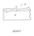
- FIG. 1is a cross-sectional view of a semiconductor wafer fragment depicting an embodiment in accordance with the present invention at an early step in the formation of a dielectric layer.
- FIG. 2is a cross-sectional view of a semiconductor wafer fragment depicting the embodiment of FIG. 1 at a subsequent step in the formation of a dielectric layer.
- FIG. 3is a cross-sectional view of a simplified representation of an MOS transistor formed in accordance with embodiments of the present invention.
- FIG. 4is a cross-sectional view of a simplified representation of a capacitor structure formed in accordance with embodiments of the present invention.
- semiconductor substrateis defined to mean any construction encompassing silicon semiconductive material, including, but not limited to, bulk silicon semiconductive materials such as a silicon semiconductor wafer (either alone or in assemblies encompassing other materials thereon) and silicon semiconductive material layers (either alone or in assemblies encompassing other materials).
- substraterefers to any supporting structure, including, but not limited to, the semiconductor substrates described above.
- high dielectric constant materialor “hi-K material” are used interchangeably herein and refer to materials having a dielectric constant that is greater than that of thermally grown silicon dioxide, which is generally understood to have a value of approximately 3.9 or higher.
- semiconductor wafer fragment 10 ais shown depicted at an early processing step of an embodiment in accordance with the present invention.
- Wafer fragment 10 aencompasses a semiconductive substrate 20 , shown having a surface 22 , a silicon dioxide layer 30 overlying surface 22 , a first metal-containing layer 40 overlying layer 30 and a second metal-containing layer 50 overlying layer 40 .
- semiconductive substrate 20is defined to mean any construction encompassing silicon semiconductive material.
- a cross-sectional representation of such a semiconductive substrate 20will include a variety of doped regions as are needed to form semiconductor device structures. Some of such doped regions, for example well regions, being present even at an early stage of processing. However, for ease of understanding the present invention, such doped regions that may be present are not shown in FIG. 1.
- Surface 22is an outermost boundary of substrate 20 .
- surface 22can be an upper surface of a single crystal silicon substrate, an epitaxially grown silicon layer or any other appropriate silicon-containing material.
- Silicon dioxide layer 30is an optional layer. That is to say that, in some embodiments of the present invention such a layer is present at this early stage in the processing and in some it is not present. In addition, it will be understood that in those embodiments where the optional silicon dioxide layer 30 is present, such layer is either a “native” oxide layer or an oxide layer that is formed to have a specific thickness by a process selected for the forming of such a layer.
- silicon dioxide layer 30is a “native” oxide layer
- silicon dioxide layer 30is a “native” oxide layer
- silicon dioxide layer 30is a purposely grown layer
- such layerresults from exposure of surface 22 to oxidizing conditions such as an oxidizing ambient, at an elevated temperature.
- “native” oxide layersare essentially self-limiting in thickness and are generally limited to about one or two molecular mono-layers in thickness.
- layer 30is a purposely grown layer
- such layercan be formed having essentially any thickness and where employed in embodiments of the present invention, is typically grown to a few nanometers in thickness, for example, 5 nanometers or less, although any other thickness is also appropriate.
- a plasma N 2 O processmay be used to remove substrate native oxide.”
- a plasma N 2 O processmay be used to remove substrate native oxide.”
- embodiments in accordance with the present inventioncan advantageously eliminate such a processing step. That is to say, that in some embodiments of the present invention, where a silicon oxide layer 30 is formed or allowed to form, no specific removal step is needed.
- first metal-containing layer 40is shown overlying optional silicon oxide layer 30 .
- Layer 40is generally formed of a metal selected from the elements of Group IVB of the Periodic Table of the Elements. As known, such group is generally understood to include the elements titanium (Ti), zirconium (Zr), hafnium (Hf) and rutherfordium (Rf) which generally form chemically and thermally stable oxides having attractively high dielectric constants, for example the oxide of hafnium is reported to have a dielectric constant (k) of about 27.
- hafnium-containing layer 40is advantageous since (1) hafnium oxide (HfO 2 ) is the most stable oxide of the group of oxides, (2) hafnium is capable of reducing a silicon oxide layer, (3) hafnium suicide is readily oxidized and (4) HfO 2 is resistive to impurity diffusion.
- hafnium oxideHfO 2
- the thickness of layer 40will be 1 nanometer (nm) or less, while in other embodiments the thickness will be as much as approximately 5 nm or more.
- Such variations in thicknessare a function of, among other things, the use or non-use of the optional silicon dioxide layer 30 , and the purpose for which a finally formed dielectric layer, in accordance with the present invention, is intended.
- a gate dielectric layeris formed and in other embodiments of the present invention a capacitor dielectric layer is formed.
- the thickness of such layerscan vary widely.
- Metal-containing layer 40is most advantageously formed by a physical vapor deposition process (PVD). While any of the several common PVD processes such as sputtering or evaporation can be used, it is found advantageous to use an evaporative processes and in particular an electron beam evaporative process. For example, where an electron beam evaporative process is employed, it is found that an initial purity level of the source material for the PVD process can be provided to layer 40 . That is to say that the level of purity of the source material and initially deposited metal-containing layer is essentially unchanged.
- PVDphysical vapor deposition process
- metal-containing layer 40is within the scope and spirit of the present invention, for example evaporation methods where a heating source other than an electron beam is employed or any other appropriate PVD method capable of providing the initial purity level of the source material to layer 40 , can also be advantageously used.
- metal-containing layer 50is shown overlying first metal layer 40 .
- metal-containing layer 50is advantageously formed of a metal selected from the elements of Group IIIB of the Periodic Table of the Elements.
- Group IIIBis generally understood to encompass scandium (Sc), yttrium (Y), lanthanum (La) and actinium (Ac).
- Embodiments of the present inventionencompass Group IIIB elements, as such elements form dielectric oxides that have high thermodynamic stability and a generally suitable dielectric constant.
- lanthanum oxideLa 2 O 3
- La 2 O 3has high thermodynamic stability.
- metal-containing layer 50is formed in the same manner as is metal-containing layer 40 . That is to say, by using a physical deposition (PVD) method as previously described.
- PVDphysical deposition
- layers 40 and 50can be formed in distinct PVD processes, it is generally advantageous to form both layers using a single, unified PVD process.
- a unified deposition or forming processwould generally provide that substrate 10 a is placed into a PVD system and a material of the first metal-containing layer 40 is formed thereon until a desired thickness of layer 40 is formed.
- the forming of first layer 40is stopped and a forming of second layer 50 is begun within the same PVD system.
- the forming of second layer 50is stopped once a desired second thickness for such layer is obtained or when a desired total thickness of layers 40 and 50 is obtained.
- the forming of layer 50is begun without a prior stopping of the deposition of the material of layer 40 .
- the material of second metal-containing layer 50will be combined with some material of first metal-containing layer 40 in at least an interfacial region (not shown) of such second layer 50 .
- an interfacial regionnot shown
- such a mixing of the materials of first layer 40 and second layer 50is limited to such an interfacial region by stopping the forming of the material of layer 40 after the forming of the material of layer 50 is started.
- the forming of the material of layer 40is not stopped once the forming of the material of layer 50 is started, rather both materials are formed until a desired thickness is obtained thus, essentially all of second layer 50 is a mixture of materials.
- a desired thickness for second metal-containing layer 50can also vary as a function of the several factors mentioned for layer 40 as well as the thickness of first layer 40 previously deposited. Thus, the thickness of such layer 50 generally has the same range as provided above for the thickness of layer 40 .
- first layer 40 to second layer 50a specific ratio of thickness for first layer 40 to second layer 50 is advantageous.
- a thin layer of a hafnium-containing metal layer 40is formed, about 1 nm or less, and employed to reduce such silicon oxide layer 30 prior to forming second layer 50 .
- the subsequent second metal-containing layer 50is formed with an appropriate thickness, for example a layer of lanthanum-containing metal having a thickness of between about 3 to 5 nm.
- Advantageous thickness ratios of first metal-containing layer 40 to second metal-containing layer 50have been found to vary with ratios from about 1:5 to about 5:1 being typical.
- FIG. 2a cross-sectional view of a semiconductor wafer fragment 10 b depicting the embodiment of FIG. 1 at a subsequent processing step is depicted. As shown, a first metal-containing dielectric layer 45 overlies surface 22 of semiconductive substrate 20 and a second metal-containing dielectric layer 55 overlies the first layer 45 .
- First metal-containing dielectric layer 45 and second metal-containing dielectric layer 55are formed from first metal-containing layer 40 and second metal-containing layer 50 (of FIG. 1), respectively.
- a transformation from metal-containing layers to metal-containing dielectric layersis performed.
- Such transformationtypically encompassing oxidizing the metal-containing layers to form amorphous metal oxide containing material layers.
- such an oxidation processis accomplished after deposition of both the first and second metal-containing layers.
- oxidation of the first metal-containing layer to form the first metal-containing dielectric layerprecedes formation of the second metal-containing layer.
- oxidation of one or both of the metal-containing layersis performed, during the forming of one or the other of such layers.
- a hafnium-containing layer 40is formed over layer 30 and subsequently exposed to conditions such that the hafnium of layer 40 combines with the oxygen of silicon oxide layer 30 to form a hafnium-containing dielectric layer 45 comprising hafnium oxide (HfO 2 ).
- hafnium-containing dielectric layer 45comprising hafnium oxide (HfO 2 ).
- silicon dioxide layer 30is reduced to silicon, the thickness of such layer 30 is combined with substrate 20 in FIG. 2.
- hafnium metal-containing layeris oxidized, a second lanthanum-containing layer is formed and subsequently oxidized by an appropriate method. While such example specifically refers to Hf and La, it will be understood that the other elements of Group IVB and IIIB, such as Zr and Y, respectively, could also be employed, although the relative reactivity of the materials will vary.
- conditions for the chemical reduction of optional silicon oxide layer 30 with the material of layer 40encompass providing temperatures between about 200° C. and 400° C. as an inert atmosphere is typically provided such that layer 30 is essentially the only source of oxygen present.
- silicon oxide layer 30is not present, or after the chemical reduction of such silicon dioxide layer, other methods for the oxidation of portions of layer 40 not completely oxidized and/or layer 50 are employed. Such other methods include, but are not limited to, the use of remotely formed oxygen radicals; ion bombardment of such metal layers with oxygen ions and thermal oxidation of such layers in an oxygen comprising atmosphere at appropriate temperatures.
- Such low energy ion bombardmentis performed using relatively high plasma densities, typically above 10 12 /cm 3 , and low electron temperature, generally less than 1.3 eV, and where oxygen radicals are used, generally such radicals are formed using appropriate radio frequency or microwave energy which is applied to an oxygen comprising gas stream at a reduced pressure.
- oxygen radicalsgenerally such radicals are formed using appropriate radio frequency or microwave energy which is applied to an oxygen comprising gas stream at a reduced pressure.
- oxygen radicalsgenerally the use of ion bombardment and/or oxygen radicals is provided in combination with a thermal treatment.
- the layersare held in such gas mixture at a pressure of about 1 Torr and a temperature of about 250° C. to about 300° C. with a microwave power source applying a power density of about 3-7 W/cm 2 . It will be understood that such oxidation conditions only one effective method and that other appropriate and effective methods can be used to form one or both of dielectric layers 45 and 55 from layers 40 and 50 either collectively or individually.
- gate dielectric 60is disposed over a portion of surface 22 of substrate 20 as well as adjacent to and elevationally above source/drain (S/D) regions 24 .
- gate dielectric 60encompasses metal-containing dielectric layers 45 and 55 (FIG. 2) where such layers are formed as described above and subsequently patterned using any of the appropriate methods for patterning a gate electrode and dielectric.
- S/D regions 24 and sidewall spacers 70are also formed by appropriate methods. It will be understood that transistor 14 is a simplified transistor representation, and that more complex transistor structures are also encompassed by embodiments of the present invention.
- transistor 14is a MOSFET having an gate dielectric layer 60 that has an equivalent oxide thickness (EOT) of 2 nm or less while having an actual thickness of as much as about 6 nm.
- EOTequivalent oxide thickness
- Such an advanced MOSFETcan also have a gate length of about 0.25 micron or less and be encompassed within an integrated circuit such as a dynamic random access memory (DRAM), static random access memory (SRAM) or any of the various other memory integrated circuits.
- Transistor 14can also encompass a gate dielectric layer 60 that has an EOT of greater than 2 nm and a gate length of more than 0.25 micron.
- Transistor or integrated circuit embodiments in accordance with the present inventionthat have an equivalent oxide thickness of about 2 nm or less, advantageously provide for readily forming gate dielectric layer 60 having a desired EOT that would not be otherwise practical.
- methods for incorporating materials with high-dielectric constants, such as oxides of Group IIIB and IVB metals, over a silicon substrateare provided where such materials can be formed into a stacked amorphous metal oxide-containing gate dielectric structure such as gate dielectric 60 .
- FIG. 4a simplified capacitor structure 16 , formed in accordance with embodiments of the present invention, is depicted.
- Capacitor structure 16is shown overlying a doped region 26 , disposed in semiconductive substrate 20 .
- a lower capacitor electrode 82electrically contacts region 26
- a capacitor dielectric 64overlies electrode 82 and a second capacitor electrode 86 overlies capacitor dielectric 64 .
- Capacitor dielectric 64is advantageously formed from first and second metal-containing layers deposited over lower electrode 82 in a manner analogous to that described previously with FIGS. 1 and 2. Thus, after first forming and patterning lower capacitor electrode 82 , first and second metal-containing layers (not shown) are formed and transformed by appropriate methods into metal-containing dielectric layers which are encompassed within capacitor dielectric layer 64 .
- Group IVB and IIIB metals into metal oxidesare not limited to extremely thin films, thus thicker metal-containing layers, suitable for forming capacitor dielectric layers having a thickness of 10 nm or more, can be first deposited and then transformed into a metal-containing dielectric layer.
- Group IVB metal oxides in general and HfO 2 in particularare/is resistant to impurity diffusion so that such materials can be oxidized over a lower capacitor electrode 82 formed from silicon-comprising materials such as any of the various forms of polycrystalline silicon without oxidizing such lower electrode 82 .
Landscapes
- Engineering & Computer Science (AREA)
- Microelectronics & Electronic Packaging (AREA)
- Condensed Matter Physics & Semiconductors (AREA)
- General Physics & Mathematics (AREA)
- Manufacturing & Machinery (AREA)
- Computer Hardware Design (AREA)
- Physics & Mathematics (AREA)
- Power Engineering (AREA)
- Chemical & Material Sciences (AREA)
- Chemical Kinetics & Catalysis (AREA)
- Crystallography & Structural Chemistry (AREA)
- General Chemical & Material Sciences (AREA)
- Insulated Gate Type Field-Effect Transistor (AREA)
- Formation Of Insulating Films (AREA)
- Semiconductor Integrated Circuits (AREA)
Abstract
Description
- The present invention relates generally to methods of forming dielectric layers and the devices fabricated therewith. More specifically, the present invention relates to methods of forming dielectric layers having high dielectric constants by depositing oxidizable materials over a semiconductor substrate and oxidizing the materials to form amorphous oxides. The invention also pertains to devices formed employing such oxides.[0001]
- Increasing the performance of integrated circuits (ICs), both with regard to more complex functionality and higher speeds, is a primary goal of efforts in advancing the semiconductor arts. One method that has been extensively employed to achieve this goal is scaling, that is decreasing area or size of individual device components that are used to form such integrated circuits. For example, the gate length of a typical MOS transistor has been reduced over the past several years from several microns to fractions of a micron and gate lengths of 0.1 micron or less will soon be desired. Such scaling efforts have also effected the size of capacitors used in a variety of ICs such as DRAMS and SRAMS (dynamic and static random access memories, respectively).[0002]
- While such scaling efforts have resulted in the desired increases in performance, generally such size reductions also impact at least some characteristics of the devices so “scaled.” For example, reducing the gate length of a transistor generally reduces the transistor's output and decreasing the size of a capacitor generally reduces the capacitance or amount of charge such a capacitor can store. Fortunately, changing other features of devices such as transistors and capacitors has made it possible to retain or at least control such changes in their aforementioned characteristics. Thus as transistor gate length has been reduced, the gate dielectric layer's thickness has also been reduced to at least partially compensate for the change in device output. Similarly, as the size of capacitor structures has been reduced, materials such as hemispherically grained polysilicon (HSG) have been employed to increase the effective surface area of such structures and compensate, at least in part, for such size reductions.[0003]
- However, it appears likely that as scaling continues such exemplary compensation techniques may not be possible. Silicon dioxide (SiO[0004]2), with a dielectric constant of about 3.9, remains the most common material employed for gate dielectric layers. To maintain transistor output at an acceptable level, a transistor having a gate length of 0.1 micron will require an ultra-thin SiO2layer with a thickness of about 2 nanometers (nm). Ultra-thin being defined herein as a thickness of about 5 nm or less.
- The forming and use of such ultra-thin SiO[0005]2layers is problematic for a variety of reasons since such layers consist of only a few layers of molecules. Thus only one additional or missing layer of molecules can have a dramatic effect on device performance; for example where a desired layer is four SiO2molecules thick, a change of one molecule will change a characteristic such as the layer's capacitance by as much as 25%. In addition, such thin layers typically exhibit high current leakage, for example due to band to band or Fowler-Nordheim tunneling. Such layers are also more susceptible to dopant penetration or diffusion through the layer thus changing the characteristics of an adjacent layer or region; for example boron diffusion from the gate electrode into the channel region alters channel characteristics.
- One method of reducing these problems is the use of a thicker layer of an alternative dielectric material such as a metal oxide having a higher dielectric constant than that of SiO[0006]2. For the purpose of illustration, a metal oxide gate dielectric having an appropriately high dielectric constant can be formed with a thickness several times that of a SiO2layer while having the performance characteristics of the thinner SiO2layer. Thus the thicker metal oxide layer is said to have the equivalent oxide thickness (EOT) of the thinner layer. Alternate metal oxide materials such as titanium oxide (TiO2), aluminum oxide (Al2O3), tantalum oxide (Ta2O5) and others have therefore received attention as replacements for SiO2. However, such alternate materials must exhibit, in addition to a high dielectric constant (greater than that of SiO2), a large band-gap with a favorable band alignment, low interface state density, good thermal stability and the ability to be formed in a manner consistent with known semiconductor process methods at reasonable cost and yield. Unfortunately, many candidate metal oxide materials having an appropriately high dielectric constant, cannot meet these additional requirements. Thus it would desirable provide alternate dielectric materials and methods of forming such materials that are appropriate as a replacement for ultra-thin SiO2layers.
- Embodiments in accordance with the present invention provide dielectric materials, methods of forming such dielectric materials, and semiconductor devices that employ such dielectric materials. Such embodiments provide for the forming of a first metal-containing dielectric layer over a silicon-containing surface of a substrate and the forming of a second metal-containing dielectric layer on the first layer. In embodiments of the present invention, the first and second metal-containing dielectric layers encompass elements selected from Group IVB and Group IIIB of the Periodic Table of Elements, respectively.[0007]
- In some embodiments, a silicon dioxide layer is first formed and a first metal-containing layer is formed overlying such silicon dioxide layer. Advantageously, the metal of the first layer encompasses an element that can combine with the oxygen of the silicon dioxide to form a metal oxide material of the first metal-containing dielectric layer and chemically reduce the silicon dioxide to silicon.[0008]
- In some embodiments in accordance with the present invention, one or more metal-containing layers are exposed to an atmosphere that encompasses oxygen while heating the exposed layers to a temperature effective to transform such metal-containing layers to metal-containing dielectric oxide layers. In some embodiments, such exposing encompasses ion bombardment of the metal-containing layers, and in some embodiments such exposing encompasses providing oxygen radicals to the metal-containing layers.[0009]
- Embodiments in accordance with the present invention provide for forming the first and second metal-containing dielectric layers having a wide ratio of relative thicknesses, for example from a ratio of about 1:5 to about 5:1 or greater. In embodiments of the present invention, such forming can be provided by physical vapor deposition (PVD) where a metal-containing layer of each formed layer is first deposited having a thickness of about 10 nanometers (nm) or less. In embodiments of the present invention, such PVD methods include electron beam evaporation techniques or other methods for forming high purity material layers by PVD. For example in some embodiments, radio frequency or microwave energy is employed for heating rather than an electron beam.[0010]
- Embodiments of the present invention can encompass semiconductor devices such as MOS transistors, capacitors and the like. Such devices are formed using metal-containing dielectric layers in accordance with the present invention.[0011]
- Some embodiments encompass integrated circuits such as dynamic and static random access memories (DRAMs and SRAMs) which include transistors, capacitors and the like that are formed employing metal-containing dielectric layers in accordance with the present invention, where such layers are also formed by methods in accordance with the present invention. In some embodiments of the present invention, semiconductor devices encompassing a metal-containing containing dielectric layer have an equivalent oxide thickness (EOT) of 2 nm to 5 nm. Advantageously, metal-containing dielectric layers in accordance with the present invention having an EOT of less than 2 nm are also possible.[0012]
- Embodiments in accordance with the present invention are described below with reference to the following accompanying drawings.[0013]
- FIG. 1 is a cross-sectional view of a semiconductor wafer fragment depicting an embodiment in accordance with the present invention at an early step in the formation of a dielectric layer.[0014]
- FIG. 2 is a cross-sectional view of a semiconductor wafer fragment depicting the embodiment of FIG. 1 at a subsequent step in the formation of a dielectric layer.[0015]
- FIG. 3 is a cross-sectional view of a simplified representation of an MOS transistor formed in accordance with embodiments of the present invention.[0016]
- FIG. 4 is a cross-sectional view of a simplified representation of a capacitor structure formed in accordance with embodiments of the present invention.[0017]
- This disclosure of the invention is submitted in furtherance of the constitutional purposes of the U.S. Patent Laws “to promote the progress of science and useful arts” (Article 1, Section 8).[0018]
- Embodiments in accordance with the present invention will be described with reference to the aforementioned figures. Various modifications, adaptations or variations of the specific methods and or structures described may become apparent to those skilled in the art as embodiments of the present invention are described. All such modifications, adaptations or variations, that rely upon the teachings of the present invention, and through which these teachings have advanced the art, are considered to be within the scope and spirit of the present invention.[0019]
- To aid in interpretation of the description of the illustrations and claims that follow, the term “semiconductor substrate” is defined to mean any construction encompassing silicon semiconductive material, including, but not limited to, bulk silicon semiconductive materials such as a silicon semiconductor wafer (either alone or in assemblies encompassing other materials thereon) and silicon semiconductive material layers (either alone or in assemblies encompassing other materials). The term “substrate” refers to any supporting structure, including, but not limited to, the semiconductor substrates described above. In addition, the terms “high dielectric constant material” or “hi-K material” are used interchangeably herein and refer to materials having a dielectric constant that is greater than that of thermally grown silicon dioxide, which is generally understood to have a value of approximately 3.9 or higher.[0020]
- Referring to FIG. 1,[0021]
semiconductor wafer fragment 10ais shown depicted at an early processing step of an embodiment in accordance with the present invention. Waferfragment 10aencompasses asemiconductive substrate 20, shown having asurface 22, asilicon dioxide layer 30 overlyingsurface 22, a first metal-containinglayer 40 overlyinglayer 30 and a second metal-containinglayer 50 overlyinglayer 40. - As described above,[0022]
semiconductive substrate 20 is defined to mean any construction encompassing silicon semiconductive material. Generally a cross-sectional representation of such asemiconductive substrate 20, will include a variety of doped regions as are needed to form semiconductor device structures. Some of such doped regions, for example well regions, being present even at an early stage of processing. However, for ease of understanding the present invention, such doped regions that may be present are not shown in FIG. 1. - [0023]
Surface 22 is an outermost boundary ofsubstrate 20. For illustrative purposes,surface 22 can be an upper surface of a single crystal silicon substrate, an epitaxially grown silicon layer or any other appropriate silicon-containing material.Silicon dioxide layer 30 is an optional layer. That is to say that, in some embodiments of the present invention such a layer is present at this early stage in the processing and in some it is not present. In addition, it will be understood that in those embodiments where the optionalsilicon dioxide layer 30 is present, such layer is either a “native” oxide layer or an oxide layer that is formed to have a specific thickness by a process selected for the forming of such a layer. Wheresilicon dioxide layer 30 is a “native” oxide layer, it will be understood that such a layer is formed spontaneously upon exposure ofsilicon surface 22 to an oxygen-containing ambient, generally at or near room temperature. Alternatively, wheresilicon dioxide layer 30 is a purposely grown layer, such layer results from exposure ofsurface 22 to oxidizing conditions such as an oxidizing ambient, at an elevated temperature. Furthermore it will be understood that “native” oxide layers are essentially self-limiting in thickness and are generally limited to about one or two molecular mono-layers in thickness. However, wherelayer 30 is a purposely grown layer, such layer can be formed having essentially any thickness and where employed in embodiments of the present invention, is typically grown to a few nanometers in thickness, for example, 5 nanometers or less, although any other thickness is also appropriate. - Generally, where electrical contact to surface[0024]22 is desired, it is known to remove such a layer as
oxide layer 30 from over all or some portions ofsurface 22 prior to forming any layer from which the electrical contact will be made. For example, Maiti et al. (U.S. Pat. No. 6,020,024, entitled “Method for Forming High Dielectric Constant Metal Oxides,” hereinafter US'024) state at column 2, lines 61-65, that semiconductor substrate12 (FIG. 1) “has preferably been pre-cleaned in order to minimize the oxide at its surface with an HF clean and/or hydrogen (H2) anneal step. In an alternative, a plasma N2O process may be used to remove substrate native oxide.” As will be described below, embodiments in accordance with the present invention can advantageously eliminate such a processing step. That is to say, that in some embodiments of the present invention, where asilicon oxide layer 30 is formed or allowed to form, no specific removal step is needed. - Still referring to FIG. 1, first metal-containing[0025]
layer 40 is shown overlying optionalsilicon oxide layer 30.Layer 40 is generally formed of a metal selected from the elements of Group IVB of the Periodic Table of the Elements. As known, such group is generally understood to include the elements titanium (Ti), zirconium (Zr), hafnium (Hf) and rutherfordium (Rf) which generally form chemically and thermally stable oxides having attractively high dielectric constants, for example the oxide of hafnium is reported to have a dielectric constant (k) of about 27. While embodiments of the present invention encompass any of the Group IVB elements, it has been found that a hafnium-containinglayer 40 is advantageous since (1) hafnium oxide (HfO2) is the most stable oxide of the group of oxides, (2) hafnium is capable of reducing a silicon oxide layer, (3) hafnium suicide is readily oxidized and (4) HfO2is resistive to impurity diffusion. - In some embodiments of the present invention, the thickness of[0026]
layer 40 will be 1 nanometer (nm) or less, while in other embodiments the thickness will be as much as approximately 5 nm or more. Such variations in thickness are a function of, among other things, the use or non-use of the optionalsilicon dioxide layer 30, and the purpose for which a finally formed dielectric layer, in accordance with the present invention, is intended. For example, as will be discussed below, in some embodiments of the present invention a gate dielectric layer is formed and in other embodiments of the present invention a capacitor dielectric layer is formed. As one of ordinary skill in the art is aware, the thickness of such layers can vary widely. - Metal-containing[0027]
layer 40 is most advantageously formed by a physical vapor deposition process (PVD). While any of the several common PVD processes such as sputtering or evaporation can be used, it is found advantageous to use an evaporative processes and in particular an electron beam evaporative process. For example, where an electron beam evaporative process is employed, it is found that an initial purity level of the source material for the PVD process can be provided tolayer 40. That is to say that the level of purity of the source material and initially deposited metal-containing layer is essentially unchanged. However, it will be understood that the other methods of forming metal-containinglayer 40 are within the scope and spirit of the present invention, for example evaporation methods where a heating source other than an electron beam is employed or any other appropriate PVD method capable of providing the initial purity level of the source material to layer40, can also be advantageously used. - Still referring to FIG. 1, second metal-containing[0028]
layer 50 is shown overlyingfirst metal layer 40. In accordance with embodiments of the present invention, metal-containinglayer 50 is advantageously formed of a metal selected from the elements of Group IIIB of the Periodic Table of the Elements. As known, Group IIIB is generally understood to encompass scandium (Sc), yttrium (Y), lanthanum (La) and actinium (Ac). Embodiments of the present invention encompass Group IIIB elements, as such elements form dielectric oxides that have high thermodynamic stability and a generally suitable dielectric constant. Of such Group IIIB elements, it has been found that a lanthanum-containinglayer 50 is advantageous at least because (1) lanthanum oxide (La2O3) has a dielectric constant similar to that of HfO2(k=27 for La2O3and k=24 for HfO2) and (2) La2O3has high thermodynamic stability. Thus changes in the relative thickness forlayers - Generally, metal-containing[0029]
layer 50 is formed in the same manner as is metal-containinglayer 40. That is to say, by using a physical deposition (PVD) method as previously described. However, whilelayers substrate 10ais placed into a PVD system and a material of the first metal-containinglayer 40 is formed thereon until a desired thickness oflayer 40 is formed. In some embodiments, once a first thickness offirst layer 40 is obtained, the forming offirst layer 40 is stopped and a forming ofsecond layer 50 is begun within the same PVD system. Subsequently, the forming ofsecond layer 50 is stopped once a desired second thickness for such layer is obtained or when a desired total thickness oflayers - In some embodiments, after the first thickness of[0030]
layer 40 is formed, the forming oflayer 50 is begun without a prior stopping of the deposition of the material oflayer 40. In this manner the material of second metal-containinglayer 50 will be combined with some material of first metal-containinglayer 40 in at least an interfacial region (not shown) of suchsecond layer 50. It will be understood that in some embodiments, such a mixing of the materials offirst layer 40 andsecond layer 50 is limited to such an interfacial region by stopping the forming of the material oflayer 40 after the forming of the material oflayer 50 is started. In other embodiments, the forming of the material oflayer 40 is not stopped once the forming of the material oflayer 50 is started, rather both materials are formed until a desired thickness is obtained thus, essentially all ofsecond layer 50 is a mixture of materials. In addition, as discussed for first metal-containinglayer 40, a desired thickness for second metal-containinglayer 50 can also vary as a function of the several factors mentioned forlayer 40 as well as the thickness offirst layer 40 previously deposited. Thus, the thickness ofsuch layer 50 generally has the same range as provided above for the thickness oflayer 40. - It has also been found that in some embodiments in accordance with the present invention a specific ratio of thickness for[0031]
first layer 40 tosecond layer 50 is advantageous. For example where an optionalsilicon oxide layer 30 is used, generally a thin layer of a hafnium-containingmetal layer 40 is formed, about 1 nm or less, and employed to reduce suchsilicon oxide layer 30 prior to formingsecond layer 50. The subsequent second metal-containinglayer 50 is formed with an appropriate thickness, for example a layer of lanthanum-containing metal having a thickness of between about 3 to 5 nm. Advantageous thickness ratios of first metal-containinglayer 40 to second metal-containinglayer 50 have been found to vary with ratios from about 1:5 to about 5:1 being typical. - Turning now to FIG. 2, a cross-sectional view of a[0032]
semiconductor wafer fragment 10bdepicting the embodiment of FIG. 1 at a subsequent processing step is depicted. As shown, a first metal-containingdielectric layer 45 overlies surface22 ofsemiconductive substrate 20 and a second metal-containingdielectric layer 55 overlies thefirst layer 45. - First metal-containing[0033]
dielectric layer 45 and second metal-containingdielectric layer 55 are formed from first metal-containinglayer 40 and second metal-containing layer50 (of FIG. 1), respectively. Generally, a transformation from metal-containing layers to metal-containing dielectric layers is performed. Such transformation typically encompassing oxidizing the metal-containing layers to form amorphous metal oxide containing material layers. In some embodiments of the present invention, such an oxidation process is accomplished after deposition of both the first and second metal-containing layers. In other embodiments oxidation of the first metal-containing layer to form the first metal-containing dielectric layer precedes formation of the second metal-containing layer. In yet other embodiments of the present invention, oxidation of one or both of the metal-containing layers is performed, during the forming of one or the other of such layers. By means of example, in one such method where optionalsilicon oxide layer 30 is present, a hafnium-containinglayer 40 is formed overlayer 30 and subsequently exposed to conditions such that the hafnium oflayer 40 combines with the oxygen ofsilicon oxide layer 30 to form a hafnium-containingdielectric layer 45 comprising hafnium oxide (HfO2). Such a method of forming a metal oxide by the chemical reduction of silicon dioxide oflayer 30 to silicon makes it possible to skip the separate removal step for the silicon oxide layer that is taught by Maiti et al. in the previously mentioned US'024. It will be noted that sincesilicon dioxide layer 30 is reduced to silicon, the thickness ofsuch layer 30 is combined withsubstrate 20 in FIG. 2. When such hafnium metal-containing layer is oxidized, a second lanthanum-containing layer is formed and subsequently oxidized by an appropriate method. While such example specifically refers to Hf and La, it will be understood that the other elements of Group IVB and IIIB, such as Zr and Y, respectively, could also be employed, although the relative reactivity of the materials will vary. - Generally, conditions for the chemical reduction of optional[0034]
silicon oxide layer 30 with the material oflayer 40 encompass providing temperatures between about 200° C. and 400° C. as an inert atmosphere is typically provided such thatlayer 30 is essentially the only source of oxygen present. However, wheresilicon oxide layer 30 is not present, or after the chemical reduction of such silicon dioxide layer, other methods for the oxidation of portions oflayer 40 not completely oxidized and/orlayer 50 are employed. Such other methods include, but are not limited to, the use of remotely formed oxygen radicals; ion bombardment of such metal layers with oxygen ions and thermal oxidation of such layers in an oxygen comprising atmosphere at appropriate temperatures. Typically such low energy ion bombardment is performed using relatively high plasma densities, typically above 1012/cm3, and low electron temperature, generally less than 1.3 eV, and where oxygen radicals are used, generally such radicals are formed using appropriate radio frequency or microwave energy which is applied to an oxygen comprising gas stream at a reduced pressure. In addition, generally the use of ion bombardment and/or oxygen radicals is provided in combination with a thermal treatment. By means of example, it is found effective to convert metal-containinglayers dielectric layers dielectric layers layers - Referring to FIG. 3, an[0035]
MOS transistor 14 formed in accordance with embodiments of the present invention is depicted.Gate dielectric 60 is disposed over a portion ofsurface 22 ofsubstrate 20 as well as adjacent to and elevationally above source/drain (S/D)regions 24. In accordance with embodiments of the present invention,gate dielectric 60 encompasses metal-containingdielectric layers 45 and55 (FIG. 2) where such layers are formed as described above and subsequently patterned using any of the appropriate methods for patterning a gate electrode and dielectric. S/D regions 24 andsidewall spacers 70 are also formed by appropriate methods. It will be understood thattransistor 14 is a simplified transistor representation, and that more complex transistor structures are also encompassed by embodiments of the present invention. For example, in some embodiments,transistor 14 is a MOSFET having angate dielectric layer 60 that has an equivalent oxide thickness (EOT) of 2 nm or less while having an actual thickness of as much as about 6 nm. Such an advanced MOSFET can also have a gate length of about 0.25 micron or less and be encompassed within an integrated circuit such as a dynamic random access memory (DRAM), static random access memory (SRAM) or any of the various other memory integrated circuits.Transistor 14 can also encompass agate dielectric layer 60 that has an EOT of greater than 2 nm and a gate length of more than 0.25 micron. - Transistor or integrated circuit embodiments in accordance with the present invention that have an equivalent oxide thickness of about 2 nm or less, advantageously provide for readily forming[0036]
gate dielectric layer 60 having a desired EOT that would not be otherwise practical. Thus, methods for incorporating materials with high-dielectric constants, such as oxides of Group IIIB and IVB metals, over a silicon substrate are provided where such materials can be formed into a stacked amorphous metal oxide-containing gate dielectric structure such asgate dielectric 60. - Turning now to FIG. 4 a[0037]
simplified capacitor structure 16, formed in accordance with embodiments of the present invention, is depicted.Capacitor structure 16 is shown overlying a dopedregion 26, disposed insemiconductive substrate 20. Alower capacitor electrode 82electrically contacts region 26, acapacitor dielectric 64 overlieselectrode 82 and asecond capacitor electrode 86 overliescapacitor dielectric 64. - [0038]
Capacitor dielectric 64 is advantageously formed from first and second metal-containing layers deposited overlower electrode 82 in a manner analogous to that described previously with FIGS. 1 and 2. Thus, after first forming and patterninglower capacitor electrode 82, first and second metal-containing layers (not shown) are formed and transformed by appropriate methods into metal-containing dielectric layers which are encompassed withincapacitor dielectric layer 64. - The previously described methods of converting Group IVB and IIIB metals into metal oxides are not limited to extremely thin films, thus thicker metal-containing layers, suitable for forming capacitor dielectric layers having a thickness of 10 nm or more, can be first deposited and then transformed into a metal-containing dielectric layer. As previously mentioned, Group IVB metal oxides in general and HfO[0039]2in particular, are/is resistant to impurity diffusion so that such materials can be oxidized over a
lower capacitor electrode 82 formed from silicon-comprising materials such as any of the various forms of polycrystalline silicon without oxidizing suchlower electrode 82. - In compliance with the statute, the invention has been described in language more or less specific as to structural and methodical features. In addition, advantages of the invention of the instant application have become apparent by and through the descriptions and examples provided. Thus it will be understood that the use of stacked amorphous gate oxide layers formed of Group IVB and IIIB metal oxides advantageously provides a final layer that has a high dielectric constant of about 27 to 29, and is both thermally stable and protective of underlying layers to impurity diffusion. It will be understood that the selection of Hf and La form the metal-containing layers is particularly advantageous although other metals from Group IVB and IIIB are also appropriate. It is to be understood, however, that the invention is not limited to the specific features shown and described, since the means herein disclosed comprise preferred forms of putting the invention into effect. The invention is, therefore, claimed in any of its forms or modifications within the proper scope of the appended claims appropriately interpreted in accordance with the doctrine of equivalents.[0040]
Claims (51)
Priority Applications (2)
| Application Number | Priority Date | Filing Date | Title |
|---|---|---|---|
| US10/174,434US7420239B2 (en) | 2001-06-13 | 2002-06-17 | Dielectric layer forming method and devices formed therewith |
| US10/931,544US7465982B2 (en) | 2001-06-13 | 2004-08-31 | Capacitor structures |
Applications Claiming Priority (2)
| Application Number | Priority Date | Filing Date | Title |
|---|---|---|---|
| US09/881,408US7037862B2 (en) | 2001-06-13 | 2001-06-13 | Dielectric layer forming method and devices formed therewith |
| US10/174,434US7420239B2 (en) | 2001-06-13 | 2002-06-17 | Dielectric layer forming method and devices formed therewith |
Related Parent Applications (1)
| Application Number | Title | Priority Date | Filing Date |
|---|---|---|---|
| US09/881,408DivisionUS7037862B2 (en) | 2001-06-13 | 2001-06-13 | Dielectric layer forming method and devices formed therewith |
Related Child Applications (1)
| Application Number | Title | Priority Date | Filing Date |
|---|---|---|---|
| US10/931,544DivisionUS7465982B2 (en) | 2001-06-13 | 2004-08-31 | Capacitor structures |
Publications (2)
| Publication Number | Publication Date |
|---|---|
| US20020192975A1true US20020192975A1 (en) | 2002-12-19 |
| US7420239B2 US7420239B2 (en) | 2008-09-02 |
Family
ID=25378412
Family Applications (5)
| Application Number | Title | Priority Date | Filing Date |
|---|---|---|---|
| US09/881,408Expired - LifetimeUS7037862B2 (en) | 2001-06-13 | 2001-06-13 | Dielectric layer forming method and devices formed therewith |
| US10/174,436Expired - LifetimeUS6787413B2 (en) | 2001-06-13 | 2002-06-17 | Capacitor structure forming methods |
| US10/174,434Expired - LifetimeUS7420239B2 (en) | 2001-06-13 | 2002-06-17 | Dielectric layer forming method and devices formed therewith |
| US10/931,544Expired - LifetimeUS7465982B2 (en) | 2001-06-13 | 2004-08-31 | Capacitor structures |
| US11/133,061Expired - LifetimeUS7235448B2 (en) | 2001-06-13 | 2005-05-19 | Dielectric layer forming method and devices formed therewith |
Family Applications Before (2)
| Application Number | Title | Priority Date | Filing Date |
|---|---|---|---|
| US09/881,408Expired - LifetimeUS7037862B2 (en) | 2001-06-13 | 2001-06-13 | Dielectric layer forming method and devices formed therewith |
| US10/174,436Expired - LifetimeUS6787413B2 (en) | 2001-06-13 | 2002-06-17 | Capacitor structure forming methods |
Family Applications After (2)
| Application Number | Title | Priority Date | Filing Date |
|---|---|---|---|
| US10/931,544Expired - LifetimeUS7465982B2 (en) | 2001-06-13 | 2004-08-31 | Capacitor structures |
| US11/133,061Expired - LifetimeUS7235448B2 (en) | 2001-06-13 | 2005-05-19 | Dielectric layer forming method and devices formed therewith |
Country Status (1)
| Country | Link |
|---|---|
| US (5) | US7037862B2 (en) |
Cited By (47)
| Publication number | Priority date | Publication date | Assignee | Title |
|---|---|---|---|---|
| US20050164445A1 (en)* | 2004-01-23 | 2005-07-28 | Taiwan Semiconductor Manufacturing Co., Ltd. | System and method for integration of HfO2 and RTCVD poly-silicon |
| US6979855B2 (en) | 2001-12-20 | 2005-12-27 | Micron Technology, Inc. | High-quality praseodymium gate dielectrics |
| US7026694B2 (en) | 2002-08-15 | 2006-04-11 | Micron Technology, Inc. | Lanthanide doped TiOx dielectric films by plasma oxidation |
| US7049192B2 (en) | 2003-06-24 | 2006-05-23 | Micron Technology, Inc. | Lanthanide oxide / hafnium oxide dielectrics |
| US7081421B2 (en) | 2004-08-26 | 2006-07-25 | Micron Technology, Inc. | Lanthanide oxide dielectric layer |
| US7084078B2 (en) | 2002-08-29 | 2006-08-01 | Micron Technology, Inc. | Atomic layer deposited lanthanide doped TiOx dielectric films |
| US20060183272A1 (en)* | 2005-02-15 | 2006-08-17 | Micron Technology, Inc. | Atomic layer deposition of Zr3N4/ZrO2 films as gate dielectrics |
| US20060228868A1 (en)* | 2005-03-29 | 2006-10-12 | Micron Technology, Inc. | ALD of amorphous lanthanide doped TiOx films |
| US20060244100A1 (en)* | 2005-04-28 | 2006-11-02 | Micron Technology, Inc. | Atomic layer deposited zirconium silicon oxide films |
| US7135421B2 (en) | 2002-06-05 | 2006-11-14 | Micron Technology, Inc. | Atomic layer-deposited hafnium aluminum oxide |
| US7135369B2 (en) | 2003-03-31 | 2006-11-14 | Micron Technology, Inc. | Atomic layer deposited ZrAlxOy dielectric layers including Zr4AlO9 |
| US7160577B2 (en) | 2002-05-02 | 2007-01-09 | Micron Technology, Inc. | Methods for atomic-layer deposition of aluminum oxides in integrated circuits |
| US7183186B2 (en) | 2003-04-22 | 2007-02-27 | Micro Technology, Inc. | Atomic layer deposited ZrTiO4 films |
| US7192892B2 (en) | 2003-03-04 | 2007-03-20 | Micron Technology, Inc. | Atomic layer deposited dielectric layers |
| US7192824B2 (en) | 2003-06-24 | 2007-03-20 | Micron Technology, Inc. | Lanthanide oxide / hafnium oxide dielectric layers |
| US7199023B2 (en) | 2002-08-28 | 2007-04-03 | Micron Technology, Inc. | Atomic layer deposited HfSiON dielectric films wherein each precursor is independendently pulsed |
| US7205218B2 (en) | 2002-06-05 | 2007-04-17 | Micron Technology, Inc. | Method including forming gate dielectrics having multiple lanthanide oxide layers |
| US7235854B2 (en) | 2002-08-15 | 2007-06-26 | Micron Technology, Inc. | Lanthanide doped TiOx dielectric films |
| US7235501B2 (en) | 2004-12-13 | 2007-06-26 | Micron Technology, Inc. | Lanthanum hafnium oxide dielectrics |
| US7259434B2 (en) | 2001-08-30 | 2007-08-21 | Micron Technology, Inc. | Highly reliable amorphous high-k gate oxide ZrO2 |
| US7374964B2 (en) | 2005-02-10 | 2008-05-20 | Micron Technology, Inc. | Atomic layer deposition of CeO2/Al2O3 films as gate dielectrics |
| US7393736B2 (en) | 2005-08-29 | 2008-07-01 | Micron Technology, Inc. | Atomic layer deposition of Zrx Hfy Sn1-x-y O2 films as high k gate dielectrics |
| US7402876B2 (en) | 2002-12-04 | 2008-07-22 | Micron Technology, Inc. | Zr— Sn—Ti—O films |
| US7410910B2 (en) | 2005-08-31 | 2008-08-12 | Micron Technology, Inc. | Lanthanum aluminum oxynitride dielectric films |
| US7410668B2 (en) | 2001-03-01 | 2008-08-12 | Micron Technology, Inc. | Methods, systems, and apparatus for uniform chemical-vapor depositions |
| US7494939B2 (en) | 2004-08-31 | 2009-02-24 | Micron Technology, Inc. | Methods for forming a lanthanum-metal oxide dielectric layer |
| US7498247B2 (en) | 2005-02-23 | 2009-03-03 | Micron Technology, Inc. | Atomic layer deposition of Hf3N4/HfO2 films as gate dielectrics |
| US7508648B2 (en) | 2005-02-08 | 2009-03-24 | Micron Technology, Inc. | Atomic layer deposition of Dy doped HfO2 films as gate dielectrics |
| US7510983B2 (en) | 2005-06-14 | 2009-03-31 | Micron Technology, Inc. | Iridium/zirconium oxide structure |
| US7544596B2 (en) | 2005-08-30 | 2009-06-09 | Micron Technology, Inc. | Atomic layer deposition of GdScO3 films as gate dielectrics |
| US7560793B2 (en) | 2002-05-02 | 2009-07-14 | Micron Technology, Inc. | Atomic layer deposition and conversion |
| US7560395B2 (en) | 2005-01-05 | 2009-07-14 | Micron Technology, Inc. | Atomic layer deposited hafnium tantalum oxide dielectrics |
| US7572695B2 (en) | 2005-05-27 | 2009-08-11 | Micron Technology, Inc. | Hafnium titanium oxide films |
| US7582161B2 (en) | 2006-04-07 | 2009-09-01 | Micron Technology, Inc. | Atomic layer deposited titanium-doped indium oxide films |
| US7582549B2 (en) | 2006-08-25 | 2009-09-01 | Micron Technology, Inc. | Atomic layer deposited barium strontium titanium oxide films |
| US7588988B2 (en) | 2004-08-31 | 2009-09-15 | Micron Technology, Inc. | Method of forming apparatus having oxide films formed using atomic layer deposition |
| US7601649B2 (en) | 2004-08-02 | 2009-10-13 | Micron Technology, Inc. | Zirconium-doped tantalum oxide films |
| US7605030B2 (en) | 2006-08-31 | 2009-10-20 | Micron Technology, Inc. | Hafnium tantalum oxynitride high-k dielectric and metal gates |
| US7611959B2 (en) | 2002-12-04 | 2009-11-03 | Micron Technology, Inc. | Zr-Sn-Ti-O films |
| US7662729B2 (en) | 2005-04-28 | 2010-02-16 | Micron Technology, Inc. | Atomic layer deposition of a ruthenium layer to a lanthanide oxide dielectric layer |
| US7687409B2 (en) | 2005-03-29 | 2010-03-30 | Micron Technology, Inc. | Atomic layer deposited titanium silicon oxide films |
| US7709402B2 (en) | 2006-02-16 | 2010-05-04 | Micron Technology, Inc. | Conductive layers for hafnium silicon oxynitride films |
| US7728626B2 (en) | 2002-07-08 | 2010-06-01 | Micron Technology, Inc. | Memory utilizing oxide nanolaminates |
| US7972974B2 (en) | 2006-01-10 | 2011-07-05 | Micron Technology, Inc. | Gallium lanthanide oxide films |
| US8071476B2 (en) | 2005-08-31 | 2011-12-06 | Micron Technology, Inc. | Cobalt titanium oxide dielectric films |
| US8125038B2 (en) | 2002-07-30 | 2012-02-28 | Micron Technology, Inc. | Nanolaminates of hafnium oxide and zirconium oxide |
| US8501563B2 (en) | 2005-07-20 | 2013-08-06 | Micron Technology, Inc. | Devices with nanocrystals and methods of formation |
Families Citing this family (53)
| Publication number | Priority date | Publication date | Assignee | Title |
|---|---|---|---|---|
| US7554829B2 (en) | 1999-07-30 | 2009-06-30 | Micron Technology, Inc. | Transmission lines for CMOS integrated circuits |
| KR100815009B1 (en) | 2000-09-28 | 2008-03-18 | 프레지던트 앤드 펠로우즈 오브 하바드 칼리지 | Precipitation Using Vapors of Oxides, Silicates and Phosphates |
| US6844203B2 (en) | 2001-08-30 | 2005-01-18 | Micron Technology, Inc. | Gate oxides, and methods of forming |
| US7068544B2 (en)* | 2001-08-30 | 2006-06-27 | Micron Technology, Inc. | Flash memory with low tunnel barrier interpoly insulators |
| US7476925B2 (en) | 2001-08-30 | 2009-01-13 | Micron Technology, Inc. | Atomic layer deposition of metal oxide and/or low asymmetrical tunnel barrier interploy insulators |
| US6953730B2 (en) | 2001-12-20 | 2005-10-11 | Micron Technology, Inc. | Low-temperature grown high quality ultra-thin CoTiO3 gate dielectrics |
| US6767795B2 (en) | 2002-01-17 | 2004-07-27 | Micron Technology, Inc. | Highly reliable amorphous high-k gate dielectric ZrOXNY |
| US6893984B2 (en)* | 2002-02-20 | 2005-05-17 | Micron Technology Inc. | Evaporated LaA1O3 films for gate dielectrics |
| US6812100B2 (en) | 2002-03-13 | 2004-11-02 | Micron Technology, Inc. | Evaporation of Y-Si-O films for medium-k dielectrics |
| US7045430B2 (en)* | 2002-05-02 | 2006-05-16 | Micron Technology Inc. | Atomic layer-deposited LaAlO3 films for gate dielectrics |
| US6804136B2 (en) | 2002-06-21 | 2004-10-12 | Micron Technology, Inc. | Write once read only memory employing charge trapping in insulators |
| US7154140B2 (en) | 2002-06-21 | 2006-12-26 | Micron Technology, Inc. | Write once read only memory with large work function floating gates |
| US6970370B2 (en) | 2002-06-21 | 2005-11-29 | Micron Technology, Inc. | Ferroelectric write once read only memory for archival storage |
| US7193893B2 (en) | 2002-06-21 | 2007-03-20 | Micron Technology, Inc. | Write once read only memory employing floating gates |
| US7221017B2 (en) | 2002-07-08 | 2007-05-22 | Micron Technology, Inc. | Memory utilizing oxide-conductor nanolaminates |
| US7847344B2 (en) | 2002-07-08 | 2010-12-07 | Micron Technology, Inc. | Memory utilizing oxide-nitride nanolaminates |
| US6960538B2 (en)* | 2002-08-21 | 2005-11-01 | Micron Technology, Inc. | Composite dielectric forming methods and composite dielectrics |
| US20040036129A1 (en)* | 2002-08-22 | 2004-02-26 | Micron Technology, Inc. | Atomic layer deposition of CMOS gates with variable work functions |
| US6967154B2 (en) | 2002-08-26 | 2005-11-22 | Micron Technology, Inc. | Enhanced atomic layer deposition |
| US7087481B2 (en)* | 2002-08-28 | 2006-08-08 | Micron Technology, Inc. | Systems and methods for forming metal oxides using metal compounds containing aminosilane ligands |
| US7253122B2 (en)* | 2002-08-28 | 2007-08-07 | Micron Technology, Inc. | Systems and methods for forming metal oxides using metal diketonates and/or ketoimines |
| US6984592B2 (en)* | 2002-08-28 | 2006-01-10 | Micron Technology, Inc. | Systems and methods for forming metal-doped alumina |
| US7037863B2 (en)* | 2002-09-10 | 2006-05-02 | Samsung Electronics Co., Ltd. | Post thermal treatment methods of forming high dielectric layers over interfacial layers in integrated circuit devices |
| US20040135218A1 (en)* | 2003-01-13 | 2004-07-15 | Zhizhang Chen | MOS transistor with high k gate dielectric |
| US20050233477A1 (en)* | 2004-03-05 | 2005-10-20 | Tokyo Electron Limited | Substrate processing apparatus, substrate processing method, and program for implementing the method |
| US20060125030A1 (en)* | 2004-12-13 | 2006-06-15 | Micron Technology, Inc. | Hybrid ALD-CVD of PrxOy/ZrO2 films as gate dielectrics |
| US7195999B2 (en)* | 2005-07-07 | 2007-03-27 | Micron Technology, Inc. | Metal-substituted transistor gates |
| US7473637B2 (en) | 2005-07-20 | 2009-01-06 | Micron Technology, Inc. | ALD formed titanium nitride films |
| US20070049023A1 (en)* | 2005-08-29 | 2007-03-01 | Micron Technology, Inc. | Zirconium-doped gadolinium oxide films |
| US7214994B2 (en) | 2005-08-31 | 2007-05-08 | Micron Technology, Inc. | Self aligned metal gates on high-k dielectrics |
| DE102005051417A1 (en)* | 2005-10-27 | 2007-05-03 | X-Fab Semiconductor Foundries Ag | Simulation or layout method for vertical power transistors with variable channel width and variable gate-drain capacitance |
| TW200720499A (en)* | 2005-11-24 | 2007-06-01 | Univ Nat Tsing Hua | Manufacturing method of substrate used for forming MOSFET device and products thereof |
| US8648403B2 (en)* | 2006-04-21 | 2014-02-11 | International Business Machines Corporation | Dynamic memory cell structures |
| US7879739B2 (en)* | 2006-05-09 | 2011-02-01 | Intel Corporation | Thin transition layer between a group III-V substrate and a high-k gate dielectric layer |
| US7985995B2 (en) | 2006-08-03 | 2011-07-26 | Micron Technology, Inc. | Zr-substituted BaTiO3 films |
| US7749879B2 (en)* | 2006-08-03 | 2010-07-06 | Micron Technology, Inc. | ALD of silicon films on germanium |
| US7727908B2 (en) | 2006-08-03 | 2010-06-01 | Micron Technology, Inc. | Deposition of ZrA1ON films |
| US7432548B2 (en) | 2006-08-31 | 2008-10-07 | Micron Technology, Inc. | Silicon lanthanide oxynitride films |
| US7563730B2 (en) | 2006-08-31 | 2009-07-21 | Micron Technology, Inc. | Hafnium lanthanide oxynitride films |
| US7759747B2 (en) | 2006-08-31 | 2010-07-20 | Micron Technology, Inc. | Tantalum aluminum oxynitride high-κ dielectric |
| US7544604B2 (en) | 2006-08-31 | 2009-06-09 | Micron Technology, Inc. | Tantalum lanthanide oxynitride films |
| US7776765B2 (en) | 2006-08-31 | 2010-08-17 | Micron Technology, Inc. | Tantalum silicon oxynitride high-k dielectrics and metal gates |
| US20080087890A1 (en)* | 2006-10-16 | 2008-04-17 | Micron Technology, Inc. | Methods to form dielectric structures in semiconductor devices and resulting devices |
| US8367506B2 (en) | 2007-06-04 | 2013-02-05 | Micron Technology, Inc. | High-k dielectrics with gold nano-particles |
| US7759237B2 (en)* | 2007-06-28 | 2010-07-20 | Micron Technology, Inc. | Method of forming lutetium and lanthanum dielectric structures |
| US7985695B2 (en)* | 2007-09-28 | 2011-07-26 | Canon Kabushiki Kaisha | Forming silicon oxide film from RF plasma of oxidizing gas |
| US8445913B2 (en)* | 2007-10-30 | 2013-05-21 | Spansion Llc | Metal-insulator-metal (MIM) device and method of formation thereof |
| US8053306B2 (en)* | 2007-12-13 | 2011-11-08 | International Business Machines Corporation | PFET with tailored dielectric and related methods and integrated circuit |
| CN101752237B (en)* | 2008-12-16 | 2012-08-08 | 国际商业机器公司 | Formation of high-K gate stacks in semiconductor devices |
| JP2012519962A (en)* | 2009-03-05 | 2012-08-30 | アプライド マテリアルズ インコーポレイテッド | Method for depositing layers with reduced interface contamination |
| JP6026090B2 (en)* | 2011-09-26 | 2016-11-16 | 株式会社Screenホールディングス | Heat treatment method |
| TWI505468B (en)* | 2012-12-03 | 2015-10-21 | Univ Nat Chiao Tung | Gate stack structure and metal oxide semiconductor device and gate stack structure therewith |
| KR101968215B1 (en)* | 2015-03-16 | 2019-04-11 | 주식회사 엘지화학 | Conductive structure body and electronic device comprising the same |
Citations (42)
| Publication number | Priority date | Publication date | Assignee | Title |
|---|---|---|---|---|
| US4432035A (en)* | 1982-06-11 | 1984-02-14 | International Business Machines Corp. | Method of making high dielectric constant insulators and capacitors using same |
| US4464701A (en)* | 1983-08-29 | 1984-08-07 | International Business Machines Corporation | Process for making high dielectric constant nitride based materials and devices using the same |
| US5346600A (en)* | 1992-08-14 | 1994-09-13 | Hughes Aircraft Company | Plasma-enhanced magnetron-sputtered deposition of materials |
| US5566045A (en)* | 1994-08-01 | 1996-10-15 | Texas Instruments, Inc. | High-dielectric-constant material electrodes comprising thin platinum layers |
| US5912797A (en)* | 1997-09-24 | 1999-06-15 | Lucent Technologies Inc. | Dielectric materials of amorphous compositions and devices employing same |
| US6013553A (en)* | 1997-07-24 | 2000-01-11 | Texas Instruments Incorporated | Zirconium and/or hafnium oxynitride gate dielectric |
| US6020024A (en)* | 1997-08-04 | 2000-02-01 | Motorola, Inc. | Method for forming high dielectric constant metal oxides |
| US6172385B1 (en)* | 1998-10-30 | 2001-01-09 | International Business Machines Corporation | Multilayer ferroelectric capacitor structure |
| US6184072B1 (en)* | 2000-05-17 | 2001-02-06 | Motorola, Inc. | Process for forming a high-K gate dielectric |
| US6200893B1 (en)* | 1999-03-11 | 2001-03-13 | Genus, Inc | Radical-assisted sequential CVD |
| US6207589B1 (en)* | 1999-07-19 | 2001-03-27 | Sharp Laboratories Of America, Inc. | Method of forming a doped metal oxide dielectric film |
| US20010013629A1 (en)* | 1998-06-30 | 2001-08-16 | Gang Bai | Multi-layer gate dielectric |
| US6297539B1 (en)* | 1999-07-19 | 2001-10-02 | Sharp Laboratories Of America, Inc. | Doped zirconia, or zirconia-like, dielectric film transistor structure and deposition method for same |
| US6300202B1 (en)* | 2000-05-18 | 2001-10-09 | Motorola Inc. | Selective removal of a metal oxide dielectric |
| US6348386B1 (en)* | 2001-04-16 | 2002-02-19 | Motorola, Inc. | Method for making a hafnium-based insulating film |
| US6348373B1 (en)* | 2000-03-29 | 2002-02-19 | Sharp Laboratories Of America, Inc. | Method for improving electrical properties of high dielectric constant films |
| US6383873B1 (en)* | 2000-05-18 | 2002-05-07 | Motorola, Inc. | Process for forming a structure |
| US6387761B1 (en)* | 1998-09-14 | 2002-05-14 | Applied Materials, Inc. | Anneal for enhancing the electrical characteristic of semiconductor devices |
| US6395650B1 (en)* | 2000-10-23 | 2002-05-28 | International Business Machines Corporation | Methods for forming metal oxide layers with enhanced purity |
| US6395659B2 (en)* | 1998-11-09 | 2002-05-28 | Nippon Sheet Glass Co., Ltd. | Ultraviolet/infrared absorbent glass |
| US6399521B1 (en)* | 1999-05-21 | 2002-06-04 | Sharp Laboratories Of America, Inc. | Composite iridium barrier structure with oxidized refractory metal companion barrier and method for same |
| US6407435B1 (en)* | 2000-02-11 | 2002-06-18 | Sharp Laboratories Of America, Inc. | Multilayer dielectric stack and method |
| US20020106536A1 (en)* | 2001-02-02 | 2002-08-08 | Jongho Lee | Dielectric layer for semiconductor device and method of manufacturing the same |
| US6436777B1 (en)* | 2000-10-19 | 2002-08-20 | Mitsubishi Denki Kabushiki Kaisha | Semiconductor device and manufacturing method thereof |
| US6444592B1 (en)* | 2000-06-20 | 2002-09-03 | International Business Machines Corporation | Interfacial oxidation process for high-k gate dielectric process integration |
| US6476454B2 (en)* | 2000-03-27 | 2002-11-05 | Kabushiki Kaisha Toshiba | Semiconductor device and method of manufacturing the same |
| US6495474B1 (en)* | 2000-09-11 | 2002-12-17 | Agere Systems Inc. | Method of fabricating a dielectric layer |
| US20020190302A1 (en)* | 2001-06-13 | 2002-12-19 | International Business Machines Corporation | Complementary metal oxide semiconductor (CMOS) gate stack with high dielectric constant gate dielectric and integrated diffusion barrier |
| US6514828B2 (en)* | 2001-04-20 | 2003-02-04 | Micron Technology, Inc. | Method of fabricating a highly reliable gate oxide |
| US20030027360A1 (en)* | 2001-03-28 | 2003-02-06 | Hsu Sheng Teng | Single transistor ferroelectric transistor structure with high-K insulator and method of fabricating same |
| US6525967B1 (en)* | 1995-02-10 | 2003-02-25 | Micron Technology, Inc. | Fast-sensing amplifier for flash memory |
| US6573160B2 (en)* | 2000-05-26 | 2003-06-03 | Motorola, Inc. | Method of recrystallizing an amorphous region of a semiconductor |
| US6573197B2 (en)* | 2001-04-12 | 2003-06-03 | International Business Machines Corporation | Thermally stable poly-Si/high dielectric constant material interfaces |
| US6632729B1 (en)* | 2002-06-07 | 2003-10-14 | Advanced Micro Devices, Inc. | Laser thermal annealing of high-k gate oxide layers |
| US6660660B2 (en)* | 2000-10-10 | 2003-12-09 | Asm International, Nv. | Methods for making a dielectric stack in an integrated circuit |
| US6664186B1 (en)* | 2000-09-29 | 2003-12-16 | International Business Machines Corporation | Method of film deposition, and fabrication of structures |
| US6679996B1 (en)* | 1999-10-05 | 2004-01-20 | Hoya Corporation | Metal oxide pattern forming method |
| US6713846B1 (en)* | 2001-01-26 | 2004-03-30 | Aviza Technology, Inc. | Multilayer high κ dielectric films |
| US6784508B2 (en)* | 2000-03-10 | 2004-08-31 | Kabushiki Kaisha Toshiba | Semiconductor device having a gate insulating film structure including an insulating film containing metal, silicon and oxygen and manufacturing method thereof |
| US6984591B1 (en)* | 2000-04-20 | 2006-01-10 | International Business Machines Corporation | Precursor source mixtures |
| US20060006497A1 (en)* | 2001-02-23 | 2006-01-12 | Micron Technology Inc. | Capacitors having doped aluminum oxide dielectrics |
| US7049192B2 (en)* | 2003-06-24 | 2006-05-23 | Micron Technology, Inc. | Lanthanide oxide / hafnium oxide dielectrics |
Family Cites Families (32)
| Publication number | Priority date | Publication date | Assignee | Title |
|---|---|---|---|---|
| US601353A (en)* | 1898-03-29 | Towing canal-boats | ||
| US4596982A (en) | 1983-02-14 | 1986-06-24 | Prime Computer, Inc. | Reconfigurable ring communications network |
| US4527270A (en) | 1983-05-04 | 1985-07-02 | Allen-Bradley Company | Communications network with stations that detect and automatically bypass faults |
| GB2172175B (en) | 1985-02-15 | 1989-04-05 | Hitachi Ltd | Method for controlling ring network |
| US4704713A (en) | 1985-12-26 | 1987-11-03 | Bell Communications Research, Inc. | Optical ring network |
| JP3120157B2 (en) | 1991-07-08 | 2000-12-25 | 株式会社日立製作所 | Loop logical channel control method |
| US5489548A (en) | 1994-08-01 | 1996-02-06 | Texas Instruments Incorporated | Method of forming high-dielectric-constant material electrodes comprising sidewall spacers |
| US5554564A (en) | 1994-08-01 | 1996-09-10 | Texas Instruments Incorporated | Pre-oxidizing high-dielectric-constant material electrodes |
| FR2734437B1 (en) | 1995-05-17 | 1997-06-13 | Sutter Alain | WAVELENGTH MULTIPLEXED INFORMATION TRANSMISSION RING NETWORK |
| US6187072B1 (en)* | 1995-09-25 | 2001-02-13 | Applied Materials, Inc. | Method and apparatus for reducing perfluorocompound gases from substrate processing equipment emissions |
| US5909368A (en)* | 1996-04-12 | 1999-06-01 | Fisher-Rosemount Systems, Inc. | Process control system using a process control strategy distributed among multiple control elements |
| US6011780A (en) | 1997-05-23 | 2000-01-04 | Stevens Institute Of Technology | Transparant non-disruptable ATM network |
| US6657952B1 (en) | 1997-11-28 | 2003-12-02 | Nec Corporation | Ring network for sharing protection resource by working communication paths |
| US6233221B1 (en) | 1998-02-20 | 2001-05-15 | Adc Telecommunications, Inc. | System and method for a ring network with virtual path connections |
| KR100319888B1 (en) | 1998-06-16 | 2002-01-10 | 윤종용 | Method of forming selective metal layer and method of forming capacitor and filling contact hole using the same |
| US6291283B1 (en)* | 1998-11-09 | 2001-09-18 | Texas Instruments Incorporated | Method to form silicates as high dielectric constant materials |
| JP2000208508A (en)* | 1999-01-13 | 2000-07-28 | Texas Instr Inc <Ti> | Vacuum deposition of silicate high dielectric constant materials |
| US6477288B1 (en) | 1999-03-15 | 2002-11-05 | The Furukawa Electric Co., Ltd. | Optical line switching system |
| JP3211809B2 (en) | 1999-04-23 | 2001-09-25 | ソニー株式会社 | Semiconductor storage device and method of manufacturing the same |
| JP3450758B2 (en) | 1999-09-29 | 2003-09-29 | 株式会社東芝 | Method for manufacturing field effect transistor |
| DE19958200B4 (en) | 1999-12-02 | 2006-07-06 | Infineon Technologies Ag | Microelectronic structure and method for its production |
| US6392257B1 (en) | 2000-02-10 | 2002-05-21 | Motorola Inc. | Semiconductor structure, semiconductor device, communicating device, integrated circuit, and process for fabricating the same |
| US6444512B1 (en) | 2000-06-12 | 2002-09-03 | Motorola, Inc. | Dual metal gate transistors for CMOS process |
| US6674755B1 (en) | 2000-06-30 | 2004-01-06 | Cisco Technology, Inc. | Method and system for protection switching in a telecommunications network |
| US6383893B1 (en) | 2000-12-28 | 2002-05-07 | International Business Machines Corporation | Method of forming a crack stop structure and diffusion barrier in integrated circuits |
| US20020089023A1 (en) | 2001-01-05 | 2002-07-11 | Motorola, Inc. | Low leakage current metal oxide-nitrides and method of fabricating same |
| US6603181B2 (en)* | 2001-01-16 | 2003-08-05 | International Business Machines Corporation | MOS device having a passivated semiconductor-dielectric interface |
| US6693051B2 (en)* | 2001-02-01 | 2004-02-17 | Lucent Technologies Inc. | Silicon oxide based gate dielectric layer |
| US6528374B2 (en)* | 2001-02-05 | 2003-03-04 | International Business Machines Corporation | Method for forming dielectric stack without interfacial layer |
| US7005392B2 (en) | 2001-03-30 | 2006-02-28 | Advanced Technology Materials, Inc. | Source reagent compositions for CVD formation of gate dielectric thin films using amide precursors and method of using same |
| JP4915829B2 (en)* | 2001-06-14 | 2012-04-11 | 株式会社カーメイト | Snowboard binding |
| US6664188B2 (en)* | 2001-07-26 | 2003-12-16 | Terence M. Thomas | Semiconductor wafer with a resistant film |
- 2001
- 2001-06-13USUS09/881,408patent/US7037862B2/ennot_activeExpired - Lifetime
- 2002
- 2002-06-17USUS10/174,436patent/US6787413B2/ennot_activeExpired - Lifetime
- 2002-06-17USUS10/174,434patent/US7420239B2/ennot_activeExpired - Lifetime
- 2004
- 2004-08-31USUS10/931,544patent/US7465982B2/ennot_activeExpired - Lifetime
- 2005
- 2005-05-19USUS11/133,061patent/US7235448B2/ennot_activeExpired - Lifetime
Patent Citations (44)
| Publication number | Priority date | Publication date | Assignee | Title |
|---|---|---|---|---|
| US4432035A (en)* | 1982-06-11 | 1984-02-14 | International Business Machines Corp. | Method of making high dielectric constant insulators and capacitors using same |
| US4464701A (en)* | 1983-08-29 | 1984-08-07 | International Business Machines Corporation | Process for making high dielectric constant nitride based materials and devices using the same |
| US5346600A (en)* | 1992-08-14 | 1994-09-13 | Hughes Aircraft Company | Plasma-enhanced magnetron-sputtered deposition of materials |
| US5566045A (en)* | 1994-08-01 | 1996-10-15 | Texas Instruments, Inc. | High-dielectric-constant material electrodes comprising thin platinum layers |
| US6525967B1 (en)* | 1995-02-10 | 2003-02-25 | Micron Technology, Inc. | Fast-sensing amplifier for flash memory |
| US6013553A (en)* | 1997-07-24 | 2000-01-11 | Texas Instruments Incorporated | Zirconium and/or hafnium oxynitride gate dielectric |
| US6020243A (en)* | 1997-07-24 | 2000-02-01 | Texas Instruments Incorporated | Zirconium and/or hafnium silicon-oxynitride gate dielectric |
| US6020024A (en)* | 1997-08-04 | 2000-02-01 | Motorola, Inc. | Method for forming high dielectric constant metal oxides |
| US5912797A (en)* | 1997-09-24 | 1999-06-15 | Lucent Technologies Inc. | Dielectric materials of amorphous compositions and devices employing same |
| US20010013629A1 (en)* | 1998-06-30 | 2001-08-16 | Gang Bai | Multi-layer gate dielectric |
| US6387761B1 (en)* | 1998-09-14 | 2002-05-14 | Applied Materials, Inc. | Anneal for enhancing the electrical characteristic of semiconductor devices |
| US6172385B1 (en)* | 1998-10-30 | 2001-01-09 | International Business Machines Corporation | Multilayer ferroelectric capacitor structure |
| US6395659B2 (en)* | 1998-11-09 | 2002-05-28 | Nippon Sheet Glass Co., Ltd. | Ultraviolet/infrared absorbent glass |
| US6200893B1 (en)* | 1999-03-11 | 2001-03-13 | Genus, Inc | Radical-assisted sequential CVD |
| US6399521B1 (en)* | 1999-05-21 | 2002-06-04 | Sharp Laboratories Of America, Inc. | Composite iridium barrier structure with oxidized refractory metal companion barrier and method for same |
| US6207589B1 (en)* | 1999-07-19 | 2001-03-27 | Sharp Laboratories Of America, Inc. | Method of forming a doped metal oxide dielectric film |
| US6297539B1 (en)* | 1999-07-19 | 2001-10-02 | Sharp Laboratories Of America, Inc. | Doped zirconia, or zirconia-like, dielectric film transistor structure and deposition method for same |
| US6679996B1 (en)* | 1999-10-05 | 2004-01-20 | Hoya Corporation | Metal oxide pattern forming method |
| US6407435B1 (en)* | 2000-02-11 | 2002-06-18 | Sharp Laboratories Of America, Inc. | Multilayer dielectric stack and method |
| US6784508B2 (en)* | 2000-03-10 | 2004-08-31 | Kabushiki Kaisha Toshiba | Semiconductor device having a gate insulating film structure including an insulating film containing metal, silicon and oxygen and manufacturing method thereof |
| US6476454B2 (en)* | 2000-03-27 | 2002-11-05 | Kabushiki Kaisha Toshiba | Semiconductor device and method of manufacturing the same |
| US6348373B1 (en)* | 2000-03-29 | 2002-02-19 | Sharp Laboratories Of America, Inc. | Method for improving electrical properties of high dielectric constant films |
| US6984591B1 (en)* | 2000-04-20 | 2006-01-10 | International Business Machines Corporation | Precursor source mixtures |
| US6184072B1 (en)* | 2000-05-17 | 2001-02-06 | Motorola, Inc. | Process for forming a high-K gate dielectric |
| US6300202B1 (en)* | 2000-05-18 | 2001-10-09 | Motorola Inc. | Selective removal of a metal oxide dielectric |
| US6383873B1 (en)* | 2000-05-18 | 2002-05-07 | Motorola, Inc. | Process for forming a structure |
| US6573160B2 (en)* | 2000-05-26 | 2003-06-03 | Motorola, Inc. | Method of recrystallizing an amorphous region of a semiconductor |
| US6444592B1 (en)* | 2000-06-20 | 2002-09-03 | International Business Machines Corporation | Interfacial oxidation process for high-k gate dielectric process integration |
| US6495474B1 (en)* | 2000-09-11 | 2002-12-17 | Agere Systems Inc. | Method of fabricating a dielectric layer |
| US6664186B1 (en)* | 2000-09-29 | 2003-12-16 | International Business Machines Corporation | Method of film deposition, and fabrication of structures |
| US20040043557A1 (en)* | 2000-10-10 | 2004-03-04 | Haukka Suvi P. | Methods for making a dielectric stack in an integrated circuit |
| US6660660B2 (en)* | 2000-10-10 | 2003-12-09 | Asm International, Nv. | Methods for making a dielectric stack in an integrated circuit |
| US6436777B1 (en)* | 2000-10-19 | 2002-08-20 | Mitsubishi Denki Kabushiki Kaisha | Semiconductor device and manufacturing method thereof |
| US6395650B1 (en)* | 2000-10-23 | 2002-05-28 | International Business Machines Corporation | Methods for forming metal oxide layers with enhanced purity |
| US6713846B1 (en)* | 2001-01-26 | 2004-03-30 | Aviza Technology, Inc. | Multilayer high κ dielectric films |
| US20020106536A1 (en)* | 2001-02-02 | 2002-08-08 | Jongho Lee | Dielectric layer for semiconductor device and method of manufacturing the same |
| US20060006497A1 (en)* | 2001-02-23 | 2006-01-12 | Micron Technology Inc. | Capacitors having doped aluminum oxide dielectrics |
| US20030027360A1 (en)* | 2001-03-28 | 2003-02-06 | Hsu Sheng Teng | Single transistor ferroelectric transistor structure with high-K insulator and method of fabricating same |
| US6573197B2 (en)* | 2001-04-12 | 2003-06-03 | International Business Machines Corporation | Thermally stable poly-Si/high dielectric constant material interfaces |
| US6348386B1 (en)* | 2001-04-16 | 2002-02-19 | Motorola, Inc. | Method for making a hafnium-based insulating film |
| US6514828B2 (en)* | 2001-04-20 | 2003-02-04 | Micron Technology, Inc. | Method of fabricating a highly reliable gate oxide |
| US20020190302A1 (en)* | 2001-06-13 | 2002-12-19 | International Business Machines Corporation | Complementary metal oxide semiconductor (CMOS) gate stack with high dielectric constant gate dielectric and integrated diffusion barrier |
| US6632729B1 (en)* | 2002-06-07 | 2003-10-14 | Advanced Micro Devices, Inc. | Laser thermal annealing of high-k gate oxide layers |
| US7049192B2 (en)* | 2003-06-24 | 2006-05-23 | Micron Technology, Inc. | Lanthanide oxide / hafnium oxide dielectrics |
Cited By (117)
| Publication number | Priority date | Publication date | Assignee | Title |
|---|---|---|---|---|
| US7410668B2 (en) | 2001-03-01 | 2008-08-12 | Micron Technology, Inc. | Methods, systems, and apparatus for uniform chemical-vapor depositions |
| US8026161B2 (en) | 2001-08-30 | 2011-09-27 | Micron Technology, Inc. | Highly reliable amorphous high-K gate oxide ZrO2 |
| US7259434B2 (en) | 2001-08-30 | 2007-08-21 | Micron Technology, Inc. | Highly reliable amorphous high-k gate oxide ZrO2 |
| US8652957B2 (en) | 2001-08-30 | 2014-02-18 | Micron Technology, Inc. | High-K gate dielectric oxide |
| US6979855B2 (en) | 2001-12-20 | 2005-12-27 | Micron Technology, Inc. | High-quality praseodymium gate dielectrics |
| US7064058B2 (en) | 2001-12-20 | 2006-06-20 | Micron Technology, Inc. | Low-temperature growth high-quality ultra-thin praseodymium gate dieletrics |
| US7589029B2 (en) | 2002-05-02 | 2009-09-15 | Micron Technology, Inc. | Atomic layer deposition and conversion |
| US7670646B2 (en) | 2002-05-02 | 2010-03-02 | Micron Technology, Inc. | Methods for atomic-layer deposition |
| US7560793B2 (en) | 2002-05-02 | 2009-07-14 | Micron Technology, Inc. | Atomic layer deposition and conversion |
| US7160577B2 (en) | 2002-05-02 | 2007-01-09 | Micron Technology, Inc. | Methods for atomic-layer deposition of aluminum oxides in integrated circuits |
| US7135421B2 (en) | 2002-06-05 | 2006-11-14 | Micron Technology, Inc. | Atomic layer-deposited hafnium aluminum oxide |
| US7205218B2 (en) | 2002-06-05 | 2007-04-17 | Micron Technology, Inc. | Method including forming gate dielectrics having multiple lanthanide oxide layers |
| US8093638B2 (en) | 2002-06-05 | 2012-01-10 | Micron Technology, Inc. | Systems with a gate dielectric having multiple lanthanide oxide layers |
| US7554161B2 (en) | 2002-06-05 | 2009-06-30 | Micron Technology, Inc. | HfAlO3 films for gate dielectrics |
| US8228725B2 (en) | 2002-07-08 | 2012-07-24 | Micron Technology, Inc. | Memory utilizing oxide nanolaminates |
| US7728626B2 (en) | 2002-07-08 | 2010-06-01 | Micron Technology, Inc. | Memory utilizing oxide nanolaminates |
| US8125038B2 (en) | 2002-07-30 | 2012-02-28 | Micron Technology, Inc. | Nanolaminates of hafnium oxide and zirconium oxide |
| US7235854B2 (en) | 2002-08-15 | 2007-06-26 | Micron Technology, Inc. | Lanthanide doped TiOx dielectric films |
| US7439194B2 (en) | 2002-08-15 | 2008-10-21 | Micron Technology, Inc. | Lanthanide doped TiOx dielectric films by plasma oxidation |
| US7026694B2 (en) | 2002-08-15 | 2006-04-11 | Micron Technology, Inc. | Lanthanide doped TiOx dielectric films by plasma oxidation |
| US7199023B2 (en) | 2002-08-28 | 2007-04-03 | Micron Technology, Inc. | Atomic layer deposited HfSiON dielectric films wherein each precursor is independendently pulsed |
| US7326980B2 (en) | 2002-08-28 | 2008-02-05 | Micron Technology, Inc. | Devices with HfSiON dielectric films which are Hf-O rich |
| US7084078B2 (en) | 2002-08-29 | 2006-08-01 | Micron Technology, Inc. | Atomic layer deposited lanthanide doped TiOx dielectric films |
| US7388246B2 (en) | 2002-08-29 | 2008-06-17 | Micron Technology, Inc. | Lanthanide doped TiOx dielectric films |
| US8445952B2 (en) | 2002-12-04 | 2013-05-21 | Micron Technology, Inc. | Zr-Sn-Ti-O films |
| US7402876B2 (en) | 2002-12-04 | 2008-07-22 | Micron Technology, Inc. | Zr— Sn—Ti—O films |
| US7410917B2 (en) | 2002-12-04 | 2008-08-12 | Micron Technology, Inc. | Atomic layer deposited Zr-Sn-Ti-O films using TiI4 |
| US7611959B2 (en) | 2002-12-04 | 2009-11-03 | Micron Technology, Inc. | Zr-Sn-Ti-O films |
| US7192892B2 (en) | 2003-03-04 | 2007-03-20 | Micron Technology, Inc. | Atomic layer deposited dielectric layers |
| US7405454B2 (en) | 2003-03-04 | 2008-07-29 | Micron Technology, Inc. | Electronic apparatus with deposited dielectric layers |
| US7135369B2 (en) | 2003-03-31 | 2006-11-14 | Micron Technology, Inc. | Atomic layer deposited ZrAlxOy dielectric layers including Zr4AlO9 |
| US7625794B2 (en) | 2003-03-31 | 2009-12-01 | Micron Technology, Inc. | Methods of forming zirconium aluminum oxide |
| US7863667B2 (en) | 2003-04-22 | 2011-01-04 | Micron Technology, Inc. | Zirconium titanium oxide films |
| US7183186B2 (en) | 2003-04-22 | 2007-02-27 | Micro Technology, Inc. | Atomic layer deposited ZrTiO4 films |
| US7049192B2 (en) | 2003-06-24 | 2006-05-23 | Micron Technology, Inc. | Lanthanide oxide / hafnium oxide dielectrics |
| US7312494B2 (en) | 2003-06-24 | 2007-12-25 | Micron Technology, Inc. | Lanthanide oxide / hafnium oxide dielectric layers |
| US7192824B2 (en) | 2003-06-24 | 2007-03-20 | Micron Technology, Inc. | Lanthanide oxide / hafnium oxide dielectric layers |
| US7129553B2 (en) | 2003-06-24 | 2006-10-31 | Micron Technology, Inc. | Lanthanide oxide/hafnium oxide dielectrics |
| US7037816B2 (en)* | 2004-01-23 | 2006-05-02 | Taiwan Semiconductor Manufacturing Company, Ltd. | System and method for integration of HfO2 and RTCVD poly-silicon |
| US20050164445A1 (en)* | 2004-01-23 | 2005-07-28 | Taiwan Semiconductor Manufacturing Co., Ltd. | System and method for integration of HfO2 and RTCVD poly-silicon |
| US7727905B2 (en) | 2004-08-02 | 2010-06-01 | Micron Technology, Inc. | Zirconium-doped tantalum oxide films |
| US7601649B2 (en) | 2004-08-02 | 2009-10-13 | Micron Technology, Inc. | Zirconium-doped tantalum oxide films |
| US8288809B2 (en) | 2004-08-02 | 2012-10-16 | Micron Technology, Inc. | Zirconium-doped tantalum oxide films |
| US7776762B2 (en) | 2004-08-02 | 2010-08-17 | Micron Technology, Inc. | Zirconium-doped tantalum oxide films |
| US8765616B2 (en) | 2004-08-02 | 2014-07-01 | Micron Technology, Inc. | Zirconium-doped tantalum oxide films |
| US8558325B2 (en) | 2004-08-26 | 2013-10-15 | Micron Technology, Inc. | Ruthenium for a dielectric containing a lanthanide |
| US7081421B2 (en) | 2004-08-26 | 2006-07-25 | Micron Technology, Inc. | Lanthanide oxide dielectric layer |
| US7719065B2 (en) | 2004-08-26 | 2010-05-18 | Micron Technology, Inc. | Ruthenium layer for a dielectric layer containing a lanthanide oxide |
| US8907486B2 (en) | 2004-08-26 | 2014-12-09 | Micron Technology, Inc. | Ruthenium for a dielectric containing a lanthanide |
| US8154066B2 (en) | 2004-08-31 | 2012-04-10 | Micron Technology, Inc. | Titanium aluminum oxide films |
| US7867919B2 (en) | 2004-08-31 | 2011-01-11 | Micron Technology, Inc. | Method of fabricating an apparatus having a lanthanum-metal oxide dielectric layer |
| US7494939B2 (en) | 2004-08-31 | 2009-02-24 | Micron Technology, Inc. | Methods for forming a lanthanum-metal oxide dielectric layer |
| US8541276B2 (en) | 2004-08-31 | 2013-09-24 | Micron Technology, Inc. | Methods of forming an insulating metal oxide |
| US7588988B2 (en) | 2004-08-31 | 2009-09-15 | Micron Technology, Inc. | Method of forming apparatus having oxide films formed using atomic layer deposition |
| US8237216B2 (en) | 2004-08-31 | 2012-08-07 | Micron Technology, Inc. | Apparatus having a lanthanum-metal oxide semiconductor device |
| US7915174B2 (en) | 2004-12-13 | 2011-03-29 | Micron Technology, Inc. | Dielectric stack containing lanthanum and hafnium |
| US7411237B2 (en) | 2004-12-13 | 2008-08-12 | Micron Technology, Inc. | Lanthanum hafnium oxide dielectrics |
| US7235501B2 (en) | 2004-12-13 | 2007-06-26 | Micron Technology, Inc. | Lanthanum hafnium oxide dielectrics |
| US7602030B2 (en) | 2005-01-05 | 2009-10-13 | Micron Technology, Inc. | Hafnium tantalum oxide dielectrics |
| US8524618B2 (en) | 2005-01-05 | 2013-09-03 | Micron Technology, Inc. | Hafnium tantalum oxide dielectrics |
| US8278225B2 (en) | 2005-01-05 | 2012-10-02 | Micron Technology, Inc. | Hafnium tantalum oxide dielectrics |
| US7560395B2 (en) | 2005-01-05 | 2009-07-14 | Micron Technology, Inc. | Atomic layer deposited hafnium tantalum oxide dielectrics |
| US7508648B2 (en) | 2005-02-08 | 2009-03-24 | Micron Technology, Inc. | Atomic layer deposition of Dy doped HfO2 films as gate dielectrics |
| US7754618B2 (en) | 2005-02-10 | 2010-07-13 | Micron Technology, Inc. | Method of forming an apparatus having a dielectric containing cerium oxide and aluminum oxide |
| US7374964B2 (en) | 2005-02-10 | 2008-05-20 | Micron Technology, Inc. | Atomic layer deposition of CeO2/Al2O3 films as gate dielectrics |
| US7518246B2 (en) | 2005-02-10 | 2009-04-14 | Micron Technology, Inc. | Atomic layer deposition of CeO2/Al2O3 films as gate dielectrics |
| US20060183272A1 (en)* | 2005-02-15 | 2006-08-17 | Micron Technology, Inc. | Atomic layer deposition of Zr3N4/ZrO2 films as gate dielectrics |
| US7399666B2 (en) | 2005-02-15 | 2008-07-15 | Micron Technology, Inc. | Atomic layer deposition of Zr3N4/ZrO2 films as gate dielectrics |
| US7423311B2 (en) | 2005-02-15 | 2008-09-09 | Micron Technology, Inc. | Atomic layer deposition of Zr3N4/ZrO2 films as gate dielectrics |
| US7498247B2 (en) | 2005-02-23 | 2009-03-03 | Micron Technology, Inc. | Atomic layer deposition of Hf3N4/HfO2 films as gate dielectrics |
| US7960803B2 (en) | 2005-02-23 | 2011-06-14 | Micron Technology, Inc. | Electronic device having a hafnium nitride and hafnium oxide film |
| US8399365B2 (en) | 2005-03-29 | 2013-03-19 | Micron Technology, Inc. | Methods of forming titanium silicon oxide |
| US20060228868A1 (en)* | 2005-03-29 | 2006-10-12 | Micron Technology, Inc. | ALD of amorphous lanthanide doped TiOx films |
| US7365027B2 (en) | 2005-03-29 | 2008-04-29 | Micron Technology, Inc. | ALD of amorphous lanthanide doped TiOx films |
| US8076249B2 (en) | 2005-03-29 | 2011-12-13 | Micron Technology, Inc. | Structures containing titanium silicon oxide |
| US7687409B2 (en) | 2005-03-29 | 2010-03-30 | Micron Technology, Inc. | Atomic layer deposited titanium silicon oxide films |
| US7511326B2 (en) | 2005-03-29 | 2009-03-31 | Micron Technology, Inc. | ALD of amorphous lanthanide doped TiOx films |
| US8102013B2 (en) | 2005-03-29 | 2012-01-24 | Micron Technology, Inc. | Lanthanide doped TiOx films |
| US20060244100A1 (en)* | 2005-04-28 | 2006-11-02 | Micron Technology, Inc. | Atomic layer deposited zirconium silicon oxide films |
| US7390756B2 (en) | 2005-04-28 | 2008-06-24 | Micron Technology, Inc. | Atomic layer deposited zirconium silicon oxide films |
| US7662729B2 (en) | 2005-04-28 | 2010-02-16 | Micron Technology, Inc. | Atomic layer deposition of a ruthenium layer to a lanthanide oxide dielectric layer |
| US8084808B2 (en) | 2005-04-28 | 2011-12-27 | Micron Technology, Inc. | Zirconium silicon oxide films |
| US7700989B2 (en) | 2005-05-27 | 2010-04-20 | Micron Technology, Inc. | Hafnium titanium oxide films |
| US7572695B2 (en) | 2005-05-27 | 2009-08-11 | Micron Technology, Inc. | Hafnium titanium oxide films |
| US7510983B2 (en) | 2005-06-14 | 2009-03-31 | Micron Technology, Inc. | Iridium/zirconium oxide structure |
| US8501563B2 (en) | 2005-07-20 | 2013-08-06 | Micron Technology, Inc. | Devices with nanocrystals and methods of formation |
| US8921914B2 (en) | 2005-07-20 | 2014-12-30 | Micron Technology, Inc. | Devices with nanocrystals and methods of formation |
| US7393736B2 (en) | 2005-08-29 | 2008-07-01 | Micron Technology, Inc. | Atomic layer deposition of Zrx Hfy Sn1-x-y O2 films as high k gate dielectrics |
| US8497542B2 (en) | 2005-08-29 | 2013-07-30 | Micron Technology, Inc. | ZrXHfYSn1-X-YO2 films as high K gate dielectrics |
| US7875912B2 (en) | 2005-08-29 | 2011-01-25 | Micron Technology, Inc. | Zrx Hfy Sn1-x-y O2 films as high k gate dielectrics |
| US8003985B2 (en) | 2005-08-30 | 2011-08-23 | Micron Technology, Inc. | Apparatus having a dielectric containing scandium and gadolinium |
| US8933449B2 (en) | 2005-08-30 | 2015-01-13 | Micron Technology, Inc. | Apparatus having a dielectric containing scandium and gadolinium |
| US20090152620A1 (en)* | 2005-08-30 | 2009-06-18 | Micron Technology, Inc. | ATOMIC LAYER DEPOSITION OF GdScO3 FILMS AS GATE DIELECTRICS |
| US8603907B2 (en) | 2005-08-30 | 2013-12-10 | Micron Technology, Inc. | Apparatus having a dielectric containing scandium and gadolinium |
| US7544596B2 (en) | 2005-08-30 | 2009-06-09 | Micron Technology, Inc. | Atomic layer deposition of GdScO3 films as gate dielectrics |
| US7531869B2 (en) | 2005-08-31 | 2009-05-12 | Micron Technology, Inc. | Lanthanum aluminum oxynitride dielectric films |
| US7410910B2 (en) | 2005-08-31 | 2008-08-12 | Micron Technology, Inc. | Lanthanum aluminum oxynitride dielectric films |
| US8895442B2 (en) | 2005-08-31 | 2014-11-25 | Micron Technology, Inc. | Cobalt titanium oxide dielectric films |
| US8455959B2 (en) | 2005-08-31 | 2013-06-04 | Micron Technology, Inc. | Apparatus containing cobalt titanium oxide |
| US8071476B2 (en) | 2005-08-31 | 2011-12-06 | Micron Technology, Inc. | Cobalt titanium oxide dielectric films |
| US7972974B2 (en) | 2006-01-10 | 2011-07-05 | Micron Technology, Inc. | Gallium lanthanide oxide films |
| US9129961B2 (en) | 2006-01-10 | 2015-09-08 | Micron Technology, Inc. | Gallium lathanide oxide films |
| US9583334B2 (en) | 2006-01-10 | 2017-02-28 | Micron Technology, Inc. | Gallium lanthanide oxide films |
| US7709402B2 (en) | 2006-02-16 | 2010-05-04 | Micron Technology, Inc. | Conductive layers for hafnium silicon oxynitride films |
| US8067794B2 (en) | 2006-02-16 | 2011-11-29 | Micron Technology, Inc. | Conductive layers for hafnium silicon oxynitride films |
| US8785312B2 (en) | 2006-02-16 | 2014-07-22 | Micron Technology, Inc. | Conductive layers for hafnium silicon oxynitride |
| US7582161B2 (en) | 2006-04-07 | 2009-09-01 | Micron Technology, Inc. | Atomic layer deposited titanium-doped indium oxide films |
| US8628615B2 (en) | 2006-04-07 | 2014-01-14 | Micron Technology, Inc. | Titanium-doped indium oxide films |
| US20090314345A1 (en)* | 2006-04-07 | 2009-12-24 | Ahn Kie Y | Atomic layer deposited titanium-doped indium oxide films |
| US8273177B2 (en) | 2006-04-07 | 2012-09-25 | Micron Technology, Inc. | Titanium-doped indium oxide films |
| US8581352B2 (en) | 2006-08-25 | 2013-11-12 | Micron Technology, Inc. | Electronic devices including barium strontium titanium oxide films |
| US7582549B2 (en) | 2006-08-25 | 2009-09-01 | Micron Technology, Inc. | Atomic layer deposited barium strontium titanium oxide films |
| US9202686B2 (en) | 2006-08-25 | 2015-12-01 | Micron Technology, Inc. | Electronic devices including barium strontium titanium oxide films |
| US8759170B2 (en) | 2006-08-31 | 2014-06-24 | Micron Technology, Inc. | Hafnium tantalum oxynitride dielectric |
| US8466016B2 (en) | 2006-08-31 | 2013-06-18 | Micron Technolgy, Inc. | Hafnium tantalum oxynitride dielectric |
| US7605030B2 (en) | 2006-08-31 | 2009-10-20 | Micron Technology, Inc. | Hafnium tantalum oxynitride high-k dielectric and metal gates |
| US8084370B2 (en) | 2006-08-31 | 2011-12-27 | Micron Technology, Inc. | Hafnium tantalum oxynitride dielectric |
Also Published As
| Publication number | Publication date |
|---|---|
| US20050215015A1 (en) | 2005-09-29 |
| US7235448B2 (en) | 2007-06-26 |
| US20020192979A1 (en) | 2002-12-19 |
| US6787413B2 (en) | 2004-09-07 |
| US7037862B2 (en) | 2006-05-02 |
| US7465982B2 (en) | 2008-12-16 |
| US20020192974A1 (en) | 2002-12-19 |
| US7420239B2 (en) | 2008-09-02 |
| US20050037563A1 (en) | 2005-02-17 |
Similar Documents
| Publication | Publication Date | Title |
|---|---|---|
| US6787413B2 (en) | Capacitor structure forming methods | |
| US6407435B1 (en) | Multilayer dielectric stack and method | |
| US6013553A (en) | Zirconium and/or hafnium oxynitride gate dielectric | |
| JP3703373B2 (en) | MOSFET and gate dielectric manufacturing method | |
| US6444592B1 (en) | Interfacial oxidation process for high-k gate dielectric process integration | |
| US7495264B2 (en) | Semiconductor device with high dielectric constant insulating film and manufacturing method for the same | |
| US7235446B2 (en) | Methods of forming silicon-doped aluminum oxide, and methods of forming transistors and memory devices | |
| KR101052587B1 (en) | Dielectric Films and Semiconductor Devices Using Dielectric Films | |
| US20030234417A1 (en) | Dielectric layers and methods of forming the same | |
| US20090126173A1 (en) | Method of manufacturing a capacitor and memory device including the same | |
| KR20020005432A (en) | Doped zirconia, or zirconia-like, dielectric film transistor structure and deposition method for same | |
| US6573197B2 (en) | Thermally stable poly-Si/high dielectric constant material interfaces | |
| US6391801B1 (en) | Method of forming a layer comprising tungsten oxide | |
| KR100475116B1 (en) | Capacitor of semiconductor memory device having composite AI2O2/HfO2 dielectric layer and manufacturing method thereof | |
| JP2002184978A (en) | Semiconductor device and manufacturing method thereof | |
| KR20050033323A (en) | Method of fabricating hafnium oxide film | |
| JP2005079563A (en) | Manufacturing method of electronic device | |
| KR19980015756A (en) | Method for manufacturing capacitor of semiconductor device | |
| KR20040070617A (en) | Semiconductor memory device and method for manufacturing the same | |
| JP2002110969A (en) | Semiconductor device and method of manufacturing the same |
Legal Events
| Date | Code | Title | Description |
|---|---|---|---|
| FEPP | Fee payment procedure | Free format text:PAYOR NUMBER ASSIGNED (ORIGINAL EVENT CODE: ASPN); ENTITY STATUS OF PATENT OWNER: LARGE ENTITY | |
| STCF | Information on status: patent grant | Free format text:PATENTED CASE | |
| FPAY | Fee payment | Year of fee payment:4 | |
| FPAY | Fee payment | Year of fee payment:8 | |
| AS | Assignment | Owner name:U.S. BANK NATIONAL ASSOCIATION, AS COLLATERAL AGENT, CALIFORNIA Free format text:SECURITY INTEREST;ASSIGNOR:MICRON TECHNOLOGY, INC.;REEL/FRAME:038669/0001 Effective date:20160426 Owner name:U.S. BANK NATIONAL ASSOCIATION, AS COLLATERAL AGEN Free format text:SECURITY INTEREST;ASSIGNOR:MICRON TECHNOLOGY, INC.;REEL/FRAME:038669/0001 Effective date:20160426 | |
| AS | Assignment | Owner name:MORGAN STANLEY SENIOR FUNDING, INC., AS COLLATERAL AGENT, MARYLAND Free format text:PATENT SECURITY AGREEMENT;ASSIGNOR:MICRON TECHNOLOGY, INC.;REEL/FRAME:038954/0001 Effective date:20160426 Owner name:MORGAN STANLEY SENIOR FUNDING, INC., AS COLLATERAL Free format text:PATENT SECURITY AGREEMENT;ASSIGNOR:MICRON TECHNOLOGY, INC.;REEL/FRAME:038954/0001 Effective date:20160426 | |
| AS | Assignment | Owner name:U.S. BANK NATIONAL ASSOCIATION, AS COLLATERAL AGENT, CALIFORNIA Free format text:CORRECTIVE ASSIGNMENT TO CORRECT THE REPLACE ERRONEOUSLY FILED PATENT #7358718 WITH THE CORRECT PATENT #7358178 PREVIOUSLY RECORDED ON REEL 038669 FRAME 0001. ASSIGNOR(S) HEREBY CONFIRMS THE SECURITY INTEREST;ASSIGNOR:MICRON TECHNOLOGY, INC.;REEL/FRAME:043079/0001 Effective date:20160426 Owner name:U.S. BANK NATIONAL ASSOCIATION, AS COLLATERAL AGEN Free format text:CORRECTIVE ASSIGNMENT TO CORRECT THE REPLACE ERRONEOUSLY FILED PATENT #7358718 WITH THE CORRECT PATENT #7358178 PREVIOUSLY RECORDED ON REEL 038669 FRAME 0001. ASSIGNOR(S) HEREBY CONFIRMS THE SECURITY INTEREST;ASSIGNOR:MICRON TECHNOLOGY, INC.;REEL/FRAME:043079/0001 Effective date:20160426 | |
| AS | Assignment | Owner name:JPMORGAN CHASE BANK, N.A., AS COLLATERAL AGENT, ILLINOIS Free format text:SECURITY INTEREST;ASSIGNORS:MICRON TECHNOLOGY, INC.;MICRON SEMICONDUCTOR PRODUCTS, INC.;REEL/FRAME:047540/0001 Effective date:20180703 Owner name:JPMORGAN CHASE BANK, N.A., AS COLLATERAL AGENT, IL Free format text:SECURITY INTEREST;ASSIGNORS:MICRON TECHNOLOGY, INC.;MICRON SEMICONDUCTOR PRODUCTS, INC.;REEL/FRAME:047540/0001 Effective date:20180703 | |
| AS | Assignment | Owner name:MICRON TECHNOLOGY, INC., IDAHO Free format text:RELEASE BY SECURED PARTY;ASSIGNOR:U.S. BANK NATIONAL ASSOCIATION, AS COLLATERAL AGENT;REEL/FRAME:047243/0001 Effective date:20180629 | |
| AS | Assignment | Owner name:MICRON TECHNOLOGY, INC., IDAHO Free format text:RELEASE BY SECURED PARTY;ASSIGNOR:MORGAN STANLEY SENIOR FUNDING, INC., AS COLLATERAL AGENT;REEL/FRAME:050937/0001 Effective date:20190731 | |
| AS | Assignment | Owner name:MICRON TECHNOLOGY, INC., IDAHO Free format text:RELEASE BY SECURED PARTY;ASSIGNOR:JPMORGAN CHASE BANK, N.A., AS COLLATERAL AGENT;REEL/FRAME:051028/0001 Effective date:20190731 Owner name:MICRON SEMICONDUCTOR PRODUCTS, INC., IDAHO Free format text:RELEASE BY SECURED PARTY;ASSIGNOR:JPMORGAN CHASE BANK, N.A., AS COLLATERAL AGENT;REEL/FRAME:051028/0001 Effective date:20190731 | |
| MAFP | Maintenance fee payment | Free format text:PAYMENT OF MAINTENANCE FEE, 12TH YEAR, LARGE ENTITY (ORIGINAL EVENT CODE: M1553); ENTITY STATUS OF PATENT OWNER: LARGE ENTITY Year of fee payment:12 |