US20020192911A1 - Damascene double gated transistors and related manufacturing methods - Google Patents
Damascene double gated transistors and related manufacturing methodsDownload PDFInfo
- Publication number
- US20020192911A1 US20020192911A1US09/942,533US94253301AUS2002192911A1US 20020192911 A1US20020192911 A1US 20020192911A1US 94253301 AUS94253301 AUS 94253301AUS 2002192911 A1US2002192911 A1US 2002192911A1
- Authority
- US
- United States
- Prior art keywords
- gate
- layer
- silicon substrate
- silicon
- conductor material
- Prior art date
- Legal status (The legal status is an assumption and is not a legal conclusion. Google has not performed a legal analysis and makes no representation as to the accuracy of the status listed.)
- Granted
Links
- 238000004519manufacturing processMethods0.000titleclaimsabstractdescription11
- 238000000034methodMethods0.000claimsabstractdescription53
- XUIMIQQOPSSXEZ-UHFFFAOYSA-NSiliconChemical compound[Si]XUIMIQQOPSSXEZ-UHFFFAOYSA-N0.000claimsdescription73
- 229910052710siliconInorganic materials0.000claimsdescription59
- 239000010703siliconSubstances0.000claimsdescription59
- 239000004020conductorSubstances0.000claimsdescription44
- 239000000758substrateSubstances0.000claimsdescription44
- 239000000463materialSubstances0.000claimsdescription43
- 125000006850spacer groupChemical group0.000claimsdescription27
- VYPSYNLAJGMNEJ-UHFFFAOYSA-NSilicium dioxideChemical compoundO=[Si]=OVYPSYNLAJGMNEJ-UHFFFAOYSA-N0.000claimsdescription22
- 238000000151depositionMethods0.000claimsdescription13
- 235000012239silicon dioxideNutrition0.000claimsdescription10
- 239000000377silicon dioxideSubstances0.000claimsdescription10
- 238000011049fillingMethods0.000claimsdescription7
- 230000000873masking effectEffects0.000claimsdescription3
- 238000000206photolithographyMethods0.000claimsdescription3
- 230000008569processEffects0.000abstractdescription30
- 239000010410layerSubstances0.000description105
- 239000007943implantSubstances0.000description33
- 238000002955isolationMethods0.000description31
- 229910052751metalInorganic materials0.000description30
- 239000002184metalSubstances0.000description30
- 230000015572biosynthetic processEffects0.000description15
- 238000012545processingMethods0.000description15
- 238000005520cutting processMethods0.000description12
- 238000013461designMethods0.000description11
- 230000008901benefitEffects0.000description10
- 238000005530etchingMethods0.000description10
- 235000012431wafersNutrition0.000description8
- 229910052581Si3N4Inorganic materials0.000description7
- 230000000295complement effectEffects0.000description7
- 229910052738indiumInorganic materials0.000description7
- APFVFJFRJDLVQX-UHFFFAOYSA-Nindium atomChemical compound[In]APFVFJFRJDLVQX-UHFFFAOYSA-N0.000description7
- 150000002500ionsChemical class0.000description7
- HQVNEWCFYHHQES-UHFFFAOYSA-Nsilicon nitrideChemical compoundN12[Si]34N5[Si]62N3[Si]51N64HQVNEWCFYHHQES-UHFFFAOYSA-N0.000description7
- 229910021420polycrystalline siliconInorganic materials0.000description6
- 229920005591polysiliconPolymers0.000description6
- 229910052785arsenicInorganic materials0.000description5
- RQNWIZPPADIBDY-UHFFFAOYSA-Narsenic atomChemical compound[As]RQNWIZPPADIBDY-UHFFFAOYSA-N0.000description5
- 230000008021depositionEffects0.000description5
- 238000005516engineering processMethods0.000description5
- 239000012212insulatorSubstances0.000description5
- 150000004767nitridesChemical class0.000description5
- RYGMFSIKBFXOCR-UHFFFAOYSA-NCopperChemical compound[Cu]RYGMFSIKBFXOCR-UHFFFAOYSA-N0.000description4
- 229910052802copperInorganic materials0.000description4
- 239000010949copperSubstances0.000description4
- 239000003989dielectric materialSubstances0.000description4
- 230000000694effectsEffects0.000description4
- 238000007667floatingMethods0.000description4
- 229910000449hafnium oxideInorganic materials0.000description4
- WIHZLLGSGQNAGK-UHFFFAOYSA-Nhafnium(4+);oxygen(2-)Chemical compound[O-2].[O-2].[Hf+4]WIHZLLGSGQNAGK-UHFFFAOYSA-N0.000description4
- NJPPVKZQTLUDBO-UHFFFAOYSA-NnovaluronChemical compoundC1=C(Cl)C(OC(F)(F)C(OC(F)(F)F)F)=CC=C1NC(=O)NC(=O)C1=C(F)C=CC=C1FNJPPVKZQTLUDBO-UHFFFAOYSA-N0.000description4
- 238000004891communicationMethods0.000description3
- 230000008878couplingEffects0.000description3
- 238000010168coupling processMethods0.000description3
- 238000005859coupling reactionMethods0.000description3
- 238000005468ion implantationMethods0.000description3
- 238000000059patterningMethods0.000description3
- 238000001953recrystallisationMethods0.000description3
- 238000011160researchMethods0.000description3
- ZOXJGFHDIHLPTG-UHFFFAOYSA-NBoronChemical compound[B]ZOXJGFHDIHLPTG-UHFFFAOYSA-N0.000description2
- 229910000577Silicon-germaniumInorganic materials0.000description2
- 210000000746body regionAnatomy0.000description2
- 229910052796boronInorganic materials0.000description2
- 230000007423decreaseEffects0.000description2
- 238000005265energy consumptionMethods0.000description2
- 238000002513implantationMethods0.000description2
- 230000000149penetrating effectEffects0.000description2
- 230000035515penetrationEffects0.000description2
- 238000001020plasma etchingMethods0.000description2
- 230000009467reductionEffects0.000description2
- 239000004065semiconductorSubstances0.000description2
- 229910021332silicideInorganic materials0.000description2
- FVBUAEGBCNSCDD-UHFFFAOYSA-Nsilicide(4-)Chemical compound[Si-4]FVBUAEGBCNSCDD-UHFFFAOYSA-N0.000description2
- 229910052814silicon oxideInorganic materials0.000description2
- 238000001228spectrumMethods0.000description2
- 238000007725thermal activationMethods0.000description2
- WFKWXMTUELFFGS-UHFFFAOYSA-NtungstenChemical compound[W]WFKWXMTUELFFGS-UHFFFAOYSA-N0.000description2
- 229910052721tungstenInorganic materials0.000description2
- 239000010937tungstenSubstances0.000description2
- JBRZTFJDHDCESZ-UHFFFAOYSA-NAsGaChemical compound[As]#[Ga]JBRZTFJDHDCESZ-UHFFFAOYSA-N0.000description1
- 101100269850Caenorhabditis elegans mask-1 geneProteins0.000description1
- 229910001218Gallium arsenideInorganic materials0.000description1
- 229910000927Ge alloyInorganic materials0.000description1
- NRTOMJZYCJJWKI-UHFFFAOYSA-NTitanium nitrideChemical compound[Ti]#NNRTOMJZYCJJWKI-UHFFFAOYSA-N0.000description1
- 238000013459approachMethods0.000description1
- 230000009286beneficial effectEffects0.000description1
- 229910021419crystalline siliconInorganic materials0.000description1
- 239000002019doping agentSubstances0.000description1
- 230000009977dual effectEffects0.000description1
- 230000008030eliminationEffects0.000description1
- 238000003379elimination reactionMethods0.000description1
- 238000000407epitaxyMethods0.000description1
- 230000006870functionEffects0.000description1
- 229910052732germaniumInorganic materials0.000description1
- GNPVGFCGXDBREM-UHFFFAOYSA-Ngermanium atomChemical compound[Ge]GNPVGFCGXDBREM-UHFFFAOYSA-N0.000description1
- 125000001475halogen functional groupChemical group0.000description1
- 239000002784hot electronSubstances0.000description1
- 230000003116impacting effectEffects0.000description1
- 238000010348incorporationMethods0.000description1
- 230000010354integrationEffects0.000description1
- 238000001459lithographyMethods0.000description1
- BPUBBGLMJRNUCC-UHFFFAOYSA-Noxygen(2-);tantalum(5+)Chemical compound[O-2].[O-2].[O-2].[O-2].[O-2].[Ta+5].[Ta+5]BPUBBGLMJRNUCC-UHFFFAOYSA-N0.000description1
- 229920002120photoresistant polymerPolymers0.000description1
- 238000002360preparation methodMethods0.000description1
- 238000004151rapid thermal annealingMethods0.000description1
- 239000007787solidSubstances0.000description1
- 239000002344surface layerSubstances0.000description1
- PBCFLUZVCVVTBY-UHFFFAOYSA-Ntantalum pentoxideInorganic materialsO=[Ta](=O)O[Ta](=O)=OPBCFLUZVCVVTBY-UHFFFAOYSA-N0.000description1
- 230000007704transitionEffects0.000description1
Images


Classifications
- H—ELECTRICITY
- H10—SEMICONDUCTOR DEVICES; ELECTRIC SOLID-STATE DEVICES NOT OTHERWISE PROVIDED FOR
- H10D—INORGANIC ELECTRIC SEMICONDUCTOR DEVICES
- H10D30/00—Field-effect transistors [FET]
- H10D30/60—Insulated-gate field-effect transistors [IGFET]
- H10D30/64—Double-diffused metal-oxide semiconductor [DMOS] FETs
- H10D30/66—Vertical DMOS [VDMOS] FETs
- H—ELECTRICITY
- H01—ELECTRIC ELEMENTS
- H01L—SEMICONDUCTOR DEVICES NOT COVERED BY CLASS H10
- H01L21/00—Processes or apparatus adapted for the manufacture or treatment of semiconductor or solid state devices or of parts thereof
- H01L21/02—Manufacture or treatment of semiconductor devices or of parts thereof
- H01L21/04—Manufacture or treatment of semiconductor devices or of parts thereof the devices having potential barriers, e.g. a PN junction, depletion layer or carrier concentration layer
- H01L21/18—Manufacture or treatment of semiconductor devices or of parts thereof the devices having potential barriers, e.g. a PN junction, depletion layer or carrier concentration layer the devices having semiconductor bodies comprising elements of Group IV of the Periodic Table or AIIIBV compounds with or without impurities, e.g. doping materials
- H—ELECTRICITY
- H10—SEMICONDUCTOR DEVICES; ELECTRIC SOLID-STATE DEVICES NOT OTHERWISE PROVIDED FOR
- H10D—INORGANIC ELECTRIC SEMICONDUCTOR DEVICES
- H10D30/00—Field-effect transistors [FET]
- H10D30/01—Manufacture or treatment
- H10D30/021—Manufacture or treatment of FETs having insulated gates [IGFET]
- H10D30/023—Manufacture or treatment of FETs having insulated gates [IGFET] having multiple independently-addressable gate electrodes influencing the same channel
- H—ELECTRICITY
- H10—SEMICONDUCTOR DEVICES; ELECTRIC SOLID-STATE DEVICES NOT OTHERWISE PROVIDED FOR
- H10D—INORGANIC ELECTRIC SEMICONDUCTOR DEVICES
- H10D30/00—Field-effect transistors [FET]
- H10D30/01—Manufacture or treatment
- H10D30/021—Manufacture or treatment of FETs having insulated gates [IGFET]
- H10D30/031—Manufacture or treatment of FETs having insulated gates [IGFET] of thin-film transistors [TFT]
- H10D30/0321—Manufacture or treatment of FETs having insulated gates [IGFET] of thin-film transistors [TFT] comprising silicon, e.g. amorphous silicon or polysilicon
- H10D30/0323—Manufacture or treatment of FETs having insulated gates [IGFET] of thin-film transistors [TFT] comprising silicon, e.g. amorphous silicon or polysilicon comprising monocrystalline silicon
- H—ELECTRICITY
- H10—SEMICONDUCTOR DEVICES; ELECTRIC SOLID-STATE DEVICES NOT OTHERWISE PROVIDED FOR
- H10D—INORGANIC ELECTRIC SEMICONDUCTOR DEVICES
- H10D30/00—Field-effect transistors [FET]
- H10D30/60—Insulated-gate field-effect transistors [IGFET]
- H10D30/611—Insulated-gate field-effect transistors [IGFET] having multiple independently-addressable gate electrodes influencing the same channel
- H10D30/615—Insulated-gate field-effect transistors [IGFET] having multiple independently-addressable gate electrodes influencing the same channel comprising a MOS gate electrode and at least one non-MOS gate electrode
- H—ELECTRICITY
- H10—SEMICONDUCTOR DEVICES; ELECTRIC SOLID-STATE DEVICES NOT OTHERWISE PROVIDED FOR
- H10D—INORGANIC ELECTRIC SEMICONDUCTOR DEVICES
- H10D30/00—Field-effect transistors [FET]
- H10D30/60—Insulated-gate field-effect transistors [IGFET]
- H10D30/67—Thin-film transistors [TFT]
- H10D30/6704—Thin-film transistors [TFT] having supplementary regions or layers in the thin films or in the insulated bulk substrates for controlling properties of the device
- H10D30/6708—Thin-film transistors [TFT] having supplementary regions or layers in the thin films or in the insulated bulk substrates for controlling properties of the device for preventing the kink effect or the snapback effect, e.g. discharging the minority carriers of the channel region for preventing bipolar effect
- H—ELECTRICITY
- H10—SEMICONDUCTOR DEVICES; ELECTRIC SOLID-STATE DEVICES NOT OTHERWISE PROVIDED FOR
- H10D—INORGANIC ELECTRIC SEMICONDUCTOR DEVICES
- H10D30/00—Field-effect transistors [FET]
- H10D30/60—Insulated-gate field-effect transistors [IGFET]
- H10D30/67—Thin-film transistors [TFT]
- H10D30/6704—Thin-film transistors [TFT] having supplementary regions or layers in the thin films or in the insulated bulk substrates for controlling properties of the device
- H10D30/6713—Thin-film transistors [TFT] having supplementary regions or layers in the thin films or in the insulated bulk substrates for controlling properties of the device characterised by the properties of the source or drain regions, e.g. compositions or sectional shapes
- H—ELECTRICITY
- H10—SEMICONDUCTOR DEVICES; ELECTRIC SOLID-STATE DEVICES NOT OTHERWISE PROVIDED FOR
- H10D—INORGANIC ELECTRIC SEMICONDUCTOR DEVICES
- H10D30/00—Field-effect transistors [FET]
- H10D30/60—Insulated-gate field-effect transistors [IGFET]
- H10D30/67—Thin-film transistors [TFT]
- H10D30/6729—Thin-film transistors [TFT] characterised by the electrodes
- H10D30/673—Thin-film transistors [TFT] characterised by the electrodes characterised by the shapes, relative sizes or dispositions of the gate electrodes
- H10D30/6733—Multi-gate TFTs
- H10D30/6734—Multi-gate TFTs having gate electrodes arranged on both top and bottom sides of the channel, e.g. dual-gate TFTs
- H—ELECTRICITY
- H10—SEMICONDUCTOR DEVICES; ELECTRIC SOLID-STATE DEVICES NOT OTHERWISE PROVIDED FOR
- H10D—INORGANIC ELECTRIC SEMICONDUCTOR DEVICES
- H10D30/00—Field-effect transistors [FET]
- H10D30/60—Insulated-gate field-effect transistors [IGFET]
- H10D30/67—Thin-film transistors [TFT]
- H10D30/6729—Thin-film transistors [TFT] characterised by the electrodes
- H10D30/6737—Thin-film transistors [TFT] characterised by the electrodes characterised by the electrode materials
- H10D30/6739—Conductor-insulator-semiconductor electrodes
- H—ELECTRICITY
- H10—SEMICONDUCTOR DEVICES; ELECTRIC SOLID-STATE DEVICES NOT OTHERWISE PROVIDED FOR
- H10D—INORGANIC ELECTRIC SEMICONDUCTOR DEVICES
- H10D30/00—Field-effect transistors [FET]
- H10D30/60—Insulated-gate field-effect transistors [IGFET]
- H10D30/711—Insulated-gate field-effect transistors [IGFET] having floating bodies
- H—ELECTRICITY
- H10—SEMICONDUCTOR DEVICES; ELECTRIC SOLID-STATE DEVICES NOT OTHERWISE PROVIDED FOR
- H10D—INORGANIC ELECTRIC SEMICONDUCTOR DEVICES
- H10D62/00—Semiconductor bodies, or regions thereof, of devices having potential barriers
- H10D62/10—Shapes, relative sizes or dispositions of the regions of the semiconductor bodies; Shapes of the semiconductor bodies
- H10D62/17—Semiconductor regions connected to electrodes not carrying current to be rectified, amplified or switched, e.g. channel regions
- H10D62/351—Substrate regions of field-effect devices
- H10D62/357—Substrate regions of field-effect devices of FETs
- H10D62/364—Substrate regions of field-effect devices of FETs of IGFETs
- H10D62/378—Contact regions to the substrate regions
- H—ELECTRICITY
- H10—SEMICONDUCTOR DEVICES; ELECTRIC SOLID-STATE DEVICES NOT OTHERWISE PROVIDED FOR
- H10D—INORGANIC ELECTRIC SEMICONDUCTOR DEVICES
- H10D64/00—Electrodes of devices having potential barriers
- H10D64/01—Manufacture or treatment
- H10D64/018—Spacers formed inside holes at the prospective gate locations, e.g. holes left by removing dummy gates
- H—ELECTRICITY
- H10—SEMICONDUCTOR DEVICES; ELECTRIC SOLID-STATE DEVICES NOT OTHERWISE PROVIDED FOR
- H10D—INORGANIC ELECTRIC SEMICONDUCTOR DEVICES
- H10D64/00—Electrodes of devices having potential barriers
- H10D64/01—Manufacture or treatment
- H10D64/025—Manufacture or treatment forming recessed gates, e.g. by using local oxidation
- H10D64/027—Manufacture or treatment forming recessed gates, e.g. by using local oxidation by etching at gate locations
- H—ELECTRICITY
- H10—SEMICONDUCTOR DEVICES; ELECTRIC SOLID-STATE DEVICES NOT OTHERWISE PROVIDED FOR
- H10D—INORGANIC ELECTRIC SEMICONDUCTOR DEVICES
- H10D64/00—Electrodes of devices having potential barriers
- H10D64/60—Electrodes characterised by their materials
- H10D64/66—Electrodes having a conductor capacitively coupled to a semiconductor by an insulator, e.g. MIS electrodes
- H10D64/68—Electrodes having a conductor capacitively coupled to a semiconductor by an insulator, e.g. MIS electrodes characterised by the insulator, e.g. by the gate insulator
- H10D64/691—Electrodes having a conductor capacitively coupled to a semiconductor by an insulator, e.g. MIS electrodes characterised by the insulator, e.g. by the gate insulator comprising metallic compounds, e.g. metal oxides or metal silicates
- H—ELECTRICITY
- H10—SEMICONDUCTOR DEVICES; ELECTRIC SOLID-STATE DEVICES NOT OTHERWISE PROVIDED FOR
- H10D—INORGANIC ELECTRIC SEMICONDUCTOR DEVICES
- H10D86/00—Integrated devices formed in or on insulating or conducting substrates, e.g. formed in silicon-on-insulator [SOI] substrates or on stainless steel or glass substrates
- H10D86/01—Manufacture or treatment
- H—ELECTRICITY
- H10—SEMICONDUCTOR DEVICES; ELECTRIC SOLID-STATE DEVICES NOT OTHERWISE PROVIDED FOR
- H10D—INORGANIC ELECTRIC SEMICONDUCTOR DEVICES
- H10D86/00—Integrated devices formed in or on insulating or conducting substrates, e.g. formed in silicon-on-insulator [SOI] substrates or on stainless steel or glass substrates
- H10D86/201—Integrated devices formed in or on insulating or conducting substrates, e.g. formed in silicon-on-insulator [SOI] substrates or on stainless steel or glass substrates the substrates comprising an insulating layer on a semiconductor body, e.g. SOI
- H—ELECTRICITY
- H01—ELECTRIC ELEMENTS
- H01L—SEMICONDUCTOR DEVICES NOT COVERED BY CLASS H10
- H01L21/00—Processes or apparatus adapted for the manufacture or treatment of semiconductor or solid state devices or of parts thereof
- H01L21/02—Manufacture or treatment of semiconductor devices or of parts thereof
- H01L21/04—Manufacture or treatment of semiconductor devices or of parts thereof the devices having potential barriers, e.g. a PN junction, depletion layer or carrier concentration layer
- H01L21/18—Manufacture or treatment of semiconductor devices or of parts thereof the devices having potential barriers, e.g. a PN junction, depletion layer or carrier concentration layer the devices having semiconductor bodies comprising elements of Group IV of the Periodic Table or AIIIBV compounds with or without impurities, e.g. doping materials
- H01L21/28—Manufacture of electrodes on semiconductor bodies using processes or apparatus not provided for in groups H01L21/20 - H01L21/268
- H01L21/28008—Making conductor-insulator-semiconductor electrodes
- H01L21/28017—Making conductor-insulator-semiconductor electrodes the insulator being formed after the semiconductor body, the semiconductor being silicon
- H01L21/28158—Making the insulator
- H01L21/28167—Making the insulator on single crystalline silicon, e.g. using a liquid, i.e. chemical oxidation
- H01L21/28194—Making the insulator on single crystalline silicon, e.g. using a liquid, i.e. chemical oxidation by deposition, e.g. evaporation, ALD, CVD, sputtering, laser deposition
- H—ELECTRICITY
- H10—SEMICONDUCTOR DEVICES; ELECTRIC SOLID-STATE DEVICES NOT OTHERWISE PROVIDED FOR
- H10D—INORGANIC ELECTRIC SEMICONDUCTOR DEVICES
- H10D30/00—Field-effect transistors [FET]
- H10D30/01—Manufacture or treatment
- H10D30/021—Manufacture or treatment of FETs having insulated gates [IGFET]
- H10D30/0217—Manufacture or treatment of FETs having insulated gates [IGFET] forming self-aligned punch-through stoppers or threshold implants under gate regions
- H—ELECTRICITY
- H10—SEMICONDUCTOR DEVICES; ELECTRIC SOLID-STATE DEVICES NOT OTHERWISE PROVIDED FOR
- H10D—INORGANIC ELECTRIC SEMICONDUCTOR DEVICES
- H10D64/00—Electrodes of devices having potential barriers
- H10D64/20—Electrodes characterised by their shapes, relative sizes or dispositions
- H10D64/23—Electrodes carrying the current to be rectified, amplified, oscillated or switched, e.g. sources, drains, anodes or cathodes
- H10D64/251—Source or drain electrodes for field-effect devices
- H10D64/256—Source or drain electrodes for field-effect devices for lateral devices wherein the source or drain electrodes are recessed in semiconductor bodies
Definitions
- This inventionrelates generally to transistors. More particularly, this invention relates to a transistor that is fully planar and operates at low voltages.
- CMOS switching frequencies (f T ) exceeding 150 GHzhave recently been achieved. Because this high-performance can be achieved using a relatively low cost manufacturing process, CMOS is rapidly becoming a serious option for many wireless Radio Frequency (RF) applications that were previously considered to be the exclusive domain of more expensive technologies, such as bipolar and gallium arsenide. This has led to a research focus shift to highly-integrated, highly-diverse CMOS System-On-a-Chip (SOC) technologies, integrating entire wireless mixed-signal systems on a single chip.
- RFRadio Frequency
- An object of the present inventionis provide unique transistors that enable increased density. Another object of the present invention is provide transistors that operate at ultra low power. An additional object of the present invention is to simplify the process for manufacturing transistors. Finally, an object is to reduce the cost of manufacturing transistors.
- the present inventionprovides a method for simultaneously making both four-terminal and dynamic threshold MOSFET devices.
- the methodstarts with either 1) a high-resistivity bulk silicon substrate (with or without an epitaxial layer) or a silicon-on-insulator substrate or similar substrate having an isolated semiconductor region defined on its surface.
- These substratesmay be created by any of the existing methods for making 1)high-resistivity bulk silicon or 2) SOI i.e. SIMOX, BESOI, SmartCut, Metal-induced recrystallization, Laser-induced recrystallization, etc.
- a silicon trench etch hard mask and polish stop “pad” layere.g. silicon nitride
- a merged isolation/gate trenchis then etched partially through this top silicon layer.
- a second mask and etchare used to completely remove the remaining silicon from the bottom of the isolation trenches, while leaving a thin active region of silicon under the gate trench which will become the channel.
- the remaining silicon “island”is barbell shaped, with large, thick source/drain regions on either side of the narrow, thin channel region.
- the gate trenchis used for subsequently forming the bottom gate, channel, and top gate which are all self-aligned to this trench opening.
- a complementary set of shallow and deep implantsis used to form a counter-doped channel and to heavily, uniformly dope the source/drain regions, respectively.
- This counter-doped channelis especially useful for maximizing the dynamic threshold swing, since it enhances body effect.
- Sidewall spacer materialis then deposited, both to narrow the gate opening for sub-lithographic channel length and to isolate the sidewalls of the source/drain regions.
- a highly-doped buried bottom gateis formed by ion implantation. This implant is masked by both the pad and the spacers, which space it away from both the heavily doped source and drain regions to prevent leakage and capacitance. The energy of this implant is high enough to place it below the counter-doped channel layer.
- High atomic weight ionsare used (Indium for p+ and arsenic for n+) in order to obtain a super-steep retrograde implant profile between this buried layer and the channel above.
- a thin undoped selective epitaxial silicon layermay be grown on top of the counter-doped channel to enhance the mobility of the device.
- temperature-sensitive materialssuch as hafnium oxide and copper
- Polysilicon or polysilicon/germaninum with an adjustable percentage of Gemay be used as the first gate conductor layer, in order to achieve additional threshold voltage design control.
- a metal or silicidemay also be used for the first gate conductor layer.
- isolation/gate trenchesare overfilled with this first gate conductor material, planarized back to the pad layer, and plasma recessed.
- the entire channel and gate stackis patterned and etched, stopping on the bottom gate layer. The alignment of this mask to the original channel mask determines whether the resulting device is four-terminal, DTMOS, or floating body. All three types of devices are fabricated simultaneously on the same substrate and may be used as needed for various circuit applications.
- the trenchesare refilled with isolation dielectric (e.g. silicon dioxide) and planarized. This trench dielectric is then patterned and etched out in order to form a “Damascene” metal local interconnect (LI or M 0 ) for wiring the top and bottom gates to adjacent circuits.
- isolation dielectrice.g. silicon dioxide
- This metal(second gate conductor) is deposited to overfill the trenches, planarized back to the pad layer, and plasma recessed slightly. This recess is then filled with a “cap” dielectric (e.g. silicon dioxide) and planarized. This cap prevents the subsequent contact etch from reaching the buried local interconnect metal.
- a “cap” dielectrice.g. silicon dioxide
- an interlevel dielectricis deposited and either plasma etched or Dual-Damascene metal one and contact one levels are patterned, etched, filled and planarized. The contact etch is selective, penetrating the pad dielectric in order to contact the top of the junctions, but not penetrating the trench cap dielectric. Thus the source/drain contacts are self-aligned with respect to the gate and isolation regions. Typical interconnect processing is used for all subsequent levels.
- This inventiondescribes the structure and fabrication process of a novel completely planar, DTMOS device structure which overcomes several key existing problems and extends the DTMOS advantages to both bulk and SOI sub-100 nm CMOS technologies.
- This processpermits easy incorporation of high-K gate dielectrics, such as tantalum pentoxide, and low resistance metal gates, such as copper, with a novel self-aligned, hyper-abrupt retrograde body implant.
- High-K gate dielectricssuch as tantalum pentoxide
- low resistance metal gatessuch as copper
- Current drive/speed, power-delay product, transconductance, output resistance, linearity, noise, hot-electron reliability, and device threshold matchingare all superior to existing MOSFET designs.
- This invention's applicationsare far-reaching, but are particularly enabling for 0.25V-1.0V mixed-signal & RF CMOS SOC building block circuits. Between the large power supply reduction and superior analog/RF performance, order of magnitude power reductions can be achieved with this approach.
- This invention's application primary focusis on highly integrated CMOS system-on-a-chip (SOC) implementations, which have the lowest possible energy consumption while using advanced spread-spectrum communication algorithms. This includes multi-GHz wireless transceivers. Applications span bulk and SOI deep-sub-micron (DSM) and sub-100 nm CMOS technologies. It is expected that the application of this invention will permit single-chip digital pico-radios capable of supporting a wide variety of data types ranging from low bandwidth data, control, voice, and text messaging, up to full streaming video in a variety of pocket and handheld devices.
- a DTMOS structurecomprises a silicon transistor in which the gate is constructed of two conducting layers and a capping insulating layer that are all embedded in a groove etched into the original SOI or epitaxial silicon layer.
- the resultis a completely planar structure with low gate, body, and S/D resistances. Both the sequence of process steps and the resulting transistor structure are novel.
- the gate layersare all deposited after the high-temperature source/drain processing is complete, thus protecting them from possible high-temperature damage.
- a compact, low capacitance endwall (sometimes referred to as a sidewall) contactis formed between the top gate material and the self-aligned hyper-abrupt retrograde body.
- this structureis built on a high-resistivity SOI wafer. In another embodiment, it is built on high-resistivity epitaxial bulk silicon wafers, permitting the typical triple well processing to be eliminated. These devices can also be integrated with conventional CMOS devices (non-DTMOS) on the same chip to achieve tradeoffs.
- CMOS devicesnon-DTMOS
- a novel zero-area, zero capacitance, low-resistance endwall contactis formed between the gate second layer and the buried low-resistance hyper-retrograde body region.
- the inventionalso provides a new hyper-abrupt retrograde well structure formed by counter-doping a pre-existing S/D implant only in and below the channel region, which is self-aligned to the channel and does not touch the source/drain junctions. This structure especially benefits bulk silicon implementation of DTMOS, achieving most of the benefits of SOI DTMOS implementations.
- This inventionfurther provides a method for eliminating conventional well processing (Well-less CMOS), while maintaining sufficient isolation, by using high-resistivity epitaxial isolation coupled with sub-volt biases (and optional VDD/2 epi substrate bias), thereby dramatically reducing the complexity/cost of bulk silicon DTMOS implementations.
- This bulk silicon “semi-insulating” substrate designalso decreases the cross-talk, noise coupling, and passive component Q losses typical of existing bulk CMOS processes.
- DTMOS processestypically include a typical plasma-etched polysilicon gate process, which leads to a highly-non-planar gate stack, high-resistance gate stack, plasma etch damage to the gate oxide, depletion of the poly gate, boron penetration through the gate dielectric, and incompatibility with high-temperature-intolerant gate stack materials.
- This last problemis due to the source/drain implant thermal processing, which usually follows the gate formation, leading to this process flow being labeled “gate first”.
- the processes disclosed hereinincludes a novel “recessed-channel” type of Damascene metal “gate-last” process that results in effectively raised source/drain regions for reduced S/D resistance.
- the processesalso result in a novel dielectrically-capped, planar gate that permits self-aligned, borderless S/D contacts that will not short the gate even with complete overlap.
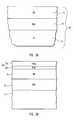
- FIG. 1Ais a cross-sectional view a high-resistivity bulk starting wafer.
- FIG. 1Bis a cross-sectional view of a low-resistivity bulk starting wafer, with a high-resistivity epitaxial layer deposited on top.
- FIG. 2Ais a cross-sectional view of a high-resistivity SOI starting wafer.
- FIG. 2Bis a cross-sectional view of the high-resistivity SOI starting wafer shown in FIG. 2A after pad 20 has been deposited on top.
- FIG. 3Ais a plan view of the device after trenches have been etched into the top silicon layer.
- FIG. 3Bis a cross sectional view taken along the width of the device after trenches have been etched into the top silicon layer.
- FIG. 3Cis a cross sectional view along the length of the device after trenches have been etched into the top silicon layer.
- FIG. 3Dis an isometric view of the device taken along cutting line 3 D after trenches have been etched into the top silicon layer.
- FIG. 4Ais a plan view of the device after a second silicon etch.
- FIG. 4Bis a cross sectional view taken along the width of the device after a second silicon etch.
- FIG. 4Cis a cross sectional view along the length of the device after a second silicon etch.
- FIG. 4Dis an isometric view of the device taken along cutting line 4 D after a second silicon etch.
- FIG. 5Ais a plan view of the device after mask 3 has been implanted.
- FIG. 5Bis a cross sectional view taken along the width of the device after mask 3 has been implanted.
- FIG. 5Cis a cross sectional view along the length of the device after mask 3 has been implanted.
- FIG. 5Dis an isometric view of the device taken along cutting line 5 D after mask 3 has been implanted.
- FIG. 6Ais a plan view of the device after formation of sidewall spacers and after implant 119 .
- FIG. 6Bis a cross sectional view taken along the width of the device after formation of sidewall spacers and after implant 119 .
- FIG. 6Cis a cross sectional view along the length of the device after formation of sidewall spacers and after implant 119 .
- FIG. 6Dis an isometric view of the device taken along cutting line 6 D after formation of sidewall spacers and after implant 119 .
- FIG. 7Ais a plan view of the device after the formation of a first gate conductor layer.
- FIG. 7Bis a cross sectional view taken along the width of the device after the formation of a first gate conductor layer.
- FIG. 7Cis a cross sectional view along the length of the device after the formation of a first gate conductor layer.
- FIG. 7Dis an isometric view of the device taken along cutting line 7 D after the formation of a first gate conductor layer.
- FIG. 8Ais a plan view of the device after application of top gate mask (mask 4 ).
- FIG. 8Bis a cross sectional view taken along the width of the device after application of top gate mask (mask 4 ).
- FIG. 8Cis a cross sectional view along the length of the device after application of top gate mask (mask 4 ).
- FIG. 8Dis an isometric view of the device taken along cutting line 8 D after application of top gate mask (mask 4 ).
- FIG. 9Ais a plan view of the device after the trenches have been refilled with isolation dielectric.
- FIG. 9Bis a cross sectional view taken along the width of the device after the trenches have been refilled with isolation dielectric.
- FIG. 9Cis a cross sectional view along the length of the device after the trenches have been refilled with isolation dielectric.
- FIG. 9Dis an isometric view of the device taken along cutting line 9 D after the trenches have been refilled with isolation dielectric.
- FIG. 10Ais a plan view of the device after the isolation dielectric has been patterned by local interconnect mask (mask 5 ).
- FIG. 10Bis a cross sectional view taken along the width of the device after the isolation dielectric has been patterned by local interconnect mask (mask 5 ).
- FIG. 10Cis a cross sectional view along the length of the device after the isolation dielectric has been patterned by local interconnect mask (mask 5 ).
- FIG. 10Dis an isometric view of the device taken along cutting line 10 D after the isolation dielectric has been patterned by local interconnect mask (mask 5 ).
- FIG. 11Ais a plan view of the device after the gate structure has been completed.
- FIG. 11Bis a cross sectional view along the width of the device after the gate structure has been completed.
- FIG. 11Cis a cross sectional view along the length of the device after the gate structure has been completed.
- FIG. 11Dis an isometric view of the device taken along cutting line 11 D after the gate structure has been completed.
- FIG. 12Ais a plan view of the device following conventional contact and second metal processing.
- FIG. 12Bis a cross sectional view along the width of the device following conventional contact and second metal processing.
- FIG. 12Cis cross sectional view along the length of the device following conventional contact and second metal processing.
- FIG. 12Dis an isometric view of the device taken along cutting line 12 D following conventional contact and second metal processing.
- FIG. 13Ais a plan view of device with contact holes misaligned.
- FIG. 13Bis a cross sectional view along the width of the device with contact holes misaligned.
- FIG. 13Cis a cross sectional view along the length of the device with contact holes misaligned.
- FIG. 13Dis an isometric view of the device taken along cutting line 13 D with contact holes misaligned.
- FIG. 14Ais provided for comparison to FIG. 14A and depicts a cross sectional view along the width of the device that is identical to FIG. 12B.
- FIG. 14Bschematically depicts the terminal connections of the device.
- FIG. 15Ashows the floating body configuration of the device.
- FIG. 15Bschematically depicts the terminal connections of the device.
- FIG. 16Ashows the dynamic threshold configuration of the device.
- FIG. 16Bschematically depicts a cross sectional view of the device showing the terminal connections of the device.
- FIG. 17Adepicts a cross sectional view of substrate of embodiment 100 ′′.
- FIG. 17B and FIG. 18are cross sectional views depicting embodiment 100 ′′ before and after etching.
- FIG. 19Adepicts a cross sectional view of the device after completion of the step of depositing and etching sidewall spacer for embodiment 100 ′′.
- FIG. 19Bdepicts a cross sectional view of the device after completion of the step of directing complementary, counter-doping ion implants for embodiment 100 ′′.
- FIG. 19Cdepicts a cross sectional view of the device after the step of directing complementary, counter-doping ion implants for embodiment 100 ′′.
- FIG. 20depicts a cross sectional view of the device after the step of depositing a gate dielectric for embodiment 100 ′′.
- FIG. 21depicts a cross sectional view of the device after the step of plasma etching first gate conductor for embodiment 100 ′′.
- FIG. 22Adepicts a cross sectional view along the width of the device after the step of filling isolation trenches along the channel length direction of embodiment 100 ′′.
- FIG. 22Bdepicts a cross sectional view along the length of the device the step of filling isolation trenches along the channel width direction of embodiment 100 ′′.
- FIG. 23Adepicts a cross sectional view along the width of the device after the step of etching oxide down to BOX layer 13 .
- FIG. 23Bdepicts a cross sectional view along the length of the device after the step of etching oxide down to BOX layer 13 .
- FIG. 24Adepicts a cross sectional view of the Damascene double gated transistor taken along the channel length direction.
- FIG. 24Bdepicts a cross sectional view of the Damascene double gated transistor taken along the channel width direction.
- FIG. 25Ais a cross sectional view of another embodiment of the Damascene double gated transistor.
- FIG. 25Bdepicts the doping profile in the channel and body/well of embodiment shown in FIG. 25A.
- FIGS. 2 - 12Several methods are disclosed herein for forming Damascene double gated transistors. Before explaining the steps of the method shown in FIGS. 2 - 12 that are used to achieve the final structure, it is useful to appreciate the configuration of the final structure shown in FIGS. 11 A-D and FIGS. 12 A-D. Another method is depicted in FIGS. 17 - 24 with the final structure shown in FIGS. 24 A- 24 B.
- FIG. 25Adepicts an additional embodiment.
- FIGS. 1 A- 1 B and 2 Adepict some of the various substrates that can be used in accordance with the inventive methods and structures.
- Substrate 10 shown in FIG. 1Ais bulk silicon 11 that preferably has a high resistivity such as 1 k ohm-cm. The resistivity may range from 100-10 k ohm-cm. Alternatively, a triple-well bulk silicon substrate may be used instead.
- Substrate 10 ′ shown in FIG. 1Bhas an epitaxial layer 12 on bulk silicon 11 ′ which has a low resistivity. The low resistivity of silicon 11 ′ may range from 0.1 to 10 ohm-cm.
- FIG. 2Adepicts a starting silicon-on-insulator (SOI) substrate 10 ′′.
- Layer 11is the silicon substrate.
- Substrate 10 ′′has a layer 13 that is under a SOI layer or wafer 14 and above silicon 11 .
- Layer 13is a buried insulator (typically silicon dioxide referred to as a BOX layer).
- the thickness of BOX layer 13may vary from several microns down to 100 nm, however, the thickness is preferably in a range from about 100 nm to about 500 nm.
- Layer 14is the thin crystalline silicon layer where devices are built.
- Layer or SOI wafer 14may be formed by any desirable available method such as SIMOX, SmartCut bonded, Metal-induced poly recrystallization, etc.
- Layer 14preferably has a high resistivity of 1 k ohm-cm.
- the initial crystalline SOI film thicknessmay be any available thickness but is preferably either thinned by etching or thickened by epi-growth to a range from about 200 nm to about 300 nm. Note that substrate 10 ′′ is particularly preferred for a RF-CMOS application.
- Another substrate 10 ′′′may also be utilized that has four layers.
- the surface layeris an epitaxial layer 12 ′.
- Epitaxial layer 12 ′preferably has a thickness in a range from about 100 nm to about 200 nm.
- Epitaxial layer 12 ′is on a layer of silicon 11 ′ that has a low resistivity and preferably a thickness of about 100 nm.
- Silicon layer 11 ′is on BOX layer 14 .
- BOX layer 14preferably has the same thickness range as BOX layer 14 described above in reference to substrate 10 ′′.
- BOX layer 14is on a bottom layer of silicon 11 ′ that has low resistivity, preferably about 10 ohm-cm.
- Pad 20preferably includes a silicon nitride layer 22 over a thin silicon oxide stress relief layer 24 .
- Pad 20is the silicon etch hard mask and the chemical-mechanical polish (CMP) stop layer.
- Silicon nitride (Si 3 N 4 ) layer 22may have a thickness ranging from about 50 nm to about 200 nm.
- Layer 22may be deposited or grown to be used as both a silicon etch hardmask and as a chemical-mechanical polish (CMP) stopping layer without an oxide layer.
- the oxide layer 24is a very thin layer of thermal oxide 24 .
- layer 24may have a thickness of about 20 to about 40 nm.
- Pad 20is formed from a different material than the dielectric materials that surround the gate, namely spacers 30 and cap 150 , which are discussed below.
- spacers 30 and cap 150comprise silicon dioxide.
- spacers 30 and cap 150comprise silicon nitride.
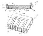
- FIGS. 3 - 12provide views of the various steps involve in forming the final Damascene double gated transistor referred to herein as device 100 throughout the description of the process.
- device 100the final Damascene double gated transistor referred to herein as device 100 throughout the description of the process.
- four viewsare provided including a plan view referenced by A, a cross-sectional view taken along the width of the device referenced by B, a cross-sectional view taken along the length of the device referenced by C and an isometric view of the device along cutting line 3 D in FIG. 3A.
- FIGS. 3 A-Dprovide various views of the device after the first masking/patterning step has been completed utilizing mask 1 .
- Merged gate trench 110 and isolation trench 112are etched into the top silicon layer, leaving a 50-200 nm thick silicon layer 14 remaining on BOX layer 13 .
- Note that the different portions of isolation trench 112are individually identified as 112 a - d .
- This maskis the union shape of typical CMOS Active Area & Gate masks.
- the silicon substrate layer 11 and BOX layer 13are omitted from the subsequent drawings for clarity, however, it should be understood that layer 14 remains on BOX layer 13 which is on silicon substrate layer 11 .
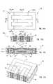
- FIGS. 4 A- 4 Dshow the result of the second mask identified as mask 2 , which protects the channel region 120 from a second silicon etch. This second etch removes the rest of the silicon from the bottom of the trenches 112 in the isolation regions around the channel, source, and drain, stopping on the BOX layer 13 .
- FIGS. 5 A-Dshows the results of two sets, one deep 117 and one shallow 118 , of masked, complementary ion implants utilizing mask 3 . These implants are used to form the source/drain junctions or regions and a channel region 120 .
- channel region 120has a counter doped channel layer or portion 122 and a remaining bottom intrinsic layer or portion 124 .
- the n+ regionscorrespond with the source and drain pedestals respectively identified in FIG. 5D as 114 s and 114 d .
- the p+ regionscorrespond with a surrounding p+ source/drain pedestal identified in FIG. 5D as 116 . Note that p+ source/drain pedestal 116 belongs to adjacent p+ devices so it is not a part of device 100 .
- the deep n+ implant 117may be a series of implants of various energies and doses in order to form a uniformly, heavily doped source/drain all the way down to the BOX layer 13 .
- the counter doped channel layer 122has a very abrupt profile in order to leave the bottom intrinsic layer 124 undoped, so heavy ion species are used such as Indium and Arsenic. Since BOX layer 13 and pad 20 are dielectrics, they permit use of these “shallow/deep” pair of implants. More particularly, because these regions are dielectric the dopants are implantable into these regions without significantly affecting the device structure or operation.
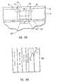
- FIGS. 6 A- 6 Dshows the formation of sidewall spacers 30 followed by a high-dose, relatively high-energy p+ implant 119 , such as Indium, that forms the buried low-resistance bottom gate 124 ′ of device 100 .
- sidewall spacers 30comprise silicon dioxide in this embodiment.
- bottom gate 124 ′is self-aligned to the bottom of the gate trench 110 between the two spacers 30 and these spacers 30 prevent bottom gate 124 ′ from abutting either the heavily-doped source or drain regions or pedestals 114 s and 114 d , leaving regions of bottom intrinsic layer 124 to the left and right of the bottom gate 124 ′ that are undoped or at least lightly doped. These intrinsic regions of bottom intrinsic layer 124 are identified with the letter i.
- FIGS. 7 A- 7 Ddepict the formation of a first gate conductor layer 130 over channel region 120 .
- a gate dielectric layer 128preferably having a high dielectric constant, such as hafnium oxide, underlies first gate conductor layer.
- all high temperature stepsare complete, meaning that temperature-sensitive materials, such as hafnium oxide and copper may respectively be used for the gate dielectric and conductor material.
- First gate conductor layer 130may be any suitable conductor material that enables the desired threshold voltage. Examples of suitable materials include tungsten, polysilicon, poly-SiGe or a silicide. As shown in FIG. 7D, the trenches 110 and 112 are overfilled with the material that forms the first gate conductor material 130 . The materials is then planarized back to the pad 20 , and then recessed, preferably by plasma etching, leaving about 50-200 nm of a first gate conductor layer 130 over the channel region 120 .
- FIGS. 8 A- 8 Dshows the results of the top gate mask, identified as mask 4 , being applied to the device.
- the entire channel 110 and gate stackis patterned and etched, stopping on the bottom gate layer 124 ′.
- Mask 4may fully or partially cover the bottom gate mask, which is mask 3 . Additionally, mask 4 may be offset to the left or right of the bottom gate mask, simultaneously creating four-terminal as discussed below in reference to FIGS. 14 A-B, floating body as discussed below in reference to FIGS. 15 A-B, and dynamic threshold devices as discussed below in reference to FIGS. 16 A-B.
- the final device length and widthare respectively identified in FIG. 8B at 1 and in FIG. 8C at w.
- FIGS. 9 A- 9 Dshows the trenches 110 and 112 refilled with isolation dielectric 40 .
- Isolation dielectricis preferably silicon dioxide. After the trenches 110 and 112 have been filled then the isolation dielectric 40 is planarized, as shown.
- FIGS. 10 A- 10 Dshows isolation dielectric 40 after it has been patterned by the local interconnect (LI or MO) mask identified as mask 5 .
- Mask 5is used to remove portions of isolation dielectric 40 in the isolation trenches 112 .
- FIGS. 11 A- 11 Dshow the completed gate structure.
- the second gate conductor materialis deposited in a manner such that the trench is overfilled. After being overfilled, the second gate conductor material is planarized and then recessed.
- the second gate conductor materialis preferably a metal.
- the resulting second gate conductor layer 140serves as a first interconnect or metal level.
- a first metal levelis used to locally wire the bottom and top gates to adjacent circuits and to create a zero-area DTMOS top gate-to-bottom gate connection.
- a cap 150is then formed.
- Cap 150is formed by refilling recessed top portions of the second gate conductor layer 140 with a dielectric such as silicon dioxide.
- Cap 150 or capping layerprevents contacts from subsequently shorting to the top of the M 0 metal, second gate conductor layer 140 .
- FIGS. 12 A- 12 Dshow device 100 following conventional contact and second metal processing.
- An interlevel dielectric 210also identified as ILD is deposited, followed by contact patterning and etching through this ILD 210 and through the pad dielectric 20 . This etch does not etch the cap 150 or isolation dielectric 40 .
- the contact holes 220are then filled with metal 222 and planarized, followed by deposition and patterning of second metal 224 .
- Dual Damascene processingcould be used for contact and second metal processing.
- FIGS. 12 A-Dshows the final completed device structure in a four-terminal configuration where the bottom gate is wired out to the left and the top gate is wired out to the right, the source is wire to the bottom and the drain is wire to the top.
- This configurationenables all four terminals 230 , 232 , 234 and 236 to be biased independently.
- FIGS. 13 A- 13 Dshow that even if contact holes 220 are misaligned the contact holes still provide a via between the second level of metal 224 and the pedestals 114 s or 114 d . Shorting is avoided as there is no connection to second gate conductor layer 140 , metal M 0 , due to the isolating configuration of cap 150 .
- FIG. 14Ais identical to FIG. 12B and is included for convenient comparison with FIG. 14B which schematically depict the terminal connections of the device. Note that the configuration shown in FIGS. 14A and 12B is enabled through the offset positioning of masks 3 and 4 .
- FIG. 15Ashows the floating body configuration of this device, where the bottom gate is electrically isolated by the spacers and gate dielectric from the top gate or M 0 .
- Top gateencloses the bottom gate due to the use of top gate mask that is larger than the bottom gate mask.
- FIG. 15Bschematically depicts the terminal connections of the device.
- FIG. 16Ashows the dynamic threshold (DTMOS) configuration of this device, where the top and bottom gates are shorted at both the left and right sides of the channel.
- Bottom gateencloses the top gate due to the use of a bottom gate mask that is larger than the top gate mask.
- FIG. 16Bschematically depict the terminal connections of the device.
- FIGS. 17 - 24depict another embodiment for forming a Damascene double gate transistor.
- FIG. 17Adepicts a substrate like that shown in FIG. 2B with a pad 20 on substrate 10 ′′.
- the source/drain implantsare formed before etching the trenches. The doping may be followed by rapid thermal activation. The depth of these top-side junctions can be adjusted as needed for subsequent silicidation and sheet resistance, without impacting the short-channel behavior of the device. Since these source and drain regions will effectively be “raised” with respect to the channel, they may be made thicker and lower in resistance than typical CMOS processes.
- FIG. 17Bdepicts device 100 ′′ after gate trench 110 and isolation trench 112 have been formed.
- This first photolithography leveldefines the source and drain regions of the device.
- the etchingis preferably a silicon plasma etch.
- About 100 nm of SOI filmis preferably left under these trenches, as shown in the sideview in FIG. 17B.
- FIG. 18shows the formation of a doped channel layer or portion 122 ′.
- Doped channel layer 122 ′may be formed by any suitable method.
- layer 122may be formed through the use of large angle tilted implantation or alternatively through the use of dummy doping with a sacrificial layer that is subsequently removed.
- complementary high-dose, low-energy, large-angle-tilted ion implantsare performed to form the trench sidewall and bottom S/D junctions.
- Indiumcan be used for P-channel and arsenic for N-channel devices, followed by rapid thermal activation.
- Sidewall junctionsare preferably made shallow to control short channel effects.
- An optional thin sacrificial oxidecan be performed to remove any plasma etch or implantation damage from the bottom of the trench where the channel will be and to prevent any stress damage from the coming nitride sidewall spacers 30 .
- nitride sidewall spacers 30are then deposited and etched, providing an opportunity for optional halo (not shown) and S/D extension implants before and/or after the spacer formation.
- Nitride sidewall spacers 30are preferably about 20 nm thick. Spacers 30 also protect the S/D regions from subsequent shorting to the gate during the gate to body contact process. Anisotropic etching may be used to remove the Si 3 N 4 from the top surface and the bottom of the gate.
- complementary, counter-doping ion implantsare preferably then directed into the open bottom of gate trench 110 between the sidewall spacers 30 .
- high-dose, higher-energy implantspreferably indium for N-channel and preferably arsenic for P-channel
- these high-dose, higher-energy implantscompensate the previous shallow S/D implants, resulting in low net doping down into the body in a range of about 30 nm to about 50 nm where the inversion channel will be located, with a hyper-abrupt transition to high concentration in the bottom portion of the body where the body contact will be formed and body current conducted.
- the resulting configurationis shown in FIG. 19C with the p+ region indicated at 124 ′.
- the resulting heavily doped body “stripe”is self-aligned to the future gate “stripe” directly above it but not underneath the S/D regions, thus minimizing capacitance.
- the counter-dopingcan be achieved by doping from ion implantation with or without tilt for symmetrical or asymmetrical structures. Counterdoping can also be achieved through solid source doping from a sacrificial layer.
- the implantis preferably indium for the N-channel and preferably arsenic for the P-channel devices.
- the resulting doping profile in the channel and body/wellis shown in FIG. 25B, as discussed below. Advantages of the hyper-abrupt retrograde profile below the channel achieved through the critical body counter-doping ion implantation are explained below after the overall method has been fully set forth.
- a gate dielectric 128is deposited as shown in FIG. 20.
- Any appropriate gate dielectricmay be used including temperature-sensitive high-k dielectrics such as hafnium oxide.
- Deposition of the gate dielectricis followed by a trench-filling deposition of the first gate conductor material 130 .
- First gate conductor material 130is preferably either doped or undoped polysilicon or a polysilicon-germanium alloy where the percent germanium content is used to adjust the gate workfimction and therefore the device threshold voltage.
- First gate conductor material 130may also be a metal such as tungsten or titanium nitride. Chemical-mechanical polish (CMP) of this layer back to the pad then follows.
- CMPChemical-mechanical polish
- First gate conductor material 130is plasma-etch recessed to about 30 nm in the trench bottom, followed by an optional temporary oxide trench fill deposition and CMP, as shown in FIG. 21.
- Isolation trenches 112are then filled with oxide 40 , as is the region above first gate conductor material 130 , and planarized back to nitride pad 20 , resulting in the sideviews shown in FIGS. 22A.
- FIG. 22Adepicts the channel length direction
- FIG. 22Bshows the channel width direction, including the endwall where the first gate conductor material 130 will be shorted to the retrograde body implant 122 by the upcoming second gate conductor material 140 .
- FIGS. 23 A- 23 Bdepict the resulting configuration in views that are respectively, the channel length direction and the channel width direction.
- FIG. 23Bdepicts the removal of oxide 40 down to BOX layer 13 .
- FIG. 23Adepicts the removal down to first gate conductor material 130 .
- This M 0 trenchis filled with the second gate material 140 (by deposition of a low-resistance metal such as copper or other suitable material, and then planarizing by a process such as CMP.
- Second gate material 140is positioned to short the top and ends of the first gate conductor material 130 to the buried heavily doped body at both endwalls of the device, but does not short to the S/D implants due to the protecting nitride sidewall spacers.
- This second gate conductor material 140is plasma recessed to a thickness of about 30 nm and then capped with an oxide fill 150 and then planarized.
- the resulting final transistor structureis completely planar, as shown in FIG. 24A.
- the zero-area, zero-capacitance endwall gate-body DTMOS connectionis identified in FIG. 24B at 70 .
- a standard CMOS multi-level, dual-Damascene metal interconnect processis then completed, like that shown in FIGS. 12 A- 12 D. Notice that the spacing of S/D metal contacts to the gate and to each other is reduced compared to prior art device. This condensed configuration increases layout density without causing S/D to gate shorts due to the tolerance of the structure to misalignment. These contacts can be “borderless” since they are self-aligned to the gate cap insulator. This improves the density of memory cells such as compact DRAM, SRAM, and FLASH cell designs.
- Such processesinvolve building a dummy poly gate and sidewall spacers, performing all S/D implants and anneals, planarizing the structure with a CMP polish insulator, removing the dummy gate, depositing a high k gate dielectric and a low resistance gate metal, and then planarizing the surface to leave a Damascene metal gate in the groove where the dummy poly gate had been.
- Disadvantages of such processinclude a high S/D resistance due to shallow S/D junctions or the S/D contacts being non self-aligned to the gate.
- the first problemis particularly relevant to sub-100 nm devices and the second problem is particularly relevant to compact DRAM, SRAM and FLASH cells.
- the present inventionis a Damascene metal “gate last” process that results in effectively raised source/drain regions for reduced S/D resistance.
- the inventive processalso provides self-aligned, borderless S/D contacts that will not short the gate even with a complete overlap.
- Another advantage of the inventive methodis the elimination of the wells typically formed bulk silicon by conventional implementations of DTMOS.
- Current DTMOS implementationsrequire a “triple-well” structure with a shallow N-well, shallow P-well and a deep N-well to isolate individual body nodes from each other.
- the present methodeliminates this well processing and is accordingly referred to as “Well-less CMOS”.
- the well-less CMOS methodologyresults in sufficient isolation by using high resistivity epitaxial isolation coupled with sub-volt biases and optional VDD/2 epi substrate bias.
- the novel bulk silicon “semi-insulating” substrate designwill also decrease the cross-talk, noise coupling, and passive component Q losses typical of existing bulk CMOS processes.
- FIG. 25Ais a side view of a transistor that has a counter doped region that was formed by a different method than that set forth above in relation to FIGS. 17 - 24 .
- the surface of the substrateis first doped and the trench is formed on top of the substrate by depositing the insulative material around a dummy material that is subsequently removed. After removal of the dummy material then the spacers are deposited in preparation for counter-doping the bottom of the trench. After the counter-doping has been achieved then the subsequently layers can be deposited.
- novel hyper-abrupt retrograde well structureformed by counter-doping a preexisting S/D implant only in and below the channel region, enables the channel to be self-aligned and prevents contacts with the source/drain junctions.
- Such novel structuresare especially beneficial to bulk silicon implementations as it achieves most of the benefits of SOI DTMOS implementations.
- FIG. 25Billustrates the hyper-retrograde doping profile achieved in the substrate and the depth of the different layers of the transistor above the counter-doped region.
- FIG. 25Bis shown as depicting the profile for the device shown in FIG. 25A, however, the same profile results for the devices shown in FIGS. 11B and 24A.
Landscapes
- Engineering & Computer Science (AREA)
- Physics & Mathematics (AREA)
- Condensed Matter Physics & Semiconductors (AREA)
- General Physics & Mathematics (AREA)
- Manufacturing & Machinery (AREA)
- Computer Hardware Design (AREA)
- Microelectronics & Electronic Packaging (AREA)
- Power Engineering (AREA)
- Insulated Gate Type Field-Effect Transistor (AREA)
- Metal-Oxide And Bipolar Metal-Oxide Semiconductor Integrated Circuits (AREA)
- Internal Circuitry In Semiconductor Integrated Circuit Devices (AREA)
- Thin Film Transistor (AREA)
Abstract
Description
- This utility application claims priority to U.S. Provisional Application Serial No. 60/229,552 filed Aug. 29, 2000, which was filed by Stephen A. Parke, Ph.D. and Serial No. 60/287,226 filed on Apr. 27, 2001, which was also filed by Stephen A. Parke, Ph.D. Serial No. 60/229,552 and Serial No. 60/287,226 are hereby incorporated by reference.[0001]
- This invention relates generally to transistors. More particularly, this invention relates to a transistor that is fully planar and operates at low voltages.[0002]
- The shrinking of silicon-based CMOS transistors from 10 um to sub-100 nm channel lengths has been the driving force behind the incredible advances in integration density of digital circuits. This exponential growth in circuit density (Moore's Law) has enabled increasingly sophisticated and fast microprocessors and digital signal processors. However, in this “post-PC age”, the markets driving the semiconductor industry are handheld consumer electronics, wireless communications, and Internet infrastructure. The ITRS Roadmap for the next ten years calls as much or more for increased diversity of integrated functions as for increased density.[0003]
- CMOS switching frequencies (f[0004]T) exceeding 150 GHz have recently been achieved. Because this high-performance can be achieved using a relatively low cost manufacturing process, CMOS is rapidly becoming a serious option for many wireless Radio Frequency (RF) applications that were previously considered to be the exclusive domain of more expensive technologies, such as bipolar and gallium arsenide. This has led to a research focus shift to highly-integrated, highly-diverse CMOS System-On-a-Chip (SOC) technologies, integrating entire wireless mixed-signal systems on a single chip. Innovative device and technology changes are needed to provide high quality passive elements and high-gain, high-linearity, low-noise, low-power, RF capable transistors on carefully engineered substrates which reduce coupling and crosstalk noise of digital circuits from affecting sensitive on-chip RF receivers.
- RF SOC's with the lowest possible energy consumption will use advanced spread-spectrum communication algorithms. Current research spans the circuit, architecture, and algorithm issues which impact the design of SOC CMOS wireless transceivers. Research activities also span bulk Si, SiGe, and SOI deep-sub-micron CMOS designs, the design of analog RF front ends, the design of A/D interface circuitry, and digital baseband signal processing. However, it is clear that single chip RF SOC solutions will require more than simply innovative circuit designs in order to be optimized.[0005]
- The most serious limitation of these portable SOCs is power dissipation. The system battery typically comprises a large percentage of the cost, size, weight, and reliability problems in current handheld RF devices. As these systems become more highly integrated by utilizing sub-100 nm RF-CMOS devices, the power dissipation will become an even greater concern. Therefore, in order for the low-cost and high-integration density of RF-CMOS to be fully realized, it is imperative that new ultra-low power device structures and circuit design techniques be developed. These devices should preferably maintain multi-GHz level performance while operating with power supply voltages down to 0.25 volts. They also should preferably maintain high transconductance and low noise, and be easily integrated with on-chip, high-Q, tunable passive elements such as spiral inductors.[0006]
- In summary, there is a need in the art for devices that operate at ultra low power. There is a need in the art for innovative transistors that provide for increased density. Additionally, there is a need to simplify the process for manufacturing transistors. Finally, there is a need to reduce the cost of manufacturing transistors.[0007]
- An object of the present invention is provide unique transistors that enable increased density. Another object of the present invention is provide transistors that operate at ultra low power. An additional object of the present invention is to simplify the process for manufacturing transistors. Finally, an object is to reduce the cost of manufacturing transistors.[0008]
- The above and other objects and advantages, which will be apparent to one of skill in the art, are achieved in the present invention which is directed to, in the first aspect, a method of manufacturing a Damascene double gated transistor, and the structure made by the method. More particularly, the invention provides a method for simultaneously making both four-terminal and dynamic threshold MOSFET devices. The method starts with either 1) a high-resistivity bulk silicon substrate (with or without an epitaxial layer) or a silicon-on-insulator substrate or similar substrate having an isolated semiconductor region defined on its surface. These substrates may be created by any of the existing methods for making 1)high-resistivity bulk silicon or 2) SOI i.e. SIMOX, BESOI, SmartCut, Metal-induced recrystallization, Laser-induced recrystallization, etc.[0009]
- In one embodiment, a silicon trench etch hard mask and polish stop “pad” layer (e.g. silicon nitride) is first deposited on the top silicon layer. A merged isolation/gate trench is then etched partially through this top silicon layer. A second mask and etch are used to completely remove the remaining silicon from the bottom of the isolation trenches, while leaving a thin active region of silicon under the gate trench which will become the channel. The remaining silicon “island” is barbell shaped, with large, thick source/drain regions on either side of the narrow, thin channel region. The gate trench is used for subsequently forming the bottom gate, channel, and top gate which are all self-aligned to this trench opening. A complementary set of shallow and deep implants is used to form a counter-doped channel and to heavily, uniformly dope the source/drain regions, respectively. This counter-doped channel is especially useful for maximizing the dynamic threshold swing, since it enhances body effect. Sidewall spacer material is then deposited, both to narrow the gate opening for sub-lithographic channel length and to isolate the sidewalls of the source/drain regions. Following the spacer formation, a highly-doped buried bottom gate is formed by ion implantation. This implant is masked by both the pad and the spacers, which space it away from both the heavily doped source and drain regions to prevent leakage and capacitance. The energy of this implant is high enough to place it below the counter-doped channel layer. High atomic weight ions are used (Indium for p+ and arsenic for n+) in order to obtain a super-steep retrograde implant profile between this buried layer and the channel above. Optionally, a thin undoped selective epitaxial silicon layer may be grown on top of the counter-doped channel to enhance the mobility of the device. At this point in the process, all high temperature steps are complete, meaning that temperature-sensitive materials (such as hafnium oxide and copper) may be used for the gate stack. Polysilicon or polysilicon/germaninum with an adjustable percentage of Ge may be used as the first gate conductor layer, in order to achieve additional threshold voltage design control. Alternately, a metal or silicide may also be used for the first gate conductor layer. The isolation/gate trenches are overfilled with this first gate conductor material, planarized back to the pad layer, and plasma recessed. Next, the entire channel and gate stack is patterned and etched, stopping on the bottom gate layer. The alignment of this mask to the original channel mask determines whether the resulting device is four-terminal, DTMOS, or floating body. All three types of devices are fabricated simultaneously on the same substrate and may be used as needed for various circuit applications. Next, the trenches are refilled with isolation dielectric (e.g. silicon dioxide) and planarized. This trench dielectric is then patterned and etched out in order to form a “Damascene” metal local interconnect (LI or M[0010]0) for wiring the top and bottom gates to adjacent circuits. This metal (second gate conductor) is deposited to overfill the trenches, planarized back to the pad layer, and plasma recessed slightly. This recess is then filled with a “cap” dielectric (e.g. silicon dioxide) and planarized. This cap prevents the subsequent contact etch from reaching the buried local interconnect metal. Finally, an interlevel dielectric is deposited and either plasma etched or Dual-Damascene metal one and contact one levels are patterned, etched, filled and planarized. The contact etch is selective, penetrating the pad dielectric in order to contact the top of the junctions, but not penetrating the trench cap dielectric. Thus the source/drain contacts are self-aligned with respect to the gate and isolation regions. Typical interconnect processing is used for all subsequent levels.
- This invention describes the structure and fabrication process of a novel completely planar, DTMOS device structure which overcomes several key existing problems and extends the DTMOS advantages to both bulk and SOI sub-100 nm CMOS technologies. This process permits easy incorporation of high-K gate dielectrics, such as tantalum pentoxide, and low resistance metal gates, such as copper, with a novel self-aligned, hyper-abrupt retrograde body implant. Current drive/speed, power-delay product, transconductance, output resistance, linearity, noise, hot-electron reliability, and device threshold matching are all superior to existing MOSFET designs. This invention's applications are far-reaching, but are particularly enabling for 0.25V-1.0V mixed-signal & RF CMOS SOC building block circuits. Between the large power supply reduction and superior analog/RF performance, order of magnitude power reductions can be achieved with this approach. This invention's application primary focus is on highly integrated CMOS system-on-a-chip (SOC) implementations, which have the lowest possible energy consumption while using advanced spread-spectrum communication algorithms. This includes multi-GHz wireless transceivers. Applications span bulk and SOI deep-sub-micron (DSM) and sub-100 nm CMOS technologies. It is expected that the application of this invention will permit single-chip digital pico-radios capable of supporting a wide variety of data types ranging from low bandwidth data, control, voice, and text messaging, up to full streaming video in a variety of pocket and handheld devices.[0011]
- In one embodiment, a DTMOS structure comprises a silicon transistor in which the gate is constructed of two conducting layers and a capping insulating layer that are all embedded in a groove etched into the original SOI or epitaxial silicon layer. The result is a completely planar structure with low gate, body, and S/D resistances. Both the sequence of process steps and the resulting transistor structure are novel. The gate layers are all deposited after the high-temperature source/drain processing is complete, thus protecting them from possible high-temperature damage. A compact, low capacitance endwall (sometimes referred to as a sidewall) contact is formed between the top gate material and the self-aligned hyper-abrupt retrograde body. In one embodiment, this structure is built on a high-resistivity SOI wafer. In another embodiment, it is built on high-resistivity epitaxial bulk silicon wafers, permitting the typical triple well processing to be eliminated. These devices can also be integrated with conventional CMOS devices (non-DTMOS) on the same chip to achieve tradeoffs.[0012]
- A novel zero-area, zero capacitance, low-resistance endwall contact is formed between the gate second layer and the buried low-resistance hyper-retrograde body region. The invention also provides a new hyper-abrupt retrograde well structure formed by counter-doping a pre-existing S/D implant only in and below the channel region, which is self-aligned to the channel and does not touch the source/drain junctions. This structure especially benefits bulk silicon implementation of DTMOS, achieving most of the benefits of SOI DTMOS implementations.[0013]
- This invention further provides a method for eliminating conventional well processing (Well-less CMOS), while maintaining sufficient isolation, by using high-resistivity epitaxial isolation coupled with sub-volt biases (and optional VDD/2 epi substrate bias), thereby dramatically reducing the complexity/cost of bulk silicon DTMOS implementations. This bulk silicon “semi-insulating” substrate design also decreases the cross-talk, noise coupling, and passive component Q losses typical of existing bulk CMOS processes.[0014]
- Conventional DTMOS processes typically include a typical plasma-etched polysilicon gate process, which leads to a highly-non-planar gate stack, high-resistance gate stack, plasma etch damage to the gate oxide, depletion of the poly gate, boron penetration through the gate dielectric, and incompatibility with high-temperature-intolerant gate stack materials. This last problem is due to the source/drain implant thermal processing, which usually follows the gate formation, leading to this process flow being labeled “gate first”. The processes disclosed herein includes a novel “recessed-channel” type of Damascene metal “gate-last” process that results in effectively raised source/drain regions for reduced S/D resistance. The processes also result in a novel dielectrically-capped, planar gate that permits self-aligned, borderless S/D contacts that will not short the gate even with complete overlap.[0015]
- Additional aspects and advantages of this invention will be apparent from the following detailed description of preferred embodiments thereof, which proceeds with reference to the accompanying drawings.[0016]
- FIG. 1A is a cross-sectional view a high-resistivity bulk starting wafer.[0017]
- FIG. 1B is a cross-sectional view of a low-resistivity bulk starting wafer, with a high-resistivity epitaxial layer deposited on top.[0018]
- FIG. 2A is a cross-sectional view of a high-resistivity SOI starting wafer.[0019]
- FIG. 2B is a cross-sectional view of the high-resistivity SOI starting wafer shown in FIG. 2A after[0020]
pad 20 has been deposited on top. - FIG. 3A is a plan view of the device after trenches have been etched into the top silicon layer.[0021]
- FIG. 3B is a cross sectional view taken along the width of the device after trenches have been etched into the top silicon layer.[0022]
- FIG. 3C is a cross sectional view along the length of the device after trenches have been etched into the top silicon layer.[0023]
- FIG. 3D is an isometric view of the device taken along cutting line[0024]3D after trenches have been etched into the top silicon layer.
- FIG. 4A is a plan view of the device after a second silicon etch.[0025]
- FIG. 4B is a cross sectional view taken along the width of the device after a second silicon etch.[0026]
- FIG. 4C is a cross sectional view along the length of the device after a second silicon etch.[0027]
- FIG. 4D is an isometric view of the device taken along cutting[0028]
line 4D after a second silicon etch. - FIG. 5A is a plan view of the device after[0029]
mask 3 has been implanted. - FIG. 5B is a cross sectional view taken along the width of the device after[0030]
mask 3 has been implanted. - FIG. 5C is a cross sectional view along the length of the device after[0031]
mask 3 has been implanted. - FIG. 5D is an isometric view of the device taken along cutting line[0032]5D after
mask 3 has been implanted. - FIG. 6A is a plan view of the device after formation of sidewall spacers and after[0033]
implant 119. - FIG. 6B is a cross sectional view taken along the width of the device after formation of sidewall spacers and after[0034]
implant 119. - FIG. 6C is a cross sectional view along the length of the device after formation of sidewall spacers and after[0035]
implant 119. - FIG. 6D is an isometric view of the device taken along cutting[0036]
line 6D after formation of sidewall spacers and afterimplant 119. - FIG. 7A is a plan view of the device after the formation of a first gate conductor layer.[0037]
- FIG. 7B is a cross sectional view taken along the width of the device after the formation of a first gate conductor layer.[0038]
- FIG. 7C is a cross sectional view along the length of the device after the formation of a first gate conductor layer.[0039]
- FIG. 7D is an isometric view of the device taken along cutting line[0040]7D after the formation of a first gate conductor layer.
- FIG. 8A is a plan view of the device after application of top gate mask (mask[0041]4).
- FIG. 8B is a cross sectional view taken along the width of the device after application of top gate mask (mask[0042]4).
- FIG. 8C is a cross sectional view along the length of the device after application of top gate mask (mask[0043]4).
- FIG. 8D is an isometric view of the device taken along cutting[0044]
line 8D after application of top gate mask (mask4). - FIG. 9A is a plan view of the device after the trenches have been refilled with isolation dielectric.[0045]
- FIG. 9B is a cross sectional view taken along the width of the device after the trenches have been refilled with isolation dielectric.[0046]
- FIG. 9C is a cross sectional view along the length of the device after the trenches have been refilled with isolation dielectric.[0047]
- FIG. 9D is an isometric view of the device taken along cutting[0048]
line 9D after the trenches have been refilled with isolation dielectric. - FIG. 10A is a plan view of the device after the isolation dielectric has been patterned by local interconnect mask (mask[0049]5).
- FIG. 10B is a cross sectional view taken along the width of the device after the isolation dielectric has been patterned by local interconnect mask (mask[0050]5).
- FIG. 10C is a cross sectional view along the length of the device after the isolation dielectric has been patterned by local interconnect mask (mask[0051]5).
- FIG. 10D is an isometric view of the device taken along cutting line[0052]10D after the isolation dielectric has been patterned by local interconnect mask (mask5).
- FIG. 11A is a plan view of the device after the gate structure has been completed.[0053]
- FIG. 11B is a cross sectional view along the width of the device after the gate structure has been completed.[0054]
- FIG. 11C is a cross sectional view along the length of the device after the gate structure has been completed.[0055]
- FIG. 11D is an isometric view of the device taken along cutting line[0056]11D after the gate structure has been completed.
- FIG. 12A is a plan view of the device following conventional contact and second metal processing.[0057]
- FIG. 12B is a cross sectional view along the width of the device following conventional contact and second metal processing.[0058]
- FIG. 12C is cross sectional view along the length of the device following conventional contact and second metal processing.[0059]
- FIG. 12D is an isometric view of the device taken along cutting line[0060]12D following conventional contact and second metal processing.
- FIG. 13A is a plan view of device with contact holes misaligned.[0061]
- FIG. 13B is a cross sectional view along the width of the device with contact holes misaligned.[0062]
- FIG. 13C is a cross sectional view along the length of the device with contact holes misaligned.[0063]
- FIG. 13D is an isometric view of the device taken along cutting[0064]
line 13D with contact holes misaligned. - FIG. 14A is provided for comparison to FIG. 14A and depicts a cross sectional view along the width of the device that is identical to FIG. 12B.[0065]
- FIG. 14B schematically depicts the terminal connections of the device.[0066]
- FIG. 15A shows the floating body configuration of the device.[0067]
- FIG. 15B schematically depicts the terminal connections of the device.[0068]
- FIG. 16A shows the dynamic threshold configuration of the device.[0069]
- FIG. 16B schematically depicts a cross sectional view of the device showing the terminal connections of the device.[0070]
- FIG. 17A depicts a cross sectional view of substrate of[0071]
embodiment 100″. - FIG. 17B and FIG. 18 are cross sectional[0072]
views depicting embodiment 100″ before and after etching. - FIG. 19A depicts a cross sectional view of the device after completion of the step of depositing and etching sidewall spacer for[0073]
embodiment 100″. - FIG. 19B depicts a cross sectional view of the device after completion of the step of directing complementary, counter-doping ion implants for[0074]
embodiment 100″. - FIG. 19C depicts a cross sectional view of the device after the step of directing complementary, counter-doping ion implants for[0075]
embodiment 100″. - FIG. 20 depicts a cross sectional view of the device after the step of depositing a gate dielectric for[0076]
embodiment 100″. - FIG. 21 depicts a cross sectional view of the device after the step of plasma etching first gate conductor for[0077]
embodiment 100″. - FIG. 22A depicts a cross sectional view along the width of the device after the step of filling isolation trenches along the channel length direction of[0078]
embodiment 100″. - FIG. 22B depicts a cross sectional view along the length of the device the step of filling isolation trenches along the channel width direction of[0079]
embodiment 100″. - FIG. 23A depicts a cross sectional view along the width of the device after the step of etching oxide down to[0080]
BOX layer 13. - FIG. 23B depicts a cross sectional view along the length of the device after the step of etching oxide down to[0081]
BOX layer 13. - FIG. 24A depicts a cross sectional view of the Damascene double gated transistor taken along the channel length direction.[0082]
- FIG. 24B depicts a cross sectional view of the Damascene double gated transistor taken along the channel width direction.[0083]
- FIG. 25A is a cross sectional view of another embodiment of the Damascene double gated transistor.[0084]
- FIG. 25B depicts the doping profile in the channel and body/well of embodiment shown in FIG. 25A.[0085]
- In describing an embodiment of the present invention, reference will be made in the drawings to elements of an embodiment by numerals that refer to like elements in another embodiment of the invention. Note that features of the invention are not necessarily shown to scale in the drawings. The device is described and drawn in an N-channel configuration, but the process provides complementary implants to simultaneously build P-channel devices as well.[0086]
- Several methods are disclosed herein for forming Damascene double gated transistors. Before explaining the steps of the method shown in FIGS.[0087]2-12 that are used to achieve the final structure, it is useful to appreciate the configuration of the final structure shown in FIGS.11A-D and FIGS.12A-D. Another method is depicted in FIGS.17-24 with the final structure shown in FIGS.24A-24B. FIG. 25A depicts an additional embodiment.
- FIGS.[0088]1A-1B and2A depict some of the various substrates that can be used in accordance with the inventive methods and structures.
Substrate 10 shown in FIG. 1A isbulk silicon 11 that preferably has a high resistivity such as 1 k ohm-cm. The resistivity may range from 100-10 k ohm-cm. Alternatively, a triple-well bulk silicon substrate may be used instead.Substrate 10′ shown in FIG. 1B has anepitaxial layer 12 onbulk silicon 11′ which has a low resistivity. The low resistivity ofsilicon 11′ may range from 0.1 to 10 ohm-cm. - FIG. 2A depicts a starting silicon-on-insulator (SOI)[0089]
substrate 10″.Layer 11 is the silicon substrate.Substrate 10″ has alayer 13 that is under a SOI layer orwafer 14 and abovesilicon 11.Layer 13 is a buried insulator (typically silicon dioxide referred to as a BOX layer). The thickness ofBOX layer 13 may vary from several microns down to 100 nm, however, the thickness is preferably in a range from about 100 nm to about 500 nm.Layer 14 is the thin crystalline silicon layer where devices are built. Layer orSOI wafer 14 may be formed by any desirable available method such as SIMOX, SmartCut bonded, Metal-induced poly recrystallization, etc.Layer 14 preferably has a high resistivity of 1 k ohm-cm. The initial crystalline SOI film thickness may be any available thickness but is preferably either thinned by etching or thickened by epi-growth to a range from about 200 nm to about 300 nm. Note thatsubstrate 10″ is particularly preferred for a RF-CMOS application. - Another[0090]
substrate 10′″ (not shown) may also be utilized that has four layers. The surface layer is anepitaxial layer 12′.Epitaxial layer 12′ preferably has a thickness in a range from about 100 nm to about 200 nm.Epitaxial layer 12′ is on a layer ofsilicon 11′ that has a low resistivity and preferably a thickness of about 100 nm.Silicon layer 11′ is onBOX layer 14.BOX layer 14 preferably has the same thickness range asBOX layer 14 described above in reference tosubstrate 10″.BOX layer 14 is on a bottom layer ofsilicon 11′ that has low resistivity, preferably about 10 ohm-cm. - As shown in FIG. 2B, once an appropriate substrate such as[0091]
substrate 10″ has been obtained then thepad 20 is formed.Pad 20 preferably includes asilicon nitride layer 22 over a thin silicon oxide stress relief layer24.Pad 20 is the silicon etch hard mask and the chemical-mechanical polish (CMP) stop layer. Silicon nitride (Si3N4)layer 22 may have a thickness ranging from about 50 nm to about 200 nm.Layer 22 may be deposited or grown to be used as both a silicon etch hardmask and as a chemical-mechanical polish (CMP) stopping layer without an oxide layer. The oxide layer24 is a very thin layer of thermal oxide24. For example layer24 may have a thickness of about 20 to about 40 nm. - [0092]
Pad 20 is formed from a different material than the dielectric materials that surround the gate, namely spacers30 andcap 150, which are discussed below. For a pad that comprises asilicon nitride layer 22 over a thin silicon oxide stress relief layer24,spacers 30 andcap 150 comprise silicon dioxide. Conversely, for apad 20 that comprises merely silicon dioxide, spacers30 andcap 150 comprise silicon nitride. - FIGS.[0093]3-12 provide views of the various steps involve in forming the final Damascene double gated transistor referred to herein as
device 100 throughout the description of the process. At each step, four views are provided including a plan view referenced by A, a cross-sectional view taken along the width of the device referenced by B, a cross-sectional view taken along the length of the device referenced by C and an isometric view of the device along cutting line3D in FIG. 3A. - FIGS.[0094]3A-D provide various views of the device after the first masking/patterning step has been completed utilizing
mask 1.Merged gate trench 110 andisolation trench 112 are etched into the top silicon layer, leaving a 50-200 nmthick silicon layer 14 remaining onBOX layer 13. Note that the different portions ofisolation trench 112 are individually identified as112a-d. This mask is the union shape of typical CMOS Active Area & Gate masks. Thesilicon substrate layer 11 andBOX layer 13 are omitted from the subsequent drawings for clarity, however, it should be understood thatlayer 14 remains onBOX layer 13 which is onsilicon substrate layer 11. - FIGS.[0095]4A-4D show the result of the second mask identified as
mask 2, which protects thechannel region 120 from a second silicon etch. This second etch removes the rest of the silicon from the bottom of thetrenches 112 in the isolation regions around the channel, source, and drain, stopping on theBOX layer 13. - FIGS.[0096]5A-D shows the results of two sets, one deep117 and one shallow118, of masked, complementary ion
implants utilizing mask 3. These implants are used to form the source/drain junctions or regions and achannel region 120. As discussed below,channel region 120 has a counter doped channel layer orportion 122 and a remaining bottom intrinsic layer orportion 124. The n+ regions correspond with the source and drain pedestals respectively identified in FIG. 5D as114sand114d. The p+ regions correspond with a surrounding p+ source/drain pedestal identified in FIG. 5D as116. Note that p+ source/drain pedestal 116 belongs to adjacent p+ devices so it is not a part ofdevice 100. - The[0097]
deep n+ implant 117 may be a series of implants of various energies and doses in order to form a uniformly, heavily doped source/drain all the way down to theBOX layer 13. The counter dopedchannel layer 122 has a very abrupt profile in order to leave the bottomintrinsic layer 124 undoped, so heavy ion species are used such as Indium and Arsenic. SinceBOX layer 13 andpad 20 are dielectrics, they permit use of these “shallow/deep” pair of implants. More particularly, because these regions are dielectric the dopants are implantable into these regions without significantly affecting the device structure or operation. - FIGS.[0098]6A-6D shows the formation of
sidewall spacers 30 followed by a high-dose, relatively high-energy p+ implant 119, such as Indium, that forms the buried low-resistance bottom gate 124′ ofdevice 100. Note thatsidewall spacers 30 comprise silicon dioxide in this embodiment. It should be noted that thebottom gate 124′ is self-aligned to the bottom of thegate trench 110 between the twospacers 30 and thesespacers 30 preventbottom gate 124′ from abutting either the heavily-doped source or drain regions or pedestals114sand114d, leaving regions of bottomintrinsic layer 124 to the left and right of thebottom gate 124′ that are undoped or at least lightly doped. These intrinsic regions of bottomintrinsic layer 124 are identified with the letter i. - FIGS.[0099]7A-7D depict the formation of a first
gate conductor layer 130 overchannel region 120. Agate dielectric layer 128, preferably having a high dielectric constant, such as hafnium oxide, underlies first gate conductor layer. Additionally, it is preferable to form a thin undoped selective epitaxial silicon layer on top of thecounter-doped channel layer 122 to enhance the mobility of the device as shown in FIGS.7B-7C at126 before forming thegate dielectric layer 128 and firstgate conductor layer 130. After the selectiveepitaxial silicon layer 126 is formed, all high temperature steps are complete, meaning that temperature-sensitive materials, such as hafnium oxide and copper may respectively be used for the gate dielectric and conductor material. - First[0100]
gate conductor layer 130 may be any suitable conductor material that enables the desired threshold voltage. Examples of suitable materials include tungsten, polysilicon, poly-SiGe or a silicide. As shown in FIG. 7D, thetrenches gate conductor material 130. The materials is then planarized back to thepad 20, and then recessed, preferably by plasma etching, leaving about 50-200 nm of a firstgate conductor layer 130 over thechannel region 120. - FIGS.[0101]8A-8D shows the results of the top gate mask, identified as
mask 4, being applied to the device. Theentire channel 110 and gate stack is patterned and etched, stopping on thebottom gate layer 124′.Mask 4 may fully or partially cover the bottom gate mask, which ismask 3. Additionally,mask 4 may be offset to the left or right of the bottom gate mask, simultaneously creating four-terminal as discussed below in reference to FIGS.14A-B, floating body as discussed below in reference to FIGS.15A-B, and dynamic threshold devices as discussed below in reference to FIGS.16A-B. The final device length and width are respectively identified in FIG. 8B at1 and in FIG. 8C at w. - FIGS.[0102]9A-9D shows the
trenches isolation dielectric 40. Isolation dielectric is preferably silicon dioxide. After thetrenches isolation dielectric 40 is planarized, as shown. - FIGS.[0103]10A-10D shows
isolation dielectric 40 after it has been patterned by the local interconnect (LI or MO) mask identified asmask 5.Mask 5 is used to remove portions of isolation dielectric40 in theisolation trenches 112. - FIGS.[0104]11A-11D show the completed gate structure. The second gate conductor material is deposited in a manner such that the trench is overfilled. After being overfilled, the second gate conductor material is planarized and then recessed. The second gate conductor material is preferably a metal. The resulting second
gate conductor layer 140 serves as a first interconnect or metal level. A first metal level is used to locally wire the bottom and top gates to adjacent circuits and to create a zero-area DTMOS top gate-to-bottom gate connection. Acap 150 is then formed.Cap 150 is formed by refilling recessed top portions of the secondgate conductor layer 140 with a dielectric such as silicon dioxide.Cap 150 or capping layer prevents contacts from subsequently shorting to the top of the M0 metal, secondgate conductor layer 140. - FIGS.[0105]12A-
12 D show device 100 following conventional contact and second metal processing. Aninterlevel dielectric 210 also identified as ILD is deposited, followed by contact patterning and etching through thisILD 210 and through thepad dielectric 20. This etch does not etch thecap 150 orisolation dielectric 40. The contact holes220 are then filled withmetal 222 and planarized, followed by deposition and patterning ofsecond metal 224. Alternatively, Dual Damascene processing could be used for contact and second metal processing. - FIGS.[0106]12A-D shows the final completed device structure in a four-terminal configuration where the bottom gate is wired out to the left and the top gate is wired out to the right, the source is wire to the bottom and the drain is wire to the top. This configuration enables all four
terminals - FIGS.[0107]13A-13D show that even if contact holes220 are misaligned the contact holes still provide a via between the second level of
metal 224 and thepedestals gate conductor layer 140, metal M0, due to the isolating configuration ofcap 150. - FIG. 14A is identical to FIG. 12B and is included for convenient comparison with FIG. 14B which schematically depict the terminal connections of the device. Note that the configuration shown in FIGS. 14A and 12B is enabled through the offset positioning of[0108]
masks - FIG. 15A shows the floating body configuration of this device, where the bottom gate is electrically isolated by the spacers and gate dielectric from the top gate or M[0109]0. Top gate encloses the bottom gate due to the use of top gate mask that is larger than the bottom gate mask. FIG. 15B schematically depicts the terminal connections of the device.
- FIG. 16A shows the dynamic threshold (DTMOS) configuration of this device, where the top and bottom gates are shorted at both the left and right sides of the channel. Bottom gate encloses the top gate due to the use of a bottom gate mask that is larger than the top gate mask. FIG. 16B schematically depict the terminal connections of the device.[0110]
- FIGS.[0111]17-24 depict another embodiment for forming a Damascene double gate transistor. FIG. 17A depicts a substrate like that shown in FIG. 2B with a
pad 20 onsubstrate 10″. In contrast to the embodiment described above in reference to FIGS.2-12, the source/drain implants are formed before etching the trenches. The doping may be followed by rapid thermal activation. The depth of these top-side junctions can be adjusted as needed for subsequent silicidation and sheet resistance, without impacting the short-channel behavior of the device. Since these source and drain regions will effectively be “raised” with respect to the channel, they may be made thicker and lower in resistance than typical CMOS processes. - FIG. 17B depicts[0112]
device 100″ aftergate trench 110 andisolation trench 112 have been formed. This first photolithography level defines the source and drain regions of the device. The etching is preferably a silicon plasma etch. About 100 nm of SOI film is preferably left under these trenches, as shown in the sideview in FIG. 17B. - FIG. 18 shows the formation of a doped channel layer or[0113]
portion 122′.Doped channel layer 122′ may be formed by any suitable method. For example,layer 122 may be formed through the use of large angle tilted implantation or alternatively through the use of dummy doping with a sacrificial layer that is subsequently removed. Preferably, complementary high-dose, low-energy, large-angle-tilted ion implants are performed to form the trench sidewall and bottom S/D junctions. Indium can be used for P-channel and arsenic for N-channel devices, followed by rapid thermal activation. Sidewall junctions are preferably made shallow to control short channel effects. An optional thin sacrificial oxide can be performed to remove any plasma etch or implantation damage from the bottom of the trench where the channel will be and to prevent any stress damage from the comingnitride sidewall spacers 30. - As shown in FIG. 19A,[0114]
nitride sidewall spacers 30 are then deposited and etched, providing an opportunity for optional halo (not shown) and S/D extension implants before and/or after the spacer formation.Nitride sidewall spacers 30 are preferably about 20 nm thick.Spacers 30 also protect the S/D regions from subsequent shorting to the gate during the gate to body contact process. Anisotropic etching may be used to remove the Si3N4from the top surface and the bottom of the gate. As shown in FIG. 19B, complementary, counter-doping ion implants are preferably then directed into the open bottom ofgate trench 110 between thesidewall spacers 30. These high-dose, higher-energy implants (preferably indium for N-channel and preferably arsenic for P-channel) compensate the previous shallow S/D implants, resulting in low net doping down into the body in a range of about 30 nm to about 50 nm where the inversion channel will be located, with a hyper-abrupt transition to high concentration in the bottom portion of the body where the body contact will be formed and body current conducted. The resulting configuration is shown in FIG. 19C with the p+ region indicated at124′. The resulting heavily doped body “stripe” is self-aligned to the future gate “stripe” directly above it but not underneath the S/D regions, thus minimizing capacitance. These implants are rapid thermal annealed and the sacrificial oxide is removed from the trench bottoms. Note that the rapid thermal annealing is the last high temperature step in the process. The counter-doping can be achieved by doping from ion implantation with or without tilt for symmetrical or asymmetrical structures. Counterdoping can also be achieved through solid source doping from a sacrificial layer. - As previously indicated, the implant is preferably indium for the N-channel and preferably arsenic for the P-channel devices. The resulting doping profile in the channel and body/well is shown in FIG. 25B, as discussed below. Advantages of the hyper-abrupt retrograde profile below the channel achieved through the critical body counter-doping ion implantation are explained below after the overall method has been fully set forth.[0115]
- Next a[0116]
gate dielectric 128 is deposited as shown in FIG. 20. Any appropriate gate dielectric may be used including temperature-sensitive high-k dielectrics such as hafnium oxide. Deposition of the gate dielectric is followed by a trench-filling deposition of the firstgate conductor material 130. Firstgate conductor material 130 is preferably either doped or undoped polysilicon or a polysilicon-germanium alloy where the percent germanium content is used to adjust the gate workfimction and therefore the device threshold voltage. Firstgate conductor material 130 may also be a metal such as tungsten or titanium nitride. Chemical-mechanical polish (CMP) of this layer back to the pad then follows. - First[0117]
gate conductor material 130 is plasma-etch recessed to about 30 nm in the trench bottom, followed by an optional temporary oxide trench fill deposition and CMP, as shown in FIG. 21. - [0118]
Isolation trenches 112 are then filled withoxide 40, as is the region above firstgate conductor material 130, and planarized back tonitride pad 20, resulting in the sideviews shown in FIGS. 22A. FIG. 22A depicts the channel length direction, while FIG. 22B shows the channel width direction, including the endwall where the firstgate conductor material 130 will be shorted to theretrograde body implant 122 by the upcoming secondgate conductor material 140. - Next, M[0119]0 (first level, local interconnect) lithography is performed utilizing photoresists PR, followed by etching a trench through
oxide 40 to the bottom of the STI and trench cap oxides at the same time all the way to BOXlayer 14 when the substrate is the SOI embodiment,substrate 10″). FIGS.23A-23B depict the resulting configuration in views that are respectively, the channel length direction and the channel width direction. FIG. 23B depicts the removal ofoxide 40 down toBOX layer 13. FIG. 23A depicts the removal down to firstgate conductor material 130. This M0 trench is filled with the second gate material140 (by deposition of a low-resistance metal such as copper or other suitable material, and then planarizing by a process such as CMP.Second gate material 140 is positioned to short the top and ends of the firstgate conductor material 130 to the buried heavily doped body at both endwalls of the device, but does not short to the S/D implants due to the protecting nitride sidewall spacers. This secondgate conductor material 140 is plasma recessed to a thickness of about 30 nm and then capped with anoxide fill 150 and then planarized. The resulting final transistor structure is completely planar, as shown in FIG. 24A. The zero-area, zero-capacitance endwall gate-body DTMOS connection is identified in FIG. 24B at70. - A standard CMOS multi-level, dual-Damascene metal interconnect process is then completed, like that shown in FIGS.[0120]12A-12D. Notice that the spacing of S/D metal contacts to the gate and to each other is reduced compared to prior art device. This condensed configuration increases layout density without causing S/D to gate shorts due to the tolerance of the structure to misalignment. These contacts can be “borderless” since they are self-aligned to the gate cap insulator. This improves the density of memory cells such as compact DRAM, SRAM, and FLASH cell designs.
- Advantages of the unique connection structure and the hyper-abrupt retrograde well are described below. Other advantages of the method disclosed above should also be appreciated. Most DTMOS processes have included a typical plasma-etched polysilicon gate process, which leads a gate stack that is highly non-planar and has high resistance. Such processes also result in depletion of the poly gate and boron penetration through the gate dielectric. Further such processes result in incompatibility with high temperature intolerant gate stack materials due to the source/drain implant thermal processing, which usually follows the gate formation. Due to this sequence, such me processes. Such processes involve building a dummy poly gate and sidewall spacers, performing all S/D implants and anneals, planarizing the structure with a CMP polish insulator, removing the dummy gate, depositing a high k gate dielectric and a low resistance gate metal, and then planarizing the surface to leave a Damascene metal gate in the groove where the dummy poly gate had been. Disadvantages of such process include a high S/D resistance due to shallow S/D junctions or the S/D contacts being non self-aligned to the gate. The first problem is particularly relevant to sub-100 nm devices and the second problem is particularly relevant to compact DRAM, SRAM and FLASH cells. In contrast, the present invention is a Damascene metal “gate last” process that results in effectively raised source/drain regions for reduced S/D resistance. The inventive process also provides self-aligned, borderless S/D contacts that will not short the gate even with a complete overlap.[0121]
- Another advantage of the inventive method is the elimination of the wells typically formed bulk silicon by conventional implementations of DTMOS. Current DTMOS implementations require a “triple-well” structure with a shallow N-well, shallow P-well and a deep N-well to isolate individual body nodes from each other. The present method eliminates this well processing and is accordingly referred to as “Well-less CMOS”. The well-less CMOS methodology results in sufficient isolation by using high resistivity epitaxial isolation coupled with sub-volt biases and optional VDD/2 epi substrate bias. The novel bulk silicon “semi-insulating” substrate design will also decrease the cross-talk, noise coupling, and passive component Q losses typical of existing bulk CMOS processes.[0122]
- FIG. 25A is a side view of a transistor that has a counter doped region that was formed by a different method than that set forth above in relation to FIGS.[0123]17-24. The surface of the substrate is first doped and the trench is formed on top of the substrate by depositing the insulative material around a dummy material that is subsequently removed. After removal of the dummy material then the spacers are deposited in preparation for counter-doping the bottom of the trench. After the counter-doping has been achieved then the subsequently layers can be deposited. Note that selective epitaxy, counter-doping, and indium/arsenide retrograde doping of the body region below the channel have all been proposed/demonstrated in order to achieve a hyper-abrupt retrograde well profile such as the so called “Super Steep Retrograde (SSR) and Delta-Doped (DD) profiles that will optimize/maximize the body effect, while at the same time providing a buried low-resistance body path. However, these reported methods cause excessive junction capacitance and/or leakage when the retrograde well extends under the source/grading (S/D) junctions (in bulk CMOS) or butts against them in SOI CMOS). The novel hyper-abrupt retrograde well structure formed by counter-doping a preexisting S/D implant only in and below the channel region, enables the channel to be self-aligned and prevents contacts with the source/drain junctions. Such novel structures are especially beneficial to bulk silicon implementations as it achieves most of the benefits of SOI DTMOS implementations.
- As mentioned above, FIG. 25B illustrates the hyper-retrograde doping profile achieved in the substrate and the depth of the different layers of the transistor above the counter-doped region. FIG. 25B is shown as depicting the profile for the device shown in FIG. 25A, however, the same profile results for the devices shown in FIGS. 11B and 24A.[0124]
- It will be obvious to those having skill in the art that many changes may be made to the details of the above-described embodiments of this invention without departing from the underlying principles thereof. The scope of the present invention should, therefore, be determined only by the following claims.[0125]
Claims (2)
1. A method for manufacturing a transistor comprising the steps of:
obtaining a silicon substrate having a high resistivity surface,
forming a layer on the surface of the silicon substrate adapted for use as a planarizing stop layer,
doping the surface of the silicon substrate to obtain source and drain regions,
creating doped channel regions,
forming gate trenches in the silicon substrate, each gate trench having sidewalls and a bottom,
forming spacers on the sidewalls of each gate trench,
depositing a thin layer of a gate dielectric in the gate trenches,
partially filling the gate trenches with a first gate conductor material,
performing gate photolithography while masking at least a portion of at least one gate trench to protect an intrinsic device region such that the first gate conductor material is removed from the gate trenches around the intrinsic device region and the surface of the silicon substrate is exposed,
filling the gate trenches around the intrinsic device region with silicon dioxide,
shorting the top and ends of the of the first gate conductor material in the gate trench in the intrinsic device region to the doped surface of the silicon substrate by depositing a second gate conductor material in the gate trench in the intrinsic device region such that it covers the top and ends of the first gate conductor material.
2. A method for manufacturing a transistor comprising the steps of:
obtaining a silicon substrate having a high resistivity surface,
forming a layer on the surface of the silicon substrate adapted for use as a planarizing stop layer,
doping the surface of the silicon substrate to obtain source and drain regions,
forming gate trenches in the silicon substrate, each gate trench having sidewalls and a bottom,
forming spacers on the sidewalls of each gate trench,
counter doping the bottoms of the gate trenches,
depositing a thin layer of a gate dielectric in the gate trenches,
partially filling the gate trenches with a first gate conductor material,
performing gate photolithography while masking at least a portion of at least one gate trench to protect an intrinsic device region such that the first gate conductor material is removed from the gate trenches around the intrinsic device region and the surface of the silicon substrate is exposed,
filling the gate trenches around the intrinsic device region with silicon dioxide,
shorting the top and ends of the of the first gate conductor material in the gate trench in the intrinsic device region to the doped surface of the silicon substrate by depositing a second gate conductor material in the gate trench in the intrinsic device region such that it covers the top and ends of the first gate conductor material.
Priority Applications (4)
| Application Number | Priority Date | Filing Date | Title |
|---|---|---|---|
| US09/942,533US6580137B2 (en) | 2000-08-29 | 2001-08-29 | Damascene double gated transistors and related manufacturing methods |
| KR1020037003118AKR100892788B1 (en) | 2000-08-29 | 2001-08-29 | Damascene double gate transistor and related manufacturing method |
| JP2002524200AJP2004517466A (en) | 2000-08-29 | 2001-08-29 | Damascene double-gate transistor and manufacturing method related thereto |
| EP01966373AEP1319242A1 (en) | 2000-08-29 | 2001-08-29 | Damascene double gated transistors and related manufacturing methods |
Applications Claiming Priority (3)
| Application Number | Priority Date | Filing Date | Title |
|---|---|---|---|
| US22955200P | 2000-08-29 | 2000-08-29 | |
| US28722601P | 2001-04-27 | 2001-04-27 | |
| US09/942,533US6580137B2 (en) | 2000-08-29 | 2001-08-29 | Damascene double gated transistors and related manufacturing methods |
Publications (2)
| Publication Number | Publication Date |
|---|---|
| US20020192911A1true US20020192911A1 (en) | 2002-12-19 |
| US6580137B2 US6580137B2 (en) | 2003-06-17 |
Family
ID=26923394
Family Applications (1)
| Application Number | Title | Priority Date | Filing Date |
|---|---|---|---|
| US09/942,533Expired - Fee RelatedUS6580137B2 (en) | 2000-08-29 | 2001-08-29 | Damascene double gated transistors and related manufacturing methods |
Country Status (6)
| Country | Link |
|---|---|
| US (1) | US6580137B2 (en) |
| EP (1) | EP1319242A1 (en) |
| JP (1) | JP2004517466A (en) |
| KR (1) | KR100892788B1 (en) |
| AU (1) | AU2001286895A1 (en) |
| WO (1) | WO2002019396A1 (en) |
Cited By (36)
| Publication number | Priority date | Publication date | Assignee | Title |
|---|---|---|---|---|
| US20040135212A1 (en)* | 2003-01-14 | 2004-07-15 | International Business Machines Corporation | Damascene method for improved mos transistor |
| US20040256673A1 (en)* | 2002-09-27 | 2004-12-23 | Brian Doyle | MOS devices with reduced fringing capacitance |
| US20040256693A1 (en)* | 2003-05-07 | 2004-12-23 | Tsutomu Sato | Semiconductor device and method of manufacturing the same |
| US6855588B1 (en)* | 2003-10-07 | 2005-02-15 | United Microelectronics Corp. | Method of fabricating a double gate MOSFET device |
| US20050196912A1 (en)* | 2004-03-04 | 2005-09-08 | International Business Machines Corporation | Planar pedestal multi gate device |
| US20050205930A1 (en)* | 2004-03-16 | 2005-09-22 | Voxtel, Inc. | Silicon-on-insulator active pixel sensors |
| US6969659B1 (en) | 2004-08-12 | 2005-11-29 | International Business Machines Corporation | FinFETs (Fin Field Effect Transistors) |
| US20060063225A1 (en)* | 2002-08-01 | 2006-03-23 | Caulfield Michael J | Novel procedure for growth, imaging, and enumeration of microbial colonies for serological or screening assays |
| WO2007108017A1 (en)* | 2006-03-20 | 2007-09-27 | Stmicroelectronics S.R.L. | Semiconductor field-effect transistor, memory cell and memory device |
| US20080001227A1 (en)* | 2006-06-29 | 2008-01-03 | International Business Machines Corporation | Structure and method for manufacturing double gate finfet with asymmetric halo |
| US20080012056A1 (en)* | 2006-07-17 | 2008-01-17 | Micron Technology, Inc. | Capacitorless one transistor dram cell, integrated circuitry comprising an array of capacitorless one transistor dram cells, and method of forming lines of capacitorless one transistor dram cells |
| US20080026533A1 (en)* | 2003-09-24 | 2008-01-31 | Nissan Motor Co., Ltd. | Semiconductor device and manufacturing method thereof |
| US20080061346A1 (en)* | 2006-09-07 | 2008-03-13 | Micron Technology, Inc. | One-transistor memory cell with bias gate |
| US20080105922A1 (en)* | 2004-03-12 | 2008-05-08 | Interuniversitair Microelektronica Centrum (Imec) | Method of Manufacturing a Semiconductor Device and Semiconductor Device Obtainable with Such a Method |
| EP1575083A3 (en)* | 2004-03-12 | 2008-09-03 | Interuniversitair Microelektronica Centrum | Method of manufacturing a semiconductor device and semiconductor device obtainable with such a method |
| US7435636B1 (en) | 2007-03-29 | 2008-10-14 | Micron Technology, Inc. | Fabrication of self-aligned gallium arsenide MOSFETs using damascene gate methods |
| US20090057923A1 (en)* | 2007-09-04 | 2009-03-05 | Kim Sun-Oo | Methods of Fabricating Semiconductor Devices and Structures Thereof |
| US7700441B2 (en) | 2006-02-02 | 2010-04-20 | Micron Technology, Inc. | Methods of forming field effect transistors, methods of forming field effect transistor gates, methods of forming integrated circuitry comprising a transistor gate array and circuitry peripheral to the gate array, and methods of forming integrated circuitry comprising a transistor gate array including first gates and second grounded isolation gates |
| US20100102371A1 (en)* | 2008-10-27 | 2010-04-29 | Yeom Kye-Hee | Semiconductor devices including buried gate electrodes and isolation layers and methods of forming semiconductor devices including buried gate electrodes and isolation layers using self aligned double patterning |
| US7772632B2 (en) | 2006-08-21 | 2010-08-10 | Micron Technology, Inc. | Memory arrays and methods of fabricating memory arrays |
| US7825462B2 (en) | 2004-09-01 | 2010-11-02 | Micron Technology, Inc. | Transistors |
| US7867851B2 (en) | 2005-08-30 | 2011-01-11 | Micron Technology, Inc. | Methods of forming field effect transistors on substrates |
| US7897460B2 (en) | 2005-03-25 | 2011-03-01 | Micron Technology, Inc. | Methods of forming recessed access devices associated with semiconductor constructions |
| US20110156107A1 (en)* | 2009-12-30 | 2011-06-30 | Bohr Mark T | Self-aligned contacts |
| US20120043623A1 (en)* | 2010-08-19 | 2012-02-23 | International Business Machines Corporation | Method and structure for forming high-k/metal gate extremely thin semiconductor on insulator device |
| US8319307B1 (en)* | 2004-11-19 | 2012-11-27 | Voxtel, Inc. | Active pixel sensors with variable threshold reset |
| US20120299101A1 (en)* | 2008-08-18 | 2012-11-29 | International Business Machines Corporation | Thin body silicon-on-insulator transistor with borderless self-aligned contacts |
| US20120306000A1 (en)* | 2011-05-31 | 2012-12-06 | International Business Machines Corporation | Formation of Field Effect Transistor Devices |
| US8399920B2 (en) | 2005-07-08 | 2013-03-19 | Werner Juengling | Semiconductor device comprising a transistor gate having multiple vertically oriented sidewalls |
| CN103199063A (en)* | 2012-01-06 | 2013-07-10 | 格罗方德半导体公司 | Semiconductor devices having dielectric caps on contacts and related fabrication methods |
| US8575026B2 (en)* | 2011-11-03 | 2013-11-05 | Infineon Technologies Ag | Method of protecting sidewall surfaces of a semiconductor substrate |
| US20140061799A1 (en)* | 2012-01-06 | 2014-03-06 | International Business Machines Corporation | Silicon-on-insulator transistor with self-aligned borderless source/drain contacts |
| US8896030B2 (en) | 2012-09-07 | 2014-11-25 | Intel Corporation | Integrated circuits with selective gate electrode recess |
| US20180151432A1 (en)* | 2016-11-28 | 2018-05-31 | Taiwan Semiconductor Manufacturing Company Limited | Self Aligned Via and Method for Fabricating the Same |
| US10319827B2 (en)* | 2017-07-12 | 2019-06-11 | Globalfoundries Inc. | High voltage transistor using buried insulating layer as gate dielectric |
| US10515801B2 (en) | 2007-06-04 | 2019-12-24 | Micron Technology, Inc. | Pitch multiplication using self-assembling materials |
Families Citing this family (60)
| Publication number | Priority date | Publication date | Assignee | Title |
|---|---|---|---|---|
| US6555446B1 (en)* | 1999-12-10 | 2003-04-29 | Texas Instruments Incorporated | Body contact silicon-on-insulator transistor and method |
| US6504210B1 (en)* | 2000-06-23 | 2003-01-07 | International Business Machines Corporation | Fully encapsulated damascene gates for Gigabit DRAMs |
| DE10220923B4 (en)* | 2002-05-10 | 2006-10-26 | Infineon Technologies Ag | Method for producing a non-volatile flash semiconductor memory |
| US6743291B2 (en)* | 2002-07-09 | 2004-06-01 | Chartered Semiconductor Manufacturing Ltd. | Method of fabricating a CMOS device with integrated super-steep retrograde twin wells using double selective epitaxial growth |
| US6917078B2 (en)* | 2002-08-30 | 2005-07-12 | Micron Technology Inc. | One transistor SOI non-volatile random access memory cell |
| US6888200B2 (en)* | 2002-08-30 | 2005-05-03 | Micron Technology Inc. | One transistor SOI non-volatile random access memory cell |
| US7078773B2 (en)* | 2002-12-23 | 2006-07-18 | International Business Machines Corporation | Nitride-encapsulated FET (NNCFET) |
| KR100639204B1 (en)* | 2003-04-30 | 2006-10-30 | 주식회사 하이닉스반도체 | Method of manufacturing semiconductor device using high dielectric material |
| US8125003B2 (en)* | 2003-07-02 | 2012-02-28 | Micron Technology, Inc. | High-performance one-transistor memory cell |
| US7518189B1 (en)* | 2003-07-03 | 2009-04-14 | American Semiconductor, Inc. | Independently-double-gated field effect transistor |
| US7015547B2 (en)* | 2003-07-03 | 2006-03-21 | American Semiconductor, Inc. | Multi-configurable independently multi-gated MOSFET |
| US7019342B2 (en)* | 2003-07-03 | 2006-03-28 | American Semiconductor, Inc. | Double-gated transistor circuit |
| US6919647B2 (en)* | 2003-07-03 | 2005-07-19 | American Semiconductor, Inc. | SRAM cell |
| US6861716B1 (en)* | 2003-10-31 | 2005-03-01 | International Business Machines Corporation | Ladder-type gate structure for four-terminal SOI semiconductor device |
| US7026203B2 (en)* | 2003-12-31 | 2006-04-11 | Dongbuanam Semiconductor Inc. | Method for forming dual gate electrodes using damascene gate process |
| US6974983B1 (en)* | 2004-02-02 | 2005-12-13 | Advanced Micro Devices, Inc. | Isolated FinFET P-channel/N-channel transistor pair |
| US7262084B2 (en)* | 2004-04-15 | 2007-08-28 | International Business Machines Corporation | Methods for manufacturing a finFET using a conventional wafer and apparatus manufactured therefrom |
| US7098477B2 (en)* | 2004-04-23 | 2006-08-29 | International Business Machines Corporation | Structure and method of manufacturing a finFET device having stacked fins |
| KR100642632B1 (en)* | 2004-04-27 | 2006-11-10 | 삼성전자주식회사 | Manufacturing Methods of Semiconductor Devices and Semiconductor Devices Produced by the |
| DE102005026228B4 (en)* | 2004-06-08 | 2010-04-15 | Samsung Electronics Co., Ltd., Suwon | GAA type transistor and method of making the same |
| US7145186B2 (en) | 2004-08-24 | 2006-12-05 | Micron Technology, Inc. | Memory cell with trenched gated thyristor |
| US7348641B2 (en)* | 2004-08-31 | 2008-03-25 | International Business Machines Corporation | Structure and method of making double-gated self-aligned finFET having gates of different lengths |
| US7138308B2 (en)* | 2004-12-14 | 2006-11-21 | International Business Machines Corporation | Replacement gate with TERA cap |
| US7102166B1 (en) | 2005-04-21 | 2006-09-05 | International Business Machines Corporation | Hybrid orientation field effect transistors (FETs) |
| KR100632046B1 (en)* | 2005-07-05 | 2006-10-04 | 동부일렉트로닉스 주식회사 | Gate line of semiconductor device and manufacturing method thereof |
| US8338887B2 (en) | 2005-07-06 | 2012-12-25 | Infineon Technologies Ag | Buried gate transistor |
| US7352018B2 (en)* | 2005-07-22 | 2008-04-01 | Infineon Technologies Ag | Non-volatile memory cells and methods for fabricating non-volatile memory cells |
| US20070048925A1 (en)* | 2005-08-24 | 2007-03-01 | International Business Machines Corporation | Body-Contacted Silicon on Insulation (SOI) field effect transistors |
| US7335563B2 (en) | 2005-11-09 | 2008-02-26 | International Business Machines Corporation | Rotated field effect transistors and method of manufacture |
| US7374996B2 (en)* | 2005-11-14 | 2008-05-20 | Charles Kuo | Structured, electrically-formed floating gate for flash memories |
| US7579655B2 (en)* | 2006-01-09 | 2009-08-25 | International Business Machines Corporation | Transistor structure having interconnect to side of diffusion and related method |
| US7345344B2 (en)* | 2006-02-16 | 2008-03-18 | Freescale Semiconductor, Inc. | Embedded substrate interconnect for underside contact to source and drain regions |
| US8501581B2 (en) | 2006-03-29 | 2013-08-06 | Micron Technology, Inc. | Methods of forming semiconductor constructions |
| US7385263B2 (en)* | 2006-05-02 | 2008-06-10 | Atmel Corporation | Low resistance integrated MOS structure |
| US7410856B2 (en)* | 2006-09-14 | 2008-08-12 | Micron Technology, Inc. | Methods of forming vertical transistors |
| US7456471B2 (en)* | 2006-09-15 | 2008-11-25 | International Business Machines Corporation | Field effect transistor with raised source/drain fin straps |
| US7683442B1 (en)* | 2006-09-29 | 2010-03-23 | Burr James B | Raised source/drain with super steep retrograde channel |
| US20080173942A1 (en)* | 2007-01-22 | 2008-07-24 | International Business Machines Corporation | STRUCTURE AND METHOD OF MANUFACTURING A STRAINED FinFET WITH STRESSED SILICIDE |
| US7790524B2 (en)* | 2008-01-11 | 2010-09-07 | International Business Machines Corporation | Device and design structures for memory cells in a non-volatile random access memory and methods of fabricating such device structures |
| US7790543B2 (en)* | 2008-01-11 | 2010-09-07 | International Business Machines Corporation | Device structures for a metal-oxide-semiconductor field effect transistor and methods of fabricating such device structures |
| US7786535B2 (en)* | 2008-01-11 | 2010-08-31 | International Business Machines Corporation | Design structures for high-voltage integrated circuits |
| US7772651B2 (en)* | 2008-01-11 | 2010-08-10 | International Business Machines Corporation | Semiconductor-on-insulator high-voltage device structures, methods of fabricating such device structures, and design structures for high-voltage circuits |
| US7902000B2 (en)* | 2008-06-04 | 2011-03-08 | International Business Machines Corporation | MugFET with stub source and drain regions |
| US7979836B2 (en)* | 2008-08-15 | 2011-07-12 | International Business Machines Corporation | Split-gate DRAM with MuGFET, design structure, and method of manufacture |
| US7781283B2 (en)* | 2008-08-15 | 2010-08-24 | International Business Machines Corporation | Split-gate DRAM with MuGFET, design structure, and method of manufacture |
| US8184472B2 (en) | 2009-03-13 | 2012-05-22 | International Business Machines Corporation | Split-gate DRAM with lateral control-gate MuGFET |
| US8298902B2 (en) | 2009-03-18 | 2012-10-30 | International Business Machines Corporation | Interconnect structures, methods for fabricating interconnect structures, and design structures for a radiofrequency integrated circuit |
| US8053809B2 (en)* | 2009-05-26 | 2011-11-08 | International Business Machines Corporation | Device including high-K metal gate finfet and resistive structure and method of forming thereof |
| US8993428B2 (en)* | 2009-10-05 | 2015-03-31 | International Business Machines Corporation | Structure and method to create a damascene local interconnect during metal gate deposition |
| JP5658472B2 (en)* | 2010-03-26 | 2015-01-28 | ルネサスエレクトロニクス株式会社 | Field effect transistor |
| US8497210B2 (en) | 2010-10-04 | 2013-07-30 | International Business Machines Corporation | Shallow trench isolation chemical mechanical planarization |
| US8614134B2 (en)* | 2011-03-21 | 2013-12-24 | Globalfoundries Inc. | Shallow source and drain architecture in an active region of a semiconductor device having a pronounced surface topography by tilted implantation |
| US8697522B2 (en) | 2011-07-05 | 2014-04-15 | International Business Machines Corporation | Bulk finFET with uniform height and bottom isolation |
| KR20180104195A (en) | 2011-12-22 | 2018-09-19 | 인텔 코포레이션 | Semiconductor structure |
| US8664072B2 (en) | 2012-05-30 | 2014-03-04 | Globalfoundries Inc. | Source and drain architecture in an active region of a P-channel transistor by tilted implantation |
| CN105448917B (en)* | 2014-09-01 | 2019-03-29 | 中芯国际集成电路制造(上海)有限公司 | Semiconductor structure and forming method thereof |
| US9929046B2 (en) | 2016-07-21 | 2018-03-27 | International Business Machines Corporation | Self-aligned contact cap |
| KR102482194B1 (en)* | 2018-08-24 | 2022-12-27 | 삼성전기주식회사 | Layout structure of cmos transistor with improved insertion loss |
| US10930734B2 (en) | 2018-10-30 | 2021-02-23 | International Business Machines Corporation | Nanosheet FET bottom isolation |
| EP4084468A1 (en)* | 2021-04-29 | 2022-11-02 | Imec VZW | An active thin-film charge sensor element |
Family Cites Families (17)
| Publication number | Priority date | Publication date | Assignee | Title |
|---|---|---|---|---|
| US4488162A (en) | 1980-07-08 | 1984-12-11 | International Business Machines Corporation | Self-aligned metal field effect transistor integrated circuits using polycrystalline silicon gate electrodes |
| US5091324A (en) | 1990-08-10 | 1992-02-25 | Advanced Micro Devices, Inc. | Process for producing optimum intrinsic, long channel, and short channel mos devices in vlsi structures |
| US5212104A (en) | 1991-04-26 | 1993-05-18 | Siemens Aktiengesellschaft | Method for manufacturing an mos transistor |
| US5272432A (en) | 1991-05-01 | 1993-12-21 | Winbond Electronics N.A. Corporation | DAC current source with stabilizing bias |
| JPH0536918A (en) | 1991-07-29 | 1993-02-12 | Hitachi Ltd | Semiconductor integrated circuit device |
| US5488237A (en) | 1992-02-14 | 1996-01-30 | Sumitomo Electric Industries, Ltd. | Semiconductor device with delta-doped layer in channel region |
| US5559368A (en) | 1994-08-30 | 1996-09-24 | The Regents Of The University Of California | Dynamic threshold voltage mosfet having gate to body connection for ultra-low voltage operation |
| US5889410A (en) | 1996-05-22 | 1999-03-30 | International Business Machines Corporation | Floating gate interlevel defect monitor and method |
| US6100146A (en) | 1996-10-30 | 2000-08-08 | Advanced Micro Devices, Inc. | Method of forming trench transistor with insulative spacers |
| JPH10163342A (en) | 1996-12-04 | 1998-06-19 | Sharp Corp | Semiconductor device |
| US6100123A (en) | 1998-01-20 | 2000-08-08 | International Business Machines Corporation | Pillar CMOS structure |
| US6020239A (en) | 1998-01-28 | 2000-02-01 | International Business Machines Corporation | Pillar transistor incorporating a body contact |
| KR20010040845A (en) | 1998-02-27 | 2001-05-15 | 인피니언 테크놀로지스 아게 | Electrically programmable memory cell arrangement and method for producing the same |
| US6215145B1 (en) | 1998-04-06 | 2001-04-10 | Micron Technology, Inc. | Dense SOI flash memory array structure |
| US6063699A (en) | 1998-08-19 | 2000-05-16 | International Business Machines Corporation | Methods for making high-aspect ratio holes in semiconductor and its application to a gate damascene process for sub- 0.05 micron mosfets |
| US6159807A (en) | 1998-09-21 | 2000-12-12 | International Business Machines Corporation | Self-aligned dynamic threshold CMOS device |
| US6329256B1 (en) | 1999-09-24 | 2001-12-11 | Advanced Micro Devices, Inc. | Self-aligned damascene gate formation with low gate resistance |
- 2001
- 2001-08-29JPJP2002524200Apatent/JP2004517466A/enactivePending
- 2001-08-29EPEP01966373Apatent/EP1319242A1/ennot_activeWithdrawn
- 2001-08-29KRKR1020037003118Apatent/KR100892788B1/ennot_activeExpired - Fee Related
- 2001-08-29AUAU2001286895Apatent/AU2001286895A1/ennot_activeAbandoned
- 2001-08-29WOPCT/US2001/026920patent/WO2002019396A1/ennot_activeApplication Discontinuation
- 2001-08-29USUS09/942,533patent/US6580137B2/ennot_activeExpired - Fee Related
Cited By (94)
| Publication number | Priority date | Publication date | Assignee | Title |
|---|---|---|---|---|
| US20060063225A1 (en)* | 2002-08-01 | 2006-03-23 | Caulfield Michael J | Novel procedure for growth, imaging, and enumeration of microbial colonies for serological or screening assays |
| US7217644B2 (en)* | 2002-09-27 | 2007-05-15 | Intel Corporation | Method of manufacturing MOS devices with reduced fringing capacitance |
| US20040256673A1 (en)* | 2002-09-27 | 2004-12-23 | Brian Doyle | MOS devices with reduced fringing capacitance |
| US6806534B2 (en)* | 2003-01-14 | 2004-10-19 | International Business Machines Corporation | Damascene method for improved MOS transistor |
| US20040135212A1 (en)* | 2003-01-14 | 2004-07-15 | International Business Machines Corporation | Damascene method for improved mos transistor |
| US20040256693A1 (en)* | 2003-05-07 | 2004-12-23 | Tsutomu Sato | Semiconductor device and method of manufacturing the same |
| US7372086B2 (en)* | 2003-05-07 | 2008-05-13 | Kabushiki Kaisha Toshiba | Semiconductor device including MOSFET and isolation region for isolating the MOSFET |
| US20080026533A1 (en)* | 2003-09-24 | 2008-01-31 | Nissan Motor Co., Ltd. | Semiconductor device and manufacturing method thereof |
| US6855588B1 (en)* | 2003-10-07 | 2005-02-15 | United Microelectronics Corp. | Method of fabricating a double gate MOSFET device |
| US20050196912A1 (en)* | 2004-03-04 | 2005-09-08 | International Business Machines Corporation | Planar pedestal multi gate device |
| US7105391B2 (en) | 2004-03-04 | 2006-09-12 | International Business Machines Corporation | Planar pedestal multi gate device |
| US20080105922A1 (en)* | 2004-03-12 | 2008-05-08 | Interuniversitair Microelektronica Centrum (Imec) | Method of Manufacturing a Semiconductor Device and Semiconductor Device Obtainable with Such a Method |
| EP1575083A3 (en)* | 2004-03-12 | 2008-09-03 | Interuniversitair Microelektronica Centrum | Method of manufacturing a semiconductor device and semiconductor device obtainable with such a method |
| US7160753B2 (en) | 2004-03-16 | 2007-01-09 | Voxtel, Inc. | Silicon-on-insulator active pixel sensors |
| US20050205930A1 (en)* | 2004-03-16 | 2005-09-22 | Voxtel, Inc. | Silicon-on-insulator active pixel sensors |
| US6969659B1 (en) | 2004-08-12 | 2005-11-29 | International Business Machines Corporation | FinFETs (Fin Field Effect Transistors) |
| US8120101B2 (en) | 2004-09-01 | 2012-02-21 | Micron Technology, Inc. | Semiconductor constructions and transistors, and methods of forming semiconductor constructions and transistors |
| US7825462B2 (en) | 2004-09-01 | 2010-11-02 | Micron Technology, Inc. | Transistors |
| US8853639B2 (en) | 2004-11-19 | 2014-10-07 | Voxtel, Inc. | Active pixel sensors with variable threshold reset |
| US8319307B1 (en)* | 2004-11-19 | 2012-11-27 | Voxtel, Inc. | Active pixel sensors with variable threshold reset |
| US7897460B2 (en) | 2005-03-25 | 2011-03-01 | Micron Technology, Inc. | Methods of forming recessed access devices associated with semiconductor constructions |
| US8067286B2 (en) | 2005-03-25 | 2011-11-29 | Micron Technology, Inc. | Methods of forming recessed access devices associated with semiconductor constructions |
| US9536971B2 (en) | 2005-07-08 | 2017-01-03 | Micron Technology, Inc. | Semiconductor device comprising a transistor gate having multiple vertically oriented sidewalls |
| US8916912B2 (en) | 2005-07-08 | 2014-12-23 | Micron Technology, Inc. | Semiconductor device comprising a transistor gate having multiple vertically oriented sidewalls |
| US8399920B2 (en) | 2005-07-08 | 2013-03-19 | Werner Juengling | Semiconductor device comprising a transistor gate having multiple vertically oriented sidewalls |
| US8426273B2 (en) | 2005-08-30 | 2013-04-23 | Micron Technology, Inc. | Methods of forming field effect transistors on substrates |
| US8877589B2 (en) | 2005-08-30 | 2014-11-04 | Micron Technology, Inc. | Methods of forming field effect transistors on substrates |
| US7867851B2 (en) | 2005-08-30 | 2011-01-11 | Micron Technology, Inc. | Methods of forming field effect transistors on substrates |
| US7902028B2 (en) | 2006-02-02 | 2011-03-08 | Micron Technology, Inc. | Methods of forming field effect transistors, methods of forming field effect transistor gates, methods of forming integrated circuitry comprising a transistor gate array and circuitry peripheral to the gate array, and methods of forming integrated circuitry comprising a transistor gate array including first gates and second grounded isolation gates |
| US7700441B2 (en) | 2006-02-02 | 2010-04-20 | Micron Technology, Inc. | Methods of forming field effect transistors, methods of forming field effect transistor gates, methods of forming integrated circuitry comprising a transistor gate array and circuitry peripheral to the gate array, and methods of forming integrated circuitry comprising a transistor gate array including first gates and second grounded isolation gates |
| US8389363B2 (en) | 2006-02-02 | 2013-03-05 | Micron Technology, Inc. | Methods of forming field effect transistors, methods of forming field effect transistor gates, methods of forming integrated circuitry comprising a transistor gate array and circuitry peripheral to the gate array, and methods of forming integrated circuitry comprising a transistor gate array including first gates and second grounded isolation gates |
| US20100213529A1 (en)* | 2006-03-20 | 2010-08-26 | Paolo Rolandi | Semiconductor field-effect transistor, memory cell and memory device |
| WO2007108017A1 (en)* | 2006-03-20 | 2007-09-27 | Stmicroelectronics S.R.L. | Semiconductor field-effect transistor, memory cell and memory device |
| US9287284B2 (en) | 2006-03-20 | 2016-03-15 | Micron Technology, Inc. | Semiconductor field-effect transistor, memory cell and memory device |
| US8759915B2 (en) | 2006-03-20 | 2014-06-24 | Micron Technology, Inc. | Semiconductor field-effect transistor, memory cell and memory device |
| US8227316B2 (en)* | 2006-06-29 | 2012-07-24 | International Business Machines Corporation | Method for manufacturing double gate finFET with asymmetric halo |
| US20080001227A1 (en)* | 2006-06-29 | 2008-01-03 | International Business Machines Corporation | Structure and method for manufacturing double gate finfet with asymmetric halo |
| US9129847B2 (en) | 2006-07-17 | 2015-09-08 | Micron Technology, Inc. | Transistor structures and integrated circuitry comprising an array of transistor structures |
| US7602001B2 (en) | 2006-07-17 | 2009-10-13 | Micron Technology, Inc. | Capacitorless one transistor DRAM cell, integrated circuitry comprising an array of capacitorless one transistor DRAM cells, and method of forming lines of capacitorless one transistor DRAM cells |
| US8551823B2 (en) | 2006-07-17 | 2013-10-08 | Micron Technology, Inc. | Methods of forming lines of capacitorless one transistor DRAM cells, methods of patterning substrates, and methods of forming two conductive lines |
| US20080012056A1 (en)* | 2006-07-17 | 2008-01-17 | Micron Technology, Inc. | Capacitorless one transistor dram cell, integrated circuitry comprising an array of capacitorless one transistor dram cells, and method of forming lines of capacitorless one transistor dram cells |
| US7772632B2 (en) | 2006-08-21 | 2010-08-10 | Micron Technology, Inc. | Memory arrays and methods of fabricating memory arrays |
| US8394699B2 (en) | 2006-08-21 | 2013-03-12 | Micron Technology, Inc. | Memory arrays and methods of fabricating memory arrays |
| US7944743B2 (en) | 2006-09-07 | 2011-05-17 | Micron Technology, Inc. | Methods of making a semiconductor memory device |
| US7589995B2 (en) | 2006-09-07 | 2009-09-15 | Micron Technology, Inc. | One-transistor memory cell with bias gate |
| US8446762B2 (en) | 2006-09-07 | 2013-05-21 | Micron Technology, Inc. | Methods of making a semiconductor memory device |
| WO2008030588A1 (en)* | 2006-09-07 | 2008-03-13 | Micron Technology, Inc. | One-transistor dram floating-body cell with a bias gate in a bulk substrate and methods of fabricating and operating the same |
| US20080061346A1 (en)* | 2006-09-07 | 2008-03-13 | Micron Technology, Inc. | One-transistor memory cell with bias gate |
| US7955917B2 (en) | 2007-03-29 | 2011-06-07 | Micron Technology, Inc. | Fabrication of self-aligned gallium arsenide MOSFETS using damascene gate methods |
| US7435636B1 (en) | 2007-03-29 | 2008-10-14 | Micron Technology, Inc. | Fabrication of self-aligned gallium arsenide MOSFETs using damascene gate methods |
| US20090011563A1 (en)* | 2007-03-29 | 2009-01-08 | Micron Technology, Inc. | Fabrication of Self-Aligned Gallium Arsenide Mosfets Using Damascene Gate Methods |
| US10515801B2 (en) | 2007-06-04 | 2019-12-24 | Micron Technology, Inc. | Pitch multiplication using self-assembling materials |
| US20090057923A1 (en)* | 2007-09-04 | 2009-03-05 | Kim Sun-Oo | Methods of Fabricating Semiconductor Devices and Structures Thereof |
| US7732315B2 (en)* | 2007-09-04 | 2010-06-08 | Infineon Technologies Ag | Methods of fabricating semiconductor devices and structures thereof |
| US20120299101A1 (en)* | 2008-08-18 | 2012-11-29 | International Business Machines Corporation | Thin body silicon-on-insulator transistor with borderless self-aligned contacts |
| US20100102371A1 (en)* | 2008-10-27 | 2010-04-29 | Yeom Kye-Hee | Semiconductor devices including buried gate electrodes and isolation layers and methods of forming semiconductor devices including buried gate electrodes and isolation layers using self aligned double patterning |
| US8486818B2 (en)* | 2008-10-27 | 2013-07-16 | Samsung Electronics Co., Ltd. | Semiconductor devices including buried gate electrodes and isolation layers and methods of forming semiconductor devices including buried gate electrodes and isolation layers using self aligned double patterning |
| US10629483B2 (en) | 2009-12-30 | 2020-04-21 | Intel Corporation | Self-aligned contacts |
| US11600524B2 (en) | 2009-12-30 | 2023-03-07 | Intel Corporation | Self-aligned contacts |
| US10141226B2 (en) | 2009-12-30 | 2018-11-27 | Intel Corporation | Self-aligned contacts |
| US9892967B2 (en) | 2009-12-30 | 2018-02-13 | Intel Corporation | Self-aligned contacts |
| WO2011090571A3 (en)* | 2009-12-30 | 2011-11-17 | Intel Corporation | Self-aligned contacts |
| US20110156107A1 (en)* | 2009-12-30 | 2011-06-30 | Bohr Mark T | Self-aligned contacts |
| US9508821B2 (en) | 2009-12-30 | 2016-11-29 | Intel Corporation | Self-aligned contacts |
| US12266571B2 (en) | 2009-12-30 | 2025-04-01 | Intel Corporation | Self-aligned contacts |
| US10930557B2 (en) | 2009-12-30 | 2021-02-23 | Intel Corporation | Self-aligned contacts |
| US9466565B2 (en) | 2009-12-30 | 2016-10-11 | Intel Corporation | Self-aligned contacts |
| CN102640291A (en)* | 2009-12-30 | 2012-08-15 | 英特尔公司 | self-aligning contacts |
| CN102640291B (en)* | 2009-12-30 | 2015-05-06 | 英特尔公司 | self-aligning contacts |
| US8436404B2 (en) | 2009-12-30 | 2013-05-07 | Intel Corporation | Self-aligned contacts |
| US11887891B2 (en) | 2009-12-30 | 2024-01-30 | Intel Corporation | Self-aligned contacts |
| US9054178B2 (en) | 2009-12-30 | 2015-06-09 | Intel Corporation | Self-aligned contacts |
| US9093513B2 (en) | 2009-12-30 | 2015-07-28 | Intel Corporation | Self-aligned contacts |
| US9041009B2 (en) | 2010-08-19 | 2015-05-26 | International Business Machines Corporation | Method and structure for forming high-K/metal gate extremely thin semiconductor on insulator device |
| US8617956B2 (en)* | 2010-08-19 | 2013-12-31 | International Business Machines Corporation | Method and structure for forming high-K/metal gate extremely thin semiconductor on insulator device |
| US20120043623A1 (en)* | 2010-08-19 | 2012-02-23 | International Business Machines Corporation | Method and structure for forming high-k/metal gate extremely thin semiconductor on insulator device |
| US20120306000A1 (en)* | 2011-05-31 | 2012-12-06 | International Business Machines Corporation | Formation of Field Effect Transistor Devices |
| US20120329227A1 (en)* | 2011-05-31 | 2012-12-27 | International Business Machines Corporation | Formation of Field Effect Transistor Devices |
| US8741722B2 (en)* | 2011-05-31 | 2014-06-03 | International Business Machines Corporation | Formation of dividers between gate ends of field effect transistor devices |
| US8575026B2 (en)* | 2011-11-03 | 2013-11-05 | Infineon Technologies Ag | Method of protecting sidewall surfaces of a semiconductor substrate |
| CN103199063A (en)* | 2012-01-06 | 2013-07-10 | 格罗方德半导体公司 | Semiconductor devices having dielectric caps on contacts and related fabrication methods |
| US20130175583A1 (en)* | 2012-01-06 | 2013-07-11 | Globalfoundries Inc. | Semiconductor devices having dielectric caps on contacts and related fabrication methods |
| US9368590B2 (en)* | 2012-01-06 | 2016-06-14 | Globalfoundries Inc. | Silicon-on-insulator transistor with self-aligned borderless source/drain contacts |
| US20140061799A1 (en)* | 2012-01-06 | 2014-03-06 | International Business Machines Corporation | Silicon-on-insulator transistor with self-aligned borderless source/drain contacts |
| US9041087B2 (en) | 2012-01-06 | 2015-05-26 | GlobalFoundries, Inc. | Semiconductor devices having dielectric caps on contacts and related fabrication methods |
| US8765599B2 (en)* | 2012-01-06 | 2014-07-01 | GlobalFoundries, Inc. | Semiconductor devices having dielectric caps on contacts and related fabrication methods |
| US11183432B2 (en) | 2012-09-07 | 2021-11-23 | Intel Corporation | Integrated circuits with recessed gate electrodes |
| US10651093B2 (en) | 2012-09-07 | 2020-05-12 | Intel Corporation | Integrated circuits with recessed gate electrodes |
| US8896030B2 (en) | 2012-09-07 | 2014-11-25 | Intel Corporation | Integrated circuits with selective gate electrode recess |
| US9418898B2 (en) | 2012-09-07 | 2016-08-16 | Intel Corporation | Integrated circuits with selective gate electrode recess |
| US10020232B2 (en) | 2012-09-07 | 2018-07-10 | Intel Corporation | Integrated circuits with recessed gate electrodes |
| US10879120B2 (en)* | 2016-11-28 | 2020-12-29 | Taiwan Semiconductor Manufacturing | Self aligned via and method for fabricating the same |
| US20180151432A1 (en)* | 2016-11-28 | 2018-05-31 | Taiwan Semiconductor Manufacturing Company Limited | Self Aligned Via and Method for Fabricating the Same |
| US10319827B2 (en)* | 2017-07-12 | 2019-06-11 | Globalfoundries Inc. | High voltage transistor using buried insulating layer as gate dielectric |
Also Published As
| Publication number | Publication date |
|---|---|
| WO2002019396A1 (en) | 2002-03-07 |
| EP1319242A1 (en) | 2003-06-18 |
| US6580137B2 (en) | 2003-06-17 |
| KR20030061791A (en) | 2003-07-22 |
| KR100892788B1 (en) | 2009-04-10 |
| JP2004517466A (en) | 2004-06-10 |
| AU2001286895A1 (en) | 2002-03-13 |
Similar Documents
| Publication | Publication Date | Title |
|---|---|---|
| US6580137B2 (en) | Damascene double gated transistors and related manufacturing methods | |
| US7687365B2 (en) | CMOS structure for body ties in ultra-thin SOI (UTSOI) substrates | |
| US6977419B2 (en) | MOSFETs including a dielectric plug to suppress short-channel effects | |
| US7750405B2 (en) | Low-cost high-performance planar back-gate CMOS | |
| US7605429B2 (en) | Hybrid crystal orientation CMOS structure for adaptive well biasing and for power and performance enhancement | |
| US6879009B2 (en) | Integrated circuit with MOSFETS having bi-layer metal gate electrodes | |
| US7211864B2 (en) | Fully-depleted castellated gate MOSFET device and method of manufacture thereof | |
| US7566599B2 (en) | High performance FET with elevated source/drain region | |
| CN101160667B (en) | Hybrid bulk SOI 6T-SRAM cell with improved cell stability and performance | |
| US6815277B2 (en) | Method for fabricating multiple-plane FinFET CMOS | |
| US7439139B2 (en) | Fully-depleted castellated gate MOSFET device and method of manufacture thereof | |
| JP2010123947A (en) | Novel layout architecture for performance enhancement | |
| CA2660885A1 (en) | Silicon-on-insulator (soi) junction field effect transistor and method of manufacture | |
| KR20010092309A (en) | Decoupling capacitors and methods for forming the same | |
| JPH11274496A (en) | FIELD EFFECT TRANSISTOR HAVING IMPROVED IMPLANT AND METHOD OF MANUFACTURING THE SAME | |
| US20050045947A1 (en) | Thin channel fet with recessed source/drains and extensions | |
| US6664150B2 (en) | Active well schemes for SOI technology | |
| US12412830B2 (en) | Semiconductor device with power via | |
| US20080286930A1 (en) | Nitride-encapsulated fet (nncfet) | |
| US20230420367A1 (en) | Contacts for stacked field effect transistor | |
| US7029963B2 (en) | Semiconductor damascene trench and methods thereof | |
| US20230402520A1 (en) | Staircase stacked field effect transistor |
Legal Events
| Date | Code | Title | Description |
|---|---|---|---|
| AS | Assignment | Owner name:BOISE STATE UNIVERSITY, IDAHO Free format text:ASSIGNMENT OF ASSIGNORS INTEREST;ASSIGNOR:PARKE, STEPHEN A.;REEL/FRAME:012331/0512 Effective date:20011106 | |
| REMI | Maintenance fee reminder mailed | ||
| REIN | Reinstatement after maintenance fee payment confirmed | ||
| FP | Lapsed due to failure to pay maintenance fee | Effective date:20070617 | |
| FEPP | Fee payment procedure | Free format text:PETITION RELATED TO MAINTENANCE FEES GRANTED (ORIGINAL EVENT CODE: PMFG); ENTITY STATUS OF PATENT OWNER: SMALL ENTITY Free format text:PETITION RELATED TO MAINTENANCE FEES FILED (ORIGINAL EVENT CODE: PMFP); ENTITY STATUS OF PATENT OWNER: SMALL ENTITY | |
| PRDP | Patent reinstated due to the acceptance of a late maintenance fee | Effective date:20090430 | |
| FPAY | Fee payment | Year of fee payment:4 | |
| SULP | Surcharge for late payment | ||
| REMI | Maintenance fee reminder mailed | ||
| FPAY | Fee payment | Year of fee payment:8 | |
| SULP | Surcharge for late payment | Year of fee payment:7 | |
| REMI | Maintenance fee reminder mailed | ||
| LAPS | Lapse for failure to pay maintenance fees | ||
| STCH | Information on status: patent discontinuation | Free format text:PATENT EXPIRED DUE TO NONPAYMENT OF MAINTENANCE FEES UNDER 37 CFR 1.362 | |
| FP | Lapsed due to failure to pay maintenance fee | Effective date:20150617 |