US20020192370A1 - Deposition reactor having vaporizing, mixing and cleaning capabilities - Google Patents
Deposition reactor having vaporizing, mixing and cleaning capabilitiesDownload PDFInfo
- Publication number
- US20020192370A1 US20020192370A1US10/194,470US19447002AUS2002192370A1US 20020192370 A1US20020192370 A1US 20020192370A1US 19447002 AUS19447002 AUS 19447002AUS 2002192370 A1US2002192370 A1US 2002192370A1
- Authority
- US
- United States
- Prior art keywords
- conduit
- temperature
- gas
- diameter
- gas stream
- Prior art date
- Legal status (The legal status is an assumption and is not a legal conclusion. Google has not performed a legal analysis and makes no representation as to the accuracy of the status listed.)
- Abandoned
Links
Images


Classifications
- C—CHEMISTRY; METALLURGY
- C23—COATING METALLIC MATERIAL; COATING MATERIAL WITH METALLIC MATERIAL; CHEMICAL SURFACE TREATMENT; DIFFUSION TREATMENT OF METALLIC MATERIAL; COATING BY VACUUM EVAPORATION, BY SPUTTERING, BY ION IMPLANTATION OR BY CHEMICAL VAPOUR DEPOSITION, IN GENERAL; INHIBITING CORROSION OF METALLIC MATERIAL OR INCRUSTATION IN GENERAL
- C23C—COATING METALLIC MATERIAL; COATING MATERIAL WITH METALLIC MATERIAL; SURFACE TREATMENT OF METALLIC MATERIAL BY DIFFUSION INTO THE SURFACE, BY CHEMICAL CONVERSION OR SUBSTITUTION; COATING BY VACUUM EVAPORATION, BY SPUTTERING, BY ION IMPLANTATION OR BY CHEMICAL VAPOUR DEPOSITION, IN GENERAL
- C23C16/00—Chemical coating by decomposition of gaseous compounds, without leaving reaction products of surface material in the coating, i.e. chemical vapour deposition [CVD] processes
- C23C16/44—Chemical coating by decomposition of gaseous compounds, without leaving reaction products of surface material in the coating, i.e. chemical vapour deposition [CVD] processes characterised by the method of coating
- C23C16/455—Chemical coating by decomposition of gaseous compounds, without leaving reaction products of surface material in the coating, i.e. chemical vapour deposition [CVD] processes characterised by the method of coating characterised by the method used for introducing gases into reaction chamber or for modifying gas flows in reaction chamber
- C23C16/45563—Gas nozzles
- C23C16/4557—Heated nozzles
- C—CHEMISTRY; METALLURGY
- C23—COATING METALLIC MATERIAL; COATING MATERIAL WITH METALLIC MATERIAL; CHEMICAL SURFACE TREATMENT; DIFFUSION TREATMENT OF METALLIC MATERIAL; COATING BY VACUUM EVAPORATION, BY SPUTTERING, BY ION IMPLANTATION OR BY CHEMICAL VAPOUR DEPOSITION, IN GENERAL; INHIBITING CORROSION OF METALLIC MATERIAL OR INCRUSTATION IN GENERAL
- C23C—COATING METALLIC MATERIAL; COATING MATERIAL WITH METALLIC MATERIAL; SURFACE TREATMENT OF METALLIC MATERIAL BY DIFFUSION INTO THE SURFACE, BY CHEMICAL CONVERSION OR SUBSTITUTION; COATING BY VACUUM EVAPORATION, BY SPUTTERING, BY ION IMPLANTATION OR BY CHEMICAL VAPOUR DEPOSITION, IN GENERAL
- C23C16/00—Chemical coating by decomposition of gaseous compounds, without leaving reaction products of surface material in the coating, i.e. chemical vapour deposition [CVD] processes
- C23C16/22—Chemical coating by decomposition of gaseous compounds, without leaving reaction products of surface material in the coating, i.e. chemical vapour deposition [CVD] processes characterised by the deposition of inorganic material, other than metallic material
- C23C16/30—Deposition of compounds, mixtures or solid solutions, e.g. borides, carbides, nitrides
- C23C16/40—Oxides
- C23C16/407—Oxides of zinc, germanium, cadmium, indium, tin, thallium or bismuth
- C—CHEMISTRY; METALLURGY
- C23—COATING METALLIC MATERIAL; COATING MATERIAL WITH METALLIC MATERIAL; CHEMICAL SURFACE TREATMENT; DIFFUSION TREATMENT OF METALLIC MATERIAL; COATING BY VACUUM EVAPORATION, BY SPUTTERING, BY ION IMPLANTATION OR BY CHEMICAL VAPOUR DEPOSITION, IN GENERAL; INHIBITING CORROSION OF METALLIC MATERIAL OR INCRUSTATION IN GENERAL
- C23C—COATING METALLIC MATERIAL; COATING MATERIAL WITH METALLIC MATERIAL; SURFACE TREATMENT OF METALLIC MATERIAL BY DIFFUSION INTO THE SURFACE, BY CHEMICAL CONVERSION OR SUBSTITUTION; COATING BY VACUUM EVAPORATION, BY SPUTTERING, BY ION IMPLANTATION OR BY CHEMICAL VAPOUR DEPOSITION, IN GENERAL
- C23C16/00—Chemical coating by decomposition of gaseous compounds, without leaving reaction products of surface material in the coating, i.e. chemical vapour deposition [CVD] processes
- C23C16/44—Chemical coating by decomposition of gaseous compounds, without leaving reaction products of surface material in the coating, i.e. chemical vapour deposition [CVD] processes characterised by the method of coating
- C23C16/4401—Means for minimising impurities, e.g. dust, moisture or residual gas, in the reaction chamber
- C23C16/4405—Cleaning of reactor or parts inside the reactor by using reactive gases
- C—CHEMISTRY; METALLURGY
- C23—COATING METALLIC MATERIAL; COATING MATERIAL WITH METALLIC MATERIAL; CHEMICAL SURFACE TREATMENT; DIFFUSION TREATMENT OF METALLIC MATERIAL; COATING BY VACUUM EVAPORATION, BY SPUTTERING, BY ION IMPLANTATION OR BY CHEMICAL VAPOUR DEPOSITION, IN GENERAL; INHIBITING CORROSION OF METALLIC MATERIAL OR INCRUSTATION IN GENERAL
- C23C—COATING METALLIC MATERIAL; COATING MATERIAL WITH METALLIC MATERIAL; SURFACE TREATMENT OF METALLIC MATERIAL BY DIFFUSION INTO THE SURFACE, BY CHEMICAL CONVERSION OR SUBSTITUTION; COATING BY VACUUM EVAPORATION, BY SPUTTERING, BY ION IMPLANTATION OR BY CHEMICAL VAPOUR DEPOSITION, IN GENERAL
- C23C16/00—Chemical coating by decomposition of gaseous compounds, without leaving reaction products of surface material in the coating, i.e. chemical vapour deposition [CVD] processes
- C23C16/44—Chemical coating by decomposition of gaseous compounds, without leaving reaction products of surface material in the coating, i.e. chemical vapour deposition [CVD] processes characterised by the method of coating
- C23C16/4411—Cooling of the reaction chamber walls
- C—CHEMISTRY; METALLURGY
- C23—COATING METALLIC MATERIAL; COATING MATERIAL WITH METALLIC MATERIAL; CHEMICAL SURFACE TREATMENT; DIFFUSION TREATMENT OF METALLIC MATERIAL; COATING BY VACUUM EVAPORATION, BY SPUTTERING, BY ION IMPLANTATION OR BY CHEMICAL VAPOUR DEPOSITION, IN GENERAL; INHIBITING CORROSION OF METALLIC MATERIAL OR INCRUSTATION IN GENERAL
- C23C—COATING METALLIC MATERIAL; COATING MATERIAL WITH METALLIC MATERIAL; SURFACE TREATMENT OF METALLIC MATERIAL BY DIFFUSION INTO THE SURFACE, BY CHEMICAL CONVERSION OR SUBSTITUTION; COATING BY VACUUM EVAPORATION, BY SPUTTERING, BY ION IMPLANTATION OR BY CHEMICAL VAPOUR DEPOSITION, IN GENERAL
- C23C16/00—Chemical coating by decomposition of gaseous compounds, without leaving reaction products of surface material in the coating, i.e. chemical vapour deposition [CVD] processes
- C23C16/44—Chemical coating by decomposition of gaseous compounds, without leaving reaction products of surface material in the coating, i.e. chemical vapour deposition [CVD] processes characterised by the method of coating
- C23C16/4412—Details relating to the exhausts, e.g. pumps, filters, scrubbers, particle traps
- C—CHEMISTRY; METALLURGY
- C23—COATING METALLIC MATERIAL; COATING MATERIAL WITH METALLIC MATERIAL; CHEMICAL SURFACE TREATMENT; DIFFUSION TREATMENT OF METALLIC MATERIAL; COATING BY VACUUM EVAPORATION, BY SPUTTERING, BY ION IMPLANTATION OR BY CHEMICAL VAPOUR DEPOSITION, IN GENERAL; INHIBITING CORROSION OF METALLIC MATERIAL OR INCRUSTATION IN GENERAL
- C23C—COATING METALLIC MATERIAL; COATING MATERIAL WITH METALLIC MATERIAL; SURFACE TREATMENT OF METALLIC MATERIAL BY DIFFUSION INTO THE SURFACE, BY CHEMICAL CONVERSION OR SUBSTITUTION; COATING BY VACUUM EVAPORATION, BY SPUTTERING, BY ION IMPLANTATION OR BY CHEMICAL VAPOUR DEPOSITION, IN GENERAL
- C23C16/00—Chemical coating by decomposition of gaseous compounds, without leaving reaction products of surface material in the coating, i.e. chemical vapour deposition [CVD] processes
- C23C16/44—Chemical coating by decomposition of gaseous compounds, without leaving reaction products of surface material in the coating, i.e. chemical vapour deposition [CVD] processes characterised by the method of coating
- C23C16/448—Chemical coating by decomposition of gaseous compounds, without leaving reaction products of surface material in the coating, i.e. chemical vapour deposition [CVD] processes characterised by the method of coating characterised by the method used for generating reactive gas streams, e.g. by evaporation or sublimation of precursor materials
- C23C16/4481—Chemical coating by decomposition of gaseous compounds, without leaving reaction products of surface material in the coating, i.e. chemical vapour deposition [CVD] processes characterised by the method of coating characterised by the method used for generating reactive gas streams, e.g. by evaporation or sublimation of precursor materials by evaporation using carrier gas in contact with the source material
- C—CHEMISTRY; METALLURGY
- C23—COATING METALLIC MATERIAL; COATING MATERIAL WITH METALLIC MATERIAL; CHEMICAL SURFACE TREATMENT; DIFFUSION TREATMENT OF METALLIC MATERIAL; COATING BY VACUUM EVAPORATION, BY SPUTTERING, BY ION IMPLANTATION OR BY CHEMICAL VAPOUR DEPOSITION, IN GENERAL; INHIBITING CORROSION OF METALLIC MATERIAL OR INCRUSTATION IN GENERAL
- C23C—COATING METALLIC MATERIAL; COATING MATERIAL WITH METALLIC MATERIAL; SURFACE TREATMENT OF METALLIC MATERIAL BY DIFFUSION INTO THE SURFACE, BY CHEMICAL CONVERSION OR SUBSTITUTION; COATING BY VACUUM EVAPORATION, BY SPUTTERING, BY ION IMPLANTATION OR BY CHEMICAL VAPOUR DEPOSITION, IN GENERAL
- C23C16/00—Chemical coating by decomposition of gaseous compounds, without leaving reaction products of surface material in the coating, i.e. chemical vapour deposition [CVD] processes
- C23C16/44—Chemical coating by decomposition of gaseous compounds, without leaving reaction products of surface material in the coating, i.e. chemical vapour deposition [CVD] processes characterised by the method of coating
- C23C16/448—Chemical coating by decomposition of gaseous compounds, without leaving reaction products of surface material in the coating, i.e. chemical vapour deposition [CVD] processes characterised by the method of coating characterised by the method used for generating reactive gas streams, e.g. by evaporation or sublimation of precursor materials
- C23C16/452—Chemical coating by decomposition of gaseous compounds, without leaving reaction products of surface material in the coating, i.e. chemical vapour deposition [CVD] processes characterised by the method of coating characterised by the method used for generating reactive gas streams, e.g. by evaporation or sublimation of precursor materials by activating reactive gas streams before their introduction into the reaction chamber, e.g. by ionisation or addition of reactive species
- C—CHEMISTRY; METALLURGY
- C23—COATING METALLIC MATERIAL; COATING MATERIAL WITH METALLIC MATERIAL; CHEMICAL SURFACE TREATMENT; DIFFUSION TREATMENT OF METALLIC MATERIAL; COATING BY VACUUM EVAPORATION, BY SPUTTERING, BY ION IMPLANTATION OR BY CHEMICAL VAPOUR DEPOSITION, IN GENERAL; INHIBITING CORROSION OF METALLIC MATERIAL OR INCRUSTATION IN GENERAL
- C23C—COATING METALLIC MATERIAL; COATING MATERIAL WITH METALLIC MATERIAL; SURFACE TREATMENT OF METALLIC MATERIAL BY DIFFUSION INTO THE SURFACE, BY CHEMICAL CONVERSION OR SUBSTITUTION; COATING BY VACUUM EVAPORATION, BY SPUTTERING, BY ION IMPLANTATION OR BY CHEMICAL VAPOUR DEPOSITION, IN GENERAL
- C23C16/00—Chemical coating by decomposition of gaseous compounds, without leaving reaction products of surface material in the coating, i.e. chemical vapour deposition [CVD] processes
- C23C16/44—Chemical coating by decomposition of gaseous compounds, without leaving reaction products of surface material in the coating, i.e. chemical vapour deposition [CVD] processes characterised by the method of coating
- C23C16/455—Chemical coating by decomposition of gaseous compounds, without leaving reaction products of surface material in the coating, i.e. chemical vapour deposition [CVD] processes characterised by the method of coating characterised by the method used for introducing gases into reaction chamber or for modifying gas flows in reaction chamber
- C23C16/45561—Gas plumbing upstream of the reaction chamber
- C—CHEMISTRY; METALLURGY
- C23—COATING METALLIC MATERIAL; COATING MATERIAL WITH METALLIC MATERIAL; CHEMICAL SURFACE TREATMENT; DIFFUSION TREATMENT OF METALLIC MATERIAL; COATING BY VACUUM EVAPORATION, BY SPUTTERING, BY ION IMPLANTATION OR BY CHEMICAL VAPOUR DEPOSITION, IN GENERAL; INHIBITING CORROSION OF METALLIC MATERIAL OR INCRUSTATION IN GENERAL
- C23C—COATING METALLIC MATERIAL; COATING MATERIAL WITH METALLIC MATERIAL; SURFACE TREATMENT OF METALLIC MATERIAL BY DIFFUSION INTO THE SURFACE, BY CHEMICAL CONVERSION OR SUBSTITUTION; COATING BY VACUUM EVAPORATION, BY SPUTTERING, BY ION IMPLANTATION OR BY CHEMICAL VAPOUR DEPOSITION, IN GENERAL
- C23C16/00—Chemical coating by decomposition of gaseous compounds, without leaving reaction products of surface material in the coating, i.e. chemical vapour deposition [CVD] processes
- C23C16/44—Chemical coating by decomposition of gaseous compounds, without leaving reaction products of surface material in the coating, i.e. chemical vapour deposition [CVD] processes characterised by the method of coating
- C23C16/455—Chemical coating by decomposition of gaseous compounds, without leaving reaction products of surface material in the coating, i.e. chemical vapour deposition [CVD] processes characterised by the method of coating characterised by the method used for introducing gases into reaction chamber or for modifying gas flows in reaction chamber
- C23C16/45563—Gas nozzles
- C23C16/45565—Shower nozzles
- C—CHEMISTRY; METALLURGY
- C23—COATING METALLIC MATERIAL; COATING MATERIAL WITH METALLIC MATERIAL; CHEMICAL SURFACE TREATMENT; DIFFUSION TREATMENT OF METALLIC MATERIAL; COATING BY VACUUM EVAPORATION, BY SPUTTERING, BY ION IMPLANTATION OR BY CHEMICAL VAPOUR DEPOSITION, IN GENERAL; INHIBITING CORROSION OF METALLIC MATERIAL OR INCRUSTATION IN GENERAL
- C23C—COATING METALLIC MATERIAL; COATING MATERIAL WITH METALLIC MATERIAL; SURFACE TREATMENT OF METALLIC MATERIAL BY DIFFUSION INTO THE SURFACE, BY CHEMICAL CONVERSION OR SUBSTITUTION; COATING BY VACUUM EVAPORATION, BY SPUTTERING, BY ION IMPLANTATION OR BY CHEMICAL VAPOUR DEPOSITION, IN GENERAL
- C23C16/00—Chemical coating by decomposition of gaseous compounds, without leaving reaction products of surface material in the coating, i.e. chemical vapour deposition [CVD] processes
- C23C16/44—Chemical coating by decomposition of gaseous compounds, without leaving reaction products of surface material in the coating, i.e. chemical vapour deposition [CVD] processes characterised by the method of coating
- C23C16/54—Apparatus specially adapted for continuous coating
Definitions
- This inventionrelates to an apparatus and process for the vaporization of liquid precursors and the controlled delivery of those precursors to form films on suitable substrates. More particularly, this invention relates to an apparatus and a method for the deposition of a high dielectric constant film, such as Tantalum Oxide (Ta 2 O 5 ), on a silicon wafer to make integrated circuits useful in the manufacture of advanced dynamic random access memory (DRAM) modules and other semiconductor devices.
- a high dielectric constant filmsuch as Tantalum Oxide (Ta 2 O 5 )
- High dielectric constant filmsare desirable because they provide higher capacitance which enables closer spacing of devices without electrical interference which can increase transistor density.
- One material of increasing interest for stack capacitor fabricationis Tantalum Oxide which has a relative dielectric constant more than six times that of SiO 2 .
- Tantalum oxide filmOne common method of forming Tantalum oxide film is to vaporize a liquid Tantalum precursor and then deliver the Tantalum vapor to a deposition chamber.
- Such vapor delivery methodsface numerous challenges because of the low vapor pressure of typical Tantalum precursors such as (Ta (OC2H 5 ) 5 ) or TAETO and Tantalum Tetraethoxide Dimethylaminoethoxide (Ta (OEt) 4 (OCH 2 CH 2 N(Me) 2 ) or TAT-DMAE, both of which are liquid at room temperature and pressure.
- FIG. 1graphically illustrates the large variation between the vapor pressure of Tantalum precursors and other representative prior-art precursors for other semiconductor related processes. For example, at 100° C.
- TAT-DMAEhas about 0.3 Torr vapor pressure while TAETO has about 0.03 Torr vapor pressure.
- the vapor pressures for Tantalum precursorsare remarkably lower than those precursors typically used in prior art vapor delivery systems which are intended to vaporize precursors having much higher vapor pressures.
- TEOSTetra Ethyl OrthoSilicate
- TEOSTetra Ethyl OrthoSilicate
- Prior art vapor delivery systemscommonly involved the use of an integrated liquid flow controller and vaporizer without a positive liquid shut-off valve. Such a configuration, when used with low vapor pressure Tantalum precursors, can lead to problems stabilizing the Tantalum vapor output and difficulty achieving the constant, repeatable Tantalum vapor output desirous in semiconductor device fabrication.
- Previous delivery systemsbased upon experience with TEOS and other relatively high vapor pressure materials, allow for the flow controller and vaporizer to be separated by considerable distance or attach no significance to the distance between vaporizer and liquid flow meter. Positioning the vaporizer and flow meter according to prior art systems fail to adequately control Tantalum precursor vapor.
- Previous delivery systemsare intended for use with higher vapor pressure precursors whose residuals can be adequately removed by applying low pressure or “pumping-down” the lines while flowing an inert gas like nitrogen. Purging techniques such as these fail with Tantalum systems because the low vapor pressure residual tantalum vapor creates a need to introduce a solvent, such as isopropyl alcohol, ethanol, hexane, or methanol into both the vaporization system and supply lines to remove residual Tantalum precursor vapor.
- a solventsuch as isopropyl alcohol, ethanol, hexane, or methanol
- Vaporized Tantalum delivery systemsmaintain the Tantalum vapor above the vaporization temperature but below the decomposition temperature for a given Tantalum precursor. Once formed, the vaporous Tantalum must be maintained at elevated temperatures between about 130° C. and 190° C. for TAT-DMAE and between about 150° C. and 220° C. for TAETO. Because of the relatively high temperatures needed and the narrow temperature band available to low vapor pressure precursors such as TAT-DMAE and TAETO, Tantalum and other low vapor pressure liquid delivery systems would benefit from vapor delivery line temperature controls and methods which can achieve and efficiently provide the higher temperatures and greater temperature control needed for Tantalum vapor delivery.
- Tantalum deposition apparatuswhich can deliver vaporized, measured Tantalum precursors which have been adequately mixed with process gases to a reaction chamber which provides a controlled deposition environment which overcomes the shortcoming of the previous systems. Additionally, there is also a need for a deposition apparatus capable of in-situ cleaning.
- a deposition apparatusfor depositing tantalum oxides and other materials especially those with low vapor pressure liquid precursors which are provided as liquid to a vaporizer to be converted into the vapor phase.
- the vaporis then transported from the vaporizer into a substrate processing region via temperature controlled conduits where the temperature within the conduits allows neither condensation nor decomposition of the vaporized precursor.
- Separate thermocouple, heater, controller unitscontrol the temperature conduits so as to maintain a temperature within the conduit above the condensation temperature but below the decomposition temperature of a given precursor vapor or, more particularly, between about 130° C. and 190° C. for a Tantalum precursor such as TAT-DMAE or between about 150° C. and 220° C. for a Tantalum precursor such as TAETO.
- the temperature controlled conduitscould provide a temperature gradient along the vapor flow path between the vaporizer and the processing region.
- Other precursor source materials and dopants, alone or in combination,are also contemplated.
- a resistive heateris embedded in the lid of the processing chamber which provides for elevated temperatures within the gas box formed between the lid and the showerhead gas distribution plate.
- the specific shape and spacing of the apertures which allow gas to enter into the processing region of the processing chamberpresent an angled lower surface towards a substrate within the processing region.
- the spacing and specific shape of the aperturesallow more incident energy from the substrate to be absorbed into instead of reflected off the showerhead or where the emissivity of the showerhead is increased by the angled lower surface.
- Another feature of the present inventionis modifying the surface of the showerhead lower surface which faces a substrate in the processing region. The modification results in a surface which has a high emissivity relative to the emissivity changes which result from film accumulation on the surface of the showerhead as well as other factors.
- Each of these features alone or in combinationhelps minimize substrate heat losses which contribute to temperature nonuniformities.
- the net effect of the aperture hole shapes, spacing and high emissivity modification or coatingis that most of the radiation emitted from the substrate surface is absorbed by the showerhead.
- a deposition systemfor depositing tantalum oxides and other materials, especially those with low vapor pressures alone or in combination with a variety of processing gases or dopants.
- the deposition systemis comprised of a heated exhaust system, a liquid delivery system, a remote plasma generator, and a processing chamber.
- the deposition systemprovides a method and apparatus capable of the controlled delivery of a variety of vaporized, low vapor pressure liquid precursors and activated species into a substrate processing region for cleaning, deposition or other operations.
- FIG. 1is a graph of Vapor Pressure (Torr) vs. Temperature (° C.) of various compositions
- FIG. 2is a perspective view of the processing system of the present invention
- FIG. 3is a perspective view of four representative processing systems of the present invention mounted on a typical central wafer handling system;
- FIG. 4is a cross sectional view of a processing chamber of the present invention.
- FIG. 5is a top view of the lid of the present invention.
- FIG. 6is a top view of a showerhead having apertures 249 ;
- FIG. 7is a sectional view of apertures 249 ;
- FIG. 8is a top view of a showerhead having apertures 238 ;
- FIG. 9is a sectional view of apertures 238 ;
- FIG. 10is a plan view of the spacing between aperture outlets
- FIG. 11is a table listing the representative distribution of apertures 238 ;
- FIG. 12is a table listing the representative distribution of apertures 249 ;
- FIG. 13is a sectional view of reflected and absorbed radiation within apertures of the present invention.
- FIG. 14is a sectional view of gas delivery lines within a heated gas feed through assembly of the present invention.
- FIG. 15is a perspective view of an embodiment of the exhaust system and remote plasma generator of the present invention.
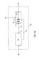
- FIG. 16is a schematic view of a typical remote plasma generator
- FIG. 17is a perspective view of the vapor delivery system of the present invention.
- FIG. 18is a schematic drawing of a representative liquid mass flow controller of the present invention.
- FIG. 19is a schematic drawing of a representative liquid delivery system having one vaporizer
- FIG. 20is a schematic drawing of a representative liquid delivery system having two vaporizers
- FIG. 21is a table summarizing Liquid Alignment Configurations of the vapor delivery system.
- the present inventionis directed to a novel liquid delivery system, chemical vapor deposition (CVD) chamber, exhaust system and remote plasma generator which together comprise a unique system especially useful in depositing thin metal-oxide films as well as other films requiring vaporization of low volatility precursor liquids.
- the systemalso provides for an in-situ cleaning process for the removal of metal-oxide films deposited on interior surfaces of a deposition chamber.
- the systemalso has application in the use of fabricating metal-oxide dielectrics useful in making ultra large scale integration (ULSI) DRAM and other advanced feature electronic devices which require the deposition of high dielectric constant materials.
- ULSIultra large scale integration
- devices that can be made with the system of the present inventionare those devices characterized by having one or more layers of insulating, dielectric or electrode material on a suitable substrate such as silicon.
- a suitable substratesuch as silicon.
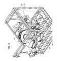
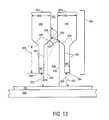
- FIG. 2is a perspective view of the processing system 100 showing the relative positions of the main components of the present invention.
- System 100contains a processing chamber 200 , a heated exhaust system 300 , a remote plasma generator 400 and a vapor delivery system 500 .
- a central substrate transfer chamber 110representative of a cluster tool embodiment of the processing system of the present invention.
- Processing chamber 200is comprised of lid 205 and chamber body 210 and is attached to central transfer chamber 110 .
- Gases supplied via liquid delivery system 500are provided into a processing region 202 (not shown) within chamber 200 via temperature controlled conduits formed within inlet block 272 , mixing block 266 and central block 262 .
- Cartridge style heaters 264are integrally formed into each block and, in conjunction with individual thermocouples and controllers, maintain temperature set points within the conduits. For clarity, individual thermocouples and controllers have been omitted. Not visible in FIG. 2 but an aspect of the present invention is embedded lid heater 235 located integral to lid 205 beneath heater backing plate 234 .
- Chamber 200 processing by-productsare exhausted via heated exhaust system 300 which is coupled to chamber 200 via exhaust port 305 . Also shown are isolation valve 310 , throttle valve 315 , chamber by-pass 320 , cold trap 325 and cold trap isolation valve 330 . For clarity, specific embodiments of vacuum pump 335 and wafer fabrication plant exhaust treatment systems 340 are not shown. In order to provide a clearer representation of the interrelationship between and relative placement of each of the components of heated exhaust system 300 , the jacket type heaters, thermocouples and controllers used to maintain setpoint temperatures in exhaust port 305 , isolation valve 310 , throttle valve 315 , chamber by-pass 320 , and by-pass line 322 have been omitted.
- Activated speciesare generated by remote plasma generator 400 and provided to a processing region within chamber 200 via conduits within activated species inlet block 420 , activated species block 270 and central block 262 .
- Other components of remote plasma generator 400such as magnetron 402 , auto tuner controller 410 , and auto tuner 408 are visible in FIG. 2.
- liquid delivery system 500is liquid flow meter 510 and vaporizer 520 .
- Three-way inlet valve 588allows either precursor 503 or solvent 591 into vapor delivery system 500 .
- Heat exchangers 530 and 582preheat carrier gases and process gases respectively. Heated carrier gases travel via a carrier gas supply line 532 to vaporizer 520 in order to facilitate more complete vaporization within vaporizer 520 as well as carry vaporized liquids to chamber 200 .
- chamber by-pass valve 545allows vapor to be ported either to processing region 202 in chamber 200 via outlet 582 or to exhaust system 300 via outlet 555 which is coupled to heated by-pass line 322 .
- thermocouple and controllerwhich maintain the temperature of chamber by-pass valve 545 and vaporized precursor line 560 as well as the jacket style heater, thermocouple and controller which maintain the temperature of by-pass line 322 have been omitted so as not to obscure the components of liquid delivery system 500 and their relationship to chamber 200 and heated exhaust system 300 .
- the size and dimensions of the various components and the placement of these components in relation to each otherare determined by the size of the substrate on which the processes of the present invention are being performed.
- a preferred embodiment of the inventionwill be described herein with reference to a processing system 100 adapted to process a circular substrate, such as a silicon wafer, having a 200 mm diameter.
- a processing system 100adapted to process a circular substrate, such as a silicon wafer, having a 200 mm diameter.
- FIG. 3is a perspective view of a plurality of processing systems 100 arranged in a cluster tool arrangement around central substrate transfer chamber 110 and supported by common mainframe support structure 105 .
- the Centura® mainframe systemmanufactured by Applied Materials, Inc. of Santa Clara, Calif., is representative of one such cluster tool arrangement.
- This arrangementallows multiple chambers, shown here comprising four processing systems 100 of the present invention, to share a common vacuum transfer 110 .
- One advantage of such an arrangementis that the central substrate transfer also has attached to it a loadlock or loadlocks which hold a plurality of substrates for processing in chambers attached to the central substrate transfer 110 .
- FIG. 3illustrates four identical processing systems 100
- another advantage of the cluster tool arrangementis the ability to place a variety of chamber types onto a single central substrate transfer 110 .
- a substratemay move between chambers arranged around central substrate transfer 110 without exposure to an air or oxygen ambient.
- either one or a plurality of deposition systems 100may be arranged in communication with central substrate transfer 110 with a variety of predetermined chamber types such that a substrate could be loaded into the loadlock attached a central substrate transfer 110 , sequence through the various chambers and as a result of the sequencing form predetermined and desirous films on a substrate processed in this manner.
- deposition system 100in conjunction with other chamber types, would be capable of forming complete portions of an IC. Specifically anticipated is the selection of chamber types, sequencing and liquid delivery configurations which would result in the formation of a representative stack capacitor having polysilicon bottom and top electrodes separated by silicon nitride and titanium nitride barrier layers which are separated by a tantalum oxide dielectric layer. Other layers and structures are also anticipated and are intended to be included within the capabilities of the methods and apparatus described herein. It is also specifically anticipated that a single deposition system 100 would alone have the processing capability of forming complete portions of an IC.
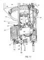
- Chamber 200is shown with protective cover 203 in place.
- Cover 203encloses heated chamber lid 205 and temperature controlled conduit blocks 272 , 266 and 262 .
- Cover 203is maintained at a relatively safe temperature so as to prevent burn injuries from contact with the heated components of lid 205 .
- Remote plasma generator 400is also shown in an alternative embodiment in which the generator is supported from the top of mainframe 105 instead of from below as shown in FIG. 2. So as not to obstruct the view of an alternative embodiment of remote plasma generator 400 , heated exhaust system 300 is not shown.
- Such a support arrangement of remote plasma generator 400provides easier accessibility and maintenance of other components of deposition system 100 as well as contributing to the reduction of the overall footprint of deposition system 100 .
- the embodiment of the plurality of processing systems 100 of FIG. 3further illustrate the compact design features of system 100 of the present invention.
- FIG. 4is a cross sectional view of chamber assembly 200 of processing system 100 of FIG. 2.
- Chamber body 210 and heated chamber lid 205which is hingedly connected to chamber body 210 , together with o-ring 245 form a temperature and pressure controlled environment or processing region 202 which enables deposition processes and other operations to be performed within processing region 202 .
- Chamber body 210 and lid 205are preferably made of a rigid material such as aluminum, various nickel alloys or other materials having good thermal conductivity.
- O-ring 245could be formed from Chemraz, Kalrez, Viton or other suitable sealing material.
- an annular processing region 202is formed which is bounded by showerhead 240 , substrate support 250 and the walls of chamber body 210 .
- Substrate support 250(shown in the raised position for processing) extends through the bottom of chamber body 210 .
- a resistive heaterwhich receives power via resistive heating element electrical connector 257 .
- a thermocouple in thermal contact with substrate support 250senses the temperature of substrate support 250 and is part of a closed loop control circuit which allows precise temperature control of heated substrate support 250 .
- Substrate support 250 and substrate 201are parallel to showerhead 240 .
- Substrate 201is supported by the upper surface of support 250 and is heated by the resistive heaters within substrate support 250 to processing temperatures of, for example, between about 400° C. and 500° C. for Tantalum films formed using the methods and apparatus of the present invention.
- Processing chamber 200is coupled to central transfer chamber 110 via opening 214 .
- a slit valve 215seals processing region 202 from central transfer chamber 110 .
- Substrate support 250may also move vertically into alignment with opening 214 which, when slit valve 215 is open, allows substrates to move between the processing region 202 and central substrate transfer chamber 110 .
- Substrate 201can be a substrate used in the manufacture of semiconductor products such as silicon substrates and gallium arsenide substrates and can be other substrates used for other purposes such as substrates used in the production of flat panel displays.
- Outlet port 260provides fluid communication between components of heated exhaust system 300 and processing region 202 .
- a feature of showerhead 240 of the present inventionis the plurality of apertures 249 , or alternative aperture embodiment 238 , which are not indicated in FIG. 4 so as not to unnecessarily obscure understanding specific details and features of chamber 200 and heated lid 205 .
- Process gas and vaporized precursors and mixtures thereofare provided to central bore through 230 via temperature controlled conduits formed integral to heated feed through assembly 220 .
- Heated feed through assembly 220is comprised of central block 262 , mixed deposition gas feed through block 266 and inlet and mixing block 272 .
- the embodiment represented in chamber 200 of FIG. 4indicates a heated feed through assembly 220 comprising three separate blocks 262 , 266 and 272 , one of ordinary skill will appreciate that the blocks can be combined such as replacing inlet and mixing block 272 and feed through block 266 with a single block without departing from the spirit of the present invention.
- a plurality of cartridge heaters 264are disposed internal to each of the aforementioned blocks and proximate to the conduits 231 , 273 , 278 , 265 , and 276 which maintain a setpoint in each conduit utilizing separate controllers and thermocouples for the heater of a particular conduit. For clarity, the separate thermocouples and controllers have been omitted.
- Lid 205is also provided with a cooling channel 244 which circulates cooling water within that portion of lid 205 in proximity to o-ring 245 .
- Cooling channel 244allows lid 205 to maintain the temperatures preferred for advantageous heating of showerhead 240 while protecting o-ring 245 from the high temperatures which degrade the sealing qualities of o-ring 245 thereby making o-ring 245 more susceptible to attack by the reactive species generated and supplied to processing region 202 by remote plasma generator 400 .
- FIG. 4Another feature of processing chamber 200 of the present invention also shown in FIG. 4 is embedded resistive heater 235 within lid 205 .
- This feature of chamber assembly 200provides elevated temperatures in lid 205 in proximity to central bore through 230 and the area between the lower surface of the lid 205 and showerhead upper surface 263 .
- the region between lid 205 and showerhead upper surface 263is referred to as the “gas box”.
- Formed within the top surface of lid 205is an annular groove shaped according to the size and shape of imbedded heater 235 in order to increase surface contact and heat transfer between resistive heater 235 and lid 205 . Without heater 235 , cooling channel 244 could continuously remove heat from lid 205 .
- cooling channel 244also affects the temperature of portions of lid 205 in contact with precursor vapor, such as the area surrounding central bore through 230 and the gas box. While cooler lid 205 temperatures improve conditions for o-ring 245 , cooler lid 205 temperatures could result in undesired condensation of precursor vapor.
- resistive heater 235is positioned to heat those portions of lid 205 in contact with the vaporized precursor flow such as the gas box and the area surrounding central bore through 230 . As shown in FIG. 4, for example, heater 235 is located between cooling channel 244 and central bore through 230 while also positioned to provide heating to the lid surface adjacent to blocker plate 237 .
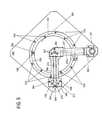
- FIG. 5is a top view of lid 205 , the relationship of embedded heater 235 to other components mounted on lid 205 can be better appreciated.
- Embedded heater 235is indicated in phantom and is located beneath backing plate 234 .
- Backing plate 234 and fasteners 243help increase the surface area contact between embedded heater 235 and lid 205 thereby improving the efficiency of heat transfer between heater 235 and lid 205 .
- Lid 205also has an embedded thermocouple 204 for monitoring the temperature within lid 205 in proximity to heater 235 .
- Thermocouple 204is part of a feedback control circuit which monitors and controls the power supplied to heater 235 to obtain a set point temperature within lid 205 .
- Precise temperature controlis desired in lid 205 , as in all components in contact with vaporized precursor, in order to provide conditions which neither condense nor decompose low vapor pressure precursors such as TAT-DMAE and TAETO.
- heater 235could have a 650 W output rating and is commercially available from a variety of commercial sources such as Watlow, Inc. of Richmond, Ill. Temperature setpoints between about 80° C. and 180° C. are readily obtained in lid 205 utilizing a heater 235 rated at about 650 Watts. It will be appreciate that various heater ratings, set-points and configurations could be utilized to obtain a wide range of temperature set-points depending upon the decomposition and condensation temperatures and other characteristics of the precursor material used.
- imbedded heater 235is represented by a single, continuous, circular element, one of ordinary skill will appreciate that alternative embodiments wherein a plurality of continuous or discontinuous embedded heaters 235 are arranged within lid 205 to provide additional heat or greater temperature control within lid 205 are within the scope of the present invention.
- heated lid 205provides support for showerhead 240 and blocker plate 237 .
- showerhead 240is attached to lid 205 via a plurality of evenly spaced fasteners 242 and blocker plate 237 is attached to lid 205 by a plurality of evenly spaced fasteners 217 .
- Fasteners 217 and 242are formed from a rigid material such as aluminum, varieties of nickel alloys and other materials having good thermal conductivity. Fasteners 242 and 217 provide clamping force which increases the contact area between heated lid 205 and the and the gas distribution components 237 and 240 .
- Fasteners 242 and 217have been advantageously placed to provide clamping force to increase contact between heated lid 205 and showerhead 240 in the case of fasteners 242 and heated lid 205 and blocker plate 237 in the case of fasteners 217 .
- Increased contact areaproduces greater heat transfer between heated lid 205 and blocker plate 237 and showerhead 240 .
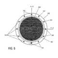
- FIGS. 6 and 8illustrate a plan views of showerhead lower surface 284 as viewed from a substrate 201 positioned on substrate support 250 . Viewed from substrate 20 land looking towards lid 205 as in FIGS. 6 and 8 evenly spaced fasteners 242 are visible on the periphery of showerhead lower surface 284 .
- showerhead 240also comprises a plurality of apertures 249 (FIG. 6 ) and 238 (FIG. 8 ) which allow gases and activated species to enter processing region 202 .
- FIG. 7is a sectional view of an embodiment of a plurality of representative apertures 249 which is indicated as view L-L on FIG. 5.
- Aperture 249includes an upper region 291 , a conical region 290 and a lower region 248 .
- a plurality of apertures 249are distributed across showerhead 240 thereby allowing gases to flow from blocker plate 237 through aperture 249 to substrate 201 .
- Gas from blocker plate 237flows onto showerhead upper surface 263 and into inlets 291 of apertures 249 .
- Inlet 291is axially symmetric to aperture centerline 267 and could be cylindrically shaped with a diameter 247 of 0.028 inches.
- Inlet 291is bounded by showerhead upper surface 263 and inlet parallel walls 269 .
- Gasflows out of inlet 291 and into lower conical region 290 which is defined by divergent walls 255 which are axially symmetric to aperture centerline 267 .
- lower conic region 290has an upstream diameter 256 measured between walls 255 which is smaller than a downstream lower conic region diameter 258 .
- Extending divergent walls 255 to intersect at vertex 259 , as indicated by dashed lines 296angle ⁇ is formed. Angle ⁇ is axially symmetric to aperture centerline 267 such that vertex 259 is on and bisected by aperture centerline 267 . Angle ⁇ is measured between divergent walls 255 and vertex 259 .
- the angled surfaces of divergent walls 255are presented to substrate 201 .
- outlet 248which has parallel walls 281 , a diameter 288 and is axially symmetric about centerline 267 .
- Parallel walls 281have a length 283 measured between the intersection of divergent walls 255 and parallel walls 281 and showerhead lower surface 284 . Gas flowing out of outlet 248 flows towards substrate 201 within processing region 202 .
- inlet diameter 247is less than outlet diameter 288 or inlet diameter 247 could be about one-third of outlet diameter 288 such as when a representative aperture 249 has an inlet diameter 247 of 0.028 inches and an outlet diameter 288 of 0.086 inches.
- aperture 249Another aspect of aperture 249 is the ratio between length 283 of outlet parallel walls 281 and outlet diameter 288 where length 283 is greater than diameter 288 or where length 283 is about 2.5 times outlet diameter 288 .
- a representative aperture 249could have an outlet diameter 288 of about 0.086 inches and a length 283 of about 0.221 inches.
- Another aspect of aperture 249is that length 283 of parallel walls 281 is greater than the length of divergent walls 255 or where parallel walls 281 are about 5.5 times as long as divergent walls 255 .
- the length 283is about 0.221 inches and the length of divergent walls 255 is about 0.041 inches which results in a ratio of the length 283 of parallel walls 281 to the length of divergent walls 255 of about 5.39.
- representative dimensions for each of a plurality of apertures 249 in a representative showerhead 240 fabricated from aluminum having a thickness of about 0.5 inchesare: an inlet diameter 247 of about 0.028 inches; with inlet parallel walls 269 of about 0.25 inches; an outlet diameter 288 of about 0.086 inches with outlet parallel walls length 283 of about 0.221 inches.
- FIG. 9is a sectional view of an embodiment of a single alternative aperture 238 indicated by view D-D on FIG. 8.
- a plurality of apertures 238are distributed across showerhead 240 thereby allowing gases to flow from blocker plate 237 through aperture 238 to substrate 201 .
- Aperture 238includes an upper region 291 , an upper conical region 289 , a central region 246 , a lower conical region 290 and a lower region 248 . Gas from blocker plate 237 flows onto showerhead upper surface 263 and into inlet 291 .
- Inlet 291is axially symmetric to aperture centerline 267 and could be cylindrically shaped with a diameter 247 of 0.110 inches. Inlet 291 is bounded by showerhead upper surface 263 and inlet parallel walls 269 . Gas flows through inlet 291 into upper conic region 289 which is bounded by converging walls 251 . Upper conic region 289 is axially symmetric to aperture centerline 267 and has a decreasing downstream diameter such that an upper conic region upstream diameter 252 is greater than an upper conic region downstream diameter 253 . Converging walls 251 , if extended to an intersection point as indicated by dashed lines 295 , would intersect at vertex 254 forming an angle a.
- Angle ais axially symmetric to aperture centerline 267 such that vertex 254 is on aperture centerline 267 and angle a is bisected by aperture centerline 267 .
- Angle ⁇measured between convergent walls 251 and vertex 254 , is between about 25° and about 45°.
- central conduit 246which is axially symmetric to aperture centerline 267 .
- Central conduit 246could be cylindrically shaped with a diameter 287 of about 0.028 inches.
- Central conduit 246acts as a coupling conduit joining the upper conic region 289 and the lower conic region 290 thus allowing gas flow from inlet 291 to outlet 248 .
- lower conic region 290has an upstream diameter 256 between walls 255 which is smaller than a downstream lower conic region diameter 258 .
- Angle ⁇is axially symmetric to aperture centerline 267 such that vertex 259 is on and bisected by aperture centerline 267 .
- Angle ⁇is measured between divergent walls 255 and vertex 259 .
- the angled surfaces within showerhead 240 formed by divergent walls 255are presented to substrate 201 .
- Outlet 248Gas flows from lower conic region 290 into outlet 248 which is axially symmetric about centerline 267 .
- Outlet 248could be cylindrically shaped having parallel walls 281 and a diameter 288 .
- Parallel walls 281have a length 283 measured between the intersection of divergent walls 255 and parallel walls 281 and showerhead lower surface 284 .
- Gas flowing out of outlet 248flows towards substrate 201 within processing region 202 .
- aperture 238The geometry and other specific aspects of aperture 238 are more clearly understood by describing the ratios between various aperture components.
- One aspect of aperture 238is that inlet diameter 247 is less than outlet diameter 288 or inlet diameter 247 is about one-half of outlet diameter 288 .
- a representative aperture 238could have an inlet diameter 247 of 0.110 inches and an outlet diameter 288 of 0.213 inches.
- Another aspect of aperture 238is the ratio between the inlet 247 and outlet 288 diameters and the central region diameter 287 where central region diameter 287 is less than both inlet diameter 247 and outlet diameter 288 .
- Central region diameter 287is about 0.25 of inlet diameter 247 and about 0.13 of outlet diameter 288 .
- a representative aperture 238could have an inlet diameter 247 of 0.110 inches, an outlet diameter 288 of 0.213 inches and a central region diameter of about 0.028 inches.
- aperture 238Another aspect of aperture 238 is the ratio between length 283 of outlet parallel walls 281 and outlet diameter 288 where length 283 is less than diameter 288 .
- length 283is about three quarters or about 0.7633 of diameter 288 , as in an outlet 248 having a length 283 of 0.1569 inches and a diameter 288 of 0.213 inches.
- Another aspect of aperture 238is that the length 283 of parallel walls 281 is greater than the length of divergent walls 255 or where parallel walls 281 are about 1.5 times as long as divergent walls 255 .
- the length 283is about 0.1569 inches and the length of divergent walls 255 is about 0.1021 inches which results in a ratio of the length 283 of parallel walls 281 to the length of divergent walls 255 of about 1.53.
- dimensions for each of a plurality of representative apertures 238 in an aluminum showerhead 240 having a thickness of about 0.4 inchesare: an inlet diameter 247 of about 0.110 inches; a central cylindrical region diameter 287 of about 0.028 inches with parallel walls 286 of about 0.080 inches; and an outlet diameter 288 of about 0.213 inches with outlet parallel walls 281 length 283 of about 0.1569 inches and divergent walls 255 of about 0.1021 inches.
- inlet 291 , central conduit 246 and outlet 248 of an aperture 238 as well as the inlet 291 and outlet 248 of an apparatus 249may also have various other shapes such as heptagonal, octagonal or other higher order polygons without departing from the scope of the present invention. It is to be appreciated that the above cited specific details with respect to aperture 238 and 249 are only representative embodiments of the unique aperture geometry of the present invention.
- one key factor for controlling deposition rateis the temperature of substrate 201 .
- temperature variations which influence substrate 201should be minimized to assist in obtaining more uniform deposition rates.
- One source of temperature variationoccurs when radiant energy from substrate 201 and heated substrate support 250 reflects off showerhead 240 back to substrate 201 . This redirected reflected energy is uncontrolled and asymmetric resulting in temperature variations within a single substrate 201 and in consecutively processed substrates 201 .
- showerhead lower surface 284 and divergent walls 255 of apertures 249 and 238are reflected surfaces for radiant energy from substrate 201 and heated substrate support 250 .
- Advantageously selecting the aperture geometry presented to substrate 201is one method of increasing the emissivity of showerhead 240 .
- FIGS. 6 and 8Two features of apertures 238 and 249 of the present invention which increase the emissivity of showerhead 240 are spacing 261 between apertures and the advantageous geometry of aperture outlets 248 .
- the advantageous geometry of outlet 248is discussed in detail below with respect to FIG. 13.
- FIGS. 6 and 8a plurality of apertures 249 , shown in FIG. 6, and apertures 238 , shown in FIG. 8, are evenly distributed across showerhead 240 resulting in a pattern of outlets 248 in showerhead lower surface 284 .
- FIG. 10, which is an enlarged view E indicated on FIG. 8,represents the spatial relationship between adjacent outlets 248 regardless of aperture type. Outlets 248 are spaced across showerhead lower surface 284 such that the flat, reflective space between adjacent outlets 248 is minimized.
- the spacing between outlets 248 , spacing 261which represents the width of the flat reflective space between outlets 248 should be as small as possible.
- Another method of spacing outlets 248 across showerhead 240 lower surface 284is to separate adjacent aperture centerlines 267 by some constant distance 285 .
- Constant spacing distance 285is selected based on outlet diameter 248 and desired spacing 261 . For example, an aperture 238 having an outlet diameter 248 of 0.213 inches and a desired spacing 261 of 0.005 inches would have a centerline spacing 285 of 0.218 inches. In another example, an aperture 238 having an outlet diameter 248 of 0.086 inches and a desired spacing 261 of 0.012 inches would have a centerline spacing 285 of 0.098 inches.
- spacing 261decreases for a given size showerhead 240 . This not only reduces the reflective surface between outlets 248 but also increases the amount of angled reflective surface created by divergent walls 255 of each aperture.
- the distribution of apertures 249 and 238can be viewed as replacing the flat, highly reflective surface between outlets 248 of lower showerhead surface 284 with divergent walls 255 .
- Distributing apertures 249 and 238 by minimizing outlet spacing 261increases the number and density of apertures 249 and 238 which correspondingly increases the number and density of divergent walls 255 presented to substrate 201 . As the amount of divergent wall surface area increases, the probability that incident radiation onto showerhead 240 will be reflected and absorbed into showerhead 240 also increases.
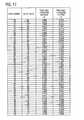
- FIG. 11is a table listing representative aperture 238 locations using a coordinate system having X and Y axes similar to the system shown in FIG. 7 with an origin in the center of showerhead 240 .
- FIG. 11indicates ordinate and abscissa values for a first aperture 238 in a row of apertures 238 which form a representative distribution of apertures 238 having a minimized flat surface 261 between each aperture 238 .
- FIG. 11as a guide for the placement of each aperture 238 results in the distribution of about 1574 apertures 238 across showerhead 240 .
- FIG. 12is a table listing representative aperture 249 locations using a coordinate system having X and Y axes similar to the system shown in FIG. 6 with an origin in the center of showerhead 240 used for processing 200 mm diameter substrates 201 .
- FIG. 12indicates ordinate and abscissa values for a first aperture 249 in a row of apertures 249 which form a representative distribution of apertures 249 having a minimized flat surface 261 between each aperture 249 .
- FIG. 12as a guide for the placement of each aperture 249 results in the distribution of about 6165 apertures 249 across showerhead 240 .
- This distribution patternis similar to the pattern of outlets 248 illustrated in FIG. 6.
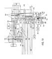
- FIG. 13is a sectional view of an aperture according to aperture 249
- the aspects of the present invention which followalso apply to aperture embodiment 238 as well as to other specific aperture embodiments made according to the present invention.
- the specific geometric arrangement between divergent walls 255 , angle ⁇ , parallel walls 281 and outlet diameter 288is selected in order to increase the emissivity of showerhead 240 . More specifically, by advantageously selecting an angle ⁇ , for example, outlet diameter 288 and length of parallel walls 281 can be selected such that radiation reflected off divergent walls 255 is absorbed into showerhead 240 . The reflected radiation could then, for example, be absorbed into showerhead 240 through single reflections or multiple reflections with walls 281 or other aperture surfaces within showerhead 240 .
- Radiation 222represents that radiation normal to showerhead lower surface 284 .
- the resultis normal reflected radiation 223 . It will be appreciated therefore, that as aperture spacing 261 decreases, more normal radiation 222 will be incident onto divergent walls 255 and the highly absorptive geometry of apertures 238 or apertures 249 .
- divergent walls 255 and outlet walls 281are utilized to facilitate absorption of reflected radiation into showerhead 240 .
- Divergent walls 255 and the angle ⁇ between themprovide a reflective surface to representative incident radiation 206 and 208 .
- incident radiation 208intersects divergent wall 255 .
- a portion of radiation 208will be absorbed by wall 255 and a portion will be reflected as radiation 209 .
- reflected radiation 209intersects wall 269 .
- a portion of radiation 209is absorbed in the first intersection and a portion is reflected. This process of absorption and reflection continues as reflected radiation 209 is reflected and absorbed by walls 269 .
- incident radiation 206intersects divergent wall 255 and a portion of radiation 206 is absorbed by wall 255 .
- a portion of radiation 206is reflected by wall 255 forming reflected radiation 207 .
- reflected radiation 207crosses lower region 248 and intersects an adjacent divergent wall 255 .
- a portion of radiation 207is absorbed by wall 255 and a portion is reflected.
- FIG. 13illustrates an aperture configuration where radiation 206 —i.e. radiation reflected into lower region 248 —is absorbed into walls 281 .
- angle ⁇ , length 283 and diameter 288could be selected such that radiation reflected into the lower region 248 would have multiple refection and absorption reactions with walls 281 and 255 .
- apertures according to the present inventionwill first reflect radiation using divergent walls 255 then absorb radiation via parallel walls 281 thereby reducing reflective radiation produced by showerhead 240 .
- walls 281are generally between about 1.5 and 5.5 times the length of divergent walls 255 for a given angle ⁇ .
- divergent walls 255are about 0.04,1 inches while walls 281 are about 0.221 inches.
- divergent walls 255are about 0.1021 inches while walls 281 are about 0.1569 inches.
- the emissivity ( ⁇ ) of the surface of showerhead 240is intended to be as high as possible in order to approximate the emissivity of a black body.
- An object of the present inventionis to provide showerhead 240 emissivity in the range of about 0.6 to about 0.9.
- surface finishing techniquessuch as anodization, oxidation, ceramic coating or bead blasting may be employed to obtain the desired emissivity.
- Film accumulation on showerhead 240occurs during sequential deposition processes within processing region 240 . A showerhead with film deposits absorbs more incident radiation than a showerhead without those accumulations.
- the resulting absorption variation and temperature difference film accumulation causesis a source of thickness uniformity variation between consecutively processed wafers.
- the resulting accumulation of filmcauses an average emissivity change ( ⁇ ch ) of 0.05 in showerhead 240 .
- ⁇ chaverage emissivity change
- a showerhead having a unpolished metal surfacemay have an emissivity ( ⁇ um ) of about 0.4.
- ⁇ umcould have been increased by ⁇ ch or 0.05 to 0.45 representing a 12.5% change in emissivity.
- ⁇ omoxidized metals with an emissivity
- highly oxidized metals ( ⁇ 0.7) or even anodized surfaces ( ⁇ 0.9)are employed does the impact of representative emissivity change ⁇ ch produce emissivity variation below 10%.
- An object of the present inventionis to increase the absorptive characteristics or emissivity of showerhead 240 such that the emissivity variation induced by film accumulation is reduced or, in other words, the emissivity of showerhead 240 is sufficiently high that it could be said to be invariant.
- Another object of the present inventionis to reduce the temperature variations from one substrate 201 to another in a continuously running reactor as in, for example, reactors utilized in reaction rate limited processes such as the deposition of tantalum pentaoxide.
- Either of the emissivity increasing methods described abovei.e., modification of showerhead surface or selecting highly absorptive aperture geometry
- reflective surfaces on lower showerhead surface 284have been minimized by adjusting the spacing 261 between outlets 248 . Minimizing the spacing 261 between outlets 248 effectively substitutes the divergent walls 255 of apertures 238 and 249 in the place of flat, highly reflective surfaces.
- the divergent walls 255 and shape of lower conic region 290 in conjunction with parallel walls 281 of each of the plurality of apertures 238 , or alternatively 249result in reflective radiation patterns which will likely be absorbed by showerhead 240 instead of reflected back to substrate 201 .
- the emissivity of the material forming showerhead 240has been modified resulting in a is sufficiently high emissivity such that emissivity varying events, such as the accumulation of deposits during substrate processing, result in an over all emissivity change of less than 10%.
- the showerhead emissivitycould be said to be invariant since emissivity change as a result of wafer processing operations within processing region 202 is slight or less than 10% of total emissivity.
- sequentially processed wafersare exposed to a more similar processing environment since the emissivity of a showerhead of the present invention is nearly constant or invariant between consecutive wafers.
- the elevated temperature of showerhead 240which results from increased absorption of radiation provides several advantages to chamber 200 .
- the elevated temperature achieved in showerhead 240can reduce or completely prevent undesirous vapor condensation which may likely occur or occur at a greater rate at lower showerhead temperatures.
- Another advantageis that as the temperature of showerhead 240 increases, the temperature difference between showerhead 240 and substrate 201 decreases. As the temperature difference decreases, the rate of heat transfer between the substrate and the showerhead also decreases. Controlling or minimizing heat losses from substrate 201 is critically important in reaction rate limited processes, such as the formation of Tantalum oxide which is an object of processing system 100 of the present invention.
- the rate of heat loss from substrate 201impacts the deposition temperature which is one influential factor for controlling deposition rate and thickness uniformity of films formed on substrate 201 . Therefore, decreasing the rate of heat transfer from substrate 201 to showerhead 240 reduces a source of deposition rate and thickness variation.
- FIG. 14is a cross section of chamber 200 and schematic portions of vapor delivery system 500 , specific aspects of the temperature controlled conduits feature of chamber 200 of the present invention can more fully appreciated. Also shown is one feature of the vapor delivery system of the present invention illustrating the continuous, independent temperature controlled conduits which couple the outlet of vaporizer 520 with processing region 202 . Given the low vapor pressure of the Tantalum precursor, another feature of the vapor delivery system is the shortened vapor flow path from vaporizer 520 to processing region 202 . By shortening the precursor vapor flow path, pumping losses, friction losses and other fluid dynamic inefficiencies associated with the length of the pumping conduit as well as the inherent difficulties of pumping low vapor pressure gases can be reduced.
- the reduction of the above fluid lossesis beneficial to the effective vaporization and delivery of low vapor pressure precursors according to the present invention.
- the vapor delivery system of the present inventionis able to attain more stable and repeatable vapor flow rates for low vapor pressure precursors.
- heated gas feed through 220Inlet and mixing block 272 , mixed deposition gas feed through block 266 and central mixing block 262 , collectively referred to as heated gas feed through 220 , are formed from rigid materials such as aluminum, varieties of nickel alloys or other materials having good thermal conductivity.
- the various conduits formed within heated gas feed through assembly 220couple the outlets of heated chamber feed through 225 and process gas feed through 227 and lid bore throughs 226 and 228 to central chamber bore through 230 .
- Inlet and mixing block 272attaches to lid 205 forming a sealed, continuous flow path between precursor lid bore-through 226 and precursor inlet conduit 265 and between process gas lid bore-through 228 and process gas inlet conduit 276 .
- o-rings formed of Chemraz ® or Kalrez ®are used at lid bore-through outlets 226 and 228 to provide a seal at the mating surfaces between lid 205 and inlet and mixing block 272 .
- Mixing manifold 278merges the process gas and precursor vapor flows into a single gas flow and begins the process of mixing precursor and process gas or gases into a homogeneous mixture for delivery into processing region 202 .
- the length of conduit from the point within mixing manifold 278 where the precursor vapor stream and the process gas stream mixis sufficiently long such that the resulting mixed gas stream is homogeneously mixed upon arrival in processing region 202 .
- specific lengths to achieve homogeneous mixingwill vary depending on a variety of factors such as the diameter of the conduit and gas flow rates and temperatures, a representative length from mixing manifold 278 to processing region 202 would be about 12 inches for a 0.5 inch inner diameter mixed deposition gas conduit 273 , central conduit 231 and bore through 230 of FIG. 14.
- the length of conduit which could also result in homogeneous mixing of precursor vapor and process gases from mixing manifold 278 through mixed deposition gas conduit 273 and central conduit 231 , both having inner diameters of 0.5 inchesis about 10 inches.
- Inlet and mixing block 272attaches to mixed deposition gas feed-through block 266 such that the outlet of mixing manifold 278 is coupled to mixed deposition gas conduit 273 formed within mixed deposition feed-through block 266 .
- the mating surface surrounding the conduit outlet of conduit 278 and the inlet of mixed deposition gas conduit 273is similarly sealed with an o-ring formed of Kalrez ® or Chemraz®.
- Mixed deposition gas feed-through block 266attaches to mixing block 262 and similarly forms an o-ring sealed conduit between mixed deposition gas conduit 273 and central gas feed-through conduit 231 .
- Mixing block 262is attached to heated lid 205 forming an o-ring sealed conduit between central gas feed-through conduit 231 and central lid bore-through 230 .
- inlet mixing block 272 and mixed deposition gas feed through block 266are described and discussed as separate pieces. However, one of ordinary skill in the art will appreciate that a single workpiece could be utilized having the described dimensions and characteristics of both inlet mixing block 272 and mixed gas feed through 266 without departing from the scope of the present invention.
- each of the conduits formed internal to heated manifold 220( 265 , 276 , 278 , 273 and 231 ) are controlled by a plurality of independent heaters 264 , thermocouple 274 and controller 277 units.
- One unitcontrols the temperature of conduits 265 , 276 and 278 within inlet and mixing block 272 ; another controls the temperature of conduit 273 within feed through block 266 ; and another controls the temperature of conduit 231 within central block 262 .
- a plurality of cartridge or fire-rod type heaters 264are advantageously arranged integral to the given block in proximity to the conduit or conduits within a given block.
- heatersprovide the most efficient heating of the particular conduit or conduits within a given block as the heaters can be located based upon the size, shape, composition and thermal conductivity of the particular block as well as the particular geometry of the conduits.
- cartridge heaters 264are about 0.25 inches in diameter, cylindrical in shape, have various lengths, output power capacities and are available commercially from Watlow Inc. of Richmond, 111 . under the brand name “Firerod”.
- the set-point temperatureis maintained within a given conduit by inputting a desired temperature set-point into the controller 277 for the particular conduit.
- Controller 277could be a PID type controller similar to Model 965 which is also commercially available from Watlow, Inc.
- Thermocouples 274are embedded within gas feed through assembly 220 in proximity to each conduit such that the temperature registered by each thermocouple 274 is approximately the same as the temperature within the gas conduit by which the thermocouple is installed.
- the position of thermocouple 274 relative to a given gas conduitvaries depending upon a number of factors such as the thermal conductivity of the material used to fabricate the given block and the type of thermocouple 274 used.
- thermocouple 274The signal from thermocouple 274 is sent to controller 277 which compares the temperature from thermocouple 274 to the input temperature set-point. Based on the result of comparing the temperature from thermocouple 274 to the input temperature set-point, controller 277 will either increase, decrease or maintain power supplied to cartridge heaters 264 .
- controller 277One advantage of utilizing a plurality of independent thermocouples 274 is that the specific conditions of a given conduit block are taken into account depending upon its location relative to other heat sources such as heated lid 205 , heat loses and geometry.
- inlet and mixing feed through block 272is in direct contact with heated lid 205 and, unless the temperatures between them exactly match, will either gain energy from or lose energy to lid 205 .
- the effect of heat transfer between lid 205 and mixing feed through block 272 on the temperature of conduits 265 , 276 and 278 within block 272will be reflected in the temperature detected by a thermocouple 274 located within block 272 .
- the controller 277 associated with block 272can increase or decrease the power output of heaters 264 embedded within block 272 in proximity to conduits 265 , 276 and 278 to compensate for heat transfer between block 272 and lid 205 .
- thermocouple, heater, controller unit associated with block 262energy transfer between mixing block 262 and lid 205 is compensated for by the thermocouple, heater, controller unit associated with block 262 .
- heat losses of mixed deposition gas feed through block 266which are different from heat transfer of blocks 272 and 262 since it has a higher potential for heat loss because it is not in direct contact with heated lid 205 and has a larger surface area exposed to the ambient conditions (about 70 degrees Fahrenheit) within the wafer fabrication facility when protective cover 203 is removed.
- temperatures surrounding manifold 220are increased to about 70 to 80 degrees Celsius.
- the heater, thermocouple, controller unit dedicated to mixed deposition gas feed-through block 266is utilized to compensate for the particular heat transfer characteristics of that block.
- an aspect of the present inventionis a method to provide a predetermined temperature set-point within a conduit by the selection, placement and use of a controller, heater and thermocouple control unit which utilizes the method and apparatus described above.
- Another feature of the multiple, independent cartridge heater, thermocouple and controller units of the present inventionis that a uniform conduit temperature throughout heated gas manifold 220 can be achieved. Because of their independence, each controller is able to efficiently maintain set points irrespective of conditions in surrounding blocks while taking into account the specific heat losses and conditions surrounding each block, the specific outer shapes of each block and the geometry of the conduits formed within each block.
- the temperature set point of each conduitcould be set and maintained to induce a negative temperature gradient where the temperature of block 262 is less than block 266 which is less than the temperature of block 272 .
- a positive temperature gradientcould be induced where the temperature in block 272 is less than the temperature in block 266 which is also less than the temperature of block 262 .
- mixed deposition and feed-through block 266is an aluminum rectangle with the following dimensions: about 5 inches long, about 1.5 inches wide and about 0.75 inches high.
- a representative cartridge heater 264could be cylindrically shaped, 0.25 inches in diameter, 5.5 inches long with a power output capacity of 500 Watts.
- a single cartridge heater 264 or a plurality of heaters 264 of a selected power output capacity of about 500 Wattscould be employed within mixed deposition feed through block 266 such that the temperature within mixed deposition gas conduit 273 remains above the vaporization temperature and below the decomposition temperature of the carrier gas/precursor vapor/process gas mixture flowing within conduit 273 .
- a thermocouple 274could be placed between about 0.125 inches to 0.5 inches away from mixed deposition gas conduit 273 .
- conduit 273temperatures between about 130° C. and 160° C. would prevent both condensation and decomposition of the tantalum/oxygen/nitrogen mixture.
- a typical set-point temperaturecould be about 150° C. or between about 130° C. and 160° C.
- Representative set-points for an embodiment of the present invention employing TAETOcould be about 170° C. or between about 150° C. and 180° C.
- a further aspect of the temperature controlled conduits of chamber 200 of the present inventionprovides temperature controlled delivery of vaporized precursor from vaporizer 520 to lid bore through 230 .
- Vaporized precursorexits vaporizer 520 via vaporizer outlet 540 and enters vaporizer outlet line 542 which is coupled to precursor inlet 544 of chamber by-pass valve 545 .
- precursor vaporexits three way valve 545 via chamber outlet 550 flowing then to precursor chamber supply line 560 which is coupled to precursor feed through 225 .
- a jacket type temperature controlled conduit 292is created between the outlet of vaporizer 520 and the inlet to precursor feed through 225 and encompasses conduits 542 and 560 and three way valve 545 .
- a jacket type control unitcomprises a jacket or wrap style heater 275 , a controller 277 and a thermocouple 274 is utilized to maintain a temperature set-point in the above components 542 , 560 and 545 .
- precursor vaporflows through lid bore through 226 into precursor inlet conduit 265 of inlet and mixing block 272 .
- precursor inlet 265the precursor vapor flows into mixing manifold 278 where it mixes with process and ballast gases supplied via process inlet conduit 276 .
- the temperature of precursor vapor within conduit 225is maintained by the temperature controlled chamber feed through 219 which includes a plurality of cartridge type heaters 264 , a thermocouple 274 and a controller 277 .
- Another feature of temperature controlled precursor feed through 219is thermal choke or air gap 212 which insulates thermal influences of chamber body 210 from the components of temperature controlled precursor feed through 219 .
- Process gas heat exchanger 582provides temperature control to process gas and ballast gases for use in chamber 200 .
- Process gas heat exchanger 582is located proximate to chamber body 210 and, more specifically, to process gas chamber feed through 227 such that the gas temperature exiting heat exchanger 582 is approximately the same as the gas temperature entering feed through 227 .
- temperature controlled process and ballast gasespass through lid bore through 228 and enter process gas inlet 276 of inlet and mixing block 272 .
- process gas heat exchanger 582to heat process and ballast gases above the temperature of the vaporized precursor gas stream.
- the temperature set-point of process gas heat exchangercould be about 5-10° C. above the temperature set-point of vaporizer 520 .
- the temperature of process gas and ballast gascan be controlled to remain below a set-point where, upon mixing with the precursor vapor stream, decomposition of the precursor occurs.
- a set-pointcould be utilized which results in process gas temperatures at least as high as the merging precursor gas stream.
- thermocouple, controller, heater setswhich are part of processing system 200 and vapor delivery system 500 , a series of temperature controlled conduits is provided which can deliver vaporized low vapor pressure precursors from the outlet of vaporizer 520 to processing region 202 .
- temperature controlled conduits based on heater typeare described—cartridge heater temperature controlled conduits 293 and jacket or wrap style heater type temperature controlled conduits 275 —their description is not intended to be limiting as one of ordinary skill in the art will appreciate that a variety of heater types, thermocouples and controllers could be utilized without departing from the scope of the present invention.
- each temperature controlled conduitcould be set to maintain a set-point 2-3° C. hotter than the previous conduit so that a slightly positive thermal gradient is maintained between the vaporizer 520 and outlet of central conduit 231 into processing region 202 or, more generally, an overall ⁇ T could be maintained between the vaporizer outlet temperature and the temperature in central conduit 231 or a ⁇ T of about 20-25° C.
- thermally controlled conduits of processing chamber 200 and vapor delivery system 500 of the present inventionis that the conduits used downstream of vaporizer 520 in the precursor flow path, as shown in FIG. 14 between vaporizer 520 and central lid bore through 205 , have progressively larger diameters which result in increasing cross-sectional flow areas resulting in an expanded gas flow volume within these conduits.
- the volume expansion and corresponding pressure drop within the precursor delivery conduitsfurther help maintain conduit conditions which neither condense nor decompose the vaporized precursor.
- Another aspect of the independent temperature controlled conduits of chamber 200is that temperature changes within a specific conduit associated with the volume expansion can be compensated for by the independent heater, controller and thermocouple of that particular conduit. For example, representative inner diameters for the chamber illustrated in FIG.
- Another aspect of the present inventionis that the cross sectional area of downstream of the intersection of the precursor gas flow and the process gas flow is larger than the sum of the merging gas flows. This relationship ensures that the downstream volume is larger thereby providing the increasing flow volume/decreasing precursor pressure feature discussed above.
- the diameter of mixed deposition precursor conduit 273is also greater than either precursor inlet 265 or process gas inlet 276 .
- the increased volume and correspondingly decreased pressure achieved by advantageously selecting the diameter of conduits downstream of vaporizer 520 such as 542 , 560 , 225 , 226 , 265 , 278 , 273 and 231 in conjunction with the temperature control provided by the thermocouple, heater and controller sets described aboveprovide a controlled temperature and pressure regime between vaporizer 520 and processing region 202 such that very low vapor pressure precursors, such as and including Tantalum precursors like TAETO, TAT-DMAE or other similarly low vapor pressure precursors, dopants or other processing materials may be delivered to processing area 202 without undesired condensation or decomposition.
- very low vapor pressure precursorssuch as and including Tantalum precursors like TAETO, TAT-DMAE or other similarly low vapor pressure precursors, dopants or other processing materials may be delivered to processing area 202 without undesired condensation or decomposition.
- remote plasma apparatus 400shown FIG. 15 in relation to central substrate transfer chamber 110 and chamber 200 and components of heated exhaust system 300 .
- Remote plasma apparatus 400creates a plasma outside of or remote to processing region 202 for cleaning, deposition, annealing or other processes within processing region 202 .
- One advantage of a remote plasma generator 400is that the generated plasma or activated species created by remote plasma generator 400 may be used for cleaning or process applications within the processing region without subjecting internal chamber components such as substrate support 250 or shower head 240 to plasma attack which usually results when conventional RF energy is applied within process region 202 to create a plasma.
- FIG. 15Several components of remote plasma apparatus 400 are visible in FIG. 15 such as magnetron 402 , auto tuner controller 410 , isolator 404 , auto tuner 408 , adapter tube 418 and adapter tube heat insulation disc 424 .
- Magnetron assembly 402houses the magnetron tube, which produces the microwave energy.
- the magnetron tubeconsists of a hot filament cylindrical cathode surrounded by an anode with a vane array. This anode/cathode assembly produces a strong magnetic field when it is supplied with DC power from a power supply. Electrons coming into contact with this magnetic field follow a circular path as they travel between the anode and the cathode. This circular motion induces voltage resonance, or microwaves, between the anode vanes.
- An antennachannels the microwaves from magnetron 402 to isolator 404 and wave guide 406 .
- Isolator 404absorbs and dissipates reflected power to prevent damage to magnetron 402 .
- Wave guide 406channels microwaves from isolator 404 into auto tuner 408 .
- Auto tuner 408matches the impedance of magnetron 402 and microwave cavity 416 to achieve the maximum degree of reflected power by adjusting the vertical position of three tuning stubs located inside wave guide 406 .
- Auto tuner 408also supplies a feedback signal to the magnetron power supply in order to continuously match the actual forward power to the setpoint.
- Auto tuner controller 410controls the position of the tuning stubs within wave guide 406 to minimize reflected power.
- Auto tuner controller 410also displays the position of the stubs as well as forward and reflected power readings.
- Microwave applicator cavity 416is where gas or gases supplied via gas supply inlet 412 are ionized. Gas supplied via gas supply inlet 412 enters a water cooled quartz or sapphire tube within microwave applicator 416 , is subjected to microwaves and ionizes producing activated species which can then be used in cleaning and processing operations within processing region 202 .
- One such cleaning gasis NF 3 which can be used to supply activated fluorine for cleaning processing region 202 when a substrate 201 is not present in processing region 202 .
- Activated speciescan also be used to anneal or otherwise process semiconductor or other materials present on a substrate 201 positioned within processing region 202 .
- An optical plasma sensor 414detects the existence of plasma within cavity 416 .
- Activated species generated within microwave applicator cavity 416are supplied to activated species chamber feed through 229 via adapter tube 418 .
- Adapter tube 418is insulated from the elevated temperature of chamber body 210 by adapter tube isolation disc 424
- activated species conduit 271From activated species chamber feed through 229 , the activated species pass through lid bore-through 221 and enter activated species inlet block 420 which, together with activated species block 270 , provide an o-ring sealed, air tight conduit i.e., activated species conduit 271 , between lid bore-through 221 and central gas feed-through 231 within central mixing block 262 .
- heated exhaust system 300 of processing system 100can be better appreciated.
- the components of heated exhaust system 300are collectively referred to as a foreline are in communication with a vacuum pump 355 (not shown) and wafer fabrication facility exhaust systems 340 (not shown) to provide for reduced pressure processing operations within processing region 202 . Exhaust from processing and cleaning operations conducted within processing region 202 are exhausted via chamber exhaust port 305 .
- isolation valve 310shuts off chamber assembly 200 from down stream vacuum pump systems.
- isolation valve 310is open and throttle valve 315 opens and closes to regulate pressure within processing region 202 .
- By-pass inlet 320receives precursor vapor/carrier gas mixture from chamber by-pass valve outlet 555 when chamber by-pass valve 545 is positioned to flow precursor vapor/carrier gas mixture to temperature controlled by-pass line 322 .
- Exhaust system components exhaust port 305 , isolation valve 310 , throttle valve 315 and by-pass 320 and by-pass line 322are temperature controlled to prevent unreacted precursor condensation.
- Cold trap 325 and remaining downstream exhaust system componentsare maintained at or below 75 degrees Fahrenheit.
- any unreacted vapor remaining in the exhaust stream from processing region 202 or vapor from chamber by-pass valve 545will remain gaseous in the temperature controlled or heated portion of exhaust system 300 and then condense within cold trap 325 thus preventing damage to the vacuum pumps or accumulation and resulting line blockages within exhaust system piping. Additionally, collection of unreacted vapor within cold trap 325 also minimizes the exposure of maintenance personnel to potentially hazardous chemicals.
- Cold trap 325is equipped with an isolation valve 330 for separating cold trap 325 from vacuum pumping systems to allow for routine maintenance or cleaning.
- thermocouple, controller, heater 275utilized as part of the temperature controlled feature of exhaust system 300 is not shown in FIG. 15.
- FIG. 18which is a representative schematic embodiment of processing system 100 of the present invention, the temperature controlled conduits feature of exhaust system 300 can be better appreciated.
- a jacket style heater, thermocouple and controller 275could be utilized to measure and maintain a set point temperature in exhaust port 305 , isolation valve 310 , throttle valve 315 and chamber bypass line 320 thereby creating a jacket heater controlled conduit 292 in the exhaust components upstream of cold trap 325 .
- thermocouple, controller and heater 275operates on by-pass line 322 between chamber by-pass 545 and exhaust by-pass 320 .
- chamber by-pass line 322becomes a jacket style heater temperature controlled conduit 292 between chamber by-pass 545 and exhaust by-pass 320 .
- Vapor delivery system 500provides a method and an apparatus for supplying controlled, repeatable, vaporization of low vapor pressure precursors for film deposition on a substrate 201 located within processing region 202 .
- One methodprovides for the direct injection of vaporized TAETO and TAT-DMAE.
- One of ordinary skillwill appreciate the specific features detailed below which separately and when combined allow vapor delivery system 500 to vaporize and precisely control the delivery of liquid precursors including those precursors having vapor pressures significantly lower than precursors utilized in prior art vapor delivery systems or, specifically, precursors having vapor pressures below about 10 Torr at1 latm and 100° C. (FIG. 1).
- vapor delivery system 500The various components of vapor delivery system 500 are placed in close proximity to chamber 200 in order to minimize the length of temperature controlled vapor passageways between the outlet of vaporizer 520 and processing region 202 . Even though practice in the semiconductor processing arts is to place vapor systems remotely from processing chambers to either ensure serviceability or reduce the amount of cleanroom space occupied by a processing system, vapor delivery system 500 of the present invention utilizes an innovative compact design which allows all system components—less bulk liquid precursor, carrier gas and process gas supplies—to be located directly adjacent to chamber 200 in close proximity to precursor and process gas chamber feed throughs 225 and 227 .
- a low vapor pressure liquid precursorsuch as TAT-DMAE or TAETO
- TAT-DMAE or TAETOcan be stored in bulk storage container 503 located remotely or on mainframe support 105 in proximity to processing chamber 200 .
- Liquid precursor stored in tank 503is maintained under pressure of an inert gas such as Helium at about 15 to 60 psig.
- the gas pressure within tank 503provides sufficient pressure on the liquid precursor such that liquid precursor flows to other vapor delivery system components thus removing the need for a pump to deliver the liquid precursor.
- the outlet of delivery tank 503is provided with a shut-off valve 507 (not shown) to isolate bulk tank 503 for maintenance or replenishment of the liquid precursor.
- liquid precursor from tank 503is provided to liquid supply line 508 and the precursor inlet 509 of precursor/solvent inlet valve 588 .
- precursor/solvent valve 588When aligned for liquid precursor, precursor/solvent valve 588 provides liquid precursor to precursor/solvent outlet 594 and into precursor/solvent supply line 592 to liquid flow meter inlet 505 .
- Liquid flow meter 510measures precursor flow rate and provides via liquid flow meter outlet 511 liquid precursor to vaporizer supply line 513 and then to vaporizer inlet 515 .
- Vaporizer 520in conjunction with a heated carrier gas (described below) converts the liquid precursor into precursor vapor.
- a carrier gassuch as nitrogen or helium, is supplied into carrier gas heat exchanger inlet 525 at a pressure of about 15 psi.
- Carrier gas heat exchanger 530is a gas to resistive heater type heat exchanger like Model HX-01 commercially available from Lintec.
- Carrier gas heat exchanger 530preheats the carrier gas to a temperature such that the heated carrier gas stream entering vaporizer 520 does not interfere with the efficient vaporization of the precursor liquid undergoing vaporization within vaporizer 520 .
- Heated carrier gasis provided to vaporizer 520 via carrier gas supply line 532 and carrier gas inlet to vaporizer 535 .
- carrier gas heat exchanger 530should heat the carrier gas into a temperature range bounded by, at the lower limit, the condensation temperature of the precursor and, at the upper limit, the decomposition temperature of the precursor.
- a representative vaporization temperatureis about 130° C. and a decomposition temperature is about 190° C.
- a typical carrier gas such as nitrogencould be provided to a vaporizer 520 , which is vaporizing a tantalum precursor such as TAT-DMAE, at about between 200 and 2000 standard cubic centimeters per minute (sccm) and a temperature of about between 130° C. and 160° C. These conditions result in a vaporized precursor flow rate in the range of about 10-50 milligrams per minute.
- Carrier gas temperaturecan also be such that the temperature of the carrier gas entering vaporizer 520 is at least as high if not higher than the vaporization temperature of the precursor being vaporized in vaporizer 520 .
- carrier gas temperatures below vaporization conditions within vaporizer 520could sufficiently cool the vaporized precursor, result in condensation and should therefore be avoided.
- liquid flow controller 528schematically represents the operation of liquid flow meter 510 in conjunction with vaporizer 520 , which are referred to collectively as liquid mass flow controller 528 .
- Liquid precursorenters liquid flow meter 510 which generates measured flow rate signal 512 .
- a typical flow rate signalis measured in milligrams per minute or mg/min.
- a representative flow rate for a TAT-DMAE precursoris 35 mg/min. for a representative Ta 2 O 5 film produced utilizing the method and apparatus of the present invention.
- the now measured precursor flowexits liquid flow meter outlet 511 into vaporizer supply line 513 and then into vaporizer inlet 515 .
- Vaporizer supply line 513is typically 0.125 inch outer diameter stainless steel piping.
- liquid mass flow meter 528Another aspect of liquid mass flow meter 528 is that the length of vaporizer supply line 513 is minimized to attain controllable low vapor pressure precursor output from vaporizer 520 . Minimizing the distance between liquid flow meter 510 and vaporizer 520 adds to the number of vapor delivery system 500 components placed in proximity to processing system 100 as well as increases the density of equipment mounted on mainframe 105 . However, vapor delivery system 500 , along with the remote plasma system 400 and heated exhaust system 300 have been designed to minimize interference between the subsystems of processing system 100 while achieving the compact design desired in cluster tool wafer processing systems.
- Vaporizer inlet 515 to liquid flow meter outlet 511 spacing of about 6 inches or between about 4 inches and 15 inchesleads to more effective metering and controlled vaporization of low vapor pressure precursors such as TAETO, TAT-DMAE or other liquid precursors having a vapor pressure of below about 10 Torr at 100° C. and 1 atm.
- FIG. 522Another feature of a the liquid mass flow controller 528 of the present invention is positive shut-off valve 522 .
- positive shut-off valve 522Located within vaporizer 520 between vaporizer inlet 515 and metering valve 524 , positive shut-off valve 522 provides the capability to cut-off liquid flow before the vaporization point within vaporizer 520 .
- Metering valve 524can provide a shut-off capability when in a ‘closed’ or zero set-point condition.
- positive shut-off valve 522provides added assurance that no liquid will continue to flow through vaporizer 520 when liquid mass flow controller 528 is in a ‘closed’ or zero set-point condition.
- the position of positive shut-off valve 522 relative to metering valve 524is such that there is a minimal volume of liquid which could remain in the line between shut-off valve 522 and metering valve 524 .
- a representative vaporizer 520 suitable for vaporization of low vapor pressure liquidscould position positive shut-off valve 522 about one inch or less from metering valve 524 .
- utilizing a 0.125 inch diameter line between shut-off valve 522 and metering valve 524a minimal liquid volume of about 0.012 cubic inches of precursor is created. By reducing the volume between these components the amount of precursor which could vaporize after positive shut-off valve 522 is closed is minimized.
- positive shut-off valve 522provides redundancy to the shut-off capabilities of metering valve 524 as well as provides a minimal volume of liquid which could still be vaporized even if liquid mass flow controller 528 is in a open or 100% flow set-point condition and positive shut-off valve 522 is closed.
- vaporized precursorflows from vaporizer outlet 540 into vaporizer outlet line 542 into vapor inlet 544 of temperature controlled by-pass valve 545 .
- by-pass valve 545supplies vapor to chamber outlet 550 and then into temperature controlled vaporized precursor supply line 560 .
- a feature of the vapor delivery system 500is the thermocouple, controller, jacket style heater system 275 which maintains a temperature set-point within vaporizer outlet line 542 , chamber by-pass valve 545 and vaporized precursor supply line 560 .
- the internal piping of chamber by-pass valve 545allows vaporized precursor/heated carrier gas mixture to be sent to processing region 202 via outlet to chamber 550 .
- chamber by-pass valve 545could direct the vaporized precursor/heated carrier gas mixture to heated by-pass line 320 of heated exhaust system 300 (described above) via outlet to by-pass 555 .
- One advantage of chamber by-pass valve 545 of the present inventionis that once liquid mass flow controller 528 attains a desired set-point vapor flow rate the vaporized precursor/heated carrier gas mixture can either be directed to the chamber for deposition or to the foreline by-pass inlet 320 for disposal. Independent of operations within processing region 202 , liquid mass flow controller 528 continues to produce a stable, consistent vapor flow rate.
- chamber by-pass valve 545 used in conjunction with liquid mass flow controller 528provides the repeatable, stable vapor flow rates to consecutive substrates 201 within processing region 202 .
- Such repeatable, stable vapor flow ratesare necessary for the deposition of transition metal dielectric materials such as tantalum oxide for use in high capacity ICs such as stacked capacitors.
- Vaporizer outlet line 542 and precursor supply line 560are standard piping which could be made of stainless steel. Vaporized precursor supply line 560 should be as short as possible to minimize the length of travel of vaporized precursor within the system or between about 4 to 6 inches. Precursor supply line 560 is in communication with chamber outlet 550 and precursor chamber heated feed-through 225 . In order to prevent condensation of the vaporized precursor within the vaporized precursor/heated carrier gas mixture, heated precursor supply line 560 and vaporizer outlet line 544 , like all precursor supply conduits downstream of vaporizer 520 , have an inner diameter which is greater than the inner diameter of the liquid supply line into vaporizer 520 .
- the vaporizer liquid supply lineis made of stainless steel with about a 0.125 inch inner diameter while the conduits downstream of vaporizer 520 could have a larger diameter or an outer diameter of about 0.5 inches or an inside diameter of about 0.4 inches. Larger diameter conduits downstream of vaporizer 520 exposes the vaporized precursor/heated carrier gas mixture to an expansion volume and corresponding reduction in pressure which helps maintain the vaporized low vapor pressure precursor within an operational temperature region above the precursor condensation temperature and below its decomposition temperature for the conditions within the vapor supply conduits.
- thermocouple, controller, jacket style heater 275temperatures within vaporized precursor supply line 560 and vaporizer outlet 542 are maintained above the condensation temperature and below the decomposition temperature of the vaporized precursor or between about 100° C. and 190° C.
- Vapor delivery system 500also has a temperature controlled process gas feature.
- Process gas heat exchanger 582which is similar to carrier gas heat exchanger 530 described above receives process gas from process gas supply 580 .
- Suitable process gasesdepend on the desired film deposition. Typically, oxygen (O 2 ) and nitrous oxide (N 2 O) are suitable for oxidation processes and ammonia (NH 4 ) is suitable for nitride processes. Additionally, nitrogen (N 2 ) could be added to the process gas flow as a ballast gas.
- process gas stream used belowrefers to all gas flows out of heat exchanger 582 and is intended to include process gas, ballast gases or other gases described below.
- Process gases and ballast gasescan be preheated by process gas heat exchanger 582 so that the resulting process gas stream is maintained above the temperature of the adjacent vaporized precursor gas stream. Maintaining the process gas stream temperature above about 10°-15° C. above the temperature of the vaporized precursor gas stream assists in the prevention of inadvertent condensation of the precursor vapor when the gas streams intersect and begin to mix within mixing conduit 278 . Similarly, heat exchanger 582 can also ensure process gas stream temperatures are maintained below the decomposition temperature of the precursor gas stream so that inadvertent decomposition of the precursor vapor stream does not occur when the gas streams mix within mixing conduit 278 .
- a temperature controlled gas streamexits process gas heat exchanger 582 via outlet 584 and enters process gas supply line 586 .
- the process gas streamflows through process gas chamber feed-through 227 which in flows into heated process gas inlet conduit 276 .
- Process gas inlet conduit 276flows into and mixes with vaporized precursor flow stream in heated mixing manifold 278 .
- Process gas heat exchanger 582heats the process gas to a sufficient temperature such that when the process gas mixes with the vaporized precursor in mixing conduit 278 the precursor vapor neither decomposes nor condenses.
- vapor delivery system 500Another feature of vapor delivery system 500 is the ability to provide a solvent flush capability to those conduits which come into contact with the vaporized low vapor pressure precursors. Such solvent operations further the operability of the method and apparatus of the present invention to vaporize low vapor pressure liquids such as TAETO and TAT-DMAE.
- a solventsuch as anhydrous isopropyl alcohol, methanol, hexane, ethanol, or other suitable solvent is supplied into precursor/solvent three-way valve 588 via solvent inlet 590 .
- solventis introduced into the vapor delivery system 500 , via 3-way valve 588 and follows the same flow path as a vaporized precursor through the various components of vapor delivery system 500 and, depending upon chamber by-pass valve 545 alignment, to chamber 200 or exhaust system 300 via by-pass line 322 .
- the solventflows through the various conduits which are exposed to liquid precursor such as the conduits of and within liquid mass flow controller 528 , the solvent mixes with precursor liquid and purges the line of residual precursor which then allows exposure of the components to air for maintenance or component change.
- the solvent flush featurecan be utilized to remove precursor vapor from process conduits and components to prevent risk of exposure to potentially hazardous materials during maintenance as well as prevent the undesired reaction of precursor vapor with air, water vapor or other materials.
- FIG. 19schematically represents a system configuration when a single vaporizer and process heat exchanger are utilized to provide process gas/precursor vapor mixtures to temperature controlled conduits 292 and 293 and processing region 202 .
- FIG. 20is similar to FIG. 19 with the addition of a second vaporizer 520 , bulk supply 504 and by-pass valve 570 .
- processing system 100 of the present inventionis further enabled to not only provide, mix, and deposit films from a single precursor (FIG. 19) but also, by modifying the liquid source contained in bulk supply 204 , films containing a second precursor, a dopant or a metal.
- Deposition system 100 as embodied in FIG. 20operates similarly to previous descriptions of processing system 100 with the addition of an additional bulk supply 504 which could be under a pressure head as with bulk supply tank 503 .
- Bulk supply 504is coupled to and supplies processing fluids to a second vaporizer 520 which operates similarly to the first vaporizer 520 as embodied in FIG. 19 and described above.
- the vaporized precursor stream created by the second vaporizer 520is provided to a chamber by-pass valve 570 which can align—via outlet 571 —the vaporized gas stream to chamber 200 via process gas supply line 586 .
- by-pass valve 570can align the vaporized precursor stream to exhaust system 300 via outlet 572 .
- bulk supply 504could contain a wide variety of fluid processing source materials such as dopants, precursor materials, metals, or other materials with a sufficiently high vapor pressure that vaporization may occur without a carrier gas, heated carrier gas or will remain vaporized without temperature controlled conduits described above in relation to the low vapor pressure precursor utilized and described above. Therefore, what is not shown, but an object of the present invention is modification of the second vaporizer 520 and other components of FIG.
- Another object of the vapor delivery system 500 present inventionis the deposition of a variety of films on substrates 201 within process area 202 by advantageously selecting precursors bulk supplies 504 and 503 , process gases, process gases or ballast gases for gas source 580 and by selective positioning of by-pass valves 570 and 545 .
- One advantage of the 2 vaporizer—2 by-pass configuration of FIG. 20is that each vaporizer may be in operation and producing stable, repeatable flow which, by aligning the appropriate by-pass 570 or 545 , could easily be ported to process region 202 or exhaust system 300 .
- FIG. 21provides 10 liquid alignment configurations which refer to the specific positions of chamber by-pass valves 545 and 570 , the contents of bulk sources 503 and 504 , process gas source 580 and the resultant vapor mixture delivered to processing area 202 .
- the Liquid Alignment Configurations listed in FIG. 21can be categorized into three broad mixture groups: tantalum oxide mixtures, dielectric mixtures and electrode mixtures.
- Liquid Alignment Configurations 1-4are directed towards tantalum containing mixtures. Since only a single bulk source 503 and vaporizer 520 is utilized, configuration 1 could be embodied by either FIG. 19 or on FIG. 20 where chamber by-pass valve 570 is aligned to by-pass outlet 572 . Whether FIG. 19 or 20 is used, bulk source 503 contains a tantalum containing precursor such as TAT-DMAE or TAETO which is vaporized and provided to chamber by-pass 545 . Chamber by-pass 545 is aligned to chamber or outlet 550 so the vaporized Tantalum flows through chamber by-pass outlet 550 . through temperature controlled conduits 275 , 219 and 293 into mixing manifold 278 .
- a tantalum containing precursorsuch as TAT-DMAE or TAETO
- process gas supply 580provides an oxygen containing process gas to gas heat exchanger 582 which heats the gas to a setpoint and provides the gas to process gas supply line 586 .
- the process gasflows through conduit 227 and temperature controlled conduit 276 into mixing manifold 278 where the process gas and tantalum vapor flows converge, mix and form a homogenous mixture before arriving in processing region 202 .
- the vapor mixture described aboveis suitable for deposition of tantalum oxides.
- the tantalum precursoris vaporized and the oxygen containing process gas is heated as described above.
- bulk source 504contains and is utilized to provide material which is vaporized in second vaporizer 520 .
- the vapor stream produced by second vaporizer 520is provided via chamber by-pass outlet to chamber 571 to process gas supply line 586 .
- FIG. 20embodies a second bulk supply 504 with a material which can produce a stable output from second vaporizer 520 without requiring a carrier gas, heated carrier gas or temperature controlled conduit for the successful use of the second vapor stream.
- bulk source 504contains an aluminum precursor and chamber by-pass 570 is aligned to outlet 571 .
- One representative aluminum precursoris aluminum nitrate dissolved in etoxide, ethynol, acilic acids or other suitable solution.
- etoxidealuminum nitrate dissolved in etoxide, ethynol, acilic acids or other suitable solution.
- liquid aluminum precursorscould be utilized in the aforementioned apparatus of the present invention.
- the vaporized aluminum precursor flowwill merge and mix with the oxygen containing process gas in process supply line 586 .
- the process gas/aluminum precursor mixturethen flows through conduit 227 into temperature controlled conduits 276 and then into mixing manifold 278 where the process gas/aluminum vapor stream mixes with tantalum vapor gas stream.
- Homogenous process gas/precursor mixturescan be obtained in processing area 202 by advantageously selecting the position of mixing manifold or point 278 relative to processing region 202 so that sufficient mixing occurs between mixing manifold 278 and a substrate 201 located within processing area 202 .
- a titanium containing bulk supply 504Liquid Alignment Configuration 3
- a dopant containing bulk supply 504Liquid Alignment Configuration 4
- TiPTtitanium tetratusisoprepoxide
- Liquid Alignment Configurations 5, 6 and 7are directed towards the use of the second bulk source to provide a dielectric material into processing chamber 200 .
- the first bulk delivery source 503is not listed since even if the first vaporizer 520 associated with bulk supply 503 were in operation the vapor stream produced by first vaporizer 520 is aligned via chamber by-pass outlet 555 to exhaust system 300 .
- Liquid Alignment Configuration 5utilizes a bulk supply 504 containing an aluminum liquid source which after vaporization is provided to process gas supply line 586 via chamber by-pass outlet 571 is open. The vaporized aluminum precursor then mixes with an oxygen containing process gas from supply 580 which has been preheated by heat exchanger 582 .
- a titanium containing source or, generally, a dielectric precursor materialmay be placed in bulk source 504 (Liquid Alignment Configurations 6 and 7) which would then result, respectfully, in mixtures and deposition within processing region 202 of titanium oxides or dielectric oxides.
- Liquid Alignment Configurations 8, 9 and 10provide configurations which result in a variety of nitrides or electrode materials in processing region 202 .
- the process gas source 580contains nitrogen, for example ammonia (NH 3 )
- bulk source 504contains aluminum, titanium or other electrode material precursor.
- deposition mixtureswhich result in aluminum based compounds (configuration 8), titanium nitrides (configuration 9) and generally nitrides suitable for forming electrodes (configuration 10) are provided to processing region 202 .
- multiple film layerscan be deposited on a substrate within processing region 202 by advantageously selecting precursor materials for bulk supplies 503 and 504 and providing both oxygen and nitrogen containing gases via process gas source 580 .
- a vapor delivery system 500 having a bulk source 503 containing tantalum, a bulk source 504 containing aluminum and a process gas source 580 containing both oxygen and nitrogen, with both the first and second vaporizers 520 in operationcan form films such as tantalum oxides (Liquid Alignment Configuration 1) aluminum doped tantalum oxides (Liquid Alignment Configuration 2), aluminum oxides (Liquid Alignment Configuration 5) and aluminum nitrides (Liquid Alignment Configuration 8) can be formed within processing region 202 .
- filmssuch as tantalum oxides (Liquid Alignment Configuration 1) aluminum doped tantalum oxides (Liquid Alignment Configuration 2), aluminum oxides (Liquid Alignment Configuration 5) and aluminum nitrides (Liquid Alignment Configuration 8) can be formed within processing region 202 .
- a vapor delivery system 500which has a bulk source 503 containing tantalum, a bulk source 504 containing titanium and a process gas source 580 containing both oxygen and nitrogen, with both the first and second vaporizers 520 in operation can form films such as tantalum oxides (Liquid Alignment Configuration 1), titanium doped tantalum oxides (Liquid Alignment Configuration 3), titanium oxides (Liquid Alignment Configuration 6) and titanium nitrides (Liquid Alignment Configuration 9) can be formed within processing region 202 .
- filmssuch as tantalum oxides (Liquid Alignment Configuration 1), titanium doped tantalum oxides (Liquid Alignment Configuration 3), titanium oxides (Liquid Alignment Configuration 6) and titanium nitrides (Liquid Alignment Configuration 9) can be formed within processing region 202 .
- a vapor delivery system 500could have a bulk process gas supply 580 containing nitrogen, oxygen and other processing gases and both chamber by-pass 545 and 580 are aligned such that outlets 555 and 572 are open and no vaporized precursor reaches processing region 202 .
- Such a configurationwould allow only process gases into processing region 202 or, if the flow of all process gas were stopped, only activated species from remote plasma system 400 would be provided to processing region 202 . Utilizing this configuration enables a variety of thermal and activated processes to occur within processing region 202 such as thermal or activated anneals, oxidation as well as utilizing remotely activated species from remote plasma system 400 to clean processing area 202 .
Landscapes
- Chemical & Material Sciences (AREA)
- General Chemical & Material Sciences (AREA)
- Chemical Kinetics & Catalysis (AREA)
- Engineering & Computer Science (AREA)
- Materials Engineering (AREA)
- Mechanical Engineering (AREA)
- Metallurgy (AREA)
- Organic Chemistry (AREA)
- Inorganic Chemistry (AREA)
- Chemical Vapour Deposition (AREA)
Abstract
Description
- 1. Field of the Invention[0001]
- This invention relates to an apparatus and process for the vaporization of liquid precursors and the controlled delivery of those precursors to form films on suitable substrates. More particularly, this invention relates to an apparatus and a method for the deposition of a high dielectric constant film, such as Tantalum Oxide (Ta[0002]2O5), on a silicon wafer to make integrated circuits useful in the manufacture of advanced dynamic random access memory (DRAM) modules and other semiconductor devices.
- The desire for greater capacity integrated circuits (ICs) on smaller sized devices has increased interest in replacing today's 64 megabit DRAM with memory devices in the range of 256 megabit, 1 gigabit and higher. This need for increased capacity on the same or smaller substrate footprint device makes it necessary to replace conventional dielectric films previously used in stacked capacitor formation, such as silicon dioxide (SiO[0003]2), with dielectric films having higher dielectric constants. Capacitors containing high-dielectric constant materials, such as Ta2O5, usually have much larger capacitance densities than standard SiO2—Si3N4—SiO2stack capacitors making them the materials of choice in IC fabrication. High dielectric constant films are desirable because they provide higher capacitance which enables closer spacing of devices without electrical interference which can increase transistor density. One material of increasing interest for stack capacitor fabrication is Tantalum Oxide which has a relative dielectric constant more than six times that of SiO2.
- One common method of forming Tantalum oxide film is to vaporize a liquid Tantalum precursor and then deliver the Tantalum vapor to a deposition chamber. Such vapor delivery methods face numerous challenges because of the low vapor pressure of typical Tantalum precursors such as (Ta (OC2H[0004]5)5) or TAETO and Tantalum Tetraethoxide Dimethylaminoethoxide (Ta (OEt)4(OCH2CH2N(Me)2) or TAT-DMAE, both of which are liquid at room temperature and pressure. FIG. 1 graphically illustrates the large variation between the vapor pressure of Tantalum precursors and other representative prior-art precursors for other semiconductor related processes. For example, at 100° C. and 1 atm TAT-DMAE has about 0.3 Torr vapor pressure while TAETO has about 0.03 Torr vapor pressure. The vapor pressures for Tantalum precursors are remarkably lower than those precursors typically used in prior art vapor delivery systems which are intended to vaporize precursors having much higher vapor pressures. Again referring to FIG. 1, at 100° C. and 1 atm, TEOS, (Tetra Ethyl OrthoSilicate) which is commonly used in chemical vapor deposition processes to form SiO2films and is the subject of several prior art vapor delivery systems, has a vapor pressure of almost 100 Torr. As a result of this vast difference in vapor pressure, prior art vapor delivery systems did not encounter nor provide solutions to many of the challenges resulting from the use of very low vapor pressure precursors such as TAETO and TAT-DMAE.
- Prior art vapor delivery systems commonly involved the use of an integrated liquid flow controller and vaporizer without a positive liquid shut-off valve. Such a configuration, when used with low vapor pressure Tantalum precursors, can lead to problems stabilizing the Tantalum vapor output and difficulty achieving the constant, repeatable Tantalum vapor output desirous in semiconductor device fabrication. Previous delivery systems, based upon experience with TEOS and other relatively high vapor pressure materials, allow for the flow controller and vaporizer to be separated by considerable distance or attach no significance to the distance between vaporizer and liquid flow meter. Positioning the vaporizer and flow meter according to prior art systems fail to adequately control Tantalum precursor vapor. Previous delivery systems are intended for use with higher vapor pressure precursors whose residuals can be adequately removed by applying low pressure or “pumping-down” the lines while flowing an inert gas like nitrogen. Purging techniques such as these fail with Tantalum systems because the low vapor pressure residual tantalum vapor creates a need to introduce a solvent, such as isopropyl alcohol, ethanol, hexane, or methanol into both the vaporization system and supply lines to remove residual Tantalum precursor vapor.[0005]
- Previous vapor delivery systems avoided precursor vapor condensation by heating the delivery lines usually by resorting to a flexible resistive heater which is wrapped around and held in direct contact with the line, and then insulated. Since such systems typically operated with precursor materials having a wide temperature range within which the precursor remains vaporous, the requirement to sample the temperature of any section of the heated line was low and typically a single thermocouple would be used to represent the temperature of piping sections as long as four to six feet. Since the object of large scale temperature control systems, such as wrapped lines and jacket-type heaters used in prior art systems, is to heat and monitor an average temperature of a large section of piping, such systems lack the ability to specifically control a single, smaller section of the vapor piping and generally have very low efficiency when higher line temperatures are desired. Vaporized Tantalum delivery systems maintain the Tantalum vapor above the vaporization temperature but below the decomposition temperature for a given Tantalum precursor. Once formed, the vaporous Tantalum must be maintained at elevated temperatures between about 130° C. and 190° C. for TAT-DMAE and between about 150° C. and 220° C. for TAETO. Because of the relatively high temperatures needed and the narrow temperature band available to low vapor pressure precursors such as TAT-DMAE and TAETO, Tantalum and other low vapor pressure liquid delivery systems would benefit from vapor delivery line temperature controls and methods which can achieve and efficiently provide the higher temperatures and greater temperature control needed for Tantalum vapor delivery. Additionally, finer temperature controls are desirous since the useable temperature range of vaporized low pressure liquids is smaller than prior art liquids. Because higher temperature vapor delivery is needed, Tantalum delivery systems would benefit from designs which minimize the length of heated vapor delivery lines. Minimizing the length of lines requiring heating not only reduces the overall system complexity but also decreases the footprint or overall size of the system.[0006]
- Current methods of Tantalum Oxide deposition use reaction rate limited chemical vapor deposition techniques. In reaction rate limited deposition processes, the deposition rate achieved under these conditions is largely influenced by the temperature of the reaction environment. Existing chemical vapor deposition reactors do not sufficiently address the thermal losses between the substrate onto which the Tantalum film is to be formed and internal chamber components such as the gas distribution showerhead. Such thermal losses and the resultant non-uniform thickness of deposited Tantalum illustrate the barriers to commercially viable Tantalum oxide film formation techniques. However, with commercially viable Tantalum deposition rates also comes the need for a viable, in-situ cleaning process which can remove Tantalum deposition formed on internal chamber components without harm to these components.[0007]
- There is a need for a Tantalum deposition apparatus which can deliver vaporized, measured Tantalum precursors which have been adequately mixed with process gases to a reaction chamber which provides a controlled deposition environment which overcomes the shortcoming of the previous systems. Additionally, there is also a need for a deposition apparatus capable of in-situ cleaning.[0008]
- In one aspect of the present invention, a deposition apparatus is provided for depositing tantalum oxides and other materials especially those with low vapor pressure liquid precursors which are provided as liquid to a vaporizer to be converted into the vapor phase. The vapor is then transported from the vaporizer into a substrate processing region via temperature controlled conduits where the temperature within the conduits allows neither condensation nor decomposition of the vaporized precursor. Separate thermocouple, heater, controller units control the temperature conduits so as to maintain a temperature within the conduit above the condensation temperature but below the decomposition temperature of a given precursor vapor or, more particularly, between about 130° C. and 190° C. for a Tantalum precursor such as TAT-DMAE or between about 150° C. and 220° C. for a Tantalum precursor such as TAETO. Additionally, the temperature controlled conduits could provide a temperature gradient along the vapor flow path between the vaporizer and the processing region. Other precursor source materials and dopants, alone or in combination, are also contemplated.[0009]
- In another aspect of the present invention, a resistive heater is embedded in the lid of the processing chamber which provides for elevated temperatures within the gas box formed between the lid and the showerhead gas distribution plate.[0010]
- In another aspect of the showerhead gas distribution plate of the present invention, the specific shape and spacing of the apertures which allow gas to enter into the processing region of the processing chamber present an angled lower surface towards a substrate within the processing region. The spacing and specific shape of the apertures allow more incident energy from the substrate to be absorbed into instead of reflected off the showerhead or where the emissivity of the showerhead is increased by the angled lower surface. Another feature of the present invention is modifying the surface of the showerhead lower surface which faces a substrate in the processing region. The modification results in a surface which has a high emissivity relative to the emissivity changes which result from film accumulation on the surface of the showerhead as well as other factors. Each of these features alone or in combination helps minimize substrate heat losses which contribute to temperature nonuniformities. The net effect of the aperture hole shapes, spacing and high emissivity modification or coating is that most of the radiation emitted from the substrate surface is absorbed by the showerhead.[0011]
- In another aspect of the present invention, a deposition system is provided for depositing tantalum oxides and other materials, especially those with low vapor pressures alone or in combination with a variety of processing gases or dopants. The deposition system is comprised of a heated exhaust system, a liquid delivery system, a remote plasma generator, and a processing chamber. In operation, the deposition system provides a method and apparatus capable of the controlled delivery of a variety of vaporized, low vapor pressure liquid precursors and activated species into a substrate processing region for cleaning, deposition or other operations.[0012]
- FIG. 1 is a graph of Vapor Pressure (Torr) vs. Temperature (° C.) of various compositions;[0013]
- FIG. 2 is a perspective view of the processing system of the present invention;[0014]
- FIG. 3 is a perspective view of four representative processing systems of the present invention mounted on a typical central wafer handling system;[0015]
- FIG. 4 is a cross sectional view of a processing chamber of the present invention;[0016]
- FIG. 5 is a top view of the lid of the present invention;[0017]
- FIG. 6 is a top view of a[0018]
showerhead having apertures 249; - FIG. 7 is a sectional view of[0019]
apertures 249; - FIG. 8 is a top view of a[0020]
showerhead having apertures 238; - FIG. 9 is a sectional view of[0021]
apertures 238; - FIG. 10 is a plan view of the spacing between aperture outlets;[0022]
- FIG. 11 is a table listing the representative distribution of[0023]
apertures 238; - FIG. 12 is a table listing the representative distribution of[0024]
apertures 249; - FIG. 13 is a sectional view of reflected and absorbed radiation within apertures of the present invention;[0025]
- FIG. 14 is a sectional view of gas delivery lines within a heated gas feed through assembly of the present invention;[0026]
- FIG. 15 is a perspective view of an embodiment of the exhaust system and remote plasma generator of the present invention;[0027]
- FIG. 16 is a schematic view of a typical remote plasma generator;[0028]
- FIG. 17 is a perspective view of the vapor delivery system of the present invention;[0029]
- FIG. 18 is a schematic drawing of a representative liquid mass flow controller of the present invention;[0030]
- FIG. 19 is a schematic drawing of a representative liquid delivery system having one vaporizer;[0031]
- FIG. 20 is a schematic drawing of a representative liquid delivery system having two vaporizers;[0032]
- FIG. 21 is a table summarizing Liquid Alignment Configurations of the vapor delivery system.[0033]
- The present invention is directed to a novel liquid delivery system, chemical vapor deposition (CVD) chamber, exhaust system and remote plasma generator which together comprise a unique system especially useful in depositing thin metal-oxide films as well as other films requiring vaporization of low volatility precursor liquids. The system also provides for an in-situ cleaning process for the removal of metal-oxide films deposited on interior surfaces of a deposition chamber. The system also has application in the use of fabricating metal-oxide dielectrics useful in making ultra large scale integration (ULSI) DRAM and other advanced feature electronic devices which require the deposition of high dielectric constant materials. In general, devices that can be made with the system of the present invention are those devices characterized by having one or more layers of insulating, dielectric or electrode material on a suitable substrate such as silicon. One skilled in the art will appreciate the ability to use alternative configuration and process details to the disclosed specifics without departing from the scope of the present invention. In other instances, well known semiconductor processing equipment and methodology have not been described in order not to unnecessarily obscure the present invention.[0034]
- FIG. 2 is a perspective view of the[0035]
processing system 100 showing the relative positions of the main components of the present invention.System 100 contains aprocessing chamber 200, aheated exhaust system 300, aremote plasma generator 400 and avapor delivery system 500. Also shown in FIG. 2 is a centralsubstrate transfer chamber 110 representative of a cluster tool embodiment of the processing system of the present invention.Processing chamber 200 is comprised oflid 205 andchamber body 210 and is attached tocentral transfer chamber 110. Gases supplied vialiquid delivery system 500 are provided into a processing region202 (not shown) withinchamber 200 via temperature controlled conduits formed withininlet block 272, mixingblock 266 andcentral block 262.Cartridge style heaters 264 are integrally formed into each block and, in conjunction with individual thermocouples and controllers, maintain temperature set points within the conduits. For clarity, individual thermocouples and controllers have been omitted. Not visible in FIG. 2 but an aspect of the present invention is embeddedlid heater 235 located integral tolid 205 beneathheater backing plate 234. - [0036]
Chamber 200 processing by-products are exhausted viaheated exhaust system 300 which is coupled tochamber 200 viaexhaust port 305. Also shown areisolation valve 310,throttle valve 315, chamber by-pass 320,cold trap 325 and coldtrap isolation valve 330. For clarity, specific embodiments ofvacuum pump 335 and wafer fabrication plantexhaust treatment systems 340 are not shown. In order to provide a clearer representation of the interrelationship between and relative placement of each of the components ofheated exhaust system 300, the jacket type heaters, thermocouples and controllers used to maintain setpoint temperatures inexhaust port 305,isolation valve 310,throttle valve 315, chamber by-pass 320, and by-pass line 322 have been omitted. - Activated species are generated by[0037]
remote plasma generator 400 and provided to a processing region withinchamber 200 via conduits within activatedspecies inlet block 420, activated species block270 andcentral block 262. Other components ofremote plasma generator 400 such asmagnetron 402,auto tuner controller 410, andauto tuner 408 are visible in FIG. 2. - One of the main components of[0038]
liquid delivery system 500 isliquid flow meter 510 andvaporizer 520. Three-way inlet valve 588 allows eitherprecursor 503 or solvent591 intovapor delivery system 500.Heat exchangers gas supply line 532 tovaporizer 520 in order to facilitate more complete vaporization withinvaporizer 520 as well as carry vaporized liquids tochamber 200. After vaporization invaporizer 520, chamber by-pass valve 545 allows vapor to be ported either toprocessing region 202 inchamber 200 viaoutlet 582 or toexhaust system 300 viaoutlet 555 which is coupled to heated by-pass line 322. A jacket style heater, thermocouple and controller which maintain the temperature of chamber by-pass valve 545 and vaporizedprecursor line 560 as well as the jacket style heater, thermocouple and controller which maintain the temperature of by-pass line 322 have been omitted so as not to obscure the components ofliquid delivery system 500 and their relationship tochamber 200 andheated exhaust system 300. - The size and dimensions of the various components and the placement of these components in relation to each other are determined by the size of the substrate on which the processes of the present invention are being performed. A preferred embodiment of the invention will be described herein with reference to a[0039]
processing system 100 adapted to process a circular substrate, such as a silicon wafer, having a 200 mm diameter. Although described in reference to a single substrate, one of ordinary skill in the art of semiconductor processing will appreciate that the methods and various embodiments of the present invention are adaptable to the processing of multiple substrates within asingle chamber 200. - Turning now to FIG. 3, which is a perspective view of a plurality of[0040]
processing systems 100 arranged in a cluster tool arrangement around centralsubstrate transfer chamber 110 and supported by commonmainframe support structure 105. The Centura® mainframe system, manufactured by Applied Materials, Inc. of Santa Clara, Calif., is representative of one such cluster tool arrangement. This arrangement allows multiple chambers, shown here comprising fourprocessing systems 100 of the present invention, to share acommon vacuum transfer 110. One advantage of such an arrangement is that the central substrate transfer also has attached to it a loadlock or loadlocks which hold a plurality of substrates for processing in chambers attached to thecentral substrate transfer 110. Although FIG. 3 illustrates fouridentical processing systems 100, another advantage of the cluster tool arrangement is the ability to place a variety of chamber types onto a singlecentral substrate transfer 110. In such an arrangement, a substrate may move between chambers arranged aroundcentral substrate transfer 110 without exposure to an air or oxygen ambient. Not shown in FIG. 3, but a feature of thedeposition system 100 of the present invention, either one or a plurality ofdeposition systems 100 may be arranged in communication withcentral substrate transfer 110 with a variety of predetermined chamber types such that a substrate could be loaded into the loadlock attached acentral substrate transfer 110, sequence through the various chambers and as a result of the sequencing form predetermined and desirous films on a substrate processed in this manner. It is anticipated thatdeposition system 100, in conjunction with other chamber types, would be capable of forming complete portions of an IC. Specifically anticipated is the selection of chamber types, sequencing and liquid delivery configurations which would result in the formation of a representative stack capacitor having polysilicon bottom and top electrodes separated by silicon nitride and titanium nitride barrier layers which are separated by a tantalum oxide dielectric layer. Other layers and structures are also anticipated and are intended to be included within the capabilities of the methods and apparatus described herein. It is also specifically anticipated that asingle deposition system 100 would alone have the processing capability of forming complete portions of an IC. - [0041]
Chamber 200 is shown withprotective cover 203 in place. Cover203 enclosesheated chamber lid 205 and temperature controlled conduit blocks272,266 and262. Cover203 is maintained at a relatively safe temperature so as to prevent burn injuries from contact with the heated components oflid 205. - [0042]
Remote plasma generator 400 is also shown in an alternative embodiment in which the generator is supported from the top ofmainframe 105 instead of from below as shown in FIG. 2. So as not to obstruct the view of an alternative embodiment ofremote plasma generator 400,heated exhaust system 300 is not shown. Such a support arrangement ofremote plasma generator 400 provides easier accessibility and maintenance of other components ofdeposition system 100 as well as contributing to the reduction of the overall footprint ofdeposition system 100. The embodiment of the plurality ofprocessing systems 100 of FIG. 3 further illustrate the compact design features ofsystem 100 of the present invention. - The Deposition Chamber[0043]
- FIG. 4 is a cross sectional view of[0044]
chamber assembly 200 ofprocessing system 100 of FIG. 2.Chamber body 210 andheated chamber lid 205, which is hingedly connected tochamber body 210, together with o-ring 245 form a temperature and pressure controlled environment orprocessing region 202 which enables deposition processes and other operations to be performed withinprocessing region 202.Chamber body 210 andlid 205 are preferably made of a rigid material such as aluminum, various nickel alloys or other materials having good thermal conductivity. O-ring 245 could be formed from Chemraz, Kalrez, Viton or other suitable sealing material. - When[0045]
lid 205 is closed as shown in FIG. 4, anannular processing region 202 is formed which is bounded byshowerhead 240,substrate support 250 and the walls ofchamber body 210. Substrate support250 (shown in the raised position for processing) extends through the bottom ofchamber body 210. Imbedded withinsubstrate support 250 is a resistive heater which receives power via resistive heating elementelectrical connector 257. A thermocouple in thermal contact withsubstrate support 250 senses the temperature ofsubstrate support 250 and is part of a closed loop control circuit which allows precise temperature control ofheated substrate support 250.Substrate support 250 andsubstrate 201 are parallel toshowerhead 240.Substrate 201 is supported by the upper surface ofsupport 250 and is heated by the resistive heaters withinsubstrate support 250 to processing temperatures of, for example, between about 400° C. and 500° C. for Tantalum films formed using the methods and apparatus of the present invention. - Processing[0046]
chamber 200 is coupled tocentral transfer chamber 110 viaopening 214. Aslit valve 215seals processing region 202 fromcentral transfer chamber 110.Substrate support 250 may also move vertically into alignment withopening 214 which, when slitvalve 215 is open, allows substrates to move between theprocessing region 202 and centralsubstrate transfer chamber 110.Substrate 201 can be a substrate used in the manufacture of semiconductor products such as silicon substrates and gallium arsenide substrates and can be other substrates used for other purposes such as substrates used in the production of flat panel displays. - [0047]
Pumping passage 203 andoutlet port 260 formed withinchamber body 210 for removing by products of processing operations conducted withinprocessing region 202.Outlet port 260 provides fluid communication between components ofheated exhaust system 300 andprocessing region 202. - Turning now to gas delivery features of[0048]
chamber 200, both process gas/precursor mixture fromliquid delivery system 500, viaconduit 273, and activated species from remoteplasma generator system 400, viaconduit 271, flow throughcentral conduit 231 to bore through230 formed inlid 205. From there, gases and activated species flow throughblocker plate 237 andshowerhead 240 intoprocessing region 202. A feature ofshowerhead 240 of the present invention is the plurality ofapertures 249, oralternative aperture embodiment 238, which are not indicated in FIG. 4 so as not to unnecessarily obscure understanding specific details and features ofchamber 200 andheated lid 205. - Process gas and vaporized precursors and mixtures thereof are provided to central bore through[0049]230 via temperature controlled conduits formed integral to heated feed through
assembly 220. Heated feed throughassembly 220 is comprised ofcentral block 262, mixed deposition gas feed throughblock 266 and inlet and mixingblock 272. Although the embodiment represented inchamber 200 of FIG. 4 indicates a heated feed throughassembly 220 comprising threeseparate blocks block 272 and feed throughblock 266 with a single block without departing from the spirit of the present invention. Additionally, a plurality ofcartridge heaters 264 are disposed internal to each of the aforementioned blocks and proximate to theconduits - [0050]
Lid 205 is also provided with acooling channel 244 which circulates cooling water within that portion oflid 205 in proximity to o-ring 245.Cooling channel 244 allowslid 205 to maintain the temperatures preferred for advantageous heating ofshowerhead 240 while protecting o-ring 245 from the high temperatures which degrade the sealing qualities of o-ring 245 thereby making o-ring 245 more susceptible to attack by the reactive species generated and supplied toprocessing region 202 byremote plasma generator 400. - Another feature of[0051]
processing chamber 200 of the present invention also shown in FIG. 4 is embeddedresistive heater 235 withinlid 205. This feature ofchamber assembly 200 provides elevated temperatures inlid 205 in proximity to central bore through230 and the area between the lower surface of thelid 205 and showerheadupper surface 263. The region betweenlid 205 and showerheadupper surface 263 is referred to as the “gas box”. Formed within the top surface oflid 205 is an annular groove shaped according to the size and shape of imbeddedheater 235 in order to increase surface contact and heat transfer betweenresistive heater 235 andlid 205. Withoutheater 235, coolingchannel 244 could continuously remove heat fromlid 205. As a result, coolingchannel 244 also affects the temperature of portions oflid 205 in contact with precursor vapor, such as the area surrounding central bore through230 and the gas box. Whilecooler lid 205 temperatures improve conditions for o-ring 245,cooler lid 205 temperatures could result in undesired condensation of precursor vapor. Thus, it is to be appreciated thatresistive heater 235 is positioned to heat those portions oflid 205 in contact with the vaporized precursor flow such as the gas box and the area surrounding central bore through230. As shown in FIG. 4, for example,heater 235 is located between coolingchannel 244 and central bore through230 while also positioned to provide heating to the lid surface adjacent toblocker plate 237. - Referring now to FIG. 5 which is a top view of[0052]
lid 205, the relationship of embeddedheater 235 to other components mounted onlid 205 can be better appreciated. Embeddedheater 235 is indicated in phantom and is located beneath backingplate 234. Backingplate 234 andfasteners 243 help increase the surface area contact between embeddedheater 235 andlid 205 thereby improving the efficiency of heat transfer betweenheater 235 andlid 205.Lid 205 also has an embeddedthermocouple 204 for monitoring the temperature withinlid 205 in proximity toheater 235.Thermocouple 204 is part of a feedback control circuit which monitors and controls the power supplied toheater 235 to obtain a set point temperature withinlid 205. Precise temperature control is desired inlid 205, as in all components in contact with vaporized precursor, in order to provide conditions which neither condense nor decompose low vapor pressure precursors such as TAT-DMAE and TAETO. - For a representative 200 mm embodiment of[0053]
chamber 200 shown in FIG. 4,heater 235 could have a 650 W output rating and is commercially available from a variety of commercial sources such as Watlow, Inc. of Richmond, Ill. Temperature setpoints between about 80° C. and 180° C. are readily obtained inlid 205 utilizing aheater 235 rated at about 650 Watts. It will be appreciate that various heater ratings, set-points and configurations could be utilized to obtain a wide range of temperature set-points depending upon the decomposition and condensation temperatures and other characteristics of the precursor material used. Although imbeddedheater 235 is represented by a single, continuous, circular element, one of ordinary skill will appreciate that alternative embodiments wherein a plurality of continuous or discontinuous embeddedheaters 235 are arranged withinlid 205 to provide additional heat or greater temperature control withinlid 205 are within the scope of the present invention. - Referring again to FIG. 4,[0054]
heated lid 205 provides support forshowerhead 240 andblocker plate 237. As such,showerhead 240 is attached tolid 205 via a plurality of evenly spacedfasteners 242 andblocker plate 237 is attached tolid 205 by a plurality of evenly spacedfasteners 217.Fasteners Fasteners heated lid 205 and the and thegas distribution components Fasteners heated lid 205 andshowerhead 240 in the case offasteners 242 andheated lid 205 andblocker plate 237 in the case offasteners 217. Increased contact area produces greater heat transfer betweenheated lid 205 andblocker plate 237 andshowerhead 240. - Turning now to FIGS. 6, 7,[0055]8,9 and13, the reduced reflection and increased absorption features of
showerhead 240 ofprocessing chamber 200 the present invention can be better appreciated. FIGS. 6 and 8 illustrate a plan views of showerheadlower surface 284 as viewed from asubstrate 201 positioned onsubstrate support 250. Viewed fromsubstrate 20 land looking towardslid 205 as in FIGS. 6 and 8 evenly spacedfasteners 242 are visible on the periphery of showerheadlower surface 284.Showerhead 240 also comprises a plurality of apertures249 (FIG. 6 ) and238 (FIG. 8 ) which allow gases and activated species to enterprocessing region 202. - Referring now to FIG. 7 the specific details and unique geometry of an[0056]
aperture 249 can be better understood. FIG. 7 is a sectional view of an embodiment of a plurality ofrepresentative apertures 249 which is indicated as view L-L on FIG. 5.Aperture 249 includes anupper region 291, aconical region 290 and alower region 248. A plurality ofapertures 249 are distributed acrossshowerhead 240 thereby allowing gases to flow fromblocker plate 237 throughaperture 249 tosubstrate 201. Gas fromblocker plate 237 flows onto showerheadupper surface 263 and intoinlets 291 ofapertures 249.Inlet 291 is axially symmetric toaperture centerline 267 and could be cylindrically shaped with adiameter 247 of 0.028 inches.Inlet 291 is bounded by showerheadupper surface 263 and inletparallel walls 269. Gas flows out ofinlet 291 and into lowerconical region 290 which is defined bydivergent walls 255 which are axially symmetric toaperture centerline 267. For example, lowerconic region 290 has anupstream diameter 256 measured betweenwalls 255 which is smaller than a downstream lowerconic region diameter 258. Extendingdivergent walls 255 to intersect atvertex 259, as indicated by dashedlines 296, angle β is formed. Angle β is axially symmetric toaperture centerline 267 such thatvertex 259 is on and bisected byaperture centerline 267. Angle β is measured betweendivergent walls 255 andvertex 259. Thus, the angled surfaces ofdivergent walls 255 are presented tosubstrate 201. - From lower[0057]
conic region 290 gas flows intooutlet 248 which hasparallel walls 281, adiameter 288 and is axially symmetric aboutcenterline 267.Parallel walls 281 have alength 283 measured between the intersection ofdivergent walls 255 andparallel walls 281 and showerheadlower surface 284. Gas flowing out ofoutlet 248 flows towardssubstrate 201 withinprocessing region 202. - The geometry and other specific aspects of[0058]
aperture 249 are more clearly understood by describing the ratios between various aperture components. For example,inlet diameter 247 is less thanoutlet diameter 288 orinlet diameter 247 could be about one-third ofoutlet diameter 288 such as when arepresentative aperture 249 has aninlet diameter 247 of 0.028 inches and anoutlet diameter 288 of 0.086 inches. - Another aspect of[0059]
aperture 249 is the ratio betweenlength 283 of outletparallel walls 281 andoutlet diameter 288 wherelength 283 is greater thandiameter 288 or wherelength 283 is about 2.5times outlet diameter 288. For example, arepresentative aperture 249 could have anoutlet diameter 288 of about 0.086 inches and alength 283 of about 0.221 inches. Another aspect ofaperture 249 is thatlength 283 ofparallel walls 281 is greater than the length ofdivergent walls 255 or whereparallel walls 281 are about 5.5 times as long asdivergent walls 255. For example, thelength 283 is about 0.221 inches and the length ofdivergent walls 255 is about 0.041 inches which results in a ratio of thelength 283 ofparallel walls 281 to the length ofdivergent walls 255 of about 5.39. Utilizing the ratios above, representative dimensions for each of a plurality ofapertures 249 in arepresentative showerhead 240 fabricated from aluminum having a thickness of about 0.5 inches are: aninlet diameter 247 of about 0.028 inches; with inletparallel walls 269 of about 0.25 inches; anoutlet diameter 288 of about 0.086 inches with outletparallel walls length 283 of about 0.221 inches. - Referring now to FIG. 9 the specific details and unique geometry of an alternative aperture embodiment,[0060]
aperture 238, can be better understood. FIG. 9 is a sectional view of an embodiment of a singlealternative aperture 238 indicated by view D-D on FIG. 8. A plurality ofapertures 238, likeaperture 249, are distributed acrossshowerhead 240 thereby allowing gases to flow fromblocker plate 237 throughaperture 238 tosubstrate 201.Aperture 238 includes anupper region 291, an upperconical region 289, acentral region 246, a lowerconical region 290 and alower region 248. Gas fromblocker plate 237 flows onto showerheadupper surface 263 and intoinlet 291.Inlet 291 is axially symmetric toaperture centerline 267 and could be cylindrically shaped with adiameter 247 of 0.110 inches.Inlet 291 is bounded by showerheadupper surface 263 and inletparallel walls 269. Gas flows throughinlet 291 into upperconic region 289 which is bounded by convergingwalls 251. Upperconic region 289 is axially symmetric toaperture centerline 267 and has a decreasing downstream diameter such that an upper conic regionupstream diameter 252 is greater than an upper conic regiondownstream diameter 253. Convergingwalls 251, if extended to an intersection point as indicated by dashedlines 295, would intersect atvertex 254 forming an angle a. Angle a is axially symmetric toaperture centerline 267 such thatvertex 254 is onaperture centerline 267 and angle a is bisected byaperture centerline 267. Angle α, measured betweenconvergent walls 251 andvertex 254, is between about 25° and about 45°. - From upper[0061]
conic region 289, gas flows into acentral conduit 246 which is axially symmetric toaperture centerline 267.Central conduit 246 could be cylindrically shaped with adiameter 287 of about 0.028 inches.Central conduit 246 acts as a coupling conduit joining the upperconic region 289 and the lowerconic region 290 thus allowing gas flow frominlet 291 tooutlet 248. Gas flows fromcentral conduit 246 into lowerconical region 290 which is defined bydivergent walls 255 and is axially symmetric toaperture centerline 267. For example, lowerconic region 290 has anupstream diameter 256 betweenwalls 255 which is smaller than a downstream lowerconic region diameter 258.Divergent walls 255, if extended to an intersection point as indicated by dashedlines 296, would intersect atvertex 259 forming an angle β. Angle β is axially symmetric toaperture centerline 267 such thatvertex 259 is on and bisected byaperture centerline 267. Angle β is measured betweendivergent walls 255 andvertex 259. The angled surfaces withinshowerhead 240 formed bydivergent walls 255 are presented tosubstrate 201. - Gas flows from lower[0062]
conic region 290 intooutlet 248 which is axially symmetric aboutcenterline 267.Outlet 248 could be cylindrically shaped havingparallel walls 281 and adiameter 288.Parallel walls 281 have alength 283 measured between the intersection ofdivergent walls 255 andparallel walls 281 and showerheadlower surface 284. Gas flowing out ofoutlet 248 flows towardssubstrate 201 withinprocessing region 202. - The geometry and other specific aspects of[0063]
aperture 238 are more clearly understood by describing the ratios between various aperture components. One aspect ofaperture 238 is thatinlet diameter 247 is less thanoutlet diameter 288 orinlet diameter 247 is about one-half ofoutlet diameter 288. Arepresentative aperture 238 could have aninlet diameter 247 of 0.110 inches and anoutlet diameter 288 of 0.213 inches. Another aspect ofaperture 238 is the ratio between theinlet 247 andoutlet 288 diameters and thecentral region diameter 287 wherecentral region diameter 287 is less than bothinlet diameter 247 andoutlet diameter 288.Central region diameter 287 is about 0.25 ofinlet diameter 247 and about 0.13 ofoutlet diameter 288. For example, arepresentative aperture 238 could have aninlet diameter 247 of 0.110 inches, anoutlet diameter 288 of 0.213 inches and a central region diameter of about 0.028 inches. - Another aspect of[0064]
aperture 238 is the ratio betweenlength 283 of outletparallel walls 281 andoutlet diameter 288 wherelength 283 is less thandiameter 288. For example,length 283 is about three quarters or about 0.7633 ofdiameter 288, as in anoutlet 248 having alength 283 of 0.1569 inches and adiameter 288 of 0.213 inches. Another aspect ofaperture 238 is that thelength 283 ofparallel walls 281 is greater than the length ofdivergent walls 255 or whereparallel walls 281 are about 1.5 times as long asdivergent walls 255. For example, for theaperture 238 dimensions detailed above, thelength 283 is about 0.1569 inches and the length ofdivergent walls 255 is about 0.1021 inches which results in a ratio of thelength 283 ofparallel walls 281 to the length ofdivergent walls 255 of about 1.53. Given the above ratios, dimensions for each of a plurality ofrepresentative apertures 238 in analuminum showerhead 240 having a thickness of about 0.4 inches are: aninlet diameter 247 of about 0.110 inches; a centralcylindrical region diameter 287 of about 0.028 inches withparallel walls 286 of about 0.080 inches; and anoutlet diameter 288 of about 0.213 inches with outletparallel walls 281length 283 of about 0.1569 inches anddivergent walls 255 of about 0.1021 inches. Although described as circular, the general shape ofinlet 291,central conduit 246 andoutlet 248 of anaperture 238 as well as theinlet 291 andoutlet 248 of anapparatus 249 may also have various other shapes such as heptagonal, octagonal or other higher order polygons without departing from the scope of the present invention. It is to be appreciated that the above cited specific details with respect toaperture - As mentioned above, in reaction rate limited processes, such as the deposition of tantalum pentaoxide or other transition metal dielectrics, one key factor for controlling deposition rate is the temperature of[0065]
substrate 201. Thus, temperature variations which influencesubstrate 201 should be minimized to assist in obtaining more uniform deposition rates. One source of temperature variation occurs when radiant energy fromsubstrate 201 andheated substrate support 250 reflects offshowerhead 240 back tosubstrate 201. This redirected reflected energy is uncontrolled and asymmetric resulting in temperature variations within asingle substrate 201 and in consecutively processedsubstrates 201. Showerheadlower surface 284 anddivergent walls 255 ofapertures substrate 201 andheated substrate support 250. Advantageously selecting the aperture geometry presented tosubstrate 201 is one method of increasing the emissivity ofshowerhead 240. - Two features of[0066]
apertures showerhead 240 are spacing261 between apertures and the advantageous geometry ofaperture outlets 248. The advantageous geometry ofoutlet 248 is discussed in detail below with respect to FIG. 13. Turning now to FIGS. 6 and 8 a plurality ofapertures 249, shown in FIG. 6, andapertures 238, shown in FIG. 8, are evenly distributed acrossshowerhead 240 resulting in a pattern ofoutlets 248 in showerheadlower surface 284. FIG. 10, which is an enlarged view E indicated on FIG. 8, represents the spatial relationship betweenadjacent outlets 248 regardless of aperture type.Outlets 248 are spaced across showerheadlower surface 284 such that the flat, reflective space betweenadjacent outlets 248 is minimized. The spacing betweenoutlets 248, spacing261, which represents the width of the flat reflective space betweenoutlets 248 should be as small as possible. Another method of spacingoutlets 248 acrossshowerhead 240lower surface 284 is to separateadjacent aperture centerlines 267 by someconstant distance 285.Constant spacing distance 285 is selected based onoutlet diameter 248 and desiredspacing 261. For example, anaperture 238 having anoutlet diameter 248 of 0.213 inches and a desiredspacing 261 of 0.005 inches would have a centerline spacing285 of 0.218 inches. In another example, anaperture 238 having anoutlet diameter 248 of 0.086 inches and a desiredspacing 261 of 0.012 inches would have a centerline spacing285 of 0.098 inches. - As the number of apertures increases, spacing[0067]261 decreases for a given
size showerhead 240. This not only reduces the reflective surface betweenoutlets 248 but also increases the amount of angled reflective surface created bydivergent walls 255 of each aperture. In one respect, the distribution ofapertures outlets 248 oflower showerhead surface 284 withdivergent walls 255. Distributingapertures apertures divergent walls 255 presented tosubstrate 201. As the amount of divergent wall surface area increases, the probability that incident radiation ontoshowerhead 240 will be reflected and absorbed intoshowerhead 240 also increases. - Referring now to FIG. 11, a representative distribution of[0068]
apertures 238 for ashowerhead 240 sized to process 200 mm substrates can be better appreciated. FIG. 11 is a table listingrepresentative aperture 238 locations using a coordinate system having X and Y axes similar to the system shown in FIG. 7 with an origin in the center ofshowerhead 240. FIG. 11 indicates ordinate and abscissa values for afirst aperture 238 in a row ofapertures 238 which form a representative distribution ofapertures 238 having a minimizedflat surface 261 between eachaperture 238. Using FIG. 11 as a guide for the placement of eachaperture 238 results in the distribution of about1574apertures 238 acrossshowerhead 240. This distribution pattern is similar to the pattern ofoutlets 248 illustrated in FIG. 8. Referring now to FIG. 12, a distribution pattern for a plurality ofapertures 249 can be better appreciated. FIG. 12 is a table listingrepresentative aperture 249 locations using a coordinate system having X and Y axes similar to the system shown in FIG. 6 with an origin in the center ofshowerhead 240 used for processing 200mm diameter substrates 201. FIG. 12 indicates ordinate and abscissa values for afirst aperture 249 in a row ofapertures 249 which form a representative distribution ofapertures 249 having a minimizedflat surface 261 between eachaperture 249. Using FIG. 12 as a guide for the placement of eachaperture 249 results in the distribution of about6165apertures 249 acrossshowerhead 240. This distribution pattern is similar to the pattern ofoutlets 248 illustrated in FIG. 6. - Turning now to FIG. 13, the novel reflective and absorptive characteristics of[0069]
apertures aperture 249, the aspects of the present invention which follow also apply toaperture embodiment 238 as well as to other specific aperture embodiments made according to the present invention. In this aspect of the present invention, the specific geometric arrangement betweendivergent walls 255, angle β,parallel walls 281 andoutlet diameter 288 is selected in order to increase the emissivity ofshowerhead 240. More specifically, by advantageously selecting an angle β, for example,outlet diameter 288 and length ofparallel walls 281 can be selected such that radiation reflected offdivergent walls 255 is absorbed intoshowerhead 240. The reflected radiation could then, for example, be absorbed intoshowerhead 240 through single reflections or multiple reflections withwalls 281 or other aperture surfaces withinshowerhead 240. - The minimized spacing between adjacent outlets feature aspect of[0070]
showerhead 240 of the present invention is also illustrated in FIG. 13.Radiation 222 represents that radiation normal to showerheadlower surface 284. Whennormal radiation 222 intersects the generally flat, highlyreflective surface 284, the result is normal reflectedradiation 223. It will be appreciated therefore, that asaperture spacing 261 decreases, morenormal radiation 222 will be incident ontodivergent walls 255 and the highly absorptive geometry ofapertures 238 orapertures 249. - In another aspect of the present invention, the relationship between[0071]
divergent walls 255 andoutlet walls 281 is utilized to facilitate absorption of reflected radiation intoshowerhead 240.Divergent walls 255 and the angle β between them provide a reflective surface torepresentative incident radiation incident radiation 208 intersectsdivergent wall 255. A portion ofradiation 208 will be absorbed bywall 255 and a portion will be reflected asradiation 209. Because of the angled presentation ofdivergent wall 255, reflectedradiation 209 intersectswall 269. A portion ofradiation 209 is absorbed in the first intersection and a portion is reflected. This process of absorption and reflection continues as reflectedradiation 209 is reflected and absorbed bywalls 269. In another example,incident radiation 206 intersectsdivergent wall 255 and a portion ofradiation 206 is absorbed bywall 255. A portion ofradiation 206 is reflected bywall 255 forming reflectedradiation 207. As a result of the selection of angle β, reflectedradiation 207 crosseslower region 248 and intersects an adjacentdivergent wall 255. In the second intersection, a portion ofradiation 207 is absorbed bywall 255 and a portion is reflected. FIG. 13 illustrates an aperture configuration whereradiation 206—i.e. radiation reflected intolower region 248—is absorbed intowalls 281. It is to be appreciated that angle β,length 283 anddiameter 288 could be selected such that radiation reflected into thelower region 248 would have multiple refection and absorption reactions withwalls walls 281, apertures according to the present invention will first reflect radiation usingdivergent walls 255 then absorb radiation viaparallel walls 281 thereby reducing reflective radiation produced byshowerhead 240. In order to absorb reflected radiant energy, such as reflectedenergy 207,walls 281 are generally between about 1.5 and 5.5 times the length ofdivergent walls 255 for a given angle β. For arepresentative aperture 249 located within ashowerhead 240 having a thickness of about 0.5 inches and an angle β of about 90°,divergent walls 255 are about 0.04,1 inches whilewalls 281 are about 0.221 inches. In arepresentative aperture 248 located within ashowerhead 240 having a thickness of about 0.4 inches and an angle β of about 130°,divergent walls 255 are about 0.1021 inches whilewalls 281 are about 0.1569 inches. One of ordinary skill in the art will appreciate that numerous showerhead thicknesses,outlet diameters 288, lengths ofwalls 281 and angles β may be combined to provide a varieties of aperture geometry capable of absorbing incident radiation according to the methods of the present invention. - In another aspect of the present invention, the emissivity (ε) of the surface of[0072]
showerhead 240 is intended to be as high as possible in order to approximate the emissivity of a black body. An object of the present invention is to provideshowerhead 240 emissivity in the range of about 0.6 to about 0.9. Those of ordinary skill in the art will appreciate that a variety of surface finishing techniques, such as anodization, oxidation, ceramic coating or bead blasting may be employed to obtain the desired emissivity. Film accumulation onshowerhead 240 occurs during sequential deposition processes withinprocessing region 240. A showerhead with film deposits absorbs more incident radiation than a showerhead without those accumulations. The resulting absorption variation and temperature difference film accumulation causes is a source of thickness uniformity variation between consecutively processed wafers. For purposes of illustration, suppose the resulting accumulation of film causes an average emissivity change (εch) of 0.05 inshowerhead 240. For reaction rate limited processes—which rely on temperature—such a seemingly minor variation in emissivity can result in wafer-to-wafer temperature variations which can in turn result in deposition rate and thickness non-uniformities between wafers processed in the same chamber. For example, a showerhead having a unpolished metal surface may have an emissivity (εum) of about 0.4. As a result of processing several wafers, εumcould have been increased by εchor 0.05 to 0.45 representing a 12.5% change in emissivity. Even if oxidized metals with an emissivity (εom) of about 0.45 are used, the emissivity change resulting from the same amount of film deposition—an 0.05 increase in emissivity—results in an emissivity change of 11.1%. Not until highly oxidized metals (ε≈0.7) or even anodized surfaces (ε≈0.9) are employed does the impact of representative emissivity change εchproduce emissivity variation below 10%. Utilizing ashowerhead 240 with a higher initial emissivity reduces the impact of later emissivity varying events such as the accumulation of film onshowerhead 240. An object of the present invention is to increase the absorptive characteristics or emissivity ofshowerhead 240 such that the emissivity variation induced by film accumulation is reduced or, in other words, the emissivity ofshowerhead 240 is sufficiently high that it could be said to be invariant. For example, ashowerhead 240 having an emissivity above about 0.6 or a sufficiently high emissivity such as between 0.7 and 0.9 which changes by less than 10% after repeated exposure to processing environments like those found inprocessing region 202. - Another object of the present invention is to reduce the temperature variations from one[0073]
substrate 201 to another in a continuously running reactor as in, for example, reactors utilized in reaction rate limited processes such as the deposition of tantalum pentaoxide. Either of the emissivity increasing methods described above (i.e., modification of showerhead surface or selecting highly absorptive aperture geometry) can be employed alone or in combination to increase the emissivity ofshowerhead 240 and thereby reduce temperature variations. First, reflective surfaces onlower showerhead surface 284 have been minimized by adjusting the spacing261 betweenoutlets 248. Minimizing the spacing261 betweenoutlets 248 effectively substitutes thedivergent walls 255 ofapertures divergent walls 255 and shape of lowerconic region 290 in conjunction withparallel walls 281 of each of the plurality ofapertures 238, or alternatively249, result in reflective radiation patterns which will likely be absorbed byshowerhead 240 instead of reflected back tosubstrate 201. Third, the emissivity of thematerial forming showerhead 240 has been modified resulting in a is sufficiently high emissivity such that emissivity varying events, such as the accumulation of deposits during substrate processing, result in an over all emissivity change of less than 10%. The showerhead emissivity could be said to be invariant since emissivity change as a result of wafer processing operations withinprocessing region 202 is slight or less than 10% of total emissivity. As a result, sequentially processed wafers are exposed to a more similar processing environment since the emissivity of a showerhead of the present invention is nearly constant or invariant between consecutive wafers. - The elevated temperature of[0074]
showerhead 240 which results from increased absorption of radiation provides several advantages tochamber 200. As mentioned above, the elevated temperature achieved inshowerhead 240 can reduce or completely prevent undesirous vapor condensation which may likely occur or occur at a greater rate at lower showerhead temperatures. Another advantage is that as the temperature ofshowerhead 240 increases, the temperature difference betweenshowerhead 240 andsubstrate 201 decreases. As the temperature difference decreases, the rate of heat transfer between the substrate and the showerhead also decreases. Controlling or minimizing heat losses fromsubstrate 201 is critically important in reaction rate limited processes, such as the formation of Tantalum oxide which is an object ofprocessing system 100 of the present invention. The rate of heat loss fromsubstrate 201 impacts the deposition temperature which is one influential factor for controlling deposition rate and thickness uniformity of films formed onsubstrate 201. Therefore, decreasing the rate of heat transfer fromsubstrate 201 to showerhead240 reduces a source of deposition rate and thickness variation. - Referring now to FIG. 14 which is a cross section of[0075]
chamber 200 and schematic portions ofvapor delivery system 500, specific aspects of the temperature controlled conduits feature ofchamber 200 of the present invention can more fully appreciated. Also shown is one feature of the vapor delivery system of the present invention illustrating the continuous, independent temperature controlled conduits which couple the outlet ofvaporizer 520 withprocessing region 202. Given the low vapor pressure of the Tantalum precursor, another feature of the vapor delivery system is the shortened vapor flow path fromvaporizer 520 toprocessing region 202. By shortening the precursor vapor flow path, pumping losses, friction losses and other fluid dynamic inefficiencies associated with the length of the pumping conduit as well as the inherent difficulties of pumping low vapor pressure gases can be reduced. The reduction of the above fluid losses is beneficial to the effective vaporization and delivery of low vapor pressure precursors according to the present invention. As a result of minimizing the precursor flow path, the vapor delivery system of the present invention is able to attain more stable and repeatable vapor flow rates for low vapor pressure precursors. - Inlet and mixing[0076]
block 272, mixed deposition gas feed throughblock 266 andcentral mixing block 262 , collectively referred to as heated gas feed through220, are formed from rigid materials such as aluminum, varieties of nickel alloys or other materials having good thermal conductivity. The various conduits formed within heated gas feed throughassembly 220 couple the outlets of heated chamber feed through225 and process gas feed through227 and lid borethroughs - Inlet and mixing[0077]
block 272 attaches tolid 205 forming a sealed, continuous flow path between precursor lid bore-through226 andprecursor inlet conduit 265 and between process gas lid bore-through228 and processgas inlet conduit 276. Typically o-rings formed of Chemraz ® or Kalrez ® are used at lid bore-throughoutlets lid 205 and inlet and mixingblock 272. Mixingmanifold 278 merges the process gas and precursor vapor flows into a single gas flow and begins the process of mixing precursor and process gas or gases into a homogeneous mixture for delivery intoprocessing region 202. The length of conduit from the point within mixingmanifold 278 where the precursor vapor stream and the process gas stream mix is sufficiently long such that the resulting mixed gas stream is homogeneously mixed upon arrival inprocessing region 202. Although specific lengths to achieve homogeneous mixing will vary depending on a variety of factors such as the diameter of the conduit and gas flow rates and temperatures, a representative length from mixingmanifold 278 toprocessing region 202 would be about 12 inches for a 0.5 inch inner diameter mixeddeposition gas conduit 273,central conduit 231 and bore through230 of FIG. 14. In an alternative example, the length of conduit which could also result in homogeneous mixing of precursor vapor and process gases from mixingmanifold 278 through mixeddeposition gas conduit 273 andcentral conduit 231, both having inner diameters of 0.5 inches, is about 10 inches. - Inlet and mixing[0078]
block 272 attaches to mixed deposition gas feed-throughblock 266 such that the outlet of mixingmanifold 278 is coupled to mixeddeposition gas conduit 273 formed within mixed deposition feed-throughblock 266. Typically the mating surface surrounding the conduit outlet ofconduit 278 and the inlet of mixeddeposition gas conduit 273 is similarly sealed with an o-ring formed of Kalrez ® or Chemraz®. Mixed deposition gas feed-throughblock 266 attaches to mixing block262 and similarly forms an o-ring sealed conduit between mixeddeposition gas conduit 273 and central gas feed-throughconduit 231. Mixingblock 262 is attached toheated lid 205 forming an o-ring sealed conduit between central gas feed-throughconduit 231 and central lid bore-through230. In order to more clearly describe the unique temperature controlled conduits feature ofchamber 220 of the present invention,inlet mixing block 272 and mixed deposition gas feed throughblock 266 are described and discussed as separate pieces. However, one of ordinary skill in the art will appreciate that a single workpiece could be utilized having the described dimensions and characteristics of bothinlet mixing block 272 and mixed gas feed through266 without departing from the scope of the present invention. - The temperature of each of the conduits formed internal to heated manifold[0079]220 (265,276,278,273 and231) are controlled by a plurality of
independent heaters 264,thermocouple 274 andcontroller 277 units. One unit controls the temperature ofconduits block 272; another controls the temperature ofconduit 273 within feed throughblock 266; and another controls the temperature ofconduit 231 withincentral block 262. In each block, a plurality of cartridge or fire-rod type heaters 264 are advantageously arranged integral to the given block in proximity to the conduit or conduits within a given block. Multiple heaters provide the most efficient heating of the particular conduit or conduits within a given block as the heaters can be located based upon the size, shape, composition and thermal conductivity of the particular block as well as the particular geometry of the conduits. For the representative system illustrated in FIG. 14,cartridge heaters 264 are about 0.25 inches in diameter, cylindrical in shape, have various lengths, output power capacities and are available commercially from Watlow Inc. of Richmond,111. under the brand name “Firerod”. - The set-point temperature is maintained within a given conduit by inputting a desired temperature set-point into the[0080]
controller 277 for the particular conduit.Controller 277 could be a PID type controller similar to Model 965 which is also commercially available from Watlow, Inc.Thermocouples 274 are embedded within gas feed throughassembly 220 in proximity to each conduit such that the temperature registered by eachthermocouple 274 is approximately the same as the temperature within the gas conduit by which the thermocouple is installed. The position ofthermocouple 274 relative to a given gas conduit varies depending upon a number of factors such as the thermal conductivity of the material used to fabricate the given block and the type ofthermocouple 274 used. The signal fromthermocouple 274 is sent tocontroller 277 which compares the temperature fromthermocouple 274 to the input temperature set-point. Based on the result of comparing the temperature fromthermocouple 274 to the input temperature set-point,controller 277 will either increase, decrease or maintain power supplied tocartridge heaters 264. One advantage of utilizing a plurality ofindependent thermocouples 274 is that the specific conditions of a given conduit block are taken into account depending upon its location relative to other heat sources such asheated lid 205, heat loses and geometry. - For example, inlet and mixing feed through[0081]
block 272 is in direct contact withheated lid 205 and, unless the temperatures between them exactly match, will either gain energy from or lose energy tolid 205. The effect of heat transfer betweenlid 205 and mixing feed throughblock 272 on the temperature ofconduits block 272 will be reflected in the temperature detected by athermocouple 274 located withinblock 272. As a result, thecontroller 277 associated withblock 272 can increase or decrease the power output ofheaters 264 embedded withinblock 272 in proximity toconduits block 272 andlid 205. In much the same way, energy transfer between mixingblock 262 andlid 205 is compensated for by the thermocouple, heater, controller unit associated withblock 262. Similarly, heat losses of mixed deposition gas feed throughblock 266 which are different from heat transfer ofblocks heated lid 205 and has a larger surface area exposed to the ambient conditions (about 70 degrees Fahrenheit) within the wafer fabrication facility whenprotective cover 203 is removed. However, whenprotective cover 203 is in place as illustrated in FIG. 2,temperatures surrounding manifold 220 are increased to about 70 to 80 degrees Celsius. Thus, the heater, thermocouple, controller unit dedicated to mixed deposition gas feed-throughblock 266 is utilized to compensate for the particular heat transfer characteristics of that block. - More generally, an aspect of the present invention is a method to provide a predetermined temperature set-point within a conduit by the selection, placement and use of a controller, heater and thermocouple control unit which utilizes the method and apparatus described above. Another feature of the multiple, independent cartridge heater, thermocouple and controller units of the present invention is that a uniform conduit temperature throughout[0082]
heated gas manifold 220 can be achieved. Because of their independence, each controller is able to efficiently maintain set points irrespective of conditions in surrounding blocks while taking into account the specific heat losses and conditions surrounding each block, the specific outer shapes of each block and the geometry of the conduits formed within each block. In another aspect of the present invention, the temperature set point of each conduit could be set and maintained to induce a negative temperature gradient where the temperature ofblock 262 is less thanblock 266 which is less than the temperature ofblock 272. Alternatively, a positive temperature gradient could be induced where the temperature inblock 272 is less than the temperature inblock 266 which is also less than the temperature ofblock 262. - In a specific embodiment of the apparatus of[0083]
chamber 200 of the present invention, mixed deposition and feed-throughblock 266 is an aluminum rectangle with the following dimensions: about 5 inches long, about 1.5 inches wide and about 0.75 inches high. For the aluminum mixed deposition feed throughblock 266 described above, arepresentative cartridge heater 264 could be cylindrically shaped, 0.25 inches in diameter, 5.5 inches long with a power output capacity of 500 Watts. In an embodiment of the method and apparatus of the present invention, asingle cartridge heater 264 or a plurality ofheaters 264 of a selected power output capacity of about 500 Watts could be employed within mixed deposition feed throughblock 266 such that the temperature within mixeddeposition gas conduit 273 remains above the vaporization temperature and below the decomposition temperature of the carrier gas/precursor vapor/process gas mixture flowing withinconduit 273. In a specific embodiment where mixed deposition gas feed throughblock 266 is as described above, athermocouple 274 could be placed between about 0.125 inches to 0.5 inches away from mixeddeposition gas conduit 273. In an embodiment of the present invention where the carrier gas/precursor vapor/process gas mixture withinconduit 273 is comprised of a Tantalum precursor such as TAT-DMAE, a process gas such as oxygen, and a carrier gas such as nitrogen,conduit 273 temperatures between about 130° C. and 160° C. would prevent both condensation and decomposition of the tantalum/oxygen/nitrogen mixture. Thus, using the TAT-DMAE example above, a typical set-point temperature could be about 150° C. or between about 130° C. and 160° C. Representative set-points for an embodiment of the present invention employing TAETO could be about 170° C. or between about 150° C. and 180° C. - A further aspect of the temperature controlled conduits of[0084]
chamber 200 of the present invention provides temperature controlled delivery of vaporized precursor fromvaporizer 520 to lid bore through230. Vaporized precursor exitsvaporizer 520 viavaporizer outlet 540 and entersvaporizer outlet line 542 which is coupled toprecursor inlet 544 of chamber by-pass valve 545. When three-way valve 545 is aligned to chamber, precursor vapor exits threeway valve 545 viachamber outlet 550 flowing then to precursorchamber supply line 560 which is coupled to precursor feed through225. A jacket type temperature controlledconduit 292 is created between the outlet ofvaporizer 520 and the inlet to precursor feed through225 and encompassesconduits way valve 545. A jacket type control unit comprises a jacket or wrapstyle heater 275, acontroller 277 and athermocouple 274 is utilized to maintain a temperature set-point in theabove components precursor inlet conduit 265 of inlet and mixingblock 272. Fromprecursor inlet 265, the precursor vapor flows into mixingmanifold 278 where it mixes with process and ballast gases supplied viaprocess inlet conduit 276. - The temperature of precursor vapor within[0085]
conduit 225 is maintained by the temperature controlled chamber feed through219 which includes a plurality ofcartridge type heaters 264, athermocouple 274 and acontroller 277. Another feature of temperature controlled precursor feed through219 is thermal choke orair gap 212 which insulates thermal influences ofchamber body 210 from the components of temperature controlled precursor feed through219. Thus, by utilizing the plurality of heater, controllers and thermocouples described above and the features ofheated lid 205,chamber 200 andliquid delivery system 500 provide a temperature controlled flow path for vaporized low vapor pressure precursors from origin invaporizer 520 to use inprocessing region 202. - Process[0086]
gas heat exchanger 582 provides temperature control to process gas and ballast gases for use inchamber 200. Processgas heat exchanger 582 is located proximate tochamber body 210 and, more specifically, to process gas chamber feed through227 such that the gas temperature exitingheat exchanger 582 is approximately the same as the gas temperature entering feed through227. From process gas feed through227, temperature controlled process and ballast gases pass through lid bore through228 and enterprocess gas inlet 276 of inlet and mixingblock 272. - Another aspect of the present invention is the use of process[0087]
gas heat exchanger 582 to heat process and ballast gases above the temperature of the vaporized precursor gas stream. As a result, when the heated process gas stream and the vaporized precursor gas stream intersect and mix within mixingconduit 278 the risk of condensation of the vaporized precursor is virtually eliminated. For example, the temperature set-point of process gas heat exchanger could be about 5-10° C. above the temperature set-point ofvaporizer 520. In much the same way, the temperature of process gas and ballast gas can be controlled to remain below a set-point where, upon mixing with the precursor vapor stream, decomposition of the precursor occurs. Alternatively, a set-point could be utilized which results in process gas temperatures at least as high as the merging precursor gas stream. - Utilizing the above described independent thermocouple, controller, heater sets which are part of[0088]
processing system 200 andvapor delivery system 500, a series of temperature controlled conduits is provided which can deliver vaporized low vapor pressure precursors from the outlet ofvaporizer 520 toprocessing region 202. Although temperature controlled conduits based on heater type are described—cartridge heater temperature controlledconduits 293 and jacket or wrap style heater type temperature controlledconduits 275—their description is not intended to be limiting as one of ordinary skill in the art will appreciate that a variety of heater types, thermocouples and controllers could be utilized without departing from the scope of the present invention. The independent temperature controlled conduits feature of the present invention provides more precise means of temperature control than previously available but also allows for vaporized liquid delivery under a variety of thermal conditions which exist as a result of the environment to which each conduit is exposed. For example, each temperature controlled conduit could be set to maintain a set-point 2-3° C. hotter than the previous conduit so that a slightly positive thermal gradient is maintained between thevaporizer 520 and outlet ofcentral conduit 231 intoprocessing region 202 or, more generally, an overall ΔT could be maintained between the vaporizer outlet temperature and the temperature incentral conduit 231 or a ΔT of about 20-25° C. - Another aspect of the thermally controlled conduits of[0089]
processing chamber 200 andvapor delivery system 500 of the present invention is that the conduits used downstream ofvaporizer 520 in the precursor flow path, as shown in FIG. 14 betweenvaporizer 520 and central lid bore through205, have progressively larger diameters which result in increasing cross-sectional flow areas resulting in an expanded gas flow volume within these conduits. The volume expansion and corresponding pressure drop within the precursor delivery conduits further help maintain conduit conditions which neither condense nor decompose the vaporized precursor. Another aspect of the independent temperature controlled conduits ofchamber 200 is that temperature changes within a specific conduit associated with the volume expansion can be compensated for by the independent heater, controller and thermocouple of that particular conduit. For example, representative inner diameters for the chamber illustrated in FIG. 14, are avaporizer outlet 542 with an inner diameter of 0.18 inches, aprecursor supply line 560, chamber feed through225 andinlet 265 with inner diameters of 0.40 inches and a mixeddeposition gas conduit 278 andcentral conduit 231 with inner diameters of about 0.5 inches. Another aspect of the present invention is that the cross sectional area of downstream of the intersection of the precursor gas flow and the process gas flow is larger than the sum of the merging gas flows. This relationship ensures that the downstream volume is larger thereby providing the increasing flow volume/decreasing precursor pressure feature discussed above. Additionally, the diameter of mixeddeposition precursor conduit 273 is also greater than eitherprecursor inlet 265 orprocess gas inlet 276. - The increased volume and correspondingly decreased pressure achieved by advantageously selecting the diameter of conduits downstream of[0090]
vaporizer 520 such as542,560,225,226,265,278,273 and231 in conjunction with the temperature control provided by the thermocouple, heater and controller sets described above provide a controlled temperature and pressure regime betweenvaporizer 520 andprocessing region 202 such that very low vapor pressure precursors, such as and including Tantalum precursors like TAETO, TAT-DMAE or other similarly low vapor pressure precursors, dopants or other processing materials may be delivered toprocessing area 202 without undesired condensation or decomposition. - The Remote Plasma Generator[0091]
- Another aspect of the[0092]
processing apparatus 100 of the present invention isremote plasma apparatus 400 shown FIG. 15 in relation to centralsubstrate transfer chamber 110 andchamber 200 and components ofheated exhaust system 300.Remote plasma apparatus 400 creates a plasma outside of or remote toprocessing region 202 for cleaning, deposition, annealing or other processes withinprocessing region 202. One advantage of aremote plasma generator 400 is that the generated plasma or activated species created byremote plasma generator 400 may be used for cleaning or process applications within the processing region without subjecting internal chamber components such assubstrate support 250 orshower head 240 to plasma attack which usually results when conventional RF energy is applied withinprocess region 202 to create a plasma. Several components ofremote plasma apparatus 400 are visible in FIG. 15 such asmagnetron 402,auto tuner controller 410,isolator 404,auto tuner 408,adapter tube 418 and adapter tubeheat insulation disc 424. - Turning now to FIG. 16 which is a schematic illustration of[0093]
Remote Plasma System 400, the components and operation ofremote plasma apparatus 400 can be better appreciated.Magnetron assembly 402 houses the magnetron tube, which produces the microwave energy. The magnetron tube consists of a hot filament cylindrical cathode surrounded by an anode with a vane array. This anode/cathode assembly produces a strong magnetic field when it is supplied with DC power from a power supply. Electrons coming into contact with this magnetic field follow a circular path as they travel between the anode and the cathode. This circular motion induces voltage resonance, or microwaves, between the anode vanes. An antenna channels the microwaves frommagnetron 402 toisolator 404 andwave guide 406.Isolator 404 absorbs and dissipates reflected power to prevent damage tomagnetron 402.Wave guide 406 channels microwaves fromisolator 404 intoauto tuner 408. - [0094]
Auto tuner 408 matches the impedance ofmagnetron 402 andmicrowave cavity 416 to achieve the maximum degree of reflected power by adjusting the vertical position of three tuning stubs located insidewave guide 406.Auto tuner 408 also supplies a feedback signal to the magnetron power supply in order to continuously match the actual forward power to the setpoint.Auto tuner controller 410 controls the position of the tuning stubs withinwave guide 406 to minimize reflected power.Auto tuner controller 410 also displays the position of the stubs as well as forward and reflected power readings. - [0095]
Microwave applicator cavity 416 is where gas or gases supplied viagas supply inlet 412 are ionized. Gas supplied viagas supply inlet 412 enters a water cooled quartz or sapphire tube withinmicrowave applicator 416, is subjected to microwaves and ionizes producing activated species which can then be used in cleaning and processing operations withinprocessing region 202. One such cleaning gas is NF3 which can be used to supply activated fluorine for cleaningprocessing region 202 when asubstrate 201 is not present inprocessing region 202. Activated species can also be used to anneal or otherwise process semiconductor or other materials present on asubstrate 201 positioned withinprocessing region 202. Anoptical plasma sensor 414 detects the existence of plasma withincavity 416. Activated species generated withinmicrowave applicator cavity 416 are supplied to activated species chamber feed through229 viaadapter tube 418.Adapter tube 418 is insulated from the elevated temperature ofchamber body 210 by adaptertube isolation disc 424. - From activated species chamber feed through[0096]229, the activated species pass through lid bore-through221 and enter activated
species inlet block 420 which, together with activated species block270, provide an o-ring sealed, air tight conduit i.e., activatedspecies conduit 271, between lid bore-through221 and central gas feed-through231 withincentral mixing block 262. - Heated Exhaust System[0097]
- Referring again to FIG. 15, the components and features of[0098]
heated exhaust system 300 ofprocessing system 100 can be better appreciated. The components ofheated exhaust system 300 are collectively referred to as a foreline are in communication with a vacuum pump355 (not shown) and wafer fabrication facility exhaust systems340 (not shown) to provide for reduced pressure processing operations withinprocessing region 202. Exhaust from processing and cleaning operations conducted withinprocessing region 202 are exhausted viachamber exhaust port 305. When closed,isolation valve 310 shuts offchamber assembly 200 from down stream vacuum pump systems. During normal operation,isolation valve 310 is open andthrottle valve 315 opens and closes to regulate pressure withinprocessing region 202. By-pass inlet 320 receives precursor vapor/carrier gas mixture from chamber by-pass valve outlet 555 when chamber by-pass valve 545 is positioned to flow precursor vapor/carrier gas mixture to temperature controlled by-pass line 322 . Exhaust systemcomponents exhaust port 305,isolation valve 310,throttle valve 315 and by-pass 320 and by-pass line 322 are temperature controlled to prevent unreacted precursor condensation.Cold trap 325 and remaining downstream exhaust system components are maintained at or below 75 degrees Fahrenheit. As a result, any unreacted vapor remaining in the exhaust stream from processingregion 202 or vapor from chamber by-pass valve 545 will remain gaseous in the temperature controlled or heated portion ofexhaust system 300 and then condense withincold trap 325 thus preventing damage to the vacuum pumps or accumulation and resulting line blockages within exhaust system piping. Additionally, collection of unreacted vapor withincold trap 325 also minimizes the exposure of maintenance personnel to potentially hazardous chemicals.Cold trap 325 is equipped with anisolation valve 330 for separatingcold trap 325 from vacuum pumping systems to allow for routine maintenance or cleaning. - In order not to unnecessarily obstruct a clear illustration of the relationships between the various components of[0099]
exhaust system 300 and the other components ofprocessing system 100, the independent thermocouple, controller,heater 275 utilized as part of the temperature controlled feature ofexhaust system 300 is not shown in FIG. 15. Turning briefly to FIG. 18 which is a representative schematic embodiment ofprocessing system 100 of the present invention, the temperature controlled conduits feature ofexhaust system 300 can be better appreciated. A jacket style heater, thermocouple andcontroller 275 could be utilized to measure and maintain a set point temperature inexhaust port 305,isolation valve 310,throttle valve 315 andchamber bypass line 320 thereby creating a jacket heater controlledconduit 292 in the exhaust components upstream ofcold trap 325. A separate thermocouple, controller andheater 275 operates on by-pass line 322 between chamber by-pass 545 and exhaust by-pass 320. As a result, chamber by-pass line 322 becomes a jacket style heater temperature controlledconduit 292 between chamber by-pass 545 and exhaust by-pass 320. - Vapor Delivery System[0100]
- Turning now to FIG. 17, the compact design feature of[0101]
vapor delivery system 500 of the present invention can be better appreciated.Vapor delivery system 500 provides a method and an apparatus for supplying controlled, repeatable, vaporization of low vapor pressure precursors for film deposition on asubstrate 201 located withinprocessing region 202. One method provides for the direct injection of vaporized TAETO and TAT-DMAE. One of ordinary skill will appreciate the specific features detailed below which separately and when combined allowvapor delivery system 500 to vaporize and precisely control the delivery of liquid precursors including those precursors having vapor pressures significantly lower than precursors utilized in prior art vapor delivery systems or, specifically, precursors having vapor pressures below about 10 Torr at1 latm and 100° C. (FIG. 1). - The various components of[0102]
vapor delivery system 500 are placed in close proximity tochamber 200 in order to minimize the length of temperature controlled vapor passageways between the outlet ofvaporizer 520 andprocessing region 202. Even though practice in the semiconductor processing arts is to place vapor systems remotely from processing chambers to either ensure serviceability or reduce the amount of cleanroom space occupied by a processing system,vapor delivery system 500 of the present invention utilizes an innovative compact design which allows all system components—less bulk liquid precursor, carrier gas and process gas supplies—to be located directly adjacent tochamber 200 in close proximity to precursor and process gaschamber feed throughs - A low vapor pressure liquid precursor, such as TAT-DMAE or TAETO, can be stored in[0103]
bulk storage container 503 located remotely or onmainframe support 105 in proximity to processingchamber 200. Liquid precursor stored intank 503 is maintained under pressure of an inert gas such as Helium at about 15 to 60 psig. The gas pressure withintank 503 provides sufficient pressure on the liquid precursor such that liquid precursor flows to other vapor delivery system components thus removing the need for a pump to deliver the liquid precursor. The outlet ofdelivery tank 503 is provided with a shut-off valve507 (not shown) to isolatebulk tank 503 for maintenance or replenishment of the liquid precursor. As a result of the pressure head ontank 503, liquid precursor fromtank 503 is provided toliquid supply line 508 and theprecursor inlet 509 of precursor/solvent inlet valve 588. When aligned for liquid precursor, precursor/solvent valve 588 provides liquid precursor to precursor/solvent outlet 594 and into precursor/solvent supply line 592 to liquidflow meter inlet 505.Liquid flow meter 510 measures precursor flow rate and provides via liquidflow meter outlet 511 liquid precursor tovaporizer supply line 513 and then tovaporizer inlet 515.Vaporizer 520 in conjunction with a heated carrier gas (described below) converts the liquid precursor into precursor vapor. - A carrier gas, such as nitrogen or helium, is supplied into carrier gas[0104]
heat exchanger inlet 525 at a pressure of about 15 psi. Carriergas heat exchanger 530 is a gas to resistive heater type heat exchanger like Model HX-01 commercially available from Lintec. Carriergas heat exchanger 530 preheats the carrier gas to a temperature such that the heated carrier gasstream entering vaporizer 520 does not interfere with the efficient vaporization of the precursor liquid undergoing vaporization withinvaporizer 520. Heated carrier gas is provided tovaporizer 520 via carriergas supply line 532 and carrier gas inlet tovaporizer 535. The heated carrier gas should not be heated uncontrollably since a carrier gas heated above the decomposition temperature of the precursor undergoing vaporization could result in precursor decomposition withinvaporizer 520. Thus, carriergas heat exchanger 530 should heat the carrier gas into a temperature range bounded by, at the lower limit, the condensation temperature of the precursor and, at the upper limit, the decomposition temperature of the precursor. For a tantalum precursor such as TAT-DMAE for example, a representative vaporization temperature is about 130° C. and a decomposition temperature is about 190° C. A typical carrier gas such as nitrogen could be provided to avaporizer 520, which is vaporizing a tantalum precursor such as TAT-DMAE, at about between 200 and 2000 standard cubic centimeters per minute (sccm) and a temperature of about between 130° C. and 160° C. These conditions result in a vaporized precursor flow rate in the range of about 10-50 milligrams per minute. Carrier gas temperature can also be such that the temperature of the carriergas entering vaporizer 520 is at least as high if not higher than the vaporization temperature of the precursor being vaporized invaporizer 520. Of particular concern is the prevention of precursor vapor condensation within the small diameter conduits which exist withinvaporizer 520. As such, carrier gas temperatures below vaporization conditions withinvaporizer 520 could sufficiently cool the vaporized precursor, result in condensation and should therefore be avoided. - Referring now to FIG. 18, which schematically represents the operation of[0105]
liquid flow meter 510 in conjunction withvaporizer 520, which are referred to collectively as liquidmass flow controller 528. Liquid precursor entersliquid flow meter 510 which generates measuredflow rate signal 512. A typical flow rate signal is measured in milligrams per minute or mg/min. A representative flow rate for a TAT-DMAE precursor is 35 mg/min. for a representative Ta2O5film produced utilizing the method and apparatus of the present invention. The now measured precursor flow exits liquidflow meter outlet 511 intovaporizer supply line 513 and then intovaporizer inlet 515.Vaporizer supply line 513 is typically 0.125 inch outer diameter stainless steel piping. Another aspect of liquidmass flow meter 528 is that the length ofvaporizer supply line 513 is minimized to attain controllable low vapor pressure precursor output fromvaporizer 520. Minimizing the distance betweenliquid flow meter 510 andvaporizer 520 adds to the number ofvapor delivery system 500 components placed in proximity toprocessing system 100 as well as increases the density of equipment mounted onmainframe 105. However,vapor delivery system 500, along with theremote plasma system 400 andheated exhaust system 300 have been designed to minimize interference between the subsystems ofprocessing system 100 while achieving the compact design desired in cluster tool wafer processing systems. Although remote placement ofliquid flow meter 510 further away fromvaporizer 520 would reduce the amount of vapor delivery components in proximity toprocessing system 100, more effective liquid metering and control is achieved by minimizing the distance between the liquidflow meter outlet 511 andvaporizer inlet 515.Vaporizer inlet 515 to liquidflow meter outlet 511 spacing of about 6 inches or between about 4 inches and 15 inches leads to more effective metering and controlled vaporization of low vapor pressure precursors such as TAETO, TAT-DMAE or other liquid precursors having a vapor pressure of below about 10 Torr at 100° C. and 1 atm. - Another feature of a the liquid[0106]
mass flow controller 528 of the present invention is positive shut-offvalve 522. Located withinvaporizer 520 betweenvaporizer inlet 515 andmetering valve 524, positive shut-offvalve 522 provides the capability to cut-off liquid flow before the vaporization point withinvaporizer 520.Metering valve 524 can provide a shut-off capability when in a ‘closed’ or zero set-point condition. However, positive shut-offvalve 522 provides added assurance that no liquid will continue to flow throughvaporizer 520 when liquidmass flow controller 528 is in a ‘closed’ or zero set-point condition. The position of positive shut-offvalve 522 relative tometering valve 524 is such that there is a minimal volume of liquid which could remain in the line between shut-offvalve 522 andmetering valve 524. Arepresentative vaporizer 520 suitable for vaporization of low vapor pressure liquids could position positive shut-offvalve 522 about one inch or less frommetering valve 524. Thus, utilizing a 0.125 inch diameter line between shut-offvalve 522 and metering valve524 a minimal liquid volume of about 0.012 cubic inches of precursor is created. By reducing the volume between these components the amount of precursor which could vaporize after positive shut-offvalve 522 is closed is minimized. Thus, positive shut-offvalve 522 provides redundancy to the shut-off capabilities ofmetering valve 524 as well as provides a minimal volume of liquid which could still be vaporized even if liquidmass flow controller 528 is in a open or 100% flow set-point condition and positive shut-offvalve 522 is closed. - Referring now to FIG. 17, vaporized precursor flows from[0107]
vaporizer outlet 540 intovaporizer outlet line 542 intovapor inlet 544 of temperature controlled by-pass valve 545. When aligned to “chamber” position, by-pass valve 545 supplies vapor tochamber outlet 550 and then into temperature controlled vaporizedprecursor supply line 560. A feature of thevapor delivery system 500, but omitted for clarity, is the thermocouple, controller, jacketstyle heater system 275 which maintains a temperature set-point withinvaporizer outlet line 542, chamber by-pass valve 545 and vaporizedprecursor supply line 560. The internal piping of chamber by-pass valve 545 allows vaporized precursor/heated carrier gas mixture to be sent toprocessing region 202 via outlet tochamber 550. - Additionally or alternatively, while stabilizing vapor flow or conducting cleaning operations within[0108]
processing region 202, chamber by-pass valve 545 could direct the vaporized precursor/heated carrier gas mixture to heated by-pass line 320 of heated exhaust system300 (described above) via outlet to by-pass 555. One advantage of chamber by-pass valve 545 of the present invention is that once liquidmass flow controller 528 attains a desired set-point vapor flow rate the vaporized precursor/heated carrier gas mixture can either be directed to the chamber for deposition or to the foreline by-pass inlet 320 for disposal. Independent of operations withinprocessing region 202, liquidmass flow controller 528 continues to produce a stable, consistent vapor flow rate. Thus, chamber by-pass valve 545 used in conjunction with liquidmass flow controller 528 provides the repeatable, stable vapor flow rates toconsecutive substrates 201 withinprocessing region 202. Such repeatable, stable vapor flow rates are necessary for the deposition of transition metal dielectric materials such as tantalum oxide for use in high capacity ICs such as stacked capacitors. - [0109]
Vaporizer outlet line 542 andprecursor supply line 560 are standard piping which could be made of stainless steel. Vaporizedprecursor supply line 560 should be as short as possible to minimize the length of travel of vaporized precursor within the system or between about 4 to 6 inches.Precursor supply line 560 is in communication withchamber outlet 550 and precursor chamber heated feed-through225. In order to prevent condensation of the vaporized precursor within the vaporized precursor/heated carrier gas mixture, heatedprecursor supply line 560 andvaporizer outlet line 544, like all precursor supply conduits downstream ofvaporizer 520, have an inner diameter which is greater than the inner diameter of the liquid supply line intovaporizer 520. Typically, the vaporizer liquid supply line is made of stainless steel with about a 0.125 inch inner diameter while the conduits downstream ofvaporizer 520 could have a larger diameter or an outer diameter of about 0.5 inches or an inside diameter of about 0.4 inches. Larger diameter conduits downstream ofvaporizer 520 exposes the vaporized precursor/heated carrier gas mixture to an expansion volume and corresponding reduction in pressure which helps maintain the vaporized low vapor pressure precursor within an operational temperature region above the precursor condensation temperature and below its decomposition temperature for the conditions within the vapor supply conduits. Since vaporizedprecursor supply line 560 andvaporizer outlet 542 are heated by a thermocouple, controller,jacket style heater 275, temperatures within vaporizedprecursor supply line 560 andvaporizer outlet 542 are maintained above the condensation temperature and below the decomposition temperature of the vaporized precursor or between about 100° C. and 190° C. - [0110]
Vapor delivery system 500 also has a temperature controlled process gas feature. Processgas heat exchanger 582 which is similar to carriergas heat exchanger 530 described above receives process gas fromprocess gas supply 580. Suitable process gases depend on the desired film deposition. Typically, oxygen (O2) and nitrous oxide (N2O) are suitable for oxidation processes and ammonia (NH4) is suitable for nitride processes. Additionally, nitrogen (N2) could be added to the process gas flow as a ballast gas. The term process gas stream used below refers to all gas flows out ofheat exchanger 582 and is intended to include process gas, ballast gases or other gases described below. Process gases and ballast gases can be preheated by processgas heat exchanger 582 so that the resulting process gas stream is maintained above the temperature of the adjacent vaporized precursor gas stream. Maintaining the process gas stream temperature above about 10°-15° C. above the temperature of the vaporized precursor gas stream assists in the prevention of inadvertent condensation of the precursor vapor when the gas streams intersect and begin to mix within mixingconduit 278. Similarly,heat exchanger 582 can also ensure process gas stream temperatures are maintained below the decomposition temperature of the precursor gas stream so that inadvertent decomposition of the precursor vapor stream does not occur when the gas streams mix within mixingconduit 278. - Thus, a temperature controlled gas stream exits process[0111]
gas heat exchanger 582 viaoutlet 584 and enters processgas supply line 586. From processgas supply line 586 the process gas stream flows through process gas chamber feed-through227 which in flows into heated processgas inlet conduit 276. Processgas inlet conduit 276 flows into and mixes with vaporized precursor flow stream inheated mixing manifold 278. Processgas heat exchanger 582 heats the process gas to a sufficient temperature such that when the process gas mixes with the vaporized precursor in mixingconduit 278 the precursor vapor neither decomposes nor condenses. - Another feature of[0112]
vapor delivery system 500 is the ability to provide a solvent flush capability to those conduits which come into contact with the vaporized low vapor pressure precursors. Such solvent operations further the operability of the method and apparatus of the present invention to vaporize low vapor pressure liquids such as TAETO and TAT-DMAE. A solvent such as anhydrous isopropyl alcohol, methanol, hexane, ethanol, or other suitable solvent is supplied into precursor/solvent three-way valve 588 viasolvent inlet 590. From bulksolvent supply 591 solvent is introduced into thevapor delivery system 500, via 3-way valve 588 and follows the same flow path as a vaporized precursor through the various components ofvapor delivery system 500 and, depending upon chamber by-pass valve 545 alignment, tochamber 200 orexhaust system 300 via by-pass line 322. As the solvent flows through the various conduits which are exposed to liquid precursor such as the conduits of and within liquidmass flow controller 528, the solvent mixes with precursor liquid and purges the line of residual precursor which then allows exposure of the components to air for maintenance or component change. Without the solvent flush capability and as a result of the low vapor pressure of typical precursors vaporized using the methods and apparatus of the present invention, residual precursor vapors within conduits exposed to the low vapor pressure precursor would not be sufficiently evacuated nor achieve reduced pressures in a timely—commercially viable—manner simply utilizing only pumping systems355 ofexhaust system 300. Additionally, the solvent flush feature can be utilized to remove precursor vapor from process conduits and components to prevent risk of exposure to potentially hazardous materials during maintenance as well as prevent the undesired reaction of precursor vapor with air, water vapor or other materials. - CVD Deposition System Operation[0113]
- Referring now to FIGS. 19 and 20, an integrated method of operating[0114]
CVD deposition system 100 and the use and interoperability of dopant, second dielectric or second precursor materials within the various embodiments of the present invention can be better understood. FIG. 19 schematically represents a system configuration when a single vaporizer and process heat exchanger are utilized to provide process gas/precursor vapor mixtures to temperature controlledconduits processing region 202. FIG. 20 is similar to FIG. 19 with the addition of asecond vaporizer 520,bulk supply 504 and by-pass valve 570. Under the representative configuration of FIG. 20,processing system 100 of the present invention is further enabled to not only provide, mix, and deposit films from a single precursor (FIG. 19) but also, by modifying the liquid source contained inbulk supply 204, films containing a second precursor, a dopant or a metal. - [0115]
Deposition system 100 as embodied in FIG. 20 operates similarly to previous descriptions ofprocessing system 100 with the addition of anadditional bulk supply 504 which could be under a pressure head as withbulk supply tank 503.Bulk supply 504 is coupled to and supplies processing fluids to asecond vaporizer 520 which operates similarly to thefirst vaporizer 520 as embodied in FIG. 19 and described above. The vaporized precursor stream created by thesecond vaporizer 520 is provided to a chamber by-pass valve 570 which can align—viaoutlet 571—the vaporized gas stream tochamber 200 via processgas supply line 586. Alternatively, by-pass valve 570 can align the vaporized precursor stream toexhaust system 300 viaoutlet 572. In the embodiment of FIG. 20,bulk supply 504 could contain a wide variety of fluid processing source materials such as dopants, precursor materials, metals, or other materials with a sufficiently high vapor pressure that vaporization may occur without a carrier gas, heated carrier gas or will remain vaporized without temperature controlled conduits described above in relation to the low vapor pressure precursor utilized and described above. Therefore, what is not shown, but an object of the present invention is modification of thesecond vaporizer 520 and other components of FIG. 20 to include a carrier gas or heated carrier gas used in conjunction withsecond vaporizer 520 and the use of the temperature control methods described above to provide temperature controlled conduits from the outlet of thesecond vaporizer 520 to three-way valve 570 and including processgas supply line 586 in order that low vapor pressure precursors could also be provided to and effectively utilized bysecond vaporizer 520 of FIG. 20. - Another object of the[0116]
vapor delivery system 500 present invention is the deposition of a variety of films onsubstrates 201 withinprocess area 202 by advantageously selecting precursors bulk supplies504 and503, process gases, process gases or ballast gases forgas source 580 and by selective positioning of by-pass valves pass region 202 orexhaust system 300. Some of the possible combinations mentioned above are detailed in FIG. 21. - Referring now to FIG. 21, several representative vapor combinations utilizing the configuration of FIG. 20 can be appreciated. FIG. 21 provides[0117]10 liquid alignment configurations which refer to the specific positions of chamber by-
pass valves bulk sources process gas source 580 and the resultant vapor mixture delivered toprocessing area 202. The Liquid Alignment Configurations listed in FIG. 21 can be categorized into three broad mixture groups: tantalum oxide mixtures, dielectric mixtures and electrode mixtures. - Liquid Alignment Configurations 1-4 are directed towards tantalum containing mixtures. Since only a[0118]
single bulk source 503 andvaporizer 520 is utilized,configuration 1 could be embodied by either FIG. 19 or on FIG. 20 where chamber by-pass valve 570 is aligned to by-pass outlet 572. Whether FIG. 19 or20 is used,bulk source 503 contains a tantalum containing precursor such as TAT-DMAE or TAETO which is vaporized and provided to chamber by-pass 545. Chamber by-pass 545 is aligned to chamber oroutlet 550 so the vaporized Tantalum flows through chamber by-pass outlet 550. through temperature controlledconduits manifold 278. At the same time,process gas supply 580 provides an oxygen containing process gas togas heat exchanger 582 which heats the gas to a setpoint and provides the gas to processgas supply line 586. From processgas supply line 586, the process gas flows throughconduit 227 and temperature controlledconduit 276 into mixingmanifold 278 where the process gas and tantalum vapor flows converge, mix and form a homogenous mixture before arriving inprocessing region 202. The vapor mixture described above is suitable for deposition of tantalum oxides. Inliquid alignment configurations bulk source 504 contains and is utilized to provide material which is vaporized insecond vaporizer 520. The vapor stream produced bysecond vaporizer 520 is provided via chamber by-pass outlet tochamber 571 to processgas supply line 586. - A heater, controller, thermocouple temperature control system, similar to that utilized with the vaporized precursor stream produced by the[0119]
first vaporizer 520, could also be utilized with the conduits which carry vaporized precursor stream provided bysecond vaporizer 520 to processgas supply line 586 in order to prevent inadvertent condensation or decomposition of the vaporized precursor gas stream. FIG. 20 embodies asecond bulk supply 504 with a material which can produce a stable output fromsecond vaporizer 520 without requiring a carrier gas, heated carrier gas or temperature controlled conduit for the successful use of the second vapor stream. - In[0120]
liquid alignment configuration 2,bulk source 504 contains an aluminum precursor and chamber by-pass 570 is aligned tooutlet 571. One representative aluminum precursor is aluminum nitrate dissolved in etoxide, ethynol, acilic acids or other suitable solution. One of ordinary skill will appreciate that a wide variety of liquid aluminum precursors could be utilized in the aforementioned apparatus of the present invention. As a result of this configuration, the vaporized aluminum precursor flow will merge and mix with the oxygen containing process gas inprocess supply line 586. The process gas/aluminum precursor mixture then flows throughconduit 227 into temperature controlledconduits 276 and then into mixingmanifold 278 where the process gas/aluminum vapor stream mixes with tantalum vapor gas stream. Homogenous process gas/precursor mixtures can be obtained inprocessing area 202 by advantageously selecting the position of mixing manifold orpoint 278 relative toprocessing region 202 so that sufficient mixing occurs between mixing manifold278 and asubstrate 201 located withinprocessing area 202. Similarly, a titanium containing bulk supply504 (Liquid Alignment Configuration 3) or a dopant containing bulk supply504 (Liquid Alignment Configuration 4) could be utilized resulting in vapor mixtures withinprocess region 202 which form titanium doped tantalum oxide or, more generally, a doped tantalum oxide. One representative titanium precursor is titanium tetratusisoprepoxide, referred to as TiPT. Those of ordinary skill will appreciate that a wide variety of titanium precursors may be efficiently utilized inprocessing system 100 via thevapor delivery system 500 described above. - [0121]
Liquid Alignment Configurations processing chamber 200. In these three configurations, the firstbulk delivery source 503 is not listed since even if thefirst vaporizer 520 associated withbulk supply 503 were in operation the vapor stream produced byfirst vaporizer 520 is aligned via chamber by-pass outlet 555 toexhaust system 300.Liquid Alignment Configuration 5 utilizes abulk supply 504 containing an aluminum liquid source which after vaporization is provided to processgas supply line 586 via chamber by-pass outlet 571 is open. The vaporized aluminum precursor then mixes with an oxygen containing process gas fromsupply 580 which has been preheated byheat exchanger 582. The process gas and aluminum vapor mix while flowing towardsprocessing region 202 resulting in a homogenous mixture suitable for aluminum oxides deposition onsubstrates 201 located withinprocessing region 202. Similarly, a titanium containing source or, generally, a dielectric precursor material may be placed in bulk source504 (Liquid Alignment Configurations 6 and 7) which would then result, respectfully, in mixtures and deposition withinprocessing region 202 of titanium oxides or dielectric oxides. - [0122]
Liquid Alignment Configurations processing region 202. InLiquid Alignment Configurations process gas source 580 contains nitrogen, for example ammonia (NH3), andbulk source 504 contains aluminum, titanium or other electrode material precursor. Utilizing thesecond vaporizer 520 associated withbulk supply 504, deposition mixtures which result in aluminum based compounds (configuration 8), titanium nitrides (configuration 9) and generally nitrides suitable for forming electrodes (configuration 10) are provided toprocessing region 202. - As a result of the numerous liquid alignment configurations enabled by the vapor delivery system embodied in FIG. 20, multiple film layers can be deposited on a substrate within[0123]
processing region 202 by advantageously selecting precursor materials for bulk supplies503 and504 and providing both oxygen and nitrogen containing gases viaprocess gas source 580. For example, avapor delivery system 500 having abulk source 503 containing tantalum, abulk source 504 containing aluminum and aprocess gas source 580 containing both oxygen and nitrogen, with both the first andsecond vaporizers 520 in operation can form films such as tantalum oxides (Liquid Alignment Configuration 1) aluminum doped tantalum oxides (Liquid Alignment Configuration 2), aluminum oxides (Liquid Alignment Configuration 5) and aluminum nitrides (Liquid Alignment Configuration 8) can be formed withinprocessing region 202. - In another representative example, a[0124]
vapor delivery system 500 which has abulk source 503 containing tantalum, abulk source 504 containing titanium and aprocess gas source 580 containing both oxygen and nitrogen, with both the first andsecond vaporizers 520 in operation can form films such as tantalum oxides (Liquid Alignment Configuration 1), titanium doped tantalum oxides (Liquid Alignment Configuration 3), titanium oxides (Liquid Alignment Configuration 6) and titanium nitrides (Liquid Alignment Configuration 9) can be formed withinprocessing region 202. - In another example, a[0125]
vapor delivery system 500 could have a bulkprocess gas supply 580 containing nitrogen, oxygen and other processing gases and both chamber by-pass outlets processing region 202. Such a configuration would allow only process gases intoprocessing region 202 or, if the flow of all process gas were stopped, only activated species fromremote plasma system 400 would be provided toprocessing region 202. Utilizing this configuration enables a variety of thermal and activated processes to occur withinprocessing region 202 such as thermal or activated anneals, oxidation as well as utilizing remotely activated species fromremote plasma system 400 to cleanprocessing area 202. - While specific embodiments of the invention have been shown and described, further modifications and improvements will occur to those skilled in the art. It is desired that be understood, therefore, that the invention is not limited to the particular form shown and it is intended in the appended claims which follow to cover all modifications which do not depart from the spirit and scope of the invention.[0126]
Claims (45)
1. An apparatus for dispersing gases within a processing chamber, said apparatus comprising:
(a) an upper surface having a circular opening coupled to a cylindrically shaped first conduit;
(b) a lower surface having a circular opening coupled to a cylindrically shaped second conduit; and
(c) a conically shaped coupling conduit in communication with said first and second conduits.
2. An apparatus according toclaim 1 wherein said conically shaped coupling region has diverging walls.
3. An apparatus according toclaim 1 wherein said conically shaped coupling region and said second cylindrically shaped conduit are axially symmetric to a common centerline.
4. An apparatus for distributing gases within a processing chamber, said apparatus comprising:
(a) an inlet comprising a first cylindrical region having a first diameter;
(b) an outlet comprising a second cylindrical region having a second diameter and walls having a first length; and
(c) a conical region in communication with said first and second cylindrical regions said conical region further comprising walls having a second length wherein said walls form an angle.
5. An apparatus according toclaim 4 wherein said second diameter is greater than said first diameter.
6. An apparatus according toclaim 4 wherein said angle formed within said conical region is between about 20 degrees and 90 degrees.
7. An apparatus according toclaim 4 wherein said first length is greater than said second length.
8. A method for absorbing radiation within a gas distribution plate said method comprising the steps of:
(a) placing a substrate in a processing apparatus having a gas distribution plate wherein said gas distribution plate includes a plurality of gas inlets having a first and second cylindrical region and a conical region;
(b) generating radiation from said substrate wherein said radiation is incident to said gas distribution plate; and
(c) absorbing a portion of said incident radiation in said conical region.
9. A method according toclaim 8 wherein a portion of said incident radiation is reflected off said conical region and absorbed in said first cylindrical region.
10. A method according toclaim 8 wherein a portion of said incident radiation is reflected off said conical region and absorbed in said second cylindrical region.
11. A method of flowing gas through a gas distribution plate, said method comprising the steps of:
(a) flowing a gas through a first cylindrical region having a first diameter;
(b) flowing said gas through a conical region;
(c) flowing said gas through a second cylindrical region having a second diameter;
12. The method according toclaim 11 wherein said second diameter is greater than said first diameter.
13. An apparatus for fabricating semiconductor devices said apparatus defining an evacuable chamber comprising:
(a) a substrate support having a heated formed therein;
(b) a lid having a heater formed therein;
(c) walls; and
(d) a gas distribution plate coupled to said lid.
14. An apparatus according toclaim 13 wherein said heater formed internal to said substrate support is a resistive heater.
15. An apparatus according toclaim 13 wherein said heater formed internal to said lid is a resistive heater.
16. An apparatus according toclaim 13 wherein said gas distribution plate coupled to said lid forms a gas box between said lid and said gas distribution plate.
17. An apparatus according toclaim 16 wherein said heater formed internal to said lid heats that portion of said lid adjacent to said gas box.
18. An apparatus for processing substrates, said apparatus comprising:
(a) a processing chamber said chamber having:
(i) a lid;
(ii) walls;
(iii) a heated substrate support; and
(b) a showerhead gas distribution plate, said showerhead gas distribution plate having a surface wherein said surface of said showerhead gas distribution plate faces said substrate support and wherein said showerhead gas distribution plate is coupled to said lid and said surface modified to increase the emissivity of the showerhead surface.
19. An apparatus according toclaim 18 wherein said showerhead surface facing said substrate support is anodized.
20. An apparatus according toclaim 18 wherein said showerhead surface facing said substrate support is coated with a ceramic.
21. An apparatus according toclaim 18 wherein said showerhead surface facing said substrate support is coated with an oxide.
22. An apparatus according toclaim 18 wherein said showerhead surface facing said substrate support is bead blasted.
23. An apparatus according toclaim 18 wherein said showerhead surface facing said substrate has an emissivity between about 0.5 and 0.9.
24. An apparatus according toclaim 18 wherein said gas distribution plate includes a plurality of gas inlets having a first cylindrical region forming an inlet, a second cylindrical region forming an outlet and a conical region coupling said inlet to said outlet.
25. An apparatus according toclaim 24 wherein the diameter of an outlet is large relative to the distance between adjacent outlets thereby minimizing the reflective surface between adjacent outlets.
26. An apparatus for vaporizing and delivering low vapor pressure precursors to a processing chamber, said apparatus comprising:
(a) a vaporizer,
(b) a first conduit,
(c) a second conduit,
(d) a third conduit; and
(e) a processing chamber,
wherein said first conduit is coupled to said vaporizer and said second conduit and said first conduit further includes a first thermocouple, a first controller and a first heater wherein said first thermocouple measures the temperature of said first conduit which is provided to said first controller which adjusts the output of said first heater to maintain said first conduit at a set-point temperature, and
wherein said second conduit is coupled to said first conduit and said third conduit and said second conduit further includes a second thermocouple, a second controller and a second heater wherein said second thermocouple measures the temperature of said second conduit which is provided to said second controller which adjusts the output of said second heater to maintain said second conduit at a set-point temperature, and
wherein said third conduit is coupled to said second conduit and said processing chamber and said third conduit further includes a third thermocouple, a third controller and a third heater wherein said third thermocouple measures the temperature of said third conduit which is provided to said third controller which adjusts the output of said third heater to maintain said third conduit at a set-point temperature.
27. An apparatus according toclaim 26 wherein the diameter of said first conduit is less than the diameter of said second conduit.
28. An apparatus according toclaim 26 wherein the diameter of said second conduit is less than the diameter of said third conduit.
29. An apparatus according toclaim 26 wherein at least one conduit and its associated heater and thermocouple are disposed internal to the same structure.
30. An apparatus for controlling the temperature of a conduit which delivers vaporized liquid to a processing chamber, said apparatus comprising:
(a) a conduit formed in a rigid thermally conductive medium wherein said conduit is in communication with a vaporizing means and a processing chamber;
(b) a heater disposed internal to said medium and thermally coupled to said conduit;
(c) a thermocouple disposed internal to said medium wherein said thermocouple is thermally coupled to said conduit and produces an output representing the temperature of said conduit; and
(d) a controller coupled to said thermocouple and said heater, wherein said controller processes said thermocouple output and adjusts said heater output to maintain said conduit at a set-point temperature.
31. A method of delivering vaporized low vapor pressure precursors to a processing chamber, said method comprising the steps of:
(a) forming a vaporized precursor gas stream by vaporizing a low vapor pressure precursor;
(b) providing said vaporized precursor gas stream to a first conduit while independently controlling the temperature of said first conduit;
(c) providing said vaporized precursor gas stream to a second conduit while independently controlling the temperature of said second conduit;
(d) providing said vaporized precursor gas stream to a third conduit while independently controlling the temperature of said third conduit; and
(e) providing said vaporized precursor gas stream to a processing chamber.
32. The method according toclaim 31 wherein the temperature of said first conduit is lower than the temperature of said second conduit and said third conduit.
33. The method according toclaim 31 wherein the temperature of said first and said second conduits is lower than the temperature of said third conduit.
34. The method according toclaim 31 wherein the cross-sectional flow area of each successive conduit is greater than the cross-sectional flow area of the immediately preceding conduit.
35. A method of delivering vaporized low vapor pressure precursors to a processing chamber, said method comprising the steps of:
(a) forming a vaporized precursor gas stream by vaporizing a low vapor pressure precursor;
(b) providing said vaporized precursor gas stream to a first conduit having a cross sectional flow area while independently controlling the temperature of said first conduit;
(c) providing said vaporized precursor gas stream to a second conduit having an increased cross sectional flow area while independently controlling the temperature of said second conduit;
(d) providing said vaporized precursor gas stream to a third conduit having an increased cross sectional flow area while independently controlling the temperature of said third conduit; and
(e) providing said vaporized precursor gas stream to a processing chamber.
36. A method of delivering vaporized precursor to a processing chamber, said method comprising the steps of:
(a) forming a vaporized precursor gas stream by vaporizing a liquid precursor;
(b) maintaining said vaporized precursor gas stream at a first temperature;
(c) providing a process gas stream at a second temperature; and
(d) mixing said vaporized precursor gas stream and said process gas stream while maintaining said second temperature at least as high as said first temperature.
37. A method of incrementally heating a gas flow, said method comprising the steps of:
(a) flowing a gas in a first conduit while maintaining said first conduit at a temperature;
(b) flowing said gas from said first conduit into a second conduit while maintaining said second conduit at a temperature above said temperature of said first conduit;
(c) flowing said gas from said second conduit into a third conduit while maintaining said third conduit at a temperature above the temperature of said second conduit; and
wherein, the temperature of said first, second and third conduits is less than the decomposition temperature of said gas.
38. A method according toclaim 37 wherein the temperature of said first, second and third conduits is above the condensation temperature of said gas.
39. A method of delivering vaporized low vapor pressure precursors to a processing chamber, said method comprising the steps of:
(a) forming a vaporized precursor gas stream by vaporizing a low vapor pressure precursor;
(b) providing said vaporized precursor gas stream to a first conduit having a cross sectional flow area while independently controlling the temperature of said first conduit;
(c) providing said vaporized precursor gas stream to a second conduit having an cross sectional flow area greater than said cross sectional flow area of said first conduit while independently controlling the temperature of said second conduit;
(d) providing a process gas stream into said second conduit wherein said vaporized precursor gas stream and said process gas stream merge forming a mixed gas stream;
(e) flowing said mixed gas stream for a distance within said second conduit wherein said vaporized precursor gas stream and said process gas stream are homogeneously mixed; and
(f) flowing said homogeneously mixed vaporized precursor gas stream and process gas stream to a processing chamber.
40. An apparatus for processing semiconductor substrates, said apparatus comprising:
(a) a processing chamber comprising:
(i) a resistively heated substrate support disposed internal to said chamber;
(ii) a heated lid forming the top of said chamber; and
(iii) a showerhead gas distribution plate coupled to said lid of said chamber wherein said gas distribution plate further comprises a plurality of apertures; and
(b) a fluid delivery system, said system comprising:
(i) a vaporizer;
(ii) a first conduit having a first diameter and maintained at a first temperature wherein said first conduit is in communication with said vaporizer and said second conduit;
(iii) a second conduit having a second diameter and maintained at a second temperature wherein said second conduit in communication with said first conduit and said third conduit; and
(iv) a third conduit having a third diameter and maintained at a third temperature wherein said third conduit in communication with said second conduit and said processing chamber; and
(c) an exhaust system comprising:
(i) a first conduit in communication with said processing chamber wherein said first conduit is maintained at a first temperature;
(ii) a second conduit in communication with said first conduit wherein said second conduit is maintained at a second temperature; and
(d) a remote plasma generator coupled to said processing chamber.
41. An apparatus according toclaim 40 wherein said fluid delivery system third diameter is greater than each of said first and second fluid delivery system diameters.
42. An apparatus according toclaim 40 wherein fluid delivery system second diameter is greater than said fluid delivery system first diameter.
43. An apparatus according toclaim 40 wherein said second conduit temperature of said liquid delivery system is about the same or greater than said first conduit temperature of said liquid delivery system.
44. An apparatus according toclaim 40 wherein said third conduit temperature of said liquid delivery system is about the same or greater than said first conduit temperature and said second conduit temperature of said liquid delivery system.
45. An apparatus according toclaim 40 wherein said gas distribution plate apertures further comprise first and second cylindrical regions and a conical region.
Priority Applications (1)
| Application Number | Priority Date | Filing Date | Title |
|---|---|---|---|
| US10/194,470US20020192370A1 (en) | 1998-10-27 | 2002-07-12 | Deposition reactor having vaporizing, mixing and cleaning capabilities |
Applications Claiming Priority (2)
| Application Number | Priority Date | Filing Date | Title |
|---|---|---|---|
| US09/179,921US6454860B2 (en) | 1998-10-27 | 1998-10-27 | Deposition reactor having vaporizing, mixing and cleaning capabilities |
| US10/194,470US20020192370A1 (en) | 1998-10-27 | 2002-07-12 | Deposition reactor having vaporizing, mixing and cleaning capabilities |
Related Parent Applications (1)
| Application Number | Title | Priority Date | Filing Date |
|---|---|---|---|
| US09/179,921DivisionUS6454860B2 (en) | 1998-10-27 | 1998-10-27 | Deposition reactor having vaporizing, mixing and cleaning capabilities |
Publications (1)
| Publication Number | Publication Date |
|---|---|
| US20020192370A1true US20020192370A1 (en) | 2002-12-19 |
Family
ID=22658530
Family Applications (2)
| Application Number | Title | Priority Date | Filing Date |
|---|---|---|---|
| US09/179,921Expired - LifetimeUS6454860B2 (en) | 1998-10-27 | 1998-10-27 | Deposition reactor having vaporizing, mixing and cleaning capabilities |
| US10/194,470AbandonedUS20020192370A1 (en) | 1998-10-27 | 2002-07-12 | Deposition reactor having vaporizing, mixing and cleaning capabilities |
Family Applications Before (1)
| Application Number | Title | Priority Date | Filing Date |
|---|---|---|---|
| US09/179,921Expired - LifetimeUS6454860B2 (en) | 1998-10-27 | 1998-10-27 | Deposition reactor having vaporizing, mixing and cleaning capabilities |
Country Status (1)
| Country | Link |
|---|---|
| US (2) | US6454860B2 (en) |
Cited By (344)
| Publication number | Priority date | Publication date | Assignee | Title |
|---|---|---|---|---|
| US20040060514A1 (en)* | 2002-01-25 | 2004-04-01 | Applied Materials, Inc. A Delaware Corporation | Gas distribution showerhead |
| US20040149394A1 (en)* | 2003-02-03 | 2004-08-05 | Applied Materials, Inc. | Apparatus for uniformly etching a dielectric layer |
| US20050006799A1 (en)* | 2002-07-23 | 2005-01-13 | Gregg John N. | Method and apparatus to help promote contact of gas with vaporized material |
| US20050134767A1 (en)* | 2003-12-20 | 2005-06-23 | Su-Seok Choi | Dual reflective liquid crystal display device |
| WO2005059974A1 (en)* | 2003-12-15 | 2005-06-30 | Applied Materials, Inc. | Edge flow faceplate for improvement of cvd film properties |
| US20050181129A1 (en)* | 2003-02-19 | 2005-08-18 | Olander W. K. | Sub-atmospheric pressure delivery of liquids, solids and low vapor pressure gases |
| US20050260833A1 (en)* | 2004-05-22 | 2005-11-24 | Mcfeely Fenton R | Constant emissivity deposition member |
| US20050263075A1 (en)* | 2003-07-23 | 2005-12-01 | Luping Wang | Delivery systems for efficient vaporization of precursor source material |
| US20070158026A1 (en)* | 2004-01-16 | 2007-07-12 | Manabu Amikura | Processing apparatus |
| US20070204147A1 (en)* | 2004-10-28 | 2007-08-30 | Tokyo Electron Limited | Film forming apparatus, film forming method, program and storage medium |
| US20080092816A1 (en)* | 2006-10-19 | 2008-04-24 | Air Products And Chemicals, Inc. | Solid Source Container With Inlet Plenum |
| US20080191153A1 (en)* | 2005-03-16 | 2008-08-14 | Advanced Technology Materials, Inc. | System For Delivery Of Reagents From Solid Sources Thereof |
| US7431967B2 (en) | 2002-09-19 | 2008-10-07 | Applied Materials, Inc. | Limited thermal budget formation of PMD layers |
| US7456116B2 (en) | 2002-09-19 | 2008-11-25 | Applied Materials, Inc. | Gap-fill depositions in the formation of silicon containing dielectric materials |
| US20090129762A1 (en)* | 2005-07-01 | 2009-05-21 | Ulrich Goetz | Initial Wetting Auxiliary Material for a Vaporiser Body |
| US20090136668A1 (en)* | 2002-07-23 | 2009-05-28 | Advanced Technology Materials, Inc. | Method and apparatus to help promote contact of gas with vaporized material |
| US7642171B2 (en) | 2004-08-04 | 2010-01-05 | Applied Materials, Inc. | Multi-step anneal of thin films for film densification and improved gap-fill |
| US7674727B2 (en) | 2002-09-19 | 2010-03-09 | Applied Materials, Inc. | Nitrous oxide anneal of TEOS/ozone CVD for improved gapfill |
| US20100296979A1 (en)* | 2007-09-28 | 2010-11-25 | Masaru Hori | Plasma generator |
| US7879184B2 (en) | 2006-06-20 | 2011-02-01 | Lam Research Corporation | Apparatuses, systems and methods for rapid cleaning of plasma confinement rings with minimal erosion of other chamber parts |
| US20110042008A1 (en)* | 2008-02-22 | 2011-02-24 | Nu Eco Engineering Co., Ltd. | Plasma generator |
| US20110061812A1 (en)* | 2009-09-11 | 2011-03-17 | Applied Materials, Inc. | Apparatus and Methods for Cyclical Oxidation and Etching |
| US20110065276A1 (en)* | 2009-09-11 | 2011-03-17 | Applied Materials, Inc. | Apparatus and Methods for Cyclical Oxidation and Etching |
| US20110061810A1 (en)* | 2009-09-11 | 2011-03-17 | Applied Materials, Inc. | Apparatus and Methods for Cyclical Oxidation and Etching |
| US20110092076A1 (en)* | 2008-05-19 | 2011-04-21 | E.I. Du Pont De Nemours And Company | Apparatus and method of vapor coating in an electronic device |
| US20130011578A1 (en)* | 2011-07-07 | 2013-01-10 | Hass Derek D | Method and apparatus for applying a coating at a high rate onto non-line-of-sight regions of a substrate |
| US20130115372A1 (en)* | 2011-11-08 | 2013-05-09 | Primestar Solar, Inc. | High emissivity distribution plate in vapor deposition apparatus and processes |
| US20140230730A1 (en)* | 2004-04-12 | 2014-08-21 | Applied Materials, Inc. | Gas diffusion shower head design for large area plasma enhanced chemical vapor deposition |
| US8821640B2 (en) | 2006-08-31 | 2014-09-02 | Advanced Technology Materials, Inc. | Solid precursor-based delivery of fluid utilizing controlled solids morphology |
| US9018108B2 (en) | 2013-01-25 | 2015-04-28 | Applied Materials, Inc. | Low shrinkage dielectric films |
| WO2016057180A1 (en)* | 2014-10-06 | 2016-04-14 | Applied Materials, Inc. | Atomic layer deposition chamber with thermal lid |
| US20160319428A1 (en)* | 2015-04-28 | 2016-11-03 | Applied Materials, Inc. | Oxidized showerhead and process kit parts and methods of using same |
| TWI570258B (en)* | 2010-08-27 | 2017-02-11 | 應用材料股份有限公司 | Gas distribution showerhead with high emissivity surface |
| US20170090222A1 (en)* | 2015-09-25 | 2017-03-30 | Boe Technology Group Co., Ltd. | Device and method for removing impurities in optical alignment film |
| US20170110318A1 (en)* | 2015-10-20 | 2017-04-20 | Taiwan Semiconductor Manufacturing Co., Ltd. | Chemical vapor deposition apparatus and method for manufacturing semiconductor device using the same |
| US9970112B2 (en)* | 2011-12-27 | 2018-05-15 | Hitachi Kokusai Electric Inc. | Substrate processing apparatus and method of manufacturing semiconductor device |
| US20180174826A1 (en)* | 2016-12-15 | 2018-06-21 | Asm Ip Holding B.V. | Sequential infiltration synthesis apparatus |
| US10385452B2 (en) | 2012-05-31 | 2019-08-20 | Entegris, Inc. | Source reagent-based delivery of fluid with high material flux for batch deposition |
| US10410909B2 (en)* | 2017-09-22 | 2019-09-10 | Piotech Co., Ltd. | Waffer pedestal and support structure thereof |
| US10468255B2 (en)* | 2017-09-22 | 2019-11-05 | Disco Corporation | Wafer processing method |
| US10685834B2 (en) | 2017-07-05 | 2020-06-16 | Asm Ip Holdings B.V. | Methods for forming a silicon germanium tin layer and related semiconductor device structures |
| US10714350B2 (en) | 2016-11-01 | 2020-07-14 | ASM IP Holdings, B.V. | Methods for forming a transition metal niobium nitride film on a substrate by atomic layer deposition and related semiconductor device structures |
| US10714385B2 (en) | 2016-07-19 | 2020-07-14 | Asm Ip Holding B.V. | Selective deposition of tungsten |
| US10714335B2 (en) | 2017-04-25 | 2020-07-14 | Asm Ip Holding B.V. | Method of depositing thin film and method of manufacturing semiconductor device |
| US10720331B2 (en) | 2016-11-01 | 2020-07-21 | ASM IP Holdings, B.V. | Methods for forming a transition metal nitride film on a substrate by atomic layer deposition and related semiconductor device structures |
| US10734497B2 (en) | 2017-07-18 | 2020-08-04 | Asm Ip Holding B.V. | Methods for forming a semiconductor device structure and related semiconductor device structures |
| US10731249B2 (en) | 2018-02-15 | 2020-08-04 | Asm Ip Holding B.V. | Method of forming a transition metal containing film on a substrate by a cyclical deposition process, a method for supplying a transition metal halide compound to a reaction chamber, and related vapor deposition apparatus |
| US10734223B2 (en) | 2017-10-10 | 2020-08-04 | Asm Ip Holding B.V. | Method for depositing a metal chalcogenide on a substrate by cyclical deposition |
| US10741385B2 (en) | 2016-07-28 | 2020-08-11 | Asm Ip Holding B.V. | Method and apparatus for filling a gap |
| US10755922B2 (en) | 2018-07-03 | 2020-08-25 | Asm Ip Holding B.V. | Method for depositing silicon-free carbon-containing film as gap-fill layer by pulse plasma-assisted deposition |
| US10770336B2 (en) | 2017-08-08 | 2020-09-08 | Asm Ip Holding B.V. | Substrate lift mechanism and reactor including same |
| US10767789B2 (en) | 2018-07-16 | 2020-09-08 | Asm Ip Holding B.V. | Diaphragm valves, valve components, and methods for forming valve components |
| US10784102B2 (en) | 2016-12-22 | 2020-09-22 | Asm Ip Holding B.V. | Method of forming a structure on a substrate |
| US10787741B2 (en) | 2014-08-21 | 2020-09-29 | Asm Ip Holding B.V. | Method and system for in situ formation of gas-phase compounds |
| US10797133B2 (en) | 2018-06-21 | 2020-10-06 | Asm Ip Holding B.V. | Method for depositing a phosphorus doped silicon arsenide film and related semiconductor device structures |
| US10804098B2 (en) | 2009-08-14 | 2020-10-13 | Asm Ip Holding B.V. | Systems and methods for thin-film deposition of metal oxides using excited nitrogen-oxygen species |
| US10811256B2 (en) | 2018-10-16 | 2020-10-20 | Asm Ip Holding B.V. | Method for etching a carbon-containing feature |
| US10818758B2 (en) | 2018-11-16 | 2020-10-27 | Asm Ip Holding B.V. | Methods for forming a metal silicate film on a substrate in a reaction chamber and related semiconductor device structures |
| US10832903B2 (en) | 2011-10-28 | 2020-11-10 | Asm Ip Holding B.V. | Process feed management for semiconductor substrate processing |
| US10829852B2 (en) | 2018-08-16 | 2020-11-10 | Asm Ip Holding B.V. | Gas distribution device for a wafer processing apparatus |
| US10847371B2 (en) | 2018-03-27 | 2020-11-24 | Asm Ip Holding B.V. | Method of forming an electrode on a substrate and a semiconductor device structure including an electrode |
| US10847365B2 (en) | 2018-10-11 | 2020-11-24 | Asm Ip Holding B.V. | Method of forming conformal silicon carbide film by cyclic CVD |
| US10844484B2 (en) | 2017-09-22 | 2020-11-24 | Asm Ip Holding B.V. | Apparatus for dispensing a vapor phase reactant to a reaction chamber and related methods |
| US10844486B2 (en) | 2009-04-06 | 2020-11-24 | Asm Ip Holding B.V. | Semiconductor processing reactor and components thereof |
| US10847366B2 (en) | 2018-11-16 | 2020-11-24 | Asm Ip Holding B.V. | Methods for depositing a transition metal chalcogenide film on a substrate by a cyclical deposition process |
| US10851456B2 (en) | 2016-04-21 | 2020-12-01 | Asm Ip Holding B.V. | Deposition of metal borides |
| US10858737B2 (en) | 2014-07-28 | 2020-12-08 | Asm Ip Holding B.V. | Showerhead assembly and components thereof |
| US10865475B2 (en) | 2016-04-21 | 2020-12-15 | Asm Ip Holding B.V. | Deposition of metal borides and silicides |
| US10867788B2 (en) | 2016-12-28 | 2020-12-15 | Asm Ip Holding B.V. | Method of forming a structure on a substrate |
| US10867786B2 (en) | 2018-03-30 | 2020-12-15 | Asm Ip Holding B.V. | Substrate processing method |
| US10872771B2 (en) | 2018-01-16 | 2020-12-22 | Asm Ip Holding B. V. | Method for depositing a material film on a substrate within a reaction chamber by a cyclical deposition process and related device structures |
| US10883175B2 (en) | 2018-08-09 | 2021-01-05 | Asm Ip Holding B.V. | Vertical furnace for processing substrates and a liner for use therein |
| US10886123B2 (en) | 2017-06-02 | 2021-01-05 | Asm Ip Holding B.V. | Methods for forming low temperature semiconductor layers and related semiconductor device structures |
| US10892156B2 (en) | 2017-05-08 | 2021-01-12 | Asm Ip Holding B.V. | Methods for forming a silicon nitride film on a substrate and related semiconductor device structures |
| US10896820B2 (en) | 2018-02-14 | 2021-01-19 | Asm Ip Holding B.V. | Method for depositing a ruthenium-containing film on a substrate by a cyclical deposition process |
| US10910262B2 (en) | 2017-11-16 | 2021-02-02 | Asm Ip Holding B.V. | Method of selectively depositing a capping layer structure on a semiconductor device structure |
| US10914004B2 (en) | 2018-06-29 | 2021-02-09 | Asm Ip Holding B.V. | Thin-film deposition method and manufacturing method of semiconductor device |
| US10923344B2 (en) | 2017-10-30 | 2021-02-16 | Asm Ip Holding B.V. | Methods for forming a semiconductor structure and related semiconductor structures |
| US10928731B2 (en) | 2017-09-21 | 2021-02-23 | Asm Ip Holding B.V. | Method of sequential infiltration synthesis treatment of infiltrateable material and structures and devices formed using same |
| US10934619B2 (en) | 2016-11-15 | 2021-03-02 | Asm Ip Holding B.V. | Gas supply unit and substrate processing apparatus including the gas supply unit |
| US10943771B2 (en) | 2016-10-26 | 2021-03-09 | Asm Ip Holding B.V. | Methods for thermally calibrating reaction chambers |
| US10941490B2 (en) | 2014-10-07 | 2021-03-09 | Asm Ip Holding B.V. | Multiple temperature range susceptor, assembly, reactor and system including the susceptor, and methods of using the same |
| US10947621B2 (en) | 2017-10-23 | 2021-03-16 | Applied Materials, Inc. | Low vapor pressure chemical delivery |
| USD913980S1 (en) | 2018-02-01 | 2021-03-23 | Asm Ip Holding B.V. | Gas supply plate for semiconductor manufacturing apparatus |
| US10975470B2 (en) | 2018-02-23 | 2021-04-13 | Asm Ip Holding B.V. | Apparatus for detecting or monitoring for a chemical precursor in a high temperature environment |
| US11001925B2 (en) | 2016-12-19 | 2021-05-11 | Asm Ip Holding B.V. | Substrate processing apparatus |
| US11004977B2 (en) | 2017-07-19 | 2021-05-11 | Asm Ip Holding B.V. | Method for depositing a group IV semiconductor and related semiconductor device structures |
| US11018002B2 (en) | 2017-07-19 | 2021-05-25 | Asm Ip Holding B.V. | Method for selectively depositing a Group IV semiconductor and related semiconductor device structures |
| US11018047B2 (en) | 2018-01-25 | 2021-05-25 | Asm Ip Holding B.V. | Hybrid lift pin |
| US11015245B2 (en) | 2014-03-19 | 2021-05-25 | Asm Ip Holding B.V. | Gas-phase reactor and system having exhaust plenum and components thereof |
| US11024523B2 (en) | 2018-09-11 | 2021-06-01 | Asm Ip Holding B.V. | Substrate processing apparatus and method |
| US11022879B2 (en) | 2017-11-24 | 2021-06-01 | Asm Ip Holding B.V. | Method of forming an enhanced unexposed photoresist layer |
| US11031242B2 (en) | 2018-11-07 | 2021-06-08 | Asm Ip Holding B.V. | Methods for depositing a boron doped silicon germanium film |
| USD922229S1 (en) | 2019-06-05 | 2021-06-15 | Asm Ip Holding B.V. | Device for controlling a temperature of a gas supply unit |
| US11049751B2 (en) | 2018-09-14 | 2021-06-29 | Asm Ip Holding B.V. | Cassette supply system to store and handle cassettes and processing apparatus equipped therewith |
| US11056344B2 (en) | 2017-08-30 | 2021-07-06 | Asm Ip Holding B.V. | Layer forming method |
| US11056567B2 (en) | 2018-05-11 | 2021-07-06 | Asm Ip Holding B.V. | Method of forming a doped metal carbide film on a substrate and related semiconductor device structures |
| US11053591B2 (en) | 2018-08-06 | 2021-07-06 | Asm Ip Holding B.V. | Multi-port gas injection system and reactor system including same |
| US11069510B2 (en) | 2017-08-30 | 2021-07-20 | Asm Ip Holding B.V. | Substrate processing apparatus |
| US11081345B2 (en) | 2018-02-06 | 2021-08-03 | Asm Ip Holding B.V. | Method of post-deposition treatment for silicon oxide film |
| US11087997B2 (en) | 2018-10-31 | 2021-08-10 | Asm Ip Holding B.V. | Substrate processing apparatus for processing substrates |
| US11088002B2 (en) | 2018-03-29 | 2021-08-10 | Asm Ip Holding B.V. | Substrate rack and a substrate processing system and method |
| US11094546B2 (en) | 2017-10-05 | 2021-08-17 | Asm Ip Holding B.V. | Method for selectively depositing a metallic film on a substrate |
| US11094582B2 (en) | 2016-07-08 | 2021-08-17 | Asm Ip Holding B.V. | Selective deposition method to form air gaps |
| US11101370B2 (en) | 2016-05-02 | 2021-08-24 | Asm Ip Holding B.V. | Method of forming a germanium oxynitride film |
| US11114283B2 (en) | 2018-03-16 | 2021-09-07 | Asm Ip Holding B.V. | Reactor, system including the reactor, and methods of manufacturing and using same |
| US11114294B2 (en) | 2019-03-08 | 2021-09-07 | Asm Ip Holding B.V. | Structure including SiOC layer and method of forming same |
| USD930782S1 (en) | 2019-08-22 | 2021-09-14 | Asm Ip Holding B.V. | Gas distributor |
| US11127617B2 (en) | 2017-11-27 | 2021-09-21 | Asm Ip Holding B.V. | Storage device for storing wafer cassettes for use with a batch furnace |
| US11127589B2 (en) | 2019-02-01 | 2021-09-21 | Asm Ip Holding B.V. | Method of topology-selective film formation of silicon oxide |
| USD931978S1 (en) | 2019-06-27 | 2021-09-28 | Asm Ip Holding B.V. | Showerhead vacuum transport |
| US11139191B2 (en) | 2017-08-09 | 2021-10-05 | Asm Ip Holding B.V. | Storage apparatus for storing cassettes for substrates and processing apparatus equipped therewith |
| US11139308B2 (en) | 2015-12-29 | 2021-10-05 | Asm Ip Holding B.V. | Atomic layer deposition of III-V compounds to form V-NAND devices |
| US11158513B2 (en) | 2018-12-13 | 2021-10-26 | Asm Ip Holding B.V. | Methods for forming a rhenium-containing film on a substrate by a cyclical deposition process and related semiconductor device structures |
| US11171025B2 (en) | 2019-01-22 | 2021-11-09 | Asm Ip Holding B.V. | Substrate processing device |
| US11168395B2 (en) | 2018-06-29 | 2021-11-09 | Asm Ip Holding B.V. | Temperature-controlled flange and reactor system including same |
| USD935572S1 (en) | 2019-05-24 | 2021-11-09 | Asm Ip Holding B.V. | Gas channel plate |
| US11205585B2 (en) | 2016-07-28 | 2021-12-21 | Asm Ip Holding B.V. | Substrate processing apparatus and method of operating the same |
| US11217444B2 (en) | 2018-11-30 | 2022-01-04 | Asm Ip Holding B.V. | Method for forming an ultraviolet radiation responsive metal oxide-containing film |
| USD940837S1 (en) | 2019-08-22 | 2022-01-11 | Asm Ip Holding B.V. | Electrode |
| US11222772B2 (en) | 2016-12-14 | 2022-01-11 | Asm Ip Holding B.V. | Substrate processing apparatus |
| US11227782B2 (en) | 2019-07-31 | 2022-01-18 | Asm Ip Holding B.V. | Vertical batch furnace assembly |
| US11227789B2 (en) | 2019-02-20 | 2022-01-18 | Asm Ip Holding B.V. | Method and apparatus for filling a recess formed within a substrate surface |
| US11230766B2 (en) | 2018-03-29 | 2022-01-25 | Asm Ip Holding B.V. | Substrate processing apparatus and method |
| US11232963B2 (en) | 2018-10-03 | 2022-01-25 | Asm Ip Holding B.V. | Substrate processing apparatus and method |
| US11233133B2 (en) | 2015-10-21 | 2022-01-25 | Asm Ip Holding B.V. | NbMC layers |
| US11242598B2 (en) | 2015-06-26 | 2022-02-08 | Asm Ip Holding B.V. | Structures including metal carbide material, devices including the structures, and methods of forming same |
| US11251068B2 (en) | 2018-10-19 | 2022-02-15 | Asm Ip Holding B.V. | Substrate processing apparatus and substrate processing method |
| US11251040B2 (en) | 2019-02-20 | 2022-02-15 | Asm Ip Holding B.V. | Cyclical deposition method including treatment step and apparatus for same |
| USD944946S1 (en) | 2019-06-14 | 2022-03-01 | Asm Ip Holding B.V. | Shower plate |
| US11270899B2 (en) | 2018-06-04 | 2022-03-08 | Asm Ip Holding B.V. | Wafer handling chamber with moisture reduction |
| US11274369B2 (en) | 2018-09-11 | 2022-03-15 | Asm Ip Holding B.V. | Thin film deposition method |
| US11282698B2 (en) | 2019-07-19 | 2022-03-22 | Asm Ip Holding B.V. | Method of forming topology-controlled amorphous carbon polymer film |
| US11286558B2 (en) | 2019-08-23 | 2022-03-29 | Asm Ip Holding B.V. | Methods for depositing a molybdenum nitride film on a surface of a substrate by a cyclical deposition process and related semiconductor device structures including a molybdenum nitride film |
| US11289326B2 (en) | 2019-05-07 | 2022-03-29 | Asm Ip Holding B.V. | Method for reforming amorphous carbon polymer film |
| US11286562B2 (en) | 2018-06-08 | 2022-03-29 | Asm Ip Holding B.V. | Gas-phase chemical reactor and method of using same |
| US11295980B2 (en) | 2017-08-30 | 2022-04-05 | Asm Ip Holding B.V. | Methods for depositing a molybdenum metal film over a dielectric surface of a substrate by a cyclical deposition process and related semiconductor device structures |
| USD947913S1 (en) | 2019-05-17 | 2022-04-05 | Asm Ip Holding B.V. | Susceptor shaft |
| USD948463S1 (en) | 2018-10-24 | 2022-04-12 | Asm Ip Holding B.V. | Susceptor for semiconductor substrate supporting apparatus |
| USD949319S1 (en) | 2019-08-22 | 2022-04-19 | Asm Ip Holding B.V. | Exhaust duct |
| US11306395B2 (en) | 2017-06-28 | 2022-04-19 | Asm Ip Holding B.V. | Methods for depositing a transition metal nitride film on a substrate by atomic layer deposition and related deposition apparatus |
| US11315794B2 (en) | 2019-10-21 | 2022-04-26 | Asm Ip Holding B.V. | Apparatus and methods for selectively etching films |
| US11342216B2 (en) | 2019-02-20 | 2022-05-24 | Asm Ip Holding B.V. | Cyclical deposition method and apparatus for filling a recess formed within a substrate surface |
| US11339476B2 (en) | 2019-10-08 | 2022-05-24 | Asm Ip Holding B.V. | Substrate processing device having connection plates, substrate processing method |
| US11345999B2 (en) | 2019-06-06 | 2022-05-31 | Asm Ip Holding B.V. | Method of using a gas-phase reactor system including analyzing exhausted gas |
| US11355338B2 (en) | 2019-05-10 | 2022-06-07 | Asm Ip Holding B.V. | Method of depositing material onto a surface and structure formed according to the method |
| US11361990B2 (en) | 2018-05-28 | 2022-06-14 | Asm Ip Holding B.V. | Substrate processing method and device manufactured by using the same |
| US11374112B2 (en) | 2017-07-19 | 2022-06-28 | Asm Ip Holding B.V. | Method for depositing a group IV semiconductor and related semiconductor device structures |
| US11378337B2 (en) | 2019-03-28 | 2022-07-05 | Asm Ip Holding B.V. | Door opener and substrate processing apparatus provided therewith |
| US11387120B2 (en) | 2017-09-28 | 2022-07-12 | Asm Ip Holding B.V. | Chemical dispensing apparatus and methods for dispensing a chemical to a reaction chamber |
| US11393690B2 (en) | 2018-01-19 | 2022-07-19 | Asm Ip Holding B.V. | Deposition method |
| US11390946B2 (en) | 2019-01-17 | 2022-07-19 | Asm Ip Holding B.V. | Methods of forming a transition metal containing film on a substrate by a cyclical deposition process |
| US11390945B2 (en) | 2019-07-03 | 2022-07-19 | Asm Ip Holding B.V. | Temperature control assembly for substrate processing apparatus and method of using same |
| US11390950B2 (en) | 2017-01-10 | 2022-07-19 | Asm Ip Holding B.V. | Reactor system and method to reduce residue buildup during a film deposition process |
| US11401605B2 (en) | 2019-11-26 | 2022-08-02 | Asm Ip Holding B.V. | Substrate processing apparatus |
| US11410851B2 (en) | 2017-02-15 | 2022-08-09 | Asm Ip Holding B.V. | Methods for forming a metallic film on a substrate by cyclical deposition and related semiconductor device structures |
| US11417545B2 (en) | 2017-08-08 | 2022-08-16 | Asm Ip Holding B.V. | Radiation shield |
| US11414760B2 (en) | 2018-10-08 | 2022-08-16 | Asm Ip Holding B.V. | Substrate support unit, thin film deposition apparatus including the same, and substrate processing apparatus including the same |
| US11424119B2 (en) | 2019-03-08 | 2022-08-23 | Asm Ip Holding B.V. | Method for selective deposition of silicon nitride layer and structure including selectively-deposited silicon nitride layer |
| US11430640B2 (en) | 2019-07-30 | 2022-08-30 | Asm Ip Holding B.V. | Substrate processing apparatus |
| US11430674B2 (en) | 2018-08-22 | 2022-08-30 | Asm Ip Holding B.V. | Sensor array, apparatus for dispensing a vapor phase reactant to a reaction chamber and related methods |
| US11437241B2 (en) | 2020-04-08 | 2022-09-06 | Asm Ip Holding B.V. | Apparatus and methods for selectively etching silicon oxide films |
| US11443926B2 (en) | 2019-07-30 | 2022-09-13 | Asm Ip Holding B.V. | Substrate processing apparatus |
| US11447864B2 (en) | 2019-04-19 | 2022-09-20 | Asm Ip Holding B.V. | Layer forming method and apparatus |
| US11447861B2 (en) | 2016-12-15 | 2022-09-20 | Asm Ip Holding B.V. | Sequential infiltration synthesis apparatus and a method of forming a patterned structure |
| USD965044S1 (en) | 2019-08-19 | 2022-09-27 | Asm Ip Holding B.V. | Susceptor shaft |
| US11453943B2 (en) | 2016-05-25 | 2022-09-27 | Asm Ip Holding B.V. | Method for forming carbon-containing silicon/metal oxide or nitride film by ALD using silicon precursor and hydrocarbon precursor |
| USD965524S1 (en) | 2019-08-19 | 2022-10-04 | Asm Ip Holding B.V. | Susceptor support |
| US11469098B2 (en) | 2018-05-08 | 2022-10-11 | Asm Ip Holding B.V. | Methods for depositing an oxide film on a substrate by a cyclical deposition process and related device structures |
| US11473195B2 (en) | 2018-03-01 | 2022-10-18 | Asm Ip Holding B.V. | Semiconductor processing apparatus and a method for processing a substrate |
| US11476109B2 (en) | 2019-06-11 | 2022-10-18 | Asm Ip Holding B.V. | Method of forming an electronic structure using reforming gas, system for performing the method, and structure formed using the method |
| US11482418B2 (en) | 2018-02-20 | 2022-10-25 | Asm Ip Holding B.V. | Substrate processing method and apparatus |
| US11482412B2 (en) | 2018-01-19 | 2022-10-25 | Asm Ip Holding B.V. | Method for depositing a gap-fill layer by plasma-assisted deposition |
| US11482533B2 (en) | 2019-02-20 | 2022-10-25 | Asm Ip Holding B.V. | Apparatus and methods for plug fill deposition in 3-D NAND applications |
| US11488819B2 (en) | 2018-12-04 | 2022-11-01 | Asm Ip Holding B.V. | Method of cleaning substrate processing apparatus |
| US11488854B2 (en) | 2020-03-11 | 2022-11-01 | Asm Ip Holding B.V. | Substrate handling device with adjustable joints |
| US11492703B2 (en) | 2018-06-27 | 2022-11-08 | Asm Ip Holding B.V. | Cyclic deposition methods for forming metal-containing material and films and structures including the metal-containing material |
| US11495459B2 (en) | 2019-09-04 | 2022-11-08 | Asm Ip Holding B.V. | Methods for selective deposition using a sacrificial capping layer |
| US11499226B2 (en) | 2018-11-02 | 2022-11-15 | Asm Ip Holding B.V. | Substrate supporting unit and a substrate processing device including the same |
| US11501968B2 (en) | 2019-11-15 | 2022-11-15 | Asm Ip Holding B.V. | Method for providing a semiconductor device with silicon filled gaps |
| US11499222B2 (en) | 2018-06-27 | 2022-11-15 | Asm Ip Holding B.V. | Cyclic deposition methods for forming metal-containing material and films and structures including the metal-containing material |
| US11501956B2 (en) | 2012-10-12 | 2022-11-15 | Asm Ip Holding B.V. | Semiconductor reaction chamber showerhead |
| US11515187B2 (en) | 2020-05-01 | 2022-11-29 | Asm Ip Holding B.V. | Fast FOUP swapping with a FOUP handler |
| US11515188B2 (en) | 2019-05-16 | 2022-11-29 | Asm Ip Holding B.V. | Wafer boat handling device, vertical batch furnace and method |
| US11521851B2 (en) | 2020-02-03 | 2022-12-06 | Asm Ip Holding B.V. | Method of forming structures including a vanadium or indium layer |
| US11527403B2 (en) | 2019-12-19 | 2022-12-13 | Asm Ip Holding B.V. | Methods for filling a gap feature on a substrate surface and related semiconductor structures |
| US11527400B2 (en) | 2019-08-23 | 2022-12-13 | Asm Ip Holding B.V. | Method for depositing silicon oxide film having improved quality by peald using bis(diethylamino)silane |
| US11532757B2 (en) | 2016-10-27 | 2022-12-20 | Asm Ip Holding B.V. | Deposition of charge trapping layers |
| US11530483B2 (en) | 2018-06-21 | 2022-12-20 | Asm Ip Holding B.V. | Substrate processing system |
| US11530876B2 (en) | 2020-04-24 | 2022-12-20 | Asm Ip Holding B.V. | Vertical batch furnace assembly comprising a cooling gas supply |
| US11551912B2 (en) | 2020-01-20 | 2023-01-10 | Asm Ip Holding B.V. | Method of forming thin film and method of modifying surface of thin film |
| US11551925B2 (en) | 2019-04-01 | 2023-01-10 | Asm Ip Holding B.V. | Method for manufacturing a semiconductor device |
| US11557474B2 (en) | 2019-07-29 | 2023-01-17 | Asm Ip Holding B.V. | Methods for selective deposition utilizing n-type dopants and/or alternative dopants to achieve high dopant incorporation |
| USD975665S1 (en) | 2019-05-17 | 2023-01-17 | Asm Ip Holding B.V. | Susceptor shaft |
| US11562901B2 (en) | 2019-09-25 | 2023-01-24 | Asm Ip Holding B.V. | Substrate processing method |
| US11572620B2 (en) | 2018-11-06 | 2023-02-07 | Asm Ip Holding B.V. | Methods for selectively depositing an amorphous silicon film on a substrate |
| US11587815B2 (en) | 2019-07-31 | 2023-02-21 | Asm Ip Holding B.V. | Vertical batch furnace assembly |
| US11587814B2 (en) | 2019-07-31 | 2023-02-21 | Asm Ip Holding B.V. | Vertical batch furnace assembly |
| US11594600B2 (en) | 2019-11-05 | 2023-02-28 | Asm Ip Holding B.V. | Structures with doped semiconductor layers and methods and systems for forming same |
| US11594450B2 (en) | 2019-08-22 | 2023-02-28 | Asm Ip Holding B.V. | Method for forming a structure with a hole |
| USD979506S1 (en) | 2019-08-22 | 2023-02-28 | Asm Ip Holding B.V. | Insulator |
| US11605528B2 (en) | 2019-07-09 | 2023-03-14 | Asm Ip Holding B.V. | Plasma device using coaxial waveguide, and substrate treatment method |
| USD980813S1 (en) | 2021-05-11 | 2023-03-14 | Asm Ip Holding B.V. | Gas flow control plate for substrate processing apparatus |
| USD980814S1 (en) | 2021-05-11 | 2023-03-14 | Asm Ip Holding B.V. | Gas distributor for substrate processing apparatus |
| US11610775B2 (en) | 2016-07-28 | 2023-03-21 | Asm Ip Holding B.V. | Method and apparatus for filling a gap |
| US11610774B2 (en) | 2019-10-02 | 2023-03-21 | Asm Ip Holding B.V. | Methods for forming a topographically selective silicon oxide film by a cyclical plasma-enhanced deposition process |
| USD981973S1 (en) | 2021-05-11 | 2023-03-28 | Asm Ip Holding B.V. | Reactor wall for substrate processing apparatus |
| US11615970B2 (en) | 2019-07-17 | 2023-03-28 | Asm Ip Holding B.V. | Radical assist ignition plasma system and method |
| US11626316B2 (en) | 2019-11-20 | 2023-04-11 | Asm Ip Holding B.V. | Method of depositing carbon-containing material on a surface of a substrate, structure formed using the method, and system for forming the structure |
| US11626308B2 (en) | 2020-05-13 | 2023-04-11 | Asm Ip Holding B.V. | Laser alignment fixture for a reactor system |
| US11629407B2 (en) | 2019-02-22 | 2023-04-18 | Asm Ip Holding B.V. | Substrate processing apparatus and method for processing substrates |
| US11629406B2 (en) | 2018-03-09 | 2023-04-18 | Asm Ip Holding B.V. | Semiconductor processing apparatus comprising one or more pyrometers for measuring a temperature of a substrate during transfer of the substrate |
| US11637014B2 (en) | 2019-10-17 | 2023-04-25 | Asm Ip Holding B.V. | Methods for selective deposition of doped semiconductor material |
| US11637011B2 (en) | 2019-10-16 | 2023-04-25 | Asm Ip Holding B.V. | Method of topology-selective film formation of silicon oxide |
| US11639548B2 (en) | 2019-08-21 | 2023-05-02 | Asm Ip Holding B.V. | Film-forming material mixed-gas forming device and film forming device |
| US11639811B2 (en) | 2017-11-27 | 2023-05-02 | Asm Ip Holding B.V. | Apparatus including a clean mini environment |
| US11644758B2 (en) | 2020-07-17 | 2023-05-09 | Asm Ip Holding B.V. | Structures and methods for use in photolithography |
| US11646205B2 (en) | 2019-10-29 | 2023-05-09 | Asm Ip Holding B.V. | Methods of selectively forming n-type doped material on a surface, systems for selectively forming n-type doped material, and structures formed using same |
| US11646184B2 (en) | 2019-11-29 | 2023-05-09 | Asm Ip Holding B.V. | Substrate processing apparatus |
| US11646204B2 (en) | 2020-06-24 | 2023-05-09 | Asm Ip Holding B.V. | Method for forming a layer provided with silicon |
| US11643724B2 (en) | 2019-07-18 | 2023-05-09 | Asm Ip Holding B.V. | Method of forming structures using a neutral beam |
| US11649546B2 (en) | 2016-07-08 | 2023-05-16 | Asm Ip Holding B.V. | Organic reactants for atomic layer deposition |
| US11658029B2 (en) | 2018-12-14 | 2023-05-23 | Asm Ip Holding B.V. | Method of forming a device structure using selective deposition of gallium nitride and system for same |
| US11658030B2 (en) | 2017-03-29 | 2023-05-23 | Asm Ip Holding B.V. | Method for forming doped metal oxide films on a substrate by cyclical deposition and related semiconductor device structures |
| US11658035B2 (en) | 2020-06-30 | 2023-05-23 | Asm Ip Holding B.V. | Substrate processing method |
| US11664267B2 (en) | 2019-07-10 | 2023-05-30 | Asm Ip Holding B.V. | Substrate support assembly and substrate processing device including the same |
| US11664245B2 (en) | 2019-07-16 | 2023-05-30 | Asm Ip Holding B.V. | Substrate processing device |
| US11664199B2 (en) | 2018-10-19 | 2023-05-30 | Asm Ip Holding B.V. | Substrate processing apparatus and substrate processing method |
| US11676812B2 (en) | 2016-02-19 | 2023-06-13 | Asm Ip Holding B.V. | Method for forming silicon nitride film selectively on top/bottom portions |
| US11674220B2 (en) | 2020-07-20 | 2023-06-13 | Asm Ip Holding B.V. | Method for depositing molybdenum layers using an underlayer |
| US11680839B2 (en) | 2019-08-05 | 2023-06-20 | Asm Ip Holding B.V. | Liquid level sensor for a chemical source vessel |
| USD990534S1 (en) | 2020-09-11 | 2023-06-27 | Asm Ip Holding B.V. | Weighted lift pin |
| USD990441S1 (en) | 2021-09-07 | 2023-06-27 | Asm Ip Holding B.V. | Gas flow control plate |
| US11685991B2 (en) | 2018-02-14 | 2023-06-27 | Asm Ip Holding B.V. | Method for depositing a ruthenium-containing film on a substrate by a cyclical deposition process |
| US11688603B2 (en) | 2019-07-17 | 2023-06-27 | Asm Ip Holding B.V. | Methods of forming silicon germanium structures |
| US11705333B2 (en) | 2020-05-21 | 2023-07-18 | Asm Ip Holding B.V. | Structures including multiple carbon layers and methods of forming and using same |
| US11718913B2 (en) | 2018-06-04 | 2023-08-08 | Asm Ip Holding B.V. | Gas distribution system and reactor system including same |
| US11725277B2 (en) | 2011-07-20 | 2023-08-15 | Asm Ip Holding B.V. | Pressure transmitter for a semiconductor processing environment |
| US11725280B2 (en) | 2020-08-26 | 2023-08-15 | Asm Ip Holding B.V. | Method for forming metal silicon oxide and metal silicon oxynitride layers |
| US11735422B2 (en) | 2019-10-10 | 2023-08-22 | Asm Ip Holding B.V. | Method of forming a photoresist underlayer and structure including same |
| US11742198B2 (en) | 2019-03-08 | 2023-08-29 | Asm Ip Holding B.V. | Structure including SiOCN layer and method of forming same |
| US11742189B2 (en) | 2015-03-12 | 2023-08-29 | Asm Ip Holding B.V. | Multi-zone reactor, system including the reactor, and method of using the same |
| US11767589B2 (en) | 2020-05-29 | 2023-09-26 | Asm Ip Holding B.V. | Substrate processing device |
| US11769682B2 (en) | 2017-08-09 | 2023-09-26 | Asm Ip Holding B.V. | Storage apparatus for storing cassettes for substrates and processing apparatus equipped therewith |
| US11776846B2 (en) | 2020-02-07 | 2023-10-03 | Asm Ip Holding B.V. | Methods for depositing gap filling fluids and related systems and devices |
| US11781243B2 (en) | 2020-02-17 | 2023-10-10 | Asm Ip Holding B.V. | Method for depositing low temperature phosphorous-doped silicon |
| US11781221B2 (en) | 2019-05-07 | 2023-10-10 | Asm Ip Holding B.V. | Chemical source vessel with dip tube |
| US11804364B2 (en) | 2020-05-19 | 2023-10-31 | Asm Ip Holding B.V. | Substrate processing apparatus |
| US11802338B2 (en) | 2017-07-26 | 2023-10-31 | Asm Ip Holding B.V. | Chemical treatment, deposition and/or infiltration apparatus and method for using the same |
| US11814747B2 (en) | 2019-04-24 | 2023-11-14 | Asm Ip Holding B.V. | Gas-phase reactor system-with a reaction chamber, a solid precursor source vessel, a gas distribution system, and a flange assembly |
| US11821078B2 (en) | 2020-04-15 | 2023-11-21 | Asm Ip Holding B.V. | Method for forming precoat film and method for forming silicon-containing film |
| US11823876B2 (en) | 2019-09-05 | 2023-11-21 | Asm Ip Holding B.V. | Substrate processing apparatus |
| US11823866B2 (en) | 2020-04-02 | 2023-11-21 | Asm Ip Holding B.V. | Thin film forming method |
| US11827981B2 (en) | 2020-10-14 | 2023-11-28 | Asm Ip Holding B.V. | Method of depositing material on stepped structure |
| US11830738B2 (en) | 2020-04-03 | 2023-11-28 | Asm Ip Holding B.V. | Method for forming barrier layer and method for manufacturing semiconductor device |
| US11828707B2 (en) | 2020-02-04 | 2023-11-28 | Asm Ip Holding B.V. | Method and apparatus for transmittance measurements of large articles |
| US11830730B2 (en) | 2017-08-29 | 2023-11-28 | Asm Ip Holding B.V. | Layer forming method and apparatus |
| US11840761B2 (en) | 2019-12-04 | 2023-12-12 | Asm Ip Holding B.V. | Substrate processing apparatus |
| US11848200B2 (en) | 2017-05-08 | 2023-12-19 | Asm Ip Holding B.V. | Methods for selectively forming a silicon nitride film on a substrate and related semiconductor device structures |
| US11876356B2 (en) | 2020-03-11 | 2024-01-16 | Asm Ip Holding B.V. | Lockout tagout assembly and system and method of using same |
| US11873557B2 (en) | 2020-10-22 | 2024-01-16 | Asm Ip Holding B.V. | Method of depositing vanadium metal |
| US11885023B2 (en) | 2018-10-01 | 2024-01-30 | Asm Ip Holding B.V. | Substrate retaining apparatus, system including the apparatus, and method of using same |
| US11885013B2 (en) | 2019-12-17 | 2024-01-30 | Asm Ip Holding B.V. | Method of forming vanadium nitride layer and structure including the vanadium nitride layer |
| US11885020B2 (en) | 2020-12-22 | 2024-01-30 | Asm Ip Holding B.V. | Transition metal deposition method |
| US11887857B2 (en) | 2020-04-24 | 2024-01-30 | Asm Ip Holding B.V. | Methods and systems for depositing a layer comprising vanadium, nitrogen, and a further element |
| USD1012873S1 (en) | 2020-09-24 | 2024-01-30 | Asm Ip Holding B.V. | Electrode for semiconductor processing apparatus |
| US11891696B2 (en) | 2020-11-30 | 2024-02-06 | Asm Ip Holding B.V. | Injector configured for arrangement within a reaction chamber of a substrate processing apparatus |
| US11901179B2 (en) | 2020-10-28 | 2024-02-13 | Asm Ip Holding B.V. | Method and device for depositing silicon onto substrates |
| US11898243B2 (en) | 2020-04-24 | 2024-02-13 | Asm Ip Holding B.V. | Method of forming vanadium nitride-containing layer |
| US11915929B2 (en) | 2019-11-26 | 2024-02-27 | Asm Ip Holding B.V. | Methods for selectively forming a target film on a substrate comprising a first dielectric surface and a second metallic surface |
| US11923181B2 (en) | 2019-11-29 | 2024-03-05 | Asm Ip Holding B.V. | Substrate processing apparatus for minimizing the effect of a filling gas during substrate processing |
| US11923190B2 (en) | 2018-07-03 | 2024-03-05 | Asm Ip Holding B.V. | Method for depositing silicon-free carbon-containing film as gap-fill layer by pulse plasma-assisted deposition |
| US11929251B2 (en) | 2019-12-02 | 2024-03-12 | Asm Ip Holding B.V. | Substrate processing apparatus having electrostatic chuck and substrate processing method |
| US11946137B2 (en) | 2020-12-16 | 2024-04-02 | Asm Ip Holding B.V. | Runout and wobble measurement fixtures |
| US11961741B2 (en) | 2020-03-12 | 2024-04-16 | Asm Ip Holding B.V. | Method for fabricating layer structure having target topological profile |
| US11959168B2 (en) | 2020-04-29 | 2024-04-16 | Asm Ip Holding B.V. | Solid source precursor vessel |
| USD1023959S1 (en) | 2021-05-11 | 2024-04-23 | Asm Ip Holding B.V. | Electrode for substrate processing apparatus |
| US11967488B2 (en) | 2013-02-01 | 2024-04-23 | Asm Ip Holding B.V. | Method for treatment of deposition reactor |
| US11976359B2 (en) | 2020-01-06 | 2024-05-07 | Asm Ip Holding B.V. | Gas supply assembly, components thereof, and reactor system including same |
| US11987881B2 (en) | 2020-05-22 | 2024-05-21 | Asm Ip Holding B.V. | Apparatus for depositing thin films using hydrogen peroxide |
| US11986868B2 (en) | 2020-02-28 | 2024-05-21 | Asm Ip Holding B.V. | System dedicated for parts cleaning |
| US11993847B2 (en) | 2020-01-08 | 2024-05-28 | Asm Ip Holding B.V. | Injector |
| US11993843B2 (en) | 2017-08-31 | 2024-05-28 | Asm Ip Holding B.V. | Substrate processing apparatus |
| US11996289B2 (en) | 2020-04-16 | 2024-05-28 | Asm Ip Holding B.V. | Methods of forming structures including silicon germanium and silicon layers, devices formed using the methods, and systems for performing the methods |
| US11996309B2 (en) | 2019-05-16 | 2024-05-28 | Asm Ip Holding B.V. | Wafer boat handling device, vertical batch furnace and method |
| US11996292B2 (en) | 2019-10-25 | 2024-05-28 | Asm Ip Holding B.V. | Methods for filling a gap feature on a substrate surface and related semiconductor structures |
| US12006572B2 (en) | 2019-10-08 | 2024-06-11 | Asm Ip Holding B.V. | Reactor system including a gas distribution assembly for use with activated species and method of using same |
| US12009224B2 (en) | 2020-09-29 | 2024-06-11 | Asm Ip Holding B.V. | Apparatus and method for etching metal nitrides |
| US12009241B2 (en) | 2019-10-14 | 2024-06-11 | Asm Ip Holding B.V. | Vertical batch furnace assembly with detector to detect cassette |
| WO2024129248A1 (en)* | 2022-12-16 | 2024-06-20 | Lam Research Corporation | Compound orifice inlet nozzle for tuning flow from gas distribution showerheads |
| US12020934B2 (en) | 2020-07-08 | 2024-06-25 | Asm Ip Holding B.V. | Substrate processing method |
| US12027365B2 (en) | 2020-11-24 | 2024-07-02 | Asm Ip Holding B.V. | Methods for filling a gap and related systems and devices |
| US12025484B2 (en) | 2018-05-08 | 2024-07-02 | Asm Ip Holding B.V. | Thin film forming method |
| US12033885B2 (en) | 2020-01-06 | 2024-07-09 | Asm Ip Holding B.V. | Channeled lift pin |
| US12040177B2 (en) | 2020-08-18 | 2024-07-16 | Asm Ip Holding B.V. | Methods for forming a laminate film by cyclical plasma-enhanced deposition processes |
| US12040200B2 (en) | 2017-06-20 | 2024-07-16 | Asm Ip Holding B.V. | Semiconductor processing apparatus and methods for calibrating a semiconductor processing apparatus |
| US12040199B2 (en) | 2018-11-28 | 2024-07-16 | Asm Ip Holding B.V. | Substrate processing apparatus for processing substrates |
| US12051602B2 (en) | 2020-05-04 | 2024-07-30 | Asm Ip Holding B.V. | Substrate processing system for processing substrates with an electronics module located behind a door in a front wall of the substrate processing system |
| US12051567B2 (en) | 2020-10-07 | 2024-07-30 | Asm Ip Holding B.V. | Gas supply unit and substrate processing apparatus including gas supply unit |
| US12057314B2 (en) | 2020-05-15 | 2024-08-06 | Asm Ip Holding B.V. | Methods for silicon germanium uniformity control using multiple precursors |
| US12074022B2 (en) | 2020-08-27 | 2024-08-27 | Asm Ip Holding B.V. | Method and system for forming patterned structures using multiple patterning process |
| US12087586B2 (en) | 2020-04-15 | 2024-09-10 | Asm Ip Holding B.V. | Method of forming chromium nitride layer and structure including the chromium nitride layer |
| US12106944B2 (en) | 2020-06-02 | 2024-10-01 | Asm Ip Holding B.V. | Rotating substrate support |
| US12107005B2 (en) | 2020-10-06 | 2024-10-01 | Asm Ip Holding B.V. | Deposition method and an apparatus for depositing a silicon-containing material |
| US12112940B2 (en) | 2019-07-19 | 2024-10-08 | Asm Ip Holding B.V. | Method of forming topology-controlled amorphous carbon polymer film |
| US12125700B2 (en) | 2020-01-16 | 2024-10-22 | Asm Ip Holding B.V. | Method of forming high aspect ratio features |
| US12131885B2 (en) | 2020-12-22 | 2024-10-29 | Asm Ip Holding B.V. | Plasma treatment device having matching box |
| US12129545B2 (en) | 2020-12-22 | 2024-10-29 | Asm Ip Holding B.V. | Precursor capsule, a vessel and a method |
| US12148609B2 (en) | 2020-09-16 | 2024-11-19 | Asm Ip Holding B.V. | Silicon oxide deposition method |
| US12154824B2 (en) | 2020-08-14 | 2024-11-26 | Asm Ip Holding B.V. | Substrate processing method |
| US12159788B2 (en) | 2020-12-14 | 2024-12-03 | Asm Ip Holding B.V. | Method of forming structures for threshold voltage control |
| US12169361B2 (en) | 2019-07-30 | 2024-12-17 | Asm Ip Holding B.V. | Substrate processing apparatus and method |
| US12173404B2 (en) | 2020-03-17 | 2024-12-24 | Asm Ip Holding B.V. | Method of depositing epitaxial material, structure formed using the method, and system for performing the method |
| US12195852B2 (en) | 2020-11-23 | 2025-01-14 | Asm Ip Holding B.V. | Substrate processing apparatus with an injector |
| US12211742B2 (en) | 2020-09-10 | 2025-01-28 | Asm Ip Holding B.V. | Methods for depositing gap filling fluid |
| US12209308B2 (en) | 2020-11-12 | 2025-01-28 | Asm Ip Holding B.V. | Reactor and related methods |
| US12217946B2 (en) | 2020-10-15 | 2025-02-04 | Asm Ip Holding B.V. | Method of manufacturing semiconductor device, and substrate treatment apparatus using ether-CAT |
| USD1060598S1 (en) | 2021-12-03 | 2025-02-04 | Asm Ip Holding B.V. | Split showerhead cover |
| US12217954B2 (en) | 2020-08-25 | 2025-02-04 | Asm Ip Holding B.V. | Method of cleaning a surface |
| US12218000B2 (en) | 2020-09-25 | 2025-02-04 | Asm Ip Holding B.V. | Semiconductor processing method |
| US12218269B2 (en) | 2020-02-13 | 2025-02-04 | Asm Ip Holding B.V. | Substrate processing apparatus including light receiving device and calibration method of light receiving device |
| US12221357B2 (en) | 2020-04-24 | 2025-02-11 | Asm Ip Holding B.V. | Methods and apparatus for stabilizing vanadium compounds |
| US12230531B2 (en) | 2018-04-09 | 2025-02-18 | Asm Ip Holding B.V. | Substrate supporting apparatus, substrate processing apparatus including the same, and substrate processing method |
| US12240760B2 (en) | 2016-03-18 | 2025-03-04 | Asm Ip Holding B.V. | Aligned carbon nanotubes |
| US12241158B2 (en) | 2020-07-20 | 2025-03-04 | Asm Ip Holding B.V. | Method for forming structures including transition metal layers |
| US12243757B2 (en) | 2020-05-21 | 2025-03-04 | Asm Ip Holding B.V. | Flange and apparatus for processing substrates |
| US12243747B2 (en) | 2020-04-24 | 2025-03-04 | Asm Ip Holding B.V. | Methods of forming structures including vanadium boride and vanadium phosphide layers |
| US12243742B2 (en) | 2020-04-21 | 2025-03-04 | Asm Ip Holding B.V. | Method for processing a substrate |
| US12247286B2 (en) | 2019-08-09 | 2025-03-11 | Asm Ip Holding B.V. | Heater assembly including cooling apparatus and method of using same |
| US12255053B2 (en) | 2020-12-10 | 2025-03-18 | Asm Ip Holding B.V. | Methods and systems for depositing a layer |
| US12252785B2 (en) | 2019-06-10 | 2025-03-18 | Asm Ip Holding B.V. | Method for cleaning quartz epitaxial chambers |
| US12266524B2 (en) | 2020-06-16 | 2025-04-01 | Asm Ip Holding B.V. | Method for depositing boron containing silicon germanium layers |
| US12272527B2 (en) | 2018-05-09 | 2025-04-08 | Asm Ip Holding B.V. | Apparatus for use with hydrogen radicals and method of using same |
| US12278129B2 (en) | 2020-03-04 | 2025-04-15 | Asm Ip Holding B.V. | Alignment fixture for a reactor system |
| US12276023B2 (en) | 2017-08-04 | 2025-04-15 | Asm Ip Holding B.V. | Showerhead assembly for distributing a gas within a reaction chamber |
| US12288710B2 (en) | 2020-12-18 | 2025-04-29 | Asm Ip Holding B.V. | Wafer processing apparatus with a rotatable table |
| US12322591B2 (en) | 2020-07-27 | 2025-06-03 | Asm Ip Holding B.V. | Thin film deposition process |
| US12378665B2 (en) | 2018-10-26 | 2025-08-05 | Asm Ip Holding B.V. | High temperature coatings for a preclean and etch apparatus and related methods |
| US12406846B2 (en) | 2020-05-26 | 2025-09-02 | Asm Ip Holding B.V. | Method for depositing boron and gallium containing silicon germanium layers |
| US12410515B2 (en) | 2020-01-29 | 2025-09-09 | Asm Ip Holding B.V. | Contaminant trap system for a reactor system |
| US12428726B2 (en) | 2019-10-08 | 2025-09-30 | Asm Ip Holding B.V. | Gas injection system and reactor system including same |
| US12431354B2 (en) | 2020-07-01 | 2025-09-30 | Asm Ip Holding B.V. | Silicon nitride and silicon oxide deposition methods using fluorine inhibitor |
| US12431334B2 (en) | 2020-02-13 | 2025-09-30 | Asm Ip Holding B.V. | Gas distribution assembly |
| US12444599B2 (en) | 2021-12-08 | 2025-10-14 | Asm Ip Holding B.V. | Method for forming an ultraviolet radiation responsive metal oxide-containing film |
Families Citing this family (243)
| Publication number | Priority date | Publication date | Assignee | Title |
|---|---|---|---|---|
| KR100524204B1 (en)* | 1998-01-07 | 2006-01-27 | 동경 엘렉트론 주식회사 | Gas processor |
| FI118342B (en) | 1999-05-10 | 2007-10-15 | Asm Int | Apparatus for making thin films |
| US6318381B1 (en)* | 1999-07-13 | 2001-11-20 | Micron Technology, Inc. | Methods of cleaning vaporization surfaces |
| EP1127957A1 (en)* | 2000-02-24 | 2001-08-29 | Asm Japan K.K. | A film forming apparatus having cleaning function |
| US7011710B2 (en)* | 2000-04-10 | 2006-03-14 | Applied Materials Inc. | Concentration profile on demand gas delivery system (individual divert delivery system) |
| EP1205302B1 (en)* | 2000-05-22 | 2010-11-10 | Seiko Epson Corporation | Head member and ink repellence treating method |
| US6451692B1 (en)* | 2000-08-18 | 2002-09-17 | Micron Technology, Inc. | Preheating of chemical vapor deposition precursors |
| US6631334B2 (en)* | 2000-12-26 | 2003-10-07 | Mks Instruments, Inc. | Pressure-based mass flow controller system |
| US6878206B2 (en)* | 2001-07-16 | 2005-04-12 | Applied Materials, Inc. | Lid assembly for a processing system to facilitate sequential deposition techniques |
| US6939579B2 (en)* | 2001-03-07 | 2005-09-06 | Asm International N.V. | ALD reactor and method with controlled wall temperature |
| US6811651B2 (en)* | 2001-06-22 | 2004-11-02 | Tokyo Electron Limited | Gas temperature control for a plasma process |
| DE60237973D1 (en)* | 2001-06-28 | 2010-11-25 | Shinetsu Handotai Kk | vapor growth method |
| TW548724B (en)* | 2001-07-13 | 2003-08-21 | Asml Us Inc | Modular injector and exhaust assembly |
| US20090004850A1 (en) | 2001-07-25 | 2009-01-01 | Seshadri Ganguli | Process for forming cobalt and cobalt silicide materials in tungsten contact applications |
| JP2005504885A (en) | 2001-07-25 | 2005-02-17 | アプライド マテリアルズ インコーポレイテッド | Barrier formation using a novel sputter deposition method |
| US9051641B2 (en) | 2001-07-25 | 2015-06-09 | Applied Materials, Inc. | Cobalt deposition on barrier surfaces |
| US8110489B2 (en) | 2001-07-25 | 2012-02-07 | Applied Materials, Inc. | Process for forming cobalt-containing materials |
| US20030029715A1 (en) | 2001-07-25 | 2003-02-13 | Applied Materials, Inc. | An Apparatus For Annealing Substrates In Physical Vapor Deposition Systems |
| US6936906B2 (en) | 2001-09-26 | 2005-08-30 | Applied Materials, Inc. | Integration of barrier layer and seed layer |
| US6596580B2 (en)* | 2001-10-18 | 2003-07-22 | Infineon Technologies Ag | Recess Pt structure for high k stacked capacitor in DRAM and FRAM, and the method to form this structure |
| US6916398B2 (en) | 2001-10-26 | 2005-07-12 | Applied Materials, Inc. | Gas delivery apparatus and method for atomic layer deposition |
| US20050054198A1 (en)* | 2001-11-05 | 2005-03-10 | Um Pyung Yong | Apparatus of chemical vapor deposition |
| JP4121269B2 (en)* | 2001-11-27 | 2008-07-23 | 日本エー・エス・エム株式会社 | Plasma CVD apparatus and method for performing self-cleaning |
| JP4071968B2 (en)* | 2002-01-17 | 2008-04-02 | 東芝三菱電機産業システム株式会社 | Gas supply system and gas supply method |
| US6793733B2 (en)* | 2002-01-25 | 2004-09-21 | Applied Materials Inc. | Gas distribution showerhead |
| JP4074461B2 (en)* | 2002-02-06 | 2008-04-09 | 東京エレクトロン株式会社 | Film forming method, film forming apparatus, and semiconductor device manufacturing method |
| US6972267B2 (en) | 2002-03-04 | 2005-12-06 | Applied Materials, Inc. | Sequential deposition of tantalum nitride using a tantalum-containing precursor and a nitrogen-containing precursor |
| US7008484B2 (en)* | 2002-05-06 | 2006-03-07 | Applied Materials Inc. | Method and apparatus for deposition of low dielectric constant materials |
| JP2003324072A (en)* | 2002-05-07 | 2003-11-14 | Nec Electronics Corp | Semiconductor manufacturing equipment |
| JP4217870B2 (en)* | 2002-07-15 | 2009-02-04 | 日本電気株式会社 | Organosiloxane copolymer film, manufacturing method thereof, growth apparatus, and semiconductor device using the copolymer film |
| US7186385B2 (en) | 2002-07-17 | 2007-03-06 | Applied Materials, Inc. | Apparatus for providing gas to a processing chamber |
| KR100515052B1 (en)* | 2002-07-18 | 2005-09-14 | 삼성전자주식회사 | semiconductor manufacturing apparatus for depositing a material on semiconductor substrate |
| JP2005536042A (en)* | 2002-08-08 | 2005-11-24 | トリコン テクノロジーズ リミティド | Improved shower head |
| JP2004091850A (en)* | 2002-08-30 | 2004-03-25 | Tokyo Electron Ltd | Treatment apparatus and treatment method |
| EP1420080A3 (en) | 2002-11-14 | 2005-11-09 | Applied Materials, Inc. | Apparatus and method for hybrid chemical deposition processes |
| US7270713B2 (en)* | 2003-01-07 | 2007-09-18 | Applied Materials, Inc. | Tunable gas distribution plate assembly |
| US20040177813A1 (en)* | 2003-03-12 | 2004-09-16 | Applied Materials, Inc. | Substrate support lift mechanism |
| US6942753B2 (en)* | 2003-04-16 | 2005-09-13 | Applied Materials, Inc. | Gas distribution plate assembly for large area plasma enhanced chemical vapor deposition |
| JP4185015B2 (en)* | 2003-05-12 | 2008-11-19 | 東京エレクトロン株式会社 | Vaporized raw material supply structure, raw material vaporizer and reaction processing apparatus |
| US20040237889A1 (en)* | 2003-05-28 | 2004-12-02 | Winbond Electronics Corporation | Chemical gas deposition process and dry etching process and apparatus of same |
| WO2004111297A1 (en)* | 2003-06-10 | 2004-12-23 | Tokyo Electron Limited | Treatment gas supply mechanism, film-forming device, and film-forming method |
| JP4399206B2 (en)* | 2003-08-06 | 2010-01-13 | 株式会社アルバック | Thin film manufacturing equipment |
| US7727588B2 (en)* | 2003-09-05 | 2010-06-01 | Yield Engineering Systems, Inc. | Apparatus for the efficient coating of substrates |
| JP3887364B2 (en)* | 2003-09-19 | 2007-02-28 | 株式会社東芝 | Manufacturing method of semiconductor device |
| US20050095859A1 (en)* | 2003-11-03 | 2005-05-05 | Applied Materials, Inc. | Precursor delivery system with rate control |
| US20050103267A1 (en)* | 2003-11-14 | 2005-05-19 | Hur Gwang H. | Flat panel display manufacturing apparatus |
| US20050186339A1 (en)* | 2004-02-20 | 2005-08-25 | Applied Materials, Inc., A Delaware Corporation | Methods and apparatuses promoting adhesion of dielectric barrier film to copper |
| US8083853B2 (en) | 2004-05-12 | 2011-12-27 | Applied Materials, Inc. | Plasma uniformity control by gas diffuser hole design |
| US8328939B2 (en)* | 2004-05-12 | 2012-12-11 | Applied Materials, Inc. | Diffuser plate with slit valve compensation |
| US20050252449A1 (en) | 2004-05-12 | 2005-11-17 | Nguyen Son T | Control of gas flow and delivery to suppress the formation of particles in an MOCVD/ALD system |
| US7572337B2 (en)* | 2004-05-26 | 2009-08-11 | Applied Materials, Inc. | Blocker plate bypass to distribute gases in a chemical vapor deposition system |
| US7622005B2 (en)* | 2004-05-26 | 2009-11-24 | Applied Materials, Inc. | Uniformity control for low flow process and chamber to chamber matching |
| US20060021703A1 (en)* | 2004-07-29 | 2006-02-02 | Applied Materials, Inc. | Dual gas faceplate for a showerhead in a semiconductor wafer processing system |
| KR20060014495A (en)* | 2004-08-11 | 2006-02-16 | 주식회사 유진테크 | Shower head of chemical vapor deposition system |
| US20060115590A1 (en)* | 2004-11-29 | 2006-06-01 | Tokyo Electron Limited; International Business Machines Corporation | Method and system for performing in-situ cleaning of a deposition system |
| FR2884044A1 (en)* | 2005-04-01 | 2006-10-06 | St Microelectronics Sa | Reactor for the deposition of an oxide layer on a platelet, notably for the deposition of tantalum pentoxide during the fabrication of integrated circuits |
| US20070044714A1 (en)* | 2005-08-31 | 2007-03-01 | Applied Materials, Inc. | Method and apparatus for maintaining a cross sectional shape of a diffuser during processing |
| US20070082507A1 (en)* | 2005-10-06 | 2007-04-12 | Applied Materials, Inc. | Method and apparatus for the low temperature deposition of doped silicon nitride films |
| TWI332532B (en) | 2005-11-04 | 2010-11-01 | Applied Materials Inc | Apparatus and process for plasma-enhanced atomic layer deposition |
| US8603580B2 (en)* | 2005-11-28 | 2013-12-10 | Msp Corporation | High stability and high capacity precursor vapor generation for thin film deposition |
| JP5137366B2 (en)* | 2006-01-24 | 2013-02-06 | 株式会社日立国際電気 | Substrate processing system and liquid material supply apparatus |
| US8173228B2 (en)* | 2006-01-27 | 2012-05-08 | Applied Materials, Inc. | Particle reduction on surfaces of chemical vapor deposition processing apparatus |
| FI121430B (en)* | 2006-04-28 | 2010-11-15 | Beneq Oy | Hot spring |
| US7798096B2 (en) | 2006-05-05 | 2010-09-21 | Applied Materials, Inc. | Plasma, UV and ion/neutral assisted ALD or CVD in a batch tool |
| US20080000424A1 (en)* | 2006-06-29 | 2008-01-03 | Aviza Technology, Inc. | Showerhead for a Gas Supply Apparatus |
| US8986456B2 (en) | 2006-10-10 | 2015-03-24 | Asm America, Inc. | Precursor delivery system |
| US7775508B2 (en) | 2006-10-31 | 2010-08-17 | Applied Materials, Inc. | Ampoule for liquid draw and vapor draw with a continuous level sensor |
| US8821637B2 (en) | 2007-01-29 | 2014-09-02 | Applied Materials, Inc. | Temperature controlled lid assembly for tungsten nitride deposition |
| CN100577866C (en)* | 2007-02-27 | 2010-01-06 | 中微半导体设备(上海)有限公司 | Gas shower head assembly used in plasma reaction chamber, its manufacturing method and its refurbishment and reuse method |
| US8550690B2 (en)* | 2007-04-13 | 2013-10-08 | Construction Research & Technology Gmbh | Method and device for dispensing liquids |
| US8034410B2 (en) | 2007-07-17 | 2011-10-11 | Asm International N.V. | Protective inserts to line holes in parts for semiconductor process equipment |
| US7807222B2 (en)* | 2007-09-17 | 2010-10-05 | Asm International N.V. | Semiconductor processing parts having apertures with deposited coatings and methods for forming the same |
| US20090095221A1 (en)* | 2007-10-16 | 2009-04-16 | Alexander Tam | Multi-gas concentric injection showerhead |
| US8673080B2 (en) | 2007-10-16 | 2014-03-18 | Novellus Systems, Inc. | Temperature controlled showerhead |
| US9493875B2 (en)* | 2008-09-30 | 2016-11-15 | Eugene Technology Co., Ltd. | Shower head unit and chemical vapor deposition apparatus |
| US8146896B2 (en) | 2008-10-31 | 2012-04-03 | Applied Materials, Inc. | Chemical precursor ampoule for vapor deposition processes |
| US10378106B2 (en) | 2008-11-14 | 2019-08-13 | Asm Ip Holding B.V. | Method of forming insulation film by modified PEALD |
| SG10201401671SA (en)* | 2009-04-21 | 2014-07-30 | Applied Materials Inc | Cvd apparatus for improved film thickness non-uniformity and particle performance |
| US8883270B2 (en) | 2009-08-14 | 2014-11-11 | Asm America, Inc. | Systems and methods for thin-film deposition of metal oxides using excited nitrogen—oxygen species |
| US8877655B2 (en) | 2010-05-07 | 2014-11-04 | Asm America, Inc. | Systems and methods for thin-film deposition of metal oxides using excited nitrogen-oxygen species |
| US20110117728A1 (en)* | 2009-08-27 | 2011-05-19 | Applied Materials, Inc. | Method of decontamination of process chamber after in-situ chamber clean |
| US9034142B2 (en)* | 2009-12-18 | 2015-05-19 | Novellus Systems, Inc. | Temperature controlled showerhead for high temperature operations |
| US20120009347A1 (en)* | 2010-07-07 | 2012-01-12 | Applied Materials, Inc. | Precise temperature control for teos application by heat transfer fluid |
| US10658161B2 (en)* | 2010-10-15 | 2020-05-19 | Applied Materials, Inc. | Method and apparatus for reducing particle defects in plasma etch chambers |
| US8845806B2 (en) | 2010-10-22 | 2014-09-30 | Asm Japan K.K. | Shower plate having different aperture dimensions and/or distributions |
| KR101937115B1 (en) | 2011-03-04 | 2019-01-09 | 노벨러스 시스템즈, 인코포레이티드 | Hybrid ceramic showerhead |
| US8927066B2 (en)* | 2011-04-29 | 2015-01-06 | Applied Materials, Inc. | Method and apparatus for gas delivery |
| US9312155B2 (en) | 2011-06-06 | 2016-04-12 | Asm Japan K.K. | High-throughput semiconductor-processing apparatus equipped with multiple dual-chamber modules |
| US20140116339A1 (en)* | 2011-06-11 | 2014-05-01 | Tokyo Electron Limited | Process gas diffuser assembly for vapor deposition system |
| US9793148B2 (en) | 2011-06-22 | 2017-10-17 | Asm Japan K.K. | Method for positioning wafers in multiple wafer transport |
| US10364496B2 (en) | 2011-06-27 | 2019-07-30 | Asm Ip Holding B.V. | Dual section module having shared and unshared mass flow controllers |
| US10854498B2 (en) | 2011-07-15 | 2020-12-01 | Asm Ip Holding B.V. | Wafer-supporting device and method for producing same |
| US9341296B2 (en) | 2011-10-27 | 2016-05-17 | Asm America, Inc. | Heater jacket for a fluid line |
| US9096931B2 (en) | 2011-10-27 | 2015-08-04 | Asm America, Inc | Deposition valve assembly and method of heating the same |
| US9167625B2 (en) | 2011-11-23 | 2015-10-20 | Asm Ip Holding B.V. | Radiation shielding for a substrate holder |
| US9005539B2 (en) | 2011-11-23 | 2015-04-14 | Asm Ip Holding B.V. | Chamber sealing member |
| US9202727B2 (en) | 2012-03-02 | 2015-12-01 | ASM IP Holding | Susceptor heater shim |
| US20130273239A1 (en)* | 2012-03-13 | 2013-10-17 | Universal Display Corporation | Nozzle design for organic vapor jet printing |
| US8946830B2 (en) | 2012-04-04 | 2015-02-03 | Asm Ip Holdings B.V. | Metal oxide protective layer for a semiconductor device |
| TWI622664B (en) | 2012-05-02 | 2018-05-01 | Asm智慧財產控股公司 | Phase stable film, structure and device comprising the same, and method of forming same |
| US8728832B2 (en) | 2012-05-07 | 2014-05-20 | Asm Ip Holdings B.V. | Semiconductor device dielectric interface layer |
| US8933375B2 (en) | 2012-06-27 | 2015-01-13 | Asm Ip Holding B.V. | Susceptor heater and method of heating a substrate |
| US9558931B2 (en) | 2012-07-27 | 2017-01-31 | Asm Ip Holding B.V. | System and method for gas-phase sulfur passivation of a semiconductor surface |
| US9117866B2 (en) | 2012-07-31 | 2015-08-25 | Asm Ip Holding B.V. | Apparatus and method for calculating a wafer position in a processing chamber under process conditions |
| US9169975B2 (en) | 2012-08-28 | 2015-10-27 | Asm Ip Holding B.V. | Systems and methods for mass flow controller verification |
| US9659799B2 (en) | 2012-08-28 | 2017-05-23 | Asm Ip Holding B.V. | Systems and methods for dynamic semiconductor process scheduling |
| US9021985B2 (en) | 2012-09-12 | 2015-05-05 | Asm Ip Holdings B.V. | Process gas management for an inductively-coupled plasma deposition reactor |
| US9132436B2 (en) | 2012-09-21 | 2015-09-15 | Applied Materials, Inc. | Chemical control features in wafer process equipment |
| US9324811B2 (en) | 2012-09-26 | 2016-04-26 | Asm Ip Holding B.V. | Structures and devices including a tensile-stressed silicon arsenic layer and methods of forming same |
| US9640416B2 (en) | 2012-12-26 | 2017-05-02 | Asm Ip Holding B.V. | Single-and dual-chamber module-attachable wafer-handling chamber |
| US8894870B2 (en) | 2013-02-01 | 2014-11-25 | Asm Ip Holding B.V. | Multi-step method and apparatus for etching compounds containing a metal |
| US10256079B2 (en) | 2013-02-08 | 2019-04-09 | Applied Materials, Inc. | Semiconductor processing systems having multiple plasma configurations |
| US9484191B2 (en) | 2013-03-08 | 2016-11-01 | Asm Ip Holding B.V. | Pulsed remote plasma method and system |
| US9589770B2 (en) | 2013-03-08 | 2017-03-07 | Asm Ip Holding B.V. | Method and systems for in-situ formation of intermediate reactive species |
| US8993054B2 (en) | 2013-07-12 | 2015-03-31 | Asm Ip Holding B.V. | Method and system to reduce outgassing in a reaction chamber |
| US9018111B2 (en) | 2013-07-22 | 2015-04-28 | Asm Ip Holding B.V. | Semiconductor reaction chamber with plasma capabilities |
| US9793115B2 (en) | 2013-08-14 | 2017-10-17 | Asm Ip Holding B.V. | Structures and devices including germanium-tin films and methods of forming same |
| US9396934B2 (en) | 2013-08-14 | 2016-07-19 | Asm Ip Holding B.V. | Methods of forming films including germanium tin and structures and devices including the films |
| US9240412B2 (en) | 2013-09-27 | 2016-01-19 | Asm Ip Holding B.V. | Semiconductor structure and device and methods of forming same using selective epitaxial process |
| US9556516B2 (en) | 2013-10-09 | 2017-01-31 | ASM IP Holding B.V | Method for forming Ti-containing film by PEALD using TDMAT or TDEAT |
| US9605343B2 (en) | 2013-11-13 | 2017-03-28 | Asm Ip Holding B.V. | Method for forming conformal carbon films, structures conformal carbon film, and system of forming same |
| US10179947B2 (en) | 2013-11-26 | 2019-01-15 | Asm Ip Holding B.V. | Method for forming conformal nitrided, oxidized, or carbonized dielectric film by atomic layer deposition |
| US9484190B2 (en)* | 2014-01-25 | 2016-11-01 | Yuri Glukhoy | Showerhead-cooler system of a semiconductor-processing chamber for semiconductor wafers of large area |
| US10683571B2 (en) | 2014-02-25 | 2020-06-16 | Asm Ip Holding B.V. | Gas supply manifold and method of supplying gases to chamber using same |
| US9447498B2 (en) | 2014-03-18 | 2016-09-20 | Asm Ip Holding B.V. | Method for performing uniform processing in gas system-sharing multiple reaction chambers |
| US10167557B2 (en) | 2014-03-18 | 2019-01-01 | Asm Ip Holding B.V. | Gas distribution system, reactor including the system, and methods of using the same |
| CN103924216B (en)* | 2014-04-10 | 2016-04-20 | 沈阳拓荆科技有限公司 | Plasma generator gas mixing pipe road |
| US9404587B2 (en) | 2014-04-24 | 2016-08-02 | ASM IP Holding B.V | Lockout tagout for semiconductor vacuum valve |
| US10741365B2 (en) | 2014-05-05 | 2020-08-11 | Lam Research Corporation | Low volume showerhead with porous baffle |
| JP5792364B1 (en)* | 2014-07-31 | 2015-10-07 | 株式会社日立国際電気 | Substrate processing apparatus, chamber lid assembly, semiconductor device manufacturing method, program, and recording medium |
| US9543180B2 (en) | 2014-08-01 | 2017-01-10 | Asm Ip Holding B.V. | Apparatus and method for transporting wafers between wafer carrier and process tool under vacuum |
| US9657845B2 (en) | 2014-10-07 | 2017-05-23 | Asm Ip Holding B.V. | Variable conductance gas distribution apparatus and method |
| KR102300403B1 (en) | 2014-11-19 | 2021-09-09 | 에이에스엠 아이피 홀딩 비.브이. | Method of depositing thin film |
| US11637002B2 (en) | 2014-11-26 | 2023-04-25 | Applied Materials, Inc. | Methods and systems to enhance process uniformity |
| KR102263121B1 (en) | 2014-12-22 | 2021-06-09 | 에이에스엠 아이피 홀딩 비.브이. | Semiconductor device and manufacuring method thereof |
| US20160225652A1 (en) | 2015-02-03 | 2016-08-04 | Applied Materials, Inc. | Low temperature chuck for plasma processing systems |
| US9478415B2 (en) | 2015-02-13 | 2016-10-25 | Asm Ip Holding B.V. | Method for forming film having low resistance and shallow junction depth |
| US9595424B2 (en)* | 2015-03-02 | 2017-03-14 | Lam Research Corporation | Impedance matching circuit for operation with a kilohertz RF generator and a megahertz RF generator to control plasma processes |
| US10529542B2 (en) | 2015-03-11 | 2020-01-07 | Asm Ip Holdings B.V. | Cross-flow reactor and method |
| US11384432B2 (en)* | 2015-04-22 | 2022-07-12 | Applied Materials, Inc. | Atomic layer deposition chamber with funnel-shaped gas dispersion channel and gas distribution plate |
| US10378107B2 (en) | 2015-05-22 | 2019-08-13 | Lam Research Corporation | Low volume showerhead with faceplate holes for improved flow uniformity |
| US10023959B2 (en) | 2015-05-26 | 2018-07-17 | Lam Research Corporation | Anti-transient showerhead |
| US10600673B2 (en) | 2015-07-07 | 2020-03-24 | Asm Ip Holding B.V. | Magnetic susceptor to baseplate seal |
| JP6482972B2 (en)* | 2015-07-08 | 2019-03-13 | 東京エレクトロン株式会社 | Substrate processing apparatus and substrate processing method |
| US10043661B2 (en) | 2015-07-13 | 2018-08-07 | Asm Ip Holding B.V. | Method for protecting layer by forming hydrocarbon-based extremely thin film |
| US9899291B2 (en) | 2015-07-13 | 2018-02-20 | Asm Ip Holding B.V. | Method for protecting layer by forming hydrocarbon-based extremely thin film |
| US10083836B2 (en) | 2015-07-24 | 2018-09-25 | Asm Ip Holding B.V. | Formation of boron-doped titanium metal films with high work function |
| US10087525B2 (en) | 2015-08-04 | 2018-10-02 | Asm Ip Holding B.V. | Variable gap hard stop design |
| US9741593B2 (en) | 2015-08-06 | 2017-08-22 | Applied Materials, Inc. | Thermal management systems and methods for wafer processing systems |
| US9647114B2 (en) | 2015-08-14 | 2017-05-09 | Asm Ip Holding B.V. | Methods of forming highly p-type doped germanium tin films and structures and devices including the films |
| US9711345B2 (en) | 2015-08-25 | 2017-07-18 | Asm Ip Holding B.V. | Method for forming aluminum nitride-based film by PEALD |
| US10504700B2 (en) | 2015-08-27 | 2019-12-10 | Applied Materials, Inc. | Plasma etching systems and methods with secondary plasma injection |
| US9960072B2 (en) | 2015-09-29 | 2018-05-01 | Asm Ip Holding B.V. | Variable adjustment for precise matching of multiple chamber cavity housings |
| US9909214B2 (en) | 2015-10-15 | 2018-03-06 | Asm Ip Holding B.V. | Method for depositing dielectric film in trenches by PEALD |
| EP3162914A1 (en)* | 2015-11-02 | 2017-05-03 | IMEC vzw | Apparatus and method for delivering a gaseous precursor to a reaction chamber |
| US10322384B2 (en) | 2015-11-09 | 2019-06-18 | Asm Ip Holding B.V. | Counter flow mixer for process chamber |
| US9455138B1 (en) | 2015-11-10 | 2016-09-27 | Asm Ip Holding B.V. | Method for forming dielectric film in trenches by PEALD using H-containing gas |
| US9905420B2 (en) | 2015-12-01 | 2018-02-27 | Asm Ip Holding B.V. | Methods of forming silicon germanium tin films and structures and devices including the films |
| US9607837B1 (en) | 2015-12-21 | 2017-03-28 | Asm Ip Holding B.V. | Method for forming silicon oxide cap layer for solid state diffusion process |
| US9735024B2 (en) | 2015-12-28 | 2017-08-15 | Asm Ip Holding B.V. | Method of atomic layer etching using functional group-containing fluorocarbon |
| US9627221B1 (en) | 2015-12-28 | 2017-04-18 | Asm Ip Holding B.V. | Continuous process incorporating atomic layer etching |
| JP6695701B2 (en)* | 2016-02-03 | 2020-05-20 | 株式会社Screenホールディングス | Treatment liquid vaporizer and substrate treatment equipment |
| US10468251B2 (en) | 2016-02-19 | 2019-11-05 | Asm Ip Holding B.V. | Method for forming spacers using silicon nitride film for spacer-defined multiple patterning |
| US9754779B1 (en) | 2016-02-19 | 2017-09-05 | Asm Ip Holding B.V. | Method for forming silicon nitride film selectively on sidewalls or flat surfaces of trenches |
| US10501866B2 (en) | 2016-03-09 | 2019-12-10 | Asm Ip Holding B.V. | Gas distribution apparatus for improved film uniformity in an epitaxial system |
| US9892913B2 (en) | 2016-03-24 | 2018-02-13 | Asm Ip Holding B.V. | Radial and thickness control via biased multi-port injection settings |
| US10087522B2 (en) | 2016-04-21 | 2018-10-02 | Asm Ip Holding B.V. | Deposition of metal borides |
| US11066747B2 (en) | 2016-04-25 | 2021-07-20 | Applied Materials, Inc. | Chemical delivery chamber for self-assembled monolayer processes |
| US10032628B2 (en) | 2016-05-02 | 2018-07-24 | Asm Ip Holding B.V. | Source/drain performance through conformal solid state doping |
| KR102592471B1 (en) | 2016-05-17 | 2023-10-20 | 에이에스엠 아이피 홀딩 비.브이. | Method of forming metal interconnection and method of fabricating semiconductor device using the same |
| US10504754B2 (en) | 2016-05-19 | 2019-12-10 | Applied Materials, Inc. | Systems and methods for improved semiconductor etching and component protection |
| KR102156390B1 (en)* | 2016-05-20 | 2020-09-16 | 어플라이드 머티어리얼스, 인코포레이티드 | Gas distribution showerhead for semiconductor processing |
| US10358715B2 (en) | 2016-06-03 | 2019-07-23 | Applied Materials, Inc. | Integrated cluster tool for selective area deposition |
| US10388509B2 (en) | 2016-06-28 | 2019-08-20 | Asm Ip Holding B.V. | Formation of epitaxial layers via dislocation filtering |
| US9865484B1 (en) | 2016-06-29 | 2018-01-09 | Applied Materials, Inc. | Selective etch using material modification and RF pulsing |
| US9793135B1 (en) | 2016-07-14 | 2017-10-17 | ASM IP Holding B.V | Method of cyclic dry etching using etchant film |
| KR102354490B1 (en) | 2016-07-27 | 2022-01-21 | 에이에스엠 아이피 홀딩 비.브이. | Method of processing a substrate |
| US10177025B2 (en) | 2016-07-28 | 2019-01-08 | Asm Ip Holding B.V. | Method and apparatus for filling a gap |
| US10395919B2 (en) | 2016-07-28 | 2019-08-27 | Asm Ip Holding B.V. | Method and apparatus for filling a gap |
| US10090316B2 (en) | 2016-09-01 | 2018-10-02 | Asm Ip Holding B.V. | 3D stacked multilayer semiconductor memory using doped select transistor channel |
| US10546729B2 (en) | 2016-10-04 | 2020-01-28 | Applied Materials, Inc. | Dual-channel showerhead with improved profile |
| US10410943B2 (en) | 2016-10-13 | 2019-09-10 | Asm Ip Holding B.V. | Method for passivating a surface of a semiconductor and related systems |
| US10435790B2 (en) | 2016-11-01 | 2019-10-08 | Asm Ip Holding B.V. | Method of subatmospheric plasma-enhanced ALD using capacitively coupled electrodes with narrow gap |
| US10643904B2 (en) | 2016-11-01 | 2020-05-05 | Asm Ip Holdings B.V. | Methods for forming a semiconductor device and related semiconductor device structures |
| US10134757B2 (en) | 2016-11-07 | 2018-11-20 | Asm Ip Holding B.V. | Method of processing a substrate and a device manufactured by using the method |
| US10340135B2 (en) | 2016-11-28 | 2019-07-02 | Asm Ip Holding B.V. | Method of topologically restricted plasma-enhanced cyclic deposition of silicon or metal nitride |
| US9916980B1 (en) | 2016-12-15 | 2018-03-13 | Asm Ip Holding B.V. | Method of forming a structure on a substrate |
| TWI700750B (en)* | 2017-01-24 | 2020-08-01 | 美商應用材料股份有限公司 | Method and apparatus for selective deposition of dielectric films |
| US10431429B2 (en) | 2017-02-03 | 2019-10-01 | Applied Materials, Inc. | Systems and methods for radial and azimuthal control of plasma uniformity |
| US10655221B2 (en) | 2017-02-09 | 2020-05-19 | Asm Ip Holding B.V. | Method for depositing oxide film by thermal ALD and PEALD |
| US10943834B2 (en) | 2017-03-13 | 2021-03-09 | Applied Materials, Inc. | Replacement contact process |
| US10283353B2 (en) | 2017-03-29 | 2019-05-07 | Asm Ip Holding B.V. | Method of reforming insulating film deposited on substrate with recess pattern |
| US10103040B1 (en) | 2017-03-31 | 2018-10-16 | Asm Ip Holding B.V. | Apparatus and method for manufacturing a semiconductor device |
| USD830981S1 (en) | 2017-04-07 | 2018-10-16 | Asm Ip Holding B.V. | Susceptor for semiconductor substrate processing apparatus |
| US10446393B2 (en) | 2017-05-08 | 2019-10-15 | Asm Ip Holding B.V. | Methods for forming silicon-containing epitaxial layers and related semiconductor device structures |
| US11276590B2 (en) | 2017-05-17 | 2022-03-15 | Applied Materials, Inc. | Multi-zone semiconductor substrate supports |
| US11276559B2 (en) | 2017-05-17 | 2022-03-15 | Applied Materials, Inc. | Semiconductor processing chamber for multiple precursor flow |
| JP7176860B6 (en) | 2017-05-17 | 2022-12-16 | アプライド マテリアルズ インコーポレイテッド | Semiconductor processing chamber to improve precursor flow |
| US10504742B2 (en) | 2017-05-31 | 2019-12-10 | Asm Ip Holding B.V. | Method of atomic layer etching using hydrogen plasma |
| US10605530B2 (en) | 2017-07-26 | 2020-03-31 | Asm Ip Holding B.V. | Assembly of a liner and a flange for a vertical furnace as well as the liner and the vertical furnace |
| US10312055B2 (en) | 2017-07-26 | 2019-06-04 | Asm Ip Holding B.V. | Method of depositing film by PEALD using negative bias |
| US10297458B2 (en) | 2017-08-07 | 2019-05-21 | Applied Materials, Inc. | Process window widening using coated parts in plasma etch processes |
| US10249524B2 (en) | 2017-08-09 | 2019-04-02 | Asm Ip Holding B.V. | Cassette holder assembly for a substrate cassette and holding member for use in such assembly |
| US10236177B1 (en) | 2017-08-22 | 2019-03-19 | ASM IP Holding B.V.. | Methods for depositing a doped germanium tin semiconductor and related semiconductor device structures |
| USD900036S1 (en) | 2017-08-24 | 2020-10-27 | Asm Ip Holding B.V. | Heater electrical connector and adapter |
| US11598003B2 (en)* | 2017-09-12 | 2023-03-07 | Applied Materials, Inc. | Substrate processing chamber having heated showerhead assembly |
| US10607895B2 (en) | 2017-09-18 | 2020-03-31 | Asm Ip Holdings B.V. | Method for forming a semiconductor device structure comprising a gate fill metal |
| KR102443047B1 (en) | 2017-11-16 | 2022-09-14 | 에이에스엠 아이피 홀딩 비.브이. | Method of processing a substrate and a device manufactured by the same |
| US10290508B1 (en) | 2017-12-05 | 2019-05-14 | Asm Ip Holding B.V. | Method for forming vertical spacers for spacer-defined patterning |
| US10903054B2 (en) | 2017-12-19 | 2021-01-26 | Applied Materials, Inc. | Multi-zone gas distribution systems and methods |
| US11328909B2 (en) | 2017-12-22 | 2022-05-10 | Applied Materials, Inc. | Chamber conditioning and removal processes |
| US10854426B2 (en) | 2018-01-08 | 2020-12-01 | Applied Materials, Inc. | Metal recess for semiconductor structures |
| USD903477S1 (en) | 2018-01-24 | 2020-12-01 | Asm Ip Holdings B.V. | Metal clamp |
| US10535516B2 (en) | 2018-02-01 | 2020-01-14 | Asm Ip Holdings B.V. | Method for depositing a semiconductor structure on a surface of a substrate and related semiconductor structures |
| US10964512B2 (en) | 2018-02-15 | 2021-03-30 | Applied Materials, Inc. | Semiconductor processing chamber multistage mixing apparatus and methods |
| US10658181B2 (en) | 2018-02-20 | 2020-05-19 | Asm Ip Holding B.V. | Method of spacer-defined direct patterning in semiconductor fabrication |
| US10319600B1 (en) | 2018-03-12 | 2019-06-11 | Applied Materials, Inc. | Thermal silicon etch |
| US10510536B2 (en) | 2018-03-29 | 2019-12-17 | Asm Ip Holding B.V. | Method of depositing a co-doped polysilicon film on a surface of a substrate within a reaction chamber |
| US10886137B2 (en) | 2018-04-30 | 2021-01-05 | Applied Materials, Inc. | Selective nitride removal |
| US10483099B1 (en) | 2018-07-26 | 2019-11-19 | Asm Ip Holding B.V. | Method for forming thermally stable organosilicon polymer film |
| US10892198B2 (en) | 2018-09-14 | 2021-01-12 | Applied Materials, Inc. | Systems and methods for improved performance in semiconductor processing |
| US11049755B2 (en) | 2018-09-14 | 2021-06-29 | Applied Materials, Inc. | Semiconductor substrate supports with embedded RF shield |
| US11062887B2 (en) | 2018-09-17 | 2021-07-13 | Applied Materials, Inc. | High temperature RF heater pedestals |
| US11417534B2 (en) | 2018-09-21 | 2022-08-16 | Applied Materials, Inc. | Selective material removal |
| US11682560B2 (en) | 2018-10-11 | 2023-06-20 | Applied Materials, Inc. | Systems and methods for hafnium-containing film removal |
| US11121002B2 (en) | 2018-10-24 | 2021-09-14 | Applied Materials, Inc. | Systems and methods for etching metals and metal derivatives |
| US10381219B1 (en) | 2018-10-25 | 2019-08-13 | Asm Ip Holding B.V. | Methods for forming a silicon nitride film |
| US10559458B1 (en) | 2018-11-26 | 2020-02-11 | Asm Ip Holding B.V. | Method of forming oxynitride film |
| US11437242B2 (en) | 2018-11-27 | 2022-09-06 | Applied Materials, Inc. | Selective removal of silicon-containing materials |
| CN111321391A (en)* | 2018-12-13 | 2020-06-23 | 夏泰鑫半导体(青岛)有限公司 | Spray head for semiconductor manufacturing |
| US11721527B2 (en)* | 2019-01-07 | 2023-08-08 | Applied Materials, Inc. | Processing chamber mixing systems |
| US10920319B2 (en) | 2019-01-11 | 2021-02-16 | Applied Materials, Inc. | Ceramic showerheads with conductive electrodes |
| WO2020163074A1 (en)* | 2019-02-05 | 2020-08-13 | Applied Materials, Inc. | Multi channel splitter spool |
| US11332827B2 (en)* | 2019-03-27 | 2022-05-17 | Applied Materials, Inc. | Gas distribution plate with high aspect ratio holes and a high hole density |
| CN114207767B (en)* | 2019-06-07 | 2024-01-30 | 朗姆研究公司 | Independently adjustable flow path conductivity in multi-station semiconductor processing |
| CN119980191A (en) | 2019-08-28 | 2025-05-13 | 朗姆研究公司 | Metal Deposition |
| GB201918651D0 (en)* | 2019-12-17 | 2020-01-29 | Univ Surrey | Apparatus for forming a poly(p-xylylene) film on a component |
| KR20210137395A (en) | 2020-05-07 | 2021-11-17 | 에이에스엠 아이피 홀딩 비.브이. | Apparatus and methods for performing an in-situ etch of reaction chambers with fluorine-based radicals |
| US12152302B2 (en) | 2020-07-08 | 2024-11-26 | Applied Materials, Inc. | Multiple-channel showerhead design and methods in manufacturing |
| US11646372B2 (en) | 2020-09-19 | 2023-05-09 | International Business Machines Corporation | Vertical transistor floating body one transistor DRAM memory cell |
| KR20240093856A (en)* | 2021-10-27 | 2024-06-24 | 엔테그리스, 아이엔씨. | High vapor pressure delivery system |
| US20230307228A1 (en)* | 2022-03-24 | 2023-09-28 | Applied Materials, Inc. | Pixelated showerhead for rf sensitive processes |
| CN115304256A (en)* | 2022-06-23 | 2022-11-08 | 信利(惠州)智能显示有限公司 | Method for improving mura of display screen |
Citations (20)
| Publication number | Priority date | Publication date | Assignee | Title |
|---|---|---|---|---|
| US4082460A (en)* | 1975-12-29 | 1978-04-04 | Bodenseewerk Perkin-Elmer & Co., Gmbh | Graphite tube for use in a flameless atomic absorption spectrometer |
| US4551197A (en)* | 1984-07-26 | 1985-11-05 | Guilmette Joseph G | Method and apparatus for the recovery and recycling of condensable gas reactants |
| US4748135A (en)* | 1986-05-27 | 1988-05-31 | U.S. Philips Corp. | Method of manufacturing a semiconductor device by vapor phase deposition using multiple inlet flow control |
| US4854263A (en)* | 1987-08-14 | 1989-08-08 | Applied Materials, Inc. | Inlet manifold and methods for increasing gas dissociation and for PECVD of dielectric films |
| US4872947A (en)* | 1986-12-19 | 1989-10-10 | Applied Materials, Inc. | CVD of silicon oxide using TEOS decomposition and in-situ planarization process |
| US5000113A (en)* | 1986-12-19 | 1991-03-19 | Applied Materials, Inc. | Thermal CVD/PECVD reactor and use for thermal chemical vapor deposition of silicon dioxide and in-situ multi-step planarized process |
| US5174825A (en)* | 1990-08-23 | 1992-12-29 | Texas Instruments Incorporated | Uniform gas distributor to a wafer |
| US5188671A (en)* | 1990-08-08 | 1993-02-23 | Hughes Aircraft Company | Multichannel plate assembly for gas source molecular beam epitaxy |
| US5284519A (en)* | 1990-05-16 | 1994-02-08 | Simon Fraser University | Inverted diffuser stagnation point flow reactor for vapor deposition of thin films |
| US5304247A (en)* | 1990-09-21 | 1994-04-19 | Fujitsu Limited | Apparatus for depositing compound semiconductor crystal |
| US5419924A (en)* | 1989-12-12 | 1995-05-30 | Applied Materials, Inc. | Chemical vapor deposition method and apparatus therefore |
| US5496410A (en)* | 1992-03-10 | 1996-03-05 | Hitachi, Ltd. | Plasma processing apparatus and method of processing substrates by using same apparatus |
| US5846330A (en)* | 1997-06-26 | 1998-12-08 | Celestech, Inc. | Gas injection disc assembly for CVD applications |
| US5951772A (en)* | 1993-08-25 | 1999-09-14 | Tokyo Electron Limited | Vacuum processing apparatus |
| US5950925A (en)* | 1996-10-11 | 1999-09-14 | Ebara Corporation | Reactant gas ejector head |
| US5976260A (en)* | 1992-09-07 | 1999-11-02 | Mitsubishi Denki Kabushiki Kaisha | Semiconductor producing apparatus, and wafer vacuum chucking device, gas cleaning method and nitride film forming method in semiconductor producing apparatus |
| US6024799A (en)* | 1997-07-11 | 2000-02-15 | Applied Materials, Inc. | Chemical vapor deposition manifold |
| US6095085A (en)* | 1998-08-20 | 2000-08-01 | Micron Technology, Inc. | Photo-assisted remote plasma apparatus and method |
| US6106625A (en)* | 1997-12-02 | 2000-08-22 | Applied Materials, Inc. | Reactor useful for chemical vapor deposition of titanium nitride |
| US6162709A (en)* | 1997-12-01 | 2000-12-19 | Applied Materials, Inc. | Use of an asymmetric waveform to control ion bombardment during substrate processing |
Family Cites Families (2)
| Publication number | Priority date | Publication date | Assignee | Title |
|---|---|---|---|---|
| JPS61143579A (en)* | 1984-12-14 | 1986-07-01 | Nachi Fujikoshi Corp | Method for feeding plasma ion |
| JPS63260124A (en)* | 1987-04-17 | 1988-10-27 | Nippon Telegr & Teleph Corp <Ntt> | Vapor growth apparatus |
- 1998
- 1998-10-27USUS09/179,921patent/US6454860B2/ennot_activeExpired - Lifetime
- 2002
- 2002-07-12USUS10/194,470patent/US20020192370A1/ennot_activeAbandoned
Patent Citations (21)
| Publication number | Priority date | Publication date | Assignee | Title |
|---|---|---|---|---|
| US4082460A (en)* | 1975-12-29 | 1978-04-04 | Bodenseewerk Perkin-Elmer & Co., Gmbh | Graphite tube for use in a flameless atomic absorption spectrometer |
| US4551197A (en)* | 1984-07-26 | 1985-11-05 | Guilmette Joseph G | Method and apparatus for the recovery and recycling of condensable gas reactants |
| US4748135A (en)* | 1986-05-27 | 1988-05-31 | U.S. Philips Corp. | Method of manufacturing a semiconductor device by vapor phase deposition using multiple inlet flow control |
| US4872947A (en)* | 1986-12-19 | 1989-10-10 | Applied Materials, Inc. | CVD of silicon oxide using TEOS decomposition and in-situ planarization process |
| US5000113A (en)* | 1986-12-19 | 1991-03-19 | Applied Materials, Inc. | Thermal CVD/PECVD reactor and use for thermal chemical vapor deposition of silicon dioxide and in-situ multi-step planarized process |
| US4854263A (en)* | 1987-08-14 | 1989-08-08 | Applied Materials, Inc. | Inlet manifold and methods for increasing gas dissociation and for PECVD of dielectric films |
| US4854263B1 (en)* | 1987-08-14 | 1997-06-17 | Applied Materials Inc | Inlet manifold and methods for increasing gas dissociation and for PECVD of dielectric films |
| US5419924A (en)* | 1989-12-12 | 1995-05-30 | Applied Materials, Inc. | Chemical vapor deposition method and apparatus therefore |
| US5284519A (en)* | 1990-05-16 | 1994-02-08 | Simon Fraser University | Inverted diffuser stagnation point flow reactor for vapor deposition of thin films |
| US5188671A (en)* | 1990-08-08 | 1993-02-23 | Hughes Aircraft Company | Multichannel plate assembly for gas source molecular beam epitaxy |
| US5174825A (en)* | 1990-08-23 | 1992-12-29 | Texas Instruments Incorporated | Uniform gas distributor to a wafer |
| US5304247A (en)* | 1990-09-21 | 1994-04-19 | Fujitsu Limited | Apparatus for depositing compound semiconductor crystal |
| US5496410A (en)* | 1992-03-10 | 1996-03-05 | Hitachi, Ltd. | Plasma processing apparatus and method of processing substrates by using same apparatus |
| US5976260A (en)* | 1992-09-07 | 1999-11-02 | Mitsubishi Denki Kabushiki Kaisha | Semiconductor producing apparatus, and wafer vacuum chucking device, gas cleaning method and nitride film forming method in semiconductor producing apparatus |
| US5951772A (en)* | 1993-08-25 | 1999-09-14 | Tokyo Electron Limited | Vacuum processing apparatus |
| US5950925A (en)* | 1996-10-11 | 1999-09-14 | Ebara Corporation | Reactant gas ejector head |
| US5846330A (en)* | 1997-06-26 | 1998-12-08 | Celestech, Inc. | Gas injection disc assembly for CVD applications |
| US6024799A (en)* | 1997-07-11 | 2000-02-15 | Applied Materials, Inc. | Chemical vapor deposition manifold |
| US6162709A (en)* | 1997-12-01 | 2000-12-19 | Applied Materials, Inc. | Use of an asymmetric waveform to control ion bombardment during substrate processing |
| US6106625A (en)* | 1997-12-02 | 2000-08-22 | Applied Materials, Inc. | Reactor useful for chemical vapor deposition of titanium nitride |
| US6095085A (en)* | 1998-08-20 | 2000-08-01 | Micron Technology, Inc. | Photo-assisted remote plasma apparatus and method |
Cited By (448)
| Publication number | Priority date | Publication date | Assignee | Title |
|---|---|---|---|---|
| US20040060514A1 (en)* | 2002-01-25 | 2004-04-01 | Applied Materials, Inc. A Delaware Corporation | Gas distribution showerhead |
| US20080041310A1 (en)* | 2002-07-23 | 2008-02-21 | Advanced Technology Materials, Inc. | Method and apparatus to help promote contact of gas with vaporized material |
| US9469898B2 (en) | 2002-07-23 | 2016-10-18 | Entegris, Inc. | Method and apparatus to help promote contact of gas with vaporized material |
| US20110052482A1 (en)* | 2002-07-23 | 2011-03-03 | Advanced Technology Materials, Inc. | Method and apparatus to help promote contact of gas with vaporized material |
| US7556244B2 (en) | 2002-07-23 | 2009-07-07 | Advanced Technology Materials, Inc. | Method and apparatus to help promote contact of gas with vaporized material |
| US20080057218A1 (en)* | 2002-07-23 | 2008-03-06 | Advanced Technology Materials, Inc. | Method and apparatus to help promote contact of gas with vaporized material |
| US7828274B2 (en) | 2002-07-23 | 2010-11-09 | Advanced Technology Materials, Inc. | Method and apparatus to help promote contact of gas with vaporized material |
| US8444120B2 (en) | 2002-07-23 | 2013-05-21 | Advanced Technology Materials, Inc. | Method and apparatus to help promote contact of gas with vaporized material |
| US10465286B2 (en) | 2002-07-23 | 2019-11-05 | Entegris, Inc. | Method and apparatus to help promote contact of gas with vaporized material |
| US9004462B2 (en) | 2002-07-23 | 2015-04-14 | Entegris, Inc. | Method and apparatus to help promote contact of gas with vaporized material |
| US7487956B2 (en) | 2002-07-23 | 2009-02-10 | Advanced Technology Materials, Inc. | Method and apparatus to help promote contact of gas with vaporized material |
| US8128073B2 (en) | 2002-07-23 | 2012-03-06 | Advanced Technology Materials, Inc. | Method and apparatus to help promote contact of gas with vaporized material |
| US7300038B2 (en)* | 2002-07-23 | 2007-11-27 | Advanced Technology Materials, Inc. | Method and apparatus to help promote contact of gas with vaporized material |
| US20050006799A1 (en)* | 2002-07-23 | 2005-01-13 | Gregg John N. | Method and apparatus to help promote contact of gas with vaporized material |
| US20090136668A1 (en)* | 2002-07-23 | 2009-05-28 | Advanced Technology Materials, Inc. | Method and apparatus to help promote contact of gas with vaporized material |
| US7456116B2 (en) | 2002-09-19 | 2008-11-25 | Applied Materials, Inc. | Gap-fill depositions in the formation of silicon containing dielectric materials |
| US7431967B2 (en) | 2002-09-19 | 2008-10-07 | Applied Materials, Inc. | Limited thermal budget formation of PMD layers |
| US7674727B2 (en) | 2002-09-19 | 2010-03-09 | Applied Materials, Inc. | Nitrous oxide anneal of TEOS/ozone CVD for improved gapfill |
| US20040149394A1 (en)* | 2003-02-03 | 2004-08-05 | Applied Materials, Inc. | Apparatus for uniformly etching a dielectric layer |
| US7316761B2 (en)* | 2003-02-03 | 2008-01-08 | Applied Materials, Inc. | Apparatus for uniformly etching a dielectric layer |
| US20050181129A1 (en)* | 2003-02-19 | 2005-08-18 | Olander W. K. | Sub-atmospheric pressure delivery of liquids, solids and low vapor pressure gases |
| US7437060B2 (en) | 2003-07-23 | 2008-10-14 | Advanced Technology Materials, Inc. | Delivery systems for efficient vaporization of precursor source material |
| US20050263075A1 (en)* | 2003-07-23 | 2005-12-01 | Luping Wang | Delivery systems for efficient vaporization of precursor source material |
| WO2005033361A1 (en)* | 2003-09-29 | 2005-04-14 | Applied Materials, Inc. | Gas distribution showerhead |
| CN100466162C (en)* | 2003-12-15 | 2009-03-04 | 应用材料有限公司 | Edge Flow Panels for Improved CVD Film Performance |
| WO2005059974A1 (en)* | 2003-12-15 | 2005-06-30 | Applied Materials, Inc. | Edge flow faceplate for improvement of cvd film properties |
| US20050134767A1 (en)* | 2003-12-20 | 2005-06-23 | Su-Seok Choi | Dual reflective liquid crystal display device |
| US7651584B2 (en)* | 2004-01-16 | 2010-01-26 | Tokyo Electron Limited | Processing apparatus |
| US20070158026A1 (en)* | 2004-01-16 | 2007-07-12 | Manabu Amikura | Processing apparatus |
| US11692268B2 (en)* | 2004-04-12 | 2023-07-04 | Applied Materials, Inc. | Gas diffusion shower head design for large area plasma enhanced chemical vapor deposition |
| US20140230730A1 (en)* | 2004-04-12 | 2014-08-21 | Applied Materials, Inc. | Gas diffusion shower head design for large area plasma enhanced chemical vapor deposition |
| US7037834B2 (en) | 2004-05-22 | 2006-05-02 | International Business Machines Corporation | Constant emissivity deposition member |
| US20050260833A1 (en)* | 2004-05-22 | 2005-11-24 | Mcfeely Fenton R | Constant emissivity deposition member |
| US7642171B2 (en) | 2004-08-04 | 2010-01-05 | Applied Materials, Inc. | Multi-step anneal of thin films for film densification and improved gap-fill |
| US20070204147A1 (en)* | 2004-10-28 | 2007-08-30 | Tokyo Electron Limited | Film forming apparatus, film forming method, program and storage medium |
| US7713886B2 (en)* | 2004-10-28 | 2010-05-11 | Tokyo Electron Limited | Film forming apparatus, film forming method, program and storage medium |
| US20080191153A1 (en)* | 2005-03-16 | 2008-08-14 | Advanced Technology Materials, Inc. | System For Delivery Of Reagents From Solid Sources Thereof |
| US20090129762A1 (en)* | 2005-07-01 | 2009-05-21 | Ulrich Goetz | Initial Wetting Auxiliary Material for a Vaporiser Body |
| US7879184B2 (en) | 2006-06-20 | 2011-02-01 | Lam Research Corporation | Apparatuses, systems and methods for rapid cleaning of plasma confinement rings with minimal erosion of other chamber parts |
| US20110083697A1 (en)* | 2006-06-20 | 2011-04-14 | Eric Hudson | Apparatuses, Systems and Methods for Rapid Cleaning of Plasma Confinement Rings with Minimal Erosion of Other Chamber Parts |
| US8956461B2 (en) | 2006-06-20 | 2015-02-17 | Lam Research Corporation | Apparatuses, systems and methods for rapid cleaning of plasma confinement rings with minimal erosion of other chamber parts |
| US10895010B2 (en) | 2006-08-31 | 2021-01-19 | Entegris, Inc. | Solid precursor-based delivery of fluid utilizing controlled solids morphology |
| US8821640B2 (en) | 2006-08-31 | 2014-09-02 | Advanced Technology Materials, Inc. | Solid precursor-based delivery of fluid utilizing controlled solids morphology |
| US20080092816A1 (en)* | 2006-10-19 | 2008-04-24 | Air Products And Chemicals, Inc. | Solid Source Container With Inlet Plenum |
| US9109287B2 (en) | 2006-10-19 | 2015-08-18 | Air Products And Chemicals, Inc. | Solid source container with inlet plenum |
| US20100296979A1 (en)* | 2007-09-28 | 2010-11-25 | Masaru Hori | Plasma generator |
| US8961888B2 (en) | 2007-09-28 | 2015-02-24 | Masaru Hori | Plasma generator |
| US20110042008A1 (en)* | 2008-02-22 | 2011-02-24 | Nu Eco Engineering Co., Ltd. | Plasma generator |
| US20110092076A1 (en)* | 2008-05-19 | 2011-04-21 | E.I. Du Pont De Nemours And Company | Apparatus and method of vapor coating in an electronic device |
| US10844486B2 (en) | 2009-04-06 | 2020-11-24 | Asm Ip Holding B.V. | Semiconductor processing reactor and components thereof |
| US10804098B2 (en) | 2009-08-14 | 2020-10-13 | Asm Ip Holding B.V. | Systems and methods for thin-film deposition of metal oxides using excited nitrogen-oxygen species |
| US20110061812A1 (en)* | 2009-09-11 | 2011-03-17 | Applied Materials, Inc. | Apparatus and Methods for Cyclical Oxidation and Etching |
| US20110065276A1 (en)* | 2009-09-11 | 2011-03-17 | Applied Materials, Inc. | Apparatus and Methods for Cyclical Oxidation and Etching |
| US20110061810A1 (en)* | 2009-09-11 | 2011-03-17 | Applied Materials, Inc. | Apparatus and Methods for Cyclical Oxidation and Etching |
| TWI570258B (en)* | 2010-08-27 | 2017-02-11 | 應用材料股份有限公司 | Gas distribution showerhead with high emissivity surface |
| US20130011578A1 (en)* | 2011-07-07 | 2013-01-10 | Hass Derek D | Method and apparatus for applying a coating at a high rate onto non-line-of-sight regions of a substrate |
| US11725277B2 (en) | 2011-07-20 | 2023-08-15 | Asm Ip Holding B.V. | Pressure transmitter for a semiconductor processing environment |
| US10832903B2 (en) | 2011-10-28 | 2020-11-10 | Asm Ip Holding B.V. | Process feed management for semiconductor substrate processing |
| CN104024466A (en)* | 2011-11-08 | 2014-09-03 | 初星太阳能公司 | High emissivity distribution plate in vapor deposition apparatus and method |
| US20130115372A1 (en)* | 2011-11-08 | 2013-05-09 | Primestar Solar, Inc. | High emissivity distribution plate in vapor deposition apparatus and processes |
| US9970112B2 (en)* | 2011-12-27 | 2018-05-15 | Hitachi Kokusai Electric Inc. | Substrate processing apparatus and method of manufacturing semiconductor device |
| US10385452B2 (en) | 2012-05-31 | 2019-08-20 | Entegris, Inc. | Source reagent-based delivery of fluid with high material flux for batch deposition |
| US11501956B2 (en) | 2012-10-12 | 2022-11-15 | Asm Ip Holding B.V. | Semiconductor reaction chamber showerhead |
| US9018108B2 (en) | 2013-01-25 | 2015-04-28 | Applied Materials, Inc. | Low shrinkage dielectric films |
| US11967488B2 (en) | 2013-02-01 | 2024-04-23 | Asm Ip Holding B.V. | Method for treatment of deposition reactor |
| US11015245B2 (en) | 2014-03-19 | 2021-05-25 | Asm Ip Holding B.V. | Gas-phase reactor and system having exhaust plenum and components thereof |
| US10858737B2 (en) | 2014-07-28 | 2020-12-08 | Asm Ip Holding B.V. | Showerhead assembly and components thereof |
| US10787741B2 (en) | 2014-08-21 | 2020-09-29 | Asm Ip Holding B.V. | Method and system for in situ formation of gas-phase compounds |
| US10407771B2 (en) | 2014-10-06 | 2019-09-10 | Applied Materials, Inc. | Atomic layer deposition chamber with thermal lid |
| CN107429393A (en)* | 2014-10-06 | 2017-12-01 | 应用材料公司 | Atomic layer deposition chambers with heat lid |
| WO2016057180A1 (en)* | 2014-10-06 | 2016-04-14 | Applied Materials, Inc. | Atomic layer deposition chamber with thermal lid |
| US11795545B2 (en) | 2014-10-07 | 2023-10-24 | Asm Ip Holding B.V. | Multiple temperature range susceptor, assembly, reactor and system including the susceptor, and methods of using the same |
| US10941490B2 (en) | 2014-10-07 | 2021-03-09 | Asm Ip Holding B.V. | Multiple temperature range susceptor, assembly, reactor and system including the susceptor, and methods of using the same |
| US11742189B2 (en) | 2015-03-12 | 2023-08-29 | Asm Ip Holding B.V. | Multi-zone reactor, system including the reactor, and method of using the same |
| US9914999B2 (en)* | 2015-04-28 | 2018-03-13 | Applied Materials, Inc. | Oxidized showerhead and process kit parts and methods of using same |
| US20160319428A1 (en)* | 2015-04-28 | 2016-11-03 | Applied Materials, Inc. | Oxidized showerhead and process kit parts and methods of using same |
| US11242598B2 (en) | 2015-06-26 | 2022-02-08 | Asm Ip Holding B.V. | Structures including metal carbide material, devices including the structures, and methods of forming same |
| US20170090222A1 (en)* | 2015-09-25 | 2017-03-30 | Boe Technology Group Co., Ltd. | Device and method for removing impurities in optical alignment film |
| US10475643B2 (en)* | 2015-10-20 | 2019-11-12 | Taiwan Semiconductor Manufacturing Co., Ltd. | Deposition apparatus and method for manufacturing semiconductor device using the same |
| US20170110318A1 (en)* | 2015-10-20 | 2017-04-20 | Taiwan Semiconductor Manufacturing Co., Ltd. | Chemical vapor deposition apparatus and method for manufacturing semiconductor device using the same |
| US9899210B2 (en)* | 2015-10-20 | 2018-02-20 | Taiwan Semiconductor Manufacturing Co., Ltd. | Chemical vapor deposition apparatus and method for manufacturing semiconductor device using the same |
| US11233133B2 (en) | 2015-10-21 | 2022-01-25 | Asm Ip Holding B.V. | NbMC layers |
| US11956977B2 (en) | 2015-12-29 | 2024-04-09 | Asm Ip Holding B.V. | Atomic layer deposition of III-V compounds to form V-NAND devices |
| US11139308B2 (en) | 2015-12-29 | 2021-10-05 | Asm Ip Holding B.V. | Atomic layer deposition of III-V compounds to form V-NAND devices |
| US11676812B2 (en) | 2016-02-19 | 2023-06-13 | Asm Ip Holding B.V. | Method for forming silicon nitride film selectively on top/bottom portions |
| US12240760B2 (en) | 2016-03-18 | 2025-03-04 | Asm Ip Holding B.V. | Aligned carbon nanotubes |
| US10851456B2 (en) | 2016-04-21 | 2020-12-01 | Asm Ip Holding B.V. | Deposition of metal borides |
| US10865475B2 (en) | 2016-04-21 | 2020-12-15 | Asm Ip Holding B.V. | Deposition of metal borides and silicides |
| US11101370B2 (en) | 2016-05-02 | 2021-08-24 | Asm Ip Holding B.V. | Method of forming a germanium oxynitride film |
| US11453943B2 (en) | 2016-05-25 | 2022-09-27 | Asm Ip Holding B.V. | Method for forming carbon-containing silicon/metal oxide or nitride film by ALD using silicon precursor and hydrocarbon precursor |
| US11649546B2 (en) | 2016-07-08 | 2023-05-16 | Asm Ip Holding B.V. | Organic reactants for atomic layer deposition |
| US11749562B2 (en) | 2016-07-08 | 2023-09-05 | Asm Ip Holding B.V. | Selective deposition method to form air gaps |
| US11094582B2 (en) | 2016-07-08 | 2021-08-17 | Asm Ip Holding B.V. | Selective deposition method to form air gaps |
| US10714385B2 (en) | 2016-07-19 | 2020-07-14 | Asm Ip Holding B.V. | Selective deposition of tungsten |
| US10741385B2 (en) | 2016-07-28 | 2020-08-11 | Asm Ip Holding B.V. | Method and apparatus for filling a gap |
| US11610775B2 (en) | 2016-07-28 | 2023-03-21 | Asm Ip Holding B.V. | Method and apparatus for filling a gap |
| US11205585B2 (en) | 2016-07-28 | 2021-12-21 | Asm Ip Holding B.V. | Substrate processing apparatus and method of operating the same |
| US11694892B2 (en) | 2016-07-28 | 2023-07-04 | Asm Ip Holding B.V. | Method and apparatus for filling a gap |
| US11107676B2 (en) | 2016-07-28 | 2021-08-31 | Asm Ip Holding B.V. | Method and apparatus for filling a gap |
| US10943771B2 (en) | 2016-10-26 | 2021-03-09 | Asm Ip Holding B.V. | Methods for thermally calibrating reaction chambers |
| US11532757B2 (en) | 2016-10-27 | 2022-12-20 | Asm Ip Holding B.V. | Deposition of charge trapping layers |
| US10714350B2 (en) | 2016-11-01 | 2020-07-14 | ASM IP Holdings, B.V. | Methods for forming a transition metal niobium nitride film on a substrate by atomic layer deposition and related semiconductor device structures |
| US10720331B2 (en) | 2016-11-01 | 2020-07-21 | ASM IP Holdings, B.V. | Methods for forming a transition metal nitride film on a substrate by atomic layer deposition and related semiconductor device structures |
| US11810788B2 (en) | 2016-11-01 | 2023-11-07 | Asm Ip Holding B.V. | Methods for forming a transition metal niobium nitride film on a substrate by atomic layer deposition and related semiconductor device structures |
| US11396702B2 (en) | 2016-11-15 | 2022-07-26 | Asm Ip Holding B.V. | Gas supply unit and substrate processing apparatus including the gas supply unit |
| US10934619B2 (en) | 2016-11-15 | 2021-03-02 | Asm Ip Holding B.V. | Gas supply unit and substrate processing apparatus including the gas supply unit |
| US11222772B2 (en) | 2016-12-14 | 2022-01-11 | Asm Ip Holding B.V. | Substrate processing apparatus |
| US12000042B2 (en) | 2016-12-15 | 2024-06-04 | Asm Ip Holding B.V. | Sequential infiltration synthesis apparatus and a method of forming a patterned structure |
| TWI806846B (en)* | 2016-12-15 | 2023-07-01 | 荷蘭商Asm智慧財產控股公司 | Sequential infiltration synthesis apparatus |
| US11447861B2 (en) | 2016-12-15 | 2022-09-20 | Asm Ip Holding B.V. | Sequential infiltration synthesis apparatus and a method of forming a patterned structure |
| US11970766B2 (en) | 2016-12-15 | 2024-04-30 | Asm Ip Holding B.V. | Sequential infiltration synthesis apparatus |
| US20180174826A1 (en)* | 2016-12-15 | 2018-06-21 | Asm Ip Holding B.V. | Sequential infiltration synthesis apparatus |
| US11581186B2 (en)* | 2016-12-15 | 2023-02-14 | Asm Ip Holding B.V. | Sequential infiltration synthesis apparatus |
| US11851755B2 (en) | 2016-12-15 | 2023-12-26 | Asm Ip Holding B.V. | Sequential infiltration synthesis apparatus and a method of forming a patterned structure |
| US11001925B2 (en) | 2016-12-19 | 2021-05-11 | Asm Ip Holding B.V. | Substrate processing apparatus |
| US10784102B2 (en) | 2016-12-22 | 2020-09-22 | Asm Ip Holding B.V. | Method of forming a structure on a substrate |
| US11251035B2 (en) | 2016-12-22 | 2022-02-15 | Asm Ip Holding B.V. | Method of forming a structure on a substrate |
| US10867788B2 (en) | 2016-12-28 | 2020-12-15 | Asm Ip Holding B.V. | Method of forming a structure on a substrate |
| US11390950B2 (en) | 2017-01-10 | 2022-07-19 | Asm Ip Holding B.V. | Reactor system and method to reduce residue buildup during a film deposition process |
| US12043899B2 (en) | 2017-01-10 | 2024-07-23 | Asm Ip Holding B.V. | Reactor system and method to reduce residue buildup during a film deposition process |
| US12106965B2 (en) | 2017-02-15 | 2024-10-01 | Asm Ip Holding B.V. | Methods for forming a metallic film on a substrate by cyclical deposition and related semiconductor device structures |
| US11410851B2 (en) | 2017-02-15 | 2022-08-09 | Asm Ip Holding B.V. | Methods for forming a metallic film on a substrate by cyclical deposition and related semiconductor device structures |
| US11658030B2 (en) | 2017-03-29 | 2023-05-23 | Asm Ip Holding B.V. | Method for forming doped metal oxide films on a substrate by cyclical deposition and related semiconductor device structures |
| US10714335B2 (en) | 2017-04-25 | 2020-07-14 | Asm Ip Holding B.V. | Method of depositing thin film and method of manufacturing semiconductor device |
| US10950432B2 (en) | 2017-04-25 | 2021-03-16 | Asm Ip Holding B.V. | Method of depositing thin film and method of manufacturing semiconductor device |
| US10892156B2 (en) | 2017-05-08 | 2021-01-12 | Asm Ip Holding B.V. | Methods for forming a silicon nitride film on a substrate and related semiconductor device structures |
| US11848200B2 (en) | 2017-05-08 | 2023-12-19 | Asm Ip Holding B.V. | Methods for selectively forming a silicon nitride film on a substrate and related semiconductor device structures |
| US10886123B2 (en) | 2017-06-02 | 2021-01-05 | Asm Ip Holding B.V. | Methods for forming low temperature semiconductor layers and related semiconductor device structures |
| US12040200B2 (en) | 2017-06-20 | 2024-07-16 | Asm Ip Holding B.V. | Semiconductor processing apparatus and methods for calibrating a semiconductor processing apparatus |
| US11976361B2 (en) | 2017-06-28 | 2024-05-07 | Asm Ip Holding B.V. | Methods for depositing a transition metal nitride film on a substrate by atomic layer deposition and related deposition apparatus |
| US11306395B2 (en) | 2017-06-28 | 2022-04-19 | Asm Ip Holding B.V. | Methods for depositing a transition metal nitride film on a substrate by atomic layer deposition and related deposition apparatus |
| US10685834B2 (en) | 2017-07-05 | 2020-06-16 | Asm Ip Holdings B.V. | Methods for forming a silicon germanium tin layer and related semiconductor device structures |
| US11164955B2 (en) | 2017-07-18 | 2021-11-02 | Asm Ip Holding B.V. | Methods for forming a semiconductor device structure and related semiconductor device structures |
| US11695054B2 (en) | 2017-07-18 | 2023-07-04 | Asm Ip Holding B.V. | Methods for forming a semiconductor device structure and related semiconductor device structures |
| US10734497B2 (en) | 2017-07-18 | 2020-08-04 | Asm Ip Holding B.V. | Methods for forming a semiconductor device structure and related semiconductor device structures |
| US12363960B2 (en) | 2017-07-19 | 2025-07-15 | Asm Ip Holding B.V. | Method for depositing a Group IV semiconductor and related semiconductor device structures |
| US11004977B2 (en) | 2017-07-19 | 2021-05-11 | Asm Ip Holding B.V. | Method for depositing a group IV semiconductor and related semiconductor device structures |
| US11374112B2 (en) | 2017-07-19 | 2022-06-28 | Asm Ip Holding B.V. | Method for depositing a group IV semiconductor and related semiconductor device structures |
| US11018002B2 (en) | 2017-07-19 | 2021-05-25 | Asm Ip Holding B.V. | Method for selectively depositing a Group IV semiconductor and related semiconductor device structures |
| US11802338B2 (en) | 2017-07-26 | 2023-10-31 | Asm Ip Holding B.V. | Chemical treatment, deposition and/or infiltration apparatus and method for using the same |
| US12276023B2 (en) | 2017-08-04 | 2025-04-15 | Asm Ip Holding B.V. | Showerhead assembly for distributing a gas within a reaction chamber |
| US11587821B2 (en) | 2017-08-08 | 2023-02-21 | Asm Ip Holding B.V. | Substrate lift mechanism and reactor including same |
| US10770336B2 (en) | 2017-08-08 | 2020-09-08 | Asm Ip Holding B.V. | Substrate lift mechanism and reactor including same |
| US11417545B2 (en) | 2017-08-08 | 2022-08-16 | Asm Ip Holding B.V. | Radiation shield |
| US11139191B2 (en) | 2017-08-09 | 2021-10-05 | Asm Ip Holding B.V. | Storage apparatus for storing cassettes for substrates and processing apparatus equipped therewith |
| US11769682B2 (en) | 2017-08-09 | 2023-09-26 | Asm Ip Holding B.V. | Storage apparatus for storing cassettes for substrates and processing apparatus equipped therewith |
| US11830730B2 (en) | 2017-08-29 | 2023-11-28 | Asm Ip Holding B.V. | Layer forming method and apparatus |
| US11056344B2 (en) | 2017-08-30 | 2021-07-06 | Asm Ip Holding B.V. | Layer forming method |
| US11581220B2 (en) | 2017-08-30 | 2023-02-14 | Asm Ip Holding B.V. | Methods for depositing a molybdenum metal film over a dielectric surface of a substrate by a cyclical deposition process and related semiconductor device structures |
| US11069510B2 (en) | 2017-08-30 | 2021-07-20 | Asm Ip Holding B.V. | Substrate processing apparatus |
| US11295980B2 (en) | 2017-08-30 | 2022-04-05 | Asm Ip Holding B.V. | Methods for depositing a molybdenum metal film over a dielectric surface of a substrate by a cyclical deposition process and related semiconductor device structures |
| US11993843B2 (en) | 2017-08-31 | 2024-05-28 | Asm Ip Holding B.V. | Substrate processing apparatus |
| US10928731B2 (en) | 2017-09-21 | 2021-02-23 | Asm Ip Holding B.V. | Method of sequential infiltration synthesis treatment of infiltrateable material and structures and devices formed using same |
| US10468255B2 (en)* | 2017-09-22 | 2019-11-05 | Disco Corporation | Wafer processing method |
| US10844484B2 (en) | 2017-09-22 | 2020-11-24 | Asm Ip Holding B.V. | Apparatus for dispensing a vapor phase reactant to a reaction chamber and related methods |
| US10410909B2 (en)* | 2017-09-22 | 2019-09-10 | Piotech Co., Ltd. | Waffer pedestal and support structure thereof |
| US11387120B2 (en) | 2017-09-28 | 2022-07-12 | Asm Ip Holding B.V. | Chemical dispensing apparatus and methods for dispensing a chemical to a reaction chamber |
| US11094546B2 (en) | 2017-10-05 | 2021-08-17 | Asm Ip Holding B.V. | Method for selectively depositing a metallic film on a substrate |
| US12033861B2 (en) | 2017-10-05 | 2024-07-09 | Asm Ip Holding B.V. | Method for selectively depositing a metallic film on a substrate |
| US10734223B2 (en) | 2017-10-10 | 2020-08-04 | Asm Ip Holding B.V. | Method for depositing a metal chalcogenide on a substrate by cyclical deposition |
| US10947621B2 (en) | 2017-10-23 | 2021-03-16 | Applied Materials, Inc. | Low vapor pressure chemical delivery |
| US10923344B2 (en) | 2017-10-30 | 2021-02-16 | Asm Ip Holding B.V. | Methods for forming a semiconductor structure and related semiconductor structures |
| US12040184B2 (en) | 2017-10-30 | 2024-07-16 | Asm Ip Holding B.V. | Methods for forming a semiconductor structure and related semiconductor structures |
| US10910262B2 (en) | 2017-11-16 | 2021-02-02 | Asm Ip Holding B.V. | Method of selectively depositing a capping layer structure on a semiconductor device structure |
| US11022879B2 (en) | 2017-11-24 | 2021-06-01 | Asm Ip Holding B.V. | Method of forming an enhanced unexposed photoresist layer |
| US11682572B2 (en) | 2017-11-27 | 2023-06-20 | Asm Ip Holdings B.V. | Storage device for storing wafer cassettes for use with a batch furnace |
| US11127617B2 (en) | 2017-11-27 | 2021-09-21 | Asm Ip Holding B.V. | Storage device for storing wafer cassettes for use with a batch furnace |
| US11639811B2 (en) | 2017-11-27 | 2023-05-02 | Asm Ip Holding B.V. | Apparatus including a clean mini environment |
| US11501973B2 (en) | 2018-01-16 | 2022-11-15 | Asm Ip Holding B.V. | Method for depositing a material film on a substrate within a reaction chamber by a cyclical deposition process and related device structures |
| US10872771B2 (en) | 2018-01-16 | 2020-12-22 | Asm Ip Holding B. V. | Method for depositing a material film on a substrate within a reaction chamber by a cyclical deposition process and related device structures |
| US11972944B2 (en) | 2018-01-19 | 2024-04-30 | Asm Ip Holding B.V. | Method for depositing a gap-fill layer by plasma-assisted deposition |
| US12119228B2 (en) | 2018-01-19 | 2024-10-15 | Asm Ip Holding B.V. | Deposition method |
| US11482412B2 (en) | 2018-01-19 | 2022-10-25 | Asm Ip Holding B.V. | Method for depositing a gap-fill layer by plasma-assisted deposition |
| US11393690B2 (en) | 2018-01-19 | 2022-07-19 | Asm Ip Holding B.V. | Deposition method |
| US11018047B2 (en) | 2018-01-25 | 2021-05-25 | Asm Ip Holding B.V. | Hybrid lift pin |
| USD913980S1 (en) | 2018-02-01 | 2021-03-23 | Asm Ip Holding B.V. | Gas supply plate for semiconductor manufacturing apparatus |
| US11081345B2 (en) | 2018-02-06 | 2021-08-03 | Asm Ip Holding B.V. | Method of post-deposition treatment for silicon oxide film |
| US11735414B2 (en) | 2018-02-06 | 2023-08-22 | Asm Ip Holding B.V. | Method of post-deposition treatment for silicon oxide film |
| US10896820B2 (en) | 2018-02-14 | 2021-01-19 | Asm Ip Holding B.V. | Method for depositing a ruthenium-containing film on a substrate by a cyclical deposition process |
| US11387106B2 (en) | 2018-02-14 | 2022-07-12 | Asm Ip Holding B.V. | Method for depositing a ruthenium-containing film on a substrate by a cyclical deposition process |
| US11685991B2 (en) | 2018-02-14 | 2023-06-27 | Asm Ip Holding B.V. | Method for depositing a ruthenium-containing film on a substrate by a cyclical deposition process |
| US10731249B2 (en) | 2018-02-15 | 2020-08-04 | Asm Ip Holding B.V. | Method of forming a transition metal containing film on a substrate by a cyclical deposition process, a method for supplying a transition metal halide compound to a reaction chamber, and related vapor deposition apparatus |
| US12173402B2 (en) | 2018-02-15 | 2024-12-24 | Asm Ip Holding B.V. | Method of forming a transition metal containing film on a substrate by a cyclical deposition process, a method for supplying a transition metal halide compound to a reaction chamber, and related vapor deposition apparatus |
| US11482418B2 (en) | 2018-02-20 | 2022-10-25 | Asm Ip Holding B.V. | Substrate processing method and apparatus |
| US11939673B2 (en) | 2018-02-23 | 2024-03-26 | Asm Ip Holding B.V. | Apparatus for detecting or monitoring for a chemical precursor in a high temperature environment |
| US10975470B2 (en) | 2018-02-23 | 2021-04-13 | Asm Ip Holding B.V. | Apparatus for detecting or monitoring for a chemical precursor in a high temperature environment |
| US11473195B2 (en) | 2018-03-01 | 2022-10-18 | Asm Ip Holding B.V. | Semiconductor processing apparatus and a method for processing a substrate |
| US11629406B2 (en) | 2018-03-09 | 2023-04-18 | Asm Ip Holding B.V. | Semiconductor processing apparatus comprising one or more pyrometers for measuring a temperature of a substrate during transfer of the substrate |
| US11114283B2 (en) | 2018-03-16 | 2021-09-07 | Asm Ip Holding B.V. | Reactor, system including the reactor, and methods of manufacturing and using same |
| US12020938B2 (en) | 2018-03-27 | 2024-06-25 | Asm Ip Holding B.V. | Method of forming an electrode on a substrate and a semiconductor device structure including an electrode |
| US10847371B2 (en) | 2018-03-27 | 2020-11-24 | Asm Ip Holding B.V. | Method of forming an electrode on a substrate and a semiconductor device structure including an electrode |
| US11398382B2 (en) | 2018-03-27 | 2022-07-26 | Asm Ip Holding B.V. | Method of forming an electrode on a substrate and a semiconductor device structure including an electrode |
| US11088002B2 (en) | 2018-03-29 | 2021-08-10 | Asm Ip Holding B.V. | Substrate rack and a substrate processing system and method |
| US11230766B2 (en) | 2018-03-29 | 2022-01-25 | Asm Ip Holding B.V. | Substrate processing apparatus and method |
| US10867786B2 (en) | 2018-03-30 | 2020-12-15 | Asm Ip Holding B.V. | Substrate processing method |
| US12230531B2 (en) | 2018-04-09 | 2025-02-18 | Asm Ip Holding B.V. | Substrate supporting apparatus, substrate processing apparatus including the same, and substrate processing method |
| US11469098B2 (en) | 2018-05-08 | 2022-10-11 | Asm Ip Holding B.V. | Methods for depositing an oxide film on a substrate by a cyclical deposition process and related device structures |
| US12025484B2 (en) | 2018-05-08 | 2024-07-02 | Asm Ip Holding B.V. | Thin film forming method |
| US12272527B2 (en) | 2018-05-09 | 2025-04-08 | Asm Ip Holding B.V. | Apparatus for use with hydrogen radicals and method of using same |
| US11056567B2 (en) | 2018-05-11 | 2021-07-06 | Asm Ip Holding B.V. | Method of forming a doped metal carbide film on a substrate and related semiconductor device structures |
| US11908733B2 (en) | 2018-05-28 | 2024-02-20 | Asm Ip Holding B.V. | Substrate processing method and device manufactured by using the same |
| US11361990B2 (en) | 2018-05-28 | 2022-06-14 | Asm Ip Holding B.V. | Substrate processing method and device manufactured by using the same |
| US11270899B2 (en) | 2018-06-04 | 2022-03-08 | Asm Ip Holding B.V. | Wafer handling chamber with moisture reduction |
| US11837483B2 (en) | 2018-06-04 | 2023-12-05 | Asm Ip Holding B.V. | Wafer handling chamber with moisture reduction |
| US11718913B2 (en) | 2018-06-04 | 2023-08-08 | Asm Ip Holding B.V. | Gas distribution system and reactor system including same |
| US11286562B2 (en) | 2018-06-08 | 2022-03-29 | Asm Ip Holding B.V. | Gas-phase chemical reactor and method of using same |
| US11530483B2 (en) | 2018-06-21 | 2022-12-20 | Asm Ip Holding B.V. | Substrate processing system |
| US11296189B2 (en) | 2018-06-21 | 2022-04-05 | Asm Ip Holding B.V. | Method for depositing a phosphorus doped silicon arsenide film and related semiconductor device structures |
| US10797133B2 (en) | 2018-06-21 | 2020-10-06 | Asm Ip Holding B.V. | Method for depositing a phosphorus doped silicon arsenide film and related semiconductor device structures |
| US11499222B2 (en) | 2018-06-27 | 2022-11-15 | Asm Ip Holding B.V. | Cyclic deposition methods for forming metal-containing material and films and structures including the metal-containing material |
| US11814715B2 (en) | 2018-06-27 | 2023-11-14 | Asm Ip Holding B.V. | Cyclic deposition methods for forming metal-containing material and films and structures including the metal-containing material |
| US11952658B2 (en) | 2018-06-27 | 2024-04-09 | Asm Ip Holding B.V. | Cyclic deposition methods for forming metal-containing material and films and structures including the metal-containing material |
| US11492703B2 (en) | 2018-06-27 | 2022-11-08 | Asm Ip Holding B.V. | Cyclic deposition methods for forming metal-containing material and films and structures including the metal-containing material |
| US10914004B2 (en) | 2018-06-29 | 2021-02-09 | Asm Ip Holding B.V. | Thin-film deposition method and manufacturing method of semiconductor device |
| US11168395B2 (en) | 2018-06-29 | 2021-11-09 | Asm Ip Holding B.V. | Temperature-controlled flange and reactor system including same |
| US11646197B2 (en) | 2018-07-03 | 2023-05-09 | Asm Ip Holding B.V. | Method for depositing silicon-free carbon-containing film as gap-fill layer by pulse plasma-assisted deposition |
| US10755922B2 (en) | 2018-07-03 | 2020-08-25 | Asm Ip Holding B.V. | Method for depositing silicon-free carbon-containing film as gap-fill layer by pulse plasma-assisted deposition |
| US11923190B2 (en) | 2018-07-03 | 2024-03-05 | Asm Ip Holding B.V. | Method for depositing silicon-free carbon-containing film as gap-fill layer by pulse plasma-assisted deposition |
| US10767789B2 (en) | 2018-07-16 | 2020-09-08 | Asm Ip Holding B.V. | Diaphragm valves, valve components, and methods for forming valve components |
| US11053591B2 (en) | 2018-08-06 | 2021-07-06 | Asm Ip Holding B.V. | Multi-port gas injection system and reactor system including same |
| US10883175B2 (en) | 2018-08-09 | 2021-01-05 | Asm Ip Holding B.V. | Vertical furnace for processing substrates and a liner for use therein |
| US10829852B2 (en) | 2018-08-16 | 2020-11-10 | Asm Ip Holding B.V. | Gas distribution device for a wafer processing apparatus |
| US11430674B2 (en) | 2018-08-22 | 2022-08-30 | Asm Ip Holding B.V. | Sensor array, apparatus for dispensing a vapor phase reactant to a reaction chamber and related methods |
| US11804388B2 (en) | 2018-09-11 | 2023-10-31 | Asm Ip Holding B.V. | Substrate processing apparatus and method |
| US11274369B2 (en) | 2018-09-11 | 2022-03-15 | Asm Ip Holding B.V. | Thin film deposition method |
| US11024523B2 (en) | 2018-09-11 | 2021-06-01 | Asm Ip Holding B.V. | Substrate processing apparatus and method |
| US11049751B2 (en) | 2018-09-14 | 2021-06-29 | Asm Ip Holding B.V. | Cassette supply system to store and handle cassettes and processing apparatus equipped therewith |
| US11885023B2 (en) | 2018-10-01 | 2024-01-30 | Asm Ip Holding B.V. | Substrate retaining apparatus, system including the apparatus, and method of using same |
| US11232963B2 (en) | 2018-10-03 | 2022-01-25 | Asm Ip Holding B.V. | Substrate processing apparatus and method |
| US11414760B2 (en) | 2018-10-08 | 2022-08-16 | Asm Ip Holding B.V. | Substrate support unit, thin film deposition apparatus including the same, and substrate processing apparatus including the same |
| US10847365B2 (en) | 2018-10-11 | 2020-11-24 | Asm Ip Holding B.V. | Method of forming conformal silicon carbide film by cyclic CVD |
| US10811256B2 (en) | 2018-10-16 | 2020-10-20 | Asm Ip Holding B.V. | Method for etching a carbon-containing feature |
| US11251068B2 (en) | 2018-10-19 | 2022-02-15 | Asm Ip Holding B.V. | Substrate processing apparatus and substrate processing method |
| US11664199B2 (en) | 2018-10-19 | 2023-05-30 | Asm Ip Holding B.V. | Substrate processing apparatus and substrate processing method |
| USD948463S1 (en) | 2018-10-24 | 2022-04-12 | Asm Ip Holding B.V. | Susceptor for semiconductor substrate supporting apparatus |
| US12378665B2 (en) | 2018-10-26 | 2025-08-05 | Asm Ip Holding B.V. | High temperature coatings for a preclean and etch apparatus and related methods |
| US11735445B2 (en) | 2018-10-31 | 2023-08-22 | Asm Ip Holding B.V. | Substrate processing apparatus for processing substrates |
| US11087997B2 (en) | 2018-10-31 | 2021-08-10 | Asm Ip Holding B.V. | Substrate processing apparatus for processing substrates |
| US11866823B2 (en) | 2018-11-02 | 2024-01-09 | Asm Ip Holding B.V. | Substrate supporting unit and a substrate processing device including the same |
| US11499226B2 (en) | 2018-11-02 | 2022-11-15 | Asm Ip Holding B.V. | Substrate supporting unit and a substrate processing device including the same |
| US11572620B2 (en) | 2018-11-06 | 2023-02-07 | Asm Ip Holding B.V. | Methods for selectively depositing an amorphous silicon film on a substrate |
| US11031242B2 (en) | 2018-11-07 | 2021-06-08 | Asm Ip Holding B.V. | Methods for depositing a boron doped silicon germanium film |
| US11411088B2 (en) | 2018-11-16 | 2022-08-09 | Asm Ip Holding B.V. | Methods for forming a metal silicate film on a substrate in a reaction chamber and related semiconductor device structures |
| US11244825B2 (en) | 2018-11-16 | 2022-02-08 | Asm Ip Holding B.V. | Methods for depositing a transition metal chalcogenide film on a substrate by a cyclical deposition process |
| US10847366B2 (en) | 2018-11-16 | 2020-11-24 | Asm Ip Holding B.V. | Methods for depositing a transition metal chalcogenide film on a substrate by a cyclical deposition process |
| US10818758B2 (en) | 2018-11-16 | 2020-10-27 | Asm Ip Holding B.V. | Methods for forming a metal silicate film on a substrate in a reaction chamber and related semiconductor device structures |
| US11798999B2 (en) | 2018-11-16 | 2023-10-24 | Asm Ip Holding B.V. | Methods for forming a metal silicate film on a substrate in a reaction chamber and related semiconductor device structures |
| US12040199B2 (en) | 2018-11-28 | 2024-07-16 | Asm Ip Holding B.V. | Substrate processing apparatus for processing substrates |
| US11217444B2 (en) | 2018-11-30 | 2022-01-04 | Asm Ip Holding B.V. | Method for forming an ultraviolet radiation responsive metal oxide-containing film |
| US11488819B2 (en) | 2018-12-04 | 2022-11-01 | Asm Ip Holding B.V. | Method of cleaning substrate processing apparatus |
| US11158513B2 (en) | 2018-12-13 | 2021-10-26 | Asm Ip Holding B.V. | Methods for forming a rhenium-containing film on a substrate by a cyclical deposition process and related semiconductor device structures |
| US11769670B2 (en) | 2018-12-13 | 2023-09-26 | Asm Ip Holding B.V. | Methods for forming a rhenium-containing film on a substrate by a cyclical deposition process and related semiconductor device structures |
| US11658029B2 (en) | 2018-12-14 | 2023-05-23 | Asm Ip Holding B.V. | Method of forming a device structure using selective deposition of gallium nitride and system for same |
| US11390946B2 (en) | 2019-01-17 | 2022-07-19 | Asm Ip Holding B.V. | Methods of forming a transition metal containing film on a substrate by a cyclical deposition process |
| US11959171B2 (en) | 2019-01-17 | 2024-04-16 | Asm Ip Holding B.V. | Methods of forming a transition metal containing film on a substrate by a cyclical deposition process |
| US11171025B2 (en) | 2019-01-22 | 2021-11-09 | Asm Ip Holding B.V. | Substrate processing device |
| US11127589B2 (en) | 2019-02-01 | 2021-09-21 | Asm Ip Holding B.V. | Method of topology-selective film formation of silicon oxide |
| US11251040B2 (en) | 2019-02-20 | 2022-02-15 | Asm Ip Holding B.V. | Cyclical deposition method including treatment step and apparatus for same |
| US11227789B2 (en) | 2019-02-20 | 2022-01-18 | Asm Ip Holding B.V. | Method and apparatus for filling a recess formed within a substrate surface |
| US11342216B2 (en) | 2019-02-20 | 2022-05-24 | Asm Ip Holding B.V. | Cyclical deposition method and apparatus for filling a recess formed within a substrate surface |
| US12176243B2 (en) | 2019-02-20 | 2024-12-24 | Asm Ip Holding B.V. | Method and apparatus for filling a recess formed within a substrate surface |
| US11798834B2 (en) | 2019-02-20 | 2023-10-24 | Asm Ip Holding B.V. | Cyclical deposition method and apparatus for filling a recess formed within a substrate surface |
| US11615980B2 (en) | 2019-02-20 | 2023-03-28 | Asm Ip Holding B.V. | Method and apparatus for filling a recess formed within a substrate surface |
| US11482533B2 (en) | 2019-02-20 | 2022-10-25 | Asm Ip Holding B.V. | Apparatus and methods for plug fill deposition in 3-D NAND applications |
| US12410522B2 (en) | 2019-02-22 | 2025-09-09 | Asm Ip Holding B.V. | Substrate processing apparatus and method for processing substrates |
| US11629407B2 (en) | 2019-02-22 | 2023-04-18 | Asm Ip Holding B.V. | Substrate processing apparatus and method for processing substrates |
| US11424119B2 (en) | 2019-03-08 | 2022-08-23 | Asm Ip Holding B.V. | Method for selective deposition of silicon nitride layer and structure including selectively-deposited silicon nitride layer |
| US11901175B2 (en) | 2019-03-08 | 2024-02-13 | Asm Ip Holding B.V. | Method for selective deposition of silicon nitride layer and structure including selectively-deposited silicon nitride layer |
| US11742198B2 (en) | 2019-03-08 | 2023-08-29 | Asm Ip Holding B.V. | Structure including SiOCN layer and method of forming same |
| US11114294B2 (en) | 2019-03-08 | 2021-09-07 | Asm Ip Holding B.V. | Structure including SiOC layer and method of forming same |
| US11378337B2 (en) | 2019-03-28 | 2022-07-05 | Asm Ip Holding B.V. | Door opener and substrate processing apparatus provided therewith |
| US11551925B2 (en) | 2019-04-01 | 2023-01-10 | Asm Ip Holding B.V. | Method for manufacturing a semiconductor device |
| US11447864B2 (en) | 2019-04-19 | 2022-09-20 | Asm Ip Holding B.V. | Layer forming method and apparatus |
| US11814747B2 (en) | 2019-04-24 | 2023-11-14 | Asm Ip Holding B.V. | Gas-phase reactor system-with a reaction chamber, a solid precursor source vessel, a gas distribution system, and a flange assembly |
| US11781221B2 (en) | 2019-05-07 | 2023-10-10 | Asm Ip Holding B.V. | Chemical source vessel with dip tube |
| US11289326B2 (en) | 2019-05-07 | 2022-03-29 | Asm Ip Holding B.V. | Method for reforming amorphous carbon polymer film |
| US11355338B2 (en) | 2019-05-10 | 2022-06-07 | Asm Ip Holding B.V. | Method of depositing material onto a surface and structure formed according to the method |
| US11515188B2 (en) | 2019-05-16 | 2022-11-29 | Asm Ip Holding B.V. | Wafer boat handling device, vertical batch furnace and method |
| US11996309B2 (en) | 2019-05-16 | 2024-05-28 | Asm Ip Holding B.V. | Wafer boat handling device, vertical batch furnace and method |
| USD947913S1 (en) | 2019-05-17 | 2022-04-05 | Asm Ip Holding B.V. | Susceptor shaft |
| USD975665S1 (en) | 2019-05-17 | 2023-01-17 | Asm Ip Holding B.V. | Susceptor shaft |
| USD935572S1 (en) | 2019-05-24 | 2021-11-09 | Asm Ip Holding B.V. | Gas channel plate |
| USD922229S1 (en) | 2019-06-05 | 2021-06-15 | Asm Ip Holding B.V. | Device for controlling a temperature of a gas supply unit |
| US12195855B2 (en) | 2019-06-06 | 2025-01-14 | Asm Ip Holding B.V. | Gas-phase reactor system including a gas detector |
| US11453946B2 (en) | 2019-06-06 | 2022-09-27 | Asm Ip Holding B.V. | Gas-phase reactor system including a gas detector |
| US11345999B2 (en) | 2019-06-06 | 2022-05-31 | Asm Ip Holding B.V. | Method of using a gas-phase reactor system including analyzing exhausted gas |
| US12252785B2 (en) | 2019-06-10 | 2025-03-18 | Asm Ip Holding B.V. | Method for cleaning quartz epitaxial chambers |
| US11908684B2 (en) | 2019-06-11 | 2024-02-20 | Asm Ip Holding B.V. | Method of forming an electronic structure using reforming gas, system for performing the method, and structure formed using the method |
| US11476109B2 (en) | 2019-06-11 | 2022-10-18 | Asm Ip Holding B.V. | Method of forming an electronic structure using reforming gas, system for performing the method, and structure formed using the method |
| USD944946S1 (en) | 2019-06-14 | 2022-03-01 | Asm Ip Holding B.V. | Shower plate |
| USD931978S1 (en) | 2019-06-27 | 2021-09-28 | Asm Ip Holding B.V. | Showerhead vacuum transport |
| US11390945B2 (en) | 2019-07-03 | 2022-07-19 | Asm Ip Holding B.V. | Temperature control assembly for substrate processing apparatus and method of using same |
| US11746414B2 (en) | 2019-07-03 | 2023-09-05 | Asm Ip Holding B.V. | Temperature control assembly for substrate processing apparatus and method of using same |
| US11605528B2 (en) | 2019-07-09 | 2023-03-14 | Asm Ip Holding B.V. | Plasma device using coaxial waveguide, and substrate treatment method |
| US12107000B2 (en) | 2019-07-10 | 2024-10-01 | Asm Ip Holding B.V. | Substrate support assembly and substrate processing device including the same |
| US11664267B2 (en) | 2019-07-10 | 2023-05-30 | Asm Ip Holding B.V. | Substrate support assembly and substrate processing device including the same |
| US11664245B2 (en) | 2019-07-16 | 2023-05-30 | Asm Ip Holding B.V. | Substrate processing device |
| US11996304B2 (en) | 2019-07-16 | 2024-05-28 | Asm Ip Holding B.V. | Substrate processing device |
| US11615970B2 (en) | 2019-07-17 | 2023-03-28 | Asm Ip Holding B.V. | Radical assist ignition plasma system and method |
| US11688603B2 (en) | 2019-07-17 | 2023-06-27 | Asm Ip Holding B.V. | Methods of forming silicon germanium structures |
| US11643724B2 (en) | 2019-07-18 | 2023-05-09 | Asm Ip Holding B.V. | Method of forming structures using a neutral beam |
| US12129548B2 (en) | 2019-07-18 | 2024-10-29 | Asm Ip Holding B.V. | Method of forming structures using a neutral beam |
| US11282698B2 (en) | 2019-07-19 | 2022-03-22 | Asm Ip Holding B.V. | Method of forming topology-controlled amorphous carbon polymer film |
| US12112940B2 (en) | 2019-07-19 | 2024-10-08 | Asm Ip Holding B.V. | Method of forming topology-controlled amorphous carbon polymer film |
| US11557474B2 (en) | 2019-07-29 | 2023-01-17 | Asm Ip Holding B.V. | Methods for selective deposition utilizing n-type dopants and/or alternative dopants to achieve high dopant incorporation |
| US11430640B2 (en) | 2019-07-30 | 2022-08-30 | Asm Ip Holding B.V. | Substrate processing apparatus |
| US12169361B2 (en) | 2019-07-30 | 2024-12-17 | Asm Ip Holding B.V. | Substrate processing apparatus and method |
| US11443926B2 (en) | 2019-07-30 | 2022-09-13 | Asm Ip Holding B.V. | Substrate processing apparatus |
| US11227782B2 (en) | 2019-07-31 | 2022-01-18 | Asm Ip Holding B.V. | Vertical batch furnace assembly |
| US11587815B2 (en) | 2019-07-31 | 2023-02-21 | Asm Ip Holding B.V. | Vertical batch furnace assembly |
| US11587814B2 (en) | 2019-07-31 | 2023-02-21 | Asm Ip Holding B.V. | Vertical batch furnace assembly |
| US11876008B2 (en) | 2019-07-31 | 2024-01-16 | Asm Ip Holding B.V. | Vertical batch furnace assembly |
| US11680839B2 (en) | 2019-08-05 | 2023-06-20 | Asm Ip Holding B.V. | Liquid level sensor for a chemical source vessel |
| US12247286B2 (en) | 2019-08-09 | 2025-03-11 | Asm Ip Holding B.V. | Heater assembly including cooling apparatus and method of using same |
| USD965044S1 (en) | 2019-08-19 | 2022-09-27 | Asm Ip Holding B.V. | Susceptor shaft |
| USD965524S1 (en) | 2019-08-19 | 2022-10-04 | Asm Ip Holding B.V. | Susceptor support |
| US11639548B2 (en) | 2019-08-21 | 2023-05-02 | Asm Ip Holding B.V. | Film-forming material mixed-gas forming device and film forming device |
| USD930782S1 (en) | 2019-08-22 | 2021-09-14 | Asm Ip Holding B.V. | Gas distributor |
| USD949319S1 (en) | 2019-08-22 | 2022-04-19 | Asm Ip Holding B.V. | Exhaust duct |
| USD979506S1 (en) | 2019-08-22 | 2023-02-28 | Asm Ip Holding B.V. | Insulator |
| US11594450B2 (en) | 2019-08-22 | 2023-02-28 | Asm Ip Holding B.V. | Method for forming a structure with a hole |
| USD940837S1 (en) | 2019-08-22 | 2022-01-11 | Asm Ip Holding B.V. | Electrode |
| US12040229B2 (en) | 2019-08-22 | 2024-07-16 | Asm Ip Holding B.V. | Method for forming a structure with a hole |
| US11286558B2 (en) | 2019-08-23 | 2022-03-29 | Asm Ip Holding B.V. | Methods for depositing a molybdenum nitride film on a surface of a substrate by a cyclical deposition process and related semiconductor device structures including a molybdenum nitride film |
| US11827978B2 (en) | 2019-08-23 | 2023-11-28 | Asm Ip Holding B.V. | Methods for depositing a molybdenum nitride film on a surface of a substrate by a cyclical deposition process and related semiconductor device structures including a molybdenum nitride film |
| US11527400B2 (en) | 2019-08-23 | 2022-12-13 | Asm Ip Holding B.V. | Method for depositing silicon oxide film having improved quality by peald using bis(diethylamino)silane |
| US11898242B2 (en) | 2019-08-23 | 2024-02-13 | Asm Ip Holding B.V. | Methods for forming a polycrystalline molybdenum film over a surface of a substrate and related structures including a polycrystalline molybdenum film |
| US12033849B2 (en) | 2019-08-23 | 2024-07-09 | Asm Ip Holding B.V. | Method for depositing silicon oxide film having improved quality by PEALD using bis(diethylamino)silane |
| US11495459B2 (en) | 2019-09-04 | 2022-11-08 | Asm Ip Holding B.V. | Methods for selective deposition using a sacrificial capping layer |
| US11823876B2 (en) | 2019-09-05 | 2023-11-21 | Asm Ip Holding B.V. | Substrate processing apparatus |
| US11562901B2 (en) | 2019-09-25 | 2023-01-24 | Asm Ip Holding B.V. | Substrate processing method |
| US12230497B2 (en) | 2019-10-02 | 2025-02-18 | Asm Ip Holding B.V. | Methods for forming a topographically selective silicon oxide film by a cyclical plasma-enhanced deposition process |
| US11610774B2 (en) | 2019-10-02 | 2023-03-21 | Asm Ip Holding B.V. | Methods for forming a topographically selective silicon oxide film by a cyclical plasma-enhanced deposition process |
| US12006572B2 (en) | 2019-10-08 | 2024-06-11 | Asm Ip Holding B.V. | Reactor system including a gas distribution assembly for use with activated species and method of using same |
| US12428726B2 (en) | 2019-10-08 | 2025-09-30 | Asm Ip Holding B.V. | Gas injection system and reactor system including same |
| US11339476B2 (en) | 2019-10-08 | 2022-05-24 | Asm Ip Holding B.V. | Substrate processing device having connection plates, substrate processing method |
| US11735422B2 (en) | 2019-10-10 | 2023-08-22 | Asm Ip Holding B.V. | Method of forming a photoresist underlayer and structure including same |
| US12009241B2 (en) | 2019-10-14 | 2024-06-11 | Asm Ip Holding B.V. | Vertical batch furnace assembly with detector to detect cassette |
| US11637011B2 (en) | 2019-10-16 | 2023-04-25 | Asm Ip Holding B.V. | Method of topology-selective film formation of silicon oxide |
| US11637014B2 (en) | 2019-10-17 | 2023-04-25 | Asm Ip Holding B.V. | Methods for selective deposition of doped semiconductor material |
| US11315794B2 (en) | 2019-10-21 | 2022-04-26 | Asm Ip Holding B.V. | Apparatus and methods for selectively etching films |
| US11996292B2 (en) | 2019-10-25 | 2024-05-28 | Asm Ip Holding B.V. | Methods for filling a gap feature on a substrate surface and related semiconductor structures |
| US11646205B2 (en) | 2019-10-29 | 2023-05-09 | Asm Ip Holding B.V. | Methods of selectively forming n-type doped material on a surface, systems for selectively forming n-type doped material, and structures formed using same |
| US11594600B2 (en) | 2019-11-05 | 2023-02-28 | Asm Ip Holding B.V. | Structures with doped semiconductor layers and methods and systems for forming same |
| US12266695B2 (en) | 2019-11-05 | 2025-04-01 | Asm Ip Holding B.V. | Structures with doped semiconductor layers and methods and systems for forming same |
| US11501968B2 (en) | 2019-11-15 | 2022-11-15 | Asm Ip Holding B.V. | Method for providing a semiconductor device with silicon filled gaps |
| US11626316B2 (en) | 2019-11-20 | 2023-04-11 | Asm Ip Holding B.V. | Method of depositing carbon-containing material on a surface of a substrate, structure formed using the method, and system for forming the structure |
| US11915929B2 (en) | 2019-11-26 | 2024-02-27 | Asm Ip Holding B.V. | Methods for selectively forming a target film on a substrate comprising a first dielectric surface and a second metallic surface |
| US11401605B2 (en) | 2019-11-26 | 2022-08-02 | Asm Ip Holding B.V. | Substrate processing apparatus |
| US11646184B2 (en) | 2019-11-29 | 2023-05-09 | Asm Ip Holding B.V. | Substrate processing apparatus |
| US11923181B2 (en) | 2019-11-29 | 2024-03-05 | Asm Ip Holding B.V. | Substrate processing apparatus for minimizing the effect of a filling gas during substrate processing |
| US11929251B2 (en) | 2019-12-02 | 2024-03-12 | Asm Ip Holding B.V. | Substrate processing apparatus having electrostatic chuck and substrate processing method |
| US11840761B2 (en) | 2019-12-04 | 2023-12-12 | Asm Ip Holding B.V. | Substrate processing apparatus |
| US11885013B2 (en) | 2019-12-17 | 2024-01-30 | Asm Ip Holding B.V. | Method of forming vanadium nitride layer and structure including the vanadium nitride layer |
| US11527403B2 (en) | 2019-12-19 | 2022-12-13 | Asm Ip Holding B.V. | Methods for filling a gap feature on a substrate surface and related semiconductor structures |
| US12119220B2 (en) | 2019-12-19 | 2024-10-15 | Asm Ip Holding B.V. | Methods for filling a gap feature on a substrate surface and related semiconductor structures |
| US12033885B2 (en) | 2020-01-06 | 2024-07-09 | Asm Ip Holding B.V. | Channeled lift pin |
| US11976359B2 (en) | 2020-01-06 | 2024-05-07 | Asm Ip Holding B.V. | Gas supply assembly, components thereof, and reactor system including same |
| US11993847B2 (en) | 2020-01-08 | 2024-05-28 | Asm Ip Holding B.V. | Injector |
| US12125700B2 (en) | 2020-01-16 | 2024-10-22 | Asm Ip Holding B.V. | Method of forming high aspect ratio features |
| US11551912B2 (en) | 2020-01-20 | 2023-01-10 | Asm Ip Holding B.V. | Method of forming thin film and method of modifying surface of thin film |
| US12410515B2 (en) | 2020-01-29 | 2025-09-09 | Asm Ip Holding B.V. | Contaminant trap system for a reactor system |
| US11521851B2 (en) | 2020-02-03 | 2022-12-06 | Asm Ip Holding B.V. | Method of forming structures including a vanadium or indium layer |
| US11828707B2 (en) | 2020-02-04 | 2023-11-28 | Asm Ip Holding B.V. | Method and apparatus for transmittance measurements of large articles |
| US11776846B2 (en) | 2020-02-07 | 2023-10-03 | Asm Ip Holding B.V. | Methods for depositing gap filling fluids and related systems and devices |
| US12431334B2 (en) | 2020-02-13 | 2025-09-30 | Asm Ip Holding B.V. | Gas distribution assembly |
| US12218269B2 (en) | 2020-02-13 | 2025-02-04 | Asm Ip Holding B.V. | Substrate processing apparatus including light receiving device and calibration method of light receiving device |
| US11781243B2 (en) | 2020-02-17 | 2023-10-10 | Asm Ip Holding B.V. | Method for depositing low temperature phosphorous-doped silicon |
| US11986868B2 (en) | 2020-02-28 | 2024-05-21 | Asm Ip Holding B.V. | System dedicated for parts cleaning |
| US12278129B2 (en) | 2020-03-04 | 2025-04-15 | Asm Ip Holding B.V. | Alignment fixture for a reactor system |
| US11837494B2 (en) | 2020-03-11 | 2023-12-05 | Asm Ip Holding B.V. | Substrate handling device with adjustable joints |
| US11488854B2 (en) | 2020-03-11 | 2022-11-01 | Asm Ip Holding B.V. | Substrate handling device with adjustable joints |
| US11876356B2 (en) | 2020-03-11 | 2024-01-16 | Asm Ip Holding B.V. | Lockout tagout assembly and system and method of using same |
| US11961741B2 (en) | 2020-03-12 | 2024-04-16 | Asm Ip Holding B.V. | Method for fabricating layer structure having target topological profile |
| US12173404B2 (en) | 2020-03-17 | 2024-12-24 | Asm Ip Holding B.V. | Method of depositing epitaxial material, structure formed using the method, and system for performing the method |
| US11823866B2 (en) | 2020-04-02 | 2023-11-21 | Asm Ip Holding B.V. | Thin film forming method |
| US11830738B2 (en) | 2020-04-03 | 2023-11-28 | Asm Ip Holding B.V. | Method for forming barrier layer and method for manufacturing semiconductor device |
| US11437241B2 (en) | 2020-04-08 | 2022-09-06 | Asm Ip Holding B.V. | Apparatus and methods for selectively etching silicon oxide films |
| US12087586B2 (en) | 2020-04-15 | 2024-09-10 | Asm Ip Holding B.V. | Method of forming chromium nitride layer and structure including the chromium nitride layer |
| US11821078B2 (en) | 2020-04-15 | 2023-11-21 | Asm Ip Holding B.V. | Method for forming precoat film and method for forming silicon-containing film |
| US11996289B2 (en) | 2020-04-16 | 2024-05-28 | Asm Ip Holding B.V. | Methods of forming structures including silicon germanium and silicon layers, devices formed using the methods, and systems for performing the methods |
| US12243742B2 (en) | 2020-04-21 | 2025-03-04 | Asm Ip Holding B.V. | Method for processing a substrate |
| US11898243B2 (en) | 2020-04-24 | 2024-02-13 | Asm Ip Holding B.V. | Method of forming vanadium nitride-containing layer |
| US11530876B2 (en) | 2020-04-24 | 2022-12-20 | Asm Ip Holding B.V. | Vertical batch furnace assembly comprising a cooling gas supply |
| US12130084B2 (en) | 2020-04-24 | 2024-10-29 | Asm Ip Holding B.V. | Vertical batch furnace assembly comprising a cooling gas supply |
| US12221357B2 (en) | 2020-04-24 | 2025-02-11 | Asm Ip Holding B.V. | Methods and apparatus for stabilizing vanadium compounds |
| US12243747B2 (en) | 2020-04-24 | 2025-03-04 | Asm Ip Holding B.V. | Methods of forming structures including vanadium boride and vanadium phosphide layers |
| US11887857B2 (en) | 2020-04-24 | 2024-01-30 | Asm Ip Holding B.V. | Methods and systems for depositing a layer comprising vanadium, nitrogen, and a further element |
| US11959168B2 (en) | 2020-04-29 | 2024-04-16 | Asm Ip Holding B.V. | Solid source precursor vessel |
| US11798830B2 (en) | 2020-05-01 | 2023-10-24 | Asm Ip Holding B.V. | Fast FOUP swapping with a FOUP handler |
| US11515187B2 (en) | 2020-05-01 | 2022-11-29 | Asm Ip Holding B.V. | Fast FOUP swapping with a FOUP handler |
| US12051602B2 (en) | 2020-05-04 | 2024-07-30 | Asm Ip Holding B.V. | Substrate processing system for processing substrates with an electronics module located behind a door in a front wall of the substrate processing system |
| US11626308B2 (en) | 2020-05-13 | 2023-04-11 | Asm Ip Holding B.V. | Laser alignment fixture for a reactor system |
| US12057314B2 (en) | 2020-05-15 | 2024-08-06 | Asm Ip Holding B.V. | Methods for silicon germanium uniformity control using multiple precursors |
| US11804364B2 (en) | 2020-05-19 | 2023-10-31 | Asm Ip Holding B.V. | Substrate processing apparatus |
| US11705333B2 (en) | 2020-05-21 | 2023-07-18 | Asm Ip Holding B.V. | Structures including multiple carbon layers and methods of forming and using same |
| US12243757B2 (en) | 2020-05-21 | 2025-03-04 | Asm Ip Holding B.V. | Flange and apparatus for processing substrates |
| US11987881B2 (en) | 2020-05-22 | 2024-05-21 | Asm Ip Holding B.V. | Apparatus for depositing thin films using hydrogen peroxide |
| US12406846B2 (en) | 2020-05-26 | 2025-09-02 | Asm Ip Holding B.V. | Method for depositing boron and gallium containing silicon germanium layers |
| US11767589B2 (en) | 2020-05-29 | 2023-09-26 | Asm Ip Holding B.V. | Substrate processing device |
| US12106944B2 (en) | 2020-06-02 | 2024-10-01 | Asm Ip Holding B.V. | Rotating substrate support |
| US12266524B2 (en) | 2020-06-16 | 2025-04-01 | Asm Ip Holding B.V. | Method for depositing boron containing silicon germanium layers |
| US11646204B2 (en) | 2020-06-24 | 2023-05-09 | Asm Ip Holding B.V. | Method for forming a layer provided with silicon |
| US11658035B2 (en) | 2020-06-30 | 2023-05-23 | Asm Ip Holding B.V. | Substrate processing method |
| US12431354B2 (en) | 2020-07-01 | 2025-09-30 | Asm Ip Holding B.V. | Silicon nitride and silicon oxide deposition methods using fluorine inhibitor |
| US12020934B2 (en) | 2020-07-08 | 2024-06-25 | Asm Ip Holding B.V. | Substrate processing method |
| US11644758B2 (en) | 2020-07-17 | 2023-05-09 | Asm Ip Holding B.V. | Structures and methods for use in photolithography |
| US12055863B2 (en) | 2020-07-17 | 2024-08-06 | Asm Ip Holding B.V. | Structures and methods for use in photolithography |
| US12241158B2 (en) | 2020-07-20 | 2025-03-04 | Asm Ip Holding B.V. | Method for forming structures including transition metal layers |
| US11674220B2 (en) | 2020-07-20 | 2023-06-13 | Asm Ip Holding B.V. | Method for depositing molybdenum layers using an underlayer |
| US12322591B2 (en) | 2020-07-27 | 2025-06-03 | Asm Ip Holding B.V. | Thin film deposition process |
| US12154824B2 (en) | 2020-08-14 | 2024-11-26 | Asm Ip Holding B.V. | Substrate processing method |
| US12040177B2 (en) | 2020-08-18 | 2024-07-16 | Asm Ip Holding B.V. | Methods for forming a laminate film by cyclical plasma-enhanced deposition processes |
| US12217954B2 (en) | 2020-08-25 | 2025-02-04 | Asm Ip Holding B.V. | Method of cleaning a surface |
| US11725280B2 (en) | 2020-08-26 | 2023-08-15 | Asm Ip Holding B.V. | Method for forming metal silicon oxide and metal silicon oxynitride layers |
| US12074022B2 (en) | 2020-08-27 | 2024-08-27 | Asm Ip Holding B.V. | Method and system for forming patterned structures using multiple patterning process |
| US12211742B2 (en) | 2020-09-10 | 2025-01-28 | Asm Ip Holding B.V. | Methods for depositing gap filling fluid |
| USD990534S1 (en) | 2020-09-11 | 2023-06-27 | Asm Ip Holding B.V. | Weighted lift pin |
| US12148609B2 (en) | 2020-09-16 | 2024-11-19 | Asm Ip Holding B.V. | Silicon oxide deposition method |
| USD1012873S1 (en) | 2020-09-24 | 2024-01-30 | Asm Ip Holding B.V. | Electrode for semiconductor processing apparatus |
| US12218000B2 (en) | 2020-09-25 | 2025-02-04 | Asm Ip Holding B.V. | Semiconductor processing method |
| US12009224B2 (en) | 2020-09-29 | 2024-06-11 | Asm Ip Holding B.V. | Apparatus and method for etching metal nitrides |
| US12107005B2 (en) | 2020-10-06 | 2024-10-01 | Asm Ip Holding B.V. | Deposition method and an apparatus for depositing a silicon-containing material |
| US12051567B2 (en) | 2020-10-07 | 2024-07-30 | Asm Ip Holding B.V. | Gas supply unit and substrate processing apparatus including gas supply unit |
| US11827981B2 (en) | 2020-10-14 | 2023-11-28 | Asm Ip Holding B.V. | Method of depositing material on stepped structure |
| US12217946B2 (en) | 2020-10-15 | 2025-02-04 | Asm Ip Holding B.V. | Method of manufacturing semiconductor device, and substrate treatment apparatus using ether-CAT |
| US11873557B2 (en) | 2020-10-22 | 2024-01-16 | Asm Ip Holding B.V. | Method of depositing vanadium metal |
| US11901179B2 (en) | 2020-10-28 | 2024-02-13 | Asm Ip Holding B.V. | Method and device for depositing silicon onto substrates |
| US12209308B2 (en) | 2020-11-12 | 2025-01-28 | Asm Ip Holding B.V. | Reactor and related methods |
| US12195852B2 (en) | 2020-11-23 | 2025-01-14 | Asm Ip Holding B.V. | Substrate processing apparatus with an injector |
| US12027365B2 (en) | 2020-11-24 | 2024-07-02 | Asm Ip Holding B.V. | Methods for filling a gap and related systems and devices |
| US11891696B2 (en) | 2020-11-30 | 2024-02-06 | Asm Ip Holding B.V. | Injector configured for arrangement within a reaction chamber of a substrate processing apparatus |
| US12255053B2 (en) | 2020-12-10 | 2025-03-18 | Asm Ip Holding B.V. | Methods and systems for depositing a layer |
| US12159788B2 (en) | 2020-12-14 | 2024-12-03 | Asm Ip Holding B.V. | Method of forming structures for threshold voltage control |
| US11946137B2 (en) | 2020-12-16 | 2024-04-02 | Asm Ip Holding B.V. | Runout and wobble measurement fixtures |
| US12288710B2 (en) | 2020-12-18 | 2025-04-29 | Asm Ip Holding B.V. | Wafer processing apparatus with a rotatable table |
| US11885020B2 (en) | 2020-12-22 | 2024-01-30 | Asm Ip Holding B.V. | Transition metal deposition method |
| US12129545B2 (en) | 2020-12-22 | 2024-10-29 | Asm Ip Holding B.V. | Precursor capsule, a vessel and a method |
| US12131885B2 (en) | 2020-12-22 | 2024-10-29 | Asm Ip Holding B.V. | Plasma treatment device having matching box |
| US12442082B2 (en) | 2021-05-04 | 2025-10-14 | Asm Ip Holding B.V. | Reactor system comprising a tuning circuit |
| USD980814S1 (en) | 2021-05-11 | 2023-03-14 | Asm Ip Holding B.V. | Gas distributor for substrate processing apparatus |
| USD981973S1 (en) | 2021-05-11 | 2023-03-28 | Asm Ip Holding B.V. | Reactor wall for substrate processing apparatus |
| USD1023959S1 (en) | 2021-05-11 | 2024-04-23 | Asm Ip Holding B.V. | Electrode for substrate processing apparatus |
| USD980813S1 (en) | 2021-05-11 | 2023-03-14 | Asm Ip Holding B.V. | Gas flow control plate for substrate processing apparatus |
| USD990441S1 (en) | 2021-09-07 | 2023-06-27 | Asm Ip Holding B.V. | Gas flow control plate |
| USD1060598S1 (en) | 2021-12-03 | 2025-02-04 | Asm Ip Holding B.V. | Split showerhead cover |
| US12444599B2 (en) | 2021-12-08 | 2025-10-14 | Asm Ip Holding B.V. | Method for forming an ultraviolet radiation responsive metal oxide-containing film |
| WO2024129248A1 (en)* | 2022-12-16 | 2024-06-20 | Lam Research Corporation | Compound orifice inlet nozzle for tuning flow from gas distribution showerheads |
Also Published As
| Publication number | Publication date |
|---|---|
| US20010035127A1 (en) | 2001-11-01 |
| US6454860B2 (en) | 2002-09-24 |
Similar Documents
| Publication | Publication Date | Title |
|---|---|---|
| US6454860B2 (en) | Deposition reactor having vaporizing, mixing and cleaning capabilities | |
| US6082714A (en) | Vaporization apparatus and process | |
| US7175713B2 (en) | Apparatus for cyclical deposition of thin films | |
| US8496780B2 (en) | Apparatus for the deposition of high dielectric constant films | |
| US7510624B2 (en) | Self-cooling gas delivery apparatus under high vacuum for high density plasma applications | |
| KR100746433B1 (en) | High temperature filter | |
| TWI391996B (en) | Method for reducing total defects of plasma-assisted chemical vapor deposition film | |
| US9157151B2 (en) | Elimination of first wafer effect for PECVD films | |
| US20090035946A1 (en) | In situ deposition of different metal-containing films using cyclopentadienyl metal precursors | |
| US20160056032A1 (en) | Methods and apparatuses for stable deposition rate control in low temperature ald systems by showerhead active heating and/or pedestal cooling | |
| US20060127068A1 (en) | Method and apparatus for silicon oxide deposition on large area substrates | |
| US7462245B2 (en) | Single-wafer-processing type CVD apparatus | |
| KR20010062849A (en) | Metalorganic chemical vapor deposition of lead zirconate titanate films |
Legal Events
| Date | Code | Title | Description |
|---|---|---|---|
| STCB | Information on status: application discontinuation | Free format text:ABANDONED -- FAILURE TO RESPOND TO AN OFFICE ACTION |