US20020187656A1 - Hydrogen assisted undoped silicon oxide deposition process for HDP-CVD - Google Patents
Hydrogen assisted undoped silicon oxide deposition process for HDP-CVDDownload PDFInfo
- Publication number
- US20020187656A1 US20020187656A1US09/854,406US85440601AUS2002187656A1US 20020187656 A1US20020187656 A1US 20020187656A1US 85440601 AUS85440601 AUS 85440601AUS 2002187656 A1US2002187656 A1US 2002187656A1
- Authority
- US
- United States
- Prior art keywords
- silicon oxide
- gas
- plasma
- oxide layer
- chamber
- Prior art date
- Legal status (The legal status is an assumption and is not a legal conclusion. Google has not performed a legal analysis and makes no representation as to the accuracy of the status listed.)
- Granted
Links
Images


Classifications
- H—ELECTRICITY
- H01—ELECTRIC ELEMENTS
- H01L—SEMICONDUCTOR DEVICES NOT COVERED BY CLASS H10
- H01L21/00—Processes or apparatus adapted for the manufacture or treatment of semiconductor or solid state devices or of parts thereof
- H01L21/02—Manufacture or treatment of semiconductor devices or of parts thereof
- H01L21/02104—Forming layers
- H01L21/02107—Forming insulating materials on a substrate
- H01L21/02109—Forming insulating materials on a substrate characterised by the type of layer, e.g. type of material, porous/non-porous, pre-cursors, mixtures or laminates
- H01L21/02112—Forming insulating materials on a substrate characterised by the type of layer, e.g. type of material, porous/non-porous, pre-cursors, mixtures or laminates characterised by the material of the layer
- H01L21/02123—Forming insulating materials on a substrate characterised by the type of layer, e.g. type of material, porous/non-porous, pre-cursors, mixtures or laminates characterised by the material of the layer the material containing silicon
- H01L21/02164—Forming insulating materials on a substrate characterised by the type of layer, e.g. type of material, porous/non-porous, pre-cursors, mixtures or laminates characterised by the material of the layer the material containing silicon the material being a silicon oxide, e.g. SiO2
- C—CHEMISTRY; METALLURGY
- C23—COATING METALLIC MATERIAL; COATING MATERIAL WITH METALLIC MATERIAL; CHEMICAL SURFACE TREATMENT; DIFFUSION TREATMENT OF METALLIC MATERIAL; COATING BY VACUUM EVAPORATION, BY SPUTTERING, BY ION IMPLANTATION OR BY CHEMICAL VAPOUR DEPOSITION, IN GENERAL; INHIBITING CORROSION OF METALLIC MATERIAL OR INCRUSTATION IN GENERAL
- C23C—COATING METALLIC MATERIAL; COATING MATERIAL WITH METALLIC MATERIAL; SURFACE TREATMENT OF METALLIC MATERIAL BY DIFFUSION INTO THE SURFACE, BY CHEMICAL CONVERSION OR SUBSTITUTION; COATING BY VACUUM EVAPORATION, BY SPUTTERING, BY ION IMPLANTATION OR BY CHEMICAL VAPOUR DEPOSITION, IN GENERAL
- C23C16/00—Chemical coating by decomposition of gaseous compounds, without leaving reaction products of surface material in the coating, i.e. chemical vapour deposition [CVD] processes
- C23C16/22—Chemical coating by decomposition of gaseous compounds, without leaving reaction products of surface material in the coating, i.e. chemical vapour deposition [CVD] processes characterised by the deposition of inorganic material, other than metallic material
- C23C16/30—Deposition of compounds, mixtures or solid solutions, e.g. borides, carbides, nitrides
- C23C16/40—Oxides
- C23C16/401—Oxides containing silicon
- H—ELECTRICITY
- H01—ELECTRIC ELEMENTS
- H01L—SEMICONDUCTOR DEVICES NOT COVERED BY CLASS H10
- H01L21/00—Processes or apparatus adapted for the manufacture or treatment of semiconductor or solid state devices or of parts thereof
- H01L21/02—Manufacture or treatment of semiconductor devices or of parts thereof
- H01L21/02104—Forming layers
- H01L21/02107—Forming insulating materials on a substrate
- H01L21/02109—Forming insulating materials on a substrate characterised by the type of layer, e.g. type of material, porous/non-porous, pre-cursors, mixtures or laminates
- H01L21/02205—Forming insulating materials on a substrate characterised by the type of layer, e.g. type of material, porous/non-porous, pre-cursors, mixtures or laminates the layer being characterised by the precursor material for deposition
- H01L21/02208—Forming insulating materials on a substrate characterised by the type of layer, e.g. type of material, porous/non-porous, pre-cursors, mixtures or laminates the layer being characterised by the precursor material for deposition the precursor containing a compound comprising Si
- H01L21/02211—Forming insulating materials on a substrate characterised by the type of layer, e.g. type of material, porous/non-porous, pre-cursors, mixtures or laminates the layer being characterised by the precursor material for deposition the precursor containing a compound comprising Si the compound being a silane, e.g. disilane, methylsilane or chlorosilane
- H—ELECTRICITY
- H01—ELECTRIC ELEMENTS
- H01L—SEMICONDUCTOR DEVICES NOT COVERED BY CLASS H10
- H01L21/00—Processes or apparatus adapted for the manufacture or treatment of semiconductor or solid state devices or of parts thereof
- H01L21/70—Manufacture or treatment of devices consisting of a plurality of solid state components formed in or on a common substrate or of parts thereof; Manufacture of integrated circuit devices or of parts thereof
- H01L21/71—Manufacture of specific parts of devices defined in group H01L21/70
- H01L21/76—Making of isolation regions between components
- H01L21/762—Dielectric regions, e.g. EPIC dielectric isolation, LOCOS; Trench refilling techniques, SOI technology, use of channel stoppers
- H01L21/76224—Dielectric regions, e.g. EPIC dielectric isolation, LOCOS; Trench refilling techniques, SOI technology, use of channel stoppers using trench refilling with dielectric materials
- H01L21/76229—Concurrent filling of a plurality of trenches having a different trench shape or dimension, e.g. rectangular and V-shaped trenches, wide and narrow trenches, shallow and deep trenches
- H—ELECTRICITY
- H01—ELECTRIC ELEMENTS
- H01L—SEMICONDUCTOR DEVICES NOT COVERED BY CLASS H10
- H01L21/00—Processes or apparatus adapted for the manufacture or treatment of semiconductor or solid state devices or of parts thereof
- H01L21/70—Manufacture or treatment of devices consisting of a plurality of solid state components formed in or on a common substrate or of parts thereof; Manufacture of integrated circuit devices or of parts thereof
- H01L21/71—Manufacture of specific parts of devices defined in group H01L21/70
- H01L21/768—Applying interconnections to be used for carrying current between separate components within a device comprising conductors and dielectrics
- H01L21/76801—Applying interconnections to be used for carrying current between separate components within a device comprising conductors and dielectrics characterised by the formation and the after-treatment of the dielectrics, e.g. smoothing
- H01L21/76837—Filling up the space between adjacent conductive structures; Gap-filling properties of dielectrics
- H—ELECTRICITY
- H01—ELECTRIC ELEMENTS
- H01L—SEMICONDUCTOR DEVICES NOT COVERED BY CLASS H10
- H01L21/00—Processes or apparatus adapted for the manufacture or treatment of semiconductor or solid state devices or of parts thereof
- H01L21/02—Manufacture or treatment of semiconductor devices or of parts thereof
- H01L21/02104—Forming layers
- H01L21/02107—Forming insulating materials on a substrate
- H01L21/02225—Forming insulating materials on a substrate characterised by the process for the formation of the insulating layer
- H01L21/0226—Forming insulating materials on a substrate characterised by the process for the formation of the insulating layer formation by a deposition process
- H01L21/02263—Forming insulating materials on a substrate characterised by the process for the formation of the insulating layer formation by a deposition process deposition from the gas or vapour phase
- H01L21/02271—Forming insulating materials on a substrate characterised by the process for the formation of the insulating layer formation by a deposition process deposition from the gas or vapour phase deposition by decomposition or reaction of gaseous or vapour phase compounds, i.e. chemical vapour deposition
- H01L21/02274—Forming insulating materials on a substrate characterised by the process for the formation of the insulating layer formation by a deposition process deposition from the gas or vapour phase deposition by decomposition or reaction of gaseous or vapour phase compounds, i.e. chemical vapour deposition in the presence of a plasma [PECVD]
Definitions
- the present inventionrelates to the manufacture of integrated circuits. More specifically, the invention relates to an improved method of depositing silicon oxide layers for use as insulation layers in such integrated circuits.
- a filmsuch as a silicon oxide
- Silicon oxideis widely used as an insulating layer in the manufacture of semiconductor devices.
- a silicon oxide filmcan be deposited by thermal chemical vapor deposition (CVD) or a plasma-enhanced chemical vapor deposition (PECVD) processes.
- CVDthermal chemical vapor deposition
- PECVDplasma-enhanced chemical vapor deposition
- a conventional thermal CVD processreactive gases are supplied to the substrate surface where heat-induced chemical reactions (homogeneous or heterogeneous) take place to produce a desired film.
- a controlled plasmais formed to decompose and/or energize reactive species to produce the desired film.
- HDP-CVDhigh density plasma CVD
- HDP-CVD systemsform a plasma that is approximately two orders of magnitude or greater than the density of a standard, capacitively-coupled plasma CVD system.
- Examples of HDP-CVD systemsinclude inductively-coupled plasma systems and electron cyclotron resonance (ECR) plasma systems among others.
- HDP-CVD systemsgenerally operate at lower pressure ranges than low density plasma systems.
- the low chamber pressure employed in HDP-CVD systemsprovides active species having a long mean-free-path and reduced angular distribution.
- HDP-CVDhigh density, simultaneous with film deposition.
- the sputtering element of HDP depositionslows deposition on certain features, such as the comers of raised surfaces, thereby contributing to the increased gap-fill ability of HDP deposited films.
- Some HDP-CVD systemsintroduce argon or a similar heavy inert gas to further promote the sputtering effect.
- These HDP-CVD systemstypically employ an electrode within the substrate support pedestal that enables the creation of an electric field to bias the plasma toward the substrate. The electric field can be applied throughout the HDP deposition process to further promote sputtering and provide better gap-fill characteristics for a given film.
- One HDP-CVD process commonly used to deposit a silicon oxide filmforms a plasma from a process gas that includes silane (SiH 4 ), molecular oxygen (O 2 ) and argon (Ar).
- This silicon oxide filmhas improved gap-fill characteristics as opposed to some silicon oxide films deposited by other non-HDP-CVD plasma techniques and is useful for a variety of applications.
- the development of film deposition techniques that enable the deposition of silicon oxide layers having even further improved gap-fill characteristicsare desirable.
- Such improved silicon oxide film depositionare particularly desirable in light of the aggressive gap-fill challenges presented by integrated circuit designs employing minimum feature sizes of 0.18 microns and less.
- Embodiments of the present inventionpertain to an improved method of depositing silicon oxide films using HDP-CVD deposition techniques. These embodiments enable improved gap-fill capabilities as compared to HDP-CVD silicon oxide deposition techniques that do not employ the method of the present invention and the embodiments are useful for the manufacture of integrated circuits having minimum feature sizes of 0.18 microns or less.
- the present inventionforms an undoped silicon oxide layer (USG) over a substrate disposed in a high density plasma substrate processing chamber.
- the silicon oxide layeris formed by flowing a process gas into the substrate processing chamber and forming a high density plasma (i.e., a plasma having an ion density of at least 1 ⁇ 10 11 ions/cm 3 ) from the process gas to deposit said silicon oxide layer over said substrate.
- the process gasincludes a silane gas, an oxygen-containing source, an inert gas and a hydrogen-containing source that is selected from the group of H 2 , H 2 O, NH 3 , CH 4 , C 2 H 6 , or a hydride gas that does not include silicon, boron or phosphorus.
- the deposited silicon oxide layerhas a hydrogen content of less than or equal to 2 atomic percent.
- the present inventionforms an undoped silicon oxide layer (USG) from a process gas consisting of SiH 4 , O 2 , Ar and H 2 .
- the flow rate ratio of O 2 to the combined flow of SiH 4 and H 2 in the process gasis between 1.6-2.5:1 inclusive and the flow rate ratio of H 2 to SiH 4 is between 0.5-2.0:1 inclusive.
- the process gasis flowed into the substrate processing chamber and a high density plasma is formed from the process gas to deposit the silicon oxide layer over the substrate.
- the deposited silicon oxide layerhas a dielectric constant of between 4.0 and 4.2 and contains less than or equal to 2 atomic percent hydrogen.
- FIG. 1Ais a simplified diagram of one embodiment of a high density chemical vapor deposition system according to the present invention.
- FIG. 1Bis a simplified cross section of a gas ring that may be used in conjunction with the exemplary CVD processing chamber of FIG. 1A;
- FIG. 1Cis a simplified diagram of a monitor and light pen that may be used in conjunction with the exemplary CVD processing chamber of FIG. 1A;
- FIG. 1Dis a flow chart of an exemplary process control computer program product used to control the exemplary CVD processing chamber of FIG. 1A;
- FIG. 2is a flowchart illustrating one embodiment of the method of the present invention
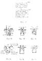
- FIGS. 3 A- 3 Care simplified cross-sectional views of a silicon oxide film at different stages of deposition within a narrow width, high aspect ratio gap according to a prior art silicon oxide deposition process;
- FIGS. 4 A- 4 Care simplified cross-sectional views of a silicon oxide film, deposited according to an embodiment of the present invention, at different stages of deposition within the same narrow width, high aspect ratio gap shown in FIGS. 4 A- 4 C;
- FIGS. 5A and 5Bare a simplified cross-sectional view of the gap-fill capability of a silicon oxide film deposited according to a previously known HDP-CVD process.
- FIGS. 6A and 6Bare a simplified cross-sectional view of the gap-fill capability of a silicon oxide film deposited, according to an embodiment of the present invention, over the same gaps as those shown in FIGS. 5A and 5B.
- Embodiments of the present inventiondeposit an improved silicon oxide layer using high density plasma CVD techniques.
- the deposited layerhas improved gap-fill capabilities as compared to some prior art silicon oxide deposition techniques.
- Films deposited by the method of the present inventionare suitable for use in the fabrication of integrated circuits having feature sizes of 0.18 microns or less.
- Embodiments of the present inventioncan be implemented using a variety of high density plasma CVD substrate processing chambers including chambers in which a plasma is formed by the application of RF energy to a coil that at least partially surrounds a portion of the chamber and chambers that use ECR plasma formation techniques.
- An example of an inductively-coupled HDP-CVD chamber in which embodiments of the method of the present invention can be practicedis set forth below.
- FIG. 1Aillustrates one embodiment of a high density plasma chemical vapor deposition (HDP-CVD) system 10 in which a dielectric layer according to the present invention can be deposited.
- System 10includes a chamber 13 , a vacuum system 70 , a source plasma system 80 A, a bias plasma system 80 B, a gas delivery system 33 , and a remote plasma cleaning system 50 .
- the upper portion of chamber 13includes a dome 14 , which is made of a ceramic dielectric material, such as aluminum oxide or aluminum nitride. Dome 14 defines an upper boundary of a plasma processing region 16 . Plasma processing region 16 is bounded on the bottom by the upper surface of a substrate 17 and a substrate support 18 .
- a heater plate 23 and a cold plate 24surmount, and are thermally coupled to, dome 14 .
- Heater plate 23 and cold plate 24allow control of the dome temperature to within about ⁇ 10° C. over a range of about 100° C. to 200° C. This allows optimizing the dome temperature for the various processes. For example, it may be desirable to maintain the dome at a higher temperature for cleaning or etching processes than for deposition processes. Accurate control of the dome temperature also reduces the flake or particle counts in the chamber and improves adhesion between the deposited layer and the substrate.
- Substrate support 18includes inner and outer passages (not shown) that can deliver a heat transfer gas (sometimes referred to as a backside cooling gas) to the backside of the substrate.
- a heat transfer gassometimes referred to as a backside cooling gas
- the lower portion of chamber 13includes a body member 22 , which joins the chamber to the vacuum system.
- a base portion 21 of substrate support 18is mounted on, and forms a continuous inner surface with, body member 22 .
- Substratesare transferred into and out of chamber 13 by a robot blade (not shown) through an insertion/removal opening (not shown) in the side of chamber 13 .
- Lift pins(not shown) are raised and then lowered under the control of a motor (also not shown) to move the substrate from the robot blade at an upper loading position 57 to a lower processing position 56 in which the substrate is placed on a substrate receiving portion 19 of substrate support 18 .
- Substrate receiving portion 19includes an electrostatic chuck 20 that secures the substrate to substrate support 18 during substrate processing.
- substrate support 18is made from an aluminum oxide or aluminum ceramic material.
- Vacuum system 70includes throttle body 25 , which houses twin-blade throttle valve 26 and is attached to gate valve 27 and turbo-molecular pump 28 .
- throttle body 25offers minimum obstruction to gas flow, and allows symmetric pumping, as described in co-pending, co-assigned U.S. patent application Ser. No. 08/574,839, filed Dec. 12, 1995, and which is incorporated herein by reference.
- Gate valve 27can isolate pump 28 from throttle body 25 , and can also control chamber pressure by restricting the exhaust flow capacity when throttle valve 26 is fully open.
- the arrangement of the throttle valve, gate valve, and turbo-molecular pumpallow accurate and stable control of chamber pressures from between about 1 mTorr to about 2 Torr.
- the source plasma system 80 Aincludes a top coil 29 and side coil 30 , mounted on dome 14 .
- a symmetrical ground shield(not shown) reduces electrical coupling between the coils.
- Top coil 29is powered by top source RF (SRF) generator 31 A
- side coil 30is powered by side SRF generator 31 B, allowing independent power levels and frequencies of operation for each coil.
- SRFsource RF
- This dual coil systemallows control of the radial ion density in chamber 13 , thereby improving plasma uniformity.
- Side coil 30 and top coil 29are typically inductively driven, which does not require a complimentary electrode.
- the top source RF generator 31 Aprovides up to 2,500 watts of RF power at nominally 2 MHz and the side source RF generator 31 B provides up to 5,000 watts of RF power at nominally 2 MHz.
- the operating frequencies of the top and side RF generatorsmay be offset from the nominal operating frequency (e.g. to 1.7-1.9 MHz and 1.9-2.1 MHz, respectively) to improve plasma-generation efficiency.
- a bias plasma system 80 Bincludes a bias RF (BRF) generator 31 C and a bias matching network 32 C.
- the bias plasma system 80 Bcapacitively couples substrate portion 17 to body member 22 , which act as complimentary electrodes.
- the bias plasma system 80 Bserves to enhance the transport of plasma species (e.g., ions) created by the source plasma system 80 A to the surface of the substrate.
- bias RF generatorprovides up to 5,000 watts of RF power at 13.56 MHz.
- RF generators 31 A and 31 Binclude digitally-controlled synthesizers and operate over a frequency range between about 1.8 to about 2.1 MHz. Each generator includes an RF control circuit (not shown) that measures reflected power from the chamber and coil back to the generator and adjusts the frequency of operation to obtain the lowest reflected power, as understood by a person of ordinary skill in the art.
- RF generatorsare typically designed to operate into a load with a characteristic impedance of 50 ohms. RF power may be reflected from loads that have a different characteristic impedance than the generator. This can reduce power transferred to the load. Additionally, power reflected from the load back to the generator may overload and damage the generator.
- the impedance of a plasmamay range from less than 5 ohms to over 900 ohms, depending on the plasma ion density, among other factors, and because reflected power may be a function of frequency, adjusting the generator frequency according to the reflected power increases the power transferred from the RF generator to the plasma and protects the generator. Another way to reduce reflected power and improve efficiency is with a matching network.
- Matching networks 32 A and 32 Bmatch the output impedance of generators 31 A and 31 B with their respective coils 29 and 30 .
- the RF control circuitmay tune both matching networks by changing the value of capacitors within the matching networks to match the generator to the load as the load changes.
- the RF control circuitmay tune a matching network when the power reflected from the load back to the generator exceeds a certain limit.
- One way to provide a constant match, and effectively disable the RF control circuit from tuning the matching networkis to set the reflected power limit above any expected value of reflected power. This may help stabilize a plasma under some conditions by holding the matching network constant at its most recent condition. Other measures may also help stabilize a plasma.
- the RF control circuitcan be used to determine the power delivered to the load (plasma) and may increase or decrease the generator output power to keep the delivered power substantially constant during deposition of a layer.
- a gas delivery system 33provides gases from several sources, 34 A- 34 F chamber for processing the substrate via gas delivery lines 38 (only some of which are shown).
- gas delivery lines 38only some of which are shown.
- the actual sources used for sources 34 A- 34 F and the actual connection of delivery lines 38 to chamber 13varies depending on the deposition and cleaning processes executed within chamber 13 .
- Gasesare introduced into chamber 13 through a gas ring 37 and/or a top nozzle 45 .
- FIG. 1Bis a simplified, partial cross-sectional view of chamber 13 showing additional details of gas ring 37 .
- first and second gas sources, 34 A and 34 B, and first and second gas flow controllers, 35 A′ and 35 B′provide gas to ring plenum 36 in gas ring 37 via gas delivery lines 38 (only some of which are shown).
- Gas ring 37has a plurality of gas nozzles 39 (only one of which is shown for purposes of illustration) that provide a uniform flow of gas over the substrate. Nozzle length and nozzle angle may be changed to allow tailoring of the uniformity profile and gas utilization efficiency for a particular process within an individual chamber.
- gas ring 37has 12 gas nozzles 39 made from an aluminum oxide ceramic.
- Gas ring 37also has a plurality of gas nozzles 40 (only one of which is shown), which in a preferred embodiment are co-planar with and shorter than source gas nozzles 39 , and in one embodiment receive gas from body plenum 41 .
- Gas nozzles 39 and 40are not fluidly coupled in some embodiments it is desirable not to mix gases before injecting the gases into chamber 13 . In other embodiments, gases may be mixed prior to injecting the gases into chamber 13 by providing apertures (not shown) between body plenum 41 and gas ring plenum 36 .
- third and fourth gas sources, 34 C and 34 D, and third and fourth gas flow controllers, 35 C and 35 D′provide gas to body plenum via gas delivery lines 38 . Additional valves, such as 43 B (other valves not shown), may shut off gas from the flow controllers to the chamber.
- valve 43 Bto isolate chamber 13 from delivery line 38 A and to vent delivery line 38 A to vacuum foreline 44 , for example.
- valve 43 A and 43 Cmay be incorporated on other gas delivery lines.
- Such 3-way valvesmay be placed as close to chamber 13 as practical, to minimize the volume of the unvented gas delivery line (between the 3-way valve and the chamber).
- two-way (on-off) valvesmay be placed between a mass flow controller (“MFC”) and the chamber or between a gas source and an MFC.
- MFCmass flow controller
- chamber 13also has top nozzle 45 and top vent 46 .
- Top nozzle 45 and top vent 46allow independent control of top and side flows of the gases, which improves film uniformity and allows fine adjustment of the film's deposition and doping parameters.
- Top vent 46is an annular opening around top nozzle 45 .
- first gas source 34 Asupplies source gas nozzles 39 and top nozzle 45 .
- Source nozzle MFC 35 A′controls the amount of gas delivered to source gas nozzles 39 and top nozzle MFC 35 A controls the amount of gas delivered to top gas nozzle 45 .
- two MFCs 35 B and 35 B′may be used to control the flow of oxygen to both top vent 46 and oxidizer gas nozzles 40 from a single source of oxygen, such as source 34 B.
- the gases supplied to top nozzle 45 and top vent 46may be kept separate prior to flowing the gases into chamber 13 , or the gases may be mixed in top plenum 48 before they flow into chamber 13 . Separate sources of the same gas may be used to supply various portions of the chamber.
- a remote microwave-generated plasma cleaning system 50is provided to periodically clean deposition residues from chamber components.
- the cleaning systemincludes a remote microwave generator 51 that creates a plasma from a cleaning gas source 34 E (e.g., molecular fluorine, nitrogen trifluoride, other fluorocarbons or equivalents) in reactor cavity 53 .
- a cleaning gas source 34 Ee.g., molecular fluorine, nitrogen trifluoride, other fluorocarbons or equivalents
- the reactive species resulting from this plasmaare conveyed to chamber 13 through cleaning gas feed port 54 via applicator tube 55 .
- the materials used to contain the cleaning plasmae.g., cavity 53 and applicator tube 55 ) must be resistant to attack by the plasma.
- the distance between reactor cavity 53 and feed port 54should be kept as short as practical, since the concentration of desirable plasma species may decline with distance from reactor cavity 53 .
- Generating the cleaning plasma in a remote cavityallows the use of an efficient microwave generator and does not subject chamber components to the temperature, radiation, or bombardment of the glow discharge that may be present in a plasma formed in situ. Consequently, relatively sensitive components, such as electrostatic chuck 20 , do not need to be covered with a dummy wafer or otherwise protected, as may be required with an in situ plasma cleaning process.
- System controller 60controls the operation of system 10 .
- controller 60includes a memory 62 , such as a hard disk drive, a floppy disk drive (not shown), and a card rack (not shown) coupled to a processor 61 .
- the card rackmay contain a single-board computer (SBC) (not shown), analog and digital input)output boards (not shown), interface boards (not shown), and stepper motor controller boards (not shown).
- SBCsingle-board computer
- the system controllerconforms to the Versa Modular European (VME) standard, which defines board, card cage, and connector dimensions and types.
- the VME standardalso defines the bus structure as having a 16-bit data bus and 24-bit address bus.
- System controller 60operates under the control of a computer program stored on the hard disk drive or through other computer programs, such as programs stored on a removable disk.
- the computer programdictates, for example, the timing, mixture of gases, RF power levels and other parameters of a particular process.
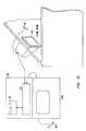
- the interface between a user and the system controlleris via a monitor, such as a cathode ray tube (CRT) 65 , and a light pen 66 , as depicted in FIG. 1C.
- CTRcathode ray tube
- FIG. 1Cis an illustration of a portion of an exemplary system user interface used in conjunction with the exemplary CVD processing chamber of FIG. 1A.
- System controller 60includes a processor 61 coupled to a computer-readable memory 62 .
- memory 62may be a hard disk drive, but memory 62 may be other kinds of memory, such as ROM, PROM, and others.
- System controller 60operates under the control of a computer program 63 stored in a computer-readable format within memory 62 .
- the computer programdictates the timing, temperatures, gas flows, RF power levels and other parameters of a particular process.
- the interface between a user and the system controlleris via a CRT monitor 65 and a light pen 66 , as depicted in FIG. 1C.
- two monitors, 65 and 65 A, and two light pens, 66 and 66 Aare used, one mounted in the clean room wall ( 65 ) for the operators and the other behind the wall ( 65 A) for the service technicians. Both monitors simultaneously display the same information, but only one light pen (e.g. 66 ) is enabled.
- the operatortouches an area of the display screen and pushes a button (not shown) on the pen. The touched area confirms being selected by the light pen by changing its color or displaying a new menu, for example.
- the computer program codecan be written in any conventional computer-readable programming language such as 68000 assembly language, C, C++, or Pascal. Suitable program code is entered into a single file, or multiple files, using a conventional text editor and is stored or embodied in a computer-usable medium, such as a memory system of the computer. If the entered code text is in a high level language, the code is compiled, and the resultant compiler code is then linked with an object code of precompiled windows library routines, To execute the linked compiled object code, the system user invokes the object code causing the computer system to load the code in memory. The CPU reads the code from memory and executes the code to perform the tasks identified in the program.
- a computer-usable mediumsuch as a memory system of the computer.
- FIG. 1Dshows an illustrative block diagram of the hierarchical control structure of computer program 100 .
- a userenters a process set number and process chamber number into a process selector subroutine 110 in response to menus or screens displayed on the CRT monitor by using the light pen interface.
- the process setsare predetermined sets of process parameters necessary to carry out specified processes, and are identified by predefined set numbers.
- Process selector subroutine 110identifies (i) the desired process chamber in a multichamber system, and (ii) the desired set of process parameters needed to operate the process chamber for performing the desired process.
- the process parameters for performing a specific processrelate to conditions such as process gas composition and flow rates, temperature, pressure, plasma conditions such as RF power levels, and chamber dome temperature, and are provided to the user in the form of a recipe.
- the parameters specified by the recipeare entered utilizing the light pen/CRT monitor interface.
- the signals for monitoring the processare provided by the analog and digital input boards of system controller 60 , and the signals for controlling the process are output on the analog and digital output boards of system controller 60 .
- a process sequencer subroutine 120comprises program code for accepting the identified process chamber and set of process parameters from the process selector subroutine 110 and for controlling operation of the various process chambers. Multiple users can enter process set numbers and process chamber numbers, or a single user can enter multiple process set numbers and process chamber numbers; sequencer subroutine 120 schedules the selected processes in the desired sequence.
- sequencer subroutine 120includes a program code to perform the steps of (i) monitoring the operation of the process chambers to determine if the chambers are being used, (ii) determining what processes are being carried out in the chambers being used, and (iii) executing the desired process based on availability of a process chamber and type of process to be carried out.
- sequencer subroutine 120can be designed to take into consideration the “age of each particular user-entered request, or the present condition of the process chamber being used in comparison with the desired process conditions for a selected process, or any other relevant factor a system programmer desires to include for determining scheduling priorities.
- sequencer subroutine 120determines which process chamber and process set combination is going to be executed next, sequencer subroutine 120 initiates execution of the process set by passing the particular process set parameters to a chamber manager subroutine 130 A-C, which controls multiple processing tasks in chamber 13 and possibly other chambers (not shown) according to the process set sent by sequencer subroutine 120 .
- chamber component subroutinesare substrate positioning subroutine 140 , process gas control subroutine 150 , pressure control subroutine 160 , and plasma control subroutine 170 .
- chamber manager subroutine 130 Aselectively schedules or calls the process component subroutines in accordance with the particular process set being executed.
- Chamber manager subroutine 130 Aschedules process component subroutines in the same manner that sequencer subroutine 120 schedules the process chamber and process set to execute.
- chamber manager subroutine 130 Aincludes steps of monitoring the various chamber components, determining which components need to be operated based on the process parameters for the process set to be executed, and causing execution of a chamber component subroutine responsive to the monitoring and determining steps.
- Substrate positioning subroutine 140comprises program code for controlling chamber components that are used to load a substrate onto substrate support number 18 .
- Substrate positioning subroutine 140may also control transfer of a substrate into chamber 13 from, e.g., a PECVD reactor or other reactor in the multi-chamber system, after other processing has been completed.
- Process gas control subroutine 150has program code for controlling process gas composition and flow rates. Subroutine 150 controls the open/close position of the safety shut-off valves and also ramps up/ramps down the mass flow controllers to obtain the desired gas flow rates. All chamber component subroutines, including process gas control subroutine 150 , are invoked by chamber manager subroutine 130 A. Subroutine 150 receives process parameters from chamber manager subroutine 130 A related to the desired gas flow rates.
- process gas control subroutine 150opens the gas supply lines, and repeatedly (i) reads the necessary mass flow controllers, (ii) compares the readings to the desired flow rates received from chamber manager subroutine 130 A, and (iii) adjusts the flow rates of the gas supply lines as necessary. Furthermore, process gas control subroutine 150 may include steps for monitoring the gas flow rates for unsafe rates and for activating the safety shut-off valves when an unsafe condition is detected.
- an inert gassuch as argon
- the process gas control subroutine 150is programmed to include steps for flowing the inert gas into chamber 13 for an amount of time necessary to stabilize the pressure in the chamber. The steps described above may then be carried out.
- the process gas control subroutine 150may include steps for bubbling a delivery gas such as helium through the liquid precursor in a bubbler assembly or for introducing the helium to a liquid injection valve.
- a delivery gassuch as helium
- the process gas control subroutine 150regulates the flow of the delivery gas, the pressure in the bubbler, and the bubbler temperature to obtain the desired process gas flow rates.
- the desired process gas flow ratesare transferred to process gas control subroutine 150 as process parameters.
- the process gas control subroutine 150includes steps for obtaining the necessary delivery gas flow rate, bubbler pressure, and bubbler temperature for the desired process gas flow rate by accessing a stored table containing the necessary values for a given process gas flow rate. Once the necessary values are obtained, the delivery gas flow rate, bubbler pressure and bubbler temperature are monitored, compared to the necessary values and adjusted accordingly.
- the process gas control subroutine 150may also control the flow of heat-transfer gas, such as helium (He), through the inner and outer passages in the wafer chuck with an independent helium control (IHC) subroutine (not shown).
- the gas flowthermally couples the substrate to the chuck.
- the waferis heated by the plasma and the chemical reactions that form the layer, and the He cools the substrate through the chuck, which may be water-cooled. This keeps the substrate below a temperature that may damage preexisting features on the substrate.
- Pressure control subroutine 160includes program code for controlling the pressure in chamber 13 by regulating the size of the opening of throttle valve 26 in the exhaust portion of the chamber.
- the first methodrelies on characterizing the chamber pressure as it relates to, among other things, the total process gas flow, the size of the process chamber, and the pumping capacity.
- the first methodsets throttle valve 26 to a fixed position. Setting throttle valve 26 to a fixed position may eventually result in a steady-state pressure.
- the chamber pressuremay be measured, with a manometer for example, and the position of throttle valve 26 may be adjusted according to pressure control subroutine 160 , assuming the control point is within the boundaries set by gas flows and exhaust capacity.
- the former methodmay result in quicker chamber pressure changes, as the measurements, comparisons, and calculations associated with the latter method are not invoked.
- the former methodmay be desirable where precise control of the chamber pressure is not required, whereas the latter method may be desirable where an accurate, repeatable, and stable pressure is desired, such as during the deposition of a layer.
- pressure control subroutine 160When pressure control subroutine 160 is invoked, the desired, or target, pressure level is received as a parameter from chamber manager subroutine 130 A. Pressure control subroutine 160 measures the pressure in chamber 13 by reading one or more conventional pressure manometers connected to the chamber; compares the measured value(s) to the target pressure; obtains proportional, integral, and differential (PID) values from a stored pressure table corresponding to the target pressure, and adjusts throttle valve 26 according to the PID values obtained from the pressure table. Alternatively, pressure control subroutine 160 may open or close throttle valve 26 to a particular opening size to regulate the pressure in chamber 13 to a desired pressure or pressure range.
- PIDproportional, integral, and differential
- Plasma control subroutine 170comprises program code for controlling the frequency and power output setting of RF generators 31 A and 31 B and for tuning matching networks 32 A and 32 B.
- Plasma control subroutine 170like the previously described chamber component subroutines, is invoked by chamber manager subroutine 130 A.
- FIG. 2illustrates one particular embodiment of the invention as used to deposit a silicon oxide film over a semiconductor substrate.
- the processis for exemplary purposes and is not intended to limit the scope of the claims of the present invention. Where applicable, reference numbers in the description below are used to refer to appropriate components of the exemplary chamber of FIGS. 1 A- 1 D. In this embodiment the process is implemented and controlled using a computer program stored in the memory 62 of system controller 60 .
- the method shown in FIG. 2deposits an undoped silicon oxide layer by flowing a process gas into chamber 1 (step 200 ) and forming a plasma from the process gas (step 205 ).
- the length of the deposition processis determined by the desired thickness of the silicon oxide film.
- One manner in which the deposition process shown in FIG. 2 differs from previous HDP-CVD silicon oxide deposition processesis by adding a flow of a hydrogen-containing source to the traditional silicon oxide deposition gas.
- a hydrogen-containing sourcee.g., SiH 4 , Si 2 H 6 , etc.
- an oxygen-containing sourcee.g., O 2
- an inert gase.g., Ar
- deposition conditions for such a silicon oxide filmare carefully controlled in order to minimize the amount of hydrogen incorporated into the film because as is known to those of skill in the art, hydrogen is a source of film instability.
- the hydrogen-containing gascan be one or more of the following: molecular hydrogen (H 2 ), water (H 2 O), ammonia (NH 3 ), methane (CH 4 ), ethane (C 2 H 6 ) or another hydride gas that does not include silicon, boron or phosphorus.
- the process gasconsists of SiH 4 , O 2 , Ar and H 2 .
- the first numberindicates the flow rate of the particular gas through side nozzles 39 , 40 while the second number indicates the flow rate of the gas through top nozzle 45 .
- TVOmeans “throttle valve fully open” which results in chamber pressure being controlled by the quantity of gas flowed into the chamber.
- FIGS. 3 A- 3 Cwhich are simplified cross-sectional views of a silicon oxide film at different stages of deposition, illustrate the potential gap-fill limitation that is associated with the process recipe of Table 1 for certain small width gaps having relatively high aspect ratios. It is important to understand that while HDP-CVD silicon oxide deposition techniques generally provide for improved gap-fill as compared to other plasma silicon oxide deposition techniques including low density, capacitively coupled plasma CVD techniques, the gap-fill issues associated with those techniques become an issue for HDP-CVD techniques in certain aggressive gap-fill applications, for example, gaps having a width of 0.1 ⁇ m and a 5:1 aspect ratio. The gap-fill problem illustrated in FIGS. 3 A- 3 C is somewhat exaggerated in order to better illustrate the problem.
- FIG. 3Ashows the initial stages of film deposition over a substrate (not shown) having a gap 220 defined by two adjacent features 222 , 224 formed over the substrate.
- the conventional HDP-CVD silicon oxide deposition processresults in direct silicon oxide deposition on horizontal surface 226 within gap 220 and horizontal surfaces 228 above features 222 , 224 .
- the processalso results in indirect deposition (referred to as re-deposition) of silicon oxide on sidewalls 230 due to the recombination of material sputtered from the silicon oxide film as it grows.
- the continued growth of the silicon oxide filmresults in formations 232 on the upper section gap sidewall that grow toward each other at a rate of growth exceeding the rate at which the film grows laterally on lower portions 234 of the sidewall (see FIG. 3B also).
- the final result of this processis that a void 236 forms as shown in FIG. 3C.
- FIGS. 4 A- 4 Cillustrate how a film deposited according to the process of FIG. 2 is able to completely fill a gap 240 where the film of Table 1 was not capable of filling the gap in a void-free manner.
- FIGS. 4 A- 4 Crepresents growth of the silicon oxide film deposited according to FIG. 2 at the same point in the deposition process as the corresponding one of FIGS. 3 A- 3 C.
- FIGS. 3A and 4Amay represent film growth after 10 seconds. It is important to note, however, that none of FIGS. 3 A- 3 C or 4 A- 4 C are intended to be drawn to scale and the actual aspect ratio of the gaps represented in these figures is higher than it appears to be if measuring the figures.
- an HDP-CVD silicon oxide film deposited according to the process of FIG. 2grows on a horizontal surface 244 within gap 240 at approximately the same rate as the film discussed with respect to FIG. 3A.
- Film growth on horizontal surfaces 246 on top of feature 242is slower than film growth on surfaces 228 in FIG. 3A.
- film growth or re-deposition on an upper portion 248 of the gap sidewallis glower than in FIG. 3A.
- This reactionreduces the amount of O sputtering, which in turn reduces SiO 2 deposition on the sidewall because sidewall deposition, especially for trenches with a vertical sidewall, is largely initiated by sputter re-deposition. Thus less SiO 2 is deposited on the sidewall than in processes that do not employ the techniques of the present invention.
- the ratio of the flow rate of the oxygen-containing source to the combined flow rate of the silane gas and hydrogen-containing gas in some embodimentsshould be between 1.6 and 2.5 to 1 inclusive. At ratios below 1.6:1 the silicon oxide film becomes silicon rich, exhibits poor electrical breakdown characteristics and has an undesirably high refractive index. At ratios above 1.6:1, the relatively high gas flow rates required to achieve such ratios increases the chamber pressure to undesirably high levels which in turn degrades film gap-fill capabilities.
- the ratio of the flow rate of the hydrogen-containing gas to the silane gas in some embodimentsshould be between 0.5-2.0:1 inclusive. At ratios below 0.5:1, not enough additional hydrogen is introduced to achieve desirable gap-fill benefits, and at ratios higher than 2.0:1, the relatively high gas flow rates required to achieve such ratios increases the chamber pressure to undesirably high levels which in turn degrades film gap-fill capabilities.
- the method of the present inventionis particularly useful for the deposition of undoped silicon oxide layers for PMD and STI applications. Each of these applications often involve gap-fill requirements that are more aggressive, i.e., higher aspect ratio gaps, than IMD applications.
- the deposition process of many embodiments of the inventionoccurs at a substrate temperature above 450° C. and more typically between 500° C. and 750° C.
- Films deposited according to these embodimentsgenerally have a hydrogen content, as measured by Auger analysis, of between 1.5-1.6 atomic percent. This is comparable to about 1.5 at. % hydrogen content of a standard HDP-CVD USG film deposited from a process gas of SiH 4 , O 2 and Ar using the parameters of Table 1.
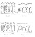
- FIGS. 6A and 6Billustrates the benefits of a deposition process according to FIG. 2 as compared to a process according to Table 1.
- FIGS. 5A and 5Bare a simplified cross-sectional view of a silicon oxide film deposited according to the process of Table 1.
- the filmis deposited over a substrate having multiple sets of raised features defining 0.15 ⁇ m wide gaps 260 and 0.17 ⁇ m wide gaps 262 .
- the height of gaps 260 and 262is 0.7 ⁇ m so the aspect ratio of gaps 260 is approximately 4.7:1 while the aspect ratio of gaps 262 is approximately 4.1:1.
- FIG. 5Athe film is deposited over a substrate having multiple sets of raised features defining 0.15 ⁇ m wide gaps 260 and 0.17 ⁇ m wide gaps 262 .
- the height of gaps 260 and 262is 0.7 ⁇ m so the aspect ratio of gaps 260 is approximately 4.7:1 while the aspect ratio of gaps 262 is approximately 4.1:1.
- the silicon oxide filmis not able to completely fill gaps 260 without the formation of voids 264 within the gaps. Similarly, while no voids are formed within gaps 262 , the deposition process results in a surface topology that includes unfilled areas 266 near the upper strata of gap 262 .
- FIG. 6Ashows deposition of an HDP-CVD silicon oxide film according to the process of FIG. 2 over 0.15 ⁇ m and 0.17 ⁇ m gaps 270 and 272 having aspect ratios identical to the respective gaps in FIG. 5A.
- the film deposited according to the process of FIG. 2has superior gap-fill capabilities as compared to the film of FIG. 5A.
- Gaps 272are completely filled without voids and voids 274 within gaps 270 are smaller than voids 264 within gaps 260 .
- FIG. 6BFurther evidence of the superiority of the process of FIG. 2 as compared to that of Table 1 is evident from a comparison of FIG. 6B to FIG. 5B.
- the substrates shown in FIGS. 5B and 6Binclude trenches 280 having a widths of 0.1 ⁇ m at the top of the trench and a width as low as 0.02 ⁇ m at the bottom of the trench.
- the midpoint 282 of trenches 280has a width of about 0.05 ⁇ m and the height of the trenches is 0.4 ⁇ m.
- the aspect ratio of trenches 280is 8.0:1.
- the film deposited according to the process of FIG. 2does not include any voids within the gaps and thus has superior gap-fill capabilities as compared to the film deposited according to the process of Table 1 (FIG. 5B).
Landscapes
- Engineering & Computer Science (AREA)
- Chemical & Material Sciences (AREA)
- Manufacturing & Machinery (AREA)
- General Physics & Mathematics (AREA)
- Physics & Mathematics (AREA)
- Computer Hardware Design (AREA)
- Microelectronics & Electronic Packaging (AREA)
- Power Engineering (AREA)
- Condensed Matter Physics & Semiconductors (AREA)
- Inorganic Chemistry (AREA)
- General Chemical & Material Sciences (AREA)
- Chemical Kinetics & Catalysis (AREA)
- Materials Engineering (AREA)
- Mechanical Engineering (AREA)
- Metallurgy (AREA)
- Organic Chemistry (AREA)
- Formation Of Insulating Films (AREA)
- Chemical Vapour Deposition (AREA)
Abstract
Description
- The present invention relates to the manufacture of integrated circuits. More specifically, the invention relates to an improved method of depositing silicon oxide layers for use as insulation layers in such integrated circuits.[0001]
- One of the primary steps in the fabrication of modern semiconductor devices is the formation of a film, such as a silicon oxide, on a semiconductor substrate. Silicon oxide is widely used as an insulating layer in the manufacture of semiconductor devices. As is well known, a silicon oxide film can be deposited by thermal chemical vapor deposition (CVD) or a plasma-enhanced chemical vapor deposition (PECVD) processes. In a conventional thermal CVD process, reactive gases are supplied to the substrate surface where heat-induced chemical reactions (homogeneous or heterogeneous) take place to produce a desired film. In a conventional plasma process, a controlled plasma is formed to decompose and/or energize reactive species to produce the desired film.[0002]
- Semiconductor device geometries have dramatically decreased in size since such devices were first introduced several decades ago. Smaller feature sizes have resulted in the presence of increased aspect ratio gaps for some applications, for example, between adjacent conductive lines or in etched trenches. The aspect ratio of a gap is defined by the ratio of the gap's height or depth to its width. These spaces are difficult to fill using conventional CVD methods. A film's ability to completely fill such gaps is referred to as the film's “gap-filling” ability. Silicon oxide is one type of insulation film that is commonly used to fill the gaps in intermetal dielectric (IMD) applications, premetal dielectric (PMD) applications and shallow trench isolation (STI) applications among others. Such a silicon oxide film is often referred to as a gap-fill film or a gap-fill layer.[0003]
- Some integrated circuit manufacturers have turned to the use of high density plasma CVD (HDP-CVD) systems to deposit silicon oxide gap-fill layers. HDP-CVD systems form a plasma that is approximately two orders of magnitude or greater than the density of a standard, capacitively-coupled plasma CVD system. Examples of HDP-CVD systems include inductively-coupled plasma systems and electron cyclotron resonance (ECR) plasma systems among others. HDP-CVD systems generally operate at lower pressure ranges than low density plasma systems. The low chamber pressure employed in HDP-CVD systems provides active species having a long mean-free-path and reduced angular distribution. These factors, in combination with the plasma's density, contribute to a significant number of constituents from the plasma reaching even the deepest portions of closely spaced gaps, providing a film with improved gap-fill capabilities as compared to films deposited in a low density plasma CVD system.[0004]
- Another factor that allows films deposited by HDP-CVD techniques to have improved gap-fill characteristics as compared to films deposited by other CVD techniques is the occurrence of sputtering, promoted by the plasma's high density, simultaneous with film deposition. The sputtering element of HDP deposition slows deposition on certain features, such as the comers of raised surfaces, thereby contributing to the increased gap-fill ability of HDP deposited films. Some HDP-CVD systems introduce argon or a similar heavy inert gas to further promote the sputtering effect. These HDP-CVD systems typically employ an electrode within the substrate support pedestal that enables the creation of an electric field to bias the plasma toward the substrate. The electric field can be applied throughout the HDP deposition process to further promote sputtering and provide better gap-fill characteristics for a given film.[0005]
- One HDP-CVD process commonly used to deposit a silicon oxide film forms a plasma from a process gas that includes silane (SiH[0006]4), molecular oxygen (O2) and argon (Ar). This silicon oxide film has improved gap-fill characteristics as opposed to some silicon oxide films deposited by other non-HDP-CVD plasma techniques and is useful for a variety of applications. Despite the improvement in gap-fill capability provided by HDP-CVD systems and the relatively good gap-fill characteristics of HDP-CVD silicon oxide films in particular, the development of film deposition techniques that enable the deposition of silicon oxide layers having even further improved gap-fill characteristics are desirable. Such improved silicon oxide film deposition are particularly desirable in light of the aggressive gap-fill challenges presented by integrated circuit designs employing minimum feature sizes of 0.18 microns and less.
- Embodiments of the present invention pertain to an improved method of depositing silicon oxide films using HDP-CVD deposition techniques. These embodiments enable improved gap-fill capabilities as compared to HDP-CVD silicon oxide deposition techniques that do not employ the method of the present invention and the embodiments are useful for the manufacture of integrated circuits having minimum feature sizes of 0.18 microns or less.[0007]
- In one embodiment, the present invention forms an undoped silicon oxide layer (USG) over a substrate disposed in a high density plasma substrate processing chamber. The silicon oxide layer is formed by flowing a process gas into the substrate processing chamber and forming a high density plasma (i.e., a plasma having an ion density of at least 1×10[0008]11ions/cm3) from the process gas to deposit said silicon oxide layer over said substrate. The process gas includes a silane gas, an oxygen-containing source, an inert gas and a hydrogen-containing source that is selected from the group of H2, H2O, NH3, CH4, C2H6, or a hydride gas that does not include silicon, boron or phosphorus. The deposited silicon oxide layer has a hydrogen content of less than or equal to 2 atomic percent.
- In another embodiment, the present invention forms an undoped silicon oxide layer (USG) from a process gas consisting of SiH[0009]4, O2, Ar and H2. The flow rate ratio of O2to the combined flow of SiH4and H2in the process gas is between 1.6-2.5:1 inclusive and the flow rate ratio of H2to SiH4is between 0.5-2.0:1 inclusive. The process gas is flowed into the substrate processing chamber and a high density plasma is formed from the process gas to deposit the silicon oxide layer over the substrate. The deposited silicon oxide layer has a dielectric constant of between 4.0 and 4.2 and contains less than or equal to 2 atomic percent hydrogen.
- These and other embodiments of the present invention, as well as its advantages and features are described in more detail in conjunction with the text below and attached figures.[0010]
- FIG. 1A is a simplified diagram of one embodiment of a high density chemical vapor deposition system according to the present invention;[0011]
- FIG. 1B is a simplified cross section of a gas ring that may be used in conjunction with the exemplary CVD processing chamber of FIG. 1A;[0012]
- FIG. 1C is a simplified diagram of a monitor and light pen that may be used in conjunction with the exemplary CVD processing chamber of FIG. 1A;[0013]
- FIG. 1D is a flow chart of an exemplary process control computer program product used to control the exemplary CVD processing chamber of FIG. 1A;[0014]
- FIG. 2 is a flowchart illustrating one embodiment of the method of the present invention;[0015]
- FIGS.[0016]3A-3C are simplified cross-sectional views of a silicon oxide film at different stages of deposition within a narrow width, high aspect ratio gap according to a prior art silicon oxide deposition process;
- FIGS.[0017]4A-4C are simplified cross-sectional views of a silicon oxide film, deposited according to an embodiment of the present invention, at different stages of deposition within the same narrow width, high aspect ratio gap shown in FIGS.4A-4C;
- FIGS. 5A and 5B are a simplified cross-sectional view of the gap-fill capability of a silicon oxide film deposited according to a previously known HDP-CVD process; and[0018]
- FIGS. 6A and 6B are a simplified cross-sectional view of the gap-fill capability of a silicon oxide film deposited, according to an embodiment of the present invention, over the same gaps as those shown in FIGS. 5A and 5B.[0019]
- I. Introduction[0020]
- Embodiments of the present invention deposit an improved silicon oxide layer using high density plasma CVD techniques. The deposited layer has improved gap-fill capabilities as compared to some prior art silicon oxide deposition techniques. Films deposited by the method of the present invention are suitable for use in the fabrication of integrated circuits having feature sizes of 0.18 microns or less.[0021]
- Embodiments of the present invention can be implemented using a variety of high density plasma CVD substrate processing chambers including chambers in which a plasma is formed by the application of RF energy to a coil that at least partially surrounds a portion of the chamber and chambers that use ECR plasma formation techniques. An example of an inductively-coupled HDP-CVD chamber in which embodiments of the method of the present invention can be practiced is set forth below.[0022]
- II. Exemplary Substrate Processing System[0023]
- FIG. 1A illustrates one embodiment of a high density plasma chemical vapor deposition (HDP-CVD)[0024]
system 10 in which a dielectric layer according to the present invention can be deposited.System 10 includes achamber 13, a vacuum system70, asource plasma system 80A, a bias plasma system80B, agas delivery system 33, and a remote plasma cleaning system50. - The upper portion of[0025]
chamber 13 includes a dome14, which is made of a ceramic dielectric material, such as aluminum oxide or aluminum nitride. Dome14 defines an upper boundary of a plasma processing region16. Plasma processing region16 is bounded on the bottom by the upper surface of asubstrate 17 and asubstrate support 18. - A[0026]
heater plate 23 and acold plate 24 surmount, and are thermally coupled to, dome14.Heater plate 23 andcold plate 24 allow control of the dome temperature to within about ±10° C. over a range of about 100° C. to 200° C. This allows optimizing the dome temperature for the various processes. For example, it may be desirable to maintain the dome at a higher temperature for cleaning or etching processes than for deposition processes. Accurate control of the dome temperature also reduces the flake or particle counts in the chamber and improves adhesion between the deposited layer and the substrate. - Generally, exposure to the plasma heats a substrate positioned on[0027]
substrate support 18.Substrate support 18 includes inner and outer passages (not shown) that can deliver a heat transfer gas (sometimes referred to as a backside cooling gas) to the backside of the substrate. - The lower portion of[0028]
chamber 13 includes abody member 22, which joins the chamber to the vacuum system. Abase portion 21 ofsubstrate support 18 is mounted on, and forms a continuous inner surface with,body member 22. Substrates are transferred into and out ofchamber 13 by a robot blade (not shown) through an insertion/removal opening (not shown) in the side ofchamber 13. Lift pins (not shown) are raised and then lowered under the control of a motor (also not shown) to move the substrate from the robot blade at anupper loading position 57 to a lower processing position56 in which the substrate is placed on asubstrate receiving portion 19 ofsubstrate support 18.Substrate receiving portion 19 includes anelectrostatic chuck 20 that secures the substrate tosubstrate support 18 during substrate processing. In a preferred embodiment,substrate support 18 is made from an aluminum oxide or aluminum ceramic material. - Vacuum system[0029]70 includes
throttle body 25, which houses twin-blade throttle valve 26 and is attached togate valve 27 and turbo-molecular pump 28. It should be noted thatthrottle body 25 offers minimum obstruction to gas flow, and allows symmetric pumping, as described in co-pending, co-assigned U.S. patent application Ser. No. 08/574,839, filed Dec. 12, 1995, and which is incorporated herein by reference.Gate valve 27 can isolate pump28 fromthrottle body 25, and can also control chamber pressure by restricting the exhaust flow capacity whenthrottle valve 26 is fully open. The arrangement of the throttle valve, gate valve, and turbo-molecular pump allow accurate and stable control of chamber pressures from between about 1 mTorr to about 2 Torr. - The[0030]
source plasma system 80A includes atop coil 29 and side coil30, mounted on dome14. A symmetrical ground shield (not shown) reduces electrical coupling between the coils.Top coil 29 is powered by top source RF (SRF)generator 31A, whereas side coil30 is powered byside SRF generator 31B, allowing independent power levels and frequencies of operation for each coil. This dual coil system allows control of the radial ion density inchamber 13, thereby improving plasma uniformity. Side coil30 andtop coil 29 are typically inductively driven, which does not require a complimentary electrode. In a specific embodiment, the topsource RF generator 31A provides up to 2,500 watts of RF power at nominally 2 MHz and the sidesource RF generator 31B provides up to 5,000 watts of RF power at nominally 2 MHz. The operating frequencies of the top and side RF generators may be offset from the nominal operating frequency (e.g. to 1.7-1.9 MHz and 1.9-2.1 MHz, respectively) to improve plasma-generation efficiency. - A bias plasma system[0031]80B includes a bias RF (BRF) generator31C and a
bias matching network 32C. The bias plasma system80B capacitively couplessubstrate portion 17 tobody member 22, which act as complimentary electrodes. The bias plasma system80B serves to enhance the transport of plasma species (e.g., ions) created by thesource plasma system 80A to the surface of the substrate. In a specific embodiment, bias RF generator provides up to 5,000 watts of RF power at 13.56 MHz. - [0032]
RF generators - [0033]
Matching networks generators respective coils 29 and30. The RF control circuit may tune both matching networks by changing the value of capacitors within the matching networks to match the generator to the load as the load changes. The RF control circuit may tune a matching network when the power reflected from the load back to the generator exceeds a certain limit. One way to provide a constant match, and effectively disable the RF control circuit from tuning the matching network, is to set the reflected power limit above any expected value of reflected power. This may help stabilize a plasma under some conditions by holding the matching network constant at its most recent condition. Other measures may also help stabilize a plasma. For example, the RF control circuit can be used to determine the power delivered to the load (plasma) and may increase or decrease the generator output power to keep the delivered power substantially constant during deposition of a layer. - A[0034]
gas delivery system 33 provides gases from several sources,34A-34F chamber for processing the substrate via gas delivery lines38 (only some of which are shown). As would be understood by a person of skill in the art, the actual sources used forsources 34A-34F and the actual connection ofdelivery lines 38 tochamber 13 varies depending on the deposition and cleaning processes executed withinchamber 13. Gases are introduced intochamber 13 through agas ring 37 and/or a top nozzle45. FIG. 1B is a simplified, partial cross-sectional view ofchamber 13 showing additional details ofgas ring 37. - In one embodiment, first and second gas sources,[0035]34A and34B, and first and second gas flow controllers,35A′ and35B′, provide gas to ring
plenum 36 ingas ring 37 via gas delivery lines38 (only some of which are shown).Gas ring 37 has a plurality of gas nozzles39 (only one of which is shown for purposes of illustration) that provide a uniform flow of gas over the substrate. Nozzle length and nozzle angle may be changed to allow tailoring of the uniformity profile and gas utilization efficiency for a particular process within an individual chamber. In a preferred embodiment,gas ring 37 has12gas nozzles 39 made from an aluminum oxide ceramic. - [0036]
Gas ring 37 also has a plurality of gas nozzles40 (only one of which is shown), which in a preferred embodiment are co-planar with and shorter thansource gas nozzles 39, and in one embodiment receive gas from body plenum41.Gas nozzles chamber 13. In other embodiments, gases may be mixed prior to injecting the gases intochamber 13 by providing apertures (not shown) between body plenum41 andgas ring plenum 36. In one embodiment, third and fourth gas sources,34C and34D, and third and fourth gas flow controllers,35C and35D′, provide gas to body plenum via gas delivery lines38. Additional valves, such as43B (other valves not shown), may shut off gas from the flow controllers to the chamber. - In embodiments where flammable, toxic, or corrosive gases are used, it may be desirable to eliminate gas remaining in the gas delivery lines after a deposition. This may be accomplished using a 3-way valve, such as[0037]
valve 43B, to isolatechamber 13 fromdelivery line 38A and to ventdelivery line 38A to vacuumforeline 44, for example. As shown in FIG. 1A, other similar valves, such as43A and43C, may be incorporated on other gas delivery lines. Such 3-way valves may be placed as close tochamber 13 as practical, to minimize the volume of the unvented gas delivery line (between the 3-way valve and the chamber). Additionally, two-way (on-off) valves (not shown) may be placed between a mass flow controller (“MFC”) and the chamber or between a gas source and an MFC. - Referring again to FIG. 1A,[0038]
chamber 13 also has top nozzle45 andtop vent 46. Top nozzle45 andtop vent 46 allow independent control of top and side flows of the gases, which improves film uniformity and allows fine adjustment of the film's deposition and doping parameters.Top vent 46 is an annular opening around top nozzle45. In one embodiment,first gas source 34A suppliessource gas nozzles 39 and top nozzle45.Source nozzle MFC 35A′ controls the amount of gas delivered to sourcegas nozzles 39 andtop nozzle MFC 35A controls the amount of gas delivered to top gas nozzle45. Similarly, twoMFCs top vent 46 andoxidizer gas nozzles 40 from a single source of oxygen, such assource 34B. The gases supplied to top nozzle45 andtop vent 46 may be kept separate prior to flowing the gases intochamber 13, or the gases may be mixed intop plenum 48 before they flow intochamber 13. Separate sources of the same gas may be used to supply various portions of the chamber. - A remote microwave-generated plasma cleaning system[0039]50 is provided to periodically clean deposition residues from chamber components. The cleaning system includes a
remote microwave generator 51 that creates a plasma from a cleaninggas source 34E (e.g., molecular fluorine, nitrogen trifluoride, other fluorocarbons or equivalents) inreactor cavity 53. The reactive species resulting from this plasma are conveyed tochamber 13 through cleaning gas feed port54 viaapplicator tube 55. The materials used to contain the cleaning plasma (e.g.,cavity 53 and applicator tube55) must be resistant to attack by the plasma. The distance betweenreactor cavity 53 and feed port54 should be kept as short as practical, since the concentration of desirable plasma species may decline with distance fromreactor cavity 53. Generating the cleaning plasma in a remote cavity allows the use of an efficient microwave generator and does not subject chamber components to the temperature, radiation, or bombardment of the glow discharge that may be present in a plasma formed in situ. Consequently, relatively sensitive components, such aselectrostatic chuck 20, do not need to be covered with a dummy wafer or otherwise protected, as may be required with an in situ plasma cleaning process. - [0040]
System controller 60 controls the operation ofsystem 10. In a preferred embodiment,controller 60 includes amemory 62, such as a hard disk drive, a floppy disk drive (not shown), and a card rack (not shown) coupled to aprocessor 61. The card rack may contain a single-board computer (SBC) (not shown), analog and digital input)output boards (not shown), interface boards (not shown), and stepper motor controller boards (not shown). The system controller conforms to the Versa Modular European (VME) standard, which defines board, card cage, and connector dimensions and types. The VME standard also defines the bus structure as having a 16-bit data bus and 24-bit address bus.System controller 60 operates under the control of a computer program stored on the hard disk drive or through other computer programs, such as programs stored on a removable disk. The computer program dictates, for example, the timing, mixture of gases, RF power levels and other parameters of a particular process. The interface between a user and the system controller is via a monitor, such as a cathode ray tube (CRT)65, and alight pen 66, as depicted in FIG. 1C. - FIG. 1C is an illustration of a portion of an exemplary system user interface used in conjunction with the exemplary CVD processing chamber of FIG. 1A.[0041]
System controller 60 includes aprocessor 61 coupled to a computer-readable memory 62. Preferably,memory 62 may be a hard disk drive, butmemory 62 may be other kinds of memory, such as ROM, PROM, and others. - [0042]
System controller 60 operates under the control of acomputer program 63 stored in a computer-readable format withinmemory 62. The computer program dictates the timing, temperatures, gas flows, RF power levels and other parameters of a particular process. The interface between a user and the system controller is via aCRT monitor 65 and alight pen 66, as depicted in FIG. 1C. In a preferred embodiment, two monitors,65 and65A, and two light pens,66 and66A, are used, one mounted in the clean room wall (65) for the operators and the other behind the wall (65A) for the service technicians. Both monitors simultaneously display the same information, but only one light pen (e.g.66) is enabled. To select a particular screen or function, the operator touches an area of the display screen and pushes a button (not shown) on the pen. The touched area confirms being selected by the light pen by changing its color or displaying a new menu, for example. - The computer program code can be written in any conventional computer-readable programming language such as 68000 assembly language, C, C++, or Pascal. Suitable program code is entered into a single file, or multiple files, using a conventional text editor and is stored or embodied in a computer-usable medium, such as a memory system of the computer. If the entered code text is in a high level language, the code is compiled, and the resultant compiler code is then linked with an object code of precompiled windows library routines, To execute the linked compiled object code, the system user invokes the object code causing the computer system to load the code in memory. The CPU reads the code from memory and executes the code to perform the tasks identified in the program.[0043]
- FIG. 1D shows an illustrative block diagram of the hierarchical control structure of[0044]
computer program 100. A user enters a process set number and process chamber number into aprocess selector subroutine 110 in response to menus or screens displayed on the CRT monitor by using the light pen interface. The process sets are predetermined sets of process parameters necessary to carry out specified processes, and are identified by predefined set numbers.Process selector subroutine 110 identifies (i) the desired process chamber in a multichamber system, and (ii) the desired set of process parameters needed to operate the process chamber for performing the desired process. The process parameters for performing a specific process relate to conditions such as process gas composition and flow rates, temperature, pressure, plasma conditions such as RF power levels, and chamber dome temperature, and are provided to the user in the form of a recipe. The parameters specified by the recipe are entered utilizing the light pen/CRT monitor interface. - The signals for monitoring the process are provided by the analog and digital input boards of[0045]
system controller 60, and the signals for controlling the process are output on the analog and digital output boards ofsystem controller 60. - A[0046]
process sequencer subroutine 120 comprises program code for accepting the identified process chamber and set of process parameters from theprocess selector subroutine 110 and for controlling operation of the various process chambers. Multiple users can enter process set numbers and process chamber numbers, or a single user can enter multiple process set numbers and process chamber numbers;sequencer subroutine 120 schedules the selected processes in the desired sequence. Preferably,sequencer subroutine 120 includes a program code to perform the steps of (i) monitoring the operation of the process chambers to determine if the chambers are being used, (ii) determining what processes are being carried out in the chambers being used, and (iii) executing the desired process based on availability of a process chamber and type of process to be carried out. Conventional methods of monitoring the process chambers can be used, such as polling. When scheduling which process is to be executed,sequencer subroutine 120 can be designed to take into consideration the “age of each particular user-entered request, or the present condition of the process chamber being used in comparison with the desired process conditions for a selected process, or any other relevant factor a system programmer desires to include for determining scheduling priorities. - After[0047]
sequencer subroutine 120 determines which process chamber and process set combination is going to be executed next,sequencer subroutine 120 initiates execution of the process set by passing the particular process set parameters to achamber manager subroutine 130A-C, which controls multiple processing tasks inchamber 13 and possibly other chambers (not shown) according to the process set sent bysequencer subroutine 120. - Examples of chamber component subroutines are[0048]
substrate positioning subroutine 140, processgas control subroutine 150,pressure control subroutine 160, andplasma control subroutine 170. Those having ordinary skill in the art will recognize that other chamber control subroutines can be included depending on what processes are selected to be performed inchamber 13. In operation,chamber manager subroutine 130A selectively schedules or calls the process component subroutines in accordance with the particular process set being executed.Chamber manager subroutine 130A schedules process component subroutines in the same manner that sequencersubroutine 120 schedules the process chamber and process set to execute. Typically,chamber manager subroutine 130A includes steps of monitoring the various chamber components, determining which components need to be operated based on the process parameters for the process set to be executed, and causing execution of a chamber component subroutine responsive to the monitoring and determining steps. - Operation of particular chamber component subroutines will now be described with reference to FIGS. 1A and 1D.[0049]
Substrate positioning subroutine 140 comprises program code for controlling chamber components that are used to load a substrate ontosubstrate support number 18.Substrate positioning subroutine 140 may also control transfer of a substrate intochamber 13 from, e.g., a PECVD reactor or other reactor in the multi-chamber system, after other processing has been completed. - Process[0050]
gas control subroutine 150 has program code for controlling process gas composition and flow rates.Subroutine 150 controls the open/close position of the safety shut-off valves and also ramps up/ramps down the mass flow controllers to obtain the desired gas flow rates. All chamber component subroutines, including processgas control subroutine 150, are invoked bychamber manager subroutine 130A.Subroutine 150 receives process parameters fromchamber manager subroutine 130A related to the desired gas flow rates. - Typically, process[0051]
gas control subroutine 150 opens the gas supply lines, and repeatedly (i) reads the necessary mass flow controllers, (ii) compares the readings to the desired flow rates received fromchamber manager subroutine 130A, and (iii) adjusts the flow rates of the gas supply lines as necessary. Furthermore, processgas control subroutine 150 may include steps for monitoring the gas flow rates for unsafe rates and for activating the safety shut-off valves when an unsafe condition is detected. - In some processes, an inert gas, such as argon, is flowed into[0052]
chamber 13 to stabilize the pressure in the chamber before reactive process gases are introduced. For these processes, the processgas control subroutine 150 is programmed to include steps for flowing the inert gas intochamber 13 for an amount of time necessary to stabilize the pressure in the chamber. The steps described above may then be carried out. - Additionally, when a process gas is to be vaporized from a liquid precursor, for example, tetraethylorthosilane (TEOS), the process[0053]
gas control subroutine 150 may include steps for bubbling a delivery gas such as helium through the liquid precursor in a bubbler assembly or for introducing the helium to a liquid injection valve. For this type of process, the processgas control subroutine 150 regulates the flow of the delivery gas, the pressure in the bubbler, and the bubbler temperature to obtain the desired process gas flow rates. As discussed above, the desired process gas flow rates are transferred to processgas control subroutine 150 as process parameters. - Furthermore, the process[0054]
gas control subroutine 150 includes steps for obtaining the necessary delivery gas flow rate, bubbler pressure, and bubbler temperature for the desired process gas flow rate by accessing a stored table containing the necessary values for a given process gas flow rate. Once the necessary values are obtained, the delivery gas flow rate, bubbler pressure and bubbler temperature are monitored, compared to the necessary values and adjusted accordingly. - The process[0055]
gas control subroutine 150 may also control the flow of heat-transfer gas, such as helium (He), through the inner and outer passages in the wafer chuck with an independent helium control (IHC) subroutine (not shown). The gas flow thermally couples the substrate to the chuck. In a typical process, the wafer is heated by the plasma and the chemical reactions that form the layer, and the He cools the substrate through the chuck, which may be water-cooled. This keeps the substrate below a temperature that may damage preexisting features on the substrate. - [0056]
Pressure control subroutine 160 includes program code for controlling the pressure inchamber 13 by regulating the size of the opening ofthrottle valve 26 in the exhaust portion of the chamber. There are at least two basic methods of controlling the chamber with the throttle valve. The first method relies on characterizing the chamber pressure as it relates to, among other things, the total process gas flow, the size of the process chamber, and the pumping capacity. The first method setsthrottle valve 26 to a fixed position. Settingthrottle valve 26 to a fixed position may eventually result in a steady-state pressure. - Alternatively, the chamber pressure may be measured, with a manometer for example, and the position of[0057]
throttle valve 26 may be adjusted according topressure control subroutine 160, assuming the control point is within the boundaries set by gas flows and exhaust capacity. The former method may result in quicker chamber pressure changes, as the measurements, comparisons, and calculations associated with the latter method are not invoked. The former method may be desirable where precise control of the chamber pressure is not required, whereas the latter method may be desirable where an accurate, repeatable, and stable pressure is desired, such as during the deposition of a layer. - When[0058]
pressure control subroutine 160 is invoked, the desired, or target, pressure level is received as a parameter fromchamber manager subroutine 130A.Pressure control subroutine 160 measures the pressure inchamber 13 by reading one or more conventional pressure manometers connected to the chamber; compares the measured value(s) to the target pressure; obtains proportional, integral, and differential (PID) values from a stored pressure table corresponding to the target pressure, and adjuststhrottle valve 26 according to the PID values obtained from the pressure table. Alternatively,pressure control subroutine 160 may open orclose throttle valve 26 to a particular opening size to regulate the pressure inchamber 13 to a desired pressure or pressure range. - [0059]
Plasma control subroutine 170 comprises program code for controlling the frequency and power output setting ofRF generators matching networks Plasma control subroutine 170, like the previously described chamber component subroutines, is invoked bychamber manager subroutine 130A. - An example of a system that may incorporate some or all of the subsystems and routines described above would be the ULTIMA™ system, manufactured by APPLIED MATERIALS, INC., of Santa Clara, Calif., configured to practice the present invention. Further details of such a system are disclosed in U.S. Pat. No. 6,170,428, issued Jan. 9, 2001, entitled “Symmetric Tunable Inductively-Coupled HDP-CVD Reactor,” having Fred C. Redeker, Farhad Moghadam, Hirogi Hanawa, Tetsuya Ishikawa, Dan Maydan, Shijian Li, Brian Lue, Robert Steger, Yaxin Wang, Manus Wong and Ashok Sinha listed as co-inventors, the disclosure of which is incorporated herein by reference. The described system is for exemplary purpose only. It would be a matter of routine skill for a person of skill in the art to select an appropriate conventional substrate processing system and computer control system to implement the present invention.[0060]
- III. Depositing a Silicon Oxide Film According to Specific Embodiments of the Invention[0061]
- As previously stated, embodiments of the present invention can be practiced in an HDP-CVD chamber such as[0062]
exemplary chamber 13 described above. FIG. 2 illustrates one particular embodiment of the invention as used to deposit a silicon oxide film over a semiconductor substrate. The process is for exemplary purposes and is not intended to limit the scope of the claims of the present invention. Where applicable, reference numbers in the description below are used to refer to appropriate components of the exemplary chamber of FIGS.1A-1D. In this embodiment the process is implemented and controlled using a computer program stored in thememory 62 ofsystem controller 60. - The method shown in FIG. 2 deposits an undoped silicon oxide layer by flowing a process gas into chamber[0063]1 (step200) and forming a plasma from the process gas (step205). The length of the deposition process is determined by the desired thickness of the silicon oxide film.
- One manner in which the deposition process shown in FIG. 2 differs from previous HDP-CVD silicon oxide deposition processes is by adding a flow of a hydrogen-containing source to the traditional silicon oxide deposition gas. As is known to those of skill in the art, an HCP-CVD silicon oxide film is generally deposited from a process gas that includes a silane gas (e.g., SiH[0064]4, Si2H6, etc.), an oxygen-containing source (e.g., O2) and an inert gas (e.g., Ar). Generally, deposition conditions for such a silicon oxide film are carefully controlled in order to minimize the amount of hydrogen incorporated into the film because as is known to those of skill in the art, hydrogen is a source of film instability. The inventors have unexpectedly discovered, however, that adding a flow of a hydrogen-containing gas in
step 200 can increase the gap-fill capability of the film without leading to film instability provided other deposition conditions are maintained within certain ranges as described in more detail below. In various embodiments, the hydrogen-containing gas can be one or more of the following: molecular hydrogen (H2), water (H2O), ammonia (NH3), methane (CH4), ethane (C2H6) or another hydride gas that does not include silicon, boron or phosphorus. Using a hydride that includes boron or phosphorus (e.g., PH3or B2H6) would result in the inclusion of boron or phosphorus, respectively, in the film and thus produce a BSG or PSG film as opposed to a USG film. In one particular embodiment, the process gas consists of SiH4, O2, Ar and H2. - In order to better appreciate the benefits achievable by the hydrogen-assisted silicon oxide deposition process shown in FIG. 2 it is useful to first understand some of the problems associated with a well known previously used HDP-CVD silicon oxide deposition process. This well known process deposits an undoped silicon oxide film from a process gas of SiH[0065]4, O2and Ar and can be implemented in the exemplary chamber described above. One specific process that has been recommended in the past for PMD gap-fill applications employs the deposition conditions shown below in Table 1.
TABLE 1 PREVIOUSLY KNOWN HDP-CVD SiO2 DEPOSITION PROCESS Parameter Value SiH4flow 60 + 11 sccm O2flow 140 sccm Ar flow 80 + 12 sccm Pressure 2-4 mTorr (TVO) Temperature 550° C. Top RF Power 4900 Watts Side RF Power 3000 Watts Bias RF Power 2000 Watts - For the gas flow entries within table 1 that include two numbers the first number indicates the flow rate of the particular gas through[0066]
side nozzles - FIGS.[0067]3A-3C, which are simplified cross-sectional views of a silicon oxide film at different stages of deposition, illustrate the potential gap-fill limitation that is associated with the process recipe of Table1 for certain small width gaps having relatively high aspect ratios. It is important to understand that while HDP-CVD silicon oxide deposition techniques generally provide for improved gap-fill as compared to other plasma silicon oxide deposition techniques including low density, capacitively coupled plasma CVD techniques, the gap-fill issues associated with those techniques become an issue for HDP-CVD techniques in certain aggressive gap-fill applications, for example, gaps having a width of 0.1 μm and a 5:1 aspect ratio. The gap-fill problem illustrated in FIGS.3A-3C is somewhat exaggerated in order to better illustrate the problem.
- FIG. 3A shows the initial stages of film deposition over a substrate (not shown) having a[0068]
gap 220 defined by twoadjacent features gap 220 andhorizontal surfaces 228 abovefeatures sidewalls 230 due to the recombination of material sputtered from the silicon oxide film as it grows. In certain small-width, high-aspect-ratio applications, the continued growth of the silicon oxide film results informations 232 on the upper section gap sidewall that grow toward each other at a rate of growth exceeding the rate at which the film grows laterally onlower portions 234 of the sidewall (see FIG. 3B also). The final result of this process is that a void236 forms as shown in FIG. 3C. - The deposition process discussed with respect to FIG. 2 has improved gap-fill capabilities as compared to those of the conventional film outlined in Table 1. FIGS.[0069]4A-4C illustrate how a film deposited according to the process of FIG. 2 is able to completely fill a
gap 240 where the film of Table 1 was not capable of filling the gap in a void-free manner. Each of FIGS.4A-4C represents growth of the silicon oxide film deposited according to FIG. 2 at the same point in the deposition process as the corresponding one of FIGS.3A-3C. For example, each of FIGS. 3A and 4A may represent film growth after 10 seconds. It is important to note, however, that none of FIGS.3A-3C or4A-4C are intended to be drawn to scale and the actual aspect ratio of the gaps represented in these figures is higher than it appears to be if measuring the figures. - As shown in FIG. 4A, an HDP-CVD silicon oxide film deposited according to the process of FIG. 2 grows on a[0070]
horizontal surface 244 withingap 240 at approximately the same rate as the film discussed with respect to FIG. 3A. Film growth onhorizontal surfaces 246 on top offeature 242, however, is slower than film growth onsurfaces 228 in FIG. 3A. Similarly, film growth or re-deposition on anupper portion 248 of the gap sidewall is glower than in FIG. 3A. - As shown in FIGS. 4B and 4C, these differences in film growth rate result in a more even growth within small-width, high[0071]
aspect ratio gap 240 without the tendency to form an undesirable void within the gap. While not being limited to any particular theory, it is believed that the process of FIG. 2 achieves superior gap-fill results because deposition conditions result in excessive hydrogen cations (H+) on the surface of the sidewall. These excessive hydrogen cations take the place of some silane cations (SiHx+) on the surface of the sidewall and readily react with oxygen anions (O−) to form volatile H2O that is pumped out of the chamber. This reaction reduces the amount of O sputtering, which in turn reduces SiO2deposition on the sidewall because sidewall deposition, especially for trenches with a vertical sidewall, is largely initiated by sputter re-deposition. Thus less SiO2is deposited on the sidewall than in processes that do not employ the techniques of the present invention. - The inventors have found that in order to deposit a hydrogen-assisted HDP-CVD silicon oxide film so that the deposited film does not include increased levels of hydrogen which could lead to film instability the ratio of the flow rate of the oxygen-containing source to the combined flow rate of the silane gas and hydrogen-containing gas in some embodiments should be between 1.6 and 2.5 to 1 inclusive. At ratios below 1.6:1 the silicon oxide film becomes silicon rich, exhibits poor electrical breakdown characteristics and has an undesirably high refractive index. At ratios above 1.6:1, the relatively high gas flow rates required to achieve such ratios increases the chamber pressure to undesirably high levels which in turn degrades film gap-fill capabilities.[0072]
- Also, the ratio of the flow rate of the hydrogen-containing gas to the silane gas in some embodiments should be between 0.5-2.0:1 inclusive. At ratios below 0.5:1, not enough additional hydrogen is introduced to achieve desirable gap-fill benefits, and at ratios higher than 2.0:1, the relatively high gas flow rates required to achieve such ratios increases the chamber pressure to undesirably high levels which in turn degrades film gap-fill capabilities.[0073]
- The method of the present invention is particularly useful for the deposition of undoped silicon oxide layers for PMD and STI applications. Each of these applications often involve gap-fill requirements that are more aggressive, i.e., higher aspect ratio gaps, than IMD applications. Thus, the deposition process of many embodiments of the invention occurs at a substrate temperature above 450° C. and more typically between 500° C. and 750° C. Films deposited according to these embodiments generally have a hydrogen content, as measured by Auger analysis, of between 1.5-1.6 atomic percent. This is comparable to about 1.5 at. % hydrogen content of a standard HDP-CVD USG film deposited from a process gas of SiH[0074]4, O2and Ar using the parameters of Table 1.
- A comparison of FIGS. 6A and 6B to FIGS. 5A and 5B illustrates the benefits of a deposition process according to FIG. 2 as compared to a process according to Table 1. FIGS. 5A and 5B are a simplified cross-sectional view of a silicon oxide film deposited according to the process of Table 1. In FIG. 5A, the film is deposited over a substrate having multiple sets of raised features defining 0.15 μm wide gaps[0075]260 and 0.17 μm
wide gaps 262. The height ofgaps 260 and262 is 0.7 μm so the aspect ratio of gaps260 is approximately 4.7:1 while the aspect ratio ofgaps 262 is approximately 4.1:1. As evident from FIG. 5A, the silicon oxide film is not able to completely fill gaps260 without the formation ofvoids 264 within the gaps. Similarly, while no voids are formed withingaps 262, the deposition process results in a surface topology that includesunfilled areas 266 near the upper strata ofgap 262. - In contrast, FIG. 6A shows deposition of an HDP-CVD silicon oxide film according to the process of FIG. 2 over 0.15 μm and 0.17 μm[0076]
gaps Gaps 272 are completely filled without voids and voids274 withingaps 270 are smaller thanvoids 264 within gaps260. - Further evidence of the superiority of the process of FIG. 2 as compared to that of Table 1 is evident from a comparison of FIG. 6B to FIG. 5B. The substrates shown in FIGS. 5B and 6B include[0077]
trenches 280 having a widths of 0.1 μm at the top of the trench and a width as low as 0.02 μm at the bottom of the trench. The midpoint282 oftrenches 280 has a width of about 0.05 μm and the height of the trenches is 0.4 μm. Using the width of the trench at midpoint282 to calculate its aspect ratios, as is commonly done, the aspect ratio oftrenches 280 is 8.0:1. As evident from the figures, however, the film deposited according to the process of FIG. 2 (FIG. 6B) does not include any voids within the gaps and thus has superior gap-fill capabilities as compared to the film deposited according to the process of Table 1 (FIG. 5B). - The process parameters set forth above with respect to the embodiments above are optimized for particular deposition processes run in an Ultima HDP chamber manufactured by Applied Materials that is outfitted for 200 mm wafers. A person of ordinary skill in the art will recognize that these preferred parameters are in part chamber specific and will vary if chambers of other design and/or volume are employed.[0078]
- The parameters listed in the above preferred processes and the above-described experiments should not be limiting to the claims as described herein. One of ordinary skill in the art can also use parameters and conditions other than those described with respect to specific embodiments. As such, the above description is illustrative and not restrictive, The scope of the invention should, therefore, be determined not with reference to the above description, but instead should be determined with reference to the appended claims along with their full scope of equivalents.[0079]
Claims (21)
1. A method for forming a silicon oxide layer over a substrate disposed in a high density plasma substrate processing chamber, said method comprising:
flowing a process gas into the substrate processing chamber, said process gas comprising a silane gas, an oxygen-containing source and a hydrogen-containing source that is either molecular hydrogen or a hydride gas that does not include silicon, boron or phosphorus; and
forming a plasma having an ion density of at least 1×10¹¹ions/cm3from said process gas to deposit said silicon oxide layer over said substrate.
2. The method ofclaim 1 wherein said hydride gas is selected from the group of H2O, NH3, CH4and C2H6.
3. The method ofclaim 1 wherein said plasma is formed by application of RF energy to a coil surrounding at least a portion of said chamber.
4. The method ofclaim 1 wherein said silane gas is SiH4.
5. The method ofclaim 1 wherein said oxygen-containing source is O2.
6. The method ofclaim 1 wherein said process gas further comprises an inert gas.
7. The method ofclaim 1 wherein said hydrogen-containing source is H2.
8. The method ofclaim 1 wherein said deposited silicon oxide film contains less than or equal to 2 atomic percent hydrogen.
9. The method ofclaim 1 wherein a flow ratio of said oxygen-containing source to said silane gas combined with said hydrogen-containing source is between 1.6-2.5:1 inclusive.
10. The method ofclaim 1 wherein a flow ratio of said hydrogen-containing source to said silane gas is between 0.5-2.0:1 inclusive.
11. The method ofclaim 1 wherein said substrate is kept at a temperature above 450° C. during deposition of said silicon oxide layer.
12. A method for forming a silicon oxide layer over a substrate disposed in a high density plasma substrate processing chamber, said method comprising:
flowing a process gas comprising SiH4, O2, Ar and a hydrogen-containing source comprising one or more of H2, H2O, NH3, CH4and C2H6into the substrate processing chamber; and
forming a plasma having an ion density of at least 1×10¹¹ions/cm3from said process gas to deposit said silicon oxide layer over said substrate.
13. The method ofclaim 12 wherein said hydrogen-containing source is H2.
14. The method ofclaim 13 wherein a ratio of a flow rate of said O2to a combined flow rate of said SiH4and H2is between 1.6-2.5:1 inclusive.
15. The method ofclaim 14 wherein a ratio of a flow rate of said H2to said SiH4is between 0.5-2.0:1 inclusive.
16. The method ofclaim 15 wherein said silicon oxide layer has a dielectric constant of between 4.0 and 4.2.
17. The method ofclaim 15 wherein said deposited silicon oxide layer contains less than or equal to 2 atomic percent hydrogen.
18. The method ofclaim 17 wherein said process gas consists essentially of SiH4, O2, Ar and H2.
19. The method ofclaim 15 wherein said silicon oxide layer is deposited over a gap having a width of 0.18 microns or less and an aspect ratio of 5:1 or more and said silicon oxide layer fills said gap in a void free manner.
20. A method for forming a silicon oxide layer over a substrate disposed in a high density plasma substrate processing chamber, said method comprising:
flowing a process gas consisting of SiH4, O2, Ar and H2into the substrate processing chamber, wherein a ratio of a flow rate of said O2to a combined flow rate of said SiH4and H2is between 1.6-2.5:1 inclusive and a ratio of a flow rate of said H2to a flow rate of said SiH4is between 0.5-2.0:1 inclusive; and
forming a plasma having an ion density of at least 1×10¹¹ions/cm3from said process gas to deposit said silicon oxide layer over said substrate,
wherein said deposited silicon oxide layer has a dielectric constant of between 4.0 and 4.2 and contains less than or equal to 2 atomic percent hydrogen.
21. A substrate processing apparatus comprising:
a substrate processing chamber;
a gas distribution system operatively coupled to said chamber;
a high density plasma power source;
a controller operatively coupled to said gas distribution system and said high density plasma power source;
a memory coupled to said controller, said memory including computer instructions embodied in a computer-readable format, said computer instructions comprising:
instructions that control said gas distribution system to flow a process gas comprising a silicon-containing source, an oxygen-containing source, an inert gas and a hydrogen-containing source comprising one or more of H2, H2O, NH3, CH4and C2H6into the substrate processing chamber; and
instructions that control said high density plasma source to form a plasma having an ion density of at least 1×10¹¹ions/cm3from said process gas to deposit said silicon oxide layer over said substrate.
Priority Applications (2)
| Application Number | Priority Date | Filing Date | Title |
|---|---|---|---|
| US09/854,406US6596653B2 (en) | 2001-05-11 | 2001-05-11 | Hydrogen assisted undoped silicon oxide deposition process for HDP-CVD |
| US10/397,678US6929700B2 (en) | 2001-05-11 | 2003-03-25 | Hydrogen assisted undoped silicon oxide deposition process for HDP-CVD |
Applications Claiming Priority (1)
| Application Number | Priority Date | Filing Date | Title |
|---|---|---|---|
| US09/854,406US6596653B2 (en) | 2001-05-11 | 2001-05-11 | Hydrogen assisted undoped silicon oxide deposition process for HDP-CVD |
Related Child Applications (1)
| Application Number | Title | Priority Date | Filing Date |
|---|---|---|---|
| US10/397,678DivisionUS6929700B2 (en) | 2001-05-11 | 2003-03-25 | Hydrogen assisted undoped silicon oxide deposition process for HDP-CVD |
Publications (2)
| Publication Number | Publication Date |
|---|---|
| US20020187656A1true US20020187656A1 (en) | 2002-12-12 |
| US6596653B2 US6596653B2 (en) | 2003-07-22 |
Family
ID=25318602
Family Applications (2)
| Application Number | Title | Priority Date | Filing Date |
|---|---|---|---|
| US09/854,406Expired - Fee RelatedUS6596653B2 (en) | 2001-05-11 | 2001-05-11 | Hydrogen assisted undoped silicon oxide deposition process for HDP-CVD |
| US10/397,678Expired - Fee RelatedUS6929700B2 (en) | 2001-05-11 | 2003-03-25 | Hydrogen assisted undoped silicon oxide deposition process for HDP-CVD |
Family Applications After (1)
| Application Number | Title | Priority Date | Filing Date |
|---|---|---|---|
| US10/397,678Expired - Fee RelatedUS6929700B2 (en) | 2001-05-11 | 2003-03-25 | Hydrogen assisted undoped silicon oxide deposition process for HDP-CVD |
Country Status (1)
| Country | Link |
|---|---|
| US (2) | US6596653B2 (en) |
Cited By (362)
| Publication number | Priority date | Publication date | Assignee | Title |
|---|---|---|---|---|
| US20030159655A1 (en)* | 2002-02-26 | 2003-08-28 | Ping-Wei Lin | Apparatus for depositing an insulation layer in a trench |
| US20060003565A1 (en)* | 2003-02-13 | 2006-01-05 | Tokyo Electron Limited | Method and apparatus for manufacturing semiconductor device |
| US20070082466A1 (en)* | 2005-10-12 | 2007-04-12 | Dongbu Electronics Co., Ltd. | High density plasma chemical vapor deposition apparatus, operating method thereof, and method of manufacturing semiconductor device |
| US20070105402A1 (en)* | 2003-04-18 | 2007-05-10 | Masashi Goto | Film-forming method, method of manufacturing semiconductor device, semiconductor device, method of manufacturing display device, and display device |
| US20080032511A1 (en)* | 2004-08-13 | 2008-02-07 | Tokyo Electron Limited | Semiconductor Device Manufacturing Method and Plasma Oxidation Treatment Method |
| US20140045325A1 (en)* | 2007-06-28 | 2014-02-13 | SK Hynix Inc. | Method for fabricating an inter dielectric layer in semiconductor device |
| CN104120404A (en)* | 2014-07-23 | 2014-10-29 | 国家纳米科学中心 | Ultra-thin silicon oxide film material and manufacturing method thereof |
| US20150240359A1 (en)* | 2014-02-25 | 2015-08-27 | Asm Ip Holding B.V. | Gas Supply Manifold And Method Of Supplying Gases To Chamber Using Same |
| US20160027618A1 (en)* | 2014-07-24 | 2016-01-28 | Hitachi High-Technologies Corporation | Plasma processing apparatus and plasma processing method |
| US10023960B2 (en) | 2012-09-12 | 2018-07-17 | Asm Ip Holdings B.V. | Process gas management for an inductively-coupled plasma deposition reactor |
| US10083836B2 (en) | 2015-07-24 | 2018-09-25 | Asm Ip Holding B.V. | Formation of boron-doped titanium metal films with high work function |
| US10134757B2 (en) | 2016-11-07 | 2018-11-20 | Asm Ip Holding B.V. | Method of processing a substrate and a device manufactured by using the method |
| US10229833B2 (en) | 2016-11-01 | 2019-03-12 | Asm Ip Holding B.V. | Methods for forming a transition metal nitride film on a substrate by atomic layer deposition and related semiconductor device structures |
| US10236177B1 (en) | 2017-08-22 | 2019-03-19 | ASM IP Holding B.V.. | Methods for depositing a doped germanium tin semiconductor and related semiconductor device structures |
| US10249524B2 (en) | 2017-08-09 | 2019-04-02 | Asm Ip Holding B.V. | Cassette holder assembly for a substrate cassette and holding member for use in such assembly |
| US10249577B2 (en) | 2016-05-17 | 2019-04-02 | Asm Ip Holding B.V. | Method of forming metal interconnection and method of fabricating semiconductor apparatus using the method |
| US10262859B2 (en) | 2016-03-24 | 2019-04-16 | Asm Ip Holding B.V. | Process for forming a film on a substrate using multi-port injection assemblies |
| US10269558B2 (en) | 2016-12-22 | 2019-04-23 | Asm Ip Holding B.V. | Method of forming a structure on a substrate |
| US10276355B2 (en) | 2015-03-12 | 2019-04-30 | Asm Ip Holding B.V. | Multi-zone reactor, system including the reactor, and method of using the same |
| US10283353B2 (en) | 2017-03-29 | 2019-05-07 | Asm Ip Holding B.V. | Method of reforming insulating film deposited on substrate with recess pattern |
| US10290508B1 (en) | 2017-12-05 | 2019-05-14 | Asm Ip Holding B.V. | Method for forming vertical spacers for spacer-defined patterning |
| US10312055B2 (en) | 2017-07-26 | 2019-06-04 | Asm Ip Holding B.V. | Method of depositing film by PEALD using negative bias |
| US10312129B2 (en) | 2015-09-29 | 2019-06-04 | Asm Ip Holding B.V. | Variable adjustment for precise matching of multiple chamber cavity housings |
| US10319588B2 (en) | 2017-10-10 | 2019-06-11 | Asm Ip Holding B.V. | Method for depositing a metal chalcogenide on a substrate by cyclical deposition |
| US10322384B2 (en) | 2015-11-09 | 2019-06-18 | Asm Ip Holding B.V. | Counter flow mixer for process chamber |
| US10340135B2 (en) | 2016-11-28 | 2019-07-02 | Asm Ip Holding B.V. | Method of topologically restricted plasma-enhanced cyclic deposition of silicon or metal nitride |
| US10340125B2 (en) | 2013-03-08 | 2019-07-02 | Asm Ip Holding B.V. | Pulsed remote plasma method and system |
| US10343920B2 (en) | 2016-03-18 | 2019-07-09 | Asm Ip Holding B.V. | Aligned carbon nanotubes |
| US10361201B2 (en) | 2013-09-27 | 2019-07-23 | Asm Ip Holding B.V. | Semiconductor structure and device formed using selective epitaxial process |
| US10367080B2 (en) | 2016-05-02 | 2019-07-30 | Asm Ip Holding B.V. | Method of forming a germanium oxynitride film |
| US10366864B2 (en) | 2013-03-08 | 2019-07-30 | Asm Ip Holding B.V. | Method and system for in-situ formation of intermediate reactive species |
| US10364496B2 (en) | 2011-06-27 | 2019-07-30 | Asm Ip Holding B.V. | Dual section module having shared and unshared mass flow controllers |
| US10381219B1 (en) | 2018-10-25 | 2019-08-13 | Asm Ip Holding B.V. | Methods for forming a silicon nitride film |
| US10378106B2 (en) | 2008-11-14 | 2019-08-13 | Asm Ip Holding B.V. | Method of forming insulation film by modified PEALD |
| US10381226B2 (en) | 2016-07-27 | 2019-08-13 | Asm Ip Holding B.V. | Method of processing substrate |
| US10388513B1 (en) | 2018-07-03 | 2019-08-20 | Asm Ip Holding B.V. | Method for depositing silicon-free carbon-containing film as gap-fill layer by pulse plasma-assisted deposition |
| US10388509B2 (en) | 2016-06-28 | 2019-08-20 | Asm Ip Holding B.V. | Formation of epitaxial layers via dislocation filtering |
| US10395919B2 (en) | 2016-07-28 | 2019-08-27 | Asm Ip Holding B.V. | Method and apparatus for filling a gap |
| US10403504B2 (en) | 2017-10-05 | 2019-09-03 | Asm Ip Holding B.V. | Method for selectively depositing a metallic film on a substrate |
| US10410943B2 (en) | 2016-10-13 | 2019-09-10 | Asm Ip Holding B.V. | Method for passivating a surface of a semiconductor and related systems |
| US10438965B2 (en) | 2014-12-22 | 2019-10-08 | Asm Ip Holding B.V. | Semiconductor device and manufacturing method thereof |
| US10435790B2 (en) | 2016-11-01 | 2019-10-08 | Asm Ip Holding B.V. | Method of subatmospheric plasma-enhanced ALD using capacitively coupled electrodes with narrow gap |
| US10446393B2 (en) | 2017-05-08 | 2019-10-15 | Asm Ip Holding B.V. | Methods for forming silicon-containing epitaxial layers and related semiconductor device structures |
| US10458018B2 (en) | 2015-06-26 | 2019-10-29 | Asm Ip Holding B.V. | Structures including metal carbide material, devices including the structures, and methods of forming same |
| US10468251B2 (en) | 2016-02-19 | 2019-11-05 | Asm Ip Holding B.V. | Method for forming spacers using silicon nitride film for spacer-defined multiple patterning |
| US10468261B2 (en) | 2017-02-15 | 2019-11-05 | Asm Ip Holding B.V. | Methods for forming a metallic film on a substrate by cyclical deposition and related semiconductor device structures |
| US10480072B2 (en) | 2009-04-06 | 2019-11-19 | Asm Ip Holding B.V. | Semiconductor processing reactor and components thereof |
| US10483099B1 (en) | 2018-07-26 | 2019-11-19 | Asm Ip Holding B.V. | Method for forming thermally stable organosilicon polymer film |
| US10504742B2 (en) | 2017-05-31 | 2019-12-10 | Asm Ip Holding B.V. | Method of atomic layer etching using hydrogen plasma |
| US10501866B2 (en) | 2016-03-09 | 2019-12-10 | Asm Ip Holding B.V. | Gas distribution apparatus for improved film uniformity in an epitaxial system |
| US10510536B2 (en) | 2018-03-29 | 2019-12-17 | Asm Ip Holding B.V. | Method of depositing a co-doped polysilicon film on a surface of a substrate within a reaction chamber |
| US10529563B2 (en) | 2017-03-29 | 2020-01-07 | Asm Ip Holdings B.V. | Method for forming doped metal oxide films on a substrate by cyclical deposition and related semiconductor device structures |
| US10529554B2 (en) | 2016-02-19 | 2020-01-07 | Asm Ip Holding B.V. | Method for forming silicon nitride film selectively on sidewalls or flat surfaces of trenches |
| US10529542B2 (en) | 2015-03-11 | 2020-01-07 | Asm Ip Holdings B.V. | Cross-flow reactor and method |
| US10535516B2 (en) | 2018-02-01 | 2020-01-14 | Asm Ip Holdings B.V. | Method for depositing a semiconductor structure on a surface of a substrate and related semiconductor structures |
| US10541173B2 (en) | 2016-07-08 | 2020-01-21 | Asm Ip Holding B.V. | Selective deposition method to form air gaps |
| US10541333B2 (en) | 2017-07-19 | 2020-01-21 | Asm Ip Holding B.V. | Method for depositing a group IV semiconductor and related semiconductor device structures |
| US10559458B1 (en) | 2018-11-26 | 2020-02-11 | Asm Ip Holding B.V. | Method of forming oxynitride film |
| US10566223B2 (en) | 2012-08-28 | 2020-02-18 | Asm Ip Holdings B.V. | Systems and methods for dynamic semiconductor process scheduling |
| US10561975B2 (en) | 2014-10-07 | 2020-02-18 | Asm Ip Holdings B.V. | Variable conductance gas distribution apparatus and method |
| US10590535B2 (en) | 2017-07-26 | 2020-03-17 | Asm Ip Holdings B.V. | Chemical treatment, deposition and/or infiltration apparatus and method for using the same |
| US10600673B2 (en) | 2015-07-07 | 2020-03-24 | Asm Ip Holding B.V. | Magnetic susceptor to baseplate seal |
| US10605530B2 (en) | 2017-07-26 | 2020-03-31 | Asm Ip Holding B.V. | Assembly of a liner and a flange for a vertical furnace as well as the liner and the vertical furnace |
| US10607895B2 (en) | 2017-09-18 | 2020-03-31 | Asm Ip Holdings B.V. | Method for forming a semiconductor device structure comprising a gate fill metal |
| US10604847B2 (en) | 2014-03-18 | 2020-03-31 | Asm Ip Holding B.V. | Gas distribution system, reactor including the system, and methods of using the same |
| US10612136B2 (en) | 2018-06-29 | 2020-04-07 | ASM IP Holding, B.V. | Temperature-controlled flange and reactor system including same |
| US10612137B2 (en) | 2016-07-08 | 2020-04-07 | Asm Ip Holdings B.V. | Organic reactants for atomic layer deposition |
| USD880437S1 (en) | 2018-02-01 | 2020-04-07 | Asm Ip Holding B.V. | Gas supply plate for semiconductor manufacturing apparatus |
| US10643904B2 (en) | 2016-11-01 | 2020-05-05 | Asm Ip Holdings B.V. | Methods for forming a semiconductor device and related semiconductor device structures |
| US10643826B2 (en) | 2016-10-26 | 2020-05-05 | Asm Ip Holdings B.V. | Methods for thermally calibrating reaction chambers |
| US10658181B2 (en) | 2018-02-20 | 2020-05-19 | Asm Ip Holding B.V. | Method of spacer-defined direct patterning in semiconductor fabrication |
| US10655221B2 (en) | 2017-02-09 | 2020-05-19 | Asm Ip Holding B.V. | Method for depositing oxide film by thermal ALD and PEALD |
| US10658205B2 (en) | 2017-09-28 | 2020-05-19 | Asm Ip Holdings B.V. | Chemical dispensing apparatus and methods for dispensing a chemical to a reaction chamber |
| US10665452B2 (en) | 2016-05-02 | 2020-05-26 | Asm Ip Holdings B.V. | Source/drain performance through conformal solid state doping |
| US10685834B2 (en) | 2017-07-05 | 2020-06-16 | Asm Ip Holdings B.V. | Methods for forming a silicon germanium tin layer and related semiconductor device structures |
| US10692741B2 (en) | 2017-08-08 | 2020-06-23 | Asm Ip Holdings B.V. | Radiation shield |
| US10707106B2 (en) | 2011-06-06 | 2020-07-07 | Asm Ip Holding B.V. | High-throughput semiconductor-processing apparatus equipped with multiple dual-chamber modules |
| US10714335B2 (en) | 2017-04-25 | 2020-07-14 | Asm Ip Holding B.V. | Method of depositing thin film and method of manufacturing semiconductor device |
| US10714315B2 (en) | 2012-10-12 | 2020-07-14 | Asm Ip Holdings B.V. | Semiconductor reaction chamber showerhead |
| US10714350B2 (en) | 2016-11-01 | 2020-07-14 | ASM IP Holdings, B.V. | Methods for forming a transition metal niobium nitride film on a substrate by atomic layer deposition and related semiconductor device structures |
| US10714385B2 (en) | 2016-07-19 | 2020-07-14 | Asm Ip Holding B.V. | Selective deposition of tungsten |
| US10734244B2 (en) | 2017-11-16 | 2020-08-04 | Asm Ip Holding B.V. | Method of processing a substrate and a device manufactured by the same |
| US10734497B2 (en) | 2017-07-18 | 2020-08-04 | Asm Ip Holding B.V. | Methods for forming a semiconductor device structure and related semiconductor device structures |
| US10731249B2 (en) | 2018-02-15 | 2020-08-04 | Asm Ip Holding B.V. | Method of forming a transition metal containing film on a substrate by a cyclical deposition process, a method for supplying a transition metal halide compound to a reaction chamber, and related vapor deposition apparatus |
| US10741385B2 (en) | 2016-07-28 | 2020-08-11 | Asm Ip Holding B.V. | Method and apparatus for filling a gap |
| US10755922B2 (en) | 2018-07-03 | 2020-08-25 | Asm Ip Holding B.V. | Method for depositing silicon-free carbon-containing film as gap-fill layer by pulse plasma-assisted deposition |
| US10770286B2 (en) | 2017-05-08 | 2020-09-08 | Asm Ip Holdings B.V. | Methods for selectively forming a silicon nitride film on a substrate and related semiconductor device structures |
| US10770336B2 (en) | 2017-08-08 | 2020-09-08 | Asm Ip Holding B.V. | Substrate lift mechanism and reactor including same |
| US10767789B2 (en) | 2018-07-16 | 2020-09-08 | Asm Ip Holding B.V. | Diaphragm valves, valve components, and methods for forming valve components |
| US10787741B2 (en) | 2014-08-21 | 2020-09-29 | Asm Ip Holding B.V. | Method and system for in situ formation of gas-phase compounds |
| US10797133B2 (en) | 2018-06-21 | 2020-10-06 | Asm Ip Holding B.V. | Method for depositing a phosphorus doped silicon arsenide film and related semiconductor device structures |
| US10804098B2 (en) | 2009-08-14 | 2020-10-13 | Asm Ip Holding B.V. | Systems and methods for thin-film deposition of metal oxides using excited nitrogen-oxygen species |
| US10811256B2 (en) | 2018-10-16 | 2020-10-20 | Asm Ip Holding B.V. | Method for etching a carbon-containing feature |
| US10818758B2 (en) | 2018-11-16 | 2020-10-27 | Asm Ip Holding B.V. | Methods for forming a metal silicate film on a substrate in a reaction chamber and related semiconductor device structures |
| USD900036S1 (en) | 2017-08-24 | 2020-10-27 | Asm Ip Holding B.V. | Heater electrical connector and adapter |
| US10832903B2 (en) | 2011-10-28 | 2020-11-10 | Asm Ip Holding B.V. | Process feed management for semiconductor substrate processing |
| US10829852B2 (en) | 2018-08-16 | 2020-11-10 | Asm Ip Holding B.V. | Gas distribution device for a wafer processing apparatus |
| US10847366B2 (en) | 2018-11-16 | 2020-11-24 | Asm Ip Holding B.V. | Methods for depositing a transition metal chalcogenide film on a substrate by a cyclical deposition process |
| US10847371B2 (en) | 2018-03-27 | 2020-11-24 | Asm Ip Holding B.V. | Method of forming an electrode on a substrate and a semiconductor device structure including an electrode |
| US10844484B2 (en) | 2017-09-22 | 2020-11-24 | Asm Ip Holding B.V. | Apparatus for dispensing a vapor phase reactant to a reaction chamber and related methods |
| US10847365B2 (en) | 2018-10-11 | 2020-11-24 | Asm Ip Holding B.V. | Method of forming conformal silicon carbide film by cyclic CVD |
| US10854498B2 (en) | 2011-07-15 | 2020-12-01 | Asm Ip Holding B.V. | Wafer-supporting device and method for producing same |
| USD903477S1 (en) | 2018-01-24 | 2020-12-01 | Asm Ip Holdings B.V. | Metal clamp |
| US10851456B2 (en) | 2016-04-21 | 2020-12-01 | Asm Ip Holding B.V. | Deposition of metal borides |
| US10858737B2 (en) | 2014-07-28 | 2020-12-08 | Asm Ip Holding B.V. | Showerhead assembly and components thereof |
| US10865475B2 (en) | 2016-04-21 | 2020-12-15 | Asm Ip Holding B.V. | Deposition of metal borides and silicides |
| US10867788B2 (en) | 2016-12-28 | 2020-12-15 | Asm Ip Holding B.V. | Method of forming a structure on a substrate |
| US10867786B2 (en) | 2018-03-30 | 2020-12-15 | Asm Ip Holding B.V. | Substrate processing method |
| US10872771B2 (en) | 2018-01-16 | 2020-12-22 | Asm Ip Holding B. V. | Method for depositing a material film on a substrate within a reaction chamber by a cyclical deposition process and related device structures |
| US10886123B2 (en) | 2017-06-02 | 2021-01-05 | Asm Ip Holding B.V. | Methods for forming low temperature semiconductor layers and related semiconductor device structures |
| US10883175B2 (en) | 2018-08-09 | 2021-01-05 | Asm Ip Holding B.V. | Vertical furnace for processing substrates and a liner for use therein |
| US10892156B2 (en) | 2017-05-08 | 2021-01-12 | Asm Ip Holding B.V. | Methods for forming a silicon nitride film on a substrate and related semiconductor device structures |
| US10896820B2 (en) | 2018-02-14 | 2021-01-19 | Asm Ip Holding B.V. | Method for depositing a ruthenium-containing film on a substrate by a cyclical deposition process |
| US10910262B2 (en) | 2017-11-16 | 2021-02-02 | Asm Ip Holding B.V. | Method of selectively depositing a capping layer structure on a semiconductor device structure |
| US10914004B2 (en) | 2018-06-29 | 2021-02-09 | Asm Ip Holding B.V. | Thin-film deposition method and manufacturing method of semiconductor device |
| US10923344B2 (en) | 2017-10-30 | 2021-02-16 | Asm Ip Holding B.V. | Methods for forming a semiconductor structure and related semiconductor structures |
| US10928731B2 (en) | 2017-09-21 | 2021-02-23 | Asm Ip Holding B.V. | Method of sequential infiltration synthesis treatment of infiltrateable material and structures and devices formed using same |
| US10934619B2 (en) | 2016-11-15 | 2021-03-02 | Asm Ip Holding B.V. | Gas supply unit and substrate processing apparatus including the gas supply unit |
| US10941490B2 (en) | 2014-10-07 | 2021-03-09 | Asm Ip Holding B.V. | Multiple temperature range susceptor, assembly, reactor and system including the susceptor, and methods of using the same |
| US10975470B2 (en) | 2018-02-23 | 2021-04-13 | Asm Ip Holding B.V. | Apparatus for detecting or monitoring for a chemical precursor in a high temperature environment |
| US11001925B2 (en) | 2016-12-19 | 2021-05-11 | Asm Ip Holding B.V. | Substrate processing apparatus |
| US11015245B2 (en) | 2014-03-19 | 2021-05-25 | Asm Ip Holding B.V. | Gas-phase reactor and system having exhaust plenum and components thereof |
| US11018047B2 (en) | 2018-01-25 | 2021-05-25 | Asm Ip Holding B.V. | Hybrid lift pin |
| US11018002B2 (en) | 2017-07-19 | 2021-05-25 | Asm Ip Holding B.V. | Method for selectively depositing a Group IV semiconductor and related semiconductor device structures |
| US11024523B2 (en) | 2018-09-11 | 2021-06-01 | Asm Ip Holding B.V. | Substrate processing apparatus and method |
| US11022879B2 (en) | 2017-11-24 | 2021-06-01 | Asm Ip Holding B.V. | Method of forming an enhanced unexposed photoresist layer |
| US11031242B2 (en) | 2018-11-07 | 2021-06-08 | Asm Ip Holding B.V. | Methods for depositing a boron doped silicon germanium film |
| USD922229S1 (en) | 2019-06-05 | 2021-06-15 | Asm Ip Holding B.V. | Device for controlling a temperature of a gas supply unit |
| US11049751B2 (en) | 2018-09-14 | 2021-06-29 | Asm Ip Holding B.V. | Cassette supply system to store and handle cassettes and processing apparatus equipped therewith |
| US11056344B2 (en) | 2017-08-30 | 2021-07-06 | Asm Ip Holding B.V. | Layer forming method |
| US11053591B2 (en) | 2018-08-06 | 2021-07-06 | Asm Ip Holding B.V. | Multi-port gas injection system and reactor system including same |
| US11056567B2 (en) | 2018-05-11 | 2021-07-06 | Asm Ip Holding B.V. | Method of forming a doped metal carbide film on a substrate and related semiconductor device structures |
| US11069510B2 (en) | 2017-08-30 | 2021-07-20 | Asm Ip Holding B.V. | Substrate processing apparatus |
| US11081345B2 (en) | 2018-02-06 | 2021-08-03 | Asm Ip Holding B.V. | Method of post-deposition treatment for silicon oxide film |
| US11088002B2 (en) | 2018-03-29 | 2021-08-10 | Asm Ip Holding B.V. | Substrate rack and a substrate processing system and method |
| US11087997B2 (en) | 2018-10-31 | 2021-08-10 | Asm Ip Holding B.V. | Substrate processing apparatus for processing substrates |
| US11114283B2 (en) | 2018-03-16 | 2021-09-07 | Asm Ip Holding B.V. | Reactor, system including the reactor, and methods of manufacturing and using same |
| US11114294B2 (en) | 2019-03-08 | 2021-09-07 | Asm Ip Holding B.V. | Structure including SiOC layer and method of forming same |
| USD930782S1 (en) | 2019-08-22 | 2021-09-14 | Asm Ip Holding B.V. | Gas distributor |
| US11127617B2 (en) | 2017-11-27 | 2021-09-21 | Asm Ip Holding B.V. | Storage device for storing wafer cassettes for use with a batch furnace |
| US11127589B2 (en) | 2019-02-01 | 2021-09-21 | Asm Ip Holding B.V. | Method of topology-selective film formation of silicon oxide |
| USD931978S1 (en) | 2019-06-27 | 2021-09-28 | Asm Ip Holding B.V. | Showerhead vacuum transport |
| US11139308B2 (en) | 2015-12-29 | 2021-10-05 | Asm Ip Holding B.V. | Atomic layer deposition of III-V compounds to form V-NAND devices |
| US11139191B2 (en) | 2017-08-09 | 2021-10-05 | Asm Ip Holding B.V. | Storage apparatus for storing cassettes for substrates and processing apparatus equipped therewith |
| US11158513B2 (en) | 2018-12-13 | 2021-10-26 | Asm Ip Holding B.V. | Methods for forming a rhenium-containing film on a substrate by a cyclical deposition process and related semiconductor device structures |
| US11171025B2 (en) | 2019-01-22 | 2021-11-09 | Asm Ip Holding B.V. | Substrate processing device |
| USD935572S1 (en) | 2019-05-24 | 2021-11-09 | Asm Ip Holding B.V. | Gas channel plate |
| US11205585B2 (en) | 2016-07-28 | 2021-12-21 | Asm Ip Holding B.V. | Substrate processing apparatus and method of operating the same |
| US11217444B2 (en) | 2018-11-30 | 2022-01-04 | Asm Ip Holding B.V. | Method for forming an ultraviolet radiation responsive metal oxide-containing film |
| US11222772B2 (en) | 2016-12-14 | 2022-01-11 | Asm Ip Holding B.V. | Substrate processing apparatus |
| USD940837S1 (en) | 2019-08-22 | 2022-01-11 | Asm Ip Holding B.V. | Electrode |
| US11227789B2 (en) | 2019-02-20 | 2022-01-18 | Asm Ip Holding B.V. | Method and apparatus for filling a recess formed within a substrate surface |
| US11227782B2 (en) | 2019-07-31 | 2022-01-18 | Asm Ip Holding B.V. | Vertical batch furnace assembly |
| US11232963B2 (en) | 2018-10-03 | 2022-01-25 | Asm Ip Holding B.V. | Substrate processing apparatus and method |
| US11230766B2 (en) | 2018-03-29 | 2022-01-25 | Asm Ip Holding B.V. | Substrate processing apparatus and method |
| US11233133B2 (en) | 2015-10-21 | 2022-01-25 | Asm Ip Holding B.V. | NbMC layers |
| US11251068B2 (en) | 2018-10-19 | 2022-02-15 | Asm Ip Holding B.V. | Substrate processing apparatus and substrate processing method |
| US11251040B2 (en) | 2019-02-20 | 2022-02-15 | Asm Ip Holding B.V. | Cyclical deposition method including treatment step and apparatus for same |
| USD944946S1 (en) | 2019-06-14 | 2022-03-01 | Asm Ip Holding B.V. | Shower plate |
| US11270899B2 (en) | 2018-06-04 | 2022-03-08 | Asm Ip Holding B.V. | Wafer handling chamber with moisture reduction |
| US11274369B2 (en) | 2018-09-11 | 2022-03-15 | Asm Ip Holding B.V. | Thin film deposition method |
| US11282698B2 (en) | 2019-07-19 | 2022-03-22 | Asm Ip Holding B.V. | Method of forming topology-controlled amorphous carbon polymer film |
| US11286562B2 (en) | 2018-06-08 | 2022-03-29 | Asm Ip Holding B.V. | Gas-phase chemical reactor and method of using same |
| US11286558B2 (en) | 2019-08-23 | 2022-03-29 | Asm Ip Holding B.V. | Methods for depositing a molybdenum nitride film on a surface of a substrate by a cyclical deposition process and related semiconductor device structures including a molybdenum nitride film |
| US11289326B2 (en) | 2019-05-07 | 2022-03-29 | Asm Ip Holding B.V. | Method for reforming amorphous carbon polymer film |
| US11295980B2 (en) | 2017-08-30 | 2022-04-05 | Asm Ip Holding B.V. | Methods for depositing a molybdenum metal film over a dielectric surface of a substrate by a cyclical deposition process and related semiconductor device structures |
| USD947913S1 (en) | 2019-05-17 | 2022-04-05 | Asm Ip Holding B.V. | Susceptor shaft |
| USD948463S1 (en) | 2018-10-24 | 2022-04-12 | Asm Ip Holding B.V. | Susceptor for semiconductor substrate supporting apparatus |
| USD949319S1 (en) | 2019-08-22 | 2022-04-19 | Asm Ip Holding B.V. | Exhaust duct |
| US11306395B2 (en) | 2017-06-28 | 2022-04-19 | Asm Ip Holding B.V. | Methods for depositing a transition metal nitride film on a substrate by atomic layer deposition and related deposition apparatus |
| US11315794B2 (en) | 2019-10-21 | 2022-04-26 | Asm Ip Holding B.V. | Apparatus and methods for selectively etching films |
| US11342216B2 (en) | 2019-02-20 | 2022-05-24 | Asm Ip Holding B.V. | Cyclical deposition method and apparatus for filling a recess formed within a substrate surface |
| US11339476B2 (en) | 2019-10-08 | 2022-05-24 | Asm Ip Holding B.V. | Substrate processing device having connection plates, substrate processing method |
| US11345999B2 (en) | 2019-06-06 | 2022-05-31 | Asm Ip Holding B.V. | Method of using a gas-phase reactor system including analyzing exhausted gas |
| US11355338B2 (en) | 2019-05-10 | 2022-06-07 | Asm Ip Holding B.V. | Method of depositing material onto a surface and structure formed according to the method |
| US11361990B2 (en) | 2018-05-28 | 2022-06-14 | Asm Ip Holding B.V. | Substrate processing method and device manufactured by using the same |
| US11374112B2 (en) | 2017-07-19 | 2022-06-28 | Asm Ip Holding B.V. | Method for depositing a group IV semiconductor and related semiconductor device structures |
| US11378337B2 (en) | 2019-03-28 | 2022-07-05 | Asm Ip Holding B.V. | Door opener and substrate processing apparatus provided therewith |
| US11393690B2 (en) | 2018-01-19 | 2022-07-19 | Asm Ip Holding B.V. | Deposition method |
| US11390945B2 (en) | 2019-07-03 | 2022-07-19 | Asm Ip Holding B.V. | Temperature control assembly for substrate processing apparatus and method of using same |
| US11390946B2 (en) | 2019-01-17 | 2022-07-19 | Asm Ip Holding B.V. | Methods of forming a transition metal containing film on a substrate by a cyclical deposition process |
| US11401605B2 (en) | 2019-11-26 | 2022-08-02 | Asm Ip Holding B.V. | Substrate processing apparatus |
| US11414760B2 (en) | 2018-10-08 | 2022-08-16 | Asm Ip Holding B.V. | Substrate support unit, thin film deposition apparatus including the same, and substrate processing apparatus including the same |
| US11424119B2 (en) | 2019-03-08 | 2022-08-23 | Asm Ip Holding B.V. | Method for selective deposition of silicon nitride layer and structure including selectively-deposited silicon nitride layer |
| US11430674B2 (en) | 2018-08-22 | 2022-08-30 | Asm Ip Holding B.V. | Sensor array, apparatus for dispensing a vapor phase reactant to a reaction chamber and related methods |
| US11430640B2 (en) | 2019-07-30 | 2022-08-30 | Asm Ip Holding B.V. | Substrate processing apparatus |
| US11437241B2 (en) | 2020-04-08 | 2022-09-06 | Asm Ip Holding B.V. | Apparatus and methods for selectively etching silicon oxide films |
| US11443926B2 (en) | 2019-07-30 | 2022-09-13 | Asm Ip Holding B.V. | Substrate processing apparatus |
| US11443949B2 (en)* | 2019-03-20 | 2022-09-13 | Tokyo Electron Limited | Method of selectively forming metal silicides for semiconductor devices |
| US11447861B2 (en) | 2016-12-15 | 2022-09-20 | Asm Ip Holding B.V. | Sequential infiltration synthesis apparatus and a method of forming a patterned structure |
| US11447864B2 (en) | 2019-04-19 | 2022-09-20 | Asm Ip Holding B.V. | Layer forming method and apparatus |
| USD965044S1 (en) | 2019-08-19 | 2022-09-27 | Asm Ip Holding B.V. | Susceptor shaft |
| US11453943B2 (en) | 2016-05-25 | 2022-09-27 | Asm Ip Holding B.V. | Method for forming carbon-containing silicon/metal oxide or nitride film by ALD using silicon precursor and hydrocarbon precursor |
| USD965524S1 (en) | 2019-08-19 | 2022-10-04 | Asm Ip Holding B.V. | Susceptor support |
| US11469098B2 (en) | 2018-05-08 | 2022-10-11 | Asm Ip Holding B.V. | Methods for depositing an oxide film on a substrate by a cyclical deposition process and related device structures |
| US11476109B2 (en) | 2019-06-11 | 2022-10-18 | Asm Ip Holding B.V. | Method of forming an electronic structure using reforming gas, system for performing the method, and structure formed using the method |
| US11473195B2 (en) | 2018-03-01 | 2022-10-18 | Asm Ip Holding B.V. | Semiconductor processing apparatus and a method for processing a substrate |
| US11482418B2 (en) | 2018-02-20 | 2022-10-25 | Asm Ip Holding B.V. | Substrate processing method and apparatus |
| US11482412B2 (en) | 2018-01-19 | 2022-10-25 | Asm Ip Holding B.V. | Method for depositing a gap-fill layer by plasma-assisted deposition |
| US11482533B2 (en) | 2019-02-20 | 2022-10-25 | Asm Ip Holding B.V. | Apparatus and methods for plug fill deposition in 3-D NAND applications |
| US11488819B2 (en) | 2018-12-04 | 2022-11-01 | Asm Ip Holding B.V. | Method of cleaning substrate processing apparatus |
| US11488854B2 (en) | 2020-03-11 | 2022-11-01 | Asm Ip Holding B.V. | Substrate handling device with adjustable joints |
| US11495459B2 (en) | 2019-09-04 | 2022-11-08 | Asm Ip Holding B.V. | Methods for selective deposition using a sacrificial capping layer |
| US11492703B2 (en) | 2018-06-27 | 2022-11-08 | Asm Ip Holding B.V. | Cyclic deposition methods for forming metal-containing material and films and structures including the metal-containing material |
| US11501968B2 (en) | 2019-11-15 | 2022-11-15 | Asm Ip Holding B.V. | Method for providing a semiconductor device with silicon filled gaps |
| US11499226B2 (en) | 2018-11-02 | 2022-11-15 | Asm Ip Holding B.V. | Substrate supporting unit and a substrate processing device including the same |
| US11499222B2 (en) | 2018-06-27 | 2022-11-15 | Asm Ip Holding B.V. | Cyclic deposition methods for forming metal-containing material and films and structures including the metal-containing material |
| US11515188B2 (en) | 2019-05-16 | 2022-11-29 | Asm Ip Holding B.V. | Wafer boat handling device, vertical batch furnace and method |
| US11515187B2 (en) | 2020-05-01 | 2022-11-29 | Asm Ip Holding B.V. | Fast FOUP swapping with a FOUP handler |
| US11521851B2 (en) | 2020-02-03 | 2022-12-06 | Asm Ip Holding B.V. | Method of forming structures including a vanadium or indium layer |
| US11527403B2 (en) | 2019-12-19 | 2022-12-13 | Asm Ip Holding B.V. | Methods for filling a gap feature on a substrate surface and related semiconductor structures |
| US11527400B2 (en) | 2019-08-23 | 2022-12-13 | Asm Ip Holding B.V. | Method for depositing silicon oxide film having improved quality by peald using bis(diethylamino)silane |
| US11530876B2 (en) | 2020-04-24 | 2022-12-20 | Asm Ip Holding B.V. | Vertical batch furnace assembly comprising a cooling gas supply |
| US11530483B2 (en) | 2018-06-21 | 2022-12-20 | Asm Ip Holding B.V. | Substrate processing system |
| US11532757B2 (en) | 2016-10-27 | 2022-12-20 | Asm Ip Holding B.V. | Deposition of charge trapping layers |
| US11551912B2 (en) | 2020-01-20 | 2023-01-10 | Asm Ip Holding B.V. | Method of forming thin film and method of modifying surface of thin film |
| US11551925B2 (en) | 2019-04-01 | 2023-01-10 | Asm Ip Holding B.V. | Method for manufacturing a semiconductor device |
| USD975665S1 (en) | 2019-05-17 | 2023-01-17 | Asm Ip Holding B.V. | Susceptor shaft |
| US11557474B2 (en) | 2019-07-29 | 2023-01-17 | Asm Ip Holding B.V. | Methods for selective deposition utilizing n-type dopants and/or alternative dopants to achieve high dopant incorporation |
| US11562901B2 (en) | 2019-09-25 | 2023-01-24 | Asm Ip Holding B.V. | Substrate processing method |
| US11572620B2 (en) | 2018-11-06 | 2023-02-07 | Asm Ip Holding B.V. | Methods for selectively depositing an amorphous silicon film on a substrate |
| US11581186B2 (en) | 2016-12-15 | 2023-02-14 | Asm Ip Holding B.V. | Sequential infiltration synthesis apparatus |
| US11587815B2 (en) | 2019-07-31 | 2023-02-21 | Asm Ip Holding B.V. | Vertical batch furnace assembly |
| US11587814B2 (en) | 2019-07-31 | 2023-02-21 | Asm Ip Holding B.V. | Vertical batch furnace assembly |
| USD979506S1 (en) | 2019-08-22 | 2023-02-28 | Asm Ip Holding B.V. | Insulator |
| US11594600B2 (en) | 2019-11-05 | 2023-02-28 | Asm Ip Holding B.V. | Structures with doped semiconductor layers and methods and systems for forming same |
| US11594450B2 (en) | 2019-08-22 | 2023-02-28 | Asm Ip Holding B.V. | Method for forming a structure with a hole |
| USD980814S1 (en) | 2021-05-11 | 2023-03-14 | Asm Ip Holding B.V. | Gas distributor for substrate processing apparatus |
| USD980813S1 (en) | 2021-05-11 | 2023-03-14 | Asm Ip Holding B.V. | Gas flow control plate for substrate processing apparatus |
| US11605528B2 (en) | 2019-07-09 | 2023-03-14 | Asm Ip Holding B.V. | Plasma device using coaxial waveguide, and substrate treatment method |
| US11610775B2 (en) | 2016-07-28 | 2023-03-21 | Asm Ip Holding B.V. | Method and apparatus for filling a gap |
| US11610774B2 (en) | 2019-10-02 | 2023-03-21 | Asm Ip Holding B.V. | Methods for forming a topographically selective silicon oxide film by a cyclical plasma-enhanced deposition process |
| US11615970B2 (en) | 2019-07-17 | 2023-03-28 | Asm Ip Holding B.V. | Radical assist ignition plasma system and method |
| USD981973S1 (en) | 2021-05-11 | 2023-03-28 | Asm Ip Holding B.V. | Reactor wall for substrate processing apparatus |
| US11626316B2 (en) | 2019-11-20 | 2023-04-11 | Asm Ip Holding B.V. | Method of depositing carbon-containing material on a surface of a substrate, structure formed using the method, and system for forming the structure |
| US11626308B2 (en) | 2020-05-13 | 2023-04-11 | Asm Ip Holding B.V. | Laser alignment fixture for a reactor system |
| US11629407B2 (en) | 2019-02-22 | 2023-04-18 | Asm Ip Holding B.V. | Substrate processing apparatus and method for processing substrates |
| US11629406B2 (en) | 2018-03-09 | 2023-04-18 | Asm Ip Holding B.V. | Semiconductor processing apparatus comprising one or more pyrometers for measuring a temperature of a substrate during transfer of the substrate |
| US11637014B2 (en) | 2019-10-17 | 2023-04-25 | Asm Ip Holding B.V. | Methods for selective deposition of doped semiconductor material |
| US11637011B2 (en) | 2019-10-16 | 2023-04-25 | Asm Ip Holding B.V. | Method of topology-selective film formation of silicon oxide |
| US11639811B2 (en) | 2017-11-27 | 2023-05-02 | Asm Ip Holding B.V. | Apparatus including a clean mini environment |
| US11639548B2 (en) | 2019-08-21 | 2023-05-02 | Asm Ip Holding B.V. | Film-forming material mixed-gas forming device and film forming device |
| US11643724B2 (en) | 2019-07-18 | 2023-05-09 | Asm Ip Holding B.V. | Method of forming structures using a neutral beam |
| US11646184B2 (en) | 2019-11-29 | 2023-05-09 | Asm Ip Holding B.V. | Substrate processing apparatus |
| US11644758B2 (en) | 2020-07-17 | 2023-05-09 | Asm Ip Holding B.V. | Structures and methods for use in photolithography |
| US11646204B2 (en) | 2020-06-24 | 2023-05-09 | Asm Ip Holding B.V. | Method for forming a layer provided with silicon |
| US11646205B2 (en) | 2019-10-29 | 2023-05-09 | Asm Ip Holding B.V. | Methods of selectively forming n-type doped material on a surface, systems for selectively forming n-type doped material, and structures formed using same |
| US11658035B2 (en) | 2020-06-30 | 2023-05-23 | Asm Ip Holding B.V. | Substrate processing method |
| US11658029B2 (en) | 2018-12-14 | 2023-05-23 | Asm Ip Holding B.V. | Method of forming a device structure using selective deposition of gallium nitride and system for same |
| US11664267B2 (en) | 2019-07-10 | 2023-05-30 | Asm Ip Holding B.V. | Substrate support assembly and substrate processing device including the same |
| US11664245B2 (en) | 2019-07-16 | 2023-05-30 | Asm Ip Holding B.V. | Substrate processing device |
| US11664199B2 (en) | 2018-10-19 | 2023-05-30 | Asm Ip Holding B.V. | Substrate processing apparatus and substrate processing method |
| US11674220B2 (en) | 2020-07-20 | 2023-06-13 | Asm Ip Holding B.V. | Method for depositing molybdenum layers using an underlayer |
| US11680839B2 (en) | 2019-08-05 | 2023-06-20 | Asm Ip Holding B.V. | Liquid level sensor for a chemical source vessel |
| USD990534S1 (en) | 2020-09-11 | 2023-06-27 | Asm Ip Holding B.V. | Weighted lift pin |
| US11688603B2 (en) | 2019-07-17 | 2023-06-27 | Asm Ip Holding B.V. | Methods of forming silicon germanium structures |
| USD990441S1 (en) | 2021-09-07 | 2023-06-27 | Asm Ip Holding B.V. | Gas flow control plate |
| US11685991B2 (en) | 2018-02-14 | 2023-06-27 | Asm Ip Holding B.V. | Method for depositing a ruthenium-containing film on a substrate by a cyclical deposition process |
| US11705333B2 (en) | 2020-05-21 | 2023-07-18 | Asm Ip Holding B.V. | Structures including multiple carbon layers and methods of forming and using same |
| US11718913B2 (en) | 2018-06-04 | 2023-08-08 | Asm Ip Holding B.V. | Gas distribution system and reactor system including same |
| US11725277B2 (en) | 2011-07-20 | 2023-08-15 | Asm Ip Holding B.V. | Pressure transmitter for a semiconductor processing environment |
| US11725280B2 (en) | 2020-08-26 | 2023-08-15 | Asm Ip Holding B.V. | Method for forming metal silicon oxide and metal silicon oxynitride layers |
| US11735422B2 (en) | 2019-10-10 | 2023-08-22 | Asm Ip Holding B.V. | Method of forming a photoresist underlayer and structure including same |
| US11742198B2 (en) | 2019-03-08 | 2023-08-29 | Asm Ip Holding B.V. | Structure including SiOCN layer and method of forming same |
| US11769682B2 (en) | 2017-08-09 | 2023-09-26 | Asm Ip Holding B.V. | Storage apparatus for storing cassettes for substrates and processing apparatus equipped therewith |
| US11767589B2 (en) | 2020-05-29 | 2023-09-26 | Asm Ip Holding B.V. | Substrate processing device |
| US11776846B2 (en) | 2020-02-07 | 2023-10-03 | Asm Ip Holding B.V. | Methods for depositing gap filling fluids and related systems and devices |
| US11781243B2 (en) | 2020-02-17 | 2023-10-10 | Asm Ip Holding B.V. | Method for depositing low temperature phosphorous-doped silicon |
| US11781221B2 (en) | 2019-05-07 | 2023-10-10 | Asm Ip Holding B.V. | Chemical source vessel with dip tube |
| US11804364B2 (en) | 2020-05-19 | 2023-10-31 | Asm Ip Holding B.V. | Substrate processing apparatus |
| US11814747B2 (en) | 2019-04-24 | 2023-11-14 | Asm Ip Holding B.V. | Gas-phase reactor system-with a reaction chamber, a solid precursor source vessel, a gas distribution system, and a flange assembly |
| US11823876B2 (en) | 2019-09-05 | 2023-11-21 | Asm Ip Holding B.V. | Substrate processing apparatus |
| US11823866B2 (en) | 2020-04-02 | 2023-11-21 | Asm Ip Holding B.V. | Thin film forming method |
| US11821078B2 (en) | 2020-04-15 | 2023-11-21 | Asm Ip Holding B.V. | Method for forming precoat film and method for forming silicon-containing film |
| US11830738B2 (en) | 2020-04-03 | 2023-11-28 | Asm Ip Holding B.V. | Method for forming barrier layer and method for manufacturing semiconductor device |
| US11828707B2 (en) | 2020-02-04 | 2023-11-28 | Asm Ip Holding B.V. | Method and apparatus for transmittance measurements of large articles |
| US11827981B2 (en) | 2020-10-14 | 2023-11-28 | Asm Ip Holding B.V. | Method of depositing material on stepped structure |
| US11830730B2 (en) | 2017-08-29 | 2023-11-28 | Asm Ip Holding B.V. | Layer forming method and apparatus |
| US11840761B2 (en) | 2019-12-04 | 2023-12-12 | Asm Ip Holding B.V. | Substrate processing apparatus |
| US11873557B2 (en) | 2020-10-22 | 2024-01-16 | Asm Ip Holding B.V. | Method of depositing vanadium metal |
| US11876356B2 (en) | 2020-03-11 | 2024-01-16 | Asm Ip Holding B.V. | Lockout tagout assembly and system and method of using same |
| USD1012873S1 (en) | 2020-09-24 | 2024-01-30 | Asm Ip Holding B.V. | Electrode for semiconductor processing apparatus |
| US11885020B2 (en) | 2020-12-22 | 2024-01-30 | Asm Ip Holding B.V. | Transition metal deposition method |
| US11885023B2 (en) | 2018-10-01 | 2024-01-30 | Asm Ip Holding B.V. | Substrate retaining apparatus, system including the apparatus, and method of using same |
| US11885013B2 (en) | 2019-12-17 | 2024-01-30 | Asm Ip Holding B.V. | Method of forming vanadium nitride layer and structure including the vanadium nitride layer |
| US11887857B2 (en) | 2020-04-24 | 2024-01-30 | Asm Ip Holding B.V. | Methods and systems for depositing a layer comprising vanadium, nitrogen, and a further element |
| US11891696B2 (en) | 2020-11-30 | 2024-02-06 | Asm Ip Holding B.V. | Injector configured for arrangement within a reaction chamber of a substrate processing apparatus |
| US11898243B2 (en) | 2020-04-24 | 2024-02-13 | Asm Ip Holding B.V. | Method of forming vanadium nitride-containing layer |
| US11901179B2 (en) | 2020-10-28 | 2024-02-13 | Asm Ip Holding B.V. | Method and device for depositing silicon onto substrates |
| US11915929B2 (en) | 2019-11-26 | 2024-02-27 | Asm Ip Holding B.V. | Methods for selectively forming a target film on a substrate comprising a first dielectric surface and a second metallic surface |
| US11923181B2 (en) | 2019-11-29 | 2024-03-05 | Asm Ip Holding B.V. | Substrate processing apparatus for minimizing the effect of a filling gas during substrate processing |
| US11929251B2 (en) | 2019-12-02 | 2024-03-12 | Asm Ip Holding B.V. | Substrate processing apparatus having electrostatic chuck and substrate processing method |
| US11946137B2 (en) | 2020-12-16 | 2024-04-02 | Asm Ip Holding B.V. | Runout and wobble measurement fixtures |
| US11961741B2 (en) | 2020-03-12 | 2024-04-16 | Asm Ip Holding B.V. | Method for fabricating layer structure having target topological profile |
| US11959168B2 (en) | 2020-04-29 | 2024-04-16 | Asm Ip Holding B.V. | Solid source precursor vessel |
| USD1023959S1 (en) | 2021-05-11 | 2024-04-23 | Asm Ip Holding B.V. | Electrode for substrate processing apparatus |
| US11967488B2 (en) | 2013-02-01 | 2024-04-23 | Asm Ip Holding B.V. | Method for treatment of deposition reactor |
| US11976359B2 (en) | 2020-01-06 | 2024-05-07 | Asm Ip Holding B.V. | Gas supply assembly, components thereof, and reactor system including same |
| US11986868B2 (en) | 2020-02-28 | 2024-05-21 | Asm Ip Holding B.V. | System dedicated for parts cleaning |
| US11987881B2 (en) | 2020-05-22 | 2024-05-21 | Asm Ip Holding B.V. | Apparatus for depositing thin films using hydrogen peroxide |
| US11993847B2 (en) | 2020-01-08 | 2024-05-28 | Asm Ip Holding B.V. | Injector |
| US11996309B2 (en) | 2019-05-16 | 2024-05-28 | Asm Ip Holding B.V. | Wafer boat handling device, vertical batch furnace and method |
| US11996289B2 (en) | 2020-04-16 | 2024-05-28 | Asm Ip Holding B.V. | Methods of forming structures including silicon germanium and silicon layers, devices formed using the methods, and systems for performing the methods |
| US11993843B2 (en) | 2017-08-31 | 2024-05-28 | Asm Ip Holding B.V. | Substrate processing apparatus |
| US11996292B2 (en) | 2019-10-25 | 2024-05-28 | Asm Ip Holding B.V. | Methods for filling a gap feature on a substrate surface and related semiconductor structures |
| US12009241B2 (en) | 2019-10-14 | 2024-06-11 | Asm Ip Holding B.V. | Vertical batch furnace assembly with detector to detect cassette |
| US12009224B2 (en) | 2020-09-29 | 2024-06-11 | Asm Ip Holding B.V. | Apparatus and method for etching metal nitrides |
| US12006572B2 (en) | 2019-10-08 | 2024-06-11 | Asm Ip Holding B.V. | Reactor system including a gas distribution assembly for use with activated species and method of using same |
| US12020934B2 (en) | 2020-07-08 | 2024-06-25 | Asm Ip Holding B.V. | Substrate processing method |
| US12027365B2 (en) | 2020-11-24 | 2024-07-02 | Asm Ip Holding B.V. | Methods for filling a gap and related systems and devices |
| US12025484B2 (en) | 2018-05-08 | 2024-07-02 | Asm Ip Holding B.V. | Thin film forming method |
| US12033885B2 (en) | 2020-01-06 | 2024-07-09 | Asm Ip Holding B.V. | Channeled lift pin |
| US12040200B2 (en) | 2017-06-20 | 2024-07-16 | Asm Ip Holding B.V. | Semiconductor processing apparatus and methods for calibrating a semiconductor processing apparatus |
| US12040177B2 (en) | 2020-08-18 | 2024-07-16 | Asm Ip Holding B.V. | Methods for forming a laminate film by cyclical plasma-enhanced deposition processes |
| US12040199B2 (en) | 2018-11-28 | 2024-07-16 | Asm Ip Holding B.V. | Substrate processing apparatus for processing substrates |
| US12043899B2 (en) | 2017-01-10 | 2024-07-23 | Asm Ip Holding B.V. | Reactor system and method to reduce residue buildup during a film deposition process |
| US12051567B2 (en) | 2020-10-07 | 2024-07-30 | Asm Ip Holding B.V. | Gas supply unit and substrate processing apparatus including gas supply unit |
| US12051602B2 (en) | 2020-05-04 | 2024-07-30 | Asm Ip Holding B.V. | Substrate processing system for processing substrates with an electronics module located behind a door in a front wall of the substrate processing system |
| US12057314B2 (en) | 2020-05-15 | 2024-08-06 | Asm Ip Holding B.V. | Methods for silicon germanium uniformity control using multiple precursors |
| US12074022B2 (en) | 2020-08-27 | 2024-08-27 | Asm Ip Holding B.V. | Method and system for forming patterned structures using multiple patterning process |
| US12087586B2 (en) | 2020-04-15 | 2024-09-10 | Asm Ip Holding B.V. | Method of forming chromium nitride layer and structure including the chromium nitride layer |
| US12106944B2 (en) | 2020-06-02 | 2024-10-01 | Asm Ip Holding B.V. | Rotating substrate support |
| US12107005B2 (en) | 2020-10-06 | 2024-10-01 | Asm Ip Holding B.V. | Deposition method and an apparatus for depositing a silicon-containing material |
| US12112940B2 (en) | 2019-07-19 | 2024-10-08 | Asm Ip Holding B.V. | Method of forming topology-controlled amorphous carbon polymer film |
| US12125700B2 (en) | 2020-01-16 | 2024-10-22 | Asm Ip Holding B.V. | Method of forming high aspect ratio features |
| US12129545B2 (en) | 2020-12-22 | 2024-10-29 | Asm Ip Holding B.V. | Precursor capsule, a vessel and a method |
| US12131885B2 (en) | 2020-12-22 | 2024-10-29 | Asm Ip Holding B.V. | Plasma treatment device having matching box |
| US12148609B2 (en) | 2020-09-16 | 2024-11-19 | Asm Ip Holding B.V. | Silicon oxide deposition method |
| US12154824B2 (en) | 2020-08-14 | 2024-11-26 | Asm Ip Holding B.V. | Substrate processing method |
| US12159788B2 (en) | 2020-12-14 | 2024-12-03 | Asm Ip Holding B.V. | Method of forming structures for threshold voltage control |
| US12169361B2 (en) | 2019-07-30 | 2024-12-17 | Asm Ip Holding B.V. | Substrate processing apparatus and method |
| US12173404B2 (en) | 2020-03-17 | 2024-12-24 | Asm Ip Holding B.V. | Method of depositing epitaxial material, structure formed using the method, and system for performing the method |
| US12195852B2 (en) | 2020-11-23 | 2025-01-14 | Asm Ip Holding B.V. | Substrate processing apparatus with an injector |
| US12211742B2 (en) | 2020-09-10 | 2025-01-28 | Asm Ip Holding B.V. | Methods for depositing gap filling fluid |
| US12209308B2 (en) | 2020-11-12 | 2025-01-28 | Asm Ip Holding B.V. | Reactor and related methods |
| US12217954B2 (en) | 2020-08-25 | 2025-02-04 | Asm Ip Holding B.V. | Method of cleaning a surface |
| US12218269B2 (en) | 2020-02-13 | 2025-02-04 | Asm Ip Holding B.V. | Substrate processing apparatus including light receiving device and calibration method of light receiving device |
| USD1060598S1 (en) | 2021-12-03 | 2025-02-04 | Asm Ip Holding B.V. | Split showerhead cover |
| US12218000B2 (en) | 2020-09-25 | 2025-02-04 | Asm Ip Holding B.V. | Semiconductor processing method |
| US12217946B2 (en) | 2020-10-15 | 2025-02-04 | Asm Ip Holding B.V. | Method of manufacturing semiconductor device, and substrate treatment apparatus using ether-CAT |
| US12221357B2 (en) | 2020-04-24 | 2025-02-11 | Asm Ip Holding B.V. | Methods and apparatus for stabilizing vanadium compounds |
| US12230531B2 (en) | 2018-04-09 | 2025-02-18 | Asm Ip Holding B.V. | Substrate supporting apparatus, substrate processing apparatus including the same, and substrate processing method |
| US12243747B2 (en) | 2020-04-24 | 2025-03-04 | Asm Ip Holding B.V. | Methods of forming structures including vanadium boride and vanadium phosphide layers |
| US12241158B2 (en) | 2020-07-20 | 2025-03-04 | Asm Ip Holding B.V. | Method for forming structures including transition metal layers |
| US12243742B2 (en) | 2020-04-21 | 2025-03-04 | Asm Ip Holding B.V. | Method for processing a substrate |
| US12243757B2 (en) | 2020-05-21 | 2025-03-04 | Asm Ip Holding B.V. | Flange and apparatus for processing substrates |
| US12247286B2 (en) | 2019-08-09 | 2025-03-11 | Asm Ip Holding B.V. | Heater assembly including cooling apparatus and method of using same |
| US12252785B2 (en) | 2019-06-10 | 2025-03-18 | Asm Ip Holding B.V. | Method for cleaning quartz epitaxial chambers |
| US12255053B2 (en) | 2020-12-10 | 2025-03-18 | Asm Ip Holding B.V. | Methods and systems for depositing a layer |
| US12266524B2 (en) | 2020-06-16 | 2025-04-01 | Asm Ip Holding B.V. | Method for depositing boron containing silicon germanium layers |
| US12272527B2 (en) | 2018-05-09 | 2025-04-08 | Asm Ip Holding B.V. | Apparatus for use with hydrogen radicals and method of using same |
| US12276023B2 (en) | 2017-08-04 | 2025-04-15 | Asm Ip Holding B.V. | Showerhead assembly for distributing a gas within a reaction chamber |
| US12278129B2 (en) | 2020-03-04 | 2025-04-15 | Asm Ip Holding B.V. | Alignment fixture for a reactor system |
| US12288710B2 (en) | 2020-12-18 | 2025-04-29 | Asm Ip Holding B.V. | Wafer processing apparatus with a rotatable table |
| US12322591B2 (en) | 2020-07-27 | 2025-06-03 | Asm Ip Holding B.V. | Thin film deposition process |
| US12378665B2 (en) | 2018-10-26 | 2025-08-05 | Asm Ip Holding B.V. | High temperature coatings for a preclean and etch apparatus and related methods |
| US12406846B2 (en) | 2020-05-26 | 2025-09-02 | Asm Ip Holding B.V. | Method for depositing boron and gallium containing silicon germanium layers |
| US12410515B2 (en) | 2020-01-29 | 2025-09-09 | Asm Ip Holding B.V. | Contaminant trap system for a reactor system |
| US12431334B2 (en) | 2020-02-13 | 2025-09-30 | Asm Ip Holding B.V. | Gas distribution assembly |
| US12431354B2 (en) | 2020-07-01 | 2025-09-30 | Asm Ip Holding B.V. | Silicon nitride and silicon oxide deposition methods using fluorine inhibitor |
| US12428726B2 (en) | 2019-10-08 | 2025-09-30 | Asm Ip Holding B.V. | Gas injection system and reactor system including same |
| US12444599B2 (en) | 2021-12-08 | 2025-10-14 | Asm Ip Holding B.V. | Method for forming an ultraviolet radiation responsive metal oxide-containing film |
Families Citing this family (107)
| Publication number | Priority date | Publication date | Assignee | Title |
|---|---|---|---|---|
| US6596653B2 (en)* | 2001-05-11 | 2003-07-22 | Applied Materials, Inc. | Hydrogen assisted undoped silicon oxide deposition process for HDP-CVD |
| US6740601B2 (en) | 2001-05-11 | 2004-05-25 | Applied Materials Inc. | HDP-CVD deposition process for filling high aspect ratio gaps |
| US7001854B1 (en) | 2001-08-03 | 2006-02-21 | Novellus Systems, Inc. | Hydrogen-based phosphosilicate glass process for gap fill of high aspect ratio structures |
| US6846745B1 (en) | 2001-08-03 | 2005-01-25 | Novellus Systems, Inc. | High-density plasma process for filling high aspect ratio structures |
| US6596654B1 (en)* | 2001-08-24 | 2003-07-22 | Novellus Systems, Inc. | Gap fill for high aspect ratio structures |
| US7067440B1 (en)* | 2001-08-24 | 2006-06-27 | Novellus Systems, Inc. | Gap fill for high aspect ratio structures |
| US20030170605A1 (en)* | 2002-03-11 | 2003-09-11 | Egan Visual Inc. | Vapor deposited writing surfaces |
| US20040231798A1 (en)* | 2002-09-13 | 2004-11-25 | Applied Materials, Inc. | Gas delivery system for semiconductor processing |
| US7122485B1 (en) | 2002-12-09 | 2006-10-17 | Novellus Systems, Inc. | Deposition profile modification through process chemistry |
| US6808748B2 (en)* | 2003-01-23 | 2004-10-26 | Applied Materials, Inc. | Hydrogen assisted HDP-CVD deposition process for aggressive gap-fill technology |
| US7316761B2 (en)* | 2003-02-03 | 2008-01-08 | Applied Materials, Inc. | Apparatus for uniformly etching a dielectric layer |
| JP2004342726A (en)* | 2003-05-14 | 2004-12-02 | C Bui Res:Kk | Film forming method |
| US6958112B2 (en)* | 2003-05-27 | 2005-10-25 | Applied Materials, Inc. | Methods and systems for high-aspect-ratio gapfill using atomic-oxygen generation |
| US7300829B2 (en)* | 2003-06-02 | 2007-11-27 | Applied Materials, Inc. | Low temperature process for TFT fabrication |
| US6903031B2 (en)* | 2003-09-03 | 2005-06-07 | Applied Materials, Inc. | In-situ-etch-assisted HDP deposition using SiF4 and hydrogen |
| US7163896B1 (en) | 2003-12-10 | 2007-01-16 | Novellus Systems, Inc. | Biased H2 etch process in deposition-etch-deposition gap fill |
| US7476621B1 (en) | 2003-12-10 | 2009-01-13 | Novellus Systems, Inc. | Halogen-free noble gas assisted H2 plasma etch process in deposition-etch-deposition gap fill |
| US7344996B1 (en) | 2005-06-22 | 2008-03-18 | Novellus Systems, Inc. | Helium-based etch process in deposition-etch-deposition gap fill |
| US20050260356A1 (en)* | 2004-05-18 | 2005-11-24 | Applied Materials, Inc. | Microcontamination abatement in semiconductor processing |
| US7229931B2 (en)* | 2004-06-16 | 2007-06-12 | Applied Materials, Inc. | Oxygen plasma treatment for enhanced HDP-CVD gapfill |
| US7214600B2 (en)* | 2004-06-25 | 2007-05-08 | Applied Materials, Inc. | Method to improve transmittance of an encapsulating film |
| WO2006007313A2 (en)* | 2004-06-25 | 2006-01-19 | Applied Materials, Inc. | Improving water-barrier performance of an encapsulating film |
| US7220687B2 (en) | 2004-06-25 | 2007-05-22 | Applied Materials, Inc. | Method to improve water-barrier performance by changing film surface morphology |
| US7183227B1 (en)* | 2004-07-01 | 2007-02-27 | Applied Materials, Inc. | Use of enhanced turbomolecular pump for gapfill deposition using high flows of low-mass fluent gas |
| US7087536B2 (en)* | 2004-09-01 | 2006-08-08 | Applied Materials | Silicon oxide gapfill deposition using liquid precursors |
| US7217658B1 (en) | 2004-09-07 | 2007-05-15 | Novellus Systems, Inc. | Process modulation to prevent structure erosion during gap fill |
| US7176039B1 (en) | 2004-09-21 | 2007-02-13 | Novellus Systems, Inc. | Dynamic modification of gap fill process characteristics |
| KR100589046B1 (en)* | 2004-09-23 | 2006-06-12 | 삼성전자주식회사 | Thin Film Formation Method |
| US7381451B1 (en)* | 2004-11-17 | 2008-06-03 | Novellus Systems, Inc. | Strain engineering—HDP thin film with tensile stress for FEOL and other applications |
| US7722719B2 (en)* | 2005-03-07 | 2010-05-25 | Applied Materials, Inc. | Gas baffle and distributor for semiconductor processing chamber |
| KR20060098235A (en)* | 2005-03-11 | 2006-09-18 | 삼성전자주식회사 | Semiconductor manufacturing equipment |
| US7211525B1 (en) | 2005-03-16 | 2007-05-01 | Novellus Systems, Inc. | Hydrogen treatment enhanced gap fill |
| JP4764155B2 (en)* | 2005-12-06 | 2011-08-31 | 株式会社東芝 | Insulating film forming method, semiconductor device manufacturing method, and program |
| US7902080B2 (en)* | 2006-05-30 | 2011-03-08 | Applied Materials, Inc. | Deposition-plasma cure cycle process to enhance film quality of silicon dioxide |
| US7825038B2 (en)* | 2006-05-30 | 2010-11-02 | Applied Materials, Inc. | Chemical vapor deposition of high quality flow-like silicon dioxide using a silicon containing precursor and atomic oxygen |
| US20070281106A1 (en)* | 2006-05-30 | 2007-12-06 | Applied Materials, Inc. | Process chamber for dielectric gapfill |
| US7498273B2 (en)* | 2006-05-30 | 2009-03-03 | Applied Materials, Inc. | Formation of high quality dielectric films of silicon dioxide for STI: usage of different siloxane-based precursors for harp II—remote plasma enhanced deposition processes |
| US20070277734A1 (en)* | 2006-05-30 | 2007-12-06 | Applied Materials, Inc. | Process chamber for dielectric gapfill |
| US7790634B2 (en)* | 2006-05-30 | 2010-09-07 | Applied Materials, Inc | Method for depositing and curing low-k films for gapfill and conformal film applications |
| US7482245B1 (en) | 2006-06-20 | 2009-01-27 | Novellus Systems, Inc. | Stress profile modulation in STI gap fill |
| US8232176B2 (en) | 2006-06-22 | 2012-07-31 | Applied Materials, Inc. | Dielectric deposition and etch back processes for bottom up gapfill |
| US20080121177A1 (en)* | 2006-11-28 | 2008-05-29 | Applied Materials, Inc. | Dual top gas feed through distributor for high density plasma chamber |
| US7758698B2 (en)* | 2006-11-28 | 2010-07-20 | Applied Materials, Inc. | Dual top gas feed through distributor for high density plasma chamber |
| US7740706B2 (en)* | 2006-11-28 | 2010-06-22 | Applied Materials, Inc. | Gas baffle and distributor for semiconductor processing chamber |
| US20080124944A1 (en)* | 2006-11-28 | 2008-05-29 | Applied Materials, Inc. | Gas baffle and distributor for semiconductor processing chamber |
| JP2008210909A (en)* | 2007-02-26 | 2008-09-11 | Toshiba Corp | Manufacturing method of semiconductor device |
| US7645709B2 (en)* | 2007-07-30 | 2010-01-12 | Applied Materials, Inc. | Methods for low temperature oxidation of a semiconductor device |
| US7803722B2 (en) | 2007-10-22 | 2010-09-28 | Applied Materials, Inc | Methods for forming a dielectric layer within trenches |
| US7943531B2 (en)* | 2007-10-22 | 2011-05-17 | Applied Materials, Inc. | Methods for forming a silicon oxide layer over a substrate |
| US7867923B2 (en)* | 2007-10-22 | 2011-01-11 | Applied Materials, Inc. | High quality silicon oxide films by remote plasma CVD from disilane precursors |
| US7541297B2 (en)* | 2007-10-22 | 2009-06-02 | Applied Materials, Inc. | Method and system for improving dielectric film quality for void free gap fill |
| US20090120368A1 (en)* | 2007-11-08 | 2009-05-14 | Applied Materials, Inc. | Rotating temperature controlled substrate pedestal for film uniformity |
| US7964040B2 (en)* | 2007-11-08 | 2011-06-21 | Applied Materials, Inc. | Multi-port pumping system for substrate processing chambers |
| US7678715B2 (en)* | 2007-12-21 | 2010-03-16 | Applied Materials, Inc. | Low wet etch rate silicon nitride film |
| US7947561B2 (en)* | 2008-03-14 | 2011-05-24 | Applied Materials, Inc. | Methods for oxidation of a semiconductor device |
| US8357435B2 (en) | 2008-05-09 | 2013-01-22 | Applied Materials, Inc. | Flowable dielectric equipment and processes |
| US20090277587A1 (en)* | 2008-05-09 | 2009-11-12 | Applied Materials, Inc. | Flowable dielectric equipment and processes |
| US8133797B2 (en)* | 2008-05-16 | 2012-03-13 | Novellus Systems, Inc. | Protective layer to enable damage free gap fill |
| US7972968B2 (en)* | 2008-08-18 | 2011-07-05 | Applied Materials, Inc. | High density plasma gapfill deposition-etch-deposition process etchant |
| TWI382554B (en) | 2008-10-30 | 2013-01-11 | Au Optronics Corp | Light sensing element and manufacturing method thereof |
| US20100297854A1 (en)* | 2009-04-22 | 2010-11-25 | Applied Materials, Inc. | High throughput selective oxidation of silicon and polysilicon using plasma at room temperature |
| US8980382B2 (en) | 2009-12-02 | 2015-03-17 | Applied Materials, Inc. | Oxygen-doping for non-carbon radical-component CVD films |
| US8741788B2 (en) | 2009-08-06 | 2014-06-03 | Applied Materials, Inc. | Formation of silicon oxide using non-carbon flowable CVD processes |
| US7935643B2 (en)* | 2009-08-06 | 2011-05-03 | Applied Materials, Inc. | Stress management for tensile films |
| US7989365B2 (en) | 2009-08-18 | 2011-08-02 | Applied Materials, Inc. | Remote plasma source seasoning |
| US8449942B2 (en) | 2009-11-12 | 2013-05-28 | Applied Materials, Inc. | Methods of curing non-carbon flowable CVD films |
| JP2013516763A (en) | 2009-12-30 | 2013-05-13 | アプライド マテリアルズ インコーポレイテッド | Dielectric film growth using radicals generated using a flexible nitrogen / hydrogen ratio |
| US8329262B2 (en) | 2010-01-05 | 2012-12-11 | Applied Materials, Inc. | Dielectric film formation using inert gas excitation |
| SG182336A1 (en) | 2010-01-06 | 2012-08-30 | Applied Materials Inc | Flowable dielectric using oxide liner |
| KR101837648B1 (en) | 2010-01-07 | 2018-04-19 | 어플라이드 머티어리얼스, 인코포레이티드 | Insitu ozone cure for radicalcomponent cvd |
| JP2013521650A (en) | 2010-03-05 | 2013-06-10 | アプライド マテリアルズ インコーポレイテッド | Conformal layer by radical component CVD |
| US8236708B2 (en) | 2010-03-09 | 2012-08-07 | Applied Materials, Inc. | Reduced pattern loading using bis(diethylamino)silane (C8H22N2Si) as silicon precursor |
| US7994019B1 (en) | 2010-04-01 | 2011-08-09 | Applied Materials, Inc. | Silicon-ozone CVD with reduced pattern loading using incubation period deposition |
| US8476142B2 (en) | 2010-04-12 | 2013-07-02 | Applied Materials, Inc. | Preferential dielectric gapfill |
| JP2011243620A (en)* | 2010-05-14 | 2011-12-01 | Tokyo Electron Ltd | Film formation method and film formation apparatus |
| US9490368B2 (en) | 2010-05-20 | 2016-11-08 | Semiconductor Energy Laboratory Co., Ltd. | Semiconductor device and manufacturing method of the same |
| US8524004B2 (en) | 2010-06-16 | 2013-09-03 | Applied Materials, Inc. | Loadlock batch ozone cure |
| US8318584B2 (en) | 2010-07-30 | 2012-11-27 | Applied Materials, Inc. | Oxide-rich liner layer for flowable CVD gapfill |
| US9285168B2 (en) | 2010-10-05 | 2016-03-15 | Applied Materials, Inc. | Module for ozone cure and post-cure moisture treatment |
| US8664127B2 (en) | 2010-10-15 | 2014-03-04 | Applied Materials, Inc. | Two silicon-containing precursors for gapfill enhancing dielectric liner |
| US10283321B2 (en) | 2011-01-18 | 2019-05-07 | Applied Materials, Inc. | Semiconductor processing system and methods using capacitively coupled plasma |
| US20120180954A1 (en) | 2011-01-18 | 2012-07-19 | Applied Materials, Inc. | Semiconductor processing system and methods using capacitively coupled plasma |
| US8450191B2 (en) | 2011-01-24 | 2013-05-28 | Applied Materials, Inc. | Polysilicon films by HDP-CVD |
| US8304262B2 (en)* | 2011-02-17 | 2012-11-06 | Lam Research Corporation | Wiggling control for pseudo-hardmask |
| US8716154B2 (en) | 2011-03-04 | 2014-05-06 | Applied Materials, Inc. | Reduced pattern loading using silicon oxide multi-layers |
| US8445078B2 (en) | 2011-04-20 | 2013-05-21 | Applied Materials, Inc. | Low temperature silicon oxide conversion |
| US20120270384A1 (en)* | 2011-04-22 | 2012-10-25 | Applied Materials, Inc. | Apparatus for deposition of materials on a substrate |
| US8466073B2 (en) | 2011-06-03 | 2013-06-18 | Applied Materials, Inc. | Capping layer for reduced outgassing |
| US9404178B2 (en) | 2011-07-15 | 2016-08-02 | Applied Materials, Inc. | Surface treatment and deposition for reduced outgassing |
| US8617989B2 (en) | 2011-09-26 | 2013-12-31 | Applied Materials, Inc. | Liner property improvement |
| US8551891B2 (en) | 2011-10-04 | 2013-10-08 | Applied Materials, Inc. | Remote plasma burn-in |
| CN104106128B (en) | 2012-02-13 | 2016-11-09 | 应用材料公司 | Method and apparatus for selective oxidation of substrates |
| TWI522490B (en)* | 2012-05-10 | 2016-02-21 | 應用材料股份有限公司 | Method of depositing a film on a substrate using microwave plasma chemical vapor deposition |
| MY180765A (en)* | 2012-06-11 | 2020-12-08 | Mimos Berhad | Fabrication method of thick bottom oxide in deep trench of metal oxide semiconductor field effect transistors |
| US20140186544A1 (en)* | 2013-01-02 | 2014-07-03 | Applied Materials, Inc. | Metal processing using high density plasma |
| US9018108B2 (en) | 2013-01-25 | 2015-04-28 | Applied Materials, Inc. | Low shrinkage dielectric films |
| KR102300403B1 (en) | 2014-11-19 | 2021-09-09 | 에이에스엠 아이피 홀딩 비.브이. | Method of depositing thin film |
| US20160225652A1 (en) | 2015-02-03 | 2016-08-04 | Applied Materials, Inc. | Low temperature chuck for plasma processing systems |
| US10043661B2 (en) | 2015-07-13 | 2018-08-07 | Asm Ip Holding B.V. | Method for protecting layer by forming hydrocarbon-based extremely thin film |
| US10087522B2 (en) | 2016-04-21 | 2018-10-02 | Asm Ip Holding B.V. | Deposition of metal borides |
| US9793135B1 (en) | 2016-07-14 | 2017-10-17 | ASM IP Holding B.V | Method of cyclic dry etching using etchant film |
| US10177025B2 (en) | 2016-07-28 | 2019-01-08 | Asm Ip Holding B.V. | Method and apparatus for filling a gap |
| US10090316B2 (en) | 2016-09-01 | 2018-10-02 | Asm Ip Holding B.V. | 3D stacked multilayer semiconductor memory using doped select transistor channel |
| US9916980B1 (en) | 2016-12-15 | 2018-03-13 | Asm Ip Holding B.V. | Method of forming a structure on a substrate |
| US10103040B1 (en) | 2017-03-31 | 2018-10-16 | Asm Ip Holding B.V. | Apparatus and method for manufacturing a semiconductor device |
| USD830981S1 (en) | 2017-04-07 | 2018-10-16 | Asm Ip Holding B.V. | Susceptor for semiconductor substrate processing apparatus |
| WO2020188744A1 (en)* | 2019-03-19 | 2020-09-24 | 株式会社Kokusai Electric | Method for manufacturing semiconductor device, substrate processing device, and program |
Family Cites Families (116)
| Publication number | Priority date | Publication date | Assignee | Title |
|---|---|---|---|---|
| US4737379A (en)* | 1982-09-24 | 1988-04-12 | Energy Conversion Devices, Inc. | Plasma deposited coatings, and low temperature plasma method of making same |
| DE3429899A1 (en) | 1983-08-16 | 1985-03-07 | Canon K.K., Tokio/Tokyo | METHOD FOR FORMING A DEPOSITION FILM |
| US4572841A (en)* | 1984-12-28 | 1986-02-25 | Rca Corporation | Low temperature method of deposition silicon dioxide |
| US6673722B1 (en)* | 1985-10-14 | 2004-01-06 | Semiconductor Energy Laboratory Co., Ltd. | Microwave enhanced CVD system under magnetic field |
| US6230650B1 (en)* | 1985-10-14 | 2001-05-15 | Semiconductor Energy Laboratory Co., Ltd. | Microwave enhanced CVD system under magnetic field |
| US4690746A (en) | 1986-02-24 | 1987-09-01 | Genus, Inc. | Interlayer dielectric process |
| KR900005118B1 (en) | 1986-07-14 | 1990-07-19 | 미쓰비시전기주식회사 | Device for forming thin compound film |
| US5000113A (en)* | 1986-12-19 | 1991-03-19 | Applied Materials, Inc. | Thermal CVD/PECVD reactor and use for thermal chemical vapor deposition of silicon dioxide and in-situ multi-step planarized process |
| US4892753A (en)* | 1986-12-19 | 1990-01-09 | Applied Materials, Inc. | Process for PECVD of silicon oxide using TEOS decomposition |
| US4960488A (en)* | 1986-12-19 | 1990-10-02 | Applied Materials, Inc. | Reactor chamber self-cleaning process |
| US4872947A (en)* | 1986-12-19 | 1989-10-10 | Applied Materials, Inc. | CVD of silicon oxide using TEOS decomposition and in-situ planarization process |
| KR910006164B1 (en)* | 1987-03-18 | 1991-08-16 | 가부시키가이샤 도시바 | Making method and there device of thin film |
| US5874350A (en)* | 1987-03-20 | 1999-02-23 | Canon Kabushiki Kaisha | Process for preparing a functional thin film by way of the chemical reaction among active species |
| JPH0258836A (en) | 1988-08-24 | 1990-02-28 | Matsushita Electric Ind Co Ltd | Manufacturing method of semiconductor device |
| JP2960466B2 (en)* | 1990-03-19 | 1999-10-06 | 株式会社日立製作所 | Method and apparatus for forming wiring insulating film of semiconductor device |
| US5089442A (en)* | 1990-09-20 | 1992-02-18 | At&T Bell Laboratories | Silicon dioxide deposition method using a magnetic field and both sputter deposition and plasma-enhanced cvd |
| JP2640174B2 (en)* | 1990-10-30 | 1997-08-13 | 三菱電機株式会社 | Semiconductor device and manufacturing method thereof |
| WO1992012535A1 (en)* | 1991-01-08 | 1992-07-23 | Fujitsu Limited | Process for forming silicon oxide film |
| DE69224640T2 (en) | 1991-05-17 | 1998-10-01 | Lam Res Corp | METHOD FOR COATING A SIOx FILM WITH REDUCED INTRINSIC TENSION AND / OR REDUCED HYDROGEN CONTENT |
| US5525550A (en)* | 1991-05-21 | 1996-06-11 | Fujitsu Limited | Process for forming thin films by plasma CVD for use in the production of semiconductor devices |
| US5279865A (en)* | 1991-06-28 | 1994-01-18 | Digital Equipment Corporation | High throughput interlevel dielectric gap filling process |
| US5204141A (en)* | 1991-09-18 | 1993-04-20 | Air Products And Chemicals, Inc. | Deposition of silicon dioxide films at temperatures as low as 100 degree c. by lpcvd using organodisilane sources |
| US5507881A (en)* | 1991-09-30 | 1996-04-16 | Fuji Electric Co., Ltd. | Thin-film solar cell and method of manufacturing same |
| DE69224583T2 (en) | 1991-10-15 | 1998-07-23 | Canon Kk | Carrier for liquid recording head, manufacturing method therefor, liquid recording head and liquid recording device |
| GB2267291B (en) | 1992-05-27 | 1995-02-01 | Northern Telecom Ltd | Plasma deposition process |
| US5271972A (en) | 1992-08-17 | 1993-12-21 | Applied Materials, Inc. | Method for depositing ozone/TEOS silicon oxide films of reduced surface sensitivity |
| JP2684942B2 (en)* | 1992-11-30 | 1997-12-03 | 日本電気株式会社 | Chemical vapor deposition method, chemical vapor deposition apparatus, and method for manufacturing multilayer wiring |
| US5624582A (en)* | 1993-01-21 | 1997-04-29 | Vlsi Technology, Inc. | Optimization of dry etching through the control of helium backside pressure |
| US5302233A (en)* | 1993-03-19 | 1994-04-12 | Micron Semiconductor, Inc. | Method for shaping features of a semiconductor structure using chemical mechanical planarization (CMP) |
| US5416048A (en)* | 1993-04-16 | 1995-05-16 | Micron Semiconductor, Inc. | Method to slope conductor profile prior to dielectric deposition to improve dielectric step-coverage |
| US5614055A (en)* | 1993-08-27 | 1997-03-25 | Applied Materials, Inc. | High density plasma CVD and etching reactor |
| JPH07161703A (en) | 1993-12-03 | 1995-06-23 | Ricoh Co Ltd | Method for manufacturing semiconductor device |
| KR100241817B1 (en)* | 1993-12-27 | 2000-02-01 | 니시무로 타이죠 | Thin film formation method |
| DE69424759T2 (en) | 1993-12-28 | 2001-02-08 | Applied Materials, Inc. | Vapor deposition process in a single chamber for thin film transistors |
| US5468342A (en) | 1994-04-28 | 1995-11-21 | Cypress Semiconductor Corp. | Method of etching an oxide layer |
| US5494854A (en)* | 1994-08-17 | 1996-02-27 | Texas Instruments Incorporated | Enhancement in throughput and planarity during CMP using a dielectric stack containing HDP-SiO2 films |
| JPH08167605A (en)* | 1994-12-15 | 1996-06-25 | Mitsubishi Electric Corp | Method of manufacturing silicon nitride film |
| JPH08225947A (en) | 1994-12-16 | 1996-09-03 | Canon Inc | Plasma processing method and plasma processing apparatus |
| US5571576A (en) | 1995-02-10 | 1996-11-05 | Watkins-Johnson | Method of forming a fluorinated silicon oxide layer using plasma chemical vapor deposition |
| US6039851A (en) | 1995-03-22 | 2000-03-21 | Micron Technology, Inc. | Reactive sputter faceting of silicon dioxide to enhance gap fill of spaces between metal lines |
| US5571577A (en) | 1995-04-07 | 1996-11-05 | Board Of Trustees Operating Michigan State University | Method and apparatus for plasma treatment of a surface |
| FR2734402B1 (en)* | 1995-05-15 | 1997-07-18 | Brouquet Pierre | PROCESS FOR ELECTRICAL ISOLATION IN MICROELECTRONICS, APPLICABLE TO NARROW CAVITIES, BY DEPOSITION OF OXIDE IN THE VISCOUS STATE AND CORRESPONDING DEVICE |
| US6228751B1 (en)* | 1995-09-08 | 2001-05-08 | Semiconductor Energy Laboratory Co., Ltd. | Method of manufacturing a semiconductor device |
| US5719085A (en) | 1995-09-29 | 1998-02-17 | Intel Corporation | Shallow trench isolation technique |
| US5599740A (en)* | 1995-11-16 | 1997-02-04 | Taiwan Semiconductor Manufacturing Company, Ltd. | Deposit-etch-deposit ozone/teos insulator layer method |
| US5679606A (en)* | 1995-12-27 | 1997-10-21 | Taiwan Semiconductor Manufacturing Company, Ltd. | method of forming inter-metal-dielectric structure |
| WO1997024761A1 (en)* | 1995-12-27 | 1997-07-10 | Lam Research Corporation | Methods and apparatus for filling trenches in a semiconductor wafer |
| KR100267418B1 (en)* | 1995-12-28 | 2000-10-16 | 엔도 마코토 | Plasma treatment method and plasma treatment device |
| US6191026B1 (en)* | 1996-01-09 | 2001-02-20 | Applied Materials, Inc. | Method for submicron gap filling on a semiconductor substrate |
| US5872052A (en)* | 1996-02-12 | 1999-02-16 | Micron Technology, Inc. | Planarization using plasma oxidized amorphous silicon |
| US6200412B1 (en)* | 1996-02-16 | 2001-03-13 | Novellus Systems, Inc. | Chemical vapor deposition system including dedicated cleaning gas injection |
| US6042901A (en)* | 1996-02-20 | 2000-03-28 | Lam Research Corporation | Method for depositing fluorine doped silicon dioxide films |
| US6106678A (en)* | 1996-03-29 | 2000-08-22 | Lam Research Corporation | Method of high density plasma CVD gap-filling |
| US5858876A (en)* | 1996-04-01 | 1999-01-12 | Chartered Semiconductor Manufacturing, Ltd. | Simultaneous deposit and etch method for forming a void-free and gap-filling insulator layer upon a patterned substrate layer |
| US5712185A (en) | 1996-04-23 | 1998-01-27 | United Microelectronics | Method for forming shallow trench isolation |
| US6070551A (en)* | 1996-05-13 | 2000-06-06 | Applied Materials, Inc. | Deposition chamber and method for depositing low dielectric constant films |
| US5710079A (en)* | 1996-05-24 | 1998-01-20 | Lsi Logic Corporation | Method and apparatus for forming dielectric films |
| JP4195734B2 (en) | 1996-06-10 | 2008-12-10 | テキサス インスツルメンツ インコーポレイテツド | Integrated circuit trench isolation fabrication method |
| US6342277B1 (en) | 1996-08-16 | 2002-01-29 | Licensee For Microelectronics: Asm America, Inc. | Sequential chemical vapor deposition |
| US6170428B1 (en)* | 1996-07-15 | 2001-01-09 | Applied Materials, Inc. | Symmetric tunable inductively coupled HDP-CVD reactor |
| US5807785A (en)* | 1996-08-02 | 1998-09-15 | Applied Materials, Inc. | Low dielectric constant silicon dioxide sandwich layer |
| US5804259A (en) | 1996-11-07 | 1998-09-08 | Applied Materials, Inc. | Method and apparatus for depositing a multilayered low dielectric constant film |
| FR2756663B1 (en)* | 1996-12-04 | 1999-02-26 | Berenguer Marc | PROCESS FOR TREATING A SEMICONDUCTOR SUBSTRATE COMPRISING A SURFACE TREATMENT STEP |
| US5953635A (en)* | 1996-12-19 | 1999-09-14 | Intel Corporation | Interlayer dielectric with a composite dielectric stack |
| US6184158B1 (en)* | 1996-12-23 | 2001-02-06 | Lam Research Corporation | Inductively coupled plasma CVD |
| US5913140A (en)* | 1996-12-23 | 1999-06-15 | Lam Research Corporation | Method for reduction of plasma charging damage during chemical vapor deposition |
| US6013584A (en) | 1997-02-19 | 2000-01-11 | Applied Materials, Inc. | Methods and apparatus for forming HDP-CVD PSG film used for advanced pre-metal dielectric layer applications |
| US6190233B1 (en)* | 1997-02-20 | 2001-02-20 | Applied Materials, Inc. | Method and apparatus for improving gap-fill capability using chemical and physical etchbacks |
| US5990000A (en) | 1997-02-20 | 1999-11-23 | Applied Materials, Inc. | Method and apparatus for improving gap-fill capability using chemical and physical etchbacks |
| US6059643A (en)* | 1997-02-21 | 2000-05-09 | Aplex, Inc. | Apparatus and method for polishing a flat surface using a belted polishing pad |
| JPH10242142A (en) | 1997-02-21 | 1998-09-11 | Nippon Asm Kk | Semiconductor device and manufacturing method thereof |
| US5850105A (en) | 1997-03-21 | 1998-12-15 | Advanced Micro Devices, Inc. | Substantially planar semiconductor topography using dielectrics and chemical mechanical polish |
| US6030666A (en)* | 1997-03-31 | 2000-02-29 | Lam Research Corporation | Method for microwave plasma substrate heating |
| US5968610A (en)* | 1997-04-02 | 1999-10-19 | United Microelectronics Corp. | Multi-step high density plasma chemical vapor deposition process |
| KR100226751B1 (en)* | 1997-04-10 | 1999-10-15 | 구본준 | Metal wiring formation method of semiconductor device |
| US6077786A (en)* | 1997-05-08 | 2000-06-20 | International Business Machines Corporation | Methods and apparatus for filling high aspect ratio structures with silicate glass |
| US6189483B1 (en)* | 1997-05-29 | 2001-02-20 | Applied Materials, Inc. | Process kit |
| US5937323A (en) | 1997-06-03 | 1999-08-10 | Applied Materials, Inc. | Sequencing of the recipe steps for the optimal low-k HDP-CVD processing |
| US6136685A (en)* | 1997-06-03 | 2000-10-24 | Applied Materials, Inc. | High deposition rate recipe for low dielectric constant films |
| US5872058A (en) | 1997-06-17 | 1999-02-16 | Novellus Systems, Inc. | High aspect ratio gapfill process by using HDP |
| US5869149A (en)* | 1997-06-30 | 1999-02-09 | Lam Research Corporation | Method for preparing nitrogen surface treated fluorine doped silicon dioxide films |
| US6531193B2 (en)* | 1997-07-07 | 2003-03-11 | The Penn State Research Foundation | Low temperature, high quality silicon dioxide thin films deposited using tetramethylsilane (TMS) for stress control and coverage applications |
| US6074959A (en)* | 1997-09-19 | 2000-06-13 | Applied Materials, Inc. | Method manifesting a wide process window and using hexafluoropropane or other hydrofluoropropanes to selectively etch oxide |
| US6013191A (en) | 1997-10-27 | 2000-01-11 | Advanced Refractory Technologies, Inc. | Method of polishing CVD diamond films by oxygen plasma |
| US5903106A (en)* | 1997-11-17 | 1999-05-11 | Wj Semiconductor Equipment Group, Inc. | Plasma generating apparatus having an electrostatic shield |
| JP3141827B2 (en)* | 1997-11-20 | 2001-03-07 | 日本電気株式会社 | Method for manufacturing semiconductor device |
| US5976327A (en) | 1997-12-12 | 1999-11-02 | Applied Materials, Inc. | Step coverage and overhang improvement by pedestal bias voltage modulation |
| US6071573A (en)* | 1997-12-30 | 2000-06-06 | Lam Research Corporation | Process for precoating plasma CVD reactors |
| US6287990B1 (en)* | 1998-02-11 | 2001-09-11 | Applied Materials, Inc. | CVD plasma assisted low dielectric constant films |
| DE69923436T2 (en)* | 1998-03-06 | 2006-01-05 | Asm America Inc., Phoenix | PROCESS FOR COATING SILICON WITH HIGH EDGE COVER |
| US6194038B1 (en) | 1998-03-20 | 2001-02-27 | Applied Materials, Inc. | Method for deposition of a conformal layer on a substrate |
| US6395150B1 (en)* | 1998-04-01 | 2002-05-28 | Novellus Systems, Inc. | Very high aspect ratio gapfill using HDP |
| US6030881A (en) | 1998-05-05 | 2000-02-29 | Novellus Systems, Inc. | High throughput chemical vapor deposition process capable of filling high aspect ratio structures |
| US6147009A (en) | 1998-06-29 | 2000-11-14 | International Business Machines Corporation | Hydrogenated oxidized silicon carbon material |
| US6037018A (en)* | 1998-07-01 | 2000-03-14 | Taiwan Semiconductor Maufacturing Company | Shallow trench isolation filled by high density plasma chemical vapor deposition |
| US6203863B1 (en)* | 1998-11-27 | 2001-03-20 | United Microelectronics Corp. | Method of gap filling |
| US6197705B1 (en)* | 1999-03-18 | 2001-03-06 | Chartered Semiconductor Manufacturing Ltd. | Method of silicon oxide and silicon glass films deposition |
| US6413871B2 (en) | 1999-06-22 | 2002-07-02 | Applied Materials, Inc. | Nitrogen treatment of polished halogen-doped silicon glass |
| US6465044B1 (en) | 1999-07-09 | 2002-10-15 | Silicon Valley Group, Thermal Systems Llp | Chemical vapor deposition of silicon oxide films using alkylsiloxane oligomers with ozone |
| US6174808B1 (en)* | 1999-08-04 | 2001-01-16 | Taiwan Semiconductor Manufacturing Company | Intermetal dielectric using HDP-CVD oxide and SACVD O3-TEOS |
| US6503843B1 (en)* | 1999-09-21 | 2003-01-07 | Applied Materials, Inc. | Multistep chamber cleaning and film deposition process using a remote plasma that also enhances film gap fill |
| US6399489B1 (en)* | 1999-11-01 | 2002-06-04 | Applied Materials, Inc. | Barrier layer deposition using HDP-CVD |
| KR100343286B1 (en)* | 1999-11-05 | 2002-07-15 | 윤종용 | Method for processing defect source of wafer rim |
| US6372291B1 (en)* | 1999-12-23 | 2002-04-16 | Applied Materials, Inc. | In situ deposition and integration of silicon nitride in a high density plasma reactor |
| US20020192396A1 (en) | 2000-05-11 | 2002-12-19 | Shulin Wang | Method of titanium/titanium nitride integration |
| US6559026B1 (en)* | 2000-05-25 | 2003-05-06 | Applied Materials, Inc | Trench fill with HDP-CVD process including coupled high power density plasma deposition |
| US6335288B1 (en)* | 2000-08-24 | 2002-01-01 | Applied Materials, Inc. | Gas chemistry cycling to achieve high aspect ratio gapfill with HDP-CVD |
| WO2002019363A2 (en) | 2000-08-28 | 2002-03-07 | Applied Materials, Inc. | Pre-polycoating of glass substrates |
| US6740601B2 (en) | 2001-05-11 | 2004-05-25 | Applied Materials Inc. | HDP-CVD deposition process for filling high aspect ratio gaps |
| US6596653B2 (en)* | 2001-05-11 | 2003-07-22 | Applied Materials, Inc. | Hydrogen assisted undoped silicon oxide deposition process for HDP-CVD |
| US6626188B2 (en)* | 2001-06-28 | 2003-09-30 | International Business Machines Corporation | Method for cleaning and preconditioning a chemical vapor deposition chamber dome |
| US6596654B1 (en)* | 2001-08-24 | 2003-07-22 | Novellus Systems, Inc. | Gap fill for high aspect ratio structures |
| US6812153B2 (en) | 2002-04-30 | 2004-11-02 | Applied Materials Inc. | Method for high aspect ratio HDP CVD gapfill |
| US6653203B1 (en) | 2002-05-23 | 2003-11-25 | Taiwan Semiconductor Manufacturing Company | Thin sidewall multi-step HDP deposition method to achieve completely filled high aspect ratio trenches |
| US6589611B1 (en)* | 2002-08-22 | 2003-07-08 | Micron Technology, Inc. | Deposition and chamber treatment methods |
| US6808748B2 (en)* | 2003-01-23 | 2004-10-26 | Applied Materials, Inc. | Hydrogen assisted HDP-CVD deposition process for aggressive gap-fill technology |
- 2001
- 2001-05-11USUS09/854,406patent/US6596653B2/ennot_activeExpired - Fee Related
- 2003
- 2003-03-25USUS10/397,678patent/US6929700B2/ennot_activeExpired - Fee Related
Cited By (467)
| Publication number | Priority date | Publication date | Assignee | Title |
|---|---|---|---|---|
| US20030159655A1 (en)* | 2002-02-26 | 2003-08-28 | Ping-Wei Lin | Apparatus for depositing an insulation layer in a trench |
| US20060003565A1 (en)* | 2003-02-13 | 2006-01-05 | Tokyo Electron Limited | Method and apparatus for manufacturing semiconductor device |
| US7446060B2 (en)* | 2003-04-18 | 2008-11-04 | Advanced Lcd Technologies Development Center Co., Ltd. | Thin-film forming method using silane and an oxidizing gas |
| US20070105402A1 (en)* | 2003-04-18 | 2007-05-10 | Masashi Goto | Film-forming method, method of manufacturing semiconductor device, semiconductor device, method of manufacturing display device, and display device |
| US8105958B2 (en)* | 2004-08-13 | 2012-01-31 | Tokyo Electron Limited | Semiconductor device manufacturing method and plasma oxidation treatment method |
| US20080032511A1 (en)* | 2004-08-13 | 2008-02-07 | Tokyo Electron Limited | Semiconductor Device Manufacturing Method and Plasma Oxidation Treatment Method |
| US20070082466A1 (en)* | 2005-10-12 | 2007-04-12 | Dongbu Electronics Co., Ltd. | High density plasma chemical vapor deposition apparatus, operating method thereof, and method of manufacturing semiconductor device |
| US20140045325A1 (en)* | 2007-06-28 | 2014-02-13 | SK Hynix Inc. | Method for fabricating an inter dielectric layer in semiconductor device |
| US9437423B2 (en)* | 2007-06-28 | 2016-09-06 | SK Hynix Inc. | Method for fabricating an inter dielectric layer in semiconductor device |
| US10378106B2 (en) | 2008-11-14 | 2019-08-13 | Asm Ip Holding B.V. | Method of forming insulation film by modified PEALD |
| US10480072B2 (en) | 2009-04-06 | 2019-11-19 | Asm Ip Holding B.V. | Semiconductor processing reactor and components thereof |
| US10844486B2 (en) | 2009-04-06 | 2020-11-24 | Asm Ip Holding B.V. | Semiconductor processing reactor and components thereof |
| US10804098B2 (en) | 2009-08-14 | 2020-10-13 | Asm Ip Holding B.V. | Systems and methods for thin-film deposition of metal oxides using excited nitrogen-oxygen species |
| US10707106B2 (en) | 2011-06-06 | 2020-07-07 | Asm Ip Holding B.V. | High-throughput semiconductor-processing apparatus equipped with multiple dual-chamber modules |
| US10364496B2 (en) | 2011-06-27 | 2019-07-30 | Asm Ip Holding B.V. | Dual section module having shared and unshared mass flow controllers |
| US10854498B2 (en) | 2011-07-15 | 2020-12-01 | Asm Ip Holding B.V. | Wafer-supporting device and method for producing same |
| US11725277B2 (en) | 2011-07-20 | 2023-08-15 | Asm Ip Holding B.V. | Pressure transmitter for a semiconductor processing environment |
| US10832903B2 (en) | 2011-10-28 | 2020-11-10 | Asm Ip Holding B.V. | Process feed management for semiconductor substrate processing |
| US10566223B2 (en) | 2012-08-28 | 2020-02-18 | Asm Ip Holdings B.V. | Systems and methods for dynamic semiconductor process scheduling |
| US10023960B2 (en) | 2012-09-12 | 2018-07-17 | Asm Ip Holdings B.V. | Process gas management for an inductively-coupled plasma deposition reactor |
| US11501956B2 (en) | 2012-10-12 | 2022-11-15 | Asm Ip Holding B.V. | Semiconductor reaction chamber showerhead |
| US10714315B2 (en) | 2012-10-12 | 2020-07-14 | Asm Ip Holdings B.V. | Semiconductor reaction chamber showerhead |
| US11967488B2 (en) | 2013-02-01 | 2024-04-23 | Asm Ip Holding B.V. | Method for treatment of deposition reactor |
| US10366864B2 (en) | 2013-03-08 | 2019-07-30 | Asm Ip Holding B.V. | Method and system for in-situ formation of intermediate reactive species |
| US10340125B2 (en) | 2013-03-08 | 2019-07-02 | Asm Ip Holding B.V. | Pulsed remote plasma method and system |
| US10361201B2 (en) | 2013-09-27 | 2019-07-23 | Asm Ip Holding B.V. | Semiconductor structure and device formed using selective epitaxial process |
| US10683571B2 (en)* | 2014-02-25 | 2020-06-16 | Asm Ip Holding B.V. | Gas supply manifold and method of supplying gases to chamber using same |
| US20150240359A1 (en)* | 2014-02-25 | 2015-08-27 | Asm Ip Holding B.V. | Gas Supply Manifold And Method Of Supplying Gases To Chamber Using Same |
| US10604847B2 (en) | 2014-03-18 | 2020-03-31 | Asm Ip Holding B.V. | Gas distribution system, reactor including the system, and methods of using the same |
| US11015245B2 (en) | 2014-03-19 | 2021-05-25 | Asm Ip Holding B.V. | Gas-phase reactor and system having exhaust plenum and components thereof |
| CN104120404A (en)* | 2014-07-23 | 2014-10-29 | 国家纳米科学中心 | Ultra-thin silicon oxide film material and manufacturing method thereof |
| US20160027618A1 (en)* | 2014-07-24 | 2016-01-28 | Hitachi High-Technologies Corporation | Plasma processing apparatus and plasma processing method |
| US10858737B2 (en) | 2014-07-28 | 2020-12-08 | Asm Ip Holding B.V. | Showerhead assembly and components thereof |
| US10787741B2 (en) | 2014-08-21 | 2020-09-29 | Asm Ip Holding B.V. | Method and system for in situ formation of gas-phase compounds |
| US11795545B2 (en) | 2014-10-07 | 2023-10-24 | Asm Ip Holding B.V. | Multiple temperature range susceptor, assembly, reactor and system including the susceptor, and methods of using the same |
| US10561975B2 (en) | 2014-10-07 | 2020-02-18 | Asm Ip Holdings B.V. | Variable conductance gas distribution apparatus and method |
| US10941490B2 (en) | 2014-10-07 | 2021-03-09 | Asm Ip Holding B.V. | Multiple temperature range susceptor, assembly, reactor and system including the susceptor, and methods of using the same |
| US10438965B2 (en) | 2014-12-22 | 2019-10-08 | Asm Ip Holding B.V. | Semiconductor device and manufacturing method thereof |
| US10529542B2 (en) | 2015-03-11 | 2020-01-07 | Asm Ip Holdings B.V. | Cross-flow reactor and method |
| US11742189B2 (en) | 2015-03-12 | 2023-08-29 | Asm Ip Holding B.V. | Multi-zone reactor, system including the reactor, and method of using the same |
| US10276355B2 (en) | 2015-03-12 | 2019-04-30 | Asm Ip Holding B.V. | Multi-zone reactor, system including the reactor, and method of using the same |
| US10458018B2 (en) | 2015-06-26 | 2019-10-29 | Asm Ip Holding B.V. | Structures including metal carbide material, devices including the structures, and methods of forming same |
| US11242598B2 (en) | 2015-06-26 | 2022-02-08 | Asm Ip Holding B.V. | Structures including metal carbide material, devices including the structures, and methods of forming same |
| US10600673B2 (en) | 2015-07-07 | 2020-03-24 | Asm Ip Holding B.V. | Magnetic susceptor to baseplate seal |
| US10083836B2 (en) | 2015-07-24 | 2018-09-25 | Asm Ip Holding B.V. | Formation of boron-doped titanium metal films with high work function |
| US10312129B2 (en) | 2015-09-29 | 2019-06-04 | Asm Ip Holding B.V. | Variable adjustment for precise matching of multiple chamber cavity housings |
| US11233133B2 (en) | 2015-10-21 | 2022-01-25 | Asm Ip Holding B.V. | NbMC layers |
| US10322384B2 (en) | 2015-11-09 | 2019-06-18 | Asm Ip Holding B.V. | Counter flow mixer for process chamber |
| US11956977B2 (en) | 2015-12-29 | 2024-04-09 | Asm Ip Holding B.V. | Atomic layer deposition of III-V compounds to form V-NAND devices |
| US11139308B2 (en) | 2015-12-29 | 2021-10-05 | Asm Ip Holding B.V. | Atomic layer deposition of III-V compounds to form V-NAND devices |
| US10468251B2 (en) | 2016-02-19 | 2019-11-05 | Asm Ip Holding B.V. | Method for forming spacers using silicon nitride film for spacer-defined multiple patterning |
| US10720322B2 (en) | 2016-02-19 | 2020-07-21 | Asm Ip Holding B.V. | Method for forming silicon nitride film selectively on top surface |
| US10529554B2 (en) | 2016-02-19 | 2020-01-07 | Asm Ip Holding B.V. | Method for forming silicon nitride film selectively on sidewalls or flat surfaces of trenches |
| US11676812B2 (en) | 2016-02-19 | 2023-06-13 | Asm Ip Holding B.V. | Method for forming silicon nitride film selectively on top/bottom portions |
| US10501866B2 (en) | 2016-03-09 | 2019-12-10 | Asm Ip Holding B.V. | Gas distribution apparatus for improved film uniformity in an epitaxial system |
| US10343920B2 (en) | 2016-03-18 | 2019-07-09 | Asm Ip Holding B.V. | Aligned carbon nanotubes |
| US12240760B2 (en) | 2016-03-18 | 2025-03-04 | Asm Ip Holding B.V. | Aligned carbon nanotubes |
| US10262859B2 (en) | 2016-03-24 | 2019-04-16 | Asm Ip Holding B.V. | Process for forming a film on a substrate using multi-port injection assemblies |
| US10851456B2 (en) | 2016-04-21 | 2020-12-01 | Asm Ip Holding B.V. | Deposition of metal borides |
| US10865475B2 (en) | 2016-04-21 | 2020-12-15 | Asm Ip Holding B.V. | Deposition of metal borides and silicides |
| US11101370B2 (en) | 2016-05-02 | 2021-08-24 | Asm Ip Holding B.V. | Method of forming a germanium oxynitride film |
| US10665452B2 (en) | 2016-05-02 | 2020-05-26 | Asm Ip Holdings B.V. | Source/drain performance through conformal solid state doping |
| US10367080B2 (en) | 2016-05-02 | 2019-07-30 | Asm Ip Holding B.V. | Method of forming a germanium oxynitride film |
| US10249577B2 (en) | 2016-05-17 | 2019-04-02 | Asm Ip Holding B.V. | Method of forming metal interconnection and method of fabricating semiconductor apparatus using the method |
| US11453943B2 (en) | 2016-05-25 | 2022-09-27 | Asm Ip Holding B.V. | Method for forming carbon-containing silicon/metal oxide or nitride film by ALD using silicon precursor and hydrocarbon precursor |
| US10388509B2 (en) | 2016-06-28 | 2019-08-20 | Asm Ip Holding B.V. | Formation of epitaxial layers via dislocation filtering |
| US10541173B2 (en) | 2016-07-08 | 2020-01-21 | Asm Ip Holding B.V. | Selective deposition method to form air gaps |
| US11649546B2 (en) | 2016-07-08 | 2023-05-16 | Asm Ip Holding B.V. | Organic reactants for atomic layer deposition |
| US11749562B2 (en) | 2016-07-08 | 2023-09-05 | Asm Ip Holding B.V. | Selective deposition method to form air gaps |
| US10612137B2 (en) | 2016-07-08 | 2020-04-07 | Asm Ip Holdings B.V. | Organic reactants for atomic layer deposition |
| US11094582B2 (en) | 2016-07-08 | 2021-08-17 | Asm Ip Holding B.V. | Selective deposition method to form air gaps |
| US10714385B2 (en) | 2016-07-19 | 2020-07-14 | Asm Ip Holding B.V. | Selective deposition of tungsten |
| US10381226B2 (en) | 2016-07-27 | 2019-08-13 | Asm Ip Holding B.V. | Method of processing substrate |
| US10741385B2 (en) | 2016-07-28 | 2020-08-11 | Asm Ip Holding B.V. | Method and apparatus for filling a gap |
| US10395919B2 (en) | 2016-07-28 | 2019-08-27 | Asm Ip Holding B.V. | Method and apparatus for filling a gap |
| US11107676B2 (en) | 2016-07-28 | 2021-08-31 | Asm Ip Holding B.V. | Method and apparatus for filling a gap |
| US11205585B2 (en) | 2016-07-28 | 2021-12-21 | Asm Ip Holding B.V. | Substrate processing apparatus and method of operating the same |
| US11694892B2 (en) | 2016-07-28 | 2023-07-04 | Asm Ip Holding B.V. | Method and apparatus for filling a gap |
| US11610775B2 (en) | 2016-07-28 | 2023-03-21 | Asm Ip Holding B.V. | Method and apparatus for filling a gap |
| US10410943B2 (en) | 2016-10-13 | 2019-09-10 | Asm Ip Holding B.V. | Method for passivating a surface of a semiconductor and related systems |
| US10943771B2 (en) | 2016-10-26 | 2021-03-09 | Asm Ip Holding B.V. | Methods for thermally calibrating reaction chambers |
| US10643826B2 (en) | 2016-10-26 | 2020-05-05 | Asm Ip Holdings B.V. | Methods for thermally calibrating reaction chambers |
| US11532757B2 (en) | 2016-10-27 | 2022-12-20 | Asm Ip Holding B.V. | Deposition of charge trapping layers |
| US10720331B2 (en) | 2016-11-01 | 2020-07-21 | ASM IP Holdings, B.V. | Methods for forming a transition metal nitride film on a substrate by atomic layer deposition and related semiconductor device structures |
| US11810788B2 (en) | 2016-11-01 | 2023-11-07 | Asm Ip Holding B.V. | Methods for forming a transition metal niobium nitride film on a substrate by atomic layer deposition and related semiconductor device structures |
| US10435790B2 (en) | 2016-11-01 | 2019-10-08 | Asm Ip Holding B.V. | Method of subatmospheric plasma-enhanced ALD using capacitively coupled electrodes with narrow gap |
| US10229833B2 (en) | 2016-11-01 | 2019-03-12 | Asm Ip Holding B.V. | Methods for forming a transition metal nitride film on a substrate by atomic layer deposition and related semiconductor device structures |
| US10714350B2 (en) | 2016-11-01 | 2020-07-14 | ASM IP Holdings, B.V. | Methods for forming a transition metal niobium nitride film on a substrate by atomic layer deposition and related semiconductor device structures |
| US10643904B2 (en) | 2016-11-01 | 2020-05-05 | Asm Ip Holdings B.V. | Methods for forming a semiconductor device and related semiconductor device structures |
| US10622375B2 (en) | 2016-11-07 | 2020-04-14 | Asm Ip Holding B.V. | Method of processing a substrate and a device manufactured by using the method |
| US10644025B2 (en) | 2016-11-07 | 2020-05-05 | Asm Ip Holding B.V. | Method of processing a substrate and a device manufactured by using the method |
| US10134757B2 (en) | 2016-11-07 | 2018-11-20 | Asm Ip Holding B.V. | Method of processing a substrate and a device manufactured by using the method |
| US10934619B2 (en) | 2016-11-15 | 2021-03-02 | Asm Ip Holding B.V. | Gas supply unit and substrate processing apparatus including the gas supply unit |
| US11396702B2 (en) | 2016-11-15 | 2022-07-26 | Asm Ip Holding B.V. | Gas supply unit and substrate processing apparatus including the gas supply unit |
| US10340135B2 (en) | 2016-11-28 | 2019-07-02 | Asm Ip Holding B.V. | Method of topologically restricted plasma-enhanced cyclic deposition of silicon or metal nitride |
| US11222772B2 (en) | 2016-12-14 | 2022-01-11 | Asm Ip Holding B.V. | Substrate processing apparatus |
| US11447861B2 (en) | 2016-12-15 | 2022-09-20 | Asm Ip Holding B.V. | Sequential infiltration synthesis apparatus and a method of forming a patterned structure |
| US11851755B2 (en) | 2016-12-15 | 2023-12-26 | Asm Ip Holding B.V. | Sequential infiltration synthesis apparatus and a method of forming a patterned structure |
| US11581186B2 (en) | 2016-12-15 | 2023-02-14 | Asm Ip Holding B.V. | Sequential infiltration synthesis apparatus |
| US12000042B2 (en) | 2016-12-15 | 2024-06-04 | Asm Ip Holding B.V. | Sequential infiltration synthesis apparatus and a method of forming a patterned structure |
| US11970766B2 (en) | 2016-12-15 | 2024-04-30 | Asm Ip Holding B.V. | Sequential infiltration synthesis apparatus |
| US11001925B2 (en) | 2016-12-19 | 2021-05-11 | Asm Ip Holding B.V. | Substrate processing apparatus |
| US11251035B2 (en) | 2016-12-22 | 2022-02-15 | Asm Ip Holding B.V. | Method of forming a structure on a substrate |
| US10784102B2 (en) | 2016-12-22 | 2020-09-22 | Asm Ip Holding B.V. | Method of forming a structure on a substrate |
| US10269558B2 (en) | 2016-12-22 | 2019-04-23 | Asm Ip Holding B.V. | Method of forming a structure on a substrate |
| US10867788B2 (en) | 2016-12-28 | 2020-12-15 | Asm Ip Holding B.V. | Method of forming a structure on a substrate |
| US12043899B2 (en) | 2017-01-10 | 2024-07-23 | Asm Ip Holding B.V. | Reactor system and method to reduce residue buildup during a film deposition process |
| US10655221B2 (en) | 2017-02-09 | 2020-05-19 | Asm Ip Holding B.V. | Method for depositing oxide film by thermal ALD and PEALD |
| US12106965B2 (en) | 2017-02-15 | 2024-10-01 | Asm Ip Holding B.V. | Methods for forming a metallic film on a substrate by cyclical deposition and related semiconductor device structures |
| US11410851B2 (en) | 2017-02-15 | 2022-08-09 | Asm Ip Holding B.V. | Methods for forming a metallic film on a substrate by cyclical deposition and related semiconductor device structures |
| US10468262B2 (en) | 2017-02-15 | 2019-11-05 | Asm Ip Holding B.V. | Methods for forming a metallic film on a substrate by a cyclical deposition and related semiconductor device structures |
| US10468261B2 (en) | 2017-02-15 | 2019-11-05 | Asm Ip Holding B.V. | Methods for forming a metallic film on a substrate by cyclical deposition and related semiconductor device structures |
| US10283353B2 (en) | 2017-03-29 | 2019-05-07 | Asm Ip Holding B.V. | Method of reforming insulating film deposited on substrate with recess pattern |
| US11658030B2 (en) | 2017-03-29 | 2023-05-23 | Asm Ip Holding B.V. | Method for forming doped metal oxide films on a substrate by cyclical deposition and related semiconductor device structures |
| US10529563B2 (en) | 2017-03-29 | 2020-01-07 | Asm Ip Holdings B.V. | Method for forming doped metal oxide films on a substrate by cyclical deposition and related semiconductor device structures |
| US10714335B2 (en) | 2017-04-25 | 2020-07-14 | Asm Ip Holding B.V. | Method of depositing thin film and method of manufacturing semiconductor device |
| US10950432B2 (en) | 2017-04-25 | 2021-03-16 | Asm Ip Holding B.V. | Method of depositing thin film and method of manufacturing semiconductor device |
| US10446393B2 (en) | 2017-05-08 | 2019-10-15 | Asm Ip Holding B.V. | Methods for forming silicon-containing epitaxial layers and related semiconductor device structures |
| US10770286B2 (en) | 2017-05-08 | 2020-09-08 | Asm Ip Holdings B.V. | Methods for selectively forming a silicon nitride film on a substrate and related semiconductor device structures |
| US11848200B2 (en) | 2017-05-08 | 2023-12-19 | Asm Ip Holding B.V. | Methods for selectively forming a silicon nitride film on a substrate and related semiconductor device structures |
| US10892156B2 (en) | 2017-05-08 | 2021-01-12 | Asm Ip Holding B.V. | Methods for forming a silicon nitride film on a substrate and related semiconductor device structures |
| US10504742B2 (en) | 2017-05-31 | 2019-12-10 | Asm Ip Holding B.V. | Method of atomic layer etching using hydrogen plasma |
| US10886123B2 (en) | 2017-06-02 | 2021-01-05 | Asm Ip Holding B.V. | Methods for forming low temperature semiconductor layers and related semiconductor device structures |
| US12040200B2 (en) | 2017-06-20 | 2024-07-16 | Asm Ip Holding B.V. | Semiconductor processing apparatus and methods for calibrating a semiconductor processing apparatus |
| US11306395B2 (en) | 2017-06-28 | 2022-04-19 | Asm Ip Holding B.V. | Methods for depositing a transition metal nitride film on a substrate by atomic layer deposition and related deposition apparatus |
| US11976361B2 (en) | 2017-06-28 | 2024-05-07 | Asm Ip Holding B.V. | Methods for depositing a transition metal nitride film on a substrate by atomic layer deposition and related deposition apparatus |
| US10685834B2 (en) | 2017-07-05 | 2020-06-16 | Asm Ip Holdings B.V. | Methods for forming a silicon germanium tin layer and related semiconductor device structures |
| US11695054B2 (en) | 2017-07-18 | 2023-07-04 | Asm Ip Holding B.V. | Methods for forming a semiconductor device structure and related semiconductor device structures |
| US10734497B2 (en) | 2017-07-18 | 2020-08-04 | Asm Ip Holding B.V. | Methods for forming a semiconductor device structure and related semiconductor device structures |
| US11164955B2 (en) | 2017-07-18 | 2021-11-02 | Asm Ip Holding B.V. | Methods for forming a semiconductor device structure and related semiconductor device structures |
| US11374112B2 (en) | 2017-07-19 | 2022-06-28 | Asm Ip Holding B.V. | Method for depositing a group IV semiconductor and related semiconductor device structures |
| US10541333B2 (en) | 2017-07-19 | 2020-01-21 | Asm Ip Holding B.V. | Method for depositing a group IV semiconductor and related semiconductor device structures |
| US11018002B2 (en) | 2017-07-19 | 2021-05-25 | Asm Ip Holding B.V. | Method for selectively depositing a Group IV semiconductor and related semiconductor device structures |
| US12363960B2 (en) | 2017-07-19 | 2025-07-15 | Asm Ip Holding B.V. | Method for depositing a Group IV semiconductor and related semiconductor device structures |
| US11004977B2 (en) | 2017-07-19 | 2021-05-11 | Asm Ip Holding B.V. | Method for depositing a group IV semiconductor and related semiconductor device structures |
| US10605530B2 (en) | 2017-07-26 | 2020-03-31 | Asm Ip Holding B.V. | Assembly of a liner and a flange for a vertical furnace as well as the liner and the vertical furnace |
| US11802338B2 (en) | 2017-07-26 | 2023-10-31 | Asm Ip Holding B.V. | Chemical treatment, deposition and/or infiltration apparatus and method for using the same |
| US10590535B2 (en) | 2017-07-26 | 2020-03-17 | Asm Ip Holdings B.V. | Chemical treatment, deposition and/or infiltration apparatus and method for using the same |
| US10312055B2 (en) | 2017-07-26 | 2019-06-04 | Asm Ip Holding B.V. | Method of depositing film by PEALD using negative bias |
| US12276023B2 (en) | 2017-08-04 | 2025-04-15 | Asm Ip Holding B.V. | Showerhead assembly for distributing a gas within a reaction chamber |
| US10692741B2 (en) | 2017-08-08 | 2020-06-23 | Asm Ip Holdings B.V. | Radiation shield |
| US11417545B2 (en) | 2017-08-08 | 2022-08-16 | Asm Ip Holding B.V. | Radiation shield |
| US11587821B2 (en) | 2017-08-08 | 2023-02-21 | Asm Ip Holding B.V. | Substrate lift mechanism and reactor including same |
| US10770336B2 (en) | 2017-08-08 | 2020-09-08 | Asm Ip Holding B.V. | Substrate lift mechanism and reactor including same |
| US10672636B2 (en) | 2017-08-09 | 2020-06-02 | Asm Ip Holding B.V. | Cassette holder assembly for a substrate cassette and holding member for use in such assembly |
| US10249524B2 (en) | 2017-08-09 | 2019-04-02 | Asm Ip Holding B.V. | Cassette holder assembly for a substrate cassette and holding member for use in such assembly |
| US11139191B2 (en) | 2017-08-09 | 2021-10-05 | Asm Ip Holding B.V. | Storage apparatus for storing cassettes for substrates and processing apparatus equipped therewith |
| US11769682B2 (en) | 2017-08-09 | 2023-09-26 | Asm Ip Holding B.V. | Storage apparatus for storing cassettes for substrates and processing apparatus equipped therewith |
| US10236177B1 (en) | 2017-08-22 | 2019-03-19 | ASM IP Holding B.V.. | Methods for depositing a doped germanium tin semiconductor and related semiconductor device structures |
| USD900036S1 (en) | 2017-08-24 | 2020-10-27 | Asm Ip Holding B.V. | Heater electrical connector and adapter |
| US11830730B2 (en) | 2017-08-29 | 2023-11-28 | Asm Ip Holding B.V. | Layer forming method and apparatus |
| US11069510B2 (en) | 2017-08-30 | 2021-07-20 | Asm Ip Holding B.V. | Substrate processing apparatus |
| US11581220B2 (en) | 2017-08-30 | 2023-02-14 | Asm Ip Holding B.V. | Methods for depositing a molybdenum metal film over a dielectric surface of a substrate by a cyclical deposition process and related semiconductor device structures |
| US11056344B2 (en) | 2017-08-30 | 2021-07-06 | Asm Ip Holding B.V. | Layer forming method |
| US11295980B2 (en) | 2017-08-30 | 2022-04-05 | Asm Ip Holding B.V. | Methods for depositing a molybdenum metal film over a dielectric surface of a substrate by a cyclical deposition process and related semiconductor device structures |
| US11993843B2 (en) | 2017-08-31 | 2024-05-28 | Asm Ip Holding B.V. | Substrate processing apparatus |
| US10607895B2 (en) | 2017-09-18 | 2020-03-31 | Asm Ip Holdings B.V. | Method for forming a semiconductor device structure comprising a gate fill metal |
| US10928731B2 (en) | 2017-09-21 | 2021-02-23 | Asm Ip Holding B.V. | Method of sequential infiltration synthesis treatment of infiltrateable material and structures and devices formed using same |
| US10844484B2 (en) | 2017-09-22 | 2020-11-24 | Asm Ip Holding B.V. | Apparatus for dispensing a vapor phase reactant to a reaction chamber and related methods |
| US11387120B2 (en) | 2017-09-28 | 2022-07-12 | Asm Ip Holding B.V. | Chemical dispensing apparatus and methods for dispensing a chemical to a reaction chamber |
| US10658205B2 (en) | 2017-09-28 | 2020-05-19 | Asm Ip Holdings B.V. | Chemical dispensing apparatus and methods for dispensing a chemical to a reaction chamber |
| US11094546B2 (en) | 2017-10-05 | 2021-08-17 | Asm Ip Holding B.V. | Method for selectively depositing a metallic film on a substrate |
| US12033861B2 (en) | 2017-10-05 | 2024-07-09 | Asm Ip Holding B.V. | Method for selectively depositing a metallic film on a substrate |
| US10403504B2 (en) | 2017-10-05 | 2019-09-03 | Asm Ip Holding B.V. | Method for selectively depositing a metallic film on a substrate |
| US10319588B2 (en) | 2017-10-10 | 2019-06-11 | Asm Ip Holding B.V. | Method for depositing a metal chalcogenide on a substrate by cyclical deposition |
| US10734223B2 (en) | 2017-10-10 | 2020-08-04 | Asm Ip Holding B.V. | Method for depositing a metal chalcogenide on a substrate by cyclical deposition |
| US12040184B2 (en) | 2017-10-30 | 2024-07-16 | Asm Ip Holding B.V. | Methods for forming a semiconductor structure and related semiconductor structures |
| US10923344B2 (en) | 2017-10-30 | 2021-02-16 | Asm Ip Holding B.V. | Methods for forming a semiconductor structure and related semiconductor structures |
| US10910262B2 (en) | 2017-11-16 | 2021-02-02 | Asm Ip Holding B.V. | Method of selectively depositing a capping layer structure on a semiconductor device structure |
| US10734244B2 (en) | 2017-11-16 | 2020-08-04 | Asm Ip Holding B.V. | Method of processing a substrate and a device manufactured by the same |
| US11022879B2 (en) | 2017-11-24 | 2021-06-01 | Asm Ip Holding B.V. | Method of forming an enhanced unexposed photoresist layer |
| US11127617B2 (en) | 2017-11-27 | 2021-09-21 | Asm Ip Holding B.V. | Storage device for storing wafer cassettes for use with a batch furnace |
| US11639811B2 (en) | 2017-11-27 | 2023-05-02 | Asm Ip Holding B.V. | Apparatus including a clean mini environment |
| US11682572B2 (en) | 2017-11-27 | 2023-06-20 | Asm Ip Holdings B.V. | Storage device for storing wafer cassettes for use with a batch furnace |
| US10290508B1 (en) | 2017-12-05 | 2019-05-14 | Asm Ip Holding B.V. | Method for forming vertical spacers for spacer-defined patterning |
| US10872771B2 (en) | 2018-01-16 | 2020-12-22 | Asm Ip Holding B. V. | Method for depositing a material film on a substrate within a reaction chamber by a cyclical deposition process and related device structures |
| US11501973B2 (en) | 2018-01-16 | 2022-11-15 | Asm Ip Holding B.V. | Method for depositing a material film on a substrate within a reaction chamber by a cyclical deposition process and related device structures |
| US12119228B2 (en) | 2018-01-19 | 2024-10-15 | Asm Ip Holding B.V. | Deposition method |
| US11482412B2 (en) | 2018-01-19 | 2022-10-25 | Asm Ip Holding B.V. | Method for depositing a gap-fill layer by plasma-assisted deposition |
| US11972944B2 (en) | 2018-01-19 | 2024-04-30 | Asm Ip Holding B.V. | Method for depositing a gap-fill layer by plasma-assisted deposition |
| US11393690B2 (en) | 2018-01-19 | 2022-07-19 | Asm Ip Holding B.V. | Deposition method |
| USD903477S1 (en) | 2018-01-24 | 2020-12-01 | Asm Ip Holdings B.V. | Metal clamp |
| US11018047B2 (en) | 2018-01-25 | 2021-05-25 | Asm Ip Holding B.V. | Hybrid lift pin |
| USD913980S1 (en) | 2018-02-01 | 2021-03-23 | Asm Ip Holding B.V. | Gas supply plate for semiconductor manufacturing apparatus |
| US10535516B2 (en) | 2018-02-01 | 2020-01-14 | Asm Ip Holdings B.V. | Method for depositing a semiconductor structure on a surface of a substrate and related semiconductor structures |
| USD880437S1 (en) | 2018-02-01 | 2020-04-07 | Asm Ip Holding B.V. | Gas supply plate for semiconductor manufacturing apparatus |
| US11081345B2 (en) | 2018-02-06 | 2021-08-03 | Asm Ip Holding B.V. | Method of post-deposition treatment for silicon oxide film |
| US11735414B2 (en) | 2018-02-06 | 2023-08-22 | Asm Ip Holding B.V. | Method of post-deposition treatment for silicon oxide film |
| US11387106B2 (en) | 2018-02-14 | 2022-07-12 | Asm Ip Holding B.V. | Method for depositing a ruthenium-containing film on a substrate by a cyclical deposition process |
| US10896820B2 (en) | 2018-02-14 | 2021-01-19 | Asm Ip Holding B.V. | Method for depositing a ruthenium-containing film on a substrate by a cyclical deposition process |
| US11685991B2 (en) | 2018-02-14 | 2023-06-27 | Asm Ip Holding B.V. | Method for depositing a ruthenium-containing film on a substrate by a cyclical deposition process |
| US10731249B2 (en) | 2018-02-15 | 2020-08-04 | Asm Ip Holding B.V. | Method of forming a transition metal containing film on a substrate by a cyclical deposition process, a method for supplying a transition metal halide compound to a reaction chamber, and related vapor deposition apparatus |
| US12173402B2 (en) | 2018-02-15 | 2024-12-24 | Asm Ip Holding B.V. | Method of forming a transition metal containing film on a substrate by a cyclical deposition process, a method for supplying a transition metal halide compound to a reaction chamber, and related vapor deposition apparatus |
| US11482418B2 (en) | 2018-02-20 | 2022-10-25 | Asm Ip Holding B.V. | Substrate processing method and apparatus |
| US10658181B2 (en) | 2018-02-20 | 2020-05-19 | Asm Ip Holding B.V. | Method of spacer-defined direct patterning in semiconductor fabrication |
| US10975470B2 (en) | 2018-02-23 | 2021-04-13 | Asm Ip Holding B.V. | Apparatus for detecting or monitoring for a chemical precursor in a high temperature environment |
| US11939673B2 (en) | 2018-02-23 | 2024-03-26 | Asm Ip Holding B.V. | Apparatus for detecting or monitoring for a chemical precursor in a high temperature environment |
| US11473195B2 (en) | 2018-03-01 | 2022-10-18 | Asm Ip Holding B.V. | Semiconductor processing apparatus and a method for processing a substrate |
| US11629406B2 (en) | 2018-03-09 | 2023-04-18 | Asm Ip Holding B.V. | Semiconductor processing apparatus comprising one or more pyrometers for measuring a temperature of a substrate during transfer of the substrate |
| US11114283B2 (en) | 2018-03-16 | 2021-09-07 | Asm Ip Holding B.V. | Reactor, system including the reactor, and methods of manufacturing and using same |
| US11398382B2 (en) | 2018-03-27 | 2022-07-26 | Asm Ip Holding B.V. | Method of forming an electrode on a substrate and a semiconductor device structure including an electrode |
| US10847371B2 (en) | 2018-03-27 | 2020-11-24 | Asm Ip Holding B.V. | Method of forming an electrode on a substrate and a semiconductor device structure including an electrode |
| US12020938B2 (en) | 2018-03-27 | 2024-06-25 | Asm Ip Holding B.V. | Method of forming an electrode on a substrate and a semiconductor device structure including an electrode |
| US11230766B2 (en) | 2018-03-29 | 2022-01-25 | Asm Ip Holding B.V. | Substrate processing apparatus and method |
| US11088002B2 (en) | 2018-03-29 | 2021-08-10 | Asm Ip Holding B.V. | Substrate rack and a substrate processing system and method |
| US10510536B2 (en) | 2018-03-29 | 2019-12-17 | Asm Ip Holding B.V. | Method of depositing a co-doped polysilicon film on a surface of a substrate within a reaction chamber |
| US10867786B2 (en) | 2018-03-30 | 2020-12-15 | Asm Ip Holding B.V. | Substrate processing method |
| US12230531B2 (en) | 2018-04-09 | 2025-02-18 | Asm Ip Holding B.V. | Substrate supporting apparatus, substrate processing apparatus including the same, and substrate processing method |
| US12025484B2 (en) | 2018-05-08 | 2024-07-02 | Asm Ip Holding B.V. | Thin film forming method |
| US11469098B2 (en) | 2018-05-08 | 2022-10-11 | Asm Ip Holding B.V. | Methods for depositing an oxide film on a substrate by a cyclical deposition process and related device structures |
| US12272527B2 (en) | 2018-05-09 | 2025-04-08 | Asm Ip Holding B.V. | Apparatus for use with hydrogen radicals and method of using same |
| US11056567B2 (en) | 2018-05-11 | 2021-07-06 | Asm Ip Holding B.V. | Method of forming a doped metal carbide film on a substrate and related semiconductor device structures |
| US11361990B2 (en) | 2018-05-28 | 2022-06-14 | Asm Ip Holding B.V. | Substrate processing method and device manufactured by using the same |
| US11908733B2 (en) | 2018-05-28 | 2024-02-20 | Asm Ip Holding B.V. | Substrate processing method and device manufactured by using the same |
| US11270899B2 (en) | 2018-06-04 | 2022-03-08 | Asm Ip Holding B.V. | Wafer handling chamber with moisture reduction |
| US11718913B2 (en) | 2018-06-04 | 2023-08-08 | Asm Ip Holding B.V. | Gas distribution system and reactor system including same |
| US11837483B2 (en) | 2018-06-04 | 2023-12-05 | Asm Ip Holding B.V. | Wafer handling chamber with moisture reduction |
| US11286562B2 (en) | 2018-06-08 | 2022-03-29 | Asm Ip Holding B.V. | Gas-phase chemical reactor and method of using same |
| US11296189B2 (en) | 2018-06-21 | 2022-04-05 | Asm Ip Holding B.V. | Method for depositing a phosphorus doped silicon arsenide film and related semiconductor device structures |
| US11530483B2 (en) | 2018-06-21 | 2022-12-20 | Asm Ip Holding B.V. | Substrate processing system |
| US10797133B2 (en) | 2018-06-21 | 2020-10-06 | Asm Ip Holding B.V. | Method for depositing a phosphorus doped silicon arsenide film and related semiconductor device structures |
| US11952658B2 (en) | 2018-06-27 | 2024-04-09 | Asm Ip Holding B.V. | Cyclic deposition methods for forming metal-containing material and films and structures including the metal-containing material |
| US11814715B2 (en) | 2018-06-27 | 2023-11-14 | Asm Ip Holding B.V. | Cyclic deposition methods for forming metal-containing material and films and structures including the metal-containing material |
| US11499222B2 (en) | 2018-06-27 | 2022-11-15 | Asm Ip Holding B.V. | Cyclic deposition methods for forming metal-containing material and films and structures including the metal-containing material |
| US11492703B2 (en) | 2018-06-27 | 2022-11-08 | Asm Ip Holding B.V. | Cyclic deposition methods for forming metal-containing material and films and structures including the metal-containing material |
| US10914004B2 (en) | 2018-06-29 | 2021-02-09 | Asm Ip Holding B.V. | Thin-film deposition method and manufacturing method of semiconductor device |
| US11168395B2 (en) | 2018-06-29 | 2021-11-09 | Asm Ip Holding B.V. | Temperature-controlled flange and reactor system including same |
| US10612136B2 (en) | 2018-06-29 | 2020-04-07 | ASM IP Holding, B.V. | Temperature-controlled flange and reactor system including same |
| US10388513B1 (en) | 2018-07-03 | 2019-08-20 | Asm Ip Holding B.V. | Method for depositing silicon-free carbon-containing film as gap-fill layer by pulse plasma-assisted deposition |
| US11646197B2 (en) | 2018-07-03 | 2023-05-09 | Asm Ip Holding B.V. | Method for depositing silicon-free carbon-containing film as gap-fill layer by pulse plasma-assisted deposition |
| US10755922B2 (en) | 2018-07-03 | 2020-08-25 | Asm Ip Holding B.V. | Method for depositing silicon-free carbon-containing film as gap-fill layer by pulse plasma-assisted deposition |
| US10755923B2 (en) | 2018-07-03 | 2020-08-25 | Asm Ip Holding B.V. | Method for depositing silicon-free carbon-containing film as gap-fill layer by pulse plasma-assisted deposition |
| US11923190B2 (en) | 2018-07-03 | 2024-03-05 | Asm Ip Holding B.V. | Method for depositing silicon-free carbon-containing film as gap-fill layer by pulse plasma-assisted deposition |
| US10767789B2 (en) | 2018-07-16 | 2020-09-08 | Asm Ip Holding B.V. | Diaphragm valves, valve components, and methods for forming valve components |
| US10483099B1 (en) | 2018-07-26 | 2019-11-19 | Asm Ip Holding B.V. | Method for forming thermally stable organosilicon polymer film |
| US11053591B2 (en) | 2018-08-06 | 2021-07-06 | Asm Ip Holding B.V. | Multi-port gas injection system and reactor system including same |
| US10883175B2 (en) | 2018-08-09 | 2021-01-05 | Asm Ip Holding B.V. | Vertical furnace for processing substrates and a liner for use therein |
| US10829852B2 (en) | 2018-08-16 | 2020-11-10 | Asm Ip Holding B.V. | Gas distribution device for a wafer processing apparatus |
| US11430674B2 (en) | 2018-08-22 | 2022-08-30 | Asm Ip Holding B.V. | Sensor array, apparatus for dispensing a vapor phase reactant to a reaction chamber and related methods |
| US11024523B2 (en) | 2018-09-11 | 2021-06-01 | Asm Ip Holding B.V. | Substrate processing apparatus and method |
| US11804388B2 (en) | 2018-09-11 | 2023-10-31 | Asm Ip Holding B.V. | Substrate processing apparatus and method |
| US11274369B2 (en) | 2018-09-11 | 2022-03-15 | Asm Ip Holding B.V. | Thin film deposition method |
| US11049751B2 (en) | 2018-09-14 | 2021-06-29 | Asm Ip Holding B.V. | Cassette supply system to store and handle cassettes and processing apparatus equipped therewith |
| US11885023B2 (en) | 2018-10-01 | 2024-01-30 | Asm Ip Holding B.V. | Substrate retaining apparatus, system including the apparatus, and method of using same |
| US11232963B2 (en) | 2018-10-03 | 2022-01-25 | Asm Ip Holding B.V. | Substrate processing apparatus and method |
| US11414760B2 (en) | 2018-10-08 | 2022-08-16 | Asm Ip Holding B.V. | Substrate support unit, thin film deposition apparatus including the same, and substrate processing apparatus including the same |
| US10847365B2 (en) | 2018-10-11 | 2020-11-24 | Asm Ip Holding B.V. | Method of forming conformal silicon carbide film by cyclic CVD |
| US10811256B2 (en) | 2018-10-16 | 2020-10-20 | Asm Ip Holding B.V. | Method for etching a carbon-containing feature |
| US11251068B2 (en) | 2018-10-19 | 2022-02-15 | Asm Ip Holding B.V. | Substrate processing apparatus and substrate processing method |
| US11664199B2 (en) | 2018-10-19 | 2023-05-30 | Asm Ip Holding B.V. | Substrate processing apparatus and substrate processing method |
| USD948463S1 (en) | 2018-10-24 | 2022-04-12 | Asm Ip Holding B.V. | Susceptor for semiconductor substrate supporting apparatus |
| US10381219B1 (en) | 2018-10-25 | 2019-08-13 | Asm Ip Holding B.V. | Methods for forming a silicon nitride film |
| US12378665B2 (en) | 2018-10-26 | 2025-08-05 | Asm Ip Holding B.V. | High temperature coatings for a preclean and etch apparatus and related methods |
| US11735445B2 (en) | 2018-10-31 | 2023-08-22 | Asm Ip Holding B.V. | Substrate processing apparatus for processing substrates |
| US11087997B2 (en) | 2018-10-31 | 2021-08-10 | Asm Ip Holding B.V. | Substrate processing apparatus for processing substrates |
| US11866823B2 (en) | 2018-11-02 | 2024-01-09 | Asm Ip Holding B.V. | Substrate supporting unit and a substrate processing device including the same |
| US11499226B2 (en) | 2018-11-02 | 2022-11-15 | Asm Ip Holding B.V. | Substrate supporting unit and a substrate processing device including the same |
| US11572620B2 (en) | 2018-11-06 | 2023-02-07 | Asm Ip Holding B.V. | Methods for selectively depositing an amorphous silicon film on a substrate |
| US11031242B2 (en) | 2018-11-07 | 2021-06-08 | Asm Ip Holding B.V. | Methods for depositing a boron doped silicon germanium film |
| US10818758B2 (en) | 2018-11-16 | 2020-10-27 | Asm Ip Holding B.V. | Methods for forming a metal silicate film on a substrate in a reaction chamber and related semiconductor device structures |
| US10847366B2 (en) | 2018-11-16 | 2020-11-24 | Asm Ip Holding B.V. | Methods for depositing a transition metal chalcogenide film on a substrate by a cyclical deposition process |
| US11798999B2 (en) | 2018-11-16 | 2023-10-24 | Asm Ip Holding B.V. | Methods for forming a metal silicate film on a substrate in a reaction chamber and related semiconductor device structures |
| US11244825B2 (en) | 2018-11-16 | 2022-02-08 | Asm Ip Holding B.V. | Methods for depositing a transition metal chalcogenide film on a substrate by a cyclical deposition process |
| US11411088B2 (en) | 2018-11-16 | 2022-08-09 | Asm Ip Holding B.V. | Methods for forming a metal silicate film on a substrate in a reaction chamber and related semiconductor device structures |
| US10559458B1 (en) | 2018-11-26 | 2020-02-11 | Asm Ip Holding B.V. | Method of forming oxynitride film |
| US12040199B2 (en) | 2018-11-28 | 2024-07-16 | Asm Ip Holding B.V. | Substrate processing apparatus for processing substrates |
| US11217444B2 (en) | 2018-11-30 | 2022-01-04 | Asm Ip Holding B.V. | Method for forming an ultraviolet radiation responsive metal oxide-containing film |
| US11488819B2 (en) | 2018-12-04 | 2022-11-01 | Asm Ip Holding B.V. | Method of cleaning substrate processing apparatus |
| US11769670B2 (en) | 2018-12-13 | 2023-09-26 | Asm Ip Holding B.V. | Methods for forming a rhenium-containing film on a substrate by a cyclical deposition process and related semiconductor device structures |
| US11158513B2 (en) | 2018-12-13 | 2021-10-26 | Asm Ip Holding B.V. | Methods for forming a rhenium-containing film on a substrate by a cyclical deposition process and related semiconductor device structures |
| US11658029B2 (en) | 2018-12-14 | 2023-05-23 | Asm Ip Holding B.V. | Method of forming a device structure using selective deposition of gallium nitride and system for same |
| US11959171B2 (en) | 2019-01-17 | 2024-04-16 | Asm Ip Holding B.V. | Methods of forming a transition metal containing film on a substrate by a cyclical deposition process |
| US11390946B2 (en) | 2019-01-17 | 2022-07-19 | Asm Ip Holding B.V. | Methods of forming a transition metal containing film on a substrate by a cyclical deposition process |
| US11171025B2 (en) | 2019-01-22 | 2021-11-09 | Asm Ip Holding B.V. | Substrate processing device |
| US11127589B2 (en) | 2019-02-01 | 2021-09-21 | Asm Ip Holding B.V. | Method of topology-selective film formation of silicon oxide |
| US11227789B2 (en) | 2019-02-20 | 2022-01-18 | Asm Ip Holding B.V. | Method and apparatus for filling a recess formed within a substrate surface |
| US11342216B2 (en) | 2019-02-20 | 2022-05-24 | Asm Ip Holding B.V. | Cyclical deposition method and apparatus for filling a recess formed within a substrate surface |
| US12176243B2 (en) | 2019-02-20 | 2024-12-24 | Asm Ip Holding B.V. | Method and apparatus for filling a recess formed within a substrate surface |
| US11482533B2 (en) | 2019-02-20 | 2022-10-25 | Asm Ip Holding B.V. | Apparatus and methods for plug fill deposition in 3-D NAND applications |
| US11251040B2 (en) | 2019-02-20 | 2022-02-15 | Asm Ip Holding B.V. | Cyclical deposition method including treatment step and apparatus for same |
| US11615980B2 (en) | 2019-02-20 | 2023-03-28 | Asm Ip Holding B.V. | Method and apparatus for filling a recess formed within a substrate surface |
| US11798834B2 (en) | 2019-02-20 | 2023-10-24 | Asm Ip Holding B.V. | Cyclical deposition method and apparatus for filling a recess formed within a substrate surface |
| US12410522B2 (en) | 2019-02-22 | 2025-09-09 | Asm Ip Holding B.V. | Substrate processing apparatus and method for processing substrates |
| US11629407B2 (en) | 2019-02-22 | 2023-04-18 | Asm Ip Holding B.V. | Substrate processing apparatus and method for processing substrates |
| US11424119B2 (en) | 2019-03-08 | 2022-08-23 | Asm Ip Holding B.V. | Method for selective deposition of silicon nitride layer and structure including selectively-deposited silicon nitride layer |
| US11114294B2 (en) | 2019-03-08 | 2021-09-07 | Asm Ip Holding B.V. | Structure including SiOC layer and method of forming same |
| US11901175B2 (en) | 2019-03-08 | 2024-02-13 | Asm Ip Holding B.V. | Method for selective deposition of silicon nitride layer and structure including selectively-deposited silicon nitride layer |
| US11742198B2 (en) | 2019-03-08 | 2023-08-29 | Asm Ip Holding B.V. | Structure including SiOCN layer and method of forming same |
| TWI834849B (en)* | 2019-03-20 | 2024-03-11 | 日商東京威力科創股份有限公司 | Method of selectively forming metal silicides for semiconductor devices |
| US11443949B2 (en)* | 2019-03-20 | 2022-09-13 | Tokyo Electron Limited | Method of selectively forming metal silicides for semiconductor devices |
| US11378337B2 (en) | 2019-03-28 | 2022-07-05 | Asm Ip Holding B.V. | Door opener and substrate processing apparatus provided therewith |
| US11551925B2 (en) | 2019-04-01 | 2023-01-10 | Asm Ip Holding B.V. | Method for manufacturing a semiconductor device |
| US11447864B2 (en) | 2019-04-19 | 2022-09-20 | Asm Ip Holding B.V. | Layer forming method and apparatus |
| US11814747B2 (en) | 2019-04-24 | 2023-11-14 | Asm Ip Holding B.V. | Gas-phase reactor system-with a reaction chamber, a solid precursor source vessel, a gas distribution system, and a flange assembly |
| US11781221B2 (en) | 2019-05-07 | 2023-10-10 | Asm Ip Holding B.V. | Chemical source vessel with dip tube |
| US11289326B2 (en) | 2019-05-07 | 2022-03-29 | Asm Ip Holding B.V. | Method for reforming amorphous carbon polymer film |
| US11355338B2 (en) | 2019-05-10 | 2022-06-07 | Asm Ip Holding B.V. | Method of depositing material onto a surface and structure formed according to the method |
| US11996309B2 (en) | 2019-05-16 | 2024-05-28 | Asm Ip Holding B.V. | Wafer boat handling device, vertical batch furnace and method |
| US11515188B2 (en) | 2019-05-16 | 2022-11-29 | Asm Ip Holding B.V. | Wafer boat handling device, vertical batch furnace and method |
| USD975665S1 (en) | 2019-05-17 | 2023-01-17 | Asm Ip Holding B.V. | Susceptor shaft |
| USD947913S1 (en) | 2019-05-17 | 2022-04-05 | Asm Ip Holding B.V. | Susceptor shaft |
| USD935572S1 (en) | 2019-05-24 | 2021-11-09 | Asm Ip Holding B.V. | Gas channel plate |
| USD922229S1 (en) | 2019-06-05 | 2021-06-15 | Asm Ip Holding B.V. | Device for controlling a temperature of a gas supply unit |
| US11453946B2 (en) | 2019-06-06 | 2022-09-27 | Asm Ip Holding B.V. | Gas-phase reactor system including a gas detector |
| US11345999B2 (en) | 2019-06-06 | 2022-05-31 | Asm Ip Holding B.V. | Method of using a gas-phase reactor system including analyzing exhausted gas |
| US12195855B2 (en) | 2019-06-06 | 2025-01-14 | Asm Ip Holding B.V. | Gas-phase reactor system including a gas detector |
| US12252785B2 (en) | 2019-06-10 | 2025-03-18 | Asm Ip Holding B.V. | Method for cleaning quartz epitaxial chambers |
| US11476109B2 (en) | 2019-06-11 | 2022-10-18 | Asm Ip Holding B.V. | Method of forming an electronic structure using reforming gas, system for performing the method, and structure formed using the method |
| US11908684B2 (en) | 2019-06-11 | 2024-02-20 | Asm Ip Holding B.V. | Method of forming an electronic structure using reforming gas, system for performing the method, and structure formed using the method |
| USD944946S1 (en) | 2019-06-14 | 2022-03-01 | Asm Ip Holding B.V. | Shower plate |
| USD931978S1 (en) | 2019-06-27 | 2021-09-28 | Asm Ip Holding B.V. | Showerhead vacuum transport |
| US11390945B2 (en) | 2019-07-03 | 2022-07-19 | Asm Ip Holding B.V. | Temperature control assembly for substrate processing apparatus and method of using same |
| US11746414B2 (en) | 2019-07-03 | 2023-09-05 | Asm Ip Holding B.V. | Temperature control assembly for substrate processing apparatus and method of using same |
| US11605528B2 (en) | 2019-07-09 | 2023-03-14 | Asm Ip Holding B.V. | Plasma device using coaxial waveguide, and substrate treatment method |
| US12107000B2 (en) | 2019-07-10 | 2024-10-01 | Asm Ip Holding B.V. | Substrate support assembly and substrate processing device including the same |
| US11664267B2 (en) | 2019-07-10 | 2023-05-30 | Asm Ip Holding B.V. | Substrate support assembly and substrate processing device including the same |
| US11664245B2 (en) | 2019-07-16 | 2023-05-30 | Asm Ip Holding B.V. | Substrate processing device |
| US11996304B2 (en) | 2019-07-16 | 2024-05-28 | Asm Ip Holding B.V. | Substrate processing device |
| US11688603B2 (en) | 2019-07-17 | 2023-06-27 | Asm Ip Holding B.V. | Methods of forming silicon germanium structures |
| US11615970B2 (en) | 2019-07-17 | 2023-03-28 | Asm Ip Holding B.V. | Radical assist ignition plasma system and method |
| US12129548B2 (en) | 2019-07-18 | 2024-10-29 | Asm Ip Holding B.V. | Method of forming structures using a neutral beam |
| US11643724B2 (en) | 2019-07-18 | 2023-05-09 | Asm Ip Holding B.V. | Method of forming structures using a neutral beam |
| US11282698B2 (en) | 2019-07-19 | 2022-03-22 | Asm Ip Holding B.V. | Method of forming topology-controlled amorphous carbon polymer film |
| US12112940B2 (en) | 2019-07-19 | 2024-10-08 | Asm Ip Holding B.V. | Method of forming topology-controlled amorphous carbon polymer film |
| US11557474B2 (en) | 2019-07-29 | 2023-01-17 | Asm Ip Holding B.V. | Methods for selective deposition utilizing n-type dopants and/or alternative dopants to achieve high dopant incorporation |
| US11430640B2 (en) | 2019-07-30 | 2022-08-30 | Asm Ip Holding B.V. | Substrate processing apparatus |
| US11443926B2 (en) | 2019-07-30 | 2022-09-13 | Asm Ip Holding B.V. | Substrate processing apparatus |
| US12169361B2 (en) | 2019-07-30 | 2024-12-17 | Asm Ip Holding B.V. | Substrate processing apparatus and method |
| US11227782B2 (en) | 2019-07-31 | 2022-01-18 | Asm Ip Holding B.V. | Vertical batch furnace assembly |
| US11876008B2 (en) | 2019-07-31 | 2024-01-16 | Asm Ip Holding B.V. | Vertical batch furnace assembly |
| US11587815B2 (en) | 2019-07-31 | 2023-02-21 | Asm Ip Holding B.V. | Vertical batch furnace assembly |
| US11587814B2 (en) | 2019-07-31 | 2023-02-21 | Asm Ip Holding B.V. | Vertical batch furnace assembly |
| US11680839B2 (en) | 2019-08-05 | 2023-06-20 | Asm Ip Holding B.V. | Liquid level sensor for a chemical source vessel |
| US12247286B2 (en) | 2019-08-09 | 2025-03-11 | Asm Ip Holding B.V. | Heater assembly including cooling apparatus and method of using same |
| USD965044S1 (en) | 2019-08-19 | 2022-09-27 | Asm Ip Holding B.V. | Susceptor shaft |
| USD965524S1 (en) | 2019-08-19 | 2022-10-04 | Asm Ip Holding B.V. | Susceptor support |
| US11639548B2 (en) | 2019-08-21 | 2023-05-02 | Asm Ip Holding B.V. | Film-forming material mixed-gas forming device and film forming device |
| US11594450B2 (en) | 2019-08-22 | 2023-02-28 | Asm Ip Holding B.V. | Method for forming a structure with a hole |
| USD979506S1 (en) | 2019-08-22 | 2023-02-28 | Asm Ip Holding B.V. | Insulator |
| USD949319S1 (en) | 2019-08-22 | 2022-04-19 | Asm Ip Holding B.V. | Exhaust duct |
| US12040229B2 (en) | 2019-08-22 | 2024-07-16 | Asm Ip Holding B.V. | Method for forming a structure with a hole |
| USD930782S1 (en) | 2019-08-22 | 2021-09-14 | Asm Ip Holding B.V. | Gas distributor |
| USD940837S1 (en) | 2019-08-22 | 2022-01-11 | Asm Ip Holding B.V. | Electrode |
| US11286558B2 (en) | 2019-08-23 | 2022-03-29 | Asm Ip Holding B.V. | Methods for depositing a molybdenum nitride film on a surface of a substrate by a cyclical deposition process and related semiconductor device structures including a molybdenum nitride film |
| US11527400B2 (en) | 2019-08-23 | 2022-12-13 | Asm Ip Holding B.V. | Method for depositing silicon oxide film having improved quality by peald using bis(diethylamino)silane |
| US11827978B2 (en) | 2019-08-23 | 2023-11-28 | Asm Ip Holding B.V. | Methods for depositing a molybdenum nitride film on a surface of a substrate by a cyclical deposition process and related semiconductor device structures including a molybdenum nitride film |
| US11898242B2 (en) | 2019-08-23 | 2024-02-13 | Asm Ip Holding B.V. | Methods for forming a polycrystalline molybdenum film over a surface of a substrate and related structures including a polycrystalline molybdenum film |
| US12033849B2 (en) | 2019-08-23 | 2024-07-09 | Asm Ip Holding B.V. | Method for depositing silicon oxide film having improved quality by PEALD using bis(diethylamino)silane |
| US11495459B2 (en) | 2019-09-04 | 2022-11-08 | Asm Ip Holding B.V. | Methods for selective deposition using a sacrificial capping layer |
| US11823876B2 (en) | 2019-09-05 | 2023-11-21 | Asm Ip Holding B.V. | Substrate processing apparatus |
| US11562901B2 (en) | 2019-09-25 | 2023-01-24 | Asm Ip Holding B.V. | Substrate processing method |
| US12230497B2 (en) | 2019-10-02 | 2025-02-18 | Asm Ip Holding B.V. | Methods for forming a topographically selective silicon oxide film by a cyclical plasma-enhanced deposition process |
| US11610774B2 (en) | 2019-10-02 | 2023-03-21 | Asm Ip Holding B.V. | Methods for forming a topographically selective silicon oxide film by a cyclical plasma-enhanced deposition process |
| US11339476B2 (en) | 2019-10-08 | 2022-05-24 | Asm Ip Holding B.V. | Substrate processing device having connection plates, substrate processing method |
| US12428726B2 (en) | 2019-10-08 | 2025-09-30 | Asm Ip Holding B.V. | Gas injection system and reactor system including same |
| US12006572B2 (en) | 2019-10-08 | 2024-06-11 | Asm Ip Holding B.V. | Reactor system including a gas distribution assembly for use with activated species and method of using same |
| US11735422B2 (en) | 2019-10-10 | 2023-08-22 | Asm Ip Holding B.V. | Method of forming a photoresist underlayer and structure including same |
| US12009241B2 (en) | 2019-10-14 | 2024-06-11 | Asm Ip Holding B.V. | Vertical batch furnace assembly with detector to detect cassette |
| US11637011B2 (en) | 2019-10-16 | 2023-04-25 | Asm Ip Holding B.V. | Method of topology-selective film formation of silicon oxide |
| US11637014B2 (en) | 2019-10-17 | 2023-04-25 | Asm Ip Holding B.V. | Methods for selective deposition of doped semiconductor material |
| US11315794B2 (en) | 2019-10-21 | 2022-04-26 | Asm Ip Holding B.V. | Apparatus and methods for selectively etching films |
| US11996292B2 (en) | 2019-10-25 | 2024-05-28 | Asm Ip Holding B.V. | Methods for filling a gap feature on a substrate surface and related semiconductor structures |
| US11646205B2 (en) | 2019-10-29 | 2023-05-09 | Asm Ip Holding B.V. | Methods of selectively forming n-type doped material on a surface, systems for selectively forming n-type doped material, and structures formed using same |
| US12266695B2 (en) | 2019-11-05 | 2025-04-01 | Asm Ip Holding B.V. | Structures with doped semiconductor layers and methods and systems for forming same |
| US11594600B2 (en) | 2019-11-05 | 2023-02-28 | Asm Ip Holding B.V. | Structures with doped semiconductor layers and methods and systems for forming same |
| US11501968B2 (en) | 2019-11-15 | 2022-11-15 | Asm Ip Holding B.V. | Method for providing a semiconductor device with silicon filled gaps |
| US11626316B2 (en) | 2019-11-20 | 2023-04-11 | Asm Ip Holding B.V. | Method of depositing carbon-containing material on a surface of a substrate, structure formed using the method, and system for forming the structure |
| US11915929B2 (en) | 2019-11-26 | 2024-02-27 | Asm Ip Holding B.V. | Methods for selectively forming a target film on a substrate comprising a first dielectric surface and a second metallic surface |
| US11401605B2 (en) | 2019-11-26 | 2022-08-02 | Asm Ip Holding B.V. | Substrate processing apparatus |
| US11646184B2 (en) | 2019-11-29 | 2023-05-09 | Asm Ip Holding B.V. | Substrate processing apparatus |
| US11923181B2 (en) | 2019-11-29 | 2024-03-05 | Asm Ip Holding B.V. | Substrate processing apparatus for minimizing the effect of a filling gas during substrate processing |
| US11929251B2 (en) | 2019-12-02 | 2024-03-12 | Asm Ip Holding B.V. | Substrate processing apparatus having electrostatic chuck and substrate processing method |
| US11840761B2 (en) | 2019-12-04 | 2023-12-12 | Asm Ip Holding B.V. | Substrate processing apparatus |
| US11885013B2 (en) | 2019-12-17 | 2024-01-30 | Asm Ip Holding B.V. | Method of forming vanadium nitride layer and structure including the vanadium nitride layer |
| US12119220B2 (en) | 2019-12-19 | 2024-10-15 | Asm Ip Holding B.V. | Methods for filling a gap feature on a substrate surface and related semiconductor structures |
| US11527403B2 (en) | 2019-12-19 | 2022-12-13 | Asm Ip Holding B.V. | Methods for filling a gap feature on a substrate surface and related semiconductor structures |
| US12033885B2 (en) | 2020-01-06 | 2024-07-09 | Asm Ip Holding B.V. | Channeled lift pin |
| US11976359B2 (en) | 2020-01-06 | 2024-05-07 | Asm Ip Holding B.V. | Gas supply assembly, components thereof, and reactor system including same |
| US11993847B2 (en) | 2020-01-08 | 2024-05-28 | Asm Ip Holding B.V. | Injector |
| US12125700B2 (en) | 2020-01-16 | 2024-10-22 | Asm Ip Holding B.V. | Method of forming high aspect ratio features |
| US11551912B2 (en) | 2020-01-20 | 2023-01-10 | Asm Ip Holding B.V. | Method of forming thin film and method of modifying surface of thin film |
| US12410515B2 (en) | 2020-01-29 | 2025-09-09 | Asm Ip Holding B.V. | Contaminant trap system for a reactor system |
| US11521851B2 (en) | 2020-02-03 | 2022-12-06 | Asm Ip Holding B.V. | Method of forming structures including a vanadium or indium layer |
| US11828707B2 (en) | 2020-02-04 | 2023-11-28 | Asm Ip Holding B.V. | Method and apparatus for transmittance measurements of large articles |
| US11776846B2 (en) | 2020-02-07 | 2023-10-03 | Asm Ip Holding B.V. | Methods for depositing gap filling fluids and related systems and devices |
| US12218269B2 (en) | 2020-02-13 | 2025-02-04 | Asm Ip Holding B.V. | Substrate processing apparatus including light receiving device and calibration method of light receiving device |
| US12431334B2 (en) | 2020-02-13 | 2025-09-30 | Asm Ip Holding B.V. | Gas distribution assembly |
| US11781243B2 (en) | 2020-02-17 | 2023-10-10 | Asm Ip Holding B.V. | Method for depositing low temperature phosphorous-doped silicon |
| US11986868B2 (en) | 2020-02-28 | 2024-05-21 | Asm Ip Holding B.V. | System dedicated for parts cleaning |
| US12278129B2 (en) | 2020-03-04 | 2025-04-15 | Asm Ip Holding B.V. | Alignment fixture for a reactor system |
| US11876356B2 (en) | 2020-03-11 | 2024-01-16 | Asm Ip Holding B.V. | Lockout tagout assembly and system and method of using same |
| US11488854B2 (en) | 2020-03-11 | 2022-11-01 | Asm Ip Holding B.V. | Substrate handling device with adjustable joints |
| US11837494B2 (en) | 2020-03-11 | 2023-12-05 | Asm Ip Holding B.V. | Substrate handling device with adjustable joints |
| US11961741B2 (en) | 2020-03-12 | 2024-04-16 | Asm Ip Holding B.V. | Method for fabricating layer structure having target topological profile |
| US12173404B2 (en) | 2020-03-17 | 2024-12-24 | Asm Ip Holding B.V. | Method of depositing epitaxial material, structure formed using the method, and system for performing the method |
| US11823866B2 (en) | 2020-04-02 | 2023-11-21 | Asm Ip Holding B.V. | Thin film forming method |
| US11830738B2 (en) | 2020-04-03 | 2023-11-28 | Asm Ip Holding B.V. | Method for forming barrier layer and method for manufacturing semiconductor device |
| US11437241B2 (en) | 2020-04-08 | 2022-09-06 | Asm Ip Holding B.V. | Apparatus and methods for selectively etching silicon oxide films |
| US12087586B2 (en) | 2020-04-15 | 2024-09-10 | Asm Ip Holding B.V. | Method of forming chromium nitride layer and structure including the chromium nitride layer |
| US11821078B2 (en) | 2020-04-15 | 2023-11-21 | Asm Ip Holding B.V. | Method for forming precoat film and method for forming silicon-containing film |
| US11996289B2 (en) | 2020-04-16 | 2024-05-28 | Asm Ip Holding B.V. | Methods of forming structures including silicon germanium and silicon layers, devices formed using the methods, and systems for performing the methods |
| US12243742B2 (en) | 2020-04-21 | 2025-03-04 | Asm Ip Holding B.V. | Method for processing a substrate |
| US12221357B2 (en) | 2020-04-24 | 2025-02-11 | Asm Ip Holding B.V. | Methods and apparatus for stabilizing vanadium compounds |
| US11887857B2 (en) | 2020-04-24 | 2024-01-30 | Asm Ip Holding B.V. | Methods and systems for depositing a layer comprising vanadium, nitrogen, and a further element |
| US11530876B2 (en) | 2020-04-24 | 2022-12-20 | Asm Ip Holding B.V. | Vertical batch furnace assembly comprising a cooling gas supply |
| US11898243B2 (en) | 2020-04-24 | 2024-02-13 | Asm Ip Holding B.V. | Method of forming vanadium nitride-containing layer |
| US12243747B2 (en) | 2020-04-24 | 2025-03-04 | Asm Ip Holding B.V. | Methods of forming structures including vanadium boride and vanadium phosphide layers |
| US12130084B2 (en) | 2020-04-24 | 2024-10-29 | Asm Ip Holding B.V. | Vertical batch furnace assembly comprising a cooling gas supply |
| US11959168B2 (en) | 2020-04-29 | 2024-04-16 | Asm Ip Holding B.V. | Solid source precursor vessel |
| US11798830B2 (en) | 2020-05-01 | 2023-10-24 | Asm Ip Holding B.V. | Fast FOUP swapping with a FOUP handler |
| US11515187B2 (en) | 2020-05-01 | 2022-11-29 | Asm Ip Holding B.V. | Fast FOUP swapping with a FOUP handler |
| US12051602B2 (en) | 2020-05-04 | 2024-07-30 | Asm Ip Holding B.V. | Substrate processing system for processing substrates with an electronics module located behind a door in a front wall of the substrate processing system |
| US11626308B2 (en) | 2020-05-13 | 2023-04-11 | Asm Ip Holding B.V. | Laser alignment fixture for a reactor system |
| US12057314B2 (en) | 2020-05-15 | 2024-08-06 | Asm Ip Holding B.V. | Methods for silicon germanium uniformity control using multiple precursors |
| US11804364B2 (en) | 2020-05-19 | 2023-10-31 | Asm Ip Holding B.V. | Substrate processing apparatus |
| US12243757B2 (en) | 2020-05-21 | 2025-03-04 | Asm Ip Holding B.V. | Flange and apparatus for processing substrates |
| US11705333B2 (en) | 2020-05-21 | 2023-07-18 | Asm Ip Holding B.V. | Structures including multiple carbon layers and methods of forming and using same |
| US11987881B2 (en) | 2020-05-22 | 2024-05-21 | Asm Ip Holding B.V. | Apparatus for depositing thin films using hydrogen peroxide |
| US12406846B2 (en) | 2020-05-26 | 2025-09-02 | Asm Ip Holding B.V. | Method for depositing boron and gallium containing silicon germanium layers |
| US11767589B2 (en) | 2020-05-29 | 2023-09-26 | Asm Ip Holding B.V. | Substrate processing device |
| US12106944B2 (en) | 2020-06-02 | 2024-10-01 | Asm Ip Holding B.V. | Rotating substrate support |
| US12266524B2 (en) | 2020-06-16 | 2025-04-01 | Asm Ip Holding B.V. | Method for depositing boron containing silicon germanium layers |
| US11646204B2 (en) | 2020-06-24 | 2023-05-09 | Asm Ip Holding B.V. | Method for forming a layer provided with silicon |
| US11658035B2 (en) | 2020-06-30 | 2023-05-23 | Asm Ip Holding B.V. | Substrate processing method |
| US12431354B2 (en) | 2020-07-01 | 2025-09-30 | Asm Ip Holding B.V. | Silicon nitride and silicon oxide deposition methods using fluorine inhibitor |
| US12020934B2 (en) | 2020-07-08 | 2024-06-25 | Asm Ip Holding B.V. | Substrate processing method |
| US12055863B2 (en) | 2020-07-17 | 2024-08-06 | Asm Ip Holding B.V. | Structures and methods for use in photolithography |
| US11644758B2 (en) | 2020-07-17 | 2023-05-09 | Asm Ip Holding B.V. | Structures and methods for use in photolithography |
| US12241158B2 (en) | 2020-07-20 | 2025-03-04 | Asm Ip Holding B.V. | Method for forming structures including transition metal layers |
| US11674220B2 (en) | 2020-07-20 | 2023-06-13 | Asm Ip Holding B.V. | Method for depositing molybdenum layers using an underlayer |
| US12322591B2 (en) | 2020-07-27 | 2025-06-03 | Asm Ip Holding B.V. | Thin film deposition process |
| US12154824B2 (en) | 2020-08-14 | 2024-11-26 | Asm Ip Holding B.V. | Substrate processing method |
| US12040177B2 (en) | 2020-08-18 | 2024-07-16 | Asm Ip Holding B.V. | Methods for forming a laminate film by cyclical plasma-enhanced deposition processes |
| US12217954B2 (en) | 2020-08-25 | 2025-02-04 | Asm Ip Holding B.V. | Method of cleaning a surface |
| US11725280B2 (en) | 2020-08-26 | 2023-08-15 | Asm Ip Holding B.V. | Method for forming metal silicon oxide and metal silicon oxynitride layers |
| US12074022B2 (en) | 2020-08-27 | 2024-08-27 | Asm Ip Holding B.V. | Method and system for forming patterned structures using multiple patterning process |
| US12211742B2 (en) | 2020-09-10 | 2025-01-28 | Asm Ip Holding B.V. | Methods for depositing gap filling fluid |
| USD990534S1 (en) | 2020-09-11 | 2023-06-27 | Asm Ip Holding B.V. | Weighted lift pin |
| US12148609B2 (en) | 2020-09-16 | 2024-11-19 | Asm Ip Holding B.V. | Silicon oxide deposition method |
| USD1012873S1 (en) | 2020-09-24 | 2024-01-30 | Asm Ip Holding B.V. | Electrode for semiconductor processing apparatus |
| US12218000B2 (en) | 2020-09-25 | 2025-02-04 | Asm Ip Holding B.V. | Semiconductor processing method |
| US12009224B2 (en) | 2020-09-29 | 2024-06-11 | Asm Ip Holding B.V. | Apparatus and method for etching metal nitrides |
| US12107005B2 (en) | 2020-10-06 | 2024-10-01 | Asm Ip Holding B.V. | Deposition method and an apparatus for depositing a silicon-containing material |
| US12051567B2 (en) | 2020-10-07 | 2024-07-30 | Asm Ip Holding B.V. | Gas supply unit and substrate processing apparatus including gas supply unit |
| US11827981B2 (en) | 2020-10-14 | 2023-11-28 | Asm Ip Holding B.V. | Method of depositing material on stepped structure |
| US12217946B2 (en) | 2020-10-15 | 2025-02-04 | Asm Ip Holding B.V. | Method of manufacturing semiconductor device, and substrate treatment apparatus using ether-CAT |
| US11873557B2 (en) | 2020-10-22 | 2024-01-16 | Asm Ip Holding B.V. | Method of depositing vanadium metal |
| US11901179B2 (en) | 2020-10-28 | 2024-02-13 | Asm Ip Holding B.V. | Method and device for depositing silicon onto substrates |
| US12209308B2 (en) | 2020-11-12 | 2025-01-28 | Asm Ip Holding B.V. | Reactor and related methods |
| US12195852B2 (en) | 2020-11-23 | 2025-01-14 | Asm Ip Holding B.V. | Substrate processing apparatus with an injector |
| US12027365B2 (en) | 2020-11-24 | 2024-07-02 | Asm Ip Holding B.V. | Methods for filling a gap and related systems and devices |
| US11891696B2 (en) | 2020-11-30 | 2024-02-06 | Asm Ip Holding B.V. | Injector configured for arrangement within a reaction chamber of a substrate processing apparatus |
| US12255053B2 (en) | 2020-12-10 | 2025-03-18 | Asm Ip Holding B.V. | Methods and systems for depositing a layer |
| US12159788B2 (en) | 2020-12-14 | 2024-12-03 | Asm Ip Holding B.V. | Method of forming structures for threshold voltage control |
| US11946137B2 (en) | 2020-12-16 | 2024-04-02 | Asm Ip Holding B.V. | Runout and wobble measurement fixtures |
| US12288710B2 (en) | 2020-12-18 | 2025-04-29 | Asm Ip Holding B.V. | Wafer processing apparatus with a rotatable table |
| US12129545B2 (en) | 2020-12-22 | 2024-10-29 | Asm Ip Holding B.V. | Precursor capsule, a vessel and a method |
| US12131885B2 (en) | 2020-12-22 | 2024-10-29 | Asm Ip Holding B.V. | Plasma treatment device having matching box |
| US11885020B2 (en) | 2020-12-22 | 2024-01-30 | Asm Ip Holding B.V. | Transition metal deposition method |
| US12442082B2 (en) | 2021-05-04 | 2025-10-14 | Asm Ip Holding B.V. | Reactor system comprising a tuning circuit |
| USD980814S1 (en) | 2021-05-11 | 2023-03-14 | Asm Ip Holding B.V. | Gas distributor for substrate processing apparatus |
| USD1023959S1 (en) | 2021-05-11 | 2024-04-23 | Asm Ip Holding B.V. | Electrode for substrate processing apparatus |
| USD980813S1 (en) | 2021-05-11 | 2023-03-14 | Asm Ip Holding B.V. | Gas flow control plate for substrate processing apparatus |
| USD981973S1 (en) | 2021-05-11 | 2023-03-28 | Asm Ip Holding B.V. | Reactor wall for substrate processing apparatus |
| USD990441S1 (en) | 2021-09-07 | 2023-06-27 | Asm Ip Holding B.V. | Gas flow control plate |
| USD1060598S1 (en) | 2021-12-03 | 2025-02-04 | Asm Ip Holding B.V. | Split showerhead cover |
| US12444599B2 (en) | 2021-12-08 | 2025-10-14 | Asm Ip Holding B.V. | Method for forming an ultraviolet radiation responsive metal oxide-containing film |
Also Published As
| Publication number | Publication date |
|---|---|
| US6596653B2 (en) | 2003-07-22 |
| US20030159656A1 (en) | 2003-08-28 |
| US6929700B2 (en) | 2005-08-16 |
Similar Documents
| Publication | Publication Date | Title |
|---|---|---|
| US6596653B2 (en) | Hydrogen assisted undoped silicon oxide deposition process for HDP-CVD | |
| US7196021B2 (en) | HDP-CVD deposition process for filling high aspect ratio gaps | |
| US6903031B2 (en) | In-situ-etch-assisted HDP deposition using SiF4 and hydrogen | |
| US6335288B1 (en) | Gas chemistry cycling to achieve high aspect ratio gapfill with HDP-CVD | |
| US6958112B2 (en) | Methods and systems for high-aspect-ratio gapfill using atomic-oxygen generation | |
| US6821577B2 (en) | Staggered in-situ deposition and etching of a dielectric layer for HDP CVD | |
| US7081414B2 (en) | Deposition-selective etch-deposition process for dielectric film gapfill | |
| US7205240B2 (en) | HDP-CVD multistep gapfill process | |
| US6136685A (en) | High deposition rate recipe for low dielectric constant films | |
| US7628897B2 (en) | Reactive ion etching for semiconductor device feature topography modification | |
| US7087536B2 (en) | Silicon oxide gapfill deposition using liquid precursors | |
| US6559026B1 (en) | Trench fill with HDP-CVD process including coupled high power density plasma deposition | |
| US6511923B1 (en) | Deposition of stable dielectric films | |
| US6458722B1 (en) | Controlled method of silicon-rich oxide deposition using HDP-CVD | |
| US6890597B2 (en) | HDP-CVD uniformity control |
Legal Events
| Date | Code | Title | Description |
|---|---|---|---|
| AS | Assignment | Owner name:APPLIED MATERIALS, INC., CALIFORNIA Free format text:ASSIGNMENT OF ASSIGNORS INTEREST;ASSIGNORS:TAN, ZHENGQUAN;LI, DONGQING;ZYGMUNT, WALTER;AND OTHERS;REEL/FRAME:011774/0974;SIGNING DATES FROM 20010427 TO 20010509 | |
| FPAY | Fee payment | Year of fee payment:4 | |
| FPAY | Fee payment | Year of fee payment:8 | |
| REMI | Maintenance fee reminder mailed | ||
| LAPS | Lapse for failure to pay maintenance fees | ||
| STCH | Information on status: patent discontinuation | Free format text:PATENT EXPIRED DUE TO NONPAYMENT OF MAINTENANCE FEES UNDER 37 CFR 1.362 | |
| FP | Lapsed due to failure to pay maintenance fee | Effective date:20150722 |