US20020187590A1 - Ball grid array packages with thermally conductive containers - Google Patents
Ball grid array packages with thermally conductive containersDownload PDFInfo
- Publication number
- US20020187590A1 US20020187590A1US10/209,753US20975302AUS2002187590A1US 20020187590 A1US20020187590 A1US 20020187590A1US 20975302 AUS20975302 AUS 20975302AUS 2002187590 A1US2002187590 A1US 2002187590A1
- Authority
- US
- United States
- Prior art keywords
- container
- die
- semiconductor die
- substrate
- thermally conductive
- Prior art date
- Legal status (The legal status is an assumption and is not a legal conclusion. Google has not performed a legal analysis and makes no representation as to the accuracy of the status listed.)
- Granted
Links
Images


Classifications
- H—ELECTRICITY
- H01—ELECTRIC ELEMENTS
- H01L—SEMICONDUCTOR DEVICES NOT COVERED BY CLASS H10
- H01L23/00—Details of semiconductor or other solid state devices
- H01L23/28—Encapsulations, e.g. encapsulating layers, coatings, e.g. for protection
- H01L23/31—Encapsulations, e.g. encapsulating layers, coatings, e.g. for protection characterised by the arrangement or shape
- H01L23/3107—Encapsulations, e.g. encapsulating layers, coatings, e.g. for protection characterised by the arrangement or shape the device being completely enclosed
- H01L23/3121—Encapsulations, e.g. encapsulating layers, coatings, e.g. for protection characterised by the arrangement or shape the device being completely enclosed a substrate forming part of the encapsulation
- H01L23/3128—Encapsulations, e.g. encapsulating layers, coatings, e.g. for protection characterised by the arrangement or shape the device being completely enclosed a substrate forming part of the encapsulation the substrate having spherical bumps for external connection
- H—ELECTRICITY
- H01—ELECTRIC ELEMENTS
- H01L—SEMICONDUCTOR DEVICES NOT COVERED BY CLASS H10
- H01L21/00—Processes or apparatus adapted for the manufacture or treatment of semiconductor or solid state devices or of parts thereof
- H01L21/02—Manufacture or treatment of semiconductor devices or of parts thereof
- H01L21/04—Manufacture or treatment of semiconductor devices or of parts thereof the devices having potential barriers, e.g. a PN junction, depletion layer or carrier concentration layer
- H01L21/50—Assembly of semiconductor devices using processes or apparatus not provided for in a single one of the groups H01L21/18 - H01L21/326 or H10D48/04 - H10D48/07 e.g. sealing of a cap to a base of a container
- H01L21/56—Encapsulations, e.g. encapsulation layers, coatings
- H01L21/561—Batch processing
- H—ELECTRICITY
- H01—ELECTRIC ELEMENTS
- H01L—SEMICONDUCTOR DEVICES NOT COVERED BY CLASS H10
- H01L23/00—Details of semiconductor or other solid state devices
- H01L23/34—Arrangements for cooling, heating, ventilating or temperature compensation ; Temperature sensing arrangements
- H01L23/36—Selection of materials, or shaping, to facilitate cooling or heating, e.g. heatsinks
- H01L23/367—Cooling facilitated by shape of device
- H—ELECTRICITY
- H01—ELECTRIC ELEMENTS
- H01L—SEMICONDUCTOR DEVICES NOT COVERED BY CLASS H10
- H01L23/00—Details of semiconductor or other solid state devices
- H01L23/34—Arrangements for cooling, heating, ventilating or temperature compensation ; Temperature sensing arrangements
- H01L23/42—Fillings or auxiliary members in containers or encapsulations selected or arranged to facilitate heating or cooling
- H01L23/433—Auxiliary members in containers characterised by their shape, e.g. pistons
- H01L23/4334—Auxiliary members in encapsulations
- H—ELECTRICITY
- H01—ELECTRIC ELEMENTS
- H01L—SEMICONDUCTOR DEVICES NOT COVERED BY CLASS H10
- H01L24/00—Arrangements for connecting or disconnecting semiconductor or solid-state bodies; Methods or apparatus related thereto
- H01L24/93—Batch processes
- H01L24/95—Batch processes at chip-level, i.e. with connecting carried out on a plurality of singulated devices, i.e. on diced chips
- H01L24/97—Batch processes at chip-level, i.e. with connecting carried out on a plurality of singulated devices, i.e. on diced chips the devices being connected to a common substrate, e.g. interposer, said common substrate being separable into individual assemblies after connecting
- H—ELECTRICITY
- H01—ELECTRIC ELEMENTS
- H01L—SEMICONDUCTOR DEVICES NOT COVERED BY CLASS H10
- H01L2224/00—Indexing scheme for arrangements for connecting or disconnecting semiconductor or solid-state bodies and methods related thereto as covered by H01L24/00
- H01L2224/01—Means for bonding being attached to, or being formed on, the surface to be connected, e.g. chip-to-package, die-attach, "first-level" interconnects; Manufacturing methods related thereto
- H01L2224/02—Bonding areas; Manufacturing methods related thereto
- H01L2224/04—Structure, shape, material or disposition of the bonding areas prior to the connecting process
- H01L2224/05—Structure, shape, material or disposition of the bonding areas prior to the connecting process of an individual bonding area
- H01L2224/0554—External layer
- H01L2224/05599—Material
- H—ELECTRICITY
- H01—ELECTRIC ELEMENTS
- H01L—SEMICONDUCTOR DEVICES NOT COVERED BY CLASS H10
- H01L2224/00—Indexing scheme for arrangements for connecting or disconnecting semiconductor or solid-state bodies and methods related thereto as covered by H01L24/00
- H01L2224/01—Means for bonding being attached to, or being formed on, the surface to be connected, e.g. chip-to-package, die-attach, "first-level" interconnects; Manufacturing methods related thereto
- H01L2224/42—Wire connectors; Manufacturing methods related thereto
- H01L2224/44—Structure, shape, material or disposition of the wire connectors prior to the connecting process
- H01L2224/45—Structure, shape, material or disposition of the wire connectors prior to the connecting process of an individual wire connector
- H01L2224/45001—Core members of the connector
- H01L2224/45099—Material
- H—ELECTRICITY
- H01—ELECTRIC ELEMENTS
- H01L—SEMICONDUCTOR DEVICES NOT COVERED BY CLASS H10
- H01L2224/00—Indexing scheme for arrangements for connecting or disconnecting semiconductor or solid-state bodies and methods related thereto as covered by H01L24/00
- H01L2224/01—Means for bonding being attached to, or being formed on, the surface to be connected, e.g. chip-to-package, die-attach, "first-level" interconnects; Manufacturing methods related thereto
- H01L2224/42—Wire connectors; Manufacturing methods related thereto
- H01L2224/47—Structure, shape, material or disposition of the wire connectors after the connecting process
- H01L2224/48—Structure, shape, material or disposition of the wire connectors after the connecting process of an individual wire connector
- H01L2224/4805—Shape
- H01L2224/4809—Loop shape
- H01L2224/48091—Arched
- H—ELECTRICITY
- H01—ELECTRIC ELEMENTS
- H01L—SEMICONDUCTOR DEVICES NOT COVERED BY CLASS H10
- H01L2224/00—Indexing scheme for arrangements for connecting or disconnecting semiconductor or solid-state bodies and methods related thereto as covered by H01L24/00
- H01L2224/01—Means for bonding being attached to, or being formed on, the surface to be connected, e.g. chip-to-package, die-attach, "first-level" interconnects; Manufacturing methods related thereto
- H01L2224/42—Wire connectors; Manufacturing methods related thereto
- H01L2224/47—Structure, shape, material or disposition of the wire connectors after the connecting process
- H01L2224/48—Structure, shape, material or disposition of the wire connectors after the connecting process of an individual wire connector
- H01L2224/481—Disposition
- H01L2224/48151—Connecting between a semiconductor or solid-state body and an item not being a semiconductor or solid-state body, e.g. chip-to-substrate, chip-to-passive
- H01L2224/48221—Connecting between a semiconductor or solid-state body and an item not being a semiconductor or solid-state body, e.g. chip-to-substrate, chip-to-passive the body and the item being stacked
- H01L2224/48225—Connecting between a semiconductor or solid-state body and an item not being a semiconductor or solid-state body, e.g. chip-to-substrate, chip-to-passive the body and the item being stacked the item being non-metallic, e.g. insulating substrate with or without metallisation
- H01L2224/4824—Connecting between the body and an opposite side of the item with respect to the body
- H—ELECTRICITY
- H01—ELECTRIC ELEMENTS
- H01L—SEMICONDUCTOR DEVICES NOT COVERED BY CLASS H10
- H01L2224/00—Indexing scheme for arrangements for connecting or disconnecting semiconductor or solid-state bodies and methods related thereto as covered by H01L24/00
- H01L2224/73—Means for bonding being of different types provided for in two or more of groups H01L2224/10, H01L2224/18, H01L2224/26, H01L2224/34, H01L2224/42, H01L2224/50, H01L2224/63, H01L2224/71
- H01L2224/732—Location after the connecting process
- H01L2224/73201—Location after the connecting process on the same surface
- H01L2224/73215—Layer and wire connectors
- H—ELECTRICITY
- H01—ELECTRIC ELEMENTS
- H01L—SEMICONDUCTOR DEVICES NOT COVERED BY CLASS H10
- H01L2224/00—Indexing scheme for arrangements for connecting or disconnecting semiconductor or solid-state bodies and methods related thereto as covered by H01L24/00
- H01L2224/80—Methods for connecting semiconductor or other solid state bodies using means for bonding being attached to, or being formed on, the surface to be connected
- H01L2224/85—Methods for connecting semiconductor or other solid state bodies using means for bonding being attached to, or being formed on, the surface to be connected using a wire connector
- H01L2224/8538—Bonding interfaces outside the semiconductor or solid-state body
- H01L2224/85399—Material
- H—ELECTRICITY
- H01—ELECTRIC ELEMENTS
- H01L—SEMICONDUCTOR DEVICES NOT COVERED BY CLASS H10
- H01L2224/00—Indexing scheme for arrangements for connecting or disconnecting semiconductor or solid-state bodies and methods related thereto as covered by H01L24/00
- H01L2224/93—Batch processes
- H01L2224/95—Batch processes at chip-level, i.e. with connecting carried out on a plurality of singulated devices, i.e. on diced chips
- H01L2224/97—Batch processes at chip-level, i.e. with connecting carried out on a plurality of singulated devices, i.e. on diced chips the devices being connected to a common substrate, e.g. interposer, said common substrate being separable into individual assemblies after connecting
- H—ELECTRICITY
- H01—ELECTRIC ELEMENTS
- H01L—SEMICONDUCTOR DEVICES NOT COVERED BY CLASS H10
- H01L24/00—Arrangements for connecting or disconnecting semiconductor or solid-state bodies; Methods or apparatus related thereto
- H01L24/01—Means for bonding being attached to, or being formed on, the surface to be connected, e.g. chip-to-package, die-attach, "first-level" interconnects; Manufacturing methods related thereto
- H01L24/42—Wire connectors; Manufacturing methods related thereto
- H01L24/47—Structure, shape, material or disposition of the wire connectors after the connecting process
- H01L24/48—Structure, shape, material or disposition of the wire connectors after the connecting process of an individual wire connector
- H—ELECTRICITY
- H01—ELECTRIC ELEMENTS
- H01L—SEMICONDUCTOR DEVICES NOT COVERED BY CLASS H10
- H01L2924/00—Indexing scheme for arrangements or methods for connecting or disconnecting semiconductor or solid-state bodies as covered by H01L24/00
- H01L2924/0001—Technical content checked by a classifier
- H01L2924/00014—Technical content checked by a classifier the subject-matter covered by the group, the symbol of which is combined with the symbol of this group, being disclosed without further technical details
- H—ELECTRICITY
- H01—ELECTRIC ELEMENTS
- H01L—SEMICONDUCTOR DEVICES NOT COVERED BY CLASS H10
- H01L2924/00—Indexing scheme for arrangements or methods for connecting or disconnecting semiconductor or solid-state bodies as covered by H01L24/00
- H01L2924/01—Chemical elements
- H01L2924/01013—Aluminum [Al]
- H—ELECTRICITY
- H01—ELECTRIC ELEMENTS
- H01L—SEMICONDUCTOR DEVICES NOT COVERED BY CLASS H10
- H01L2924/00—Indexing scheme for arrangements or methods for connecting or disconnecting semiconductor or solid-state bodies as covered by H01L24/00
- H01L2924/01—Chemical elements
- H01L2924/01029—Copper [Cu]
- H—ELECTRICITY
- H01—ELECTRIC ELEMENTS
- H01L—SEMICONDUCTOR DEVICES NOT COVERED BY CLASS H10
- H01L2924/00—Indexing scheme for arrangements or methods for connecting or disconnecting semiconductor or solid-state bodies as covered by H01L24/00
- H01L2924/01—Chemical elements
- H01L2924/01033—Arsenic [As]
- H—ELECTRICITY
- H01—ELECTRIC ELEMENTS
- H01L—SEMICONDUCTOR DEVICES NOT COVERED BY CLASS H10
- H01L2924/00—Indexing scheme for arrangements or methods for connecting or disconnecting semiconductor or solid-state bodies as covered by H01L24/00
- H01L2924/10—Details of semiconductor or other solid state devices to be connected
- H01L2924/11—Device type
- H01L2924/14—Integrated circuits
- H—ELECTRICITY
- H01—ELECTRIC ELEMENTS
- H01L—SEMICONDUCTOR DEVICES NOT COVERED BY CLASS H10
- H01L2924/00—Indexing scheme for arrangements or methods for connecting or disconnecting semiconductor or solid-state bodies as covered by H01L24/00
- H01L2924/15—Details of package parts other than the semiconductor or other solid state devices to be connected
- H01L2924/151—Die mounting substrate
- H01L2924/153—Connection portion
- H01L2924/1531—Connection portion the connection portion being formed only on the surface of the substrate opposite to the die mounting surface
- H01L2924/15311—Connection portion the connection portion being formed only on the surface of the substrate opposite to the die mounting surface being a ball array, e.g. BGA
- H—ELECTRICITY
- H01—ELECTRIC ELEMENTS
- H01L—SEMICONDUCTOR DEVICES NOT COVERED BY CLASS H10
- H01L2924/00—Indexing scheme for arrangements or methods for connecting or disconnecting semiconductor or solid-state bodies as covered by H01L24/00
- H01L2924/15—Details of package parts other than the semiconductor or other solid state devices to be connected
- H01L2924/181—Encapsulation
- H—ELECTRICITY
- H01—ELECTRIC ELEMENTS
- H01L—SEMICONDUCTOR DEVICES NOT COVERED BY CLASS H10
- H01L2924/00—Indexing scheme for arrangements or methods for connecting or disconnecting semiconductor or solid-state bodies as covered by H01L24/00
- H01L2924/30—Technical effects
- H01L2924/301—Electrical effects
- H01L2924/30107—Inductance
- Y—GENERAL TAGGING OF NEW TECHNOLOGICAL DEVELOPMENTS; GENERAL TAGGING OF CROSS-SECTIONAL TECHNOLOGIES SPANNING OVER SEVERAL SECTIONS OF THE IPC; TECHNICAL SUBJECTS COVERED BY FORMER USPC CROSS-REFERENCE ART COLLECTIONS [XRACs] AND DIGESTS
- Y10—TECHNICAL SUBJECTS COVERED BY FORMER USPC
- Y10S—TECHNICAL SUBJECTS COVERED BY FORMER USPC CROSS-REFERENCE ART COLLECTIONS [XRACs] AND DIGESTS
- Y10S206/00—Special receptacle or package
- Y10S206/832—Semiconductor wafer boat
Definitions
- the inventionpertains to methods and apparatus for packaging electronic components such as semiconductor die.
- BGAball grid array
- a BGA packageincludes a semiconductor die (an integrated circuit) that is attached to a substrate. Electrical connections are made from the die to the substrate with bond wires that are attached to bond pads provided on the die and the substrate. The bond pads on the substrate are electrically connected to an array of solder balls or bumps, and these solder balls are used to bond and make electrical connection to the printed circuit board.
- BGA packagesare described in, for example, Tsuji et al., U.S. Pat. No. 5,930,603, Tsunoda et al., U.S. Pat. No. 5,914,531, and Tsuji et al., U.S. Pat. No. 5,293,072.
- BGA packaged devicesgenerally have superior thermal and electrical properties.
- the solder ballsprovide an excellent thermal path for the removal of heat from the semiconductor die as well as providing low resistance, low inductance electrical connections. Nevertheless, improved BGA packages that provide even denser interconnections and greater heat removal are needed.
- Containers for packaging semiconductor dieinclude a thermally conductive strip having recesses configured to retain a semiconductor die.
- the containersmay include at least one die standoff that extends into the recess.
- the die standoffis configured to provide a thermally conductive path between the semiconductor die and the container and fix the standoff distance.
- the thermally conductive materialis a metal such as copper.
- the containersinclude a mounting surface for attaching the container to a substrate and the die standoff is configured so that a substrate attachment surface of the semiconductor die is substantially coplanar with the mounting surface with the die situated on the die standoff.
- Packaged semiconductor dieinclude a thermally conductive container bonded to the semiconductor die and a substrate bonded to the container.
- the packaged semiconductor diealso include at least one interconnect that electrically connects the semiconductor die to the substrate.
- a first surface of the substrateis bonded to the container and at least one solder bump projects from a surface of the substrate opposite the first surface.
- the packaged semiconductor dieinclude a perimeter seal that encapsulates at least a portion of a perimeter of the substrate and a bond cap that encapsulates the interconnect.
- the packaged dieinclude an encapsulant that fills a cavity defined by the semiconductor die and the container.
- Integrated circuit assembliesinclude a substrate and a semiconductor die electrically connected to the substrate. Solder bumps electrically connect the circuit board to the substrate, and the semiconductor die is attached to a thermally conductive container.
- Packages for semiconductor dieinclude a thermally conductive container defining a recess configured to receive a semiconductor die.
- the packagesinclude a heat sink attached to the container, and, in representative embodiments, the heat sink and the container are of a unitary one-piece integral construction.
- Methods of removing heat from a circuit assemblyinclude providing a container of a thermally conducive material and attaching the semiconductor die to the container with a thermally conductive layer.
- a cavity defined by the semiconductor die and the containeris filled with a thermally conductive encapsulant.
- the semiconductor die and the containerincludes respective substrate mounting surfaces that are selected to be substantially coplanar.
- Methods of packaging a semiconductor dieinclude providing a thermally conductive container that includes at least one die support and situating the die at least partially within the container.
- the dieis secured to the container with a heat conductive layer such as a thermally conductive epoxy and the die support is thermally conductive.
- Methods of packaginginclude mounting a plurality of semiconductor die in corresponding cavities formed in a cavity strip; and attaching a substrate strip to the cavity strip.
- the plurality of dieare separated by cutting the cavity strip and the substrate strip after attachment.
- FIGS. 1 A- 1 Bare perspective views of an exemplary ball grid array package for a semiconductor die.
- FIG. 1Cis a sectional view of the ball grid array package of FIGS. 1 A- 1 B.
- FIGS. 2 A- 2 Bare a perspective view and a sectional view, respectively, illustrating an embodiment of BGA assemblies produced with a container strip and a substrate strip.
- FIG. 3is a block diagram of a method of packaging semiconductor die in ball grid array package.
- FIGS. 4 A- 4 Dare sectional views illustrating alternative containers for ball grid array packages.
- FIG. 4Eis a perspective view of a form of BGA assembly that includes an array of die supports.
- a ball grid array (“BGA”) assembly 100in one form includes a semiconductor die 102 that is partially enclosed by a thermally conductive container 104 that attaches to a substrate 106 .
- the die 102is typically attached to a die mounting surface 107 of the substrate 106 with an adhesive layer 108 .
- the substrate 106may be a multilayer material that includes layers of conducting and insulating materials. Representative materials include insulating circuit board base materials such as polyimide, glass epoxy, and glass fiber layers, as well as conducting layers such as copper, and solder resist layers.
- the adhesive layer 108may be a two part epoxy, a thermosetting epoxy, or other adhesive.
- the substrate 106 in this exampleincludes a pattern layer 110 (or several pattern layers) and the die 102 is electrically connected to the pattern layer 110 with bond wires 114 that attach to bond pads 112 on the die 102 and the substrate 106 .
- the bond wires 114generally connect to the pattern layer 110 by extending through an aperture 132 (referred to as a “wire bond slot”) in the substrate 106 .
- a bond cap 134 of an epoxy resin, a cured liquid encapsulant, a molded plastic, or other materialcovers the bond wires 114 and fills the aperture 132 , protecting the bond wires 114 , the die 102 , and edges of the substrate 106 .
- Solder bumps 116are situated at bond pads 117 provided on a soldering surface 118 of the substrate 106 .
- An encapsulant layer 138seals to the bond cap 134 and covers or partially covers the bond cap 134 .
- the solder bumps 116are generally soldered to the bond pads 117 and electrically connected to the pattern layer 110 .
- the solder bumps 116are used in an additional soldering process or processes to electrically connect the die 102 to a circuit board or other circuit assembly.
- the BGA assembly 100 of the form shown in FIGS. 1 A- 1 Cincludes a moisture barrier 120 that covers perimeter edges of the substrate 106 and the container 104 .
- the illustrated moisture barrier 120extends to cover an edge region 150 of the substrate 106 and the container 104 .
- the moisture barrier 120is omitted or extends to cover only selected portions of the edge region 150 .
- the die 102is thermally connected to die supports 122 formed in the container 104 .
- the die supports 122contact or closely approach the die 102 to increase thermal conductance from the die 102 to the container 104 .
- the container 104 and the die supports 122are conveniently formed of a single piece of a thermally conductive material such as copper strip or copper foil, or other heat dissipating or heat absorbing material. Alternatively, the supports 122 can be fabricated separately and then attached to the container 104 .
- the die supports 122may be configured so that a die attach surface 124 of the die 102 is substantially coplanar with a surface 126 of the container 104 with the die 102 in contact with the supports 122 .
- the surfaces 124 , 126are referred to as substantially coplanar if differences in parallelism or offset or other deviations from coplanarity are sufficiently small that a layer of adhesive used to fasten the layers 124 , 126 can adequately compensate such deviations.
- the die 102is generally attached to the container 104 such as with a thermally conductive epoxy or other adhesive that substantially fills a cavity 130 defined by the die 102 and the container 104 .
- a thermally conductive epoxy, other adhesive, or resinmay be used to fill a volume 131 defined by the substrate 106 and the container 104 at a perimeter of the die 102 .
- the encapsulant layer 138covers the bond cap 132 and portions of a surface 140 of the substrate 106 .
- the semiconductor die 102 and the bond wires 106 in the embodiment of FIGS. 1 A- 1 Care encapsulated by a bond cap 134 that can be made of a cured liquid encapsulant, a cured epoxy, a molded plastic, a cured liquid resin, or other material.
- a bond cap 134can be made of a cured liquid encapsulant, a cured epoxy, a molded plastic, a cured liquid resin, or other material.
- the container 104includes die standoffs 122 , containers without die standoffs can be provided.
- BGA assembliessuch as the BGA assembly 100 of FIGS. 1 A- 1 D may also be produced in the form of a BGA assembly strip 200 , as illustrated in FIGS. 2 A- 2 B.
- Semiconductor die 201 a - 201 dare mounted (e.g., adhesively bonded with a thermally conductive adhesive) in respective cavities 203 a - 203 d of containers 204 a - 204 d of a container strip 205 .
- the semiconductor die 201 a - 201 dgenerally contact die supports 207 provided at each of the cavities 203 a - 203 d.
- a substrate strip 209includes substrates 210 a - 210 d that are connected with the bars 211 .
- the substrate strip 209is attached to the semiconductor die 201 a - 201 d and the container strip 205 , such as generally with a layer of an adhesive.
- the substrate strip 209is aligned with respect to the container strip 205 so that bond wires 212 pass through apertures 214 a - 214 d and electrically connect the semiconductor die 201 a - 201 d to respective substrates 210 a - 210 d .
- FIGS. 2 A- 2 Bshow four semiconductor die 201 a - 201 d attached to the container strip 205 , but longer or shorter container strips and substrate strips can be used to mount more or fewer semiconductor die.
- solder bumpsmay be formed on the substrate strip 209 in a conventional manner.
- the substrate strip 209 and container strip 205are then cut, sheared, or routed at the tie bars 211 along cut lines 220 so that the semiconductor die 201 a - 201 d are attached to respective substrates 210 a - 210 d and containers 204 a - 204 d and are available as individual BGA assemblies.
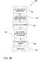
- FIG. 3Aillustrates one embodiment of a method 300 for packaging a semiconductor chip or die or other circuit element in a ball grid array package such as the package shown in FIGS. 2 A- 2 B.
- a step 302one or more semiconductor die are mounted in corresponding cavities of a container using, for example, a two part epoxy, a thermal epoxy, other thermally conductive adhesive, or solder. Substrates are attached to each of the semiconductor die and associated containers in step 306 . The semiconductor die are wire bonded to the substrates in a step 308 and solder bumps are formed on the substrates in a step 309 . Bond caps are formed in a step 310 . For fabrication of BGA assemblies from a container strip and a substrate strip, individual BGA assemblies are singulated from an assembled strip in a step 314 , and a perimeter seal applied in a step 316 .
- FIG. 3Billustrates an alternative method 350 .
- dieare attached to a substrate and in a step 352 , the die are wire bonded to a substrate.
- a containeris attached in a step 358 , and a wire bond slot is filled with an epoxy or other resin in a step 369 .
- a cavity formed by the container, the die, and the substrateis also partially or completely filled with an epoxy resin or other material.
- solder bumpsare attached and individual BGA assemblies are signulated.
- FIGS. 4 A- 4 BAlternative containers 401 - 405 are illustrated in FIGS. 4 A- 4 B.
- the container 401 of FIG. 4Aincludes a ridged region 411 formed by one or more die supports 413 that support a semiconductor die 414 .
- the ridges in this examplecomprise undulations in the base of the container.
- the die supports 413are situated so that a die surface 417 is approximately parallel and aligned with a plane defined by a container mounting surface 419 .
- the die supports 413are formed in a wall 425 (FIG. 4B) of the container 402 but in alternative arrangements, die supports can be formed of an additional layer of thermally conductive material, such as a copper foil, and attached to a container by, for example, spot welding or with a thermally conductive adhesive.
- the container 402 of FIG. 4Bincludes an array of die supports 423 .
- the die supports 423can be provided uniformly or concentrated at regions of the container 402 at which a die generates substantial heat.
- FIG. 4Cillustrates a container 405 that includes die supports 471 having spherical, elliptical, or otherwise curved die mounting surfaces 473 .
- FIG. 4Dillustrates a heat dissipating container 403 formed with machining operations in a copper strip or plate 432 (or strip or plate of other thermally conductive, heat absorbing, or heat dissipative material) that includes a cavity 434 configured to retain a semiconductor die 436 .
- Die supports 438are provided on a surface 440 of the cavity 434 .
- FIG. 4Eillustrates a container 404 that includes a heat sink 460 , shown in FIG. 4E as a series of grooves 462 and ridges 464 .
- the heat sink 460can, for example, be formed integrally with the container or can be provided as a separate piece and bonded to a container with a thermally conductive epoxy, welding, or other method.
- solder bumpsincludes solder balls and solder in any other projecting shape, and solder refers to an electrically conducting material that reflows when heated.
Landscapes
- Engineering & Computer Science (AREA)
- Microelectronics & Electronic Packaging (AREA)
- Computer Hardware Design (AREA)
- Power Engineering (AREA)
- Physics & Mathematics (AREA)
- Condensed Matter Physics & Semiconductors (AREA)
- General Physics & Mathematics (AREA)
- Manufacturing & Machinery (AREA)
- Chemical & Material Sciences (AREA)
- Materials Engineering (AREA)
- Cooling Or The Like Of Semiconductors Or Solid State Devices (AREA)
Abstract
Description
- The invention pertains to methods and apparatus for packaging electronic components such as semiconductor die.[0001]
- The miniaturization of electronic devices such as integrated circuits continues to drive the costs of electronic products down even as the performance of these products increases. The development of improved lithographic methods and other fabrication processes as well as improved packaging and circuit interconnection methods have been important factors this trend.[0002]
- While improvements in fabrication processes for miniaturization permit inexpensive manufacture of ever smaller devices, the interconnection of smaller devices can be difficult and expensive. In addition, the operation of smaller devices presents additional difficulties. Such smaller devices frequently are required to perform at least the same functions as the larger devices that they replace, and in many cases are expected to perform these functions faster and at a lower cost. A small device that operates at high speeds tends to generate large amounts of heat in a smaller volume, and dissipation of this heat is essential to avoid damage to the device so that the device has an acceptable time to failure. Therefore, improved circuit packages and packaging methods are needed that permit improved heat transfer.[0003]
- Another significant problem in the use of integrated circuits is packaging the integrated circuit in such a way as to electrically connect to many, densely spaced input/output electrical connections. If the input/output electrical connections must be spread out to permit electrical connections to other integrated circuits, other circuits or circuit components such as printed circuit boards, then much of the advantage of integrated circuit miniaturization is lost.[0004]
- One method of packaging integrated circuits for electrical connection to a printed circuit board is the so-called ball grid array (BGA) package. A BGA package includes a semiconductor die (an integrated circuit) that is attached to a substrate. Electrical connections are made from the die to the substrate with bond wires that are attached to bond pads provided on the die and the substrate. The bond pads on the substrate are electrically connected to an array of solder balls or bumps, and these solder balls are used to bond and make electrical connection to the printed circuit board. BGA packages are described in, for example, Tsuji et al., U.S. Pat. No. 5,930,603, Tsunoda et al., U.S. Pat. No. 5,914,531, and Tsuji et al., U.S. Pat. No. 5,293,072.[0005]
- Not only are BGA packages more compact than other packages, BGA packaged devices generally have superior thermal and electrical properties. The solder balls provide an excellent thermal path for the removal of heat from the semiconductor die as well as providing low resistance, low inductance electrical connections. Nevertheless, improved BGA packages that provide even denser interconnections and greater heat removal are needed.[0006]
- Containers for packaging semiconductor die are provided that include a thermally conductive strip having recesses configured to retain a semiconductor die. The containers may include at least one die standoff that extends into the recess. The die standoff is configured to provide a thermally conductive path between the semiconductor die and the container and fix the standoff distance. In representative embodiments, the thermally conductive material is a metal such as copper. In additional embodiments, the containers include a mounting surface for attaching the container to a substrate and the die standoff is configured so that a substrate attachment surface of the semiconductor die is substantially coplanar with the mounting surface with the die situated on the die standoff.[0007]
- Packaged semiconductor die are provided that include a thermally conductive container bonded to the semiconductor die and a substrate bonded to the container. The packaged semiconductor die also include at least one interconnect that electrically connects the semiconductor die to the substrate. In further embodiments, a first surface of the substrate is bonded to the container and at least one solder bump projects from a surface of the substrate opposite the first surface. In still further embodiments, the packaged semiconductor die include a perimeter seal that encapsulates at least a portion of a perimeter of the substrate and a bond cap that encapsulates the interconnect. In other embodiments, the packaged die include an encapsulant that fills a cavity defined by the semiconductor die and the container.[0008]
- Integrated circuit assemblies are provided that include a substrate and a semiconductor die electrically connected to the substrate. Solder bumps electrically connect the circuit board to the substrate, and the semiconductor die is attached to a thermally conductive container.[0009]
- Packages for semiconductor die are provided that include a thermally conductive container defining a recess configured to receive a semiconductor die. The packages include a heat sink attached to the container, and, in representative embodiments, the heat sink and the container are of a unitary one-piece integral construction.[0010]
- Methods of removing heat from a circuit assembly are provided that include providing a container of a thermally conducive material and attaching the semiconductor die to the container with a thermally conductive layer. A cavity defined by the semiconductor die and the container is filled with a thermally conductive encapsulant. In further embodiments, the semiconductor die and the container includes respective substrate mounting surfaces that are selected to be substantially coplanar.[0011]
- Methods of packaging a semiconductor die include providing a thermally conductive container that includes at least one die support and situating the die at least partially within the container. The die is secured to the container with a heat conductive layer such as a thermally conductive epoxy and the die support is thermally conductive.[0012]
- Methods of packaging include mounting a plurality of semiconductor die in corresponding cavities formed in a cavity strip; and attaching a substrate strip to the cavity strip. The plurality of die are separated by cutting the cavity strip and the substrate strip after attachment.[0013]
- These and other features and advantages of the invention are set forth below with reference to the accompanying drawings.[0014]
- FIGS.[0015]1A-1B are perspective views of an exemplary ball grid array package for a semiconductor die.
- FIG. 1C is a sectional view of the ball grid array package of FIGS.[0016]1A-1B.
- FIGS.[0017]2A-2B are a perspective view and a sectional view, respectively, illustrating an embodiment of BGA assemblies produced with a container strip and a substrate strip.
- FIG. 3 is a block diagram of a method of packaging semiconductor die in ball grid array package.[0018]
- FIGS.[0019]4A-4D are sectional views illustrating alternative containers for ball grid array packages.
- FIG. 4E is a perspective view of a form of BGA assembly that includes an array of die supports.[0020]
- With reference to FIGS.[0021]1A-1C, a ball grid array (“BGA”)
assembly 100 in one form includes asemiconductor die 102 that is partially enclosed by a thermallyconductive container 104 that attaches to asubstrate 106. The die102 is typically attached to adie mounting surface 107 of thesubstrate 106 with anadhesive layer 108. Thesubstrate 106 may be a multilayer material that includes layers of conducting and insulating materials. Representative materials include insulating circuit board base materials such as polyimide, glass epoxy, and glass fiber layers, as well as conducting layers such as copper, and solder resist layers. Theadhesive layer 108 may be a two part epoxy, a thermosetting epoxy, or other adhesive. - The[0022]
substrate 106 in this example includes a pattern layer110 (or several pattern layers) and thedie 102 is electrically connected to thepattern layer 110 withbond wires 114 that attach to bondpads 112 on thedie 102 and thesubstrate 106. Thebond wires 114 generally connect to thepattern layer 110 by extending through an aperture132 (referred to as a “wire bond slot”) in thesubstrate 106. Abond cap 134 of an epoxy resin, a cured liquid encapsulant, a molded plastic, or other material covers thebond wires 114 and fills theaperture 132, protecting thebond wires 114, thedie 102, and edges of thesubstrate 106. Solder bumps116 are situated atbond pads 117 provided on asoldering surface 118 of thesubstrate 106. Anencapsulant layer 138 seals to thebond cap 134 and covers or partially covers thebond cap 134. The solder bumps116 are generally soldered to thebond pads 117 and electrically connected to thepattern layer 110. The solder bumps116 are used in an additional soldering process or processes to electrically connect thedie 102 to a circuit board or other circuit assembly. - The[0023]
BGA assembly 100 of the form shown in FIGS.1A-1C includes amoisture barrier 120 that covers perimeter edges of thesubstrate 106 and thecontainer 104. The illustratedmoisture barrier 120 extends to cover anedge region 150 of thesubstrate 106 and thecontainer 104. In alternative embodiments, themoisture barrier 120 is omitted or extends to cover only selected portions of theedge region 150. Referring to FIG. 1C, thedie 102 is thermally connected to diesupports 122 formed in thecontainer 104. The die supports122 contact or closely approach thedie 102 to increase thermal conductance from thedie 102 to thecontainer 104. Thecontainer 104 and the die supports122 are conveniently formed of a single piece of a thermally conductive material such as copper strip or copper foil, or other heat dissipating or heat absorbing material. Alternatively, thesupports 122 can be fabricated separately and then attached to thecontainer 104. The die supports122 may be configured so that a die attachsurface 124 of thedie 102 is substantially coplanar with asurface 126 of thecontainer 104 with thedie 102 in contact with thesupports 122. As used herein, thesurfaces layers die 102 is generally attached to thecontainer 104 such as with a thermally conductive epoxy or other adhesive that substantially fills acavity 130 defined by thedie 102 and thecontainer 104. A thermally conductive epoxy, other adhesive, or resin may be used to fill avolume 131 defined by thesubstrate 106 and thecontainer 104 at a perimeter of thedie 102. Theencapsulant layer 138 covers thebond cap 132 and portions of asurface 140 of thesubstrate 106. - The semiconductor die[0024]102 and the
bond wires 106 in the embodiment of FIGS.1A-1C are encapsulated by abond cap 134 that can be made of a cured liquid encapsulant, a cured epoxy, a molded plastic, a cured liquid resin, or other material. In addition, while thecontainer 104 includes diestandoffs 122, containers without die standoffs can be provided. - BGA assemblies such as the[0025]
BGA assembly 100 of FIGS.1A-1D may also be produced in the form of aBGA assembly strip 200, as illustrated in FIGS.2A-2B. Semiconductor die201a-201dare mounted (e.g., adhesively bonded with a thermally conductive adhesive) in respective cavities203a-203dof containers204a-204dof acontainer strip 205. The semiconductor die201a-201dgenerally contact die supports207 provided at each of the cavities203a-203d.Asubstrate strip 209 includes substrates210a-210dthat are connected with thebars 211. Thesubstrate strip 209 is attached to the semiconductor die201a-201dand thecontainer strip 205, such as generally with a layer of an adhesive. Thesubstrate strip 209 is aligned with respect to thecontainer strip 205 so thatbond wires 212 pass through apertures214a-214dand electrically connect the semiconductor die201a-201dto respective substrates210a-210d. FIGS.2A-2B show four semiconductor die201a-201dattached to thecontainer strip 205, but longer or shorter container strips and substrate strips can be used to mount more or fewer semiconductor die. After the semiconductor die201a-201dare attached and wire bonded to thecontainer strip 205 and thesubstrate strip 209, solder bumps (not shown) may be formed on thesubstrate strip 209 in a conventional manner. Thesubstrate strip 209 andcontainer strip 205 are then cut, sheared, or routed at the tie bars211 alongcut lines 220 so that the semiconductor die201a-201dare attached to respective substrates210a-210dand containers204a-204dand are available as individual BGA assemblies. - FIG. 3A illustrates one embodiment of a[0026]
method 300 for packaging a semiconductor chip or die or other circuit element in a ball grid array package such as the package shown in FIGS.2A-2B. In astep 302, one or more semiconductor die are mounted in corresponding cavities of a container using, for example, a two part epoxy, a thermal epoxy, other thermally conductive adhesive, or solder. Substrates are attached to each of the semiconductor die and associated containers instep 306. The semiconductor die are wire bonded to the substrates in astep 308 and solder bumps are formed on the substrates in astep 309. Bond caps are formed in astep 310. For fabrication of BGA assemblies from a container strip and a substrate strip, individual BGA assemblies are singulated from an assembled strip in astep 314, and a perimeter seal applied in astep 316. - FIG. 3B illustrates an[0027]
alternative method 350. In astep 352, die are attached to a substrate and in astep 352, the die are wire bonded to a substrate. A container is attached in astep 358, and a wire bond slot is filled with an epoxy or other resin in a step369. In the step369, a cavity formed by the container, the die, and the substrate is also partially or completely filled with an epoxy resin or other material. Insteps - Alternative containers[0028]401-405 are illustrated in FIGS.4A-4B. The
container 401 of FIG. 4A includes a ridgedregion 411 formed by one or more die supports413 that support a semiconductor die414. The ridges in this example comprise undulations in the base of the container. The die supports413 are situated so that adie surface 417 is approximately parallel and aligned with a plane defined by acontainer mounting surface 419. The die supports413 are formed in a wall425 (FIG. 4B) of thecontainer 402 but in alternative arrangements, die supports can be formed of an additional layer of thermally conductive material, such as a copper foil, and attached to a container by, for example, spot welding or with a thermally conductive adhesive. - The[0029]
container 402 of FIG. 4B includes an array of die supports423. The die supports423 can be provided uniformly or concentrated at regions of thecontainer 402 at which a die generates substantial heat. FIG. 4C illustrates acontainer 405 that includes diesupports 471 having spherical, elliptical, or otherwise curveddie mounting surfaces 473. - Containers of a foil or other ductile material can be formed by pressing with or into a mold. Other methods of fabrication include machining and etching. FIG. 4D illustrates a[0030]
heat dissipating container 403 formed with machining operations in a copper strip or plate432 (or strip or plate of other thermally conductive, heat absorbing, or heat dissipative material) that includes acavity 434 configured to retain asemiconductor die 436. Die supports438 are provided on asurface 440 of thecavity 434. Thecavity 434 is configured to at least partially enclose the semiconductor die436, and the die supports438 are conveniently configured so that abonding surface 456 of thedie 436 is substantially coplanar with asurface 458 of thecontainer 403. FIG. 4E illustrates acontainer 404 that includes aheat sink 460, shown in FIG. 4E as a series ofgrooves 462 andridges 464. Theheat sink 460 can, for example, be formed integrally with the container or can be provided as a separate piece and bonded to a container with a thermally conductive epoxy, welding, or other method. - While the example BGA assemblies described above include solder balls, solder bumps or other solder shapes can be used. As used herein, solder bumps includes solder balls and solder in any other projecting shape, and solder refers to an electrically conducting material that reflows when heated.[0031]
- While the invention is described with respect to particular implementations, the invention is not limited to these implementations. The invention is directed to novel and non-obvious aspects of this disclosure, both individually and in combination as set forth in the claims below.[0032]
Claims (30)
Priority Applications (1)
| Application Number | Priority Date | Filing Date | Title |
|---|---|---|---|
| US10/209,753US7399657B2 (en) | 2000-08-31 | 2002-07-31 | Ball grid array packages with thermally conductive containers |
Applications Claiming Priority (2)
| Application Number | Priority Date | Filing Date | Title |
|---|---|---|---|
| US09/653,127US6559537B1 (en) | 2000-08-31 | 2000-08-31 | Ball grid array packages with thermally conductive containers |
| US10/209,753US7399657B2 (en) | 2000-08-31 | 2002-07-31 | Ball grid array packages with thermally conductive containers |
Related Parent Applications (1)
| Application Number | Title | Priority Date | Filing Date |
|---|---|---|---|
| US09/653,127DivisionUS6559537B1 (en) | 2000-08-31 | 2000-08-31 | Ball grid array packages with thermally conductive containers |
Publications (2)
| Publication Number | Publication Date |
|---|---|
| US20020187590A1true US20020187590A1 (en) | 2002-12-12 |
| US7399657B2 US7399657B2 (en) | 2008-07-15 |
Family
ID=24619586
Family Applications (2)
| Application Number | Title | Priority Date | Filing Date |
|---|---|---|---|
| US09/653,127Expired - LifetimeUS6559537B1 (en) | 2000-08-31 | 2000-08-31 | Ball grid array packages with thermally conductive containers |
| US10/209,753Expired - LifetimeUS7399657B2 (en) | 2000-08-31 | 2002-07-31 | Ball grid array packages with thermally conductive containers |
Family Applications Before (1)
| Application Number | Title | Priority Date | Filing Date |
|---|---|---|---|
| US09/653,127Expired - LifetimeUS6559537B1 (en) | 2000-08-31 | 2000-08-31 | Ball grid array packages with thermally conductive containers |
Country Status (1)
| Country | Link |
|---|---|
| US (2) | US6559537B1 (en) |
Cited By (9)
| Publication number | Priority date | Publication date | Assignee | Title |
|---|---|---|---|---|
| US20060087037A1 (en)* | 2004-10-22 | 2006-04-27 | Phoenix Precision Technology Corporation | Substrate structure with embedded chip of semiconductor package and method for fabricating the same |
| US20060237845A1 (en)* | 2002-04-15 | 2006-10-26 | Micron Technology, Inc. | Semiconductor integrated circuit package having electrically disconnected solder balls for mounting |
| DE102007002156A1 (en)* | 2007-01-15 | 2008-07-17 | Infineon Technologies Ag | Semiconductor arrangement, comprises heat sink body, which is provided for dissipating heat from semiconductor component, where heat sink has electric conductive body with recess for receiving semiconductor component |
| US20160157334A1 (en)* | 2013-05-22 | 2016-06-02 | Kaneka Corporation | Heat dissipating structure |
| US10332814B2 (en) | 2015-02-23 | 2019-06-25 | Infineon Technologies Ag | Bonded system and a method for adhesively bonding a hygroscopic material |
| US10575437B1 (en) | 2019-03-20 | 2020-02-25 | Northrop Grumman Systems Corporation | Temperature control method, system, and apparatus |
| US10595441B1 (en)* | 2019-04-03 | 2020-03-17 | Northrop Grumman Systems Corporation | Method and apparatus for separating a thermal load path from a structural load path in a circuit board environment |
| US10645845B2 (en) | 2018-04-12 | 2020-05-05 | Northrop Grumman Systems Corporation | Forced flow cooling temperature control method, system, and apparatus |
| US10782258B2 (en) | 2018-09-04 | 2020-09-22 | Northrop Grumman Systems Corporation | Superconductor critical temperature measurement |
Families Citing this family (10)
| Publication number | Priority date | Publication date | Assignee | Title |
|---|---|---|---|---|
| US6963142B2 (en) | 2001-10-26 | 2005-11-08 | Micron Technology, Inc. | Flip chip integrated package mount support |
| TWI237356B (en)* | 2002-11-04 | 2005-08-01 | Siliconware Precision Industries Co Ltd | Tray for ball grid array semiconductor packages |
| US7153725B2 (en)* | 2004-01-27 | 2006-12-26 | St Assembly Test Services Ltd. | Strip-fabricated flip chip in package and flip chip in system heat spreader assemblies and fabrication methods therefor |
| US7851268B2 (en)* | 2005-04-09 | 2010-12-14 | Stats Chippac Ltd. | Integrated circuit package system using heat slug |
| TW201032293A (en)* | 2009-02-23 | 2010-09-01 | Etron Technology Inc | Moisture-proof device, moisture-proof chip, and method for increasing moisture-proof capability of chip |
| US8205766B2 (en)* | 2009-05-20 | 2012-06-26 | The Bergquist Company | Method for packaging thermal interface materials |
| US20110048786A1 (en)* | 2009-08-31 | 2011-03-03 | Samsung Electro-Mechanics Co., Ltd. | Printed circuit board having a bump and a method of manufacturing the same |
| US8541886B2 (en)* | 2010-03-09 | 2013-09-24 | Stats Chippac Ltd. | Integrated circuit packaging system with via and method of manufacture thereof |
| US9064881B2 (en)* | 2010-11-11 | 2015-06-23 | Taiwan Semiconductor Manufacturing Company, Ltd. | Protecting flip-chip package using pre-applied fillet |
| US9099514B2 (en)* | 2012-03-21 | 2015-08-04 | Taiwan Semiconductor Manufacturing Company, Ltd. | Wafer holder with tapered region |
Citations (97)
| Publication number | Priority date | Publication date | Assignee | Title |
|---|---|---|---|---|
| US2570221A (en)* | 1948-02-20 | 1951-10-09 | Int Standard Electric Corp | Pulse code modulation system |
| US4012768A (en)* | 1975-02-03 | 1977-03-15 | Motorola, Inc. | Semiconductor package |
| US4312116A (en)* | 1980-04-14 | 1982-01-26 | International Business Machines Corporation | Method of sealing an electronic module in a cap |
| US4514752A (en)* | 1984-04-10 | 1985-04-30 | International Business Machines Corporation | Displacement compensating module |
| US4563725A (en)* | 1983-01-06 | 1986-01-07 | Welwyn Electronics Limited | Electrical assembly |
| US4641176A (en)* | 1981-01-26 | 1987-02-03 | Burroughs Corporation | Semiconductor package with contact springs |
| US5139972A (en)* | 1991-02-28 | 1992-08-18 | General Electric Company | Batch assembly of high density hermetic packages for power semiconductor chips |
| US5157478A (en)* | 1989-04-19 | 1992-10-20 | Mitsubishi Denki Kabushiki Kaisha | Tape automated bonding packaged semiconductor device incorporating a heat sink |
| US5163551A (en)* | 1991-06-28 | 1992-11-17 | Digital Equipment Corporation | Integrated circuit device carrier |
| US5199564A (en)* | 1992-03-13 | 1993-04-06 | Minnesota Mining And Manufacturing Company | Carrier tape for electronic through-hole components |
| US5216278A (en)* | 1990-12-04 | 1993-06-01 | Motorola, Inc. | Semiconductor device having a pad array carrier package |
| US5220486A (en)* | 1990-09-14 | 1993-06-15 | Kabushiki Kaisha Toshiba | Ic packing device |
| US5223739A (en)* | 1989-09-14 | 1993-06-29 | Kabushiki Kaisha Toshiba | Plastic molded semiconductor device having waterproof cap |
| US5246129A (en)* | 1992-03-13 | 1993-09-21 | Illinois Tool Works, Inc. | Shipping tray and cover strip |
| US5279029A (en)* | 1990-08-01 | 1994-01-18 | Staktek Corporation | Ultra high density integrated circuit packages method |
| US5293072A (en)* | 1990-06-25 | 1994-03-08 | Fujitsu Limited | Semiconductor device having spherical terminals attached to the lead frame embedded within the package body |
| US5311060A (en)* | 1989-12-19 | 1994-05-10 | Lsi Logic Corporation | Heat sink for semiconductor device assembly |
| US5343076A (en)* | 1990-07-21 | 1994-08-30 | Mitsui Petrochemical Industries, Ltd. | Semiconductor device with an airtight space formed internally within a hollow package |
| US5362679A (en)* | 1993-07-26 | 1994-11-08 | Vlsi Packaging Corporation | Plastic package with solder grid array |
| US5365107A (en)* | 1992-06-04 | 1994-11-15 | Shinko Electric Industries, Co., Ltd. | Semiconductor device having tab tape |
| US5416357A (en)* | 1991-12-17 | 1995-05-16 | Rohm Co., Ltd. | Semiconductor integrated circuit device |
| US5422231A (en)* | 1993-03-05 | 1995-06-06 | Fuji Photo Film Co., Ltd. | Photographic product |
| US5440169A (en)* | 1993-01-08 | 1995-08-08 | Mitsubishi Denki Kabushiki Kaisha | Resin-packaged semiconductor device with flow prevention dimples |
| US5448114A (en)* | 1992-07-15 | 1995-09-05 | Kabushiki Kaisha Toshiba | Semiconductor flipchip packaging having a perimeter wall |
| US5524765A (en)* | 1994-11-15 | 1996-06-11 | Tempo G | Carrier tape packaging system utilizing a layer of gel for retaining small components |
| US5557150A (en)* | 1992-02-07 | 1996-09-17 | Lsi Logic Corporation | Overmolded semiconductor package |
| US5594204A (en)* | 1995-03-20 | 1997-01-14 | National Semiconductor Corporation | Overmolded PC board with ESD protection and EMI suppression |
| US5604376A (en)* | 1994-06-30 | 1997-02-18 | Digital Equipment Corporation | Paddleless molded plastic semiconductor chip package |
| US5625222A (en)* | 1993-11-18 | 1997-04-29 | Fujitsu Limited | Semiconductor device in a resin package housed in a frame having high thermal conductivity |
| US5650593A (en)* | 1994-05-26 | 1997-07-22 | Amkor Electronics, Inc. | Thermally enhanced chip carrier package |
| US5653020A (en)* | 1994-09-30 | 1997-08-05 | Sgs-Thomson Microelectronics, S.R.L. | Method for forming plastic packages, in particular thin packages, for semiconductor electronic devices |
| US5667073A (en)* | 1994-06-23 | 1997-09-16 | Okui; Tokujiro | Carrier tape for storage use of electronic components |
| US5677566A (en)* | 1995-05-08 | 1997-10-14 | Micron Technology, Inc. | Semiconductor chip package |
| US5708304A (en)* | 1996-03-27 | 1998-01-13 | Mitsubishi Denki Kabushiki Kaisha | Semiconductor device |
| US5710459A (en)* | 1995-05-12 | 1998-01-20 | Industrial Technology Research Institute | Integrated circuit package provided with multiple heat-conducting paths for enhancing heat dissipation and wrapping around cap for improving integrity and reliability |
| US5729963A (en)* | 1995-07-11 | 1998-03-24 | Minnesota Mining And Manufacturing Company | Component carrier tape |
| US5766972A (en)* | 1994-06-02 | 1998-06-16 | Mitsubishi Denki Kabushiki Kaisha | Method of making resin encapsulated semiconductor device with bump electrodes |
| US5770479A (en)* | 1996-01-11 | 1998-06-23 | Micron Technology, Inc. | Bonding support for leads-over-chip process |
| US5775510A (en)* | 1995-01-04 | 1998-07-07 | Micron Technology, Inc. | UV light sensitive die-pac for securing semiconductor dice during transport |
| US5796162A (en)* | 1996-09-17 | 1998-08-18 | Greatek Technology Co., Ltd. | Frames locking method for packaging semiconductor chip |
| US5811879A (en)* | 1996-06-26 | 1998-09-22 | Micron Technology, Inc. | Stacked leads-over-chip multi-chip module |
| US5819398A (en)* | 1995-07-31 | 1998-10-13 | Sgs-Thomson Microelectronics, Ltd. | Method of manufacturing a ball grid array package |
| US5869889A (en)* | 1997-04-21 | 1999-02-09 | Lsi Logic Corporation | Thin power tape ball grid array package |
| US5880933A (en)* | 1997-08-18 | 1999-03-09 | Daimlerchrysler Corporation | Heat sinking module cover |
| US5893724A (en)* | 1995-10-28 | 1999-04-13 | Institute Of Microelectronics | Method for forming a highly reliable and planar ball grid array package |
| US5895967A (en)* | 1997-07-07 | 1999-04-20 | Texas Instruments Incorporated | Ball grid array package having a deformable metal layer and method |
| US5909056A (en)* | 1997-06-03 | 1999-06-01 | Lsi Logic Corporation | High performance heat spreader for flip chip packages |
| US5914531A (en)* | 1994-02-10 | 1999-06-22 | Hitachi, Ltd. | Semiconductor device having a ball grid array package structure using a supporting frame |
| US5930603A (en)* | 1996-12-02 | 1999-07-27 | Fujitsu Limited | Method for producing a semiconductor device |
| US5960961A (en)* | 1998-08-03 | 1999-10-05 | Tempo G | Tab means to assure ready release of singulated wafer die or integrated circuit chips packed in adhesive backed carrier tapes |
| US5976912A (en)* | 1994-03-18 | 1999-11-02 | Hitachi Chemical Company, Ltd. | Fabrication process of semiconductor package and semiconductor package |
| US5986340A (en)* | 1996-05-02 | 1999-11-16 | National Semiconductor Corporation | Ball grid array package with enhanced thermal and electrical characteristics and electronic device incorporating same |
| US5990544A (en)* | 1997-07-07 | 1999-11-23 | Nippon Steel Semiconductor Corp. | Lead frame and a semiconductor device having the same |
| US6023098A (en)* | 1995-06-29 | 2000-02-08 | Fujitsu Limited | Semiconductor device having terminals for heat radiation |
| US6032355A (en)* | 1998-04-22 | 2000-03-07 | World Wiser Electronics, Inc. | Method of forming thermal conductive structure on printed circuit board |
| US6032362A (en)* | 1996-08-09 | 2000-03-07 | Hitachi Metals, Ltd. | Method for producing a heat spreader and semiconductor device with a heat spreader |
| US6038136A (en)* | 1997-10-29 | 2000-03-14 | Hestia Technologies, Inc. | Chip package with molded underfill |
| US6049038A (en)* | 1997-08-01 | 2000-04-11 | Nec Corporation | Flip-chip resin sealing structure and resin sealing method |
| US6075288A (en)* | 1998-06-08 | 2000-06-13 | Micron Technology, Inc. | Semiconductor package having interlocking heat sinks and method of fabrication |
| US6075289A (en)* | 1996-10-24 | 2000-06-13 | Tessera, Inc. | Thermally enhanced packaged semiconductor assemblies |
| US6080932A (en)* | 1998-04-14 | 2000-06-27 | Tessera, Inc. | Semiconductor package assemblies with moisture vents |
| US6097609A (en)* | 1998-12-30 | 2000-08-01 | Intel Corporation | Direct BGA socket |
| US6114189A (en)* | 1997-09-10 | 2000-09-05 | Lsi Logic Corp. | Molded array integrated circuit package |
| US6122171A (en)* | 1999-07-30 | 2000-09-19 | Micron Technology, Inc. | Heat sink chip package and method of making |
| US6149010A (en)* | 1998-10-12 | 2000-11-21 | Fujitsu Takamisa Component Limited | Carrier for electronic parts |
| US6175497B1 (en)* | 1998-09-30 | 2001-01-16 | World Wiser Electronics Inc. | Thermal vias-provided cavity-down IC package structure |
| US6179127B1 (en)* | 1996-10-18 | 2001-01-30 | Shin-Etsu Polymer Co., Ltd. | Carrier tape and die apparatus for forming same |
| US6187612B1 (en)* | 1998-02-17 | 2001-02-13 | Texas Instruments Incorporated | Molded ball grid array package mold die |
| US6225144B1 (en)* | 1999-03-01 | 2001-05-01 | Motorola, Inc. | Method and machine for underfilling an assembly to form a semiconductor package |
| US6249403B1 (en)* | 1997-05-23 | 2001-06-19 | Hitachi, Ltd. | Magnetic hard disk drive and process for producing the same |
| US6258630B1 (en)* | 1999-02-04 | 2001-07-10 | Nec Corporation | Resin-sealed semiconductor device having island for mounting semiconductor element coupled to heat spreader |
| US6261870B1 (en)* | 1998-08-28 | 2001-07-17 | Lsi Logic Corporation | Backside failure analysis capable integrated circuit packaging |
| US6271058B1 (en)* | 1998-01-06 | 2001-08-07 | Nec Corporation | Method of manufacturing semiconductor device in which semiconductor chip is mounted facedown on board |
| US6300165B2 (en)* | 1999-11-15 | 2001-10-09 | Substrate Technologies Incorporated | Ball grid substrate for lead-on-chip semiconductor package |
| US20010040288A1 (en)* | 1999-07-28 | 2001-11-15 | Hironori Matsushima | Packaged semiconductor device and manufacturing method thereof |
| US6351030B2 (en)* | 1997-09-29 | 2002-02-26 | International Business Machines Corporation | Electronic package utilizing protective coating |
| US6357594B1 (en)* | 1998-06-30 | 2002-03-19 | Tempo G | Means to assure ready release of singulated wafer die or integrated circuit chips packed in adhesive backed carrier tapes |
| US6362530B1 (en)* | 1998-04-06 | 2002-03-26 | National Semiconductor Corporation | Manufacturing methods and construction for integrated circuit packages |
| US6376907B1 (en)* | 1997-12-01 | 2002-04-23 | Kabushiki Kaisha Toshiba | Ball grid array type package for semiconductor device |
| US20020060369A1 (en)* | 1999-09-02 | 2002-05-23 | Salman Akram | Board-on-chip packages with conductive foil on the chip surface |
| US6395124B1 (en)* | 1999-07-30 | 2002-05-28 | 3M Innovative Properties Company | Method of producing a laminated structure |
| US6404070B1 (en)* | 1999-08-03 | 2002-06-11 | Shinko Electric Industries Co., Ltd. | Semiconductor device |
| US6425484B1 (en)* | 1997-09-10 | 2002-07-30 | Yayoi Corporation | Tape-shaped parts package, parts storing tape, tape-shaped cover and parts packaging apparatus |
| US6429530B1 (en)* | 1998-11-02 | 2002-08-06 | International Business Machines Corporation | Miniaturized chip scale ball grid array semiconductor package |
| US6432749B1 (en)* | 1999-08-24 | 2002-08-13 | Texas Instruments Incorporated | Method of fabricating flip chip IC packages with heat spreaders in strip format |
| US6432742B1 (en)* | 2000-08-17 | 2002-08-13 | St Assembly Test Services Pte Ltd. | Methods of forming drop-in heat spreader plastic ball grid array (PBGA) packages |
| US6440599B1 (en)* | 1997-04-21 | 2002-08-27 | Toyo Kohan Co., Ltd. | Hermetically sealed cell |
| US6486554B2 (en)* | 2001-03-30 | 2002-11-26 | International Business Machines Corporation | Molded body for PBGA and chip-scale packages |
| US6541310B1 (en)* | 2000-07-24 | 2003-04-01 | Siliconware Precision Industries Co., Ltd. | Method of fabricating a thin and fine ball-grid array package with embedded heat spreader |
| US6568535B1 (en)* | 2000-01-14 | 2003-05-27 | Peak International Ltd. | Apparatus and methods for improving uniform cover tape adhesion on a carrier tape |
| US6576988B2 (en)* | 1999-08-30 | 2003-06-10 | Micron Technology, Inc. | Semiconductor package |
| US6579399B1 (en)* | 1998-10-28 | 2003-06-17 | Micron Technology Inc | Method and system for handling semiconductor components |
| US6586845B1 (en)* | 1998-10-28 | 2003-07-01 | Shinko Electric Industries Co., Ltd. | Semiconductor device module and a part thereof |
| US6626656B2 (en)* | 1998-02-05 | 2003-09-30 | Micron Technology, Inc. | Apparatus for encasing array packages |
| US6644982B1 (en)* | 1998-12-04 | 2003-11-11 | Formfactor, Inc. | Method and apparatus for the transport and tracking of an electronic component |
| US6650005B2 (en)* | 2001-06-13 | 2003-11-18 | Walsin Advanced Electronics Ltd | Micro BGA package |
| US6653730B2 (en)* | 2000-12-14 | 2003-11-25 | Intel Corporation | Electronic assembly with high capacity thermal interface |
Family Cites Families (17)
| Publication number | Priority date | Publication date | Assignee | Title |
|---|---|---|---|---|
| JPS58122753A (en)* | 1982-01-14 | 1983-07-21 | Nec Corp | High density chip carrier |
| JPS59188948A (en)* | 1983-04-11 | 1984-10-26 | Nec Corp | Chip carrier |
| JPH01298753A (en)* | 1988-05-27 | 1989-12-01 | Nec Corp | Pin grid array integrated circuit package with heat sink |
| GB8825154D0 (en)* | 1988-10-27 | 1988-11-30 | Reel Service Ltd | Tape for storage of electronic components |
| JPH03116949A (en)* | 1989-09-29 | 1991-05-17 | Enplas Corp | Manufacture of ic package and ic package case |
| JPH0756890B2 (en)* | 1989-11-01 | 1995-06-14 | 株式会社後藤製作所 | Method for manufacturing semiconductor device |
| US5583377A (en)* | 1992-07-15 | 1996-12-10 | Motorola, Inc. | Pad array semiconductor device having a heat sink with die receiving cavity |
| JPH06275759A (en)* | 1993-03-17 | 1994-09-30 | Fujitsu Ltd | Semiconductor device and its manufacture |
| JP3161142B2 (en)* | 1993-03-26 | 2001-04-25 | ソニー株式会社 | Semiconductor device |
| US5583378A (en) | 1994-05-16 | 1996-12-10 | Amkor Electronics, Inc. | Ball grid array integrated circuit package with thermal conductor |
| US6166434A (en)* | 1997-09-23 | 2000-12-26 | Lsi Logic Corporation | Die clip assembly for semiconductor package |
| US6002178A (en) | 1997-11-12 | 1999-12-14 | Lin; Paul T. | Multiple chip module configuration to simplify testing process and reuse of known-good chip-size package (CSP) |
| JP3087709B2 (en)* | 1997-12-08 | 2000-09-11 | 日本電気株式会社 | Semiconductor device and manufacturing method thereof |
| JP2000156435A (en) | 1998-06-22 | 2000-06-06 | Fujitsu Ltd | Semiconductor device and manufacturing method thereof |
| US6166435A (en)* | 1998-12-10 | 2000-12-26 | Industrial Technology Research Institute | Flip-chip ball grid array package with a heat slug |
| US6329220B1 (en) | 1999-11-23 | 2001-12-11 | Micron Technology, Inc. | Packages for semiconductor die |
| US6331453B1 (en) | 1999-12-16 | 2001-12-18 | Micron Technology, Inc. | Method for fabricating semiconductor packages using mold tooling fixture with flash control cavities |
- 2000
- 2000-08-31USUS09/653,127patent/US6559537B1/ennot_activeExpired - Lifetime
- 2002
- 2002-07-31USUS10/209,753patent/US7399657B2/ennot_activeExpired - Lifetime
Patent Citations (99)
| Publication number | Priority date | Publication date | Assignee | Title |
|---|---|---|---|---|
| US2570221A (en)* | 1948-02-20 | 1951-10-09 | Int Standard Electric Corp | Pulse code modulation system |
| US4012768A (en)* | 1975-02-03 | 1977-03-15 | Motorola, Inc. | Semiconductor package |
| US4312116A (en)* | 1980-04-14 | 1982-01-26 | International Business Machines Corporation | Method of sealing an electronic module in a cap |
| US4641176A (en)* | 1981-01-26 | 1987-02-03 | Burroughs Corporation | Semiconductor package with contact springs |
| US4563725A (en)* | 1983-01-06 | 1986-01-07 | Welwyn Electronics Limited | Electrical assembly |
| US4514752A (en)* | 1984-04-10 | 1985-04-30 | International Business Machines Corporation | Displacement compensating module |
| US5157478A (en)* | 1989-04-19 | 1992-10-20 | Mitsubishi Denki Kabushiki Kaisha | Tape automated bonding packaged semiconductor device incorporating a heat sink |
| US5223739A (en)* | 1989-09-14 | 1993-06-29 | Kabushiki Kaisha Toshiba | Plastic molded semiconductor device having waterproof cap |
| US5311060A (en)* | 1989-12-19 | 1994-05-10 | Lsi Logic Corporation | Heat sink for semiconductor device assembly |
| US5293072A (en)* | 1990-06-25 | 1994-03-08 | Fujitsu Limited | Semiconductor device having spherical terminals attached to the lead frame embedded within the package body |
| US6048754A (en)* | 1990-07-21 | 2000-04-11 | Mitsui Chemicals, Inc. | Method of manufacturing a semiconductor device with an airtight space formed internally within a hollow package |
| US5343076A (en)* | 1990-07-21 | 1994-08-30 | Mitsui Petrochemical Industries, Ltd. | Semiconductor device with an airtight space formed internally within a hollow package |
| US5279029A (en)* | 1990-08-01 | 1994-01-18 | Staktek Corporation | Ultra high density integrated circuit packages method |
| US5220486A (en)* | 1990-09-14 | 1993-06-15 | Kabushiki Kaisha Toshiba | Ic packing device |
| US5216278A (en)* | 1990-12-04 | 1993-06-01 | Motorola, Inc. | Semiconductor device having a pad array carrier package |
| US5139972A (en)* | 1991-02-28 | 1992-08-18 | General Electric Company | Batch assembly of high density hermetic packages for power semiconductor chips |
| US5163551A (en)* | 1991-06-28 | 1992-11-17 | Digital Equipment Corporation | Integrated circuit device carrier |
| US5416357A (en)* | 1991-12-17 | 1995-05-16 | Rohm Co., Ltd. | Semiconductor integrated circuit device |
| US5557150A (en)* | 1992-02-07 | 1996-09-17 | Lsi Logic Corporation | Overmolded semiconductor package |
| US5199564A (en)* | 1992-03-13 | 1993-04-06 | Minnesota Mining And Manufacturing Company | Carrier tape for electronic through-hole components |
| US5246129A (en)* | 1992-03-13 | 1993-09-21 | Illinois Tool Works, Inc. | Shipping tray and cover strip |
| US5365107A (en)* | 1992-06-04 | 1994-11-15 | Shinko Electric Industries, Co., Ltd. | Semiconductor device having tab tape |
| US5448114A (en)* | 1992-07-15 | 1995-09-05 | Kabushiki Kaisha Toshiba | Semiconductor flipchip packaging having a perimeter wall |
| US5440169A (en)* | 1993-01-08 | 1995-08-08 | Mitsubishi Denki Kabushiki Kaisha | Resin-packaged semiconductor device with flow prevention dimples |
| US5422231A (en)* | 1993-03-05 | 1995-06-06 | Fuji Photo Film Co., Ltd. | Photographic product |
| US5362679A (en)* | 1993-07-26 | 1994-11-08 | Vlsi Packaging Corporation | Plastic package with solder grid array |
| US5625222A (en)* | 1993-11-18 | 1997-04-29 | Fujitsu Limited | Semiconductor device in a resin package housed in a frame having high thermal conductivity |
| US5914531A (en)* | 1994-02-10 | 1999-06-22 | Hitachi, Ltd. | Semiconductor device having a ball grid array package structure using a supporting frame |
| US6114192A (en)* | 1994-02-10 | 2000-09-05 | Hitachi, Ltd. | Method of manufacturing a semiconductor device having a ball grid array package structure using a supporting frame |
| US5976912A (en)* | 1994-03-18 | 1999-11-02 | Hitachi Chemical Company, Ltd. | Fabrication process of semiconductor package and semiconductor package |
| US5650593A (en)* | 1994-05-26 | 1997-07-22 | Amkor Electronics, Inc. | Thermally enhanced chip carrier package |
| US5766972A (en)* | 1994-06-02 | 1998-06-16 | Mitsubishi Denki Kabushiki Kaisha | Method of making resin encapsulated semiconductor device with bump electrodes |
| US5667073A (en)* | 1994-06-23 | 1997-09-16 | Okui; Tokujiro | Carrier tape for storage use of electronic components |
| US5604376A (en)* | 1994-06-30 | 1997-02-18 | Digital Equipment Corporation | Paddleless molded plastic semiconductor chip package |
| US5653020A (en)* | 1994-09-30 | 1997-08-05 | Sgs-Thomson Microelectronics, S.R.L. | Method for forming plastic packages, in particular thin packages, for semiconductor electronic devices |
| US5524765A (en)* | 1994-11-15 | 1996-06-11 | Tempo G | Carrier tape packaging system utilizing a layer of gel for retaining small components |
| US5775510A (en)* | 1995-01-04 | 1998-07-07 | Micron Technology, Inc. | UV light sensitive die-pac for securing semiconductor dice during transport |
| US5594204A (en)* | 1995-03-20 | 1997-01-14 | National Semiconductor Corporation | Overmolded PC board with ESD protection and EMI suppression |
| US5677566A (en)* | 1995-05-08 | 1997-10-14 | Micron Technology, Inc. | Semiconductor chip package |
| US5710459A (en)* | 1995-05-12 | 1998-01-20 | Industrial Technology Research Institute | Integrated circuit package provided with multiple heat-conducting paths for enhancing heat dissipation and wrapping around cap for improving integrity and reliability |
| US6023098A (en)* | 1995-06-29 | 2000-02-08 | Fujitsu Limited | Semiconductor device having terminals for heat radiation |
| US5729963A (en)* | 1995-07-11 | 1998-03-24 | Minnesota Mining And Manufacturing Company | Component carrier tape |
| US5819398A (en)* | 1995-07-31 | 1998-10-13 | Sgs-Thomson Microelectronics, Ltd. | Method of manufacturing a ball grid array package |
| US5893724A (en)* | 1995-10-28 | 1999-04-13 | Institute Of Microelectronics | Method for forming a highly reliable and planar ball grid array package |
| US5770479A (en)* | 1996-01-11 | 1998-06-23 | Micron Technology, Inc. | Bonding support for leads-over-chip process |
| US5708304A (en)* | 1996-03-27 | 1998-01-13 | Mitsubishi Denki Kabushiki Kaisha | Semiconductor device |
| US5986340A (en)* | 1996-05-02 | 1999-11-16 | National Semiconductor Corporation | Ball grid array package with enhanced thermal and electrical characteristics and electronic device incorporating same |
| US5811879A (en)* | 1996-06-26 | 1998-09-22 | Micron Technology, Inc. | Stacked leads-over-chip multi-chip module |
| US6032362A (en)* | 1996-08-09 | 2000-03-07 | Hitachi Metals, Ltd. | Method for producing a heat spreader and semiconductor device with a heat spreader |
| US5796162A (en)* | 1996-09-17 | 1998-08-18 | Greatek Technology Co., Ltd. | Frames locking method for packaging semiconductor chip |
| US6179127B1 (en)* | 1996-10-18 | 2001-01-30 | Shin-Etsu Polymer Co., Ltd. | Carrier tape and die apparatus for forming same |
| US6075289A (en)* | 1996-10-24 | 2000-06-13 | Tessera, Inc. | Thermally enhanced packaged semiconductor assemblies |
| US5930603A (en)* | 1996-12-02 | 1999-07-27 | Fujitsu Limited | Method for producing a semiconductor device |
| US5869889A (en)* | 1997-04-21 | 1999-02-09 | Lsi Logic Corporation | Thin power tape ball grid array package |
| US6440599B1 (en)* | 1997-04-21 | 2002-08-27 | Toyo Kohan Co., Ltd. | Hermetically sealed cell |
| US6249403B1 (en)* | 1997-05-23 | 2001-06-19 | Hitachi, Ltd. | Magnetic hard disk drive and process for producing the same |
| US5909056A (en)* | 1997-06-03 | 1999-06-01 | Lsi Logic Corporation | High performance heat spreader for flip chip packages |
| US5990544A (en)* | 1997-07-07 | 1999-11-23 | Nippon Steel Semiconductor Corp. | Lead frame and a semiconductor device having the same |
| US5895967A (en)* | 1997-07-07 | 1999-04-20 | Texas Instruments Incorporated | Ball grid array package having a deformable metal layer and method |
| US6049038A (en)* | 1997-08-01 | 2000-04-11 | Nec Corporation | Flip-chip resin sealing structure and resin sealing method |
| US5880933A (en)* | 1997-08-18 | 1999-03-09 | Daimlerchrysler Corporation | Heat sinking module cover |
| US6425484B1 (en)* | 1997-09-10 | 2002-07-30 | Yayoi Corporation | Tape-shaped parts package, parts storing tape, tape-shaped cover and parts packaging apparatus |
| US6114189A (en)* | 1997-09-10 | 2000-09-05 | Lsi Logic Corp. | Molded array integrated circuit package |
| US6351030B2 (en)* | 1997-09-29 | 2002-02-26 | International Business Machines Corporation | Electronic package utilizing protective coating |
| US6038136A (en)* | 1997-10-29 | 2000-03-14 | Hestia Technologies, Inc. | Chip package with molded underfill |
| US6376907B1 (en)* | 1997-12-01 | 2002-04-23 | Kabushiki Kaisha Toshiba | Ball grid array type package for semiconductor device |
| US6271058B1 (en)* | 1998-01-06 | 2001-08-07 | Nec Corporation | Method of manufacturing semiconductor device in which semiconductor chip is mounted facedown on board |
| US6626656B2 (en)* | 1998-02-05 | 2003-09-30 | Micron Technology, Inc. | Apparatus for encasing array packages |
| US6187612B1 (en)* | 1998-02-17 | 2001-02-13 | Texas Instruments Incorporated | Molded ball grid array package mold die |
| US6362530B1 (en)* | 1998-04-06 | 2002-03-26 | National Semiconductor Corporation | Manufacturing methods and construction for integrated circuit packages |
| US6080932A (en)* | 1998-04-14 | 2000-06-27 | Tessera, Inc. | Semiconductor package assemblies with moisture vents |
| US6032355A (en)* | 1998-04-22 | 2000-03-07 | World Wiser Electronics, Inc. | Method of forming thermal conductive structure on printed circuit board |
| US6075288A (en)* | 1998-06-08 | 2000-06-13 | Micron Technology, Inc. | Semiconductor package having interlocking heat sinks and method of fabrication |
| US6357594B1 (en)* | 1998-06-30 | 2002-03-19 | Tempo G | Means to assure ready release of singulated wafer die or integrated circuit chips packed in adhesive backed carrier tapes |
| US5960961A (en)* | 1998-08-03 | 1999-10-05 | Tempo G | Tab means to assure ready release of singulated wafer die or integrated circuit chips packed in adhesive backed carrier tapes |
| US6261870B1 (en)* | 1998-08-28 | 2001-07-17 | Lsi Logic Corporation | Backside failure analysis capable integrated circuit packaging |
| US6175497B1 (en)* | 1998-09-30 | 2001-01-16 | World Wiser Electronics Inc. | Thermal vias-provided cavity-down IC package structure |
| US6149010A (en)* | 1998-10-12 | 2000-11-21 | Fujitsu Takamisa Component Limited | Carrier for electronic parts |
| US6586845B1 (en)* | 1998-10-28 | 2003-07-01 | Shinko Electric Industries Co., Ltd. | Semiconductor device module and a part thereof |
| US6579399B1 (en)* | 1998-10-28 | 2003-06-17 | Micron Technology Inc | Method and system for handling semiconductor components |
| US6429530B1 (en)* | 1998-11-02 | 2002-08-06 | International Business Machines Corporation | Miniaturized chip scale ball grid array semiconductor package |
| US6644982B1 (en)* | 1998-12-04 | 2003-11-11 | Formfactor, Inc. | Method and apparatus for the transport and tracking of an electronic component |
| US6097609A (en)* | 1998-12-30 | 2000-08-01 | Intel Corporation | Direct BGA socket |
| US6258630B1 (en)* | 1999-02-04 | 2001-07-10 | Nec Corporation | Resin-sealed semiconductor device having island for mounting semiconductor element coupled to heat spreader |
| US6225144B1 (en)* | 1999-03-01 | 2001-05-01 | Motorola, Inc. | Method and machine for underfilling an assembly to form a semiconductor package |
| US20010040288A1 (en)* | 1999-07-28 | 2001-11-15 | Hironori Matsushima | Packaged semiconductor device and manufacturing method thereof |
| US6395124B1 (en)* | 1999-07-30 | 2002-05-28 | 3M Innovative Properties Company | Method of producing a laminated structure |
| US6122171A (en)* | 1999-07-30 | 2000-09-19 | Micron Technology, Inc. | Heat sink chip package and method of making |
| US6404070B1 (en)* | 1999-08-03 | 2002-06-11 | Shinko Electric Industries Co., Ltd. | Semiconductor device |
| US6432749B1 (en)* | 1999-08-24 | 2002-08-13 | Texas Instruments Incorporated | Method of fabricating flip chip IC packages with heat spreaders in strip format |
| US6576988B2 (en)* | 1999-08-30 | 2003-06-10 | Micron Technology, Inc. | Semiconductor package |
| US20020060369A1 (en)* | 1999-09-02 | 2002-05-23 | Salman Akram | Board-on-chip packages with conductive foil on the chip surface |
| US6300165B2 (en)* | 1999-11-15 | 2001-10-09 | Substrate Technologies Incorporated | Ball grid substrate for lead-on-chip semiconductor package |
| US6568535B1 (en)* | 2000-01-14 | 2003-05-27 | Peak International Ltd. | Apparatus and methods for improving uniform cover tape adhesion on a carrier tape |
| US6541310B1 (en)* | 2000-07-24 | 2003-04-01 | Siliconware Precision Industries Co., Ltd. | Method of fabricating a thin and fine ball-grid array package with embedded heat spreader |
| US6432742B1 (en)* | 2000-08-17 | 2002-08-13 | St Assembly Test Services Pte Ltd. | Methods of forming drop-in heat spreader plastic ball grid array (PBGA) packages |
| US6653730B2 (en)* | 2000-12-14 | 2003-11-25 | Intel Corporation | Electronic assembly with high capacity thermal interface |
| US6486554B2 (en)* | 2001-03-30 | 2002-11-26 | International Business Machines Corporation | Molded body for PBGA and chip-scale packages |
| US6650005B2 (en)* | 2001-06-13 | 2003-11-18 | Walsin Advanced Electronics Ltd | Micro BGA package |
Cited By (17)
| Publication number | Priority date | Publication date | Assignee | Title |
|---|---|---|---|---|
| US7468559B2 (en) | 2002-04-15 | 2008-12-23 | Micron Technology, Inc. | Semiconductor integrated circuit package having electrically disconnected solder balls for mounting |
| US7851907B2 (en) | 2002-04-15 | 2010-12-14 | Micron Technology, Inc. | Semiconductor integrated circuit package having electrically disconnected solder balls for mounting |
| US20060237844A1 (en)* | 2002-04-15 | 2006-10-26 | Micron Technology, Inc. | Semiconductor integrated circuit package having electrically disconnected solder balls for mounting |
| US7268067B2 (en) | 2002-04-15 | 2007-09-11 | Micron Technology, Inc. | Semiconductor integrated circuit package having electrically disconnected solder balls for mounting |
| US7276802B2 (en) | 2002-04-15 | 2007-10-02 | Micron Technology, Inc. | Semiconductor integrated circuit package having electrically disconnected solder balls for mounting |
| US7342319B2 (en) | 2002-04-15 | 2008-03-11 | Micron Technology, Inc. | Semiconductor integrated circuit package having electrically disconnected solder balls for mounting |
| US20080142950A1 (en)* | 2002-04-15 | 2008-06-19 | Micron Technology, Inc. | Semiconductor integrated circuit package having electrically disconnected solder balls for mounting |
| US20060237845A1 (en)* | 2002-04-15 | 2006-10-26 | Micron Technology, Inc. | Semiconductor integrated circuit package having electrically disconnected solder balls for mounting |
| US20060087037A1 (en)* | 2004-10-22 | 2006-04-27 | Phoenix Precision Technology Corporation | Substrate structure with embedded chip of semiconductor package and method for fabricating the same |
| DE102007002156A1 (en)* | 2007-01-15 | 2008-07-17 | Infineon Technologies Ag | Semiconductor arrangement, comprises heat sink body, which is provided for dissipating heat from semiconductor component, where heat sink has electric conductive body with recess for receiving semiconductor component |
| US20160157334A1 (en)* | 2013-05-22 | 2016-06-02 | Kaneka Corporation | Heat dissipating structure |
| US9826623B2 (en)* | 2013-05-22 | 2017-11-21 | Kaneka Corporation | Heat dissipating structure |
| US10332814B2 (en) | 2015-02-23 | 2019-06-25 | Infineon Technologies Ag | Bonded system and a method for adhesively bonding a hygroscopic material |
| US10645845B2 (en) | 2018-04-12 | 2020-05-05 | Northrop Grumman Systems Corporation | Forced flow cooling temperature control method, system, and apparatus |
| US10782258B2 (en) | 2018-09-04 | 2020-09-22 | Northrop Grumman Systems Corporation | Superconductor critical temperature measurement |
| US10575437B1 (en) | 2019-03-20 | 2020-02-25 | Northrop Grumman Systems Corporation | Temperature control method, system, and apparatus |
| US10595441B1 (en)* | 2019-04-03 | 2020-03-17 | Northrop Grumman Systems Corporation | Method and apparatus for separating a thermal load path from a structural load path in a circuit board environment |
Also Published As
| Publication number | Publication date |
|---|---|
| US7399657B2 (en) | 2008-07-15 |
| US6559537B1 (en) | 2003-05-06 |
Similar Documents
| Publication | Publication Date | Title |
|---|---|---|
| US6559537B1 (en) | Ball grid array packages with thermally conductive containers | |
| EP1524690B1 (en) | Semiconductor package with heat spreader | |
| US6429513B1 (en) | Active heat sink for cooling a semiconductor chip | |
| KR100694739B1 (en) | Ball grid array package with multiple power / ground planes | |
| US4849857A (en) | Heat dissipating interconnect tape for use in tape automated bonding | |
| US4827376A (en) | Heat dissipating interconnect tape for use in tape automated bonding | |
| US6246115B1 (en) | Semiconductor package having a heat sink with an exposed surface | |
| US6432749B1 (en) | Method of fabricating flip chip IC packages with heat spreaders in strip format | |
| KR100632459B1 (en) | Heat-dissipating semiconductor package and manufacturing method | |
| US20180151461A1 (en) | Stiffener for fan-out wafer level packaging and method of manufacturing | |
| US5362679A (en) | Plastic package with solder grid array | |
| CN1571151A (en) | Double gauge lead frame | |
| US6894229B1 (en) | Mechanically enhanced package and method of making same | |
| US20070087478A1 (en) | Semiconductor chip package and method for manufacturing the same | |
| US7224058B2 (en) | Integrated circuit package employing a heat-spreader member | |
| KR100995478B1 (en) | Packaged semiconductor device and method of forming the same | |
| US20040119158A1 (en) | Thermally enhanced package for an integrated circuit | |
| JPH08306855A (en) | Semiconductor package,lead frame,circuit board,metallic moldfor molding semiconductor package,electronic circuit board and manufacture of lead frame | |
| JP2001085603A (en) | Semiconductor device | |
| KR100274854B1 (en) | Lead frame for semiconductor device and semiconductor device | |
| US20040217451A1 (en) | Semiconductor packaging structure | |
| CN117855164A (en) | Package structure and method for forming the same | |
| KR100479913B1 (en) | Pga package | |
| KR100520443B1 (en) | Chip scale package and its manufacturing method | |
| KR0163864B1 (en) | Heat dissipation structure of stacked semiconductor package |
Legal Events
| Date | Code | Title | Description |
|---|---|---|---|
| FEPP | Fee payment procedure | Free format text:PAYOR NUMBER ASSIGNED (ORIGINAL EVENT CODE: ASPN); ENTITY STATUS OF PATENT OWNER: LARGE ENTITY | |
| STCF | Information on status: patent grant | Free format text:PATENTED CASE | |
| CC | Certificate of correction | ||
| FPAY | Fee payment | Year of fee payment:4 | |
| FPAY | Fee payment | Year of fee payment:8 | |
| AS | Assignment | Owner name:U.S. BANK NATIONAL ASSOCIATION, AS COLLATERAL AGENT, CALIFORNIA Free format text:SECURITY INTEREST;ASSIGNOR:MICRON TECHNOLOGY, INC.;REEL/FRAME:038669/0001 Effective date:20160426 Owner name:U.S. BANK NATIONAL ASSOCIATION, AS COLLATERAL AGEN Free format text:SECURITY INTEREST;ASSIGNOR:MICRON TECHNOLOGY, INC.;REEL/FRAME:038669/0001 Effective date:20160426 | |
| AS | Assignment | Owner name:MORGAN STANLEY SENIOR FUNDING, INC., AS COLLATERAL AGENT, MARYLAND Free format text:PATENT SECURITY AGREEMENT;ASSIGNOR:MICRON TECHNOLOGY, INC.;REEL/FRAME:038954/0001 Effective date:20160426 Owner name:MORGAN STANLEY SENIOR FUNDING, INC., AS COLLATERAL Free format text:PATENT SECURITY AGREEMENT;ASSIGNOR:MICRON TECHNOLOGY, INC.;REEL/FRAME:038954/0001 Effective date:20160426 | |
| AS | Assignment | Owner name:U.S. BANK NATIONAL ASSOCIATION, AS COLLATERAL AGENT, CALIFORNIA Free format text:CORRECTIVE ASSIGNMENT TO CORRECT THE REPLACE ERRONEOUSLY FILED PATENT #7358718 WITH THE CORRECT PATENT #7358178 PREVIOUSLY RECORDED ON REEL 038669 FRAME 0001. ASSIGNOR(S) HEREBY CONFIRMS THE SECURITY INTEREST;ASSIGNOR:MICRON TECHNOLOGY, INC.;REEL/FRAME:043079/0001 Effective date:20160426 Owner name:U.S. BANK NATIONAL ASSOCIATION, AS COLLATERAL AGEN Free format text:CORRECTIVE ASSIGNMENT TO CORRECT THE REPLACE ERRONEOUSLY FILED PATENT #7358718 WITH THE CORRECT PATENT #7358178 PREVIOUSLY RECORDED ON REEL 038669 FRAME 0001. ASSIGNOR(S) HEREBY CONFIRMS THE SECURITY INTEREST;ASSIGNOR:MICRON TECHNOLOGY, INC.;REEL/FRAME:043079/0001 Effective date:20160426 | |
| AS | Assignment | Owner name:JPMORGAN CHASE BANK, N.A., AS COLLATERAL AGENT, ILLINOIS Free format text:SECURITY INTEREST;ASSIGNORS:MICRON TECHNOLOGY, INC.;MICRON SEMICONDUCTOR PRODUCTS, INC.;REEL/FRAME:047540/0001 Effective date:20180703 Owner name:JPMORGAN CHASE BANK, N.A., AS COLLATERAL AGENT, IL Free format text:SECURITY INTEREST;ASSIGNORS:MICRON TECHNOLOGY, INC.;MICRON SEMICONDUCTOR PRODUCTS, INC.;REEL/FRAME:047540/0001 Effective date:20180703 | |
| AS | Assignment | Owner name:MICRON TECHNOLOGY, INC., IDAHO Free format text:RELEASE BY SECURED PARTY;ASSIGNOR:U.S. BANK NATIONAL ASSOCIATION, AS COLLATERAL AGENT;REEL/FRAME:047243/0001 Effective date:20180629 | |
| AS | Assignment | Owner name:MICRON TECHNOLOGY, INC., IDAHO Free format text:RELEASE BY SECURED PARTY;ASSIGNOR:MORGAN STANLEY SENIOR FUNDING, INC., AS COLLATERAL AGENT;REEL/FRAME:050937/0001 Effective date:20190731 | |
| AS | Assignment | Owner name:MICRON SEMICONDUCTOR PRODUCTS, INC., IDAHO Free format text:RELEASE BY SECURED PARTY;ASSIGNOR:JPMORGAN CHASE BANK, N.A., AS COLLATERAL AGENT;REEL/FRAME:051028/0001 Effective date:20190731 Owner name:MICRON TECHNOLOGY, INC., IDAHO Free format text:RELEASE BY SECURED PARTY;ASSIGNOR:JPMORGAN CHASE BANK, N.A., AS COLLATERAL AGENT;REEL/FRAME:051028/0001 Effective date:20190731 | |
| MAFP | Maintenance fee payment | Free format text:PAYMENT OF MAINTENANCE FEE, 12TH YEAR, LARGE ENTITY (ORIGINAL EVENT CODE: M1553); ENTITY STATUS OF PATENT OWNER: LARGE ENTITY Year of fee payment:12 |