US20020186549A1 - Alternative method used to package multi media card by transfer molding - Google Patents
Alternative method used to package multi media card by transfer moldingDownload PDFInfo
- Publication number
- US20020186549A1 US20020186549A1US09/878,302US87830201AUS2002186549A1US 20020186549 A1US20020186549 A1US 20020186549A1US 87830201 AUS87830201 AUS 87830201AUS 2002186549 A1US2002186549 A1US 2002186549A1
- Authority
- US
- United States
- Prior art keywords
- substrate
- card
- molding
- accordance
- module
- Prior art date
- Legal status (The legal status is an assumption and is not a legal conclusion. Google has not performed a legal analysis and makes no representation as to the accuracy of the status listed.)
- Granted
Links
Images


Classifications
- H—ELECTRICITY
- H05—ELECTRIC TECHNIQUES NOT OTHERWISE PROVIDED FOR
- H05K—PRINTED CIRCUITS; CASINGS OR CONSTRUCTIONAL DETAILS OF ELECTRIC APPARATUS; MANUFACTURE OF ASSEMBLAGES OF ELECTRICAL COMPONENTS
- H05K3/00—Apparatus or processes for manufacturing printed circuits
- H05K3/22—Secondary treatment of printed circuits
- H05K3/28—Applying non-metallic protective coatings
- H05K3/284—Applying non-metallic protective coatings for encapsulating mounted components
- B—PERFORMING OPERATIONS; TRANSPORTING
- B29—WORKING OF PLASTICS; WORKING OF SUBSTANCES IN A PLASTIC STATE IN GENERAL
- B29C—SHAPING OR JOINING OF PLASTICS; SHAPING OF MATERIAL IN A PLASTIC STATE, NOT OTHERWISE PROVIDED FOR; AFTER-TREATMENT OF THE SHAPED PRODUCTS, e.g. REPAIRING
- B29C45/00—Injection moulding, i.e. forcing the required volume of moulding material through a nozzle into a closed mould; Apparatus therefor
- B29C45/14—Injection moulding, i.e. forcing the required volume of moulding material through a nozzle into a closed mould; Apparatus therefor incorporating preformed parts or layers, e.g. injection moulding around inserts or for coating articles
- B29C45/1418—Injection moulding, i.e. forcing the required volume of moulding material through a nozzle into a closed mould; Apparatus therefor incorporating preformed parts or layers, e.g. injection moulding around inserts or for coating articles the inserts being deformed or preformed, e.g. by the injection pressure
- B—PERFORMING OPERATIONS; TRANSPORTING
- B29—WORKING OF PLASTICS; WORKING OF SUBSTANCES IN A PLASTIC STATE IN GENERAL
- B29C—SHAPING OR JOINING OF PLASTICS; SHAPING OF MATERIAL IN A PLASTIC STATE, NOT OTHERWISE PROVIDED FOR; AFTER-TREATMENT OF THE SHAPED PRODUCTS, e.g. REPAIRING
- B29C45/00—Injection moulding, i.e. forcing the required volume of moulding material through a nozzle into a closed mould; Apparatus therefor
- B29C45/14—Injection moulding, i.e. forcing the required volume of moulding material through a nozzle into a closed mould; Apparatus therefor incorporating preformed parts or layers, e.g. injection moulding around inserts or for coating articles
- B29C45/14639—Injection moulding, i.e. forcing the required volume of moulding material through a nozzle into a closed mould; Apparatus therefor incorporating preformed parts or layers, e.g. injection moulding around inserts or for coating articles for obtaining an insulating effect, e.g. for electrical components
- B29C45/14647—Making flat card-like articles with an incorporated IC or chip module, e.g. IC or chip cards
- H—ELECTRICITY
- H01—ELECTRIC ELEMENTS
- H01L—SEMICONDUCTOR DEVICES NOT COVERED BY CLASS H10
- H01L21/00—Processes or apparatus adapted for the manufacture or treatment of semiconductor or solid state devices or of parts thereof
- H01L21/02—Manufacture or treatment of semiconductor devices or of parts thereof
- H01L21/04—Manufacture or treatment of semiconductor devices or of parts thereof the devices having potential barriers, e.g. a PN junction, depletion layer or carrier concentration layer
- H01L21/50—Assembly of semiconductor devices using processes or apparatus not provided for in a single one of the groups H01L21/18 - H01L21/326 or H10D48/04 - H10D48/07 e.g. sealing of a cap to a base of a container
- H01L21/56—Encapsulations, e.g. encapsulation layers, coatings
- H01L21/565—Moulds
- H—ELECTRICITY
- H01—ELECTRIC ELEMENTS
- H01L—SEMICONDUCTOR DEVICES NOT COVERED BY CLASS H10
- H01L23/00—Details of semiconductor or other solid state devices
- H01L23/28—Encapsulations, e.g. encapsulating layers, coatings, e.g. for protection
- H01L23/31—Encapsulations, e.g. encapsulating layers, coatings, e.g. for protection characterised by the arrangement or shape
- H01L23/3107—Encapsulations, e.g. encapsulating layers, coatings, e.g. for protection characterised by the arrangement or shape the device being completely enclosed
- H01L23/3121—Encapsulations, e.g. encapsulating layers, coatings, e.g. for protection characterised by the arrangement or shape the device being completely enclosed a substrate forming part of the encapsulation
- B—PERFORMING OPERATIONS; TRANSPORTING
- B29—WORKING OF PLASTICS; WORKING OF SUBSTANCES IN A PLASTIC STATE IN GENERAL
- B29C—SHAPING OR JOINING OF PLASTICS; SHAPING OF MATERIAL IN A PLASTIC STATE, NOT OTHERWISE PROVIDED FOR; AFTER-TREATMENT OF THE SHAPED PRODUCTS, e.g. REPAIRING
- B29C45/00—Injection moulding, i.e. forcing the required volume of moulding material through a nozzle into a closed mould; Apparatus therefor
- B29C45/14—Injection moulding, i.e. forcing the required volume of moulding material through a nozzle into a closed mould; Apparatus therefor incorporating preformed parts or layers, e.g. injection moulding around inserts or for coating articles
- B29C45/14639—Injection moulding, i.e. forcing the required volume of moulding material through a nozzle into a closed mould; Apparatus therefor incorporating preformed parts or layers, e.g. injection moulding around inserts or for coating articles for obtaining an insulating effect, e.g. for electrical components
- B29C45/14655—Injection moulding, i.e. forcing the required volume of moulding material through a nozzle into a closed mould; Apparatus therefor incorporating preformed parts or layers, e.g. injection moulding around inserts or for coating articles for obtaining an insulating effect, e.g. for electrical components connected to or mounted on a carrier, e.g. lead frame
- H—ELECTRICITY
- H01—ELECTRIC ELEMENTS
- H01L—SEMICONDUCTOR DEVICES NOT COVERED BY CLASS H10
- H01L2224/00—Indexing scheme for arrangements for connecting or disconnecting semiconductor or solid-state bodies and methods related thereto as covered by H01L24/00
- H01L2224/01—Means for bonding being attached to, or being formed on, the surface to be connected, e.g. chip-to-package, die-attach, "first-level" interconnects; Manufacturing methods related thereto
- H01L2224/02—Bonding areas; Manufacturing methods related thereto
- H01L2224/04—Structure, shape, material or disposition of the bonding areas prior to the connecting process
- H01L2224/05—Structure, shape, material or disposition of the bonding areas prior to the connecting process of an individual bonding area
- H01L2224/0554—External layer
- H01L2224/05599—Material
- H—ELECTRICITY
- H01—ELECTRIC ELEMENTS
- H01L—SEMICONDUCTOR DEVICES NOT COVERED BY CLASS H10
- H01L2224/00—Indexing scheme for arrangements for connecting or disconnecting semiconductor or solid-state bodies and methods related thereto as covered by H01L24/00
- H01L2224/01—Means for bonding being attached to, or being formed on, the surface to be connected, e.g. chip-to-package, die-attach, "first-level" interconnects; Manufacturing methods related thereto
- H01L2224/26—Layer connectors, e.g. plate connectors, solder or adhesive layers; Manufacturing methods related thereto
- H01L2224/31—Structure, shape, material or disposition of the layer connectors after the connecting process
- H01L2224/32—Structure, shape, material or disposition of the layer connectors after the connecting process of an individual layer connector
- H01L2224/321—Disposition
- H01L2224/32151—Disposition the layer connector connecting between a semiconductor or solid-state body and an item not being a semiconductor or solid-state body, e.g. chip-to-substrate, chip-to-passive
- H01L2224/32221—Disposition the layer connector connecting between a semiconductor or solid-state body and an item not being a semiconductor or solid-state body, e.g. chip-to-substrate, chip-to-passive the body and the item being stacked
- H01L2224/32225—Disposition the layer connector connecting between a semiconductor or solid-state body and an item not being a semiconductor or solid-state body, e.g. chip-to-substrate, chip-to-passive the body and the item being stacked the item being non-metallic, e.g. insulating substrate with or without metallisation
- H—ELECTRICITY
- H01—ELECTRIC ELEMENTS
- H01L—SEMICONDUCTOR DEVICES NOT COVERED BY CLASS H10
- H01L2224/00—Indexing scheme for arrangements for connecting or disconnecting semiconductor or solid-state bodies and methods related thereto as covered by H01L24/00
- H01L2224/01—Means for bonding being attached to, or being formed on, the surface to be connected, e.g. chip-to-package, die-attach, "first-level" interconnects; Manufacturing methods related thereto
- H01L2224/42—Wire connectors; Manufacturing methods related thereto
- H01L2224/44—Structure, shape, material or disposition of the wire connectors prior to the connecting process
- H01L2224/45—Structure, shape, material or disposition of the wire connectors prior to the connecting process of an individual wire connector
- H01L2224/45001—Core members of the connector
- H01L2224/45099—Material
- H—ELECTRICITY
- H01—ELECTRIC ELEMENTS
- H01L—SEMICONDUCTOR DEVICES NOT COVERED BY CLASS H10
- H01L2224/00—Indexing scheme for arrangements for connecting or disconnecting semiconductor or solid-state bodies and methods related thereto as covered by H01L24/00
- H01L2224/01—Means for bonding being attached to, or being formed on, the surface to be connected, e.g. chip-to-package, die-attach, "first-level" interconnects; Manufacturing methods related thereto
- H01L2224/42—Wire connectors; Manufacturing methods related thereto
- H01L2224/47—Structure, shape, material or disposition of the wire connectors after the connecting process
- H01L2224/48—Structure, shape, material or disposition of the wire connectors after the connecting process of an individual wire connector
- H01L2224/4805—Shape
- H01L2224/4809—Loop shape
- H01L2224/48091—Arched
- H—ELECTRICITY
- H01—ELECTRIC ELEMENTS
- H01L—SEMICONDUCTOR DEVICES NOT COVERED BY CLASS H10
- H01L2224/00—Indexing scheme for arrangements for connecting or disconnecting semiconductor or solid-state bodies and methods related thereto as covered by H01L24/00
- H01L2224/01—Means for bonding being attached to, or being formed on, the surface to be connected, e.g. chip-to-package, die-attach, "first-level" interconnects; Manufacturing methods related thereto
- H01L2224/42—Wire connectors; Manufacturing methods related thereto
- H01L2224/47—Structure, shape, material or disposition of the wire connectors after the connecting process
- H01L2224/48—Structure, shape, material or disposition of the wire connectors after the connecting process of an individual wire connector
- H01L2224/481—Disposition
- H01L2224/48151—Connecting between a semiconductor or solid-state body and an item not being a semiconductor or solid-state body, e.g. chip-to-substrate, chip-to-passive
- H01L2224/48221—Connecting between a semiconductor or solid-state body and an item not being a semiconductor or solid-state body, e.g. chip-to-substrate, chip-to-passive the body and the item being stacked
- H01L2224/48225—Connecting between a semiconductor or solid-state body and an item not being a semiconductor or solid-state body, e.g. chip-to-substrate, chip-to-passive the body and the item being stacked the item being non-metallic, e.g. insulating substrate with or without metallisation
- H01L2224/48227—Connecting between a semiconductor or solid-state body and an item not being a semiconductor or solid-state body, e.g. chip-to-substrate, chip-to-passive the body and the item being stacked the item being non-metallic, e.g. insulating substrate with or without metallisation connecting the wire to a bond pad of the item
- H—ELECTRICITY
- H01—ELECTRIC ELEMENTS
- H01L—SEMICONDUCTOR DEVICES NOT COVERED BY CLASS H10
- H01L2224/00—Indexing scheme for arrangements for connecting or disconnecting semiconductor or solid-state bodies and methods related thereto as covered by H01L24/00
- H01L2224/01—Means for bonding being attached to, or being formed on, the surface to be connected, e.g. chip-to-package, die-attach, "first-level" interconnects; Manufacturing methods related thereto
- H01L2224/42—Wire connectors; Manufacturing methods related thereto
- H01L2224/47—Structure, shape, material or disposition of the wire connectors after the connecting process
- H01L2224/49—Structure, shape, material or disposition of the wire connectors after the connecting process of a plurality of wire connectors
- H01L2224/491—Disposition
- H01L2224/4912—Layout
- H01L2224/49175—Parallel arrangements
- H—ELECTRICITY
- H01—ELECTRIC ELEMENTS
- H01L—SEMICONDUCTOR DEVICES NOT COVERED BY CLASS H10
- H01L2224/00—Indexing scheme for arrangements for connecting or disconnecting semiconductor or solid-state bodies and methods related thereto as covered by H01L24/00
- H01L2224/73—Means for bonding being of different types provided for in two or more of groups H01L2224/10, H01L2224/18, H01L2224/26, H01L2224/34, H01L2224/42, H01L2224/50, H01L2224/63, H01L2224/71
- H01L2224/732—Location after the connecting process
- H01L2224/73251—Location after the connecting process on different surfaces
- H01L2224/73265—Layer and wire connectors
- H—ELECTRICITY
- H01—ELECTRIC ELEMENTS
- H01L—SEMICONDUCTOR DEVICES NOT COVERED BY CLASS H10
- H01L2224/00—Indexing scheme for arrangements for connecting or disconnecting semiconductor or solid-state bodies and methods related thereto as covered by H01L24/00
- H01L2224/80—Methods for connecting semiconductor or other solid state bodies using means for bonding being attached to, or being formed on, the surface to be connected
- H01L2224/85—Methods for connecting semiconductor or other solid state bodies using means for bonding being attached to, or being formed on, the surface to be connected using a wire connector
- H01L2224/8538—Bonding interfaces outside the semiconductor or solid-state body
- H01L2224/85399—Material
- H—ELECTRICITY
- H01—ELECTRIC ELEMENTS
- H01L—SEMICONDUCTOR DEVICES NOT COVERED BY CLASS H10
- H01L24/00—Arrangements for connecting or disconnecting semiconductor or solid-state bodies; Methods or apparatus related thereto
- H01L24/01—Means for bonding being attached to, or being formed on, the surface to be connected, e.g. chip-to-package, die-attach, "first-level" interconnects; Manufacturing methods related thereto
- H01L24/42—Wire connectors; Manufacturing methods related thereto
- H01L24/47—Structure, shape, material or disposition of the wire connectors after the connecting process
- H01L24/48—Structure, shape, material or disposition of the wire connectors after the connecting process of an individual wire connector
- H—ELECTRICITY
- H01—ELECTRIC ELEMENTS
- H01L—SEMICONDUCTOR DEVICES NOT COVERED BY CLASS H10
- H01L24/00—Arrangements for connecting or disconnecting semiconductor or solid-state bodies; Methods or apparatus related thereto
- H01L24/01—Means for bonding being attached to, or being formed on, the surface to be connected, e.g. chip-to-package, die-attach, "first-level" interconnects; Manufacturing methods related thereto
- H01L24/42—Wire connectors; Manufacturing methods related thereto
- H01L24/47—Structure, shape, material or disposition of the wire connectors after the connecting process
- H01L24/49—Structure, shape, material or disposition of the wire connectors after the connecting process of a plurality of wire connectors
- H—ELECTRICITY
- H01—ELECTRIC ELEMENTS
- H01L—SEMICONDUCTOR DEVICES NOT COVERED BY CLASS H10
- H01L24/00—Arrangements for connecting or disconnecting semiconductor or solid-state bodies; Methods or apparatus related thereto
- H01L24/73—Means for bonding being of different types provided for in two or more of groups H01L24/10, H01L24/18, H01L24/26, H01L24/34, H01L24/42, H01L24/50, H01L24/63, H01L24/71
- H—ELECTRICITY
- H01—ELECTRIC ELEMENTS
- H01L—SEMICONDUCTOR DEVICES NOT COVERED BY CLASS H10
- H01L2924/00—Indexing scheme for arrangements or methods for connecting or disconnecting semiconductor or solid-state bodies as covered by H01L24/00
- H01L2924/0001—Technical content checked by a classifier
- H01L2924/00014—Technical content checked by a classifier the subject-matter covered by the group, the symbol of which is combined with the symbol of this group, being disclosed without further technical details
- H—ELECTRICITY
- H01—ELECTRIC ELEMENTS
- H01L—SEMICONDUCTOR DEVICES NOT COVERED BY CLASS H10
- H01L2924/00—Indexing scheme for arrangements or methods for connecting or disconnecting semiconductor or solid-state bodies as covered by H01L24/00
- H01L2924/01—Chemical elements
- H01L2924/01079—Gold [Au]
- H—ELECTRICITY
- H01—ELECTRIC ELEMENTS
- H01L—SEMICONDUCTOR DEVICES NOT COVERED BY CLASS H10
- H01L2924/00—Indexing scheme for arrangements or methods for connecting or disconnecting semiconductor or solid-state bodies as covered by H01L24/00
- H01L2924/01—Chemical elements
- H01L2924/01087—Francium [Fr]
- H—ELECTRICITY
- H01—ELECTRIC ELEMENTS
- H01L—SEMICONDUCTOR DEVICES NOT COVERED BY CLASS H10
- H01L2924/00—Indexing scheme for arrangements or methods for connecting or disconnecting semiconductor or solid-state bodies as covered by H01L24/00
- H01L2924/15—Details of package parts other than the semiconductor or other solid state devices to be connected
- H01L2924/181—Encapsulation
- H—ELECTRICITY
- H01—ELECTRIC ELEMENTS
- H01L—SEMICONDUCTOR DEVICES NOT COVERED BY CLASS H10
- H01L2924/00—Indexing scheme for arrangements or methods for connecting or disconnecting semiconductor or solid-state bodies as covered by H01L24/00
- H01L2924/19—Details of hybrid assemblies other than the semiconductor or other solid state devices to be connected
- H01L2924/1901—Structure
- H01L2924/1904—Component type
- H01L2924/19041—Component type being a capacitor
- H—ELECTRICITY
- H05—ELECTRIC TECHNIQUES NOT OTHERWISE PROVIDED FOR
- H05K—PRINTED CIRCUITS; CASINGS OR CONSTRUCTIONAL DETAILS OF ELECTRIC APPARATUS; MANUFACTURE OF ASSEMBLAGES OF ELECTRICAL COMPONENTS
- H05K3/00—Apparatus or processes for manufacturing printed circuits
- H05K3/0011—Working of insulating substrates or insulating layers
- H05K3/0044—Mechanical working of the substrate, e.g. drilling or punching
- H05K3/0052—Depaneling, i.e. dividing a panel into circuit boards; Working of the edges of circuit boards
- Y—GENERAL TAGGING OF NEW TECHNOLOGICAL DEVELOPMENTS; GENERAL TAGGING OF CROSS-SECTIONAL TECHNOLOGIES SPANNING OVER SEVERAL SECTIONS OF THE IPC; TECHNICAL SUBJECTS COVERED BY FORMER USPC CROSS-REFERENCE ART COLLECTIONS [XRACs] AND DIGESTS
- Y10—TECHNICAL SUBJECTS COVERED BY FORMER USPC
- Y10T—TECHNICAL SUBJECTS COVERED BY FORMER US CLASSIFICATION
- Y10T29/00—Metal working
- Y10T29/49—Method of mechanical manufacture
- Y10T29/49002—Electrical device making
- Y10T29/49117—Conductor or circuit manufacturing
- Y10T29/49124—On flat or curved insulated base, e.g., printed circuit, etc.
- Y10T29/4913—Assembling to base an electrical component, e.g., capacitor, etc.
- Y10T29/49144—Assembling to base an electrical component, e.g., capacitor, etc. by metal fusion
Definitions
- This inventionrelates generally to semiconductor manufacture. More particularly, the invention pertains to an improved semiconductor card, and to improved methods and systems for fabricating the card.
- cardOne type of electronic assembly containing semiconductor components is generally referred to as a “card”.
- cardsinclude multi media cards such as used in digital cameras and the like, memory cards, smart cards, and personal computer memory card international association (PCMCIA) cards.
- PCMCIApersonal computer memory card international association
- the instant patent applicationrefers to these types of cards as “semiconductor cards”. These cards are sometimes referred to as “daughter boards”.
- a semiconductor cardcomprises a substrate which may be a thin printed circuit board (PCB) upon which electronic components are mounted.
- Such componentsmay include, for example, at least one semiconductor die and/or die package as well as resistors, capacitors, inductors and the like to form a desired circuitry.
- the substrateincludes conductors for providing power supply and interconnection of the various components.
- the componentsare mounted on one side, i.e. “circuit” side of the substrate, and are electrically interconnected to external contacts on the opposing side by interlevel conductors.
- the external contactsare arranged for electrical contact with a next level package, i.e. mother board.
- the cardmay be inserted into a slot or other receiver for interconnection with a motherboard, and provide for example, flash memory for digitally recording images.
- peripheral outlines and card dimensionsbe as uniform as possible, so that proper effective insertion into a card receiver is assured.
- Specifications on the peripheral outline and dimensions of semiconductor cardshave been set by various industry standard setting bodies, e.g. PCMCIA.
- components for several semiconductor cardsare fabricated and wire bonded on a strip of e.g. circuit board.
- the stripmay be viewed as equivalent to the lead frame in die manufacture.
- the individual cardsare then separated from the strip using a singulation process such as sawing. Often the singulation step produces slivers, and forms substrate edges which are rough or sharp. These defects can adversely affect the peripheral outline, dimensions, appearance and use of the card.
- an improved semiconductor cardis provided.
- a method and a system for fabricating the improved cardare disclosed.
- the semiconductor cardincludes a substrate such as a printed circuit board (PCB).
- the substratecomprises an electrically insulative material such as an organic polymer resin reinforced with glass fibers, and may include more than one layer.
- the substratehas a circuit side with a pattern of conductors thereon, and an opposing back side with a pattern of external contacts thereon.
- Electronic componentssuch as semiconductor dice, resistors, capacitors, and the like are formed or mounted on the circuit side of the substrate.
- the semiconductor dicemay comprise bare dice wire bonded to the conductors, bumped dice flip chip mounted to the conductors, or semiconductor packages bonded to the conductors.
- a single molding stepserves to encapsulate the circuit side of the substrate and simultaneously form card surfaces and edges with smooth rounded or oblique corners.
- a substratemay be initially formed as a segment of a substrate strip containing more than one module having a substrate separated therefrom by a peripheral opening.
- the stripis similar in function to a semiconductor lead frame, and permits various fabrication processes to be performed on one or more substrate at the same time.
- the substrateis connected to the strip with connecting segments similar to tie bars on a semiconductor lead frame.
- a molding assemblyis adapted to form a plastic body larger than the substrate, and simultaneously encapsulates circuit components such as dice, resistors, capacitors, bond wires, etc. on the substrate as the card body is formed.
- Plastic wingsare also formed by molding, extending outwardly from a central portion of the card edges along major sides of the card periphery.
- a plurality of down-set pinsare inserted downward through the upper plate, outside of the card periphery, to depress the connecting segments and attached substrate downward into a cavity.
- the resulting substratewill be lower than the frame portion of the module, and provide the back side of the semiconductor card.
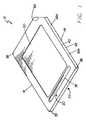
- FIG. 1is an enlarged isometric view of a semiconductor card of the invention
- FIG. 2is an enlarged plan view of a semiconductor card fabricated in accordance with the invention.
- FIG. 3is an enlarged bottom view of a semiconductor card fabricated in accordance with the invention.
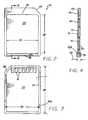
- FIG. 4is an enlarged side cross-sectional view of a semiconductor card fabricated in accordance with the invention, as taken along line 4 - 4 of FIG. 2;
- FIG. 4Ais an enlarged side cross-sectional view of a portion of a semiconductor card in accordance with the invention, as taken from portion 4 A of FIG. 4;
- FIG. 4Bis an enlarged side cross-sectional view of a portion of a semiconductor card in accordance with the invention, as taken from portion 4 B of FIG. 4;
- FIG. 5is an enlarged plan view of a semiconductor card on a strip in accordance with the invention.
- FIG. 6is an enlarged isometric view of a molding apparatus for forming a semiconductor card in accordance with the invention.
- FIG. 7is an enlarged plan view of a lower plate of a molding apparatus for forming a semiconductor card in accordance with the invention.
- FIG. 8is a further enlarged plan view of a lower plate of a molding apparatus of the invention, as taken from portion 8 of FIG. 7;
- FIG. 9is a cross-sectional side view of a portion of a lower plate of a molding apparatus of the invention, as taken along line 9 - 9 of FIG. 8;
- FIG. 10is an enlarged plan view of the lower side of an upper plate of a molding apparatus for forming a semiconductor card in accordance with the invention.
- FIG. 11is a further enlarged plan view of the lower side of an upper plate of a molding apparatus of the invention, as taken from portion 11 of FIG. 10;
- FIG. 12is a cross-sectional side view of a portion of an upper plate of the invention, as taken along line 12 - 12 of FIG. 11;
- FIG. 13is a cross-sectional side view of a portion of an upper plate of the invention, with an inserted down-set pin, as taken along line 12 - 12 of FIG. 11;
- FIG. 14is a further enlarged plan view of the lower side of an upper plate of a molding apparatus of the invention, as taken from portion 14 of FIG. 10;
- FIG. 15is a cross-sectional side view of a portion of an upper plate of the invention, as taken along line 15 - 15 of FIG. 14;
- FIG. 16is a further enlarged plan view of the lower side of an upper plate of a molding apparatus of the invention, as taken from portion 16 of FIG. 10;
- FIG. 17is a cross-sectional side view of a portion of an upper plate of the invention, as taken along line 17 - 17 of FIG. 16;
- FIG. 18is an enlarged partial cross-sectional end view of a molding apparatus of the invention illustrating a configuration of the molding cavity for fabrication of a plastic body on a substrate;
- FIG. 19is an enlarged partial cross-sectional end view of a molding apparatus of the invention illustrating a configuration of the molding cavity for fabrication of a plastic body on a substrate;
- FIG. 20is an enlarged partial cross-sectional end view of a molding apparatus of the invention illustrating a configuration of the molding cavity for fabrication of a plastic body on a substrate;
- FIG. 21is an enlarged plan view of a mold casting of the semiconductor card and attached frame of the invention, prior to singulation;
- FIG. 22is an enlarged lower end view of a molded semiconductor card and attached frame of the invention, prior to singulation;
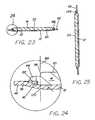
- FIG. 23is an enlarged cross-sectional end view of a molded semiconductor card and attached frame of the invention, prior to singulation, as taken along section line 23 - 23 of FIG. 21;
- FIG. 24is an enlargement of portion 24 of FIG. 23.
- FIG. 25is an enlarged cross-sectional side view of a molded semiconductor card and attached frame of the invention, prior to singulation, as taken along section line 25 - 25 of FIG. 21.
- FIGS. 1 through 4illustrate an improved semiconductor card 10 constructed in accordance with the invention.
- the card 10includes a substrate 12 (see FIG. 4) and at least one semiconductor element 16 (see FIG. 4) mounted to the substrate.
- the semiconductor card 10also includes a plastic body 14 which is molded to portions of the substrate 12 , and an array of external contacts 18 (see FIG. 3) on the substrate 12 for electrical connection with another circuit.
- a semiconductor card 10 containing memorye.g. flash memory
- card 10has a length 24 , width 26 and thickness 28 .
- the thickness 28may typically be set at a desirable value in the range of about 1 mm to about 6 mm.
- the length, width, thickness and other aspects of the cardmay be set by an industry standards group, or alternatively the card configuration is decided by each manufacturer.
- the card 10has a length 24 of about 32 mm., a width 26 of about 24 mm., and a typical thickness 28 of about 1-3 mm.
- the exemplary cardmay include a slightly depressed label area 30 for attachment or inking of a label (not shown) on the front face 20 .
- the label area 30is shown with an exemplary height 32 and width 34 .
- the front face 20 and back face 22 of the semiconductor card 10are joined by a peripheral edge 36 having rounded corners 38 .
- the longitudinal edge 40 about the front face 20 , and the longitudinal edge 42 about the back face 22are shown as rounded to a radius 21 of e.g. about 0.20 mm. for ease of use. See FIG. 4A.
- the edges 40 and 42may be alternatively “drafted” by molding an oblique face 23 on the edge.
- a groove 76is formed in the front face 20 , acting as a finger grip for ease of handling.
- a module 48 including substrate 12is depicted as a thin sheet formed of an electrically insulating material such as an organic polymer resin reinforced with glass fibers.
- Suitable materials for the module 48include bismaleimide-triazine (BT), epoxy resins (e.g. “FR — 4” and “FR-5”), and polyimide resins. Any of these materials can be formed as a sheet of the desired thickness, and then punched, machined or otherwise formed with a required peripheral configuration and with other desired features.
- a representative thickness of the sheet of module 48can be from about 0.2 mm to 1.6 mm.
- the substrate 12 and surrounding frame 46 togethercomprise the module 48 having a width 50 and length 52 .
- the module 48may initially be a segment of a strip 44 which is used to fabricate several cards 10 at the same time.
- One or more substrates 12may be formed from a strip 44 , each substrate being defined by a peripheral opening 54 with inner edge 176 and outer edge 174 .
- Non-substrate portions of the module 48 which surround the substrate 12are herein denoted as a frame 46 .
- the width 84 of the peripheral opening 54is configured so that the peripheral outline 70 (hatched line of FIG. 5) of the produced card 10 lies within the peripheral opening.
- the substrate 12is connected to the frame 46 (and supported thereby) by a plurality of connecting segments 56 , which are similar to tie bars used in lead frames for semiconductor manufacture.
- the peripheral opening 54is shown as extending into the frame 46 on both sides of each connecting segment 56 , in order to provide a desired segment length 58 .
- a width 68 of each connecting segment 56is provided which supports the substrate 12 during processing.
- the module 48 containing substrate 12includes indexing openings 78 for aligning the substrate 12 with a cutting tool, not shown, and a molding apparatus 80 , described infra.
- the module 48may contain other openings 82 for other purposes.
- the peripheral opening 54may be cut in module 48 to provide substrate 12 with a generally rectangular peripheral shape but with one chamfered comer 60 .
- the resulting card 10includes a chamfered comer 66 .
- the purpose of chamfered comer 66is to generally identify the end of the card 10 having external contacts 18 , and ensure that a user inserts the card in a proper orientation.
- the inventionapplies to a card 10 or a substrate 12 of any shape.
- Also shown in FIG. 1are exposed ends 56 A of connecting segments 56 in the as-molded card 10 after molding of the plastic body 14 and singulation from the frame 46 . See also FIG. 3.
- the substrate 12includes a circuit side 62 (FIG. 5) and an opposing back side 64 (see FIG. 3) which in this embodiment comprises the card's backface 22 .
- a longitudinal center line 94 of strip 44and a longitudinal center line 96 of module 48 are shown for reference.
- a peripheral edge 72joins the circuit side 62 and the back side 64 of the substrate 12 .
- the circuit side 62has mounted therein semiconductor components 16 as well as electrical components 74 such as resisters, capacitors, and inductors.
- a circuitis completed by connecting the semiconductor components 16 , electrical components 74 and external contacts 18 (see FIG. 3) with a pattern of conductors, e.g.
- the circuit on the substrate 12may be configured to perform a desired function such as for example, memory storage, sound production, video production, games, product identification, etc.
- the external contacts 18are configured for mating electrical engagement with corresponding contacts (not shown) on a mother board circuit or other electrical assembly (not shown). As illustrated, the external contacts 18 may be planar pads formed of a non-oxidizing conductive material such as gold. However, other configurations for the external contacts 18 may be used, including bumps, pins, or pillars, for example, where the particular application permits.
- components 16 and 74 together with other apparatus on the circuit side 62are encapsulated with a glob-top material which is cured prior to forming the outer card surfaces. No such encapsulation is utilized in the present invention.
- a method of the inventionprovides for a single encapsulation step by precise molding which simultaneously encapsulates active components 16 , 74 on the circuit side 62 of the substrate 12 and forms smooth outer surfaces of the card 10 including rounded or drafted (angular) peripheral card edges 36 .
- semiconductor card 10 of the inventionincludes a plastic body 14 which is molded directly to the circuit side 62 of substrate 12 , covering semiconductor component(s) 16 , electrical component(s) 74 and exposed conductors, bond pads, etc. which are mounted thereon.
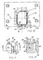
- the molding assembly 80is of a type generally characterized as a transfer mold with mating first (e.g. lower) plate 84 and second (e.g. upper) plate 86 with an interface 88 intermediate the two plates.
- first (e.g. lower) plate 84 and second (e.g. upper) plate 86with an interface 88 intermediate the two plates.
- such molding assembly 80will include an internal mold cavity 100 having internal surfaces 160 A, 160 B in the lower plate 84 and upper plate 86 , respectively (see FIGS.
- the molding assembly 80is modified in accordance with the invention to include a plurality of down-set pins 102 (see FIGS. 10 - 13 , and 18 ) which may be inserted downward along axes 104 in holes 106 passing through the upper plate 86 , as explained further below.
- the molding assembly 80is modified to form wings 148 of molded plastic material; the wings 148 extend laterally from areas between the rounded or drafted card edges 40 , 42 along portions of the card's peripheral edge 36 . Following extraction from the molding apparatus 64 , the wings 92 are excised by a smooth cut about the card's peripheral edge 36 , providing a card 10 with very little if any flash material, and with generally smooth edges 40 and 42 .
- FIGS. 7 through 9show the first (lower) plate 84 of a representative molding assembly 80 for forming a card 10 from a substrate 12 .
- the first plate 84has an upper side 140 with an internal mold surface 160 A, and a lower side or base 138 .
- the first plate 84includes a peripheral raised portion 108 to hold a module frame 46 at a first level 110 .
- the outer edge 122 of peripheral raised portion 108may be dimensionally smaller than the module 48 .
- a depressed portion 112 laterally inside of the raised portion 108is configured to accept a substrate 12 at lower level 114 , with space for forming a plastic periphery about the substrate.
- the substrateis connected to the frame 46 by connecting segments 56 .
- Portions 116 of the depressed portion 112may be depressed further to accommodate external contacts 18 protruding from the backside 64 of the substrate 12 .
- a lower edge portion 118 of the lower mold plate 84Laterally intermediate the raised portion 108 and the depressed portion 112 is a lower edge portion 118 of the lower mold plate 84 .
- the lower edge portion 118has an inner arcuate surface 120 for forming rounded corners 38 and rounded edges 40 , 42 on the card 10 .
- the lower edge portion 118passes upward through the peripheral opening 54 of the module 48 , and in some locations, its upper surface 124 generally abuts the upper plate 86 to form a flash free seam on the peripheral edge 36 of the card 10 .
- a plurality of slits 126are formed through the lower edge portion 118 and raised peripheral portion 126 for passage of connecting segments 56 of the module 48 therethrough.
- the numbers and locations of the slits 126 (and matching substrate segments 56 )provide for downwardly motivated support of the substrate 12 in the depressed portion 112 .
- FIGS. 10 through 17illustrate an upper molding plate 86 configured to contact the circuit side 62 of the substrate 12 .
- the upper molding plate 86has and upper side 142 and a lower side 144 .
- the plate 86is inverted in the figures for viewing the internal mold cavity 100 with an internal mold surface 160 B in the lower side 144 .
- References to portions of the secondi.e.
- upper plate 86as being “raised” or “depressed” refer to the plate as in the inverted position, i.e. with the lower side 142 facing up, and the upper side 140 facing downward. This is particularly evident in the sectional views in FIGS. 12, 13, 15 and 17 .
- the mold cavity 100includes a central depressed region 134 defined by arcuate or drafted walls 136 .
- outward cavity extensions or “wing cavities” 150are shown on four sides of the central depressed region 134 .
- Each wing cavity 150has an outer sloped or rounded wall 152 for ease of mold release.
- the central depressed region 134is at a level 154 below the level 158 of side 144 .
- a step 146 upward from region 134attains an intermediate level 156 forming the base of each wing cavity 150 .
- each injection port 130may communicate with a runner 130 A and a gate 130 B for introducing liquified polymer 15 into the mold cavity 100 at a controlled rate.
- the molding assembly 80may also include vents, not shown, for discharging air from the runners 130 A and mold cavity 100 , as known in the art.
- Another feature of the upper plate 86comprises a plurality of down-set pin through-holes 106 , each located above a connecting segment 56 . See FIGS. 10, 11, 12 and 13 .
- a down-set pin 102may be inserted in each hole 106 to motivate the connecting segments 56 and attached substrate 12 downward into and against the depressed portion 110 . Entry of liquid polymer to the backside 22 of the substrate 12 is thus prevented.
- the down-set holes 106 and pins 102are positioned entirely within the wing cavities 150 , outside of the peripheral edge 36 of the card 10 .
- the pin 102is shown as being generally cylindrical with an outer end 166 and an inner end 164 which may be of reduced size.
- the inner end 164is shown as having a hemispherical shape with chamfered edges, but any shape which effectively clamps a connecting segment 56 against the depressed portion 110 may be utilized.
- the inner end 164may be square, rectangular, quarter round, lunate, etc.
- the holes 106 and down-set pins 102are preferably configured so that the inserted pins 102 are always in the same position relative to the substrate 12 . As shown herein, the configuration of the molding apparatus 80 and the configuration of module 48 must be compatible.
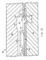
- FIGS. 18, 19 and 20show portions of a molding apparatus 80 assembled for forming an encapsulating polymeric body 14 on a substrate 12 of a module 48 .
- the dimensions of various partsare not necessarily to scale.
- a module 48is shown inserted between the upper side 140 of a first or lower plate 84 and the lower side 144 of a second or upper plate 86 .
- the module sectionis shown with a frame 46 , a substrate 12 , and one of the four connecting segments 56 linking the substrate to the frame.
- the connecting segment 56has an inner end 170 and an outer end 172 .
- the connecting segment 56is shown pushed downward by the inner end 164 of one of the down-set pins 102 into the depressed portion 112 of the lower plate 84 .
- the displacement 155 of the substrate 12 from the frame 46may be small, i.e. about 1 ⁇ 5 of the substrate thickness 13 , or may be up to about 3 times the substrate thickness, depending on the thicknesses of substrate and card 10 .
- the substrate 12is shown with a circuit side 62 on which are mounted exemplary semiconductor components 16 with connecting bond wires 17 .
- the substrate 12is held downward to portion 112 by the connecting segments 56 , generally preventing passage of polymeric mold compound 15 onto the substrate's backside 64 .
- the peripheral opening 54 over the majority of the substrate 12generally has a width 55 extending from the inner end 170 to the opening's outer edge 174 (see also FIGS. 19 and 20).
- FIG. 18the region 134 forming the front face of the molded card 10 is shown with a slightly indented area 30 in which a label may be applied.
- FIG. 18depicts a final singulation plane 168 relative to the molding assembly 80 .
- the semiconductor card 10will be singulated from the frame 46 and wings 148 following removal from the molding assembly 80 .
- the unsingulated card 10may be ejected from the mold by further insertion of down-set pins 102 , or use of other pins, not shown. Ease of ejection is enabled by the use of sloped lateral surfaces and rounded or oblique corners on the molded casting 180 .
- FIG. 19depicts the molding assembly 80 with the module frame 46 and substrate 12 at a position away from a connecting segment 56 . Shown are wing cavities 150 in which wings 148 are formed.
- the lower edge portion 118which surrounds the mold cavity 100 in the lower plate 84 fits within the peripheral opening 54 between edges 174 and 176 .
- the lower edge portion 118molds an arcuate or oblique comer surface 120 on the molded card 10 .
- FIG. 20depicts the molding assembly 80 , substrate 12 and module frame 46 in a portion where there is a substantial absence of wing cavities 150 , and the substrate has external contacts 18 on its back side 64 .
- a cavity 178is formed in the lower plate 84 into which the contacts 18 fit.
- the external contacts, or even the entire back side 64may in addition be covered by tape or other protective membe (not shown) to ensure freedom from flash material on the card's back side.
- FIG. 21a casting 180 molded on a semiconductor card module 48 is shown in front view following removal from the molding assembly 80 .
- the card module 48includes a molded card body 14 with molded wings 148 extending outwardly therefrom along major peripheral edges 36 .
- the card body 14has a width 26 and length 24 .
- the peripheral openings 54are now filled with hardened molding material 15 , including on both sides of each connecting segment 56 .
- the card body 14is connected to the module 48 along a central portion of its peripheral edges 36 , and its upper and lower peripheral edges 40 , 42 are smooth, rounded or oblique, and substantially free of “flash” material. This is evident by examination of FIGS. 22, 23, 24 and 25 .
- the card 10has a back side 22 comprising the back side 64 of the substrate 12 .
- the semiconductor card 10is singulated from the module 48 by cutting it free along its peripheral edges 36 , i.e. through the wings 148 , by saw, erosion process or other cutting tool.
- the four small ends 56 A of the connecting segments 56which project from card edges 56 may be easily trimmed (if desired) by clipping or other methods. Alternatively, the ends 56 A may be pre-scored, i.e. prior to molding, to minimize protrusion of the ends 56 A from the card edges 56 .
- a strip 44 of a dielectric materialis provided in sheet form
- a peripheral opening 54is formed in at least one portion of the strip 44 designated as a module 48 , in which the opening 54 defines the boundaries of a substrate 12 . Opposing sides of the substrate 12 is connected to a frame portion 46 of the module 48 by connecting segments 56 of the module 48 . Other openings 82 for indexing and handling are also provided.
- a circuit 73is formed on the “circuit” side 62 of the substrate 12 , including at least one semiconductor component 16 as well as electrical component(s) 74 and interconnecting conductors.
- External contacts 18are formed on the back side 64 of the substrate 12 and connected to circuit 73 .
- a set of mold plates 84 , 86is configured for molding a polymeric body peripherally 14 about the circuitized substrate 12 and over portions of the circuit side 62 thereof.
- Down-set pin holes 106are provided outside of the card outline 70 in an upper mold plate 86 for insertion of pins 102 to motivate the connecting segments 56 (and attached substrate 12 ) downward to a lower level against a lower surface of the internal molding cavity 100 in the lower mold plate 84 .
- the lower mold plate 84 and upper mold plate 86are assembled with module 48 therebetween.
- the molding assembly 80is connected to a supply of molding compound and clamped shut.
- Down-set pins 102are positioned in the holes 106 to force the substrate 12 downward to a seated position.
- Fluid polymeric molding compound 15is introduced into the molding assembly 80 under conditions which rapidly fill the mold cavity 100 , encapsulating the circuit 73 and forming a plastic body 14 .
- the card 10is singulated from its module 48 by cutting along the card outline 70 .
- exposed ends 56 A of the connecting segments 56 within the card 10may be cut back. If necessary, flash residue may be removed.
- the molding assembly 80may be configured to cover portions of both sides 20 , 22 of a substrate 12 .
- the molding cavity 100 of lower plate 84is varied by providing one or more additional cavities and associated runners for introducing bonding compound 15 .
- the inventionprovides a semiconductor card by a method which eliminates a separate glob top encapsulation step, and ensures smooth card edges which are rounded or oblique. Desired card dimensions are readily maintained, and flash material requiring removal is minimized. If desired, the molding assembly may be configured to form several cards simultaneously.
Landscapes
- Engineering & Computer Science (AREA)
- Microelectronics & Electronic Packaging (AREA)
- Manufacturing & Machinery (AREA)
- General Physics & Mathematics (AREA)
- Physics & Mathematics (AREA)
- Condensed Matter Physics & Semiconductors (AREA)
- Mechanical Engineering (AREA)
- Computer Hardware Design (AREA)
- Power Engineering (AREA)
- Encapsulation Of And Coatings For Semiconductor Or Solid State Devices (AREA)
- Injection Moulding Of Plastics Or The Like (AREA)
- Credit Cards Or The Like (AREA)
- Moulds For Moulding Plastics Or The Like (AREA)
Abstract
Description
- 1. Field of the Invention[0001]
- This invention relates generally to semiconductor manufacture. More particularly, the invention pertains to an improved semiconductor card, and to improved methods and systems for fabricating the card.[0002]
- 2.State of the Art[0003]
- One type of electronic assembly containing semiconductor components is generally referred to as a “card”. Examples of such “cards” include multi media cards such as used in digital cameras and the like, memory cards, smart cards, and personal computer memory card international association (PCMCIA) cards. The instant patent application refers to these types of cards as “semiconductor cards”. These cards are sometimes referred to as “daughter boards”.[0004]
- Typically, a semiconductor card comprises a substrate which may be a thin printed circuit board (PCB) upon which electronic components are mounted. Such components may include, for example, at least one semiconductor die and/or die package as well as resistors, capacitors, inductors and the like to form a desired circuitry. The substrate includes conductors for providing power supply and interconnection of the various components. Typically, the components are mounted on one side, i.e. “circuit” side of the substrate, and are electrically interconnected to external contacts on the opposing side by interlevel conductors. The external contacts are arranged for electrical contact with a next level package, i.e. mother board. In use in an exemplary electronic apparatus such as a digital camera, the card may be inserted into a slot or other receiver for interconnection with a motherboard, and provide for example, flash memory for digitally recording images.[0005]
- Semiconductor cards are typically intended for repeated handling by the public, necessitating protection of the components from mechanical forces, moisture, radiation and stray electrical currents. In the industry, the semiconductor components and interconnecting conductors on the circuit side of a card substrate have typically been encapsulated by first applying “glob top” encapsulant. Then, a separately formed protective cover produced by injection molding is adhesively attached over the circuit side of the substrate to form the semiconductor card. However, use of a separately formed cover not only adds undesirable thickness to the card, it requires additional process steps, and is subject to deleterious detachment of the cover from the substrate. In addition, any variation in mounted component height and overlying glob top material will result in card thickness variation.[0006]
- For most applications, it is desirable to make the card as thin as possible. The use of thin cards saves space within the equipment in which the card is used, as well as storage space, and a saving in encapsulation material is also realized.[0007]
- A further requirement for semiconductor cards is that the peripheral outlines and card dimensions be as uniform as possible, so that proper effective insertion into a card receiver is assured. Specifications on the peripheral outline and dimensions of semiconductor cards have been set by various industry standard setting bodies, e.g. PCMCIA.[0008]
- In present methods of manufacture, components for several semiconductor cards are fabricated and wire bonded on a strip of e.g. circuit board. The strip may be viewed as equivalent to the lead frame in die manufacture. The individual cards are then separated from the strip using a singulation process such as sawing. Often the singulation step produces slivers, and forms substrate edges which are rough or sharp. These defects can adversely affect the peripheral outline, dimensions, appearance and use of the card.[0009]
- The need exists for a method to encapsulate a semiconductor card whereby the card has reduced thickness as well as less variation thereof. In addition, the desired method will produce a card with improved precision in peripheral outline, dimensions and appearance, and at lower cost.[0010]
- In accordance with the present invention, an improved semiconductor card is provided. In addition, a method and a system for fabricating the improved card are disclosed.[0011]
- The semiconductor card includes a substrate such as a printed circuit board (PCB). The substrate comprises an electrically insulative material such as an organic polymer resin reinforced with glass fibers, and may include more than one layer. The substrate has a circuit side with a pattern of conductors thereon, and an opposing back side with a pattern of external contacts thereon. Electronic components such as semiconductor dice, resistors, capacitors, and the like are formed or mounted on the circuit side of the substrate. The semiconductor dice may comprise bare dice wire bonded to the conductors, bumped dice flip chip mounted to the conductors, or semiconductor packages bonded to the conductors. A single molding step serves to encapsulate the circuit side of the substrate and simultaneously form card surfaces and edges with smooth rounded or oblique corners.[0012]
- A substrate may be initially formed as a segment of a substrate strip containing more than one module having a substrate separated therefrom by a peripheral opening. The strip is similar in function to a semiconductor lead frame, and permits various fabrication processes to be performed on one or more substrate at the same time. The substrate is connected to the strip with connecting segments similar to tie bars on a semiconductor lead frame.[0013]
- A molding assembly is adapted to form a plastic body larger than the substrate, and simultaneously encapsulates circuit components such as dice, resistors, capacitors, bond wires, etc. on the substrate as the card body is formed. Plastic wings are also formed by molding, extending outwardly from a central portion of the card edges along major sides of the card periphery.[0014]
- Prior to introducing molding compound, a plurality of down-set pins are inserted downward through the upper plate, outside of the card periphery, to depress the connecting segments and attached substrate downward into a cavity. The resulting substrate will be lower than the frame portion of the module, and provide the back side of the semiconductor card.[0015]
- Following molding, the casting is removed and desingulated by cutting off the wings.[0016]
- The method is much simpler and quicker than the prior method in which the circuit side of a card is glob topped and then covered by a separately molded cap which is cemented thereto.[0017]
- FIG. 1 is an enlarged isometric view of a semiconductor card of the invention;[0018]
- FIG. 2 is an enlarged plan view of a semiconductor card fabricated in accordance with the invention;[0019]
- FIG. 3 is an enlarged bottom view of a semiconductor card fabricated in accordance with the invention;[0020]
- FIG. 4 is an enlarged side cross-sectional view of a semiconductor card fabricated in accordance with the invention, as taken along line[0021]4-4 of FIG. 2;
- FIG. 4A is an enlarged side cross-sectional view of a portion of a semiconductor card in accordance with the invention, as taken from[0022]
portion 4A of FIG. 4; - FIG. 4B is an enlarged side cross-sectional view of a portion of a semiconductor card in accordance with the invention, as taken from portion[0023]4B of FIG. 4;
- FIG. 5 is an enlarged plan view of a semiconductor card on a strip in accordance with the invention;[0024]
- FIG. 6 is an enlarged isometric view of a molding apparatus for forming a semiconductor card in accordance with the invention;[0025]
- FIG. 7 is an enlarged plan view of a lower plate of a molding apparatus for forming a semiconductor card in accordance with the invention;[0026]
- FIG. 8 is a further enlarged plan view of a lower plate of a molding apparatus of the invention, as taken from portion[0027]8 of FIG. 7;
- FIG. 9 is a cross-sectional side view of a portion of a lower plate of a molding apparatus of the invention, as taken along line[0028]9-9 of FIG. 8;
- FIG. 10 is an enlarged plan view of the lower side of an upper plate of a molding apparatus for forming a semiconductor card in accordance with the invention;[0029]
- FIG. 11 is a further enlarged plan view of the lower side of an upper plate of a molding apparatus of the invention, as taken from portion[0030]11 of FIG. 10;
- FIG. 12 is a cross-sectional side view of a portion of an upper plate of the invention, as taken along line[0031]12-12 of FIG. 11;
- FIG. 13 is a cross-sectional side view of a portion of an upper plate of the invention, with an inserted down-set pin, as taken along line[0032]12-12 of FIG. 11;
- FIG. 14 is a further enlarged plan view of the lower side of an upper plate of a molding apparatus of the invention, as taken from[0033]
portion 14 of FIG. 10; - FIG. 15 is a cross-sectional side view of a portion of an upper plate of the invention, as taken along line[0034]15-15 of FIG. 14;
- FIG. 16 is a further enlarged plan view of the lower side of an upper plate of a molding apparatus of the invention, as taken from[0035]
portion 16 of FIG. 10; - FIG. 17 is a cross-sectional side view of a portion of an upper plate of the invention, as taken along line[0036]17-17 of FIG. 16;
- FIG. 18 is an enlarged partial cross-sectional end view of a molding apparatus of the invention illustrating a configuration of the molding cavity for fabrication of a plastic body on a substrate;[0037]
- FIG. 19 is an enlarged partial cross-sectional end view of a molding apparatus of the invention illustrating a configuration of the molding cavity for fabrication of a plastic body on a substrate;[0038]
- FIG. 20 is an enlarged partial cross-sectional end view of a molding apparatus of the invention illustrating a configuration of the molding cavity for fabrication of a plastic body on a substrate;[0039]
- FIG. 21 is an enlarged plan view of a mold casting of the semiconductor card and attached frame of the invention, prior to singulation;[0040]
- FIG. 22 is an enlarged lower end view of a molded semiconductor card and attached frame of the invention, prior to singulation;[0041]
- FIG. 23 is an enlarged cross-sectional end view of a molded semiconductor card and attached frame of the invention, prior to singulation, as taken along section line[0042]23-23 of FIG. 21;
- FIG. 24 is an enlargement of[0043]
portion 24 of FIG. 23; and - FIG. 25 is an enlarged cross-sectional side view of a molded semiconductor card and attached frame of the invention, prior to singulation, as taken along section line[0044]25-25 of FIG. 21.
- The invention is described and illustrated herein below in terms of a[0045]
semiconductor card 10 which is exemplified by a “multimedia card”. FIGS. 1 through 4 illustrate animproved semiconductor card 10 constructed in accordance with the invention. Thecard 10 includes a substrate12 (see FIG. 4) and at least one semiconductor element16 (see FIG. 4) mounted to the substrate. Thesemiconductor card 10 also includes aplastic body 14 which is molded to portions of thesubstrate 12, and an array of external contacts18 (see FIG. 3) on thesubstrate 12 for electrical connection with another circuit. Thus, for example, asemiconductor card 10 containing memory (e.g. flash memory) may be configured for removable insertion into photographic devices for digital recording and retrievable storage of still pictures or video, and optionally audio. - As shown in FIGS.[0046]1-4,
card 10 has alength 24,width 26 andthickness 28. Thethickness 28 may typically be set at a desirable value in the range of about 1 mm to about 6 mm. In an exemplarymulti media card 10 described herein, the length, width, thickness and other aspects of the card may be set by an industry standards group, or alternatively the card configuration is decided by each manufacturer. In the particular example shown, thecard 10 has alength 24 of about 32 mm., awidth 26 of about 24 mm., and atypical thickness 28 of about 1-3 mm. As depicted in FIGS. 1 and 2, the exemplary card may include a slightlydepressed label area 30 for attachment or inking of a label (not shown) on thefront face 20. Thelabel area 30 is shown with anexemplary height 32 andwidth 34. - The[0047]
front face 20 and back face22 of thesemiconductor card 10 are joined by aperipheral edge 36 having roundedcorners 38. In accordance with the invention, thelongitudinal edge 40 about thefront face 20, and thelongitudinal edge 42 about theback face 22 are shown as rounded to aradius 21 of e.g. about 0.20 mm. for ease of use. See FIG. 4A. As depicted in FIG. 4B, theedges oblique face 23 on the edge. - As depicted in FIGS. 1, 2, and[0048]4, a
groove 76 is formed in thefront face 20, acting as a finger grip for ease of handling. - In FIG. 5, a[0049]
module 48 includingsubstrate 12 is depicted as a thin sheet formed of an electrically insulating material such as an organic polymer resin reinforced with glass fibers. Suitable materials for themodule 48 include bismaleimide-triazine (BT), epoxy resins (e.g. “FR —4” and “FR-5”), and polyimide resins. Any of these materials can be formed as a sheet of the desired thickness, and then punched, machined or otherwise formed with a required peripheral configuration and with other desired features. A representative thickness of the sheet ofmodule 48 can be from about 0.2 mm to 1.6 mm. Thesubstrate 12 and surroundingframe 46 together comprise themodule 48 having awidth 50 andlength 52. Themodule 48 may initially be a segment of astrip 44 which is used to fabricateseveral cards 10 at the same time. One ormore substrates 12 may be formed from astrip 44, each substrate being defined by aperipheral opening 54 withinner edge 176 andouter edge 174. Non-substrate portions of themodule 48 which surround thesubstrate 12 are herein denoted as aframe 46. Thewidth 84 of theperipheral opening 54 is configured so that the peripheral outline70 (hatched line of FIG. 5) of the producedcard 10 lies within the peripheral opening. Thesubstrate 12 is connected to the frame46 (and supported thereby) by a plurality of connectingsegments 56, which are similar to tie bars used in lead frames for semiconductor manufacture. Theperipheral opening 54 is shown as extending into theframe 46 on both sides of each connectingsegment 56, in order to provide a desiredsegment length 58. Awidth 68 of each connectingsegment 56 is provided which supports thesubstrate 12 during processing. Themodule 48 containingsubstrate 12 includesindexing openings 78 for aligning thesubstrate 12 with a cutting tool, not shown, and amolding apparatus 80, described infra. Themodule 48 may containother openings 82 for other purposes. - As shown in FIG. 5, the[0050]
peripheral opening 54 may be cut inmodule 48 to providesubstrate 12 with a generally rectangular peripheral shape but with one chamferedcomer 60. As shown in FIG. 1, the resultingcard 10 includes a chamferedcomer 66. The purpose ofchamfered comer 66 is to generally identify the end of thecard 10 havingexternal contacts 18, and ensure that a user inserts the card in a proper orientation. However, the invention applies to acard 10 or asubstrate 12 of any shape. Also shown in FIG. 1 are exposedends 56A of connectingsegments 56 in the as-moldedcard 10 after molding of theplastic body 14 and singulation from theframe 46. See also FIG. 3. - The[0051]
substrate 12 includes a circuit side62 (FIG. 5) and an opposing back side64 (see FIG. 3) which in this embodiment comprises the card'sbackface 22. In FIG. 5, alongitudinal center line 94 ofstrip 44, and alongitudinal center line 96 ofmodule 48 are shown for reference. A peripheral edge72 joins thecircuit side 62 and theback side 64 of thesubstrate 12. As illustrated in theexemplary substrate 12 of FIG. 5, thecircuit side 62 has mounted thereinsemiconductor components 16 as well aselectrical components 74 such as resisters, capacitors, and inductors. A circuit is completed by connecting thesemiconductor components 16,electrical components 74 and external contacts18 (see FIG. 3) with a pattern of conductors, e.g. wires, printed conductors, vias, and the like, not shown in the figures. Contacts (not shown) may also be provided to establish test circuits for example, typically on thecircuit side 62 of the substrate. Methods and apparatus for forming, attaching and conductively interconnectingcomponents substrate 12 may be configured to perform a desired function such as for example, memory storage, sound production, video production, games, product identification, etc. - The[0052]
external contacts 18 are configured for mating electrical engagement with corresponding contacts (not shown) on a mother board circuit or other electrical assembly (not shown). As illustrated, theexternal contacts 18 may be planar pads formed of a non-oxidizing conductive material such as gold. However, other configurations for theexternal contacts 18 may be used, including bumps, pins, or pillars, for example, where the particular application permits. - In other processes for making[0053]
semiconductor cards 10,components circuit side 62 are encapsulated with a glob-top material which is cured prior to forming the outer card surfaces. No such encapsulation is utilized in the present invention. As described herein, a method of the invention provides for a single encapsulation step by precise molding which simultaneously encapsulatesactive components circuit side 62 of thesubstrate 12 and forms smooth outer surfaces of thecard 10 including rounded or drafted (angular) peripheral card edges36. - Regardless of the particular application to which the card circuit is directed,[0054]
semiconductor card 10 of the invention includes aplastic body 14 which is molded directly to thecircuit side 62 ofsubstrate 12, covering semiconductor component(s)16, electrical component(s)74 and exposed conductors, bond pads, etc. which are mounted thereon. As shown in FIG. 6, themolding assembly 80 is of a type generally characterized as a transfer mold with mating first (e.g. lower)plate 84 and second (e.g. upper)plate 86 with aninterface 88 intermediate the two plates. As known in the art,such molding assembly 80 will include aninternal mold cavity 100 havinginternal surfaces 160A,160B in thelower plate 84 andupper plate 86, respectively (see FIGS. 7 and 10), andalignment apertures 90 for precise joining of the plates. In addition, there areopenings 92 for introduction of flowable polymeric molding compound (not shown) into themold cavity 100. In addition, themolding assembly 80 is modified in accordance with the invention to include a plurality of down-set pins102 (see FIGS.10-13, and18) which may be inserted downward alongaxes 104 inholes 106 passing through theupper plate 86, as explained further below. - Furthermore, the[0055]
molding assembly 80 is modified to formwings 148 of molded plastic material; thewings 148 extend laterally from areas between the rounded or drafted card edges40,42 along portions of the card'speripheral edge 36. Following extraction from themolding apparatus 64, thewings 92 are excised by a smooth cut about the card'speripheral edge 36, providing acard 10 with very little if any flash material, and with generallysmooth edges - Turning now to FIGS. 7 through 9, which show the first (lower)[0056]
plate 84 of arepresentative molding assembly 80 for forming acard 10 from asubstrate 12. Thefirst plate 84 has anupper side 140 with an internal mold surface160A, and a lower side orbase 138. Thefirst plate 84 includes a peripheral raisedportion 108 to hold amodule frame 46 at afirst level 110. Theouter edge 122 of peripheral raisedportion 108 may be dimensionally smaller than themodule 48. Adepressed portion 112 laterally inside of the raisedportion 108 is configured to accept asubstrate 12 atlower level 114, with space for forming a plastic periphery about the substrate. The substrate is connected to theframe 46 by connectingsegments 56.Portions 116 of thedepressed portion 112 may be depressed further to accommodateexternal contacts 18 protruding from thebackside 64 of thesubstrate 12. Laterally intermediate the raisedportion 108 and thedepressed portion 112 is alower edge portion 118 of thelower mold plate 84. Thelower edge portion 118 has an innerarcuate surface 120 for formingrounded corners 38 and roundededges card 10. Thelower edge portion 118 passes upward through theperipheral opening 54 of themodule 48, and in some locations, itsupper surface 124 generally abuts theupper plate 86 to form a flash free seam on theperipheral edge 36 of thecard 10. As shown, a plurality ofslits 126 are formed through thelower edge portion 118 and raisedperipheral portion 126 for passage of connectingsegments 56 of themodule 48 therethrough. The numbers and locations of the slits126 (and matching substrate segments56) provide for downwardly motivated support of thesubstrate 12 in thedepressed portion 112. - FIGS. 10 through 17 illustrate an[0057]
upper molding plate 86 configured to contact thecircuit side 62 of thesubstrate 12. Theupper molding plate 86 has andupper side 142 and alower side 144. Theplate 86 is inverted in the figures for viewing theinternal mold cavity 100 with aninternal mold surface 160B in thelower side 144. Shown arealignment apertures 90, a raised peripheral portion128 (with boundary132) for contacting the upper surface47 offrame 46, andinjection ports 130 alongplate edge 162, through whichpressurized fluid polymer 15 is introduced into the mold cavity (see FIGS. 16 and 17). References to portions of the second i.e.upper plate 86 as being “raised” or “depressed” refer to the plate as in the inverted position, i.e. with thelower side 142 facing up, and theupper side 140 facing downward. This is particularly evident in the sectional views in FIGS. 12, 13,15 and17. - The[0058]
mold cavity 100 includes a centraldepressed region 134 defined by arcuate or draftedwalls 136. In addition, outward cavity extensions or “wing cavities”150 are shown on four sides of the centraldepressed region 134. Eachwing cavity 150 has an outer sloped or roundedwall 152 for ease of mold release. Thus, the centraldepressed region 134 is at alevel 154 below thelevel 158 ofside 144. Astep 146 upward fromregion 134 attains anintermediate level 156 forming the base of eachwing cavity 150. - As shown in FIG. 17, each[0059]
injection port 130 may communicate with arunner 130A and agate 130B for introducingliquified polymer 15 into themold cavity 100 at a controlled rate. Themolding assembly 80 may also include vents, not shown, for discharging air from therunners 130A andmold cavity 100, as known in the art. - Another feature of the[0060]
upper plate 86 comprises a plurality of down-set pin through-holes 106, each located above a connectingsegment 56. See FIGS. 10, 11,12 and13. A down-set pin 102 may be inserted in eachhole 106 to motivate the connectingsegments 56 and attachedsubstrate 12 downward into and against thedepressed portion 110. Entry of liquid polymer to thebackside 22 of thesubstrate 12 is thus prevented. - The down-set[0061]
holes 106 and pins102 are positioned entirely within thewing cavities 150, outside of theperipheral edge 36 of thecard 10. Thepin 102 is shown as being generally cylindrical with anouter end 166 and aninner end 164 which may be of reduced size. In the figures, theinner end 164 is shown as having a hemispherical shape with chamfered edges, but any shape which effectively clamps a connectingsegment 56 against thedepressed portion 110 may be utilized. For example, theinner end 164 may be square, rectangular, quarter round, lunate, etc. Theholes 106 and down-setpins 102 are preferably configured so that the inserted pins102 are always in the same position relative to thesubstrate 12. As shown herein, the configuration of themolding apparatus 80 and the configuration ofmodule 48 must be compatible. - FIGS. 18, 19 and[0062]20 show portions of a
molding apparatus 80 assembled for forming an encapsulatingpolymeric body 14 on asubstrate 12 of amodule 48. The dimensions of various parts are not necessarily to scale. - In FIG. 18, a[0063]
module 48 is shown inserted between theupper side 140 of a first orlower plate 84 and thelower side 144 of a second orupper plate 86. The module section is shown with aframe 46, asubstrate 12, and one of the four connectingsegments 56 linking the substrate to the frame. The connectingsegment 56 has aninner end 170 and an outer end172. The connectingsegment 56 is shown pushed downward by theinner end 164 of one of the down-setpins 102 into thedepressed portion 112 of thelower plate 84. Thedisplacement 155 of thesubstrate 12 from theframe 46 may be small, i.e. about ⅕ of thesubstrate thickness 13, or may be up to about 3 times the substrate thickness, depending on the thicknesses of substrate andcard 10. - The[0064]
substrate 12 is shown with acircuit side 62 on which are mountedexemplary semiconductor components 16 with connectingbond wires 17. Thesubstrate 12 is held downward toportion 112 by the connectingsegments 56, generally preventing passage ofpolymeric mold compound 15 onto the substrate'sbackside 64. For reference purposes, theperipheral opening 54 over the majority of thesubstrate 12 generally has awidth 55 extending from theinner end 170 to the opening's outer edge174 (see also FIGS. 19 and 20). - In FIG. 18, the[0065]
region 134 forming the front face of the moldedcard 10 is shown with a slightlyindented area 30 in which a label may be applied. In addition, FIG. 18 depicts afinal singulation plane 168 relative to themolding assembly 80. Thesemiconductor card 10 will be singulated from theframe 46 andwings 148 following removal from themolding assembly 80. - Following molding and solidification of the casting in the[0066]
molding assembly 80, theunsingulated card 10 may be ejected from the mold by further insertion of down-setpins 102, or use of other pins, not shown. Ease of ejection is enabled by the use of sloped lateral surfaces and rounded or oblique corners on the moldedcasting 180. - FIG. 19 depicts the[0067]
molding assembly 80 with themodule frame 46 andsubstrate 12 at a position away from a connectingsegment 56. Shown arewing cavities 150 in whichwings 148 are formed. Thelower edge portion 118 which surrounds themold cavity 100 in thelower plate 84 fits within theperipheral opening 54 betweenedges lower edge portion 118 molds an arcuate oroblique comer surface 120 on the moldedcard 10. - FIG. 20 depicts the[0068]
molding assembly 80,substrate 12 andmodule frame 46 in a portion where there is a substantial absence ofwing cavities 150, and the substrate hasexternal contacts 18 on itsback side 64. As shown, acavity 178 is formed in thelower plate 84 into which thecontacts 18 fit. The external contacts, or even the entireback side 64 may in addition be covered by tape or other protective membe (not shown) to ensure freedom from flash material on the card's back side. - In FIG. 21, a casting[0069]180 molded on a
semiconductor card module 48 is shown in front view following removal from themolding assembly 80. Thecard module 48 includes a moldedcard body 14 with moldedwings 148 extending outwardly therefrom along majorperipheral edges 36. Thecard body 14 has awidth 26 andlength 24. Theperipheral openings 54 are now filled with hardenedmolding material 15, including on both sides of each connectingsegment 56. Thecard body 14 is connected to themodule 48 along a central portion of itsperipheral edges 36, and its upper and lowerperipheral edges card 10 has aback side 22 comprising theback side 64 of thesubstrate 12. Thesemiconductor card 10 is singulated from themodule 48 by cutting it free along itsperipheral edges 36, i.e. through thewings 148, by saw, erosion process or other cutting tool. The foursmall ends 56A of the connecting segments56 (see FIG. 1) which project from card edges56 may be easily trimmed (if desired) by clipping or other methods. Alternatively, theends 56A may be pre-scored, i.e. prior to molding, to minimize protrusion of theends 56A from the card edges56. - In the manufacture of the[0070]
semiconductor card 10 of the invention, the steps involved may be summarized as including: - a. A[0071]
strip 44 of a dielectric material is provided in sheet form; - b. A[0072]
peripheral opening 54 is formed in at least one portion of thestrip 44 designated as amodule 48, in which theopening 54 defines the boundaries of asubstrate 12. Opposing sides of thesubstrate 12 is connected to aframe portion 46 of themodule 48 by connectingsegments 56 of themodule 48.Other openings 82 for indexing and handling are also provided. - c. A circuit[0073]73 is formed on the “circuit”
side 62 of thesubstrate 12, including at least onesemiconductor component 16 as well as electrical component(s)74 and interconnecting conductors. - d.[0074]
External contacts 18 are formed on theback side 64 of thesubstrate 12 and connected to circuit73. - e. A set of[0075]
mold plates circuitized substrate 12 and over portions of thecircuit side 62 thereof. Down-set pin holes106 are provided outside of thecard outline 70 in anupper mold plate 86 for insertion ofpins 102 to motivate the connecting segments56 (and attached substrate12) downward to a lower level against a lower surface of theinternal molding cavity 100 in thelower mold plate 84. - f. The[0076]
lower mold plate 84 andupper mold plate 86 are assembled withmodule 48 therebetween. Themolding assembly 80 is connected to a supply of molding compound and clamped shut. - Down-set[0077]
pins 102 are positioned in theholes 106 to force thesubstrate 12 downward to a seated position. - g. Fluid[0078]
polymeric molding compound 15 is introduced into themolding assembly 80 under conditions which rapidly fill themold cavity 100, encapsulating the circuit73 and forming aplastic body 14. - h. After curing and cooling of the[0079]
mold material 15, the mold is opened and the moldedmodule 48 removed therefrom. Pins may be inserted inthroughholes 106 and used as ejection tools for releasing the module. - i. The[0080]
card 10 is singulated from itsmodule 48 by cutting along thecard outline 70. - j. If desired, exposed ends[0081]56A of the connecting
segments 56 within thecard 10 may be cut back. If necessary, flash residue may be removed. - In another embodiment of the invention, the[0082]
molding assembly 80 may be configured to cover portions of bothsides substrate 12. Themolding cavity 100 oflower plate 84 is varied by providing one or more additional cavities and associated runners for introducingbonding compound 15. - As described herein, the invention provides a semiconductor card by a method which eliminates a separate glob top encapsulation step, and ensures smooth card edges which are rounded or oblique. Desired card dimensions are readily maintained, and flash material requiring removal is minimized. If desired, the molding assembly may be configured to form several cards simultaneously.[0083]
- It is apparent to those skilled in the art that various changes and modifications may be made in the manufacturing methods and apparatus of the invention as disclosed herein without departing from the spirit and scope of the invention as defined in the following claims.[0084]
Claims (34)
Priority Applications (4)
| Application Number | Priority Date | Filing Date | Title |
|---|---|---|---|
| US09/878,302US7220615B2 (en) | 2001-06-11 | 2001-06-11 | Alternative method used to package multimedia card by transfer molding |
| US10/928,596US20050023583A1 (en) | 2001-06-11 | 2004-08-26 | Multi media card formed by transfer molding |
| US10/927,678US20050022378A1 (en) | 2001-06-11 | 2004-08-26 | Apparatus used to package multimedia card by transfer molding |
| US11/386,154US20060157838A1 (en) | 2001-06-11 | 2006-03-21 | Multimedia card and transfer molding method |
Applications Claiming Priority (1)
| Application Number | Priority Date | Filing Date | Title |
|---|---|---|---|
| US09/878,302US7220615B2 (en) | 2001-06-11 | 2001-06-11 | Alternative method used to package multimedia card by transfer molding |
Related Child Applications (3)
| Application Number | Title | Priority Date | Filing Date |
|---|---|---|---|
| US10/927,678DivisionUS20050022378A1 (en) | 2001-06-11 | 2004-08-26 | Apparatus used to package multimedia card by transfer molding |
| US10/928,596DivisionUS20050023583A1 (en) | 2001-06-11 | 2004-08-26 | Multi media card formed by transfer molding |
| US11/386,154ContinuationUS20060157838A1 (en) | 2001-06-11 | 2006-03-21 | Multimedia card and transfer molding method |
Publications (2)
| Publication Number | Publication Date |
|---|---|
| US20020186549A1true US20020186549A1 (en) | 2002-12-12 |
| US7220615B2 US7220615B2 (en) | 2007-05-22 |
Family
ID=25371755
Family Applications (4)
| Application Number | Title | Priority Date | Filing Date |
|---|---|---|---|
| US09/878,302Expired - Fee RelatedUS7220615B2 (en) | 2001-06-11 | 2001-06-11 | Alternative method used to package multimedia card by transfer molding |
| US10/928,596AbandonedUS20050023583A1 (en) | 2001-06-11 | 2004-08-26 | Multi media card formed by transfer molding |
| US10/927,678AbandonedUS20050022378A1 (en) | 2001-06-11 | 2004-08-26 | Apparatus used to package multimedia card by transfer molding |
| US11/386,154AbandonedUS20060157838A1 (en) | 2001-06-11 | 2006-03-21 | Multimedia card and transfer molding method |
Family Applications After (3)
| Application Number | Title | Priority Date | Filing Date |
|---|---|---|---|
| US10/928,596AbandonedUS20050023583A1 (en) | 2001-06-11 | 2004-08-26 | Multi media card formed by transfer molding |
| US10/927,678AbandonedUS20050022378A1 (en) | 2001-06-11 | 2004-08-26 | Apparatus used to package multimedia card by transfer molding |
| US11/386,154AbandonedUS20060157838A1 (en) | 2001-06-11 | 2006-03-21 | Multimedia card and transfer molding method |
Country Status (1)
| Country | Link |
|---|---|
| US (4) | US7220615B2 (en) |
Cited By (22)
| Publication number | Priority date | Publication date | Assignee | Title |
|---|---|---|---|---|
| US20050035435A1 (en)* | 2001-08-30 | 2005-02-17 | James Steven L. | Method for fabricating semiconductor components using mold cavities having runners configured to minimize venting |
| US6963142B2 (en) | 2001-10-26 | 2005-11-08 | Micron Technology, Inc. | Flip chip integrated package mount support |
| US20060030080A1 (en)* | 2004-08-06 | 2006-02-09 | Paul Hsueh | Removable flash integrated memory module card and method of manufacture |
| US20070004095A1 (en)* | 2005-06-30 | 2007-01-04 | Foehringer Richard B | Packaging method and apparatus |
| US20070005839A1 (en)* | 2005-06-30 | 2007-01-04 | Foehringer Richard B | Port expander device and method |
| US7235423B1 (en)* | 2004-11-05 | 2007-06-26 | Super Talent Electronics, Inc. | Molded memory card production using carrier strip |
| US20080195817A1 (en)* | 2004-07-08 | 2008-08-14 | Super Talent Electronics, Inc. | SD Flash Memory Card Manufacturing Using Rigid-Flex PCB |
| US20080273299A1 (en)* | 2007-05-04 | 2008-11-06 | United Test Center Inc. | Memory card and method for fabricating the same |
| US20080286990A1 (en)* | 2003-12-02 | 2008-11-20 | Super Talent Electronics, Inc. | Direct Package Mold Process For Single Chip SD Flash Cards |
| US20100110647A1 (en)* | 2007-05-03 | 2010-05-06 | Super Talent Electronics, Inc. | Molded Memory Card With Write Protection Switch Assembly |
| US7830666B2 (en) | 2000-01-06 | 2010-11-09 | Super Talent Electronics, Inc. | Manufacturing process for single-chip MMC/SD flash memory device with molded asymmetric circuit board |
| US7941916B1 (en)* | 2004-07-08 | 2011-05-17 | Super Talent Electronics, Inc. | Manufacturing method for memory card |
| US8102658B2 (en) | 2007-07-05 | 2012-01-24 | Super Talent Electronics, Inc. | Micro-SD to secure digital adaptor card and manufacturing method |
| US8102657B2 (en) | 2003-12-02 | 2012-01-24 | Super Talent Electronics, Inc. | Single shot molding method for COB USB/EUSB devices with contact pad ribs |
| US8141240B2 (en) | 1999-08-04 | 2012-03-27 | Super Talent Electronics, Inc. | Manufacturing method for micro-SD flash memory card |
| GB2490501A (en)* | 2011-05-03 | 2012-11-07 | Kevin Coppard | Grip system cut or molded into an electronic circuit card |
| CN103052261A (en)* | 2011-10-14 | 2013-04-17 | 北大方正集团有限公司 | Fractured edge production method and jointed board for producing fracture edge of printed circuit board (PCB) |
| US20130183862A1 (en)* | 2003-12-02 | 2013-07-18 | Super Talent Technology, Corp. | Molding Method For COB-EUSB Devices And Metal Housing Package |
| US20140204539A1 (en)* | 2013-01-24 | 2014-07-24 | Bradley Dean Loomis | Package and tray system for interchanging device components |
| US8916957B2 (en) | 2011-07-20 | 2014-12-23 | Aptos Technology Inc. | Package structure and package process |
| DE102017201366A1 (en) | 2017-01-27 | 2018-08-02 | Conti Temic Microelectronic Gmbh | Injection molding apparatus and method for injection molding a component for a motor vehicle |
| CN110098641A (en)* | 2018-01-29 | 2019-08-06 | 俊能(惠州)环保科技有限公司 | A kind of energy conservation card |
Families Citing this family (14)
| Publication number | Priority date | Publication date | Assignee | Title |
|---|---|---|---|---|
| US7174628B1 (en)* | 2005-03-03 | 2007-02-13 | Super Talent Electronics, Inc. | Memory card production using prefabricated cover and molded casing portion |
| JP3866178B2 (en)* | 2002-10-08 | 2007-01-10 | 株式会社ルネサステクノロジ | IC card |
| KR100574996B1 (en)* | 2004-11-25 | 2006-05-02 | 삼성전자주식회사 | Semiconductor package, memory card using same, and mold used for manufacturing thereof |
| US7147447B1 (en)* | 2005-07-27 | 2006-12-12 | Texas Instruments Incorporated | Plastic semiconductor package having improved control of dimensions |
| US20070117269A1 (en)* | 2005-11-19 | 2007-05-24 | Chin-Tong Liu | Method for packaging flash memory cards |
| US8409921B2 (en)* | 2006-01-12 | 2013-04-02 | Stats Chippac Ltd. | Integrated circuit package system including honeycomb molding |
| US7737539B2 (en)* | 2006-01-12 | 2010-06-15 | Stats Chippac Ltd. | Integrated circuit package system including honeycomb molding |
| US7950586B2 (en)* | 2006-10-26 | 2011-05-31 | Sandisk Il Ltd. | SIM card handle |
| TW200910537A (en)* | 2007-08-24 | 2009-03-01 | qin-dong Liu | Improved structure of portable flash drive |
| DE102011104510A1 (en)* | 2011-06-17 | 2012-12-20 | Giesecke & Devrient Gmbh | Method for producing a data carrier |
| TWI476699B (en)* | 2012-12-21 | 2015-03-11 | Display type electronic ticket and its packaging method | |
| US9418974B2 (en) | 2014-04-29 | 2016-08-16 | Micron Technology, Inc. | Stacked semiconductor die assemblies with support members and associated systems and methods |
| CN108698289A (en) | 2015-10-14 | 2018-10-23 | 第资本服务有限责任公司 | The bag-like region of molding in transaction card structure |
| WO2023034642A1 (en) | 2021-09-06 | 2023-03-09 | Metaland Llc | Encapsulating a metal inlay with thermosetting resin and method for making a metal transaction card |
Citations (95)
| Publication number | Priority date | Publication date | Assignee | Title |
|---|---|---|---|---|
| US34227A (en)* | 1862-01-21 | Improved bottle-stopple | ||
| US4494659A (en)* | 1983-05-03 | 1985-01-22 | Visu-Flex Company | Compressor for microfiche cards and the like |
| US4779835A (en)* | 1985-09-05 | 1988-10-25 | Sony Corporation | Mold for transfer molding |
| US4800178A (en)* | 1987-09-16 | 1989-01-24 | National Semiconductor Corporation | Method of electroplating a copper lead frame with copper |
| US4818204A (en)* | 1985-05-31 | 1989-04-04 | Osamu Nakagawa | Mold for molding semiconductor devices |
| US4862245A (en)* | 1985-04-18 | 1989-08-29 | International Business Machines Corporation | Package semiconductor chip |
| US4900485A (en)* | 1983-03-31 | 1990-02-13 | Fujitsu Limited | Method and apparatus for transfer molding |
| US4910582A (en)* | 1986-05-21 | 1990-03-20 | Hitachi, Ltd. | Semiconductor device and method of manufacturing thereof |
| US4954308A (en)* | 1988-03-04 | 1990-09-04 | Citizen Watch Co., Ltd. | Resin encapsulating method |
| US4966664A (en)* | 1988-04-13 | 1990-10-30 | Siemens Aktiengesellschaft | Method for removing photoresist |
| US4984059A (en)* | 1982-10-08 | 1991-01-08 | Fujitsu Limited | Semiconductor device and a method for fabricating the same |
| US5028741A (en)* | 1990-05-24 | 1991-07-02 | Motorola, Inc. | High frequency, power semiconductor device |
| US5041902A (en)* | 1989-12-14 | 1991-08-20 | Motorola, Inc. | Molded electronic package with compression structures |
| US5079673A (en)* | 1989-04-06 | 1992-01-07 | Mitsubishi Denki Kabushiki Kaisha | Ic card module |
| US5108955A (en)* | 1988-10-27 | 1992-04-28 | Citizen Watch Co., Ltd. | Method of making a resin encapsulated pin grid array with integral heatsink |
| US5122860A (en)* | 1987-08-26 | 1992-06-16 | Matsushita Electric Industrial Co., Ltd. | Integrated circuit device and manufacturing method thereof |
| US5184208A (en)* | 1987-06-30 | 1993-02-02 | Hitachi, Ltd. | Semiconductor device |
| US5186797A (en)* | 1991-02-13 | 1993-02-16 | Future Automation, Inc. | Method and system for removing resin bleed from electronic components |
| US5200362A (en)* | 1989-09-06 | 1993-04-06 | Motorola, Inc. | Method of attaching conductive traces to an encapsulated semiconductor die using a removable transfer film |
| US5218759A (en)* | 1991-03-18 | 1993-06-15 | Motorola, Inc. | Method of making a transfer molded semiconductor device |
| US5252853A (en)* | 1991-09-19 | 1993-10-12 | Mitsubishi Denki Kabushiki Kaisha | Packaged semiconductor device having tab tape and particular power distribution lead structure |
| US5286679A (en)* | 1993-03-18 | 1994-02-15 | Micron Technology, Inc. | Method for attaching a semiconductor die to a leadframe using a patterned adhesive layer |
| US5293072A (en)* | 1990-06-25 | 1994-03-08 | Fujitsu Limited | Semiconductor device having spherical terminals attached to the lead frame embedded within the package body |
| US5304842A (en)* | 1990-10-24 | 1994-04-19 | Micron Technology, Inc. | Dissimilar adhesive die attach for semiconductor devices |
| US5318677A (en)* | 1991-02-13 | 1994-06-07 | Future Automation, Inc. | Process and solutions for removing resin bleed from electronic components |
| US5344795A (en)* | 1992-09-22 | 1994-09-06 | Microelectronics And Computer Technology Corporation | Method for encapsulating an integrated circuit using a removable heatsink support block |
| US5416358A (en)* | 1992-09-17 | 1995-05-16 | Mitsubishi Denki Kabushiki Kaisha | IC card including frame with lateral hole for injecting encapsulating resin |
| US5427938A (en)* | 1993-01-25 | 1995-06-27 | Sharp Kabushiki Kaisha | Method of manufacturing a resin-sealed semiconductor device |
| US5440451A (en)* | 1992-12-29 | 1995-08-08 | Casio Computer Co., Ltd. | Memory Assembly |
| US5440169A (en)* | 1993-01-08 | 1995-08-08 | Mitsubishi Denki Kabushiki Kaisha | Resin-packaged semiconductor device with flow prevention dimples |
| US5442234A (en)* | 1992-09-10 | 1995-08-15 | Vlsi Technology, Inc. | Apparatus for thermally coupling a heat sink to a leadframe |
| US5441684A (en)* | 1993-09-24 | 1995-08-15 | Vlsi Technology, Inc. | Method of forming molded plastic packages with integrated heat sinks |
| US5459103A (en)* | 1994-04-18 | 1995-10-17 | Texas Instruments Incorporated | Method of forming lead frame with strengthened encapsulation adhesion |
| US5461255A (en)* | 1992-09-18 | 1995-10-24 | Texas Instruments Incorporated | Multi-layered lead frame assembly for integrated circuits |
| US5485037A (en)* | 1993-04-12 | 1996-01-16 | Amkor Electronics, Inc. | Semiconductor device having a thermal dissipator and electromagnetic shielding |
| US5498388A (en)* | 1990-07-25 | 1996-03-12 | Mitsubishi Denki Kabushiki Kaisha | Production method for an IC card |
| US5530295A (en)* | 1993-12-29 | 1996-06-25 | Intel Corporation | Drop-in heat sink |
| US5550711A (en)* | 1990-08-01 | 1996-08-27 | Staktek Corporation | Ultra high density integrated circuit packages |
| US5592735A (en)* | 1993-08-19 | 1997-01-14 | Fujitsu Limited | Method of making a multi-chip module having an improved heat dissipation efficiency |
| US5594282A (en)* | 1993-12-16 | 1997-01-14 | Seiko Epson Corporation | Resin sealing type semiconductor device and method of making the same |
| US5596231A (en)* | 1991-08-05 | 1997-01-21 | Asat, Limited | High power dissipation plastic encapsulated package for integrated circuit die |
| US5604376A (en)* | 1994-06-30 | 1997-02-18 | Digital Equipment Corporation | Paddleless molded plastic semiconductor chip package |
| US5617297A (en)* | 1995-09-25 | 1997-04-01 | National Semiconductor Corporation | Encapsulation filler technology for molding active electronics components such as IC cards or PCMCIA cards |
| US5626887A (en)* | 1994-10-24 | 1997-05-06 | Texas Instruments Incorporated | Air exhaust mold plunger |
| US5637913A (en)* | 1992-03-27 | 1997-06-10 | Hitachi, Ltd. | Leadframe semiconductor integrated circuit device using the same and method of and process for fabricating the two |
| US5652461A (en)* | 1992-06-03 | 1997-07-29 | Seiko Epson Corporation | Semiconductor device with a convex heat sink |
| US5675182A (en)* | 1993-08-09 | 1997-10-07 | Sgs-Thomson Microelectronics S.A. | Heat sink for plastic casings |
| US5715594A (en)* | 1994-07-15 | 1998-02-10 | National Semiconductor Corporation | Method of making removable computer peripheral cards having a solid one-piece housing |
| US5716458A (en)* | 1995-02-07 | 1998-02-10 | Nikon Corporation | Method of washing and drying an article |
| US5719442A (en)* | 1994-11-11 | 1998-02-17 | Seiko Epson Corporation | Resin sealing type semiconductor device |
| US5725819A (en)* | 1994-07-21 | 1998-03-10 | Hitachi Maxell, Ltd. | Injection molding method for board for IC card |
| US5735040A (en)* | 1991-12-26 | 1998-04-07 | Mitsubishi Denki Kabushiki Kaisha | Method of making IC card |
| US5766982A (en)* | 1996-03-07 | 1998-06-16 | Micron Technology, Inc. | Method and apparatus for underfill of bumped or raised die |
| US5776407A (en)* | 1996-09-26 | 1998-07-07 | Mitsubishi Materials Corporation | Injection molding apparatus and method for shutting gate and compressing mold material |
| US5779958A (en)* | 1993-12-22 | 1998-07-14 | Matsushita Electric Industrial Co., Ltd. | Method for packaging electronic device |
| US5789806A (en)* | 1995-08-02 | 1998-08-04 | National Semiconductor Corporation | Leadframe including bendable support arms for downsetting a die attach pad |
| US5796160A (en)* | 1996-04-11 | 1998-08-18 | Kabushiki Kaisha Toshiba | Resin-sealed semiconductor device |
| US5801074A (en)* | 1996-02-20 | 1998-09-01 | Kim; Jong Tae | Method of making an air tight cavity in an assembly package |
| US5807768A (en)* | 1995-09-04 | 1998-09-15 | Anam Industrial Co., Ltd. | Method for fabricating a heat sink-integrated semiconductor package |
| US5821614A (en)* | 1994-05-06 | 1998-10-13 | Seiko Epson Corporation | Card type semiconductor device |
| US5877549A (en)* | 1995-10-19 | 1999-03-02 | Lg Semicon Co., Ltd. | UFBGA package equipped with interface assembly including a photosoluble layer |
| US5877545A (en)* | 1997-03-21 | 1999-03-02 | Cummins Engine Company, Inc. | Encapsulated printed circuit assembly and method and manufacturing the same |
| US5889323A (en)* | 1996-08-19 | 1999-03-30 | Nec Corporation | Semiconductor package and method of manufacturing the same |
| US5914531A (en)* | 1994-02-10 | 1999-06-22 | Hitachi, Ltd. | Semiconductor device having a ball grid array package structure using a supporting frame |
| US6020625A (en)* | 1998-03-27 | 2000-02-01 | Mitsubishi Denki Kabushiki Kaisha | Lead frame including hanging leads and hanging lead reinforcement in a semiconductor device including the lead frame |
| US6049463A (en)* | 1997-07-25 | 2000-04-11 | Motorola, Inc. | Microelectronic assembly including an antenna element embedded within a polymeric card, and method for forming same |
| US6068191A (en)* | 1996-08-01 | 2000-05-30 | Siemens Aktiengesellschaft | Smart card with card body and semiconductor chip on a leadframe |
| US6083775A (en)* | 1998-02-07 | 2000-07-04 | Siliconware Precision Industries Co., Ltd. | Method of encapsulating a chip |
| US6081978A (en)* | 1999-03-31 | 2000-07-04 | Matsushita Electronics Corporation | Resin-encapsulated semiconductor device producing apparatus and method |
| US6081997A (en)* | 1997-08-14 | 2000-07-04 | Lsi Logic Corporation | System and method for packaging an integrated circuit using encapsulant injection |
| US6107690A (en)* | 1995-09-26 | 2000-08-22 | Micron Technology, Inc. | Coated semiconductor die/leadframe assembly and method for coating the assembly |
| US6187612B1 (en)* | 1998-02-17 | 2001-02-13 | Texas Instruments Incorporated | Molded ball grid array package mold die |
| US6242287B1 (en)* | 1997-10-03 | 2001-06-05 | Mitsubishi Denki Kabushiki Kaisha | Semiconductor device manufacturing method, press die and guide rail including forming a crack perpendicular to an extension of the sealing resin |
| US6241153B1 (en)* | 1998-03-17 | 2001-06-05 | Cardxx, Inc. | Method for making tamper-preventing, contact-type, smart cards |
| US6245279B1 (en)* | 1999-05-18 | 2001-06-12 | Husky Injection Molding Systems Ltd. | Sliding edge gate for a hot runner mold |
| US20010008775A1 (en)* | 2000-01-19 | 2001-07-19 | Saburo Yamamoto | Resin sealing method and resin sealing apparatus |
| US6295221B1 (en)* | 1999-09-16 | 2001-09-25 | Kabushiki Kaisha Toshiba | Method of manufacturing card-type storage device and card-type storage device |
| US6365976B1 (en)* | 1999-02-25 | 2002-04-02 | Texas Instruments Incorporated | Integrated circuit device with depressions for receiving solder balls and method of fabrication |
| US6388984B2 (en)* | 1997-08-28 | 2002-05-14 | Matsushita Electric Industrial Co., Ltd. | Optical information recording medium and its recording and reproducing method |
| US6404643B1 (en)* | 1998-10-15 | 2002-06-11 | Amerasia International Technology, Inc. | Article having an embedded electronic device, and method of making same |
| US6410355B1 (en)* | 1998-06-11 | 2002-06-25 | Sandisk Corporation | Semiconductor package using terminals formed on a conductive layer of a circuit board |
| US6439869B1 (en)* | 2000-08-16 | 2002-08-27 | Micron Technology, Inc. | Apparatus for molding semiconductor components |
| US6444501B1 (en)* | 2001-06-12 | 2002-09-03 | Micron Technology, Inc. | Two stage transfer molding method to encapsulate MMC module |
| US20020131251A1 (en)* | 2001-03-16 | 2002-09-19 | Corisis David J. | Semiconductor card and method of fabrication |
| USRE38068E1 (en)* | 1996-04-22 | 2003-04-08 | Siemens Aktiengesellschaft | Data carrier card |
| US6573567B1 (en)* | 1999-12-03 | 2003-06-03 | Hitachi, Ltd. | IC card |
| US6573121B2 (en)* | 1995-11-08 | 2003-06-03 | Fujitsu Limited | Semiconductor device, method for fabricating the semiconductor device, lead frame and method for producing the lead frame |
| US6592352B1 (en)* | 1999-08-04 | 2003-07-15 | Stmicroelectronics S.R.L. | Offset edges mold for plastic packaging of integrated semiconductor devices |
| US6603196B2 (en)* | 2001-03-28 | 2003-08-05 | Siliconware Precision Industries Co., Ltd. | Leadframe-based semiconductor package for multi-media card |
| US6611048B1 (en)* | 2000-08-25 | 2003-08-26 | Skyworks Solutions, Inc. | Exposed paddle leadframe for semiconductor die packaging |
| US6614100B1 (en)* | 1996-06-24 | 2003-09-02 | Infineon Technologies Ag | Lead frame for the installation of an integrated circuit in an injection-molded package |
| US6624005B1 (en)* | 2000-09-06 | 2003-09-23 | Amkor Technology, Inc. | Semiconductor memory cards and method of making same |
| US6773247B1 (en)* | 1999-11-09 | 2004-08-10 | Towa Corporation | Die used for resin-sealing and molding an electronic component |
| US6865431B1 (en)* | 1999-05-28 | 2005-03-08 | Matsushita Electric Industrial Co., Ltd. | Semiconductor memory card, playback apparatus, recording apparatus, playback method, recording method, and computer-readable recording medium |
| USRE38997E1 (en)* | 1995-02-03 | 2006-02-28 | Kabushiki Kaisha Toshiba | Information storage and information processing system utilizing state-designating member provided on supporting card surface which produces write-permitting or write-inhibiting signal |
Family Cites Families (86)
| Publication number | Priority date | Publication date | Assignee | Title |
|---|---|---|---|---|
| JPS564241B2 (en) | 1973-08-03 | 1981-01-29 | ||
| US3930114A (en) | 1975-03-17 | 1975-12-30 | Nat Semiconductor Corp | Integrated circuit package utilizing novel heat sink structure |
| JPS5449069A (en) | 1977-09-27 | 1979-04-18 | Nec Corp | Method and device for lead correction |
| US4305897A (en) | 1978-12-28 | 1981-12-15 | Hitachi Chemical Company, Ltd. | Packaging process for semiconductors |
| JPS55128835U (en) | 1979-03-06 | 1980-09-11 | ||
| JPS5617460Y2 (en) | 1979-09-05 | 1981-04-23 | ||
| JPS56133857U (en) | 1980-03-08 | 1981-10-09 | ||
| JPS597008A (en) | 1982-07-03 | 1984-01-14 | Toshiba Corp | High-density tablet and method of sealing semiconductor with resin using said tablet |
| JPS60252992A (en)* | 1984-05-30 | 1985-12-13 | Toshiba Corp | Ic card |
| US4701781A (en)* | 1984-07-05 | 1987-10-20 | National Semiconductor Corporation | Pre-testable semiconductor die package |
| US5520369A (en)* | 1984-12-28 | 1996-05-28 | Institut Francais Du Petrole | Method and device for withdrawing an element fastened to a mobile installation from the influence of the movements of this installation |
| JPS62109326U (en) | 1985-12-26 | 1987-07-13 | ||
| JPS62115834U (en) | 1986-01-13 | 1987-07-23 | ||
| JPS62261133A (en) | 1986-05-08 | 1987-11-13 | Matsushita Electronics Corp | Manufacture of semiconductor device |
| JPS6314455A (en) | 1986-07-07 | 1988-01-21 | Hitachi Maxell Ltd | semiconductor equipment |
| US4948857A (en)* | 1987-01-16 | 1990-08-14 | Air Products And Chemicals, Inc. | Copolymers of vinyl acetate and acrylates |
| US4781804A (en) | 1988-03-02 | 1988-11-01 | Delco Electronics Corporation | Electrolytic organic mold flash removal |
| US5023741A (en)* | 1988-10-28 | 1991-06-11 | Polaroid Corporation | Programmable limited play video tape cassette |
| US4968398A (en) | 1989-04-21 | 1990-11-06 | Sumitomo Metal Mining Company Limited | Process for the electrolytic removal of polyimide resins |
| JPH02306639A (en) | 1989-05-22 | 1990-12-20 | Toshiba Corp | Resin encapsulating method for semiconductor device |
| US4968397A (en) | 1989-11-27 | 1990-11-06 | Asher Reginald K | Non-cyanide electrode cleaning process |
| USRE34227E (en) | 1989-11-27 | 1993-04-20 | Motorola, Inc. | Non-cyanide electrode cleaning process |
| JPH03205117A (en) | 1990-01-05 | 1991-09-06 | Toshiba Corp | Multi-plunger mold |
| JP2635193B2 (en) | 1990-01-23 | 1997-07-30 | 三菱電機株式会社 | Resin sealing device, resin sealing method, and resin sealed semiconductor device for semiconductor device |
| JP2634284B2 (en) | 1990-03-26 | 1997-07-23 | 三菱電機株式会社 | Semiconductor device card frame, semiconductor device card using the same, and method of manufacturing the same |
| JP2602343B2 (en) | 1990-05-07 | 1997-04-23 | 三菱電機株式会社 | IC card |
| IT1252704B (en) | 1991-12-20 | 1995-06-26 | Sgs Thomson Microelectronics | SEMICONDUCTOR DEVICE STRUCTURE WITH METALLIC DISSIPATOR AND PLASTIC BODY WITH CONTACT SURFACES WITH CONTROLLED ROUGHNESS AND PROCEDURE FOR ITS MANUFACTURE |
| US5470892A (en) | 1992-05-01 | 1995-11-28 | Innotech, Inc. | Polymerizable resin for forming clear, hard plastics |
| NL9200898A (en) | 1992-05-21 | 1993-12-16 | Meco Equip Eng | METHOD FOR ELECTROLYSIS, REMOVAL OF PLASTIC BLEEDING BASED ON METAL CONNECTORS OF SEMICONDUCTOR COMPONENTS AND THE LIKE AND THE COMPOSITION USED IN THIS METHOD. |
| JP3572628B2 (en) | 1992-06-03 | 2004-10-06 | セイコーエプソン株式会社 | Semiconductor device and manufacturing method thereof |
| US5367196A (en) | 1992-09-17 | 1994-11-22 | Olin Corporation | Molded plastic semiconductor package including an aluminum alloy heat spreader |
| US5598034A (en) | 1992-07-22 | 1997-01-28 | Vlsi Packaging Corporation | Plastic packaging of microelectronic circuit devices |
| JPH0677634B2 (en) | 1992-09-21 | 1994-10-05 | 四郎 古川 | Handheld knife |
| JPH06132336A (en) | 1992-10-16 | 1994-05-13 | Nippon Steel Corp | Transfer mold equipment |
| JPH06151492A (en) | 1992-11-06 | 1994-05-31 | Sony Corp | Method and apparatus for molding semiconductor device |
| US5369056A (en) | 1993-03-29 | 1994-11-29 | Staktek Corporation | Warp-resistent ultra-thin integrated circuit package fabrication method |
| JPH0730051A (en) | 1993-07-09 | 1995-01-31 | Fujitsu Ltd | Semiconductor device |
| US5336931A (en)* | 1993-09-03 | 1994-08-09 | Motorola, Inc. | Anchoring method for flow formed integrated circuit covers |
| US5366933A (en) | 1993-10-13 | 1994-11-22 | Intel Corporation | Method for constructing a dual sided, wire bonded integrated circuit chip package |
| JP3503167B2 (en)* | 1993-12-17 | 2004-03-02 | イビデン株式会社 | Slit processing machine for long substrates for printed wiring boards |
| JP3037552B2 (en) | 1994-02-23 | 2000-04-24 | 日東電工株式会社 | Semiconductor sealing resin tablet, semiconductor sealing device and method of manufacturing the same |
| JPH07324198A (en) | 1994-04-06 | 1995-12-12 | Mitsubishi Chem Corp | Cleaning composition and method for cleaning semiconductor substrate using the same |
| JPH07324199A (en) | 1994-04-06 | 1995-12-12 | Mitsubishi Chem Corp | Cleaning composition and method for cleaning semiconductor substrate using the same |
| US5701034A (en) | 1994-05-03 | 1997-12-23 | Amkor Electronics, Inc. | Packaged semiconductor die including heat sink with locking feature |
| FR2722915B1 (en) | 1994-07-21 | 1997-01-24 | Sgs Thomson Microelectronics | BGA INJECTION MOLDING HOUSING |
| US5652185A (en)* | 1995-04-07 | 1997-07-29 | National Semiconductor Corporation | Maximized substrate design for grid array based assemblies |
| FR2734983B1 (en)* | 1995-05-29 | 1997-07-04 | Sgs Thomson Microelectronics | USE OF A MICROMODULE AS A SURFACE MOUNT HOUSING AND METHOD THEREOF |
| JP2832173B2 (en) | 1995-05-31 | 1998-12-02 | 信越半導体株式会社 | Apparatus and method for cleaning semiconductor substrate |
| US5689137A (en) | 1995-10-16 | 1997-11-18 | Hestia Technologies, Inc. | Method for transfer molding standard electronic packages and apparatus formed thereby |
| US6159770A (en) | 1995-11-08 | 2000-12-12 | Fujitsu Limited | Method and apparatus for fabricating semiconductor device |
| US5710071A (en)* | 1995-12-04 | 1998-01-20 | Motorola, Inc. | Process for underfilling a flip-chip semiconductor device |
| JP3473231B2 (en) | 1995-12-08 | 2003-12-02 | 株式会社デンソー | Bare chip sealing method and sealing device |
| JPH09260550A (en) | 1996-03-22 | 1997-10-03 | Mitsubishi Electric Corp | Semiconductor device |
| US5715143A (en)* | 1996-07-22 | 1998-02-03 | Delco Electronics Corporation | Carrier system for integrated circuit carrier assemblies |
| JP3032964B2 (en)* | 1996-12-30 | 2000-04-17 | アナムインダストリアル株式会社 | Ball grid array semiconductor package and manufacturing method |
| US6001672A (en) | 1997-02-25 | 1999-12-14 | Micron Technology, Inc. | Method for transfer molding encapsulation of a semiconductor die with attached heat sink |
| US5981312A (en) | 1997-06-27 | 1999-11-09 | International Business Machines Corporation | Method for injection molded flip chip encapsulation |
| TW396474B (en)* | 1997-07-11 | 2000-07-01 | Hitachi Ltd | Method for forming bump bondings |
| JPH1134553A (en) | 1997-07-18 | 1999-02-09 | Rohm Co Ltd | Ic module, its production, and ic card equipped therewith |
| US6047470A (en)* | 1997-08-20 | 2000-04-11 | Micron Technology, Inc. | Singulation methods |
| JPH1197470A (en) | 1997-09-16 | 1999-04-09 | Rohm Co Ltd | Molding die structure of bga semiconductor device |
| JPH11186294A (en)* | 1997-10-14 | 1999-07-09 | Sumitomo Metal Smi Electron Devices Inc | Semiconductor package and manufacture thereof |
| JPH11121488A (en) | 1997-10-15 | 1999-04-30 | Toshiba Corp | Semiconductor device manufacturing method and resin sealing device |
| US6128195A (en) | 1997-11-18 | 2000-10-03 | Hestia Technologies, Inc. | Transfer molded PCMCIA standard cards |
| JPH11186432A (en)* | 1997-12-25 | 1999-07-09 | Canon Inc | Semiconductor package and manufacturing method thereof |
| US6914196B2 (en) | 1998-01-09 | 2005-07-05 | Samsung Electronics Co., Ltd. | Reel-deployed printed circuit board |
| US6365979B1 (en)* | 1998-03-06 | 2002-04-02 | Kabushiki Kaisha Toshiba | Semiconductor device and manufacturing method thereof |
| TW424312B (en) | 1998-03-17 | 2001-03-01 | Sanyo Electric Co | Module for IC cards, method for making a module for IC cards, hybrid integrated circuit module and method for making same |
| JPH11274196A (en)* | 1998-03-26 | 1999-10-08 | Seiko Epson Corp | Semiconductor device manufacturing method, molding system, and semiconductor device |
| US6094355A (en)* | 1998-04-04 | 2000-07-25 | Viking Components | High-density computer modules with double-layer packaging |
| US6048755A (en)* | 1998-11-12 | 2000-04-11 | Micron Technology, Inc. | Method for fabricating BGA package using substrate with patterned solder mask open in die attach area |
| US6112946A (en)* | 1999-01-19 | 2000-09-05 | Automatic Bar Controls, Inc. | Autofill system for frozen beverages |
| JP3314304B2 (en)* | 1999-06-07 | 2002-08-12 | アムコー テクノロジー コリア インコーポレーティド | Circuit board for semiconductor package |
| KR100309161B1 (en)* | 1999-10-11 | 2001-11-02 | 윤종용 | Memory Card And Method For Making The Same |
| US6309916B1 (en) | 1999-11-17 | 2001-10-30 | Amkor Technology, Inc | Method of molding plastic semiconductor packages |
| US6187912B1 (en) | 2000-01-07 | 2001-02-13 | Dystar Textifarben Gmbh & Co. | Disazo compound their preparation and their use as dyestuffs |
| JP3815936B2 (en)* | 2000-01-25 | 2006-08-30 | 株式会社ルネサステクノロジ | IC card |
| JP3768761B2 (en)* | 2000-01-31 | 2006-04-19 | 株式会社日立製作所 | Semiconductor device and manufacturing method thereof |
| JP3349133B2 (en)* | 2000-04-07 | 2002-11-20 | エヌイーシートーキン株式会社 | Chip type capacitor, method of manufacturing the same, and mold |
| KR100335716B1 (en)* | 2000-05-23 | 2002-05-08 | 윤종용 | Memory Card |
| US6838319B1 (en) | 2000-08-31 | 2005-01-04 | Micron Technology, Inc. | Transfer molding and underfilling method and apparatus including orienting the active surface of a semiconductor substrate substantially vertically |
| US6594154B1 (en)* | 2000-11-06 | 2003-07-15 | Sandisk Corporation | Key chain holders for small electronic circuit cards |
| JP4707255B2 (en) | 2001-04-26 | 2011-06-22 | ルネサスエレクトロニクス株式会社 | Semiconductor memory device |
| US6753121B2 (en) | 2002-11-15 | 2004-06-22 | Eastman Kodak Company | Photoconductive material imaging element |
| JP2004285528A (en)* | 2003-03-25 | 2004-10-14 | Showa Co | Working glove |
| DE102004032120A1 (en)* | 2004-07-01 | 2006-02-09 | Merck Patent Gmbh | Diffractive colorants for cosmetics |
- 2001
- 2001-06-11USUS09/878,302patent/US7220615B2/ennot_activeExpired - Fee Related
- 2004
- 2004-08-26USUS10/928,596patent/US20050023583A1/ennot_activeAbandoned
- 2004-08-26USUS10/927,678patent/US20050022378A1/ennot_activeAbandoned
- 2006
- 2006-03-21USUS11/386,154patent/US20060157838A1/ennot_activeAbandoned
Patent Citations (99)
| Publication number | Priority date | Publication date | Assignee | Title |
|---|---|---|---|---|
| US34227A (en)* | 1862-01-21 | Improved bottle-stopple | ||
| US4984059A (en)* | 1982-10-08 | 1991-01-08 | Fujitsu Limited | Semiconductor device and a method for fabricating the same |
| US4900485A (en)* | 1983-03-31 | 1990-02-13 | Fujitsu Limited | Method and apparatus for transfer molding |
| US4494659A (en)* | 1983-05-03 | 1985-01-22 | Visu-Flex Company | Compressor for microfiche cards and the like |
| US4862245A (en)* | 1985-04-18 | 1989-08-29 | International Business Machines Corporation | Package semiconductor chip |
| US4818204A (en)* | 1985-05-31 | 1989-04-04 | Osamu Nakagawa | Mold for molding semiconductor devices |
| US4908178A (en)* | 1985-05-31 | 1990-03-13 | Mitsubishi Denki Kabushiki Kaisha | Method of molding a semiconductor device |
| US4779835A (en)* | 1985-09-05 | 1988-10-25 | Sony Corporation | Mold for transfer molding |
| US4910582A (en)* | 1986-05-21 | 1990-03-20 | Hitachi, Ltd. | Semiconductor device and method of manufacturing thereof |
| US5184208A (en)* | 1987-06-30 | 1993-02-02 | Hitachi, Ltd. | Semiconductor device |
| US5122860A (en)* | 1987-08-26 | 1992-06-16 | Matsushita Electric Industrial Co., Ltd. | Integrated circuit device and manufacturing method thereof |
| US4800178A (en)* | 1987-09-16 | 1989-01-24 | National Semiconductor Corporation | Method of electroplating a copper lead frame with copper |
| US4954308A (en)* | 1988-03-04 | 1990-09-04 | Citizen Watch Co., Ltd. | Resin encapsulating method |
| US4966664A (en)* | 1988-04-13 | 1990-10-30 | Siemens Aktiengesellschaft | Method for removing photoresist |
| US5108955A (en)* | 1988-10-27 | 1992-04-28 | Citizen Watch Co., Ltd. | Method of making a resin encapsulated pin grid array with integral heatsink |
| US5079673A (en)* | 1989-04-06 | 1992-01-07 | Mitsubishi Denki Kabushiki Kaisha | Ic card module |
| US5200362A (en)* | 1989-09-06 | 1993-04-06 | Motorola, Inc. | Method of attaching conductive traces to an encapsulated semiconductor die using a removable transfer film |
| US5041902A (en)* | 1989-12-14 | 1991-08-20 | Motorola, Inc. | Molded electronic package with compression structures |
| US5028741A (en)* | 1990-05-24 | 1991-07-02 | Motorola, Inc. | High frequency, power semiconductor device |
| US5293072A (en)* | 1990-06-25 | 1994-03-08 | Fujitsu Limited | Semiconductor device having spherical terminals attached to the lead frame embedded within the package body |
| US5498388A (en)* | 1990-07-25 | 1996-03-12 | Mitsubishi Denki Kabushiki Kaisha | Production method for an IC card |
| US5550711A (en)* | 1990-08-01 | 1996-08-27 | Staktek Corporation | Ultra high density integrated circuit packages |
| US5304842A (en)* | 1990-10-24 | 1994-04-19 | Micron Technology, Inc. | Dissimilar adhesive die attach for semiconductor devices |
| US5186797A (en)* | 1991-02-13 | 1993-02-16 | Future Automation, Inc. | Method and system for removing resin bleed from electronic components |
| US5318677A (en)* | 1991-02-13 | 1994-06-07 | Future Automation, Inc. | Process and solutions for removing resin bleed from electronic components |
| US5218759A (en)* | 1991-03-18 | 1993-06-15 | Motorola, Inc. | Method of making a transfer molded semiconductor device |
| US5596231A (en)* | 1991-08-05 | 1997-01-21 | Asat, Limited | High power dissipation plastic encapsulated package for integrated circuit die |
| US5252853A (en)* | 1991-09-19 | 1993-10-12 | Mitsubishi Denki Kabushiki Kaisha | Packaged semiconductor device having tab tape and particular power distribution lead structure |
| US5735040A (en)* | 1991-12-26 | 1998-04-07 | Mitsubishi Denki Kabushiki Kaisha | Method of making IC card |
| US5637913A (en)* | 1992-03-27 | 1997-06-10 | Hitachi, Ltd. | Leadframe semiconductor integrated circuit device using the same and method of and process for fabricating the two |
| US5652461A (en)* | 1992-06-03 | 1997-07-29 | Seiko Epson Corporation | Semiconductor device with a convex heat sink |
| US5442234A (en)* | 1992-09-10 | 1995-08-15 | Vlsi Technology, Inc. | Apparatus for thermally coupling a heat sink to a leadframe |
| US5416358A (en)* | 1992-09-17 | 1995-05-16 | Mitsubishi Denki Kabushiki Kaisha | IC card including frame with lateral hole for injecting encapsulating resin |
| US5520863A (en)* | 1992-09-17 | 1996-05-28 | Mitsubishi Denki Kabushiki Kaisha | Method of making IC card |
| US5461255A (en)* | 1992-09-18 | 1995-10-24 | Texas Instruments Incorporated | Multi-layered lead frame assembly for integrated circuits |
| US5344795A (en)* | 1992-09-22 | 1994-09-06 | Microelectronics And Computer Technology Corporation | Method for encapsulating an integrated circuit using a removable heatsink support block |
| US5440451A (en)* | 1992-12-29 | 1995-08-08 | Casio Computer Co., Ltd. | Memory Assembly |
| US5440169A (en)* | 1993-01-08 | 1995-08-08 | Mitsubishi Denki Kabushiki Kaisha | Resin-packaged semiconductor device with flow prevention dimples |
| US5427938A (en)* | 1993-01-25 | 1995-06-27 | Sharp Kabushiki Kaisha | Method of manufacturing a resin-sealed semiconductor device |
| US5286679A (en)* | 1993-03-18 | 1994-02-15 | Micron Technology, Inc. | Method for attaching a semiconductor die to a leadframe using a patterned adhesive layer |
| US5485037A (en)* | 1993-04-12 | 1996-01-16 | Amkor Electronics, Inc. | Semiconductor device having a thermal dissipator and electromagnetic shielding |
| US5675182A (en)* | 1993-08-09 | 1997-10-07 | Sgs-Thomson Microelectronics S.A. | Heat sink for plastic casings |
| US5592735A (en)* | 1993-08-19 | 1997-01-14 | Fujitsu Limited | Method of making a multi-chip module having an improved heat dissipation efficiency |
| US5441684A (en)* | 1993-09-24 | 1995-08-15 | Vlsi Technology, Inc. | Method of forming molded plastic packages with integrated heat sinks |
| US5594282A (en)* | 1993-12-16 | 1997-01-14 | Seiko Epson Corporation | Resin sealing type semiconductor device and method of making the same |
| US5891759A (en)* | 1993-12-16 | 1999-04-06 | Seiko Epson Corporation | Method of making a multiple heat sink resin sealing type semiconductor device |
| US5779958A (en)* | 1993-12-22 | 1998-07-14 | Matsushita Electric Industrial Co., Ltd. | Method for packaging electronic device |
| US5530295A (en)* | 1993-12-29 | 1996-06-25 | Intel Corporation | Drop-in heat sink |
| US5914531A (en)* | 1994-02-10 | 1999-06-22 | Hitachi, Ltd. | Semiconductor device having a ball grid array package structure using a supporting frame |
| US5459103A (en)* | 1994-04-18 | 1995-10-17 | Texas Instruments Incorporated | Method of forming lead frame with strengthened encapsulation adhesion |
| US5821614A (en)* | 1994-05-06 | 1998-10-13 | Seiko Epson Corporation | Card type semiconductor device |
| US5604376A (en)* | 1994-06-30 | 1997-02-18 | Digital Equipment Corporation | Paddleless molded plastic semiconductor chip package |
| US5715594A (en)* | 1994-07-15 | 1998-02-10 | National Semiconductor Corporation | Method of making removable computer peripheral cards having a solid one-piece housing |
| US5725819A (en)* | 1994-07-21 | 1998-03-10 | Hitachi Maxell, Ltd. | Injection molding method for board for IC card |
| US5626887A (en)* | 1994-10-24 | 1997-05-06 | Texas Instruments Incorporated | Air exhaust mold plunger |
| US5719442A (en)* | 1994-11-11 | 1998-02-17 | Seiko Epson Corporation | Resin sealing type semiconductor device |
| USRE38997E1 (en)* | 1995-02-03 | 2006-02-28 | Kabushiki Kaisha Toshiba | Information storage and information processing system utilizing state-designating member provided on supporting card surface which produces write-permitting or write-inhibiting signal |
| US5716458A (en)* | 1995-02-07 | 1998-02-10 | Nikon Corporation | Method of washing and drying an article |
| US5789806A (en)* | 1995-08-02 | 1998-08-04 | National Semiconductor Corporation | Leadframe including bendable support arms for downsetting a die attach pad |
| US5807768A (en)* | 1995-09-04 | 1998-09-15 | Anam Industrial Co., Ltd. | Method for fabricating a heat sink-integrated semiconductor package |
| US5617297A (en)* | 1995-09-25 | 1997-04-01 | National Semiconductor Corporation | Encapsulation filler technology for molding active electronics components such as IC cards or PCMCIA cards |
| US6107690A (en)* | 1995-09-26 | 2000-08-22 | Micron Technology, Inc. | Coated semiconductor die/leadframe assembly and method for coating the assembly |
| US5877549A (en)* | 1995-10-19 | 1999-03-02 | Lg Semicon Co., Ltd. | UFBGA package equipped with interface assembly including a photosoluble layer |
| US6573121B2 (en)* | 1995-11-08 | 2003-06-03 | Fujitsu Limited | Semiconductor device, method for fabricating the semiconductor device, lead frame and method for producing the lead frame |
| US5801074A (en)* | 1996-02-20 | 1998-09-01 | Kim; Jong Tae | Method of making an air tight cavity in an assembly package |
| US5766982A (en)* | 1996-03-07 | 1998-06-16 | Micron Technology, Inc. | Method and apparatus for underfill of bumped or raised die |
| US5796160A (en)* | 1996-04-11 | 1998-08-18 | Kabushiki Kaisha Toshiba | Resin-sealed semiconductor device |
| USRE38068E1 (en)* | 1996-04-22 | 2003-04-08 | Siemens Aktiengesellschaft | Data carrier card |
| US6614100B1 (en)* | 1996-06-24 | 2003-09-02 | Infineon Technologies Ag | Lead frame for the installation of an integrated circuit in an injection-molded package |
| US6068191A (en)* | 1996-08-01 | 2000-05-30 | Siemens Aktiengesellschaft | Smart card with card body and semiconductor chip on a leadframe |
| US5889323A (en)* | 1996-08-19 | 1999-03-30 | Nec Corporation | Semiconductor package and method of manufacturing the same |
| US5776407A (en)* | 1996-09-26 | 1998-07-07 | Mitsubishi Materials Corporation | Injection molding apparatus and method for shutting gate and compressing mold material |
| US5877545A (en)* | 1997-03-21 | 1999-03-02 | Cummins Engine Company, Inc. | Encapsulated printed circuit assembly and method and manufacturing the same |
| US6049463A (en)* | 1997-07-25 | 2000-04-11 | Motorola, Inc. | Microelectronic assembly including an antenna element embedded within a polymeric card, and method for forming same |
| US6081997A (en)* | 1997-08-14 | 2000-07-04 | Lsi Logic Corporation | System and method for packaging an integrated circuit using encapsulant injection |
| US6388984B2 (en)* | 1997-08-28 | 2002-05-14 | Matsushita Electric Industrial Co., Ltd. | Optical information recording medium and its recording and reproducing method |
| US6242287B1 (en)* | 1997-10-03 | 2001-06-05 | Mitsubishi Denki Kabushiki Kaisha | Semiconductor device manufacturing method, press die and guide rail including forming a crack perpendicular to an extension of the sealing resin |
| US6083775A (en)* | 1998-02-07 | 2000-07-04 | Siliconware Precision Industries Co., Ltd. | Method of encapsulating a chip |
| US6187612B1 (en)* | 1998-02-17 | 2001-02-13 | Texas Instruments Incorporated | Molded ball grid array package mold die |
| US6241153B1 (en)* | 1998-03-17 | 2001-06-05 | Cardxx, Inc. | Method for making tamper-preventing, contact-type, smart cards |
| US6020625A (en)* | 1998-03-27 | 2000-02-01 | Mitsubishi Denki Kabushiki Kaisha | Lead frame including hanging leads and hanging lead reinforcement in a semiconductor device including the lead frame |
| US6410355B1 (en)* | 1998-06-11 | 2002-06-25 | Sandisk Corporation | Semiconductor package using terminals formed on a conductive layer of a circuit board |
| US6404643B1 (en)* | 1998-10-15 | 2002-06-11 | Amerasia International Technology, Inc. | Article having an embedded electronic device, and method of making same |
| US6365976B1 (en)* | 1999-02-25 | 2002-04-02 | Texas Instruments Incorporated | Integrated circuit device with depressions for receiving solder balls and method of fabrication |
| US6081978A (en)* | 1999-03-31 | 2000-07-04 | Matsushita Electronics Corporation | Resin-encapsulated semiconductor device producing apparatus and method |
| US6245279B1 (en)* | 1999-05-18 | 2001-06-12 | Husky Injection Molding Systems Ltd. | Sliding edge gate for a hot runner mold |
| US6865431B1 (en)* | 1999-05-28 | 2005-03-08 | Matsushita Electric Industrial Co., Ltd. | Semiconductor memory card, playback apparatus, recording apparatus, playback method, recording method, and computer-readable recording medium |
| US6592352B1 (en)* | 1999-08-04 | 2003-07-15 | Stmicroelectronics S.R.L. | Offset edges mold for plastic packaging of integrated semiconductor devices |
| US6295221B1 (en)* | 1999-09-16 | 2001-09-25 | Kabushiki Kaisha Toshiba | Method of manufacturing card-type storage device and card-type storage device |
| US6773247B1 (en)* | 1999-11-09 | 2004-08-10 | Towa Corporation | Die used for resin-sealing and molding an electronic component |
| US6573567B1 (en)* | 1999-12-03 | 2003-06-03 | Hitachi, Ltd. | IC card |
| US20010008775A1 (en)* | 2000-01-19 | 2001-07-19 | Saburo Yamamoto | Resin sealing method and resin sealing apparatus |
| US6439869B1 (en)* | 2000-08-16 | 2002-08-27 | Micron Technology, Inc. | Apparatus for molding semiconductor components |
| US6611048B1 (en)* | 2000-08-25 | 2003-08-26 | Skyworks Solutions, Inc. | Exposed paddle leadframe for semiconductor die packaging |
| US6624005B1 (en)* | 2000-09-06 | 2003-09-23 | Amkor Technology, Inc. | Semiconductor memory cards and method of making same |
| US20020131251A1 (en)* | 2001-03-16 | 2002-09-19 | Corisis David J. | Semiconductor card and method of fabrication |
| US6603196B2 (en)* | 2001-03-28 | 2003-08-05 | Siliconware Precision Industries Co., Ltd. | Leadframe-based semiconductor package for multi-media card |
| US6764882B2 (en)* | 2001-06-12 | 2004-07-20 | Micron Technology, Inc. | Two-stage transfer molding method to encapsulate MMC module |
| US6444501B1 (en)* | 2001-06-12 | 2002-09-03 | Micron Technology, Inc. | Two stage transfer molding method to encapsulate MMC module |
Cited By (37)
| Publication number | Priority date | Publication date | Assignee | Title |
|---|---|---|---|---|
| US8141240B2 (en) | 1999-08-04 | 2012-03-27 | Super Talent Electronics, Inc. | Manufacturing method for micro-SD flash memory card |
| US7830666B2 (en) | 2000-01-06 | 2010-11-09 | Super Talent Electronics, Inc. | Manufacturing process for single-chip MMC/SD flash memory device with molded asymmetric circuit board |
| US7265453B2 (en) | 2001-08-30 | 2007-09-04 | Micron Technology, Inc. | Semiconductor component having dummy segments with trapped corner air |
| US20050040506A1 (en)* | 2001-08-30 | 2005-02-24 | James Steven L. | Semiconductor component having dummy segments with trapped corner air |
| US6969918B1 (en)* | 2001-08-30 | 2005-11-29 | Micron Technology, Inc. | System for fabricating semiconductor components using mold cavities having runners configured to minimize venting |
| US20050035435A1 (en)* | 2001-08-30 | 2005-02-17 | James Steven L. | Method for fabricating semiconductor components using mold cavities having runners configured to minimize venting |
| US7186589B2 (en) | 2001-08-30 | 2007-03-06 | Micron Technology, Inc. | Method for fabricating semiconductor components using mold cavities having runners configured to minimize venting |
| US6963142B2 (en) | 2001-10-26 | 2005-11-08 | Micron Technology, Inc. | Flip chip integrated package mount support |
| US8567050B2 (en) | 2003-12-02 | 2013-10-29 | Super Talent Technology, Corp. | Single shot molding method for COB USB/EUSB devices with contact pad ribs |
| US8998620B2 (en)* | 2003-12-02 | 2015-04-07 | Super Talent Technology, Corp. | Molding method for COB-EUSB devices and metal housing package |
| US8102657B2 (en) | 2003-12-02 | 2012-01-24 | Super Talent Electronics, Inc. | Single shot molding method for COB USB/EUSB devices with contact pad ribs |
| US20130183862A1 (en)* | 2003-12-02 | 2013-07-18 | Super Talent Technology, Corp. | Molding Method For COB-EUSB Devices And Metal Housing Package |
| US9357658B2 (en)* | 2003-12-02 | 2016-05-31 | Super Talent Technology, Corp. | Molding method for COB-EUSB devices and metal housing package |
| US20080286990A1 (en)* | 2003-12-02 | 2008-11-20 | Super Talent Electronics, Inc. | Direct Package Mold Process For Single Chip SD Flash Cards |
| US20080195817A1 (en)* | 2004-07-08 | 2008-08-14 | Super Talent Electronics, Inc. | SD Flash Memory Card Manufacturing Using Rigid-Flex PCB |
| US7941916B1 (en)* | 2004-07-08 | 2011-05-17 | Super Talent Electronics, Inc. | Manufacturing method for memory card |
| US20060030080A1 (en)* | 2004-08-06 | 2006-02-09 | Paul Hsueh | Removable flash integrated memory module card and method of manufacture |
| US7264992B2 (en)* | 2004-08-06 | 2007-09-04 | Paul Hsueh | Removable flash integrated memory module card and method of manufacture |
| US7235423B1 (en)* | 2004-11-05 | 2007-06-26 | Super Talent Electronics, Inc. | Molded memory card production using carrier strip |
| US7533457B2 (en)* | 2005-06-30 | 2009-05-19 | Intel Corporation | Packaging method for circuit board |
| US20070005839A1 (en)* | 2005-06-30 | 2007-01-04 | Foehringer Richard B | Port expander device and method |
| US20070004095A1 (en)* | 2005-06-30 | 2007-01-04 | Foehringer Richard B | Packaging method and apparatus |
| US20100110647A1 (en)* | 2007-05-03 | 2010-05-06 | Super Talent Electronics, Inc. | Molded Memory Card With Write Protection Switch Assembly |
| US8254134B2 (en) | 2007-05-03 | 2012-08-28 | Super Talent Electronics, Inc. | Molded memory card with write protection switch assembly |
| US7795077B2 (en)* | 2007-05-04 | 2010-09-14 | Utac (Taiwan) Corporation | Memory card and method for fabricating the same |
| US20100321913A1 (en)* | 2007-05-04 | 2010-12-23 | Utac (Taiwan) Corporation | Memory card |
| US20080273299A1 (en)* | 2007-05-04 | 2008-11-06 | United Test Center Inc. | Memory card and method for fabricating the same |
| US8102658B2 (en) | 2007-07-05 | 2012-01-24 | Super Talent Electronics, Inc. | Micro-SD to secure digital adaptor card and manufacturing method |
| GB2490501A (en)* | 2011-05-03 | 2012-11-07 | Kevin Coppard | Grip system cut or molded into an electronic circuit card |
| US8916957B2 (en) | 2011-07-20 | 2014-12-23 | Aptos Technology Inc. | Package structure and package process |
| US8927343B2 (en) | 2011-07-20 | 2015-01-06 | Aptos Technology Inc. | Package process |
| TWI479614B (en)* | 2011-07-20 | 2015-04-01 | Aptos Technology Inc | Package structure and package process |
| CN103052261A (en)* | 2011-10-14 | 2013-04-17 | 北大方正集团有限公司 | Fractured edge production method and jointed board for producing fracture edge of printed circuit board (PCB) |
| CN103052261B (en)* | 2011-10-14 | 2015-11-25 | 北大方正集团有限公司 | For making break edge manufacture method and the jigsaw of PCB |
| US20140204539A1 (en)* | 2013-01-24 | 2014-07-24 | Bradley Dean Loomis | Package and tray system for interchanging device components |
| DE102017201366A1 (en) | 2017-01-27 | 2018-08-02 | Conti Temic Microelectronic Gmbh | Injection molding apparatus and method for injection molding a component for a motor vehicle |
| CN110098641A (en)* | 2018-01-29 | 2019-08-06 | 俊能(惠州)环保科技有限公司 | A kind of energy conservation card |
Also Published As
| Publication number | Publication date |
|---|---|
| US20060157838A1 (en) | 2006-07-20 |
| US20050022378A1 (en) | 2005-02-03 |
| US20050023583A1 (en) | 2005-02-03 |
| US7220615B2 (en) | 2007-05-22 |
Similar Documents
| Publication | Publication Date | Title |
|---|---|---|
| US7220615B2 (en) | Alternative method used to package multimedia card by transfer molding | |
| US6538311B2 (en) | Two-stage transfer molding method to encapsulate MMC module | |
| TWI402950B (en) | A sip module with a single sided lid | |
| US6624005B1 (en) | Semiconductor memory cards and method of making same | |
| TWI283831B (en) | Electronic apparatus and its manufacturing method | |
| US6462273B1 (en) | Semiconductor card and method of fabrication | |
| US5557150A (en) | Overmolded semiconductor package | |
| KR100996320B1 (en) | How to Make a Detachable Peripheral Card Efficiently | |
| JP3194917B2 (en) | Resin sealing method | |
| US7378301B2 (en) | Method for molding a small form factor digital memory card | |
| US20080286990A1 (en) | Direct Package Mold Process For Single Chip SD Flash Cards | |
| EP0254444A1 (en) | Moulded integrated-circuit module | |
| US7781259B2 (en) | Method of manufacturing a semiconductor using a rigid substrate | |
| US20040245674A1 (en) | Method for packaging small size memory cards |
Legal Events
| Date | Code | Title | Description |
|---|---|---|---|
| AS | Assignment | Owner name:MICRON TECHNOLOGY, INC., IDAHO Free format text:ASSIGNMENT OF ASSIGNORS INTEREST;ASSIGNOR:BOLKEN, TODD O.;REEL/FRAME:011900/0469 Effective date:20010531 | |
| FEPP | Fee payment procedure | Free format text:PAYOR NUMBER ASSIGNED (ORIGINAL EVENT CODE: ASPN); ENTITY STATUS OF PATENT OWNER: LARGE ENTITY | |
| STCF | Information on status: patent grant | Free format text:PATENTED CASE | |
| CC | Certificate of correction | ||
| FPAY | Fee payment | Year of fee payment:4 | |
| FPAY | Fee payment | Year of fee payment:8 | |
| AS | Assignment | Owner name:U.S. BANK NATIONAL ASSOCIATION, AS COLLATERAL AGENT, CALIFORNIA Free format text:SECURITY INTEREST;ASSIGNOR:MICRON TECHNOLOGY, INC.;REEL/FRAME:038669/0001 Effective date:20160426 Owner name:U.S. BANK NATIONAL ASSOCIATION, AS COLLATERAL AGEN Free format text:SECURITY INTEREST;ASSIGNOR:MICRON TECHNOLOGY, INC.;REEL/FRAME:038669/0001 Effective date:20160426 | |
| AS | Assignment | Owner name:MORGAN STANLEY SENIOR FUNDING, INC., AS COLLATERAL AGENT, MARYLAND Free format text:PATENT SECURITY AGREEMENT;ASSIGNOR:MICRON TECHNOLOGY, INC.;REEL/FRAME:038954/0001 Effective date:20160426 Owner name:MORGAN STANLEY SENIOR FUNDING, INC., AS COLLATERAL Free format text:PATENT SECURITY AGREEMENT;ASSIGNOR:MICRON TECHNOLOGY, INC.;REEL/FRAME:038954/0001 Effective date:20160426 | |
| AS | Assignment | Owner name:U.S. BANK NATIONAL ASSOCIATION, AS COLLATERAL AGENT, CALIFORNIA Free format text:CORRECTIVE ASSIGNMENT TO CORRECT THE REPLACE ERRONEOUSLY FILED PATENT #7358718 WITH THE CORRECT PATENT #7358178 PREVIOUSLY RECORDED ON REEL 038669 FRAME 0001. ASSIGNOR(S) HEREBY CONFIRMS THE SECURITY INTEREST;ASSIGNOR:MICRON TECHNOLOGY, INC.;REEL/FRAME:043079/0001 Effective date:20160426 Owner name:U.S. BANK NATIONAL ASSOCIATION, AS COLLATERAL AGEN Free format text:CORRECTIVE ASSIGNMENT TO CORRECT THE REPLACE ERRONEOUSLY FILED PATENT #7358718 WITH THE CORRECT PATENT #7358178 PREVIOUSLY RECORDED ON REEL 038669 FRAME 0001. ASSIGNOR(S) HEREBY CONFIRMS THE SECURITY INTEREST;ASSIGNOR:MICRON TECHNOLOGY, INC.;REEL/FRAME:043079/0001 Effective date:20160426 | |
| AS | Assignment | Owner name:JPMORGAN CHASE BANK, N.A., AS COLLATERAL AGENT, ILLINOIS Free format text:SECURITY INTEREST;ASSIGNORS:MICRON TECHNOLOGY, INC.;MICRON SEMICONDUCTOR PRODUCTS, INC.;REEL/FRAME:047540/0001 Effective date:20180703 Owner name:JPMORGAN CHASE BANK, N.A., AS COLLATERAL AGENT, IL Free format text:SECURITY INTEREST;ASSIGNORS:MICRON TECHNOLOGY, INC.;MICRON SEMICONDUCTOR PRODUCTS, INC.;REEL/FRAME:047540/0001 Effective date:20180703 | |
| AS | Assignment | Owner name:MICRON TECHNOLOGY, INC., IDAHO Free format text:RELEASE BY SECURED PARTY;ASSIGNOR:U.S. BANK NATIONAL ASSOCIATION, AS COLLATERAL AGENT;REEL/FRAME:047243/0001 Effective date:20180629 | |
| FEPP | Fee payment procedure | Free format text:MAINTENANCE FEE REMINDER MAILED (ORIGINAL EVENT CODE: REM.); ENTITY STATUS OF PATENT OWNER: LARGE ENTITY | |
| LAPS | Lapse for failure to pay maintenance fees | Free format text:PATENT EXPIRED FOR FAILURE TO PAY MAINTENANCE FEES (ORIGINAL EVENT CODE: EXP.); ENTITY STATUS OF PATENT OWNER: LARGE ENTITY | |
| STCH | Information on status: patent discontinuation | Free format text:PATENT EXPIRED DUE TO NONPAYMENT OF MAINTENANCE FEES UNDER 37 CFR 1.362 | |
| FP | Lapsed due to failure to pay maintenance fee | Effective date:20190522 | |
| AS | Assignment | Owner name:MICRON TECHNOLOGY, INC., IDAHO Free format text:RELEASE BY SECURED PARTY;ASSIGNOR:MORGAN STANLEY SENIOR FUNDING, INC., AS COLLATERAL AGENT;REEL/FRAME:050937/0001 Effective date:20190731 | |
| AS | Assignment | Owner name:MICRON TECHNOLOGY, INC., IDAHO Free format text:RELEASE BY SECURED PARTY;ASSIGNOR:JPMORGAN CHASE BANK, N.A., AS COLLATERAL AGENT;REEL/FRAME:051028/0001 Effective date:20190731 Owner name:MICRON SEMICONDUCTOR PRODUCTS, INC., IDAHO Free format text:RELEASE BY SECURED PARTY;ASSIGNOR:JPMORGAN CHASE BANK, N.A., AS COLLATERAL AGENT;REEL/FRAME:051028/0001 Effective date:20190731 |