US20020185722A1 - Die-up ball grid array package with enhanced stiffener - Google Patents
Die-up ball grid array package with enhanced stiffenerDownload PDFInfo
- Publication number
- US20020185722A1 US20020185722A1US10/201,891US20189102AUS2002185722A1US 20020185722 A1US20020185722 A1US 20020185722A1US 20189102 AUS20189102 AUS 20189102AUS 2002185722 A1US2002185722 A1US 2002185722A1
- Authority
- US
- United States
- Prior art keywords
- stiffener
- substrate
- die
- package
- heat spreader
- Prior art date
- Legal status (The legal status is an assumption and is not a legal conclusion. Google has not performed a legal analysis and makes no representation as to the accuracy of the status listed.)
- Granted
Links
Images


Classifications
- H—ELECTRICITY
- H01—ELECTRIC ELEMENTS
- H01L—SEMICONDUCTOR DEVICES NOT COVERED BY CLASS H10
- H01L23/00—Details of semiconductor or other solid state devices
- H01L23/34—Arrangements for cooling, heating, ventilating or temperature compensation ; Temperature sensing arrangements
- H—ELECTRICITY
- H01—ELECTRIC ELEMENTS
- H01L—SEMICONDUCTOR DEVICES NOT COVERED BY CLASS H10
- H01L23/00—Details of semiconductor or other solid state devices
- H01L23/34—Arrangements for cooling, heating, ventilating or temperature compensation ; Temperature sensing arrangements
- H01L23/36—Selection of materials, or shaping, to facilitate cooling or heating, e.g. heatsinks
- H01L23/367—Cooling facilitated by shape of device
- H01L23/3677—Wire-like or pin-like cooling fins or heat sinks
- H—ELECTRICITY
- H01—ELECTRIC ELEMENTS
- H01L—SEMICONDUCTOR DEVICES NOT COVERED BY CLASS H10
- H01L23/00—Details of semiconductor or other solid state devices
- H01L23/34—Arrangements for cooling, heating, ventilating or temperature compensation ; Temperature sensing arrangements
- H01L23/36—Selection of materials, or shaping, to facilitate cooling or heating, e.g. heatsinks
- H01L23/373—Cooling facilitated by selection of materials for the device or materials for thermal expansion adaptation, e.g. carbon
- H01L23/3735—Laminates or multilayers, e.g. direct bond copper ceramic substrates
- H—ELECTRICITY
- H01—ELECTRIC ELEMENTS
- H01L—SEMICONDUCTOR DEVICES NOT COVERED BY CLASS H10
- H01L23/00—Details of semiconductor or other solid state devices
- H01L23/34—Arrangements for cooling, heating, ventilating or temperature compensation ; Temperature sensing arrangements
- H01L23/42—Fillings or auxiliary members in containers or encapsulations selected or arranged to facilitate heating or cooling
- H01L23/433—Auxiliary members in containers characterised by their shape, e.g. pistons
- H01L23/4334—Auxiliary members in encapsulations
- H—ELECTRICITY
- H01—ELECTRIC ELEMENTS
- H01L—SEMICONDUCTOR DEVICES NOT COVERED BY CLASS H10
- H01L23/00—Details of semiconductor or other solid state devices
- H01L23/48—Arrangements for conducting electric current to or from the solid state body in operation, e.g. leads, terminal arrangements ; Selection of materials therefor
- H01L23/488—Arrangements for conducting electric current to or from the solid state body in operation, e.g. leads, terminal arrangements ; Selection of materials therefor consisting of soldered or bonded constructions
- H01L23/498—Leads, i.e. metallisations or lead-frames on insulating substrates, e.g. chip carriers
- H01L23/49811—Additional leads joined to the metallisation on the insulating substrate, e.g. pins, bumps, wires, flat leads
- H01L23/49816—Spherical bumps on the substrate for external connection, e.g. ball grid arrays [BGA]
- H—ELECTRICITY
- H01—ELECTRIC ELEMENTS
- H01L—SEMICONDUCTOR DEVICES NOT COVERED BY CLASS H10
- H01L23/00—Details of semiconductor or other solid state devices
- H01L23/48—Arrangements for conducting electric current to or from the solid state body in operation, e.g. leads, terminal arrangements ; Selection of materials therefor
- H01L23/488—Arrangements for conducting electric current to or from the solid state body in operation, e.g. leads, terminal arrangements ; Selection of materials therefor consisting of soldered or bonded constructions
- H01L23/498—Leads, i.e. metallisations or lead-frames on insulating substrates, e.g. chip carriers
- H01L23/49838—Geometry or layout
- H—ELECTRICITY
- H01—ELECTRIC ELEMENTS
- H01L—SEMICONDUCTOR DEVICES NOT COVERED BY CLASS H10
- H01L23/00—Details of semiconductor or other solid state devices
- H01L23/48—Arrangements for conducting electric current to or from the solid state body in operation, e.g. leads, terminal arrangements ; Selection of materials therefor
- H01L23/50—Arrangements for conducting electric current to or from the solid state body in operation, e.g. leads, terminal arrangements ; Selection of materials therefor for integrated circuit devices, e.g. power bus, number of leads
- H—ELECTRICITY
- H01—ELECTRIC ELEMENTS
- H01L—SEMICONDUCTOR DEVICES NOT COVERED BY CLASS H10
- H01L23/00—Details of semiconductor or other solid state devices
- H01L23/52—Arrangements for conducting electric current within the device in operation from one component to another, i.e. interconnections, e.g. wires, lead frames
- H01L23/538—Arrangements for conducting electric current within the device in operation from one component to another, i.e. interconnections, e.g. wires, lead frames the interconnection structure between a plurality of semiconductor chips being formed on, or in, insulating substrates
- H01L23/5384—Conductive vias through the substrate with or without pins, e.g. buried coaxial conductors
- H—ELECTRICITY
- H01—ELECTRIC ELEMENTS
- H01L—SEMICONDUCTOR DEVICES NOT COVERED BY CLASS H10
- H01L23/00—Details of semiconductor or other solid state devices
- H01L23/562—Protection against mechanical damage
- H—ELECTRICITY
- H01—ELECTRIC ELEMENTS
- H01L—SEMICONDUCTOR DEVICES NOT COVERED BY CLASS H10
- H01L24/00—Arrangements for connecting or disconnecting semiconductor or solid-state bodies; Methods or apparatus related thereto
- H01L24/01—Means for bonding being attached to, or being formed on, the surface to be connected, e.g. chip-to-package, die-attach, "first-level" interconnects; Manufacturing methods related thereto
- H01L24/10—Bump connectors ; Manufacturing methods related thereto
- H01L24/12—Structure, shape, material or disposition of the bump connectors prior to the connecting process
- H01L24/14—Structure, shape, material or disposition of the bump connectors prior to the connecting process of a plurality of bump connectors
- H—ELECTRICITY
- H01—ELECTRIC ELEMENTS
- H01L—SEMICONDUCTOR DEVICES NOT COVERED BY CLASS H10
- H01L24/00—Arrangements for connecting or disconnecting semiconductor or solid-state bodies; Methods or apparatus related thereto
- H01L24/01—Means for bonding being attached to, or being formed on, the surface to be connected, e.g. chip-to-package, die-attach, "first-level" interconnects; Manufacturing methods related thereto
- H01L24/42—Wire connectors; Manufacturing methods related thereto
- H01L24/47—Structure, shape, material or disposition of the wire connectors after the connecting process
- H01L24/49—Structure, shape, material or disposition of the wire connectors after the connecting process of a plurality of wire connectors
- H—ELECTRICITY
- H01—ELECTRIC ELEMENTS
- H01L—SEMICONDUCTOR DEVICES NOT COVERED BY CLASS H10
- H01L2224/00—Indexing scheme for arrangements for connecting or disconnecting semiconductor or solid-state bodies and methods related thereto as covered by H01L24/00
- H01L2224/01—Means for bonding being attached to, or being formed on, the surface to be connected, e.g. chip-to-package, die-attach, "first-level" interconnects; Manufacturing methods related thereto
- H01L2224/02—Bonding areas; Manufacturing methods related thereto
- H01L2224/04—Structure, shape, material or disposition of the bonding areas prior to the connecting process
- H01L2224/05—Structure, shape, material or disposition of the bonding areas prior to the connecting process of an individual bonding area
- H01L2224/0554—External layer
- H01L2224/05599—Material
- H01L2224/056—Material with a principal constituent of the material being a metal or a metalloid, e.g. boron [B], silicon [Si], germanium [Ge], arsenic [As], antimony [Sb], tellurium [Te] and polonium [Po], and alloys thereof
- H01L2224/05617—Material with a principal constituent of the material being a metal or a metalloid, e.g. boron [B], silicon [Si], germanium [Ge], arsenic [As], antimony [Sb], tellurium [Te] and polonium [Po], and alloys thereof the principal constituent melting at a temperature of greater than or equal to 400°C and less than 950°C
- H01L2224/05624—Aluminium [Al] as principal constituent
- H—ELECTRICITY
- H01—ELECTRIC ELEMENTS
- H01L—SEMICONDUCTOR DEVICES NOT COVERED BY CLASS H10
- H01L2224/00—Indexing scheme for arrangements for connecting or disconnecting semiconductor or solid-state bodies and methods related thereto as covered by H01L24/00
- H01L2224/01—Means for bonding being attached to, or being formed on, the surface to be connected, e.g. chip-to-package, die-attach, "first-level" interconnects; Manufacturing methods related thereto
- H01L2224/26—Layer connectors, e.g. plate connectors, solder or adhesive layers; Manufacturing methods related thereto
- H01L2224/28—Structure, shape, material or disposition of the layer connectors prior to the connecting process
- H01L2224/29—Structure, shape, material or disposition of the layer connectors prior to the connecting process of an individual layer connector
- H01L2224/29001—Core members of the layer connector
- H01L2224/29099—Material
- H01L2224/29198—Material with a principal constituent of the material being a combination of two or more materials in the form of a matrix with a filler, i.e. being a hybrid material, e.g. segmented structures, foams
- H01L2224/29199—Material of the matrix
- H01L2224/2929—Material of the matrix with a principal constituent of the material being a polymer, e.g. polyester, phenolic based polymer, epoxy
- H—ELECTRICITY
- H01—ELECTRIC ELEMENTS
- H01L—SEMICONDUCTOR DEVICES NOT COVERED BY CLASS H10
- H01L2224/00—Indexing scheme for arrangements for connecting or disconnecting semiconductor or solid-state bodies and methods related thereto as covered by H01L24/00
- H01L2224/01—Means for bonding being attached to, or being formed on, the surface to be connected, e.g. chip-to-package, die-attach, "first-level" interconnects; Manufacturing methods related thereto
- H01L2224/26—Layer connectors, e.g. plate connectors, solder or adhesive layers; Manufacturing methods related thereto
- H01L2224/28—Structure, shape, material or disposition of the layer connectors prior to the connecting process
- H01L2224/29—Structure, shape, material or disposition of the layer connectors prior to the connecting process of an individual layer connector
- H01L2224/29001—Core members of the layer connector
- H01L2224/29099—Material
- H01L2224/29198—Material with a principal constituent of the material being a combination of two or more materials in the form of a matrix with a filler, i.e. being a hybrid material, e.g. segmented structures, foams
- H01L2224/29298—Fillers
- H01L2224/29299—Base material
- H01L2224/293—Base material with a principal constituent of the material being a metal or a metalloid, e.g. boron [B], silicon [Si], germanium [Ge], arsenic [As], antimony [Sb], tellurium [Te] and polonium [Po], and alloys thereof
- H01L2224/29338—Base material with a principal constituent of the material being a metal or a metalloid, e.g. boron [B], silicon [Si], germanium [Ge], arsenic [As], antimony [Sb], tellurium [Te] and polonium [Po], and alloys thereof the principal constituent melting at a temperature of greater than or equal to 950°C and less than 1550°C
- H01L2224/29339—Silver [Ag] as principal constituent
- H—ELECTRICITY
- H01—ELECTRIC ELEMENTS
- H01L—SEMICONDUCTOR DEVICES NOT COVERED BY CLASS H10
- H01L2224/00—Indexing scheme for arrangements for connecting or disconnecting semiconductor or solid-state bodies and methods related thereto as covered by H01L24/00
- H01L2224/01—Means for bonding being attached to, or being formed on, the surface to be connected, e.g. chip-to-package, die-attach, "first-level" interconnects; Manufacturing methods related thereto
- H01L2224/26—Layer connectors, e.g. plate connectors, solder or adhesive layers; Manufacturing methods related thereto
- H01L2224/31—Structure, shape, material or disposition of the layer connectors after the connecting process
- H01L2224/32—Structure, shape, material or disposition of the layer connectors after the connecting process of an individual layer connector
- H01L2224/321—Disposition
- H01L2224/32151—Disposition the layer connector connecting between a semiconductor or solid-state body and an item not being a semiconductor or solid-state body, e.g. chip-to-substrate, chip-to-passive
- H01L2224/32221—Disposition the layer connector connecting between a semiconductor or solid-state body and an item not being a semiconductor or solid-state body, e.g. chip-to-substrate, chip-to-passive the body and the item being stacked
- H01L2224/32225—Disposition the layer connector connecting between a semiconductor or solid-state body and an item not being a semiconductor or solid-state body, e.g. chip-to-substrate, chip-to-passive the body and the item being stacked the item being non-metallic, e.g. insulating substrate with or without metallisation
- H—ELECTRICITY
- H01—ELECTRIC ELEMENTS
- H01L—SEMICONDUCTOR DEVICES NOT COVERED BY CLASS H10
- H01L2224/00—Indexing scheme for arrangements for connecting or disconnecting semiconductor or solid-state bodies and methods related thereto as covered by H01L24/00
- H01L2224/01—Means for bonding being attached to, or being formed on, the surface to be connected, e.g. chip-to-package, die-attach, "first-level" interconnects; Manufacturing methods related thereto
- H01L2224/26—Layer connectors, e.g. plate connectors, solder or adhesive layers; Manufacturing methods related thereto
- H01L2224/31—Structure, shape, material or disposition of the layer connectors after the connecting process
- H01L2224/32—Structure, shape, material or disposition of the layer connectors after the connecting process of an individual layer connector
- H01L2224/321—Disposition
- H01L2224/32151—Disposition the layer connector connecting between a semiconductor or solid-state body and an item not being a semiconductor or solid-state body, e.g. chip-to-substrate, chip-to-passive
- H01L2224/32221—Disposition the layer connector connecting between a semiconductor or solid-state body and an item not being a semiconductor or solid-state body, e.g. chip-to-substrate, chip-to-passive the body and the item being stacked
- H01L2224/32245—Disposition the layer connector connecting between a semiconductor or solid-state body and an item not being a semiconductor or solid-state body, e.g. chip-to-substrate, chip-to-passive the body and the item being stacked the item being metallic
- H—ELECTRICITY
- H01—ELECTRIC ELEMENTS
- H01L—SEMICONDUCTOR DEVICES NOT COVERED BY CLASS H10
- H01L2224/00—Indexing scheme for arrangements for connecting or disconnecting semiconductor or solid-state bodies and methods related thereto as covered by H01L24/00
- H01L2224/01—Means for bonding being attached to, or being formed on, the surface to be connected, e.g. chip-to-package, die-attach, "first-level" interconnects; Manufacturing methods related thereto
- H01L2224/26—Layer connectors, e.g. plate connectors, solder or adhesive layers; Manufacturing methods related thereto
- H01L2224/31—Structure, shape, material or disposition of the layer connectors after the connecting process
- H01L2224/33—Structure, shape, material or disposition of the layer connectors after the connecting process of a plurality of layer connectors
- H01L2224/331—Disposition
- H01L2224/3318—Disposition being disposed on at least two different sides of the body, e.g. dual array
- H01L2224/33181—On opposite sides of the body
- H—ELECTRICITY
- H01—ELECTRIC ELEMENTS
- H01L—SEMICONDUCTOR DEVICES NOT COVERED BY CLASS H10
- H01L2224/00—Indexing scheme for arrangements for connecting or disconnecting semiconductor or solid-state bodies and methods related thereto as covered by H01L24/00
- H01L2224/01—Means for bonding being attached to, or being formed on, the surface to be connected, e.g. chip-to-package, die-attach, "first-level" interconnects; Manufacturing methods related thereto
- H01L2224/42—Wire connectors; Manufacturing methods related thereto
- H01L2224/44—Structure, shape, material or disposition of the wire connectors prior to the connecting process
- H01L2224/45—Structure, shape, material or disposition of the wire connectors prior to the connecting process of an individual wire connector
- H01L2224/45001—Core members of the connector
- H01L2224/45099—Material
- H01L2224/451—Material with a principal constituent of the material being a metal or a metalloid, e.g. boron (B), silicon (Si), germanium (Ge), arsenic (As), antimony (Sb), tellurium (Te) and polonium (Po), and alloys thereof
- H01L2224/45138—Material with a principal constituent of the material being a metal or a metalloid, e.g. boron (B), silicon (Si), germanium (Ge), arsenic (As), antimony (Sb), tellurium (Te) and polonium (Po), and alloys thereof the principal constituent melting at a temperature of greater than or equal to 950°C and less than 1550°C
- H01L2224/45144—Gold (Au) as principal constituent
- H—ELECTRICITY
- H01—ELECTRIC ELEMENTS
- H01L—SEMICONDUCTOR DEVICES NOT COVERED BY CLASS H10
- H01L2224/00—Indexing scheme for arrangements for connecting or disconnecting semiconductor or solid-state bodies and methods related thereto as covered by H01L24/00
- H01L2224/01—Means for bonding being attached to, or being formed on, the surface to be connected, e.g. chip-to-package, die-attach, "first-level" interconnects; Manufacturing methods related thereto
- H01L2224/42—Wire connectors; Manufacturing methods related thereto
- H01L2224/47—Structure, shape, material or disposition of the wire connectors after the connecting process
- H01L2224/48—Structure, shape, material or disposition of the wire connectors after the connecting process of an individual wire connector
- H01L2224/481—Disposition
- H01L2224/48151—Connecting between a semiconductor or solid-state body and an item not being a semiconductor or solid-state body, e.g. chip-to-substrate, chip-to-passive
- H01L2224/48221—Connecting between a semiconductor or solid-state body and an item not being a semiconductor or solid-state body, e.g. chip-to-substrate, chip-to-passive the body and the item being stacked
- H01L2224/48225—Connecting between a semiconductor or solid-state body and an item not being a semiconductor or solid-state body, e.g. chip-to-substrate, chip-to-passive the body and the item being stacked the item being non-metallic, e.g. insulating substrate with or without metallisation
- H01L2224/48227—Connecting between a semiconductor or solid-state body and an item not being a semiconductor or solid-state body, e.g. chip-to-substrate, chip-to-passive the body and the item being stacked the item being non-metallic, e.g. insulating substrate with or without metallisation connecting the wire to a bond pad of the item
- H01L2224/48228—Connecting between a semiconductor or solid-state body and an item not being a semiconductor or solid-state body, e.g. chip-to-substrate, chip-to-passive the body and the item being stacked the item being non-metallic, e.g. insulating substrate with or without metallisation connecting the wire to a bond pad of the item the bond pad being disposed in a recess of the surface of the item
- H—ELECTRICITY
- H01—ELECTRIC ELEMENTS
- H01L—SEMICONDUCTOR DEVICES NOT COVERED BY CLASS H10
- H01L2224/00—Indexing scheme for arrangements for connecting or disconnecting semiconductor or solid-state bodies and methods related thereto as covered by H01L24/00
- H01L2224/01—Means for bonding being attached to, or being formed on, the surface to be connected, e.g. chip-to-package, die-attach, "first-level" interconnects; Manufacturing methods related thereto
- H01L2224/42—Wire connectors; Manufacturing methods related thereto
- H01L2224/47—Structure, shape, material or disposition of the wire connectors after the connecting process
- H01L2224/48—Structure, shape, material or disposition of the wire connectors after the connecting process of an individual wire connector
- H01L2224/481—Disposition
- H01L2224/48151—Connecting between a semiconductor or solid-state body and an item not being a semiconductor or solid-state body, e.g. chip-to-substrate, chip-to-passive
- H01L2224/48221—Connecting between a semiconductor or solid-state body and an item not being a semiconductor or solid-state body, e.g. chip-to-substrate, chip-to-passive the body and the item being stacked
- H01L2224/48225—Connecting between a semiconductor or solid-state body and an item not being a semiconductor or solid-state body, e.g. chip-to-substrate, chip-to-passive the body and the item being stacked the item being non-metallic, e.g. insulating substrate with or without metallisation
- H01L2224/48237—Connecting between a semiconductor or solid-state body and an item not being a semiconductor or solid-state body, e.g. chip-to-substrate, chip-to-passive the body and the item being stacked the item being non-metallic, e.g. insulating substrate with or without metallisation connecting the wire to a die pad of the item
- H—ELECTRICITY
- H01—ELECTRIC ELEMENTS
- H01L—SEMICONDUCTOR DEVICES NOT COVERED BY CLASS H10
- H01L2224/00—Indexing scheme for arrangements for connecting or disconnecting semiconductor or solid-state bodies and methods related thereto as covered by H01L24/00
- H01L2224/01—Means for bonding being attached to, or being formed on, the surface to be connected, e.g. chip-to-package, die-attach, "first-level" interconnects; Manufacturing methods related thereto
- H01L2224/42—Wire connectors; Manufacturing methods related thereto
- H01L2224/47—Structure, shape, material or disposition of the wire connectors after the connecting process
- H01L2224/48—Structure, shape, material or disposition of the wire connectors after the connecting process of an individual wire connector
- H01L2224/484—Connecting portions
- H01L2224/48463—Connecting portions the connecting portion on the bonding area of the semiconductor or solid-state body being a ball bond
- H01L2224/48465—Connecting portions the connecting portion on the bonding area of the semiconductor or solid-state body being a ball bond the other connecting portion not on the bonding area being a wedge bond, i.e. ball-to-wedge, regular stitch
- H—ELECTRICITY
- H01—ELECTRIC ELEMENTS
- H01L—SEMICONDUCTOR DEVICES NOT COVERED BY CLASS H10
- H01L2224/00—Indexing scheme for arrangements for connecting or disconnecting semiconductor or solid-state bodies and methods related thereto as covered by H01L24/00
- H01L2224/01—Means for bonding being attached to, or being formed on, the surface to be connected, e.g. chip-to-package, die-attach, "first-level" interconnects; Manufacturing methods related thereto
- H01L2224/42—Wire connectors; Manufacturing methods related thereto
- H01L2224/47—Structure, shape, material or disposition of the wire connectors after the connecting process
- H01L2224/49—Structure, shape, material or disposition of the wire connectors after the connecting process of a plurality of wire connectors
- H01L2224/491—Disposition
- H01L2224/49105—Connecting at different heights
- H01L2224/49109—Connecting at different heights outside the semiconductor or solid-state body
- H—ELECTRICITY
- H01—ELECTRIC ELEMENTS
- H01L—SEMICONDUCTOR DEVICES NOT COVERED BY CLASS H10
- H01L2224/00—Indexing scheme for arrangements for connecting or disconnecting semiconductor or solid-state bodies and methods related thereto as covered by H01L24/00
- H01L2224/01—Means for bonding being attached to, or being formed on, the surface to be connected, e.g. chip-to-package, die-attach, "first-level" interconnects; Manufacturing methods related thereto
- H01L2224/42—Wire connectors; Manufacturing methods related thereto
- H01L2224/47—Structure, shape, material or disposition of the wire connectors after the connecting process
- H01L2224/49—Structure, shape, material or disposition of the wire connectors after the connecting process of a plurality of wire connectors
- H01L2224/491—Disposition
- H01L2224/4912—Layout
- H01L2224/49171—Fan-out arrangements
- H—ELECTRICITY
- H01—ELECTRIC ELEMENTS
- H01L—SEMICONDUCTOR DEVICES NOT COVERED BY CLASS H10
- H01L2224/00—Indexing scheme for arrangements for connecting or disconnecting semiconductor or solid-state bodies and methods related thereto as covered by H01L24/00
- H01L2224/73—Means for bonding being of different types provided for in two or more of groups H01L2224/10, H01L2224/18, H01L2224/26, H01L2224/34, H01L2224/42, H01L2224/50, H01L2224/63, H01L2224/71
- H01L2224/732—Location after the connecting process
- H01L2224/73201—Location after the connecting process on the same surface
- H01L2224/73215—Layer and wire connectors
- H—ELECTRICITY
- H01—ELECTRIC ELEMENTS
- H01L—SEMICONDUCTOR DEVICES NOT COVERED BY CLASS H10
- H01L2224/00—Indexing scheme for arrangements for connecting or disconnecting semiconductor or solid-state bodies and methods related thereto as covered by H01L24/00
- H01L2224/73—Means for bonding being of different types provided for in two or more of groups H01L2224/10, H01L2224/18, H01L2224/26, H01L2224/34, H01L2224/42, H01L2224/50, H01L2224/63, H01L2224/71
- H01L2224/732—Location after the connecting process
- H01L2224/73251—Location after the connecting process on different surfaces
- H01L2224/73265—Layer and wire connectors
- H—ELECTRICITY
- H01—ELECTRIC ELEMENTS
- H01L—SEMICONDUCTOR DEVICES NOT COVERED BY CLASS H10
- H01L2224/00—Indexing scheme for arrangements for connecting or disconnecting semiconductor or solid-state bodies and methods related thereto as covered by H01L24/00
- H01L2224/80—Methods for connecting semiconductor or other solid state bodies using means for bonding being attached to, or being formed on, the surface to be connected
- H01L2224/83—Methods for connecting semiconductor or other solid state bodies using means for bonding being attached to, or being formed on, the surface to be connected using a layer connector
- H01L2224/838—Bonding techniques
- H01L2224/8385—Bonding techniques using a polymer adhesive, e.g. an adhesive based on silicone, epoxy, polyimide, polyester
- H—ELECTRICITY
- H01—ELECTRIC ELEMENTS
- H01L—SEMICONDUCTOR DEVICES NOT COVERED BY CLASS H10
- H01L24/00—Arrangements for connecting or disconnecting semiconductor or solid-state bodies; Methods or apparatus related thereto
- H01L24/01—Means for bonding being attached to, or being formed on, the surface to be connected, e.g. chip-to-package, die-attach, "first-level" interconnects; Manufacturing methods related thereto
- H01L24/42—Wire connectors; Manufacturing methods related thereto
- H01L24/44—Structure, shape, material or disposition of the wire connectors prior to the connecting process
- H01L24/45—Structure, shape, material or disposition of the wire connectors prior to the connecting process of an individual wire connector
- H—ELECTRICITY
- H01—ELECTRIC ELEMENTS
- H01L—SEMICONDUCTOR DEVICES NOT COVERED BY CLASS H10
- H01L24/00—Arrangements for connecting or disconnecting semiconductor or solid-state bodies; Methods or apparatus related thereto
- H01L24/01—Means for bonding being attached to, or being formed on, the surface to be connected, e.g. chip-to-package, die-attach, "first-level" interconnects; Manufacturing methods related thereto
- H01L24/42—Wire connectors; Manufacturing methods related thereto
- H01L24/47—Structure, shape, material or disposition of the wire connectors after the connecting process
- H01L24/48—Structure, shape, material or disposition of the wire connectors after the connecting process of an individual wire connector
- H—ELECTRICITY
- H01—ELECTRIC ELEMENTS
- H01L—SEMICONDUCTOR DEVICES NOT COVERED BY CLASS H10
- H01L2924/00—Indexing scheme for arrangements or methods for connecting or disconnecting semiconductor or solid-state bodies as covered by H01L24/00
- H01L2924/01—Chemical elements
- H01L2924/01013—Aluminum [Al]
- H—ELECTRICITY
- H01—ELECTRIC ELEMENTS
- H01L—SEMICONDUCTOR DEVICES NOT COVERED BY CLASS H10
- H01L2924/00—Indexing scheme for arrangements or methods for connecting or disconnecting semiconductor or solid-state bodies as covered by H01L24/00
- H01L2924/01—Chemical elements
- H01L2924/01029—Copper [Cu]
- H—ELECTRICITY
- H01—ELECTRIC ELEMENTS
- H01L—SEMICONDUCTOR DEVICES NOT COVERED BY CLASS H10
- H01L2924/00—Indexing scheme for arrangements or methods for connecting or disconnecting semiconductor or solid-state bodies as covered by H01L24/00
- H01L2924/01—Chemical elements
- H01L2924/01039—Yttrium [Y]
- H—ELECTRICITY
- H01—ELECTRIC ELEMENTS
- H01L—SEMICONDUCTOR DEVICES NOT COVERED BY CLASS H10
- H01L2924/00—Indexing scheme for arrangements or methods for connecting or disconnecting semiconductor or solid-state bodies as covered by H01L24/00
- H01L2924/01—Chemical elements
- H01L2924/01046—Palladium [Pd]
- H—ELECTRICITY
- H01—ELECTRIC ELEMENTS
- H01L—SEMICONDUCTOR DEVICES NOT COVERED BY CLASS H10
- H01L2924/00—Indexing scheme for arrangements or methods for connecting or disconnecting semiconductor or solid-state bodies as covered by H01L24/00
- H01L2924/01—Chemical elements
- H01L2924/01078—Platinum [Pt]
- H—ELECTRICITY
- H01—ELECTRIC ELEMENTS
- H01L—SEMICONDUCTOR DEVICES NOT COVERED BY CLASS H10
- H01L2924/00—Indexing scheme for arrangements or methods for connecting or disconnecting semiconductor or solid-state bodies as covered by H01L24/00
- H01L2924/01—Chemical elements
- H01L2924/01079—Gold [Au]
- H—ELECTRICITY
- H01—ELECTRIC ELEMENTS
- H01L—SEMICONDUCTOR DEVICES NOT COVERED BY CLASS H10
- H01L2924/00—Indexing scheme for arrangements or methods for connecting or disconnecting semiconductor or solid-state bodies as covered by H01L24/00
- H01L2924/10—Details of semiconductor or other solid state devices to be connected
- H01L2924/11—Device type
- H01L2924/14—Integrated circuits
- H01L2924/143—Digital devices
- H01L2924/1433—Application-specific integrated circuit [ASIC]
- H—ELECTRICITY
- H01—ELECTRIC ELEMENTS
- H01L—SEMICONDUCTOR DEVICES NOT COVERED BY CLASS H10
- H01L2924/00—Indexing scheme for arrangements or methods for connecting or disconnecting semiconductor or solid-state bodies as covered by H01L24/00
- H01L2924/15—Details of package parts other than the semiconductor or other solid state devices to be connected
- H01L2924/151—Die mounting substrate
- H01L2924/1515—Shape
- H01L2924/15153—Shape the die mounting substrate comprising a recess for hosting the device
- H—ELECTRICITY
- H01—ELECTRIC ELEMENTS
- H01L—SEMICONDUCTOR DEVICES NOT COVERED BY CLASS H10
- H01L2924/00—Indexing scheme for arrangements or methods for connecting or disconnecting semiconductor or solid-state bodies as covered by H01L24/00
- H01L2924/15—Details of package parts other than the semiconductor or other solid state devices to be connected
- H01L2924/151—Die mounting substrate
- H01L2924/15165—Monolayer substrate
- H—ELECTRICITY
- H01—ELECTRIC ELEMENTS
- H01L—SEMICONDUCTOR DEVICES NOT COVERED BY CLASS H10
- H01L2924/00—Indexing scheme for arrangements or methods for connecting or disconnecting semiconductor or solid-state bodies as covered by H01L24/00
- H01L2924/15—Details of package parts other than the semiconductor or other solid state devices to be connected
- H01L2924/151—Die mounting substrate
- H01L2924/153—Connection portion
- H01L2924/1531—Connection portion the connection portion being formed only on the surface of the substrate opposite to the die mounting surface
- H01L2924/15311—Connection portion the connection portion being formed only on the surface of the substrate opposite to the die mounting surface being a ball array, e.g. BGA
- H—ELECTRICITY
- H01—ELECTRIC ELEMENTS
- H01L—SEMICONDUCTOR DEVICES NOT COVERED BY CLASS H10
- H01L2924/00—Indexing scheme for arrangements or methods for connecting or disconnecting semiconductor or solid-state bodies as covered by H01L24/00
- H01L2924/15—Details of package parts other than the semiconductor or other solid state devices to be connected
- H01L2924/151—Die mounting substrate
- H01L2924/156—Material
- H01L2924/15786—Material with a principal constituent of the material being a non metallic, non metalloid inorganic material
- H01L2924/15787—Ceramics, e.g. crystalline carbides, nitrides or oxides
- H—ELECTRICITY
- H01—ELECTRIC ELEMENTS
- H01L—SEMICONDUCTOR DEVICES NOT COVERED BY CLASS H10
- H01L2924/00—Indexing scheme for arrangements or methods for connecting or disconnecting semiconductor or solid-state bodies as covered by H01L24/00
- H01L2924/15—Details of package parts other than the semiconductor or other solid state devices to be connected
- H01L2924/181—Encapsulation
- H—ELECTRICITY
- H01—ELECTRIC ELEMENTS
- H01L—SEMICONDUCTOR DEVICES NOT COVERED BY CLASS H10
- H01L2924/00—Indexing scheme for arrangements or methods for connecting or disconnecting semiconductor or solid-state bodies as covered by H01L24/00
- H01L2924/19—Details of hybrid assemblies other than the semiconductor or other solid state devices to be connected
- H01L2924/1901—Structure
- H01L2924/1904—Component type
- H01L2924/19041—Component type being a capacitor
- H—ELECTRICITY
- H01—ELECTRIC ELEMENTS
- H01L—SEMICONDUCTOR DEVICES NOT COVERED BY CLASS H10
- H01L2924/00—Indexing scheme for arrangements or methods for connecting or disconnecting semiconductor or solid-state bodies as covered by H01L24/00
- H01L2924/30—Technical effects
- H01L2924/301—Electrical effects
- H01L2924/30107—Inductance
- H—ELECTRICITY
- H01—ELECTRIC ELEMENTS
- H01L—SEMICONDUCTOR DEVICES NOT COVERED BY CLASS H10
- H01L2924/00—Indexing scheme for arrangements or methods for connecting or disconnecting semiconductor or solid-state bodies as covered by H01L24/00
- H01L2924/30—Technical effects
- H01L2924/35—Mechanical effects
- H01L2924/351—Thermal stress
Definitions
- the inventionrelates generally to the field of integrated circuit (IC) device packaging technology, and more particularly to substrate stiffening and heat spreading techniques in ball grid array (BGA) packages.
- ICintegrated circuit
- BGAball grid array
- Integrated circuit (IC) diesare typically mounted in or on a package that is attached to a printed circuit board (PCB).
- PCBprinted circuit board
- One such type of IC die packageis a ball grid array (BGA) package.
- BGA packagesprovide for smaller footprints than many other package solutions available today.
- a BGA packagehas an array of solder balls located on a bottom external surface of a package substrate. The solder balls are reflowed to attach the package to the PCB.
- the IC dieis mounted to a top surface of the package substrate. Wire bonds typically couple signals in the IC die to the substrate.
- the substratehas internal routing which electrically couples the IC die signals to the solder balls on the bottom substrate surface.
- a stiffenermay be attached to the substrate to supply planarity and rigidity to the package.
- the IC diemay be mounted to the stiffener instead of the substrate. Openings in the stiffener may be used to allow the IC die to be wire-bonded to the substrate.
- die-up and die-down BGA package configurationsexist.
- the IC dieis mounted on a top surface of the substrate or stiffener, opposite of the side to which the solder balls are attached.
- die-down BGA packagesthe IC die is mounted on a bottom surface of the substrate or stiffener, on the same side as which the solder balls are attached.
- the tape substrate used in flex BGA packagesis typically polyimide, which has very low values of thermal conductivity. Consequently, the IC die is separated from the PCB internally by the tape substrate thermal barrier. The lack of direct thermal connection from IC die to PCB leads to relatively high resistance to heat transfer from IC die-to-board (theta-jb).
- a stiffener attached to a substrateenhances heat spreading.
- the openings on the stiffener for wire bond connectionstend to reduce the thermal connections between the IC die and the edges of the stiffener.
- heat spreadingis limited largely to the region of the IC die attach pad, while areas at the stiffener peripheral do not contribute effectively to heat spreading.
- Ball grid array packagesthat use plastic substrates (for example, BT or FR4 plastic) are commonly known as plastic BGAs, or PBGAs. See, e.g., Lau, J. H., Ball Grid Array Technology , McGraw-Hill, New York, (1995).
- a PBGA packagemay add solder balls to the bottom substrate surface under the IC die to aid in conducting heat to the PCB. Solder balls such as these are referred to as thermal balls.
- the cost of the PBGA packagewill increase with the number of thermal balls. Furthermore, a large array of thermal balls may be necessary for heat dissipation into the PCB for high levels of IC device power.
- the BGA packagehas a substrate that has a first surface and a second surface.
- a stiffenerhas a first surface and a second surface. The second stiffener surface is attached to the first substrate surface.
- An IC diehas a first surface and a second surface. The first IC die surface is mounted to the first stiffener surface.
- a plurality of solder ballsare attached to the second substrate surface.
- a heat spreaderhas a first surface.
- the first heat spreader surfaceis mounted to the second IC die surface.
- the second IC die surfaceincludes a contact pad.
- a wire bond corresponding to the contact padcouples the corresponding contact pad to the second stiffener surface.
- At least one power/ground/thermal solder ballis attached to the second substrate surface.
- Each of the power/ground/thermal solder ballsare coupled to the stiffener through a corresponding via extending through the substrate.
- the at least one power/ground/thermal solder ballis coupled to a first potential.
- the substratehas a window opening that exposes a portion of the second stiffener surface.
- the exposed portion of the second stiffener surfaceis configured to be coupled to a printed circuit board (PCB).
- PCBprinted circuit board
- a metal ringis attached to the first stiffener surface.
- a wire bond openingis positioned along an edge of the IC die mount location.
- the wire bond openingextends through the stiffener.
- At least one studcorresponds to the wire bond opening.
- Each studbridges the substrate across the corresponding the wire bond opening.
- a substratehas a first surface and a second surface.
- the second substrate surfaceincludes an array of contact pads.
- the first substrate surfaceis configured to mount an integrated circuit (IC) die.
- a plurality of solder ballsis attached to the contact pads of the substrate.
- a heat spreaderhas a first surface coupled to the second substrate surface.
- a second surface of the heat spreaderis configured to be coupled to a printed circuit board (PCB).
- FIGS. 1A and 1Billustrate conventional flex BGA packages.
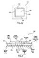
- FIG. 2Ashows a top view of a stiffener.
- FIG. 2Bshows a temperature distribution for a stiffener during operation of an IC device in a flex BGA package.
- FIG. 2Cshows an top view of an alternative stiffener configuration.
- FIG. 3shows a cross-sectional view of a conventional die-up plastic BGA package.
- FIG. 4illustrates a cross-sectional view of a die-up flex BGA package with heat spreader, according to an embodiment of the present invention.
- FIG. 5show a cross-sectional view of an alternative BGA package, according to embodiments of the present invention, where the heat spreader is internal to the BGA package.
- FIG. 6illustrates a cross-sectional view of a die-up flex BGA package with stiffener ground plane, according to an embodiment of the present invention.
- FIG. 7illustrates a cross-sectional view of a die-up flex BGA package with patterned stiffener, according to an embodiment of the present invention.
- FIG. 8illustrates a cross-sectional view of a die-up flex BGA package with ground/thermal connector, according to an embodiment of the present invention.
- FIG. 9Aillustrates a cross-sectional view of a die-up tape BGA package with metal ring, according to an embodiment of the present invention.
- FIG. 9Billustrates a top view of the die-up tape BGA package with metal ring of FIG. 9A, according to an embodiment of the present invention.
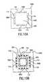
- FIG. 10Aillustrates a stiffener that includes one or more thermal studs, according to an embodiment of the present invention.
- FIG. 10Billustrates an IC die that is wire bound to a substrate through openings in the stiffener of FIG. 10A, according to an embodiment of the present invention.
- FIG. 11illustrates a cross-sectional view of a die-up PBGA package with ground/thermal connector, according to an embodiment of the present invention.
- FIG. 12Aillustrates a cross-sectional view of a die-up BGA package.
- FIGS. 12B and 12Cillustrate exemplary solder ball arrangements-for the die-up BGA package of FIG. 12A.
- FIG. 13shows exemplary routing in a substrate layer.
- FIG. 14shows a flowchart related to FIGS. 4 and 5, that provides operational steps of exemplary embodiments of the present invention.
- FIG. 15shows a flowchart related to FIG. 6 that provides operational steps of exemplary embodiments of the present invention.
- FIGS. 16 A-Dshow flowcharts related to FIGS. 7 and 8 that provide operational steps of exemplary embodiments of the present invention.
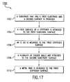
- FIG. 17shows a flowchart related to FIGS. 9A and 9B that provides operational steps of exemplary embodiments of the present invention.
- FIG. 18shows a flowchart related to FIGS. 10A and 10B that provides operational steps of exemplary embodiments of the present invention.
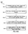
- FIGS. 19 A-Cshow flowcharts related to FIG. 11 that provide operational steps of exemplary embodiments of the present invention.
- FIG. 20illustrates a substrate that has a central window opening, according to an embodiment of the present invention.
- FIG. 21illustrates a side view of a stiffener that has a downward protruding portion, according to an embodiment of the present invention.
- the present inventionis directed to a method and system for improving the mechanical, thermal, and electrical performance of BGA packages.
- the present inventionis applicable to all types of BGA substrates, including ceramic, plastic, and tape (flex) BGA packages. Furthermore the present invention is applicable to die-up (cavity-up) and die-down (cavity-down) orientations.
- BGA package thermal stress at the IC die/stiffener interfaceis released or altered with the introduction of a heat spreader on the top surface of the IC die, enabling large size dies with high input and output (I/O) counts to be packaged using BGA technology.
- BGA package thermal resistance and the length of the current return pathare reduced by introducing thermal/ground balls underneath or within close proximity of the IC die.
- the package thermal resistance and ground inductanceare reduced by removing center solder balls, and enabling the attachment of a die pad to the PCB.
- the die padis attached to the PCB with novel patternings of the metal stiffener, or by positioning a thermal/ground connector in between the IC die pad and the PCB.
- the package thermal resistanceis reduced by attaching a metal ring to the top surface of a stiffener.
- the package thermal resistanceis reduced by bridging the die pad to the outer regions of the stiffener with metal studs.
- the electrical performance of the BGA packageis improved.
- electrical performanceis improved by connecting ground bonds from the IC die to the stiffener.
- the stiffeneroperates as a package ground plane.
- the package ground planemay be connected to PCB ground through either thermal/ground balls or thermal/ground connectors mentioned in embodiments above, and further described herein.
- package power distributionis enhanced by using a layer in a tape substrate as a power or ground plane.
- plastic ball grid array (PBGA) package thermal and electrical performancesare improved.
- PBGAplastic ball grid array
- Ball grid array package typesare described below. Further detail on the above described embodiments, and additional embodiments according to the present invention, are presented below. The embodiments described herein may be combined in any applicable manner, as required by a particular application.
- a ball grid array (BGA) packageis used to package and interface an IC die with a printed circuit board (PCB).
- BGA packagesmay be used with any type of IC die, and are particularly useful for high speed ICs.
- solder padsdo not just surround the package periphery, as in chip carrier type packages, but cover the entire bottom package surface in an array configuration.
- BGA packagesare also referred to as pad array carrier (PAC), pad array, land grid array, and pad-grid array packages.
- PACpad array carrier
- BGA packages typesare further described in the following paragraphs. For additional description on BGA packages, refer to Lau, J. H., Ball Grid Array Technology , McGraw-Hill, New York, (1995), which is herein incorporated by reference in its entirety.
- die-up and die-down BGA package configurationsexist.
- the IC dieis mounted on a top surface of the substrate or stiffener, in a direction away from the PCB.
- die-down BGA packagesthe IC die is mounted on a bottom surface of the substrate or stiffener, in a direction towards the PCB.
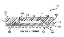
- FIG. 1Aillustrates a conventional flex BGA package 100 .
- Flex BGA package 100includes an IC die 102 , a tape substrate 104 , a plurality of solder balls 106 , and one or more wire bonds 108 .
- Tape or flex BGA packagesare particularly appropriate for large IC dies with large numbers of input and outputs, such as application specific integrated circuits (ASIC) and microprocessors.
- ASICapplication specific integrated circuits
- Tape substrate 104is generally made from one or more conductive layers bonded with a dielectric material.
- the dielectric materialmay be made from various substances, such as polyimide tape.
- the conductive layersare typically made from a metal, or combination of metals, such as copper and aluminum. Trace or routing patterns are made in the conductive layer material.
- Substrate 104may be a single-layer tape, a two-layer tape, or additional layer tape substrate type. In a two-layer tape, the metal layers sandwich the dielectric layer, such as in a copper-Upilex-copper arrangement.
- IC die 102is attached directly to substrate 104 , for example, by an epoxy.
- IC die 102is any type of semiconductor integrated circuit, separated from a semiconductor wafer.
- One or more wire bonds 108connect corresponding bond pads 118 on IC die 102 to contact points 120 on substrate 104 .
- An encapsulate, mold compound, or epoxy 116covers IC die 102 and wire bonds 108 for mechanical and environmental protection.
- flex BGA package 100does not include a stiffener.
- a stiffenercan be attached to the substrate to add planarity and rigidity to the package.
- FIG. 1Billustrates a flex BGA package 110 , similar to flex BGA package 100 , that incorporates a stiffener 112 .
- Stiffener 112may be laminated to substrate 104 .
- Stiffener 112is typically made from a metal, or combination of metals, such as copper, tin, and aluminum, or may be made from a polymer, for example.
- Stiffener 112also may act as a heat sink, and allow for greater heat spreading in BGA package 110 .
- One or more openings 114 in stiffener 112may be used to allow for wire bonds 108 to connect IC die 102 to substrate 104 .
- Stiffener 112may be configured in other ways, and have different opening arrangements than shown in FIG. 1B.
- FIG. 2Ashows a top view of a stiffener 112 .
- Stiffener 112includes an opening 114 adjacent to all four sides of an IC die mounting position 202 in the center of stiffener 112 .
- FIG. 2Bshows a temperature distribution 204 of a stiffener, such as stiffener 112 , during operation of an IC die in a flex BGA package. Temperature distribution 204 shows that heat transfer from IC die mounting position 202 to the edges of stiffener 112 is substantially limited by openings 114 . Openings 114 act as thermal barriers to heat spreading in stiffener 112 .
- FIG. 2Cshows a top view of an alternative configuration for stiffener 112 , according to an embodiment of the present invention.
- Stiffener 112includes an opening 206 adjacent to all four sides of an IC die mounting position 202 in the center of stiffener 112 . Openings 206 are similar to openings 114 of FIG. 2A, but of different shape. Further alternatively shaped openings in stiffener 112 are applicable to the present invention.
- FIG. 3shows a cross-sectional view of a conventional die-up PBGA package 300 .
- PBGA package 300includes a plastic substrate 302 , an IC die 304 , a plurality of solder balls 306 , a plurality of wire bonds 308 , a die pad 310 , one or more vias 314 , and one or more thermal/ground vias 316 .
- Plastic substrate 302includes one or more metal layers formed on an organic substrate (for example, BT resin or FR 4 epoxy/glass).
- IC die 304is mounted to die pad 310 .
- IC die 304may be attached to die pad 310 with an epoxy, such as a silver-filled epoxy.
- Wire bonds 308connect signals of IC die 304 to substrate 302 .
- gold bonding wireis bonded from aluminum bond pads on IC die 304 to gold-plated contact pads on substrate 302 .
- the contact pads on substrate 302connect to solder balls 306 attached to the bottom surface of substrate 302 , through vias 314 and routing within substrate 302 using copper conductors 312 .
- Thermal/ground vias 316connect die pad 310 to one or more thermal/ground balls 322 on the center bottom surface of substrate 302 .
- An encapsulate, mold compound, or epoxy 320covers IC die 304 and wire bonds 308 for mechanical and environmental protection.
- a BGA packageincludes an array of solder balls located on a bottom external surface of the package substrate.
- FIG. 12Aillustrates a cross-sectional view of a die-up BGA package 1200 .
- FIGS. 12B and 12Cillustrate exemplary solder ball arrangements for die-up BGA package 1200 .
- BGA package 1200includes an IC die 1208 mounted on a substrate 1212 .
- IC die 1208is electrically connected to substrate 1212 by one or more wire bonds 1210 .
- Wire bonds 1210are electrically connected to solder balls 1206 underneath substrate 1212 through corresponding vias and routing in substrate 1212 .
- the vias in substrate 1212can be filled with a conductive material, such as solder, to allow for these connections.
- Solder balls 1206are attached to substrate 1212 , and are used to attach the BGA package to a PCB.
- wire bondssuch as wire bonds 1210
- IC diesmay be mounted and coupled to a substrate with solder balls located on the bottom surface of the IC die, by a process commonly referred to as “C4” or “flip chip” packaging.
- solder balls 1206may be arranged in an array.
- FIG. 12Bshows a 14 by 14 array of solder balls on the bottom surface of BGA package 1200 .
- Other sized arrays of solder ballsare also applicable to the present invention.
- Solder balls 1206are reflowed to attach BGA package 1200 to a PCB.
- the PCBmay include contact pads to which solder balls 1206 are bonded.
- PCB contact padsare generally made from a metal or combination of metals, such as copper, nickel, tin, and gold.
- FIG. 12Cshows a bottom view of BGA package 1200 , with an alternative solder ball array arrangement.
- BGA package 1200attaches an array of solder balls 1206 on a bottom surface of substrate 1212 .
- solder balls 1206are located in a peripheral area of the bottom surface of substrate 1212 , away from a substrate center 1224 .
- solder balls 1206 on the bottom surface of substrate 1212may be located outside an outer profile area of an IC die mounted on the opposite surface of substrate 1212 .
- the solder ball arraymay be organized in any number of ways, according to the requirements of the particular BGA package application.
- solder ball arrangement shown in FIG. 12Cis particularly applicable to embodiments of the present invention described below, such as for attaching a heat spreader or ground/thermal connector to a bottom surface of a BGA package.
- the heat spreader or ground/thermal connectormay be connected in substrate center 1224 .
- the BGA package substrateprovides vias and routing on one or more layers to connect contact pads for wire bonds on its upper surface to solder balls attached to the bottom substrate surface.
- FIG. 13shows an example routing 1304 in a substrate layer 1302 for accomplishing this.
- the present inventionis applicable to improving thermal and electrical performance in the BGA package types described herein, and further BGA package types.
- a heat spreadermay be used in a BGA package to provide for thermal stress relief and heat dissipation.
- a drop-in heat spreaderis attached to the top surface of an IC die in a flex BOA package to provide for thermal stress relief and heat dissipation.
- FIG. 4illustrates a cross-sectional view of a die-up flex BGA package 400 , according to an embodiment of the present invention.
- BGA package 400includes IC die 102 , substrate 104 , plurality of solder balls 106 , one or more wire bonds 108 , stiffener 112 , epoxy 116 , a drop-in heat spreader 402 , and an epoxy 404 . Refer to the discussion above related to FIGS. 1 A- 1 B for additional detail on the structure and operation of some of these elements.
- Substrate 104has a top surface to which a bottom surface of stiffener 112 is mounted. A bottom surface of substrate 104 attaches the plurality of solder balls 106 . The plurality of solder balls 106 connect to vias and/or points on the bottom surface of substrate 104 to which signals internal to substrate 104 are routed and exposed.
- Stiffener 112has a top surface to which IC die 102 is mounted.
- BGA package 400does not require a stiffener, and does not include a stiffener 112 .
- IC die 102is mounted to substrate 104 .
- One or more wire bonds 108connect corresponding bond pads 118 on IC die 102 to contact points 120 on substrate 104 .
- wire bonds 108extend through one or more openings 114 in stiffener 112 to form connections with substrate 104 .
- Heat spreader 402is attached to the top surface (active surface) of IC die 102 using epoxy 404 .
- the epoxy 404may be the same substance as epoxy 116 , or may be a different substance.
- Silver filled epoxiesmay be used for epoxy 404 to enhance heat extraction from IC die 102 .
- heat spreader 402is smaller in area than the upper surface of IC die 102 .
- Alternative sizes for heat spreader 402are also applicable to the present invention, including sizes equal to the area of IC die 102 , or larger areas.
- Heat spreader 402is shaped and configured to spread heat from IC die 102 , as is required by the application.
- FIG. 4show a cross-sectional view of an alternative BGA package 500 , according to embodiments of the present invention, where a heat spreader 502 is internal to BGA package 500 . Heat spreader 502 is completely encapsulated by epoxy 116 .
- the mechanical structure of BGA package 400becomes more symmetrical in its center region, particularly when ground/thermal solder balls do not exist on the bottom surface of substrate 104 underneath the outer profile of IC die 102 .
- Thermal stress at the interface of IC die 102 and stiffener 112is substantially released or altered by heat spreader 402 .
- Deformation caused by thermal stress in stiffener 112 and substrate 104is substantially reduced through the use of heat spreader 402 .
- Drop-in heat spreader 402allows for even larger sizes for IC die 102 and greater I/O counts by providing for greater heat spreading capacity in BGA package 400 .
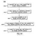
- FIG. 14shows a flowchart 1400 providing operational steps for assembling one or more embodiments of the present invention.
- the steps of FIG. 14do not necessarily have to occur in the order shown, as will be apparent to persons skilled in the relevant art(s) based on the teachings herein.
- Other structural embodimentswill be apparent to persons skilled in the relevant art(s) based on the following discussion. These steps are described in detail below.
- Flowchart 1400begins with step 1402 .
- a substratethat has a first surface and a second surface is provided.
- the substrateis flex substrate 104 , or another substrate type suitable for a BGA package.
- an IC die mounting position and/or contact pointsare provided on a first, upper surface, and solder ball pads are provided on a second, bottom surface.
- a first surface of a stiffeneris attached to the first substrate surface.
- the stiffeneris stiffener 112 , which is attached to substrate 104 .
- a stiffeneris not required.
- an IC dieis mounted to the second stiffener surface.
- the IC dieis IC die 102 , which is mounted to stiffener 112 .
- IC die 102is mounted directly to the substrate.
- a heat spreaderis mounted to the IC die, wherein the heat spreader dissipates heat from the IC die.
- the heat spreaderis heat spreader 402 or 502 , which is mounted with epoxy 404 or other attachment means to the upper surface of IC die 102 .
- Heat spreader 402 or 502typically is mounted to the center of the upper surface of IC die 102 , and covers less than the entire upper surface of IC die 102 .
- the smaller area of heat spreader 402 or 502allows for bond pads 118 to be exposed on the upper surface of IC die 102 for wire bond connections.
- heat spreader 402 or 502is of the same size, or comprises a larger area than the upper surface of IC die 102 .
- a plurality of solder ballsare attached to the second substrate surface.
- the plurality of solder ballsare plurality of solder balls 106 , which connect to vias and/or solder ball pads on the bottom surface of substrate 104 .
- the solder ballsmay be arranged on the bottom surface of substrate 104 as shown in FIGS. 12B and 12C, or in alternative arrangements.
- the solder ballsare used to attach a BGA package to a PCB.
- a benefit of performing the steps of flowchart 1400is that the heat spreader relieves thermal stress at an interface of the IC die and the first stiffener surface.
- Flowchart 1400may include the additional step where the second stiffener surface is encapsulated.
- the second stiffener surfacemay be encapsulated by a resin or molding compound, that also encapsulates the IC die, heat spreader, and wire bonding.
- electrical performance of an IC die, and thermal performance of a corresponding BGA packagemay be improved by allowing a stiffener to act as a ground plane.
- a stiffener in a die-up tape BGA (Flex BGA) packageis coupled to PCB ground through one or more vias to ground solder balls.
- Ground contact pads of the IC dieare connected to the stiffener by ground wire bonds.
- one or more metal layers of a flex tape substratemay be coupled to a ground or power potential, to operate as a ground or power plane.
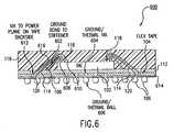
- FIG. 6illustrates a cross-sectional view of a die-up flex BGA package 600 , according to an embodiment of the present invention.
- BGA package 600includes IC die 102 , substrate 104 , plurality of solder balls 106 , one or more wire bonds 108 , stiffener 112 , epoxy 116 , one or more ground bonds to stiffener 602 , one or more ground/thermal vias 604 , one or more ground/thermal balls 606 , one or more ground contact pads 608 , one or more power contact pads 610 , and one or more power vias 612 .
- Substrate 104has a top surface to which a bottom surface of stiffener 112 is mounted. A bottom surface of substrate 104 attaches the plurality of solder balls 106 . The plurality of solder balls 106 connect to vias and/or points on the bottom surface of substrate 104 to which signals internal to substrate 104 are routed and exposed.
- Stiffener 112has a top surface to which IC die 102 is mounted.
- One or more wire bonds 108connect corresponding bond pads 118 on IC die 102 to contact points 120 on substrate 104 .
- Wire bonds 108extend through one or more openings 114 in stiffener 112 to form connections with substrate 104 .
- IC die 102has a top surface that includes at least one ground pad 608 .
- Ground pad 608is coupled to a ground potential signal in IC die 102 .
- a ground wire bond 602connects ground pad 608 to stiffener 112 .
- the bottom surface of stiffener 112is coupled to a ground potential signal in the PCB to which BGA package 600 is attached, to cause stiffener 112 to operate as a ground plane.
- Stiffener 112is coupled to PCB ground through one or more of ground/thermal via 604 that extend through substrate 104 .
- the one or more of ground/thermal vias 604are located in substrate 104 , underneath IC die 102 , and can be filled with a conductive material, such as solder.
- a ground/thermal solder ball 606is attached to each ground/thermal via 604 on the bottom surface of substrate 104 .
- Ground/thermal solder ball 606forms the connection to PCB ground, when reflowed to attach to the PCB.
- Each ground/thermal via 604connects the respective ground/thermal solder ball 606 to stiffener 112 both electrically and thermally.
- a tape substrateis configured such that a metal layer is used as a package power or ground plane.
- a metal layeris used as a package power or ground plane.
- the bottom metal layermay be used as a power or ground plane.
- PCB package 600includes a bottom metal layer 614 of a two-layer tape substrate 104 that is coupled to a potential to operate as a power plane, according to an embodiment of the present invention.
- One or more power contact pads 610 on IC die 102are coupled to a power potential signal in IC die 102 .
- Power contact pad 610 on IC die 102is connected to a corresponding power via 612 by a power wire bond 616 .
- power wire bond 616extends through opening 114 .
- Power via 612extends through substrate 104 .
- Power via 612can be filled with a conductive material, such as solder.
- Each power via 612is coupled to the bottom metal layer 614 of substrate 104 .
- one or more power vias 612may be connected to corresponding solder balls on the bottom of substrate 104 , to connect bottom metal layer 614 to PCB power pads when the solder balls are reflowed.
- thermal vias in a flex tape substrateand of the use of a thermal ball coupled to a heat spreader in a die-down TBGA package, refer to U.S. Pat. No. 6,020,637, which is incorporated by reference in its entirety herein.
- thermal via and a thermal ball in a plastic substrate BGA packagerefer to U.S. Pat. No. 5,894,410, which is incorporated by reference in its entirety.
- FIG. 15shows a flowchart 1500 providing operational steps for assembling one or more embodiments of the present invention.
- the steps of FIG. 15do not necessarily have to occur in the order shown, as will be apparent to persons skilled in the relevant art(s) based on the teachings herein.
- Other structural embodimentswill be apparent to persons skilled in the relevant art(s) based on the following discussion. These steps are described in detail below.
- Flowchart 1500begins with step 1502 .
- a substratethat has a first surface and a second surface is provided.
- the substrateis flex substrate 104 , or another substrate type suitable for a BGA package.
- an IC die mounting position and/or contact pointsare provided on a first, upper surface, and solder ball pads are provided on a second, bottom surface.
- step 1504at least one opening in a stiffener from a first surface of the stiffener to a second surface of the stiffener is provided.
- the at least one openingincludes openings 114 in stiffener 112 .
- an opening 114is located on each of the four edges of IC die 102 .
- the first stiffener surfaceis attached to the first substrate surface.
- the stiffeneris stiffener 112 , which is attached to substrate 104 .
- a stiffeneris not required, and is not attached to the substrate.
- an integrated circuit (IC) dieis mounted to the second stiffener surface, wherein a first surface of the IC die includes a contact pad.
- the IC dieis IC die 102 , which is mounted to stiffener 112 .
- IC die 102is mounted directly to the substrate.
- the contact padis ground contact pad 608 .
- the contact padis coupled to the second stiffener surface.
- contact padis ground contact pad 608 , which is connected to stiffener 112 by ground wire bond 602 .
- Ground wire bond 602may be soldered, or otherwise attached to stiffener 112 .
- a plurality of solder ballsis attached to the second substrate surface, inside an outer dimensional profile of the IC die.
- the plurality of solder ballsinclude one or more ground/thermal balls 606 , which are arranged on the bottom surface of substrate 104 in the region of substrate center 1224 , shown in FIG. 12C.
- the outer dimensional profile of the IC dieis the area bounded by the edges of IC die 102 .
- the plurality of solder ballsare coupled through corresponding vias in the substrate to the first stiffener surface.
- the viasinclude ground/thermal via 604 .
- the viascan be filled with a conductive material, such as solder, to allow the electrical connection of the solder balls to stiffener 112 .
- the substrateincludes a metal layer, wherein the metal layer is coupled to a second potential.
- the stiffenerhas at least one opening extending from the first stiffener surface to the second stiffener surface.
- the second IC die surfaceincludes a second contact pad.
- the second contact padis coupled to the metal layer through one of the openings in the stiffener and through a corresponding via that extends through the substrate.
- the second contact padmay be coupled to a power or ground potential in the IC die.
- the second contact padis power contact pad 610
- the metal layeris metal layer 614
- the corresponding viais power via 612 .
- flowchart 1500may include an additional step, where the contact pad is coupled to a ground potential in the IC die.
- the contact padmay be connected to a ground plane or ground signal in IC die that is routed to the contact pad.
- Flowchart 1500may include the additional step where the second stiffener surface is encapsulated.
- the second stiffener surfacemay be encapsulated by a resin or molding compound, that also encapsulates the IC die and wire bonding.
- Flowchart 1500may include the additional step where a second plurality of solder balls is attached to the second substrate surface, outside an outer dimensional profile of the IC die.
- the second plurality of solder ballsare plurality of solder balls 106 , which connect to vias and/or solder ball pads on the bottom surface of substrate 104 .
- the solder ballsare arranged on the bottom surface of substrate 104 as shown in FIG. 12B, outside of substrate center 1224 .
- the solder ballsare used to attach a BGA package to a PCB.
- electrical performance of the IC device, and thermal performance of a BGA packageis improved by enabling an IC die pad to attach to a PCB.
- the IC die padis attached to the PCB by a novel patterning of the metal stiffener in a die-up tape BGA package.
- the IC die padis attached to the PCB by placing a thermal/ground connector between the IC die pad and PCB in a die-up tape BGA package.
- a BGA package junction-to-board thermal resistancecan be substantially reduced by the attachment of a metal die-attach pad directly to a PCB.
- Metal die-attach padsare coupled to a PCB for package junction-to-board thermal resistance minimization in an exposed pad quad flat pack (QFP), a QFP with exposed heat sink at bottom, and a leadless plastic chip carrier (i.e. LPCC, QFN, SON, QLP) package, for instance.
- QFPexposed pad quad flat pack
- QFPQFP with exposed heat sink at bottom
- a leadless plastic chip carrieri.e. LPCC, QFN, SON, QLP
- All existing such designs that involve an exposed die pad or an exposed heat sink at package bottomare “lead frame” packages.
- the present inventionprovides for an exposed die-attach pad or heat sink at the bottom of flex BGA packages.
- FIG. 7illustrates a cross-sectional view of a die-up flex BGA package 700 , according to an embodiment of the present invention.
- BGA package 700includes IC die 102 , substrate 104 , plurality of solder balls 106 , one or more wire bonds 108 , stiffener 112 , epoxy 116 , ground wire bond to stiffener 602 , ground contact pad 608 , and a stiffener cavity 702 .
- Substrate 104has a top surface to which a bottom surface of stiffener 112 is mounted. A bottom surface of substrate 104 attaches the plurality of solder balls 106 . The plurality of solder balls 106 connect to vias and/or points on the bottom surface of substrate 104 to which signals internal to substrate 104 are routed and exposed. Substrate 104 in FIG. 7 has a central window-shaped opening 704 , under which solder balls are preferably not connected.
- FIG. 20illustrates a bottom view of a substrate 104 that has a central window opening 704 , according to an embodiment of the present invention.
- Stiffener 112has a top surface to which IC die 102 is mounted. Stiffener 112 in FIG. 7 is patterned with a cavity 702 , which protrudes downward for attachment of IC die 102 . As described above, a central window-shaped opening 704 exists in substrate 104 . This opening 704 exists to allow stiffener 112 to protrude through, and make contact with soldering pads on a PCB to which BGA package 700 is to be mounted. The bottom exposed surface of cavity 702 can be plated with solder to facilitate surface mount to solder plated metal pads on a PCB to which BGA package 700 is mounted. Hence, stiffener 112 may act as a conduit for heat to be transferred from IC die 102 to the PCB.
- Stiffener 112may optionally be configured to operate as a ground plane.
- One or more ground pads 608may be coupled to a ground potential signal in IC die 102 .
- a ground wire bond 602connects each ground pad 608 to stiffener 112 .
- the bottom exposed surface of cavity 702may function both as an exposed ground pad of BGA package 700 , and as an exposed heat spreader.
- the bottom exposed surface of cavity 702may be plated with solder to allows stiffener 112 to be surface mounted to one or more soldering pads on the PCB.
- the pads on the PCBcan be connected to a PCB ground plane to shorten the length of electrical current return paths, as well as to form a conductive heat dissipation path from BGA package 700 to the PCB.
- FIG. 8illustrates a cross-sectional view of a die-up flex BGA package 700 , according to an embodiment of the present invention.
- Substrate 104 in FIG. 8has a central window-shaped opening, under which no solder balls are connected.
- a portion of the bottom surface of stiffener 112is exposed through the central window-shaped opening 704 of substrate 104 .
- a heat spreader(for example, manufactured from copper or aluminum), shown as ground/thermal connector 802 , is coupled to the exposed portion of stiffener 112 .
- Ground/thermal connector 802can be made from the same material as stiffener 112 . Material different from stiffener 112 may be used for ground/thermal connector 802 to compensate for the mismatch of thermal expansion coefficient between the die 102 and stiffener 112 .
- Ground/thermal connector 802may be laminated to the exposed portion of stiffener 112 using conductive epoxy.
- the bottom surface of ground/thermal connector 802may be plated with solder to facilitate its surface mount to soldering pads on the PCB.
- Metal pads on the PCBmay be connected to a PCB ground plane to shorten the length of electrical current return paths, as well as enhance the conductive heat dissipation path from IC die 102 to the PCB.
- stiffener 112 and ground/thermal connector 802may be manufactured from a single piece of metal, and hence consist of a single metal piece.
- FIG. 21illustrates a side view of stiffener 112 that has a downward protruding portion 2102 , according to an embodiment of the present invention.
- portion 2102extends partially or entirely through window-shaped opening 704 .
- Portion 2102may be directly connected to the PCB, or may be connected to a ground/thermal connector 802 that is connected to the PCB. Because of the thermal and electrical improvement enabled by the coupling of stiffener 112 to a PCB, length of wire bonds can be reduced by moving opening 114 closer to the proximity of die 102 without compromising thermal performance significantly.
- FIG. 16Ashows a flowchart 1600 providing operational steps for assembling one or more embodiments of the present invention.
- FIGS. 16 B-Dprovide operational steps according to further embodiments. The steps of FIGS. 16 A-D do not necessarily have to occur in the order shown, as will be apparent to persons skilled in the relevant art(s) based on the teachings herein. Other structural embodiments will be apparent to persons skilled in the relevant art(s) based on the following discussion. These steps are described in detail below.
- Flowchart 1600begins with step 1602 .
- a substratethat has a first surface and a second surface is provided.
- the substrateis flex substrate 104 , or another substrate type suitable for a BGA package.
- an IC die mounting position and/or contact pointsare provided on a first, upper surface, and solder ball pads are provided on a second, bottom surface.
- a first surface of a stiffeneris attached to the first substrate surface.
- the stiffeneris stiffener 112 , which is attached to substrate 104 .
- step 1606a portion of the first stiffener surface is exposed through a window opening in the substrate.
- substrate 104has a window opening 704 in its center.
- a portion of the bottom surface of stiffener 112is exposed through window opening 704 .
- an IC dieis mounted to a second surface of the stiffener, wherein a surface of the IC die includes at least one contact pad.
- the IC dieis IC die 102 , which is mounted to stiffener 112 .
- a plurality of solder ballsare attached to the second substrate surface.
- the plurality of solder ballsare plurality of solder balls 106 , which connect to vias and/or solder ball pads on the bottom surface of substrate 104 .
- the solder ballsare arranged on the bottom surface of substrate 104 as shown in FIG. 12B, exclusive of the area of window opening 704 .
- the solder ballsare used to attach a BGA package to a PCB.
- step 1612the exposed portion of the first stiffener surface is configured to be coupled to a printed circuit board (PCB), whereby electrical and thermal performance of the BGA package is improved.
- PCBprinted circuit board
- FIG. 16Bprovides exemplary steps for performing step 1612 :
- a heat spreaderis coupled to the exposed portion of the first stiffener surface.
- the heat spreaderis ground/thermal connector 802 , which is coupled to stiffener 112 through window opening 702 .
- step 1616a surface of the heat spreader is configured to be coupled to the PCB.
- step 1612further includes the step where the heat spreader surface is plated with solder to allow the heat spreader surface to be surface mounted to soldering pads on the PCB.
- step 1612comprises the step where the stiffener is shaped to have a centrally-located cavity shaped portion that protrudes through the window opening.
- step 1612further includes the step where a surface of the cavity shaped portion is plated with solder to allow the stiffener to be surface mounted to soldering pads on the PCB.
- stiffener 112is patterned with a cavity 702 , which protrudes downward in window opening 704 .
- the bottom surface of cavity 702is plated with solder.
- FIG. 16Cprovides additional exemplary steps for flowchart 1600 of FIG. 16A:
- the stiffeneris coupled to a potential.
- the stiffenermay be coupled to ground or power on the PCB.
- the bottom surface of cavity 702may be coupled to the ground or power potential on the PCB, or ground/thermal connector 802 may make the connection to the PCB.
- each of the at least one contact padsare coupled to the second stiffener surface with corresponding wire bonds.
- FIG. 16Dprovides exemplary steps for performing step 1618 :
- step 1622the stiffener is coupled to a ground potential.
- step 1624the stiffener allowed to serve as a ground plane.
- Flowchart 1600may include the additional step where the second stiffener surface is encapsulated.
- the second stiffener surfacemay be encapsulated by an epoxy, that also encapsulates the IC die and wire bonding.
- the mechanical and thermal performance of a BGA packageis enhanced by attaching a metal ring to the top surface of the stiffener.
- a metal ringis attached to the top surface of the stiffener in a die-up tape BGA package.
- FIG. 9Aillustrates a cross-sectional view of a die-up tape BGA package 900 , according to an embodiment of the present invention.
- BGA package 900includes IC die 102 , substrate 104 , plurality of solder balls 106 , one or more wire bonds 108 , stiffener 112 , epoxy 116 , and a ring 902 .
- FIG. 9Billustrates a top view of die-up tape BGA package 900 , with ring 902 .
- Substrate 104has a top surface to which a bottom surface of stiffener 112 is mounted. A bottom surface of substrate 104 attaches the plurality of solder balls 106 . The plurality of solder balls 106 connect to vias and/or points on the bottom surface of substrate 104 to which signals internal to substrate 104 are routed and exposed.
- One or more wire bonds 108connect corresponding bond pads 118 on IC die 102 to contact points 120 on substrate 104 .
- Wire bonds 108extend through one or more openings 114 in stiffener 112 to form connections with substrate 104 .
- Stiffener 112has a top surface to which IC die 102 is mounted. Furthermore, ring 902 is attached to the top surface of stiffener 112 . Ring 902 may be laminated to stiffener 112 , after wire bonding is completed. Epoxy 116 is filled in and flushed to ring 902 after the attachment of ring 902 .
- Ring 902is preferably made of a metal, such as copper or aluminum, or a combination thereof, but may be constructed from other applicable materials. Preferably, ring 902 is made from the same material as stiffener 112 , to minimize the mismatch of the thermal expansion coefficient. Ring 902 is preferably flush with the outer edges of stiffener 112 to form an outer edge of BGA package 900 , but may also reside entirely within an outer profile of stiffener 112 .
- a primary benefit of attaching ring 902 to stiffener 112is an increase in stiffness of BGA package 900 .
- Ring 902also aids in reducing the amount of warp of BGA package 900 .
- ring 902promotes heat dissipation from stiffener 112 , reduces junction-to-case thermal resistance, and facilitates the attachment of an external heat spreader to BGA package 900 .
- ring 902enhances the process of encapsulation of the BGA package. Ring 902 , with stiffener 112 , creates a cavity that may be filled with a dispensed glob top or encapsulating material, that locks IC die 102 and surrounding elements in place.
- FIG. 17shows a flowchart 1700 providing operational steps for assembling one or more embodiments of the present invention.
- the steps of FIG. 17do not necessarily have to occur in the order shown, as will be apparent to persons skilled in the relevant art(s) based on the teachings herein.
- Other structural embodimentswill be apparent to persons skilled in the relevant art(s) based on the following discussion. These steps are described in detail below.
- Flowchart 1700begins with step 1702 .
- a substratethat has a first surface and a second surface is provided.
- the substrateis flex substrate 104 , or another substrate type suitable for a BGA package.
- an IC die mounting position and/or contact pointsare provided on a first, upper surface, and solder ball pads are provided on a second, bottom surface.
- a first surface of a stiffeneris attached to the first substrate surface.
- the stiffeneris stiffener 112 , which is attached to substrate 104 .
- a stiffeneris not required, and is not attached to the substrate.
- an IC dieis mounted to the first stiffener surface.
- the IC dieis IC die 102 , which is mounted to stiffener 112 .
- IC die 102is mounted directly to the substrate.
- a plurality of solder ballsare attached to the second substrate surface.
- the plurality of solder ballsare plurality of solder balls 106 , which connect to vias and/or solder ball pads on the bottom surface of substrate 104 .
- the solder ballsmay be arranged on the bottom surface of substrate 104 as shown in FIGS. 12B and 1 2 C, or in alternative arrangements.
- the solder ballsare used to attach a BGA package to a PCB.
- a metal ringis attached to the first stiffener surface. Attaching the metal ring enhances heat dissipation from the stiffener.
- the metal ringis ring 902 .
- ring 902is attached directly to the substrate.
- Flowchart 1700may include the additional step where the second stiffener surface within the volume encompassed by the ring is encapsulated.
- a filled upper surfacemay be called a “glob top”.
- this volumemay be encapsulated by a resin or molding compound, that also encapsulates the IC die and wire bonding.
- the thermal performance of a BGA packageis improved by bridging an IC die pad to which the IC die is mounted to the outer regions of the stiffener.
- one or more metal studsare used as thermal bridges, to bridge the openings in the stiffener that surround the IC die, in a die-up tape BGA package.
- the openings on a stiffener surfaceallow for wire bond connections between an IC die and a substrate. These openings have the additional effect of reducing the amount of heat that can spread to the outer surface regions of the stiffener, hampering the ability of the stiffener to act as a heat spreader. This effect is illustrated in FIG. 2B, which is further described above.
- the stiffeneris patterned such that one or more short studs run across each wire bond opening. More than one stud may be used to bridge each wire bond opening to promote heat spreading.
- the manufacturing process used for lead frame patterningmay be adapted to pattern a stiffener with studs across the wire bond openings. The use of the studs, however, may reduce space for wire bonds, and may reduce BGA package I/O capability, in some situations.
- FIG. 10Aillustrates a stiffener 1000 , that includes one or more studs 1002 , according to an embodiment of the present invention.
- Stiffener 1000having one or more studs 1002 , may be incorporated into a BGA package in the same manner as is described elsewhere herein for stiffener 112 .
- a stud 1002bridges each opening 114 in stiffener 1000 .
- more than one stud 1002 per opening 114may be used.
- each opening 114may be bridged by a different number of studs 1002 . Some of openings 114 may be bridged by one or more studs 1002 , while other openings 114 may not be bridged at all.
- FIG. 10Bprovides an illustration where IC die 102 is wire bound to substrate 104 through stiffener 1000 , according to an embodiment of the present invention.
- One or more wire bonds 108connect corresponding bond pads 118 on IC die 102 to contact points 120 on substrate 104 .
- Wire bonds 108avoid studs 1002 when making connections to substrate 104 .
- FIG. 18shows a flowchart 1800 providing operational steps for assembling one or more embodiments of the present invention.
- the steps of FIG. 18do not necessarily have to occur in the order shown, as will be apparent to persons skilled in the relevant art(s) based on the teachings herein.
- Other structural embodimentswill be apparent to persons skilled in the relevant art(s) based on the following discussion. These steps are described in detail below.
- Flowchart 1800begins with step 1802 .
- a substratethat has a first surface and a second surface is provided.
- the substrateis flex substrate 104 , or another substrate type suitable for a BGA package.
- an IC die mounting position and/or contact pointsare provided on a first, upper surface, and solder ball pads are provided on a second, bottom surface.
- a wire bond openingis created along each edge of an IC die mount position on a stiffener, wherein each wire bond opening extends through the stiffener.
- the wire bond openingsare wire bond openings 114 in stiffener 1000 .
- the IC die mount positionis IC die mounting position 202 , shown in FIG. 10A.
- a first surface of the stiffeneris attached to the first substrate surface.
- the stiffeneris stiffener 1000 , which is attached to substrate 104 .
- an IC dieis mounted to a second surface of the stiffener.
- the IC dieis IC die 102 , which is mounted to stiffener 1000 , in IC die mounting position 202 .
- step 1810at least one of the wire bond openings are bridged with at least one stud.
- one or more of wire bond openings 114are bridged with one or more studs 1002 . Studs 1002 allow for increased heat spreading across corresponding wire bond openings 114 to the outer edges of stiffener 1000 .
- a plurality of solder ballsare attached to the second substrate surface.
- the plurality of solder ballsare plurality of solder balls 106 , which connect to vias and/or solder ball pads on the bottom surface of substrate 104 .
- the solder ballsmay be arranged on the bottom surface of substrate 104 as shown in FIGS. 12B and 12C, or in alternative arrangements.
- the solder ballsare used to attach a BGA package to a PCB.
- the flowchart 1800may include the further step where a contact pad on the IC die is coupled to the substrate with a wire bond, wherein the wire bond passes through one of the wire bond openings in the stiffener.
- Flowchart 1800may include the additional step where the second stiffener surface is encapsulated.
- the second stiffener surfacemay be encapsulated by a resin or molding compound, that also encapsulates the IC die and wire bonding.
- the electrical and thermal performance of a plastic BGA (PBGA) packageis improved by attaching a thermal/ground connector to the bottom surface of a PBGA package.
- the thermal/ground connectorcouples the bottom center of a plastic substrate of a die-up PBGA to the PCB. Heat from an IC die is more easily spread to the PCB through the thermal/ground connector, which is attached to the plastic substrate underneath the IC die.
- FIG. 11illustrates a cross-sectional view of a die-up PBGA package 1100 , according to an embodiment of the present invention.
- PBGA package 1100includes plastic substrate 302 , IC die 304 , plurality of solder balls 306 , plurality of wire bonds 308 , die pad 310 , one or more vias 314 , one or more thermal/ground vias 316 , epoxy 320 , a ground/thermal connector 1102 , epoxy 1104 , a plurality of ground bonds 1106 ,andaplurality of ground bond pads 1108 .
- IC die 304is mounted to die pad 310 .
- Wire bonds 308connect signals of IC die 304 to contact pads on substrate 302 .
- the contact pads on substrate 302connect to solder balls 306 attached to the bottom surface of substrate 302 , through vias 314 and routing within substrate 302 .
- Thermal/ground vias 316connect die pad 310 to an exposed metal plated plane 1110 at the bottom center of substrate 302 .
- die pad 310 and metal plated plane 1110may be exposed copper pads of plastic substrate 302 .
- Ground/thermal connector 1102is attached to metal plated plane 1110 .
- ground/thermal connector 1102may be a metal piece (copper or aluminum, for example) that is laminated to metal plated plane 1110 at the bottom center of substrate 302 using a conductive epoxy 1104 .
- a bottom surface 1112 of ground/thermal connector 1102may be plated with solder for surface mount to soldering pads on the PCB.
- BGA package 1100provides a thermal path of IC die 304 , to die pad 310 , to thermal/ground vias 316 , to metal plated plane 1110 , to epoxy 1104 , to ground thermal connector 1102 (and bottom surface 1112 ) to the PCB soldering pads. Heat spreading is improved by a direct thermal path from IC die 304 to the PCB.
- Metal pads on the PCBcan be connected to a PCB ground plane to advantageously shorten the length of electrical current return paths, as well shorten the conductive heat dissipation path from device junctions of IC die to the PCB.
- Ground bonds 1106may be used to couple ground bond pads 1108 on IC die 304 to die pad 310 , when die pad 310 is coupled to ground. This provides for very short ground connections for signals in IC die 304 .
- FIG. 19Ashows a flowchart 1900 providing operational steps for assembling one or more embodiments of the present invention.
- FIGS. 19 B-Cprovide operational steps according to further embodiments. The steps of FIGS. 19 A-C do not necessarily have to occur in the order shown, as will be apparent to persons skilled in the relevant art(s) based on the teachings herein. Other structural embodiments will be apparent to persons skilled in the relevant art(s) based on the following discussion. These steps are described in detail below.
- Flowchart 1900begins with step 1902 .
- a substratethat has a first surface and a second surface is provided.
- the substrateis plastic substrate 302 , or another substrate type suitable for a BGA package.
- an IC die mounting position and contact pointsare provided on a first, upper surface, and solder ball pads are provided on a second, bottom surface.
- an IC dieis mounted to the first substrate surface.
- the IC dieis IC die 304 , which is mounted to substrate 302 .
- IC die 304may be mounted to a die pad 310 attached to substrate 302 .
- a plurality of solder ballsare attached to the second substrate surface.
- the plurality of solder ballsare plurality of solder balls 306 , which connect to vias and/or solder ball pads on the bottom surface of substrate 302 .
- the solder ballsmay be arranged on the bottom surface of substrate 302 as shown in FIG. 12B, or in other arrangements.
- the solder ballsare used to attach a BGA package to a PCB.
- a first surface of a heat spreaderis coupled to the second substrate surface.
- the heat spreaderis ground/thermal connector 1102 , which is coupled to substrate 302 with epoxy 1104 .
- Ground/thermal connector 1102may be mounted to metal plated plane 1110 on substrate 302 by epoxy 1104 .
- a second surface of the heat spreaderis configured to be coupled to a printed circuit board (PCB).
- PCBprinted circuit board
- Second heat spreader surfaceis bottom surface 1112 .
- step 1910may include the step where the second surface of the heat spreader is plated with solder.
- Flowchart 1900may comprise the additional step where the first substrate surface is coupled to the heat spreader through at least one via that extends through the substrate.
- the first substrate surfacemay be coupled to the heat spreader by one or more ground/thermal vias 316 .
- FIG. 19Bprovides exemplary steps for performing step 1904 :
- a copper plated die-attach padis exposed in the center of the first substrate surface.
- the copper plated die-attach pad, die pad 310may be an exposed portion of a metal layer of plastic substrate 302 .
- step 1914the IC die is mounted to the copper plated die-attach pad.
- the IC diemay be mounted with an epoxy.
- FIG. 19Cprovides exemplary steps for performing step 1908 :
- a copper plated planeis exposed in the center of the second substrate surface.
- the copper plated plane, metal plated plane 1110is an exposed portion of a metal layer of plastic substrate 302 .
- step 1918the die-attach pad is coupled to the copper plated plane with the at least one via.
- Flowchart 1900may include the additional step where the first substrate surface is encapsulated.
- the first substrate surfacemay be encapsulated by a resin or molding compound, that also encapsulates the IC die and wire bonding.
Landscapes
- Engineering & Computer Science (AREA)
- Computer Hardware Design (AREA)
- Microelectronics & Electronic Packaging (AREA)
- Power Engineering (AREA)
- Physics & Mathematics (AREA)
- Condensed Matter Physics & Semiconductors (AREA)
- General Physics & Mathematics (AREA)
- Chemical & Material Sciences (AREA)
- Materials Engineering (AREA)
- Geometry (AREA)
- Ceramic Engineering (AREA)
- Cooling Or The Like Of Semiconductors Or Solid State Devices (AREA)
Abstract
Description
- 1. Field of the Invention[0001]
- The invention relates generally to the field of integrated circuit (IC) device packaging technology, and more particularly to substrate stiffening and heat spreading techniques in ball grid array (BGA) packages.[0002]
- 2. Related Art[0003]
- Integrated circuit (IC) dies are typically mounted in or on a package that is attached to a printed circuit board (PCB). One such type of IC die package is a ball grid array (BGA) package. BGA packages provide for smaller footprints than many other package solutions available today. A BGA package has an array of solder balls located on a bottom external surface of a package substrate. The solder balls are reflowed to attach the package to the PCB. The IC die is mounted to a top surface of the package substrate. Wire bonds typically couple signals in the IC die to the substrate. The substrate has internal routing which electrically couples the IC die signals to the solder balls on the bottom substrate surface.[0004]
- A number of BGA package substrate types exist, including ceramic, plastic, and tape (also known as “flex”). In some BGA package types, a stiffener may be attached to the substrate to supply planarity and rigidity to the package. In such packages, the IC die may be mounted to the stiffener instead of the substrate. Openings in the stiffener may be used to allow the IC die to be wire-bonded to the substrate.[0005]
- Die-up and die-down BGA package configurations exist. In die-up BGA packages, the IC die is mounted on a top surface of the substrate or stiffener, opposite of the side to which the solder balls are attached. In die-down BGA packages, the IC die is mounted on a bottom surface of the substrate or stiffener, on the same side as which the solder balls are attached.[0006]
- Conventional BGA packages are subject to high thermal stresses that result from the heat given off during operation of the mounted IC die. The thermal stresses are primarily imposed on the IC die and solder balls due to the mismatch of the thermal expansion coefficient (CTE) between the semiconductor die and the metal stiffener. As a result, conventional flex BGA packages have difficulty in meeting reliability requirements for die sizes larger than 9 mm. See, e.g., Thompson, T., et al.,[0007]Reliability Assessment of a Thin(Flex)BGA Using a Polyimide Tape Substrate, International Electronics Manufacturing Technology Symposium, IEEE, pp. 207-213 (1999).
- The tape substrate used in flex BGA packages is typically polyimide, which has very low values of thermal conductivity. Consequently, the IC die is separated from the PCB internally by the tape substrate thermal barrier. The lack of direct thermal connection from IC die to PCB leads to relatively high resistance to heat transfer from IC die-to-board (theta-jb).[0008]
- A stiffener attached to a substrate enhances heat spreading. However, the openings on the stiffener for wire bond connections tend to reduce the thermal connections between the IC die and the edges of the stiffener. As a result, heat spreading is limited largely to the region of the IC die attach pad, while areas at the stiffener peripheral do not contribute effectively to heat spreading.[0009]
- Furthermore, because of the high density of the substrate routing circuitry, it is difficult to bond each power and ground pad on the IC die to the substrate by a corresponding bond finger. As a result, the distribution of ground and power signals connecting to the IC die is frequently compromised in conventional BGA packages.[0010]
- Ball grid array packages that use plastic substrates (for example, BT or FR4 plastic) are commonly known as plastic BGAs, or PBGAs. See, e.g., Lau, J. H.,[0011]Ball Grid Array Technology, McGraw-Hill, New York, (1995). A PBGA package, for example, may add solder balls to the bottom substrate surface under the IC die to aid in conducting heat to the PCB. Solder balls such as these are referred to as thermal balls. The cost of the PBGA package, however, will increase with the number of thermal balls. Furthermore, a large array of thermal balls may be necessary for heat dissipation into the PCB for high levels of IC device power.
- Hence, what is needed are BGA packages with improved heat spreading capabilities, while also providing for high levels of IC electrical performance.[0012]
- Ball grid array (BGA) packages having enhanced electrical and thermal characteristics are described herein. The BGA package has a substrate that has a first surface and a second surface. A stiffener has a first surface and a second surface. The second stiffener surface is attached to the first substrate surface. An IC die has a first surface and a second surface. The first IC die surface is mounted to the first stiffener surface. A plurality of solder balls are attached to the second substrate surface.[0013]
- In a first aspect of the present invention, a heat spreader has a first surface. The first heat spreader surface is mounted to the second IC die surface.[0014]
- In a further aspect of the present invention, the second IC die surface includes a contact pad. A wire bond corresponding to the contact pad couples the corresponding contact pad to the second stiffener surface. At least one power/ground/thermal solder ball is attached to the second substrate surface. Each of the power/ground/thermal solder balls are coupled to the stiffener through a corresponding via extending through the substrate. The at least one power/ground/thermal solder ball is coupled to a first potential.[0015]
- In a further aspect of the present invention, the substrate has a window opening that exposes a portion of the second stiffener surface. The exposed portion of the second stiffener surface is configured to be coupled to a printed circuit board (PCB).[0016]
- In a further aspect of the present invention, a metal ring is attached to the first stiffener surface.[0017]
- In a further aspect of the present invention, a wire bond opening is positioned along an edge of the IC die mount location. The wire bond opening extends through the stiffener. At least one stud corresponds to the wire bond opening. Each stud bridges the substrate across the corresponding the wire bond opening.[0018]
- In a further aspect of the present invention, BGA packages having enhanced electrical and thermal characteristics are described herein. A substrate has a first surface and a second surface. The second substrate surface includes an array of contact pads. The first substrate surface is configured to mount an integrated circuit (IC) die. A plurality of solder balls is attached to the contact pads of the substrate. A heat spreader has a first surface coupled to the second substrate surface. A second surface of the heat spreader is configured to be coupled to a printed circuit board (PCB).[0019]
- Further aspects of the present invention, and further features and benefits thereof, are described below. The accompanying drawings, which are incorporated herein and form a part of the specification, illustrate the present invention and, together with the description, further serve to explain the principles of the invention and to enable a person skilled in the pertinent art to make and use the invention.[0020]
- The accompanying drawings, which are incorporated herein and form a part of the specification, illustrate the present invention and, together with the description, further serve to explain the principles of the invention and to enable a person skilled in the pertinent art to make and use the invention.[0021]
- FIGS. 1A and 1B illustrate conventional flex BGA packages.[0022]
- FIG. 2A shows a top view of a stiffener.[0023]
- FIG. 2B shows a temperature distribution for a stiffener during operation of an IC device in a flex BGA package.[0024]
- FIG. 2C shows an top view of an alternative stiffener configuration.[0025]
- FIG. 3 shows a cross-sectional view of a conventional die-up plastic BGA package.[0026]
- FIG. 4 illustrates a cross-sectional view of a die-up flex BGA package with heat spreader, according to an embodiment of the present invention.[0027]
- FIG. 5 show a cross-sectional view of an alternative BGA package, according to embodiments of the present invention, where the heat spreader is internal to the BGA package.[0028]
- FIG. 6 illustrates a cross-sectional view of a die-up flex BGA package with stiffener ground plane, according to an embodiment of the present invention.[0029]
- FIG. 7 illustrates a cross-sectional view of a die-up flex BGA package with patterned stiffener, according to an embodiment of the present invention.[0030]
- FIG. 8 illustrates a cross-sectional view of a die-up flex BGA package with ground/thermal connector, according to an embodiment of the present invention.[0031]
- FIG. 9A illustrates a cross-sectional view of a die-up tape BGA package with metal ring, according to an embodiment of the present invention.[0032]
- FIG. 9B illustrates a top view of the die-up tape BGA package with metal ring of FIG. 9A, according to an embodiment of the present invention.[0033]
- FIG. 10A illustrates a stiffener that includes one or more thermal studs, according to an embodiment of the present invention.[0034]
- FIG. 10B illustrates an IC die that is wire bound to a substrate through openings in the stiffener of FIG. 10A, according to an embodiment of the present invention.[0035]
- FIG. 11 illustrates a cross-sectional view of a die-up PBGA package with ground/thermal connector, according to an embodiment of the present invention.[0036]
- FIG. 12A illustrates a cross-sectional view of a die-up BGA package.[0037]
- FIGS. 12B and 12C illustrate exemplary solder ball arrangements-for the die-up BGA package of FIG. 12A.[0038]
- FIG. 13 shows exemplary routing in a substrate layer.[0039]
- FIG. 14 shows a flowchart related to FIGS. 4 and 5, that provides operational steps of exemplary embodiments of the present invention.[0040]
- FIG. 15 shows a flowchart related to FIG. 6 that provides operational steps of exemplary embodiments of the present invention.[0041]
- FIGS.[0042]16A-D show flowcharts related to FIGS. 7 and 8 that provide operational steps of exemplary embodiments of the present invention.
- FIG. 17 shows a flowchart related to FIGS. 9A and 9B that provides operational steps of exemplary embodiments of the present invention.[0043]
- FIG. 18 shows a flowchart related to FIGS. 10A and 10B that provides operational steps of exemplary embodiments of the present invention.[0044]
- FIGS.[0045]19A-C show flowcharts related to FIG. 11 that provide operational steps of exemplary embodiments of the present invention.
- FIG. 20 illustrates a substrate that has a central window opening, according to an embodiment of the present invention.[0046]
- FIG. 21 illustrates a side view of a stiffener that has a downward protruding portion, according to an embodiment of the present invention.[0047]
- The present invention will now be described with reference to the accompanying drawings. In the drawings, like reference numbers indicate identical or functionally similar elements. Additionally, the left-most digit(s) of a reference number identifies the drawing in which the reference number first appears.[0048]
- Overview[0049]
- The present invention is directed to a method and system for improving the mechanical, thermal, and electrical performance of BGA packages. The present invention is applicable to all types of BGA substrates, including ceramic, plastic, and tape (flex) BGA packages. Furthermore the present invention is applicable to die-up (cavity-up) and die-down (cavity-down) orientations.[0050]
- Numerous embodiments of the present invention are presented herein. In a first embodiment, BGA package thermal stress at the IC die/stiffener interface is released or altered with the introduction of a heat spreader on the top surface of the IC die, enabling large size dies with high input and output (I/O) counts to be packaged using BGA technology. In a second embodiment, BGA package thermal resistance and the length of the current return path are reduced by introducing thermal/ground balls underneath or within close proximity of the IC die. In a third embodiment, the package thermal resistance and ground inductance are reduced by removing center solder balls, and enabling the attachment of a die pad to the PCB. The die pad is attached to the PCB with novel patternings of the metal stiffener, or by positioning a thermal/ground connector in between the IC die pad and the PCB. In a fourth embodiment, the package thermal resistance is reduced by attaching a metal ring to the top surface of a stiffener. In a fifth embodiment, the package thermal resistance is reduced by bridging the die pad to the outer regions of the stiffener with metal studs.[0051]
- In further embodiments according to the present invention, the electrical performance of the BGA package is improved. In a sixth embodiment, electrical performance is improved by connecting ground bonds from the IC die to the stiffener. In such a configuration, the stiffener operates as a package ground plane. The package ground plane may be connected to PCB ground through either thermal/ground balls or thermal/ground connectors mentioned in embodiments above, and further described herein. In a seventh embodiment, package power distribution is enhanced by using a layer in a tape substrate as a power or ground plane.[0052]
- In still further embodiments according to the present invention, plastic ball grid array (PBGA) package thermal and electrical performances are improved. In an eighth embodiment, replacing the center solder balls with a solid conductor reduces the package junction-to-board thermal resistance and package ground inductance of a PBGA package.[0053]
- Ball grid array package types are described below. Further detail on the above described embodiments, and additional embodiments according to the present invention, are presented below. The embodiments described herein may be combined in any applicable manner, as required by a particular application.[0054]
- Ball Grid Array (BGA) Package[0055]
- A ball grid array (BGA) package is used to package and interface an IC die with a printed circuit board (PCB). BGA packages may be used with any type of IC die, and are particularly useful for high speed ICs. In a BGA package, solder pads do not just surround the package periphery, as in chip carrier type packages, but cover the entire bottom package surface in an array configuration. BGA packages are also referred to as pad array carrier (PAC), pad array, land grid array, and pad-grid array packages. BGA packages types are further described in the following paragraphs. For additional description on BGA packages, refer to Lau, J. H.,[0056]Ball Grid Array Technology, McGraw-Hill, New York, (1995), which is herein incorporated by reference in its entirety.
- Die-up and die-down BGA package configurations exist. In die-up BGA packages, the IC die is mounted on a top surface of the substrate or stiffener, in a direction away from the PCB. In die-down BGA packages, the IC die is mounted on a bottom surface of the substrate or stiffener, in a direction towards the PCB.[0057]
- A number of BGA package substrate types exist, including ceramic, plastic (PBGA), and tape (also known as “flex”). FIG. 1A illustrates a conventional[0058]
flex BGA package 100.Flex BGA package 100 includes anIC die 102, atape substrate 104, a plurality ofsolder balls 106, and one ormore wire bonds 108. Tape or flex BGA packages are particularly appropriate for large IC dies with large numbers of input and outputs, such as application specific integrated circuits (ASIC) and microprocessors. - [0059]
Tape substrate 104 is generally made from one or more conductive layers bonded with a dielectric material. For instance, the dielectric material may be made from various substances, such as polyimide tape. The conductive layers are typically made from a metal, or combination of metals, such as copper and aluminum. Trace or routing patterns are made in the conductive layer material.Substrate 104 may be a single-layer tape, a two-layer tape, or additional layer tape substrate type. In a two-layer tape, the metal layers sandwich the dielectric layer, such as in a copper-Upilex-copper arrangement. - IC die[0060]102 is attached directly to
substrate 104, for example, by an epoxy. IC die102 is any type of semiconductor integrated circuit, separated from a semiconductor wafer. - One or[0061]
more wire bonds 108 connect correspondingbond pads 118 on IC die102 to contactpoints 120 onsubstrate 104. - An encapsulate, mold compound, or epoxy[0062]116 covers IC die102 and
wire bonds 108 for mechanical and environmental protection. - As shown in FIG. 1A,[0063]
flex BGA package 100 does not include a stiffener. In some BGA package types, particularly in flex BGA packages, a stiffener can be attached to the substrate to add planarity and rigidity to the package. FIG. 1B illustrates aflex BGA package 110, similar to flexBGA package 100, that incorporates astiffener 112.Stiffener 112 may be laminated tosubstrate 104.Stiffener 112 is typically made from a metal, or combination of metals, such as copper, tin, and aluminum, or may be made from a polymer, for example.Stiffener 112 also may act as a heat sink, and allow for greater heat spreading inBGA package 110. One ormore openings 114 instiffener 112 may be used to allow forwire bonds 108 to connect IC die102 tosubstrate 104.Stiffener 112 may be configured in other ways, and have different opening arrangements than shown in FIG. 1B. - The use of a stiffener in a flex BGA package requires additional considerations when attempting to manage heat spreading. FIG. 2A shows a top view of a[0064]
stiffener 112.Stiffener 112 includes anopening 114 adjacent to all four sides of an ICdie mounting position 202 in the center ofstiffener 112. FIG. 2B shows atemperature distribution 204 of a stiffener, such asstiffener 112, during operation of an IC die in a flex BGA package.Temperature distribution 204 shows that heat transfer from IC die mountingposition 202 to the edges ofstiffener 112 is substantially limited byopenings 114.Openings 114 act as thermal barriers to heat spreading instiffener 112. - FIG. 2C shows a top view of an alternative configuration for[0065]
stiffener 112, according to an embodiment of the present invention.Stiffener 112 includes anopening 206 adjacent to all four sides of an ICdie mounting position 202 in the center ofstiffener 112.Openings 206 are similar toopenings 114 of FIG. 2A, but of different shape. Further alternatively shaped openings instiffener 112 are applicable to the present invention. - FIG. 3 shows a cross-sectional view of a conventional die-up[0066]
PBGA package 300.PBGA package 300 includes aplastic substrate 302, anIC die 304, a plurality ofsolder balls 306, a plurality ofwire bonds 308, adie pad 310, one ormore vias 314, and one or more thermal/ground vias 316. - [0067]
Plastic substrate 302 includes one or more metal layers formed on an organic substrate (for example, BT resin or FR4 epoxy/glass). IC die304 is mounted to diepad 310. IC die304 may be attached to diepad 310 with an epoxy, such as a silver-filled epoxy.Wire bonds 308 connect signals of IC die304 tosubstrate 302. For instance, gold bonding wire is bonded from aluminum bond pads on IC die304 to gold-plated contact pads onsubstrate 302. The contact pads onsubstrate 302 connect to solderballs 306 attached to the bottom surface ofsubstrate 302, throughvias 314 and routing withinsubstrate 302 usingcopper conductors 312. Thermal/ground vias 316connect die pad 310 to one or more thermal/ground balls 322 on the center bottom surface ofsubstrate 302. An encapsulate, mold compound, or epoxy320 covers IC die304 andwire bonds 308 for mechanical and environmental protection. - As described above, a BGA package includes an array of solder balls located on a bottom external surface of the package substrate. FIG. 12A illustrates a cross-sectional view of a die-up[0068]
BGA package 1200. FIGS. 12B and 12C illustrate exemplary solder ball arrangements for die-upBGA package 1200. As shown in FIG. 12A,BGA package 1200 includes anIC die 1208 mounted on asubstrate 1212. IC die1208 is electrically connected tosubstrate 1212 by one ormore wire bonds 1210.Wire bonds 1210 are electrically connected tosolder balls 1206 underneathsubstrate 1212 through corresponding vias and routing insubstrate 1212. The vias insubstrate 1212 can be filled with a conductive material, such as solder, to allow for these connections.Solder balls 1206 are attached tosubstrate 1212, and are used to attach the BGA package to a PCB. - Note that although wire bonds, such as[0069]
wire bonds 1210, are shown and described herein, IC dies may be mounted and coupled to a substrate with solder balls located on the bottom surface of the IC die, by a process commonly referred to as “C4” or “flip chip” packaging. - As shown in FIG. 12B,[0070]
solder balls 1206 may be arranged in an array. FIG. 12B shows a 14 by 14 array of solder balls on the bottom surface ofBGA package 1200. Other sized arrays of solder balls are also applicable to the present invention.Solder balls 1206 are reflowed to attachBGA package 1200 to a PCB. The PCB may include contact pads to whichsolder balls 1206 are bonded. PCB contact pads are generally made from a metal or combination of metals, such as copper, nickel, tin, and gold. - FIG. 12C shows a bottom view of[0071]
BGA package 1200, with an alternative solder ball array arrangement.BGA package 1200 attaches an array ofsolder balls 1206 on a bottom surface ofsubstrate 1212. As shown in FIG. 12C,solder balls 1206 are located in a peripheral area of the bottom surface ofsubstrate 1212, away from asubstrate center 1224. For example,solder balls 1206 on the bottom surface ofsubstrate 1212 may be located outside an outer profile area of an IC die mounted on the opposite surface ofsubstrate 1212. The solder ball array may be organized in any number of ways, according to the requirements of the particular BGA package application. - The solder ball arrangement shown in FIG. 12C is particularly applicable to embodiments of the present invention described below, such as for attaching a heat spreader or ground/thermal connector to a bottom surface of a BGA package. The heat spreader or ground/thermal connector may be connected in[0072]
substrate center 1224. - As described above, the BGA package substrate provides vias and routing on one or more layers to connect contact pads for wire bonds on its upper surface to solder balls attached to the bottom substrate surface. FIG. 13 shows an[0073]
example routing 1304 in asubstrate layer 1302 for accomplishing this. - The present invention is applicable to improving thermal and electrical performance in the BGA package types described herein, and further BGA package types.[0074]
- BGA Embodiments According to the Present Invention[0075]
- Further details of structural and operational implementations of ball grid array packages of the present invention are described in the following sections. These structural and operational implementations are described herein for illustrative purposes, and are not limiting. For instance, the present invention as described herein may be implemented in both die-up and die-down BGA package types, as well as other IC package types. Furthermore, each of the embodiments presented below are applicable to tape substrate BGA packages, plastic substrate BGA packages, and ceramic substrate BGA packages. The description below is adaptable to these and other package types, as would be understood to persons skilled in the relevant art(s) from the teachings herein. For instance, in plastic substrate BGA packages, and some tape BGA packages, a stiffener may not be required in the BGA package.[0076]
- Features of each of the embodiments presented below may be incorporated into BGA packages independently, or may be combined in any manner, as would be apparent to persons skilled in the relevant art(s) from the teachings herein.[0077]
- Drop-in Heat Spreader Embodiments[0078]
- According to an embodiment of the present invention, a heat spreader may be used in a BGA package to provide for thermal stress relief and heat dissipation. In a preferred embodiment, a drop-in heat spreader is attached to the top surface of an IC die in a flex BOA package to provide for thermal stress relief and heat dissipation.[0079]
- FIG. 4 illustrates a cross-sectional view of a die-up[0080]
flex BGA package 400, according to an embodiment of the present invention.BGA package 400 includes IC die102,substrate 104, plurality ofsolder balls 106, one ormore wire bonds 108,stiffener 112,epoxy 116, a drop-inheat spreader 402, and anepoxy 404. Refer to the discussion above related to FIGS.1A-1B for additional detail on the structure and operation of some of these elements. - [0081]
Substrate 104 has a top surface to which a bottom surface ofstiffener 112 is mounted. A bottom surface ofsubstrate 104 attaches the plurality ofsolder balls 106. The plurality ofsolder balls 106 connect to vias and/or points on the bottom surface ofsubstrate 104 to which signals internal tosubstrate 104 are routed and exposed. - [0082]
Stiffener 112 has a top surface to which IC die102 is mounted. In alternate embodiments,BGA package 400 does not require a stiffener, and does not include astiffener 112. In such an alternate embodiment, IC die102 is mounted tosubstrate 104. - One or[0083]
more wire bonds 108 connect correspondingbond pads 118 on IC die102 to contactpoints 120 onsubstrate 104. When astiffener 112 is present, as shown in FIG. 4,wire bonds 108 extend through one ormore openings 114 instiffener 112 to form connections withsubstrate 104. - [0084]
Heat spreader 402 is attached to the top surface (active surface) of IC die102 usingepoxy 404. The epoxy404 may be the same substance asepoxy 116, or may be a different substance. Silver filled epoxies may be used forepoxy 404 to enhance heat extraction from IC die102. - As shown in FIG. 4,[0085]
heat spreader 402 is smaller in area than the upper surface of IC die102. Alternative sizes forheat spreader 402 are also applicable to the present invention, including sizes equal to the area of IC die102, or larger areas.Heat spreader 402 is shaped and configured to spread heat from IC die102, as is required by the application. - As shown in FIG. 4, the top surface of[0086]
heat spreader 402 forms a portion of a top surface ofBGA package 400. Heat dissipation to the environment can be improved by exposing the top surface ofheat spreader 402. Furthermore, in such a configuration, additional heat sinks may be attached toheat spreader 402. FIG. 5 show a cross-sectional view of analternative BGA package 500, according to embodiments of the present invention, where aheat spreader 502 is internal toBGA package 500.Heat spreader 502 is completely encapsulated byepoxy 116. - By attaching[0087]
heat spreader 402 to the top surface of IC die102, the mechanical structure ofBGA package 400 becomes more symmetrical in its center region, particularly when ground/thermal solder balls do not exist on the bottom surface ofsubstrate 104 underneath the outer profile of IC die102. Thermal stress at the interface of IC die102 andstiffener 112 is substantially released or altered byheat spreader 402. Deformation caused by thermal stress instiffener 112 andsubstrate 104 is substantially reduced through the use ofheat spreader 402. Drop-inheat spreader 402 allows for even larger sizes for IC die102 and greater I/O counts by providing for greater heat spreading capacity inBGA package 400. - FIG. 14 shows a[0088]
flowchart 1400 providing operational steps for assembling one or more embodiments of the present invention. The steps of FIG. 14 do not necessarily have to occur in the order shown, as will be apparent to persons skilled in the relevant art(s) based on the teachings herein. Other structural embodiments will be apparent to persons skilled in the relevant art(s) based on the following discussion. These steps are described in detail below. - [0089]
Flowchart 1400 begins withstep 1402. Instep 1402, a substrate that has a first surface and a second surface is provided. For example, the substrate isflex substrate 104, or another substrate type suitable for a BGA package. For example, an IC die mounting position and/or contact points are provided on a first, upper surface, and solder ball pads are provided on a second, bottom surface. - In[0090]
step 1404, a first surface of a stiffener is attached to the first substrate surface. For example, the stiffener isstiffener 112, which is attached tosubstrate 104. In alternative embodiments, a stiffener is not required. - In[0091]
step 1406, an IC die is mounted to the second stiffener surface. For example, the IC die isIC die 102, which is mounted tostiffener 112. In alternative embodiments, when a stiffener is not used, IC die102 is mounted directly to the substrate. - In[0092]
step 1408, a heat spreader is mounted to the IC die, wherein the heat spreader dissipates heat from the IC die. For example, the heat spreader isheat spreader epoxy 404 or other attachment means to the upper surface of IC die102.Heat spreader heat spreader bond pads 118 to be exposed on the upper surface of IC die102 for wire bond connections. In alternative embodiments,heat spreader - In[0093]
step 1410, a plurality of solder balls are attached to the second substrate surface. For example, the plurality of solder balls are plurality ofsolder balls 106, which connect to vias and/or solder ball pads on the bottom surface ofsubstrate 104. The solder balls may be arranged on the bottom surface ofsubstrate 104 as shown in FIGS. 12B and 12C, or in alternative arrangements. The solder balls are used to attach a BGA package to a PCB. - A benefit of performing the steps of[0094]
flowchart 1400 is that the heat spreader relieves thermal stress at an interface of the IC die and the first stiffener surface. - [0095]
Flowchart 1400 may include the additional step where the second stiffener surface is encapsulated. For instance, the second stiffener surface may be encapsulated by a resin or molding compound, that also encapsulates the IC die, heat spreader, and wire bonding. - Stiffener Ground Plane Embodiments[0096]
- According to an embodiment of the present invention, electrical performance of an IC die, and thermal performance of a corresponding BGA package may be improved by allowing a stiffener to act as a ground plane. In a preferred embodiment, a stiffener in a die-up tape BGA (Flex BGA) package is coupled to PCB ground through one or more vias to ground solder balls. Ground contact pads of the IC die are connected to the stiffener by ground wire bonds. In a further aspect, one or more metal layers of a flex tape substrate may be coupled to a ground or power potential, to operate as a ground or power plane.[0097]
- FIG. 6 illustrates a cross-sectional view of a die-up[0098]
flex BGA package 600, according to an embodiment of the present invention.BGA package 600 includes IC die102,substrate 104, plurality ofsolder balls 106, one ormore wire bonds 108,stiffener 112,epoxy 116, one or more ground bonds to stiffener602, one or more ground/thermal vias 604, one or more ground/thermal balls 606, one or moreground contact pads 608, one or morepower contact pads 610, and one ormore power vias 612. - [0099]
Substrate 104 has a top surface to which a bottom surface ofstiffener 112 is mounted. A bottom surface ofsubstrate 104 attaches the plurality ofsolder balls 106. The plurality ofsolder balls 106 connect to vias and/or points on the bottom surface ofsubstrate 104 to which signals internal tosubstrate 104 are routed and exposed. - [0100]
Stiffener 112 has a top surface to which IC die102 is mounted. - One or[0101]
more wire bonds 108 connect correspondingbond pads 118 on IC die102 to contactpoints 120 onsubstrate 104.Wire bonds 108 extend through one ormore openings 114 instiffener 112 to form connections withsubstrate 104. - IC die[0102]102 has a top surface that includes at least one
ground pad 608.Ground pad 608 is coupled to a ground potential signal in IC die102. Aground wire bond 602 connectsground pad 608 tostiffener 112. The bottom surface ofstiffener 112 is coupled to a ground potential signal in the PCB to whichBGA package 600 is attached, to causestiffener 112 to operate as a ground plane.Stiffener 112 is coupled to PCB ground through one or more of ground/thermal via604 that extend throughsubstrate 104. The one or more of ground/thermal vias 604 are located insubstrate 104, underneath IC die102, and can be filled with a conductive material, such as solder. A ground/thermal solder ball 606 is attached to each ground/thermal via604 on the bottom surface ofsubstrate 104. Ground/thermal solder ball 606 forms the connection to PCB ground, when reflowed to attach to the PCB. Each ground/thermal via604 connects the respective ground/thermal solder ball 606 to stiffener112 both electrically and thermally. - In a further embodiment, a tape substrate is configured such that a metal layer is used as a package power or ground plane. For instance, with a two-layer tape substrate, the bottom metal layer may be used as a power or ground plane.[0103]
- In FIG. 6,[0104]
PCB package 600 includes abottom metal layer 614 of a two-layer tape substrate 104 that is coupled to a potential to operate as a power plane, according to an embodiment of the present invention. One or morepower contact pads 610 on IC die102 are coupled to a power potential signal in IC die102.Power contact pad 610 on IC die102 is connected to a corresponding power via612 by apower wire bond 616. When astiffener 112 is present,power wire bond 616 extends throughopening 114. Power via612 extends throughsubstrate 104. Power via612 can be filled with a conductive material, such as solder. Each power via612 is coupled to thebottom metal layer 614 ofsubstrate 104. Furthermore, one ormore power vias 612 may be connected to corresponding solder balls on the bottom ofsubstrate 104, to connectbottom metal layer 614 to PCB power pads when the solder balls are reflowed. - The introduction of a stiffener ground plane, and/or a power/ground plane using a metal layer of a tape substrate allows for very short power and ground connections. Current return path lengths are shortened, voltage drop across planes is reduced, and power/ground inductance is reduced. The shorter power and ground paths are also significant in reducing a power/ground path resistance, which advantageously reduces required IC device power levels.[0105]
- For further description of the use of a thermal vias in a flex tape substrate, and of the use of a thermal ball coupled to a heat spreader in a die-down TBGA package, refer to U.S. Pat. No. 6,020,637, which is incorporated by reference in its entirety herein. For further description of the use of a thermal via and a thermal ball in a plastic substrate BGA package, refer to U.S. Pat. No. 5,894,410, which is incorporated by reference in its entirety.[0106]
- FIG. 15 shows a[0107]
flowchart 1500 providing operational steps for assembling one or more embodiments of the present invention. The steps of FIG. 15 do not necessarily have to occur in the order shown, as will be apparent to persons skilled in the relevant art(s) based on the teachings herein. Other structural embodiments will be apparent to persons skilled in the relevant art(s) based on the following discussion. These steps are described in detail below. - [0108]
Flowchart 1500 begins withstep 1502. Instep 1502, a substrate that has a first surface and a second surface is provided. For example, the substrate isflex substrate 104, or another substrate type suitable for a BGA package. For example, an IC die mounting position and/or contact points are provided on a first, upper surface, and solder ball pads are provided on a second, bottom surface. - In[0109]
step 1504, at least one opening in a stiffener from a first surface of the stiffener to a second surface of the stiffener is provided. For example, the at least one opening includesopenings 114 instiffener 112. In a preferred embodiment, anopening 114 is located on each of the four edges of IC die102. - In[0110]
step 1506, the first stiffener surface is attached to the first substrate surface. For example, the stiffener isstiffener 112, which is attached tosubstrate 104. In alternative embodiments, a stiffener is not required, and is not attached to the substrate. - In[0111]
step 1508, an integrated circuit (IC) die is mounted to the second stiffener surface, wherein a first surface of the IC die includes a contact pad. For example, the IC die isIC die 102, which is mounted tostiffener 112. In alternative embodiments, when a stiffener is not used, IC die102 is mounted directly to the substrate. For example, the contact pad isground contact pad 608. - In[0112]
step 1510, the contact pad is coupled to the second stiffener surface. For instance, contact pad isground contact pad 608, which is connected to stiffener112 byground wire bond 602.Ground wire bond 602 may be soldered, or otherwise attached tostiffener 112. - In[0113]
step 1512, a plurality of solder balls is attached to the second substrate surface, inside an outer dimensional profile of the IC die. For example, the plurality of solder balls include one or more ground/thermal balls 606, which are arranged on the bottom surface ofsubstrate 104 in the region ofsubstrate center 1224, shown in FIG. 12C. The outer dimensional profile of the IC die is the area bounded by the edges of IC die102. - In[0114]
step 1514, the plurality of solder balls are coupled through corresponding vias in the substrate to the first stiffener surface. For example, the vias include ground/thermal via604. The vias can be filled with a conductive material, such as solder, to allow the electrical connection of the solder balls to stiffener112. - In a further embodiment according to[0115]
flowchart 1500, the substrate includes a metal layer, wherein the metal layer is coupled to a second potential. The stiffener has at least one opening extending from the first stiffener surface to the second stiffener surface. The second IC die surface includes a second contact pad. The second contact pad is coupled to the metal layer through one of the openings in the stiffener and through a corresponding via that extends through the substrate. The second contact pad may be coupled to a power or ground potential in the IC die. For example, the second contact pad ispower contact pad 610, the metal layer ismetal layer 614, and the corresponding via is power via612. - In an embodiment,[0116]
flowchart 1500 may include an additional step, where the contact pad is coupled to a ground potential in the IC die. For example, the contact pad may be connected to a ground plane or ground signal in IC die that is routed to the contact pad. - [0117]
Flowchart 1500 may include the additional step where the second stiffener surface is encapsulated. For instance, the second stiffener surface may be encapsulated by a resin or molding compound, that also encapsulates the IC die and wire bonding. - [0118]
Flowchart 1500 may include the additional step where a second plurality of solder balls is attached to the second substrate surface, outside an outer dimensional profile of the IC die. For example, the second plurality of solder balls are plurality ofsolder balls 106, which connect to vias and/or solder ball pads on the bottom surface ofsubstrate 104. The solder balls are arranged on the bottom surface ofsubstrate 104 as shown in FIG. 12B, outside ofsubstrate center 1224. The solder balls are used to attach a BGA package to a PCB. - Embodiments with Stiffener Coupled to a PCB[0119]
- According to an embodiment of the present invention, electrical performance of the IC device, and thermal performance of a BGA package is improved by enabling an IC die pad to attach to a PCB. In an embodiment, the IC die pad is attached to the PCB by a novel patterning of the metal stiffener in a die-up tape BGA package. In an alternate embodiment, the IC die pad is attached to the PCB by placing a thermal/ground connector between the IC die pad and PCB in a die-up tape BGA package.[0120]
- A BGA package junction-to-board thermal resistance can be substantially reduced by the attachment of a metal die-attach pad directly to a PCB. Metal die-attach pads are coupled to a PCB for package junction-to-board thermal resistance minimization in an exposed pad quad flat pack (QFP), a QFP with exposed heat sink at bottom, and a leadless plastic chip carrier (i.e. LPCC, QFN, SON, QLP) package, for instance. All existing such designs that involve an exposed die pad or an exposed heat sink at package bottom are “lead frame” packages. The present invention provides for an exposed die-attach pad or heat sink at the bottom of flex BGA packages.[0121]
- FIG. 7 illustrates a cross-sectional view of a die-up[0122]
flex BGA package 700, according to an embodiment of the present invention.BGA package 700 includes IC die102,substrate 104, plurality ofsolder balls 106, one ormore wire bonds 108,stiffener 112,epoxy 116, ground wire bond to stiffener602,ground contact pad 608, and astiffener cavity 702. - [0123]
Substrate 104 has a top surface to which a bottom surface ofstiffener 112 is mounted. A bottom surface ofsubstrate 104 attaches the plurality ofsolder balls 106. The plurality ofsolder balls 106 connect to vias and/or points on the bottom surface ofsubstrate 104 to which signals internal tosubstrate 104 are routed and exposed.Substrate 104 in FIG. 7 has a central window-shapedopening 704, under which solder balls are preferably not connected. FIG. 20 illustrates a bottom view of asubstrate 104 that has acentral window opening 704, according to an embodiment of the present invention. - [0124]
Stiffener 112 has a top surface to which IC die102 is mounted.Stiffener 112 in FIG. 7 is patterned with acavity 702, which protrudes downward for attachment of IC die102. As described above, a central window-shapedopening 704 exists insubstrate 104. Thisopening 704 exists to allowstiffener 112 to protrude through, and make contact with soldering pads on a PCB to whichBGA package 700 is to be mounted. The bottom exposed surface ofcavity 702 can be plated with solder to facilitate surface mount to solder plated metal pads on a PCB to whichBGA package 700 is mounted. Hence,stiffener 112 may act as a conduit for heat to be transferred from IC die102 to the PCB. - [0125]
Stiffener 112 may optionally be configured to operate as a ground plane. One ormore ground pads 608 may be coupled to a ground potential signal in IC die102. Aground wire bond 602 connects eachground pad 608 tostiffener 112. With one or moreground wire bonds 602 coupled tostiffener 602, the bottom exposed surface ofcavity 702 may function both as an exposed ground pad ofBGA package 700, and as an exposed heat spreader. As described above, the bottom exposed surface ofcavity 702 may be plated with solder to allows stiffener112 to be surface mounted to one or more soldering pads on the PCB. The pads on the PCB can be connected to a PCB ground plane to shorten the length of electrical current return paths, as well as to form a conductive heat dissipation path fromBGA package 700 to the PCB. - Direct electrical and thermal connection from BGA package ground to a PCB ground plane is also possible by attaching a heat spreader between the stiffener and PCB. FIG. 8 illustrates a cross-sectional view of a die-up[0126]
flex BGA package 700, according to an embodiment of the present invention.Substrate 104 in FIG. 8 has a central window-shaped opening, under which no solder balls are connected. A portion of the bottom surface ofstiffener 112 is exposed through the central window-shapedopening 704 ofsubstrate 104. A heat spreader (for example, manufactured from copper or aluminum), shown as ground/thermal connector 802, is coupled to the exposed portion ofstiffener 112. Ground/thermal connector 802 can be made from the same material asstiffener 112. Material different fromstiffener 112 may be used for ground/thermal connector 802 to compensate for the mismatch of thermal expansion coefficient between the die102 andstiffener 112. Ground/thermal connector 802 may be laminated to the exposed portion ofstiffener 112 using conductive epoxy. The bottom surface of ground/thermal connector 802 may be plated with solder to facilitate its surface mount to soldering pads on the PCB. Metal pads on the PCB may be connected to a PCB ground plane to shorten the length of electrical current return paths, as well as enhance the conductive heat dissipation path from IC die102 to the PCB. An advantage of this design is a high efficiency in the metal connector lamination process. - In a further embodiment,[0127]
stiffener 112 and ground/thermal connector 802 may be manufactured from a single piece of metal, and hence consist of a single metal piece. FIG. 21 illustrates a side view ofstiffener 112 that has a downward protrudingportion 2102, according to an embodiment of the present invention. When stiffener112 shown in FIG. 21 is attached tosubstrate 104,portion 2102 extends partially or entirely through window-shapedopening 704.Portion 2102 may be directly connected to the PCB, or may be connected to a ground/thermal connector 802 that is connected to the PCB. Because of the thermal and electrical improvement enabled by the coupling ofstiffener 112 to a PCB, length of wire bonds can be reduced by movingopening 114 closer to the proximity ofdie 102 without compromising thermal performance significantly. - FIG. 16A shows a[0128]
flowchart 1600 providing operational steps for assembling one or more embodiments of the present invention. FIGS.16B-D provide operational steps according to further embodiments. The steps of FIGS.16A-D do not necessarily have to occur in the order shown, as will be apparent to persons skilled in the relevant art(s) based on the teachings herein. Other structural embodiments will be apparent to persons skilled in the relevant art(s) based on the following discussion. These steps are described in detail below. - [0129]
Flowchart 1600 begins withstep 1602. Instep 1602, a substrate that has a first surface and a second surface is provided. For example, the substrate isflex substrate 104, or another substrate type suitable for a BGA package. For example, an IC die mounting position and/or contact points are provided on a first, upper surface, and solder ball pads are provided on a second, bottom surface. - In[0130]
step 1604, a first surface of a stiffener is attached to the first substrate surface. For example, the stiffener isstiffener 112, which is attached tosubstrate 104. - In[0131]
step 1606, a portion of the first stiffener surface is exposed through a window opening in the substrate. For example,substrate 104 has awindow opening 704 in its center. A portion of the bottom surface ofstiffener 112 is exposed throughwindow opening 704. - In[0132]
step 1608, an IC die is mounted to a second surface of the stiffener, wherein a surface of the IC die includes at least one contact pad. For example, the IC die isIC die 102, which is mounted tostiffener 112. - In[0133]
step 1610, a plurality of solder balls are attached to the second substrate surface. For example, the plurality of solder balls are plurality ofsolder balls 106, which connect to vias and/or solder ball pads on the bottom surface ofsubstrate 104. The solder balls are arranged on the bottom surface ofsubstrate 104 as shown in FIG. 12B, exclusive of the area ofwindow opening 704. The solder balls are used to attach a BGA package to a PCB. - In[0134]
step 1612, the exposed portion of the first stiffener surface is configured to be coupled to a printed circuit board (PCB), whereby electrical and thermal performance of the BGA package is improved. - FIG. 16B provides exemplary steps for performing step[0135]1612:
- In[0136]
step 1614, a heat spreader is coupled to the exposed portion of the first stiffener surface. For example, the heat spreader is ground/thermal connector 802, which is coupled tostiffener 112 throughwindow opening 702. - In[0137]
step 1616, a surface of the heat spreader is configured to be coupled to the PCB. In an embodiment,step 1612 further includes the step where the heat spreader surface is plated with solder to allow the heat spreader surface to be surface mounted to soldering pads on the PCB. - In an alternate embodiment,[0138]
step 1612 comprises the step where the stiffener is shaped to have a centrally-located cavity shaped portion that protrudes through the window opening. In an embodiment,step 1612 further includes the step where a surface of the cavity shaped portion is plated with solder to allow the stiffener to be surface mounted to soldering pads on the PCB. For example,stiffener 112 is patterned with acavity 702, which protrudes downward inwindow opening 704. The bottom surface ofcavity 702 is plated with solder. - FIG. 16C provides additional exemplary steps for[0139]
flowchart 1600 of FIG. 16A: - In[0140]
step 1618, the stiffener is coupled to a potential. For example, the stiffener may be coupled to ground or power on the PCB. The bottom surface ofcavity 702 may be coupled to the ground or power potential on the PCB, or ground/thermal connector 802 may make the connection to the PCB. - In[0141]
step 1620, each of the at least one contact pads are coupled to the second stiffener surface with corresponding wire bonds. - FIG. 16D provides exemplary steps for performing step[0142]1618:
- In[0143]
step 1622, the stiffener is coupled to a ground potential. - In[0144]
step 1624, the stiffener allowed to serve as a ground plane. - [0145]
Flowchart 1600 may include the additional step where the second stiffener surface is encapsulated. For instance, the second stiffener surface may be encapsulated by an epoxy, that also encapsulates the IC die and wire bonding. - Metal Ring Embodiments[0146]
- According to an embodiment of the present invention, the mechanical and thermal performance of a BGA package is enhanced by attaching a metal ring to the top surface of the stiffener. In a preferred embodiment, a metal ring is attached to the top surface of the stiffener in a die-up tape BGA package.[0147]
- FIG. 9A illustrates a cross-sectional view of a die-up[0148]
tape BGA package 900, according to an embodiment of the present invention.BGA package 900 includes IC die102,substrate 104, plurality ofsolder balls 106, one ormore wire bonds 108,stiffener 112,epoxy 116, and aring 902. FIG. 9B illustrates a top view of die-uptape BGA package 900, withring 902. - [0149]
Substrate 104 has a top surface to which a bottom surface ofstiffener 112 is mounted. A bottom surface ofsubstrate 104 attaches the plurality ofsolder balls 106. The plurality ofsolder balls 106 connect to vias and/or points on the bottom surface ofsubstrate 104 to which signals internal tosubstrate 104 are routed and exposed. - One or[0150]
more wire bonds 108 connect correspondingbond pads 118 on IC die102 to contactpoints 120 onsubstrate 104.Wire bonds 108 extend through one ormore openings 114 instiffener 112 to form connections withsubstrate 104. - [0151]
Stiffener 112 has a top surface to which IC die102 is mounted. Furthermore,ring 902 is attached to the top surface ofstiffener 112.Ring 902 may be laminated tostiffener 112, after wire bonding is completed.Epoxy 116 is filled in and flushed to ring902 after the attachment ofring 902.Ring 902 is preferably made of a metal, such as copper or aluminum, or a combination thereof, but may be constructed from other applicable materials. Preferably,ring 902 is made from the same material asstiffener 112, to minimize the mismatch of the thermal expansion coefficient.Ring 902 is preferably flush with the outer edges ofstiffener 112 to form an outer edge ofBGA package 900, but may also reside entirely within an outer profile ofstiffener 112. - A primary benefit of attaching[0152]
ring 902 tostiffener 112 is an increase in stiffness ofBGA package 900.Ring 902 also aids in reducing the amount of warp ofBGA package 900. Furthermore,ring 902 promotes heat dissipation fromstiffener 112, reduces junction-to-case thermal resistance, and facilitates the attachment of an external heat spreader toBGA package 900. - Furthermore,[0153]
ring 902 enhances the process of encapsulation of the BGA package.Ring 902, withstiffener 112, creates a cavity that may be filled with a dispensed glob top or encapsulating material, that locks IC die102 and surrounding elements in place. - FIG. 17 shows a[0154]
flowchart 1700 providing operational steps for assembling one or more embodiments of the present invention. The steps of FIG. 17 do not necessarily have to occur in the order shown, as will be apparent to persons skilled in the relevant art(s) based on the teachings herein. Other structural embodiments will be apparent to persons skilled in the relevant art(s) based on the following discussion. These steps are described in detail below. - [0155]
Flowchart 1700 begins withstep 1702. Instep 1702, a substrate that has a first surface and a second surface is provided. For example, the substrate isflex substrate 104, or another substrate type suitable for a BGA package. For example, an IC die mounting position and/or contact points are provided on a first, upper surface, and solder ball pads are provided on a second, bottom surface. - In[0156]
step 1704, a first surface of a stiffener is attached to the first substrate surface. For example, the stiffener isstiffener 112, which is attached tosubstrate 104. In alternative embodiments, a stiffener is not required, and is not attached to the substrate. - In[0157]
step 1706, an IC die is mounted to the first stiffener surface. For example, the IC die isIC die 102, which is mounted tostiffener 112. In alternative embodiments, when a stiffener is not used, IC die102 is mounted directly to the substrate. - In[0158]
step 1708, a plurality of solder balls are attached to the second substrate surface. For example, the plurality of solder balls are plurality ofsolder balls 106, which connect to vias and/or solder ball pads on the bottom surface ofsubstrate 104. The solder balls may be arranged on the bottom surface ofsubstrate 104 as shown in FIGS. 12B and 12C, or in alternative arrangements. The solder balls are used to attach a BGA package to a PCB. - In[0159]
step 1710, a metal ring is attached to the first stiffener surface. Attaching the metal ring enhances heat dissipation from the stiffener. For example, the metal ring isring 902. In alternative embodiments, when a stiffener is not used,ring 902 is attached directly to the substrate. - [0160]
Flowchart 1700 may include the additional step where the second stiffener surface within the volume encompassed by the ring is encapsulated. For example, such a filled upper surface may be called a “glob top”. For instance, this volume may be encapsulated by a resin or molding compound, that also encapsulates the IC die and wire bonding. - Embodiments Using Metal Studs to Bridge Stiffener Openings[0161]
- According to an embodiment of the present invention, the thermal performance of a BGA package is improved by bridging an IC die pad to which the IC die is mounted to the outer regions of the stiffener. In a preferred embodiment, one or more metal studs are used as thermal bridges, to bridge the openings in the stiffener that surround the IC die, in a die-up tape BGA package.[0162]
- The openings on a stiffener surface allow for wire bond connections between an IC die and a substrate. These openings have the additional effect of reducing the amount of heat that can spread to the outer surface regions of the stiffener, hampering the ability of the stiffener to act as a heat spreader. This effect is illustrated in FIG. 2B, which is further described above. To promote heat spreading according to the present invention, the stiffener is patterned such that one or more short studs run across each wire bond opening. More than one stud may be used to bridge each wire bond opening to promote heat spreading. The manufacturing process used for lead frame patterning may be adapted to pattern a stiffener with studs across the wire bond openings. The use of the studs, however, may reduce space for wire bonds, and may reduce BGA package I/O capability, in some situations.[0163]
- FIG. 10A illustrates a[0164]
stiffener 1000, that includes one ormore studs 1002, according to an embodiment of the present invention.Stiffener 1000, having one ormore studs 1002, may be incorporated into a BGA package in the same manner as is described elsewhere herein forstiffener 112. As shown in FIG. 10A, astud 1002 bridges each opening114 instiffener 1000. In alternative embodiments, more than onestud 1002 peropening 114 may be used. Furthermore, each opening114 may be bridged by a different number ofstuds 1002. Some ofopenings 114 may be bridged by one ormore studs 1002, whileother openings 114 may not be bridged at all. - FIG. 10B provides an illustration where IC die[0165]102 is wire bound to
substrate 104 throughstiffener 1000, according to an embodiment of the present invention. One ormore wire bonds 108 connect correspondingbond pads 118 on IC die102 to contactpoints 120 onsubstrate 104.Wire bonds 108avoid studs 1002 when making connections tosubstrate 104. - FIG. 18 shows a[0166]
flowchart 1800 providing operational steps for assembling one or more embodiments of the present invention. The steps of FIG. 18 do not necessarily have to occur in the order shown, as will be apparent to persons skilled in the relevant art(s) based on the teachings herein. Other structural embodiments will be apparent to persons skilled in the relevant art(s) based on the following discussion. These steps are described in detail below. - [0167]
Flowchart 1800 begins withstep 1802. Instep 1802, a substrate that has a first surface and a second surface is provided. For example, the substrate isflex substrate 104, or another substrate type suitable for a BGA package. For example, an IC die mounting position and/or contact points are provided on a first, upper surface, and solder ball pads are provided on a second, bottom surface. - In[0168]
step 1804, a wire bond opening is created along each edge of an IC die mount position on a stiffener, wherein each wire bond opening extends through the stiffener. For example, the wire bond openings arewire bond openings 114 instiffener 1000. The IC die mount position is IC die mountingposition 202, shown in FIG. 10A. - In[0169]
step 1806, a first surface of the stiffener is attached to the first substrate surface. For example, the stiffener is stiffener1000, which is attached tosubstrate 104. - In[0170]
step 1808, an IC die is mounted to a second surface of the stiffener. For example, the IC die isIC die 102, which is mounted tostiffener 1000, in IC die mountingposition 202. - In[0171]
step 1810, at least one of the wire bond openings are bridged with at least one stud. For example, one or more ofwire bond openings 114 are bridged with one ormore studs 1002.Studs 1002 allow for increased heat spreading across correspondingwire bond openings 114 to the outer edges ofstiffener 1000. - In[0172]
step 1812, a plurality of solder balls are attached to the second substrate surface. For example, the plurality of solder balls are plurality ofsolder balls 106, which connect to vias and/or solder ball pads on the bottom surface ofsubstrate 104. The solder balls may be arranged on the bottom surface ofsubstrate 104 as shown in FIGS. 12B and 12C, or in alternative arrangements. The solder balls are used to attach a BGA package to a PCB. - The[0173]
flowchart 1800 may include the further step where a contact pad on the IC die is coupled to the substrate with a wire bond, wherein the wire bond passes through one of the wire bond openings in the stiffener. - [0174]
Flowchart 1800 may include the additional step where the second stiffener surface is encapsulated. For instance, the second stiffener surface may be encapsulated by a resin or molding compound, that also encapsulates the IC die and wire bonding. - PBGA Thermal/Ground Connector Embodiments[0175]
- According to an embodiment of the present invention, the electrical and thermal performance of a plastic BGA (PBGA) package is improved by attaching a thermal/ground connector to the bottom surface of a PBGA package. The thermal/ground connector couples the bottom center of a plastic substrate of a die-up PBGA to the PCB. Heat from an IC die is more easily spread to the PCB through the thermal/ground connector, which is attached to the plastic substrate underneath the IC die.[0176]
- In the discussion above regarding FIG. 8, embodiments were described that used a ground/thermal connector to couple a flex BGA package to a PCB, to reduce package junction-to-board thermal resistance. Aspects of this discussion above is adaptable to other die-up BGA package types. These include BGA packages having an organic substrate, such as PBGA and fine pitch ball grid array (FBGA) packages. Further detailed description is provided in the following discussion that is applicable to BGA packages with organic substrates.[0177]
- FIG. 11 illustrates a cross-sectional view of a die-up[0178]
PBGA package 1100, according to an embodiment of the present invention.PBGA package 1100 includesplastic substrate 302, IC die304, plurality ofsolder balls 306, plurality ofwire bonds 308, diepad 310, one ormore vias 314, one or more thermal/ground vias 316,epoxy 320, a ground/thermal connector 1102, epoxy1104, a plurality ofground bonds 1106,andaplurality ofground bond pads 1108. - IC die[0179]304 is mounted to die
pad 310.Wire bonds 308 connect signals of IC die304 to contact pads onsubstrate 302. The contact pads onsubstrate 302 connect to solderballs 306 attached to the bottom surface ofsubstrate 302, throughvias 314 and routing withinsubstrate 302. - Thermal/[0180]
ground vias 316connect die pad 310 to an exposed metal platedplane 1110 at the bottom center ofsubstrate 302. For instance, diepad 310 and metal platedplane 1110 may be exposed copper pads ofplastic substrate 302. - Solder balls are not attached to the bottom region of[0181]
substrate 302 covered by metal platedplane 1110. Ground/thermal connector 1102 is attached to metal platedplane 1110. For instance, ground/thermal connector 1102 may be a metal piece (copper or aluminum, for example) that is laminated to metal platedplane 1110 at the bottom center ofsubstrate 302 using aconductive epoxy 1104. Abottom surface 1112 of ground/thermal connector 1102 may be plated with solder for surface mount to soldering pads on the PCB. - [0182]
BGA package 1100 provides a thermal path of IC die304, to diepad 310, to thermal/ground vias 316, to metal platedplane 1110, to epoxy1104, to ground thermal connector1102 (and bottom surface1112) to the PCB soldering pads. Heat spreading is improved by a direct thermal path from IC die304 to the PCB. - Metal pads on the PCB can be connected to a PCB ground plane to advantageously shorten the length of electrical current return paths, as well shorten the conductive heat dissipation path from device junctions of IC die to the PCB.[0183]
- [0184]
Ground bonds 1106 may be used to coupleground bond pads 1108 on IC die304 to diepad 310, whendie pad 310 is coupled to ground. This provides for very short ground connections for signals in IC die304. - FIG. 19A shows a[0185]
flowchart 1900 providing operational steps for assembling one or more embodiments of the present invention. FIGS.19B-C provide operational steps according to further embodiments. The steps of FIGS.19A-C do not necessarily have to occur in the order shown, as will be apparent to persons skilled in the relevant art(s) based on the teachings herein. Other structural embodiments will be apparent to persons skilled in the relevant art(s) based on the following discussion. These steps are described in detail below. - [0186]
Flowchart 1900 begins withstep 1902. Instep 1902, a substrate that has a first surface and a second surface is provided. For example, the substrate isplastic substrate 302, or another substrate type suitable for a BGA package. For example, an IC die mounting position and contact points are provided on a first, upper surface, and solder ball pads are provided on a second, bottom surface. - In[0187]
step 1904, an IC die is mounted to the first substrate surface. For example, the IC die isIC die 304, which is mounted tosubstrate 302. IC die304 may be mounted to adie pad 310 attached tosubstrate 302. - In[0188]
step 1906, a plurality of solder balls are attached to the second substrate surface. For example, the plurality of solder balls are plurality ofsolder balls 306, which connect to vias and/or solder ball pads on the bottom surface ofsubstrate 302. The solder balls may be arranged on the bottom surface ofsubstrate 302 as shown in FIG. 12B, or in other arrangements. The solder balls are used to attach a BGA package to a PCB. - In[0189]
step 1908, a first surface of a heat spreader is coupled to the second substrate surface. For example, the heat spreader is ground/thermal connector 1102, which is coupled tosubstrate 302 with epoxy1104. Ground/thermal connector 1102 may be mounted to metal platedplane 1110 onsubstrate 302 by epoxy1104. - In[0190]
step 1910, a second surface of the heat spreader is configured to be coupled to a printed circuit board (PCB). Second heat spreader surface isbottom surface 1112. In an embodiment,step 1910 may include the step where the second surface of the heat spreader is plated with solder. - [0191]
Flowchart 1900 may comprise the additional step where the first substrate surface is coupled to the heat spreader through at least one via that extends through the substrate. For example, the first substrate surface may be coupled to the heat spreader by one or more ground/thermal vias 316. - FIG. 19B provides exemplary steps for performing step[0192]1904:
- In[0193]
step 1912, a copper plated die-attach pad is exposed in the center of the first substrate surface. The copper plated die-attach pad, diepad 310, may be an exposed portion of a metal layer ofplastic substrate 302. - In[0194]
step 1914, the IC die is mounted to the copper plated die-attach pad. For example, the IC die may be mounted with an epoxy. - FIG. 19C provides exemplary steps for performing step[0195]1908:
- In[0196]
step 1916, a copper plated plane is exposed in the center of the second substrate surface. The copper plated plane, metal platedplane 1110, is an exposed portion of a metal layer ofplastic substrate 302. - In[0197]
step 1918, the die-attach pad is coupled to the copper plated plane with the at least one via. - [0198]
Flowchart 1900 may include the additional step where the first substrate surface is encapsulated. For instance, the first substrate surface may be encapsulated by a resin or molding compound, that also encapsulates the IC die and wire bonding. - Conclusion[0199]
- While various embodiments of the present invention have been described above, it should be understood that they have been presented by way of example only, and not limitation. It will be apparent to persons skilled in the relevant art that various changes in form and detail can be made therein without departing from the spirit and scope of the invention. Thus, the breadth and scope of the present invention should not be limited by any of the above-described exemplary embodiments, but should be defined only in accordance with the following claims and their equivalents.[0200]
Claims (57)
Priority Applications (1)
| Application Number | Priority Date | Filing Date | Title |
|---|---|---|---|
| US10/201,891US7005737B2 (en) | 2000-12-22 | 2002-07-25 | Die-up ball grid array package with enhanced stiffener |
Applications Claiming Priority (2)
| Application Number | Priority Date | Filing Date | Title |
|---|---|---|---|
| US09/742,366US20020079572A1 (en) | 2000-12-22 | 2000-12-22 | Enhanced die-up ball grid array and method for making the same |
| US10/201,891US7005737B2 (en) | 2000-12-22 | 2002-07-25 | Die-up ball grid array package with enhanced stiffener |
Related Parent Applications (1)
| Application Number | Title | Priority Date | Filing Date |
|---|---|---|---|
| US09/742,366DivisionUS20020079572A1 (en) | 2000-12-22 | 2000-12-22 | Enhanced die-up ball grid array and method for making the same |
Publications (2)
| Publication Number | Publication Date |
|---|---|
| US20020185722A1true US20020185722A1 (en) | 2002-12-12 |
| US7005737B2 US7005737B2 (en) | 2006-02-28 |
Family
ID=24984541
Family Applications (11)
| Application Number | Title | Priority Date | Filing Date |
|---|---|---|---|
| US09/742,366AbandonedUS20020079572A1 (en) | 2000-12-22 | 2000-12-22 | Enhanced die-up ball grid array and method for making the same |
| US10/197,438Expired - LifetimeUS7038312B2 (en) | 2000-12-22 | 2002-07-18 | Die-up ball grid array package with attached stiffener ring |
| US10/200,255Expired - Fee RelatedUS7859101B2 (en) | 2000-12-22 | 2002-07-23 | Die-up ball grid array package with die-attached heat spreader |
| US10/200,336Expired - LifetimeUS7102225B2 (en) | 2000-12-22 | 2002-07-23 | Die-up ball grid array package with printed circuit board attachable heat spreader |
| US10/201,309Expired - LifetimeUS6989593B2 (en) | 2000-12-22 | 2002-07-24 | Die-up ball grid array package with patterned stiffener opening |
| US10/201,893Expired - LifetimeUS7227256B2 (en) | 2000-12-22 | 2002-07-25 | Die-up ball grid array package with printed circuit board attachable heat spreader |
| US10/201,891Expired - LifetimeUS7005737B2 (en) | 2000-12-22 | 2002-07-25 | Die-up ball grid array package with enhanced stiffener |
| US10/942,031AbandonedUS20050029657A1 (en) | 2000-12-22 | 2004-09-16 | Enhanced die-up ball grid array and method for making the same |
| US11/509,715Expired - Fee RelatedUS7579217B2 (en) | 2000-12-22 | 2006-08-25 | Methods of making a die-up ball grid array package with printed circuit board attachable heat spreader |
| US12/424,270AbandonedUS20090203172A1 (en) | 2000-12-22 | 2009-04-15 | Enhanced Die-Up Ball Grid Array and Method for Making the Same |
| US14/542,351AbandonedUS20150137343A1 (en) | 2000-12-22 | 2014-11-14 | Enhanced die-up ball grid array and method for making the same |
Family Applications Before (6)
| Application Number | Title | Priority Date | Filing Date |
|---|---|---|---|
| US09/742,366AbandonedUS20020079572A1 (en) | 2000-12-22 | 2000-12-22 | Enhanced die-up ball grid array and method for making the same |
| US10/197,438Expired - LifetimeUS7038312B2 (en) | 2000-12-22 | 2002-07-18 | Die-up ball grid array package with attached stiffener ring |
| US10/200,255Expired - Fee RelatedUS7859101B2 (en) | 2000-12-22 | 2002-07-23 | Die-up ball grid array package with die-attached heat spreader |
| US10/200,336Expired - LifetimeUS7102225B2 (en) | 2000-12-22 | 2002-07-23 | Die-up ball grid array package with printed circuit board attachable heat spreader |
| US10/201,309Expired - LifetimeUS6989593B2 (en) | 2000-12-22 | 2002-07-24 | Die-up ball grid array package with patterned stiffener opening |
| US10/201,893Expired - LifetimeUS7227256B2 (en) | 2000-12-22 | 2002-07-25 | Die-up ball grid array package with printed circuit board attachable heat spreader |
Family Applications After (4)
| Application Number | Title | Priority Date | Filing Date |
|---|---|---|---|
| US10/942,031AbandonedUS20050029657A1 (en) | 2000-12-22 | 2004-09-16 | Enhanced die-up ball grid array and method for making the same |
| US11/509,715Expired - Fee RelatedUS7579217B2 (en) | 2000-12-22 | 2006-08-25 | Methods of making a die-up ball grid array package with printed circuit board attachable heat spreader |
| US12/424,270AbandonedUS20090203172A1 (en) | 2000-12-22 | 2009-04-15 | Enhanced Die-Up Ball Grid Array and Method for Making the Same |
| US14/542,351AbandonedUS20150137343A1 (en) | 2000-12-22 | 2014-11-14 | Enhanced die-up ball grid array and method for making the same |
Country Status (1)
| Country | Link |
|---|---|
| US (11) | US20020079572A1 (en) |
Cited By (17)
| Publication number | Priority date | Publication date | Assignee | Title |
|---|---|---|---|---|
| US20020135065A1 (en)* | 2000-12-01 | 2002-09-26 | Zhao Sam Ziqun | Thermally and electrically enhanced ball grid array packaging |
| US20030146506A1 (en)* | 2002-02-01 | 2003-08-07 | Broadcom Corporation | Ball grid array package fabrication with IC die support structures |
| US20030179556A1 (en)* | 2002-03-21 | 2003-09-25 | Broadcom Corporation | Enhanced die-up ball grid array package with two substrates and method for making the same |
| FR2861216A1 (en)* | 2003-10-21 | 2005-04-22 | St Microelectronics Sa | Support plate for semiconductor chip includes two layers of thermally conducting material, linked via holes in plate, to assist heat dissipation |
| US7202559B2 (en) | 2000-12-22 | 2007-04-10 | Broadcom Corporation | Method of assembling a ball grid array package with patterned stiffener layer |
| US7241645B2 (en) | 2002-02-01 | 2007-07-10 | Broadcom Corporation | Method for assembling a ball grid array package with multiple interposers |
| US7259457B2 (en) | 2001-05-07 | 2007-08-21 | Broadcom Corporation | Die-up ball grid array package including a substrate capable of mounting an integrated circuit die and method for making the same |
| US7402906B2 (en) | 2001-02-15 | 2008-07-22 | Broadcom Corporation | Enhanced die-down ball grid array and method for making the same |
| US7405145B2 (en) | 2001-12-18 | 2008-07-29 | Broadcom Corporation | Ball grid array package substrates with a modified central opening and method for making the same |
| US7411281B2 (en) | 2004-06-21 | 2008-08-12 | Broadcom Corporation | Integrated circuit device package having both wire bond and flip-chip interconnections and method of making the same |
| US7432591B1 (en)* | 2008-02-28 | 2008-10-07 | International Business Machines Corporation | Thermal enhanced plastic ball grid array with heat sink attachment option |
| US7432586B2 (en) | 2004-06-21 | 2008-10-07 | Broadcom Corporation | Apparatus and method for thermal and electromagnetic interference (EMI) shielding enhancement in die-up array packages |
| US7482686B2 (en) | 2004-06-21 | 2009-01-27 | Braodcom Corporation | Multipiece apparatus for thermal and electromagnetic interference (EMI) shielding enhancement in die-up array packages and method of making the same |
| US7786591B2 (en) | 2004-09-29 | 2010-08-31 | Broadcom Corporation | Die down ball grid array package |
| US20110109000A1 (en)* | 2009-11-06 | 2011-05-12 | Sang-Uk Kim | Semiconductor package and method of forming the same |
| US20110182042A1 (en)* | 2007-07-05 | 2011-07-28 | Occam Portfolio Llc | Electronic Assemblies without Solder and Methods for their Manufacture |
| US8183680B2 (en) | 2006-05-16 | 2012-05-22 | Broadcom Corporation | No-lead IC packages having integrated heat spreader for electromagnetic interference (EMI) shielding and thermal enhancement |
Families Citing this family (178)
| Publication number | Priority date | Publication date | Assignee | Title |
|---|---|---|---|---|
| US20020079572A1 (en)* | 2000-12-22 | 2002-06-27 | Khan Reza-Ur Rahman | Enhanced die-up ball grid array and method for making the same |
| US7161239B2 (en)* | 2000-12-22 | 2007-01-09 | Broadcom Corporation | Ball grid array package enhanced with a thermal and electrical connector |
| US6930256B1 (en)* | 2002-05-01 | 2005-08-16 | Amkor Technology, Inc. | Integrated circuit substrate having laser-embedded conductive patterns and method therefor |
| JP2003031610A (en)* | 2001-07-16 | 2003-01-31 | Nec Corp | Semiconductor device and its wire bonding method |
| US7154166B2 (en)* | 2001-08-15 | 2006-12-26 | Texas Instruments Incorporated | Low profile ball-grid array package for high power |
| US20030059976A1 (en)* | 2001-09-24 | 2003-03-27 | Nathan Richard J. | Integrated package and methods for making same |
| SG114508A1 (en)* | 2001-11-02 | 2005-09-28 | Inst Of Microelectronics | Enhanced chip scale package for wire bonds dies |
| US6664615B1 (en)* | 2001-11-20 | 2003-12-16 | National Semiconductor Corporation | Method and apparatus for lead-frame based grid array IC packaging |
| US20030112710A1 (en)* | 2001-12-18 | 2003-06-19 | Eidson John C. | Reducing thermal drift in electronic components |
| TW558814B (en)* | 2001-12-18 | 2003-10-21 | Via Tech Inc | Multi-chip package structure having heat sink member |
| US7180175B2 (en)* | 2002-02-01 | 2007-02-20 | Stmicroelectronics, Inc. | Thermally-enhanced ball grid array package structure and method |
| US7245500B2 (en) | 2002-02-01 | 2007-07-17 | Broadcom Corporation | Ball grid array package with stepped stiffener layer |
| US7550845B2 (en)* | 2002-02-01 | 2009-06-23 | Broadcom Corporation | Ball grid array package with separated stiffener layer |
| US20030153119A1 (en)* | 2002-02-14 | 2003-08-14 | Nathan Richard J. | Integrated circuit package and method for fabrication |
| US20030152773A1 (en)* | 2002-02-14 | 2003-08-14 | Chrysler Gregory M. | Diamond integrated heat spreader and method of manufacturing same |
| US7196415B2 (en) | 2002-03-22 | 2007-03-27 | Broadcom Corporation | Low voltage drop and high thermal performance ball grid array package |
| TW535244B (en)* | 2002-04-19 | 2003-06-01 | Advanced Semiconductor Eng | Wafer level package method and package structure |
| US7399661B2 (en)* | 2002-05-01 | 2008-07-15 | Amkor Technology, Inc. | Method for making an integrated circuit substrate having embedded back-side access conductors and vias |
| US9691635B1 (en) | 2002-05-01 | 2017-06-27 | Amkor Technology, Inc. | Buildup dielectric layer having metallization pattern semiconductor package fabrication method |
| US7548430B1 (en) | 2002-05-01 | 2009-06-16 | Amkor Technology, Inc. | Buildup dielectric and metallization process and semiconductor package |
| US20080043447A1 (en)* | 2002-05-01 | 2008-02-21 | Amkor Technology, Inc. | Semiconductor package having laser-embedded terminals |
| US7670962B2 (en) | 2002-05-01 | 2010-03-02 | Amkor Technology, Inc. | Substrate having stiffener fabrication method |
| US6979594B1 (en) | 2002-07-19 | 2005-12-27 | Asat Ltd. | Process for manufacturing ball grid array package |
| US6987032B1 (en) | 2002-07-19 | 2006-01-17 | Asat Ltd. | Ball grid array package and process for manufacturing same |
| US6800948B1 (en)* | 2002-07-19 | 2004-10-05 | Asat Ltd. | Ball grid array package |
| EP1435659A1 (en)* | 2002-12-17 | 2004-07-07 | Dialog Semiconductor GmbH | Partially populated ball grid design to accomodate landing pads close to the die |
| KR100701380B1 (en)* | 2002-12-30 | 2007-03-28 | 동부일렉트로닉스 주식회사 | Heat Dissipation Semiconductor Package Structure |
| US7164192B2 (en)* | 2003-02-10 | 2007-01-16 | Skyworks Solutions, Inc. | Semiconductor die package with reduced inductance and reduced die attach flow out |
| US20070164424A1 (en)* | 2003-04-02 | 2007-07-19 | Nancy Dean | Thermal interconnect and interface systems, methods of production and uses thereof |
| DE10323296A1 (en)* | 2003-05-21 | 2005-01-05 | Infineon Technologies Ag | Arrangement for stress reduction for substrate-based chip packages has uniform trench-shaped structures on chip side of substrate to interrupt or displace thermally induced mechanical stress |
| JP2007527105A (en)* | 2003-06-06 | 2007-09-20 | ハネウエル・インターナシヨナル・インコーポレーテツド | Thermal coupling system and manufacturing method thereof |
| US6924170B2 (en)* | 2003-06-30 | 2005-08-02 | Intel Corporation | Diamond-silicon hybrid integrated heat spreader |
| US7372151B1 (en) | 2003-09-12 | 2008-05-13 | Asat Ltd. | Ball grid array package and process for manufacturing same |
| TWI348748B (en)* | 2003-10-07 | 2011-09-11 | Rohm Co Ltd | Semiconductor device and method of fabricating the same |
| US11081370B2 (en) | 2004-03-23 | 2021-08-03 | Amkor Technology Singapore Holding Pte. Ltd. | Methods of manufacturing an encapsulated semiconductor device |
| US10811277B2 (en) | 2004-03-23 | 2020-10-20 | Amkor Technology, Inc. | Encapsulated semiconductor package |
| CN1906974A (en)* | 2004-03-30 | 2007-01-31 | 霍尼韦尔国际公司 | Heat sink structure, integrated circuit, method of forming heat sink structure, and method of forming integrated circuit |
| US7145238B1 (en) | 2004-05-05 | 2006-12-05 | Amkor Technology, Inc. | Semiconductor package and substrate having multi-level vias |
| US20050257821A1 (en)* | 2004-05-19 | 2005-11-24 | Shriram Ramanathan | Thermoelectric nano-wire devices |
| US20050266592A1 (en)* | 2004-05-28 | 2005-12-01 | Intersil Americas, Inc. | Method of fabricating an encapsulated chip and chip produced thereby |
| US20050266602A1 (en)* | 2004-05-28 | 2005-12-01 | Intersil Americas, Inc. | Encapsulated chip and method of fabrication thereof |
| US7091581B1 (en) | 2004-06-14 | 2006-08-15 | Asat Limited | Integrated circuit package and process for fabricating the same |
| US7411289B1 (en) | 2004-06-14 | 2008-08-12 | Asat Ltd. | Integrated circuit package with partially exposed contact pads and process for fabricating the same |
| US7235889B2 (en)* | 2004-09-10 | 2007-06-26 | Lsi Corporation | Integrated heatspreader for use in wire bonded ball grid array semiconductor packages |
| FR2875672B1 (en)* | 2004-09-21 | 2007-05-11 | 3D Plus Sa Sa | ELECTRONIC DEVICE WITH INTEGRATED HEAT DISTRIBUTOR |
| US7271479B2 (en)* | 2004-11-03 | 2007-09-18 | Broadcom Corporation | Flip chip package including a non-planar heat spreader and method of making the same |
| US8610262B1 (en) | 2005-02-18 | 2013-12-17 | Utac Hong Kong Limited | Ball grid array package with improved thermal characteristics |
| US7332808B2 (en)* | 2005-03-30 | 2008-02-19 | Sanyo Electric Co., Ltd. | Semiconductor module and method of manufacturing the same |
| US8826531B1 (en) | 2005-04-05 | 2014-09-09 | Amkor Technology, Inc. | Method for making an integrated circuit substrate having laminated laser-embedded circuit layers |
| US7298052B2 (en)* | 2005-04-22 | 2007-11-20 | Stats Chippac Ltd. | Micro chip-scale-package system |
| US8314481B2 (en)* | 2005-05-18 | 2012-11-20 | Kingpak Technology Inc. | Substrate structure for an image sensor package and method for manufacturing the same |
| US8022532B2 (en)* | 2005-06-06 | 2011-09-20 | Rohm Co., Ltd. | Interposer and semiconductor device |
| US20070013042A1 (en)* | 2005-06-20 | 2007-01-18 | Nokia Corporation | Electronic module assembly with heat spreader |
| TWI287275B (en)* | 2005-07-19 | 2007-09-21 | Siliconware Precision Industries Co Ltd | Semiconductor package without chip carrier and fabrication method thereof |
| TWI279175B (en)* | 2005-07-21 | 2007-04-11 | Phoenix Prec Technology Corp | Circuit board structure and method for fabricating the same |
| US7566591B2 (en)* | 2005-08-22 | 2009-07-28 | Broadcom Corporation | Method and system for secure heat sink attachment on semiconductor devices with macroscopic uneven surface features |
| EP1922756B1 (en)* | 2005-08-26 | 2013-05-22 | Philips Intellectual Property & Standards GmbH | Electrically shielded through-wafer interconnect |
| US7582951B2 (en)* | 2005-10-20 | 2009-09-01 | Broadcom Corporation | Methods and apparatus for improved thermal performance and electromagnetic interference (EMI) shielding in leadframe integrated circuit (IC) packages |
| US7585702B1 (en)* | 2005-11-08 | 2009-09-08 | Altera Corporation | Structure and assembly procedure for low stress thin die flip chip packages designed for low-K Si and thin core substrate |
| US7372133B2 (en)* | 2005-12-01 | 2008-05-13 | Intel Corporation | Microelectronic package having a stiffening element and method of making same |
| US7679201B2 (en)* | 2005-12-20 | 2010-03-16 | Intel Corporation | Device package |
| US7737564B2 (en)* | 2006-01-19 | 2010-06-15 | Lsi Corporation | Power configuration method for structured ASICs |
| US7675157B2 (en) | 2006-01-30 | 2010-03-09 | Marvell World Trade Ltd. | Thermal enhanced package |
| KR100744930B1 (en)* | 2006-02-01 | 2007-08-01 | 삼성전기주식회사 | Manufacturing Method of LTC Module |
| US20070200210A1 (en)* | 2006-02-28 | 2007-08-30 | Broadcom Corporation | Methods and apparatus for improved thermal performance and electromagnetic interference (EMI) shielding in integrated circuit (IC) packages |
| US7714453B2 (en)* | 2006-05-12 | 2010-05-11 | Broadcom Corporation | Interconnect structure and formation for package stacking of molded plastic area array package |
| US9299634B2 (en)* | 2006-05-16 | 2016-03-29 | Broadcom Corporation | Method and apparatus for cooling semiconductor device hot blocks and large scale integrated circuit (IC) using integrated interposer for IC packages |
| US20070273023A1 (en)* | 2006-05-26 | 2007-11-29 | Broadcom Corporation | Integrated circuit package having exposed thermally conducting body |
| US7808087B2 (en)* | 2006-06-01 | 2010-10-05 | Broadcom Corporation | Leadframe IC packages having top and bottom integrated heat spreaders |
| US8581381B2 (en) | 2006-06-20 | 2013-11-12 | Broadcom Corporation | Integrated circuit (IC) package stacking and IC packages formed by same |
| US9013035B2 (en)* | 2006-06-20 | 2015-04-21 | Broadcom Corporation | Thermal improvement for hotspots on dies in integrated circuit packages |
| US7545032B2 (en)* | 2006-07-10 | 2009-06-09 | Stats Chippac Ltd. | Integrated circuit package system with stiffener |
| US20080032454A1 (en)* | 2006-08-07 | 2008-02-07 | Matthew Romig | Thermally Enhanced BGA Package Substrate Structure and Methods |
| US7514684B2 (en)* | 2006-08-28 | 2009-04-07 | L-3 Communications Corporation | Surface mounted infrared image detector systems and associated methods |
| US7906844B2 (en)* | 2006-09-26 | 2011-03-15 | Compass Technology Co. Ltd. | Multiple integrated circuit die package with thermal performance |
| US7589398B1 (en) | 2006-10-04 | 2009-09-15 | Amkor Technology, Inc. | Embedded metal features structure |
| WO2008047644A1 (en)* | 2006-10-11 | 2008-04-24 | Zuken Inc. | Electric information processing method for cad system, device thereof, program, and computer-readable storage medium |
| US20080087456A1 (en)* | 2006-10-13 | 2008-04-17 | Onscreen Technologies, Inc. | Circuit board assemblies with combined fluid-containing heatspreader-ground plane and methods therefor |
| US8169067B2 (en)* | 2006-10-20 | 2012-05-01 | Broadcom Corporation | Low profile ball grid array (BGA) package with exposed die and method of making same |
| US7573131B2 (en)* | 2006-10-27 | 2009-08-11 | Compass Technology Co., Ltd. | Die-up integrated circuit package with grounded stiffener |
| US7788960B2 (en)* | 2006-10-27 | 2010-09-07 | Cummins Filtration Ip, Inc. | Multi-walled tube and method of manufacture |
| US7701046B2 (en)* | 2006-12-29 | 2010-04-20 | Advanced Semiconductor Engineering Inc. | Stacked type chip package structure |
| US7752752B1 (en) | 2007-01-09 | 2010-07-13 | Amkor Technology, Inc. | Method of fabricating an embedded circuit pattern |
| US8183687B2 (en)* | 2007-02-16 | 2012-05-22 | Broadcom Corporation | Interposer for die stacking in semiconductor packages and the method of making the same |
| US20080218979A1 (en)* | 2007-03-08 | 2008-09-11 | Jong-Ho Park | Printed circuit (PC) board module with improved heat radiation efficiency |
| US7872335B2 (en)* | 2007-06-08 | 2011-01-18 | Broadcom Corporation | Lead frame-BGA package with enhanced thermal performance and I/O counts |
| US7648858B2 (en)* | 2007-06-19 | 2010-01-19 | Freescale Semiconductor, Inc. | Methods and apparatus for EMI shielding in multi-chip modules |
| US20080315383A1 (en)* | 2007-06-25 | 2008-12-25 | Tong Hsing Electric Industries Ltd. | Chip frame for optical digital processor |
| US20090190277A1 (en)* | 2007-09-28 | 2009-07-30 | Super Talent Electronics, Inc. | ESD Protection For USB Memory Devices |
| US7618849B2 (en)* | 2007-10-22 | 2009-11-17 | Broadcom Corporation | Integrated circuit package with etched leadframe for package-on-package interconnects |
| US20090146294A1 (en)* | 2007-12-11 | 2009-06-11 | Apple Inc. | Gasket system for liquid-metal thermal interface |
| US7714419B2 (en)* | 2007-12-27 | 2010-05-11 | Stats Chippac Ltd. | Integrated circuit package system with shielding |
| KR100959604B1 (en)* | 2008-03-10 | 2010-05-27 | 주식회사 하이닉스반도체 | Wafer level semiconductor package and method for manufacturing same |
| US20090236134A1 (en)* | 2008-03-20 | 2009-09-24 | Knecht Thomas A | Low frequency ball grid array resonator |
| US8314438B2 (en)* | 2008-03-25 | 2012-11-20 | Bridge Semiconductor Corporation | Semiconductor chip assembly with bump/base heat spreader and cavity in bump |
| US8324723B2 (en)* | 2008-03-25 | 2012-12-04 | Bridge Semiconductor Corporation | Semiconductor chip assembly with bump/base heat spreader and dual-angle cavity in bump |
| US7768135B1 (en)* | 2008-04-17 | 2010-08-03 | Amkor Technology, Inc. | Semiconductor package with fast power-up cycle and method of making same |
| US7804179B2 (en)* | 2008-04-24 | 2010-09-28 | Lockheed Martin Corporation | Plastic ball grid array ruggedization |
| TW200945530A (en)* | 2008-04-24 | 2009-11-01 | Chipmos Technologies Inc | Chip package structure |
| KR100956688B1 (en)* | 2008-05-13 | 2010-05-10 | 삼성전기주식회사 | Printed circuit board and manufacturing method thereof |
| TW200950014A (en)* | 2008-05-23 | 2009-12-01 | Advanced Semiconductor Eng | Semiconductor package and method for manufacturing the same |
| US8076786B2 (en)* | 2008-07-11 | 2011-12-13 | Advanced Semiconductor Engineering, Inc. | Semiconductor package and method for packaging a semiconductor package |
| JP5236377B2 (en)* | 2008-07-16 | 2013-07-17 | シャープ株式会社 | Semiconductor device and display device |
| WO2010038345A1 (en)* | 2008-10-03 | 2010-04-08 | パナソニック株式会社 | Wiring board, semiconductor device and method for manufacturing the same |
| US8389862B2 (en) | 2008-10-07 | 2013-03-05 | Mc10, Inc. | Extremely stretchable electronics |
| US9123614B2 (en) | 2008-10-07 | 2015-09-01 | Mc10, Inc. | Methods and applications of non-planar imaging arrays |
| US8097926B2 (en) | 2008-10-07 | 2012-01-17 | Mc10, Inc. | Systems, methods, and devices having stretchable integrated circuitry for sensing and delivering therapy |
| US8212346B2 (en)* | 2008-10-28 | 2012-07-03 | Global Foundries, Inc. | Method and apparatus for reducing semiconductor package tensile stress |
| US8872329B1 (en) | 2009-01-09 | 2014-10-28 | Amkor Technology, Inc. | Extended landing pad substrate package structure and method |
| US7851269B2 (en) | 2009-02-19 | 2010-12-14 | Intel Corporation | Method of stiffening coreless package substrate |
| JP2010225919A (en)* | 2009-03-24 | 2010-10-07 | Sony Corp | Semiconductor device |
| WO2010129484A1 (en)* | 2009-05-06 | 2010-11-11 | Marvell World Trade Ltd. | Die exposed chip package |
| US20110012240A1 (en)* | 2009-07-15 | 2011-01-20 | Chenglin Liu | Multi-Connect Lead |
| US20110059579A1 (en)* | 2009-09-08 | 2011-03-10 | Freescale Semiconductor, Inc. | Method of forming tape ball grid array package |
| US8586414B2 (en)* | 2010-12-14 | 2013-11-19 | Alpha & Omega Semiconductor, Inc. | Top exposed package and assembly method |
| TW201119532A (en)* | 2009-11-20 | 2011-06-01 | Inventec Corp | Accurate impedance designing method for circuit layout |
| US8093714B2 (en)* | 2009-12-10 | 2012-01-10 | Semtech Corporation | Chip assembly with chip-scale packaging |
| US8009429B1 (en) | 2010-03-22 | 2011-08-30 | Honeywell International Inc. | Electrical component thermal management |
| US8264849B2 (en)* | 2010-06-23 | 2012-09-11 | Intel Corporation | Mold compounds in improved embedded-die coreless substrates, and processes of forming same |
| TWI426587B (en)* | 2010-08-12 | 2014-02-11 | 矽品精密工業股份有限公司 | Chip scale package and fabrication method thereof |
| US8411444B2 (en)* | 2010-09-15 | 2013-04-02 | International Business Machines Corporation | Thermal interface material application for integrated circuit cooling |
| US20120241954A1 (en)* | 2011-03-24 | 2012-09-27 | Conexant Systems, Inc. | Unpackaged and packaged IC stacked in a system-in-package module |
| CN102738022B (en)* | 2011-04-15 | 2017-05-17 | 飞思卡尔半导体公司 | Method for assembling semiconductor device containing insulating substrate and heat sink |
| US20130027894A1 (en)* | 2011-07-27 | 2013-01-31 | Harris Corporation | Stiffness enhancement of electronic substrates using circuit components |
| CN102290356B (en)* | 2011-09-02 | 2012-11-21 | 四川卫士通信息安全平台技术有限公司 | Method suitable for packaging protection of BGA (ball grid array) chip after attachment and welding |
| US10388584B2 (en)* | 2011-09-06 | 2019-08-20 | STATS ChipPAC Pte. Ltd. | Semiconductor device and method of forming Fo-WLCSP with recessed interconnect area in peripheral region of semiconductor die |
| TW201320263A (en)* | 2011-11-11 | 2013-05-16 | Chipmos Technologies Inc | Thermally enhanced packaging structure |
| US9082780B2 (en)* | 2012-03-23 | 2015-07-14 | Stats Chippac, Ltd. | Semiconductor device and method of forming a robust fan-out package including vertical interconnects and mechanical support layer |
| US20130308274A1 (en)* | 2012-05-21 | 2013-11-21 | Triquint Semiconductor, Inc. | Thermal spreader having graduated thermal expansion parameters |
| US8674509B2 (en) | 2012-05-31 | 2014-03-18 | Freescale Semiconductor, Inc. | Integrated circuit die assembly with heat spreader |
| US9087847B2 (en) | 2012-08-14 | 2015-07-21 | Bridge Semiconductor Corporation | Thermally enhanced interconnect substrate with embedded semiconductor device and built-in stopper and method of making the same |
| CN102832183B (en)* | 2012-09-14 | 2015-01-07 | 杰群电子科技(东莞)有限公司 | Outer-pin-free flat semiconductor package structure adopting elastic device |
| WO2014058473A1 (en) | 2012-10-09 | 2014-04-17 | Mc10, Inc. | Conformal electronics integrated with apparel |
| US9171794B2 (en)* | 2012-10-09 | 2015-10-27 | Mc10, Inc. | Embedding thin chips in polymer |
| US8766453B2 (en) | 2012-10-25 | 2014-07-01 | Freescale Semiconductor, Inc. | Packaged integrated circuit having large solder pads and method for forming |
| US10096534B2 (en) | 2012-11-09 | 2018-10-09 | Nvidia Corporation | Thermal performance of logic chip in a package-on-package structure |
| US8754521B1 (en) | 2013-03-13 | 2014-06-17 | Freescale Semiconductor, Inc. | Semiconductor device assembly having a heat spreader |
| US9673131B2 (en)* | 2013-04-09 | 2017-06-06 | Intel Corporation | Integrated circuit package assemblies including a glass solder mask layer |
| US9706647B2 (en) | 2013-05-14 | 2017-07-11 | Mc10, Inc. | Conformal electronics including nested serpentine interconnects |
| US9824997B2 (en)* | 2013-07-03 | 2017-11-21 | Rosenberger Hochfrequenztechnik Gmbh & Co. Kg | Die package with low electromagnetic interference interconnection |
| JP2015065553A (en)* | 2013-09-25 | 2015-04-09 | 株式会社東芝 | Connection member, semiconductor device, and laminate structure |
| CN103594380B (en)* | 2013-10-24 | 2016-01-27 | 天水华天科技股份有限公司 | Tape welding spherical array flat-four-side pin-less packaging part preparation method |
| EP3071096A4 (en) | 2013-11-22 | 2017-08-09 | Mc10, Inc. | Conformal sensor systems for sensing and analysis of cardiac activity |
| CN103730442B (en)* | 2013-12-31 | 2016-06-08 | 天水华天科技股份有限公司 | Band weldering spherical array four limit is without pin package body stack package and preparation method |
| JP6312527B2 (en)* | 2014-05-23 | 2018-04-18 | 新日本無線株式会社 | Electronic component mounting structure with heat sink |
| US20160035593A1 (en)* | 2014-07-31 | 2016-02-04 | Skyworks Solutions, Inc. | Devices and methods related to support for packaging substrate panel having cavities |
| US9832860B2 (en) | 2014-09-26 | 2017-11-28 | Intel Corporation | Panel level fabrication of package substrates with integrated stiffeners |
| USD781270S1 (en) | 2014-10-15 | 2017-03-14 | Mc10, Inc. | Electronic device having antenna |
| US9502368B2 (en) | 2014-12-16 | 2016-11-22 | Intel Corporation | Picture frame stiffeners for microelectronic packages |
| US9515017B2 (en)* | 2014-12-18 | 2016-12-06 | Intel Corporation | Ground via clustering for crosstalk mitigation |
| WO2016134306A1 (en) | 2015-02-20 | 2016-08-25 | Mc10, Inc. | Automated detection and configuration of wearable devices based on on-body status, location, and/or orientation |
| KR102552894B1 (en)* | 2015-03-03 | 2023-07-10 | 인텔 코포레이션 | Electronic package containing multi-layer stiffeners |
| CN106158778B (en)* | 2015-03-12 | 2020-07-17 | 恩智浦美国有限公司 | Integrated circuit package with side contact pads and bottom contact pads |
| JP6620989B2 (en)* | 2015-05-25 | 2019-12-18 | パナソニックIpマネジメント株式会社 | Electronic component package |
| US9978663B2 (en)* | 2015-12-09 | 2018-05-22 | Samsung Display Co., Ltd. | Integrated circuit assembly with heat spreader and method of making the same |
| US10277386B2 (en) | 2016-02-22 | 2019-04-30 | Mc10, Inc. | System, devices, and method for on-body data and power transmission |
| US10673280B2 (en) | 2016-02-22 | 2020-06-02 | Mc10, Inc. | System, device, and method for coupled hub and sensor node on-body acquisition of sensor information |
| CN109310340A (en) | 2016-04-19 | 2019-02-05 | Mc10股份有限公司 | Method and system for measuring sweat |
| CN107424974A (en)* | 2016-05-24 | 2017-12-01 | 胡迪群 | Packaging substrate with embedded noise shielding wall |
| KR102521248B1 (en)* | 2016-08-08 | 2023-04-12 | 인벤사스 코포레이션 | A method of fabricating a microelectronic assembly, and a microelectronic structure |
| US10447347B2 (en) | 2016-08-12 | 2019-10-15 | Mc10, Inc. | Wireless charger and high speed data off-loader |
| CN106374208B (en)* | 2016-10-09 | 2019-06-18 | 华进半导体封装先导技术研发中心有限公司 | High bandwidth organic substrate antenna structure and production method |
| US10438882B2 (en)* | 2017-03-29 | 2019-10-08 | Intel Corporation | Integrated circuit package with microstrip routing and an external ground plane |
| CN109148397B (en)* | 2017-06-16 | 2023-02-28 | 日月光半导体制造股份有限公司 | Semiconductor device package |
| US10410940B2 (en)* | 2017-06-30 | 2019-09-10 | Intel Corporation | Semiconductor package with cavity |
| US10269678B1 (en) | 2017-12-05 | 2019-04-23 | Nxp Usa, Inc. | Microelectronic components having integrated heat dissipation posts, systems including the same, and methods for the fabrication thereof |
| US10440813B1 (en) | 2018-06-28 | 2019-10-08 | Nxp Usa, Inc. | Microelectronic modules including thermal extension levels and methods for the fabrication thereof |
| KR102577265B1 (en)* | 2018-12-06 | 2023-09-11 | 삼성전자주식회사 | Semiconductor package |
| CN110446368B (en)* | 2019-07-23 | 2024-07-26 | 中国科学技术大学 | Bonding structure, bonding method and packaging box containing bonding structure |
| CN110446369A (en)* | 2019-07-23 | 2019-11-12 | 中国科学技术大学 | Bonding structure, bonding method and the Package boxes comprising the bonding structure |
| US11948855B1 (en) | 2019-09-27 | 2024-04-02 | Rockwell Collins, Inc. | Integrated circuit (IC) package with cantilever multi-chip module (MCM) heat spreader |
| EP3852132A1 (en)* | 2020-01-20 | 2021-07-21 | Infineon Technologies Austria AG | Additive manufacturing of a frontside or backside interconnect of a semiconductor die |
| US11769752B2 (en)* | 2020-07-24 | 2023-09-26 | Micron Technology, Inc. | Stacked semiconductor die assemblies with substrate heat sinks and associated systems and methods |
| US11410920B2 (en)* | 2020-10-09 | 2022-08-09 | Juniper Networks, Inc. | Apparatus, system, and method for utilizing package stiffeners to attach cable assemblies to integrated circuits |
| US11862688B2 (en)* | 2021-07-28 | 2024-01-02 | Apple Inc. | Integrated GaN power module |
| US12332477B2 (en)* | 2021-09-14 | 2025-06-17 | Intel Corporation | Methods and apparatus to reduce stress on lasers in optical transceivers |
| US12374799B2 (en)* | 2021-11-22 | 2025-07-29 | Samsung Electronics Co., Ltd. | Electronic device including antenna |
| US12431402B2 (en) | 2022-07-26 | 2025-09-30 | Avago Technologies International Sales Pte. Limited | Stress and warpage improvements for stiffener ring package with exposed die(s) |
Citations (97)
| Publication number | Priority date | Publication date | Assignee | Title |
|---|---|---|---|---|
| US3790866A (en)* | 1973-05-14 | 1974-02-05 | Gen Motors Corp | Semiconductor device enclosure and method of making same |
| US4611238A (en)* | 1982-05-05 | 1986-09-09 | Burroughs Corporation | Integrated circuit package incorporating low-stress omnidirectional heat sink |
| US5045921A (en)* | 1989-12-26 | 1991-09-03 | Motorola, Inc. | Pad array carrier IC device using flexible tape |
| US5065281A (en)* | 1990-02-12 | 1991-11-12 | Rogers Corporation | Molded integrated circuit package incorporating heat sink |
| US5208504A (en)* | 1990-12-28 | 1993-05-04 | Raytheon Company | Saw device and method of manufacture |
| US5216278A (en)* | 1990-12-04 | 1993-06-01 | Motorola, Inc. | Semiconductor device having a pad array carrier package |
| US5285352A (en)* | 1992-07-15 | 1994-02-08 | Motorola, Inc. | Pad array semiconductor device with thermal conductor and process for making the same |
| US5291062A (en)* | 1993-03-01 | 1994-03-01 | Motorola, Inc. | Area array semiconductor device having a lid with functional contacts |
| US5294826A (en)* | 1993-04-16 | 1994-03-15 | Northern Telecom Limited | Integrated circuit package and assembly thereof for thermal and EMI management |
| US5366589A (en)* | 1993-11-16 | 1994-11-22 | Motorola, Inc. | Bonding pad with circular exposed area and method thereof |
| US5394009A (en)* | 1993-07-30 | 1995-02-28 | Sun Microsystems, Inc. | Tab semiconductor package with cushioned land grid array outer lead bumps |
| US5397917A (en)* | 1993-04-26 | 1995-03-14 | Motorola, Inc. | Semiconductor package capable of spreading heat |
| US5409865A (en)* | 1993-09-03 | 1995-04-25 | Advanced Semiconductor Assembly Technology | Process for assembling a TAB grid array package for an integrated circuit |
| US5433631A (en)* | 1993-01-26 | 1995-07-18 | International Business Machines Corporation | Flex circuit card elastomeric cable connector assembly |
| US5438216A (en)* | 1992-08-31 | 1995-08-01 | Motorola, Inc. | Light erasable multichip module |
| US5490324A (en)* | 1993-09-15 | 1996-02-13 | Lsi Logic Corporation | Method of making integrated circuit package having multiple bonding tiers |
| US5541450A (en)* | 1994-11-02 | 1996-07-30 | Motorola, Inc. | Low-profile ball-grid array semiconductor package |
| US5552635A (en)* | 1994-01-11 | 1996-09-03 | Samsung Electronics Co., Ltd. | High thermal emissive semiconductor device package |
| US5642261A (en)* | 1993-12-20 | 1997-06-24 | Sgs-Thomson Microelectronics, Inc. | Ball-grid-array integrated circuit package with solder-connected thermal conductor |
| US5648679A (en)* | 1994-09-16 | 1997-07-15 | National Semiconductor Corporation | Tape ball lead integrated circuit package |
| US5650659A (en)* | 1995-08-04 | 1997-07-22 | National Semiconductor Corporation | Semiconductor component package assembly including an integral RF/EMI shield |
| US5650662A (en)* | 1993-08-17 | 1997-07-22 | Edwards; Steven F. | Direct bonded heat spreader |
| US5717252A (en)* | 1994-07-25 | 1998-02-10 | Mitsui High-Tec, Inc. | Solder-ball connected semiconductor device with a recessed chip mounting area |
| US5736785A (en)* | 1996-12-20 | 1998-04-07 | Industrial Technology Research Institute | Semiconductor package for improving the capability of spreading heat |
| US5744863A (en)* | 1994-07-11 | 1998-04-28 | International Business Machines Corporation | Chip carrier modules with heat sinks attached by flexible-epoxy |
| US5796170A (en)* | 1996-02-15 | 1998-08-18 | Northern Telecom Limited | Ball grid array (BGA) integrated circuit packages |
| US5798909A (en)* | 1995-02-15 | 1998-08-25 | International Business Machines Corporation | Single-tiered organic chip carriers for wire bond-type chips |
| US5801432A (en)* | 1992-06-04 | 1998-09-01 | Lsi Logic Corporation | Electronic system using multi-layer tab tape semiconductor device having distinct signal, power and ground planes |
| US5856911A (en)* | 1996-11-12 | 1999-01-05 | National Semiconductor Corporation | Attachment assembly for integrated circuits |
| US5866949A (en)* | 1996-12-02 | 1999-02-02 | Minnesota Mining And Manufacturing Company | Chip scale ball grid array for integrated circuit packaging |
| US5883430A (en)* | 1996-06-19 | 1999-03-16 | International Business Machines Corporation | Thermally enhanced flip chip package |
| US5889321A (en)* | 1997-06-17 | 1999-03-30 | International Business Machines Corporation | Stiffeners with improved adhesion to flexible substrates |
| US5889324A (en)* | 1998-03-30 | 1999-03-30 | Nec Corporation | Package for a semiconductor device |
| US5894410A (en)* | 1996-03-28 | 1999-04-13 | Intel Corporation | Perimeter matrix ball grid array circuit package with a populated center |
| US5895967A (en)* | 1997-07-07 | 1999-04-20 | Texas Instruments Incorporated | Ball grid array package having a deformable metal layer and method |
| US5901041A (en)* | 1997-12-02 | 1999-05-04 | Northern Telecom Limited | Flexible integrated circuit package |
| US5903052A (en)* | 1998-05-12 | 1999-05-11 | Industrial Technology Research Institute | Structure for semiconductor package for improving the efficiency of spreading heat |
| US5905633A (en)* | 1996-02-29 | 1999-05-18 | Anam Semiconductor Inc. | Ball grid array semiconductor package using a metal carrier ring as a heat spreader |
| US5907189A (en)* | 1997-05-29 | 1999-05-25 | Lsi Logic Corporation | Conformal diamond coating for thermal improvement of electronic packages |
| US5907903A (en)* | 1996-05-24 | 1999-06-01 | International Business Machines Corporation | Multi-layer-multi-chip pyramid and circuit board structure and method of forming same |
| US5920117A (en)* | 1994-08-02 | 1999-07-06 | Fujitsu Limited | Semiconductor device and method of forming the device |
| US5949137A (en)* | 1997-09-26 | 1999-09-07 | Lsi Logic Corporation | Stiffener ring and heat spreader for use with flip chip packaging assemblies |
| US5953589A (en)* | 1996-12-30 | 1999-09-14 | Anam Semiconductor Inc. | Ball grid array semiconductor package with solder balls fused on printed circuit board and method for fabricating the same |
| US5972734A (en)* | 1997-09-17 | 1999-10-26 | Lsi Logic Corporation | Interposer for ball grid array (BGA) package |
| US6011304A (en)* | 1997-05-05 | 2000-01-04 | Lsi Logic Corporation | Stiffener ring attachment with holes and removable snap-in heat sink or heat spreader/lid |
| US6011694A (en)* | 1996-08-01 | 2000-01-04 | Fuji Machinery Mfg. & Electronics Co., Ltd. | Ball grid array semiconductor package with solder ball openings in an insulative base |
| US6020637A (en)* | 1997-05-07 | 2000-02-01 | Signetics Kp Co., Ltd. | Ball grid array semiconductor package |
| US6028358A (en)* | 1996-05-30 | 2000-02-22 | Nec Corporation | Package for a semiconductor device and a semiconductor device |
| US6034427A (en)* | 1998-01-28 | 2000-03-07 | Prolinx Labs Corporation | Ball grid array structure and method for packaging an integrated circuit chip |
| US6040984A (en)* | 1996-02-27 | 2000-03-21 | Fuji Machinery Mfg. & Electronics Co., Ltd. | Printed circuit board with opposed bonding shelves for semiconductor chip wire bonding at different levels |
| US6057601A (en)* | 1998-11-27 | 2000-05-02 | Express Packaging Systems, Inc. | Heat spreader with a placement recess and bottom saw-teeth for connection to ground planes on a thin two-sided single-core BGA substrate |
| US6060777A (en)* | 1998-07-21 | 2000-05-09 | Intel Corporation | Underside heat slug for ball grid array packages |
| US6064111A (en)* | 1996-07-31 | 2000-05-16 | Hitachi Company, Ltd. | Substrate for holding a chip of semi-conductor package, semi-conductor package, and fabrication process of semi-conductor package |
| US6069407A (en)* | 1998-11-18 | 2000-05-30 | Vlsi Technology, Inc. | BGA package using PCB and tape in a die-up configuration |
| US6077724A (en)* | 1998-09-05 | 2000-06-20 | First International Computer Inc. | Multi-chips semiconductor package and fabrication method |
| US6084777A (en)* | 1997-04-23 | 2000-07-04 | Texas Instruments Incorporated | Ball grid array package |
| US6084297A (en)* | 1998-09-03 | 2000-07-04 | Micron Technology, Inc. | Cavity ball grid array apparatus |
| US6114761A (en)* | 1998-01-20 | 2000-09-05 | Lsi Logic Corporation | Thermally-enhanced flip chip IC package with extruded heatspreader |
| US6117797A (en)* | 1998-09-03 | 2000-09-12 | Micron Technology, Inc. | Attachment method for heat sinks and devices involving removal of misplaced encapsulant |
| US6122171A (en)* | 1999-07-30 | 2000-09-19 | Micron Technology, Inc. | Heat sink chip package and method of making |
| US6133064A (en)* | 1999-05-27 | 2000-10-17 | Lsi Logic Corporation | Flip chip ball grid array package with laminated substrate |
| US6140707A (en)* | 1998-05-07 | 2000-10-31 | 3M Innovative Properties Co. | Laminated integrated circuit package |
| US6184580B1 (en)* | 1999-09-10 | 2001-02-06 | Siliconware Precision Industries Co., Ltd. | Ball grid array package with conductive leads |
| US6201300B1 (en)* | 1998-04-22 | 2001-03-13 | World Wiser Electronics Inc. | Printed circuit board with thermal conductive structure |
| US6207467B1 (en)* | 1999-08-17 | 2001-03-27 | Micron Technology, Inc. | Multi-chip module with stacked dice |
| US6212070B1 (en)* | 1996-07-22 | 2001-04-03 | International Business Machines Corporation | Zero force heat sink |
| US20010001505A1 (en)* | 1998-10-14 | 2001-05-24 | 3M Innovative Properties Company | Tape ball grid array with interconnected ground plane |
| US6242279B1 (en)* | 1999-06-14 | 2001-06-05 | Thin Film Module, Inc. | High density wire bond BGA |
| US6246111B1 (en)* | 2000-01-25 | 2001-06-12 | Siliconware Precision Industries Co., Ltd. | Universal lead frame type of quad flat non-lead package of semiconductor |
| US6278613B1 (en)* | 2000-09-27 | 2001-08-21 | St Assembly Test Services Pte Ltd | Copper pads for heat spreader attach |
| US6288444B1 (en)* | 1998-11-17 | 2001-09-11 | Fujitsu Limited | Semiconductor device and method of producing the same |
| US6347037B2 (en)* | 1994-04-28 | 2002-02-12 | Fujitsu Limited | Semiconductor device and method of forming the same |
| US6362525B1 (en)* | 1999-11-09 | 2002-03-26 | Cypress Semiconductor Corp. | Circuit structure including a passive element formed within a grid array substrate and method for making the same |
| US6365980B1 (en)* | 1999-02-26 | 2002-04-02 | Texas Instruments Incorporated | Thermally enhanced semiconductor ball grid array device and method of fabrication |
| US6369455B1 (en)* | 2000-01-04 | 2002-04-09 | Siliconware Precision Industries Co., Ltd. | Externally-embedded heat-dissipating device for ball grid array integrated circuit package |
| US6380623B1 (en)* | 1999-10-15 | 2002-04-30 | Hughes Electronics Corporation | Microcircuit assembly having dual-path grounding and negative self-bias |
| US20020072214A1 (en)* | 1998-10-28 | 2002-06-13 | Seiko Epson Corporation | Semiconductor device and method of fabrication thereof, circuit board, and electronic equipment |
| US20020096767A1 (en)* | 2001-01-25 | 2002-07-25 | Cote Kevin J. | Cavity down ball grid array package with EMI shielding and reduced thermal resistance |
| US20020098617A1 (en)* | 2001-01-20 | 2002-07-25 | Ming-Xun Lee | CD BGA package and a fabrication method thereof |
| US6462274B1 (en)* | 1998-10-31 | 2002-10-08 | Amkor Technology, Inc. | Chip-scale semiconductor package of the fan-out type and method of manufacturing such packages |
| US6472741B1 (en)* | 2001-07-14 | 2002-10-29 | Siliconware Precision Industries Co., Ltd. | Thermally-enhanced stacked-die ball grid array semiconductor package and method of fabricating the same |
| US6525942B2 (en)* | 2000-09-19 | 2003-02-25 | Siliconware Precision Industries Co., Ltd. | Heat dissipation ball grid array package |
| US6528869B1 (en)* | 2001-04-06 | 2003-03-04 | Amkor Technology, Inc. | Semiconductor package with molded substrate and recessed input/output terminals |
| US6528892B2 (en)* | 2001-06-05 | 2003-03-04 | International Business Machines Corporation | Land grid array stiffener use with flexible chip carriers |
| US6541832B2 (en)* | 2000-01-31 | 2003-04-01 | Texas Instruments Incorporated | Plastic package for micromechanical devices |
| US6552430B1 (en)* | 2002-01-30 | 2003-04-22 | Texas Instruments Incorporated | Ball grid array substrate with improved traces formed from copper based metal |
| US6552428B1 (en)* | 1998-10-12 | 2003-04-22 | Siliconware Precision Industries Co., Ltd. | Semiconductor package having an exposed heat spreader |
| US6552266B2 (en)* | 1998-03-11 | 2003-04-22 | International Business Machines Corporation | High performance chip packaging and method |
| US6583516B2 (en)* | 1998-03-23 | 2003-06-24 | Seiko Epson Corporation | Semiconductor device and method of manufacturing the same, circuit board, and electronic instrument |
| US6586834B1 (en)* | 2002-06-17 | 2003-07-01 | Asat Ltd. | Die-up tape ball grid array package |
| US20030138613A1 (en)* | 2002-01-24 | 2003-07-24 | Steve Thoman | Lightweight thermal heat transfer apparatus |
| US6602732B2 (en)* | 2000-01-14 | 2003-08-05 | Computech International Ventures Limited | Method for mounting a semiconductor chip on a substrate and semiconductor device adapted for mounting on a substrate |
| US6614660B1 (en)* | 2002-04-30 | 2003-09-02 | Ultratera Corporation | Thermally enhanced IC chip package |
| US6617193B1 (en)* | 1997-04-30 | 2003-09-09 | Hitachi Chemical Company, Ltd. | Semiconductor device, semiconductor device substrate, and methods of fabricating the same |
| US20040072456A1 (en)* | 1993-11-16 | 2004-04-15 | Formfactor, Inc. | Methods of removably mounting electronic components to a circuit board, and sockets formed by the methods |
| US6724080B1 (en)* | 2002-12-20 | 2004-04-20 | Altera Corporation | Heat sink with elevated heat spreader lid |
| US6724071B2 (en)* | 1993-09-03 | 2004-04-20 | Asat, Limited | Molded plastic package with heat sink and enhanced electrical performance |
Family Cites Families (98)
| Publication number | Priority date | Publication date | Assignee | Title |
|---|---|---|---|---|
| US138613A (en)* | 1873-05-06 | Improvement in the methods of engraving bank-not plates | ||
| US113284A (en)* | 1871-04-04 | Improvement in water and wind wheels | ||
| US706102A (en)* | 1901-07-09 | 1902-08-05 | Pendleton Tapscott Company | Centrifugal grinding-mill. |
| JPS5639203A (en) | 1979-09-06 | 1981-04-14 | Nichireki Chem Ind Co | Stabilizing treatment of road foundation |
| JPH0724287B2 (en) | 1987-02-12 | 1995-03-15 | 三菱電機株式会社 | Semiconductor device having light transmitting window and method of manufacturing the same |
| US5173766A (en)* | 1990-06-25 | 1992-12-22 | Lsi Logic Corporation | Semiconductor device package and method of making such a package |
| EP0504411B1 (en) | 1990-09-19 | 1998-06-17 | Fujitsu Limited | Semiconductor device having many lead pins |
| JPH04259520A (en) | 1991-02-13 | 1992-09-16 | Nippon Steel Corp | Resin mold and flexible tape |
| JPH05203522A (en) | 1992-01-23 | 1993-08-10 | Mitsubishi Electric Corp | Mold package semiconductor pressure sensor and manufacturing method thereof |
| JPH05267501A (en) | 1992-03-24 | 1993-10-15 | Ibiden Co Ltd | Electronic component mounting board having slug and fabrication of electronic component mounting apparatus |
| JP3322429B2 (en) | 1992-06-04 | 2002-09-09 | 新光電気工業株式会社 | Semiconductor device |
| US5583377A (en) | 1992-07-15 | 1996-12-10 | Motorola, Inc. | Pad array semiconductor device having a heat sink with die receiving cavity |
| US5394865A (en)* | 1992-12-28 | 1995-03-07 | Salerno; Albert | Fiber-view lighted stylet |
| KR960009089B1 (en) | 1993-03-04 | 1996-07-10 | 문정환 | Mold for package molding and plastic charge-coupled device and the manufacturing method using the mold |
| US5340771A (en)* | 1993-03-18 | 1994-08-23 | Lsi Logic Corporation | Techniques for providing high I/O count connections to semiconductor dies |
| KR970005706B1 (en) | 1994-01-24 | 1997-04-19 | 금성일렉트론 주식회사 | Ccd and the manufacturing method |
| JP3247384B2 (en)* | 1994-03-18 | 2002-01-15 | 日立化成工業株式会社 | Semiconductor package manufacturing method and semiconductor package |
| US5578869A (en) | 1994-03-29 | 1996-11-26 | Olin Corporation | Components for housing an integrated circuit device |
| JP3617072B2 (en) | 1994-04-05 | 2005-02-02 | 凸版印刷株式会社 | Chip carrier |
| DE69527473T2 (en)* | 1994-05-09 | 2003-03-20 | Nec Corp., Tokio/Tokyo | Semiconductor arrangement consisting of a semiconductor chip, which is connected by means of contact bumps on the printed circuit board, and assembly method |
| US5583378A (en) | 1994-05-16 | 1996-12-10 | Amkor Electronics, Inc. | Ball grid array integrated circuit package with thermal conductor |
| US5741729A (en)* | 1994-07-11 | 1998-04-21 | Sun Microsystems, Inc. | Ball grid array package for an integrated circuit |
| US5610442A (en)* | 1995-03-27 | 1997-03-11 | Lsi Logic Corporation | Semiconductor device package fabrication method and apparatus |
| US5572405A (en) | 1995-06-07 | 1996-11-05 | International Business Machines Corporation (Ibm) | Thermally enhanced ball grid array package |
| US5844168A (en) | 1995-08-01 | 1998-12-01 | Minnesota Mining And Manufacturing Company | Multi-layer interconnect sutructure for ball grid arrays |
| US5691567A (en) | 1995-09-19 | 1997-11-25 | National Semiconductor Corporation | Structure for attaching a lead frame to a heat spreader/heat slug structure |
| US5843808A (en) | 1996-01-11 | 1998-12-01 | Asat, Limited | Structure and method for automated assembly of a tab grid array package |
| US5986340A (en)* | 1996-05-02 | 1999-11-16 | National Semiconductor Corporation | Ball grid array package with enhanced thermal and electrical characteristics and electronic device incorporating same |
| NL1003315C2 (en) | 1996-06-11 | 1997-12-17 | Europ Semiconductor Assembly E | Method for encapsulating an integrated semiconductor circuit. |
| JPH1050877A (en) | 1996-07-30 | 1998-02-20 | Toshiba Corp | Semiconductor package |
| JP2828053B2 (en)* | 1996-08-15 | 1998-11-25 | 日本電気株式会社 | Semiconductor device |
| RU2148873C1 (en) | 1996-09-26 | 2000-05-10 | Самсунг Электроникс Ко., Лтд. | Microwave hybrid integrated circuit |
| JPH10163386A (en)* | 1996-12-03 | 1998-06-19 | Toshiba Corp | Semiconductor device, semiconductor package and mounting circuit device |
| US5948991A (en) | 1996-12-09 | 1999-09-07 | Denso Corporation | Semiconductor physical quantity sensor device having semiconductor sensor chip integrated with semiconductor circuit chip |
| US6020221A (en)* | 1996-12-12 | 2000-02-01 | Lsi Logic Corporation | Process for manufacturing a semiconductor device having a stiffener member |
| KR100236016B1 (en) | 1996-12-16 | 1999-12-15 | 구자홍 | Stacked type semiconductor package and assembly method thereof |
| JPH10180835A (en) | 1996-12-26 | 1998-07-07 | Shizuoka Kinzoku Kogyo Kk | Extruded sheet material |
| US6097098A (en) | 1997-02-14 | 2000-08-01 | Micron Technology, Inc. | Die interconnections using intermediate connection elements secured to the die face |
| JPH10247703A (en) | 1997-03-05 | 1998-09-14 | Sumitomo Kinzoku Electro Device:Kk | Ball grid array package and printed board |
| JPH10247702A (en) | 1997-03-05 | 1998-09-14 | Sumitomo Kinzoku Electro Device:Kk | Ball grid array package and printed board |
| US5986885A (en) | 1997-04-08 | 1999-11-16 | Integrated Device Technology, Inc. | Semiconductor package with internal heatsink and assembly method |
| US6160705A (en) | 1997-05-09 | 2000-12-12 | Texas Instruments Incorporated | Ball grid array package and method using enhanced power and ground distribution circuitry |
| EP0952542B1 (en) | 1997-06-23 | 2003-10-29 | Rohm Co., Ltd. | Ic module and ic card |
| JPH1117064A (en) | 1997-06-24 | 1999-01-22 | Toshiba Corp | Semiconductor package |
| JPH1131751A (en)* | 1997-07-10 | 1999-02-02 | Sony Corp | Hollow package and manufacturing method thereof |
| US5835355A (en) | 1997-09-22 | 1998-11-10 | Lsi Logic Corporation | Tape ball grid array package with perforated metal stiffener |
| US6166434A (en) | 1997-09-23 | 2000-12-26 | Lsi Logic Corporation | Die clip assembly for semiconductor package |
| JP3460533B2 (en)* | 1997-09-26 | 2003-10-27 | 日立電線株式会社 | BGA type semiconductor device |
| US6145365A (en) | 1997-09-29 | 2000-11-14 | Nakamura Seisakusho Kabushikigaisha | Method for forming a recess portion on a metal plate |
| JP3462979B2 (en)* | 1997-12-01 | 2003-11-05 | 株式会社東芝 | Semiconductor device |
| JP3087709B2 (en) | 1997-12-08 | 2000-09-11 | 日本電気株式会社 | Semiconductor device and manufacturing method thereof |
| US6111313A (en)* | 1998-01-12 | 2000-08-29 | Lsi Logic Corporation | Integrated circuit package having a stiffener dimensioned to receive heat transferred laterally from the integrated circuit |
| JP3097653B2 (en)* | 1998-04-17 | 2000-10-10 | 日本電気株式会社 | Semiconductor device package and method of manufacturing the same |
| US6002169A (en) | 1998-06-15 | 1999-12-14 | Lsi Logic Corporation | Thermally enhanced tape ball grid array package |
| US5977626A (en) | 1998-08-12 | 1999-11-02 | Industrial Technology Research Institute | Thermally and electrically enhanced PBGA package |
| TW383908U (en) | 1998-09-22 | 2000-03-01 | Caesar Technology Inc | Structure used for increasing heat-dissipation of micro-electronic apparatus |
| US6313521B1 (en) | 1998-11-04 | 2001-11-06 | Nec Corporation | Semiconductor device and method of manufacturing the same |
| US5999415A (en) | 1998-11-18 | 1999-12-07 | Vlsi Technology, Inc. | BGA package using PCB and tape in a die-down configuration |
| US5982621A (en)* | 1998-11-23 | 1999-11-09 | Caesar Technology Inc. | Electronic device cooling arrangement |
| US6552425B1 (en) | 1998-12-18 | 2003-04-22 | Intel Corporation | Integrated circuit package |
| US6162659A (en) | 1999-03-05 | 2000-12-19 | International Business Machines Corporation | Method for manufacturing a package structure having a heat spreader for integrated circuit chips |
| JP3367458B2 (en) | 1999-03-30 | 2003-01-14 | 株式会社デンソー | Method for manufacturing semiconductor device |
| JP2000286294A (en) | 1999-03-30 | 2000-10-13 | Hitachi Ltd | Semiconductor device and manufacturing method thereof |
| TW417219B (en) | 1999-07-22 | 2001-01-01 | Siliconware Precision Industries Co Ltd | Ball grid array package having leads |
| JP3589109B2 (en) | 1999-08-27 | 2004-11-17 | 日立電線株式会社 | TAB tape and BGA package with stiffener |
| US6294839B1 (en)* | 1999-08-30 | 2001-09-25 | Micron Technology, Inc. | Apparatus and methods of packaging and testing die |
| US6331451B1 (en)* | 1999-11-05 | 2001-12-18 | Amkor Technology, Inc. | Methods of making thin integrated circuit device packages with improved thermal performance and substrates for making the packages |
| US6163458A (en) | 1999-12-03 | 2000-12-19 | Caesar Technology, Inc. | Heat spreader for ball grid array package |
| DE29922576U1 (en) | 1999-12-22 | 2000-03-16 | Orient Semiconductor Electronics Ltd., Kaohsiung | Heat sink of a plastic ball grid matrix on an IC chip surface |
| US6559525B2 (en) | 2000-01-13 | 2003-05-06 | Siliconware Precision Industries Co., Ltd. | Semiconductor package having heat sink at the outer surface |
| US6489178B2 (en) | 2000-01-26 | 2002-12-03 | Texas Instruments Incorporated | Method of fabricating a molded package for micromechanical devices |
| AT410727B (en) | 2000-03-14 | 2003-07-25 | Austria Mikrosysteme Int | METHOD FOR PLACING SENSORS IN A HOUSING |
| TW592349U (en)* | 2001-09-04 | 2004-06-11 | Cheng-Chun Chang | Removable box with IDE interface and USB interface for computer |
| TW457663B (en) | 2000-11-08 | 2001-10-01 | Advanced Semiconductor Eng | Substrate structure of heat spreader and its package |
| AU2002217987A1 (en)* | 2000-12-01 | 2002-06-11 | Broadcom Corporation | Thermally and electrically enhanced ball grid array packaging |
| US6664617B2 (en)* | 2000-12-19 | 2003-12-16 | Convergence Technologies, Ltd. | Semiconductor package |
| US7161239B2 (en)* | 2000-12-22 | 2007-01-09 | Broadcom Corporation | Ball grid array package enhanced with a thermal and electrical connector |
| US20020079572A1 (en)* | 2000-12-22 | 2002-06-27 | Khan Reza-Ur Rahman | Enhanced die-up ball grid array and method for making the same |
| US7132744B2 (en)* | 2000-12-22 | 2006-11-07 | Broadcom Corporation | Enhanced die-up ball grid array packages and method for making the same |
| US6906414B2 (en)* | 2000-12-22 | 2005-06-14 | Broadcom Corporation | Ball grid array package with patterned stiffener layer |
| US6853070B2 (en)* | 2001-02-15 | 2005-02-08 | Broadcom Corporation | Die-down ball grid array package with die-attached heat spreader and method for making the same |
| US7259448B2 (en)* | 2001-05-07 | 2007-08-21 | Broadcom Corporation | Die-up ball grid array package with a heat spreader and method for making the same |
| US6537848B2 (en) | 2001-05-30 | 2003-03-25 | St. Assembly Test Services Ltd. | Super thin/super thermal ball grid array package |
| US20020188717A1 (en)* | 2001-06-08 | 2002-12-12 | International Business Machines Corporation | Method and apparatus for modeling the performance of Web page retrieval |
| US7061102B2 (en)* | 2001-06-11 | 2006-06-13 | Xilinx, Inc. | High performance flipchip package that incorporates heat removal with minimal thermal mismatch |
| US6657870B1 (en)* | 2001-10-01 | 2003-12-02 | Lsi Logic Corporation | Die power distribution system |
| US6724171B2 (en)* | 2001-10-23 | 2004-04-20 | Primax Electronics Ltd. | Movable plug-head charger |
| US6879039B2 (en)* | 2001-12-18 | 2005-04-12 | Broadcom Corporation | Ball grid array package substrates and method of making the same |
| US7245500B2 (en)* | 2002-02-01 | 2007-07-17 | Broadcom Corporation | Ball grid array package with stepped stiffener layer |
| US6825108B2 (en)* | 2002-02-01 | 2004-11-30 | Broadcom Corporation | Ball grid array package fabrication with IC die support structures |
| US6861750B2 (en)* | 2002-02-01 | 2005-03-01 | Broadcom Corporation | Ball grid array package with multiple interposers |
| US7550845B2 (en)* | 2002-02-01 | 2009-06-23 | Broadcom Corporation | Ball grid array package with separated stiffener layer |
| US6876553B2 (en)* | 2002-03-21 | 2005-04-05 | Broadcom Corporation | Enhanced die-up ball grid array package with two substrates |
| US7196415B2 (en) | 2002-03-22 | 2007-03-27 | Broadcom Corporation | Low voltage drop and high thermal performance ball grid array package |
| US6882044B2 (en) | 2002-05-17 | 2005-04-19 | Agilent Technologies, Inc. | High speed electronic interconnection using a detachable substrate |
| US7432586B2 (en) | 2004-06-21 | 2008-10-07 | Broadcom Corporation | Apparatus and method for thermal and electromagnetic interference (EMI) shielding enhancement in die-up array packages |
| US7786591B2 (en)* | 2004-09-29 | 2010-08-31 | Broadcom Corporation | Die down ball grid array package |
| JP2008066603A (en)* | 2006-09-08 | 2008-03-21 | Toshiba Corp | Semiconductor memory device and manufacturing method thereof |
- 2000
- 2000-12-22USUS09/742,366patent/US20020079572A1/ennot_activeAbandoned
- 2002
- 2002-07-18USUS10/197,438patent/US7038312B2/ennot_activeExpired - Lifetime
- 2002-07-23USUS10/200,255patent/US7859101B2/ennot_activeExpired - Fee Related
- 2002-07-23USUS10/200,336patent/US7102225B2/ennot_activeExpired - Lifetime
- 2002-07-24USUS10/201,309patent/US6989593B2/ennot_activeExpired - Lifetime
- 2002-07-25USUS10/201,893patent/US7227256B2/ennot_activeExpired - Lifetime
- 2002-07-25USUS10/201,891patent/US7005737B2/ennot_activeExpired - Lifetime
- 2004
- 2004-09-16USUS10/942,031patent/US20050029657A1/ennot_activeAbandoned
- 2006
- 2006-08-25USUS11/509,715patent/US7579217B2/ennot_activeExpired - Fee Related
- 2009
- 2009-04-15USUS12/424,270patent/US20090203172A1/ennot_activeAbandoned
- 2014
- 2014-11-14USUS14/542,351patent/US20150137343A1/ennot_activeAbandoned
Patent Citations (99)
| Publication number | Priority date | Publication date | Assignee | Title |
|---|---|---|---|---|
| US3790866A (en)* | 1973-05-14 | 1974-02-05 | Gen Motors Corp | Semiconductor device enclosure and method of making same |
| US4611238A (en)* | 1982-05-05 | 1986-09-09 | Burroughs Corporation | Integrated circuit package incorporating low-stress omnidirectional heat sink |
| US5045921A (en)* | 1989-12-26 | 1991-09-03 | Motorola, Inc. | Pad array carrier IC device using flexible tape |
| US5065281A (en)* | 1990-02-12 | 1991-11-12 | Rogers Corporation | Molded integrated circuit package incorporating heat sink |
| US5216278A (en)* | 1990-12-04 | 1993-06-01 | Motorola, Inc. | Semiconductor device having a pad array carrier package |
| US5208504A (en)* | 1990-12-28 | 1993-05-04 | Raytheon Company | Saw device and method of manufacture |
| US5801432A (en)* | 1992-06-04 | 1998-09-01 | Lsi Logic Corporation | Electronic system using multi-layer tab tape semiconductor device having distinct signal, power and ground planes |
| US5285352A (en)* | 1992-07-15 | 1994-02-08 | Motorola, Inc. | Pad array semiconductor device with thermal conductor and process for making the same |
| US5438216A (en)* | 1992-08-31 | 1995-08-01 | Motorola, Inc. | Light erasable multichip module |
| US5433631A (en)* | 1993-01-26 | 1995-07-18 | International Business Machines Corporation | Flex circuit card elastomeric cable connector assembly |
| US5291062A (en)* | 1993-03-01 | 1994-03-01 | Motorola, Inc. | Area array semiconductor device having a lid with functional contacts |
| US5294826A (en)* | 1993-04-16 | 1994-03-15 | Northern Telecom Limited | Integrated circuit package and assembly thereof for thermal and EMI management |
| US5397917A (en)* | 1993-04-26 | 1995-03-14 | Motorola, Inc. | Semiconductor package capable of spreading heat |
| US5394009A (en)* | 1993-07-30 | 1995-02-28 | Sun Microsystems, Inc. | Tab semiconductor package with cushioned land grid array outer lead bumps |
| US5650662A (en)* | 1993-08-17 | 1997-07-22 | Edwards; Steven F. | Direct bonded heat spreader |
| US5409865A (en)* | 1993-09-03 | 1995-04-25 | Advanced Semiconductor Assembly Technology | Process for assembling a TAB grid array package for an integrated circuit |
| US6724071B2 (en)* | 1993-09-03 | 2004-04-20 | Asat, Limited | Molded plastic package with heat sink and enhanced electrical performance |
| US5490324A (en)* | 1993-09-15 | 1996-02-13 | Lsi Logic Corporation | Method of making integrated circuit package having multiple bonding tiers |
| US20040072456A1 (en)* | 1993-11-16 | 2004-04-15 | Formfactor, Inc. | Methods of removably mounting electronic components to a circuit board, and sockets formed by the methods |
| US5366589A (en)* | 1993-11-16 | 1994-11-22 | Motorola, Inc. | Bonding pad with circular exposed area and method thereof |
| US5642261A (en)* | 1993-12-20 | 1997-06-24 | Sgs-Thomson Microelectronics, Inc. | Ball-grid-array integrated circuit package with solder-connected thermal conductor |
| US5552635A (en)* | 1994-01-11 | 1996-09-03 | Samsung Electronics Co., Ltd. | High thermal emissive semiconductor device package |
| US6347037B2 (en)* | 1994-04-28 | 2002-02-12 | Fujitsu Limited | Semiconductor device and method of forming the same |
| US5744863A (en)* | 1994-07-11 | 1998-04-28 | International Business Machines Corporation | Chip carrier modules with heat sinks attached by flexible-epoxy |
| US5717252A (en)* | 1994-07-25 | 1998-02-10 | Mitsui High-Tec, Inc. | Solder-ball connected semiconductor device with a recessed chip mounting area |
| US5920117A (en)* | 1994-08-02 | 1999-07-06 | Fujitsu Limited | Semiconductor device and method of forming the device |
| US5648679A (en)* | 1994-09-16 | 1997-07-15 | National Semiconductor Corporation | Tape ball lead integrated circuit package |
| US5541450A (en)* | 1994-11-02 | 1996-07-30 | Motorola, Inc. | Low-profile ball-grid array semiconductor package |
| US5798909A (en)* | 1995-02-15 | 1998-08-25 | International Business Machines Corporation | Single-tiered organic chip carriers for wire bond-type chips |
| US5650659A (en)* | 1995-08-04 | 1997-07-22 | National Semiconductor Corporation | Semiconductor component package assembly including an integral RF/EMI shield |
| US5796170A (en)* | 1996-02-15 | 1998-08-18 | Northern Telecom Limited | Ball grid array (BGA) integrated circuit packages |
| US6040984A (en)* | 1996-02-27 | 2000-03-21 | Fuji Machinery Mfg. & Electronics Co., Ltd. | Printed circuit board with opposed bonding shelves for semiconductor chip wire bonding at different levels |
| US5905633A (en)* | 1996-02-29 | 1999-05-18 | Anam Semiconductor Inc. | Ball grid array semiconductor package using a metal carrier ring as a heat spreader |
| US5894410A (en)* | 1996-03-28 | 1999-04-13 | Intel Corporation | Perimeter matrix ball grid array circuit package with a populated center |
| US5907903A (en)* | 1996-05-24 | 1999-06-01 | International Business Machines Corporation | Multi-layer-multi-chip pyramid and circuit board structure and method of forming same |
| US6028358A (en)* | 1996-05-30 | 2000-02-22 | Nec Corporation | Package for a semiconductor device and a semiconductor device |
| US5883430A (en)* | 1996-06-19 | 1999-03-16 | International Business Machines Corporation | Thermally enhanced flip chip package |
| US6212070B1 (en)* | 1996-07-22 | 2001-04-03 | International Business Machines Corporation | Zero force heat sink |
| US6064111A (en)* | 1996-07-31 | 2000-05-16 | Hitachi Company, Ltd. | Substrate for holding a chip of semi-conductor package, semi-conductor package, and fabrication process of semi-conductor package |
| US6011694A (en)* | 1996-08-01 | 2000-01-04 | Fuji Machinery Mfg. & Electronics Co., Ltd. | Ball grid array semiconductor package with solder ball openings in an insulative base |
| US5856911A (en)* | 1996-11-12 | 1999-01-05 | National Semiconductor Corporation | Attachment assembly for integrated circuits |
| US5866949A (en)* | 1996-12-02 | 1999-02-02 | Minnesota Mining And Manufacturing Company | Chip scale ball grid array for integrated circuit packaging |
| US5736785A (en)* | 1996-12-20 | 1998-04-07 | Industrial Technology Research Institute | Semiconductor package for improving the capability of spreading heat |
| US5953589A (en)* | 1996-12-30 | 1999-09-14 | Anam Semiconductor Inc. | Ball grid array semiconductor package with solder balls fused on printed circuit board and method for fabricating the same |
| US6084777A (en)* | 1997-04-23 | 2000-07-04 | Texas Instruments Incorporated | Ball grid array package |
| US6617193B1 (en)* | 1997-04-30 | 2003-09-09 | Hitachi Chemical Company, Ltd. | Semiconductor device, semiconductor device substrate, and methods of fabricating the same |
| US6011304A (en)* | 1997-05-05 | 2000-01-04 | Lsi Logic Corporation | Stiffener ring attachment with holes and removable snap-in heat sink or heat spreader/lid |
| US6020637A (en)* | 1997-05-07 | 2000-02-01 | Signetics Kp Co., Ltd. | Ball grid array semiconductor package |
| US5907189A (en)* | 1997-05-29 | 1999-05-25 | Lsi Logic Corporation | Conformal diamond coating for thermal improvement of electronic packages |
| US5889321A (en)* | 1997-06-17 | 1999-03-30 | International Business Machines Corporation | Stiffeners with improved adhesion to flexible substrates |
| US5895967A (en)* | 1997-07-07 | 1999-04-20 | Texas Instruments Incorporated | Ball grid array package having a deformable metal layer and method |
| US5972734A (en)* | 1997-09-17 | 1999-10-26 | Lsi Logic Corporation | Interposer for ball grid array (BGA) package |
| US5949137A (en)* | 1997-09-26 | 1999-09-07 | Lsi Logic Corporation | Stiffener ring and heat spreader for use with flip chip packaging assemblies |
| US5901041A (en)* | 1997-12-02 | 1999-05-04 | Northern Telecom Limited | Flexible integrated circuit package |
| US6114761A (en)* | 1998-01-20 | 2000-09-05 | Lsi Logic Corporation | Thermally-enhanced flip chip IC package with extruded heatspreader |
| US6034427A (en)* | 1998-01-28 | 2000-03-07 | Prolinx Labs Corporation | Ball grid array structure and method for packaging an integrated circuit chip |
| US6552266B2 (en)* | 1998-03-11 | 2003-04-22 | International Business Machines Corporation | High performance chip packaging and method |
| US6583516B2 (en)* | 1998-03-23 | 2003-06-24 | Seiko Epson Corporation | Semiconductor device and method of manufacturing the same, circuit board, and electronic instrument |
| US5889324A (en)* | 1998-03-30 | 1999-03-30 | Nec Corporation | Package for a semiconductor device |
| US6201300B1 (en)* | 1998-04-22 | 2001-03-13 | World Wiser Electronics Inc. | Printed circuit board with thermal conductive structure |
| US6140707A (en)* | 1998-05-07 | 2000-10-31 | 3M Innovative Properties Co. | Laminated integrated circuit package |
| US5903052A (en)* | 1998-05-12 | 1999-05-11 | Industrial Technology Research Institute | Structure for semiconductor package for improving the efficiency of spreading heat |
| US6545351B1 (en)* | 1998-07-21 | 2003-04-08 | Intel Corporation | Underside heat slug for ball grid array packages |
| US6060777A (en)* | 1998-07-21 | 2000-05-09 | Intel Corporation | Underside heat slug for ball grid array packages |
| US6117797A (en)* | 1998-09-03 | 2000-09-12 | Micron Technology, Inc. | Attachment method for heat sinks and devices involving removal of misplaced encapsulant |
| US6084297A (en)* | 1998-09-03 | 2000-07-04 | Micron Technology, Inc. | Cavity ball grid array apparatus |
| US6077724A (en)* | 1998-09-05 | 2000-06-20 | First International Computer Inc. | Multi-chips semiconductor package and fabrication method |
| US6552428B1 (en)* | 1998-10-12 | 2003-04-22 | Siliconware Precision Industries Co., Ltd. | Semiconductor package having an exposed heat spreader |
| US20010001505A1 (en)* | 1998-10-14 | 2001-05-24 | 3M Innovative Properties Company | Tape ball grid array with interconnected ground plane |
| US20020072214A1 (en)* | 1998-10-28 | 2002-06-13 | Seiko Epson Corporation | Semiconductor device and method of fabrication thereof, circuit board, and electronic equipment |
| US6462274B1 (en)* | 1998-10-31 | 2002-10-08 | Amkor Technology, Inc. | Chip-scale semiconductor package of the fan-out type and method of manufacturing such packages |
| US6288444B1 (en)* | 1998-11-17 | 2001-09-11 | Fujitsu Limited | Semiconductor device and method of producing the same |
| US6069407A (en)* | 1998-11-18 | 2000-05-30 | Vlsi Technology, Inc. | BGA package using PCB and tape in a die-up configuration |
| US6057601A (en)* | 1998-11-27 | 2000-05-02 | Express Packaging Systems, Inc. | Heat spreader with a placement recess and bottom saw-teeth for connection to ground planes on a thin two-sided single-core BGA substrate |
| US6365980B1 (en)* | 1999-02-26 | 2002-04-02 | Texas Instruments Incorporated | Thermally enhanced semiconductor ball grid array device and method of fabrication |
| US6133064A (en)* | 1999-05-27 | 2000-10-17 | Lsi Logic Corporation | Flip chip ball grid array package with laminated substrate |
| US6242279B1 (en)* | 1999-06-14 | 2001-06-05 | Thin Film Module, Inc. | High density wire bond BGA |
| US6563712B2 (en)* | 1999-07-30 | 2003-05-13 | Micron Technology, Inc. | Heak sink chip package |
| US6122171A (en)* | 1999-07-30 | 2000-09-19 | Micron Technology, Inc. | Heat sink chip package and method of making |
| US6207467B1 (en)* | 1999-08-17 | 2001-03-27 | Micron Technology, Inc. | Multi-chip module with stacked dice |
| US6184580B1 (en)* | 1999-09-10 | 2001-02-06 | Siliconware Precision Industries Co., Ltd. | Ball grid array package with conductive leads |
| US6380623B1 (en)* | 1999-10-15 | 2002-04-30 | Hughes Electronics Corporation | Microcircuit assembly having dual-path grounding and negative self-bias |
| US6362525B1 (en)* | 1999-11-09 | 2002-03-26 | Cypress Semiconductor Corp. | Circuit structure including a passive element formed within a grid array substrate and method for making the same |
| US6369455B1 (en)* | 2000-01-04 | 2002-04-09 | Siliconware Precision Industries Co., Ltd. | Externally-embedded heat-dissipating device for ball grid array integrated circuit package |
| US6602732B2 (en)* | 2000-01-14 | 2003-08-05 | Computech International Ventures Limited | Method for mounting a semiconductor chip on a substrate and semiconductor device adapted for mounting on a substrate |
| US6246111B1 (en)* | 2000-01-25 | 2001-06-12 | Siliconware Precision Industries Co., Ltd. | Universal lead frame type of quad flat non-lead package of semiconductor |
| US6541832B2 (en)* | 2000-01-31 | 2003-04-01 | Texas Instruments Incorporated | Plastic package for micromechanical devices |
| US6525942B2 (en)* | 2000-09-19 | 2003-02-25 | Siliconware Precision Industries Co., Ltd. | Heat dissipation ball grid array package |
| US6278613B1 (en)* | 2000-09-27 | 2001-08-21 | St Assembly Test Services Pte Ltd | Copper pads for heat spreader attach |
| US20020098617A1 (en)* | 2001-01-20 | 2002-07-25 | Ming-Xun Lee | CD BGA package and a fabrication method thereof |
| US20020096767A1 (en)* | 2001-01-25 | 2002-07-25 | Cote Kevin J. | Cavity down ball grid array package with EMI shielding and reduced thermal resistance |
| US6528869B1 (en)* | 2001-04-06 | 2003-03-04 | Amkor Technology, Inc. | Semiconductor package with molded substrate and recessed input/output terminals |
| US6528892B2 (en)* | 2001-06-05 | 2003-03-04 | International Business Machines Corporation | Land grid array stiffener use with flexible chip carriers |
| US6472741B1 (en)* | 2001-07-14 | 2002-10-29 | Siliconware Precision Industries Co., Ltd. | Thermally-enhanced stacked-die ball grid array semiconductor package and method of fabricating the same |
| US20030138613A1 (en)* | 2002-01-24 | 2003-07-24 | Steve Thoman | Lightweight thermal heat transfer apparatus |
| US6552430B1 (en)* | 2002-01-30 | 2003-04-22 | Texas Instruments Incorporated | Ball grid array substrate with improved traces formed from copper based metal |
| US6614660B1 (en)* | 2002-04-30 | 2003-09-02 | Ultratera Corporation | Thermally enhanced IC chip package |
| US6586834B1 (en)* | 2002-06-17 | 2003-07-01 | Asat Ltd. | Die-up tape ball grid array package |
| US6724080B1 (en)* | 2002-12-20 | 2004-04-20 | Altera Corporation | Heat sink with elevated heat spreader lid |
Cited By (26)
| Publication number | Priority date | Publication date | Assignee | Title |
|---|---|---|---|---|
| US20020135065A1 (en)* | 2000-12-01 | 2002-09-26 | Zhao Sam Ziqun | Thermally and electrically enhanced ball grid array packaging |
| US7629681B2 (en) | 2000-12-01 | 2009-12-08 | Broadcom Corporation | Ball grid array package with patterned stiffener surface and method of assembling the same |
| US7202559B2 (en) | 2000-12-22 | 2007-04-10 | Broadcom Corporation | Method of assembling a ball grid array package with patterned stiffener layer |
| US7402906B2 (en) | 2001-02-15 | 2008-07-22 | Broadcom Corporation | Enhanced die-down ball grid array and method for making the same |
| US7259457B2 (en) | 2001-05-07 | 2007-08-21 | Broadcom Corporation | Die-up ball grid array package including a substrate capable of mounting an integrated circuit die and method for making the same |
| US7405145B2 (en) | 2001-12-18 | 2008-07-29 | Broadcom Corporation | Ball grid array package substrates with a modified central opening and method for making the same |
| US7078806B2 (en) | 2002-02-01 | 2006-07-18 | Broadcom Corporation | IC die support structures for ball grid array package fabrication |
| US7241645B2 (en) | 2002-02-01 | 2007-07-10 | Broadcom Corporation | Method for assembling a ball grid array package with multiple interposers |
| US20030146506A1 (en)* | 2002-02-01 | 2003-08-07 | Broadcom Corporation | Ball grid array package fabrication with IC die support structures |
| US20030179556A1 (en)* | 2002-03-21 | 2003-09-25 | Broadcom Corporation | Enhanced die-up ball grid array package with two substrates and method for making the same |
| US6887741B2 (en) | 2002-03-21 | 2005-05-03 | Broadcom Corporation | Method for making an enhanced die-up ball grid array package with two substrates |
| US7312108B2 (en) | 2002-03-21 | 2007-12-25 | Broadcom Corporation | Method for assembling a ball grid array package with two substrates |
| US20090288805A1 (en)* | 2003-10-21 | 2009-11-26 | Stmicroelectronics S.A. | Semiconductor package with a chip on a support plate |
| US7838417B2 (en) | 2003-10-21 | 2010-11-23 | Stmicroelectronics S.A. | Semiconductor package with a chip on a support plate |
| FR2861216A1 (en)* | 2003-10-21 | 2005-04-22 | St Microelectronics Sa | Support plate for semiconductor chip includes two layers of thermally conducting material, linked via holes in plate, to assist heat dissipation |
| US20050121759A1 (en)* | 2003-10-21 | 2005-06-09 | Stmicroelectronics S.A. | Semiconductor package with a chip on a support plate |
| US7573141B2 (en) | 2003-10-21 | 2009-08-11 | Stmicroelectronics S.A. | Semiconductor package with a chip on a support plate |
| US7482686B2 (en) | 2004-06-21 | 2009-01-27 | Braodcom Corporation | Multipiece apparatus for thermal and electromagnetic interference (EMI) shielding enhancement in die-up array packages and method of making the same |
| US7595227B2 (en) | 2004-06-21 | 2009-09-29 | Broadcom Corporation | Integrated circuit device package having both wire bond and flip-chip interconnections and method of making the same |
| US7432586B2 (en) | 2004-06-21 | 2008-10-07 | Broadcom Corporation | Apparatus and method for thermal and electromagnetic interference (EMI) shielding enhancement in die-up array packages |
| US7411281B2 (en) | 2004-06-21 | 2008-08-12 | Broadcom Corporation | Integrated circuit device package having both wire bond and flip-chip interconnections and method of making the same |
| US7786591B2 (en) | 2004-09-29 | 2010-08-31 | Broadcom Corporation | Die down ball grid array package |
| US8183680B2 (en) | 2006-05-16 | 2012-05-22 | Broadcom Corporation | No-lead IC packages having integrated heat spreader for electromagnetic interference (EMI) shielding and thermal enhancement |
| US20110182042A1 (en)* | 2007-07-05 | 2011-07-28 | Occam Portfolio Llc | Electronic Assemblies without Solder and Methods for their Manufacture |
| US7432591B1 (en)* | 2008-02-28 | 2008-10-07 | International Business Machines Corporation | Thermal enhanced plastic ball grid array with heat sink attachment option |
| US20110109000A1 (en)* | 2009-11-06 | 2011-05-12 | Sang-Uk Kim | Semiconductor package and method of forming the same |
Also Published As
| Publication number | Publication date |
|---|---|
| US7005737B2 (en) | 2006-02-28 |
| US6989593B2 (en) | 2006-01-24 |
| US20020185750A1 (en) | 2002-12-12 |
| US20020185720A1 (en) | 2002-12-12 |
| US20020190361A1 (en) | 2002-12-19 |
| US7859101B2 (en) | 2010-12-28 |
| US7102225B2 (en) | 2006-09-05 |
| US7227256B2 (en) | 2007-06-05 |
| US20050029657A1 (en) | 2005-02-10 |
| US7038312B2 (en) | 2006-05-02 |
| US7579217B2 (en) | 2009-08-25 |
| US20020079572A1 (en) | 2002-06-27 |
| US20020185734A1 (en) | 2002-12-12 |
| US20090203172A1 (en) | 2009-08-13 |
| US20070045824A1 (en) | 2007-03-01 |
| US20020190362A1 (en) | 2002-12-19 |
| US20150137343A1 (en) | 2015-05-21 |
Similar Documents
| Publication | Publication Date | Title |
|---|---|---|
| US7102225B2 (en) | Die-up ball grid array package with printed circuit board attachable heat spreader | |
| US7132744B2 (en) | Enhanced die-up ball grid array packages and method for making the same | |
| US7202559B2 (en) | Method of assembling a ball grid array package with patterned stiffener layer | |
| US7259457B2 (en) | Die-up ball grid array package including a substrate capable of mounting an integrated circuit die and method for making the same | |
| US8310067B2 (en) | Ball grid array package enhanced with a thermal and electrical connector | |
| US6853070B2 (en) | Die-down ball grid array package with die-attached heat spreader and method for making the same |
Legal Events
| Date | Code | Title | Description |
|---|---|---|---|
| AS | Assignment | Owner name:BROADCOM CORPORATION, CALIFORNIA Free format text:ASSIGNMENT OF ASSIGNORS INTEREST;ASSIGNORS:KHAN, REZA-UR RAHMAN;ZHAO, SAM ZIQUN;BACHER, BRENT;REEL/FRAME:015417/0763 Effective date:20001218 | |
| STCF | Information on status: patent grant | Free format text:PATENTED CASE | |
| FPAY | Fee payment | Year of fee payment:4 | |
| SULP | Surcharge for late payment | ||
| FPAY | Fee payment | Year of fee payment:8 | |
| AS | Assignment | Owner name:BANK OF AMERICA, N.A., AS COLLATERAL AGENT, NORTH CAROLINA Free format text:PATENT SECURITY AGREEMENT;ASSIGNOR:BROADCOM CORPORATION;REEL/FRAME:037806/0001 Effective date:20160201 Owner name:BANK OF AMERICA, N.A., AS COLLATERAL AGENT, NORTH Free format text:PATENT SECURITY AGREEMENT;ASSIGNOR:BROADCOM CORPORATION;REEL/FRAME:037806/0001 Effective date:20160201 | |
| AS | Assignment | Owner name:AVAGO TECHNOLOGIES GENERAL IP (SINGAPORE) PTE. LTD., SINGAPORE Free format text:ASSIGNMENT OF ASSIGNORS INTEREST;ASSIGNOR:BROADCOM CORPORATION;REEL/FRAME:041706/0001 Effective date:20170120 Owner name:AVAGO TECHNOLOGIES GENERAL IP (SINGAPORE) PTE. LTD Free format text:ASSIGNMENT OF ASSIGNORS INTEREST;ASSIGNOR:BROADCOM CORPORATION;REEL/FRAME:041706/0001 Effective date:20170120 | |
| AS | Assignment | Owner name:BROADCOM CORPORATION, CALIFORNIA Free format text:TERMINATION AND RELEASE OF SECURITY INTEREST IN PATENTS;ASSIGNOR:BANK OF AMERICA, N.A., AS COLLATERAL AGENT;REEL/FRAME:041712/0001 Effective date:20170119 | |
| MAFP | Maintenance fee payment | Free format text:PAYMENT OF MAINTENANCE FEE, 12TH YEAR, LARGE ENTITY (ORIGINAL EVENT CODE: M1553) Year of fee payment:12 | |
| AS | Assignment | Owner name:AVAGO TECHNOLOGIES INTERNATIONAL SALES PTE. LIMITE Free format text:MERGER;ASSIGNOR:AVAGO TECHNOLOGIES GENERAL IP (SINGAPORE) PTE. LTD.;REEL/FRAME:047196/0097 Effective date:20180509 | |
| AS | Assignment | Owner name:AVAGO TECHNOLOGIES INTERNATIONAL SALES PTE. LIMITE Free format text:CORRECTIVE ASSIGNMENT TO CORRECT THE EXECUTION DATE PREVIOUSLY RECORDED AT REEL: 047196 FRAME: 0097. ASSIGNOR(S) HEREBY CONFIRMS THE MERGER;ASSIGNOR:AVAGO TECHNOLOGIES GENERAL IP (SINGAPORE) PTE. LTD.;REEL/FRAME:048555/0510 Effective date:20180905 |