US20020185301A1 - Method and apparatus for testing bumped die - Google Patents
Method and apparatus for testing bumped dieDownload PDFInfo
- Publication number
- US20020185301A1 US20020185301A1US10/218,379US21837902AUS2002185301A1US 20020185301 A1US20020185301 A1US 20020185301A1US 21837902 AUS21837902 AUS 21837902AUS 2002185301 A1US2002185301 A1US 2002185301A1
- Authority
- US
- United States
- Prior art keywords
- contact
- bump
- substrate
- conductive traces
- receiving
- Prior art date
- Legal status (The legal status is an assumption and is not a legal conclusion. Google has not performed a legal analysis and makes no representation as to the accuracy of the status listed.)
- Granted
Links
- 238000012360testing methodMethods0.000titleclaimsabstractdescription45
- 238000000034methodMethods0.000titledescription15
- 239000000758substrateSubstances0.000claimsabstractdescription38
- 239000004065semiconductorSubstances0.000claimsabstractdescription21
- 229910052710siliconInorganic materials0.000abstractdescription8
- 239000010703siliconSubstances0.000abstractdescription8
- 229910052751metalInorganic materials0.000description19
- 239000002184metalSubstances0.000description19
- 229910000679solderInorganic materials0.000description19
- XUIMIQQOPSSXEZ-UHFFFAOYSA-NSiliconChemical compound[Si]XUIMIQQOPSSXEZ-UHFFFAOYSA-N0.000description7
- 238000004519manufacturing processMethods0.000description4
- 239000000463materialSubstances0.000description4
- 230000008439repair processEffects0.000description4
- 238000010586diagramMethods0.000description3
- 230000008569processEffects0.000description3
- 229910001128Sn alloyInorganic materials0.000description2
- 230000008901benefitEffects0.000description2
- 238000005516engineering processMethods0.000description2
- 238000005305interferometryMethods0.000description2
- LQBJWKCYZGMFEV-UHFFFAOYSA-Nlead tinChemical compound[Sn].[Pb]LQBJWKCYZGMFEV-UHFFFAOYSA-N0.000description2
- 238000013507mappingMethods0.000description2
- 230000000149penetrating effectEffects0.000description2
- 239000000523sampleSubstances0.000description2
- JBRZTFJDHDCESZ-UHFFFAOYSA-NAsGaChemical compound[As]#[Ga]JBRZTFJDHDCESZ-UHFFFAOYSA-N0.000description1
- 229910001218Gallium arsenideInorganic materials0.000description1
- 230000002411adverseEffects0.000description1
- 230000004075alterationEffects0.000description1
- 230000015572biosynthetic processEffects0.000description1
- 230000007547defectEffects0.000description1
- 230000000694effectsEffects0.000description1
- 238000010438heat treatmentMethods0.000description1
- 238000007689inspectionMethods0.000description1
- 239000012212insulatorSubstances0.000description1
- 238000011016integrity testingMethods0.000description1
- 230000013011matingEffects0.000description1
- 229910044991metal oxideInorganic materials0.000description1
- 150000004706metal oxidesChemical class0.000description1
- 238000005459micromachiningMethods0.000description1
- 238000012986modificationMethods0.000description1
- 230000004048modificationEffects0.000description1
- 230000003287optical effectEffects0.000description1
- 238000012634optical imagingMethods0.000description1
- 238000000206photolithographyMethods0.000description1
- 238000012545processingMethods0.000description1
- 229910052594sapphireInorganic materials0.000description1
- 239000010980sapphireSubstances0.000description1
- 238000005476solderingMethods0.000description1
- 238000003466weldingMethods0.000description1
Images

Classifications
- G—PHYSICS
- G01—MEASURING; TESTING
- G01R—MEASURING ELECTRIC VARIABLES; MEASURING MAGNETIC VARIABLES
- G01R1/00—Details of instruments or arrangements of the types included in groups G01R5/00 - G01R13/00 and G01R31/00
- G01R1/02—General constructional details
- G01R1/06—Measuring leads; Measuring probes
- G01R1/067—Measuring probes
- G01R1/073—Multiple probes
- G01R1/07307—Multiple probes with individual probe elements, e.g. needles, cantilever beams or bump contacts, fixed in relation to each other, e.g. bed of nails fixture or probe card
- G—PHYSICS
- G01—MEASURING; TESTING
- G01R—MEASURING ELECTRIC VARIABLES; MEASURING MAGNETIC VARIABLES
- G01R1/00—Details of instruments or arrangements of the types included in groups G01R5/00 - G01R13/00 and G01R31/00
- G01R1/02—General constructional details
- G01R1/04—Housings; Supporting members; Arrangements of terminals
- G01R1/0408—Test fixtures or contact fields; Connectors or connecting adaptors; Test clips; Test sockets
- G01R1/0433—Sockets for IC's or transistors
- G01R1/0483—Sockets for un-leaded IC's having matrix type contact fields, e.g. BGA or PGA devices; Sockets for unpackaged, naked chips
- G—PHYSICS
- G01—MEASURING; TESTING
- G01R—MEASURING ELECTRIC VARIABLES; MEASURING MAGNETIC VARIABLES
- G01R31/00—Arrangements for testing electric properties; Arrangements for locating electric faults; Arrangements for electrical testing characterised by what is being tested not provided for elsewhere
- G01R31/28—Testing of electronic circuits, e.g. by signal tracer
- G01R31/282—Testing of electronic circuits specially adapted for particular applications not provided for elsewhere
- G01R31/2831—Testing of materials or semi-finished products, e.g. semiconductor wafers or substrates
- G—PHYSICS
- G01—MEASURING; TESTING
- G01R—MEASURING ELECTRIC VARIABLES; MEASURING MAGNETIC VARIABLES
- G01R31/00—Arrangements for testing electric properties; Arrangements for locating electric faults; Arrangements for electrical testing characterised by what is being tested not provided for elsewhere
- G01R31/28—Testing of electronic circuits, e.g. by signal tracer
- G01R31/2851—Testing of integrated circuits [IC]
- G01R31/2886—Features relating to contacting the IC under test, e.g. probe heads; chucks
- H—ELECTRICITY
- H05—ELECTRIC TECHNIQUES NOT OTHERWISE PROVIDED FOR
- H05K—PRINTED CIRCUITS; CASINGS OR CONSTRUCTIONAL DETAILS OF ELECTRIC APPARATUS; MANUFACTURE OF ASSEMBLAGES OF ELECTRICAL COMPONENTS
- H05K3/00—Apparatus or processes for manufacturing printed circuits
- H05K3/30—Assembling printed circuits with electric components, e.g. with resistor
- H05K3/32—Assembling printed circuits with electric components, e.g. with resistor electrically connecting electric components or wires to printed circuits
- H05K3/325—Assembling printed circuits with electric components, e.g. with resistor electrically connecting electric components or wires to printed circuits by abutting or pinching, i.e. without alloying process; mechanical auxiliary parts therefor
- H—ELECTRICITY
- H05—ELECTRIC TECHNIQUES NOT OTHERWISE PROVIDED FOR
- H05K—PRINTED CIRCUITS; CASINGS OR CONSTRUCTIONAL DETAILS OF ELECTRIC APPARATUS; MANUFACTURE OF ASSEMBLAGES OF ELECTRICAL COMPONENTS
- H05K3/00—Apparatus or processes for manufacturing printed circuits
- H05K3/40—Forming printed elements for providing electric connections to or between printed circuits
- H05K3/4007—Surface contacts, e.g. bumps
Definitions
- the present inventionrelates generally to semiconductor manufacturing and, more particularly, to methods for testing semiconductor dice having raised or bumped bond pads. More particularly still, the present invention relates to fabricating and using a testing grid suitable for testing solder balls used for bumped bond pads on an unpackaged semiconductor die.
- a bumped semiconductor dieincludes bond pads along with bumped solderable material such as a lead-tin alloy. These typically are manufactured from solder balls made of a lead-tin alloy. Bumped dies are often used for flip chip bonding where the die is mounted face down on the substrate, such as a printed circuit board, and then the die is attached to the substrate by welding or soldering. Typically, the bumps are formed as balls of materials that are circular in a cross-sectional plane parallel to the face of the die. The bumps typically have a diameter of from 50 micrometers ( ⁇ m) to 100 ⁇ m.
- the sides of the bumpstypically bow or curve outwardly from a flat top surface.
- the flat top surfaceforms the actual region of contact with a mating electrode on the printed circuit board or other substrate.
- Some prior art contact structuressuch as probe cards, scrape the bond pads and wipe away the oxide layer. This causes excess layer damage to the bond pads.
- Other interconnect structuressuch as probe tips, may pierce the oxide layer and metal bond pad and leave a deep gouge.
- a method and apparatus for testing unpackaged semiconductor dice having raised contact locationsare disclosed.
- the apparatususes a temporary interconnect wafer that is adapted to establish an electrical connection with the raised ball contact locations on the die without damage to the ball contacts.
- the interconnect waferis fabricated on a substrate, such as silicon, where contact members are formed in a pattern that matches the size and spacing of the contact locations on the die to be tested.
- the contact members on the interconnect waferare formed as either pits, troughs, or spike contacts.
- the spike contactspenetrate through the oxide layer formed on the raised ball contact location.
- Conductive tracesare provided in both rows and columns and are terminated on the inner edges of the walls of the pits formed in the substrate. This arrangement allows a system to measure the continuity across the bump pad or ball contact locations of the integrated circuit die in order to establish that each ball contact location is properly attached. This also allows the system to test for the presence and quality of the bump or ball contact locations on the particular die being tested.
- FIG. 1is a schematic cross-sectional diagram of a pit formed in a substrate wherein a solder ball is received;
- FIG. 2is a cross-sectional perspective schematic view of the pit according to FIG. 1;
- FIG. 3is a top plan view of an array of pits according to that of FIG. 1 having a metal interconnect in a form of rows and columns;
- FIG. 4is an alternative embodiment of the pit of FIG. 1 wherein raised supports are provided along with sharp blades for penetrating the ball;
- FIG. 5is an alternative embodiment of the pit of FIG. 1 wherein raised portions are provided for penetrating the solder balls;
- FIG. 6is an example of a solder ball being out of place and failing to make adequate connection between adjacent metal bonds
- FIG. 7is an example of when a ball that is too small has been identified
- FIG. 8is a schematic cross-sectional view of a device under test where mismatched balls are adjacent to one another.
- FIG. 9is a block diagram of a test apparatus using the bump plate according to FIG. 3.
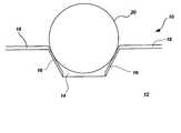
- FIG. 1is a cross-sectional schematic view of a bump plate 10 for testing the connect conductivity and quality of a solder ball on an unpackaged semiconductor die.
- Bump plate 10is fabricated in a semiconductor substrate 12 , such as, for example, silicon, gallium arsenide, or silicon on sapphire, to name a few.
- a plurality of receiving pits 14is formed in the surface of substrate 12 .
- Pit 14can be any desired polygonal or curved shape, but is preferred to be square with four sloped side walls 16 . Each wall 16 is at an angle of 54° from horizontal, conforming to the plane of the surface of the silicon substrate that can be used in fabricating bump plate 10 .
- the surface of the plateis coated with a thin layer insulator of about 200-300 Angstroms (such as Si Oxide) before the metal traces are formed.
- Electrical connection for testing for the presence of the solder balls on the dieis provided by metal traces 18 .
- Metal traces 18are made from a suitable metal and extend across the surface of substrate 12 and down walls 16 of pit 14 .
- a solder ball or bump 20can then be positioned within pit 14 and contact all four sloped walls 16 .
- Ball 20is placed within pit 14 when a die under test is mated with bump plate 10 . Since a metal trace 18 is placed on each wall 16 and extends across the surface of substrate 12 to an adjacent pit 14 , an applied electric current can flow through metal traces 18 provided the solder ball 20 contacts both sides of wall 16 and metal trace 18 thereon.
- FIG. 2depicts, in a cross-sectional perspective view, pit 14 prior to the addition of metal trace 18 of FIG. 1.
- Pit 14has a substantially flat bottom surface that is non-conductive as well as four adjacent side walls 16 , again having the slope angle that naturally slopes 54° in the surface plane of silicon substrate 12 as it is etched.
- the sloped wall 16allows for a spherical ball 20 to seat within pit 14 without damaging the bottom curvature of ball 20 while still contacting metal trace 18 that extends down the slope of wall 16 .
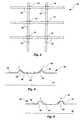
- Bump plate 10has a plurality of pits 14 and is shown in the schematic diagram of FIG. 3.
- Bump plate 10actually is an array of bump pits 14 that is electrically connected in rows and columns using metal traces 18 .
- Horizontal metal traces 18run across the surface of substrate 12 and down the sloped walls 16 of the bump pits 14 . It is important that metal traces 18 do not connect with one another within pits 14 .
- As an electric current is placed across each row and down each column in a sequential mannerit becomes readily apparent at each pit 14 location whether a ball exists or the connection is of such poor quality as to provide no conduction across the row or down the column. From this information, a grid map of the defects can be established that will allow repair of the missing or poor quality bumped locations at a subsequent repair stage.
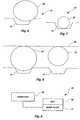
- FIG. 4illustrates a raised contact location 30 for contacting the bottom surface of a solder ball 20 .
- Each raised contact location 30comprises a set of side bumps 32 that form a valley 36 .
- a plurality of sharpened projections 34is formed within valley 36 and is designed to pierce the oxide layer formed over ball 20 and can be attached to adjacent metal traces 18 for providing good ohmic contact to adjacent metal traces 18 with ball 20 for testing purposes.
- Contact location 30can be in the shape of a polygon or circle and can be combined with pits 14 of FIG. 3.
- FIG. 5is an alternative embodiment where each pit 14 is replaced with a post trough 40 , which is formed by a plurality of posts 42 to form a polygon, such as a square. Posts 42 are formed such that a valley 44 is formed in post trough 40 . Metal traces are formed up and down the sides of post 42 , but not connecting one another in the same manner as traces 18 in FIG. 3. Thus, when a ball 20 is placed in a post trough 40 , a good ohmic connection forms between opposite traces 18 for conducting a test current. Further, post trough 40 can be in the shape of a polygon or circle and can be combined with pits 14 of FIG. 3 or contact locations 30 of FIG. 4.
- FIGS. 1 - 5Each of the embodiments of FIGS. 1 - 5 is capable of testing for various types of solder ball conditions. The most significant is when a missing ball occurs. This is simple to detect in that no current will flow either across the column or down the row when the test current is applied. Other examples are also possible and are illustrated in FIGS. 6, 7, and 8 .
- FIG. 6is an example of when a solder ball 20 is off center and only contacts one or two sides of pit 14 , thus preventing a good current signal from passing either across the column or down the row.
- FIG. 7is an example of a ball 20 too small to touch any sides in pit 14 . In this condition, no current can pass and it is viewed as being that no solder ball is present.
- FIG. 6is an example of when a solder ball 20 is off center and only contacts one or two sides of pit 14 , thus preventing a good current signal from passing either across the column or down the row.
- FIG. 7is an example of a ball 20 too small to touch any sides
- a first ball 20has a first diameter and a second ball 52 has a second diameter, which is much smaller than the first diameter of ball 20 .
- ball 20is an appropriate size and contacts well with the sides of pit 14 .
- ball 52is too small to even reach pit 14 , so the current signal test shows it as not being present at all.
- ball 52is actually the desired size of the balls while ball 20 is an aberration and is much larger than desired. This would be also be evident in that many balls would be seen as not being present as the diameter of ball 20 would prevent several adjacent balls from contacting in their respective pits.
- FIG. 9depicts a test apparatus 54 that uses a bump plate 10 .
- Apparatus 54comprises a signal processor, such as a computer system 56 , that attaches to a bump plate 10 . Electrical signals or current are passed to bump plate 10 along the rows and columns of the metal traces 18 to establish a test pattern.
- a device under test (DUT) 58is pressed upon bump plate 10 to match the solder ball pattern to the identical pattern fabricated on bump plate 10 . Once contact is made, the test is begun and the results are obtained more quickly compared to prior art test apparatus using optical or other mechanical means previously described.
- DUTdevice under test
- the bump die wafer inspection apparatus of the present inventionoffers the following advantages over the prior art. As the electronic world moves toward stencification miniaturization, better methods for testing these technologies are needed and this solution provides an advancement over those previously available and, using semiconductor fabrication techniques, a bump plate matching a desired solder ball pattern for a particular die can be generated.
- the silicon or other similar substratesserve as a rigid medium, and as a result of this rigidity, they have a fixed dimensional test capability for each bump/ball testing site. This limits its use with regard to the range of the dimensional tolerances that it can test. This is significant in that the bumps, or balls, or both, require tight dimensional tolerances to pass such testing.
- the silicon micro-machining and photolithography processesallow much more precise geometry control than the printed circuit board (PCB) or film technologies found in the prior art. Hence, a more definitive distinction and grading is made for each ball shape and position. Additionally, the present apparatus provides a unique methodology for electronically mapping the failing ball sites and then utilizing this map to direct a repair or rework system to correct each failing site. These operations of testing, mapping, and subsequent repair can be combined in a highly automated in-line process, thus reducing the necessary steps previously required in the prior art of removing the bad boards and sending them to the rework section of the fabrication operation.
- Another advantageis since the semiconductor substrate can be planarized to a uniform flatness compared to the PCB and other processing solutions, less damage is caused to the good solder balls attached to the DUT.
- the inventionprovides an improved method and system for testing a discrete, unpackaged semiconductor die having raised bond pads.
- specific materialshave been described, it is understood that other materials can be utilized.
- the method of the inventionhas been described with reference to certain specific embodiments as will be apparent to those skilled in the art, modifications can be made without departing from the scope of the invention as defined in the following claims.
Landscapes
- Physics & Mathematics (AREA)
- General Physics & Mathematics (AREA)
- Engineering & Computer Science (AREA)
- Computer Hardware Design (AREA)
- Microelectronics & Electronic Packaging (AREA)
- Testing Or Measuring Of Semiconductors Or The Like (AREA)
- Measuring Leads Or Probes (AREA)
- Testing Of Individual Semiconductor Devices (AREA)
Abstract
Description
- This application is a continuation of application Ser. No. 09/923,688, filed Aug. 6, 2001, pending, which is a continuation of application Ser. No. 09/521,592, filed Mar. 9, 2000, now U.S. Pat. No. 6,303,993 B1, issued Oct. 16, 2001, which is a divisional of application Ser. No. 08/994,004, filed Dec. 18, 1997, now U.S. Pat. No. 6,140,827, issued Oct. 31, 2000.[0001]
- The present invention relates generally to semiconductor manufacturing and, more particularly, to methods for testing semiconductor dice having raised or bumped bond pads. More particularly still, the present invention relates to fabricating and using a testing grid suitable for testing solder balls used for bumped bond pads on an unpackaged semiconductor die.[0002]
- Semiconductor dice are being fabricated with raised bond pads and are known as bumped semiconductor die. A bumped semiconductor die includes bond pads along with bumped solderable material such as a lead-tin alloy. These typically are manufactured from solder balls made of a lead-tin alloy. Bumped dies are often used for flip chip bonding where the die is mounted face down on the substrate, such as a printed circuit board, and then the die is attached to the substrate by welding or soldering. Typically, the bumps are formed as balls of materials that are circular in a cross-sectional plane parallel to the face of the die. The bumps typically have a diameter of from 50 micrometers (μm) to 100 μm. The sides of the bumps typically bow or curve outwardly from a flat top surface. The flat top surface forms the actual region of contact with a mating electrode on the printed circuit board or other substrate. In testing the attached solder bumps, a temporary electrical connection must be made between the contact locations or bond pads on the die and the external test circuitry associated with the testing apparatus. The bond pads provide a connection point for testing an integrated circuit on the die. Likewise, the integrity of each bump must be tested as well.[0003]
- In making this temporary electrical connection, it is desirable to effect a connection that causes as little damage as possible to the bumped die. If the temporary connection to the bumped bond pad damages the pad, the entire die may be ruined. This is difficult to accomplish because the connection must also produce a low resistance or ohmic contact with the bumped bond pad. A bond pad, with or without a bump, typically has a metal oxide layer formed over it that must be penetrated to make the ohmic contact.[0004]
- Some prior art contact structures, such as probe cards, scrape the bond pads and wipe away the oxide layer. This causes excess layer damage to the bond pads. Other interconnect structures, such as probe tips, may pierce the oxide layer and metal bond pad and leave a deep gouge. Still other interconnect structures, such as micro bumps, cannot even pierce the oxide layer, preventing the formation of an ohmic contact.[0005]
- In the past, following testing of a bump pad die, it has been necessary to reflow the bumps, which are typically damaged by the procedure. This is an additional process step that adds to the expense and complexity of the testing process. Furthermore, it requires heating the tested die that can adversely affect the integrated circuitry formed on the die.[0006]
- Other bond pad integrity testing systems have been developed in the prior art. Typically, these testing systems use optical imaging to determine the integrity of the weld connection on the bumped sites. One type of system is a profiling system that uses interferometry with robotic wafer handling to automate the testing step. The testing step develops a profile for measuring solder bump heights. Unfortunately, although the interferometry system does not damage the device in any way, the time required for analyzing each bump location can take from two to four minutes. This type of throughput is unacceptable when a high speed system is necessary.[0007]
- Accordingly, what is needed is a method and system for testing solder bumps in bond pad locations that does not damage the bond pads while improving throughput.[0008]
- According to the present invention, a method and apparatus for testing unpackaged semiconductor dice having raised contact locations are disclosed. The apparatus uses a temporary interconnect wafer that is adapted to establish an electrical connection with the raised ball contact locations on the die without damage to the ball contacts. The interconnect wafer is fabricated on a substrate, such as silicon, where contact members are formed in a pattern that matches the size and spacing of the contact locations on the die to be tested. The contact members on the interconnect wafer are formed as either pits, troughs, or spike contacts. The spike contacts penetrate through the oxide layer formed on the raised ball contact location. Conductive traces are provided in both rows and columns and are terminated on the inner edges of the walls of the pits formed in the substrate. This arrangement allows a system to measure the continuity across the bump pad or ball contact locations of the integrated circuit die in order to establish that each ball contact location is properly attached. This also allows the system to test for the presence and quality of the bump or ball contact locations on the particular die being tested.[0009]
- FIG. 1 is a schematic cross-sectional diagram of a pit formed in a substrate wherein a solder ball is received;[0010]
- FIG. 2 is a cross-sectional perspective schematic view of the pit according to FIG. 1;[0011]
- FIG. 3 is a top plan view of an array of pits according to that of FIG. 1 having a metal interconnect in a form of rows and columns;[0012]
- FIG. 4 is an alternative embodiment of the pit of FIG. 1 wherein raised supports are provided along with sharp blades for penetrating the ball;[0013]
- FIG. 5 is an alternative embodiment of the pit of FIG. 1 wherein raised portions are provided for penetrating the solder balls;[0014]
- FIG. 6 is an example of a solder ball being out of place and failing to make adequate connection between adjacent metal bonds;[0015]
- FIG. 7 is an example of when a ball that is too small has been identified;[0016]
- FIG. 8 is a schematic cross-sectional view of a device under test where mismatched balls are adjacent to one another; and,[0017]
- FIG. 9 is a block diagram of a test apparatus using the bump plate according to FIG. 3.[0018]
- FIG. 1 is a cross-sectional schematic view of a[0019]
bump plate 10 for testing the connect conductivity and quality of a solder ball on an unpackaged semiconductor die.Bump plate 10 is fabricated in asemiconductor substrate 12, such as, for example, silicon, gallium arsenide, or silicon on sapphire, to name a few. - A plurality of receiving[0020]
pits 14 is formed in the surface ofsubstrate 12.Pit 14 can be any desired polygonal or curved shape, but is preferred to be square with foursloped side walls 16. Eachwall 16 is at an angle of 54° from horizontal, conforming to the plane of the surface of the silicon substrate that can be used in fabricatingbump plate 10. After pits or suitable features are etched (formed), the surface of the plate is coated with a thin layer insulator of about 200-300 Angstroms (such as Si Oxide) before the metal traces are formed. Electrical connection for testing for the presence of the solder balls on the die is provided by metal traces18. Metal traces18 are made from a suitable metal and extend across the surface ofsubstrate 12 and downwalls 16 ofpit 14. A solder ball or bump20 can then be positioned withinpit 14 and contact all four slopedwalls 16.Ball 20 is placed withinpit 14 when a die under test is mated withbump plate 10. Since ametal trace 18 is placed on eachwall 16 and extends across the surface ofsubstrate 12 to anadjacent pit 14, an applied electric current can flow through metal traces18 provided thesolder ball 20 contacts both sides ofwall 16 andmetal trace 18 thereon. - A method that is adaptable for manufacturing[0021]
bump plate 10 is described in U.S. Pat. No. 5,592,736, “Fabricating An Interconnect For Testing Unpackaged Semiconductor Dice Having Raised Bond Pads,” commonly assigned to the same assignee as the present invention, and herein incorporated by reference for all purposes. - FIG. 2 depicts, in a cross-sectional perspective view,[0022]
pit 14 prior to the addition ofmetal trace 18 of FIG. 1.Pit 14 has a substantially flat bottom surface that is non-conductive as well as fouradjacent side walls 16, again having the slope angle that naturally slopes 54° in the surface plane ofsilicon substrate 12 as it is etched. The slopedwall 16 allows for aspherical ball 20 to seat withinpit 14 without damaging the bottom curvature ofball 20 while still contactingmetal trace 18 that extends down the slope ofwall 16. - [0023]
Bump plate 10 has a plurality ofpits 14 and is shown in the schematic diagram of FIG. 3.Bump plate 10 actually is an array of bump pits14 that is electrically connected in rows and columns using metal traces18. Horizontal metal traces18 run across the surface ofsubstrate 12 and down the slopedwalls 16 of the bump pits14. It is important that metal traces18 do not connect with one another within pits14. As an electric current is placed across each row and down each column in a sequential manner, it becomes readily apparent at eachpit 14 location whether a ball exists or the connection is of such poor quality as to provide no conduction across the row or down the column. From this information, a grid map of the defects can be established that will allow repair of the missing or poor quality bumped locations at a subsequent repair stage. - Alternative embodiments to[0024]
pits 14 within thesubstrate 12 are shown in FIGS. 4 and 5. FIG. 4 illustrates a raisedcontact location 30 for contacting the bottom surface of asolder ball 20. Each raisedcontact location 30 comprises a set of side bumps32 that form avalley 36. A plurality of sharpenedprojections 34 is formed withinvalley 36 and is designed to pierce the oxide layer formed overball 20 and can be attached to adjacent metal traces18 for providing good ohmic contact to adjacent metal traces18 withball 20 for testing purposes.Contact location 30 can be in the shape of a polygon or circle and can be combined withpits 14 of FIG. 3. - FIG. 5 is an alternative embodiment where each[0025]
pit 14 is replaced with apost trough 40, which is formed by a plurality ofposts 42 to form a polygon, such as a square.Posts 42 are formed such that avalley 44 is formed inpost trough 40. Metal traces are formed up and down the sides ofpost 42, but not connecting one another in the same manner as traces18 in FIG. 3. Thus, when aball 20 is placed in apost trough 40, a good ohmic connection forms betweenopposite traces 18 for conducting a test current. Further,post trough 40 can be in the shape of a polygon or circle and can be combined withpits 14 of FIG. 3 orcontact locations 30 of FIG. 4. - Each of the embodiments of FIGS.[0026]1-5 is capable of testing for various types of solder ball conditions. The most significant is when a missing ball occurs. This is simple to detect in that no current will flow either across the column or down the row when the test current is applied. Other examples are also possible and are illustrated in FIGS. 6, 7, and8. FIG. 6 is an example of when a
solder ball 20 is off center and only contacts one or two sides ofpit 14, thus preventing a good current signal from passing either across the column or down the row. FIG. 7 is an example of aball 20 too small to touch any sides inpit 14. In this condition, no current can pass and it is viewed as being that no solder ball is present. FIG. 8 depicts where adjacent balls of different sizes are attached to die50. Afirst ball 20 has a first diameter and asecond ball 52 has a second diameter, which is much smaller than the first diameter ofball 20. As is shown,ball 20 is an appropriate size and contacts well with the sides ofpit 14. By contrast,ball 52 is too small to even reachpit 14, so the current signal test shows it as not being present at all. Of course, the reverse can be true in thatball 52 is actually the desired size of the balls whileball 20 is an aberration and is much larger than desired. This would be also be evident in that many balls would be seen as not being present as the diameter ofball 20 would prevent several adjacent balls from contacting in their respective pits. - FIG. 9 depicts a[0027]
test apparatus 54 that uses abump plate 10.Apparatus 54 comprises a signal processor, such as acomputer system 56, that attaches to abump plate 10. Electrical signals or current are passed to bumpplate 10 along the rows and columns of the metal traces18 to establish a test pattern. A device under test (DUT)58 is pressed uponbump plate 10 to match the solder ball pattern to the identical pattern fabricated onbump plate 10. Once contact is made, the test is begun and the results are obtained more quickly compared to prior art test apparatus using optical or other mechanical means previously described. - The bump die wafer inspection apparatus of the present invention offers the following advantages over the prior art. As the electronic world moves toward stencification miniaturization, better methods for testing these technologies are needed and this solution provides an advancement over those previously available and, using semiconductor fabrication techniques, a bump plate matching a desired solder ball pattern for a particular die can be generated. The silicon or other similar substrates serve as a rigid medium, and as a result of this rigidity, they have a fixed dimensional test capability for each bump/ball testing site. This limits its use with regard to the range of the dimensional tolerances that it can test. This is significant in that the bumps, or balls, or both, require tight dimensional tolerances to pass such testing. The silicon micro-machining and photolithography processes allow much more precise geometry control than the printed circuit board (PCB) or film technologies found in the prior art. Hence, a more definitive distinction and grading is made for each ball shape and position. Additionally, the present apparatus provides a unique methodology for electronically mapping the failing ball sites and then utilizing this map to direct a repair or rework system to correct each failing site. These operations of testing, mapping, and subsequent repair can be combined in a highly automated in-line process, thus reducing the necessary steps previously required in the prior art of removing the bad boards and sending them to the rework section of the fabrication operation.[0028]
- Another advantage is since the semiconductor substrate can be planarized to a uniform flatness compared to the PCB and other processing solutions, less damage is caused to the good solder balls attached to the DUT.[0029]
- Thus the invention provides an improved method and system for testing a discrete, unpackaged semiconductor die having raised bond pads. Although specific materials have been described, it is understood that other materials can be utilized. Furthermore, although the method of the invention has been described with reference to certain specific embodiments as will be apparent to those skilled in the art, modifications can be made without departing from the scope of the invention as defined in the following claims.[0030]
Claims (6)
Priority Applications (4)
| Application Number | Priority Date | Filing Date | Title |
|---|---|---|---|
| US10/218,379US6927589B2 (en) | 1997-12-18 | 2002-08-13 | Apparatus for testing bumped die |
| US11/101,220US20050174134A1 (en) | 1997-12-18 | 2005-04-07 | Method and apparatus for testing bumped die |
| US11/601,546US20070063722A1 (en) | 1997-12-18 | 2006-11-17 | Method and apparatus for testing bumped die |
| US11/600,994US20070090855A1 (en) | 1997-12-18 | 2006-11-17 | Method and apparatus for testing bumped die |
Applications Claiming Priority (4)
| Application Number | Priority Date | Filing Date | Title |
|---|---|---|---|
| US08/994,004US6140827A (en) | 1997-12-18 | 1997-12-18 | Method and apparatus for testing bumped die |
| US09/521,592US6303993B1 (en) | 1997-12-18 | 2000-03-09 | Method and apparatus for testing bumped die |
| US09/923,688US6486552B2 (en) | 1997-12-18 | 2001-08-06 | Method and apparatus for testing bumped die |
| US10/218,379US6927589B2 (en) | 1997-12-18 | 2002-08-13 | Apparatus for testing bumped die |
Related Parent Applications (1)
| Application Number | Title | Priority Date | Filing Date |
|---|---|---|---|
| US09/923,688ContinuationUS6486552B2 (en) | 1997-12-18 | 2001-08-06 | Method and apparatus for testing bumped die |
Related Child Applications (1)
| Application Number | Title | Priority Date | Filing Date |
|---|---|---|---|
| US11/101,220ContinuationUS20050174134A1 (en) | 1997-12-18 | 2005-04-07 | Method and apparatus for testing bumped die |
Publications (2)
| Publication Number | Publication Date |
|---|---|
| US20020185301A1true US20020185301A1 (en) | 2002-12-12 |
| US6927589B2 US6927589B2 (en) | 2005-08-09 |
Family
ID=25540187
Family Applications (12)
| Application Number | Title | Priority Date | Filing Date |
|---|---|---|---|
| US08/994,004Expired - LifetimeUS6140827A (en) | 1997-12-18 | 1997-12-18 | Method and apparatus for testing bumped die |
| US09/521,932Expired - Fee RelatedUS6411118B1 (en) | 1997-12-18 | 2000-03-09 | Method and apparatus for testing bumped die |
| US09/521,592Expired - Fee RelatedUS6303993B1 (en) | 1997-12-18 | 2000-03-09 | Method and apparatus for testing bumped die |
| US09/521,332Expired - Fee RelatedUS6337574B1 (en) | 1997-12-18 | 2000-03-09 | Method and apparatus for testing bumped die |
| US09/923,460Expired - LifetimeUS6472894B1 (en) | 1997-12-18 | 2001-08-06 | Apparatus for testing bumped die |
| US09/923,688Expired - LifetimeUS6486552B2 (en) | 1997-12-18 | 2001-08-06 | Method and apparatus for testing bumped die |
| US10/173,957Expired - Fee RelatedUS7005870B2 (en) | 1997-12-18 | 2002-06-17 | Interconnect bump plate |
| US10/218,278Expired - LifetimeUS6630837B2 (en) | 1997-12-18 | 2002-08-13 | Apparatus for testing bumped die |
| US10/218,379Expired - Fee RelatedUS6927589B2 (en) | 1997-12-18 | 2002-08-13 | Apparatus for testing bumped die |
| US11/101,220AbandonedUS20050174134A1 (en) | 1997-12-18 | 2005-04-07 | Method and apparatus for testing bumped die |
| US11/600,994AbandonedUS20070090855A1 (en) | 1997-12-18 | 2006-11-17 | Method and apparatus for testing bumped die |
| US11/601,546AbandonedUS20070063722A1 (en) | 1997-12-18 | 2006-11-17 | Method and apparatus for testing bumped die |
Family Applications Before (8)
| Application Number | Title | Priority Date | Filing Date |
|---|---|---|---|
| US08/994,004Expired - LifetimeUS6140827A (en) | 1997-12-18 | 1997-12-18 | Method and apparatus for testing bumped die |
| US09/521,932Expired - Fee RelatedUS6411118B1 (en) | 1997-12-18 | 2000-03-09 | Method and apparatus for testing bumped die |
| US09/521,592Expired - Fee RelatedUS6303993B1 (en) | 1997-12-18 | 2000-03-09 | Method and apparatus for testing bumped die |
| US09/521,332Expired - Fee RelatedUS6337574B1 (en) | 1997-12-18 | 2000-03-09 | Method and apparatus for testing bumped die |
| US09/923,460Expired - LifetimeUS6472894B1 (en) | 1997-12-18 | 2001-08-06 | Apparatus for testing bumped die |
| US09/923,688Expired - LifetimeUS6486552B2 (en) | 1997-12-18 | 2001-08-06 | Method and apparatus for testing bumped die |
| US10/173,957Expired - Fee RelatedUS7005870B2 (en) | 1997-12-18 | 2002-06-17 | Interconnect bump plate |
| US10/218,278Expired - LifetimeUS6630837B2 (en) | 1997-12-18 | 2002-08-13 | Apparatus for testing bumped die |
Family Applications After (3)
| Application Number | Title | Priority Date | Filing Date |
|---|---|---|---|
| US11/101,220AbandonedUS20050174134A1 (en) | 1997-12-18 | 2005-04-07 | Method and apparatus for testing bumped die |
| US11/600,994AbandonedUS20070090855A1 (en) | 1997-12-18 | 2006-11-17 | Method and apparatus for testing bumped die |
| US11/601,546AbandonedUS20070063722A1 (en) | 1997-12-18 | 2006-11-17 | Method and apparatus for testing bumped die |
Country Status (1)
| Country | Link |
|---|---|
| US (12) | US6140827A (en) |
Cited By (1)
| Publication number | Priority date | Publication date | Assignee | Title |
|---|---|---|---|---|
| US20090152719A1 (en)* | 2007-12-18 | 2009-06-18 | Teck Kheng Lee | Methods of fluxless micro-piercing of solder balls, and resulting devices |
Families Citing this family (31)
| Publication number | Priority date | Publication date | Assignee | Title |
|---|---|---|---|---|
| US6140827A (en)* | 1997-12-18 | 2000-10-31 | Micron Technology, Inc. | Method and apparatus for testing bumped die |
| US6426642B1 (en)* | 1999-02-16 | 2002-07-30 | Micron Technology, Inc. | Insert for seating a microelectronic device having a protrusion and a plurality of raised-contacts |
| US6517669B2 (en)* | 1999-02-26 | 2003-02-11 | Micron Technology, Inc. | Apparatus and method of detecting endpoint of a dielectric etch |
| US6531664B1 (en)* | 1999-04-05 | 2003-03-11 | Delphi Technologies, Inc. | Surface mount devices with solder |
| US6263566B1 (en)* | 1999-05-03 | 2001-07-24 | Micron Technology, Inc. | Flexible semiconductor interconnect fabricated by backslide thinning |
| US6492738B2 (en)* | 1999-09-02 | 2002-12-10 | Micron Technology, Inc. | Apparatus and methods of testing and assembling bumped devices using an anisotropically conductive layer |
| US6320402B1 (en)* | 2000-02-03 | 2001-11-20 | Advanced Micro Devices Inc | Parallel inspection of semiconductor wafers by a plurality of different inspection stations to maximize throughput |
| GB2362132B8 (en)* | 2000-05-09 | 2011-07-20 | Matsushita Electric Industrial Co Ltd | Apparatus and method of screen printing |
| US6533590B1 (en)* | 2001-12-17 | 2003-03-18 | Hon Hai Precision Ind. Co., Ltd. | Ball grid array connector having improved contact configuration |
| US7064450B1 (en) | 2004-05-11 | 2006-06-20 | Xilinx, Inc. | Semiconductor die with high density offset-inline bond arrangement |
| US7235412B1 (en)* | 2004-05-11 | 2007-06-26 | Xilinx, Inc. | Semiconductor component having test pads and method and apparatus for testing same |
| US20060139045A1 (en)* | 2004-12-29 | 2006-06-29 | Wesley Gallagher | Device and method for testing unpackaged semiconductor die |
| US7501832B2 (en)* | 2005-02-28 | 2009-03-10 | Ridgetop Group, Inc. | Method and circuit for the detection of solder-joint failures in a digital electronic package |
| US7196294B2 (en)* | 2005-02-28 | 2007-03-27 | Ridgetop Group, Inc. | Method and resistive bridge circuit for the detection of solder-joint failures in a digital electronic package |
| US7662648B2 (en)* | 2005-08-31 | 2010-02-16 | Micron Technology, Inc. | Integrated circuit inspection system |
| US7494913B2 (en)* | 2006-08-31 | 2009-02-24 | Intel Corporation | Microball placement solutions |
| US20080144243A1 (en)* | 2006-12-19 | 2008-06-19 | Ridgetop Group, Inc. | Method and circuit for low-power detection of solder-joint network failures in digital electronic packages |
| TW200828477A (en)* | 2006-12-22 | 2008-07-01 | Advanpack Solutions Pte Ltd | Device and method for testing semiconductor element, and manufacturing method thereof |
| KR20080061021A (en)* | 2006-12-27 | 2008-07-02 | 동부일렉트로닉스 주식회사 | Semiconductor device and manufacturing method |
| US20080266820A1 (en)* | 2007-04-25 | 2008-10-30 | Vivek Amir Jairazbhoy | System for supporting and electrically grounding a cover of an electronic control module |
| US8756546B2 (en) | 2012-07-25 | 2014-06-17 | International Business Machines Corporation | Elastic modulus mapping of a chip carrier in a flip chip package |
| US8650512B1 (en) | 2012-11-15 | 2014-02-11 | International Business Machines Corporation | Elastic modulus mapping of an integrated circuit chip in a chip/device package |
| US9494618B2 (en)* | 2012-12-26 | 2016-11-15 | Translarity, Inc. | Designed asperity contactors, including nanospikes, for semiconductor test using a package, and associated systems and methods |
| US9583470B2 (en)* | 2013-12-19 | 2017-02-28 | Intel Corporation | Electronic device with solder pads including projections |
| KR102143490B1 (en)* | 2014-01-20 | 2020-08-12 | 에스케이하이닉스 주식회사 | Semiconductor apparatus having pad and bump |
| WO2017171857A1 (en)* | 2016-04-01 | 2017-10-05 | Intel Corporation | Systems and methods for replaceable ball grid array (bga) packages on board substrates |
| US10204841B1 (en)* | 2016-12-05 | 2019-02-12 | Xilinx, Inc. | Temporary connection traces for wafer sort testing |
| US20190013251A1 (en) | 2017-07-10 | 2019-01-10 | International Business Machines Corporation | Non-destructive testing of integrated circuit chips |
| CN109116058A (en)* | 2018-08-28 | 2019-01-01 | 慈溪市三佩机械有限公司 | A kind of engine throttle door cover plate circuit on-off test equipment |
| MX2022000327A (en)* | 2019-07-09 | 2022-05-24 | Elco Entpr Inc | DEVICE FOR FEEDING A WIRE ELECTRODE. |
| US11448603B1 (en)* | 2021-09-02 | 2022-09-20 | Axiomatique Technologies, Inc. | Methods and apparatuses for microscopy and spectroscopy in semiconductor systems |
Citations (51)
| Publication number | Priority date | Publication date | Assignee | Title |
|---|---|---|---|---|
| US229757A (en)* | 1880-07-06 | phoro-uthograpifeh | ||
| US231421A (en)* | 1880-08-24 | gillii ind | ||
| US2958064A (en)* | 1957-11-26 | 1960-10-25 | Amp Inc | Circuit board and socket construction |
| US3806800A (en)* | 1972-12-26 | 1974-04-23 | Ibm | Method and apparatus for determining the location of electrically conductive members on a structure |
| US4585991A (en)* | 1982-06-03 | 1986-04-29 | Texas Instruments Incorporated | Solid state multiprobe testing apparatus |
| US4792683A (en)* | 1987-01-16 | 1988-12-20 | Hughes Aircraft Company | Thermal technique for simultaneous testing of circuit board solder joints |
| US4838800A (en)* | 1988-05-23 | 1989-06-13 | Gte Products Corporation | High density interconnect system |
| US5058178A (en)* | 1989-12-21 | 1991-10-15 | At&T Bell Laboratories | Method and apparatus for inspection of specular, three-dimensional features |
| US5089772A (en)* | 1989-03-10 | 1992-02-18 | Matsushita Electric Industrial Co. Ltd. | Device for testing semiconductor integrated circuits and method of testing the same |
| US5108024A (en)* | 1991-06-03 | 1992-04-28 | Motorola, Inc. | Method of inspecting solder joints |
| US5177439A (en)* | 1991-08-30 | 1993-01-05 | U.S. Philips Corporation | Probe card for testing unencapsulated semiconductor devices |
| US5225037A (en)* | 1991-06-04 | 1993-07-06 | Texas Instruments Incorporated | Method for fabrication of probe card for testing of semiconductor devices |
| US5367253A (en)* | 1991-06-04 | 1994-11-22 | Micron Semiconductor, Inc. | Clamped carrier for testing of semiconductor dies |
| US5394490A (en)* | 1992-08-11 | 1995-02-28 | Hitachi, Ltd. | Semiconductor device having an optical waveguide interposed in the space between electrode members |
| US5479105A (en)* | 1993-06-25 | 1995-12-26 | Samsung Electronics Co., Ltd. | Known-good die testing apparatus |
| US5479694A (en)* | 1993-04-13 | 1996-01-02 | Micron Technology, Inc. | Method for mounting integrated circuits onto printed circuit boards and testing |
| US5495179A (en)* | 1991-06-04 | 1996-02-27 | Micron Technology, Inc. | Carrier having interchangeable substrate used for testing of semiconductor dies |
| US5510721A (en)* | 1994-12-19 | 1996-04-23 | Ford Motor Company | Method and adjustment for known good die testing using resilient conductive straps |
| US5523696A (en)* | 1993-06-14 | 1996-06-04 | International Business Machines Corp. | Method and apparatus for testing integrated circuit chips |
| US5530375A (en)* | 1992-12-24 | 1996-06-25 | International Business Machines Corporation | Method of testing circuits and/or burning-in chips |
| US5543724A (en)* | 1994-10-03 | 1996-08-06 | Motorola, Inc. | Method and apparatus for locating conductive features and testing semiconductor devices |
| US5550763A (en)* | 1994-05-02 | 1996-08-27 | Michael; David J. | Using cone shaped search models to locate ball bonds on wire bonded devices |
| US5585281A (en)* | 1995-02-03 | 1996-12-17 | Motorola, Inc. | Process and apparatus for forming and testing semiconductor package leads |
| US5592736A (en)* | 1993-09-03 | 1997-01-14 | Micron Technology, Inc. | Fabricating an interconnect for testing unpackaged semiconductor dice having raised bond pads |
| US5617209A (en)* | 1995-04-27 | 1997-04-01 | View Engineering, Inc. | Method and system for triangulation-based, 3-D imaging utilizing an angled scaning beam of radiant energy |
| US5646442A (en)* | 1994-09-16 | 1997-07-08 | Yamaichi Electronics Co., Ltd. | Contact structure for IC socket |
| US5703406A (en)* | 1995-09-22 | 1997-12-30 | Lg Semicon Co., Ltd. | Interconnection structure for attaching a semiconductor device to a substrate |
| US5758098A (en)* | 1994-05-12 | 1998-05-26 | Apple Computer, Inc. | Method and apparatus for providing a high throughput two-conductor serial interface with support for slave device detection |
| US5783865A (en)* | 1995-07-31 | 1998-07-21 | Fujitsu Limited | Wiring substrate and semiconductor device |
| US5787098A (en)* | 1996-07-29 | 1998-07-28 | International Business Machines Corporation | Complete chip I/O test through low contact testing using enhanced boundary scan |
| US5796591A (en)* | 1995-06-07 | 1998-08-18 | International Business Machines Corporation | Direct chip attach circuit card |
| US5834844A (en)* | 1995-03-24 | 1998-11-10 | Shinko Electric Industries Co., Ltd. | Semiconductor device having an element with circuit pattern thereon |
| US5877559A (en)* | 1995-06-12 | 1999-03-02 | Nitto Denko Corporation | Film carrier for fine-pitched and high density mounting and semiconductor device using same |
| US5883435A (en)* | 1996-07-25 | 1999-03-16 | International Business Machines Corporation | Personalization structure for semiconductor devices |
| US5920125A (en)* | 1992-11-12 | 1999-07-06 | International Business Machines Corporation | Interconnection of a carrier substrate and a semiconductor device |
| US5946553A (en)* | 1991-06-04 | 1999-08-31 | Micron Technology, Inc. | Process for manufacturing a semiconductor package with bi-substrate die |
| US5968945A (en)* | 1995-08-29 | 1999-10-19 | Celgene Corporation | Immunotherapeutic agents |
| US5994781A (en)* | 1997-05-30 | 1999-11-30 | Tessera, Inc. | Semiconductor chip package with dual layer terminal and lead structure |
| US6018249A (en)* | 1997-12-11 | 2000-01-25 | Micron Technolgoy, Inc. | Test system with mechanical alignment for semiconductor chip scale packages and dice |
| US6037667A (en)* | 1998-08-24 | 2000-03-14 | Micron Technology, Inc. | Socket assembly for use with solder ball |
| US6040702A (en)* | 1997-07-03 | 2000-03-21 | Micron Technology, Inc. | Carrier and system for testing bumped semiconductor components |
| US6046909A (en)* | 1998-11-16 | 2000-04-04 | Intel Corporation | Computer card with a printed circuit board with vias providing strength to the printed circuit board |
| US6075290A (en)* | 1998-02-26 | 2000-06-13 | National Semiconductor Corporation | Surface mount die: wafer level chip-scale package and process for making the same |
| US6091252A (en)* | 1997-03-25 | 2000-07-18 | Micron Technolopgy, Inc. | Method, apparatus and system for testing bumped semiconductor components |
| US6127736A (en)* | 1996-03-18 | 2000-10-03 | Micron Technology, Inc. | Microbump interconnect for semiconductor dice |
| US6140827A (en)* | 1997-12-18 | 2000-10-31 | Micron Technology, Inc. | Method and apparatus for testing bumped die |
| US6143989A (en)* | 1995-07-20 | 2000-11-07 | The Regents Of The University Of California | Active alignment/contact verification system |
| US6310484B1 (en)* | 1996-04-01 | 2001-10-30 | Micron Technology, Inc. | Semiconductor test interconnect with variable flexure contacts |
| US6362637B2 (en)* | 1996-12-31 | 2002-03-26 | Micron Technology, Inc. | Apparatus for testing semiconductor wafers including base with contact members and terminal contacts |
| US6380492B1 (en)* | 1999-11-12 | 2002-04-30 | Fujitsu Limited | Contact film used for devices having ball grid array structure and device mounting structure |
| US6411188B1 (en)* | 1998-03-27 | 2002-06-25 | Honeywell International Inc. | Amorphous metal transformer having a generally rectangular coil |
Family Cites Families (7)
| Publication number | Priority date | Publication date | Assignee | Title |
|---|---|---|---|---|
| US4423373A (en)* | 1981-03-16 | 1983-12-27 | Lecroy Research Systems Corporation | Test probe |
| US4858991A (en) | 1986-08-11 | 1989-08-22 | Eyvind Boyesen | Chair for infants |
| US4838991A (en)* | 1987-10-30 | 1989-06-13 | International Business Machines Corporation | Process for defining organic sidewall structures |
| US5446442A (en)* | 1992-03-31 | 1995-08-29 | Siemens Aktiengesellschaft | Circuit arrangement for triggering a vehicle passenger protection system |
| US5596736A (en)* | 1992-07-22 | 1997-01-21 | Fujitsu Limited | Data transfers to a backing store of a dynamically mapped data storage system in which data has nonsequential logical addresses |
| US5326428A (en)* | 1993-09-03 | 1994-07-05 | Micron Semiconductor, Inc. | Method for testing semiconductor circuitry for operability and method of forming apparatus for testing semiconductor circuitry for operability |
| US5965945A (en)* | 1998-11-12 | 1999-10-12 | Advanced Micro Devices, Inc. | Graded PB for C4 pump technology |
- 1997
- 1997-12-18USUS08/994,004patent/US6140827A/ennot_activeExpired - Lifetime
- 2000
- 2000-03-09USUS09/521,932patent/US6411118B1/ennot_activeExpired - Fee Related
- 2000-03-09USUS09/521,592patent/US6303993B1/ennot_activeExpired - Fee Related
- 2000-03-09USUS09/521,332patent/US6337574B1/ennot_activeExpired - Fee Related
- 2001
- 2001-08-06USUS09/923,460patent/US6472894B1/ennot_activeExpired - Lifetime
- 2001-08-06USUS09/923,688patent/US6486552B2/ennot_activeExpired - Lifetime
- 2002
- 2002-06-17USUS10/173,957patent/US7005870B2/ennot_activeExpired - Fee Related
- 2002-08-13USUS10/218,278patent/US6630837B2/ennot_activeExpired - Lifetime
- 2002-08-13USUS10/218,379patent/US6927589B2/ennot_activeExpired - Fee Related
- 2005
- 2005-04-07USUS11/101,220patent/US20050174134A1/ennot_activeAbandoned
- 2006
- 2006-11-17USUS11/600,994patent/US20070090855A1/ennot_activeAbandoned
- 2006-11-17USUS11/601,546patent/US20070063722A1/ennot_activeAbandoned
Patent Citations (53)
| Publication number | Priority date | Publication date | Assignee | Title |
|---|---|---|---|---|
| US229757A (en)* | 1880-07-06 | phoro-uthograpifeh | ||
| US231421A (en)* | 1880-08-24 | gillii ind | ||
| US2958064A (en)* | 1957-11-26 | 1960-10-25 | Amp Inc | Circuit board and socket construction |
| US3806800A (en)* | 1972-12-26 | 1974-04-23 | Ibm | Method and apparatus for determining the location of electrically conductive members on a structure |
| US4585991A (en)* | 1982-06-03 | 1986-04-29 | Texas Instruments Incorporated | Solid state multiprobe testing apparatus |
| US4792683A (en)* | 1987-01-16 | 1988-12-20 | Hughes Aircraft Company | Thermal technique for simultaneous testing of circuit board solder joints |
| US4838800A (en)* | 1988-05-23 | 1989-06-13 | Gte Products Corporation | High density interconnect system |
| US5089772A (en)* | 1989-03-10 | 1992-02-18 | Matsushita Electric Industrial Co. Ltd. | Device for testing semiconductor integrated circuits and method of testing the same |
| US5058178A (en)* | 1989-12-21 | 1991-10-15 | At&T Bell Laboratories | Method and apparatus for inspection of specular, three-dimensional features |
| US5108024A (en)* | 1991-06-03 | 1992-04-28 | Motorola, Inc. | Method of inspecting solder joints |
| US5367253A (en)* | 1991-06-04 | 1994-11-22 | Micron Semiconductor, Inc. | Clamped carrier for testing of semiconductor dies |
| US5495179A (en)* | 1991-06-04 | 1996-02-27 | Micron Technology, Inc. | Carrier having interchangeable substrate used for testing of semiconductor dies |
| US5225037A (en)* | 1991-06-04 | 1993-07-06 | Texas Instruments Incorporated | Method for fabrication of probe card for testing of semiconductor devices |
| US5946553A (en)* | 1991-06-04 | 1999-08-31 | Micron Technology, Inc. | Process for manufacturing a semiconductor package with bi-substrate die |
| US5177439A (en)* | 1991-08-30 | 1993-01-05 | U.S. Philips Corporation | Probe card for testing unencapsulated semiconductor devices |
| US5394490A (en)* | 1992-08-11 | 1995-02-28 | Hitachi, Ltd. | Semiconductor device having an optical waveguide interposed in the space between electrode members |
| US5920125A (en)* | 1992-11-12 | 1999-07-06 | International Business Machines Corporation | Interconnection of a carrier substrate and a semiconductor device |
| US5530375A (en)* | 1992-12-24 | 1996-06-25 | International Business Machines Corporation | Method of testing circuits and/or burning-in chips |
| US5479694A (en)* | 1993-04-13 | 1996-01-02 | Micron Technology, Inc. | Method for mounting integrated circuits onto printed circuit boards and testing |
| US5523696A (en)* | 1993-06-14 | 1996-06-04 | International Business Machines Corp. | Method and apparatus for testing integrated circuit chips |
| US5479105A (en)* | 1993-06-25 | 1995-12-26 | Samsung Electronics Co., Ltd. | Known-good die testing apparatus |
| US5592736A (en)* | 1993-09-03 | 1997-01-14 | Micron Technology, Inc. | Fabricating an interconnect for testing unpackaged semiconductor dice having raised bond pads |
| US5550763A (en)* | 1994-05-02 | 1996-08-27 | Michael; David J. | Using cone shaped search models to locate ball bonds on wire bonded devices |
| US5758098A (en)* | 1994-05-12 | 1998-05-26 | Apple Computer, Inc. | Method and apparatus for providing a high throughput two-conductor serial interface with support for slave device detection |
| US5646442A (en)* | 1994-09-16 | 1997-07-08 | Yamaichi Electronics Co., Ltd. | Contact structure for IC socket |
| US5543724A (en)* | 1994-10-03 | 1996-08-06 | Motorola, Inc. | Method and apparatus for locating conductive features and testing semiconductor devices |
| US5510721A (en)* | 1994-12-19 | 1996-04-23 | Ford Motor Company | Method and adjustment for known good die testing using resilient conductive straps |
| US5585281A (en)* | 1995-02-03 | 1996-12-17 | Motorola, Inc. | Process and apparatus for forming and testing semiconductor package leads |
| US5834844A (en)* | 1995-03-24 | 1998-11-10 | Shinko Electric Industries Co., Ltd. | Semiconductor device having an element with circuit pattern thereon |
| US5617209A (en)* | 1995-04-27 | 1997-04-01 | View Engineering, Inc. | Method and system for triangulation-based, 3-D imaging utilizing an angled scaning beam of radiant energy |
| US5796591A (en)* | 1995-06-07 | 1998-08-18 | International Business Machines Corporation | Direct chip attach circuit card |
| US5877559A (en)* | 1995-06-12 | 1999-03-02 | Nitto Denko Corporation | Film carrier for fine-pitched and high density mounting and semiconductor device using same |
| US6143989A (en)* | 1995-07-20 | 2000-11-07 | The Regents Of The University Of California | Active alignment/contact verification system |
| US5783865A (en)* | 1995-07-31 | 1998-07-21 | Fujitsu Limited | Wiring substrate and semiconductor device |
| US5968945A (en)* | 1995-08-29 | 1999-10-19 | Celgene Corporation | Immunotherapeutic agents |
| US5703406A (en)* | 1995-09-22 | 1997-12-30 | Lg Semicon Co., Ltd. | Interconnection structure for attaching a semiconductor device to a substrate |
| US6127736A (en)* | 1996-03-18 | 2000-10-03 | Micron Technology, Inc. | Microbump interconnect for semiconductor dice |
| US6310484B1 (en)* | 1996-04-01 | 2001-10-30 | Micron Technology, Inc. | Semiconductor test interconnect with variable flexure contacts |
| US5883435A (en)* | 1996-07-25 | 1999-03-16 | International Business Machines Corporation | Personalization structure for semiconductor devices |
| US5787098A (en)* | 1996-07-29 | 1998-07-28 | International Business Machines Corporation | Complete chip I/O test through low contact testing using enhanced boundary scan |
| US6362637B2 (en)* | 1996-12-31 | 2002-03-26 | Micron Technology, Inc. | Apparatus for testing semiconductor wafers including base with contact members and terminal contacts |
| US6091252A (en)* | 1997-03-25 | 2000-07-18 | Micron Technolopgy, Inc. | Method, apparatus and system for testing bumped semiconductor components |
| US5994781A (en)* | 1997-05-30 | 1999-11-30 | Tessera, Inc. | Semiconductor chip package with dual layer terminal and lead structure |
| US6040702A (en)* | 1997-07-03 | 2000-03-21 | Micron Technology, Inc. | Carrier and system for testing bumped semiconductor components |
| US6018249A (en)* | 1997-12-11 | 2000-01-25 | Micron Technolgoy, Inc. | Test system with mechanical alignment for semiconductor chip scale packages and dice |
| US6140827A (en)* | 1997-12-18 | 2000-10-31 | Micron Technology, Inc. | Method and apparatus for testing bumped die |
| US6303993B1 (en)* | 1997-12-18 | 2001-10-16 | Micron Technology, Inc. | Method and apparatus for testing bumped die |
| US6337574B1 (en)* | 1997-12-18 | 2002-01-08 | Micron Technology, Inc. | Method and apparatus for testing bumped die |
| US6075290A (en)* | 1998-02-26 | 2000-06-13 | National Semiconductor Corporation | Surface mount die: wafer level chip-scale package and process for making the same |
| US6411188B1 (en)* | 1998-03-27 | 2002-06-25 | Honeywell International Inc. | Amorphous metal transformer having a generally rectangular coil |
| US6037667A (en)* | 1998-08-24 | 2000-03-14 | Micron Technology, Inc. | Socket assembly for use with solder ball |
| US6046909A (en)* | 1998-11-16 | 2000-04-04 | Intel Corporation | Computer card with a printed circuit board with vias providing strength to the printed circuit board |
| US6380492B1 (en)* | 1999-11-12 | 2002-04-30 | Fujitsu Limited | Contact film used for devices having ball grid array structure and device mounting structure |
Cited By (7)
| Publication number | Priority date | Publication date | Assignee | Title |
|---|---|---|---|---|
| US20090152719A1 (en)* | 2007-12-18 | 2009-06-18 | Teck Kheng Lee | Methods of fluxless micro-piercing of solder balls, and resulting devices |
| US7749887B2 (en)* | 2007-12-18 | 2010-07-06 | Micron Technology, Inc. | Methods of fluxless micro-piercing of solder balls, and resulting devices |
| US20100264541A1 (en)* | 2007-12-18 | 2010-10-21 | Micron Technology, Inc. | Methods of fluxless micro-piercing of solder balls, and resulting devices |
| US8436478B2 (en) | 2007-12-18 | 2013-05-07 | Micron Technology, Inc. | Methods of fluxless micro-piercing of solder balls, and resulting devices |
| US8669173B2 (en) | 2007-12-18 | 2014-03-11 | Micron Technology | Methods of fluxless micro-piercing of solder balls, and resulting devices |
| US10163840B2 (en) | 2007-12-18 | 2018-12-25 | Micron Technology, Inc. | Methods of fluxless micro-piercing of solder balls, and resulting devices |
| US10515918B2 (en) | 2007-12-18 | 2019-12-24 | Micron Technology, Inc. | Methods of fluxless micro-piercing of solder balls, and resulting devices |
Also Published As
| Publication number | Publication date |
|---|---|
| US20050174134A1 (en) | 2005-08-11 |
| US6337574B1 (en) | 2002-01-08 |
| US6472894B1 (en) | 2002-10-29 |
| US7005870B2 (en) | 2006-02-28 |
| US6486552B2 (en) | 2002-11-26 |
| US20070090855A1 (en) | 2007-04-26 |
| US20020158655A1 (en) | 2002-10-31 |
| US6303993B1 (en) | 2001-10-16 |
| US6630837B2 (en) | 2003-10-07 |
| US6140827A (en) | 2000-10-31 |
| US20020196041A1 (en) | 2002-12-26 |
| US20010048153A1 (en) | 2001-12-06 |
| US6411118B1 (en) | 2002-06-25 |
| US6927589B2 (en) | 2005-08-09 |
| US20070063722A1 (en) | 2007-03-22 |
Similar Documents
| Publication | Publication Date | Title |
|---|---|---|
| US6927589B2 (en) | Apparatus for testing bumped die | |
| US6483328B1 (en) | Probe card for probing wafers with raised contact elements | |
| US6562641B1 (en) | Apparatus and methods of semiconductor packages having circuit-bearing interconnect components | |
| US20070132097A1 (en) | Projected contact structures for engaging bumped semiconductor devices | |
| US6100708A (en) | Probe card and wafer testing method using the same | |
| JPH10308423A (en) | Method of manufacturing semiconductor device and method of probing to semiconductor device | |
| US7271611B2 (en) | Method for testing semiconductor components using bonded electrical connections | |
| US6249114B1 (en) | Electronic component continuity inspection method and apparatus | |
| US7102372B2 (en) | Apparatus and method for testing conductive bumps | |
| KR100600230B1 (en) | Contactor for solder balls | |
| JP3214420B2 (en) | Film carrier type semiconductor device, inspection probe head, and alignment method | |
| EP0752594A2 (en) | Contact structure for electrically connecting a testing board and die | |
| JP2003031628A (en) | Method for manufacturing semiconductor device and method for probing to semiconductor device | |
| JP3178784B2 (en) | Inspection apparatus and inspection method for semiconductor package substrate | |
| JP2000012587A (en) | Electric characteristic inspection and coining method of solder bumps of circuit board for semiconductor chip mounting | |
| JP2000077599A (en) | Terminal inspection jig | |
| JP2002005957A (en) | Contact pin | |
| JP2002050876A (en) | Substrate and manufacturing method thereof | |
| US6429030B1 (en) | Method for testing a semiconductor die using wells | |
| JPH0212070A (en) | Manufacturing method for inspection equipment | |
| JPH1131763A (en) | Package structure for semiconductor part and method for testing soldered joint between part lead and circuit substrate | |
| JPH08203902A (en) | Method for manufacturing semiconductor device | |
| JPH09269351A (en) | Electrical connection inspection device for circuit board | |
| JPH0730300A (en) | Inspection equipment | |
| JP2005249670A (en) | Electrical characteristic evaluation measurement and bump leveling jig, method and apparatus for semiconductor device with bump, and semiconductor device with bump formed thereby |
Legal Events
| Date | Code | Title | Description |
|---|---|---|---|
| FEPP | Fee payment procedure | Free format text:PAYOR NUMBER ASSIGNED (ORIGINAL EVENT CODE: ASPN); ENTITY STATUS OF PATENT OWNER: LARGE ENTITY | |
| CC | Certificate of correction | ||
| FPAY | Fee payment | Year of fee payment:4 | |
| FPAY | Fee payment | Year of fee payment:8 | |
| AS | Assignment | Owner name:U.S. BANK NATIONAL ASSOCIATION, AS COLLATERAL AGENT, CALIFORNIA Free format text:SECURITY INTEREST;ASSIGNOR:MICRON TECHNOLOGY, INC.;REEL/FRAME:038669/0001 Effective date:20160426 Owner name:U.S. BANK NATIONAL ASSOCIATION, AS COLLATERAL AGEN Free format text:SECURITY INTEREST;ASSIGNOR:MICRON TECHNOLOGY, INC.;REEL/FRAME:038669/0001 Effective date:20160426 | |
| AS | Assignment | Owner name:MORGAN STANLEY SENIOR FUNDING, INC., AS COLLATERAL AGENT, MARYLAND Free format text:PATENT SECURITY AGREEMENT;ASSIGNOR:MICRON TECHNOLOGY, INC.;REEL/FRAME:038954/0001 Effective date:20160426 Owner name:MORGAN STANLEY SENIOR FUNDING, INC., AS COLLATERAL Free format text:PATENT SECURITY AGREEMENT;ASSIGNOR:MICRON TECHNOLOGY, INC.;REEL/FRAME:038954/0001 Effective date:20160426 | |
| REMI | Maintenance fee reminder mailed | ||
| AS | Assignment | Owner name:U.S. BANK NATIONAL ASSOCIATION, AS COLLATERAL AGENT, CALIFORNIA Free format text:CORRECTIVE ASSIGNMENT TO CORRECT THE REPLACE ERRONEOUSLY FILED PATENT #7358718 WITH THE CORRECT PATENT #7358178 PREVIOUSLY RECORDED ON REEL 038669 FRAME 0001. ASSIGNOR(S) HEREBY CONFIRMS THE SECURITY INTEREST;ASSIGNOR:MICRON TECHNOLOGY, INC.;REEL/FRAME:043079/0001 Effective date:20160426 Owner name:U.S. BANK NATIONAL ASSOCIATION, AS COLLATERAL AGEN Free format text:CORRECTIVE ASSIGNMENT TO CORRECT THE REPLACE ERRONEOUSLY FILED PATENT #7358718 WITH THE CORRECT PATENT #7358178 PREVIOUSLY RECORDED ON REEL 038669 FRAME 0001. ASSIGNOR(S) HEREBY CONFIRMS THE SECURITY INTEREST;ASSIGNOR:MICRON TECHNOLOGY, INC.;REEL/FRAME:043079/0001 Effective date:20160426 | |
| LAPS | Lapse for failure to pay maintenance fees | Free format text:PATENT EXPIRED FOR FAILURE TO PAY MAINTENANCE FEES (ORIGINAL EVENT CODE: EXP.) | |
| STCH | Information on status: patent discontinuation | Free format text:PATENT EXPIRED DUE TO NONPAYMENT OF MAINTENANCE FEES UNDER 37 CFR 1.362 | |
| FP | Lapsed due to failure to pay maintenance fee | Effective date:20170809 | |
| AS | Assignment | Owner name:MICRON TECHNOLOGY, INC., IDAHO Free format text:RELEASE BY SECURED PARTY;ASSIGNOR:U.S. BANK NATIONAL ASSOCIATION, AS COLLATERAL AGENT;REEL/FRAME:047243/0001 Effective date:20180629 | |
| AS | Assignment | Owner name:MICRON TECHNOLOGY, INC., IDAHO Free format text:RELEASE BY SECURED PARTY;ASSIGNOR:MORGAN STANLEY SENIOR FUNDING, INC., AS COLLATERAL AGENT;REEL/FRAME:050937/0001 Effective date:20190731 |