US20020177282A1 - Method of forming semiconductor device having a GAA type transistor - Google Patents
Method of forming semiconductor device having a GAA type transistorDownload PDFInfo
- Publication number
- US20020177282A1 US20020177282A1US10/022,934US2293401AUS2002177282A1US 20020177282 A1US20020177282 A1US 20020177282A1US 2293401 AUS2293401 AUS 2293401AUS 2002177282 A1US2002177282 A1US 2002177282A1
- Authority
- US
- United States
- Prior art keywords
- layer
- oxide layer
- layer pattern
- etch stopping
- pattern
- Prior art date
- Legal status (The legal status is an assumption and is not a legal conclusion. Google has not performed a legal analysis and makes no representation as to the accuracy of the status listed.)
- Granted
Links
Images


Classifications
- H—ELECTRICITY
- H01—ELECTRIC ELEMENTS
- H01L—SEMICONDUCTOR DEVICES NOT COVERED BY CLASS H10
- H01L21/00—Processes or apparatus adapted for the manufacture or treatment of semiconductor or solid state devices or of parts thereof
- H01L21/02—Manufacture or treatment of semiconductor devices or of parts thereof
- H01L21/04—Manufacture or treatment of semiconductor devices or of parts thereof the devices having potential barriers, e.g. a PN junction, depletion layer or carrier concentration layer
- H01L21/18—Manufacture or treatment of semiconductor devices or of parts thereof the devices having potential barriers, e.g. a PN junction, depletion layer or carrier concentration layer the devices having semiconductor bodies comprising elements of Group IV of the Periodic Table or AIIIBV compounds with or without impurities, e.g. doping materials
- H—ELECTRICITY
- H10—SEMICONDUCTOR DEVICES; ELECTRIC SOLID-STATE DEVICES NOT OTHERWISE PROVIDED FOR
- H10D—INORGANIC ELECTRIC SEMICONDUCTOR DEVICES
- H10D30/00—Field-effect transistors [FET]
- H10D30/01—Manufacture or treatment
- H10D30/021—Manufacture or treatment of FETs having insulated gates [IGFET]
- H10D30/031—Manufacture or treatment of FETs having insulated gates [IGFET] of thin-film transistors [TFT]
- H10D30/0321—Manufacture or treatment of FETs having insulated gates [IGFET] of thin-film transistors [TFT] comprising silicon, e.g. amorphous silicon or polysilicon
- H10D30/0323—Manufacture or treatment of FETs having insulated gates [IGFET] of thin-film transistors [TFT] comprising silicon, e.g. amorphous silicon or polysilicon comprising monocrystalline silicon
- H—ELECTRICITY
- H10—SEMICONDUCTOR DEVICES; ELECTRIC SOLID-STATE DEVICES NOT OTHERWISE PROVIDED FOR
- H10D—INORGANIC ELECTRIC SEMICONDUCTOR DEVICES
- H10D30/00—Field-effect transistors [FET]
- H10D30/60—Insulated-gate field-effect transistors [IGFET]
- H10D30/67—Thin-film transistors [TFT]
- H10D30/6729—Thin-film transistors [TFT] characterised by the electrodes
- H10D30/673—Thin-film transistors [TFT] characterised by the electrodes characterised by the shapes, relative sizes or dispositions of the gate electrodes
- H10D30/6735—Thin-film transistors [TFT] characterised by the electrodes characterised by the shapes, relative sizes or dispositions of the gate electrodes having gates fully surrounding the channels, e.g. gate-all-around
- H—ELECTRICITY
- H10—SEMICONDUCTOR DEVICES; ELECTRIC SOLID-STATE DEVICES NOT OTHERWISE PROVIDED FOR
- H10D—INORGANIC ELECTRIC SEMICONDUCTOR DEVICES
- H10D30/00—Field-effect transistors [FET]
- H10D30/60—Insulated-gate field-effect transistors [IGFET]
- H10D30/67—Thin-film transistors [TFT]
- H10D30/674—Thin-film transistors [TFT] characterised by the active materials
- H10D30/6741—Group IV materials, e.g. germanium or silicon carbide
- H10D30/6743—Silicon
- H10D30/6744—Monocrystalline silicon
Definitions
- the present inventionrelates to a method of fabricating a semiconductor device having a gate all around(GAA) structure transistor.
- a first methodemploys a silicon on insulator (SOI) type substrate, and another method involves forming a three-dimensional device, such as a vertical transistor.
- SOIsilicon on insulator
- the method of using the SOI type substrateprovides higher electric pressure resistivity than the method of using device region isolation of a junction, and can reduce the problem of current generation at the junction in an environment of high radiation.
- GAAgate all around
- an active region patternis conventionally formed of a SOI layer on an SOI type substrate.
- a gate electrode layeris formed to surround a channel portion of the active region pattern covered with a gate insulation layer at a gate electrode.
- U.S. Pat. Nos. 5,120,666 and 5,308,999disclose a method of fabricating the GAA structure transistor.
- the entire peripheral portion of the channel surrounded by the gate electrodecan be used as a channel, and thus, the effective channel width is increased.
- the channel widthdecreases according to the reduction of a device region, thereby decreasing current quantity in a conventional transistor.
- a channel depletion area formed at the channel peripheral portioncan be overlapped and thus, the total channel can form a perfect depletion area.
- a gate electrodeshould be formed upward and downward the active layer pattern.
- a complex fabrication procedureis required as compared to that of a conventional MOS transistor.
- the processbecomes complicated and the process expense increases.
- the objectcan be achieved by a method of fabricating a semiconductor device according to the present invention.
- the methodincludes the following steps. That is, a SOI substrate composed of a SOI layer, a buried oxide layer, and a bottom substrate layer is prepared.
- the SOI layeris patterned to form an active layer pattern.
- An etch stopping layer having an etch selectivity with respect to the buried oxide layer and the active layer patternis stacked on the active layer pattern.
- the etch stopping layeris patterned and removed at the gate region that crosses the active layer pattern at the channel region, to form an etch stopping layer pattern and to expose the buried oxide layer.
- the buried oxide layeris isotropically etched using the etch stopping layer pattern as an etch mask to form a cavity at the channel region beneath the active layer pattern.
- a conductive materialfills the cavity and the space between the etch stopping layer pattern at the gate region.
- the active layer pattern and the conductive material filling the cavityshould be electrically isolated.
- a gate insulation layermay be formed.
- the gate insulation layershould be formed at the insulation layer-removed part, that is, at the channel region surface of the active layer pattern, until the step of forming the cavity in order to compensate the insulation layer-removed part.
- FIGS. 1A through 9Cillustrate process steps according to the present invention.
- the ‘A’refers to a process plan
- the ‘B’refers to cross-sectional view cutting a plan of a figure ‘A’ in the direction of I-I
- the ‘C’refers to a cross-sectional view cutting a plan of a figure ‘A’ in the direction of 11 - 11 .
- a SOI substrateis composed of a SOI layer 30 ′, a buried oxide layer 20 , and a bottom semiconductor substrate 10 .
- the SOI layeris, for example, formed of a silicon-based single crystal layer.
- FIG. 1Ais a plan for illustrating the SOI substrate.
- FIGS. 1B and 1Care cross-sectional views cutting the SOI substrate of FIG. 1A in the I-I and II-II directions, respectively.
- one methodincludes the following steps. That is, a thermal oxide layer having a certain thickness is formed on the surface of a first bulk type substrate. A second bulk type substrate is prepared and the two substrates are welded together. The belly side of the first bulk type substrate is substantially removed by a chemical-mechanical polishing (CMP) technique. Further, it is possible to use a method such as oxygen ion-implantation for formation of the buried oxide layer.
- CMPchemical-mechanical polishing
- the thin film transistorhas both low conductivity in comparison with the SOI layer and low function as a channel, but the active layer pattern can be formed of a polysilicon layer instead of the SOI layer.
- the SOI layer 30 ′is patterned to form an active layer pattern 30 .
- the width and length of the active layer pattern 30can be adjusted as occasion demands. In the event that the width of the active layer pattern is formed relatively large, an under-cut is widened toward the source/drain regions during a subsequent step of isotropically etching the buried oxide layer. Thus, it is preferable that thickness of the active layer pattern is relatively small.
- the height of the active layer patternis determined when the SOI substrate is formed.
- the thickness of the buried oxide layeris above one micrometer, and the thickness of the silicon single crystal layer is about 1,000 ⁇ to 1,500 ⁇ .
- the surface of the active layer pattern 30is thermal-oxidized to form an insulation layer 40 to a thickness of about 100 ⁇ .
- the surface of the active layer pattern 30can be nitrified to form the insulation layer 40 under nitrogen ambient and a high dielectric layer can be deposited on the surface of the active layer by chemical vapor deposition (CVD).
- CVDchemical vapor deposition
- a channel ion-implantation processcan be performed before or after thermal oxidation.
- an etch stopping layer formed of silicon nitrideis stacked on the active layer pattern 30 covered with the insulation layer 40 .
- the etch stopping layercomprises a material having an etch selectivity with respect to the insulation layer 40 and the buried oxide layer 20 .
- the etch stopping layeris removed in the gate region through a patterning process, for example using photo-lithography, to form the etch stopping layer pattern 50 .
- both the insulation layer 40 and the buried oxide layer 20serve as an etch stopping layer, where the insulation layer 40 comprises a thermal oxide layer covering the active layer pattern 30 .
- a sidewall spacer 52remains at the sidewalls of the active layer pattern 30 covered by the insulation layer 40 .
- the gate regionis formed to the direction of crossing the active layer pattern, and overlapped with the channel region when the gate region is seen upward, where the channel region is a middle part of the active layer pattern 30 .
- the etch stopping layer pattern 50is removed in the gate region to expose the channel region of the active layer pattern 30 covered by the insulation layer 40 .
- a buried oxide layer 20 ′is isotropically etched using the channel region of the active layer pattern 30 exposed between the right etch stopping layer pattern 50 and the left etch stopping layer pattern 50 .
- the thermal oxide layer covering the channel region of the active layer patternis together removed and thus, only the portion of the insulation layer 42 protected by the etch stopping layer pattern 50 remains.
- isotropic etchinga wet-etching using a dilute fluoric acid solution and an isotropic dry-etching are employed. As the etching is performed, when the under-cut part formed to the channel region bottom is connected at the both sides of the active layer pattern 30 , a cavity 22 is formed in the channel region bottom.
- the thermal oxide layer between the sidewall spacer 52 and the active layer pattern 30is not well etched and remains because of a loading effect at the narrow gap between them.
- anisotropic dry-etchingis performed before entirely performing isotropic etching.
- wet-etchingcan be laterally performed toward the active layer pattern 30 .
- the width of the active layer pattern 30is formed narrowly in a conventional highly integrated semiconductor device. Thus, it is not very difficult to form a cavity 22 in process of lateral etching.
- a channel part insulation layer 45 functioning as a gate insulation layeris formed at the channel part surface of the active layer pattern 30 .
- the gate insulation layeris formed of a thermal oxide layer or a nitride layer through thermal oxidation or thermal nitrification, but the gate insulation layer can be formed of an aluminum oxide layer, a tantalum oxide layer, a titanium oxide layer, a zirconium oxide layer, a hafnium oxide layer or other high dielectrics such as BST or PZT by employing the CVD technique having a good step coverage or an atomic layer deposition (ALD) technique.
- ALDatomic layer deposition
- the channel part insulation layer 45Before forming the channel part insulation layer 45 , hydrogen heat-treatment can be performed in order to alleviate that the active layer pattern 30 of the channel region is angled.
- the thickness of the channel part insulation layer 45varies with the function of a transistor device, but should be 20 A to 50 A in a drive circuit device.
- a conductive material layer 60 composing the gate electrodeis stacked on the semiconductor substrate by the CVD technique.
- the gate region where the etch stopping layer is removedincluding the cavity 22 between the active layer pattern 30 of the channel region and the buried oxide layer 20 ′, is filled with a conductive material layer 60 .
- the conductive material layer 60is formed of a material having a superior gap-fill capability so as not to have any remaining gaps under the CVD technique.
- the conductive materialsilicon, silicon germanium, tungsten, tungsten nitride, a dual layer of a titanium nitride layer and tungsten, aluminum, molybdenum, and tantalum can be used.
- the conductive material layer 60 stacked on the etch stopping layer pattern 50 defining the gate regionis removed by an entire surface anisotropic etch or the CMP technique.
- the top surface of an etch stopping layer pattern 54is exposed to form the gate electrode 62 .
- the etch stopping layer pattern 54is entirely removed by phosphoric wet-etching.
- GAAgate all around
- a low concentration ion-implantationis performed in order to form an LDD type source/drain region of the active layer pattern 30 .
- an insulation spacer 70is formed at the sidewalls of the gate electrode 62 , and a high concentration ion-implantation is performed. Low and high concentration ion-implantations can be formed in the state that the thermal oxide layer of the source/drain regions is removed as occasion demands.
- an insulation layeris stacked and patterned to form a contact hole at the interlayer insulation layer.
- a contactcan be connected at the source/drain regions.
- the gate electrodecan be formed with the feature of a gate line, or external voltage can be applied at the gate electrode through an additional contact as in the source/drain regions.
- a GAA structure transistorcan be formed by employing a photo-lithography process only twice, and thus, the process can be simplified in comparison with the conventional approaches of fabricating a GAA structure transistor.
Landscapes
- Engineering & Computer Science (AREA)
- Physics & Mathematics (AREA)
- Condensed Matter Physics & Semiconductors (AREA)
- General Physics & Mathematics (AREA)
- Manufacturing & Machinery (AREA)
- Computer Hardware Design (AREA)
- Microelectronics & Electronic Packaging (AREA)
- Power Engineering (AREA)
- Thin Film Transistor (AREA)
- Electrodes Of Semiconductors (AREA)
Abstract
Description
- This application relies for priority upon Korean Patent Application No. 2001-28369, filed on May 23, 2001, the contents of which are herein incorporated by reference in their entirety.[0001]
- The present invention relates to a method of fabricating a semiconductor device having a gate all around(GAA) structure transistor.[0002]
- As semiconductor devices become more highly integrated, a number of methods have been developed in order to reduce the sizes of individual devices formed on the semiconductor substrate, and also maximize device performance. Two of the many methods are more common than the others. A first method employs a silicon on insulator (SOI) type substrate, and another method involves forming a three-dimensional device, such as a vertical transistor.[0003]
- In the first case of using the SOI type substrate, it is possible to perfectly isolate devices, thereby preventing neighboring devices from affecting each other in a highly integrated configuration. Further, the method of using the SOI type substrate provides higher electric pressure resistivity than the method of using device region isolation of a junction, and can reduce the problem of current generation at the junction in an environment of high radiation.[0004]
- As a representative approach for forming the three-dimensional device, there is the gate all around (GAA) structure. According to the GAA structure, an active region pattern is conventionally formed of a SOI layer on an SOI type substrate. A gate electrode layer is formed to surround a channel portion of the active region pattern covered with a gate insulation layer at a gate electrode. U.S. Pat. Nos. 5,120,666 and 5,308,999 disclose a method of fabricating the GAA structure transistor.[0005]
- In the channel, the entire peripheral portion of the channel surrounded by the gate electrode can be used as a channel, and thus, the effective channel width is increased. Thus, it is possible to solve the problem that the channel width decreases according to the reduction of a device region, thereby decreasing current quantity in a conventional transistor. Also, a channel depletion area formed at the channel peripheral portion can be overlapped and thus, the total channel can form a perfect depletion area.[0006]
- However, in order to form the GAA structure transistor, a gate electrode should be formed upward and downward the active layer pattern. In forming such a structure, a complex fabrication procedure is required as compared to that of a conventional MOS transistor. Thus, there is a problem that the process becomes complicated and the process expense increases.[0007]
- Therefore, it is an object of the present invention to provide a method of fabricating a semiconductor device having a GAA structure transistor, where the transistor device has an effect of widening a channel width.[0008]
- It is another object of the present invention to provide a method of fabricating a semiconductor device having a GAA structure transistor device, where the method can reduce the number of photo-lithography process to simplify the process in order to reduce process complexity when the GAA structure transistor is formed.[0009]
- The object can be achieved by a method of fabricating a semiconductor device according to the present invention. The method includes the following steps. That is, a SOI substrate composed of a SOI layer, a buried oxide layer, and a bottom substrate layer is prepared. The SOI layer is patterned to form an active layer pattern. An etch stopping layer having an etch selectivity with respect to the buried oxide layer and the active layer pattern is stacked on the active layer pattern. The etch stopping layer is patterned and removed at the gate region that crosses the active layer pattern at the channel region, to form an etch stopping layer pattern and to expose the buried oxide layer. The buried oxide layer is isotropically etched using the etch stopping layer pattern as an etch mask to form a cavity at the channel region beneath the active layer pattern. A conductive material fills the cavity and the space between the etch stopping layer pattern at the gate region.[0010]
- In the present invention, the active layer pattern and the conductive material filling the cavity should be electrically isolated. In order to isolate the active layer pattern from the conductive material, after the step of forming the cavity, a gate insulation layer may be formed. Also, in the event that the surface of the active layer pattern is thermal-oxidized or thermal-nitrified to form an insulation layer before stacking the etch stopping layer, the gate insulation layer should be formed at the insulation layer-removed part, that is, at the channel region surface of the active layer pattern, until the step of forming the cavity in order to compensate the insulation layer-removed part. Thus, thickness and composition of the insulation layer formed on the surface of the active layer pattern can be different from those of the insulation layer formed on the surfaces of the source/drain regions and the channel region, respectively.[0011]
- The foregoing and other objects, features and advantages of the invention will be apparent from the more particular description of preferred embodiments of the invention, as illustrated in the accompanying drawings in which like reference characters refer to the same parts throughout the different views. The drawings are not necessarily to scale, emphasis instead being placed upon illustrating the principles of the invention.[0012]
- FIGS. 1A through 9C illustrate process steps according to the present invention. In each figure, the ‘A’ refers to a process plan, the ‘B’ refers to cross-sectional view cutting a plan of a figure ‘A’ in the direction of I-I. The ‘C’ refers to a cross-sectional view cutting a plan of a figure ‘A’ in the direction of[0013]11-11.
- The present invention will now be described more fully hereinafter with reference to the accompanying drawings, in which preferred embodiments of the invention are shown. This invention may, however, be embodied in different forms and should not be construed as limited to the embodiments set forth herein. Rather, these embodiments are provided so that this disclosure will be thorough and complete, and will fully convey the scope of the invention to those skilled in the art.[0014]
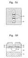
- Referring to FIGS. 1A, 1B and[0015]1C, a SOI substrate is composed of a
SOI layer 30′, a buriedoxide layer 20, and abottom semiconductor substrate 10. The SOI layer is, for example, formed of a silicon-based single crystal layer. FIG. 1A is a plan for illustrating the SOI substrate. FIGS. 1B and 1C are cross-sectional views cutting the SOI substrate of FIG. 1A in the I-I and II-II directions, respectively. - Several methods for fabricating the SOI substrate are possible. For example, one method includes the following steps. That is, a thermal oxide layer having a certain thickness is formed on the surface of a first bulk type substrate. A second bulk type substrate is prepared and the two substrates are welded together. The belly side of the first bulk type substrate is substantially removed by a chemical-mechanical polishing (CMP) technique. Further, it is possible to use a method such as oxygen ion-implantation for formation of the buried oxide layer.[0016]
- However, referring to the case of a thin film transistor, the thin film transistor has both low conductivity in comparison with the SOI layer and low function as a channel, but the active layer pattern can be formed of a polysilicon layer instead of the SOI layer.[0017]
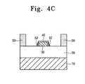
- Referring to FIGS. 2A, 2B, and[0018]2C, the
SOI layer 30′ is patterned to form anactive layer pattern 30. The width and length of theactive layer pattern 30 can be adjusted as occasion demands. In the event that the width of the active layer pattern is formed relatively large, an under-cut is widened toward the source/drain regions during a subsequent step of isotropically etching the buried oxide layer. Thus, it is preferable that thickness of the active layer pattern is relatively small. The height of the active layer pattern is determined when the SOI substrate is formed. Preferably, the thickness of the buried oxide layer is above one micrometer, and the thickness of the silicon single crystal layer is about 1,000 Å to 1,500 Å. - Referring to FIGS. 3A, 3B and[0019]3C, the surface of the
active layer pattern 30 is thermal-oxidized to form aninsulation layer 40 to a thickness of about 100 Å. The surface of theactive layer pattern 30 can be nitrified to form theinsulation layer 40 under nitrogen ambient and a high dielectric layer can be deposited on the surface of the active layer by chemical vapor deposition (CVD). A channel ion-implantation process can be performed before or after thermal oxidation. - Referring to FIGS. 4A, 4B and[0020]4C, an etch stopping layer formed of silicon nitride is stacked on the
active layer pattern 30 covered with theinsulation layer 40. Preferably, the etch stopping layer comprises a material having an etch selectivity with respect to theinsulation layer 40 and the buriedoxide layer 20. After stacking the etch stopping layer, the etch stopping layer is removed in the gate region through a patterning process, for example using photo-lithography, to form the etch stoppinglayer pattern 50. At this time, while anisotropic etching is performed, both theinsulation layer 40 and the buriedoxide layer 20 serve as an etch stopping layer, where theinsulation layer 40 comprises a thermal oxide layer covering theactive layer pattern 30. In the event that over-etching is not sufficiently performed in order to reduce the etch damage of theactive layer pattern 30 and to speed up process time, asidewall spacer 52 remains at the sidewalls of theactive layer pattern 30 covered by theinsulation layer 40. The gate region is formed to the direction of crossing the active layer pattern, and overlapped with the channel region when the gate region is seen upward, where the channel region is a middle part of theactive layer pattern 30. Thus, the etch stoppinglayer pattern 50 is removed in the gate region to expose the channel region of theactive layer pattern 30 covered by theinsulation layer 40. - Referring to FIGS. 5A, 5B, and[0021]5C, a buried
oxide layer 20′ is isotropically etched using the channel region of theactive layer pattern 30 exposed between the right etch stoppinglayer pattern 50 and the left etch stoppinglayer pattern 50. At this time, the thermal oxide layer covering the channel region of the active layer pattern is together removed and thus, only the portion of theinsulation layer 42 protected by the etch stoppinglayer pattern 50 remains. For isotropic etching, a wet-etching using a dilute fluoric acid solution and an isotropic dry-etching are employed. As the etching is performed, when the under-cut part formed to the channel region bottom is connected at the both sides of theactive layer pattern 30, acavity 22 is formed in the channel region bottom. The thermal oxide layer between thesidewall spacer 52 and theactive layer pattern 30 is not well etched and remains because of a loading effect at the narrow gap between them. - At this time, preferably, anisotropic dry-etching is performed before entirely performing isotropic etching. Next, wet-etching can be laterally performed toward the[0022]
active layer pattern 30. The width of theactive layer pattern 30 is formed narrowly in a conventional highly integrated semiconductor device. Thus, it is not very difficult to form acavity 22 in process of lateral etching. - Referring to FIGS. 6A, 6B and[0023]6C, after the thermal oxide layer is removed at the channel region of the active layer pattern, a channel
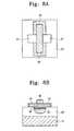
part insulation layer 45 functioning as a gate insulation layer is formed at the channel part surface of theactive layer pattern 30. Conventionally, the gate insulation layer is formed of a thermal oxide layer or a nitride layer through thermal oxidation or thermal nitrification, but the gate insulation layer can be formed of an aluminum oxide layer, a tantalum oxide layer, a titanium oxide layer, a zirconium oxide layer, a hafnium oxide layer or other high dielectrics such as BST or PZT by employing the CVD technique having a good step coverage or an atomic layer deposition (ALD) technique. Before forming the channelpart insulation layer 45, hydrogen heat-treatment can be performed in order to alleviate that theactive layer pattern 30 of the channel region is angled. The thickness of the channelpart insulation layer 45 varies with the function of a transistor device, but should be20A to50A in a drive circuit device. - A[0024]
conductive material layer 60 composing the gate electrode is stacked on the semiconductor substrate by the CVD technique. Thus, the gate region where the etch stopping layer is removed, including thecavity 22 between theactive layer pattern 30 of the channel region and the buriedoxide layer 20′, is filled with aconductive material layer 60. Preferably, theconductive material layer 60 is formed of a material having a superior gap-fill capability so as not to have any remaining gaps under the CVD technique. As the conductive material, silicon, silicon germanium, tungsten, tungsten nitride, a dual layer of a titanium nitride layer and tungsten, aluminum, molybdenum, and tantalum can be used. - Referring to FIGS. 7A, 7B and[0025]7C, the
conductive material layer 60 stacked on the etch stoppinglayer pattern 50 defining the gate region, is removed by an entire surface anisotropic etch or the CMP technique. Thus, the top surface of an etch stoppinglayer pattern 54 is exposed to form thegate electrode 62. - Referring to FIGS. 8A, 8B and[0026]8C, the etch stopping
layer pattern 54 is entirely removed by phosphoric wet-etching. Thus, it is possible to form a gate all around (GAA) structure transistor wherein the channel region of theactive layer pattern 30 is surrounded by thegate electrode 62, in the state that the channel portion of theinsulation layer 45 is interposed between the active5layer pattern 30 and thegate electrode 62. A low concentration ion-implantation is performed in order to form an LDD type source/drain region of theactive layer pattern 30. - Referring to FIGS. 9A, 9B and[0027]9C, an
insulation spacer 70 is formed at the sidewalls of thegate electrode 62, and a high concentration ion-implantation is performed. Low and high concentration ion-implantations can be formed in the state that the thermal oxide layer of the source/drain regions is removed as occasion demands. - Subsequently, an insulation layer is stacked and patterned to form a contact hole at the interlayer insulation layer. Thus, a contact can be connected at the source/drain regions. The gate electrode can be formed with the feature of a gate line, or external voltage can be applied at the gate electrode through an additional contact as in the source/drain regions.[0028]
- According to the present invention, a GAA structure transistor can be formed by employing a photo-lithography process only twice, and thus, the process can be simplified in comparison with the conventional approaches of fabricating a GAA structure transistor.[0029]
- While this invention has been particularly shown and described with references to preferred embodiments thereof, it will be understood by those skilled in the art that various changes in form and details may be made herein without departing from the spirit and scope of the invention as defined by the appended claims.[0030]
Claims (10)
Applications Claiming Priority (3)
| Application Number | Priority Date | Filing Date | Title |
|---|---|---|---|
| KR2001-28369 | 2001-05-23 | ||
| KR1020010028369AKR100363332B1 (en) | 2001-05-23 | 2001-05-23 | Method for forming semiconductor device having gate all-around type transistor |
| KR2001-0028369 | 2001-05-23 |
Publications (2)
| Publication Number | Publication Date |
|---|---|
| US20020177282A1true US20020177282A1 (en) | 2002-11-28 |
| US6537862B2 US6537862B2 (en) | 2003-03-25 |
Family
ID=19709830
Family Applications (1)
| Application Number | Title | Priority Date | Filing Date |
|---|---|---|---|
| US10/022,934Expired - LifetimeUS6537862B2 (en) | 2001-05-23 | 2001-12-18 | Method of forming semiconductor device having a GAA type transistor |
Country Status (4)
| Country | Link |
|---|---|
| US (1) | US6537862B2 (en) |
| JP (1) | JP4271901B2 (en) |
| KR (1) | KR100363332B1 (en) |
| TW (1) | TW506085B (en) |
Cited By (122)
| Publication number | Priority date | Publication date | Assignee | Title |
|---|---|---|---|---|
| US20020197863A1 (en)* | 2001-06-20 | 2002-12-26 | Mak Alfred W. | System and method to form a composite film stack utilizing sequential deposition techniques |
| US20030198754A1 (en)* | 2001-07-16 | 2003-10-23 | Ming Xi | Aluminum oxide chamber and process |
| US6638810B2 (en) | 2000-02-22 | 2003-10-28 | Applied Materials, Inc. | Tantalum nitride CVD deposition by tantalum oxide densification |
| US20030224578A1 (en)* | 2001-12-21 | 2003-12-04 | Hua Chung | Selective deposition of a barrier layer on a dielectric material |
| US6664156B1 (en)* | 2002-07-31 | 2003-12-16 | Chartered Semiconductor Manufacturing, Ltd | Method for forming L-shaped spacers with precise width control |
| US20030232511A1 (en)* | 2002-06-14 | 2003-12-18 | Applied Materials, Inc. | ALD metal oxide deposition process using direct oxidation |
| US20030232497A1 (en)* | 2002-04-16 | 2003-12-18 | Ming Xi | System and method for forming an integrated barrier layer |
| US20030232506A1 (en)* | 2002-06-14 | 2003-12-18 | Applied Materials, Inc. | System and method for forming a gate dielectric |
| US6718126B2 (en) | 2001-09-14 | 2004-04-06 | Applied Materials, Inc. | Apparatus and method for vaporizing solid precursor for CVD or atomic layer deposition |
| US6720027B2 (en) | 2002-04-08 | 2004-04-13 | Applied Materials, Inc. | Cyclical deposition of a variable content titanium silicon nitride layer |
| US6753248B1 (en) | 2003-01-27 | 2004-06-22 | Applied Materials, Inc. | Post metal barrier/adhesion film |
| US6772072B2 (en) | 2002-07-22 | 2004-08-03 | Applied Materials, Inc. | Method and apparatus for monitoring solid precursor delivery |
| US6773507B2 (en) | 2001-12-06 | 2004-08-10 | Applied Materials, Inc. | Apparatus and method for fast-cycle atomic layer deposition |
| US20040187304A1 (en)* | 2003-01-07 | 2004-09-30 | Applied Materials, Inc. | Enhancement of Cu line reliability using thin ALD TaN film to cap the Cu line |
| US6821563B2 (en) | 2002-10-02 | 2004-11-23 | Applied Materials, Inc. | Gas distribution system for cyclical layer deposition |
| US6831004B2 (en) | 2000-06-27 | 2004-12-14 | Applied Materials, Inc. | Formation of boride barrier layers using chemisorption techniques |
| US6838125B2 (en) | 2002-07-10 | 2005-01-04 | Applied Materials, Inc. | Method of film deposition using activated precursor gases |
| US6846516B2 (en) | 2002-04-08 | 2005-01-25 | Applied Materials, Inc. | Multiple precursor cyclical deposition system |
| US6905737B2 (en) | 2002-10-11 | 2005-06-14 | Applied Materials, Inc. | Method of delivering activated species for rapid cyclical deposition |
| US6911391B2 (en) | 2002-01-26 | 2005-06-28 | Applied Materials, Inc. | Integration of titanium and titanium nitride layers |
| US6915592B2 (en) | 2002-07-29 | 2005-07-12 | Applied Materials, Inc. | Method and apparatus for generating gas to a processing chamber |
| US6916398B2 (en) | 2001-10-26 | 2005-07-12 | Applied Materials, Inc. | Gas delivery apparatus and method for atomic layer deposition |
| US6936538B2 (en) | 2001-07-16 | 2005-08-30 | Applied Materials, Inc. | Method and apparatus for depositing tungsten after surface treatment to improve film characteristics |
| US6955211B2 (en) | 2002-07-17 | 2005-10-18 | Applied Materials, Inc. | Method and apparatus for gas temperature control in a semiconductor processing system |
| US6958296B2 (en) | 2001-05-07 | 2005-10-25 | Applied Materials, Inc. | CVD TiSiN barrier for copper integration |
| US6972267B2 (en) | 2002-03-04 | 2005-12-06 | Applied Materials, Inc. | Sequential deposition of tantalum nitride using a tantalum-containing precursor and a nitrogen-containing precursor |
| US20050285149A1 (en)* | 2004-06-28 | 2005-12-29 | Chang Peter L | Methods for forming semiconductor wires and resulting devices |
| US6998014B2 (en) | 2002-01-26 | 2006-02-14 | Applied Materials, Inc. | Apparatus and method for plasma assisted deposition |
| US20060084215A1 (en)* | 2003-12-05 | 2006-04-20 | Kabushiki Kaisha Toshiba | Semiconductor device and method for manufacturing the same |
| US7041335B2 (en) | 2002-06-04 | 2006-05-09 | Applied Materials, Inc. | Titanium tantalum nitride silicide layer |
| US7049226B2 (en) | 2001-09-26 | 2006-05-23 | Applied Materials, Inc. | Integration of ALD tantalum nitride for copper metallization |
| US7066194B2 (en) | 2002-07-19 | 2006-06-27 | Applied Materials, Inc. | Valve design and configuration for fast delivery system |
| US7081271B2 (en) | 2001-12-07 | 2006-07-25 | Applied Materials, Inc. | Cyclical deposition of refractory metal silicon nitride |
| US20060189157A1 (en)* | 2005-01-21 | 2006-08-24 | Stmicroelectronics S.A. | Method for forming an integrated circuit semiconductor substrate |
| US20060228868A1 (en)* | 2005-03-29 | 2006-10-12 | Micron Technology, Inc. | ALD of amorphous lanthanide doped TiOx films |
| US7135369B2 (en) | 2003-03-31 | 2006-11-14 | Micron Technology, Inc. | Atomic layer deposited ZrAlxOy dielectric layers including Zr4AlO9 |
| US7160577B2 (en)* | 2002-05-02 | 2007-01-09 | Micron Technology, Inc. | Methods for atomic-layer deposition of aluminum oxides in integrated circuits |
| US7175713B2 (en) | 2002-01-25 | 2007-02-13 | Applied Materials, Inc. | Apparatus for cyclical deposition of thin films |
| US7192824B2 (en)* | 2003-06-24 | 2007-03-20 | Micron Technology, Inc. | Lanthanide oxide / hafnium oxide dielectric layers |
| US7199023B2 (en) | 2002-08-28 | 2007-04-03 | Micron Technology, Inc. | Atomic layer deposited HfSiON dielectric films wherein each precursor is independendently pulsed |
| US7204886B2 (en) | 2002-11-14 | 2007-04-17 | Applied Materials, Inc. | Apparatus and method for hybrid chemical processing |
| US7208804B2 (en) | 2001-08-30 | 2007-04-24 | Micron Technology, Inc. | Crystalline or amorphous medium-K gate oxides, Y203 and Gd203 |
| US7211508B2 (en) | 2003-06-18 | 2007-05-01 | Applied Materials, Inc. | Atomic layer deposition of tantalum based barrier materials |
| US7220673B2 (en) | 2000-06-28 | 2007-05-22 | Applied Materials, Inc. | Method for depositing tungsten-containing layers by vapor deposition techniques |
| US7235854B2 (en) | 2002-08-15 | 2007-06-26 | Micron Technology, Inc. | Lanthanide doped TiOx dielectric films |
| US7235501B2 (en) | 2004-12-13 | 2007-06-26 | Micron Technology, Inc. | Lanthanum hafnium oxide dielectrics |
| US7241686B2 (en) | 2004-07-20 | 2007-07-10 | Applied Materials, Inc. | Atomic layer deposition of tantalum-containing materials using the tantalum precursor TAIMATA |
| US7244683B2 (en) | 2003-01-07 | 2007-07-17 | Applied Materials, Inc. | Integration of ALD/CVD barriers with porous low k materials |
| US7352048B2 (en) | 2001-09-26 | 2008-04-01 | Applied Materials, Inc. | Integration of barrier layer and seed layer |
| KR100822443B1 (en)* | 2004-06-28 | 2008-04-16 | 인텔 코포레이션 | Methods, semiconductor structures, devices, systems and memories for forming semiconductor lines |
| US7402534B2 (en) | 2005-08-26 | 2008-07-22 | Applied Materials, Inc. | Pretreatment processes within a batch ALD reactor |
| US7405454B2 (en) | 2003-03-04 | 2008-07-29 | Micron Technology, Inc. | Electronic apparatus with deposited dielectric layers |
| US7410668B2 (en) | 2001-03-01 | 2008-08-12 | Micron Technology, Inc. | Methods, systems, and apparatus for uniform chemical-vapor depositions |
| US7416979B2 (en) | 2001-07-25 | 2008-08-26 | Applied Materials, Inc. | Deposition methods for barrier and tungsten materials |
| US7429516B2 (en) | 2002-02-26 | 2008-09-30 | Applied Materials, Inc. | Tungsten nitride atomic layer deposition processes |
| US7429402B2 (en) | 2004-12-10 | 2008-09-30 | Applied Materials, Inc. | Ruthenium as an underlayer for tungsten film deposition |
| US7429361B2 (en) | 2002-07-17 | 2008-09-30 | Applied Materials, Inc. | Method and apparatus for providing precursor gas to a processing chamber |
| US7456476B2 (en)* | 2003-06-27 | 2008-11-25 | Intel Corporation | Nonplanar semiconductor device with partially or fully wrapped around gate electrode and methods of fabrication |
| US7465666B2 (en) | 2000-06-28 | 2008-12-16 | Applied Materials, Inc. | Method for forming tungsten materials during vapor deposition processes |
| US7470611B2 (en) | 1998-10-01 | 2008-12-30 | Applied Materials, Inc. | In situ deposition of a low K dielectric layer, barrier layer, etch stop, and anti-reflective coating for damascene application |
| US7494939B2 (en) | 2004-08-31 | 2009-02-24 | Micron Technology, Inc. | Methods for forming a lanthanum-metal oxide dielectric layer |
| US7521379B2 (en) | 2006-10-09 | 2009-04-21 | Applied Materials, Inc. | Deposition and densification process for titanium nitride barrier layers |
| US7547637B2 (en) | 2005-06-21 | 2009-06-16 | Intel Corporation | Methods for patterning a semiconductor film |
| US7547952B2 (en) | 2003-04-04 | 2009-06-16 | Applied Materials, Inc. | Method for hafnium nitride deposition |
| US7554161B2 (en) | 2002-06-05 | 2009-06-30 | Micron Technology, Inc. | HfAlO3 films for gate dielectrics |
| US7560793B2 (en) | 2002-05-02 | 2009-07-14 | Micron Technology, Inc. | Atomic layer deposition and conversion |
| US7582549B2 (en) | 2006-08-25 | 2009-09-01 | Micron Technology, Inc. | Atomic layer deposited barium strontium titanium oxide films |
| US7585762B2 (en) | 2007-09-25 | 2009-09-08 | Applied Materials, Inc. | Vapor deposition processes for tantalum carbide nitride materials |
| US7588988B2 (en) | 2004-08-31 | 2009-09-15 | Micron Technology, Inc. | Method of forming apparatus having oxide films formed using atomic layer deposition |
| US7611990B2 (en) | 2001-07-25 | 2009-11-03 | Applied Materials, Inc. | Deposition methods for barrier and tungsten materials |
| DE102005006153B4 (en)* | 2004-02-10 | 2010-02-04 | Samsung Electronics Co., Ltd., Suwon | Method for producing a field effect transistor (FET) |
| US7659158B2 (en) | 2008-03-31 | 2010-02-09 | Applied Materials, Inc. | Atomic layer deposition processes for non-volatile memory devices |
| US7662729B2 (en) | 2005-04-28 | 2010-02-16 | Micron Technology, Inc. | Atomic layer deposition of a ruthenium layer to a lanthanide oxide dielectric layer |
| US7678298B2 (en) | 2007-09-25 | 2010-03-16 | Applied Materials, Inc. | Tantalum carbide nitride materials by vapor deposition processes |
| US7682946B2 (en) | 2005-11-04 | 2010-03-23 | Applied Materials, Inc. | Apparatus and process for plasma-enhanced atomic layer deposition |
| US7682984B2 (en) | 2003-09-26 | 2010-03-23 | Applied Materials, Inc. | Interferometer endpoint monitoring device |
| US7709402B2 (en) | 2006-02-16 | 2010-05-04 | Micron Technology, Inc. | Conductive layers for hafnium silicon oxynitride films |
| US7719065B2 (en) | 2004-08-26 | 2010-05-18 | Micron Technology, Inc. | Ruthenium layer for a dielectric layer containing a lanthanide oxide |
| US7736956B2 (en) | 2005-08-17 | 2010-06-15 | Intel Corporation | Lateral undercut of metal gate in SOI device |
| US7745333B2 (en) | 2000-06-28 | 2010-06-29 | Applied Materials, Inc. | Methods for depositing tungsten layers employing atomic layer deposition techniques |
| US7780785B2 (en) | 2001-10-26 | 2010-08-24 | Applied Materials, Inc. | Gas delivery apparatus for atomic layer deposition |
| US7781771B2 (en) | 2004-03-31 | 2010-08-24 | Intel Corporation | Bulk non-planar transistor having strained enhanced mobility and methods of fabrication |
| US7794544B2 (en) | 2004-05-12 | 2010-09-14 | Applied Materials, Inc. | Control of gas flow and delivery to suppress the formation of particles in an MOCVD/ALD system |
| US7798096B2 (en) | 2006-05-05 | 2010-09-21 | Applied Materials, Inc. | Plasma, UV and ion/neutral assisted ALD or CVD in a batch tool |
| US7824743B2 (en) | 2007-09-28 | 2010-11-02 | Applied Materials, Inc. | Deposition processes for titanium nitride barrier and aluminum |
| US7879675B2 (en) | 2005-03-14 | 2011-02-01 | Intel Corporation | Field effect transistor with metal source/drain regions |
| US7898041B2 (en) | 2005-06-30 | 2011-03-01 | Intel Corporation | Block contact architectures for nanoscale channel transistors |
| US7902014B2 (en) | 2005-09-28 | 2011-03-08 | Intel Corporation | CMOS devices with a single work function gate electrode and method of fabrication |
| US7960794B2 (en) | 2004-08-10 | 2011-06-14 | Intel Corporation | Non-planar pMOS structure with a strained channel region and an integrated strained CMOS flow |
| US7989280B2 (en) | 2005-11-30 | 2011-08-02 | Intel Corporation | Dielectric interface for group III-V semiconductor device |
| US8067818B2 (en) | 2004-10-25 | 2011-11-29 | Intel Corporation | Nonplanar device with thinned lower body portion and method of fabrication |
| US8071167B2 (en) | 2002-06-14 | 2011-12-06 | Applied Materials, Inc. | Surface pre-treatment for enhancement of nucleation of high dielectric constant materials |
| US8084818B2 (en) | 2004-06-30 | 2011-12-27 | Intel Corporation | High mobility tri-gate devices and methods of fabrication |
| US8093638B2 (en) | 2002-06-05 | 2012-01-10 | Micron Technology, Inc. | Systems with a gate dielectric having multiple lanthanide oxide layers |
| US8092695B2 (en) | 2006-10-30 | 2012-01-10 | Applied Materials, Inc. | Endpoint detection for photomask etching |
| US8110489B2 (en) | 2001-07-25 | 2012-02-07 | Applied Materials, Inc. | Process for forming cobalt-containing materials |
| US8110469B2 (en) | 2005-08-30 | 2012-02-07 | Micron Technology, Inc. | Graded dielectric layers |
| US8119210B2 (en) | 2004-05-21 | 2012-02-21 | Applied Materials, Inc. | Formation of a silicon oxynitride layer on a high-k dielectric material |
| US8146896B2 (en) | 2008-10-31 | 2012-04-03 | Applied Materials, Inc. | Chemical precursor ampoule for vapor deposition processes |
| CN102437048A (en)* | 2011-08-04 | 2012-05-02 | 上海华力微电子有限公司 | Method for improving through hole etching of overlapping area of double through hole etching stop layers and device thereof |
| US8183646B2 (en) | 2005-02-23 | 2012-05-22 | Intel Corporation | Field effect transistor with narrow bandgap source and drain regions and method of fabrication |
| US8187970B2 (en) | 2001-07-25 | 2012-05-29 | Applied Materials, Inc. | Process for forming cobalt and cobalt silicide materials in tungsten contact applications |
| US8193567B2 (en) | 2005-09-28 | 2012-06-05 | Intel Corporation | Process for integrating planar and non-planar CMOS transistors on a bulk substrate and article made thereby |
| US8268709B2 (en) | 2004-09-29 | 2012-09-18 | Intel Corporation | Independently accessed double-gate and tri-gate transistors in same process flow |
| US8323754B2 (en) | 2004-05-21 | 2012-12-04 | Applied Materials, Inc. | Stabilization of high-k dielectric materials |
| US8362566B2 (en) | 2008-06-23 | 2013-01-29 | Intel Corporation | Stress in trigate devices using complimentary gate fill materials |
| US8405164B2 (en) | 2003-06-27 | 2013-03-26 | Intel Corporation | Tri-gate transistor device with stress incorporation layer and method of fabrication |
| US8491967B2 (en) | 2008-09-08 | 2013-07-23 | Applied Materials, Inc. | In-situ chamber treatment and deposition process |
| US8501563B2 (en) | 2005-07-20 | 2013-08-06 | Micron Technology, Inc. | Devices with nanocrystals and methods of formation |
| US8617945B2 (en) | 2006-08-02 | 2013-12-31 | Intel Corporation | Stacking fault and twin blocking barrier for integrating III-V on Si |
| US8778204B2 (en) | 2010-10-29 | 2014-07-15 | Applied Materials, Inc. | Methods for reducing photoresist interference when monitoring a target layer in a plasma process |
| US8778574B2 (en) | 2012-11-30 | 2014-07-15 | Applied Materials, Inc. | Method for etching EUV material layers utilized to form a photomask |
| US8791506B2 (en) | 2006-08-28 | 2014-07-29 | Micron Technology, Inc. | Semiconductor devices, assemblies and constructions |
| US8808559B2 (en) | 2011-11-22 | 2014-08-19 | Applied Materials, Inc. | Etch rate detection for reflective multi-material layers etching |
| US8900469B2 (en) | 2011-12-19 | 2014-12-02 | Applied Materials, Inc. | Etch rate detection for anti-reflective coating layer and absorber layer etching |
| US8961804B2 (en) | 2011-10-25 | 2015-02-24 | Applied Materials, Inc. | Etch rate detection for photomask etching |
| US9051641B2 (en) | 2001-07-25 | 2015-06-09 | Applied Materials, Inc. | Cobalt deposition on barrier surfaces |
| US9263455B2 (en) | 2013-07-23 | 2016-02-16 | Micron Technology, Inc. | Methods of forming an array of conductive lines and methods of forming an array of recessed access gate lines |
| US9337307B2 (en) | 2005-06-15 | 2016-05-10 | Intel Corporation | Method for fabricating transistor with thinned channel |
| US9418890B2 (en) | 2008-09-08 | 2016-08-16 | Applied Materials, Inc. | Method for tuning a deposition rate during an atomic layer deposition process |
| US9805939B2 (en) | 2012-10-12 | 2017-10-31 | Applied Materials, Inc. | Dual endpoint detection for advanced phase shift and binary photomasks |
| US10217842B2 (en)* | 2016-12-15 | 2019-02-26 | Commissariat A L'energie Atomique Et Aux Energies Alternatives | Method for making a semiconductor device with self-aligned inner spacers |
Families Citing this family (13)
| Publication number | Priority date | Publication date | Assignee | Title |
|---|---|---|---|---|
| JP2005005509A (en)* | 2003-06-12 | 2005-01-06 | Canon Inc | Thin film transistor and manufacturing method thereof |
| US6955969B2 (en)* | 2003-09-03 | 2005-10-18 | Advanced Micro Devices, Inc. | Method of growing as a channel region to reduce source/drain junction capacitance |
| US7268058B2 (en)* | 2004-01-16 | 2007-09-11 | Intel Corporation | Tri-gate transistors and methods to fabricate same |
| US8450806B2 (en)* | 2004-03-31 | 2013-05-28 | International Business Machines Corporation | Method for fabricating strained silicon-on-insulator structures and strained silicon-on insulator structures formed thereby |
| US7989855B2 (en) | 2004-06-10 | 2011-08-02 | Nec Corporation | Semiconductor device including a deflected part |
| US7332439B2 (en)* | 2004-09-29 | 2008-02-19 | Intel Corporation | Metal gate transistors with epitaxial source and drain regions |
| US7361958B2 (en)* | 2004-09-30 | 2008-04-22 | Intel Corporation | Nonplanar transistors with metal gate electrodes |
| US20070090408A1 (en)* | 2005-09-29 | 2007-04-26 | Amlan Majumdar | Narrow-body multiple-gate FET with dominant body transistor for high performance |
| JP4525928B2 (en)* | 2005-12-27 | 2010-08-18 | セイコーエプソン株式会社 | Manufacturing method of semiconductor device |
| US7498211B2 (en)* | 2005-12-28 | 2009-03-03 | Intel Corporation | Independently controlled, double gate nanowire memory cell with self-aligned contacts |
| KR100745909B1 (en)* | 2006-07-24 | 2007-08-02 | 주식회사 하이닉스반도체 | Manufacturing Method of Semiconductor Device |
| US8815691B2 (en) | 2012-12-21 | 2014-08-26 | Taiwan Semiconductor Manufacturing Company, Ltd. | Method of fabricating a gate all around device |
| JP6281420B2 (en)* | 2014-06-10 | 2018-02-21 | 富士通セミコンダクター株式会社 | Manufacturing method of semiconductor device |
Family Cites Families (6)
| Publication number | Priority date | Publication date | Assignee | Title |
|---|---|---|---|---|
| JPH02302044A (en) | 1989-05-16 | 1990-12-14 | Fujitsu Ltd | Manufacturing method of semiconductor device |
| JPH05243572A (en)* | 1992-02-27 | 1993-09-21 | Fujitsu Ltd | Semiconductor device |
| US5736435A (en)* | 1995-07-03 | 1998-04-07 | Motorola, Inc. | Process for fabricating a fully self-aligned soi mosfet |
| US6004837A (en)* | 1998-02-18 | 1999-12-21 | International Business Machines Corporation | Dual-gate SOI transistor |
| JP3699823B2 (en)* | 1998-05-19 | 2005-09-28 | 株式会社東芝 | Semiconductor device |
| US6040243A (en)* | 1999-09-20 | 2000-03-21 | Chartered Semiconductor Manufacturing Ltd. | Method to form copper damascene interconnects using a reverse barrier metal scheme to eliminate copper diffusion |
- 2001
- 2001-05-23KRKR1020010028369Apatent/KR100363332B1/ennot_activeExpired - Fee Related
- 2001-09-20TWTW090123175Apatent/TW506085B/enactive
- 2001-12-18USUS10/022,934patent/US6537862B2/ennot_activeExpired - Lifetime
- 2002
- 2002-05-21JPJP2002146860Apatent/JP4271901B2/ennot_activeExpired - Fee Related
Cited By (234)
| Publication number | Priority date | Publication date | Assignee | Title |
|---|---|---|---|---|
| US7670945B2 (en) | 1998-10-01 | 2010-03-02 | Applied Materials, Inc. | In situ deposition of a low κ dielectric layer, barrier layer, etch stop, and anti-reflective coating for damascene application |
| US7470611B2 (en) | 1998-10-01 | 2008-12-30 | Applied Materials, Inc. | In situ deposition of a low K dielectric layer, barrier layer, etch stop, and anti-reflective coating for damascene application |
| US6638810B2 (en) | 2000-02-22 | 2003-10-28 | Applied Materials, Inc. | Tantalum nitride CVD deposition by tantalum oxide densification |
| US7501343B2 (en) | 2000-06-27 | 2009-03-10 | Applied Materials, Inc. | Formation of boride barrier layers using chemisorption techniques |
| US6831004B2 (en) | 2000-06-27 | 2004-12-14 | Applied Materials, Inc. | Formation of boride barrier layers using chemisorption techniques |
| US7501344B2 (en) | 2000-06-27 | 2009-03-10 | Applied Materials, Inc. | Formation of boride barrier layers using chemisorption techniques |
| US7208413B2 (en) | 2000-06-27 | 2007-04-24 | Applied Materials, Inc. | Formation of boride barrier layers using chemisorption techniques |
| US7220673B2 (en) | 2000-06-28 | 2007-05-22 | Applied Materials, Inc. | Method for depositing tungsten-containing layers by vapor deposition techniques |
| US7465665B2 (en) | 2000-06-28 | 2008-12-16 | Applied Materials, Inc. | Method for depositing tungsten-containing layers by vapor deposition techniques |
| US7745333B2 (en) | 2000-06-28 | 2010-06-29 | Applied Materials, Inc. | Methods for depositing tungsten layers employing atomic layer deposition techniques |
| US7465666B2 (en) | 2000-06-28 | 2008-12-16 | Applied Materials, Inc. | Method for forming tungsten materials during vapor deposition processes |
| US7709385B2 (en) | 2000-06-28 | 2010-05-04 | Applied Materials, Inc. | Method for depositing tungsten-containing layers by vapor deposition techniques |
| US20070218688A1 (en)* | 2000-06-28 | 2007-09-20 | Ming Xi | Method for depositing tungsten-containing layers by vapor deposition techniques |
| US7846840B2 (en) | 2000-06-28 | 2010-12-07 | Applied Materials, Inc. | Method for forming tungsten materials during vapor deposition processes |
| US7674715B2 (en) | 2000-06-28 | 2010-03-09 | Applied Materials, Inc. | Method for forming tungsten materials during vapor deposition processes |
| US7410668B2 (en) | 2001-03-01 | 2008-08-12 | Micron Technology, Inc. | Methods, systems, and apparatus for uniform chemical-vapor depositions |
| US6958296B2 (en) | 2001-05-07 | 2005-10-25 | Applied Materials, Inc. | CVD TiSiN barrier for copper integration |
| US20020197863A1 (en)* | 2001-06-20 | 2002-12-26 | Mak Alfred W. | System and method to form a composite film stack utilizing sequential deposition techniques |
| US6849545B2 (en) | 2001-06-20 | 2005-02-01 | Applied Materials, Inc. | System and method to form a composite film stack utilizing sequential deposition techniques |
| US7238552B2 (en) | 2001-07-16 | 2007-07-03 | Applied Materials, Inc. | Method and apparatus for depositing tungsten after surface treatment to improve film characteristics |
| US6936538B2 (en) | 2001-07-16 | 2005-08-30 | Applied Materials, Inc. | Method and apparatus for depositing tungsten after surface treatment to improve film characteristics |
| US20030198754A1 (en)* | 2001-07-16 | 2003-10-23 | Ming Xi | Aluminum oxide chamber and process |
| US7416979B2 (en) | 2001-07-25 | 2008-08-26 | Applied Materials, Inc. | Deposition methods for barrier and tungsten materials |
| US9051641B2 (en) | 2001-07-25 | 2015-06-09 | Applied Materials, Inc. | Cobalt deposition on barrier surfaces |
| US8563424B2 (en) | 2001-07-25 | 2013-10-22 | Applied Materials, Inc. | Process for forming cobalt and cobalt silicide materials in tungsten contact applications |
| US9209074B2 (en) | 2001-07-25 | 2015-12-08 | Applied Materials, Inc. | Cobalt deposition on barrier surfaces |
| US7611990B2 (en) | 2001-07-25 | 2009-11-03 | Applied Materials, Inc. | Deposition methods for barrier and tungsten materials |
| US8110489B2 (en) | 2001-07-25 | 2012-02-07 | Applied Materials, Inc. | Process for forming cobalt-containing materials |
| US8187970B2 (en) | 2001-07-25 | 2012-05-29 | Applied Materials, Inc. | Process for forming cobalt and cobalt silicide materials in tungsten contact applications |
| US7208804B2 (en) | 2001-08-30 | 2007-04-24 | Micron Technology, Inc. | Crystalline or amorphous medium-K gate oxides, Y203 and Gd203 |
| US6718126B2 (en) | 2001-09-14 | 2004-04-06 | Applied Materials, Inc. | Apparatus and method for vaporizing solid precursor for CVD or atomic layer deposition |
| US7049226B2 (en) | 2001-09-26 | 2006-05-23 | Applied Materials, Inc. | Integration of ALD tantalum nitride for copper metallization |
| US7494908B2 (en) | 2001-09-26 | 2009-02-24 | Applied Materials, Inc. | Apparatus for integration of barrier layer and seed layer |
| US7352048B2 (en) | 2001-09-26 | 2008-04-01 | Applied Materials, Inc. | Integration of barrier layer and seed layer |
| US7780785B2 (en) | 2001-10-26 | 2010-08-24 | Applied Materials, Inc. | Gas delivery apparatus for atomic layer deposition |
| US8668776B2 (en) | 2001-10-26 | 2014-03-11 | Applied Materials, Inc. | Gas delivery apparatus and method for atomic layer deposition |
| US8318266B2 (en) | 2001-10-26 | 2012-11-27 | Applied Materials, Inc. | Enhanced copper growth with ultrathin barrier layer for high performance interconnects |
| US8293328B2 (en) | 2001-10-26 | 2012-10-23 | Applied Materials, Inc. | Enhanced copper growth with ultrathin barrier layer for high performance interconnects |
| US6916398B2 (en) | 2001-10-26 | 2005-07-12 | Applied Materials, Inc. | Gas delivery apparatus and method for atomic layer deposition |
| US7780788B2 (en) | 2001-10-26 | 2010-08-24 | Applied Materials, Inc. | Gas delivery apparatus for atomic layer deposition |
| US6773507B2 (en) | 2001-12-06 | 2004-08-10 | Applied Materials, Inc. | Apparatus and method for fast-cycle atomic layer deposition |
| US7892602B2 (en) | 2001-12-07 | 2011-02-22 | Applied Materials, Inc. | Cyclical deposition of refractory metal silicon nitride |
| US7081271B2 (en) | 2001-12-07 | 2006-07-25 | Applied Materials, Inc. | Cyclical deposition of refractory metal silicon nitride |
| US20030224578A1 (en)* | 2001-12-21 | 2003-12-04 | Hua Chung | Selective deposition of a barrier layer on a dielectric material |
| US6939801B2 (en) | 2001-12-21 | 2005-09-06 | Applied Materials, Inc. | Selective deposition of a barrier layer on a dielectric material |
| US7175713B2 (en) | 2002-01-25 | 2007-02-13 | Applied Materials, Inc. | Apparatus for cyclical deposition of thin films |
| US8123860B2 (en) | 2002-01-25 | 2012-02-28 | Applied Materials, Inc. | Apparatus for cyclical depositing of thin films |
| US7732325B2 (en) | 2002-01-26 | 2010-06-08 | Applied Materials, Inc. | Plasma-enhanced cyclic layer deposition process for barrier layers |
| US7779784B2 (en) | 2002-01-26 | 2010-08-24 | Applied Materials, Inc. | Apparatus and method for plasma assisted deposition |
| US6911391B2 (en) | 2002-01-26 | 2005-06-28 | Applied Materials, Inc. | Integration of titanium and titanium nitride layers |
| US7094685B2 (en) | 2002-01-26 | 2006-08-22 | Applied Materials, Inc. | Integration of titanium and titanium nitride layers |
| US7473638B2 (en) | 2002-01-26 | 2009-01-06 | Applied Materials, Inc. | Plasma-enhanced cyclic layer deposition process for barrier layers |
| US6998014B2 (en) | 2002-01-26 | 2006-02-14 | Applied Materials, Inc. | Apparatus and method for plasma assisted deposition |
| US7429516B2 (en) | 2002-02-26 | 2008-09-30 | Applied Materials, Inc. | Tungsten nitride atomic layer deposition processes |
| US7745329B2 (en) | 2002-02-26 | 2010-06-29 | Applied Materials, Inc. | Tungsten nitride atomic layer deposition processes |
| US6972267B2 (en) | 2002-03-04 | 2005-12-06 | Applied Materials, Inc. | Sequential deposition of tantalum nitride using a tantalum-containing precursor and a nitrogen-containing precursor |
| US7867896B2 (en) | 2002-03-04 | 2011-01-11 | Applied Materials, Inc. | Sequential deposition of tantalum nitride using a tantalum-containing precursor and a nitrogen-containing precursor |
| US7514358B2 (en) | 2002-03-04 | 2009-04-07 | Applied Materials, Inc. | Sequential deposition of tantalum nitride using a tantalum-containing precursor and a nitrogen-containing precursor |
| US6846516B2 (en) | 2002-04-08 | 2005-01-25 | Applied Materials, Inc. | Multiple precursor cyclical deposition system |
| US6720027B2 (en) | 2002-04-08 | 2004-04-13 | Applied Materials, Inc. | Cyclical deposition of a variable content titanium silicon nitride layer |
| US7396565B2 (en) | 2002-04-08 | 2008-07-08 | Applied Materials, Inc. | Multiple precursor cyclical deposition system |
| US20030232497A1 (en)* | 2002-04-16 | 2003-12-18 | Ming Xi | System and method for forming an integrated barrier layer |
| US7279432B2 (en) | 2002-04-16 | 2007-10-09 | Applied Materials, Inc. | System and method for forming an integrated barrier layer |
| US7867914B2 (en) | 2002-04-16 | 2011-01-11 | Applied Materials, Inc. | System and method for forming an integrated barrier layer |
| US7670646B2 (en) | 2002-05-02 | 2010-03-02 | Micron Technology, Inc. | Methods for atomic-layer deposition |
| US7160577B2 (en)* | 2002-05-02 | 2007-01-09 | Micron Technology, Inc. | Methods for atomic-layer deposition of aluminum oxides in integrated circuits |
| US7589029B2 (en) | 2002-05-02 | 2009-09-15 | Micron Technology, Inc. | Atomic layer deposition and conversion |
| US7560793B2 (en) | 2002-05-02 | 2009-07-14 | Micron Technology, Inc. | Atomic layer deposition and conversion |
| US7041335B2 (en) | 2002-06-04 | 2006-05-09 | Applied Materials, Inc. | Titanium tantalum nitride silicide layer |
| US7554161B2 (en) | 2002-06-05 | 2009-06-30 | Micron Technology, Inc. | HfAlO3 films for gate dielectrics |
| US8093638B2 (en) | 2002-06-05 | 2012-01-10 | Micron Technology, Inc. | Systems with a gate dielectric having multiple lanthanide oxide layers |
| US6858547B2 (en) | 2002-06-14 | 2005-02-22 | Applied Materials, Inc. | System and method for forming a gate dielectric |
| US20030232506A1 (en)* | 2002-06-14 | 2003-12-18 | Applied Materials, Inc. | System and method for forming a gate dielectric |
| US20030232511A1 (en)* | 2002-06-14 | 2003-12-18 | Applied Materials, Inc. | ALD metal oxide deposition process using direct oxidation |
| US7569500B2 (en) | 2002-06-14 | 2009-08-04 | Applied Materials, Inc. | ALD metal oxide deposition process using direct oxidation |
| US7531468B2 (en) | 2002-06-14 | 2009-05-12 | Applied Materials, Inc. | System and method for forming a gate dielectric |
| US7304004B2 (en) | 2002-06-14 | 2007-12-04 | Applied Materials, Inc. | System and method for forming a gate dielectric |
| US8071167B2 (en) | 2002-06-14 | 2011-12-06 | Applied Materials, Inc. | Surface pre-treatment for enhancement of nucleation of high dielectric constant materials |
| US7067439B2 (en) | 2002-06-14 | 2006-06-27 | Applied Materials, Inc. | ALD metal oxide deposition process using direct oxidation |
| US6838125B2 (en) | 2002-07-10 | 2005-01-04 | Applied Materials, Inc. | Method of film deposition using activated precursor gases |
| US7678194B2 (en) | 2002-07-17 | 2010-03-16 | Applied Materials, Inc. | Method for providing gas to a processing chamber |
| US6955211B2 (en) | 2002-07-17 | 2005-10-18 | Applied Materials, Inc. | Method and apparatus for gas temperature control in a semiconductor processing system |
| US7429361B2 (en) | 2002-07-17 | 2008-09-30 | Applied Materials, Inc. | Method and apparatus for providing precursor gas to a processing chamber |
| US7588736B2 (en) | 2002-07-17 | 2009-09-15 | Applied Materials, Inc. | Apparatus and method for generating a chemical precursor |
| US7569191B2 (en) | 2002-07-17 | 2009-08-04 | Applied Materials, Inc. | Method and apparatus for providing precursor gas to a processing chamber |
| US7066194B2 (en) | 2002-07-19 | 2006-06-27 | Applied Materials, Inc. | Valve design and configuration for fast delivery system |
| US7228873B2 (en) | 2002-07-19 | 2007-06-12 | Applied Materials, Inc. | Valve design and configuration for fast delivery system |
| US6772072B2 (en) | 2002-07-22 | 2004-08-03 | Applied Materials, Inc. | Method and apparatus for monitoring solid precursor delivery |
| US7294208B2 (en) | 2002-07-29 | 2007-11-13 | Applied Materials, Inc. | Apparatus for providing gas to a processing chamber |
| US6915592B2 (en) | 2002-07-29 | 2005-07-12 | Applied Materials, Inc. | Method and apparatus for generating gas to a processing chamber |
| US6664156B1 (en)* | 2002-07-31 | 2003-12-16 | Chartered Semiconductor Manufacturing, Ltd | Method for forming L-shaped spacers with precise width control |
| US7235854B2 (en) | 2002-08-15 | 2007-06-26 | Micron Technology, Inc. | Lanthanide doped TiOx dielectric films |
| US7199023B2 (en) | 2002-08-28 | 2007-04-03 | Micron Technology, Inc. | Atomic layer deposited HfSiON dielectric films wherein each precursor is independendently pulsed |
| US7326980B2 (en) | 2002-08-28 | 2008-02-05 | Micron Technology, Inc. | Devices with HfSiON dielectric films which are Hf-O rich |
| US6821563B2 (en) | 2002-10-02 | 2004-11-23 | Applied Materials, Inc. | Gas distribution system for cyclical layer deposition |
| US6905737B2 (en) | 2002-10-11 | 2005-06-14 | Applied Materials, Inc. | Method of delivering activated species for rapid cyclical deposition |
| US7204886B2 (en) | 2002-11-14 | 2007-04-17 | Applied Materials, Inc. | Apparatus and method for hybrid chemical processing |
| US7591907B2 (en) | 2002-11-14 | 2009-09-22 | Applied Materials, Inc. | Apparatus for hybrid chemical processing |
| US7402210B2 (en) | 2002-11-14 | 2008-07-22 | Applied Materials, Inc. | Apparatus and method for hybrid chemical processing |
| US7262133B2 (en) | 2003-01-07 | 2007-08-28 | Applied Materials, Inc. | Enhancement of copper line reliability using thin ALD tan film to cap the copper line |
| US7244683B2 (en) | 2003-01-07 | 2007-07-17 | Applied Materials, Inc. | Integration of ALD/CVD barriers with porous low k materials |
| US20040187304A1 (en)* | 2003-01-07 | 2004-09-30 | Applied Materials, Inc. | Enhancement of Cu line reliability using thin ALD TaN film to cap the Cu line |
| US6753248B1 (en) | 2003-01-27 | 2004-06-22 | Applied Materials, Inc. | Post metal barrier/adhesion film |
| US7405454B2 (en) | 2003-03-04 | 2008-07-29 | Micron Technology, Inc. | Electronic apparatus with deposited dielectric layers |
| US7135369B2 (en) | 2003-03-31 | 2006-11-14 | Micron Technology, Inc. | Atomic layer deposited ZrAlxOy dielectric layers including Zr4AlO9 |
| US7625794B2 (en) | 2003-03-31 | 2009-12-01 | Micron Technology, Inc. | Methods of forming zirconium aluminum oxide |
| US7547952B2 (en) | 2003-04-04 | 2009-06-16 | Applied Materials, Inc. | Method for hafnium nitride deposition |
| US7595263B2 (en) | 2003-06-18 | 2009-09-29 | Applied Materials, Inc. | Atomic layer deposition of barrier materials |
| US7211508B2 (en) | 2003-06-18 | 2007-05-01 | Applied Materials, Inc. | Atomic layer deposition of tantalum based barrier materials |
| US7192824B2 (en)* | 2003-06-24 | 2007-03-20 | Micron Technology, Inc. | Lanthanide oxide / hafnium oxide dielectric layers |
| US7820513B2 (en) | 2003-06-27 | 2010-10-26 | Intel Corporation | Nonplanar semiconductor device with partially or fully wrapped around gate electrode and methods of fabrication |
| US8405164B2 (en) | 2003-06-27 | 2013-03-26 | Intel Corporation | Tri-gate transistor device with stress incorporation layer and method of fabrication |
| US20110020987A1 (en)* | 2003-06-27 | 2011-01-27 | Hareland Scott A | Nonplanar semiconductor device with partially or fully wrapped around gate electrode and methods of fabrication |
| US7456476B2 (en)* | 2003-06-27 | 2008-11-25 | Intel Corporation | Nonplanar semiconductor device with partially or fully wrapped around gate electrode and methods of fabrication |
| US8273626B2 (en) | 2003-06-27 | 2012-09-25 | Intel Corporationn | Nonplanar semiconductor device with partially or fully wrapped around gate electrode and methods of fabrication |
| US7682984B2 (en) | 2003-09-26 | 2010-03-23 | Applied Materials, Inc. | Interferometer endpoint monitoring device |
| US20060084215A1 (en)* | 2003-12-05 | 2006-04-20 | Kabushiki Kaisha Toshiba | Semiconductor device and method for manufacturing the same |
| DE102005006153B4 (en)* | 2004-02-10 | 2010-02-04 | Samsung Electronics Co., Ltd., Suwon | Method for producing a field effect transistor (FET) |
| US7781771B2 (en) | 2004-03-31 | 2010-08-24 | Intel Corporation | Bulk non-planar transistor having strained enhanced mobility and methods of fabrication |
| US8343279B2 (en) | 2004-05-12 | 2013-01-01 | Applied Materials, Inc. | Apparatuses for atomic layer deposition |
| US8282992B2 (en) | 2004-05-12 | 2012-10-09 | Applied Materials, Inc. | Methods for atomic layer deposition of hafnium-containing high-K dielectric materials |
| US7794544B2 (en) | 2004-05-12 | 2010-09-14 | Applied Materials, Inc. | Control of gas flow and delivery to suppress the formation of particles in an MOCVD/ALD system |
| US8323754B2 (en) | 2004-05-21 | 2012-12-04 | Applied Materials, Inc. | Stabilization of high-k dielectric materials |
| US8119210B2 (en) | 2004-05-21 | 2012-02-21 | Applied Materials, Inc. | Formation of a silicon oxynitride layer on a high-k dielectric material |
| US7319252B2 (en) | 2004-06-28 | 2008-01-15 | Intel Corporation | Methods for forming semiconductor wires and resulting devices |
| WO2006012114A1 (en) | 2004-06-28 | 2006-02-02 | Intel Corporation | Methods for forming semiconductor wires and resulting devices |
| US20050285149A1 (en)* | 2004-06-28 | 2005-12-29 | Chang Peter L | Methods for forming semiconductor wires and resulting devices |
| KR100822443B1 (en)* | 2004-06-28 | 2008-04-16 | 인텔 코포레이션 | Methods, semiconductor structures, devices, systems and memories for forming semiconductor lines |
| US20070187731A1 (en)* | 2004-06-28 | 2007-08-16 | Intel Corporation | Methods for forming semiconductor wires and resulting devices |
| US7465636B2 (en) | 2004-06-28 | 2008-12-16 | Intel Corporation | Methods for forming semiconductor wires and resulting devices |
| US8084818B2 (en) | 2004-06-30 | 2011-12-27 | Intel Corporation | High mobility tri-gate devices and methods of fabrication |
| US7691742B2 (en) | 2004-07-20 | 2010-04-06 | Applied Materials, Inc. | Atomic layer deposition of tantalum-containing materials using the tantalum precursor TAIMATA |
| US7241686B2 (en) | 2004-07-20 | 2007-07-10 | Applied Materials, Inc. | Atomic layer deposition of tantalum-containing materials using the tantalum precursor TAIMATA |
| US7960794B2 (en) | 2004-08-10 | 2011-06-14 | Intel Corporation | Non-planar pMOS structure with a strained channel region and an integrated strained CMOS flow |
| US8558325B2 (en) | 2004-08-26 | 2013-10-15 | Micron Technology, Inc. | Ruthenium for a dielectric containing a lanthanide |
| US8907486B2 (en) | 2004-08-26 | 2014-12-09 | Micron Technology, Inc. | Ruthenium for a dielectric containing a lanthanide |
| US7719065B2 (en) | 2004-08-26 | 2010-05-18 | Micron Technology, Inc. | Ruthenium layer for a dielectric layer containing a lanthanide oxide |
| US7588988B2 (en) | 2004-08-31 | 2009-09-15 | Micron Technology, Inc. | Method of forming apparatus having oxide films formed using atomic layer deposition |
| US8541276B2 (en) | 2004-08-31 | 2013-09-24 | Micron Technology, Inc. | Methods of forming an insulating metal oxide |
| US8237216B2 (en) | 2004-08-31 | 2012-08-07 | Micron Technology, Inc. | Apparatus having a lanthanum-metal oxide semiconductor device |
| US7867919B2 (en) | 2004-08-31 | 2011-01-11 | Micron Technology, Inc. | Method of fabricating an apparatus having a lanthanum-metal oxide dielectric layer |
| US7494939B2 (en) | 2004-08-31 | 2009-02-24 | Micron Technology, Inc. | Methods for forming a lanthanum-metal oxide dielectric layer |
| US8154066B2 (en) | 2004-08-31 | 2012-04-10 | Micron Technology, Inc. | Titanium aluminum oxide films |
| US8268709B2 (en) | 2004-09-29 | 2012-09-18 | Intel Corporation | Independently accessed double-gate and tri-gate transistors in same process flow |
| US8399922B2 (en) | 2004-09-29 | 2013-03-19 | Intel Corporation | Independently accessed double-gate and tri-gate transistors |
| US9190518B2 (en) | 2004-10-25 | 2015-11-17 | Intel Corporation | Nonplanar device with thinned lower body portion and method of fabrication |
| US9741809B2 (en) | 2004-10-25 | 2017-08-22 | Intel Corporation | Nonplanar device with thinned lower body portion and method of fabrication |
| US8749026B2 (en) | 2004-10-25 | 2014-06-10 | Intel Corporation | Nonplanar device with thinned lower body portion and method of fabrication |
| US10236356B2 (en) | 2004-10-25 | 2019-03-19 | Intel Corporation | Nonplanar device with thinned lower body portion and method of fabrication |
| US8067818B2 (en) | 2004-10-25 | 2011-11-29 | Intel Corporation | Nonplanar device with thinned lower body portion and method of fabrication |
| US8502351B2 (en) | 2004-10-25 | 2013-08-06 | Intel Corporation | Nonplanar device with thinned lower body portion and method of fabrication |
| US7429402B2 (en) | 2004-12-10 | 2008-09-30 | Applied Materials, Inc. | Ruthenium as an underlayer for tungsten film deposition |
| US7411237B2 (en) | 2004-12-13 | 2008-08-12 | Micron Technology, Inc. | Lanthanum hafnium oxide dielectrics |
| US7235501B2 (en) | 2004-12-13 | 2007-06-26 | Micron Technology, Inc. | Lanthanum hafnium oxide dielectrics |
| US7915174B2 (en) | 2004-12-13 | 2011-03-29 | Micron Technology, Inc. | Dielectric stack containing lanthanum and hafnium |
| US7476574B2 (en)* | 2005-01-21 | 2009-01-13 | Stmicroelectronics S.A. | Method for forming an integrated circuit semiconductor substrate |
| US20060189157A1 (en)* | 2005-01-21 | 2006-08-24 | Stmicroelectronics S.A. | Method for forming an integrated circuit semiconductor substrate |
| US10121897B2 (en) | 2005-02-23 | 2018-11-06 | Intel Corporation | Field effect transistor with narrow bandgap source and drain regions and method of fabrication |
| US9748391B2 (en) | 2005-02-23 | 2017-08-29 | Intel Corporation | Field effect transistor with narrow bandgap source and drain regions and method of fabrication |
| US9048314B2 (en) | 2005-02-23 | 2015-06-02 | Intel Corporation | Field effect transistor with narrow bandgap source and drain regions and method of fabrication |
| US8816394B2 (en) | 2005-02-23 | 2014-08-26 | Intel Corporation | Field effect transistor with narrow bandgap source and drain regions and method of fabrication |
| US9368583B2 (en) | 2005-02-23 | 2016-06-14 | Intel Corporation | Field effect transistor with narrow bandgap source and drain regions and method of fabrication |
| US8368135B2 (en) | 2005-02-23 | 2013-02-05 | Intel Corporation | Field effect transistor with narrow bandgap source and drain regions and method of fabrication |
| US9614083B2 (en) | 2005-02-23 | 2017-04-04 | Intel Corporation | Field effect transistor with narrow bandgap source and drain regions and method of fabrication |
| US8664694B2 (en) | 2005-02-23 | 2014-03-04 | Intel Corporation | Field effect transistor with narrow bandgap source and drain regions and method of fabrication |
| US8183646B2 (en) | 2005-02-23 | 2012-05-22 | Intel Corporation | Field effect transistor with narrow bandgap source and drain regions and method of fabrication |
| US7879675B2 (en) | 2005-03-14 | 2011-02-01 | Intel Corporation | Field effect transistor with metal source/drain regions |
| US7365027B2 (en) | 2005-03-29 | 2008-04-29 | Micron Technology, Inc. | ALD of amorphous lanthanide doped TiOx films |
| US20060228868A1 (en)* | 2005-03-29 | 2006-10-12 | Micron Technology, Inc. | ALD of amorphous lanthanide doped TiOx films |
| US7511326B2 (en) | 2005-03-29 | 2009-03-31 | Micron Technology, Inc. | ALD of amorphous lanthanide doped TiOx films |
| US8102013B2 (en) | 2005-03-29 | 2012-01-24 | Micron Technology, Inc. | Lanthanide doped TiOx films |
| US7662729B2 (en) | 2005-04-28 | 2010-02-16 | Micron Technology, Inc. | Atomic layer deposition of a ruthenium layer to a lanthanide oxide dielectric layer |
| US9806195B2 (en) | 2005-06-15 | 2017-10-31 | Intel Corporation | Method for fabricating transistor with thinned channel |
| US9337307B2 (en) | 2005-06-15 | 2016-05-10 | Intel Corporation | Method for fabricating transistor with thinned channel |
| US11978799B2 (en) | 2005-06-15 | 2024-05-07 | Tahoe Research, Ltd. | Method for fabricating transistor with thinned channel |
| US7547637B2 (en) | 2005-06-21 | 2009-06-16 | Intel Corporation | Methods for patterning a semiconductor film |
| US8581258B2 (en) | 2005-06-21 | 2013-11-12 | Intel Corporation | Semiconductor device structures and methods of forming semiconductor structures |
| US8933458B2 (en) | 2005-06-21 | 2015-01-13 | Intel Corporation | Semiconductor device structures and methods of forming semiconductor structures |
| US8071983B2 (en) | 2005-06-21 | 2011-12-06 | Intel Corporation | Semiconductor device structures and methods of forming semiconductor structures |
| US9385180B2 (en) | 2005-06-21 | 2016-07-05 | Intel Corporation | Semiconductor device structures and methods of forming semiconductor structures |
| US9761724B2 (en) | 2005-06-21 | 2017-09-12 | Intel Corporation | Semiconductor device structures and methods of forming semiconductor structures |
| US7898041B2 (en) | 2005-06-30 | 2011-03-01 | Intel Corporation | Block contact architectures for nanoscale channel transistors |
| US8501563B2 (en) | 2005-07-20 | 2013-08-06 | Micron Technology, Inc. | Devices with nanocrystals and methods of formation |
| US8921914B2 (en) | 2005-07-20 | 2014-12-30 | Micron Technology, Inc. | Devices with nanocrystals and methods of formation |
| US7736956B2 (en) | 2005-08-17 | 2010-06-15 | Intel Corporation | Lateral undercut of metal gate in SOI device |
| US7402534B2 (en) | 2005-08-26 | 2008-07-22 | Applied Materials, Inc. | Pretreatment processes within a batch ALD reactor |
| US7972978B2 (en) | 2005-08-26 | 2011-07-05 | Applied Materials, Inc. | Pretreatment processes within a batch ALD reactor |
| US9627501B2 (en) | 2005-08-30 | 2017-04-18 | Micron Technology, Inc. | Graded dielectric structures |
| US8951903B2 (en) | 2005-08-30 | 2015-02-10 | Micron Technology, Inc. | Graded dielectric structures |
| US8110469B2 (en) | 2005-08-30 | 2012-02-07 | Micron Technology, Inc. | Graded dielectric layers |
| US7902014B2 (en) | 2005-09-28 | 2011-03-08 | Intel Corporation | CMOS devices with a single work function gate electrode and method of fabrication |
| US8294180B2 (en) | 2005-09-28 | 2012-10-23 | Intel Corporation | CMOS devices with a single work function gate electrode and method of fabrication |
| US8193567B2 (en) | 2005-09-28 | 2012-06-05 | Intel Corporation | Process for integrating planar and non-planar CMOS transistors on a bulk substrate and article made thereby |
| US7682946B2 (en) | 2005-11-04 | 2010-03-23 | Applied Materials, Inc. | Apparatus and process for plasma-enhanced atomic layer deposition |
| US9032906B2 (en) | 2005-11-04 | 2015-05-19 | Applied Materials, Inc. | Apparatus and process for plasma-enhanced atomic layer deposition |
| US7850779B2 (en) | 2005-11-04 | 2010-12-14 | Applied Materisals, Inc. | Apparatus and process for plasma-enhanced atomic layer deposition |
| US7989280B2 (en) | 2005-11-30 | 2011-08-02 | Intel Corporation | Dielectric interface for group III-V semiconductor device |
| US8067794B2 (en) | 2006-02-16 | 2011-11-29 | Micron Technology, Inc. | Conductive layers for hafnium silicon oxynitride films |
| US7709402B2 (en) | 2006-02-16 | 2010-05-04 | Micron Technology, Inc. | Conductive layers for hafnium silicon oxynitride films |
| US8785312B2 (en) | 2006-02-16 | 2014-07-22 | Micron Technology, Inc. | Conductive layers for hafnium silicon oxynitride |
| US7798096B2 (en) | 2006-05-05 | 2010-09-21 | Applied Materials, Inc. | Plasma, UV and ion/neutral assisted ALD or CVD in a batch tool |
| US8617945B2 (en) | 2006-08-02 | 2013-12-31 | Intel Corporation | Stacking fault and twin blocking barrier for integrating III-V on Si |
| US9202686B2 (en) | 2006-08-25 | 2015-12-01 | Micron Technology, Inc. | Electronic devices including barium strontium titanium oxide films |
| US7582549B2 (en) | 2006-08-25 | 2009-09-01 | Micron Technology, Inc. | Atomic layer deposited barium strontium titanium oxide films |
| US8581352B2 (en) | 2006-08-25 | 2013-11-12 | Micron Technology, Inc. | Electronic devices including barium strontium titanium oxide films |
| US8791506B2 (en) | 2006-08-28 | 2014-07-29 | Micron Technology, Inc. | Semiconductor devices, assemblies and constructions |
| US7521379B2 (en) | 2006-10-09 | 2009-04-21 | Applied Materials, Inc. | Deposition and densification process for titanium nitride barrier layers |
| US7838441B2 (en) | 2006-10-09 | 2010-11-23 | Applied Materials, Inc. | Deposition and densification process for titanium nitride barrier layers |
| US8158526B2 (en) | 2006-10-30 | 2012-04-17 | Applied Materials, Inc. | Endpoint detection for photomask etching |
| US8092695B2 (en) | 2006-10-30 | 2012-01-10 | Applied Materials, Inc. | Endpoint detection for photomask etching |
| US7585762B2 (en) | 2007-09-25 | 2009-09-08 | Applied Materials, Inc. | Vapor deposition processes for tantalum carbide nitride materials |
| US7678298B2 (en) | 2007-09-25 | 2010-03-16 | Applied Materials, Inc. | Tantalum carbide nitride materials by vapor deposition processes |
| US7824743B2 (en) | 2007-09-28 | 2010-11-02 | Applied Materials, Inc. | Deposition processes for titanium nitride barrier and aluminum |
| US7659158B2 (en) | 2008-03-31 | 2010-02-09 | Applied Materials, Inc. | Atomic layer deposition processes for non-volatile memory devices |
| US8043907B2 (en) | 2008-03-31 | 2011-10-25 | Applied Materials, Inc. | Atomic layer deposition processes for non-volatile memory devices |
| US9224754B2 (en) | 2008-06-23 | 2015-12-29 | Intel Corporation | Stress in trigate devices using complimentary gate fill materials |
| US8362566B2 (en) | 2008-06-23 | 2013-01-29 | Intel Corporation | Stress in trigate devices using complimentary gate fill materials |
| US9806193B2 (en) | 2008-06-23 | 2017-10-31 | Intel Corporation | Stress in trigate devices using complimentary gate fill materials |
| US8741733B2 (en) | 2008-06-23 | 2014-06-03 | Intel Corporation | Stress in trigate devices using complimentary gate fill materials |
| US9450092B2 (en) | 2008-06-23 | 2016-09-20 | Intel Corporation | Stress in trigate devices using complimentary gate fill materials |
| US8491967B2 (en) | 2008-09-08 | 2013-07-23 | Applied Materials, Inc. | In-situ chamber treatment and deposition process |
| US9418890B2 (en) | 2008-09-08 | 2016-08-16 | Applied Materials, Inc. | Method for tuning a deposition rate during an atomic layer deposition process |
| US8146896B2 (en) | 2008-10-31 | 2012-04-03 | Applied Materials, Inc. | Chemical precursor ampoule for vapor deposition processes |
| US8778204B2 (en) | 2010-10-29 | 2014-07-15 | Applied Materials, Inc. | Methods for reducing photoresist interference when monitoring a target layer in a plasma process |
| CN102437048A (en)* | 2011-08-04 | 2012-05-02 | 上海华力微电子有限公司 | Method for improving through hole etching of overlapping area of double through hole etching stop layers and device thereof |
| US8961804B2 (en) | 2011-10-25 | 2015-02-24 | Applied Materials, Inc. | Etch rate detection for photomask etching |
| US8808559B2 (en) | 2011-11-22 | 2014-08-19 | Applied Materials, Inc. | Etch rate detection for reflective multi-material layers etching |
| US8900469B2 (en) | 2011-12-19 | 2014-12-02 | Applied Materials, Inc. | Etch rate detection for anti-reflective coating layer and absorber layer etching |
| US9805939B2 (en) | 2012-10-12 | 2017-10-31 | Applied Materials, Inc. | Dual endpoint detection for advanced phase shift and binary photomasks |
| US10453696B2 (en) | 2012-10-12 | 2019-10-22 | Applied Materials, Inc. | Dual endpoint detection for advanced phase shift and binary photomasks |
| US8778574B2 (en) | 2012-11-30 | 2014-07-15 | Applied Materials, Inc. | Method for etching EUV material layers utilized to form a photomask |
| US10163908B2 (en) | 2013-07-23 | 2018-12-25 | Micron Technology, Inc. | Array of conductive lines individually extending transversally across and elevationally over a mid-portion of individual active area regions |
| US9263455B2 (en) | 2013-07-23 | 2016-02-16 | Micron Technology, Inc. | Methods of forming an array of conductive lines and methods of forming an array of recessed access gate lines |
| US10217842B2 (en)* | 2016-12-15 | 2019-02-26 | Commissariat A L'energie Atomique Et Aux Energies Alternatives | Method for making a semiconductor device with self-aligned inner spacers |
Also Published As
| Publication number | Publication date |
|---|---|
| TW506085B (en) | 2002-10-11 |
| KR100363332B1 (en) | 2002-12-05 |
| US6537862B2 (en) | 2003-03-25 |
| JP2003037272A (en) | 2003-02-07 |
| JP4271901B2 (en) | 2009-06-03 |
Similar Documents
| Publication | Publication Date | Title |
|---|---|---|
| US6537862B2 (en) | Method of forming semiconductor device having a GAA type transistor | |
| US6605847B2 (en) | Semiconductor device having gate all around type transistor and method of forming the same | |
| KR100189966B1 (en) | Soy-structured MOS transistor and manufacturing method thereof | |
| US7560759B2 (en) | Semiconductor device and method of manufacturing the same | |
| US7851276B2 (en) | Methods and structures for planar and multiple-gate transistors formed on SOI | |
| US6476444B1 (en) | Semiconductor device and method for fabricating the same | |
| US7820513B2 (en) | Nonplanar semiconductor device with partially or fully wrapped around gate electrode and methods of fabrication | |
| TWI385734B (en) | A method of forming a field effect transistor, forming a field effect transistor gate, forming a method having an integrated circuit of a transistor gate array and a circuit around the gate array, and forming a first gate Method for integrating circuit of transistor gate array of second grounded insulated gate | |
| US20050253193A1 (en) | Method of fabricating a necked finfet device | |
| US20070057288A1 (en) | Methods of Fabricating Semiconductor Devices with Enlarged Recessed Gate Electrodes | |
| US20140035051A1 (en) | Semiconductor device and associated methods | |
| US10084053B1 (en) | Gate cuts after metal gate formation | |
| US10636890B2 (en) | Chamfered replacement gate structures | |
| US6900102B2 (en) | Methods of forming double gate electrodes using tunnel and trench | |
| JP4480323B2 (en) | Manufacturing method of semiconductor device | |
| US7494895B2 (en) | Method of fabricating a three-dimensional MOSFET employing a hard mask spacer | |
| US6847086B2 (en) | Semiconductor device and method of forming the same | |
| JP4081006B2 (en) | A method for manufacturing a semiconductor device. | |
| US6410973B2 (en) | Thin film SOI MOSFET | |
| JP2001313396A (en) | Semiconductor device and its manufacturing method | |
| US6977134B2 (en) | Manufacturing method of a MOSFET gate | |
| KR20060046879A (en) | Manufacturing method of multi-bridge channel type MOS transistor | |
| KR20010077098A (en) | A semiconductor device comprising an double pad layer and method for manufacturing the same | |
| JPH0974133A (en) | Method for manufacturing dielectric isolation type semiconductor device | |
| JP2001093860A (en) | Semiconductor device and method of manufacturing semiconductor device |
Legal Events
| Date | Code | Title | Description |
|---|---|---|---|
| AS | Assignment | Owner name:SAMSUNG ELECTRONICS, CO., LTD., KOREA, REPUBLIC OF Free format text:ASSIGNMENT OF ASSIGNORS INTEREST;ASSIGNOR:SONG, SEUNG-HEON;REEL/FRAME:012394/0800 Effective date:20011208 | |
| STCF | Information on status: patent grant | Free format text:PATENTED CASE | |
| CC | Certificate of correction | ||
| FEPP | Fee payment procedure | Free format text:PAYOR NUMBER ASSIGNED (ORIGINAL EVENT CODE: ASPN); ENTITY STATUS OF PATENT OWNER: LARGE ENTITY | |
| FPAY | Fee payment | Year of fee payment:4 | |
| FEPP | Fee payment procedure | Free format text:PAYER NUMBER DE-ASSIGNED (ORIGINAL EVENT CODE: RMPN); ENTITY STATUS OF PATENT OWNER: LARGE ENTITY Free format text:PAYOR NUMBER ASSIGNED (ORIGINAL EVENT CODE: ASPN); ENTITY STATUS OF PATENT OWNER: LARGE ENTITY | |
| FPAY | Fee payment | Year of fee payment:8 | |
| AS | Assignment | Owner name:MOSAID TECHNOLOGIES INCORPORATED, CANADA Free format text:ASSIGNMENT OF ASSIGNORS INTEREST;ASSIGNOR:SAMSUNG ELECTRONICS CO., LTD.;REEL/FRAME:025423/0274 Effective date:20101026 | |
| AS | Assignment | Owner name:ROYAL BANK OF CANADA, CANADA Free format text:U.S. INTELLECTUAL PROPERTY SECURITY AGREEMENT (FOR NON-U.S. GRANTORS) - SHORT FORM;ASSIGNORS:658276 N.B. LTD.;658868 N.B. INC.;MOSAID TECHNOLOGIES INCORPORATED;REEL/FRAME:027512/0196 Effective date:20111223 | |
| AS | Assignment | Owner name:CONVERSANT INTELLECTUAL PROPERTY MANAGEMENT INC., Free format text:CHANGE OF NAME;ASSIGNOR:MOSAID TECHNOLOGIES INCORPORATED;REEL/FRAME:032439/0638 Effective date:20140101 | |
| AS | Assignment | Owner name:CONVERSANT IP N.B. 868 INC., CANADA Free format text:RELEASE OF SECURITY INTEREST;ASSIGNOR:ROYAL BANK OF CANADA;REEL/FRAME:033484/0344 Effective date:20140611 Owner name:CONVERSANT IP N.B. 276 INC., CANADA Free format text:RELEASE OF SECURITY INTEREST;ASSIGNOR:ROYAL BANK OF CANADA;REEL/FRAME:033484/0344 Effective date:20140611 Owner name:CONVERSANT INTELLECTUAL PROPERTY MANAGEMENT INC., Free format text:RELEASE OF SECURITY INTEREST;ASSIGNOR:ROYAL BANK OF CANADA;REEL/FRAME:033484/0344 Effective date:20140611 | |
| FPAY | Fee payment | Year of fee payment:12 | |
| AS | Assignment | Owner name:CONVERSANT INTELLECTUAL PROPERTY MANAGEMENT INC., CANADA Free format text:CHANGE OF ADDRESS;ASSIGNOR:CONVERSANT INTELLECTUAL PROPERTY MANAGEMENT INC.;REEL/FRAME:033678/0096 Effective date:20140820 Owner name:CONVERSANT INTELLECTUAL PROPERTY MANAGEMENT INC., Free format text:CHANGE OF ADDRESS;ASSIGNOR:CONVERSANT INTELLECTUAL PROPERTY MANAGEMENT INC.;REEL/FRAME:033678/0096 Effective date:20140820 | |
| AS | Assignment | Owner name:CPPIB CREDIT INVESTMENTS INC., AS LENDER, CANADA Free format text:U.S. PATENT SECURITY AGREEMENT (FOR NON-U.S. GRANTORS);ASSIGNOR:CONVERSANT INTELLECTUAL PROPERTY MANAGEMENT INC.;REEL/FRAME:033706/0367 Effective date:20140611 Owner name:ROYAL BANK OF CANADA, AS LENDER, CANADA Free format text:U.S. PATENT SECURITY AGREEMENT (FOR NON-U.S. GRANTORS);ASSIGNOR:CONVERSANT INTELLECTUAL PROPERTY MANAGEMENT INC.;REEL/FRAME:033706/0367 Effective date:20140611 | |
| AS | Assignment | Owner name:CPPIB CREDIT INVESTMENTS, INC., CANADA Free format text:AMENDED AND RESTATED U.S. PATENT SECURITY AGREEMENT (FOR NON-U.S. GRANTORS);ASSIGNOR:CONVERSANT INTELLECTUAL PROPERTY MANAGEMENT INC.;REEL/FRAME:046900/0136 Effective date:20180731 | |
| AS | Assignment | Owner name:CONVERSANT INTELLECTUAL PROPERTY MANAGEMENT INC., CANADA Free format text:RELEASE OF U.S. PATENT AGREEMENT (FOR NON-U.S. GRANTORS);ASSIGNOR:ROYAL BANK OF CANADA, AS LENDER;REEL/FRAME:047645/0424 Effective date:20180731 Owner name:CONVERSANT INTELLECTUAL PROPERTY MANAGEMENT INC., Free format text:RELEASE OF U.S. PATENT AGREEMENT (FOR NON-U.S. GRANTORS);ASSIGNOR:ROYAL BANK OF CANADA, AS LENDER;REEL/FRAME:047645/0424 Effective date:20180731 | |
| AS | Assignment | Owner name:CONVERSANT INTELLECTUAL PROPERTY MANAGEMENT INC., CANADA Free format text:RELEASE BY SECURED PARTY;ASSIGNOR:CPPIB CREDIT INVESTMENTS INC.;REEL/FRAME:054371/0157 Effective date:20201028 | |
| AS | Assignment | Owner name:MOSAID TECHNOLOGIES INCORPORATED, CANADA Free format text:CHANGE OF NAME;ASSIGNOR:CONVERSANT INTELLECTUAL PROPERTY INC.;REEL/FRAME:058297/0490 Effective date:20210401 | |
| AS | Assignment | Owner name:MOSAID TECHNOLOGIES INCORPORATED, CANADA Free format text:CORRECTIVE ASSIGNMENT TO CORRECT THE CONVEYING PARTIES NAME PREVIOUSLY RECORDED AT REEL: 058297 FRAME: 0490. ASSIGNOR(S) HEREBY CONFIRMS THE CHANGE OF NAME;ASSIGNOR:CONVERSANT INTELLECTUAL PROPERTY MANAGEMENT INC.;REEL/FRAME:064782/0161 Effective date:20210401 |