US20020175743A1 - Sub-micron high input voltage tolerant input output (I/O) circuit which accommodates large power supply variations - Google Patents
Sub-micron high input voltage tolerant input output (I/O) circuit which accommodates large power supply variationsDownload PDFInfo
- Publication number
- US20020175743A1 US20020175743A1US10/043,763US4376302AUS2002175743A1US 20020175743 A1US20020175743 A1US 20020175743A1US 4376302 AUS4376302 AUS 4376302AUS 2002175743 A1US2002175743 A1US 2002175743A1
- Authority
- US
- United States
- Prior art keywords
- voltage
- bias
- pad
- ddo
- circuit
- Prior art date
- Legal status (The legal status is an assumption and is not a legal conclusion. Google has not performed a legal analysis and makes no representation as to the accuracy of the status listed.)
- Granted
Links
- 238000000034methodMethods0.000claimsabstractdescription36
- 239000004065semiconductorSubstances0.000claimsdescription32
- 229910044991metal oxideInorganic materials0.000claimsdescription11
- 150000004706metal oxidesChemical class0.000claimsdescription11
- 230000008878couplingEffects0.000claimsdescription8
- 238000010168coupling processMethods0.000claimsdescription8
- 238000005859coupling reactionMethods0.000claimsdescription8
- 230000001419dependent effectEffects0.000abstractdescription2
- 238000010586diagramMethods0.000description26
- 230000001052transient effectEffects0.000description16
- 230000008569processEffects0.000description7
- 238000004519manufacturing processMethods0.000description6
- 238000005516engineering processMethods0.000description5
- 238000007667floatingMethods0.000description4
- 239000000758substrateSubstances0.000description4
- 230000008901benefitEffects0.000description3
- 230000004048modificationEffects0.000description3
- 238000012986modificationMethods0.000description3
- 230000007423decreaseEffects0.000description2
- 230000001681protective effectEffects0.000description2
- 230000009286beneficial effectEffects0.000description1
- 239000003990capacitorSubstances0.000description1
- 230000000593degrading effectEffects0.000description1
- 230000005669field effectEffects0.000description1
- 231100001261hazardousToxicity0.000description1
- 230000007246mechanismEffects0.000description1
- 239000002699waste materialSubstances0.000description1
Images


Classifications
- G—PHYSICS
- G11—INFORMATION STORAGE
- G11C—STATIC STORES
- G11C5/00—Details of stores covered by group G11C11/00
- G11C5/14—Power supply arrangements, e.g. power down, chip selection or deselection, layout of wirings or power grids, or multiple supply levels
- H—ELECTRICITY
- H03—ELECTRONIC CIRCUITRY
- H03K—PULSE TECHNIQUE
- H03K19/00—Logic circuits, i.e. having at least two inputs acting on one output; Inverting circuits
- H03K19/003—Modifications for increasing the reliability for protection
- H03K19/00315—Modifications for increasing the reliability for protection in field-effect transistor circuits
- H—ELECTRICITY
- H03—ELECTRONIC CIRCUITRY
- H03K—PULSE TECHNIQUE
- H03K19/00—Logic circuits, i.e. having at least two inputs acting on one output; Inverting circuits
- H03K19/0175—Coupling arrangements; Interface arrangements
- H03K19/018—Coupling arrangements; Interface arrangements using bipolar transistors only
- H03K19/01806—Interface arrangements
- H03K19/01818—Interface arrangements for integrated injection logic (I2L)
- H—ELECTRICITY
- H03—ELECTRONIC CIRCUITRY
- H03K—PULSE TECHNIQUE
- H03K2217/00—Indexing scheme related to electronic switching or gating, i.e. not by contact-making or -breaking covered by H03K17/00
- H03K2217/0018—Special modifications or use of the back gate voltage of a FET
- H—ELECTRICITY
- H10—SEMICONDUCTOR DEVICES; ELECTRIC SOLID-STATE DEVICES NOT OTHERWISE PROVIDED FOR
- H10D—INORGANIC ELECTRIC SEMICONDUCTOR DEVICES
- H10D89/00—Aspects of integrated devices not covered by groups H10D84/00 - H10D88/00
- H10D89/60—Integrated devices comprising arrangements for electrical or thermal protection, e.g. protection circuits against electrostatic discharge [ESD]
- H10D89/601—Integrated devices comprising arrangements for electrical or thermal protection, e.g. protection circuits against electrostatic discharge [ESD] for devices having insulated gate electrodes, e.g. for IGFETs or IGBTs
- H10D89/811—Integrated devices comprising arrangements for electrical or thermal protection, e.g. protection circuits against electrostatic discharge [ESD] for devices having insulated gate electrodes, e.g. for IGFETs or IGBTs using FETs as protective elements
Definitions
- the present inventionrelates to integrated circuits (ICs), such as interface circuits, that are designed having reduced feature sizes, for example, 0.13 ⁇ m. More particularly, the invention relates to ICs that include interfaces (such as input/output (I/O) circuits) that are capable of interfacing with comparatively high-voltage signals from other sources, for example a 3.3 volt IC interfacing with signals from a 5 volt IC, or any other disparate ranges. Moreover, the invention relates to integrated circuits in which the semiconductor devices are biased such that the stress across the gate-oxides and junctions, as well as the leakage currents, are maintained at tolerable levels.
- I/Oinput/output
- CMOS-based processing technologyis to produce integrated circuit (IC) cores having a higher density of semiconductor devices, such as transistors, and faster clock rates than their predecessors.
- I/O signalswhich electrically connect the IC core to external components, are accessed through I/O circuit pads that surround the IC core.
- the IC core and the I/O circuit padsare generally fabricated from the same processing technology. There is however no requirement that they comprise the same technology and hybrid circuits are known in the art.
- inventive concepts hereinare applicable to a variety of fabrication technologies.
- the performance of the IC coresmay generally be improved by shrinking the feature sizes of the semiconductor devices, for example field-effect transistors (FETs).
- FETsfield-effect transistors
- reducing the IC feature sizesmay proportionally decrease the maximum operating voltage that the semiconductor devices within the IC can withstand.
- an I/O circuit padfabricated from a CMOS process having 0.30 micron features, typically withstands a maximum operating voltage of about 3.6 volts. In such a case the maximum operating voltage of the I/O circuit pad is insufficient to drive the external components which have a higher voltage requirement, such as 5 volts.
- the ICmay fail.
- One way to attempt to resolve the requirements of circuits with mismatched voltage requirementsis to increase the robustness of the fabrication process, for example by increasing the thickness of the gate-oxide layer of the semiconductor devices which comprise the IC circuitry.
- a thick gate-oxide layermay provide semiconductor devices, such as FETs, with the ability to support a higher voltage requirement.
- this voltage robustnessis commonly accompanied by a decreases the performance of the IC, because the thick gate-oxide layer reduces the overall gain of the devices which comprise the IC. Reducing the gain minimizes the benefit which occurs by reducing the feature size.
- level-shift chipAs an external component.
- the IC core and the I/O circuitsare fabricated from the same process.
- the “level-shift chip”may be fabricated from a process that supports the discrete voltage requirement by stepping up the core output signals to support the discrete voltage range and stepping down the external drive signals to support the IC core voltage range.
- Such a level-shift chipcan be a waste of much needed space on a crowded printed circuit board and may degrade performance.
- An I/O circuitthat transforms voltages between different voltage levels without degrading the overall performance of the integrated circuit and maximizing use of space on the printed circuit board or multi-chip substrate may be beneficial. It would be a further benefit if such an I/O circuit could use voltages presented at the I/O circuit in order to provide such protective biasing.
- an I/O power supplymay vary +/ ⁇ 10% and may vary significantly more during transient conditions.
- An I/O power supplymay even go to zero at power off.
- circuitsmay have higher stress on the gate-oxides of the devices in the I/O circuit, such stresses may not be desirable in many process technologies. It may be desirable to provide bias voltages to various devices in the I/O circuit such that the device gate-oxide is protected from high-voltages under various conditions of operation even when the power-supply voltage varies by a large amount.
- Embodiments of the present inventionmay be optimized, for example where 5 volt input tolerance is required, even when the power supplies are varying by a significant amount, which may range from a maximum value to zero.
- Embodiments of the present inventionare illustrated in an optimized form for I/O circuits where a 5 volt +/ ⁇ 10% input tolerance is required for normal operating range. Additionally the inventive concepts herein are described in terms of CMOS (Complimentary Metal Oxide Semiconductor) integrated circuits. CMOS (Complimentary Metal Oxide Semiconductor) integrated circuits. CMOS ICs are readily applicable to any circuits having disparate power supply and/or drive signal requirements for different portions of the circuitry. The CMOS example chosen is one likely to be familiar to those skilled in the art. There is, however, no intent to limit the inventive concepts to CMOS ICs as the techniques are equally applicable to a wide variety of integrated circuit fabrication techniques.
- CMOSComplementary Metal Oxide Semiconductor
- An exemplary embodiment of the inventionincludes an integrated circuit having a four device input output circuit in a push pull configuration.
- the devicesare biased to reduce hazardous voltages across device junctions and to eliminate the magnitude of the voltage being passed on to the core circuitry.
- the biasesare derived from the input output state of the circuit and the voltage presented to the I/O circuit connection (V PAD ), and the variation of supply voltages. Additionally PMOS device well bias voltage is developed based on V PAD and power supply voltage.
- FIG. 1is a graphic illustration of an exemplary environment in which embodiments of the invention may be utilized.
- FIG. 2is a graphical illustration of a prior art input output circuit and connection to a circuit having a different power supply voltage.
- FIG. 3is a schematic of a portion of a MOS (Metal Oxide Semiconductor) input output circuit in which single push and pull output devices have been replaced by two devices each.
- MOSMetal Oxide Semiconductor
- FIG. 4is input output circuit, including a well biasing circuit, according to an embodiment of the invention.
- FIG. 5is a graph illustrating the relationship between well voltage and pad voltage for the input (or a tristate) mode, according to an embodiment of the invention.
- FIG. 6is a block diagram of I/O circuitry biasing according to an embodiment of the invention.
- FIG. 7is a graphical representation of V GP1 bias voltage as a function of pad voltage (V PAD )
- FIG. 8is a graphical illustration of a circuit configuration used to provide the pad voltage to integrated circuit core circuitry.
- FIG. 9Ais a schematic diagram of an embodiment to generate a Bias_Mid voltage, according to an embodiment of the invention.
- FIG. 9Bis a schematic diagram of an alternate embodiment to generate a Bias_Mid voltage, according to an embodiment of the invention.
- FIG. 10is a schematic diagram of an exemplary well biasing circuit, according to an embodiment of the invention.
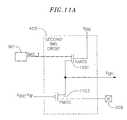
- FIG. 11Ais a schematic diagram of a circuit used to generate V GP1 .
- FIG. 11Bis a schematic diagram illustration of the generation of the V DDO ⁇ V TP voltage depicted in FIG. 11A.
- FIG. 11Cis a graph illustrating the relationship between Bias_Mid and V PAD .
- FIG. 11Dis a schematic diagram depicting an exemplary illustration of a transistor implementation of block 901 .
- FIG. 12Ais a schematic diagram of a circuit that may be used to prevent power on stress of devices, according to an embodiment of the invention.
- FIG. 12Bis a schematic diagram of a circuit that may be used to prevent power on stress of devices, according to another embodiment of the invention.
- FIG. 13is a circuit and block diagram of a portion of an overvoltage protection circuit.
- FIG. 14is a schematic diagram illustrating a modification of FIG. 9A.
- FIG. 15is a schematic diagram illustrating a transistor implementation of block 1401 .
- FIG. 16is a schematic diagram illustrating a transistor implementation of FIG. 14.
- FIG. 17is a schematic diagram of a circuit that may be used to prevent stress on devices when voltage spikes appear at an I/O pad.
- FIG. 18is an embodiment of a circuit including multiple cooperating embodiments, such as those illustrated above.
- FIG. 1is a graphic illustration of an exemplary environment in which embodiments of the invention may be utilized.
- a personal computer systemis represented generally at 101 .
- circuit board 103on which a CPU integrated circuit chip 105 is mounted.
- the CPUis a type which uses 3.3 volts as its supply voltage.
- a keyboard interface integrated circuit chip 107is also mounted on circuit board 103 .
- the keyboard interface integrated circuitis one having a supply voltage of 5.0 volts.
- the CPU 105is coupled to the Keyboard chip 107 .
- the CPU 105may be of a type which contains integrated devices that may be damaged by interfacing with a device having a higher supply voltage. Because of the disparity in supply voltages that may exist in such situations an output circuit which can compensate for the higher interface voltages may be particularly useful.
- FIG. 2is a graphical illustration of a prior art input output circuit and connection.
- a common input output circuitcomprises a pull up device, such as PMOS (P-channel Metal Oxide Semiconductor) device 215 and a pull down device, such as NMOS (N-channel Metal Oxide Semiconductor) device 217 , such as illustrated in FIG. 2.
- Devices 215 and 217are coupled together at an input/output (I/O) pad 219 .
- the substrate for the NMOS deviceis commonly coupled to ground potential, e.g. as shown at 221 .
- the substrate for the NMOS deviceis typically a substrate which is common for the entire integrated circuit chip on which it resides.
- PMOS devicesare commonly fabricated in their own isolated well.
- the component integrated devicescan tolerate only limited differential voltages across their junctions. Commonly the voltage which can be tolerated across the junctions is on the order of 2.5 Volts.
- pad 219interfaces to a volt circuit, and hence the pad may see voltages in the neighborhood of 5.5 volts.
- a 5 volt signal applied to pad 219may stress devices within the chip 105 .
- gate 205 of device 217is at a zero volt potential then the voltage across the 205 - 203 gate-oxide may exceed 5 volts, thereby stressing device 217 .
- more than one devicemay be used to divide the voltages in pull up and pull down I/O circuits.
- FIG. 3is a schematic of a portion of a MOS (Metal Oxide Semiconductor) input output circuit in which each push pull output device illustrated in FIG. 2 has been replaced by two devices. That is output device 215 has been replaced by devices 301 and 303 and device 217 has been replaced by devices 305 and 307 . By replacing devices 215 and 217 by two devices each, the output voltage appearing at pad 309 may be safely divided over the two upper ( 301 and 303 ) and the two lower ( 305 and 307 ) I/O devices.
- the middle NMOS device 303 and the middle PMOS device 305have their gates biased to intermediate potentials to avoid excessive voltages under various pad voltages 309 .
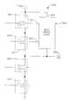
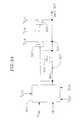
- FIG. 4is input output circuit 404 , including a well biasing circuit, according to an embodiment of the invention.
- Devices 301 and 303are fabricated in wells, illustrated schematically as 400 and 402 , which are essentially at a floating potential. Because devices in wells at floating potential can have problems, such as device latch up, wells are commonly connected to a known bias voltage.
- the wells of devices 301 and 303are tied to the highest circuit potential available using well biasing circuit 401 .
- the inputs to the well biasing circuitare the pad voltage present on input output pad 309 , V DDO and voltage V GP1 , the characteristics of which are illustrated in FIG. 7.
- FIG. 5is a graph illustrating the relationship between well voltage and pad voltage for the I/O circuit in an input (or a tristate) condition. As can be seen from the graph, if the pad voltage is less than V DDO then the well voltage is equal to V DDO . If the pad voltage is greater than V DDO then the well voltage is equal to the pad voltage. The well bias can thereby be changed according to changing circuit conditions.
- FIG. 6is a block diagram of I/O circuitry 600 biasing according to an embodiment of the invention.
- first bias circuit 407couples the gate 403 of device 301 to V DDO .
- device 301is controlled by an input from first bias circuit 407 according to whether V PAD needs to be a high or low value.
- second bias circuit 405provides gate voltage V GP1 to the gate of output device 303 .
- Such biasingprevents device 303 from being damaged due to a voltage potential across its junctions.
- FIG. 7is a graphical representation of V GP1 bias voltage as a function of pad voltage (V PAD ) If V PAD is less than V DDO then V GP1 provided to the gate of output device 303 is equal to the intermediate supply voltage V DDC . If V PAD is greater than V DDO then V GP1 provided to the gate of output device 303 is equal to V PAD . In such a manner the voltage between the gate of device 303 and pad 309 can be kept in a safe range to prevent damage to the junction.
- the well biasing circuit 401ties the wells of devices 301 and 303 to V DDO .
- the gate voltage of the upper NMOS device 305is controlled by third bias circuit 409 .
- Fourth bias circuit 411works in a similar fashion to first bias circuit 407 . Both bias circuits 407 and 411 work in a digital mode, either providing a first or second voltage depending on the required I/O pad 309 output voltage. In a first mode of operation, first bias circuit 407 switches between a first voltage V DDO and a second lower voltage V DDC gate bias circuit 411 switches between providing V DDP and ground potential at the same time to the gate of device 307 .
- FIG. 8is a graphical illustration of a circuit configuration used to provide the pad voltage to the core circuitry.
- the V PAD inputis coupled to the core circuitry 803 through an NMOS device 801 .
- the gate of NMOS device 801accepts Bias_Mid as its control voltage. Such an arrangement protects the gate source voltage of device 801 and also prevents large voltages from the input from being coupled into the core circuitry when it is in the input, (tristate) or output conditions.
- One facet of the I/O systemcomprising devices 301 , 303 , 305 and 307 is that any number of such devices may be added in parallel, in order to provide any level of drive signals needed.
- FIG. 9Ais a schematic diagram illustrating how Bias_Mid voltage is generated.
- Block 901is a switching circuit that switches its Bias — 1 output between voltages VDDO (3.3 Volts nominally in the present embodiment) and V DDC (1.2 Volts nominally in the present embodiment).
- Device 905is a PMOS device as are devices 907 and 909 .
- Device 907turns on when the output is enabled or the V PAD is low.
- Bias_Midis coupled to V DDP .
- outputis not enabled i.e.
- bias — 1V DDO and device 905 charges point 911 to bias — 1 ⁇ V TP , where V TP is the threshold of device 905 , and accordingly is the voltage dropped across device 905 .
- Bias_Mid_V DDP +V TPthen device 909 will drain current from node 911 such that V DDP +V TP is the maximum value for Bias_Mid.
- Bias_Midis always between V DDP +V TP and V DDO ⁇ V TP whether V DDP +V TP or V DDO ⁇ V TP is larger.
- a typical V TPis 0.5 volts.
- the actual value of Bias_Midwill be determined by the relative sizes of devices 907 and 909 .
- FIG. 9Bis a schematic diagram of another embodiment for generation of Bias_Mid voltage.
- Bias_Midis always less than V SSC +nV Tn and greater than V DDO ⁇ kV Tp , where nV Tn is an offset voltage due to device thresholds, for example devices 909 c , 910 c , 911 c and 912 c and kV Tp is also an offset voltage due to device thresholds, for example devices 907 c and 908 c .
- n and kare integers dependent on the number of devices employed.
- FIG. 10is a schematic diagram of an exemplary well biasing circuit, according to an embodiment of the invention.
- Device 1001when turned on, couples pad 309 to well 1005 .
- Device 1003when turned on, couples V DDO to the well 1005 .
- V PADis less than V DDO the gate source of device 1001 is less than the threshold voltage of device 1001 , and device 1001 is turned off.
- V GP1is low (e.g 1.2 Volts) then device 1003 conducts, thereby coupling well 1005 to V DDO .
- V PADis equal to V DDO or greater then device 1001 will begin to turn on, thereby coupling the well 1005 to V PAD .
- FIG. 11Ais a schematic diagram of a circuit used to generate V GP1 .
- Bias 1switches between V DDO (3.3 volts) and VDDC (1.2 volts).
- Device 1101couples Bias — 1 to V GP1 .
- bias — 1is 3.3 volts device 1101 is off and when bias — 1 is 1.2 Volts then V GP1 is tied to 1.2 Volts.
- V PAD at 309is greater than V DDO device 1103 begins to conduct, because the gate of device 1103 is tied to V DDO ⁇ V TP , and V GP1 is thereby coupled to V PAD .
- FIG. 11Bshows a circuit which may be used to generate V DDO ⁇ V TP .
- the strong upper PMOS devicechanges the node 1150 to V DDO ⁇ V TP .
- problems that may be caused when a lower supply voltage chip is interfaced with a higher voltage chipthere are “power on stress” problems, which may be caused when circuitry is turned on and the supplies that provide protective biases are not yet up to their full voltage. In such a case a voltage present at an I/O pad may stress devices which are coupled to that I/O pad.
- FIG. 11Cis a graph illustrating the relationship between Bias_Mid and V PAD .
- Bias_Midis set at 2.5 volts, and remains at 2.5 volts until V PAD increases beyond 2.5 volts. Thereafter Bias_Mid tracks voltage increases at V PAD and becomes equal to a higher voltage when V PAD increases beyond a certain value.
- FIG. 11Dis a schematic diagram depicting an exemplary illustration of a transistor implementation of block 901 .
- FIG. 12Ais a schematic diagram of a circuit that may be used to prevent power on stress of devices, according to an embodiment of the invention.
- the circuit illustrated in FIG. 12Amay be used to generate the Bias_Mid voltage when V DDO is not up to its nominal value. If Bias_Mid is present then devices 305 and 307 , shown in FIG. 8, will be protected from junction overvoltage problems even though the voltages, which ordinarily would be used to generate Bias_Mid as explained in FIG. 9A, are not present.
- devices 1201 , 1203 , and 1205are arranged as a series of diode connected transistors such that a threshold voltage V TP (in the present example equal to approximately 0.5 volts) is dropped across each device when it is conducting.
- V TPin the present example equal to approximately 0.5 volts
- the pad voltage, minus the threshold voltage of devices 1201 , 1203 , 1205 and 1207is connected to Bias_Mid.
- Device 1207in essence, acts as a switch.
- V DDOis initially zero volts.
- Zero volts at the gate of device 1209turns it on.
- point 1211charges to a potential close to the pad voltage, since device 1213 is off.
- Point 1211is connected to the gate of device 1214 thereby turning device 1214 off.
- PMOS device 1219turns on, which causes the gate of device 1207 to be coupled to Bias_Mid.
- Bias_MidWhen the gate of device 1207 is coupled to Bias_Mid, device 1207 turns on.
- Device 1207 turning oncouples V PAD minus the threshold voltage of devices 1201 , 1203 , 1205 and 1207 to Bias_Mid.
- V DDOWhen V DDO is low, device 1215 provides a current leakage path for Bias_Mid to V DDC or V DDP .
- V DDOWhen V DDO is low, the string of devices 1217 turns on and the pad voltage is coupled to Bias_Mid.
- Devices 1220 , 1221 , 1223 and 1225act as protection for device 1209 in the instance where the V PAD is high and V DDO is low.
- V DDOWhen V DDO is high, point 1211 is tied to Bias_Mid because device 1213 turns on.
- V DDOWhen V DDO is high, device 1219 is turned off and device 1213 is turned on, thus raising the potential at the base of device 1207 to V PAD , thereby turning device 1207 off. Also device 1215 turns off when V DDO is high.
- FIG. 12Bis a modification of the circuitry illustrated in FIG. 12A.
- the circuitry of FIG. 12Bmay also be used to prevent power on stress of devices.
- NMOSN-channel Semiconductor
- Transistors 1251 , 1252 , and 1253limit the maximum value of Bias_Mid to approximately V B +3V Tn where V B is the voltage of node B and V Tn is the threshold voltage of transistors 1251 , 1252 , and 1253 .
- Bias_MidIn general if there are n NMOS transistors similarly connected in series, the maximum value of Bias_Mid is approximately V B +3V Tn . Node B alternatively could b coupled to a power supply voltage such as V DDP , V DDC or V SSC .
- the minimum value of Bias_Midis approximately V pad ⁇ 4V Tp , where V Tp is the threshold voltage of transistors 1201 , 1203 , 1205 , 1207 .
- FIG. 13is a circuit and block diagram of a portion of an over voltage protection circuit.
- Device 1001provides a protection mechanism for the well bias. If V DDO is lower than the pad voltage by V TP or more then device 1001 will turn on. If device 1001 turns on then the well is coupled, via device 1001 , to the pad, and hence the well will be biased to V PAD .
- device 1301is coupled between the pad and P_Gate, the gate of PMOS device 303 shown in FIG. 6.
- the gate of device 1301is biased so that when V DDO is lower than the pad voltage by V Tp or more, then device 1301 will turn on and couple P_Gate to the pad voltage, therefore if V DDO is low then P_Gate will not depend on V DDO for it's voltage level and instead will take the voltage level from the voltage on the pad.
- FIG. 14is a schematic diagram illustrating a modification of FIG. 9A.
- block 901is decoupled from the Bias_Mid signal when V DDO is lower than its nominal value. The decoupling is done using block 1401 .
- the node V_pwris decoupled from V DDP by using block 1401 as a switch.
- the node V_pwris coupled to V DDP by using block 1401 .
- FIG. 15is a schematic diagram illustrating a transistor implementation of block 1401 .
- V DDOis greater than a certain value
- NMOS 1507is turned on thereby connecting the gate of PMOS 1505 to V DDC .
- Connecting the gate of PMOS 1505 to V DDCturns on 1505 thereby connecting V_pwr to V DDP .
- V DDOis less than a certain value
- NMOS 1507is turned off and PMOS 1506 is turned on thereby connecting the gate of PMOS 1505 to Bias_Mid, thereby turning off PMOS 1505 and disconnecting V_pwr from V DDP .
- FIG. 16is a schematic diagram illustrating a transistor implementation of FIG. 14.
- FIG. 17is a schematic diagram of a circuit that may be used to prevent stress on devices when voltage spikes appear at the pad.
- the Bias_Mid voltagechanges momentarily due to the gate to drain overlap capacitance (Cgd) of the driver NMOS.
- FIG. 18is an embodiment of a circuit including multiple cooperating embodiments, such as those illustrated previously.
- the I/O circuit of FIG. 18employs 2.5 volt transistors, with an output voltage of 3.3 volts and a maximum input voltage of 5.5 Volts.
- V DDOWhen V DDO is above a predetermined value, for example 2.5 volts, and the I/O pad 1800 is enabled in an output mode (for example output enable signal OE is high). Under these conditions the maximum pad voltage is V DDO .
- V GP1(the gate of PMOS device 303 ) is coupled to V DDC through NMOS transistors 1101 and 1801 , and accordingly PMOS 303 and PMOS 1505 are turned on.
- Block 901generates an output Bias — 1 voltage of V DDC .
- PMOS 907is turned-on in this condition, Bias_Mid has a steady state value of V DDP and PMOS 905 is turned off.
- V DDOWhen V DDO is below a predetermined value (in the present example 2.5 volts) and I/O pad 1800 is output enabled (i.e. OE is high) then V GP1 , the gate of PMOS device 303 , is floating. Additionally PMOS device 1505 is turned-off and hence Bias_Mid is decoupled from V DDP . PMOS devices 1201 , 1203 and 1207 are turned on.
- the Bias_Mid steady-state voltageis between V PAD ⁇ kV Tp and V SSC +nV t where kV TP and nV t are offset voltages due to the threshold voltages of PMOS semiconductor devices 1201 , 1203 , 1207 and NMOS semiconductor devices 909 c , 910 c , 911 c and 912 c respectively.
- k and nare integers reflecting a number of devices.
- V DDOWhen V DDO is above a pre-determined value, for example 2.5 volts, and when the I/O pad is in an output disabled condition (i.e. OE is low) and the pad voltage is below the predetermined voltage, for example 2.5 volts, then the following circuit conditions are present.
- PMOS device 1505is turned on.
- Block 901generates an output, Bias — 1, voltage of V DDC , accordingly PMOS device 907 is turned-on and the steady state voltage of Bias_Mid is V DDP .
- PMOS 905is turned off under these conditions.
- V GP1(at the gate of PMOS device 303 ) is connected to the pad voltage, if V PAD is greater than V DDO otherwise V GP1 is floating.
- Block 901When V DDO is above a pre-determined value, for example 2.5 volts, and when the I/O pad is in an output disabled condition (i.e. OE is low) and the pad voltage is above the predetermined voltage, for example 2.5 volts, then the following circuit conditions are present.
- Block 901generates an output Bias — 1 voltage of VDDO. Accordingly PMOS device 907 is turned off, PMOS device 905 is turned on and the steady state Bias_Mid voltage is between V DDO ⁇ V DDP , as a minimum value, and V SSC +nV T , as a maximum value.
- nV Tis an offset voltage due to the threshold values of NMOS devices 909 c , 910 c , 911 c and 912 c .
- V GP1the gate of PMOS 303 , is coupled to the pad voltage, V PAD , if V PAD is greater than V DDO .
- V DDOWhen V DDO is below a pre-determined value, for example 2.5 volts, and when the I/O pad is in an output disabled condition (i.e. OE is low), then the following circuit conditions are present.
- PMOS device 1505is turned-off and hence Bias_Mid is disconnected from V DDP .
- PMOS devices 1201 , 1203 , and 1207are turned on.
- the steady state value of the Bias_Mid voltageis between V PAD ⁇ kV TP and V SSC +nV t , where kV Tp and nV t are offset voltages due to the threshold voltages of PMOS devices 1201 , 1203 , 1207 and NMOS devices 909 c , 910 c , 911 c , and 912 c .
- V GP1at the gate of PMOS device 303 is coupled to the pad voltage (V PAD ) if V PAD is greater than V DDO . Under these conditions PMOS device 303 is turned off.
- Capacitors C bm and C gp in FIG. 18are used to insure that Bias_Mid voltage and V GP1 voltage, respectively, are kept at desirable levels when transient voltages appear at the pad as described with respect to FIG. 17.
Landscapes
- Engineering & Computer Science (AREA)
- Computer Hardware Design (AREA)
- Physics & Mathematics (AREA)
- Computing Systems (AREA)
- General Engineering & Computer Science (AREA)
- Mathematical Physics (AREA)
- Power Engineering (AREA)
- Semiconductor Integrated Circuits (AREA)
- Logic Circuits (AREA)
- Metal-Oxide And Bipolar Metal-Oxide Semiconductor Integrated Circuits (AREA)
- Amplifiers (AREA)
Abstract
Description
- This application claims priority from provisional application No. 60/260,582 entitled “Sub-Micron, high input voltage tolerant I/O circuit” filed Jan. 9, 2001, which is hereby incorporated by reference as though set forth in full.[0001]
- This application also claims priority from provisional application No. 60/260,580 entitled “Sub-Micron, high input voltage tolerant I/O circuit with power management support” filed Jan. 9, 2001, which is hereby incorporated by reference as though set forth in full.[0002]
- The present invention relates to integrated circuits (ICs), such as interface circuits, that are designed having reduced feature sizes, for example, 0.13 μm. More particularly, the invention relates to ICs that include interfaces (such as input/output (I/O) circuits) that are capable of interfacing with comparatively high-voltage signals from other sources, for example a 3.3 volt IC interfacing with signals from a 5 volt IC, or any other disparate ranges. Moreover, the invention relates to integrated circuits in which the semiconductor devices are biased such that the stress across the gate-oxides and junctions, as well as the leakage currents, are maintained at tolerable levels.[0003]
- The trend in CMOS-based processing technology is to produce integrated circuit (IC) cores having a higher density of semiconductor devices, such as transistors, and faster clock rates than their predecessors. I/O signals, which electrically connect the IC core to external components, are accessed through I/O circuit pads that surround the IC core. The IC core and the I/O circuit pads are generally fabricated from the same processing technology. There is however no requirement that they comprise the same technology and hybrid circuits are known in the art. The inventive concepts herein are applicable to a variety of fabrication technologies.[0004]
- The performance of the IC cores may generally be improved by shrinking the feature sizes of the semiconductor devices, for example field-effect transistors (FETs). Unfortunately, reducing the IC feature sizes may proportionally decrease the maximum operating voltage that the semiconductor devices within the IC can withstand. For example, an I/O circuit pad, fabricated from a CMOS process having 0.30 micron features, typically withstands a maximum operating voltage of about 3.6 volts. In such a case the maximum operating voltage of the I/O circuit pad is insufficient to drive the external components which have a higher voltage requirement, such as 5 volts. Furthermore, if the IC is interfaced with a greater than the maximum operating voltage, the IC may fail.[0005]
- One way to attempt to resolve the requirements of circuits with mismatched voltage requirements is to increase the robustness of the fabrication process, for example by increasing the thickness of the gate-oxide layer of the semiconductor devices which comprise the IC circuitry. A thick gate-oxide layer may provide semiconductor devices, such as FETs, with the ability to support a higher voltage requirement. However, this voltage robustness is commonly accompanied by a decreases the performance of the IC, because the thick gate-oxide layer reduces the overall gain of the devices which comprise the IC. Reducing the gain minimizes the benefit which occurs by reducing the feature size.[0006]
- Other attempts have included increasing the complexity of the CMOS fabrication process so there are multiple sets of devices where each set meets different voltage requirements. Each set of devices requires a different gate-oxide. Each additional gate-oxide requires a separate mask. The resulting hybrid process may significantly increase the manufacturing costs of the IC.[0007]
- One way to avoid the drawbacks of the aforementioned processing-based solutions is to use a “level-shift” chip as an external component. The IC core and the I/O circuits are fabricated from the same process. The “level-shift chip” may be fabricated from a process that supports the discrete voltage requirement by stepping up the core output signals to support the discrete voltage range and stepping down the external drive signals to support the IC core voltage range. Such a level-shift chip can be a waste of much needed space on a crowded printed circuit board and may degrade performance.[0008]
- An I/O circuit that transforms voltages between different voltage levels without degrading the overall performance of the integrated circuit and maximizing use of space on the printed circuit board or multi-chip substrate may be beneficial. It would be a further benefit if such an I/O circuit could use voltages presented at the I/O circuit in order to provide such protective biasing.[0009]
- Commonly an I/O power supply may vary +/−10% and may vary significantly more during transient conditions. An I/O power supply may even go to zero at power off. When the I/O power supply varies, circuits may have higher stress on the gate-oxides of the devices in the I/O circuit, such stresses may not be desirable in many process technologies. It may be desirable to provide bias voltages to various devices in the I/O circuit such that the device gate-oxide is protected from high-voltages under various conditions of operation even when the power-supply voltage varies by a large amount.[0010]
- Embodiments of the present invention may be optimized, for example where 5 volt input tolerance is required, even when the power supplies are varying by a significant amount, which may range from a maximum value to zero.[0011]
- Embodiments of the present invention are illustrated in an optimized form for I/O circuits where a 5 volt +/−10% input tolerance is required for normal operating range. Additionally the inventive concepts herein are described in terms of CMOS (Complimentary Metal Oxide Semiconductor) integrated circuits. Those skilled in the art will readily appreciate the fact that techniques described with respect to CMOS ICs are readily applicable to any circuits having disparate power supply and/or drive signal requirements for different portions of the circuitry. The CMOS example chosen is one likely to be familiar to those skilled in the art. There is, however, no intent to limit the inventive concepts to CMOS ICs as the techniques are equally applicable to a wide variety of integrated circuit fabrication techniques.[0012]
- An exemplary embodiment of the invention includes an integrated circuit having a four device input output circuit in a push pull configuration. Two of the devices, termed upper devices, comprise PMOS (P-Channel Metal Oxide Semiconductor) devices and two of the devices, termed lower devices, comprise NMOS (N-channel Metal Oxide Semiconductor) devices. The devices are biased to reduce hazardous voltages across device junctions and to eliminate the magnitude of the voltage being passed on to the core circuitry. The biases are derived from the input output state of the circuit and the voltage presented to the I/O circuit connection (V[0013]PAD), and the variation of supply voltages. Additionally PMOS device well bias voltage is developed based on VPADand power supply voltage.
- Other features and advantages of the invention will become apparent from a description of the following figures, in which like numbers refer to similar items throughout.[0014]
- FIG. 1 is a graphic illustration of an exemplary environment in which embodiments of the invention may be utilized.[0015]
- FIG. 2 is a graphical illustration of a prior art input output circuit and connection to a circuit having a different power supply voltage.[0016]
- FIG. 3 is a schematic of a portion of a MOS (Metal Oxide Semiconductor) input output circuit in which single push and pull output devices have been replaced by two devices each.[0017]
- FIG. 4 is input output circuit, including a well biasing circuit, according to an embodiment of the invention.[0018]
- FIG. 5 is a graph illustrating the relationship between well voltage and pad voltage for the input (or a tristate) mode, according to an embodiment of the invention.[0019]
- FIG. 6 is a block diagram of I/O circuitry biasing according to an embodiment of the invention.[0020]
- FIG. 7 is a graphical representation of V[0021]GP1bias voltage as a function of pad voltage (VPAD)
- FIG. 8 is a graphical illustration of a circuit configuration used to provide the pad voltage to integrated circuit core circuitry.[0022]
- FIG. 9A is a schematic diagram of an embodiment to generate a Bias_Mid voltage, according to an embodiment of the invention.[0023]
- FIG. 9B is a schematic diagram of an alternate embodiment to generate a Bias_Mid voltage, according to an embodiment of the invention.[0024]
- FIG. 10 is a schematic diagram of an exemplary well biasing circuit, according to an embodiment of the invention.[0025]
- FIG. 11A is a schematic diagram of a circuit used to generate V[0026]GP1.
- FIG. 11B is a schematic diagram illustration of the generation of the V[0027]DDO−VTPvoltage depicted in FIG. 11A.
- FIG. 11C is a graph illustrating the relationship between Bias_Mid and V[0028]PAD.
- FIG. 11D is a schematic diagram depicting an exemplary illustration of a transistor implementation of[0029]
block 901. - FIG. 12A is a schematic diagram of a circuit that may be used to prevent power on stress of devices, according to an embodiment of the invention.[0030]
- FIG. 12B is a schematic diagram of a circuit that may be used to prevent power on stress of devices, according to another embodiment of the invention.[0031]
- FIG. 13 is a circuit and block diagram of a portion of an overvoltage protection circuit.[0032]
- FIG. 14 is a schematic diagram illustrating a modification of FIG. 9A.[0033]
- FIG. 15 is a schematic diagram illustrating a transistor implementation of[0034]
block 1401. - FIG. 16 is a schematic diagram illustrating a transistor implementation of FIG. 14.[0035]
- FIG. 17 is a schematic diagram of a circuit that may be used to prevent stress on devices when voltage spikes appear at an I/O pad.[0036]
- FIG. 18 is an embodiment of a circuit including multiple cooperating embodiments, such as those illustrated above.[0037]
- FIG. 1 is a graphic illustration of an exemplary environment in which embodiments of the invention may be utilized. In FIG. 1 a personal computer system is represented generally at[0038]101. Within the computer system is
circuit board 103 on which a CPU integratedcircuit chip 105 is mounted. The CPU is a type which uses 3.3 volts as its supply voltage. A keyboard interface integratedcircuit chip 107 is also mounted oncircuit board 103. The keyboard interface integrated circuit is one having a supply voltage of 5.0 volts. TheCPU 105 is coupled to theKeyboard chip 107. TheCPU 105 may be of a type which contains integrated devices that may be damaged by interfacing with a device having a higher supply voltage. Because of the disparity in supply voltages that may exist in such situations an output circuit which can compensate for the higher interface voltages may be particularly useful. - FIG. 2 is a graphical illustration of a prior art input output circuit and connection. A common input output circuit comprises a pull up device, such as PMOS (P-channel Metal Oxide Semiconductor)[0039]
device 215 and a pull down device, such as NMOS (N-channel Metal Oxide Semiconductor)device 217, such as illustrated in FIG. 2.Devices pad 219. The substrate for the NMOS device is commonly coupled to ground potential, e.g. as shown at221. The substrate for the NMOS device is typically a substrate which is common for the entire integrated circuit chip on which it resides. PMOS devices are commonly fabricated in their own isolated well. - In deep submicron fabrication, the component integrated devices can tolerate only limited differential voltages across their junctions. Commonly the voltage which can be tolerated across the junctions is on the order of 2.5 Volts.[0040]
- In the Illustration of FIG. 2[0041]
pad 219 interfaces to a volt circuit, and hence the pad may see voltages in the neighborhood of 5.5 volts. A 5 volt signal applied to pad219 may stress devices within thechip 105. For example if gate205 ofdevice 217 is at a zero volt potential then the voltage across the205-203 gate-oxide may exceed 5 volts, thereby stressingdevice 217. For this reason more than one device may be used to divide the voltages in pull up and pull down I/O circuits. - FIG. 3 is a schematic of a portion of a MOS (Metal Oxide Semiconductor) input output circuit in which each push pull output device illustrated in FIG. 2 has been replaced by two devices. That is[0042]
output device 215 has been replaced bydevices device 217 has been replaced bydevices devices pad 309 may be safely divided over the two upper (301 and303) and the two lower (305 and307) I/O devices. Themiddle NMOS device 303 and themiddle PMOS device 305 have their gates biased to intermediate potentials to avoid excessive voltages undervarious pad voltages 309. - FIG. 4 is[0043]
input output circuit 404, including a well biasing circuit, according to an embodiment of the invention.Devices devices circuit 401. The inputs to the well biasing circuit are the pad voltage present oninput output pad 309, VDDOand voltage VGP1, the characteristics of which are illustrated in FIG. 7. - During the operation of I/[0044]
O circuit 404 in an output mode (i.e. whenpad 309 is in an output mode),wells pad 309 is in an input mode, the well voltage depends upon the pad voltage. In the output mode Vwell=VDDO. - When I/[0045]
O circuit 404 is in an input mode (whenpad 309 is in an input mode), Vwelldepends on both the input (Pad) voltage VPADas well as VDDO. If VPADis less than VDDO, wheninput output circuit 404 in the input or tristate mode, then Vwell=VDDO. If VPADis greater than VDDO, wheninput output circuit 404 in the input or tristate mode, then Vwell=VPAD. A graph of this relationship is illustrated in FIG. 5. - FIG. 5 is a graph illustrating the relationship between well voltage and pad voltage for the I/O circuit in an input (or a tristate) condition. As can be seen from the graph, if the pad voltage is less than V[0046]DDOthen the well voltage is equal to VDDO. If the pad voltage is greater than VDDOthen the well voltage is equal to the pad voltage. The well bias can thereby be changed according to changing circuit conditions.
- FIG. 6 is a block diagram of I/[0047]
O circuitry 600 biasing according to an embodiment of the invention. - When I/[0048]
O circuitry 600 is in the input mode,first bias circuit 407 couples thegate 403 ofdevice 301 to VDDO. In the output mode,device 301 is controlled by an input fromfirst bias circuit 407 according to whether VPADneeds to be a high or low value. - In the input mode[0049]
second bias circuit 405 provides gate voltage VGP1to the gate ofoutput device 303. The gate voltage VGP1provided to the gate ofoutput device 303 varies from an intermediate power supply voltage, such as VDDC=1.2 volts, and the pad voltage presented to the circuit atinput output pad 309. Such biasing preventsdevice 303 from being damaged due to a voltage potential across its junctions. - FIG. 7 is a graphical representation of V[0050]GP1bias voltage as a function of pad voltage (VPAD) If VPADis less than VDDOthen VGP1provided to the gate of
output device 303 is equal to the intermediate supply voltage VDDC. If VPADis greater than VDDOthen VGP1provided to the gate ofoutput device 303 is equal to VPAD. In such a manner the voltage between the gate ofdevice 303 and pad309 can be kept in a safe range to prevent damage to the junction. - To summarize the operation of the circuit of FIG. 6, when the[0051]
circuit 600 is in an output mode: Thewell biasing circuit 401 ties the wells ofdevices lower PMOS device 307 is tied to an intermediate voltage, such as VDDC=1.2 Volts. The gate ofupper NMOS device 305 is tied to an intermediate voltage, such as VDDP=2.5 Volts. - When the[0052]
circuit 600 is in not in output mode, that is in the tri-state or input mode thenupper PMOS device 301 andlower NMOS device 307 are turned off anddevices - The gate voltage of the[0053]
upper NMOS device 305 is controlled bythird bias circuit 409.Third bias circuit 409, when in an input or tristate mode, will increase the Bias_Mid voltage when the pad voltage increases beyond a certain threshold, for example VDDP=2.5 Volts. - [0054]
Fourth bias circuit 411 works in a similar fashion tofirst bias circuit 407. Both biascircuits O pad 309 output voltage. In a first mode of operation,first bias circuit 407 switches between a first voltage VDDOand a second lower voltage VDDCgate bias circuit 411 switches between providing VDDPand ground potential at the same time to the gate ofdevice 307. - FIG. 8 is a graphical illustration of a circuit configuration used to provide the pad voltage to the core circuitry. The V[0055]PADinput is coupled to the
core circuitry 803 through anNMOS device 801. The gate ofNMOS device 801 accepts Bias_Mid as its control voltage. Such an arrangement protects the gate source voltage ofdevice 801 and also prevents large voltages from the input from being coupled into the core circuitry when it is in the input, (tristate) or output conditions. - One facet of the I/O[0056]
system comprising devices - FIG. 9A is a schematic diagram illustrating how Bias_Mid voltage is generated.[0057]
Block 901 is a switching circuit that switches itsBias —1 output between voltages VDDO (3.3 Volts nominally in the present embodiment) and VDDC(1.2 Volts nominally in the present embodiment).Device 905 is a PMOS device as aredevices Device 907 turns on when the output is enabled or the VPADis low. Whendevice 907 is turned on, Bias_Mid is coupled to VDDP. When output is not enabled i.e. the pad is in the tri-state (input only) mode and VPADis high, then bias—1=VDDOanddevice 905 charges point911 tobias —1−VTP, where VTPis the threshold ofdevice 905, and accordingly is the voltage dropped acrossdevice 905. If Bias_Mid_VDDP+VTPthendevice 909 will drain current fromnode 911 such that VDDP+VTPis the maximum value for Bias_Mid. Bias_Mid is always between VDDP+VTPand VDDO−VTPwhether VDDP+VTPor VDDO−VTPis larger. A typical VTPis 0.5 volts. The actual value of Bias_Mid will be determined by the relative sizes ofdevices - FIG. 9B is a schematic diagram of another embodiment for generation of Bias_Mid voltage. In FIG. 9B Bias_Mid is always less than V[0058]SSC+nVTnand greater than VDDO−kVTp, where nVTnis an offset voltage due to device thresholds, for example devices909c,910c,911cand912cand kVTpis also an offset voltage due to device thresholds, for example devices907cand908c. Where n and k are integers dependent on the number of devices employed.
- FIG. 10 is a schematic diagram of an exemplary well biasing circuit, according to an embodiment of the invention.[0059]
Device 1001, when turned on, couples pad309 to well1005.Device 1003, when turned on, couples VDDOto thewell 1005. When VPADis less than VDDOthe gate source ofdevice 1001 is less than the threshold voltage ofdevice 1001, anddevice 1001 is turned off. When VGP1is low (e.g 1.2 Volts) thendevice 1003 conducts, thereby coupling well1005 to VDDO. When VPADis equal to VDDOor greater thendevice 1001 will begin to turn on, thereby coupling the well1005 to VPAD. - FIG. 11A is a schematic diagram of a circuit used to generate V[0060]GP1. Bias1 switches between VDDO(3.3 volts) and VDDC (1.2 volts).
Device 1101 couples Bias—1 to VGP1. Whenbias —1 is 3.3volts device 1101 is off and whenbias —1 is 1.2 Volts then VGP1is tied to 1.2 Volts. When the VPADat309 is greater than VDDOdevice1103 begins to conduct, because the gate ofdevice 1103 is tied to VDDO−VTP, and VGP1is thereby coupled to VPAD. - FIG. 11B shows a circuit which may be used to generate V[0061]DDO−VTP. The strong upper PMOS device changes the node1150 to VDDO−VTP. In addition to the problems that may be caused when a lower supply voltage chip is interfaced with a higher voltage chip there are “power on stress” problems, which may be caused when circuitry is turned on and the supplies that provide protective biases are not yet up to their full voltage. In such a case a voltage present at an I/O pad may stress devices which are coupled to that I/O pad.
- FIG. 11C is a graph illustrating the relationship between Bias_Mid and V[0062]PAD. Bias_Mid is set at 2.5 volts, and remains at 2.5 volts until VPADincreases beyond 2.5 volts. Thereafter Bias_Mid tracks voltage increases at VPADand becomes equal to a higher voltage when VPADincreases beyond a certain value.
- FIG. 11D is a schematic diagram depicting an exemplary illustration of a transistor implementation of[0063]
block 901. - FIG. 12A is a schematic diagram of a circuit that may be used to prevent power on stress of devices, according to an embodiment of the invention. The circuit illustrated in FIG. 12A may be used to generate the Bias_Mid voltage when V[0064]DDOis not up to its nominal value. If Bias_Mid is present then
devices - In FIG.[0065]
12A devices device 1207 is conducting, the pad voltage, minus the threshold voltage ofdevices Device 1207, in essence, acts as a switch. - As an example, assume that V[0066]DDOis initially zero volts. Zero volts at the gate of
device 1209 turns it on. Insuch case point 1211 charges to a potential close to the pad voltage, sincedevice 1213 is off.Point 1211 is connected to the gate ofdevice 1214 thereby turningdevice 1214 off. Since VDDOis zero volts,PMOS device 1219 turns on, which causes the gate ofdevice 1207 to be coupled to Bias_Mid. When the gate ofdevice 1207 is coupled to Bias_Mid,device 1207 turns on.Device 1207 turning on couples VPADminus the threshold voltage ofdevices device 1215 provides a current leakage path for Bias_Mid to VDDCor VDDP. When VDDOis low, the string ofdevices 1217 turns on and the pad voltage is coupled to Bias_Mid.Devices device 1209 in the instance where the VPADis high and VDDOis low. - When V[0067]DDOis high,
point 1211 is tied to Bias_Mid becausedevice 1213 turns on. When VDDOis high,device 1219 is turned off anddevice 1213 is turned on, thus raising the potential at the base ofdevice 1207 to VPAD, thereby turningdevice 1207 off. Alsodevice 1215 turns off when VDDOis high. - FIG. 12B is a modification of the circuitry illustrated in FIG. 12A. The circuitry of FIG. 12B may also be used to prevent power on stress of devices. In FIG. 12B NMOS (N-channel Semiconductor)[0068]
transistors 1251,1252, and1253 are added between Bias_Mid and node B,1255.Transistors 1251,1252, and1253 limit the maximum value of Bias_Mid to approximately VB+3VTnwhere VBis the voltage of node B and VTnis the threshold voltage oftransistors 1251,1252, and1253. In general if there are n NMOS transistors similarly connected in series, the maximum value of Bias_Mid is approximately VB+3VTn. Node B alternatively could b coupled to a power supply voltage such as VDDP, VDDCor VSSC. The minimum value of Bias_Mid is approximately Vpad−4VTp, where VTpis the threshold voltage oftransistors - FIG. 13 is a circuit and block diagram of a portion of an over voltage protection circuit.[0069]
Device 1001 provides a protection mechanism for the well bias. If VDDOis lower than the pad voltage by VTPor more thendevice 1001 will turn on. Ifdevice 1001 turns on then the well is coupled, viadevice 1001, to the pad, and hence the well will be biased to VPAD. - Similarly[0070]
device 1301 is coupled between the pad and P_Gate, the gate ofPMOS device 303 shown in FIG. 6. The gate ofdevice 1301 is biased so that when VDDOis lower than the pad voltage by VTpor more, thendevice 1301 will turn on and couple P_Gate to the pad voltage, therefore if VDDOis low then P_Gate will not depend on VDDOfor it's voltage level and instead will take the voltage level from the voltage on the pad. - FIG. 14 is a schematic diagram illustrating a modification of FIG. 9A. In FIG. 14[0071]
block 901 is decoupled from the Bias_Mid signal when VDDOis lower than its nominal value. The decoupling is done usingblock 1401. When VDDOis not up to its nominal value, the node V_pwr is decoupled from VDDPby usingblock 1401 as a switch. When VDDOis up to its nominal value, the node V_pwr is coupled to VDDPby usingblock 1401. - FIG. 15 is a schematic diagram illustrating a transistor implementation of[0072]
block 1401. When VDDOis greater than a certain value,NMOS 1507 is turned on thereby connecting the gate ofPMOS 1505 to VDDC. Connecting the gate ofPMOS 1505 to VDDCturns on1505 thereby connecting V_pwr to VDDP. When VDDOis less than a certain value,NMOS 1507 is turned off andPMOS 1506 is turned on thereby connecting the gate ofPMOS 1505 to Bias_Mid, thereby turning offPMOS 1505 and disconnecting V_pwr from VDDP. - FIG. 16 is a schematic diagram illustrating a transistor implementation of FIG. 14.[0073]
- FIG. 17 is a schematic diagram of a circuit that may be used to prevent stress on devices when voltage spikes appear at the pad. When transient voltages appear, the Bias_Mid voltage changes momentarily due to the gate to drain overlap capacitance (Cgd) of the driver NMOS. A capacitance (Cbm) is placed at the bias_mid node such that the transient voltage at the pad (V_pad, transient) gets divided between Cgd and Cbm depending on the ratio of the capacitances which gives the additional transient voltage on bias_mid (V_bm, transient): ΔV_bm, transient=(Cgd/(Cgd+Cbm)*ΔV_pad, transient Also, when transient voltages appear, the voltage V[0074]GP1on
PMOS 207 gate changes momentarily due to the gate to drain overlap capacitance (Cgdp) of the driver PMOS. A capacitance (Cgp) is placed at thePMOS 207 gate node such that the transient voltage at the pad (V_pad, transient) gets divided between Cgdp and Cgp depending on the ratio of the capacitances which gives the additional transient voltage onPMOS 207 gate (VGP1+Transient): VGP1+Transient=(Cgdp/(Cgdp+Cgp))*ΔV_pad, transient. - FIG. 18 is an embodiment of a circuit including multiple cooperating embodiments, such as those illustrated previously. The I/O circuit of FIG. 18 employs 2.5 volt transistors, with an output voltage of 3.3 volts and a maximum input voltage of 5.5 Volts. The power supply voltages illustrated are V[0075]DDO=3.3 volts, VDDP=2.5 volts, VDDC=1.2 volts, VSSOis 0 volts and VSSCis 0 volts. The functioning of the circuit is described below.
- When V[0076]DDOis above a predetermined value, for example 2.5 volts, and the I/
O pad 1800 is enabled in an output mode (for example output enable signal OE is high). Under these conditions the maximum pad voltage is VDDO. VGP1(the gate of PMOS device303) is coupled to VDDCthroughNMOS transistors 1101 and1801, and accordinglyPMOS 303 andPMOS 1505 are turned on.Block 901 generates anoutput Bias —1 voltage of VDDC. PMOS907 is turned-on in this condition, Bias_Mid has a steady state value of VDDPandPMOS 905 is turned off. - When V[0077]DDOis below a predetermined value (in the present example 2.5 volts) and I/
O pad 1800 is output enabled (i.e. OE is high) then VGP1, the gate ofPMOS device 303, is floating. AdditionallyPMOS device 1505 is turned-off and hence Bias_Mid is decoupled from VDDP. PMOS devices1201,1203 and1207 are turned on. Therefore the Bias_Mid steady-state voltage is between VPAD−kVTpand VSSC+nVtwhere kVTPand nVtare offset voltages due to the threshold voltages ofPMOS semiconductor devices - When V[0078]DDOis above a pre-determined value, for example 2.5 volts, and when the I/O pad is in an output disabled condition (i.e. OE is low) and the pad voltage is below the predetermined voltage, for example 2.5 volts, then the following circuit conditions are present.
PMOS device 1505 is turned on.Block 901 generates an output,Bias —1, voltage of VDDC, accordinglyPMOS device 907 is turned-on and the steady state voltage of Bias_Mid is VDDP. PMOS905 is turned off under these conditions. VGP1(at the gate of PMOS device303) is connected to the pad voltage, if VPADis greater than VDDOotherwise VGP1is floating. - When V[0079]DDOis above a pre-determined value, for example 2.5 volts, and when the I/O pad is in an output disabled condition (i.e. OE is low) and the pad voltage is above the predetermined voltage, for example 2.5 volts, then the following circuit conditions are present.
Block 901 generates anoutput Bias —1 voltage of VDDO. AccordinglyPMOS device 907 is turned off,PMOS device 905 is turned on and the steady state Bias_Mid voltage is between VDDO−VDDP, as a minimum value, and VSSC+nVT, as a maximum value. The value nVTis an offset voltage due to the threshold values of NMOS devices909c,910c,911cand912c. VGP1the gate ofPMOS 303, is coupled to the pad voltage, VPAD, if VPADis greater than VDDO. - When V[0080]DDOis below a pre-determined value, for example 2.5 volts, and when the I/O pad is in an output disabled condition (i.e. OE is low), then the following circuit conditions are present.
PMOS device 1505 is turned-off and hence Bias_Mid is disconnected from VDDP. PMOS devices1201,1203, and1207 are turned on. The steady state value of the Bias_Mid voltage is between VPAD−kVTPand VSSC+nVt, where kVTpand nVtare offset voltages due to the threshold voltages ofPMOS devices PMOS device 303 is coupled to the pad voltage (VPAD) if VPADis greater than VDDO. Under theseconditions PMOS device 303 is turned off. - Capacitors C[0081]bmand Cgpin FIG. 18 are used to insure that Bias_Mid voltage and VGP1voltage, respectively, are kept at desirable levels when transient voltages appear at the pad as described with respect to FIG. 17.
Claims (22)
Priority Applications (2)
| Application Number | Priority Date | Filing Date | Title |
|---|---|---|---|
| US10/043,763US6847248B2 (en) | 2001-01-09 | 2002-01-09 | Sub-micron high input voltage tolerant input output (I/O) circuit which accommodates large power supply variations |
| US11/001,975US7138847B2 (en) | 2001-01-09 | 2004-12-02 | Sub-micron high input voltage tolerant input output (I/O) circuit which accommodates large power supply variations |
Applications Claiming Priority (3)
| Application Number | Priority Date | Filing Date | Title |
|---|---|---|---|
| US26058201P | 2001-01-09 | 2001-01-09 | |
| US26058001P | 2001-01-09 | 2001-01-09 | |
| US10/043,763US6847248B2 (en) | 2001-01-09 | 2002-01-09 | Sub-micron high input voltage tolerant input output (I/O) circuit which accommodates large power supply variations |
Related Child Applications (1)
| Application Number | Title | Priority Date | Filing Date |
|---|---|---|---|
| US11/001,975ContinuationUS7138847B2 (en) | 2001-01-09 | 2004-12-02 | Sub-micron high input voltage tolerant input output (I/O) circuit which accommodates large power supply variations |
Publications (2)
| Publication Number | Publication Date |
|---|---|
| US20020175743A1true US20020175743A1 (en) | 2002-11-28 |
| US6847248B2 US6847248B2 (en) | 2005-01-25 |
Family
ID=26948078
Family Applications (10)
| Application Number | Title | Priority Date | Filing Date |
|---|---|---|---|
| US10/043,763Expired - Fee RelatedUS6847248B2 (en) | 2001-01-09 | 2002-01-09 | Sub-micron high input voltage tolerant input output (I/O) circuit which accommodates large power supply variations |
| US10/043,788Expired - Fee RelatedUS6628149B2 (en) | 2001-01-09 | 2002-01-09 | Sub-micron high input voltage tolerant input output (I/O) circuit |
| US10/325,519Expired - LifetimeUS6914456B2 (en) | 2001-01-09 | 2002-12-19 | Sub-micron high input voltage tolerant input output (I/O) circuit |
| US10/621,005Expired - Fee RelatedUS6949964B2 (en) | 2001-01-09 | 2003-07-16 | Sub-micron high input voltage tolerant input output (I/O) circuit |
| US10/621,008Expired - Fee RelatedUS6856176B2 (en) | 2001-01-09 | 2003-07-16 | Sub-micron high input voltage tolerant input output (I/O) circuit |
| US11/001,975Expired - Fee RelatedUS7138847B2 (en) | 2001-01-09 | 2004-12-02 | Sub-micron high input voltage tolerant input output (I/O) circuit which accommodates large power supply variations |
| US11/004,562Expired - LifetimeUS6985015B2 (en) | 2001-01-09 | 2004-12-03 | Sub-micron high input voltage tolerant input output (I/O) circuit |
| US11/182,646Expired - Fee RelatedUS7292072B2 (en) | 2001-01-09 | 2005-07-14 | Sub-micron high input voltage tolerant input output (I/O) circuit |
| US11/979,200AbandonedUS20080068050A1 (en) | 2001-01-09 | 2007-10-31 | Sub-micron high input voltage tolerant input output (I/O) circuit |
| US12/467,002Expired - Fee RelatedUS7746124B2 (en) | 2001-01-09 | 2009-05-15 | Sub-micron high input voltage tolerant input output (I/O) circuit |
Family Applications After (9)
| Application Number | Title | Priority Date | Filing Date |
|---|---|---|---|
| US10/043,788Expired - Fee RelatedUS6628149B2 (en) | 2001-01-09 | 2002-01-09 | Sub-micron high input voltage tolerant input output (I/O) circuit |
| US10/325,519Expired - LifetimeUS6914456B2 (en) | 2001-01-09 | 2002-12-19 | Sub-micron high input voltage tolerant input output (I/O) circuit |
| US10/621,005Expired - Fee RelatedUS6949964B2 (en) | 2001-01-09 | 2003-07-16 | Sub-micron high input voltage tolerant input output (I/O) circuit |
| US10/621,008Expired - Fee RelatedUS6856176B2 (en) | 2001-01-09 | 2003-07-16 | Sub-micron high input voltage tolerant input output (I/O) circuit |
| US11/001,975Expired - Fee RelatedUS7138847B2 (en) | 2001-01-09 | 2004-12-02 | Sub-micron high input voltage tolerant input output (I/O) circuit which accommodates large power supply variations |
| US11/004,562Expired - LifetimeUS6985015B2 (en) | 2001-01-09 | 2004-12-03 | Sub-micron high input voltage tolerant input output (I/O) circuit |
| US11/182,646Expired - Fee RelatedUS7292072B2 (en) | 2001-01-09 | 2005-07-14 | Sub-micron high input voltage tolerant input output (I/O) circuit |
| US11/979,200AbandonedUS20080068050A1 (en) | 2001-01-09 | 2007-10-31 | Sub-micron high input voltage tolerant input output (I/O) circuit |
| US12/467,002Expired - Fee RelatedUS7746124B2 (en) | 2001-01-09 | 2009-05-15 | Sub-micron high input voltage tolerant input output (I/O) circuit |
Country Status (5)
| Country | Link |
|---|---|
| US (10) | US6847248B2 (en) |
| EP (2) | EP1354403B1 (en) |
| AU (1) | AU2002235347A1 (en) |
| DE (1) | DE60239447D1 (en) |
| WO (2) | WO2002056473A2 (en) |
Cited By (3)
| Publication number | Priority date | Publication date | Assignee | Title |
|---|---|---|---|---|
| US20090273012A1 (en)* | 2008-04-30 | 2009-11-05 | Harris Edward B | High Voltage Tolerant Metal-Oxide-Semiconductor Device |
| EP2148443A1 (en)* | 2008-07-25 | 2010-01-27 | EM Microelectronic-Marin SA | Connection device for integrated circuit |
| US8018268B1 (en)* | 2004-11-19 | 2011-09-13 | Cypress Semiconductor Corporation | Over-voltage tolerant input circuit |
Families Citing this family (65)
| Publication number | Priority date | Publication date | Assignee | Title |
|---|---|---|---|---|
| US6859074B2 (en)* | 2001-01-09 | 2005-02-22 | Broadcom Corporation | I/O circuit using low voltage transistors which can tolerate high voltages even when power supplies are powered off |
| US7138836B2 (en)* | 2001-12-03 | 2006-11-21 | Broadcom Corporation | Hot carrier injection suppression circuit |
| US6856168B2 (en)* | 2002-08-12 | 2005-02-15 | Broadcom Corporation | 5 Volt tolerant IO scheme using low-voltage devices |
| US7199612B2 (en)* | 2002-08-12 | 2007-04-03 | Broadcom Corporation | Method and circuit for reducing HCI stress |
| DE10245654B3 (en)* | 2002-09-30 | 2004-05-06 | Infineon Technologies Ag | Bus driver circuit for complex IC switched between active and inactive states dependent on voltage at digital data circuit node |
| US7786756B1 (en)* | 2002-12-31 | 2010-08-31 | Vjekoslav Svilan | Method and system for latchup suppression |
| US7205758B1 (en) | 2004-02-02 | 2007-04-17 | Transmeta Corporation | Systems and methods for adjusting threshold voltage |
| US7642835B1 (en) | 2003-11-12 | 2010-01-05 | Robert Fu | System for substrate potential regulation during power-up in integrated circuits |
| CN1320756C (en)* | 2003-03-06 | 2007-06-06 | 富士通株式会社 | semiconductor integrated circuit |
| KR100554840B1 (en)* | 2003-11-13 | 2006-03-03 | 주식회사 하이닉스반도체 | Power-up signal generator |
| US7741866B2 (en)* | 2003-12-23 | 2010-06-22 | Nxp B.V. | Load-aware circuit arrangement |
| US7649402B1 (en) | 2003-12-23 | 2010-01-19 | Tien-Min Chen | Feedback-controlled body-bias voltage source |
| US7816742B1 (en) | 2004-09-30 | 2010-10-19 | Koniaris Kleanthes G | Systems and methods for integrated circuits comprising multiple body biasing domains |
| US7859062B1 (en)* | 2004-02-02 | 2010-12-28 | Koniaris Kleanthes G | Systems and methods for integrated circuits comprising multiple body biasing domains |
| US7046067B2 (en)* | 2004-03-24 | 2006-05-16 | Taiwan Semiconductor Manufacturing Co., Ltd. | Thin-oxide devices for high voltage I/O drivers |
| JP2006311201A (en)* | 2005-04-28 | 2006-11-09 | Nec Electronics Corp | Buffer circuit |
| KR100633440B1 (en)* | 2005-10-18 | 2006-10-16 | 삼성전자주식회사 | High voltage generation circuit for improving high voltage generation efficiency and nonvolatile semiconductor memory device including the same |
| EP1999849B1 (en)* | 2006-03-16 | 2011-05-25 | Nxp B.V. | Electronic device and integrated circuit |
| US7777525B2 (en)* | 2006-04-20 | 2010-08-17 | Texas Instruments Incorporated | Input buffer in ultradeep submicron process |
| US7508235B2 (en)* | 2006-06-07 | 2009-03-24 | Silicon Laboratories Inc. | Differential line termination technique |
| US7479813B2 (en)* | 2006-06-14 | 2009-01-20 | Freescale Semiconductor, Inc. | Low voltage circuit with variable substrate bias |
| US7639066B2 (en)* | 2006-12-15 | 2009-12-29 | Qimonda North America Corp. | Circuit and method for suppressing gate induced drain leakage |
| US7948275B2 (en)* | 2007-01-16 | 2011-05-24 | Lsi Corporation | Transceiver with fault tolerant driver |
| US7616077B1 (en) | 2007-03-22 | 2009-11-10 | Sandia Corporation | Microelectromechanical resonator and method for fabrication |
| JP4991436B2 (en)* | 2007-08-02 | 2012-08-01 | キヤノン株式会社 | Imaging apparatus and imaging system |
| US7605611B2 (en)* | 2007-10-24 | 2009-10-20 | Micron Technology, Inc. | Methods, devices, and systems for a high voltage tolerant buffer |
| US7786760B2 (en)* | 2007-10-24 | 2010-08-31 | National Sun Yat-Sen University | I/O buffer circuit |
| US7768324B1 (en)* | 2008-04-03 | 2010-08-03 | Atheros Communications, Inc. | Dual voltage buffer with current reuse |
| US7821305B1 (en) | 2008-04-03 | 2010-10-26 | Atheros Communications, Inc. | Dual voltage buffer with current reuse |
| US7986171B2 (en)* | 2008-10-21 | 2011-07-26 | Himax Technologies Limited | Mixed-voltage I/O buffer |
| US20100149884A1 (en)* | 2008-11-11 | 2010-06-17 | Stmicroelectronics Pvt. Ltd. | Reduction of power consumption in a memory device during sleep mode of operation |
| US7839174B2 (en)* | 2008-12-09 | 2010-11-23 | Himax Technologies Limited | Mixed-voltage tolerant I/O buffer and output buffer circuit thereof |
| GB2469636B8 (en)* | 2009-04-20 | 2017-08-02 | Advanced Risc Mach Ltd | Protecting lower voltage domain devices during operation in a higher voltage domain |
| TWI390820B (en)* | 2009-12-01 | 2013-03-21 | Acer Inc | Charging circuit |
| US20140021557A1 (en)* | 2011-03-30 | 2014-01-23 | Freescale Semiconductor, Inc. | Apparatus for forward well bias in a semiconductor integrated circuit |
| US8610488B2 (en)* | 2012-01-12 | 2013-12-17 | Taiwan Semiconductor Manufacturing Co., Ltd. | 3X input voltage tolerant device and circuit |
| US9166591B1 (en) | 2012-02-03 | 2015-10-20 | Altera Corporation | High speed IO buffer |
| US8493122B1 (en)* | 2012-03-01 | 2013-07-23 | Freescale Semiconductor, Inc. | Voltage clamping circuit |
| JP5842720B2 (en)* | 2012-04-19 | 2016-01-13 | 株式会社ソシオネクスト | Output circuit |
| US8847658B2 (en)* | 2012-08-31 | 2014-09-30 | Taiwan Semiconductor Manufacturing Company, Ltd. | Overdrive circuits and related method |
| KR101993192B1 (en) | 2012-10-04 | 2019-06-27 | 삼성전자주식회사 | Multi-voltage supplied input buffer |
| US8791724B1 (en)* | 2013-02-27 | 2014-07-29 | Taiwan Semiconductor Manufacturing Co., Ltd. | Post driver for high density integrated circuits |
| US8947129B2 (en)* | 2013-02-28 | 2015-02-03 | Jeng-Jye Shau | High voltage switching circuits |
| US8836409B1 (en)* | 2013-03-11 | 2014-09-16 | Xilinx, Inc. | Systems and methods for configuring a switch |
| US9252764B1 (en) | 2013-03-12 | 2016-02-02 | Cirrus Logic, Inc. | Systems and methods for reducing spike voltages in a switched output stage |
| US9197199B2 (en) | 2013-03-13 | 2015-11-24 | Taiwan Semiconductor Manufacturing Co., Ltd. | Level shifter for high density integrated circuits |
| US8970258B2 (en)* | 2013-03-14 | 2015-03-03 | Cirrus Logic, Inc. | Systems and methods for edge control in a switched output stage |
| US9847706B2 (en) | 2013-03-14 | 2017-12-19 | Cirrus Logic, Inc. | Systems and methods for reducing voltage ringing in a power converter |
| US8860497B1 (en)* | 2013-07-01 | 2014-10-14 | Nvidia Corporation | Oxide stress reduction for a cascode stack circuit |
| KR102118349B1 (en)* | 2013-10-31 | 2020-06-04 | 서울시립대학교 산학협력단 | Gate driving circuit, switch apparatus and power supply apparatus having thereof |
| CN104660248B (en)* | 2013-11-19 | 2018-06-01 | 中芯国际集成电路制造(上海)有限公司 | Pull-up resistor circuit |
| US9746866B2 (en)* | 2014-05-22 | 2017-08-29 | Mediatek Inc. | Control circuit and control system |
| CN105892540B (en) | 2014-11-04 | 2018-11-13 | 恩智浦美国有限公司 | Voltage clamp circuit |
| US9614529B1 (en)* | 2016-02-01 | 2017-04-04 | Qualcomm Incorporated | Input/output (I/O) driver implementing dynamic gate biasing of buffer transistors |
| JP6461842B2 (en)* | 2016-03-14 | 2019-01-30 | 株式会社東芝 | Semiconductor integrated circuit |
| US9871029B2 (en)* | 2016-05-06 | 2018-01-16 | Analog Devices Global | Bus driver / line driver |
| CN107659303A (en)* | 2017-08-31 | 2018-02-02 | 晨星半导体股份有限公司 | Input/output circuit |
| US10734083B2 (en)* | 2017-10-13 | 2020-08-04 | Ememory Technology Inc. | Voltage driver for memory |
| US10453541B1 (en)* | 2018-08-31 | 2019-10-22 | Micron Technology, Inc. | Capacitive voltage divider for power management |
| TWI690157B (en)* | 2019-05-21 | 2020-04-01 | 智原科技股份有限公司 | Input and output circuit and self-biased circuit thereof |
| US11652476B2 (en)* | 2021-01-28 | 2023-05-16 | Mediatek Inc. | Pad-tracking circuit design to prevent leakage current during power ramp up or ramp down of output buffer |
| US11955970B2 (en)* | 2021-10-28 | 2024-04-09 | Arm Limited | Input-output buffer tracking circuitry |
| CN114047704B (en)* | 2021-12-03 | 2024-11-22 | 成都旋极历通信息技术有限公司 | A bidirectional adaptive interface circuit |
| US11646737B1 (en)* | 2022-07-29 | 2023-05-09 | Hong Kong Applied Science and Technology Research Institute Company Limited | Adaptive gate-bias regulator for output buffer with power-supply voltage above core power-supply voltage |
| WO2025076674A1 (en)* | 2023-10-10 | 2025-04-17 | 中国科学院微电子研究所 | Switch structure for reducing leakage current of parasitic body diode of mos transistor |
Citations (31)
| Publication number | Priority date | Publication date | Assignee | Title |
|---|---|---|---|---|
| US4484244A (en)* | 1982-09-22 | 1984-11-20 | Rca Corporation | Protection circuit for integrated circuit devices |
| US4617473A (en)* | 1984-01-03 | 1986-10-14 | Intersil, Inc. | CMOS backup power switching circuit |
| US4649292A (en)* | 1984-03-14 | 1987-03-10 | Motorola, Inc. | CMOS power-on detecting circuit |
| US4686388A (en)* | 1985-03-12 | 1987-08-11 | Pitney Bowes Inc. | Integrated circuit substrate bias selection circuit |
| US4806789A (en)* | 1987-03-31 | 1989-02-21 | Kabushiki Kaisha Toshiba | Power select circuit |
| US5170078A (en)* | 1990-10-22 | 1992-12-08 | Gould Inc. | Highly stable high-voltage output buffer using CMOS technology |
| US5506535A (en)* | 1994-07-28 | 1996-04-09 | Hewlett-Packard Company | CMOS input level-shifting pad |
| US5528447A (en)* | 1994-09-30 | 1996-06-18 | At&T Global Information Solutions Company | 5-volt tolerant bi-directional i/o pad for 3-volt-optimized integrated circuits |
| US5570043A (en)* | 1995-01-31 | 1996-10-29 | Cypress Semiconductor Corporation | Overvoltage tolerant intergrated circuit output buffer |
| US5721508A (en)* | 1996-01-24 | 1998-02-24 | Cypress Semiconductor Corporation | 5 Volt tolerant 3.3 volt output buffer |
| US5736833A (en)* | 1996-06-28 | 1998-04-07 | Symbios Logic Inc. | Rapid battery charging circuit with overvoltage shunt |
| US5852375A (en)* | 1997-02-07 | 1998-12-22 | Silicon Systems Research Limited | 5v tolerant I/O circuit |
| US5933027A (en)* | 1997-03-14 | 1999-08-03 | Lucent Technologies Inc. | High-voltage-tolerant output buffers in low-voltage technology |
| US5933025A (en)* | 1997-01-15 | 1999-08-03 | Xilinx, Inc. | Low voltage interface circuit with a high voltage tolerance |
| US6005413A (en)* | 1997-09-09 | 1999-12-21 | Lsi Logic Corporation | 5V tolerant PCI I/O buffer on 2.5V technology |
| US6018257A (en)* | 1998-03-23 | 2000-01-25 | Lsi Logic Corporation | Output drive circuit tolerant of higher voltage signals |
| US6031394A (en)* | 1998-01-08 | 2000-02-29 | International Business Machines Corporation | Low voltage CMOS circuit for on/off chip drive at high voltage |
| US6054888A (en)* | 1998-10-02 | 2000-04-25 | Advanced Micro Devices, Inc. | Level shifter with protective limit of voltage across terminals of devices within the level shifter |
| US6078487A (en)* | 1992-03-31 | 2000-06-20 | Digital Equipment Corporation | Electro-static discharge protection device having a modulated control input terminal |
| US6081412A (en)* | 1998-07-20 | 2000-06-27 | National Semiconductor Corporation | Gate oxide breakdown protection circuit for deep submicron processes |
| US6081132A (en)* | 1998-03-09 | 2000-06-27 | Intel Corporation | High voltage drive output buffer for low Voltage integrated circuits |
| US6097237A (en)* | 1998-01-29 | 2000-08-01 | Sun Microsystems, Inc. | Overshoot/undershoot protection scheme for low voltage output buffer |
| US6130556A (en)* | 1998-06-16 | 2000-10-10 | Lsi Logic Corporation | Integrated circuit I/O buffer with 5V well and passive gate voltage |
| US6140846A (en)* | 1998-10-30 | 2000-10-31 | International Business Machines Corporation | Driver circuit configured for use with receiver |
| US6351157B1 (en)* | 1997-08-18 | 2002-02-26 | Vantis Corporation | Output buffer for making a high voltage (5.0 volt) compatible input/output in a low voltage (2.5 volt) semiconductor process |
| US6362652B1 (en)* | 1999-12-20 | 2002-03-26 | Fujitsu Microelectronics, Inc. | High voltage buffer for submicron CMOS |
| US6388475B1 (en)* | 1999-12-29 | 2002-05-14 | Intle Corporation | Voltage tolerant high drive pull-up driver for an I/O buffer |
| US6429716B1 (en)* | 1998-12-14 | 2002-08-06 | Ati International Srl | Pre-buffer voltage level shifting circuit and method |
| US6600346B1 (en)* | 2002-07-30 | 2003-07-29 | National Semiconductor Corporation | Low voltage differential swing (LVDS) signal driver circuit with low PVT and load sensitivity |
| US6639772B2 (en)* | 2002-01-07 | 2003-10-28 | Faraday Technology Corp. | Electrostatic discharge protection circuit for protecting input and output buffer |
| US6738242B1 (en)* | 2002-03-07 | 2004-05-18 | Pericom Semiconductor Corp. | ESD-isolation circuit driving gate of bus-switch transistor during ESD pulse between two I/O pins |
Family Cites Families (21)
| Publication number | Priority date | Publication date | Assignee | Title |
|---|---|---|---|---|
| US4473758A (en)* | 1983-02-07 | 1984-09-25 | Motorola Inc. | Substrate bias control circuit and method |
| US4556804A (en) | 1983-11-17 | 1985-12-03 | Motorola, Inc. | Power multiplexer switch and method |
| US5208488A (en) | 1989-03-03 | 1993-05-04 | Kabushiki Kaisha Toshiba | Potential detecting circuit |
| US5184031A (en)* | 1990-02-08 | 1993-02-02 | Kabushiki Kaisha Toshiba | Semiconductor integrated circuit |
| US5120999A (en)* | 1991-02-08 | 1992-06-09 | Texas Instruments Incorporated | Output-buffer noise-control circuit |
| US5184033A (en)* | 1991-09-20 | 1993-02-02 | Motorola, Inc. | Regulated BiCMOS output buffer |
| JP2672740B2 (en) | 1991-10-07 | 1997-11-05 | 三菱電機株式会社 | Microcomputer |
| EP0621692B1 (en)* | 1993-04-19 | 1998-09-02 | Koninklijke Philips Electronics N.V. | Overvoltage protection circuitry |
| JPH07260874A (en)* | 1994-03-18 | 1995-10-13 | Fujitsu Ltd | Semiconductor device and test method thereof |
| AT401994B (en)* | 1994-07-25 | 1997-01-27 | Sandoz Ag | CONCENTRATED STABLE SUSPENSION OF HERBICIDE 1,3,5-TRIAZINE AND PYRIDATE |
| KR0172346B1 (en)* | 1995-12-20 | 1999-03-30 | 김광호 | Voltage clamp circuit of semiconductor device |
| US5781034A (en)* | 1996-07-11 | 1998-07-14 | Cypress Semiconductor Corporation | Reduced output swing with p-channel pullup diode connected |
| US5844425A (en)* | 1996-07-19 | 1998-12-01 | Quality Semiconductor, Inc. | CMOS tristate output buffer with having overvoltage protection and increased stability against bus voltage variations |
| US5719525A (en)* | 1997-01-09 | 1998-02-17 | Vlsi Technology, Inc. | Enhanced voltage tracking circuit for high voltage tolerant buffers |
| US6147846A (en) | 1998-12-01 | 2000-11-14 | Agilent Technologies, Inc. | Drive circuit with over-voltage protection for use with pixel cells and other circuits |
| US6160428A (en)* | 1998-12-10 | 2000-12-12 | National Semiconductor Corporation | Universal on-chip initialization circuit |
| WO2000038322A1 (en) | 1998-12-18 | 2000-06-29 | Koninklijke Philips Electronics N.V. | Overvoltage-protected i/o buffer |
| US6194944B1 (en) | 1999-04-29 | 2001-02-27 | National Semiconductor Corporation | Input structure for I/O device |
| US6313672B1 (en)* | 1999-12-15 | 2001-11-06 | Exar Corporation | Over-voltage tolerant integrated circuit I/O buffer |
| US6362625B1 (en)* | 2000-03-23 | 2002-03-26 | The United States Of America As Represented By The Secretary Of The Navy | Active magnetic anomaly sensing system having synchronized transceiver and discriminator |
| US6577163B1 (en)* | 2000-12-21 | 2003-06-10 | Cypress Semiconductor Corp. | Configurable PCI clamp or high voltage tolerant I/O circuit |
- 2002
- 2002-01-09USUS10/043,763patent/US6847248B2/ennot_activeExpired - Fee Related
- 2002-01-09WOPCT/US2002/000747patent/WO2002056473A2/ennot_activeApplication Discontinuation
- 2002-01-09EPEP02723048.1Apatent/EP1354403B1/ennot_activeExpired - Lifetime
- 2002-01-09WOPCT/US2002/000748patent/WO2002071612A2/ennot_activeApplication Discontinuation
- 2002-01-09DEDE60239447Tpatent/DE60239447D1/ennot_activeExpired - Lifetime
- 2002-01-09EPEP02701949Apatent/EP1356590B1/ennot_activeExpired - Lifetime
- 2002-01-09USUS10/043,788patent/US6628149B2/ennot_activeExpired - Fee Related
- 2002-01-09AUAU2002235347Apatent/AU2002235347A1/ennot_activeAbandoned
- 2002-12-19USUS10/325,519patent/US6914456B2/ennot_activeExpired - Lifetime
- 2003
- 2003-07-16USUS10/621,005patent/US6949964B2/ennot_activeExpired - Fee Related
- 2003-07-16USUS10/621,008patent/US6856176B2/ennot_activeExpired - Fee Related
- 2004
- 2004-12-02USUS11/001,975patent/US7138847B2/ennot_activeExpired - Fee Related
- 2004-12-03USUS11/004,562patent/US6985015B2/ennot_activeExpired - Lifetime
- 2005
- 2005-07-14USUS11/182,646patent/US7292072B2/ennot_activeExpired - Fee Related
- 2007
- 2007-10-31USUS11/979,200patent/US20080068050A1/ennot_activeAbandoned
- 2009
- 2009-05-15USUS12/467,002patent/US7746124B2/ennot_activeExpired - Fee Related
Patent Citations (31)
| Publication number | Priority date | Publication date | Assignee | Title |
|---|---|---|---|---|
| US4484244A (en)* | 1982-09-22 | 1984-11-20 | Rca Corporation | Protection circuit for integrated circuit devices |
| US4617473A (en)* | 1984-01-03 | 1986-10-14 | Intersil, Inc. | CMOS backup power switching circuit |
| US4649292A (en)* | 1984-03-14 | 1987-03-10 | Motorola, Inc. | CMOS power-on detecting circuit |
| US4686388A (en)* | 1985-03-12 | 1987-08-11 | Pitney Bowes Inc. | Integrated circuit substrate bias selection circuit |
| US4806789A (en)* | 1987-03-31 | 1989-02-21 | Kabushiki Kaisha Toshiba | Power select circuit |
| US5170078A (en)* | 1990-10-22 | 1992-12-08 | Gould Inc. | Highly stable high-voltage output buffer using CMOS technology |
| US6078487A (en)* | 1992-03-31 | 2000-06-20 | Digital Equipment Corporation | Electro-static discharge protection device having a modulated control input terminal |
| US5506535A (en)* | 1994-07-28 | 1996-04-09 | Hewlett-Packard Company | CMOS input level-shifting pad |
| US5528447A (en)* | 1994-09-30 | 1996-06-18 | At&T Global Information Solutions Company | 5-volt tolerant bi-directional i/o pad for 3-volt-optimized integrated circuits |
| US5570043A (en)* | 1995-01-31 | 1996-10-29 | Cypress Semiconductor Corporation | Overvoltage tolerant intergrated circuit output buffer |
| US5721508A (en)* | 1996-01-24 | 1998-02-24 | Cypress Semiconductor Corporation | 5 Volt tolerant 3.3 volt output buffer |
| US5736833A (en)* | 1996-06-28 | 1998-04-07 | Symbios Logic Inc. | Rapid battery charging circuit with overvoltage shunt |
| US5933025A (en)* | 1997-01-15 | 1999-08-03 | Xilinx, Inc. | Low voltage interface circuit with a high voltage tolerance |
| US5852375A (en)* | 1997-02-07 | 1998-12-22 | Silicon Systems Research Limited | 5v tolerant I/O circuit |
| US5933027A (en)* | 1997-03-14 | 1999-08-03 | Lucent Technologies Inc. | High-voltage-tolerant output buffers in low-voltage technology |
| US6351157B1 (en)* | 1997-08-18 | 2002-02-26 | Vantis Corporation | Output buffer for making a high voltage (5.0 volt) compatible input/output in a low voltage (2.5 volt) semiconductor process |
| US6005413A (en)* | 1997-09-09 | 1999-12-21 | Lsi Logic Corporation | 5V tolerant PCI I/O buffer on 2.5V technology |
| US6031394A (en)* | 1998-01-08 | 2000-02-29 | International Business Machines Corporation | Low voltage CMOS circuit for on/off chip drive at high voltage |
| US6097237A (en)* | 1998-01-29 | 2000-08-01 | Sun Microsystems, Inc. | Overshoot/undershoot protection scheme for low voltage output buffer |
| US6081132A (en)* | 1998-03-09 | 2000-06-27 | Intel Corporation | High voltage drive output buffer for low Voltage integrated circuits |
| US6018257A (en)* | 1998-03-23 | 2000-01-25 | Lsi Logic Corporation | Output drive circuit tolerant of higher voltage signals |
| US6130556A (en)* | 1998-06-16 | 2000-10-10 | Lsi Logic Corporation | Integrated circuit I/O buffer with 5V well and passive gate voltage |
| US6081412A (en)* | 1998-07-20 | 2000-06-27 | National Semiconductor Corporation | Gate oxide breakdown protection circuit for deep submicron processes |
| US6054888A (en)* | 1998-10-02 | 2000-04-25 | Advanced Micro Devices, Inc. | Level shifter with protective limit of voltage across terminals of devices within the level shifter |
| US6140846A (en)* | 1998-10-30 | 2000-10-31 | International Business Machines Corporation | Driver circuit configured for use with receiver |
| US6429716B1 (en)* | 1998-12-14 | 2002-08-06 | Ati International Srl | Pre-buffer voltage level shifting circuit and method |
| US6362652B1 (en)* | 1999-12-20 | 2002-03-26 | Fujitsu Microelectronics, Inc. | High voltage buffer for submicron CMOS |
| US6388475B1 (en)* | 1999-12-29 | 2002-05-14 | Intle Corporation | Voltage tolerant high drive pull-up driver for an I/O buffer |
| US6639772B2 (en)* | 2002-01-07 | 2003-10-28 | Faraday Technology Corp. | Electrostatic discharge protection circuit for protecting input and output buffer |
| US6738242B1 (en)* | 2002-03-07 | 2004-05-18 | Pericom Semiconductor Corp. | ESD-isolation circuit driving gate of bus-switch transistor during ESD pulse between two I/O pins |
| US6600346B1 (en)* | 2002-07-30 | 2003-07-29 | National Semiconductor Corporation | Low voltage differential swing (LVDS) signal driver circuit with low PVT and load sensitivity |
Cited By (9)
| Publication number | Priority date | Publication date | Assignee | Title |
|---|---|---|---|---|
| US8018268B1 (en)* | 2004-11-19 | 2011-09-13 | Cypress Semiconductor Corporation | Over-voltage tolerant input circuit |
| US20090273012A1 (en)* | 2008-04-30 | 2009-11-05 | Harris Edward B | High Voltage Tolerant Metal-Oxide-Semiconductor Device |
| US7977721B2 (en)* | 2008-04-30 | 2011-07-12 | Agere Systems Inc. | High voltage tolerant metal-oxide-semiconductor device |
| US20110230032A1 (en)* | 2008-04-30 | 2011-09-22 | Harris Edward B | High Voltage Tolerant Metal-Oxide-Semiconductor Device |
| US8105912B2 (en) | 2008-04-30 | 2012-01-31 | Agere Systems Inc. | High voltage tolerant metal-oxide-semiconductor device |
| EP2148443A1 (en)* | 2008-07-25 | 2010-01-27 | EM Microelectronic-Marin SA | Connection device for integrated circuit |
| WO2010010162A1 (en)* | 2008-07-25 | 2010-01-28 | Em Microelectronic-Marin Sa | Connection device for integrated circuit |
| US20110175665A1 (en)* | 2008-07-25 | 2011-07-21 | Em Microelectronic-Marin Sa | Integrated circuit connection device |
| US10312910B2 (en) | 2008-07-25 | 2019-06-04 | Em Microelectronic-Marin Sa | Integrated circuit connection device |
Also Published As
| Publication number | Publication date |
|---|---|
| US6914456B2 (en) | 2005-07-05 |
| US6949964B2 (en) | 2005-09-27 |
| US20050248892A1 (en) | 2005-11-10 |
| US6856176B2 (en) | 2005-02-15 |
| US20050078421A1 (en) | 2005-04-14 |
| US20040017229A1 (en) | 2004-01-29 |
| US20050231864A1 (en) | 2005-10-20 |
| US7138847B2 (en) | 2006-11-21 |
| AU2002235347A1 (en) | 2002-07-24 |
| US6847248B2 (en) | 2005-01-25 |
| US20030094980A1 (en) | 2003-05-22 |
| DE60239447D1 (en) | 2011-04-28 |
| EP1356590B1 (en) | 2011-03-16 |
| WO2002056473A2 (en) | 2002-07-18 |
| EP1354403A2 (en) | 2003-10-22 |
| US6628149B2 (en) | 2003-09-30 |
| US20090224821A1 (en) | 2009-09-10 |
| US20020113628A1 (en) | 2002-08-22 |
| WO2002071612A2 (en) | 2002-09-12 |
| EP1356590A2 (en) | 2003-10-29 |
| WO2002071612A3 (en) | 2003-05-30 |
| US7746124B2 (en) | 2010-06-29 |
| US6985015B2 (en) | 2006-01-10 |
| US20040017230A1 (en) | 2004-01-29 |
| EP1354403B1 (en) | 2013-10-23 |
| US7292072B2 (en) | 2007-11-06 |
| US20080068050A1 (en) | 2008-03-20 |
| WO2002056473A3 (en) | 2003-05-22 |
Similar Documents
| Publication | Publication Date | Title |
|---|---|---|
| US6847248B2 (en) | Sub-micron high input voltage tolerant input output (I/O) circuit which accommodates large power supply variations | |
| US6859074B2 (en) | I/O circuit using low voltage transistors which can tolerate high voltages even when power supplies are powered off | |
| US6400546B1 (en) | I/O pad voltage protection circuit and method | |
| KR19990067849A (en) | Voltage tolerant output buffer | |
| US6483386B1 (en) | Low voltage differential amplifier with high voltage protection | |
| US7138836B2 (en) | Hot carrier injection suppression circuit | |
| US6313661B1 (en) | High voltage tolerant I/O buffer | |
| US6294943B1 (en) | Method of designing fail-safe CMOS I/O buffers whose external nodes accept voltages higher than the maximum gate oxide operating voltage | |
| US7123053B1 (en) | Circuitry for providing overvoltage backdrive protection | |
| EP1461861B1 (en) | Method and circuit for suppressing hot carrier injection | |
| US5905618A (en) | Voltage protected level shifting of chip driver | |
| US6977524B2 (en) | High current 5V tolerant buffer using a 2.5 volt power supply | |
| US6417696B1 (en) | Interface circuit for mixed voltage I/O buffer to provide gate oxide protection | |
| WO2003069780A1 (en) | Multi power supply circuit protection apparatus and method |
Legal Events
| Date | Code | Title | Description |
|---|---|---|---|
| AS | Assignment | Owner name:BROADCOM CORPORATION, CALIFORNIA Free format text:ASSIGNMENT OF ASSIGNORS INTEREST;ASSIGNOR:AJIT, JANARDHANAN S.;REEL/FRAME:012974/0711 Effective date:20020409 Owner name:BROADCOM CORPORATION, CALIFORNIA Free format text:ASSIGNMENT OF ASSIGNORS INTEREST;ASSIGNOR:AJIT, JANARDHANAN S.;REEL/FRAME:012984/0264 Effective date:20020409 | |
| CC | Certificate of correction | ||
| FPAY | Fee payment | Year of fee payment:4 | |
| FPAY | Fee payment | Year of fee payment:8 | |
| AS | Assignment | Owner name:BANK OF AMERICA, N.A., AS COLLATERAL AGENT, NORTH CAROLINA Free format text:PATENT SECURITY AGREEMENT;ASSIGNOR:BROADCOM CORPORATION;REEL/FRAME:037806/0001 Effective date:20160201 Owner name:BANK OF AMERICA, N.A., AS COLLATERAL AGENT, NORTH Free format text:PATENT SECURITY AGREEMENT;ASSIGNOR:BROADCOM CORPORATION;REEL/FRAME:037806/0001 Effective date:20160201 | |
| REMI | Maintenance fee reminder mailed | ||
| LAPS | Lapse for failure to pay maintenance fees | ||
| AS | Assignment | Owner name:AVAGO TECHNOLOGIES GENERAL IP (SINGAPORE) PTE. LTD., SINGAPORE Free format text:ASSIGNMENT OF ASSIGNORS INTEREST;ASSIGNOR:BROADCOM CORPORATION;REEL/FRAME:041706/0001 Effective date:20170120 Owner name:AVAGO TECHNOLOGIES GENERAL IP (SINGAPORE) PTE. LTD Free format text:ASSIGNMENT OF ASSIGNORS INTEREST;ASSIGNOR:BROADCOM CORPORATION;REEL/FRAME:041706/0001 Effective date:20170120 | |
| AS | Assignment | Owner name:BROADCOM CORPORATION, CALIFORNIA Free format text:TERMINATION AND RELEASE OF SECURITY INTEREST IN PATENTS;ASSIGNOR:BANK OF AMERICA, N.A., AS COLLATERAL AGENT;REEL/FRAME:041712/0001 Effective date:20170119 | |
| STCH | Information on status: patent discontinuation | Free format text:PATENT EXPIRED DUE TO NONPAYMENT OF MAINTENANCE FEES UNDER 37 CFR 1.362 | |
| FP | Lapsed due to failure to pay maintenance fee | Effective date:20170125 |