US20020174411A1 - Programming programmable logic devices using hidden switches - Google Patents
Programming programmable logic devices using hidden switchesDownload PDFInfo
- Publication number
- US20020174411A1 US20020174411A1US09/818,257US81825701AUS2002174411A1US 20020174411 A1US20020174411 A1US 20020174411A1US 81825701 AUS81825701 AUS 81825701AUS 2002174411 A1US2002174411 A1US 2002174411A1
- Authority
- US
- United States
- Prior art keywords
- graphical display
- represented
- hidden
- pld
- switch
- Prior art date
- Legal status (The legal status is an assumption and is not a legal conclusion. Google has not performed a legal analysis and makes no representation as to the accuracy of the status listed.)
- Granted
Links
Images


Classifications
- G—PHYSICS
- G06—COMPUTING OR CALCULATING; COUNTING
- G06F—ELECTRIC DIGITAL DATA PROCESSING
- G06F30/00—Computer-aided design [CAD]
- G06F30/30—Circuit design
- G06F30/34—Circuit design for reconfigurable circuits, e.g. field programmable gate arrays [FPGA] or programmable logic devices [PLD]
Definitions
- the present inventionrelates to integrated circuits, and, in particular, to software tools used to program field programmable gate arrays (FPGAs) and other programmable logic devices.
- FPGAsfield programmable gate arrays
- FIG. 1shows a simplified schematic block diagram of a conventional FPGA 100 comprising a (2 ⁇ 2) array of programmable blocks.
- Each block in FPGA 100comprises a programmable function unit (PFU) 102 and a supplemental logic and interconnect cell (SLIC) 104 . Connected to these blocks are input/output (I/O) blocks.
- Each I/O blockcomprises four programmable I/O units (PIOs) connected to a programmable switch box. For example, four PIOs 106 are connected to programmable switch box 108 , and four PIOs 110 are connected to programmable switch box 112 .
- PIOsprogrammable I/O units
- FPGA 100is configured with horizontal and vertical wiring that provide routing resources for connecting the various functional elements (e.g., PIOs, PFUs, and SLICs) within the FPGA.
- switch box 108is configured to be programmed to enable PIOs 106 to drive certain vertical wires 114
- switch box 112is configured to be programmed to enable PIOs 110 to drive certain horizontal wires 116 .
- FPGA 100In addition to switch boxes, such as switch boxes 108 and 112 , which provide programmable interconnects between two different sets of wires, FPGA 100 also has programmable placed switches 118 , each of which enables a corresponding pair of intersecting horizontal and vertical wires to be connected (e.g., vertical wires 114 and horizontal PFU wires 120 or horizontal wires 116 and vertical PFU wires 122 ). FPGA 100 will typically include much more routing resources to, from, and between the various functional elements than that shown in FIG. 1, as well as additional programmable switches and other logic components.
- an FPGAis a particular type of a programmable logic device (PLD) that can be programmed by the user for any of a wide range of specific applications.
- PLDprogrammable logic device
- an FPGAsuch as FPGA 100 of FIG. 1, is provided with routing resources to connect (i.e., route) any pin on any component (e.g., a PFU, SLIC, or PIO) within the FPGA to any other pin on any other component within the FPGA.
- routing resourcesto connect (i.e., route) any pin on any component (e.g., a PFU, SLIC, or PIO) within the FPGA to any other pin on any other component within the FPGA.
- PFUprogrammable logic device
- PIO 106 - 1can be connected to pin 2 of PFU 102 by (i) programming switch box 108 to connect PIO 106 - 1 to vertical wire 114 and (ii) programming placed switch 118 to connect vertical wire 114 to horizontal wire 120 , which is hard-wired to pin 2 of PFU 102 .
- an FPGAmay have both programmable switch boxes, such as switch boxes 108 and 112 as well as programmable placed switches, such as placed switches 118 .
- FIG. 2shows a schematic representation of a placed switch 200 , similar to placed switch 118 of FIG. 1.
- Placed switch 200can be programmed to connect horizontal wire 202 with “intersecting” vertical wire 204 . When placed switch 200 is on, it provides a connection between wires 202 and 204 , and, when placed switch 200 is off, it does not provide such a connection.
- conventional programming tools for FPGAsin order for a horizontal wire to be connected to a vertical wire by a placed switch, the two wires must intersect one another in the graphical display of the FPGA generated by the programming tool.
- FIG. 3shows a schematic representation of a switch box 300 , similar to switch boxes 108 and 112 of FIG. 1.
- switch box 300can be implemented to programmably connect independently any of input wires 302 to any of output wires 304 . If the two input wires 302 are labeled A and B and the two output wires 304 are labeled C and D, switch box 300 can be programmed in any of the sixteen different combinations of connections listed in Table I. In conventional programming tools for FPGAs, in order for an input wire to be connected to an output wire by a switch box, the two wires must be connected to the switch box in the graphical display of the FPGA generated by the programming tool.
- FIG. 4shows a schematic representation of a pseudo arc, another type of switch connection.
- a pseudo arcis the connection provided from an input wire 402 to an output wire 404 through a logic element 400 , such as a PFU or a SLIC.
- a pseudo arcis a conditional switch connection that depends on the logic implemented within element 400 .
- conventional programming tools for FPGAsin order for an input wire to be connected to an output wire via a pseudo are, the two wires must be connected to the same logic element in the graphical display of the FPGA generated by the programming tool.
- FIG. 5shows an example of a graphical display generated by the EpicTM program for a particular FPCA.
- FIG. 5shows a display representing the entire FPGA in a single view.
- an FPGAsuch as that shown in FIG. 5 will be programmed with a large number of connections between the various functional elements.
- the EpicTM programenables a programmer to generate displays that selectively reveal individual wiring routes between particular functional elements, including the programming of the individual switches that provide those routes.
- the EpicTM programcan display all possible connections from a selected switch-box pin.
- the EpicTM programalso enables a programmer to zoom in on any selected region of the display.
- FIG. 6shows an example of a graphical display of one particular region of the FPGA shown in FIG. 5.
- FIG. 6shows a switch box 600 having a number of input pins 602 and a number of output pins 604 .
- no connectionsare shown between any of the input and output pins.
- FIG. 7shows an example of a graphical display of switch box 600 of FIG. 6 displaying all of the possible switch-box connections 702 involving a particular input pin 602 .
- switch box 600can be independently programmed to provide a different switch-box connection 702 from input pin 602 to each different output pin 604 .
- FIG. 8shows an example of a graphical display of an entire route from output pin 804 of PFU 802 to input pin 810 of SLIC 812 .
- the entire routeconsists of (1) wire 806 connecting output pin 804 to input pin 602 of switch box 600 , (2) switch-box connection 702 connecting input pin 602 to output pin 604 of switch box 600 , and (3) wire 808 connecting output pin 604 to input pin 810 of SLIC 812 .
- connectionse.g., switch boxes, placed switches, and pseudo arcs
- conventional programming tools for FPGAssuch as the EpicTM program
- the types of connections supported by conventional programming toolsrequire two wires to be co-located in the display generated by the programming tool in order for those wires to be connected. This means that the two wires have to either intersect one another or terminate at the same functional element.
- the present inventionis directed to a software tool for programming an FPGA that provides a novel technique for representing connections within an FPGA.
- embodiments of the present inventionare able to represent FPGA connections using hidden switches.
- a hidden-switch connectionis a connection between two functional elements that is represented in the graphical display generated by an FPGA programming software tool without explicitly representing the one or more switch devices that would provide the corresponding connection in the actual FPGA.
- a hidden-switch connectionis represented in the graphical display as a curve (e.g., a diagonal straight line) from a jumper wire on one functional element to another jumper wire on another functional element, where a jumper wire is represented in the graphical display as a wire connected at one end to a pin of the corresponding functional element and unconnected at the other end.
- a curvee.g., a diagonal straight line
- the present inventionis a method for representing programming for a programmable logic device (PLD), comprising the steps of (a) storing a software representation of the PLD; and (b) generating, based on the software representation of the PLD, a graphical display representing a hidden-switch connection between first and second functional elements in the PLD, wherein, in the graphical display, the hidden-switch connection is represented by a curve from a first jumper wire at a pin of the first functional element to a second jumper wire at a pin of the second functional element, wherein each jumper wire is represented as being connected to the corresponding pin of the corresponding functional element at a first end of the jumper wire and unconnected at a second end of the jumper wire.
- PLDprogrammable logic device
- FIG. 1shows a simplified schematic block diagram of a conventional FPGA comprising a (2 ⁇ 2) array of programmable blocks
- FIG. 2shows a schematic representation of a placed switch
- FIG. 3shows a schematic representation of a switch box
- FIG. 4shows a schematic representation of a pseudo arc
- FIG. 5shows an example of a graphical display generated by the EpicTM program for a particular FPGA
- FIG. 6shows an example of a graphical display of one particular region of the FPGA shown in FIG. 5;
- FIG. 7shows an example of a graphical display of the switch box of FIG. 6
- FIG. 8shows an example of a graphical display of an entire route
- FIG. 9shows an example of a graphical display of a hidden-switch connection generated by a programming tool for FPGAs, according to one embodiment of the present invention.
- FIG. 10shows an example of a graphical display generated by a programming tool of the present invention representing two routes.
- FIG. 9shows an example of a graphical display of a hidden-switch connection generated by a programming tool for FPGAs, according to one embodiment of the present invention.
- the display of FIG. 9represents a hidden-switch connection between pin 904 of switch box 902 and pin 912 of switch box 914 .
- the hidden-switch connectionis represented by (1) jumper wire 906 connected to pin 904 of switch box 902 , (2) jumper wire 910 connected to pin 912 of switch box 914 , and diagonal line 908 connecting jumper wire 906 to jumper wire 910 .
- FIG. 9shows many other jumper wires, such as jumper wires 916 and 918 , which correspond to other hidden-switch connections already programmed into the FPGA that are not currently selected to be displayed.
- connectionsuch as placed-switch, switch-box, and pseudo-arc connections
- connectionsare all based on explicit representations of physical switch devices in the actual FPGA that provide the connections (i.e., placed switches, switch boxes, and logic elements).
- the input and output wires for such conventional connectionsmust be co-located in the displays generated by the programming tool (e.g., intersecting in the case of placed-switch connections and terminating at the same functional element in the case of switch-box and pseudo-arc connections).
- a hidden-switch connectiondoes not share those characteristics.
- a hidden-switch connectionis represented in the graphical displays generated by the programming tool of the present invention without explicitly representing the physical switch devices that provide the physical connection in the actual FPGA. In that sense, those corresponding physical switch devices may be said to be hidden.
- the two wires involved in a hidden-switch connectionare represented by a pair of jumper wires that do not have to be co-located in the displays generated by the programming tools.
- FIG. 10shows an example of a graphical display generated by a programming tool of the present invention representing two routes through numerous functional elements (i.e., switch boxes 902 , 914 , 1010 , 1020 , and 600 and PFU 802 ) that include the hidden-switch connection of FIG. 9 along with a number of conventional connections: a first route from PIO 1002 to PFU 802 and a second route from PFU, 802 to SLIC 812 .
- the first route of FIG. 10includes:
- a conventional switch-box connectionconnecting input pin 912 of switch box 914 to an output pin of switch box 914 ;
- the second route of FIG. 10includes:
- a programming tool for FPGAsthat supports hidden-switch connections, in addition to conventional placed-switch, switch-box, and pseudo-arc connections, allows a wider variety of architectures for the FPGA being programmed.
- connectionscan be represented as being provided by hidden switches, the number of pins that can be designed into a particular functional element is no longer limited to the number of wires connected to that functional element that can be efficiently represented in the graphical display generated by the programming tool.
- the process of generating the software model of a particular FPGA hardware design for use in the programming toolis much easier with the addition of hidden-switch connections.
- FPGAs having functional elements with greater numbers of pinsare much more easily realizable with the present invention than with the prior-art programming tools.
- FPGAfield programmable system on a chip
- EFPGAembedded FPGA
- the present inventionmay be implemented as circuit-based processes, including possible implementation on a single integrated circuit.
- various functions of circuit elementsmay also be implemented as processing steps in a software program.
- Such softwaremay be employed in, for example, a digital signal processor, micro-controller, or general-purpose computer.
- the present inventioncan be embodied in the form of methods and apparatuses for practicing those methods.
- the present inventioncan also be embodied in the form of program code embodied in tangible media, such as floppy diskettes, CD-ROMs, hard drives, or any other machine-readable storage medium, wherein, when the program code is loaded into and executed by a machine, such as a computer, the machine becomes an apparatus for practicing the invention.
- the present inventioncan also be embodied in the form of program code, for example, whether stored in a storage medium, loaded into and/or executed by a machine, or transmitted over some transmission medium or carrier, such as over electrical wiring or cabling, through fiber optics, or via electromagnetic radiation, wherein, when the program code is loaded into and executed by a machine, such as a computer, the machine becomes an apparatus for practicing the invention.
- program codeWhen implemented on a general-purpose processor, the program code segments combine with the processor to provide a unique device that operates analogously to specific logic circuits.
Landscapes
- Engineering & Computer Science (AREA)
- Computer Hardware Design (AREA)
- Physics & Mathematics (AREA)
- Theoretical Computer Science (AREA)
- Evolutionary Computation (AREA)
- Geometry (AREA)
- General Engineering & Computer Science (AREA)
- General Physics & Mathematics (AREA)
- Design And Manufacture Of Integrated Circuits (AREA)
- Logic Circuits (AREA)
Abstract
Description
- 1. Field of the Invention[0001]
- The present invention relates to integrated circuits, and, in particular, to software tools used to program field programmable gate arrays (FPGAs) and other programmable logic devices.[0002]
- 2. Description of the Related Art[0003]
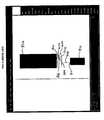
- FIG. 1 shows a simplified schematic block diagram of a[0004]
conventional FPGA 100 comprising a (2×2) array of programmable blocks. Each block inFPGA 100 comprises a programmable function unit (PFU)102 and a supplemental logic and interconnect cell (SLIC)104. Connected to these blocks are input/output (I/O) blocks. Each I/O block comprises four programmable I/O units (PIOs) connected to a programmable switch box. For example, fourPIOs 106 are connected to programmable switch box108, and fourPIOs 110 are connected toprogrammable switch box 112. In addition, FPGA100 is configured with horizontal and vertical wiring that provide routing resources for connecting the various functional elements (e.g., PIOs, PFUs, and SLICs) within the FPGA. For example, switch box108 is configured to be programmed to enablePIOs 106 to drive certain vertical wires114, whileswitch box 112 is configured to be programmed to enablePIOs 110 to drive certainhorizontal wires 116. In addition to switch boxes, such asswitch boxes 108 and112, which provide programmable interconnects between two different sets of wires,FPGA 100 also has programmable placedswitches 118, each of which enables a corresponding pair of intersecting horizontal and vertical wires to be connected (e.g., vertical wires114 andhorizontal PFU wires 120 orhorizontal wires 116 and vertical PFU wires122). FPGA100 will typically include much more routing resources to, from, and between the various functional elements than that shown in FIG. 1, as well as additional programmable switches and other logic components. - In general, an FPGA is a particular type of a programmable logic device (PLD) that can be programmed by the user for any of a wide range of specific applications. In theory, an FPGA, such as[0005]
FPGA 100 of FIG. 1, is provided with routing resources to connect (i.e., route) any pin on any component (e.g., a PFU, SLIC, or PIO) within the FPGA to any other pin on any other component within the FPGA. These connections are made by programming one or more programmable switches in the FPGA to establish a contiguous wiring path between the two pins. For example, in FIG. 1, PIO106-1 can be connected to pin2 of PFU102 by (i) programming switch box108 to connect PIO106-1 to vertical wire114 and (ii) programming placedswitch 118 to connect vertical wire114 tohorizontal wire 120, which is hard-wired to pin2 ofPFU 102. - Special software tools have been developed for programming FPGAs. One such programming tool is the Epic™ program provided to customers of FPGAs sold by Agere Systems Inc. of Berkeley Heights, N.J. Programming tools like the Epic™ program can be used by a programmer to generate graphical displays showing representations of the current programming of the FPGA. Although these graphical representations may conform generally to the actually physical design and layout of the physical FPGA chip, in fact, they are merely representations of the functionality provided by the FPGA. As such, the appearance of functional elements and routing resources in the graphical displays generated by the programming tool need not correspond identically to those in the actual FPGA device.[0006]
- In conventional software tools for programming FPGAs, different types of switches are typically supported. As described previously in the context of FIG. 1, an FPGA may have both programmable switch boxes, such as[0007]
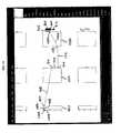
switch boxes 108 and112 as well as programmable placed switches, such as placedswitches 118. - FIG. 2 shows a schematic representation of a placed switch[0008]200, similar to placed
switch 118 of FIG. 1. Placed switch200 can be programmed to connecthorizontal wire 202 with “intersecting”vertical wire 204. When placed switch200 is on, it provides a connection betweenwires - FIG. 3 shows a schematic representation of a switch box[0009]300, similar to
switch boxes 108 and112 of FIG. 1. In theory, switch box300 can be implemented to programmably connect independently any ofinput wires 302 to any ofoutput wires 304. If the twoinput wires 302 are labeled A and B and the twooutput wires 304 are labeled C and D, switch box300 can be programmed in any of the sixteen different combinations of connections listed in Table I. In conventional programming tools for FPGAs, in order for an input wire to be connected to an output wire by a switch box, the two wires must be connected to the switch box in the graphical display of the FPGA generated by the programming tool.TABLE I Combination # Connections 1 None 2 A→C 3 A→D 4 B→C 5 B→D 6 A→C and B→D 7 A→D and B→C 8 A→C and A→D 9 B→C and B→D 10 A→C and B→C 11 A→D and B→D 12 A→C and A→D and B→C 13 A→C and A→D and B→D 14 A→C and B→C and B→D 15 A→D and B→C and B→D 16 A→C and A→D and B→C and B→D - FIG. 4 shows a schematic representation of a pseudo arc, another type of switch connection. A pseudo arc is the connection provided from an[0010]
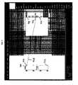
input wire 402 to anoutput wire 404 through a logic element400, such as a PFU or a SLIC. Typically, a pseudo arc is a conditional switch connection that depends on the logic implemented within element400. In conventional programming tools for FPGAs, in order for an input wire to be connected to an output wire via a pseudo are, the two wires must be connected to the same logic element in the graphical display of the FPGA generated by the programming tool. - FIG. 5 shows an example of a graphical display generated by the Epic™ program for a particular FPCA. FIG. 5 shows a display representing the entire FPGA in a single view. For a typical application, an FPGA such as that shown in FIG. 5 will be programmed with a large number of connections between the various functional elements. In order to be useful to programmers, the Epic™ program enables a programmer to generate displays that selectively reveal individual wiring routes between particular functional elements, including the programming of the individual switches that provide those routes. In addition, the Epic™ program can display all possible connections from a selected switch-box pin. The Epic™ program also enables a programmer to zoom in on any selected region of the display.[0011]
- FIG. 6 shows an example of a graphical display of one particular region of the FPGA shown in FIG. 5. In particular, FIG. 6 shows a[0012]
switch box 600 having a number ofinput pins 602 and a number ofoutput pins 604. In the display of FIG. 6, no connections are shown between any of the input and output pins. - FIG. 7 shows an example of a graphical display of[0013]
switch box 600 of FIG. 6 displaying all of the possible switch-box connections 702 involving aparticular input pin 602. As shown in FIG. 7,switch box 600 can be independently programmed to provide a different switch-box connection 702 frominput pin 602 to eachdifferent output pin 604. - FIG. 8 shows an example of a graphical display of an entire route from[0014]
output pin 804 of PFU802 to inputpin 810 of SLIC812. In particular, the entire route consists of (1)wire 806 connectingoutput pin 804 to inputpin 602 ofswitch box 600, (2) switch-box connection 702 connectinginput pin 602 tooutput pin 604 ofswitch box 600, and (3)wire 808 connectingoutput pin 604 toinput pin 810 of SLIC812. - In order for an FPGA to be programmed with a particular route, two requirements must be satisfied: (1) the set of actual connections that provide the particular route must be able to be made in the actual FPGA and (2) the set of actual connections that provide the particular route must be able to be represented in the graphical displays generated by the programming tool used to program the actual FPGA. Since the programming tool relies on a representation of the actual FPGA configuration, being able to satisfy the first requirement does not necessarily mean that the second requirement will also be able to be satisfied.[0015]
- In general, the types of connections (e.g., switch boxes, placed switches, and pseudo arcs) that are supported by conventional programming tools for FPGAs, such as the Epic™ program, have imposed constraints on the architectures of the actual FPGAs, because certain connections that could in theory be supported in actual FPGAs could not be represented using the types of connections supported by the conventional programming tools. For example, the types of connections supported by conventional programming tools require two wires to be co-located in the display generated by the programming tool in order for those wires to be connected. This means that the two wires have to either intersect one another or terminate at the same functional element. As a result, the number of different pins that could be designed into a particular functional element in the actual FPGA was limited by the number of corresponding wires connected to those pins that could be effectively represented in the graphical displays generated by the programming tool. As such, there was no point in designing FPGAs with functional elements having more than this number of pins, since such FPGAs could not be efficiently or reliably programmed using conventional programming tools. As such, FPGAs have not been designed with such architectures.[0016]
- The present invention is directed to a software tool for programming an FPGA that provides a novel technique for representing connections within an FPGA. In particular, in addition to all of the conventional placed switches, switch boxes, and pseudo arcs, embodiments of the present invention are able to represent FPGA connections using hidden switches. A hidden-switch connection is a connection between two functional elements that is represented in the graphical display generated by an FPGA programming software tool without explicitly representing the one or more switch devices that would provide the corresponding connection in the actual FPGA. In particular, a hidden-switch connection is represented in the graphical display as a curve (e.g., a diagonal straight line) from a jumper wire on one functional element to another jumper wire on another functional element, where a jumper wire is represented in the graphical display as a wire connected at one end to a pin of the corresponding functional element and unconnected at the other end.[0017]
- In one embodiment, the present invention is a method for representing programming for a programmable logic device (PLD), comprising the steps of (a) storing a software representation of the PLD; and (b) generating, based on the software representation of the PLD, a graphical display representing a hidden-switch connection between first and second functional elements in the PLD, wherein, in the graphical display, the hidden-switch connection is represented by a curve from a first jumper wire at a pin of the first functional element to a second jumper wire at a pin of the second functional element, wherein each jumper wire is represented as being connected to the corresponding pin of the corresponding functional element at a first end of the jumper wire and unconnected at a second end of the jumper wire.[0018]
- Other aspects, features, and advantages of the present invention will become more fully apparent from the following detailed description, the appended claims, and the accompanying drawings in which:[0019]
- FIG. 1 shows a simplified schematic block diagram of a conventional FPGA comprising a (2×2) array of programmable blocks;[0020]
- FIG. 2 shows a schematic representation of a placed switch;[0021]
- FIG. 3 shows a schematic representation of a switch box;[0022]
- FIG. 4 shows a schematic representation of a pseudo arc;[0023]
- FIG. 5 shows an example of a graphical display generated by the Epic™ program for a particular FPGA;[0024]
- FIG. 6 shows an example of a graphical display of one particular region of the FPGA shown in FIG. 5;[0025]
- FIG. 7 shows an example of a graphical display of the switch box of FIG. 6;[0026]
- FIG. 8 shows an example of a graphical display of an entire route;[0027]
- FIG. 9 shows an example of a graphical display of a hidden-switch connection generated by a programming tool for FPGAs, according to one embodiment of the present invention; and[0028]
- FIG. 10 shows an example of a graphical display generated by a programming tool of the present invention representing two routes.[0029]
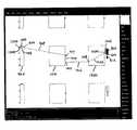
- FIG. 9 shows an example of a graphical display of a hidden-switch connection generated by a programming tool for FPGAs, according to one embodiment of the present invention. In particular, the display of FIG. 9 represents a hidden-switch connection between[0030]
pin 904 ofswitch box 902 and pin912 ofswitch box 914. As shown in FIG. 9, the hidden-switch connection is represented by (1)jumper wire 906 connected to pin904 ofswitch box 902, (2)jumper wire 910 connected to pin912 ofswitch box 914, anddiagonal line 908 connectingjumper wire 906 tojumper wire 910. Note that FIG. 9 shows many other jumper wires, such asjumper wires - Conventional connections, such as placed-switch, switch-box, and pseudo-arc connections, are all based on explicit representations of physical switch devices in the actual FPGA that provide the connections (i.e., placed switches, switch boxes, and logic elements). Moreover, the input and output wires for such conventional connections must be co-located in the displays generated by the programming tool (e.g., intersecting in the case of placed-switch connections and terminating at the same functional element in the case of switch-box and pseudo-arc connections). A hidden-switch connection does not share those characteristics. In particular, a hidden-switch connection is represented in the graphical displays generated by the programming tool of the present invention without explicitly representing the physical switch devices that provide the physical connection in the actual FPGA. In that sense, those corresponding physical switch devices may be said to be hidden. Furthermore, the two wires involved in a hidden-switch connection are represented by a pair of jumper wires that do not have to be co-located in the displays generated by the programming tools.[0031]
- FIG. 10 shows an example of a graphical display generated by a programming tool of the present invention representing two routes through numerous functional elements (i.e., switch[0032]
boxes PIO 1002 toPFU 802 and a second route from PFU,802 toSLIC 812. In particular, the first route of FIG. 10 includes: - [0033]
Conventional wire 1004 connectingPIO 1002 to inputpin 1006 ofswitch box 902; - Conventional switch-[0034]
box connection 1008 connectinginput pin 1006 ofswitch box 902 tooutput pin 904 ofswitch box 902; - The hidden-switch connection of FIG. 9 consisting of[0035]
diagonal line 908 connectingjumper wire 906 atoutput pin 904 ofswitch box 902 tojumper wire 910 atinput pin 912 ofswitch box 914; - A conventional switch-box connection connecting[0036]
input pin 912 ofswitch box 914 to an output pin ofswitch box 914; - A conventional wire connecting that output pin of[0037]
switch box 914 to an input pin ofswitch box 1010; - Conventional switch-[0038]
box connection 1012 connecting that input pin ofswitch box 1010 tooutput pin 1014 ofswitch box 1010; - [0039]
Conventional wire 1016 connectingoutput pin 1014 ofswitch box 1010 to inputpin 1018 ofswitch box 1020; - Conventional switch-[0040]
box connection 1022 connectinginput pin 1018 ofswitch box 1020 tooutput pin 1024 ofswitch box 1020; and - [0041]
Conventional wire 1026 connectingoutput pin 1024 ofswitch box 1020 to an input pin ofPFU 802. - The second route of FIG. 10 includes:[0042]
- [0043]
Conventional wire 806 connectingoutput pin 804 ofPFU 802 to inputpin 602 of switch box600 (as shown more clearly in FIG. 8); - Conventional switch-[0044]
box connection 702 connectinginput pin 602 ofswitch box 600 tooutput pin 604 of switch box600 (as shown more clearly in FIG. 8); and - [0045]
Conventional wire 808 connectingoutput pin 604 ofswitch box 600 to inputpin 810 of SLIC812 (as shown more clearly in FIG. 8). - A programming tool for FPGAs that supports hidden-switch connections, in addition to conventional placed-switch, switch-box, and pseudo-arc connections, allows a wider variety of architectures for the FPGA being programmed. In particular, since connections can be represented as being provided by hidden switches, the number of pins that can be designed into a particular functional element is no longer limited to the number of wires connected to that functional element that can be efficiently represented in the graphical display generated by the programming tool. In particular, the process of generating the software model of a particular FPGA hardware design for use in the programming tool is much easier with the addition of hidden-switch connections. As such, FPGAs having functional elements with greater numbers of pins are much more easily realizable with the present invention than with the prior-art programming tools.[0046]
- Although the present invention has been described in the context of FPGAs, those skilled in the art will understand that the present invention can be implemented in the context of other types of programmable logic devices, such as a field programmable system on a chip (FPSC) or an embedded FPGA (EFPGA), which is an array of programmable logic embedded within an application specific integrated circuit (ASIC).[0047]
- The present invention may be implemented as circuit-based processes, including possible implementation on a single integrated circuit. As would be apparent to one skilled in the art, various functions of circuit elements may also be implemented as processing steps in a software program. Such software may be employed in, for example, a digital signal processor, micro-controller, or general-purpose computer.[0048]
- The present invention can be embodied in the form of methods and apparatuses for practicing those methods. The present invention can also be embodied in the form of program code embodied in tangible media, such as floppy diskettes, CD-ROMs, hard drives, or any other machine-readable storage medium, wherein, when the program code is loaded into and executed by a machine, such as a computer, the machine becomes an apparatus for practicing the invention. The present invention can also be embodied in the form of program code, for example, whether stored in a storage medium, loaded into and/or executed by a machine, or transmitted over some transmission medium or carrier, such as over electrical wiring or cabling, through fiber optics, or via electromagnetic radiation, wherein, when the program code is loaded into and executed by a machine, such as a computer, the machine becomes an apparatus for practicing the invention. When implemented on a general-purpose processor, the program code segments combine with the processor to provide a unique device that operates analogously to specific logic circuits.[0049]
- It will be further understood that various changes in the details, materials, and arrangements of the parts which have been described and illustrated in order to explain the nature of this invention may be made by those skilled in the art without departing from the scope of the invention as expressed in the following claims.[0050]
Claims (16)
Priority Applications (2)
| Application Number | Priority Date | Filing Date | Title |
|---|---|---|---|
| US09/818,257US6496969B2 (en) | 2001-03-27 | 2001-03-27 | Programming programmable logic devices using hidden switches |
| US10/263,251US6748575B1 (en) | 2001-03-27 | 2002-10-02 | Programming programmable logic devices using hidden switches |
Applications Claiming Priority (1)
| Application Number | Priority Date | Filing Date | Title |
|---|---|---|---|
| US09/818,257US6496969B2 (en) | 2001-03-27 | 2001-03-27 | Programming programmable logic devices using hidden switches |
Related Child Applications (1)
| Application Number | Title | Priority Date | Filing Date |
|---|---|---|---|
| US10/263,251ContinuationUS6748575B1 (en) | 2001-03-27 | 2002-10-02 | Programming programmable logic devices using hidden switches |
Publications (2)
| Publication Number | Publication Date |
|---|---|
| US20020174411A1true US20020174411A1 (en) | 2002-11-21 |
| US6496969B2 US6496969B2 (en) | 2002-12-17 |
Family
ID=25225075
Family Applications (2)
| Application Number | Title | Priority Date | Filing Date |
|---|---|---|---|
| US09/818,257Expired - LifetimeUS6496969B2 (en) | 2001-03-27 | 2001-03-27 | Programming programmable logic devices using hidden switches |
| US10/263,251Expired - LifetimeUS6748575B1 (en) | 2001-03-27 | 2002-10-02 | Programming programmable logic devices using hidden switches |
Family Applications After (1)
| Application Number | Title | Priority Date | Filing Date |
|---|---|---|---|
| US10/263,251Expired - LifetimeUS6748575B1 (en) | 2001-03-27 | 2002-10-02 | Programming programmable logic devices using hidden switches |
Country Status (1)
| Country | Link |
|---|---|
| US (2) | US6496969B2 (en) |
Cited By (40)
| Publication number | Priority date | Publication date | Assignee | Title |
|---|---|---|---|---|
| US20050097305A1 (en)* | 2003-10-30 | 2005-05-05 | International Business Machines Corporation | Method and apparatus for using FPGA technology with a microprocessor for reconfigurable, instruction level hardware acceleration |
| US7737724B2 (en) | 2007-04-17 | 2010-06-15 | Cypress Semiconductor Corporation | Universal digital block interconnection and channel routing |
| US7761845B1 (en) | 2002-09-09 | 2010-07-20 | Cypress Semiconductor Corporation | Method for parameterizing a user module |
| US7765095B1 (en) | 2000-10-26 | 2010-07-27 | Cypress Semiconductor Corporation | Conditional branching in an in-circuit emulation system |
| US7770113B1 (en) | 2001-11-19 | 2010-08-03 | Cypress Semiconductor Corporation | System and method for dynamically generating a configuration datasheet |
| US7774190B1 (en) | 2001-11-19 | 2010-08-10 | Cypress Semiconductor Corporation | Sleep and stall in an in-circuit emulation system |
| US7825688B1 (en) | 2000-10-26 | 2010-11-02 | Cypress Semiconductor Corporation | Programmable microcontroller architecture(mixed analog/digital) |
| US7844437B1 (en) | 2001-11-19 | 2010-11-30 | Cypress Semiconductor Corporation | System and method for performing next placements and pruning of disallowed placements for programming an integrated circuit |
| US7893724B2 (en) | 2004-03-25 | 2011-02-22 | Cypress Semiconductor Corporation | Method and circuit for rapid alignment of signals |
| US8026739B2 (en) | 2007-04-17 | 2011-09-27 | Cypress Semiconductor Corporation | System level interconnect with programmable switching |
| US8040266B2 (en) | 2007-04-17 | 2011-10-18 | Cypress Semiconductor Corporation | Programmable sigma-delta analog-to-digital converter |
| US8049569B1 (en) | 2007-09-05 | 2011-11-01 | Cypress Semiconductor Corporation | Circuit and method for improving the accuracy of a crystal-less oscillator having dual-frequency modes |
| US8069428B1 (en) | 2001-10-24 | 2011-11-29 | Cypress Semiconductor Corporation | Techniques for generating microcontroller configuration information |
| US8067948B2 (en) | 2006-03-27 | 2011-11-29 | Cypress Semiconductor Corporation | Input/output multiplexer bus |
| US8069405B1 (en) | 2001-11-19 | 2011-11-29 | Cypress Semiconductor Corporation | User interface for efficiently browsing an electronic document using data-driven tabs |
| US8069436B2 (en) | 2004-08-13 | 2011-11-29 | Cypress Semiconductor Corporation | Providing hardware independence to automate code generation of processing device firmware |
| US8078894B1 (en) | 2007-04-25 | 2011-12-13 | Cypress Semiconductor Corporation | Power management architecture, method and configuration system |
| US8078970B1 (en) | 2001-11-09 | 2011-12-13 | Cypress Semiconductor Corporation | Graphical user interface with user-selectable list-box |
| US8085100B2 (en) | 2005-02-04 | 2011-12-27 | Cypress Semiconductor Corporation | Poly-phase frequency synthesis oscillator |
| US8085067B1 (en) | 2005-12-21 | 2011-12-27 | Cypress Semiconductor Corporation | Differential-to-single ended signal converter circuit and method |
| US8089461B2 (en) | 2005-06-23 | 2012-01-03 | Cypress Semiconductor Corporation | Touch wake for electronic devices |
| US8092083B2 (en) | 2007-04-17 | 2012-01-10 | Cypress Semiconductor Corporation | Temperature sensor with digital bandgap |
| US8103497B1 (en) | 2002-03-28 | 2012-01-24 | Cypress Semiconductor Corporation | External interface for event architecture |
| US8103496B1 (en) | 2000-10-26 | 2012-01-24 | Cypress Semicondutor Corporation | Breakpoint control in an in-circuit emulation system |
| US8120408B1 (en) | 2005-05-05 | 2012-02-21 | Cypress Semiconductor Corporation | Voltage controlled oscillator delay cell and method |
| US8130025B2 (en) | 2007-04-17 | 2012-03-06 | Cypress Semiconductor Corporation | Numerical band gap |
| US8149048B1 (en) | 2000-10-26 | 2012-04-03 | Cypress Semiconductor Corporation | Apparatus and method for programmable power management in a programmable analog circuit block |
| US8160864B1 (en) | 2000-10-26 | 2012-04-17 | Cypress Semiconductor Corporation | In-circuit emulator and pod synchronized boot |
| US8176296B2 (en) | 2000-10-26 | 2012-05-08 | Cypress Semiconductor Corporation | Programmable microcontroller architecture |
| US8286125B2 (en) | 2004-08-13 | 2012-10-09 | Cypress Semiconductor Corporation | Model for a hardware device-independent method of defining embedded firmware for programmable systems |
| US8402313B1 (en) | 2002-05-01 | 2013-03-19 | Cypress Semiconductor Corporation | Reconfigurable testing system and method |
| US8499270B1 (en) | 2007-04-25 | 2013-07-30 | Cypress Semiconductor Corporation | Configuration of programmable IC design elements |
| US8516025B2 (en) | 2007-04-17 | 2013-08-20 | Cypress Semiconductor Corporation | Clock driven dynamic datapath chaining |
| US8533677B1 (en) | 2001-11-19 | 2013-09-10 | Cypress Semiconductor Corporation | Graphical user interface for dynamically reconfiguring a programmable device |
| CN103699046A (en)* | 2013-11-14 | 2014-04-02 | 南京航空航天大学 | Universal wiring switch box for island type FPGA (Field Programmable Gate Array) |
| US9448964B2 (en) | 2009-05-04 | 2016-09-20 | Cypress Semiconductor Corporation | Autonomous control in a programmable system |
| US9564902B2 (en) | 2007-04-17 | 2017-02-07 | Cypress Semiconductor Corporation | Dynamically configurable and re-configurable data path |
| US9720805B1 (en) | 2007-04-25 | 2017-08-01 | Cypress Semiconductor Corporation | System and method for controlling a target device |
| US20170250690A1 (en)* | 2014-08-20 | 2017-08-31 | Areva Np Sas | Circuit arrangement for a safety i&c system |
| US10698662B2 (en) | 2001-11-15 | 2020-06-30 | Cypress Semiconductor Corporation | System providing automatic source code generation for personalization and parameterization of user modules |
Families Citing this family (8)
| Publication number | Priority date | Publication date | Assignee | Title |
|---|---|---|---|---|
| US6300794B1 (en)* | 1996-10-10 | 2001-10-09 | Altera Corporation | Programmable logic device with hierarchical interconnection resources |
| US7155711B2 (en)* | 1999-12-10 | 2006-12-26 | Sedna Patent Services, Llc | Method and apparatus providing remote reprogramming of programmable logic devices using embedded JTAG physical layer and protocol |
| US20030004672A1 (en)* | 2001-06-29 | 2003-01-02 | National Instruments Corporation | Meta-routing tool for a measurement system |
| US7100139B1 (en)* | 2002-04-08 | 2006-08-29 | Cypress Semiconductor Corporation | Pinout views for allowed connections in GUI |
| US6915212B2 (en)* | 2003-05-08 | 2005-07-05 | Moac, Llc | Systems and methods for processing complex data sets |
| US6996470B2 (en)* | 2003-08-01 | 2006-02-07 | Moac Llc | Systems and methods for geophysical imaging using amorphous computational processing |
| CN108427829B (en)* | 2018-02-09 | 2022-11-08 | 京微齐力(北京)科技有限公司 | FPGA with common line structure |
| CN108920398B (en) | 2018-07-05 | 2021-01-19 | 苏州浪潮智能科技有限公司 | Cap jump circuit and design method thereof |
Family Cites Families (6)
| Publication number | Priority date | Publication date | Assignee | Title |
|---|---|---|---|---|
| US4870302A (en) | 1984-03-12 | 1989-09-26 | Xilinx, Inc. | Configurable electrical circuit having configurable logic elements and configurable interconnects |
| US4845633A (en)* | 1985-12-02 | 1989-07-04 | Apple Computer Inc. | System for programming graphically a programmable, asynchronous logic cell and array |
| US5367208A (en)* | 1986-09-19 | 1994-11-22 | Actel Corporation | Reconfigurable programmable interconnect architecture |
| US5448493A (en) | 1989-12-20 | 1995-09-05 | Xilinx, Inc. | Structure and method for manually controlling automatic configuration in an integrated circuit logic block array |
| US5649163A (en)* | 1992-10-29 | 1997-07-15 | Altera Corporation | Method of programming an asynchronous load storage device using a representation of a clear/preset storage device |
| US6294928B1 (en)* | 1996-04-05 | 2001-09-25 | Altera Corporation | Programmable logic device with highly routable interconnect |
- 2001
- 2001-03-27USUS09/818,257patent/US6496969B2/ennot_activeExpired - Lifetime
- 2002
- 2002-10-02USUS10/263,251patent/US6748575B1/ennot_activeExpired - Lifetime
Cited By (59)
| Publication number | Priority date | Publication date | Assignee | Title |
|---|---|---|---|---|
| US9843327B1 (en) | 2000-10-26 | 2017-12-12 | Cypress Semiconductor Corporation | PSOC architecture |
| US8358150B1 (en) | 2000-10-26 | 2013-01-22 | Cypress Semiconductor Corporation | Programmable microcontroller architecture(mixed analog/digital) |
| US8555032B2 (en) | 2000-10-26 | 2013-10-08 | Cypress Semiconductor Corporation | Microcontroller programmable system on a chip with programmable interconnect |
| US10725954B2 (en) | 2000-10-26 | 2020-07-28 | Monterey Research, Llc | Microcontroller programmable system on a chip |
| US8736303B2 (en) | 2000-10-26 | 2014-05-27 | Cypress Semiconductor Corporation | PSOC architecture |
| US7765095B1 (en) | 2000-10-26 | 2010-07-27 | Cypress Semiconductor Corporation | Conditional branching in an in-circuit emulation system |
| US10248604B2 (en) | 2000-10-26 | 2019-04-02 | Cypress Semiconductor Corporation | Microcontroller programmable system on a chip |
| US9766650B2 (en) | 2000-10-26 | 2017-09-19 | Cypress Semiconductor Corporation | Microcontroller programmable system on a chip with programmable interconnect |
| US7825688B1 (en) | 2000-10-26 | 2010-11-02 | Cypress Semiconductor Corporation | Programmable microcontroller architecture(mixed analog/digital) |
| US10020810B2 (en) | 2000-10-26 | 2018-07-10 | Cypress Semiconductor Corporation | PSoC architecture |
| US8176296B2 (en) | 2000-10-26 | 2012-05-08 | Cypress Semiconductor Corporation | Programmable microcontroller architecture |
| US8103496B1 (en) | 2000-10-26 | 2012-01-24 | Cypress Semicondutor Corporation | Breakpoint control in an in-circuit emulation system |
| US8149048B1 (en) | 2000-10-26 | 2012-04-03 | Cypress Semiconductor Corporation | Apparatus and method for programmable power management in a programmable analog circuit block |
| US10261932B2 (en) | 2000-10-26 | 2019-04-16 | Cypress Semiconductor Corporation | Microcontroller programmable system on a chip |
| US8160864B1 (en) | 2000-10-26 | 2012-04-17 | Cypress Semiconductor Corporation | In-circuit emulator and pod synchronized boot |
| US8069428B1 (en) | 2001-10-24 | 2011-11-29 | Cypress Semiconductor Corporation | Techniques for generating microcontroller configuration information |
| US10466980B2 (en) | 2001-10-24 | 2019-11-05 | Cypress Semiconductor Corporation | Techniques for generating microcontroller configuration information |
| US8793635B1 (en) | 2001-10-24 | 2014-07-29 | Cypress Semiconductor Corporation | Techniques for generating microcontroller configuration information |
| US8078970B1 (en) | 2001-11-09 | 2011-12-13 | Cypress Semiconductor Corporation | Graphical user interface with user-selectable list-box |
| US10698662B2 (en) | 2001-11-15 | 2020-06-30 | Cypress Semiconductor Corporation | System providing automatic source code generation for personalization and parameterization of user modules |
| US8069405B1 (en) | 2001-11-19 | 2011-11-29 | Cypress Semiconductor Corporation | User interface for efficiently browsing an electronic document using data-driven tabs |
| US7844437B1 (en) | 2001-11-19 | 2010-11-30 | Cypress Semiconductor Corporation | System and method for performing next placements and pruning of disallowed placements for programming an integrated circuit |
| US7770113B1 (en) | 2001-11-19 | 2010-08-03 | Cypress Semiconductor Corporation | System and method for dynamically generating a configuration datasheet |
| US7774190B1 (en) | 2001-11-19 | 2010-08-10 | Cypress Semiconductor Corporation | Sleep and stall in an in-circuit emulation system |
| US8533677B1 (en) | 2001-11-19 | 2013-09-10 | Cypress Semiconductor Corporation | Graphical user interface for dynamically reconfiguring a programmable device |
| US8370791B2 (en) | 2001-11-19 | 2013-02-05 | Cypress Semiconductor Corporation | System and method for performing next placements and pruning of disallowed placements for programming an integrated circuit |
| US8103497B1 (en) | 2002-03-28 | 2012-01-24 | Cypress Semiconductor Corporation | External interface for event architecture |
| US8402313B1 (en) | 2002-05-01 | 2013-03-19 | Cypress Semiconductor Corporation | Reconfigurable testing system and method |
| US7761845B1 (en) | 2002-09-09 | 2010-07-20 | Cypress Semiconductor Corporation | Method for parameterizing a user module |
| US7584345B2 (en) | 2003-10-30 | 2009-09-01 | International Business Machines Corporation | System for using FPGA technology with a microprocessor for reconfigurable, instruction level hardware acceleration |
| US20050097305A1 (en)* | 2003-10-30 | 2005-05-05 | International Business Machines Corporation | Method and apparatus for using FPGA technology with a microprocessor for reconfigurable, instruction level hardware acceleration |
| US7603540B2 (en) | 2003-10-30 | 2009-10-13 | International Business Machines Corporation | Using field programmable gate array (FPGA) technology with a microprocessor for reconfigurable, instruction level hardware acceleration |
| US7893724B2 (en) | 2004-03-25 | 2011-02-22 | Cypress Semiconductor Corporation | Method and circuit for rapid alignment of signals |
| US8286125B2 (en) | 2004-08-13 | 2012-10-09 | Cypress Semiconductor Corporation | Model for a hardware device-independent method of defining embedded firmware for programmable systems |
| US8069436B2 (en) | 2004-08-13 | 2011-11-29 | Cypress Semiconductor Corporation | Providing hardware independence to automate code generation of processing device firmware |
| US8085100B2 (en) | 2005-02-04 | 2011-12-27 | Cypress Semiconductor Corporation | Poly-phase frequency synthesis oscillator |
| US8120408B1 (en) | 2005-05-05 | 2012-02-21 | Cypress Semiconductor Corporation | Voltage controlled oscillator delay cell and method |
| US8089461B2 (en) | 2005-06-23 | 2012-01-03 | Cypress Semiconductor Corporation | Touch wake for electronic devices |
| US8085067B1 (en) | 2005-12-21 | 2011-12-27 | Cypress Semiconductor Corporation | Differential-to-single ended signal converter circuit and method |
| US8067948B2 (en) | 2006-03-27 | 2011-11-29 | Cypress Semiconductor Corporation | Input/output multiplexer bus |
| US8717042B1 (en) | 2006-03-27 | 2014-05-06 | Cypress Semiconductor Corporation | Input/output multiplexer bus |
| US8092083B2 (en) | 2007-04-17 | 2012-01-10 | Cypress Semiconductor Corporation | Temperature sensor with digital bandgap |
| US8040266B2 (en) | 2007-04-17 | 2011-10-18 | Cypress Semiconductor Corporation | Programmable sigma-delta analog-to-digital converter |
| US8482313B2 (en) | 2007-04-17 | 2013-07-09 | Cypress Semiconductor Corporation | Universal digital block interconnection and channel routing |
| US7737724B2 (en) | 2007-04-17 | 2010-06-15 | Cypress Semiconductor Corporation | Universal digital block interconnection and channel routing |
| US9564902B2 (en) | 2007-04-17 | 2017-02-07 | Cypress Semiconductor Corporation | Dynamically configurable and re-configurable data path |
| US8026739B2 (en) | 2007-04-17 | 2011-09-27 | Cypress Semiconductor Corporation | System level interconnect with programmable switching |
| US8130025B2 (en) | 2007-04-17 | 2012-03-06 | Cypress Semiconductor Corporation | Numerical band gap |
| US8476928B1 (en) | 2007-04-17 | 2013-07-02 | Cypress Semiconductor Corporation | System level interconnect with programmable switching |
| US8516025B2 (en) | 2007-04-17 | 2013-08-20 | Cypress Semiconductor Corporation | Clock driven dynamic datapath chaining |
| US8499270B1 (en) | 2007-04-25 | 2013-07-30 | Cypress Semiconductor Corporation | Configuration of programmable IC design elements |
| US8909960B1 (en) | 2007-04-25 | 2014-12-09 | Cypress Semiconductor Corporation | Power management architecture, method and configuration system |
| US9720805B1 (en) | 2007-04-25 | 2017-08-01 | Cypress Semiconductor Corporation | System and method for controlling a target device |
| US8078894B1 (en) | 2007-04-25 | 2011-12-13 | Cypress Semiconductor Corporation | Power management architecture, method and configuration system |
| US8049569B1 (en) | 2007-09-05 | 2011-11-01 | Cypress Semiconductor Corporation | Circuit and method for improving the accuracy of a crystal-less oscillator having dual-frequency modes |
| US9448964B2 (en) | 2009-05-04 | 2016-09-20 | Cypress Semiconductor Corporation | Autonomous control in a programmable system |
| CN103699046A (en)* | 2013-11-14 | 2014-04-02 | 南京航空航天大学 | Universal wiring switch box for island type FPGA (Field Programmable Gate Array) |
| US20170250690A1 (en)* | 2014-08-20 | 2017-08-31 | Areva Np Sas | Circuit arrangement for a safety i&c system |
| US10547313B2 (en)* | 2014-08-20 | 2020-01-28 | Areva Np Sas | Circuit arrangement for a safety IandC system |
Also Published As
| Publication number | Publication date |
|---|---|
| US6496969B2 (en) | 2002-12-17 |
| US6748575B1 (en) | 2004-06-08 |
Similar Documents
| Publication | Publication Date | Title |
|---|---|---|
| US6496969B2 (en) | Programming programmable logic devices using hidden switches | |
| US5761099A (en) | Programmable logic array integrated circuits with enhanced carry routing | |
| US6690195B1 (en) | Driver circuitry for programmable logic devices | |
| US5396126A (en) | FPGA with distributed switch matrix | |
| US6747480B1 (en) | Programmable logic devices with bidirect ional cascades | |
| US5367209A (en) | Field programmable gate array for synchronous and asynchronous operation | |
| US7953956B2 (en) | Reconfigurable circuit with a limitation on connection and method of determining functions of logic circuits in the reconfigurable circuit | |
| US8093922B2 (en) | Configurable IC having a routing fabric with storage elements | |
| US5796267A (en) | Tri-Statable input/output circuitry for programmable logic | |
| US6181162B1 (en) | Programmable logic device with highly routable interconnect | |
| EP0746102B1 (en) | Programmable logic array integrated circuit | |
| US20130135009A1 (en) | Method and apparatus for identifying connections between configurable nodes in a configurable integrated circuit | |
| US20070241786A1 (en) | Configurable Integrated Circuit with Different Connection Schemes | |
| US7605605B2 (en) | Programmable logic cells with local connections | |
| US20120062278A1 (en) | Configurable integrated circuit with built-in turns | |
| US7165230B2 (en) | Switch methodology for mask-programmable logic devices | |
| JPH0282814A (en) | Programmable logic device | |
| US20140210513A1 (en) | Controllable Storage Elements for an IC | |
| US8390321B2 (en) | Reconfigurable logical circuit | |
| KR930001749B1 (en) | Programmable logic circuit | |
| KR20050065621A (en) | Spare cell architecture for fixing design errors in manufactured integrated circuits | |
| US6260175B1 (en) | Method for designing an integrated circuit using predefined and preverified core modules having prebalanced clock trees | |
| US6353352B1 (en) | Clock tree topology | |
| JPH0258810B2 (en) | ||
| US6983442B1 (en) | Method for constructing an integrated circuit device having fixed and programmable logic portions and programmable logic architecture for use therewith |
Legal Events
| Date | Code | Title | Description |
|---|---|---|---|
| AS | Assignment | Owner name:AGERE SYSTEMS GUARDIAN CORP., FLORIDA Free format text:ASSIGNMENT OF ASSIGNORS INTEREST;ASSIGNORS:FENG, WENYI;TING, ERIC;OSWALD, WILLIAM A.;AND OTHERS;REEL/FRAME:011882/0149;SIGNING DATES FROM 20010319 TO 20010328 | |
| FEPP | Fee payment procedure | Free format text:PAYOR NUMBER ASSIGNED (ORIGINAL EVENT CODE: ASPN); ENTITY STATUS OF PATENT OWNER: LARGE ENTITY | |
| AS | Assignment | Owner name:AGERE SYSTEMS GUARDIAN CORP., FLORIDA Free format text:ASSIGNMENT OF ASSIGNORS INTEREST;ASSIGNOR:LUCENT TECHNOLOGIES INC.;REEL/FRAME:012510/0274 Effective date:20010131 | |
| AS | Assignment | Owner name:LATTICE SEMICONDUCTOR CORPORATION, OREGON Free format text:ASSIGNMENT OF ASSIGNORS INTEREST;ASSIGNOR:AGERE SYSTEMS GUARDIAN CORPORATION;REEL/FRAME:012631/0900 Effective date:20020115 | |
| STCF | Information on status: patent grant | Free format text:PATENTED CASE | |
| FPAY | Fee payment | Year of fee payment:4 | |
| FPAY | Fee payment | Year of fee payment:8 | |
| FPAY | Fee payment | Year of fee payment:12 | |
| AS | Assignment | Owner name:JEFFERIES FINANCE LLC, NEW YORK Free format text:SECURITY INTEREST;ASSIGNORS:LATTICE SEMICONDUCTOR CORPORATION;SIBEAM, INC.;SILICON IMAGE, INC.;AND OTHERS;REEL/FRAME:035225/0839 Effective date:20150310 | |
| AS | Assignment | Owner name:LATTICE SEMICONDUCTOR CORPORATION, OREGON Free format text:RELEASE BY SECURED PARTY;ASSIGNOR:JEFFERIES FINANCE LLC;REEL/FRAME:049827/0326 Effective date:20190517 Owner name:DVDO, INC., OREGON Free format text:RELEASE BY SECURED PARTY;ASSIGNOR:JEFFERIES FINANCE LLC;REEL/FRAME:049827/0326 Effective date:20190517 Owner name:SIBEAM, INC., OREGON Free format text:RELEASE BY SECURED PARTY;ASSIGNOR:JEFFERIES FINANCE LLC;REEL/FRAME:049827/0326 Effective date:20190517 Owner name:SILICON IMAGE, INC., OREGON Free format text:RELEASE BY SECURED PARTY;ASSIGNOR:JEFFERIES FINANCE LLC;REEL/FRAME:049827/0326 Effective date:20190517 Owner name:WELLS FARGO BANK, NATIONAL ASSOCIATION, AS ADMINIS Free format text:SECURITY INTEREST;ASSIGNOR:LATTICE SEMICONDUCTOR CORPORATION;REEL/FRAME:049980/0786 Effective date:20190517 Owner name:WELLS FARGO BANK, NATIONAL ASSOCIATION, AS ADMINISTRATIVE AGENT, COLORADO Free format text:SECURITY INTEREST;ASSIGNOR:LATTICE SEMICONDUCTOR CORPORATION;REEL/FRAME:049980/0786 Effective date:20190517 |