US20020173083A1 - Methodology for electrically induced selective breakdown of nanotubes - Google Patents
Methodology for electrically induced selective breakdown of nanotubesDownload PDFInfo
- Publication number
- US20020173083A1 US20020173083A1US10/144,402US14440202AUS2002173083A1US 20020173083 A1US20020173083 A1US 20020173083A1US 14440202 AUS14440202 AUS 14440202AUS 2002173083 A1US2002173083 A1US 2002173083A1
- Authority
- US
- United States
- Prior art keywords
- nanotubes
- substrate
- nanotube
- field effect
- effect transistor
- Prior art date
- Legal status (The legal status is an assumption and is not a legal conclusion. Google has not performed a legal analysis and makes no representation as to the accuracy of the status listed.)
- Granted
Links
- 239000002071nanotubeSubstances0.000titleclaimsabstractdescription134
- 238000000034methodMethods0.000titleclaimsabstractdescription78
- 230000015556catabolic processEffects0.000titledescription32
- 239000000758substrateSubstances0.000claimsabstractdescription50
- 239000002184metalSubstances0.000claimsabstractdescription43
- 229910052751metalInorganic materials0.000claimsabstractdescription43
- 238000000151depositionMethods0.000claimsabstractdescription25
- 238000004140cleaningMethods0.000claimsabstractdescription8
- 239000002109single walled nanotubeSubstances0.000claimsdescription78
- 239000002048multi walled nanotubeSubstances0.000claimsdescription53
- OKTJSMMVPCPJKN-UHFFFAOYSA-NCarbonChemical compound[C]OKTJSMMVPCPJKN-UHFFFAOYSA-N0.000claimsdescription49
- 230000005669field effectEffects0.000claimsdescription32
- 239000002041carbon nanotubeSubstances0.000claimsdescription31
- 229910021393carbon nanotubeInorganic materials0.000claimsdescription31
- 239000000969carrierSubstances0.000claimsdescription16
- 239000007789gasSubstances0.000claimsdescription12
- VYPSYNLAJGMNEJ-UHFFFAOYSA-NSilicium dioxideChemical groupO=[Si]=OVYPSYNLAJGMNEJ-UHFFFAOYSA-N0.000claimsdescription8
- 238000000137annealingMethods0.000claimsdescription8
- 230000000779depleting effectEffects0.000claimsdescription7
- 238000001459lithographyMethods0.000claimsdescription7
- 239000012212insulatorSubstances0.000claimsdescription4
- 239000000377silicon dioxideSubstances0.000claimsdescription4
- 239000011261inert gasSubstances0.000claimsdescription3
- 229910052799carbonInorganic materials0.000description17
- 239000004020conductorSubstances0.000description7
- 238000010586diagramMethods0.000description7
- 238000005259measurementMethods0.000description7
- 239000000203mixtureSubstances0.000description7
- 239000004065semiconductorSubstances0.000description7
- 230000004888barrier functionEffects0.000description6
- 230000007423decreaseEffects0.000description6
- 230000032258transportEffects0.000description6
- 230000006399behaviorEffects0.000description5
- 230000015572biosynthetic processEffects0.000description5
- 239000002131composite materialSubstances0.000description5
- 239000010410layerSubstances0.000description5
- 230000003647oxidationEffects0.000description5
- 238000007254oxidation reactionMethods0.000description5
- 230000008569processEffects0.000description5
- 239000000523sampleSubstances0.000description5
- 238000006243chemical reactionMethods0.000description4
- 239000000470constituentSubstances0.000description4
- 230000006378damageEffects0.000description4
- 230000003993interactionEffects0.000description4
- 230000035882stressEffects0.000description4
- PZNSFCLAULLKQX-UHFFFAOYSA-NBoron nitrideChemical compoundN#BPZNSFCLAULLKQX-UHFFFAOYSA-N0.000description3
- QVGXLLKOCUKJST-UHFFFAOYSA-Natomic oxygenChemical compound[O]QVGXLLKOCUKJST-UHFFFAOYSA-N0.000description3
- 230000008859changeEffects0.000description3
- 238000012512characterization methodMethods0.000description3
- 238000009826distributionMethods0.000description3
- 238000002474experimental methodMethods0.000description3
- 239000000463materialSubstances0.000description3
- 230000004048modificationEffects0.000description3
- 238000012986modificationMethods0.000description3
- 239000002086nanomaterialSubstances0.000description3
- 239000001301oxygenSubstances0.000description3
- 229910052760oxygenInorganic materials0.000description3
- 230000035945sensitivityEffects0.000description3
- 238000000926separation methodMethods0.000description3
- 239000000126substanceSubstances0.000description3
- 238000003786synthesis reactionMethods0.000description3
- 230000008878couplingEffects0.000description2
- 238000010168coupling processMethods0.000description2
- 238000005859coupling reactionMethods0.000description2
- 230000007547defectEffects0.000description2
- 230000001419dependent effectEffects0.000description2
- 230000008021depositionEffects0.000description2
- 238000013461designMethods0.000description2
- 230000001747exhibiting effectEffects0.000description2
- 230000006870functionEffects0.000description2
- 229910002804graphiteInorganic materials0.000description2
- 239000010439graphiteSubstances0.000description2
- 230000000977initiatory effectEffects0.000description2
- 239000010936titaniumSubstances0.000description2
- ZOXJGFHDIHLPTG-UHFFFAOYSA-NBoronChemical group[B]ZOXJGFHDIHLPTG-UHFFFAOYSA-N0.000description1
- RTAQQCXQSZGOHL-UHFFFAOYSA-NTitaniumChemical compound[Ti]RTAQQCXQSZGOHL-UHFFFAOYSA-N0.000description1
- 238000013459approachMethods0.000description1
- 238000003491arrayMethods0.000description1
- 238000004630atomic force microscopyMethods0.000description1
- 230000008901benefitEffects0.000description1
- 238000009529body temperature measurementMethods0.000description1
- 150000001721carbonChemical group0.000description1
- 239000003054catalystSubstances0.000description1
- 238000007385chemical modificationMethods0.000description1
- 238000005229chemical vapour depositionMethods0.000description1
- 229910052681coesiteInorganic materials0.000description1
- 230000000295complement effectEffects0.000description1
- 229910052906cristobaliteInorganic materials0.000description1
- 230000003247decreasing effectEffects0.000description1
- 230000001066destructive effectEffects0.000description1
- 238000011161developmentMethods0.000description1
- 230000000694effectsEffects0.000description1
- 230000005684electric fieldEffects0.000description1
- 238000005516engineering processMethods0.000description1
- 238000011066ex-situ storageMethods0.000description1
- 230000006355external stressEffects0.000description1
- 238000010438heat treatmentMethods0.000description1
- 238000011065in-situ storageMethods0.000description1
- 239000011810insulating materialSubstances0.000description1
- 238000004519manufacturing processMethods0.000description1
- 230000007246mechanismEffects0.000description1
- 150000002739metalsChemical class0.000description1
- 238000000386microscopyMethods0.000description1
- 238000005442molecular electronicMethods0.000description1
- 239000002070nanowireSubstances0.000description1
- 125000004433nitrogen atomChemical groupN*0.000description1
- 230000001590oxidative effectEffects0.000description1
- 230000000704physical effectEffects0.000description1
- 229920003229poly(methyl methacrylate)Polymers0.000description1
- 239000004926polymethyl methacrylateSubstances0.000description1
- 238000002360preparation methodMethods0.000description1
- 230000008707rearrangementEffects0.000description1
- 238000004626scanning electron microscopyMethods0.000description1
- 230000009291secondary effectEffects0.000description1
- 239000002356single layerSubstances0.000description1
- 239000007858starting materialSubstances0.000description1
- 229910052682stishoviteInorganic materials0.000description1
- 229910052719titaniumInorganic materials0.000description1
- 230000007704transitionEffects0.000description1
- 238000004627transmission electron microscopyMethods0.000description1
- 229910052905tridymiteInorganic materials0.000description1
- WFKWXMTUELFFGS-UHFFFAOYSA-NtungstenChemical compound[W]WFKWXMTUELFFGS-UHFFFAOYSA-N0.000description1
- 229910052721tungstenInorganic materials0.000description1
- 239000010937tungstenSubstances0.000description1
- 230000005641tunnelingEffects0.000description1
Images


Classifications
- H—ELECTRICITY
- H10—SEMICONDUCTOR DEVICES; ELECTRIC SOLID-STATE DEVICES NOT OTHERWISE PROVIDED FOR
- H10D—INORGANIC ELECTRIC SEMICONDUCTOR DEVICES
- H10D30/00—Field-effect transistors [FET]
- H10D30/60—Insulated-gate field-effect transistors [IGFET]
- B—PERFORMING OPERATIONS; TRANSPORTING
- B82—NANOTECHNOLOGY
- B82Y—SPECIFIC USES OR APPLICATIONS OF NANOSTRUCTURES; MEASUREMENT OR ANALYSIS OF NANOSTRUCTURES; MANUFACTURE OR TREATMENT OF NANOSTRUCTURES
- B82Y10/00—Nanotechnology for information processing, storage or transmission, e.g. quantum computing or single electron logic
- H—ELECTRICITY
- H10—SEMICONDUCTOR DEVICES; ELECTRIC SOLID-STATE DEVICES NOT OTHERWISE PROVIDED FOR
- H10K—ORGANIC ELECTRIC SOLID-STATE DEVICES
- H10K10/00—Organic devices specially adapted for rectifying, amplifying, oscillating or switching; Organic capacitors or resistors having potential barriers
- H10K10/40—Organic transistors
- H10K10/46—Field-effect transistors, e.g. organic thin-film transistors [OTFT]
- H10K10/462—Insulated gate field-effect transistors [IGFETs]
- H10K10/466—Lateral bottom-gate IGFETs comprising only a single gate
- H—ELECTRICITY
- H10—SEMICONDUCTOR DEVICES; ELECTRIC SOLID-STATE DEVICES NOT OTHERWISE PROVIDED FOR
- H10K—ORGANIC ELECTRIC SOLID-STATE DEVICES
- H10K85/00—Organic materials used in the body or electrodes of devices covered by this subclass
- H10K85/20—Carbon compounds, e.g. carbon nanotubes or fullerenes
- H10K85/221—Carbon nanotubes
- B—PERFORMING OPERATIONS; TRANSPORTING
- B82—NANOTECHNOLOGY
- B82Y—SPECIFIC USES OR APPLICATIONS OF NANOSTRUCTURES; MEASUREMENT OR ANALYSIS OF NANOSTRUCTURES; MANUFACTURE OR TREATMENT OF NANOSTRUCTURES
- B82Y40/00—Manufacture or treatment of nanostructures
- G—PHYSICS
- G11—INFORMATION STORAGE
- G11C—STATIC STORES
- G11C2213/00—Indexing scheme relating to G11C13/00 for features not covered by this group
- G11C2213/10—Resistive cells; Technology aspects
- G11C2213/17—Memory cell being a nanowire transistor
- G—PHYSICS
- G11—INFORMATION STORAGE
- G11C—STATIC STORES
- G11C2213/00—Indexing scheme relating to G11C13/00 for features not covered by this group
- G11C2213/10—Resistive cells; Technology aspects
- G11C2213/18—Memory cell being a nanowire having RADIAL composition
- Y—GENERAL TAGGING OF NEW TECHNOLOGICAL DEVELOPMENTS; GENERAL TAGGING OF CROSS-SECTIONAL TECHNOLOGIES SPANNING OVER SEVERAL SECTIONS OF THE IPC; TECHNICAL SUBJECTS COVERED BY FORMER USPC CROSS-REFERENCE ART COLLECTIONS [XRACs] AND DIGESTS
- Y10—TECHNICAL SUBJECTS COVERED BY FORMER USPC
- Y10S—TECHNICAL SUBJECTS COVERED BY FORMER USPC CROSS-REFERENCE ART COLLECTIONS [XRACs] AND DIGESTS
- Y10S977/00—Nanotechnology
- Y10S977/70—Nanostructure
- Y10S977/734—Fullerenes, i.e. graphene-based structures, such as nanohorns, nanococoons, nanoscrolls or fullerene-like structures, e.g. WS2 or MoS2 chalcogenide nanotubes, planar C3N4, etc.
- Y10S977/742—Carbon nanotubes, CNTs
- Y—GENERAL TAGGING OF NEW TECHNOLOGICAL DEVELOPMENTS; GENERAL TAGGING OF CROSS-SECTIONAL TECHNOLOGIES SPANNING OVER SEVERAL SECTIONS OF THE IPC; TECHNICAL SUBJECTS COVERED BY FORMER USPC CROSS-REFERENCE ART COLLECTIONS [XRACs] AND DIGESTS
- Y10—TECHNICAL SUBJECTS COVERED BY FORMER USPC
- Y10S—TECHNICAL SUBJECTS COVERED BY FORMER USPC CROSS-REFERENCE ART COLLECTIONS [XRACs] AND DIGESTS
- Y10S977/00—Nanotechnology
- Y10S977/84—Manufacture, treatment, or detection of nanostructure
- Y10S977/842—Manufacture, treatment, or detection of nanostructure for carbon nanotubes or fullerenes
- Y10S977/845—Purification or separation of fullerenes or nanotubes
- Y—GENERAL TAGGING OF NEW TECHNOLOGICAL DEVELOPMENTS; GENERAL TAGGING OF CROSS-SECTIONAL TECHNOLOGIES SPANNING OVER SEVERAL SECTIONS OF THE IPC; TECHNICAL SUBJECTS COVERED BY FORMER USPC CROSS-REFERENCE ART COLLECTIONS [XRACs] AND DIGESTS
- Y10—TECHNICAL SUBJECTS COVERED BY FORMER USPC
- Y10S—TECHNICAL SUBJECTS COVERED BY FORMER USPC CROSS-REFERENCE ART COLLECTIONS [XRACs] AND DIGESTS
- Y10S977/00—Nanotechnology
- Y10S977/84—Manufacture, treatment, or detection of nanostructure
- Y10S977/842—Manufacture, treatment, or detection of nanostructure for carbon nanotubes or fullerenes
- Y10S977/847—Surface modifications, e.g. functionalization, coating
- Y—GENERAL TAGGING OF NEW TECHNOLOGICAL DEVELOPMENTS; GENERAL TAGGING OF CROSS-SECTIONAL TECHNOLOGIES SPANNING OVER SEVERAL SECTIONS OF THE IPC; TECHNICAL SUBJECTS COVERED BY FORMER USPC CROSS-REFERENCE ART COLLECTIONS [XRACs] AND DIGESTS
- Y10—TECHNICAL SUBJECTS COVERED BY FORMER USPC
- Y10S—TECHNICAL SUBJECTS COVERED BY FORMER USPC CROSS-REFERENCE ART COLLECTIONS [XRACs] AND DIGESTS
- Y10S977/00—Nanotechnology
- Y10S977/84—Manufacture, treatment, or detection of nanostructure
- Y10S977/888—Shaping or removal of materials, e.g. etching
- Y—GENERAL TAGGING OF NEW TECHNOLOGICAL DEVELOPMENTS; GENERAL TAGGING OF CROSS-SECTIONAL TECHNOLOGIES SPANNING OVER SEVERAL SECTIONS OF THE IPC; TECHNICAL SUBJECTS COVERED BY FORMER USPC CROSS-REFERENCE ART COLLECTIONS [XRACs] AND DIGESTS
- Y10—TECHNICAL SUBJECTS COVERED BY FORMER USPC
- Y10S—TECHNICAL SUBJECTS COVERED BY FORMER USPC CROSS-REFERENCE ART COLLECTIONS [XRACs] AND DIGESTS
- Y10S977/00—Nanotechnology
- Y10S977/84—Manufacture, treatment, or detection of nanostructure
- Y10S977/89—Deposition of materials, e.g. coating, cvd, or ald
- Y—GENERAL TAGGING OF NEW TECHNOLOGICAL DEVELOPMENTS; GENERAL TAGGING OF CROSS-SECTIONAL TECHNOLOGIES SPANNING OVER SEVERAL SECTIONS OF THE IPC; TECHNICAL SUBJECTS COVERED BY FORMER USPC CROSS-REFERENCE ART COLLECTIONS [XRACs] AND DIGESTS
- Y10—TECHNICAL SUBJECTS COVERED BY FORMER USPC
- Y10S—TECHNICAL SUBJECTS COVERED BY FORMER USPC CROSS-REFERENCE ART COLLECTIONS [XRACs] AND DIGESTS
- Y10S977/00—Nanotechnology
- Y10S977/84—Manufacture, treatment, or detection of nanostructure
- Y10S977/895—Manufacture, treatment, or detection of nanostructure having step or means utilizing chemical property
- Y10S977/896—Chemical synthesis, e.g. chemical bonding or breaking
- Y—GENERAL TAGGING OF NEW TECHNOLOGICAL DEVELOPMENTS; GENERAL TAGGING OF CROSS-SECTIONAL TECHNOLOGIES SPANNING OVER SEVERAL SECTIONS OF THE IPC; TECHNICAL SUBJECTS COVERED BY FORMER USPC CROSS-REFERENCE ART COLLECTIONS [XRACs] AND DIGESTS
- Y10—TECHNICAL SUBJECTS COVERED BY FORMER USPC
- Y10S—TECHNICAL SUBJECTS COVERED BY FORMER USPC CROSS-REFERENCE ART COLLECTIONS [XRACs] AND DIGESTS
- Y10S977/00—Nanotechnology
- Y10S977/902—Specified use of nanostructure
- Y10S977/932—Specified use of nanostructure for electronic or optoelectronic application
- Y10S977/936—Specified use of nanostructure for electronic or optoelectronic application in a transistor or 3-terminal device
- Y10S977/938—Field effect transistors, FETS, with nanowire- or nanotube-channel region
Definitions
- the present inventionrelates to nanostructures, and more particularly to a system and method of electrically induced breakdown of nanostructures.
- NanotubesIn the field of molecular nanoelectronics, few materials show as much promise as nanotubes, and in particular carbon nanotubes, which comprise hollow cylinders of graphite, angstroms in diameter. Nanotubes can be made into tiny electronic devices such as diodes and transistors, depending on the nanotube's electrical characteristics. Nanotubes are unique for their size, shape, and physical properties. Structurally a carbon nanotube resembles a hexagonal lattice of carbon rolled into a cylinder.
- nanotubesBesides exhibiting interesting quantum behaviors at low temperature, carbon nanotubes exhibit at least two important characteristics: a nanotube can be either metallic or semiconductor depending on its chirality (i.e., conformational geometry). Metallic nanotubes can carry extremely large current densities with constant resistivity. Semiconducting nanotubes can be electrically switched on and off as field-effect transistors (FETs). The two types may be covalently joined (sharing electrons). These characteristics point to nanotubes as excellent materials for making nanometer-sized semiconductor circuits.
- FETsfield-effect transistors
- a method for forming a devicecomprises providing a substrate, and providing a plurality of nanotubes in contact with the substrate.
- the methodcomprises depositing metal contacts on the substrate, wherein the metal contacts are in contact with a portion of at least one nanotube.
- the methodfurther comprises selectively breaking the at least one nanotube using an electrical current, removing the metal contacts, and cleaning a remaining nanotube, and depositing a first metal contact in contact with a first end of the nanotube and a second metal contact in contact with a second end of the nanotube.
- the methodfurther comprises connecting a first metal contact of a first device to a first metal contact of a second device, connecting a substrate of the first device with a substrate of a second device, connecting a second metal contact of the first device to a first voltage, and connecting a second metal contact of the second device to a second voltage.
- the first deviceis a p-type field effect transistor and the second device is an n-type field effect transistor.
- the methodcomprises depositing a resist over the n-type field effect transistor.
- the methodcomprises providing an external potential to the substrate of the first device and the substrate of the second device.
- the methodfurther comprises the step of depleting a semiconducting nanotube of a plurality of carriers.
- Depleting a semiconducting nanotube of a plurality of carriersfurther comprises the step of applying a voltage to a gate electrode on the substrate.
- the methodcomprises applying the electrical current through the nanotube from a source electrode to a drain electrode.
- the plurality of nanotubesare multi-walled nanotubes including metallic and semiconducting nanotubes.
- the plurality of nanotubesare single-walled nanotube ropes including metallic and semiconducting nanotubes.
- the substrateis an insulator and includes an array of metallic pads.
- the substrateis silica based and includes the array of metallic pads.
- Each padincludes one of a source electrode, a drain electrode, and a gate electrode.
- Providing a substrateis accomplished using lithography to form an array of pads, each pad including a corresponding electrode on an insulating substrate.
- the nanotubesare carbon nanotubes.
- the methodcomprises breaking a plurality of stray nanotubes.
- a method for forming a p-type field effect transistor devicecomprising providing an insulating substrate, and providing a plurality of carbon nanotube bundles including metallic and semiconducting component nanotubes in contact with the substrate.
- the methodcomprises breaking the carbon nanotube bundles, cleaning carbon nanotube bundles, and depositing a resist over a portion of the device, wherein a portion of the carbon nanotube bundles is exposed.
- the methodfurther comprises exposing the portion of the carbon nanotube bundles to a gas, depositing a plurality of metal contacts, and removing the resist.
- the methoddeposits a gate oxide over the device, and deposits a top gate metal contact.
- the gasmodifies the conformation of the nanotube to behave as a p-type nanotube.
- the methodcomprises connecting the p-type field effect transistor device to an n-type field effect transistor device to form an inverter device.
- the p-type field effect transistoris formed on a first substrate and the n-type field effect transistor is formed on a second substrate.
- the p-type field effect transistor and the n-type field effect transistorare formed on the same substrate.
- a method for forming an n-type field effect transistor devicecomprises providing an insulating substrate, providing a plurality of carbon nanotube bundles including metallic and semiconducting component nanotubes in contact with the substrate, and breaking the carbon nanotube bundles.
- the methodfurther comprises cleaning carbon nanotube bundles, depositing a resist over a portion of the device, wherein a portion of the carbon nanotube bundles is exposed, and annealing the device.
- the methodcomprises depositing a plurality of metal contacts, removing the resist, and annealing the device to form n-type nanotubes.
- the methodfurther comprises depositing a gate oxide over the device, and depositing a top gate metal contact.
- Annealing the deviceis implemented in one of a vacuum and an inert gas.
- the methodcomprises connecting the n-type field effect transistor device to an p-type field effect transistor device to form an inverter device.
- FIGS. 1 a, 1 b, and 1 care diagrams of a nanotube and constituent hexagonal rings
- FIG. 2 ais a diagram showing a multi-walled nanotube
- FIG. 2 bis a diagram showing a single-walled nanotube rope
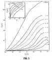
- FIG. 3is a graph of the partial electrical breakdown of a multi-walled nanotube at constant voltage over time
- FIG. 4 ais a graph showing the low bias conductance alternatives between semiconducting and metallic behaviors due to the charging nature of the outermost shell of a multi-walled nanotube at each stage of breakdown;
- FIG. 4 bis a graph showing the conductance of the remaining semiconducting shells after the last metallic shell has been removed from a multi-walled nanotube;
- FIG. 4 cis a table showing the relationship between shell number, diameter, and the relative band gap energy
- FIG. 5is a graph showing the current (I) versus voltage for each shell of a multi-walled nanotube
- FIGS. 6 a through 6 dshow several conversions of random mixtures of molecular conductors (nanotubes) into semiconducting field effect transistors;
- FIG. 7 ais a diagram showing an array of electrodes
- FIG. 7 bis a diagram of a single-walled nanotube rope based field effect transistor including a source, drain, and gate;
- FIG. 8is a flow chart of a method of forming p-type and n-type field effect transistors according to an embodiment of the present invention.
- FIGS. 9 a and 9 bare diagrams of an nanotube-based inverter according to an embodiment of the present invention.
- a method of permanently modifying a multi-walled nanotube (MWNT) or a single-walled nanotube (SWNT) rope or bundleis provided.
- a nanotubecan be metallic or semiconductor depending on its chirality (i.e., conformational geometry). Both species are found in MWNTs and SWNTs.
- a method according to the present inventionuses current-induced electrical breakdown to eliminate individual nanotubes having a particular characteristic. The method is able to tailor the properties of a composite nanotube by changing the proportion of component nanotubes. It should be noted that while the present invention is described using carbon based nanotubes, the illustrative methods are applicable to any molecular structure in which a current can be applied selectively to particular surface areas. For example, the present invention can also be used in Boron-Nitride (BN) and metal dichalcogenids (MX 2 ) based nanostructures.
- BNBoron-Nitride
- MX 2metal dichalcogenids
- Carbon nanotubescan withstand current densities exceeding 10 9 A/cm 2 , in part due to the strength of carbon-to-carbon bonds (e.g., the bond strength for a single C—C bond is about 347 kJ/mol). Ultimately however, at high enough currents, nanotubes will fail. For example, for a MWNT, failure occurs in air at a certain threshold power, e.g., approximately 500:W, above which the rapid oxidation of the outermost carbon shell is initiated.
- a certain threshold powere.g., approximately 500:W, above which the rapid oxidation of the outermost carbon shell is initiated.
- poweris equal to current times the potential difference (i.e., voltage). Because heat induced oxidation of defect-free graphite only proceeds at extremely high temperatures, e.g., >2000 N C, the primary factor in the breakdown initiation according to the present invention is current-induced defect formation, with self-heating being a secondary effect.
- a nanotube 102includes a hexagonal lattice of carbon or other molecules.
- a ring 104can be built including six carbons covalently bonded to one another.
- FIG. 1 bshows an individual carbon ring, each intersection 106 indicates an individual carbon atom, bonds are also indicated as 107 .
- An alternative structureis a boron-nitride ring, one form is shown in FIG. 1 c.
- the boron-nitride ringmay includes three boron atoms, e.g., 110 , bonded to three nitrogen atoms, e.g., 108 , in an alternating pattern.
- a method according to the present inventionselectively breaks current-carrying nanotubes without affecting parallel nanotubes in cases where the parallel nanotubes carry little or no current.
- MWNTsas shown in FIG. 2 a, favor the outermost shell 102 because it is in direct contact with external electrodes (e.g., a source and a drain). This distribution can leave the innermost shells carrying little or no current, which protects them during current-induced oxidation.
- individual nanotubese.g., 102
- the distribution of current through a SWNT ropeis more uniform than through a MWNT because the individual nanotubes of a SWNT rope can be simultaneously in good contact with the external electrodes.
- an electrostatically coupled gate electrodecan selectively deplete the component semiconducting nanotubes of their carriers.
- a SWNT or MWNTwhich spans a source electrode and a drain electrode
- carrierscan be depleted from the component semiconducting nanotubes.
- the semiconducting nanotubesare protected from damage, and high current densities applied to the SWNT or MWNT by the source electrode can be used to initiate oxidation of the component metallic nanotubes.
- these methodscan protect semiconducting nanotubes within a SWNT rope as well as an outer semiconducting MWNT shell.
- the partial electrical breakdown of a MWNT at constant voltage stressproceeds in a series of discrete steps corresponding to the loss of eight individual layers of the MWNT. These results were obtained at a power of about 450:W, and a potential difference of about 2 volts.
- the regular breakdown in current of about 19 ⁇ A per shellcan also be seen in FIG. 5.
- a decrease in radius of a partially broken MWNTis equal to the intershell spacing (0.34 nm) times the number of completed breakdown steps.
- a similar thinningcan be accomplished with a SWNT bundle with metallic SWNTs being selectively broken leaving only the semiconducting SWNTs.
- the breakdownis aided by the sensitivity of nanotubes to external stresses, since relatively small electric fields and currents can affect individual molecules.
- a semiconducting nanotube 1 nm in diametercan be electrostatically depleted of electrical carriers by a gate electrode hundreds of nanometers away.
- the current densityacts as a catalyst, initiating a chemical reaction between the nanotube and surrounding gasses.
- the reactioncan be written as: C (nanotube)+O 2 (gas) à CO 2 (gas).
- the present inventionalso contemplates other environments, wherein nondestructive current-assisted reactions can chemically modify particular nanotubes.
- the resulting devicescould incorporate both electrical switching and chemical sensitivity.
- chemical modificationcan be used in the context of a chemical nanosensor, where a change in the conductivity of a nanosensor (nanotube) signals the presence of a particular gas.
- the controlled destruction of nanotubesallows for the separation of semiconducting SWNTs from mixtures of SWNTs (including metallic and semiconducting SWNTs) and the preparation of nanotube-based field effect transistors (FETs) and inverters.
- FETsfield effect transistors
- the methods disclosed hereincan be used to prepare transistors (e.g., a FET), inverters, diodes, and resistors, depending on the characteristics of the nanotubes and the design of the substrate.
- the processcan facilitate the study of the complex electronic structures and transport properties of MWNTs and SWNT ropes.
- these composite nanowiresmay be re-characterized upon the loss of each constituent conductor (nanotube).
- Characterizationrefers to, for example, the conductance properties of a MWNT or SWNT rope from one stage in the breakdown process to another.
- Multiple complementary transport measurementscan, for example, probe deeper and deeper into the inner shells of a MWNT, allowing for the characterization, as well as a direct comparison, of transports through each shell.
- the different shells of a MWNTare presumed to alternate in a random fashion between metallic and semiconducting. This can be directly tested by using controlled breakdown followed by low bias or low temperature measurements, which probe the outermost shell of a MWNT. Following previous measurements on SWNTs, the semiconducting and metallic shells can be differentiated by measuring the conductance G as a function of gate voltage Vg using a relatively small, 10 mV source-drain bias.
- a metallic shellis characterized by a G which is independent of Vg, or nearly so, whereas a semiconducting shell can be electrostatically depleted of carriers by the gate.
- FIGS. 4 a through 4 cby halting the stress upon each breakdown event, a MWNT may be characterized after the loss of each constituent shell.
- FIG. 4 ashows the low bias conductance (G(Vg)) alternates between semiconducting (e.g., 402 and 406 ) and metallic (e.g., 404 ) behaviors due to the changing nature of the outermost shell at each stage of breakdown.
- G(Vg)the low bias conductance
- n-9when the last metallic shell (n-9) has been removed, the remaining semiconducting shells can be completely depleted to give regions of zero conductance.
- the band gaps of different shellscan be determined within a constant or proportionality.
- the relative widthsagree with calculations based on the expected diameter dependence as shown in FIG. 4 c, in which the only parameters are the initial diameter of the tube and the 0.34 nm spacing between adjacent shells.
- FIGS. 4 a through 4 cshow the room temperature G(Vg) for various different layers within a MWNT.
- the MWNThas a diameter of 9.5 nm, n shells, and a metallic G(Vg).
- FIG. 4 ashows the strong modulation in G(Vg) observed after removing three shells 402 . Removing a fourth layer results in a metallic G(Vg) 404 , and removing the sixth shell produces another semiconducting G(Vg) 406 . This variation is interpreted as a signature of the alternating character of the carbon shells being removed.
- the MWNTUpon removing the tenth carbon shell, the MWNT begins to behave like a perfect, intrinsic field-effect transistor (FET), with a region of zero conductance even at room temperature due to the complete depletion of carriers (e.g., FIG. 4 b ). Similar characteristics are found for individual semiconducting SWNTs, though the SWNTs used were strongly p-type and did not have symmetric G(Vg) characteristics. The complete depletion of the MWNT indicates that no metallic shells remain, and this behavior persists until the fourteenth carbon shell is removed, at which time the MWNT circuit opens. Based on the known intershell spacing of nearly 0.34 nm, a MWNT of this diameter can have at most fourteen shells, in agreement with the shell-by-shell count.
- FETfield-effect transistor
- FIG. 4 bshows the gradual increase of the zero conductance region as the final semiconducting shells are removed.
- a characteristic of semiconducting carbon nanotubesis that the band gap energy is inversely proportional to diameter, so that progressively smaller carbon shells exhibit larger band gaps, the width of the band gap determining the type of material (conductor, semiconductor, insulator).
- the expected ratios between band gap of the innermost shellscan be calculated. As shown in FIG. 4 c, these ratios agree with the experimental ratios, as defined by the conductance peaks on either side of the conductance gap and indicated in FIG. 4 c.
- each shellsaturates at the same current, and that all shells contribute to conduction at moderate and high bias.
- the dashed lineindicates the position of an I-V which was not acquired.
- a semilog plot of selected I-Vsindicates a tendency towards exponential I-Vs for the innermost shells due to the effective barrier between them and the external electrodes. Similar barriers likely play a role in all shells except the outermost one, and explain the nonlinearities observed in some MWNTs but not others.
- FIG. 5shows a sequence of high bias current-voltage characteristics (I-Vs), effectively re-characterizing the MWNT with n, n-1, n-2, etc. shells, until only a single shell remains.
- High bias I-Vsmust be acquired in high vacuum, e.g., ⁇ 1 millibar or in an inert environment, to suppress destructive oxidation. Between each curve, the MWNT was exposed to air in order to controllably remove single carbon shells.
- Four-probe and two-probe measurementswere periodically compared to monitor the contact resistance (Rc) to each nanotube. The data shown here are for samples exhibiting constant Rc of a few kOhms throughout the series of measurements.
- the sequence of I-Vs in FIG. 5also exhibits increasing nonlinearity as shells are removed.
- a tunneling barrierdominates the I-V of the innermost shells, most likely because these shells can only couple to the external electrodes through a barrier composed of many graphitic layers.
- the unusual shape of the measured I-Vscan be understood qualitatively as due to a depth-dependent barrier in series with a nanotube's intrinsic, longitudinal I-V characteristic.
- FIGS. 4 and 5confirm the varying nature of MWNT shells, quantitatively address the coupling between these shells, and attempt to isolate the contribution of a single shell to the overall conductance.
- theory and experimenthave been divided over these issues.
- MWNTsare too complex to realistically model theoretically, and on the other hand no experiments have been able to directly probe the inner carbon shells.
- the powerful technique of controlled breakdown introduced herehas the potential to provide new insights into the transport properties of these complex conductors.
- a MWNTcan be selectively converted between metal and semiconductors with different band gaps.
- SWNTsexhibit some differences.
- multiple SWNTs within a ropecan be in contact with their potentially oxidizing environment, allowing the simultaneous failure of many carbon shells rather than the uniform, shell-by-shell failure observed in a MWNT (e.g., FIG. 3).
- the SWNTs within a ropedo not electrostatically shield each other as effectively as the shells of a MWNT.
- the breakdown in a ropecan be directed solely at the metallic SWNTs by depleting the semiconducting SWNTs of carriers (in this case, Vg is held at +10V during the stress to deplete the predominantly p-type SWNTs of carriers).
- Carrier densities in carbon based SWNTscan range from about 100 to about 1000 electrons/:m. Another difference is that each SWNT in a small rope connects independently to the external electrodes.
- the semiconductorsare depleted of carriers in the selective breakdown of the metallic SWNTs.
- the initial SWNT bundles 602 and 606include both metallic and semiconducting SWNTs, while the thinned SWNT bundles 604 and 608 include far higher proportions of semiconducting SWNTs.
- semiconducting nanotube shells of MWNTscan be effectively insulated be depleting the shells of carriers using similar methods as those for SWNTs.
- desired characteristicse.g., metallic or semiconducting
- the selective breakdown of a composite nanotubecan be explained by the relative dependencies of metallic and semiconducting nanotubes on a gate voltage.
- the conductance of metallic nanotubesshow little dependence on gate voltages, however, the conductance of semiconducting nanotubes exhibit a strong dependence on gate voltage.
- FIGS. 6 a and 6 bdepict G(Vg) for two small SWNT ropes before and after controlled breakdown respectively.
- the unperturbed sampleshave a conductance which can be partially modulated by the gate electrode, much like the case for MWNTs.
- the underlying conductance G mdecreases to zero.
- the extent of modulation G sdoes not change.
- the measurementsindicate that, by depleting the semiconducting SWNTs of carriers during the breakdown process, they can be effectively protected from damage. This result suggests little electronic interaction between different SWNTs in a rope. Measurements of changes in the temperature dependence of G(Vg) could address the issue of interactions and determine at what energy range, if any, such interactions becomes important.
- SWNT FETshave been fabricated individually. Typically, very low surface coverage has ensured that at most one SWNT connects a source and drain electrode at this density, most prospective circuits remain disconnected but some incorporate a metallic SWNT while others have a semiconducting SWNT.
- each padincludes a source 704 , drain 706 , or gate electrode 702 .
- the substrate for these padscan be any insulating material, preferably silica based.
- the combination of substrate and metallic padsis referred to as the substrate for the nanotubes.
- Each FETincludes a source, a drain, a gate, and at least one nanotube connecting the source and the drain. The nanotubes are provided to connect each source to a corresponding drain.
- a gate oxide 708separates the gate 702 from the electrodes ( 704 , 706 ).
- the SWNT densitycan be adjusted to ensure that at least one rope (e.g., 710 ) shorts every set of electrodes while minimizing the unwanted connections between devices.
- the density of nanotubeshas no thickness, e.g., is less than a monolayer or 100% coverage. Some results have shown that densities of less than one percent are sufficient to ensure that each source-drain pair is connected by at least one nanotube, though densities as low as about ⁇ fraction (1/10) ⁇ th of one percent of the substrate can also provide connectivity for each source-drain pair in an array.
- Ropes between source and drain electrodes (e.g., 710 )are converted into FETs by selective breakdown of metallic nanotubes, while stray nanotubes were removed entirely by complete breakdown.
- FIG. 6 dsummarizes results for thirty-two devices incorporating one or more SWNT ropes. Before modification, e.g., 610 , the conductance of individual ropes varies widely due to the distribution of rope sizes as well as contact effects, and very few devices can be substantially depleted by the gate.
- Nanotube FETs exposed to aircan become p-type FETs, i.e., they conduct with holes.
- the nanotube devicescan be made p-type or n-type depending on a method applied to make the contacts.
- the nanotubescan be deposited or grown 800 , selectively broken and cleaned 802 prior to deposition of the metal contacts. Cleaning 802 can be done prior to the lithography 804 .
- Block 804comprises depositing a resist layer over the substrate so that a portion of the nanotube is exposed. The exposed portion can also be cleaned as in block 802 .
- the exposed portion of nanotubeis in a gas 806 .
- the gascan be, for example, air, or gas comprising Oxygen, wherein the gas modifies the conformation of the nanotube and the nanotube behaves as a p-type conductor.
- Metal contactscan be deposited and the resist removed by lift off 808 .
- a gate oxidecan be deposited over the device 810 .
- a metal top gatecan be deposited by, for example, lithography and etch 812 .
- the resulting FETis p-type.
- the deviceis thermally annealed, for example, in a vacuum or an inert gas 814 .
- the metal contactscan be deposited before exposure to air and the resist can be removed by lift off 816 .
- the devicecan be thermally annealed a second time 818 .
- a gate oxidecan be deposited over the device 820 before exposure to the air.
- a metal top gatecan be deposited by, for example, lithography and etch 822 .
- the resulting FETis n-type.
- the nanotubescan be broken prior to deposition of the metal contacts. Accordingly, temporary contacts can be implemented. These temporary contacts are used to break the nanotube. After the nanotubes are broken to a degree where the nanotubes exhibit a desired characteristic, the temporary metal contacts can be removed and the nanotubes cleaned, as shown in block 802 of FIG. 8.
- FIGS. 9 a and 9 ban illustrative diagram of a two SWNT-based voltage inverter 900 .
- This invertercomprises two FETs 902 , 904 .
- a first p-FET 902comprises contacts of a first type 906 .
- a second n-FET (n-FET) 904comprises contacts, e.g., 908 , of a second type.
- the contacts 906 and 908can be made using any metal-nanotube junction.
- the contacts of the n-FET, e.g., 908are out gassed, wherein oxygen is removed.
- the contacts of the p-FET, e.g., 906are exposed to air.
- Each FETcan be produced by electrical breakdown of SWNTs and/or MWNTs, e.g., 910 .
- An external fieldcan be controlled using the gate metal 914 and 916 separated by an insulator 918 , e.g., an oxide, a dielectric gate oxide, an IK dielectric (e.g., a dielectric having a high dielectric constant), or a low temperature oxide.
- a constant potential difference between metal 914 and 916can be obtained by a choice of two metals with different work functions, e.g., Titanium (Ti) and Tungsten (W), so that the threshold voltages of the n-type and p-type FETs overlap.
- the inverterscan be formed on separate substrates as shown in FIG. 9 b.
- the inverter 900can be built using an annealing process in a vacuum. Two FETs can be bonded together to build the inverter 900 . A first FET can be protected by a resist, for example, PMMA or an oxide. A second FET is unprotected. After annealing in vacuum, both FETs are fully n-type. The device can then be exposed to low oxygen pressure, for example, 10 ⁇ 1 Torr. The unprotected FET is back-converted to its original p-type character while the protected FET remains unaffected (e.g., n-type). Combining these two FETs produces a voltage inverter.
- a resistfor example, PMMA or an oxide.
- a second FETis unprotected. After annealing in vacuum, both FETs are fully n-type. The device can then be exposed to low oxygen pressure, for example, 10 ⁇ 1 Torr. The unprotected FET is back-converted to its original p-type character while the
Landscapes
- Engineering & Computer Science (AREA)
- Chemical & Material Sciences (AREA)
- Nanotechnology (AREA)
- Materials Engineering (AREA)
- Theoretical Computer Science (AREA)
- Crystallography & Structural Chemistry (AREA)
- Physics & Mathematics (AREA)
- Mathematical Physics (AREA)
- Thin Film Transistor (AREA)
- Carbon And Carbon Compounds (AREA)
- Superconductors And Manufacturing Methods Therefor (AREA)
- Manufacture Of Switches (AREA)
- Electrodes Of Semiconductors (AREA)
Abstract
Description
- This is a continuation-in-part of Application Ser. No. 09/753,845, entitled “METHODOLOGY FOR ELECTRICALLY INDUCED SELECTIVE BREAKDOWN OF NANOTUBES,” filed Jan. 3, 2001.[0001]
- 1. Field of the Invention[0002]
- The present invention relates to nanostructures, and more particularly to a system and method of electrically induced breakdown of nanostructures.[0003]
- 2. Description of Related Art[0004]
- In the field of molecular nanoelectronics, few materials show as much promise as nanotubes, and in particular carbon nanotubes, which comprise hollow cylinders of graphite, angstroms in diameter. Nanotubes can be made into tiny electronic devices such as diodes and transistors, depending on the nanotube's electrical characteristics. Nanotubes are unique for their size, shape, and physical properties. Structurally a carbon nanotube resembles a hexagonal lattice of carbon rolled into a cylinder.[0005]
- Besides exhibiting intriguing quantum behaviors at low temperature, carbon nanotubes exhibit at least two important characteristics: a nanotube can be either metallic or semiconductor depending on its chirality (i.e., conformational geometry). Metallic nanotubes can carry extremely large current densities with constant resistivity. Semiconducting nanotubes can be electrically switched on and off as field-effect transistors (FETs). The two types may be covalently joined (sharing electrons). These characteristics point to nanotubes as excellent materials for making nanometer-sized semiconductor circuits.[0006]
- Current methods of studying nanotubes rely on the random formation of both metallic and semiconducting nanotubes. There is no known method for reliably preparing a nanotube having particular characteristics, much less for preparing nanotubes to exhibit junctional behavior such as transistors, diodes, etc. Nor are there known methods of nanotube separation by selective synthesis or post-synthesis which have proven to have any measurable level of success. Heretofore, nanotubes must have either been individually separated from mixtures of metallic and semiconducting nanotubes or randomly placed over an electrode to be studied. However, there is no observable consistency in such methods.[0007]
- This lack of control, compounded by nanotubes tendency to bundle together, has hindered the study of nanotube physics and is seen as a primary roadblock in the nanotube development including nanotube-based electronic technology. Therefore, a need exists for a system and method of preparing nanotubes having desired characteristics.[0008]
- A method for forming a device comprises providing a substrate, and providing a plurality of nanotubes in contact with the substrate. The method comprises depositing metal contacts on the substrate, wherein the metal contacts are in contact with a portion of at least one nanotube. The method further comprises selectively breaking the at least one nanotube using an electrical current, removing the metal contacts, and cleaning a remaining nanotube, and depositing a first metal contact in contact with a first end of the nanotube and a second metal contact in contact with a second end of the nanotube.[0009]
- The method further comprises connecting a first metal contact of a first device to a first metal contact of a second device, connecting a substrate of the first device with a substrate of a second device, connecting a second metal contact of the first device to a first voltage, and connecting a second metal contact of the second device to a second voltage. The first device is a p-type field effect transistor and the second device is an n-type field effect transistor. The method comprises depositing a resist over the n-type field effect transistor. The method comprises providing an external potential to the substrate of the first device and the substrate of the second device.[0010]
- The method further comprises the step of depleting a semiconducting nanotube of a plurality of carriers. Depleting a semiconducting nanotube of a plurality of carriers further comprises the step of applying a voltage to a gate electrode on the substrate. The method comprises applying the electrical current through the nanotube from a source electrode to a drain electrode.[0011]
- The plurality of nanotubes are multi-walled nanotubes including metallic and semiconducting nanotubes. The plurality of nanotubes are single-walled nanotube ropes including metallic and semiconducting nanotubes.[0012]
- The substrate is an insulator and includes an array of metallic pads. The substrate is silica based and includes the array of metallic pads. Each pad includes one of a source electrode, a drain electrode, and a gate electrode.[0013]
- Providing a substrate is accomplished using lithography to form an array of pads, each pad including a corresponding electrode on an insulating substrate.[0014]
- The nanotubes are carbon nanotubes.[0015]
- The method comprises breaking a plurality of stray nanotubes.[0016]
- A method for forming a p-type field effect transistor device comprising providing an insulating substrate, and providing a plurality of carbon nanotube bundles including metallic and semiconducting component nanotubes in contact with the substrate. The method comprises breaking the carbon nanotube bundles, cleaning carbon nanotube bundles, and depositing a resist over a portion of the device, wherein a portion of the carbon nanotube bundles is exposed. The method further comprises exposing the portion of the carbon nanotube bundles to a gas, depositing a plurality of metal contacts, and removing the resist. The method deposits a gate oxide over the device, and deposits a top gate metal contact.[0017]
- The gas modifies the conformation of the nanotube to behave as a p-type nanotube.[0018]
- The method comprises connecting the p-type field effect transistor device to an n-type field effect transistor device to form an inverter device.[0019]
- The p-type field effect transistor is formed on a first substrate and the n-type field effect transistor is formed on a second substrate. The p-type field effect transistor and the n-type field effect transistor are formed on the same substrate.[0020]
- A method for forming an n-type field effect transistor device comprises providing an insulating substrate, providing a plurality of carbon nanotube bundles including metallic and semiconducting component nanotubes in contact with the substrate, and breaking the carbon nanotube bundles. The method further comprises cleaning carbon nanotube bundles, depositing a resist over a portion of the device, wherein a portion of the carbon nanotube bundles is exposed, and annealing the device. The method comprises depositing a plurality of metal contacts, removing the resist, and annealing the device to form n-type nanotubes. The method further comprises depositing a gate oxide over the device, and depositing a top gate metal contact.[0021]
- Annealing the device is implemented in one of a vacuum and an inert gas.[0022]
- The method comprises connecting the n-type field effect transistor device to an p-type field effect transistor device to form an inverter device.[0023]
- Preferred embodiments of the present invention will be described below in more detail, with reference to the accompanying drawings:[0024]
- FIGS. 1[0025]a,1b,and1care diagrams of a nanotube and constituent hexagonal rings;
- FIG. 2[0026]ais a diagram showing a multi-walled nanotube;
- FIG. 2[0027]bis a diagram showing a single-walled nanotube rope;
- FIG. 3 is a graph of the partial electrical breakdown of a multi-walled nanotube at constant voltage over time;[0028]
- FIG. 4[0029]ais a graph showing the low bias conductance alternatives between semiconducting and metallic behaviors due to the charging nature of the outermost shell of a multi-walled nanotube at each stage of breakdown;
- FIG. 4[0030]bis a graph showing the conductance of the remaining semiconducting shells after the last metallic shell has been removed from a multi-walled nanotube;
- FIG. 4[0031]cis a table showing the relationship between shell number, diameter, and the relative band gap energy;
- FIG. 5 is a graph showing the current (I) versus voltage for each shell of a multi-walled nanotube;[0032]
- FIGS. 6[0033]athrough6dshow several conversions of random mixtures of molecular conductors (nanotubes) into semiconducting field effect transistors;
- FIG. 7[0034]ais a diagram showing an array of electrodes;
- FIG. 7[0035]bis a diagram of a single-walled nanotube rope based field effect transistor including a source, drain, and gate;
- FIG. 8 is a flow chart of a method of forming p-type and n-type field effect transistors according to an embodiment of the present invention; and[0036]
- FIGS. 9[0037]aand9bare diagrams of an nanotube-based inverter according to an embodiment of the present invention.
- According to the present invention a method of permanently modifying a multi-walled nanotube (MWNT) or a single-walled nanotube (SWNT) rope or bundle is provided. A nanotube can be metallic or semiconductor depending on its chirality (i.e., conformational geometry). Both species are found in MWNTs and SWNTs. A method according to the present invention uses current-induced electrical breakdown to eliminate individual nanotubes having a particular characteristic. The method is able to tailor the properties of a composite nanotube by changing the proportion of component nanotubes. It should be noted that while the present invention is described using carbon based nanotubes, the illustrative methods are applicable to any molecular structure in which a current can be applied selectively to particular surface areas. For example, the present invention can also be used in Boron-Nitride (BN) and metal dichalcogenids (MX[0038]2) based nanostructures.
- Carbon nanotubes can withstand current densities exceeding 10[0039]9A/cm2, in part due to the strength of carbon-to-carbon bonds (e.g., the bond strength for a single C—C bond is about 347 kJ/mol). Ultimately however, at high enough currents, nanotubes will fail. For example, for a MWNT, failure occurs in air at a certain threshold power, e.g., approximately 500:W, above which the rapid oxidation of the outermost carbon shell is initiated. Remember that power is equal to current times the potential difference (i.e., voltage). Because heat induced oxidation of defect-free graphite only proceeds at extremely high temperatures, e.g., >2000NC, the primary factor in the breakdown initiation according to the present invention is current-induced defect formation, with self-heating being a secondary effect.
- Referring to FIG. 1[0040]a,a
nanotube 102 includes a hexagonal lattice of carbon or other molecules. In the case of carbon, aring 104 can be built including six carbons covalently bonded to one another. FIG. 1bshows an individual carbon ring, eachintersection 106 indicates an individual carbon atom, bonds are also indicated as107. An alternative structure is a boron-nitride ring, one form is shown in FIG. 1c.The boron-nitride ring may includes three boron atoms, e.g.,110, bonded to three nitrogen atoms, e.g.,108, in an alternating pattern. - By taking advantage of the current-induced defect formation, a method according to the present invention selectively breaks current-carrying nanotubes without affecting parallel nanotubes in cases where the parallel nanotubes carry little or no current. For example, MWNTs as shown in FIG. 2[0041]a,favor the
outermost shell 102 because it is in direct contact with external electrodes (e.g., a source and a drain). This distribution can leave the innermost shells carrying little or no current, which protects them during current-induced oxidation. In a SWNT rope, shown in FIG. 2b,individual nanotubes (e.g.,102) are arranged in parallel. The distribution of current through a SWNT rope is more uniform than through a MWNT because the individual nanotubes of a SWNT rope can be simultaneously in good contact with the external electrodes. - Generally there is no reason for a current to favor some SWNTs over others, however, according to an embodiment of the present invention, an electrostatically coupled gate electrode can selectively deplete the component semiconducting nanotubes of their carriers. In other words, for a SWNT or MWNT which spans a source electrode and a drain electrode, by applying a voltage to a corresponding gate electrode, carriers can be depleted from the component semiconducting nanotubes. Once depleted, the semiconducting nanotubes are protected from damage, and high current densities applied to the SWNT or MWNT by the source electrode can be used to initiate oxidation of the component metallic nanotubes. Thus, these methods can protect semiconducting nanotubes within a SWNT rope as well as an outer semiconducting MWNT shell.[0042]
- The removal of carbon nanotubes from these composite conductors can be observed both electrically and through microscopy. Electrically, the breakdown of a single carbon nanotube results in a partial conductance drop, typically completed in a few milliseconds. When stressed at sufficiently high bias, multiple independent drops occur as one carbon shell after another is broken. The electronics used in the breakdown are capable of controlling the number of nanotubes broken. Upon sensing a drop in current, e.g., about 19 :A, the electronics are able to stop the breakdown process, thereby controlling the exhibited characteristics.[0043]
- Referring to FIG. 3, the partial electrical breakdown of a MWNT at constant voltage stress proceeds in a series of discrete steps corresponding to the loss of eight individual layers of the MWNT. These results were obtained at a power of about 450:W, and a potential difference of about 2 volts. The regular breakdown in current of about 19 μA per shell can also be seen in FIG. 5. A decrease in radius of a partially broken MWNT is equal to the intershell spacing (0.34 nm) times the number of completed breakdown steps. A similar thinning can be accomplished with a SWNT bundle with metallic SWNTs being selectively broken leaving only the semiconducting SWNTs.[0044]
- The breakdown is aided by the sensitivity of nanotubes to external stresses, since relatively small electric fields and currents can affect individual molecules. For example, a[0045]
semiconducting nanotube 1 nm in diameter can be electrostatically depleted of electrical carriers by a gate electrode hundreds of nanometers away. The current density (sufficient to affect nanotube breakdown) acts as a catalyst, initiating a chemical reaction between the nanotube and surrounding gasses. For example, for a carbon nanotube in air, the reaction can be written as: C (nanotube)+O2(gas) à CO2(gas). - The present invention also contemplates other environments, wherein nondestructive current-assisted reactions can chemically modify particular nanotubes. The resulting devices could incorporate both electrical switching and chemical sensitivity. For example, using a nanotube's sensitivity to various gases, chemical modification can be used in the context of a chemical nanosensor, where a change in the conductivity of a nanosensor (nanotube) signals the presence of a particular gas.[0046]
- On a practical level, the controlled destruction of nanotubes allows for the separation of semiconducting SWNTs from mixtures of SWNTs (including metallic and semiconducting SWNTs) and the preparation of nanotube-based field effect transistors (FETs) and inverters. It should also be noted that, the methods disclosed herein can be used to prepare transistors (e.g., a FET), inverters, diodes, and resistors, depending on the characteristics of the nanotubes and the design of the substrate.[0047]
- More fundamentally, the process can facilitate the study of the complex electronic structures and transport properties of MWNTs and SWNT ropes. By removing the stress (current) at the occurrence of individual conductance steps, these composite nanowires may be re-characterized upon the loss of each constituent conductor (nanotube). Characterization refers to, for example, the conductance properties of a MWNT or SWNT rope from one stage in the breakdown process to another. Multiple complementary transport measurements can, for example, probe deeper and deeper into the inner shells of a MWNT, allowing for the characterization, as well as a direct comparison, of transports through each shell.[0048]
- The different shells of a MWNT are presumed to alternate in a random fashion between metallic and semiconducting. This can be directly tested by using controlled breakdown followed by low bias or low temperature measurements, which probe the outermost shell of a MWNT. Following previous measurements on SWNTs, the semiconducting and metallic shells can be differentiated by measuring the conductance G as a function of gate voltage Vg using a relatively small, 10 mV source-drain bias. A metallic shell is characterized by a G which is independent of Vg, or nearly so, whereas a semiconducting shell can be electrostatically depleted of carriers by the gate.[0049]
- Referring to FIGS. 4[0050]athrough4c,by halting the stress upon each breakdown event, a MWNT may be characterized after the loss of each constituent shell. FIG. 4ashows the low bias conductance (G(Vg)) alternates between semiconducting (e.g.,402 and406) and metallic (e.g.,404) behaviors due to the changing nature of the outermost shell at each stage of breakdown. In FIG. 4b,when the last metallic shell (n-9) has been removed, the remaining semiconducting shells can be completely depleted to give regions of zero conductance. Taking the indicated peaks in G(Vg) to correspond to conductance and valence band edges, the band gaps of different shells can be determined within a constant or proportionality. The relative widths agree with calculations based on the expected diameter dependence as shown in FIG. 4c,in which the only parameters are the initial diameter of the tube and the 0.34 nm spacing between adjacent shells.
- FIGS. 4[0051]athrough4cshow the room temperature G(Vg) for various different layers within a MWNT. Initially, the MWNT has a diameter of 9.5 nm, n shells, and a metallic G(Vg). FIG. 4ashows the strong modulation in G(Vg) observed after removing three
shells 402. Removing a fourth layer results in a metallic G(Vg)404, and removing the sixth shell produces another semiconducting G(Vg)406. This variation is interpreted as a signature of the alternating character of the carbon shells being removed. - The fact that G does not fall to zero for a particular semiconducting shell is due to the contribution of inner metallic shells which continue to conduct. Shells n-3 and n-4 demonstrate this: the depletion minimum of the G(Vg) curve for shell n-3 coincides with the conductance of the underlying shell n-4[0052]408. In this case, the outer, semiconducting shell n-3 can be fully depleted by the gate, but the measured conductance includes leakage through the underlying metallic shell. Additional measurements show that this leakage is energetically frozen out in the low temperature, the low bias limit indicating that the intershell coupling is thermally activated. The gradual thinning of MWNTs and SWNT ropes can be resolved using, for example, atomic force and scanning electron microscopy with a linear correspondence between the number of breakdown steps and change in apparent diameter.
- Upon removing the tenth carbon shell, the MWNT begins to behave like a perfect, intrinsic field-effect transistor (FET), with a region of zero conductance even at room temperature due to the complete depletion of carriers (e.g., FIG. 4[0053]b). Similar characteristics are found for individual semiconducting SWNTs, though the SWNTs used were strongly p-type and did not have symmetric G(Vg) characteristics. The complete depletion of the MWNT indicates that no metallic shells remain, and this behavior persists until the fourteenth carbon shell is removed, at which time the MWNT circuit opens. Based on the known intershell spacing of nearly 0.34 nm, a MWNT of this diameter can have at most fourteen shells, in agreement with the shell-by-shell count.
- FIG. 4[0054]bshows the gradual increase of the zero conductance region as the final semiconducting shells are removed. The width of this region is proportional to the band gap (the energy needed to break a bond) of the semiconductors, with conduction above and below the gap due to electron-like and hole-like carriers, respectively. Due to the use of high voltage pulses to break shells, some rearrangement of trapped charges occurs on an underlying SiO2substrate. To simplify the comparison among shells, the curve shown in FIG. 4bis centered near Vg=0. A characteristic of semiconducting carbon nanotubes is that the band gap energy is inversely proportional to diameter, so that progressively smaller carbon shells exhibit larger band gaps, the width of the band gap determining the type of material (conductor, semiconductor, insulator). Using only the initial MWNT diameter and the intershell spacing, the expected ratios between band gap of the innermost shells can be calculated. As shown in FIG. 4c,these ratios agree with the experimental ratios, as defined by the conductance peaks on either side of the conductance gap and indicated in FIG. 4c.
- Referring now to FIG. 5, by recharacterizing the MWNT after the loss of individual shells, the contribution of each shell to the I-V can be determined. Based on the uniform spacing of the sequence of I-Vs, each shell saturates at the same current, and that all shells contribute to conduction at moderate and high bias. The dashed line indicates the position of an I-V which was not acquired. A semilog plot of selected I-Vs indicates a tendency towards exponential I-Vs for the innermost shells due to the effective barrier between them and the external electrodes. Similar barriers likely play a role in all shells except the outermost one, and explain the nonlinearities observed in some MWNTs but not others.[0055]
- FIG. 5 shows a sequence of high bias current-voltage characteristics (I-Vs), effectively re-characterizing the MWNT with n, n-1, n-2, etc. shells, until only a single shell remains. High bias I-Vs must be acquired in high vacuum, e.g., <1 millibar or in an inert environment, to suppress destructive oxidation. Between each curve, the MWNT was exposed to air in order to controllably remove single carbon shells. Four-probe and two-probe measurements were periodically compared to monitor the contact resistance (Rc) to each nanotube. The data shown here are for samples exhibiting constant Rc of a few kOhms throughout the series of measurements. Samples with high Rc tend to fail at the contact, as opposed to the shell-by-shell mechanism described herein. Each I-V shows current saturation at a steadily increasing bias, similar to that observed in individual SWNTs, but at much higher currents. The removal of each shell from the MWNT appears to decrease this saturation level by a fixed amount of approximately 20 μA, in agreement with FIG. 3. This step-by-step decrease clearly indicates a high bias, that all of the MWNT shells contribute to transport and saturate equally.[0056]
- Besides the decrease of the current saturation value, the sequence of I-Vs in FIG. 5 also exhibits increasing nonlinearity as shells are removed. A semilog plot of selected IVs shows the trend from a linear I-V towards an exponential characteristic of the form I =A exp(V/V[0057]0), with V0=0.50V. Apparently, a tunneling barrier dominates the I-V of the innermost shells, most likely because these shells can only couple to the external electrodes through a barrier composed of many graphitic layers. For intermediate shells, not in direct contact with the electrodes, the unusual shape of the measured I-Vs can be understood qualitatively as due to a depth-dependent barrier in series with a nanotube's intrinsic, longitudinal I-V characteristic. This series barrier explains the gradual increase of the bias required to reach current saturation shown in FIG. 5. Furthermore, the transition from linear to nonlinear I-Vs observed here, and the abundance of similar nonlinear I-Vs reported in the literature suggests that transport experiments often do not directly contact the current-carrying carbon shell of a MWNT, but rather contact the partial or incomplete shells typically observed by transmission electron microscopy.
- FIGS. 4 and 5 confirm the varying nature of MWNT shells, quantitatively address the coupling between these shells, and attempt to isolate the contribution of a single shell to the overall conductance. Until now, theory and experiment have been divided over these issues. On one hand, MWNTs are too complex to realistically model theoretically, and on the other hand no experiments have been able to directly probe the inner carbon shells. The powerful technique of controlled breakdown introduced here has the potential to provide new insights into the transport properties of these complex conductors. In addition, a MWNT can be selectively converted between metal and semiconductors with different band gaps.[0058]
- The methods described for MWNTs can be applied to SWNT ropes. Although both MWNTs and SWNTs are composite nanotubes, SWNTs exhibit some differences. For example, multiple SWNTs within a rope can be in contact with their potentially oxidizing environment, allowing the simultaneous failure of many carbon shells rather than the uniform, shell-by-shell failure observed in a MWNT (e.g., FIG. 3). In addition, the SWNTs within a rope do not electrostatically shield each other as effectively as the shells of a MWNT. As a result, the breakdown in a rope can be directed solely at the metallic SWNTs by depleting the semiconducting SWNTs of carriers (in this case, Vg is held at +10V during the stress to deplete the predominantly p-type SWNTs of carriers). Carrier densities in carbon based SWNTs can range from about 100 to about 1000 electrons/:m. Another difference is that each SWNT in a small rope connects independently to the external electrodes. Thus, more so than for a MWNT, a rope may be modeled as independent, parallel conductors with total conductance G(Vg)=G[0059]m+Gs(Vg), where Gmis the contribution of the metallic nanotubes and Gsis the gate-dependent conductance of the semiconducting nanotubes.
- Referring to FIGS. 6[0060]aand6b,by stressing a SWNT rope including a mixture of semiconducting and metallic SWNTs while simultaneously gating the bundle, the semiconductors are depleted of carriers in the selective breakdown of the metallic SWNTs. The initial SWNT bundles602 and606 include both metallic and semiconducting SWNTs, while the thinned SWNT bundles604 and608 include far higher proportions of semiconducting SWNTs. Likewise, semiconducting nanotube shells of MWNTs can be effectively insulated be depleting the shells of carriers using similar methods as those for SWNTs. Thus the breakdown of a MWNT can be controlled to yield desired characteristics (e.g., metallic or semiconducting). The selective breakdown of a composite nanotube can be explained by the relative dependencies of metallic and semiconducting nanotubes on a gate voltage. The conductance of metallic nanotubes show little dependence on gate voltages, however, the conductance of semiconducting nanotubes exhibit a strong dependence on gate voltage.
- Thus, as shown in FIGS. 6[0061]aand6b,at positive gate voltages, the conductance of the SWNT approaches zero, while at negative gate voltages, the conductance increases as carriers are added. FIGS. 6aand6bdepict G(Vg) for two small SWNT ropes before and after controlled breakdown respectively. The unperturbed samples have a conductance which can be partially modulated by the gate electrode, much like the case for MWNTs. As the metallic SWNTs in the rope are destroyed, the underlying conductance Gmdecreases to zero. In contrast, the extent of modulation Gsdoes not change. The measurements indicate that, by depleting the semiconducting SWNTs of carriers during the breakdown process, they can be effectively protected from damage. This result suggests little electronic interaction between different SWNTs in a rope. Measurements of changes in the temperature dependence of G(Vg) could address the issue of interactions and determine at what energy range, if any, such interactions becomes important.
- With the semiconducting SWNTs unaffected, the G(Vg) curve is rigidly shifted downwards according to the contribution of the metallic SWNTs. Referring to FIG. 6[0062]c,even for very large ropes containing hundreds of SWNTs, these samples can be effectively converted into FETs. However, in this case the gradual decrease of Gmhalts before it reaches zero, presumably because metallic SWNTs at the core of the rope are encased by semiconducting SWNTs. The ultimate destruction of these weakly-coupled metallic SWNTs can require higher voltages and may sacrifice some surrounding semiconducting SWNTs. As a result, a rope with many semiconducting channels and a large, initial modulation Gs>10 μS may only result in a FET with Gs˜1 μS.
- Besides being useful for the study of MWNTs and SWNT interactions, the controlled breakdown technique is extremely valuable for the fabrication of nanotube-based electronic devices. Until now, SWNT FETs have been fabricated individually. Typically, very low surface coverage has ensured that at most one SWNT connects a source and drain electrode at this density, most prospective circuits remain disconnected but some incorporate a metallic SWNT while others have a semiconducting SWNT.[0063]
- While this technique has proven valuable for the initial characterization of SWNT properties, practical applications will need reliable generation of many devices in parallel. Achieving densely packed FETs, for example, needs purely semiconducting SWNTs at a sufficient density to interconnect all of the desired positions. The nanotubes may be provided by known techniques, such as, in-situ growth by chemical vapor deposition or grown ex-situ and deposited. High surface densities favor multiple SWNTs and SWNT ropes which, due to the variability of SWNT properties, are dominated by metallic tubes, useless as semiconducting channels. At present, no method is known to exist for the synthesis of purely semiconducting SWNTs or for the separation of semiconducting SWNTs from SWNT mixtures.[0064]
- Referring to FIG. 7[0065]a,showing a small array of independently addressable SWNT FETs fabricated using standard lithography. An array of metallic pads (e.g.,701) is provided, each pad includes a
source 704, drain706, orgate electrode 702. The substrate for these pads can be any insulating material, preferably silica based. The combination of substrate and metallic pads is referred to as the substrate for the nanotubes. Each FET includes a source, a drain, a gate, and at least one nanotube connecting the source and the drain. The nanotubes are provided to connect each source to a corresponding drain. Referring now to FIG. 7b,agate oxide 708 separates thegate 702 from the electrodes (704,706). The SWNT density can be adjusted to ensure that at least one rope (e.g.,710) shorts every set of electrodes while minimizing the unwanted connections between devices. Preferably, the density of nanotubes has no thickness, e.g., is less than a monolayer or 100% coverage. Some results have shown that densities of less than one percent are sufficient to ensure that each source-drain pair is connected by at least one nanotube, though densities as low as about {fraction (1/10)}th of one percent of the substrate can also provide connectivity for each source-drain pair in an array. Ropes between source and drain electrodes (e.g.,710) are converted into FETs by selective breakdown of metallic nanotubes, while stray nanotubes were removed entirely by complete breakdown. - Although these ropes initially show little or no switching because of their metallic constituents, final devices with good FET characteristics can be reliably achieved as shown in FIG. 6[0066]d.Some results indicate that the generation of SWNT FETs can be achieved with greater than 90% certainty from a disordered starting material. FIG. 6dsummarizes results for thirty-two devices incorporating one or more SWNT ropes. Before modification, e.g.,610, the conductance of individual ropes varies widely due to the distribution of rope sizes as well as contact effects, and very few devices can be substantially depleted by the gate.
- Upon breaking the metallic SWNTs (e.g.,[0067]612), the conductance of each rope is decreased but the remaining channel is solely semiconducting and can be fully depleted. The resulting devices have reasonable FET characteristics limited primarily by contact resistance, a difficulty which is being addressed separately. Multiple, small SWNT bundles can be produced by chemical vapor growth and can alleviate the difficulties encountered with large bundles and result in FETs having excellent conductivity and switching ratios.
- Although this disclosure has focused on the particular system of carbon nanotubes, the same principles may apply broadly to various molecular electronics systems. In general, arrays of molecular devices can be produced by design using external electrical means, without a need for actual control at the nanometer scale. Discretionary modification allows for the definition of useful electronic elements from a random mixture. Although this solution has been applied to solve the problem of variation inherent to carbon nanotubes, one skilled in the art would see in light of the present disclosure that similar results can be achieved using mixtures of other molecules.[0068]
- Nanotube FETs exposed to air can become p-type FETs, i.e., they conduct with holes. Referring to FIG. 8, the nanotube devices can be made p-type or n-type depending on a method applied to make the contacts. The nanotubes can be deposited or grown[0069]800, selectively broken and cleaned802 prior to deposition of the metal contacts. Cleaning802 can be done prior to the lithography804. Block804 comprises depositing a resist layer over the substrate so that a portion of the nanotube is exposed. The exposed portion can also be cleaned as in block802. To make a p-type FET, the exposed portion of nanotube is in a
gas 806. The gas can be, for example, air, or gas comprising Oxygen, wherein the gas modifies the conformation of the nanotube and the nanotube behaves as a p-type conductor. Metal contacts can be deposited and the resist removed by lift off808. A gate oxide can be deposited over thedevice 810. A metal top gate can be deposited by, for example, lithography and etch812. The resulting FET is p-type. For building an n-type FET, after lithography804, the device is thermally annealed, for example, in a vacuum or aninert gas 814. The metal contacts can be deposited before exposure to air and the resist can be removed by lift off816. The device can be thermally annealed asecond time 818. A gate oxide can be deposited over thedevice 820 before exposure to the air. A metal top gate can be deposited by, for example, lithography andetch 822. The resulting FET is n-type. - As stated above, the nanotubes can be broken prior to deposition of the metal contacts. Accordingly, temporary contacts can be implemented. These temporary contacts are used to break the nanotube. After the nanotubes are broken to a degree where the nanotubes exhibit a desired characteristic, the temporary metal contacts can be removed and the nanotubes cleaned, as shown in block[0070]802 of FIG. 8.
- Referring to FIGS. 9[0071]aand9b,an illustrative diagram of a two SWNT-based
voltage inverter 900. This inverter comprises twoFETs FET 902 comprises contacts of afirst type 906. A second n-FET (n-FET)904 comprises contacts, e.g.,908, of a second type. Thecontacts gate metal insulator 918, e.g., an oxide, a dielectric gate oxide, an IK dielectric (e.g., a dielectric having a high dielectric constant), or a low temperature oxide. A constant potential difference betweenmetal FET 902 is turned OFF while the n-FET 904 is ON. No current flows through the device and there is no voltage drop in the n-FET 904. The output voltage is then −V. On the contrary, when a negative input voltage is applied, the p-FET 902 is ON, the n-FET 904 is OFF and the output voltage is +V. In the intermediate region (about V0=0) neither FET is totally ON or OFF. Some current flows through the device and the output voltage is between −V and +V. The inverters can be formed on separate substrates as shown in FIG. 9b. - The[0072]
inverter 900 can be built using an annealing process in a vacuum. Two FETs can be bonded together to build theinverter 900. A first FET can be protected by a resist, for example, PMMA or an oxide. A second FET is unprotected. After annealing in vacuum, both FETs are fully n-type. The device can then be exposed to low oxygen pressure, for example, 10−1Torr. The unprotected FET is back-converted to its original p-type character while the protected FET remains unaffected (e.g., n-type). Combining these two FETs produces a voltage inverter. - Having described embodiments of a method for engineering carbon nanotubes and nanotube circuits using electrical breakdown, it is noted that modifications and variations can be made by persons skilled in the art in light of the above teachings. It is therefore to be understood that changes may be made in the particular embodiments of the invention disclosed which are within the scope and spirit of the invention as defined by the appended claims. Having thus described the invention with the details and particularity required by the patent laws, what is claimed and desired protected by Letters Patent is set forth in the appended claims.[0073]
Claims (25)
Priority Applications (1)
| Application Number | Priority Date | Filing Date | Title |
|---|---|---|---|
| US10/144,402US6706566B2 (en) | 2001-01-03 | 2002-05-13 | Methodology for electrically induced selective breakdown of nanotubes |
Applications Claiming Priority (2)
| Application Number | Priority Date | Filing Date | Title |
|---|---|---|---|
| US09/753,845US6423583B1 (en) | 2001-01-03 | 2001-01-03 | Methodology for electrically induced selective breakdown of nanotubes |
| US10/144,402US6706566B2 (en) | 2001-01-03 | 2002-05-13 | Methodology for electrically induced selective breakdown of nanotubes |
Related Parent Applications (1)
| Application Number | Title | Priority Date | Filing Date |
|---|---|---|---|
| US09/753,845Continuation-In-PartUS6423583B1 (en) | 2001-01-03 | 2001-01-03 | Methodology for electrically induced selective breakdown of nanotubes |
Publications (2)
| Publication Number | Publication Date |
|---|---|
| US20020173083A1true US20020173083A1 (en) | 2002-11-21 |
| US6706566B2 US6706566B2 (en) | 2004-03-16 |
Family
ID=25032396
Family Applications (2)
| Application Number | Title | Priority Date | Filing Date |
|---|---|---|---|
| US09/753,845Expired - LifetimeUS6423583B1 (en) | 2001-01-03 | 2001-01-03 | Methodology for electrically induced selective breakdown of nanotubes |
| US10/144,402Expired - LifetimeUS6706566B2 (en) | 2001-01-03 | 2002-05-13 | Methodology for electrically induced selective breakdown of nanotubes |
Family Applications Before (1)
| Application Number | Title | Priority Date | Filing Date |
|---|---|---|---|
| US09/753,845Expired - LifetimeUS6423583B1 (en) | 2001-01-03 | 2001-01-03 | Methodology for electrically induced selective breakdown of nanotubes |
Country Status (11)
| Country | Link |
|---|---|
| US (2) | US6423583B1 (en) |
| EP (1) | EP1350277B1 (en) |
| JP (1) | JP4099063B2 (en) |
| KR (1) | KR100621444B1 (en) |
| CN (1) | CN100347874C (en) |
| AT (1) | ATE526690T1 (en) |
| CA (1) | CA2431064C (en) |
| IL (2) | IL156523A0 (en) |
| MY (1) | MY127407A (en) |
| TW (1) | TW523797B (en) |
| WO (1) | WO2002054505A2 (en) |
Cited By (69)
| Publication number | Priority date | Publication date | Assignee | Title |
|---|---|---|---|---|
| US20030021966A1 (en)* | 2001-07-25 | 2003-01-30 | Segal Brent M. | Electromechanical memory array using nanotube ribbons and method for making same |
| US20030214054A1 (en)* | 2002-05-20 | 2003-11-20 | Fujitsu Limited | Electron device and process of manufacturing thereof |
| US6706402B2 (en) | 2001-07-25 | 2004-03-16 | Nantero, Inc. | Nanotube films and articles |
| US20040112964A1 (en)* | 2002-09-30 | 2004-06-17 | Nanosys, Inc. | Applications of nano-enabled large area macroelectronic substrates incorporating nanowires and nanowire composites |
| US6762073B1 (en) | 2003-02-24 | 2004-07-13 | Donald P. Cullen | Method of fabricating electronic interconnect devices using direct imaging of dielectric composite material |
| US20040135951A1 (en)* | 2002-09-30 | 2004-07-15 | Dave Stumbo | Integrated displays using nanowire transistors |
| WO2004065655A1 (en)* | 2003-01-13 | 2004-08-05 | Nantero, Inc. | Methods of using thin metal layers to make carbon nanotube films, layers, fabrics, ribbons, elements and articles |
| US6784028B2 (en) | 2001-12-28 | 2004-08-31 | Nantero, Inc. | Methods of making electromechanical three-trace junction devices |
| WO2004076049A3 (en)* | 2003-02-28 | 2004-11-11 | Univ Surrey | Method and apparatus for fabricating nanoscale structures |
| US6836424B2 (en) | 2001-07-25 | 2004-12-28 | Nantero, Inc. | Hybrid circuit having nanotube electromechanical memory |
| US6835591B2 (en) | 2001-07-25 | 2004-12-28 | Nantero, Inc. | Methods of nanotube films and articles |
| WO2005031845A1 (en)* | 2003-09-22 | 2005-04-07 | Lucent Technologies, Inc. | Field-effect transistors with weakly coupled layered inorganic semiconductors |
| US20050079659A1 (en)* | 2002-09-30 | 2005-04-14 | Nanosys, Inc. | Large-area nanoenabled macroelectronic substrates and uses therefor |
| US20050106846A1 (en)* | 2003-10-17 | 2005-05-19 | Dubin Valery M. | Method of sorting carbon nanotubes including protecting metallic nanotubes and removing the semiconducting nanotubes |
| US6911682B2 (en) | 2001-12-28 | 2005-06-28 | Nantero, Inc. | Electromechanical three-trace junction devices |
| US20050166292A1 (en)* | 2003-10-10 | 2005-07-28 | General Electric Company | Free-standing electrostatically-doped carbon nanotube device and method for making same |
| US20050174842A1 (en)* | 2004-02-11 | 2005-08-11 | Nantero, Inc. | EEPROMS using carbon nanotubes for cell storage |
| WO2005038881A3 (en)* | 2003-10-16 | 2005-11-03 | Univ Cambridge Tech | Short-channel transistors |
| US20050250305A1 (en)* | 2004-05-04 | 2005-11-10 | State of Oregon acting by and through the State Board of Higher Education on behalf of | Carbon nanotube (CNT) multiplexers, circuits, and actuators |
| US20060081886A1 (en)* | 2004-10-15 | 2006-04-20 | Nanosys, Inc. | Method, system and apparatus for gating configurations and improved contacts in nanowire-based electronic devices |
| US20060151820A1 (en)* | 2002-09-30 | 2006-07-13 | Nanosys, Inc. | Large-area nanoenabled macroelectronic substrates and uses therefor |
| US20060214192A1 (en)* | 2003-12-08 | 2006-09-28 | Matsushita Electric Industrial Co., Ltd. | Field effect transistor, electrical device array and method for manufacturing those |
| US20060214156A1 (en)* | 2004-10-12 | 2006-09-28 | Nanosys, Inc. | Fully integrated organic layered processes for making plastic electronics based on conductive polymers and semiconductor nanowires |
| US7120047B2 (en) | 2001-07-25 | 2006-10-10 | Segal Brent M | Device selection circuitry constructed with nanotube technology |
| US20060237857A1 (en)* | 2005-01-14 | 2006-10-26 | Nantero, Inc. | Hybrid carbon nanotube FET(CNFET)-FET static RAM (SRAM) and method of making same |
| US20060255834A1 (en)* | 2004-06-18 | 2006-11-16 | Nantero, Inc. | Tri-state circuit using nanotube switching elements |
| US20070001220A1 (en)* | 2004-09-16 | 2007-01-04 | Atomate Corporation | Nanotube Transistor and Rectifying Devices |
| US7176505B2 (en) | 2001-12-28 | 2007-02-13 | Nantero, Inc. | Electromechanical three-trace junction devices |
| US20070102747A1 (en)* | 2005-11-10 | 2007-05-10 | International Business Machines Corporation | Complementary carbon nanotube triple gate technology |
| US20070160842A1 (en)* | 2002-02-08 | 2007-07-12 | Masukazu Hirata | Structure matter of thin-film particles having carbon skeleton, processes for the production of the structure matter and the thin-film particles and uses thereof |
| US20070176824A1 (en)* | 2002-09-30 | 2007-08-02 | Nanosys Inc. | Phased array systems and methods |
| US7265575B2 (en) | 2004-06-18 | 2007-09-04 | Nantero, Inc. | Nanotube-based logic driver circuits |
| US7274064B2 (en) | 2003-06-09 | 2007-09-25 | Nanatero, Inc. | Non-volatile electromechanical field effect devices and circuits using same and methods of forming same |
| US7274078B2 (en) | 2001-07-25 | 2007-09-25 | Nantero, Inc. | Devices having vertically-disposed nanofabric articles and methods of making the same |
| US20070224804A1 (en)* | 2004-03-26 | 2007-09-27 | Thomas Tiano | Carbon nanotube-based electronic devices made by electrolytic deposition and applications thereof |
| US7280394B2 (en) | 2003-06-09 | 2007-10-09 | Nantero, Inc. | Field effect devices having a drain controlled via a nanotube switching element |
| US7289357B2 (en) | 2003-08-13 | 2007-10-30 | Nantero, Inc. | Isolation structure for deflectable nanotube elements |
| US7288970B2 (en) | 2004-06-18 | 2007-10-30 | Nantero, Inc. | Integrated nanotube and field effect switching device |
| US7294877B2 (en) | 2003-03-28 | 2007-11-13 | Nantero, Inc. | Nanotube-on-gate FET structures and applications |
| US7304357B2 (en) | 2001-07-25 | 2007-12-04 | Nantero, Inc. | Devices having horizontally-disposed nanofabric articles and methods of making the same |
| US7335395B2 (en) | 2002-04-23 | 2008-02-26 | Nantero, Inc. | Methods of using pre-formed nanotubes to make carbon nanotube films, layers, fabrics, ribbons, elements and articles |
| US7339401B2 (en) | 2003-08-13 | 2008-03-04 | Nantero, Inc. | Nanotube-based switching elements with multiple controls |
| US7394687B2 (en) | 2005-05-09 | 2008-07-01 | Nantero, Inc. | Non-volatile-shadow latch using a nanotube switch |
| US7405605B2 (en) | 2004-06-18 | 2008-07-29 | Nantero, Inc. | Storage elements using nanotube switching elements |
| US20080272361A1 (en)* | 2007-05-02 | 2008-11-06 | Atomate Corporation | High Density Nanotube Devices |
| US20080292531A1 (en)* | 2006-10-19 | 2008-11-27 | Rensselaer Polytechnic Institute | Electrical current-induced structural changes and chemical functionalization of carbon nanotubes |
| US7479654B2 (en) | 2005-05-09 | 2009-01-20 | Nantero, Inc. | Memory arrays using nanotube articles with reprogrammable resistance |
| US7560136B2 (en) | 2003-01-13 | 2009-07-14 | Nantero, Inc. | Methods of using thin metal layers to make carbon nanotube films, layers, fabrics, ribbons, elements and articles |
| US7560366B1 (en) | 2004-12-02 | 2009-07-14 | Nanosys, Inc. | Nanowire horizontal growth and substrate removal |
| US7566478B2 (en) | 2001-07-25 | 2009-07-28 | Nantero, Inc. | Methods of making carbon nanotube films, layers, fabrics, ribbons, elements and articles |
| US7569503B2 (en) | 2004-11-24 | 2009-08-04 | Nanosys, Inc. | Contact doping and annealing systems and processes for nanowire thin films |
| US20090297847A1 (en)* | 2006-09-27 | 2009-12-03 | The Trustees Of Columbia University In The City Of New York | Growth and applications of ultralong carbon nanotubes |
| US20090302310A1 (en)* | 2006-06-29 | 2009-12-10 | Andrew Rinzler | Short Channel Vertical FETs |
| US20090309091A1 (en)* | 2006-12-18 | 2009-12-17 | Nec Corporation | Semiconductor device and method for manufacturing the same |
| US7652342B2 (en) | 2004-06-18 | 2010-01-26 | Nantero, Inc. | Nanotube-based transfer devices and related circuits |
| US20100028247A1 (en)* | 2003-07-29 | 2010-02-04 | William Marsh Rice University | Methods for selective functionalization and separation of carbon nanotubes |
| US20100044679A1 (en)* | 2008-01-22 | 2010-02-25 | Korea Research Institute Of Chemical Technology | Method For Producing Carbon Nanotube Transistor And Carbon Nanotube Transistor Thereby |
| US7714386B2 (en) | 2006-06-09 | 2010-05-11 | Northrop Grumman Systems Corporation | Carbon nanotube field effect transistor |
| US7780918B2 (en) | 2003-05-14 | 2010-08-24 | Nantero, Inc. | Sensor platform using a horizontally oriented nanotube element |
| US7781862B2 (en) | 2005-05-09 | 2010-08-24 | Nantero, Inc. | Two-terminal nanotube devices and systems and methods of making same |
| US7986546B2 (en) | 2005-05-09 | 2011-07-26 | Nantero, Inc. | Non-volatile shadow latch using a nanotube switch |
| US8134220B2 (en) | 2007-06-22 | 2012-03-13 | Nantero Inc. | Two-terminal nanotube devices including a nanotube bridge and methods of making same |
| US20120142158A1 (en)* | 2002-03-20 | 2012-06-07 | Joerg Appenzeller | Self-Aligned Nanotube Field Effect Transistor and Method of Fabricating Same |
| US8362525B2 (en) | 2005-01-14 | 2013-01-29 | Nantero Inc. | Field effect device having a channel of nanofabric and methods of making same |
| CN103101898A (en)* | 2011-11-10 | 2013-05-15 | 中国科学院微电子研究所 | Metallic nanotube removal method |
| US20130122690A1 (en)* | 2011-11-10 | 2013-05-16 | Huilong Zhu | Method for removing metallic nanotube |
| US8471238B2 (en) | 2004-09-16 | 2013-06-25 | Nantero Inc. | Light emitters using nanotubes and methods of making same |
| US10089930B2 (en) | 2012-11-05 | 2018-10-02 | University Of Florida Research Foundation, Incorporated | Brightness compensation in a display |
| EP4160696A4 (en)* | 2020-06-28 | 2023-11-08 | Huawei Technologies Co., Ltd. | FIELD EFFECT TRANSISTOR AND PRODUCTION METHOD THEREOF AND SEMICONDUCTOR STRUCTURE |
Families Citing this family (214)
| Publication number | Priority date | Publication date | Assignee | Title |
|---|---|---|---|---|
| JP3859199B2 (en)* | 2000-07-18 | 2006-12-20 | エルジー エレクトロニクス インコーポレイティド | Carbon nanotube horizontal growth method and field effect transistor using the same |
| GB2382718B (en)* | 2000-07-18 | 2004-03-24 | Lg Electronics Inc | Field effect transistor using horizontally grown carbon nanotubes |
| TW554388B (en)* | 2001-03-30 | 2003-09-21 | Univ California | Methods of fabricating nanostructures and nanowires and devices fabricated therefrom |
| JP2002341060A (en)* | 2001-05-11 | 2002-11-27 | Seiko Instruments Inc | Composite electric component, main plate structure body and electronic timepiece using it |
| JP2003017508A (en)* | 2001-07-05 | 2003-01-17 | Nec Corp | Field effect transistor |
| US7563711B1 (en)* | 2001-07-25 | 2009-07-21 | Nantero, Inc. | Method of forming a carbon nanotube-based contact to semiconductor |
| US7385262B2 (en)* | 2001-11-27 | 2008-06-10 | The Board Of Trustees Of The Leland Stanford Junior University | Band-structure modulation of nano-structures in an electric field |
| KR100837393B1 (en)* | 2002-01-22 | 2008-06-12 | 삼성에스디아이 주식회사 | Electronic device having a metal having high affinity for carbon as an electrode |
| EP1341184B1 (en)* | 2002-02-09 | 2005-09-14 | Samsung Electronics Co., Ltd. | Memory device utilizing carbon nanotubes and method of fabricating the memory device |
| US6515325B1 (en)* | 2002-03-06 | 2003-02-04 | Micron Technology, Inc. | Nanotube semiconductor devices and methods for making the same |
| US20040039717A1 (en)* | 2002-08-22 | 2004-02-26 | Alex Nugent | High-density synapse chip using nanoparticles |
| US6889216B2 (en)* | 2002-03-12 | 2005-05-03 | Knowm Tech, Llc | Physical neural network design incorporating nanotechnology |
| US9269043B2 (en) | 2002-03-12 | 2016-02-23 | Knowm Tech, Llc | Memristive neural processor utilizing anti-hebbian and hebbian technology |
| US7392230B2 (en)* | 2002-03-12 | 2008-06-24 | Knowmtech, Llc | Physical neural network liquid state machine utilizing nanotechnology |
| US7398259B2 (en)* | 2002-03-12 | 2008-07-08 | Knowmtech, Llc | Training of a physical neural network |
| US8156057B2 (en)* | 2003-03-27 | 2012-04-10 | Knowm Tech, Llc | Adaptive neural network utilizing nanotechnology-based components |
| US7412428B2 (en)* | 2002-03-12 | 2008-08-12 | Knowmtech, Llc. | Application of hebbian and anti-hebbian learning to nanotechnology-based physical neural networks |
| US6872645B2 (en)* | 2002-04-02 | 2005-03-29 | Nanosys, Inc. | Methods of positioning and/or orienting nanostructures |
| DE10217362B4 (en)* | 2002-04-18 | 2004-05-13 | Infineon Technologies Ag | Targeted deposition of nanotubes |
| US7752151B2 (en)* | 2002-06-05 | 2010-07-06 | Knowmtech, Llc | Multilayer training in a physical neural network formed utilizing nanotechnology |
| JP3933664B2 (en)* | 2002-08-01 | 2007-06-20 | 三洋電機株式会社 | Optical sensor, optical sensor manufacturing method and driving method, and optical intensity detection method |
| US7827131B2 (en)* | 2002-08-22 | 2010-11-02 | Knowm Tech, Llc | High density synapse chip using nanoparticles |
| CN100411979C (en)* | 2002-09-16 | 2008-08-20 | 清华大学 | A carbon nanotube rope and its manufacturing method |
| JP2006501690A (en)* | 2002-09-30 | 2006-01-12 | ナノシス・インコーポレイテッド | Applications of large-area macroelectronic substrates incorporating nano-enabled, nanowires and nanowire hybrids |
| WO2004032193A2 (en) | 2002-09-30 | 2004-04-15 | Nanosys, Inc. | Large-area nanoenabled macroelectronic substrates and uses therefor |
| WO2005000739A1 (en) | 2002-10-29 | 2005-01-06 | President And Fellows Of Harvard College | Carbon nanotube device fabrication |
| US7253434B2 (en) | 2002-10-29 | 2007-08-07 | President And Fellows Of Harvard College | Suspended carbon nanotube field effect transistor |
| JP4251268B2 (en) | 2002-11-20 | 2009-04-08 | ソニー株式会社 | Electronic device and manufacturing method thereof |
| JP4501339B2 (en)* | 2002-11-29 | 2010-07-14 | ソニー株式会社 | Method for manufacturing pn junction element |
| US6933222B2 (en)* | 2003-01-02 | 2005-08-23 | Intel Corporation | Microcircuit fabrication and interconnection |
| KR100881201B1 (en)* | 2003-01-09 | 2009-02-05 | 삼성전자주식회사 | Sonos memory device having a side gate and its manufacturing method |
| US7858185B2 (en)* | 2003-09-08 | 2010-12-28 | Nantero, Inc. | High purity nanotube fabrics and films |
| US9574290B2 (en) | 2003-01-13 | 2017-02-21 | Nantero Inc. | Methods for arranging nanotube elements within nanotube fabrics and films |
| US8937575B2 (en) | 2009-07-31 | 2015-01-20 | Nantero Inc. | Microstrip antenna elements and arrays comprising a shaped nanotube fabric layer and integrated two terminal nanotube select devices |
| US7641863B2 (en)* | 2003-03-06 | 2010-01-05 | Ut-Battelle Llc | Nanoengineered membranes for controlled transport |
| US7335344B2 (en)* | 2003-03-14 | 2008-02-26 | Massachusetts Institute Of Technology | Method and apparatus for synthesizing filamentary structures |
| EP1609188A4 (en)* | 2003-03-28 | 2007-11-07 | Nantero Inc | Nanotube-on-gate fet structures and applications |
| US7426501B2 (en)* | 2003-07-18 | 2008-09-16 | Knowntech, Llc | Nanotechnology neural network methods and systems |
| JP4296252B2 (en)* | 2003-07-18 | 2009-07-15 | 独立行政法人科学技術振興機構 | Photodetector |
| US7583526B2 (en) | 2003-08-13 | 2009-09-01 | Nantero, Inc. | Random access memory including nanotube switching elements |
| US7115960B2 (en)* | 2003-08-13 | 2006-10-03 | Nantero, Inc. | Nanotube-based switching elements |
| US7416993B2 (en)* | 2003-09-08 | 2008-08-26 | Nantero, Inc. | Patterned nanowire articles on a substrate and methods of making the same |
| US7375369B2 (en) | 2003-09-08 | 2008-05-20 | Nantero, Inc. | Spin-coatable liquid for formation of high purity nanotube films |
| US7347981B2 (en)* | 2003-09-25 | 2008-03-25 | The Penn State Research Foundation | Directed flow method and system for bulk separation of single-walled tubular fullerenes based on helicity |
| US6890780B2 (en)* | 2003-10-10 | 2005-05-10 | General Electric Company | Method for forming an electrostatically-doped carbon nanotube device |
| JP3944155B2 (en)* | 2003-12-01 | 2007-07-11 | キヤノン株式会社 | Electron emitting device, electron source, and manufacturing method of image display device |
| US7374793B2 (en)* | 2003-12-11 | 2008-05-20 | International Business Machines Corporation | Methods and structures for promoting stable synthesis of carbon nanotubes |
| US7038299B2 (en)* | 2003-12-11 | 2006-05-02 | International Business Machines Corporation | Selective synthesis of semiconducting carbon nanotubes |
| US7211844B2 (en)* | 2004-01-29 | 2007-05-01 | International Business Machines Corporation | Vertical field effect transistors incorporating semiconducting nanotubes grown in a spacer-defined passage |
| US20050167655A1 (en)* | 2004-01-29 | 2005-08-04 | International Business Machines Corporation | Vertical nanotube semiconductor device structures and methods of forming the same |
| US7829883B2 (en)* | 2004-02-12 | 2010-11-09 | International Business Machines Corporation | Vertical carbon nanotube field effect transistors and arrays |
| US7253431B2 (en) | 2004-03-02 | 2007-08-07 | International Business Machines Corporation | Method and apparatus for solution processed doping of carbon nanotube |
| WO2005124888A1 (en)* | 2004-06-08 | 2005-12-29 | President And Fellows Of Harvard College | Suspended carbon nanotube field effect transistor |
| US7709880B2 (en)* | 2004-06-09 | 2010-05-04 | Nantero, Inc. | Field effect devices having a gate controlled via a nanotube switching element |
| US7329931B2 (en)* | 2004-06-18 | 2008-02-12 | Nantero, Inc. | Receiver circuit using nanotube-based switches and transistors |
| US7330709B2 (en)* | 2004-06-18 | 2008-02-12 | Nantero, Inc. | Receiver circuit using nanotube-based switches and logic |
| US7109546B2 (en)* | 2004-06-29 | 2006-09-19 | International Business Machines Corporation | Horizontal memory gain cells |
| JP2006049435A (en)* | 2004-08-02 | 2006-02-16 | Sony Corp | Carbon nanotube and its arrangement method, field effect transistor using the same and its manufacturing method, and semiconductor device |
| US7462890B1 (en) | 2004-09-16 | 2008-12-09 | Atomate Corporation | Nanotube transistor integrated circuit layout |
| US7776307B2 (en)* | 2004-09-16 | 2010-08-17 | Etamota Corporation | Concentric gate nanotube transistor devices |
| US7943418B2 (en)* | 2004-09-16 | 2011-05-17 | Etamota Corporation | Removing undesirable nanotubes during nanotube device fabrication |
| WO2006132658A2 (en)* | 2004-09-21 | 2006-12-14 | Nantero, Inc. | Resistive elements using carbon nanotubes |
| US7233071B2 (en)* | 2004-10-04 | 2007-06-19 | International Business Machines Corporation | Low-k dielectric layer based upon carbon nanostructures |
| US20070246784A1 (en)* | 2004-10-13 | 2007-10-25 | Samsung Electronics Co., Ltd. | Unipolar nanotube transistor using a carrier-trapping material |
| US20100147657A1 (en)* | 2004-11-02 | 2010-06-17 | Nantero, Inc. | Nanotube esd protective devices and corresponding nonvolatile and volatile nanotube switches |
| CA2586120A1 (en)* | 2004-11-02 | 2006-12-28 | Nantero, Inc. | Nanotube esd protective devices and corresponding nonvolatile and volatile nanotube switches |
| EP1825038B1 (en)* | 2004-12-16 | 2012-09-12 | Nantero, Inc. | Aqueous carbon nanotube applicator liquids and methods for producing applicator liquids thereof |
| US7409375B2 (en)* | 2005-05-23 | 2008-08-05 | Knowmtech, Llc | Plasticity-induced self organizing nanotechnology for the extraction of independent components from a data stream |
| US7502769B2 (en)* | 2005-01-31 | 2009-03-10 | Knowmtech, Llc | Fractal memory and computational methods and systems based on nanotechnology |
| US20100065820A1 (en)* | 2005-02-14 | 2010-03-18 | Atomate Corporation | Nanotube Device Having Nanotubes with Multiple Characteristics |
| KR101333936B1 (en)* | 2005-03-04 | 2013-11-27 | 노오쓰웨스턴 유니버시티 | Separation of carbon nanotubes in density gradients |
| US7824946B1 (en) | 2005-03-11 | 2010-11-02 | Nantero, Inc. | Isolated metal plug process for use in fabricating carbon nanotube memory cells |
| US8000127B2 (en) | 2009-08-12 | 2011-08-16 | Nantero, Inc. | Method for resetting a resistive change memory element |
| US8941094B2 (en) | 2010-09-02 | 2015-01-27 | Nantero Inc. | Methods for adjusting the conductivity range of a nanotube fabric layer |
| US9390790B2 (en) | 2005-04-05 | 2016-07-12 | Nantero Inc. | Carbon based nonvolatile cross point memory incorporating carbon based diode select devices and MOSFET select devices for memory and logic applications |
| US9287356B2 (en)* | 2005-05-09 | 2016-03-15 | Nantero Inc. | Nonvolatile nanotube diodes and nonvolatile nanotube blocks and systems using same and methods of making same |
| WO2007084163A2 (en) | 2005-04-06 | 2007-07-26 | President And Fellows Of Harvard College | Molecular characterization with carbon nanotube control |
| US8217490B2 (en)* | 2005-05-09 | 2012-07-10 | Nantero Inc. | Nonvolatile nanotube diodes and nonvolatile nanotube blocks and systems using same and methods of making same |
| US8008745B2 (en)* | 2005-05-09 | 2011-08-30 | Nantero, Inc. | Latch circuits and operation circuits having scalable nonvolatile nanotube switches as electronic fuse replacement elements |
| US9196615B2 (en)* | 2005-05-09 | 2015-11-24 | Nantero Inc. | Nonvolatile nanotube diodes and nonvolatile nanotube blocks and systems using same and methods of making same |
| US8513768B2 (en)* | 2005-05-09 | 2013-08-20 | Nantero Inc. | Nonvolatile nanotube diodes and nonvolatile nanotube blocks and systems using same and methods of making same |
| US7835170B2 (en) | 2005-05-09 | 2010-11-16 | Nantero, Inc. | Memory elements and cross point switches and arrays of same using nonvolatile nanotube blocks |
| US9911743B2 (en) | 2005-05-09 | 2018-03-06 | Nantero, Inc. | Nonvolatile nanotube diodes and nonvolatile nanotube blocks and systems using same and methods of making same |
| US8183665B2 (en)* | 2005-11-15 | 2012-05-22 | Nantero Inc. | Nonvolatile nanotube diodes and nonvolatile nanotube blocks and systems using same and methods of making same |
| US8013363B2 (en)* | 2005-05-09 | 2011-09-06 | Nantero, Inc. | Nonvolatile nanotube diodes and nonvolatile nanotube blocks and systems using same and methods of making same |
| US7782650B2 (en)* | 2005-05-09 | 2010-08-24 | Nantero, Inc. | Nonvolatile nanotube diodes and nonvolatile nanotube blocks and systems using same and methods of making same |
| US7598127B2 (en) | 2005-05-12 | 2009-10-06 | Nantero, Inc. | Nanotube fuse structure |
| TWI264271B (en)* | 2005-05-13 | 2006-10-11 | Delta Electronics Inc | Heat sink |
| US7575693B2 (en)* | 2005-05-23 | 2009-08-18 | Nantero, Inc. | Method of aligning nanotubes and wires with an etched feature |
| US7928521B1 (en) | 2005-05-31 | 2011-04-19 | Nantero, Inc. | Non-tensioned carbon nanotube switch design and process for making same |
| US7915122B2 (en)* | 2005-06-08 | 2011-03-29 | Nantero, Inc. | Self-aligned cell integration scheme |
| US7541216B2 (en)* | 2005-06-09 | 2009-06-02 | Nantero, Inc. | Method of aligning deposited nanotubes onto an etched feature using a spacer |
| US7420396B2 (en)* | 2005-06-17 | 2008-09-02 | Knowmtech, Llc | Universal logic gate utilizing nanotechnology |
| US20060292716A1 (en)* | 2005-06-27 | 2006-12-28 | Lsi Logic Corporation | Use selective growth metallization to improve electrical connection between carbon nanotubes and electrodes |
| US7538040B2 (en)* | 2005-06-30 | 2009-05-26 | Nantero, Inc. | Techniques for precision pattern transfer of carbon nanotubes from photo mask to wafers |
| US7599895B2 (en) | 2005-07-07 | 2009-10-06 | Knowm Tech, Llc | Methodology for the configuration and repair of unreliable switching elements |
| US7687841B2 (en)* | 2005-08-02 | 2010-03-30 | Micron Technology, Inc. | Scalable high performance carbon nanotube field effect transistor |
| WO2007018542A1 (en)* | 2005-08-08 | 2007-02-15 | The Regents Of The University Of California | Local manipulation of nanostructures |
| US8525143B2 (en)* | 2005-09-06 | 2013-09-03 | Nantero Inc. | Method and system of using nanotube fabrics as joule heating elements for memories and other applications |
| WO2007030423A2 (en) | 2005-09-06 | 2007-03-15 | Nantero, Inc. | Carbon nanotube resonators |
| AU2006347609A1 (en) | 2005-09-06 | 2008-05-08 | Nantero, Inc. | Carbon nanotubes for the selective transfer of heat from electronics |
| ATE518131T1 (en)* | 2005-09-06 | 2011-08-15 | Nantero Inc | NANOTUBE-BASED SENSOR SYSTEM AND METHOD FOR USE THEREOF |
| WO2007038164A2 (en)* | 2005-09-23 | 2007-04-05 | Nanosys, Inc. | Methods for nanostructure doping |
| JP2009528238A (en)* | 2005-12-19 | 2009-08-06 | ナンテロ,インク. | Formation of carbon nanotubes |
| JP5034231B2 (en)* | 2005-12-21 | 2012-09-26 | 富士通株式会社 | Carbon nanotube transistor array and manufacturing method thereof |
| KR100668355B1 (en)* | 2006-02-16 | 2007-01-12 | 삼성전자주식회사 | Unipolar Carbon Nanotubes and Unipolar Field Effect Transistors with Carrier Trapping Materials |
| WO2007099642A1 (en)* | 2006-03-03 | 2007-09-07 | Fujitsu Limited | Field effect transistor employing carbon nanotube, method for fabricating the same and sensor |
| CN104163413B (en) | 2006-08-30 | 2016-08-24 | 西北大学 | Monodisperse single-walled carbon nanotube colony and manufacture method thereof |
| US20080070331A1 (en)* | 2006-09-18 | 2008-03-20 | Chuan Ke, Hsi-Tien Chang, Pu Shen | Method for manufacturing a strongly refractive microlens for a light emitting diode with condensation silicone |
| US7786024B2 (en)* | 2006-11-29 | 2010-08-31 | Nanosys, Inc. | Selective processing of semiconductor nanowires by polarized visible radiation |
| US8168495B1 (en) | 2006-12-29 | 2012-05-01 | Etamota Corporation | Carbon nanotube high frequency transistor technology |
| US9806273B2 (en)* | 2007-01-03 | 2017-10-31 | The United States Of America As Represented By The Secretary Of The Army | Field effect transistor array using single wall carbon nano-tubes |
| US7930257B2 (en)* | 2007-01-05 | 2011-04-19 | Knowm Tech, Llc | Hierarchical temporal memory utilizing nanotechnology |
| KR101311301B1 (en) | 2007-02-09 | 2013-09-25 | 엘지디스플레이 주식회사 | Nanowire transistor and manufacturing method thereof |
| WO2008127780A2 (en)* | 2007-02-21 | 2008-10-23 | Nantero, Inc. | Symmetric touch screen system with carbon nanotube-based transparent conductive electrode pairs |
| WO2008112764A1 (en) | 2007-03-12 | 2008-09-18 | Nantero, Inc. | Electromagnetic and thermal sensors using carbon nanotubes and methods of making same |
| US8115187B2 (en)* | 2007-05-22 | 2012-02-14 | Nantero, Inc. | Triodes using nanofabric articles and methods of making the same |
| CA2698093A1 (en)* | 2007-08-29 | 2009-03-12 | Northwestern University | Transparent electrical conductors prepared from sorted carbon nanotubes and methods of preparing same |
| AU2008307486B2 (en)* | 2007-10-02 | 2014-08-14 | President And Fellows Of Harvard College | Carbon nanotube synthesis for nanopore devices |
| CN101419518B (en)* | 2007-10-23 | 2012-06-20 | 清华大学 | Touch panel |
| CN101458605B (en)* | 2007-12-12 | 2011-03-30 | 鸿富锦精密工业(深圳)有限公司 | Touch screen and display device |
| CN101458596B (en)* | 2007-12-12 | 2011-06-08 | 北京富纳特创新科技有限公司 | Touch screen and display device |
| CN101458597B (en)* | 2007-12-14 | 2011-06-08 | 清华大学 | Touch screen, method for producing the touch screen, and display device using the touch screen |
| CN101458604B (en)* | 2007-12-12 | 2012-03-28 | 清华大学 | Touch screen and display device |
| CN101458599B (en)* | 2007-12-14 | 2011-06-08 | 清华大学 | Touch screen, method for producing the touch screen, and display device using the touch screen |
| CN101464763B (en)* | 2007-12-21 | 2010-09-29 | 清华大学 | Manufacturing method of touch screen |
| CN101458594B (en)* | 2007-12-12 | 2012-07-18 | 清华大学 | Touch screen and display device |
| CN101458603B (en)* | 2007-12-12 | 2011-06-08 | 北京富纳特创新科技有限公司 | Touch screen and display device |
| CN101656769B (en)* | 2008-08-22 | 2012-10-10 | 清华大学 | Mobile telephone |
| CN101458600B (en)* | 2007-12-14 | 2011-11-30 | 清华大学 | Touch screen and display device |
| CN101458602B (en)* | 2007-12-12 | 2011-12-21 | 清华大学 | Touch screen and display device |
| CN101458606B (en)* | 2007-12-12 | 2012-06-20 | 清华大学 | Touch screen, method for producing the touch screen, and display device using the touch screen |
| CN101419519B (en)* | 2007-10-23 | 2012-06-20 | 清华大学 | Touch panel |
| CN101470559B (en)* | 2007-12-27 | 2012-11-21 | 清华大学 | Touch screen and display equipment |
| CN101458593B (en)* | 2007-12-12 | 2012-03-14 | 清华大学 | Touch screen and display device |
| CN101470558B (en)* | 2007-12-27 | 2012-11-21 | 清华大学 | Touch screen and display equipment |
| CN101620454A (en)* | 2008-07-04 | 2010-01-06 | 清华大学 | Potable computer |
| CN101458608B (en)* | 2007-12-14 | 2011-09-28 | 清华大学 | Touch screen preparation method |
| CN101458595B (en)* | 2007-12-12 | 2011-06-08 | 清华大学 | Touch screen and display device |
| CN101676832B (en)* | 2008-09-19 | 2012-03-28 | 清华大学 | Desktop PC |
| CN101458609B (en)* | 2007-12-14 | 2011-11-09 | 清华大学 | Touch screen and display device |
| CN101470560B (en)* | 2007-12-27 | 2012-01-25 | 清华大学 | Touch screen and display equipment |
| CN101470566B (en)* | 2007-12-27 | 2011-06-08 | 清华大学 | Touch control device |
| CN101655720B (en)* | 2008-08-22 | 2012-07-18 | 清华大学 | Personal digital assistant |
| CN101458598B (en)* | 2007-12-14 | 2011-06-08 | 清华大学 | Touch screen and display device |
| EP2062515B1 (en)* | 2007-11-20 | 2012-08-29 | So, Kwok Kuen | Bowl and basket assembly and salad spinner incorporating such an assembly |
| CN101458975B (en)* | 2007-12-12 | 2012-05-16 | 清华大学 | Electronic element |
| CN101458607B (en)* | 2007-12-14 | 2010-12-29 | 清华大学 | Touch screen and display device |
| CN101464757A (en)* | 2007-12-21 | 2009-06-24 | 清华大学 | Touch screen and display equipment |
| CN101458601B (en)* | 2007-12-14 | 2012-03-14 | 清华大学 | Touch screen and display device |
| CN101470565B (en)* | 2007-12-27 | 2011-08-24 | 清华大学 | Touch screen and display device |
| US8574393B2 (en)* | 2007-12-21 | 2013-11-05 | Tsinghua University | Method for making touch panel |
| CN101464764B (en)* | 2007-12-21 | 2012-07-18 | 清华大学 | Touch screen and display equipment |
| CN101464765B (en)* | 2007-12-21 | 2011-01-05 | 鸿富锦精密工业(深圳)有限公司 | Touch screen and display equipment |
| CN101464766B (en)* | 2007-12-21 | 2011-11-30 | 清华大学 | Touch screen and display equipment |
| KR20100110853A (en)* | 2007-12-31 | 2010-10-13 | 아토메이트 코포레이션 | Edge-contacted vertical carbon nanotube transistor |
| US8659940B2 (en)* | 2008-03-25 | 2014-02-25 | Nantero Inc. | Carbon nanotube-based neural networks and methods of making and using same |
| KR101410933B1 (en)* | 2008-04-11 | 2014-07-02 | 성균관대학교산학협력단 | METHOD AND METHOD FOR CONTROLLING DOPING ION OF TRANSISTOR WITH CARBON NANOTUBE |
| CN101587839B (en)* | 2008-05-23 | 2011-12-21 | 清华大学 | Method for producing thin film transistors |
| CN101582446B (en)* | 2008-05-14 | 2011-02-02 | 鸿富锦精密工业(深圳)有限公司 | Thin film transistor |
| CN101582449B (en)* | 2008-05-14 | 2011-12-14 | 清华大学 | Thin film transistor |
| CN101582451A (en)* | 2008-05-16 | 2009-11-18 | 清华大学 | Thin film transistor |
| CN101582448B (en)* | 2008-05-14 | 2012-09-19 | 清华大学 | thin film transistor |
| CN101582444A (en)* | 2008-05-14 | 2009-11-18 | 清华大学 | Thin film transistor |
| CN101582445B (en)* | 2008-05-14 | 2012-05-16 | 清华大学 | Thin film transistor |
| CN101599495B (en)* | 2008-06-04 | 2013-01-09 | 清华大学 | Thin-film transistor panel |
| CN101593699B (en)* | 2008-05-30 | 2010-11-10 | 清华大学 | Method for preparing thin film transistor |
| CN101582447B (en)* | 2008-05-14 | 2010-09-29 | 清华大学 | thin film transistor |
| CN101582382B (en)* | 2008-05-14 | 2011-03-23 | 鸿富锦精密工业(深圳)有限公司 | Preparation method of thin film transistor |
| CN101582450B (en)* | 2008-05-16 | 2012-03-28 | 清华大学 | thin film transistor |
| US8946683B2 (en)* | 2008-06-16 | 2015-02-03 | The Board Of Trustees Of The University Of Illinois | Medium scale carbon nanotube thin film integrated circuits on flexible plastic substrates |
| WO2009155359A1 (en)* | 2008-06-20 | 2009-12-23 | Nantero, Inc. | Nram arrays with nanotube blocks, nanotube traces, and nanotube planes and methods of making same |
| US8237677B2 (en)* | 2008-07-04 | 2012-08-07 | Tsinghua University | Liquid crystal display screen |
| US8390580B2 (en)* | 2008-07-09 | 2013-03-05 | Tsinghua University | Touch panel, liquid crystal display screen using the same, and methods for making the touch panel and the liquid crystal display screen |
| CN101625466B (en)* | 2008-07-09 | 2012-12-19 | 清华大学 | Touch liquid crystal display screen |
| US8022393B2 (en) | 2008-07-29 | 2011-09-20 | Nokia Corporation | Lithographic process using a nanowire mask, and nanoscale devices fabricated using the process |
| US9263126B1 (en) | 2010-09-01 | 2016-02-16 | Nantero Inc. | Method for dynamically accessing and programming resistive change element arrays |
| US8188763B2 (en)* | 2008-08-14 | 2012-05-29 | Nantero, Inc. | Nonvolatile nanotube programmable logic devices and a nonvolatile nanotube field programmable gate array using same |
| CN101676452B (en)* | 2008-09-19 | 2011-11-30 | 清华大学 | Method of producing carbon nano-tube yarn |
| US7915637B2 (en) | 2008-11-19 | 2011-03-29 | Nantero, Inc. | Switching materials comprising mixed nanoscopic particles and carbon nanotubes and method of making and using the same |
| KR101026160B1 (en) | 2008-11-26 | 2011-04-05 | 한국원자력연구원 | Hybrid nanodevice logic circuit and manufacturing method thereof |
| KR101076767B1 (en) | 2009-02-11 | 2011-10-26 | 광주과학기술원 | Nano-logic circuits and the method of manufacturing the same |
| CN101924816B (en)* | 2009-06-12 | 2013-03-20 | 清华大学 | Flexible mobile phone |
| US8574673B2 (en) | 2009-07-31 | 2013-11-05 | Nantero Inc. | Anisotropic nanotube fabric layers and films and methods of forming same |
| US8128993B2 (en)* | 2009-07-31 | 2012-03-06 | Nantero Inc. | Anisotropic nanotube fabric layers and films and methods of forming same |
| US20110034008A1 (en)* | 2009-08-07 | 2011-02-10 | Nantero, Inc. | Method for forming a textured surface on a semiconductor substrate using a nanofabric layer |
| US8895950B2 (en) | 2009-10-23 | 2014-11-25 | Nantero Inc. | Methods for passivating a carbonic nanolayer |
| US8351239B2 (en)* | 2009-10-23 | 2013-01-08 | Nantero Inc. | Dynamic sense current supply circuit and associated method for reading and characterizing a resistive memory array |
| US8551806B2 (en)* | 2009-10-23 | 2013-10-08 | Nantero Inc. | Methods for passivating a carbonic nanolayer |
| US9126836B2 (en) | 2009-12-28 | 2015-09-08 | Korea University Research And Business Foundation | Method and device for CNT length control |
| US8222704B2 (en)* | 2009-12-31 | 2012-07-17 | Nantero, Inc. | Compact electrical switching devices with nanotube elements, and methods of making same |
| US9617151B2 (en) | 2010-02-12 | 2017-04-11 | Nantero Inc. | Methods for controlling density, porosity, and/or gap size within nanotube fabric layers and films |
| US20110203632A1 (en)* | 2010-02-22 | 2011-08-25 | Rahul Sen | Photovoltaic devices using semiconducting nanotube layers |
| US10661304B2 (en) | 2010-03-30 | 2020-05-26 | Nantero, Inc. | Microfluidic control surfaces using ordered nanotube fabrics |
| EP2552826A4 (en) | 2010-03-30 | 2013-11-13 | Nantero Inc | Methods for arranging nanoscopic elements within networks, fabrics, and films |
| EP2557567A1 (en) | 2011-08-09 | 2013-02-13 | Thomson Licensing | Programmable read-only memory device and method of writing the same |
| US20130181352A1 (en)* | 2012-01-16 | 2013-07-18 | Industry-Academic Cooperation Foundation at NamSeoul Unversity | Method of Growing Carbon Nanotubes Laterally, and Lateral Interconnections and Effect Transistor Using the Same |
| US20130285019A1 (en)* | 2012-04-26 | 2013-10-31 | Postech Academy-Industry Foundation | Field effect transistor and method of fabricating the same |
| US9007732B2 (en) | 2013-03-15 | 2015-04-14 | Nantero Inc. | Electrostatic discharge protection circuits using carbon nanotube field effect transistor (CNTFET) devices and methods of making same |
| US9650732B2 (en) | 2013-05-01 | 2017-05-16 | Nantero Inc. | Low defect nanotube application solutions and fabrics and methods for making same |
| WO2014191892A1 (en)* | 2013-05-29 | 2014-12-04 | Csir | A field effect transistor and a gas detector including a plurality of field effect transistors |
| US10654718B2 (en) | 2013-09-20 | 2020-05-19 | Nantero, Inc. | Scalable nanotube fabrics and methods for making same |
| JP6300300B2 (en)* | 2013-11-12 | 2018-03-28 | 国立研究開発法人産業技術総合研究所 | Field effect transistor using carbon nanotube aggregates |
| JP6256912B2 (en)* | 2013-11-12 | 2018-01-10 | 国立研究開発法人産業技術総合研究所 | Field effect transistor using carbon nanotube aggregates |
| CN105097939B (en)* | 2014-04-24 | 2018-08-17 | 清华大学 | Thin film transistor (TFT) |
| US9147824B1 (en)* | 2014-05-08 | 2015-09-29 | International Business Machines Corporation | Reactive contacts for 2D layered metal dichalcogenides |
| US9741811B2 (en) | 2014-12-15 | 2017-08-22 | Samsung Electronics Co., Ltd. | Integrated circuit devices including source/drain extension regions and methods of forming the same |
| US9299430B1 (en) | 2015-01-22 | 2016-03-29 | Nantero Inc. | Methods for reading and programming 1-R resistive change element arrays |
| US9947400B2 (en) | 2016-04-22 | 2018-04-17 | Nantero, Inc. | Methods for enhanced state retention within a resistive change cell |
| US9941001B2 (en) | 2016-06-07 | 2018-04-10 | Nantero, Inc. | Circuits for determining the resistive states of resistive change elements |
| US9934848B2 (en) | 2016-06-07 | 2018-04-03 | Nantero, Inc. | Methods for determining the resistive states of resistive change elements |
| US10665798B2 (en)* | 2016-07-14 | 2020-05-26 | International Business Machines Corporation | Carbon nanotube transistor and logic with end-bonded metal contacts |
| US10665799B2 (en) | 2016-07-14 | 2020-05-26 | International Business Machines Corporation | N-type end-bonded metal contacts for carbon nanotube transistors |
| CN113130620B (en)* | 2020-01-15 | 2023-07-18 | 清华大学 | field effect transistor |
Citations (2)
| Publication number | Priority date | Publication date | Assignee | Title |
|---|---|---|---|---|
| US6290861B1 (en)* | 1997-07-15 | 2001-09-18 | Silverbrook Research Pty Ltd | Method of manufacture of a conductive PTFE bend actuator vented ink jet printer |
| US6607930B2 (en)* | 1999-10-26 | 2003-08-19 | Stellar Display Corporation | Method of fabricating a field emission device with a lateral thin-film edge emitter |
Family Cites Families (6)
| Publication number | Priority date | Publication date | Assignee | Title |
|---|---|---|---|---|
| EP0836232B1 (en)* | 1996-03-26 | 2003-05-14 | Samsung Electronics Co., Ltd. | Tunnelling device and method of producing a tunnelling device |
| US6203864B1 (en)* | 1998-06-08 | 2001-03-20 | Nec Corporation | Method of forming a heterojunction of a carbon nanotube and a different material, method of working a filament of a nanotube |
| JP2904346B1 (en)* | 1998-06-08 | 1999-06-14 | 日本電気株式会社 | Method for forming heterojunction of carbon nanotube |
| KR100277881B1 (en)* | 1998-06-16 | 2001-02-01 | 김영환 | Transistor |
| US6361861B2 (en)* | 1999-06-14 | 2002-03-26 | Battelle Memorial Institute | Carbon nanotubes on a substrate |
| US7335603B2 (en)* | 2000-02-07 | 2008-02-26 | Vladimir Mancevski | System and method for fabricating logic devices comprising carbon nanotube transistors |
- 2001
- 2001-01-03USUS09/753,845patent/US6423583B1/ennot_activeExpired - Lifetime
- 2001-12-21JPJP2002554893Apatent/JP4099063B2/ennot_activeExpired - Fee Related
- 2001-12-21EPEP01272504Apatent/EP1350277B1/ennot_activeExpired - Lifetime
- 2001-12-21ATAT01272504Tpatent/ATE526690T1/ennot_activeIP Right Cessation
- 2001-12-21CACA002431064Apatent/CA2431064C/ennot_activeExpired - Fee Related
- 2001-12-21KRKR1020037007987Apatent/KR100621444B1/ennot_activeExpired - Fee Related
- 2001-12-21CNCNB018217087Apatent/CN100347874C/ennot_activeExpired - Fee Related
- 2001-12-21WOPCT/GB2001/005715patent/WO2002054505A2/ennot_activeApplication Discontinuation
- 2001-12-21ILIL15652301Apatent/IL156523A0/ennot_activeIP Right Cessation
- 2001-12-24TWTW090132102Apatent/TW523797B/ennot_activeIP Right Cessation
- 2002
- 2002-01-02MYMYPI20020002Apatent/MY127407A/enunknown
- 2002-05-13USUS10/144,402patent/US6706566B2/ennot_activeExpired - Lifetime
- 2003
- 2003-06-19ILIL156523Apatent/IL156523A/enactiveIP Right Revival
Patent Citations (2)
| Publication number | Priority date | Publication date | Assignee | Title |
|---|---|---|---|---|
| US6290861B1 (en)* | 1997-07-15 | 2001-09-18 | Silverbrook Research Pty Ltd | Method of manufacture of a conductive PTFE bend actuator vented ink jet printer |
| US6607930B2 (en)* | 1999-10-26 | 2003-08-19 | Stellar Display Corporation | Method of fabricating a field emission device with a lateral thin-film edge emitter |
Cited By (150)
| Publication number | Priority date | Publication date | Assignee | Title |
|---|---|---|---|---|
| US6919592B2 (en) | 2001-07-25 | 2005-07-19 | Nantero, Inc. | Electromechanical memory array using nanotube ribbons and method for making same |
| US7264990B2 (en) | 2001-07-25 | 2007-09-04 | Nantero, Inc. | Methods of nanotubes films and articles |
| US6836424B2 (en) | 2001-07-25 | 2004-12-28 | Nantero, Inc. | Hybrid circuit having nanotube electromechanical memory |
| US6835591B2 (en) | 2001-07-25 | 2004-12-28 | Nantero, Inc. | Methods of nanotube films and articles |
| US7745810B2 (en) | 2001-07-25 | 2010-06-29 | Nantero, Inc. | Nanotube films and articles |
| US7056758B2 (en) | 2001-07-25 | 2006-06-06 | Nantero, Inc. | Electromechanical memory array using nanotube ribbons and method for making same |
| US7304357B2 (en) | 2001-07-25 | 2007-12-04 | Nantero, Inc. | Devices having horizontally-disposed nanofabric articles and methods of making the same |
| US7335528B2 (en) | 2001-07-25 | 2008-02-26 | Nantero, Inc. | Methods of nanotube films and articles |
| US7120047B2 (en) | 2001-07-25 | 2006-10-10 | Segal Brent M | Device selection circuitry constructed with nanotube technology |
| US20030021966A1 (en)* | 2001-07-25 | 2003-01-30 | Segal Brent M. | Electromechanical memory array using nanotube ribbons and method for making same |
| US7274078B2 (en) | 2001-07-25 | 2007-09-25 | Nantero, Inc. | Devices having vertically-disposed nanofabric articles and methods of making the same |
| US7298016B2 (en) | 2001-07-25 | 2007-11-20 | Nantero, Inc. | Electromechanical memory array using nanotube ribbons and method for making same |
| US7342818B2 (en) | 2001-07-25 | 2008-03-11 | Nantero, Inc. | Hybrid circuit having nanotube electromechanical memory |
| US6942921B2 (en) | 2001-07-25 | 2005-09-13 | Nantero, Inc. | Nanotube films and articles |
| US6706402B2 (en) | 2001-07-25 | 2004-03-16 | Nantero, Inc. | Nanotube films and articles |
| US7566478B2 (en) | 2001-07-25 | 2009-07-28 | Nantero, Inc. | Methods of making carbon nanotube films, layers, fabrics, ribbons, elements and articles |
| US8101976B2 (en) | 2001-07-25 | 2012-01-24 | Nantero Inc. | Device selection circuitry constructed with nanotube ribbon technology |
| US7521736B2 (en) | 2001-12-28 | 2009-04-21 | Nantero, Inc. | Electromechanical three-trace junction devices |
| US7176505B2 (en) | 2001-12-28 | 2007-02-13 | Nantero, Inc. | Electromechanical three-trace junction devices |
| US6911682B2 (en) | 2001-12-28 | 2005-06-28 | Nantero, Inc. | Electromechanical three-trace junction devices |
| US7915066B2 (en) | 2001-12-28 | 2011-03-29 | Nantero, Inc. | Methods of making electromechanical three-trace junction devices |
| US6979590B2 (en) | 2001-12-28 | 2005-12-27 | Nantero, Inc. | Methods of making electromechanical three-trace junction devices |
| US6784028B2 (en) | 2001-12-28 | 2004-08-31 | Nantero, Inc. | Methods of making electromechanical three-trace junction devices |
| US20090252891A1 (en)* | 2002-02-08 | 2009-10-08 | Masukazu Hirata | Structure matter of thin film particles having carbon skeleton, processes for the production of the structure matter and the thin-film particles and uses thereof |
| US20070160842A1 (en)* | 2002-02-08 | 2007-07-12 | Masukazu Hirata | Structure matter of thin-film particles having carbon skeleton, processes for the production of the structure matter and the thin-film particles and uses thereof |
| US8637374B2 (en)* | 2002-03-20 | 2014-01-28 | International Business Machines Corporation | Method of fabricating self-aligned nanotube field effect transistor |
| US20120142158A1 (en)* | 2002-03-20 | 2012-06-07 | Joerg Appenzeller | Self-Aligned Nanotube Field Effect Transistor and Method of Fabricating Same |
| US7335395B2 (en) | 2002-04-23 | 2008-02-26 | Nantero, Inc. | Methods of using pre-formed nanotubes to make carbon nanotube films, layers, fabrics, ribbons, elements and articles |
| US20030214054A1 (en)* | 2002-05-20 | 2003-11-20 | Fujitsu Limited | Electron device and process of manufacturing thereof |
| US7696512B2 (en) | 2002-05-20 | 2010-04-13 | Fujitsu Limited | Electron device and process of manufacturing thereof |
| US7102605B2 (en) | 2002-09-30 | 2006-09-05 | Nanosys, Inc. | Integrated displays using nanowire transistors |
| US20070120167A1 (en)* | 2002-09-30 | 2007-05-31 | Nanosys, Inc. | Large-area nanoenabled macroelectronic substrates and uses therefor |
| US7083104B1 (en) | 2002-09-30 | 2006-08-01 | Nanosys, Inc. | Applications of nano-enabled large area macroelectronic substrates incorporating nanowires and nanowire composites |
| US20060169788A1 (en)* | 2002-09-30 | 2006-08-03 | Nanosys, Inc. | Applications of nano-enabled large area macroelectronic substrates incorporating nanowires and nanowire composites |
| US7067867B2 (en)* | 2002-09-30 | 2006-06-27 | Nanosys, Inc. | Large-area nonenabled macroelectronic substrates and uses therefor |
| US20040112964A1 (en)* | 2002-09-30 | 2004-06-17 | Nanosys, Inc. | Applications of nano-enabled large area macroelectronic substrates incorporating nanowires and nanowire composites |
| US20060211183A1 (en)* | 2002-09-30 | 2006-09-21 | Nanosys, Inc. | Large-area nanoenabled macroelectronic substrates and uses therefor |
| US7064372B2 (en) | 2002-09-30 | 2006-06-20 | Nanosys, Inc. | Large-area nanoenabled macroelectronic substrates and uses therefor |
| US20100155696A1 (en)* | 2002-09-30 | 2010-06-24 | Nanosys, Inc. | Large-Area Nanoenabled Macroelectronic Substrates and Uses Therefor |
| US7051945B2 (en) | 2002-09-30 | 2006-05-30 | Nanosys, Inc | Applications of nano-enabled large area macroelectronic substrates incorporating nanowires and nanowire composites |
| US20060237537A1 (en)* | 2002-09-30 | 2006-10-26 | Nanosys, Inc. | Applications of nano-enabled large area macroelectronic substrates incorporating nanowires and nanowire composites |
| US7701428B2 (en) | 2002-09-30 | 2010-04-20 | Nanosys, Inc. | Integrated displays using nanowire transistors |
| US20040135951A1 (en)* | 2002-09-30 | 2004-07-15 | Dave Stumbo | Integrated displays using nanowire transistors |
| US20060256059A1 (en)* | 2002-09-30 | 2006-11-16 | Nanosys, Inc. | Integrated displays using nanowire transistors |
| US20070228439A1 (en)* | 2002-09-30 | 2007-10-04 | Nanosys, Inc. | Large-Area Nanoenabled Macroelectronic Substrates and Uses Therefor |
| US20050079659A1 (en)* | 2002-09-30 | 2005-04-14 | Nanosys, Inc. | Large-area nanoenabled macroelectronic substrates and uses therefor |
| US20070012980A1 (en)* | 2002-09-30 | 2007-01-18 | Nanosys, Inc. | Large-area nanoenabled macroelectronic substrates and uses therefor |
| US7619562B2 (en) | 2002-09-30 | 2009-11-17 | Nanosys, Inc. | Phased array systems |
| US7851841B2 (en)* | 2002-09-30 | 2010-12-14 | Nanosys, Inc. | Large-area nanoenabled macroelectronic substrates and uses therefor |
| US20050199731A9 (en)* | 2002-09-30 | 2005-09-15 | Nanosys, Inc. | Applications of nano-enabled large area macroelectronic substrates incorporating nanowires and nanowire composites |
| US20050110064A1 (en)* | 2002-09-30 | 2005-05-26 | Nanosys, Inc. | Large-area nanoenabled macroelectronic substrates and uses therefor |
| US20060151820A1 (en)* | 2002-09-30 | 2006-07-13 | Nanosys, Inc. | Large-area nanoenabled macroelectronic substrates and uses therefor |
| US7233041B2 (en) | 2002-09-30 | 2007-06-19 | Nanosys, Inc. | Large-area nanoenabled macroelectronic substrates and uses therefor |
| US7932511B2 (en) | 2002-09-30 | 2011-04-26 | Nanosys, Inc. | Large-area nanoenabled macroelectronic substrates and uses therefor |
| US7262501B2 (en)* | 2002-09-30 | 2007-08-28 | Nanosys, Inc. | Large-area nanoenabled macroelectronic substrates and uses therefor |
| US20070176824A1 (en)* | 2002-09-30 | 2007-08-02 | Nanosys Inc. | Phased array systems and methods |
| US7427328B2 (en) | 2002-09-30 | 2008-09-23 | Nanosys, Inc. | Large-area nanoenabled macroelectronic substrates and uses therefor |
| US7560136B2 (en) | 2003-01-13 | 2009-07-14 | Nantero, Inc. | Methods of using thin metal layers to make carbon nanotube films, layers, fabrics, ribbons, elements and articles |
| WO2004065655A1 (en)* | 2003-01-13 | 2004-08-05 | Nantero, Inc. | Methods of using thin metal layers to make carbon nanotube films, layers, fabrics, ribbons, elements and articles |
| US6762073B1 (en) | 2003-02-24 | 2004-07-13 | Donald P. Cullen | Method of fabricating electronic interconnect devices using direct imaging of dielectric composite material |
| WO2004076049A3 (en)* | 2003-02-28 | 2004-11-11 | Univ Surrey | Method and apparatus for fabricating nanoscale structures |
| US20060205109A1 (en)* | 2003-02-28 | 2006-09-14 | Cox David C | Method and apparatus for fabricating nanoscale structures |
| US7294877B2 (en) | 2003-03-28 | 2007-11-13 | Nantero, Inc. | Nanotube-on-gate FET structures and applications |
| US7780918B2 (en) | 2003-05-14 | 2010-08-24 | Nantero, Inc. | Sensor platform using a horizontally oriented nanotube element |
| US7280394B2 (en) | 2003-06-09 | 2007-10-09 | Nantero, Inc. | Field effect devices having a drain controlled via a nanotube switching element |
| US7274064B2 (en) | 2003-06-09 | 2007-09-25 | Nanatero, Inc. | Non-volatile electromechanical field effect devices and circuits using same and methods of forming same |
| US7887774B2 (en)* | 2003-07-29 | 2011-02-15 | William Marsh Rice University | Methods for selective functionalization and separation of carbon nanotubes |
| US20100028247A1 (en)* | 2003-07-29 | 2010-02-04 | William Marsh Rice University | Methods for selective functionalization and separation of carbon nanotubes |
| US7782652B2 (en) | 2003-08-13 | 2010-08-24 | Nantero, Inc. | Volatile nanotube-based switching elements with multiple controls |
| US7289357B2 (en) | 2003-08-13 | 2007-10-30 | Nantero, Inc. | Isolation structure for deflectable nanotube elements |
| US7339401B2 (en) | 2003-08-13 | 2008-03-04 | Nantero, Inc. | Nanotube-based switching elements with multiple controls |
| US7670887B2 (en) | 2003-09-22 | 2010-03-02 | Alcatel-Lucent Usa Inc. | Field-effect transistors with weakly coupled layered inorganic semiconductors |
| WO2005031845A1 (en)* | 2003-09-22 | 2005-04-07 | Lucent Technologies, Inc. | Field-effect transistors with weakly coupled layered inorganic semiconductors |
| US7242041B2 (en) | 2003-09-22 | 2007-07-10 | Lucent Technologies Inc. | Field-effect transistors with weakly coupled layered inorganic semiconductors |
| US20070181956A1 (en)* | 2003-09-22 | 2007-08-09 | Ernst Bucher | Field-effect transistors with weakly coupled layered inorganic semiconductors |
| US20070181938A1 (en)* | 2003-09-22 | 2007-08-09 | Ernst Bucher | Field-effect transistors with weakly coupled layered inorganic semiconductors |
| US7361929B2 (en) | 2003-09-22 | 2008-04-22 | Lucent Technologies Inc. | Field-effect transistors with weakly coupled layered inorganic semiconductors |
| US7521275B2 (en)* | 2003-10-10 | 2009-04-21 | General Electric Company | Free-standing electrostatically-doped carbon nanotube device and method for making same |
| US20050166292A1 (en)* | 2003-10-10 | 2005-07-28 | General Electric Company | Free-standing electrostatically-doped carbon nanotube device and method for making same |
| US7378715B2 (en)* | 2003-10-10 | 2008-05-27 | General Electric Company | Free-standing electrostatically-doped carbon nanotube device |
| US20070275487A1 (en)* | 2003-10-10 | 2007-11-29 | General Electric Company | Free-standing electrostatically-doped carbon nanotube device and method for making same |
| WO2005038881A3 (en)* | 2003-10-16 | 2005-11-03 | Univ Cambridge Tech | Short-channel transistors |
| US20070018151A1 (en)* | 2003-10-16 | 2007-01-25 | Henning Sirringhaus | Short-channel transistors |
| US6921684B2 (en)* | 2003-10-17 | 2005-07-26 | Intel Corporation | Method of sorting carbon nanotubes including protecting metallic nanotubes and removing the semiconducting nanotubes |
| KR100847467B1 (en)* | 2003-10-17 | 2008-07-21 | 인텔 코포레이션 | Method of sorting carbon nanotubes |
| WO2005041227A3 (en)* | 2003-10-17 | 2005-08-25 | Intel Corp | Method of sorting carbon nanotubes |
| US20050106846A1 (en)* | 2003-10-17 | 2005-05-19 | Dubin Valery M. | Method of sorting carbon nanotubes including protecting metallic nanotubes and removing the semiconducting nanotubes |
| US20060214192A1 (en)* | 2003-12-08 | 2006-09-28 | Matsushita Electric Industrial Co., Ltd. | Field effect transistor, electrical device array and method for manufacturing those |
| US20050174842A1 (en)* | 2004-02-11 | 2005-08-11 | Nantero, Inc. | EEPROMS using carbon nanotubes for cell storage |
| US7528437B2 (en) | 2004-02-11 | 2009-05-05 | Nantero, Inc. | EEPROMS using carbon nanotubes for cell storage |
| US20070224804A1 (en)* | 2004-03-26 | 2007-09-27 | Thomas Tiano | Carbon nanotube-based electronic devices made by electrolytic deposition and applications thereof |
| US7632762B2 (en)* | 2004-03-26 | 2009-12-15 | Foster Miller, Inc. | Carbon nanotube-based electronic devices made by electrolytic deposition and applications thereof |
| US7508039B2 (en)* | 2004-05-04 | 2009-03-24 | State Of Oregon Acting By And Through The State Board Of Higher Education On Behalf Of Portland State University | Carbon nanotube (CNT) multiplexers, circuits, and actuators |
| US20050250305A1 (en)* | 2004-05-04 | 2005-11-10 | State of Oregon acting by and through the State Board of Higher Education on behalf of | Carbon nanotube (CNT) multiplexers, circuits, and actuators |
| US7405605B2 (en) | 2004-06-18 | 2008-07-29 | Nantero, Inc. | Storage elements using nanotube switching elements |
| US7288961B2 (en)* | 2004-06-18 | 2007-10-30 | Nantero, Inc. | Tri-state circuit using nanotube switching elements |
| US7759996B2 (en) | 2004-06-18 | 2010-07-20 | Nantero, Inc. | Storage elements using nanotube switching elements |
| US7768304B2 (en) | 2004-06-18 | 2010-08-03 | Nantero, Inc. | Tri-state circuit using nanotube switching elements |
| US7288970B2 (en) | 2004-06-18 | 2007-10-30 | Nantero, Inc. | Integrated nanotube and field effect switching device |
| US20080231320A1 (en)* | 2004-06-18 | 2008-09-25 | Nantero, Inc. | Tri-state circuit using nanotube switching elements |
| US20060255834A1 (en)* | 2004-06-18 | 2006-11-16 | Nantero, Inc. | Tri-state circuit using nanotube switching elements |
| WO2006007197A3 (en)* | 2004-06-18 | 2006-12-21 | Nantero Inc | Tri-state circuit using a nanotube switching elements |
| US7265575B2 (en) | 2004-06-18 | 2007-09-04 | Nantero, Inc. | Nanotube-based logic driver circuits |
| US20070210825A1 (en)* | 2004-06-18 | 2007-09-13 | Nantero, Inc. | Tri-state circuit using nanotube switching elements |
| US7167026B2 (en)* | 2004-06-18 | 2007-01-23 | Nantero, Inc. | Tri-state circuit using nanotube switching elements |
| US7652342B2 (en) | 2004-06-18 | 2010-01-26 | Nantero, Inc. | Nanotube-based transfer devices and related circuits |
| US20070001220A1 (en)* | 2004-09-16 | 2007-01-04 | Atomate Corporation | Nanotube Transistor and Rectifying Devices |
| US8471238B2 (en) | 2004-09-16 | 2013-06-25 | Nantero Inc. | Light emitters using nanotubes and methods of making same |
| US7345296B2 (en)* | 2004-09-16 | 2008-03-18 | Atomate Corporation | Nanotube transistor and rectifying devices |
| US20060214156A1 (en)* | 2004-10-12 | 2006-09-28 | Nanosys, Inc. | Fully integrated organic layered processes for making plastic electronics based on conductive polymers and semiconductor nanowires |
| US7345307B2 (en) | 2004-10-12 | 2008-03-18 | Nanosys, Inc. | Fully integrated organic layered processes for making plastic electronics based on conductive polymers and semiconductor nanowires |
| US20080128688A1 (en)* | 2004-10-12 | 2008-06-05 | Nanosys, Inc. | Fully Integrated Organic Layered Processes for Making Plastic Electronics Based on Conductive Polymers and Semiconductor Nanowires |
| US7871870B2 (en) | 2004-10-15 | 2011-01-18 | Nanosys, Inc. | Method of fabricating gate configurations for an improved contacts in nanowire based electronic devices |
| US20090050974A1 (en)* | 2004-10-15 | 2009-02-26 | Nanosys, Inc. | Method, System and Apparatus for Gating Configurations and Improved Contacts in Nanowire-Based Electronic Devices |
| US7701014B2 (en) | 2004-10-15 | 2010-04-20 | Nanosys, Inc. | Gating configurations and improved contacts in nanowire-based electronic devices |
| US7473943B2 (en) | 2004-10-15 | 2009-01-06 | Nanosys, Inc. | Gate configuration for nanowire electronic devices |
| US20060081886A1 (en)* | 2004-10-15 | 2006-04-20 | Nanosys, Inc. | Method, system and apparatus for gating configurations and improved contacts in nanowire-based electronic devices |
| US20100144103A1 (en)* | 2004-10-15 | 2010-06-10 | Nanosys, Inc. | Method, System and Apparatus for Gating Configurations and Improved Contacts in Nanowire-Based Electronic Devices |
| US7569503B2 (en) | 2004-11-24 | 2009-08-04 | Nanosys, Inc. | Contact doping and annealing systems and processes for nanowire thin films |
| US7560366B1 (en) | 2004-12-02 | 2009-07-14 | Nanosys, Inc. | Nanowire horizontal growth and substrate removal |
| US8362525B2 (en) | 2005-01-14 | 2013-01-29 | Nantero Inc. | Field effect device having a channel of nanofabric and methods of making same |
| US20060237857A1 (en)* | 2005-01-14 | 2006-10-26 | Nantero, Inc. | Hybrid carbon nanotube FET(CNFET)-FET static RAM (SRAM) and method of making same |
| US7598544B2 (en) | 2005-01-14 | 2009-10-06 | Nanotero, Inc. | Hybrid carbon nanotude FET(CNFET)-FET static RAM (SRAM) and method of making same |
| TWI394711B (en)* | 2005-02-18 | 2013-05-01 | Gen Electric | Independent electrostatic doping carbon nanotube device and manufacturing method thereof |
| US8580586B2 (en) | 2005-05-09 | 2013-11-12 | Nantero Inc. | Memory arrays using nanotube articles with reprogrammable resistance |
| US7479654B2 (en) | 2005-05-09 | 2009-01-20 | Nantero, Inc. | Memory arrays using nanotube articles with reprogrammable resistance |
| US7781862B2 (en) | 2005-05-09 | 2010-08-24 | Nantero, Inc. | Two-terminal nanotube devices and systems and methods of making same |
| US7394687B2 (en) | 2005-05-09 | 2008-07-01 | Nantero, Inc. | Non-volatile-shadow latch using a nanotube switch |
| US7986546B2 (en) | 2005-05-09 | 2011-07-26 | Nantero, Inc. | Non-volatile shadow latch using a nanotube switch |
| US20070102747A1 (en)* | 2005-11-10 | 2007-05-10 | International Business Machines Corporation | Complementary carbon nanotube triple gate technology |
| US7492015B2 (en)* | 2005-11-10 | 2009-02-17 | International Business Machines Corporation | Complementary carbon nanotube triple gate technology |
| US7714386B2 (en) | 2006-06-09 | 2010-05-11 | Northrop Grumman Systems Corporation | Carbon nanotube field effect transistor |
| US20090302310A1 (en)* | 2006-06-29 | 2009-12-10 | Andrew Rinzler | Short Channel Vertical FETs |
| US8217386B2 (en)* | 2006-06-29 | 2012-07-10 | University Of Florida Research Foundation, Inc. | Short channel vertical FETs |
| US20090297847A1 (en)* | 2006-09-27 | 2009-12-03 | The Trustees Of Columbia University In The City Of New York | Growth and applications of ultralong carbon nanotubes |
| US8529994B2 (en) | 2006-09-27 | 2013-09-10 | The Trustees Of Columbia University In The City Of New York | Growth and applications of ultralong carbon nanotubes |
| US8080281B2 (en)* | 2006-09-27 | 2011-12-20 | The Trustees Of Columbia University In The City Of New York | Growth and applications of ultralong carbon nanotubes |
| US8758717B2 (en)* | 2006-10-19 | 2014-06-24 | Rensselaer Polytechnic Institute | Electrical current-induced structural changes and chemical functionalization of carbon nanotubes |
| US20080292531A1 (en)* | 2006-10-19 | 2008-11-27 | Rensselaer Polytechnic Institute | Electrical current-induced structural changes and chemical functionalization of carbon nanotubes |
| US8058112B2 (en)* | 2006-12-18 | 2011-11-15 | Nec Corporation | Semiconductor device having carbon nanotubes and method for manufacturing the same |
| US20090309091A1 (en)* | 2006-12-18 | 2009-12-17 | Nec Corporation | Semiconductor device and method for manufacturing the same |
| US20080272361A1 (en)* | 2007-05-02 | 2008-11-06 | Atomate Corporation | High Density Nanotube Devices |
| US8134220B2 (en) | 2007-06-22 | 2012-03-13 | Nantero Inc. | Two-terminal nanotube devices including a nanotube bridge and methods of making same |
| US20100044679A1 (en)* | 2008-01-22 | 2010-02-25 | Korea Research Institute Of Chemical Technology | Method For Producing Carbon Nanotube Transistor And Carbon Nanotube Transistor Thereby |
| US20130122690A1 (en)* | 2011-11-10 | 2013-05-16 | Huilong Zhu | Method for removing metallic nanotube |
| WO2013067720A1 (en)* | 2011-11-10 | 2013-05-16 | 中国科学院微电子研究所 | Metallic nanotube removing method |
| CN103101898A (en)* | 2011-11-10 | 2013-05-15 | 中国科学院微电子研究所 | Metallic nanotube removal method |
| US8664091B2 (en)* | 2011-11-10 | 2014-03-04 | Institute of Microelectronics, Chinese Academy of Sciences | Method for removing metallic nanotube |
| US10089930B2 (en) | 2012-11-05 | 2018-10-02 | University Of Florida Research Foundation, Incorporated | Brightness compensation in a display |
| EP4160696A4 (en)* | 2020-06-28 | 2023-11-08 | Huawei Technologies Co., Ltd. | FIELD EFFECT TRANSISTOR AND PRODUCTION METHOD THEREOF AND SEMICONDUCTOR STRUCTURE |
Also Published As
| Publication number | Publication date |
|---|---|
| CN100347874C (en) | 2007-11-07 |
| WO2002054505A2 (en) | 2002-07-11 |
| US6423583B1 (en) | 2002-07-23 |
| WO2002054505A3 (en) | 2002-11-14 |
| JP4099063B2 (en) | 2008-06-11 |
| KR20030068175A (en) | 2003-08-19 |
| EP1350277B1 (en) | 2011-09-28 |
| CN1484865A (en) | 2004-03-24 |
| IL156523A0 (en) | 2004-01-04 |
| ATE526690T1 (en) | 2011-10-15 |
| IL156523A (en) | 2007-05-15 |
| KR100621444B1 (en) | 2006-09-08 |
| TW523797B (en) | 2003-03-11 |
| CA2431064C (en) | 2006-04-18 |
| EP1350277A2 (en) | 2003-10-08 |
| JP2004517489A (en) | 2004-06-10 |
| MY127407A (en) | 2006-11-30 |
| US6706566B2 (en) | 2004-03-16 |
| CA2431064A1 (en) | 2002-07-11 |
Similar Documents
| Publication | Publication Date | Title |
|---|---|---|
| US6706566B2 (en) | Methodology for electrically induced selective breakdown of nanotubes | |
| Martel et al. | Ambipolar electrical transport in semiconducting single-wall carbon nanotubes | |
| Avouris et al. | Carbon nanotube transistors and logic circuits | |
| Collins et al. | Engineering carbon nanotubes and nanotube circuits using electrical breakdown | |
| Avouris | Carbon nanotube electronics | |
| Javey et al. | Electrical properties and devices of large-diameter single-walled carbon nanotubes | |
| Graham et al. | Carbon nanotubes for microelectronics? | |
| McEuen et al. | Single-walled carbon nanotube electronics | |
| Avouris et al. | Carbon nanotube electronics | |
| Chen et al. | Electric-field-dependent charge-carrier velocity in semiconducting carbon nanotubes | |
| Wind et al. | Fabrication and electrical characterization of top gate single-wall carbon nanotube field-effect transistors | |
| Yao et al. | Electrical transport through single-wall carbon nanotubes | |
| US8362525B2 (en) | Field effect device having a channel of nanofabric and methods of making same | |
| Lee et al. | Room-temperature tunneling behavior of boron nitride nanotubes functionalized with gold quantum dots | |
| CN1711645B (en) | Electronic device and manufacturing method thereof | |
| Lefebvre et al. | Single-wall carbon nanotube based devices | |
| Fuhrer | Single-walled carbon nanotubes for nanoelectronics | |
| Jang et al. | Lateral growth of aligned mutilwalled carbon nanotubes under electric field | |
| Tang et al. | High-performance carbon nanotube complementary logic with end-bonded contacts | |
| JP2004179564A (en) | pn junction element and method of manufacturing the same | |
| KR20070089912A (en) | Electrical circuits having nanostructures and methods of contacting nanostructures | |
| Hosseini et al. | Analysis and simulation of coulomb blockade and coulomb diamonds in fullerene single electron transistors | |
| JP2006228864A (en) | T-structured nanotube, field effect transistor, and method for manufacturing the same | |
| Perello et al. | Quantitative experimental analysis of Schottky barriers and Poole–Frenkel emission in carbon nanotube devices | |
| Kim et al. | Pseudo Y-junction single-walled carbon nanotube based ambipolar transistor operating at room temperature |
Legal Events
| Date | Code | Title | Description |
|---|---|---|---|
| AS | Assignment | Owner name:INTERNATIONAL BUSINESS MACHINES CORPORATION, NEW Y Free format text:ASSIGNMENT OF ASSIGNORS INTEREST;ASSIGNORS:AVOURIS, PHAEDON;COLLINS, PHILIP G.;DERYCKE, VINCENT STEPHANE;AND OTHERS;REEL/FRAME:013113/0767;SIGNING DATES FROM 20020620 TO 20020701 | |
| FEPP | Fee payment procedure | Free format text:PAYOR NUMBER ASSIGNED (ORIGINAL EVENT CODE: ASPN); ENTITY STATUS OF PATENT OWNER: LARGE ENTITY | |
| STCF | Information on status: patent grant | Free format text:PATENTED CASE | |
| FPAY | Fee payment | Year of fee payment:4 | |
| REMI | Maintenance fee reminder mailed | ||
| FPAY | Fee payment | Year of fee payment:8 | |
| SULP | Surcharge for late payment | Year of fee payment:7 | |
| AS | Assignment | Owner name:GLOBALFOUNDRIES U.S. 2 LLC, NEW YORK Free format text:ASSIGNMENT OF ASSIGNORS INTEREST;ASSIGNOR:INTERNATIONAL BUSINESS MACHINES CORPORATION;REEL/FRAME:036550/0001 Effective date:20150629 | |
| FPAY | Fee payment | Year of fee payment:12 | |
| AS | Assignment | Owner name:GLOBALFOUNDRIES INC., CAYMAN ISLANDS Free format text:ASSIGNMENT OF ASSIGNORS INTEREST;ASSIGNORS:GLOBALFOUNDRIES U.S. 2 LLC;GLOBALFOUNDRIES U.S. INC.;REEL/FRAME:036779/0001 Effective date:20150910 | |
| AS | Assignment | Owner name:WILMINGTON TRUST, NATIONAL ASSOCIATION, DELAWARE Free format text:SECURITY AGREEMENT;ASSIGNOR:GLOBALFOUNDRIES INC.;REEL/FRAME:049490/0001 Effective date:20181127 | |
| AS | Assignment | Owner name:GLOBALFOUNDRIES U.S. INC., CALIFORNIA Free format text:ASSIGNMENT OF ASSIGNORS INTEREST;ASSIGNOR:GLOBALFOUNDRIES INC.;REEL/FRAME:054633/0001 Effective date:20201022 | |
| AS | Assignment | Owner name:GLOBALFOUNDRIES INC., CAYMAN ISLANDS Free format text:RELEASE BY SECURED PARTY;ASSIGNOR:WILMINGTON TRUST, NATIONAL ASSOCIATION;REEL/FRAME:054636/0001 Effective date:20201117 | |
| AS | Assignment | Owner name:GLOBALFOUNDRIES U.S. INC., NEW YORK Free format text:RELEASE BY SECURED PARTY;ASSIGNOR:WILMINGTON TRUST, NATIONAL ASSOCIATION;REEL/FRAME:056987/0001 Effective date:20201117 |