US20020171144A1 - Die-up ball grid array package with a heat spreader and method for making the same - Google Patents
Die-up ball grid array package with a heat spreader and method for making the sameDownload PDFInfo
- Publication number
- US20020171144A1 US20020171144A1US09/849,537US84953701AUS2002171144A1US 20020171144 A1US20020171144 A1US 20020171144A1US 84953701 AUS84953701 AUS 84953701AUS 2002171144 A1US2002171144 A1US 2002171144A1
- Authority
- US
- United States
- Prior art keywords
- heat spreader
- substrate
- die
- package
- contact pad
- Prior art date
- Legal status (The legal status is an assumption and is not a legal conclusion. Google has not performed a legal analysis and makes no representation as to the accuracy of the status listed.)
- Granted
Links
- 238000000034methodMethods0.000titleclaimsdescription32
- 239000000758substrateSubstances0.000claimsabstractdescription170
- 229910000679solderInorganic materials0.000claimsabstractdescription49
- 229910052751metalInorganic materials0.000claimsdescription45
- 239000002184metalSubstances0.000claimsdescription45
- 239000004020conductorSubstances0.000claimsdescription7
- PXHVJJICTQNCMI-UHFFFAOYSA-NNickelChemical compound[Ni]PXHVJJICTQNCMI-UHFFFAOYSA-N0.000claimsdescription6
- PCHJSUWPFVWCPO-UHFFFAOYSA-NgoldChemical compound[Au]PCHJSUWPFVWCPO-UHFFFAOYSA-N0.000claimsdescription4
- 229910052737goldInorganic materials0.000claimsdescription4
- 239000010931goldSubstances0.000claimsdescription4
- 229910052759nickelInorganic materials0.000claimsdescription3
- 238000005476solderingMethods0.000claimsdescription3
- 230000008878couplingEffects0.000claims6
- 238000010168coupling processMethods0.000claims6
- 238000005859coupling reactionMethods0.000claims6
- 238000007747platingMethods0.000claims1
- 239000004033plasticSubstances0.000abstractdescription10
- 239000003351stiffenerSubstances0.000description39
- 239000010410layerSubstances0.000description13
- 239000000463materialSubstances0.000description13
- 239000000853adhesiveSubstances0.000description11
- 230000001070adhesive effectEffects0.000description11
- 239000000126substanceSubstances0.000description10
- 239000004593EpoxySubstances0.000description9
- 239000008393encapsulating agentSubstances0.000description9
- 230000007480spreadingEffects0.000description9
- 238000003892spreadingMethods0.000description9
- 229910052802copperInorganic materials0.000description8
- 239000010949copperSubstances0.000description8
- RYGMFSIKBFXOCR-UHFFFAOYSA-NCopperChemical compound[Cu]RYGMFSIKBFXOCR-UHFFFAOYSA-N0.000description7
- 150000002739metalsChemical class0.000description7
- 229910052782aluminiumInorganic materials0.000description5
- XAGFODPZIPBFFR-UHFFFAOYSA-NaluminiumChemical compound[Al]XAGFODPZIPBFFR-UHFFFAOYSA-N0.000description5
- 239000000919ceramicSubstances0.000description4
- 230000017525heat dissipationEffects0.000description4
- 230000008569processEffects0.000description4
- 239000004642PolyimideSubstances0.000description3
- BQCADISMDOOEFD-UHFFFAOYSA-NSilverChemical compound[Ag]BQCADISMDOOEFD-UHFFFAOYSA-N0.000description3
- 230000004888barrier functionEffects0.000description3
- 230000002093peripheral effectEffects0.000description3
- 229920001721polyimidePolymers0.000description3
- 229910052709silverInorganic materials0.000description3
- 239000004332silverSubstances0.000description3
- KDLHZDBZIXYQEI-UHFFFAOYSA-NPalladiumChemical compound[Pd]KDLHZDBZIXYQEI-UHFFFAOYSA-N0.000description2
- ATJFFYVFTNAWJD-UHFFFAOYSA-NTinChemical compound[Sn]ATJFFYVFTNAWJD-UHFFFAOYSA-N0.000description2
- 230000008901benefitEffects0.000description2
- -1copper and aluminumChemical class0.000description2
- 239000003989dielectric materialSubstances0.000description2
- 125000003700epoxy groupChemical group0.000description2
- 238000000605extractionMethods0.000description2
- 238000004519manufacturing processMethods0.000description2
- 229920000647polyepoxidePolymers0.000description2
- 239000004065semiconductorSubstances0.000description2
- 230000008646thermal stressEffects0.000description2
- 229910052718tinInorganic materials0.000description2
- 238000003491arrayMethods0.000description1
- 150000001875compoundsChemical class0.000description1
- 230000001010compromised effectEffects0.000description1
- 238000009826distributionMethods0.000description1
- 230000008030eliminationEffects0.000description1
- 238000003379elimination reactionMethods0.000description1
- 238000005538encapsulationMethods0.000description1
- 230000007613environmental effectEffects0.000description1
- 239000011521glassSubstances0.000description1
- 238000004806packaging method and processMethods0.000description1
- 238000012536packaging technologyMethods0.000description1
- 229910052763palladiumInorganic materials0.000description1
- 229920000642polymerPolymers0.000description1
- 230000009467reductionEffects0.000description1
- 229920005989resinPolymers0.000description1
- 239000011347resinSubstances0.000description1
- 239000002356single layerSubstances0.000description1
- 239000011135tinSubstances0.000description1
Images


Classifications
- H—ELECTRICITY
- H01—ELECTRIC ELEMENTS
- H01L—SEMICONDUCTOR DEVICES NOT COVERED BY CLASS H10
- H01L23/00—Details of semiconductor or other solid state devices
- H01L23/48—Arrangements for conducting electric current to or from the solid state body in operation, e.g. leads, terminal arrangements ; Selection of materials therefor
- H01L23/488—Arrangements for conducting electric current to or from the solid state body in operation, e.g. leads, terminal arrangements ; Selection of materials therefor consisting of soldered or bonded constructions
- H01L23/498—Leads, i.e. metallisations or lead-frames on insulating substrates, e.g. chip carriers
- H01L23/49811—Additional leads joined to the metallisation on the insulating substrate, e.g. pins, bumps, wires, flat leads
- H01L23/49816—Spherical bumps on the substrate for external connection, e.g. ball grid arrays [BGA]
- H—ELECTRICITY
- H01—ELECTRIC ELEMENTS
- H01L—SEMICONDUCTOR DEVICES NOT COVERED BY CLASS H10
- H01L23/00—Details of semiconductor or other solid state devices
- H01L23/12—Mountings, e.g. non-detachable insulating substrates
- H01L23/13—Mountings, e.g. non-detachable insulating substrates characterised by the shape
- H—ELECTRICITY
- H01—ELECTRIC ELEMENTS
- H01L—SEMICONDUCTOR DEVICES NOT COVERED BY CLASS H10
- H01L23/00—Details of semiconductor or other solid state devices
- H01L23/34—Arrangements for cooling, heating, ventilating or temperature compensation ; Temperature sensing arrangements
- H01L23/36—Selection of materials, or shaping, to facilitate cooling or heating, e.g. heatsinks
- H01L23/367—Cooling facilitated by shape of device
- H01L23/3677—Wire-like or pin-like cooling fins or heat sinks
- H—ELECTRICITY
- H01—ELECTRIC ELEMENTS
- H01L—SEMICONDUCTOR DEVICES NOT COVERED BY CLASS H10
- H01L23/00—Details of semiconductor or other solid state devices
- H01L23/34—Arrangements for cooling, heating, ventilating or temperature compensation ; Temperature sensing arrangements
- H01L23/36—Selection of materials, or shaping, to facilitate cooling or heating, e.g. heatsinks
- H01L23/373—Cooling facilitated by selection of materials for the device or materials for thermal expansion adaptation, e.g. carbon
- H01L23/3735—Laminates or multilayers, e.g. direct bond copper ceramic substrates
- H—ELECTRICITY
- H01—ELECTRIC ELEMENTS
- H01L—SEMICONDUCTOR DEVICES NOT COVERED BY CLASS H10
- H01L23/00—Details of semiconductor or other solid state devices
- H01L23/48—Arrangements for conducting electric current to or from the solid state body in operation, e.g. leads, terminal arrangements ; Selection of materials therefor
- H01L23/50—Arrangements for conducting electric current to or from the solid state body in operation, e.g. leads, terminal arrangements ; Selection of materials therefor for integrated circuit devices, e.g. power bus, number of leads
- H—ELECTRICITY
- H01—ELECTRIC ELEMENTS
- H01L—SEMICONDUCTOR DEVICES NOT COVERED BY CLASS H10
- H01L24/00—Arrangements for connecting or disconnecting semiconductor or solid-state bodies; Methods or apparatus related thereto
- H01L24/01—Means for bonding being attached to, or being formed on, the surface to be connected, e.g. chip-to-package, die-attach, "first-level" interconnects; Manufacturing methods related thereto
- H01L24/42—Wire connectors; Manufacturing methods related thereto
- H01L24/47—Structure, shape, material or disposition of the wire connectors after the connecting process
- H01L24/49—Structure, shape, material or disposition of the wire connectors after the connecting process of a plurality of wire connectors
- H—ELECTRICITY
- H01—ELECTRIC ELEMENTS
- H01L—SEMICONDUCTOR DEVICES NOT COVERED BY CLASS H10
- H01L2224/00—Indexing scheme for arrangements for connecting or disconnecting semiconductor or solid-state bodies and methods related thereto as covered by H01L24/00
- H01L2224/01—Means for bonding being attached to, or being formed on, the surface to be connected, e.g. chip-to-package, die-attach, "first-level" interconnects; Manufacturing methods related thereto
- H01L2224/10—Bump connectors; Manufacturing methods related thereto
- H01L2224/15—Structure, shape, material or disposition of the bump connectors after the connecting process
- H01L2224/16—Structure, shape, material or disposition of the bump connectors after the connecting process of an individual bump connector
- H01L2224/161—Disposition
- H01L2224/16151—Disposition the bump connector connecting between a semiconductor or solid-state body and an item not being a semiconductor or solid-state body, e.g. chip-to-substrate, chip-to-passive
- H01L2224/16221—Disposition the bump connector connecting between a semiconductor or solid-state body and an item not being a semiconductor or solid-state body, e.g. chip-to-substrate, chip-to-passive the body and the item being stacked
- H01L2224/16225—Disposition the bump connector connecting between a semiconductor or solid-state body and an item not being a semiconductor or solid-state body, e.g. chip-to-substrate, chip-to-passive the body and the item being stacked the item being non-metallic, e.g. insulating substrate with or without metallisation
- H01L2224/16227—Disposition the bump connector connecting between a semiconductor or solid-state body and an item not being a semiconductor or solid-state body, e.g. chip-to-substrate, chip-to-passive the body and the item being stacked the item being non-metallic, e.g. insulating substrate with or without metallisation the bump connector connecting to a bond pad of the item
- H—ELECTRICITY
- H01—ELECTRIC ELEMENTS
- H01L—SEMICONDUCTOR DEVICES NOT COVERED BY CLASS H10
- H01L2224/00—Indexing scheme for arrangements for connecting or disconnecting semiconductor or solid-state bodies and methods related thereto as covered by H01L24/00
- H01L2224/01—Means for bonding being attached to, or being formed on, the surface to be connected, e.g. chip-to-package, die-attach, "first-level" interconnects; Manufacturing methods related thereto
- H01L2224/10—Bump connectors; Manufacturing methods related thereto
- H01L2224/15—Structure, shape, material or disposition of the bump connectors after the connecting process
- H01L2224/16—Structure, shape, material or disposition of the bump connectors after the connecting process of an individual bump connector
- H01L2224/161—Disposition
- H01L2224/16151—Disposition the bump connector connecting between a semiconductor or solid-state body and an item not being a semiconductor or solid-state body, e.g. chip-to-substrate, chip-to-passive
- H01L2224/16221—Disposition the bump connector connecting between a semiconductor or solid-state body and an item not being a semiconductor or solid-state body, e.g. chip-to-substrate, chip-to-passive the body and the item being stacked
- H01L2224/16225—Disposition the bump connector connecting between a semiconductor or solid-state body and an item not being a semiconductor or solid-state body, e.g. chip-to-substrate, chip-to-passive the body and the item being stacked the item being non-metallic, e.g. insulating substrate with or without metallisation
- H01L2224/16235—Disposition the bump connector connecting between a semiconductor or solid-state body and an item not being a semiconductor or solid-state body, e.g. chip-to-substrate, chip-to-passive the body and the item being stacked the item being non-metallic, e.g. insulating substrate with or without metallisation the bump connector connecting to a via metallisation of the item
- H—ELECTRICITY
- H01—ELECTRIC ELEMENTS
- H01L—SEMICONDUCTOR DEVICES NOT COVERED BY CLASS H10
- H01L2224/00—Indexing scheme for arrangements for connecting or disconnecting semiconductor or solid-state bodies and methods related thereto as covered by H01L24/00
- H01L2224/01—Means for bonding being attached to, or being formed on, the surface to be connected, e.g. chip-to-package, die-attach, "first-level" interconnects; Manufacturing methods related thereto
- H01L2224/26—Layer connectors, e.g. plate connectors, solder or adhesive layers; Manufacturing methods related thereto
- H01L2224/31—Structure, shape, material or disposition of the layer connectors after the connecting process
- H01L2224/32—Structure, shape, material or disposition of the layer connectors after the connecting process of an individual layer connector
- H01L2224/321—Disposition
- H01L2224/32151—Disposition the layer connector connecting between a semiconductor or solid-state body and an item not being a semiconductor or solid-state body, e.g. chip-to-substrate, chip-to-passive
- H01L2224/32221—Disposition the layer connector connecting between a semiconductor or solid-state body and an item not being a semiconductor or solid-state body, e.g. chip-to-substrate, chip-to-passive the body and the item being stacked
- H01L2224/32225—Disposition the layer connector connecting between a semiconductor or solid-state body and an item not being a semiconductor or solid-state body, e.g. chip-to-substrate, chip-to-passive the body and the item being stacked the item being non-metallic, e.g. insulating substrate with or without metallisation
- H—ELECTRICITY
- H01—ELECTRIC ELEMENTS
- H01L—SEMICONDUCTOR DEVICES NOT COVERED BY CLASS H10
- H01L2224/00—Indexing scheme for arrangements for connecting or disconnecting semiconductor or solid-state bodies and methods related thereto as covered by H01L24/00
- H01L2224/01—Means for bonding being attached to, or being formed on, the surface to be connected, e.g. chip-to-package, die-attach, "first-level" interconnects; Manufacturing methods related thereto
- H01L2224/26—Layer connectors, e.g. plate connectors, solder or adhesive layers; Manufacturing methods related thereto
- H01L2224/31—Structure, shape, material or disposition of the layer connectors after the connecting process
- H01L2224/32—Structure, shape, material or disposition of the layer connectors after the connecting process of an individual layer connector
- H01L2224/321—Disposition
- H01L2224/32151—Disposition the layer connector connecting between a semiconductor or solid-state body and an item not being a semiconductor or solid-state body, e.g. chip-to-substrate, chip-to-passive
- H01L2224/32221—Disposition the layer connector connecting between a semiconductor or solid-state body and an item not being a semiconductor or solid-state body, e.g. chip-to-substrate, chip-to-passive the body and the item being stacked
- H01L2224/32245—Disposition the layer connector connecting between a semiconductor or solid-state body and an item not being a semiconductor or solid-state body, e.g. chip-to-substrate, chip-to-passive the body and the item being stacked the item being metallic
- H—ELECTRICITY
- H01—ELECTRIC ELEMENTS
- H01L—SEMICONDUCTOR DEVICES NOT COVERED BY CLASS H10
- H01L2224/00—Indexing scheme for arrangements for connecting or disconnecting semiconductor or solid-state bodies and methods related thereto as covered by H01L24/00
- H01L2224/01—Means for bonding being attached to, or being formed on, the surface to be connected, e.g. chip-to-package, die-attach, "first-level" interconnects; Manufacturing methods related thereto
- H01L2224/42—Wire connectors; Manufacturing methods related thereto
- H01L2224/44—Structure, shape, material or disposition of the wire connectors prior to the connecting process
- H01L2224/45—Structure, shape, material or disposition of the wire connectors prior to the connecting process of an individual wire connector
- H01L2224/45001—Core members of the connector
- H01L2224/45099—Material
- H01L2224/451—Material with a principal constituent of the material being a metal or a metalloid, e.g. boron (B), silicon (Si), germanium (Ge), arsenic (As), antimony (Sb), tellurium (Te) and polonium (Po), and alloys thereof
- H01L2224/45138—Material with a principal constituent of the material being a metal or a metalloid, e.g. boron (B), silicon (Si), germanium (Ge), arsenic (As), antimony (Sb), tellurium (Te) and polonium (Po), and alloys thereof the principal constituent melting at a temperature of greater than or equal to 950°C and less than 1550°C
- H01L2224/45144—Gold (Au) as principal constituent
- H—ELECTRICITY
- H01—ELECTRIC ELEMENTS
- H01L—SEMICONDUCTOR DEVICES NOT COVERED BY CLASS H10
- H01L2224/00—Indexing scheme for arrangements for connecting or disconnecting semiconductor or solid-state bodies and methods related thereto as covered by H01L24/00
- H01L2224/01—Means for bonding being attached to, or being formed on, the surface to be connected, e.g. chip-to-package, die-attach, "first-level" interconnects; Manufacturing methods related thereto
- H01L2224/42—Wire connectors; Manufacturing methods related thereto
- H01L2224/44—Structure, shape, material or disposition of the wire connectors prior to the connecting process
- H01L2224/45—Structure, shape, material or disposition of the wire connectors prior to the connecting process of an individual wire connector
- H01L2224/45001—Core members of the connector
- H01L2224/45099—Material
- H01L2224/451—Material with a principal constituent of the material being a metal or a metalloid, e.g. boron (B), silicon (Si), germanium (Ge), arsenic (As), antimony (Sb), tellurium (Te) and polonium (Po), and alloys thereof
- H01L2224/45138—Material with a principal constituent of the material being a metal or a metalloid, e.g. boron (B), silicon (Si), germanium (Ge), arsenic (As), antimony (Sb), tellurium (Te) and polonium (Po), and alloys thereof the principal constituent melting at a temperature of greater than or equal to 950°C and less than 1550°C
- H01L2224/45147—Copper (Cu) as principal constituent
- H—ELECTRICITY
- H01—ELECTRIC ELEMENTS
- H01L—SEMICONDUCTOR DEVICES NOT COVERED BY CLASS H10
- H01L2224/00—Indexing scheme for arrangements for connecting or disconnecting semiconductor or solid-state bodies and methods related thereto as covered by H01L24/00
- H01L2224/01—Means for bonding being attached to, or being formed on, the surface to be connected, e.g. chip-to-package, die-attach, "first-level" interconnects; Manufacturing methods related thereto
- H01L2224/42—Wire connectors; Manufacturing methods related thereto
- H01L2224/47—Structure, shape, material or disposition of the wire connectors after the connecting process
- H01L2224/48—Structure, shape, material or disposition of the wire connectors after the connecting process of an individual wire connector
- H01L2224/4805—Shape
- H01L2224/4809—Loop shape
- H01L2224/48091—Arched
- H—ELECTRICITY
- H01—ELECTRIC ELEMENTS
- H01L—SEMICONDUCTOR DEVICES NOT COVERED BY CLASS H10
- H01L2224/00—Indexing scheme for arrangements for connecting or disconnecting semiconductor or solid-state bodies and methods related thereto as covered by H01L24/00
- H01L2224/01—Means for bonding being attached to, or being formed on, the surface to be connected, e.g. chip-to-package, die-attach, "first-level" interconnects; Manufacturing methods related thereto
- H01L2224/42—Wire connectors; Manufacturing methods related thereto
- H01L2224/47—Structure, shape, material or disposition of the wire connectors after the connecting process
- H01L2224/48—Structure, shape, material or disposition of the wire connectors after the connecting process of an individual wire connector
- H01L2224/481—Disposition
- H01L2224/48151—Connecting between a semiconductor or solid-state body and an item not being a semiconductor or solid-state body, e.g. chip-to-substrate, chip-to-passive
- H01L2224/48221—Connecting between a semiconductor or solid-state body and an item not being a semiconductor or solid-state body, e.g. chip-to-substrate, chip-to-passive the body and the item being stacked
- H01L2224/48225—Connecting between a semiconductor or solid-state body and an item not being a semiconductor or solid-state body, e.g. chip-to-substrate, chip-to-passive the body and the item being stacked the item being non-metallic, e.g. insulating substrate with or without metallisation
- H01L2224/48227—Connecting between a semiconductor or solid-state body and an item not being a semiconductor or solid-state body, e.g. chip-to-substrate, chip-to-passive the body and the item being stacked the item being non-metallic, e.g. insulating substrate with or without metallisation connecting the wire to a bond pad of the item
- H01L2224/48228—Connecting between a semiconductor or solid-state body and an item not being a semiconductor or solid-state body, e.g. chip-to-substrate, chip-to-passive the body and the item being stacked the item being non-metallic, e.g. insulating substrate with or without metallisation connecting the wire to a bond pad of the item the bond pad being disposed in a recess of the surface of the item
- H—ELECTRICITY
- H01—ELECTRIC ELEMENTS
- H01L—SEMICONDUCTOR DEVICES NOT COVERED BY CLASS H10
- H01L2224/00—Indexing scheme for arrangements for connecting or disconnecting semiconductor or solid-state bodies and methods related thereto as covered by H01L24/00
- H01L2224/01—Means for bonding being attached to, or being formed on, the surface to be connected, e.g. chip-to-package, die-attach, "first-level" interconnects; Manufacturing methods related thereto
- H01L2224/42—Wire connectors; Manufacturing methods related thereto
- H01L2224/47—Structure, shape, material or disposition of the wire connectors after the connecting process
- H01L2224/48—Structure, shape, material or disposition of the wire connectors after the connecting process of an individual wire connector
- H01L2224/481—Disposition
- H01L2224/48151—Connecting between a semiconductor or solid-state body and an item not being a semiconductor or solid-state body, e.g. chip-to-substrate, chip-to-passive
- H01L2224/48221—Connecting between a semiconductor or solid-state body and an item not being a semiconductor or solid-state body, e.g. chip-to-substrate, chip-to-passive the body and the item being stacked
- H01L2224/48225—Connecting between a semiconductor or solid-state body and an item not being a semiconductor or solid-state body, e.g. chip-to-substrate, chip-to-passive the body and the item being stacked the item being non-metallic, e.g. insulating substrate with or without metallisation
- H01L2224/48237—Connecting between a semiconductor or solid-state body and an item not being a semiconductor or solid-state body, e.g. chip-to-substrate, chip-to-passive the body and the item being stacked the item being non-metallic, e.g. insulating substrate with or without metallisation connecting the wire to a die pad of the item
- H—ELECTRICITY
- H01—ELECTRIC ELEMENTS
- H01L—SEMICONDUCTOR DEVICES NOT COVERED BY CLASS H10
- H01L2224/00—Indexing scheme for arrangements for connecting or disconnecting semiconductor or solid-state bodies and methods related thereto as covered by H01L24/00
- H01L2224/01—Means for bonding being attached to, or being formed on, the surface to be connected, e.g. chip-to-package, die-attach, "first-level" interconnects; Manufacturing methods related thereto
- H01L2224/42—Wire connectors; Manufacturing methods related thereto
- H01L2224/47—Structure, shape, material or disposition of the wire connectors after the connecting process
- H01L2224/48—Structure, shape, material or disposition of the wire connectors after the connecting process of an individual wire connector
- H01L2224/481—Disposition
- H01L2224/48151—Connecting between a semiconductor or solid-state body and an item not being a semiconductor or solid-state body, e.g. chip-to-substrate, chip-to-passive
- H01L2224/48221—Connecting between a semiconductor or solid-state body and an item not being a semiconductor or solid-state body, e.g. chip-to-substrate, chip-to-passive the body and the item being stacked
- H01L2224/48245—Connecting between a semiconductor or solid-state body and an item not being a semiconductor or solid-state body, e.g. chip-to-substrate, chip-to-passive the body and the item being stacked the item being metallic
- H01L2224/48247—Connecting between a semiconductor or solid-state body and an item not being a semiconductor or solid-state body, e.g. chip-to-substrate, chip-to-passive the body and the item being stacked the item being metallic connecting the wire to a bond pad of the item
- H—ELECTRICITY
- H01—ELECTRIC ELEMENTS
- H01L—SEMICONDUCTOR DEVICES NOT COVERED BY CLASS H10
- H01L2224/00—Indexing scheme for arrangements for connecting or disconnecting semiconductor or solid-state bodies and methods related thereto as covered by H01L24/00
- H01L2224/01—Means for bonding being attached to, or being formed on, the surface to be connected, e.g. chip-to-package, die-attach, "first-level" interconnects; Manufacturing methods related thereto
- H01L2224/42—Wire connectors; Manufacturing methods related thereto
- H01L2224/47—Structure, shape, material or disposition of the wire connectors after the connecting process
- H01L2224/49—Structure, shape, material or disposition of the wire connectors after the connecting process of a plurality of wire connectors
- H01L2224/491—Disposition
- H01L2224/49105—Connecting at different heights
- H01L2224/49109—Connecting at different heights outside the semiconductor or solid-state body
- H—ELECTRICITY
- H01—ELECTRIC ELEMENTS
- H01L—SEMICONDUCTOR DEVICES NOT COVERED BY CLASS H10
- H01L2224/00—Indexing scheme for arrangements for connecting or disconnecting semiconductor or solid-state bodies and methods related thereto as covered by H01L24/00
- H01L2224/01—Means for bonding being attached to, or being formed on, the surface to be connected, e.g. chip-to-package, die-attach, "first-level" interconnects; Manufacturing methods related thereto
- H01L2224/42—Wire connectors; Manufacturing methods related thereto
- H01L2224/47—Structure, shape, material or disposition of the wire connectors after the connecting process
- H01L2224/49—Structure, shape, material or disposition of the wire connectors after the connecting process of a plurality of wire connectors
- H01L2224/491—Disposition
- H01L2224/4912—Layout
- H01L2224/49171—Fan-out arrangements
- H—ELECTRICITY
- H01—ELECTRIC ELEMENTS
- H01L—SEMICONDUCTOR DEVICES NOT COVERED BY CLASS H10
- H01L2224/00—Indexing scheme for arrangements for connecting or disconnecting semiconductor or solid-state bodies and methods related thereto as covered by H01L24/00
- H01L2224/73—Means for bonding being of different types provided for in two or more of groups H01L2224/10, H01L2224/18, H01L2224/26, H01L2224/34, H01L2224/42, H01L2224/50, H01L2224/63, H01L2224/71
- H01L2224/732—Location after the connecting process
- H01L2224/73201—Location after the connecting process on the same surface
- H01L2224/73203—Bump and layer connectors
- H01L2224/73204—Bump and layer connectors the bump connector being embedded into the layer connector
- H—ELECTRICITY
- H01—ELECTRIC ELEMENTS
- H01L—SEMICONDUCTOR DEVICES NOT COVERED BY CLASS H10
- H01L2224/00—Indexing scheme for arrangements for connecting or disconnecting semiconductor or solid-state bodies and methods related thereto as covered by H01L24/00
- H01L2224/73—Means for bonding being of different types provided for in two or more of groups H01L2224/10, H01L2224/18, H01L2224/26, H01L2224/34, H01L2224/42, H01L2224/50, H01L2224/63, H01L2224/71
- H01L2224/732—Location after the connecting process
- H01L2224/73251—Location after the connecting process on different surfaces
- H01L2224/73253—Bump and layer connectors
- H—ELECTRICITY
- H01—ELECTRIC ELEMENTS
- H01L—SEMICONDUCTOR DEVICES NOT COVERED BY CLASS H10
- H01L2224/00—Indexing scheme for arrangements for connecting or disconnecting semiconductor or solid-state bodies and methods related thereto as covered by H01L24/00
- H01L2224/73—Means for bonding being of different types provided for in two or more of groups H01L2224/10, H01L2224/18, H01L2224/26, H01L2224/34, H01L2224/42, H01L2224/50, H01L2224/63, H01L2224/71
- H01L2224/732—Location after the connecting process
- H01L2224/73251—Location after the connecting process on different surfaces
- H01L2224/73265—Layer and wire connectors
- H—ELECTRICITY
- H01—ELECTRIC ELEMENTS
- H01L—SEMICONDUCTOR DEVICES NOT COVERED BY CLASS H10
- H01L24/00—Arrangements for connecting or disconnecting semiconductor or solid-state bodies; Methods or apparatus related thereto
- H01L24/01—Means for bonding being attached to, or being formed on, the surface to be connected, e.g. chip-to-package, die-attach, "first-level" interconnects; Manufacturing methods related thereto
- H01L24/42—Wire connectors; Manufacturing methods related thereto
- H01L24/44—Structure, shape, material or disposition of the wire connectors prior to the connecting process
- H01L24/45—Structure, shape, material or disposition of the wire connectors prior to the connecting process of an individual wire connector
- H—ELECTRICITY
- H01—ELECTRIC ELEMENTS
- H01L—SEMICONDUCTOR DEVICES NOT COVERED BY CLASS H10
- H01L24/00—Arrangements for connecting or disconnecting semiconductor or solid-state bodies; Methods or apparatus related thereto
- H01L24/01—Means for bonding being attached to, or being formed on, the surface to be connected, e.g. chip-to-package, die-attach, "first-level" interconnects; Manufacturing methods related thereto
- H01L24/42—Wire connectors; Manufacturing methods related thereto
- H01L24/47—Structure, shape, material or disposition of the wire connectors after the connecting process
- H01L24/48—Structure, shape, material or disposition of the wire connectors after the connecting process of an individual wire connector
- H—ELECTRICITY
- H01—ELECTRIC ELEMENTS
- H01L—SEMICONDUCTOR DEVICES NOT COVERED BY CLASS H10
- H01L24/00—Arrangements for connecting or disconnecting semiconductor or solid-state bodies; Methods or apparatus related thereto
- H01L24/73—Means for bonding being of different types provided for in two or more of groups H01L24/10, H01L24/18, H01L24/26, H01L24/34, H01L24/42, H01L24/50, H01L24/63, H01L24/71
- H—ELECTRICITY
- H01—ELECTRIC ELEMENTS
- H01L—SEMICONDUCTOR DEVICES NOT COVERED BY CLASS H10
- H01L2924/00—Indexing scheme for arrangements or methods for connecting or disconnecting semiconductor or solid-state bodies as covered by H01L24/00
- H01L2924/01—Chemical elements
- H01L2924/01005—Boron [B]
- H—ELECTRICITY
- H01—ELECTRIC ELEMENTS
- H01L—SEMICONDUCTOR DEVICES NOT COVERED BY CLASS H10
- H01L2924/00—Indexing scheme for arrangements or methods for connecting or disconnecting semiconductor or solid-state bodies as covered by H01L24/00
- H01L2924/01—Chemical elements
- H01L2924/01013—Aluminum [Al]
- H—ELECTRICITY
- H01—ELECTRIC ELEMENTS
- H01L—SEMICONDUCTOR DEVICES NOT COVERED BY CLASS H10
- H01L2924/00—Indexing scheme for arrangements or methods for connecting or disconnecting semiconductor or solid-state bodies as covered by H01L24/00
- H01L2924/01—Chemical elements
- H01L2924/01028—Nickel [Ni]
- H—ELECTRICITY
- H01—ELECTRIC ELEMENTS
- H01L—SEMICONDUCTOR DEVICES NOT COVERED BY CLASS H10
- H01L2924/00—Indexing scheme for arrangements or methods for connecting or disconnecting semiconductor or solid-state bodies as covered by H01L24/00
- H01L2924/01—Chemical elements
- H01L2924/01029—Copper [Cu]
- H—ELECTRICITY
- H01—ELECTRIC ELEMENTS
- H01L—SEMICONDUCTOR DEVICES NOT COVERED BY CLASS H10
- H01L2924/00—Indexing scheme for arrangements or methods for connecting or disconnecting semiconductor or solid-state bodies as covered by H01L24/00
- H01L2924/01—Chemical elements
- H01L2924/01031—Gallium [Ga]
- H—ELECTRICITY
- H01—ELECTRIC ELEMENTS
- H01L—SEMICONDUCTOR DEVICES NOT COVERED BY CLASS H10
- H01L2924/00—Indexing scheme for arrangements or methods for connecting or disconnecting semiconductor or solid-state bodies as covered by H01L24/00
- H01L2924/01—Chemical elements
- H01L2924/01047—Silver [Ag]
- H—ELECTRICITY
- H01—ELECTRIC ELEMENTS
- H01L—SEMICONDUCTOR DEVICES NOT COVERED BY CLASS H10
- H01L2924/00—Indexing scheme for arrangements or methods for connecting or disconnecting semiconductor or solid-state bodies as covered by H01L24/00
- H01L2924/01—Chemical elements
- H01L2924/0105—Tin [Sn]
- H—ELECTRICITY
- H01—ELECTRIC ELEMENTS
- H01L—SEMICONDUCTOR DEVICES NOT COVERED BY CLASS H10
- H01L2924/00—Indexing scheme for arrangements or methods for connecting or disconnecting semiconductor or solid-state bodies as covered by H01L24/00
- H01L2924/01—Chemical elements
- H01L2924/01078—Platinum [Pt]
- H—ELECTRICITY
- H01—ELECTRIC ELEMENTS
- H01L—SEMICONDUCTOR DEVICES NOT COVERED BY CLASS H10
- H01L2924/00—Indexing scheme for arrangements or methods for connecting or disconnecting semiconductor or solid-state bodies as covered by H01L24/00
- H01L2924/01—Chemical elements
- H01L2924/01079—Gold [Au]
- H—ELECTRICITY
- H01—ELECTRIC ELEMENTS
- H01L—SEMICONDUCTOR DEVICES NOT COVERED BY CLASS H10
- H01L2924/00—Indexing scheme for arrangements or methods for connecting or disconnecting semiconductor or solid-state bodies as covered by H01L24/00
- H01L2924/013—Alloys
- H01L2924/014—Solder alloys
- H—ELECTRICITY
- H01—ELECTRIC ELEMENTS
- H01L—SEMICONDUCTOR DEVICES NOT COVERED BY CLASS H10
- H01L2924/00—Indexing scheme for arrangements or methods for connecting or disconnecting semiconductor or solid-state bodies as covered by H01L24/00
- H01L2924/10—Details of semiconductor or other solid state devices to be connected
- H01L2924/11—Device type
- H01L2924/14—Integrated circuits
- H01L2924/143—Digital devices
- H01L2924/1433—Application-specific integrated circuit [ASIC]
- H—ELECTRICITY
- H01—ELECTRIC ELEMENTS
- H01L—SEMICONDUCTOR DEVICES NOT COVERED BY CLASS H10
- H01L2924/00—Indexing scheme for arrangements or methods for connecting or disconnecting semiconductor or solid-state bodies as covered by H01L24/00
- H01L2924/15—Details of package parts other than the semiconductor or other solid state devices to be connected
- H01L2924/151—Die mounting substrate
- H01L2924/1515—Shape
- H01L2924/15153—Shape the die mounting substrate comprising a recess for hosting the device
- H—ELECTRICITY
- H01—ELECTRIC ELEMENTS
- H01L—SEMICONDUCTOR DEVICES NOT COVERED BY CLASS H10
- H01L2924/00—Indexing scheme for arrangements or methods for connecting or disconnecting semiconductor or solid-state bodies as covered by H01L24/00
- H01L2924/15—Details of package parts other than the semiconductor or other solid state devices to be connected
- H01L2924/151—Die mounting substrate
- H01L2924/1517—Multilayer substrate
- H01L2924/15172—Fan-out arrangement of the internal vias
- H01L2924/15173—Fan-out arrangement of the internal vias in a single layer of the multilayer substrate
- H—ELECTRICITY
- H01—ELECTRIC ELEMENTS
- H01L—SEMICONDUCTOR DEVICES NOT COVERED BY CLASS H10
- H01L2924/00—Indexing scheme for arrangements or methods for connecting or disconnecting semiconductor or solid-state bodies as covered by H01L24/00
- H01L2924/15—Details of package parts other than the semiconductor or other solid state devices to be connected
- H01L2924/151—Die mounting substrate
- H01L2924/153—Connection portion
- H01L2924/1531—Connection portion the connection portion being formed only on the surface of the substrate opposite to the die mounting surface
- H01L2924/15311—Connection portion the connection portion being formed only on the surface of the substrate opposite to the die mounting surface being a ball array, e.g. BGA
- H—ELECTRICITY
- H01—ELECTRIC ELEMENTS
- H01L—SEMICONDUCTOR DEVICES NOT COVERED BY CLASS H10
- H01L2924/00—Indexing scheme for arrangements or methods for connecting or disconnecting semiconductor or solid-state bodies as covered by H01L24/00
- H01L2924/15—Details of package parts other than the semiconductor or other solid state devices to be connected
- H01L2924/151—Die mounting substrate
- H01L2924/153—Connection portion
- H01L2924/1532—Connection portion the connection portion being formed on the die mounting surface of the substrate
- H—ELECTRICITY
- H01—ELECTRIC ELEMENTS
- H01L—SEMICONDUCTOR DEVICES NOT COVERED BY CLASS H10
- H01L2924/00—Indexing scheme for arrangements or methods for connecting or disconnecting semiconductor or solid-state bodies as covered by H01L24/00
- H01L2924/15—Details of package parts other than the semiconductor or other solid state devices to be connected
- H01L2924/151—Die mounting substrate
- H01L2924/156—Material
- H01L2924/15786—Material with a principal constituent of the material being a non metallic, non metalloid inorganic material
- H01L2924/15787—Ceramics, e.g. crystalline carbides, nitrides or oxides
- H—ELECTRICITY
- H01—ELECTRIC ELEMENTS
- H01L—SEMICONDUCTOR DEVICES NOT COVERED BY CLASS H10
- H01L2924/00—Indexing scheme for arrangements or methods for connecting or disconnecting semiconductor or solid-state bodies as covered by H01L24/00
- H01L2924/15—Details of package parts other than the semiconductor or other solid state devices to be connected
- H01L2924/161—Cap
- H01L2924/1615—Shape
- H01L2924/16195—Flat cap [not enclosing an internal cavity]
- H—ELECTRICITY
- H01—ELECTRIC ELEMENTS
- H01L—SEMICONDUCTOR DEVICES NOT COVERED BY CLASS H10
- H01L2924/00—Indexing scheme for arrangements or methods for connecting or disconnecting semiconductor or solid-state bodies as covered by H01L24/00
- H01L2924/15—Details of package parts other than the semiconductor or other solid state devices to be connected
- H01L2924/181—Encapsulation
- H—ELECTRICITY
- H01—ELECTRIC ELEMENTS
- H01L—SEMICONDUCTOR DEVICES NOT COVERED BY CLASS H10
- H01L2924/00—Indexing scheme for arrangements or methods for connecting or disconnecting semiconductor or solid-state bodies as covered by H01L24/00
- H01L2924/30—Technical effects
- H01L2924/301—Electrical effects
- H01L2924/30107—Inductance
- H—ELECTRICITY
- H01—ELECTRIC ELEMENTS
- H01L—SEMICONDUCTOR DEVICES NOT COVERED BY CLASS H10
- H01L2924/00—Indexing scheme for arrangements or methods for connecting or disconnecting semiconductor or solid-state bodies as covered by H01L24/00
- H01L2924/30—Technical effects
- H01L2924/35—Mechanical effects
- H01L2924/351—Thermal stress
Definitions
- the inventionrelates generally to the field of integrated circuit (IC) device packaging technology, and more particularly to heat spreading techniques in ball grid array (BGA) packages.
- ICintegrated circuit
- BGAball grid array
- Integrated circuit (IC) diesare typically mounted in or on a package that is attached to a printed circuit board (PCB).
- PCBprinted circuit board
- One such type of IC die packageis a ball grid array (BGA) package.
- BGA packagesprovide for smaller footprints than many other package solutions available today.
- a BGA packagehas an array of solder balls located on a bottom external surface of a package substrate. The solder balls are reflowed to attach the package to the PCB.
- the IC dieis mounted to a top surface of the package substrate. Wire bonds typically couple signals in the IC die to the substrate.
- the substratehas internal routing which electrically couples the IC die signals to the solder balls on the bottom substrate surface.
- a stiffenermay be attached to the substrate to supply planarity and rigidity to the package.
- the IC diemay be mounted to the stiffener instead of the substrate. Openings in the stiffener may be used to allow the IC die to be wire-bonded to the substrate.
- die-up and die-down BGA package configurationsexist.
- the IC dieis mounted on a top surface of the substrate or stiffener, opposite of the side to which the solder balls are attached.
- die-down BGA packagesthe IC die is mounted on a bottom surface of the substrate or stiffener, on the same side as which the solder balls are attached.
- the tape substrate used in flex BGA packagesis typically polyimide, which has very low values of thermal conductivity. Consequently, the IC die is separated from the PCB by the tape substrate thermal barrier. The lack of direct thermal connection from IC die to PCB leads to relatively high resistance to heat transfer from IC die-to-board (theta-jb).
- a stiffener attached to a substrateenhances heat spreading.
- the openings on the stiffener for wire bond connectionstend to reduce the thermal connections between the IC die and the edges of the stiffener.
- heat spreadingis limited largely to the region of the IC die attach pad, while areas at the stiffener peripheral do not contribute effectively to heat spreading.
- Ball grid array packagesthat use plastic substrates (for example, BT or FR4 plastic) are commonly known as plastic BGAs, or PBGAs. See, e.g., Lau, J. H., Ball Grid Array Technology , McGraw-Hill, New York, (1995).
- a PBGA packagemay add solder balls to the bottom substrate surface under the IC die to aid in conducting heat to the PCB. Solder balls such as these are referred to as thermal balls.
- the cost of the PBGA packagewill increase with the number of thermal balls. Furthermore, a large array of thermal balls may be necessary for heat dissipation into the PCB for high levels of IC device power.
- the present inventionis directed at ball grid array (BGA)packages having enhanced electrical and thermal characteristics.
- a substratehas a first surface and a second surface.
- a heat spreaderhas a first surface and a second surface. The first heat spreader surface is attached to the second substrate surface.
- a plurality of solder ballsare attached to the second substrate surface outside an outer dimensional profile of the heat spreader.
- the second heat spreader surfaceis configured to be coupled to a printed circuit board (PCB).
- PCBprinted circuit board
- a metal ringis attached to the first substrate surface.
- An outer profile of said heat spreaderoverlaps with an inner profile of the metal ring.
- the substratehas a window opening.
- An integrated circuit (IC) dieis mounted to the first heat spreader surface and is accessible through the window opening.
- the IC diehas a surface that includes at least one contact pad.
- a wire bond corresponding to each contact padcouples the contact pad to a corresponding metal trace on the first substrate surface.
- the IC diehas a surface that includes at least one ground contact pad.
- a ground wire bond corresponding to each ground contact padcouples the ground contact pad to the first heat spreader surface.
- the second heat spreader surfaceis coupled to a ground potential of the PCB.
- an IC dieis mounted to the first substrate surface.
- the IC dieis mounted to the first substrate surface in a flip chip configuration.
- At least one conductive bump on an active surface of the IC dieis connected to a corresponding conductive pad on the first substrate surface.
- a second heat spreaderis attached to a non-active surface of said IC die.
- At least one viaextends through the substrate.
- Each viais filled with a conductive material to couple one of the conductive bumps to the first heat spreader.
- FIG. 1illustrates a cross-sectional view of a die-up BGA package.
- FIG. 2illustrates a top view of a stiffener.
- FIG. 3illustrates a cross-sectional view of a die-down BGA package.
- FIG. 4shows exemplary routing in a substrate layer.
- FIG. 5illustrates a cross-sectional view of a portion of a die-up BGA package with heat spreader, according to an embodiment of the present invention.
- FIG. 6shows atop view of the die-up BGA package of FIG. 5, according to an embodiment of the present invention.
- FIG. 7illustrates a cross-sectional view of a portion of a die-up BGA package with heat spreader, according to an embodiment of the present invention.
- FIG. 8shows a top view of the die-up BGA package of FIG. 7, according to an embodiment of the present invention.
- FIG. 9illustrates a cross-sectional view of a portion of a die-up flip chip BGA package with heat spreader, according to an embodiment of the present invention.
- FIG. 10illustrates a cross-sectional view of a portion of a die-up flip chip BGA package with two heat spreaders, according to an embodiment of the present invention.
- FIG. 11shows a view of an exemplary solder ball arrangement for a BGA package.
- FIG. 12illustrates solder balls and a heat spreader attached to a substrate, according to an embodiment of the present invention.
- FIG. 13shows a flowchart that provides operational steps of exemplary embodiments of the present invention.
- FIG. 14shows a top view of a substrate with a central window-shaped opening.
- the present inventionis directed to a method and system for improving the mechanical, thermal, and electrical performance of BGA packages.
- the present inventionis applicable to all types of BGA substrates, including ceramic, plastic, and tape (flex) BGA packages. Furthermore the present invention is applicable to die-up (cavity-up) and die-down (cavity-down) orientations.
- the BGA package IC dieis mounted to a heat spreader.
- a heat spreaderis attached to a first side of a BGA package substrate, and the IC die is mounted to a second side of the substrate.
- a heat spreaderis again mounted to the first side of the substrate, and the IC die is mounted to the second side of the substrate in a flip chip configuration.
- a heat spreaderis again mounted to the first side of the substrate, and the IC die is mounted to the second side of the substrate in a flip chip configuration.
- a second heat spreaderis mounted to a top surface of the IC die.
- BGA package thermal dissipation and electrical performanceare improved.
- the first heat spreadermay be coupled to a printed circuit board (PCB) to further improve thermal and electrical performance.
- PCBprinted circuit board
- the embodiments of the present invention presented hereinallow large size dies with high input and output (I/O) counts to be packaged using BGA technology. For example, additional I/O counts may be gained due to the elimination or reduction in ground solder balls by the present invention.
- Ball grid array package typesare described below. Further detail on the above described embodiments, and additional embodiments according to the present invention, are presented below. The embodiments described herein may be combined in any applicable manner, as required by a particular application.
- a ball grid array (BGA) packageis used to package and interface an IC die with a printed circuit board (PCB).
- BGA packagesmay be used with any type of IC die, and are particularly useful for high speed ICs.
- solder padsdo not just surround the package periphery, as in chip carrier type packages, but partially or entirely cover the bottom package surface in an array configuration.
- BGA packagesare also referred to as pad array carrier (PAC), pad array, land grid array, and pad-grid array packages.
- PACpad array carrier
- BGA packages typesare further described in the following paragraphs. For additional description on BGA packages, refer to Lau, J. H., Ball Grid Array Technology , McGraw-Hill, New York, (1995), which is herein incorporated by reference in its entirety.
- die-up and die-down BGA package configurationsexist.
- the IC dieis mounted on a top surface of the substrate or stiffener, in a direction away from the PCB.
- die-down BGA packagesthe IC die is mounted on a bottom surface of the substrate or stiffener, in a direction towards the PCB.
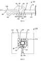
- FIG. 1illustrates a die-up flex BGA package 100 .
- Flex BGA package 100includes an IC die 102 , a tape substrate 104 , a plurality of solder balls 106 , one or more wire bonds 108 , and a stiffener 112 .
- Tape or flex BGA packagesare particularly appropriate for large IC dies with large numbers of input and outputs, such as application specific integrated circuits (ASIC) and microprocessors.
- ASICapplication specific integrated circuits
- Tape substrate 104is generally made from one or more conductive layers bonded with a dielectric material.
- the dielectric materialmay be made from various substances, such as polyimide tape.
- the conductive layersare typically made from a metal, or combination of metals, such as copper and aluminum. Trace or routing patterns are made in the conductive layer material.
- Substrate 104may be a single-layer tape, a two-layer tape, or additional layer tape substrate type. In a two-layer tape, the metal layers sandwich the dielectric layer, such as in a copper-Upilex-copper arrangement. As described above, the IC die is separated from the PCB by the thermal barrier of substrate 104 .
- the plastic substratemay include one or more metal layers formed on an organic substrate (for example, BT resin or FR4 epoxy/glass).
- a stiffenercan be attached to the substrate to add planarity and rigidity to the package, such as stiffener 112 .
- Stiffener 112may be laminated to substrate 104 .
- Stiffener 112is typically made from a metal, or combination of metals, such as copper, tin, and aluminum.
- stiffener 112may be made from a polymer.
- Stiffener 112also may act as a heat sink, and allow for greater heat spreading in BGA package 100 .
- Wire bonds 108connect IC die 102 to substrate 104 .
- Wire bonds 108may be gold, copper, or other types of conductors.
- stiffener 112When stiffener 112 is present, one or more openings 114 in stiffener 112 may be used to allow for wire bonds 108 to connect IC die 102 to substrate 104 .
- Stiffener 112may be configured in other ways, and have different opening arrangements than shown in FIG. 1.
- FIG. 2shows a top view of stiffener 112 .
- Stiffener 112includes an opening 114 adjacent to all four sides of an IC die mounting position 202 in the center of stiffener 112 . Heat transfer from IC die mounting position 202 to the edges of stiffener 112 is substantially limited by openings 114 . Openings 114 act as thermal barriers to heat spreading in stiffener 112 .
- IC die 102is attached to stiffener 112 .
- IC die 102may be attached directly to substrate 104 .
- IC die 102may be attached by an epoxy, for example.
- IC die 102is any type of semiconductor integrated circuit.
- An encapsulant 116which may be an epoxy, mold compound, or other encapsulating material, covers IC die 102 and wire bonds 108 for mechanical and environmental protection.
- wire bondssuch as wire bonds 108
- IC diesmay be mounted and coupled to a substrate with solder balls located on the bottom (active) surface of the IC die, by a process commonly referred to as “C4” or “flip chip” interconnect.
- FIG. 11shows a view of an exemplary solder ball arrangement for a BGA package.
- FIG. 11shows a 14 by 14 array of solder balls 106 on the bottom surface of substrate 104 .
- Other sized arrays of solder ballsare also applicable to the present invention.
- Solder balls 106are reflowed to attach the BGA package to a PCB.
- the PCBmay include contact pads to which solder balls 106 are bonded.
- PCB contact padsare generally made from a metal or combination of metals, such as copper, nickel, tin, and gold.
- the solder ball arraymay be organized in any number of ways, according to the requirements of the particular BGA package application.
- the BGA package substrateprovides vias and routing on one or more layers to connect contact pads for wire bonds on its upper surface to solder balls attached to the bottom substrate surface.
- FIG. 4shows an example routing 404 in a substrate layer 402 for accomplishing this.
- FIG. 3illustrates a die-down BGA package 300 .
- Die-down BGA package 300includes IC die 102 , substrate 104 , plurality of solder balls 106 , one or more wire bonds 108 , and a package stiffener/heat spreader 304 .
- IC die 102is located on the same side of BGA package 300 as are solder balls 106 .
- Substrate 104has a centrally located window shaped opening to accommodate IC die 102 and wire bonds 108 .
- Package stiffener/heat spreader 304mounts IC die 102 , and provides for structural support for BGA package 300 , and aids in the spreading of heat from IC die 102 .
- the configuration of BGA package 300lacks a connection to the PCB from IC die 102 in the center of the package, and hence no direct electrical or thermal path to the PCB exists.
- the present inventionis applicable to improving thermal and electrical performance in the BGA package types described herein, and in other BGA package types.
- the mechanical, electrical, and thermal performances of a BGA packageare enhanced by attaching a heat spreader underneath the BGA package, to a bottom surface of the substrate.
- An IC dieis mounted directly to the heat spreader through a window opening in the substrate, or is mounted to the top surface of the substrate.
- a stiffener or metal ringis also attached to the top surface of the substrate.
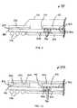
- FIG. 5illustrates a cross-sectional view of a portion of a die-up tape BGA package 500 , according to an embodiment of the present invention.
- BGA package 500includes IC die 102 , substrate 104 , plurality of solder balls 106 , one or more wire bonds 108 , encapsulant 116 , a stiffener or ring 502 , a heat spreader 504 , and one or more ground wire bonds 506 .
- FIG. 6illustrates a top view of die-up tape BGA package 500 (encapsulate 116 not shown).
- One or more wire bonds 108connect corresponding bond pads 118 on IC die 102 to contact points 120 on substrate 104 .
- Substrate 104has a bottom surface to which a top surface of heat spreader 504 is attached by a laminate or adhesive 508 .
- the plurality of solder balls 106are attached to a bottom surface of substrate 104 .
- the plurality of solder balls 106connect to vias and/or points on the bottom surface of substrate 104 to which signals internal to substrate 104 are routed and exposed.
- Substrate 104 in FIG. 5has a central window-shaped opening 512 , which is covered on the bottom surface of substrate 104 by heat spreader 504 .
- FIG. 14shows a top view of substrate 104 with central window-shaped opening 512 .
- Central window shaped opening 506accommodates IC die 102 and wire bonds 506 .
- FIG. 12illustrates a bottom view of a substrate 104 , with heat spreader 504 attached.
- the plurality of solder balls 106are attached to substrate 104 outside an outer dimensional profile of heat spreader 504 .
- a bottom surface of IC die 102is mounted on a top surface of heat spreader 504 using a thermally conductive adhesive 518 or similar substance.
- Adhesive 518may be the same substance as encapsulant 116 , or may be a different substance.
- Silver filled epoxiesmay be used for adhesive 518 to enhance heat extraction from IC die 102 .
- the material used for heat spreader 504may be one or more metals such as copper and aluminum, for example. Heat spreader 504 may be machined, molded, or otherwise manufactured from these materials. Heat spreader 504 may be made from the same material as ring 502 , for example.
- heat spreader 504is configured to operate as a ground plane or power plane.
- one or more power or ground wire bonds 506may be used to connect bond pads 514 on IC die 102 to contact points 516 on heat spreader 504 .
- One or more ground wire bondsmay also be coupled from IC die 102 to a ground ring around the peripheral of IC die 102 .
- the ground ringmay be a silver or palladium plated ground ring.
- the bottom surface of heat spreader 504can be attached to a connection area on a PCB using solder, conductive epoxy, or other substance.
- the PCB connection areais connected to a PCB power or ground plane.
- Such a configurationmay reduce or eliminate power or ground traces on substrate 104 , and reduce the number of solder balls attached to substrate 104 that are dedicated to power or ground. This configuration may also lead to shorter current travel lengths, and may reduce inductance and resistance related to the BGA package. For example, this configuration may enhance electrical performance regarding simultaneous switching noise.
- stiffener or ring 502is attached to the top surface of substrate 104 .
- Ring 502may be attached to substrate 104 by a laminate or adhesive 510 .
- Encapsulant 116is filled in and flushed to ring 502 after the attachment of ring 502 .
- Ring 502is preferably made of a metal, such as copper or aluminum, or a combination thereof, but may also be constructed from other applicable materials.
- ring 502is made from the same material as heat spreader 504 , to minimize the mismatch of the thermal expansion coefficients.
- Ring 502is preferably flush with the outer edges of substrate 104 to form an outer edge of the BGA package, but may also reside entirely within or partially outside an outer profile of substrate 104 .
- a primary benefit of attaching ring 502 to substrate 104is an increase in stiffness of BGA package 500 .
- Ring 502may also aid in reducing the amount of warp of BGA package 500 .
- ring 502promotes heat dissipation from substrate 104 , and may facilitate the attachment of an external heat spreader to BGA package 500 .
- ring 502enhances the process of encapsulation of the BGA package. Ring 502 aids in creating a cavity that may be filled with a dispensed glob top or encapsulating material, such as encapsulant 116 , that locks IC die 102 and surrounding elements in place.
- a dispensed glob top or encapsulating materialsuch as encapsulant 116
- FIG. 12shows a bottom view of a BGA package, with solder balls 106 and heat spreader 504 attached to substrate 104 , according to an embodiment of the present invention.
- An outer dimensional profile 1202 of IC die 102 and an inner dimensional profile 1204 of ring 502are shown, as would be seen through substrate 104 and heat spreader 504 if transparent.
- An outer dimensional profile 1206 of heat spreader 504is also indicated.
- outer profile 1206 of heat spreader 504overlaps with inner profile 1204 of ring 502 . This overlapping portion provides for a low resistance thermal path from IC die 102 to solder balls 106 , including those solder balls 106 at a peripheral of the BGA package, through heat spreader 504 , ring 502 , and substrate 104 .
- viasmay be formed in substrate 104 , in the overlapping area, which may be filled with a conductive material to couple ring 502 to heat spreader 504 , for greater thermal transfer.
- heat spreader 504may be shaped in a variety of ways in addition to the rectangular shape shown in FIG. 12, such as elliptically or irregularly shaped.
- FIG. 7illustrates a cross-sectional view of a portion of a die-up BGA package 700 with heat spreader 504 , according to an alternative embodiment of the present invention.
- FIG. 8shows a top view of die-up BGA package 700 , according to an embodiment of the present invention (encapsulant 116 not shown).
- Die-up BGA package 700is configured substantially similar to BGA package 500 , and the discussion above regarding the elements of BGA package 500 substantially applies to the similar elements of BGA package 700 , subject to the following description.
- IC die 102is mounted to substrate 104 using adhesive 518 or similar substance, instead of being mounted to heat spreader 504 as in BGA package 500 of FIG. 5.
- Substrate 104 of BGA package 700does not include a central window shaped opening as does the substrate of BGA package 500 described above.
- Heat spreader 504is attached to the bottom surface of substrate 104 , and does not directly mount IC die 102 . Heat is transferred through substrate 104 from IC die 102 to heat spreader 504 .
- heat spreader 504aids in dissipating heat produced by IC die 102 by transferring the heat to a PCB to which heat spreader 504 is attached, and/or by transferring heat through substrate 104 to ring 502 .
- Ring 502transfers the heat to a PCB through solder balls 106 , and/or transfers heat to a heat sink coupled to ring 502 directly.
- the mechanical, electrical, and thermal performances of a BGA packageare enhanced by attaching a heat spreader underneath the BGA package, to a bottom surface of the package substrate.
- An IC dieis mounted on a top surface of the substrate, in a flip chip configuration.
- a stiffener or metal ringis also attached to the top surface of the substrate.
- a second heat spreadermay be attached to the IC die and metal ring to further enhance mechanical, electrical, and thermal performances.
- FIG. 9illustrates a cross-sectional view of a portion of a die-up flip chip BGA package 900 with heat spreader 504 , according to an embodiment of the present invention.
- BGA package 900includes IC die 102 , substrate 104 , plurality of solder balls 106 , encapsulant 116 , ring 502 , and heat spreader 504 .
- Die-up flip chip BGA package 900is configured substantially similar to BGA package 700 , and the discussion above regarding the elements of BGA package 700 substantially applies to the similar elements of BGA package 900 , subject to the following description.
- an active surface of IC die 102is attached to substrate 104 with a plurality of conductive bumps 902 , such as solder balls, located on the bottom (active) surface of IC die 102 , by a process commonly referred to as “C4” or “flip chip” packaging.
- the conductive bumps 902couple to conductive pads 904 on the surface of substrate 104 .
- An underfill 908such as an epoxy or encapsulant, may be applied in the gap between IC die 102 and substrate 104 to strengthen their interconnection.
- heat spreader 504aids in dissipating heat produced by IC die 102 by transferring the heat to a PCB to which heat spreader 504 is attached, and/or by transferring heat through substrate 104 to ring 502 .
- thermal and electrical performancemay be enhanced by forming one or more vias 906 in substrate 104 to couple conductive bumps 902 and conductive pads 904 more directly to heat spreader 504 .
- Vias 906may be filled with a conductive material to enhance the thermal and electrical performance of this arrangement. For example, when heat spreader 504 is coupled to a ground or voltage potential of a PCB, vias 906 may be used to provide a short path for the ground or voltage potential of the PCB to IC die 102 .
- FIG. 10illustrates a cross-sectional view of a portion of a die-up flip chip BGA package 1000 with first and second heat spreaders 504 and 1002 , according to an embodiment of the present invention.
- Die-up BGA package 1000is configured substantially similar to BGA package 900 , and the discussion above regarding the elements of BGA package 900 substantially applies to the similar elements of BGA package 1000 , subject to the following description.
- a second heat spreader 1002is attached to a top surface of IC die 102 and a top surface of ring 502 (when present).
- Second heat spreader 1002is attached to ring 502 by an adhesive 1004 , which may be an epoxy, laminate, or similar substance, and is attached to IC die 102 by adhesive 1006 , which may be an epoxy, laminate, or similar substance.
- adhesives 1004 and 1006may be the same substance as encapsulant 116 , the same material as adhesive 518 , or may be a different substance.
- Silver filled epoxiesmay be used for adhesive 1006 to enhance heat extraction from IC die 102 .
- the material used for second heat spreader 1002may be the same as, or different than the material used for heat spreader 504 .
- second heat spreader 1002may be one or more metals such as copper and aluminum, for example.
- Heat spreader 1002may be machined, molded, or otherwise manufactured from these materials.
- Heat spreader 1002may be made from the same material as ring 502 , for example.
- heat spreader 1002may be shaped in a variety of ways.
- Second heat spreader 1002aids in dissipating heat produced by IC die 102 by transferring heat to ring 502 for transfer to a PCB, and by increasing heat dissipation into the environment. Furthermore, second heat spreader 1002 facilitates the connection of additional heat spreaders/heat sinks, such as fin type heat spreaders, to BGA package 1000 . In other words, these additional heat spreaders can be attached to the top of heat spreader 1002 .
- FIG. 13shows a flowchart 1300 providing operational steps for assembling one or more embodiments of the present invention.
- the steps of FIG. 13do not necessarily have to occur in the order shown, as will be apparent to persons skilled in the relevant art(s) based on the teachings herein.
- Other embodimentswill be apparent to persons skilled in the relevant art(s) based on the following discussion. These steps are described in detail below.
- Flowchart 1300begins with step 1302 .
- a substrate that has a first surface and a second surfaceis received.
- the substrateis tape substrate 104 , or another substrate type suitable for a BGA package.
- An IC die mounting position and/or contact pointsmay be provided on a first, upper surface, and solder ball pads may be provided on a second, bottom surface of the substrate.
- a first surface of a heat spreaderis attached to the second substrate surface.
- the heat spreaderis heat spreader 504 , which is attached to substrate 104 .
- a second surface of the heat spreaderis configured to be coupled to a printed circuit board (PCB).
- the second surface of heat spreader 504may be formed as a substantially flat surface to conform to a PCB surface.
- the second heat spreader surfacemay be enabled to be surface mounted to soldering pads on the PCB.
- the second surface of heat spreader 504may be plated with solder or other metals such as nickel, gold, or layers of different metals, to aid in the surface mount process.
- a plurality of solder ballsare attached to the second substrate surface outside an outer dimensional profile of the heat spreader.
- the plurality of solder ballsare plurality of solder balls 106 , which connect to vias and/or solder ball pads on the bottom surface of substrate 104 .
- the solder ballsmay be arranged on the bottom surface of substrate 104 as shown in FIG. 12, or in alternative arrangements.
- the solder ballsare used to attach a BGA package, and signals within, to a PCB.
- Flowchart 1300may include the additional step where a metal ring is attached to the first substrate surface. Attaching the metal ring enhances heat dissipation from the IC die and provides rigidity to the BGA package.
- the metal ringis stiffener or ring 502 .
- step 1304includes the step where a first surface of the heat spreader is attached to the second substrate surface, wherein an outer profile of the heat spreader overlaps with an inner profile of the metal ring.
- a first surface of the heat spreaderis attached to the second substrate surface, wherein an outer profile of the heat spreader overlaps with an inner profile of the metal ring.
- FIGS. 5, 7, 9 , and 10such an arrangement for heat spreader 504 and ring 502 is shown in FIGS. 5, 7, 9 , and 10 .
- portions or all of heat spreader 504 and ring 502do not overlap.
- Flowchart 1300may include the additional step where a window opening is formed in the substrate.
- substrate 104 shown in FIG. 5includes a central window shaped opening 512 . It will be known to persons skilled in the relevant art(s) how to form an opening in a substrate. Such an opening is preferably formed during the substrate manufacturing process.
- Flowchart 1300may include the additional step where an integrated circuit (IC) die is mounted to the first heat spreader surface, wherein the IC die is accessible through the window opening, and may extend at least partially through the window opening.
- IC die 102resides at least partially within window shaped opening 512 .
- the IC diehas a surface that includes at least one contact pad, such as contact pad 118 .
- Flowchart 1300may include the additional step where a wire bond is coupled between one or more of the at least one contact pad and a corresponding metal trace on the first substrate surface.
- wire bond 108is coupled between contact pad 118 and contact point 120 on substrate 104 .
- Contact point 120is a contact point on a metal trace on the surface of substrate 104 .
- the IC diehas a surface that includes at least one ground contact pad, such as ground contact pad 514 .
- Flowchart 1300may include the additional step where a ground wire bond is coupled between at least one ground contact pad and the first heat spreader surface.
- ground wire bond 506is coupled between contact pad 514 and contact point 516 on heat spreader 504 , as shown in FIG. 5.
- Flowchart 1300may include the additional step where the second heat spreader surface is coupled to a ground potential of the PCB.
- heat spreader 504may be coupled to one or more conductive pads on a surface of the PCB that are coupled to PCB ground.
- Flowchart 1300may include the additional step where an integrated circuit (IC) die is mounted to the first substrate surface.
- IC die 102is mounted to substrate 104 , as shown in FIG. 7.
- Flowchart 1300may include the additional step where the IC die is mounted to the first substrate surface in a flip chip configuration.
- IC die 102is mounted to substrate 104 in a flip chip configuration.
- Flowchart 1300may include the additional step where at least one conductive bump on an active surface of the IC die is connected to a corresponding conductive pad on the first substrate surface.
- the plurality of conductive bumps 902are coupled to corresponding conductive pads 904 on substrate 104 .
- Flowchart 1300may include the additional step where a surface of a metal ring is attached to the first substrate surface.
- ring 502is attached to substrate 104 , as shown in FIG. 9.
- step 1304includes the step where a first surface of the heat spreader is attached to the second substrate surface, wherein an outer profile of the heat spreader overlaps with an inner profile of the metal ring.
- a first surface of the heat spreaderis attached to the second substrate surface, wherein an outer profile of the heat spreader overlaps with an inner profile of the metal ring.
- FIGS. 5, 7, 9 , and 10such an arrangement for heat spreader 504 and ring 502 is shown in FIGS. 5, 7, 9 , and 10 .
- portions or all of heat spreader 504 and ring 502do not overlap.
- Flowchart 1300may include the additional step where a second heat spreader is attached to a non-active surface of the IC die and a second surface of the metal ring.
- second heat spreader 1002is attached to IC die 102 and ring 502 (when present) as shown in FIG. 10.
- Flowchart 1300may include the additional step where at least one of the conductive bumps is coupled to the heat spreader through at least one via that extends through the substrate.
- this stepmay include the step where the at least one via is filled with a conductive material.
- these viasare vias 906 shown in FIG. 9.
Landscapes
- Engineering & Computer Science (AREA)
- Computer Hardware Design (AREA)
- Microelectronics & Electronic Packaging (AREA)
- Power Engineering (AREA)
- Physics & Mathematics (AREA)
- Condensed Matter Physics & Semiconductors (AREA)
- General Physics & Mathematics (AREA)
- Chemical & Material Sciences (AREA)
- Materials Engineering (AREA)
- Ceramic Engineering (AREA)
- Cooling Or The Like Of Semiconductors Or Solid State Devices (AREA)
Abstract
Description
- 1. Field of the Invention[0001]
- The invention relates generally to the field of integrated circuit (IC) device packaging technology, and more particularly to heat spreading techniques in ball grid array (BGA) packages.[0002]
- 2. Related Art[0003]
- Integrated circuit (IC) dies are typically mounted in or on a package that is attached to a printed circuit board (PCB). One such type of IC die package is a ball grid array (BGA) package. BGA packages provide for smaller footprints than many other package solutions available today. A BGA package has an array of solder balls located on a bottom external surface of a package substrate. The solder balls are reflowed to attach the package to the PCB. The IC die is mounted to a top surface of the package substrate. Wire bonds typically couple signals in the IC die to the substrate. The substrate has internal routing which electrically couples the IC die signals to the solder balls on the bottom substrate surface.[0004]
- A number of BGA package substrate types exist, including ceramic, plastic, and tape (also known as “flex”). In some BGA package types, a stiffener may be attached to the substrate to supply planarity and rigidity to the package. In such packages, the IC die may be mounted to the stiffener instead of the substrate. Openings in the stiffener may be used to allow the IC die to be wire-bonded to the substrate.[0005]
- Die-up and die-down BGA package configurations exist. In die-up BGA packages, the IC die is mounted on a top surface of the substrate or stiffener, opposite of the side to which the solder balls are attached. In die-down BGA packages, the IC die is mounted on a bottom surface of the substrate or stiffener, on the same side as which the solder balls are attached.[0006]
- Conventional BGA packages are subject to high thermal stresses that result from the heat given off during operation of the mounted IC die. The thermal stresses are primarily imposed on the IC die and solder balls due to the mismatch of the thermal expansion coefficient (CTE) between the semiconductor die and the metal stiffener. As a result, conventional flex BGA packages have difficulty in meeting reliability requirements for die sizes larger than 9 mm. See, e.g., Thompson, T., et al.,[0007]Reliability Assessment of a Thin(Flex)BGA Using a Polyimide Tape Substrate, International Electronics Manufacturing Technology Symposium, IEEE, pp. 207-213 (1999).
- The tape substrate used in flex BGA packages is typically polyimide, which has very low values of thermal conductivity. Consequently, the IC die is separated from the PCB by the tape substrate thermal barrier. The lack of direct thermal connection from IC die to PCB leads to relatively high resistance to heat transfer from IC die-to-board (theta-jb).[0008]
- A stiffener attached to a substrate enhances heat spreading. However, the openings on the stiffener for wire bond connections tend to reduce the thermal connections between the IC die and the edges of the stiffener. As a result, heat spreading is limited largely to the region of the IC die attach pad, while areas at the stiffener peripheral do not contribute effectively to heat spreading.[0009]
- Furthermore, because of the high density of the substrate routing circuitry, it is difficult to bond each power and ground pad on the IC die to the substrate by a corresponding bond finger. As a result, the distribution of ground and power signals connecting to the IC die is frequently compromised in conventional BGA packages.[0010]
- Ball grid array packages that use plastic substrates (for example, BT or FR4 plastic) are commonly known as plastic BGAs, or PBGAs. See, e.g., Lau, J. H.,[0011]Ball Grid Array Technology, McGraw-Hill, New York, (1995). A PBGA package, for example, may add solder balls to the bottom substrate surface under the IC die to aid in conducting heat to the PCB. Solder balls such as these are referred to as thermal balls. The cost of the PBGA package, however, will increase with the number of thermal balls. Furthermore, a large array of thermal balls may be necessary for heat dissipation into the PCB for high levels of IC device power.
- Hence, what is needed are BGA packages with improved heat spreading capabilities, while also providing for high levels of IC electrical performance.[0012]
- The present invention is directed at ball grid array (BGA)packages having enhanced electrical and thermal characteristics. In one aspect, a substrate has a first surface and a second surface. A heat spreader has a first surface and a second surface. The first heat spreader surface is attached to the second substrate surface. A plurality of solder balls are attached to the second substrate surface outside an outer dimensional profile of the heat spreader. The second heat spreader surface is configured to be coupled to a printed circuit board (PCB).[0013]
- In a further aspect, a metal ring is attached to the first substrate surface. An outer profile of said heat spreader overlaps with an inner profile of the metal ring.[0014]
- In a still further aspect, the substrate has a window opening. An integrated circuit (IC) die is mounted to the first heat spreader surface and is accessible through the window opening. The IC die has a surface that includes at least one contact pad. A wire bond corresponding to each contact pad couples the contact pad to a corresponding metal trace on the first substrate surface. The IC die has a surface that includes at least one ground contact pad. A ground wire bond corresponding to each ground contact pad couples the ground contact pad to the first heat spreader surface. The second heat spreader surface is coupled to a ground potential of the PCB.[0015]
- In an alternative aspect, an IC die is mounted to the first substrate surface. The IC die is mounted to the first substrate surface in a flip chip configuration. At least one conductive bump on an active surface of the IC die is connected to a corresponding conductive pad on the first substrate surface. A second heat spreader is attached to a non-active surface of said IC die.[0016]
- In a further aspect, at least one via extends through the substrate. Each via is filled with a conductive material to couple one of the conductive bumps to the first heat spreader.[0017]
- Further aspects of the present invention, and further features and benefits thereof, are described below. The accompanying drawings, which are incorporated herein and form a part of the specification, illustrate the present invention and, together with the description, further serve to explain the principles of the invention and to enable a person skilled in the pertinent art to make and use the invention.[0018]
- The accompanying drawings, which are incorporated herein and form a part of the specification, illustrate the present invention and, together with the description, further serve to explain the principles of the invention and to enable a person skilled in the pertinent art to make and use the invention.[0019]
- FIG. 1 illustrates a cross-sectional view of a die-up BGA package.[0020]
- FIG. 2 illustrates a top view of a stiffener.[0021]
- FIG. 3 illustrates a cross-sectional view of a die-down BGA package.[0022]
- FIG. 4 shows exemplary routing in a substrate layer.[0023]
- FIG. 5 illustrates a cross-sectional view of a portion of a die-up BGA package with heat spreader, according to an embodiment of the present invention.[0024]
- FIG. 6 shows atop view of the die-up BGA package of FIG. 5, according to an embodiment of the present invention.[0025]
- FIG. 7 illustrates a cross-sectional view of a portion of a die-up BGA package with heat spreader, according to an embodiment of the present invention.[0026]
- FIG. 8 shows a top view of the die-up BGA package of FIG. 7, according to an embodiment of the present invention.[0027]
- FIG. 9 illustrates a cross-sectional view of a portion of a die-up flip chip BGA package with heat spreader, according to an embodiment of the present invention.[0028]
- FIG. 10 illustrates a cross-sectional view of a portion of a die-up flip chip BGA package with two heat spreaders, according to an embodiment of the present invention.[0029]
- FIG. 11 shows a view of an exemplary solder ball arrangement for a BGA package.[0030]
- FIG. 12 illustrates solder balls and a heat spreader attached to a substrate, according to an embodiment of the present invention.[0031]
- FIG. 13 shows a flowchart that provides operational steps of exemplary embodiments of the present invention.[0032]
- FIG. 14 shows a top view of a substrate with a central window-shaped opening.[0033]
- The present invention will now be described with reference to the accompanying drawings. In the drawings, like reference numbers indicate identical or functionally similar elements. Additionally, the left-most digit(s) of a reference number identifies the drawing in which the reference number first appears.[0034]
- Overview[0035]
- The present invention is directed to a method and system for improving the mechanical, thermal, and electrical performance of BGA packages. The present invention is applicable to all types of BGA substrates, including ceramic, plastic, and tape (flex) BGA packages. Furthermore the present invention is applicable to die-up (cavity-up) and die-down (cavity-down) orientations.[0036]
- Numerous embodiments of the present invention are presented herein. In a first embodiment, the BGA package IC die is mounted to a heat spreader. In a second embodiment, a heat spreader is attached to a first side of a BGA package substrate, and the IC die is mounted to a second side of the substrate. In a third embodiment, a heat spreader is again mounted to the first side of the substrate, and the IC die is mounted to the second side of the substrate in a flip chip configuration. In a fourth embodiment, a heat spreader is again mounted to the first side of the substrate, and the IC die is mounted to the second side of the substrate in a flip chip configuration. Furthermore, a second heat spreader is mounted to a top surface of the IC die. In each embodiment, BGA package thermal dissipation and electrical performance are improved. In each embodiment, the first heat spreader may be coupled to a printed circuit board (PCB) to further improve thermal and electrical performance. The embodiments of the present invention presented herein allow large size dies with high input and output (I/O) counts to be packaged using BGA technology. For example, additional I/O counts may be gained due to the elimination or reduction in ground solder balls by the present invention.[0037]
- Ball grid array package types are described below. Further detail on the above described embodiments, and additional embodiments according to the present invention, are presented below. The embodiments described herein may be combined in any applicable manner, as required by a particular application.[0038]
- Ball Grid Array (BGA) Packages[0039]
- A ball grid array (BGA) package is used to package and interface an IC die with a printed circuit board (PCB). BGA packages may be used with any type of IC die, and are particularly useful for high speed ICs. In a BGA package, solder pads do not just surround the package periphery, as in chip carrier type packages, but partially or entirely cover the bottom package surface in an array configuration. BGA packages are also referred to as pad array carrier (PAC), pad array, land grid array, and pad-grid array packages. BGA packages types are further described in the following paragraphs. For additional description on BGA packages, refer to Lau, J. H.,[0040]Ball Grid Array Technology, McGraw-Hill, New York, (1995), which is herein incorporated by reference in its entirety.
- Die-up and die-down BGA package configurations exist. In die-up BGA packages, the IC die is mounted on a top surface of the substrate or stiffener, in a direction away from the PCB. In die-down BGA packages, the IC die is mounted on a bottom surface of the substrate or stiffener, in a direction towards the PCB.[0041]
- A number of BGA package substrate types exist, including ceramic, plastic (PBGA), and tape (also known as “flex”). FIG. 1 illustrates a die-up[0042]
flex BGA package 100.Flex BGA package 100 includes anIC die 102, atape substrate 104, a plurality ofsolder balls 106, one ormore wire bonds 108, and astiffener 112. Tape or flex BGA packages are particularly appropriate for large IC dies with large numbers of input and outputs, such as application specific integrated circuits (ASIC) and microprocessors. - [0043]
Tape substrate 104 is generally made from one or more conductive layers bonded with a dielectric material. For instance, the dielectric material may be made from various substances, such as polyimide tape. The conductive layers are typically made from a metal, or combination of metals, such as copper and aluminum. Trace or routing patterns are made in the conductive layer material.Substrate 104 may be a single-layer tape, a two-layer tape, or additional layer tape substrate type. In a two-layer tape, the metal layers sandwich the dielectric layer, such as in a copper-Upilex-copper arrangement. As described above, the IC die is separated from the PCB by the thermal barrier ofsubstrate 104. In a plastic substrate embodiment, the plastic substrate may include one or more metal layers formed on an organic substrate (for example, BT resin or FR4 epoxy/glass). - In some BGA package types, particularly in flex BGA packages, a stiffener can be attached to the substrate to add planarity and rigidity to the package, such as[0044]
stiffener 112.Stiffener 112 may be laminated tosubstrate 104.Stiffener 112 is typically made from a metal, or combination of metals, such as copper, tin, and aluminum. Alternatively,stiffener 112 may be made from a polymer.Stiffener 112 also may act as a heat sink, and allow for greater heat spreading inBGA package 100. - One or[0045]
more wire bonds 108 connect IC die102 tosubstrate 104.Wire bonds 108 may be gold, copper, or other types of conductors. Whenstiffener 112 is present, one ormore openings 114 instiffener 112 may be used to allow forwire bonds 108 to connect IC die102 tosubstrate 104.Stiffener 112 may be configured in other ways, and have different opening arrangements than shown in FIG. 1. - The use of a stiffener in a flex BGA package requires additional considerations when attempting to manage heat spreading. FIG. 2 shows a top view of[0046]
stiffener 112.Stiffener 112 includes anopening 114 adjacent to all four sides of an ICdie mounting position 202 in the center ofstiffener 112. Heat transfer from IC die mountingposition 202 to the edges ofstiffener 112 is substantially limited byopenings 114.Openings 114 act as thermal barriers to heat spreading instiffener 112. - IC die[0047]102 is attached to
stiffener 112. In alternative configurations, when a stiffener is not present, IC die102 may be attached directly tosubstrate 104. IC die102 may be attached by an epoxy, for example. IC die102 is any type of semiconductor integrated circuit. - An[0048]
encapsulant 116, which may be an epoxy, mold compound, or other encapsulating material, covers IC die102 andwire bonds 108 for mechanical and environmental protection. - Note that although wire bonds, such as[0049]
wire bonds 108, are shown and described herein, IC dies may be mounted and coupled to a substrate with solder balls located on the bottom (active) surface of the IC die, by a process commonly referred to as “C4” or “flip chip” interconnect. - FIG. 11 shows a view of an exemplary solder ball arrangement for a BGA package. FIG. 11 shows a 14 by 14 array of[0050]
solder balls 106 on the bottom surface ofsubstrate 104. Other sized arrays of solder balls are also applicable to the present invention.Solder balls 106 are reflowed to attach the BGA package to a PCB. The PCB may include contact pads to whichsolder balls 106 are bonded. PCB contact pads are generally made from a metal or combination of metals, such as copper, nickel, tin, and gold. The solder ball array may be organized in any number of ways, according to the requirements of the particular BGA package application. - As described above, the BGA package substrate provides vias and routing on one or more layers to connect contact pads for wire bonds on its upper surface to solder balls attached to the bottom substrate surface. FIG. 4 shows an[0051]
example routing 404 in asubstrate layer 402 for accomplishing this. - FIG. 3 illustrates a die-[0052]
down BGA package 300. Die-down BGA package 300 includes IC die102,substrate 104, plurality ofsolder balls 106, one ormore wire bonds 108, and a package stiffener/heat spreader 304. As shown in FIG. 3, IC die102 is located on the same side ofBGA package 300 as aresolder balls 106.Substrate 104 has a centrally located window shaped opening to accommodate IC die102 andwire bonds 108. Package stiffener/heat spreader 304 mounts IC die102, and provides for structural support forBGA package 300, and aids in the spreading of heat from IC die102. The configuration ofBGA package 300 lacks a connection to the PCB from IC die102 in the center of the package, and hence no direct electrical or thermal path to the PCB exists. - The present invention is applicable to improving thermal and electrical performance in the BGA package types described herein, and in other BGA package types.[0053]
- BGA Embodiments According to the Present Invention[0054]
- Further details of structural and operational implementations of ball grid array packages of the present invention are described in the following sections. These structural and operational implementations are described herein for illustrative purposes, and are not limiting. For instance, the present invention as described herein may be implemented in both die-up and die-down BGA package types, as well as other IC package types. Furthermore, each of the embodiments presented below are applicable to tape substrate BGA packages, plastic substrate BGA packages, and ceramic substrate BGA packages. The description below is adaptable to these and other package types, as would be understood to persons skilled in the relevant art(s) from the teachings herein. For instance, in some tape BGA packages, a stiffener may be required in the BGA package.[0055]
- Features of each of the embodiments presented below may be incorporated into BGA packages independently, or may be combined in any manner, as would be apparent to persons skilled in the relevant art(s) from the teachings herein.[0056]
- Wire Bonded IC Die Embodiments[0057]
- According to embodiments of the present invention, the mechanical, electrical, and thermal performances of a BGA package are enhanced by attaching a heat spreader underneath the BGA package, to a bottom surface of the substrate. An IC die is mounted directly to the heat spreader through a window opening in the substrate, or is mounted to the top surface of the substrate. Furthermore, in a preferred embodiment, a stiffener or metal ring is also attached to the top surface of the substrate.[0058]
- FIG. 5 illustrates a cross-sectional view of a portion of a die-up[0059]
tape BGA package 500, according to an embodiment of the present invention.BGA package 500 includes IC die102,substrate 104, plurality ofsolder balls 106, one ormore wire bonds 108,encapsulant 116, a stiffener orring 502, aheat spreader 504, and one or more ground wire bonds506. FIG. 6 illustrates a top view of die-up tape BGA package500 (encapsulate116 not shown). - One or[0060]
more wire bonds 108 connect correspondingbond pads 118 on IC die102 to contactpoints 120 onsubstrate 104. - [0061]
Substrate 104 has a bottom surface to which a top surface ofheat spreader 504 is attached by a laminate or adhesive508. The plurality ofsolder balls 106 are attached to a bottom surface ofsubstrate 104. The plurality ofsolder balls 106 connect to vias and/or points on the bottom surface ofsubstrate 104 to which signals internal tosubstrate 104 are routed and exposed.Substrate 104 in FIG. 5 has a central window-shapedopening 512, which is covered on the bottom surface ofsubstrate 104 byheat spreader 504. FIG. 14 shows a top view ofsubstrate 104 with central window-shapedopening 512. Central window shapedopening 506 accommodates IC die102 andwire bonds 506. FIG. 12 illustrates a bottom view of asubstrate 104, withheat spreader 504 attached. The plurality ofsolder balls 106 are attached tosubstrate 104 outside an outer dimensional profile ofheat spreader 504. - As shown in FIG. 5, a bottom surface of IC die[0062]102 is mounted on a top surface of
heat spreader 504 using a thermally conductive adhesive518 or similar substance. Adhesive518 may be the same substance asencapsulant 116, or may be a different substance. Silver filled epoxies may be used for adhesive518 to enhance heat extraction from IC die102. By configuringheat spreader 504 between IC die102 and the PCB, a direct thermal path is formed between the IC die102 and PCB, improving thermal performance. - The material used for[0063]
heat spreader 504 may be one or more metals such as copper and aluminum, for example.Heat spreader 504 may be machined, molded, or otherwise manufactured from these materials.Heat spreader 504 may be made from the same material asring 502, for example. - In an embodiment,[0064]
heat spreader 504 is configured to operate as a ground plane or power plane. For example, one or more power orground wire bonds 506 may be used to connectbond pads 514 on IC die102 to contactpoints 516 onheat spreader 504. One or more ground wire bonds may also be coupled from IC die102 to a ground ring around the peripheral of IC die102. For example, the ground ring may be a silver or palladium plated ground ring. The bottom surface ofheat spreader 504 can be attached to a connection area on a PCB using solder, conductive epoxy, or other substance. The PCB connection area is connected to a PCB power or ground plane. Such a configuration may reduce or eliminate power or ground traces onsubstrate 104, and reduce the number of solder balls attached tosubstrate 104 that are dedicated to power or ground. This configuration may also lead to shorter current travel lengths, and may reduce inductance and resistance related to the BGA package. For example, this configuration may enhance electrical performance regarding simultaneous switching noise. - In an embodiment, stiffener or[0065]
ring 502 is attached to the top surface ofsubstrate 104.Ring 502 may be attached tosubstrate 104 by a laminate or adhesive510.Encapsulant 116 is filled in and flushed to ring502 after the attachment ofring 502.Ring 502 is preferably made of a metal, such as copper or aluminum, or a combination thereof, but may also be constructed from other applicable materials. Preferably,ring 502 is made from the same material asheat spreader 504, to minimize the mismatch of the thermal expansion coefficients.Ring 502 is preferably flush with the outer edges ofsubstrate 104 to form an outer edge of the BGA package, but may also reside entirely within or partially outside an outer profile ofsubstrate 104. - A primary benefit of attaching[0066]
ring 502 tosubstrate 104 is an increase in stiffness ofBGA package 500.Ring 502 may also aid in reducing the amount of warp ofBGA package 500. Furthermore,ring 502 promotes heat dissipation fromsubstrate 104, and may facilitate the attachment of an external heat spreader toBGA package 500. - Furthermore,[0067]
ring 502 enhances the process of encapsulation of the BGA package.Ring 502 aids in creating a cavity that may be filled with a dispensed glob top or encapsulating material, such asencapsulant 116, that locks IC die102 and surrounding elements in place. - As described above, FIG. 12 shows a bottom view of a BGA package, with[0068]
solder balls 106 andheat spreader 504 attached tosubstrate 104, according to an embodiment of the present invention. An outerdimensional profile 1202 of IC die102 and an innerdimensional profile 1204 ofring 502 are shown, as would be seen throughsubstrate 104 andheat spreader 504 if transparent. An outerdimensional profile 1206 ofheat spreader 504 is also indicated. In a preferred embodiment, as shown in FIG. 12,outer profile 1206 ofheat spreader 504 overlaps withinner profile 1204 ofring 502. This overlapping portion provides for a low resistance thermal path from IC die102 tosolder balls 106, including thosesolder balls 106 at a peripheral of the BGA package, throughheat spreader 504,ring 502, andsubstrate 104. - Note that vias may be formed in[0069]
substrate 104, in the overlapping area, which may be filled with a conductive material tocouple ring 502 to heatspreader 504, for greater thermal transfer. Furthermore, note thatheat spreader 504 may be shaped in a variety of ways in addition to the rectangular shape shown in FIG. 12, such as elliptically or irregularly shaped. - FIG. 7 illustrates a cross-sectional view of a portion of a die-up[0070]
BGA package 700 withheat spreader 504, according to an alternative embodiment of the present invention. FIG. 8 shows a top view of die-upBGA package 700, according to an embodiment of the present invention (encapsulant 116 not shown). Die-up BGA package 700 is configured substantially similar toBGA package 500, and the discussion above regarding the elements ofBGA package 500 substantially applies to the similar elements ofBGA package 700, subject to the following description. - In the embodiment of[0071]
BGA package 700 shown in FIGS. 7 and 8, IC die102 is mounted tosubstrate 104 using adhesive518 or similar substance, instead of being mounted toheat spreader 504 as inBGA package 500 of FIG. 5.Substrate 104 ofBGA package 700 does not include a central window shaped opening as does the substrate ofBGA package 500 described above.Heat spreader 504 is attached to the bottom surface ofsubstrate 104, and does not directly mount IC die102. Heat is transferred throughsubstrate 104 from IC die102 to heatspreader 504. As described above,heat spreader 504 aids in dissipating heat produced by IC die102 by transferring the heat to a PCB to whichheat spreader 504 is attached, and/or by transferring heat throughsubstrate 104 toring 502.Ring 502 transfers the heat to a PCB throughsolder balls 106, and/or transfers heat to a heat sink coupled to ring502 directly. - The embodiments provided above in this section are presented herein for purposes of illustration, and not limitation. The invention is not limited to the particular examples of components and methods described herein. Alternatives (including equivalents, extensions, variations, deviations, etc., of those described herein) will be apparent to persons skilled in the relevant art(s) based on the teachings contained herein. Such alternatives fall within the scope and spirit of the present invention.[0072]
- Flip Chip IC Die Embodiments[0073]
- According to embodiments of the present invention, the mechanical, electrical, and thermal performances of a BGA package are enhanced by attaching a heat spreader underneath the BGA package, to a bottom surface of the package substrate. An IC die is mounted on a top surface of the substrate, in a flip chip configuration. In a preferred embodiment, a stiffener or metal ring is also attached to the top surface of the substrate. Furthermore, a second heat spreader may be attached to the IC die and metal ring to further enhance mechanical, electrical, and thermal performances.[0074]
- FIG. 9 illustrates a cross-sectional view of a portion of a die-up flip[0075]
chip BGA package 900 withheat spreader 504, according to an embodiment of the present invention.BGA package 900 includes IC die102,substrate 104, plurality ofsolder balls 106,encapsulant 116,ring 502, andheat spreader 504. Die-up flipchip BGA package 900 is configured substantially similar toBGA package 700, and the discussion above regarding the elements ofBGA package 700 substantially applies to the similar elements ofBGA package 900, subject to the following description. - In the embodiment of[0076]
BGA package 900 shown in FIG. 9, an active surface of IC die102 is attached tosubstrate 104 with a plurality ofconductive bumps 902, such as solder balls, located on the bottom (active) surface of IC die102, by a process commonly referred to as “C4” or “flip chip” packaging. Theconductive bumps 902 couple toconductive pads 904 on the surface ofsubstrate 104. - An[0077]
underfill 908, such as an epoxy or encapsulant, may be applied in the gap between IC die102 andsubstrate 104 to strengthen their interconnection. - As described above,[0078]
heat spreader 504 aids in dissipating heat produced by IC die102 by transferring the heat to a PCB to whichheat spreader 504 is attached, and/or by transferring heat throughsubstrate 104 toring 502. In an embodiment, thermal and electrical performance may be enhanced by forming one ormore vias 906 insubstrate 104 to coupleconductive bumps 902 andconductive pads 904 more directly toheat spreader 504.Vias 906 may be filled with a conductive material to enhance the thermal and electrical performance of this arrangement. For example, whenheat spreader 504 is coupled to a ground or voltage potential of a PCB, vias906 may be used to provide a short path for the ground or voltage potential of the PCB to IC die102. - FIG. 10 illustrates a cross-sectional view of a portion of a die-up flip[0079]
chip BGA package 1000 with first andsecond heat spreaders up BGA package 1000 is configured substantially similar toBGA package 900, and the discussion above regarding the elements ofBGA package 900 substantially applies to the similar elements ofBGA package 1000, subject to the following description. - In the embodiment of[0080]
BGA package 1000 shown in FIG. 10, asecond heat spreader 1002 is attached to a top surface of IC die102 and a top surface of ring502 (when present).Second heat spreader 1002 is attached to ring502 by an adhesive1004, which may be an epoxy, laminate, or similar substance, and is attached to IC die102 by adhesive1006, which may be an epoxy, laminate, or similar substance. For example,adhesives encapsulant 116, the same material as adhesive518, or may be a different substance. Silver filled epoxies may be used for adhesive1006 to enhance heat extraction from IC die102. - The material used for[0081]
second heat spreader 1002 may be the same as, or different than the material used forheat spreader 504. For example,second heat spreader 1002 may be one or more metals such as copper and aluminum, for example.Heat spreader 1002 may be machined, molded, or otherwise manufactured from these materials.Heat spreader 1002 may be made from the same material asring 502, for example. Furthermore,heat spreader 1002 may be shaped in a variety of ways. - [0082]
Second heat spreader 1002 aids in dissipating heat produced by IC die102 by transferring heat to ring502 for transfer to a PCB, and by increasing heat dissipation into the environment. Furthermore,second heat spreader 1002 facilitates the connection of additional heat spreaders/heat sinks, such as fin type heat spreaders, toBGA package 1000. In other words, these additional heat spreaders can be attached to the top ofheat spreader 1002. - The embodiments provided above in this section are presented herein for purposes of illustration, and not limitation. The invention is not limited to the particular examples of components and methods described herein. Alternatives (including equivalents, extensions, variations, deviations, etc., of those described herein) will be apparent to persons skilled in the relevant art(s) based on the teachings contained herein. Such alternatives fall within the scope and spirit of the present invention.[0083]
- Assembling Ball Grid Array Packages According to Embodiments of the Present Invention[0084]
- FIG. 13 shows a[0085]
flowchart 1300 providing operational steps for assembling one or more embodiments of the present invention. The steps of FIG. 13 do not necessarily have to occur in the order shown, as will be apparent to persons skilled in the relevant art(s) based on the teachings herein. Other embodiments will be apparent to persons skilled in the relevant art(s) based on the following discussion. These steps are described in detail below. - [0086]
Flowchart 1300 begins withstep 1302.Instep 1302, a substrate that has a first surface and a second surface is received. For example, the substrate istape substrate 104, or another substrate type suitable for a BGA package. An IC die mounting position and/or contact points may be provided on a first, upper surface, and solder ball pads may be provided on a second, bottom surface of the substrate. - In[0087]
step 1304, a first surface of a heat spreader is attached to the second substrate surface. For example, the heat spreader isheat spreader 504, which is attached tosubstrate 104. - In[0088]
step 1306, a second surface of the heat spreader is configured to be coupled to a printed circuit board (PCB). For example, the second surface ofheat spreader 504 may be formed as a substantially flat surface to conform to a PCB surface. The second heat spreader surface may be enabled to be surface mounted to soldering pads on the PCB. For example, the second surface ofheat spreader 504 may be plated with solder or other metals such as nickel, gold, or layers of different metals, to aid in the surface mount process. - In[0089]
step 1308, a plurality of solder balls are attached to the second substrate surface outside an outer dimensional profile of the heat spreader. For example, the plurality of solder balls are plurality ofsolder balls 106, which connect to vias and/or solder ball pads on the bottom surface ofsubstrate 104. The solder balls may be arranged on the bottom surface ofsubstrate 104 as shown in FIG. 12, or in alternative arrangements. The solder balls are used to attach a BGA package, and signals within, to a PCB. - [0090]
Flowchart 1300 may include the additional step where a metal ring is attached to the first substrate surface. Attaching the metal ring enhances heat dissipation from the IC die and provides rigidity to the BGA package. For example, the metal ring is stiffener orring 502. - In an embodiment,[0091]
step 1304 includes the step where a first surface of the heat spreader is attached to the second substrate surface, wherein an outer profile of the heat spreader overlaps with an inner profile of the metal ring. For example, such an arrangement forheat spreader 504 andring 502 is shown in FIGS. 5, 7,9, and10. In alternative embodiments, portions or all ofheat spreader 504 andring 502 do not overlap. - [0092]
Flowchart 1300 may include the additional step where a window opening is formed in the substrate. For example,substrate 104 shown in FIG. 5 includes a central window shapedopening 512. It will be known to persons skilled in the relevant art(s) how to form an opening in a substrate. Such an opening is preferably formed during the substrate manufacturing process. - [0093]
Flowchart 1300 may include the additional step where an integrated circuit (IC) die is mounted to the first heat spreader surface, wherein the IC die is accessible through the window opening, and may extend at least partially through the window opening. For example, as shown in FIG. 5, IC die102 resides at least partially within window shapedopening 512. - In an embodiment, the IC die has a surface that includes at least one contact pad, such as[0094]
contact pad 118.Flowchart 1300 may include the additional step where a wire bond is coupled between one or more of the at least one contact pad and a corresponding metal trace on the first substrate surface. For example,wire bond 108 is coupled betweencontact pad 118 andcontact point 120 onsubstrate 104.Contact point 120 is a contact point on a metal trace on the surface ofsubstrate 104. - In an embodiment, the IC die has a surface that includes at least one ground contact pad, such as[0095]
ground contact pad 514.Flowchart 1300 may include the additional step where a ground wire bond is coupled between at least one ground contact pad and the first heat spreader surface. For example,ground wire bond 506 is coupled betweencontact pad 514 andcontact point 516 onheat spreader 504, as shown in FIG. 5. - [0096]
Flowchart 1300 may include the additional step where the second heat spreader surface is coupled to a ground potential of the PCB. For example,heat spreader 504 may be coupled to one or more conductive pads on a surface of the PCB that are coupled to PCB ground. - [0097]
Flowchart 1300 may include the additional step where an integrated circuit (IC) die is mounted to the first substrate surface. For example, IC die102 is mounted tosubstrate 104, as shown in FIG. 7. - [0098]
Flowchart 1300 may include the additional step where the IC die is mounted to the first substrate surface in a flip chip configuration. For example, as shown in FIG. 9, IC die102 is mounted tosubstrate 104 in a flip chip configuration. - [0099]
Flowchart 1300 may include the additional step where at least one conductive bump on an active surface of the IC die is connected to a corresponding conductive pad on the first substrate surface. For example, the plurality ofconductive bumps 902 are coupled to correspondingconductive pads 904 onsubstrate 104. - [0100]
Flowchart 1300 may include the additional step where a surface of a metal ring is attached to the first substrate surface. For example,ring 502 is attached tosubstrate 104, as shown in FIG. 9. - In an embodiment,[0101]
step 1304 includes the step where a first surface of the heat spreader is attached to the second substrate surface, wherein an outer profile of the heat spreader overlaps with an inner profile of the metal ring. For example, such an arrangement forheat spreader 504 andring 502 is shown in FIGS. 5, 7,9, and10. In alternative embodiments, portions or all ofheat spreader 504 andring 502 do not overlap. - [0102]
Flowchart 1300 may include the additional step where a second heat spreader is attached to a non-active surface of the IC die and a second surface of the metal ring. For example,second heat spreader 1002 is attached to IC die102 and ring502 (when present) as shown in FIG. 10. - [0103]
Flowchart 1300 may include the additional step where at least one of the conductive bumps is coupled to the heat spreader through at least one via that extends through the substrate. In an embodiment, this step may include the step where the at least one via is filled with a conductive material. For example, these vias are vias906 shown in FIG. 9. - Conclusion[0104]
- While various embodiments of the present invention have been described above, it should be understood that they have been presented by way of example only, and not limitation. It will be apparent to persons skilled in the relevant art that various changes in form and detail can be made therein without departing from the spirit and scope of the invention. Thus, the breadth and scope of the present invention should not be limited by any of the above-described exemplary embodiments, but should be defined only in accordance with the following claims and their equivalents.[0105]
Claims (37)
Priority Applications (6)
| Application Number | Priority Date | Filing Date | Title |
|---|---|---|---|
| US09/849,537US7259448B2 (en) | 2001-05-07 | 2001-05-07 | Die-up ball grid array package with a heat spreader and method for making the same |
| TW091108573ATWI282154B (en) | 2001-05-07 | 2002-04-25 | Die-up ball grid array package with a heat spreader and method for making the same |
| EP02252969AEP1256980B1 (en) | 2001-05-07 | 2002-04-26 | Ball grid array package with a heat spreader and method for making the same |
| AT02252969TATE521086T1 (en) | 2001-05-07 | 2002-04-26 | BALL MATRIX HOUSING WITH HEAT DISTRIBUTOR AND ITS PRODUCTION |
| US10/939,075US7259457B2 (en) | 2001-05-07 | 2004-09-13 | Die-up ball grid array package including a substrate capable of mounting an integrated circuit die and method for making the same |
| US10/938,955US20050035452A1 (en) | 2001-05-07 | 2004-09-13 | Die-up ball grid array package including a substrate having an opening and method for making the same |
Applications Claiming Priority (1)
| Application Number | Priority Date | Filing Date | Title |
|---|---|---|---|
| US09/849,537US7259448B2 (en) | 2001-05-07 | 2001-05-07 | Die-up ball grid array package with a heat spreader and method for making the same |
Related Child Applications (2)
| Application Number | Title | Priority Date | Filing Date |
|---|---|---|---|
| US10/938,955DivisionUS20050035452A1 (en) | 2001-05-07 | 2004-09-13 | Die-up ball grid array package including a substrate having an opening and method for making the same |
| US10/939,075DivisionUS7259457B2 (en) | 2001-05-07 | 2004-09-13 | Die-up ball grid array package including a substrate capable of mounting an integrated circuit die and method for making the same |
Publications (2)
| Publication Number | Publication Date |
|---|---|
| US20020171144A1true US20020171144A1 (en) | 2002-11-21 |
| US7259448B2 US7259448B2 (en) | 2007-08-21 |
Family
ID=25305948
Family Applications (3)
| Application Number | Title | Priority Date | Filing Date |
|---|---|---|---|
| US09/849,537Expired - LifetimeUS7259448B2 (en) | 2001-05-07 | 2001-05-07 | Die-up ball grid array package with a heat spreader and method for making the same |
| US10/938,955AbandonedUS20050035452A1 (en) | 2001-05-07 | 2004-09-13 | Die-up ball grid array package including a substrate having an opening and method for making the same |
| US10/939,075Expired - LifetimeUS7259457B2 (en) | 2001-05-07 | 2004-09-13 | Die-up ball grid array package including a substrate capable of mounting an integrated circuit die and method for making the same |
Family Applications After (2)
| Application Number | Title | Priority Date | Filing Date |
|---|---|---|---|
| US10/938,955AbandonedUS20050035452A1 (en) | 2001-05-07 | 2004-09-13 | Die-up ball grid array package including a substrate having an opening and method for making the same |
| US10/939,075Expired - LifetimeUS7259457B2 (en) | 2001-05-07 | 2004-09-13 | Die-up ball grid array package including a substrate capable of mounting an integrated circuit die and method for making the same |
Country Status (4)
| Country | Link |
|---|---|
| US (3) | US7259448B2 (en) |
| EP (1) | EP1256980B1 (en) |
| AT (1) | ATE521086T1 (en) |
| TW (1) | TWI282154B (en) |
Cited By (40)
| Publication number | Priority date | Publication date | Assignee | Title |
|---|---|---|---|---|
| US20020185734A1 (en)* | 2000-12-22 | 2002-12-12 | Zhao Sam Ziqun | Die-up ball grid array package with printed circuit board attachable heat spreader |
| US20030057550A1 (en)* | 2000-12-22 | 2003-03-27 | Broadcom Corporation | Ball grid array package enhanced with a thermal and electrical connector |
| US20030111726A1 (en)* | 2001-12-18 | 2003-06-19 | Khan Reza-Ur Rahman | Ball grid array package substrates and method of making the same |
| US20030146506A1 (en)* | 2002-02-01 | 2003-08-07 | Broadcom Corporation | Ball grid array package fabrication with IC die support structures |
| US20030146511A1 (en)* | 2002-02-01 | 2003-08-07 | Broadcom Corporation | Ball grid array package with multiple interposers |
| US20030146509A1 (en)* | 2002-02-01 | 2003-08-07 | Broadcom Corporation | Ball grid array package with separated stiffener layer |
| US20030179556A1 (en)* | 2002-03-21 | 2003-09-25 | Broadcom Corporation | Enhanced die-up ball grid array package with two substrates and method for making the same |
| US20040212051A1 (en)* | 2000-12-22 | 2004-10-28 | Broadcom Corporation | Ball grid array package with patterned stiffener layer |
| US20040262748A1 (en)* | 2003-06-27 | 2004-12-30 | Intel Corporation | Fabrication of microelectronic devices |
| US20050001311A1 (en)* | 2003-07-02 | 2005-01-06 | Ming-Lun Ho | [chip package structure] |
| US6853067B1 (en)* | 1999-10-12 | 2005-02-08 | Microassembly Technologies, Inc. | Microelectromechanical systems using thermocompression bonding |
| US6882034B2 (en)* | 2001-08-29 | 2005-04-19 | Micron Technology, Inc. | Routing element for use in multi-chip modules, multi-chip modules including the routing element, and methods |
| WO2004097896A3 (en)* | 2003-04-26 | 2005-05-06 | Freescale Semiconductor Inc | A packaged integrated circuit having a heat spreader and method therefor |
| US20050168306A1 (en)* | 2000-11-29 | 2005-08-04 | Cohn Michael B. | MEMS device with integral packaging |
| US20050179126A1 (en)* | 2003-06-30 | 2005-08-18 | Intel Corporation | Diamond-silicon hybrid integrated heat spreader |
| US20060071325A1 (en)* | 2004-10-05 | 2006-04-06 | Yasuhiko Tanaka | Semiconductor device and electronic apparatus |
| US20060118947A1 (en)* | 2004-12-03 | 2006-06-08 | Taiwan Semiconductor Manufacturing Co., Ltd. | Thermal expansion compensating flip chip ball grid array package structure |
| US20060127672A1 (en)* | 2002-02-14 | 2006-06-15 | Chrysler Gregory M | Method of providing a heat spreader |
| US7126218B1 (en)* | 2001-08-07 | 2006-10-24 | Amkor Technology, Inc. | Embedded heat spreader ball grid array |
| US7132744B2 (en) | 2000-12-22 | 2006-11-07 | Broadcom Corporation | Enhanced die-up ball grid array packages and method for making the same |
| US7196415B2 (en) | 2002-03-22 | 2007-03-27 | Broadcom Corporation | Low voltage drop and high thermal performance ball grid array package |
| US7245500B2 (en) | 2002-02-01 | 2007-07-17 | Broadcom Corporation | Ball grid array package with stepped stiffener layer |
| US7259457B2 (en) | 2001-05-07 | 2007-08-21 | Broadcom Corporation | Die-up ball grid array package including a substrate capable of mounting an integrated circuit die and method for making the same |
| US20070246823A1 (en)* | 2006-04-20 | 2007-10-25 | Chris Haga | Thermally enhanced BGA package with ground ring |
| US20080054485A1 (en)* | 2006-08-29 | 2008-03-06 | Jae-Won Han | Semiconductor device and fabricating method thereof |
| US20080067645A1 (en)* | 2006-09-20 | 2008-03-20 | Chee Seng Foong | Heat spreader for semiconductor package |
| US7402906B2 (en) | 2001-02-15 | 2008-07-22 | Broadcom Corporation | Enhanced die-down ball grid array and method for making the same |
| US7411281B2 (en) | 2004-06-21 | 2008-08-12 | Broadcom Corporation | Integrated circuit device package having both wire bond and flip-chip interconnections and method of making the same |
| US20080197468A1 (en)* | 2007-02-15 | 2008-08-21 | Advanced Semiconductor Engineering, Inc. | Package structure and manufacturing method thereof |
| US7432586B2 (en) | 2004-06-21 | 2008-10-07 | Broadcom Corporation | Apparatus and method for thermal and electromagnetic interference (EMI) shielding enhancement in die-up array packages |
| US20080305584A1 (en)* | 2007-06-08 | 2008-12-11 | Chee Seng Foong | Heat spreader for center gate molding |
| US7482686B2 (en) | 2004-06-21 | 2009-01-27 | Braodcom Corporation | Multipiece apparatus for thermal and electromagnetic interference (EMI) shielding enhancement in die-up array packages and method of making the same |
| US7629681B2 (en) | 2000-12-01 | 2009-12-08 | Broadcom Corporation | Ball grid array package with patterned stiffener surface and method of assembling the same |
| US7692521B1 (en) | 2005-05-12 | 2010-04-06 | Microassembly Technologies, Inc. | High force MEMS device |
| US7786591B2 (en) | 2004-09-29 | 2010-08-31 | Broadcom Corporation | Die down ball grid array package |
| US8183680B2 (en) | 2006-05-16 | 2012-05-22 | Broadcom Corporation | No-lead IC packages having integrated heat spreader for electromagnetic interference (EMI) shielding and thermal enhancement |
| US20160118349A1 (en)* | 2010-08-31 | 2016-04-28 | Advanpack Solutions Pte Ltd. | Semiconductor package |
| US20170365537A1 (en)* | 2015-05-21 | 2017-12-21 | Globalfoundries Inc. | Thin film based fan out and multi die package platform |
| WO2019231981A1 (en)* | 2018-05-29 | 2019-12-05 | Apex Microtechnology, Inc. | Thermally conductive electronic packaging |
| US20230253370A1 (en)* | 2014-02-07 | 2023-08-10 | Taiwan Semiconductor Manufacturing Co., Ltd. | Forming Recesses in Molding Compound of Wafer to Reduce Stress |
Families Citing this family (48)
| Publication number | Priority date | Publication date | Assignee | Title |
|---|---|---|---|---|
| US7262077B2 (en)* | 2003-09-30 | 2007-08-28 | Intel Corporation | Capillary underfill and mold encapsulation method and apparatus |
| TWI231578B (en)* | 2003-12-01 | 2005-04-21 | Advanced Semiconductor Eng | Anti-warpage package and method for making the same |
| US6949823B2 (en)* | 2004-01-30 | 2005-09-27 | Agilent Technologies, Inc. | Method and apparatus for high electrical and thermal performance ball grid array package |
| TWI234860B (en)* | 2004-04-02 | 2005-06-21 | Advanced Semiconductor Eng | Chip package and process thereof |
| US7271479B2 (en)* | 2004-11-03 | 2007-09-18 | Broadcom Corporation | Flip chip package including a non-planar heat spreader and method of making the same |
| US7566591B2 (en)* | 2005-08-22 | 2009-07-28 | Broadcom Corporation | Method and system for secure heat sink attachment on semiconductor devices with macroscopic uneven surface features |
| TWI261350B (en)* | 2005-09-02 | 2006-09-01 | Wintek Corp | Electronic member with conductive connection structure |
| US8929086B2 (en)* | 2005-09-26 | 2015-01-06 | International Business Machines Corporation | Gel package structural enhancement of compression system board connections |
| US7930820B2 (en)* | 2005-09-26 | 2011-04-26 | International Business Machines Corporation | Method for structural enhancement of compression system board connections |
| US7344919B2 (en)* | 2005-09-26 | 2008-03-18 | International Business Machines Corporation | Method for using gel package structure enhancing thermal dissipation between compressed printed circuit board and heat sink mechanical stiffener |
| US7582951B2 (en)* | 2005-10-20 | 2009-09-01 | Broadcom Corporation | Methods and apparatus for improved thermal performance and electromagnetic interference (EMI) shielding in leadframe integrated circuit (IC) packages |
| US7741707B2 (en)* | 2006-02-27 | 2010-06-22 | Stats Chippac Ltd. | Stackable integrated circuit package system |
| US7714453B2 (en)* | 2006-05-12 | 2010-05-11 | Broadcom Corporation | Interconnect structure and formation for package stacking of molded plastic area array package |
| US9299634B2 (en)* | 2006-05-16 | 2016-03-29 | Broadcom Corporation | Method and apparatus for cooling semiconductor device hot blocks and large scale integrated circuit (IC) using integrated interposer for IC packages |
| US20070273023A1 (en)* | 2006-05-26 | 2007-11-29 | Broadcom Corporation | Integrated circuit package having exposed thermally conducting body |
| US7808087B2 (en) | 2006-06-01 | 2010-10-05 | Broadcom Corporation | Leadframe IC packages having top and bottom integrated heat spreaders |
| US8581381B2 (en) | 2006-06-20 | 2013-11-12 | Broadcom Corporation | Integrated circuit (IC) package stacking and IC packages formed by same |
| US9013035B2 (en)* | 2006-06-20 | 2015-04-21 | Broadcom Corporation | Thermal improvement for hotspots on dies in integrated circuit packages |
| US8575746B2 (en)* | 2006-07-20 | 2013-11-05 | Samsung Electronics Co., Ltd. | Chip on flexible printed circuit type semiconductor package |
| JP5142119B2 (en)* | 2006-09-20 | 2013-02-13 | 住友電装株式会社 | Method of manufacturing printed circuit board having heat dissipation structure and heat dissipation structure of printed circuit board manufactured by the method |
| US8169067B2 (en) | 2006-10-20 | 2012-05-01 | Broadcom Corporation | Low profile ball grid array (BGA) package with exposed die and method of making same |
| US7554194B2 (en)* | 2006-11-08 | 2009-06-30 | Amkor Technology, Inc. | Thermally enhanced semiconductor package |
| US8183687B2 (en)* | 2007-02-16 | 2012-05-22 | Broadcom Corporation | Interposer for die stacking in semiconductor packages and the method of making the same |
| TWM328763U (en)* | 2007-05-21 | 2008-03-11 | Univ Nat Taiwan | Structure of heat dissipation substrate |
| US7872335B2 (en)* | 2007-06-08 | 2011-01-18 | Broadcom Corporation | Lead frame-BGA package with enhanced thermal performance and I/O counts |
| US7915727B2 (en)* | 2007-07-20 | 2011-03-29 | Samsung Electronics Co., Ltd. | Tape for heat dissipating member, chip on film type semiconductor package including heat dissipating member, and electronic apparatus including the same |
| US8116097B2 (en)* | 2007-11-02 | 2012-02-14 | Oracle America, Inc. | Apparatus for electrically coupling a semiconductor package to a printed circuit board |
| US7812428B2 (en)* | 2007-12-05 | 2010-10-12 | Atmel Rousset S.A.S. | Secure connector grid array package |
| WO2009073231A1 (en)* | 2007-12-06 | 2009-06-11 | Broadcom Corporation | Embedded package security tamper mesh |
| US8304660B2 (en)* | 2008-02-07 | 2012-11-06 | National Taiwan University | Fully reflective and highly thermoconductive electronic module and method of manufacturing the same |
| US7745244B2 (en) | 2008-06-23 | 2010-06-29 | Fairchild Semiconductor Corporation | Pin substrate and package |
| JP5236377B2 (en)* | 2008-07-16 | 2013-07-17 | シャープ株式会社 | Semiconductor device and display device |
| US8786063B2 (en)* | 2009-05-15 | 2014-07-22 | Stats Chippac Ltd. | Integrated circuit packaging system with leads and transposer and method of manufacture thereof |
| US8633597B2 (en)* | 2010-03-01 | 2014-01-21 | Qualcomm Incorporated | Thermal vias in an integrated circuit package with an embedded die |
| US20120032350A1 (en)* | 2010-08-06 | 2012-02-09 | Conexant Systems, Inc. | Systems and Methods for Heat Dissipation Using Thermal Conduits |
| US20130308274A1 (en)* | 2012-05-21 | 2013-11-21 | Triquint Semiconductor, Inc. | Thermal spreader having graduated thermal expansion parameters |
| US8921994B2 (en) | 2012-09-14 | 2014-12-30 | Freescale Semiconductor, Inc. | Thermally enhanced package with lid heat spreader |
| US9159643B2 (en) | 2012-09-14 | 2015-10-13 | Freescale Semiconductor, Inc. | Matrix lid heatspreader for flip chip package |
| TWI480989B (en) | 2012-10-02 | 2015-04-11 | 矽品精密工業股份有限公司 | Semiconductor package and fabrication method thereof |
| US10431564B2 (en) | 2014-01-27 | 2019-10-01 | Mediatek Inc. | Structure and formation method of chip package structure |
| US10453785B2 (en) | 2014-08-07 | 2019-10-22 | STATS ChipPAC Pte. Ltd. | Semiconductor device and method of forming double-sided fan-out wafer level package |
| TW201630143A (en)* | 2015-02-06 | 2016-08-16 | Ili Technology Corp | Flexible substrate semiconductor package device having heat dissipation structure |
| CN105990276A (en)* | 2015-03-06 | 2016-10-05 | 奕力科技股份有限公司 | Flexible substrate semiconductor packaging device with heat radiation structure |
| US9799610B2 (en)* | 2015-12-18 | 2017-10-24 | Intel Corporation | Plurality of stiffeners with thickness variation |
| US10440813B1 (en) | 2018-06-28 | 2019-10-08 | Nxp Usa, Inc. | Microelectronic modules including thermal extension levels and methods for the fabrication thereof |
| FR3094565A1 (en)* | 2019-03-28 | 2020-10-02 | Stmicroelectronics (Grenoble 2) Sas | Cooling of electronic devices |
| US11990872B2 (en) | 2020-04-17 | 2024-05-21 | Nxp Usa, Inc. | Power amplifier modules including topside cooling interfaces and methods for the fabrication thereof |
| US11990384B2 (en) | 2020-04-17 | 2024-05-21 | Nxp Usa, Inc. | Amplifier modules with power transistor die and peripheral ground connections |
Citations (73)
| Publication number | Priority date | Publication date | Assignee | Title |
|---|---|---|---|---|
| US4611238A (en)* | 1982-05-05 | 1986-09-09 | Burroughs Corporation | Integrated circuit package incorporating low-stress omnidirectional heat sink |
| US5065281A (en)* | 1990-02-12 | 1991-11-12 | Rogers Corporation | Molded integrated circuit package incorporating heat sink |
| US5173766A (en)* | 1990-06-25 | 1992-12-22 | Lsi Logic Corporation | Semiconductor device package and method of making such a package |
| US5208504A (en)* | 1990-12-28 | 1993-05-04 | Raytheon Company | Saw device and method of manufacture |
| US5216278A (en)* | 1990-12-04 | 1993-06-01 | Motorola, Inc. | Semiconductor device having a pad array carrier package |
| US5285352A (en)* | 1992-07-15 | 1994-02-08 | Motorola, Inc. | Pad array semiconductor device with thermal conductor and process for making the same |
| US5294826A (en)* | 1993-04-16 | 1994-03-15 | Northern Telecom Limited | Integrated circuit package and assembly thereof for thermal and EMI management |
| US5366589A (en)* | 1993-11-16 | 1994-11-22 | Motorola, Inc. | Bonding pad with circular exposed area and method thereof |
| US5394009A (en)* | 1993-07-30 | 1995-02-28 | Sun Microsystems, Inc. | Tab semiconductor package with cushioned land grid array outer lead bumps |
| US5409865A (en)* | 1993-09-03 | 1995-04-25 | Advanced Semiconductor Assembly Technology | Process for assembling a TAB grid array package for an integrated circuit |
| US5433631A (en)* | 1993-01-26 | 1995-07-18 | International Business Machines Corporation | Flex circuit card elastomeric cable connector assembly |
| US5541450A (en)* | 1994-11-02 | 1996-07-30 | Motorola, Inc. | Low-profile ball-grid array semiconductor package |
| US5552635A (en)* | 1994-01-11 | 1996-09-03 | Samsung Electronics Co., Ltd. | High thermal emissive semiconductor device package |
| US5650662A (en)* | 1993-08-17 | 1997-07-22 | Edwards; Steven F. | Direct bonded heat spreader |
| US5650659A (en)* | 1995-08-04 | 1997-07-22 | National Semiconductor Corporation | Semiconductor component package assembly including an integral RF/EMI shield |
| US5717252A (en)* | 1994-07-25 | 1998-02-10 | Mitsui High-Tec, Inc. | Solder-ball connected semiconductor device with a recessed chip mounting area |
| US5744863A (en)* | 1994-07-11 | 1998-04-28 | International Business Machines Corporation | Chip carrier modules with heat sinks attached by flexible-epoxy |
| US5856911A (en)* | 1996-11-12 | 1999-01-05 | National Semiconductor Corporation | Attachment assembly for integrated circuits |
| US5866949A (en)* | 1996-12-02 | 1999-02-02 | Minnesota Mining And Manufacturing Company | Chip scale ball grid array for integrated circuit packaging |
| US5889321A (en)* | 1997-06-17 | 1999-03-30 | International Business Machines Corporation | Stiffeners with improved adhesion to flexible substrates |
| US5895967A (en)* | 1997-07-07 | 1999-04-20 | Texas Instruments Incorporated | Ball grid array package having a deformable metal layer and method |
| US5903052A (en)* | 1998-05-12 | 1999-05-11 | Industrial Technology Research Institute | Structure for semiconductor package for improving the efficiency of spreading heat |
| US5907189A (en)* | 1997-05-29 | 1999-05-25 | Lsi Logic Corporation | Conformal diamond coating for thermal improvement of electronic packages |
| US5907903A (en)* | 1996-05-24 | 1999-06-01 | International Business Machines Corporation | Multi-layer-multi-chip pyramid and circuit board structure and method of forming same |
| US5920117A (en)* | 1994-08-02 | 1999-07-06 | Fujitsu Limited | Semiconductor device and method of forming the device |
| US5949137A (en)* | 1997-09-26 | 1999-09-07 | Lsi Logic Corporation | Stiffener ring and heat spreader for use with flip chip packaging assemblies |
| US5977633A (en)* | 1996-08-15 | 1999-11-02 | Nec Corporation | Semiconductor device with metal base substrate having hollows |
| US5976912A (en)* | 1994-03-18 | 1999-11-02 | Hitachi Chemical Company, Ltd. | Fabrication process of semiconductor package and semiconductor package |
| US5982621A (en)* | 1998-11-23 | 1999-11-09 | Caesar Technology Inc. | Electronic device cooling arrangement |
| US5986340A (en)* | 1996-05-02 | 1999-11-16 | National Semiconductor Corporation | Ball grid array package with enhanced thermal and electrical characteristics and electronic device incorporating same |
| US6002147A (en)* | 1996-09-26 | 1999-12-14 | Samsung Electronics Company | Hybrid microwave-frequency integrated circuit |
| US6011694A (en)* | 1996-08-01 | 2000-01-04 | Fuji Machinery Mfg. & Electronics Co., Ltd. | Ball grid array semiconductor package with solder ball openings in an insulative base |
| US6034427A (en)* | 1998-01-28 | 2000-03-07 | Prolinx Labs Corporation | Ball grid array structure and method for packaging an integrated circuit chip |
| US6046077A (en)* | 1998-01-07 | 2000-04-04 | Nec Corporation | Semiconductor device assembly method and semiconductor device produced by the method |
| US6060777A (en)* | 1998-07-21 | 2000-05-09 | Intel Corporation | Underside heat slug for ball grid array packages |
| US6084297A (en)* | 1998-09-03 | 2000-07-04 | Micron Technology, Inc. | Cavity ball grid array apparatus |
| US6201300B1 (en)* | 1998-04-22 | 2001-03-13 | World Wiser Electronics Inc. | Printed circuit board with thermal conductive structure |
| US6207467B1 (en)* | 1999-08-17 | 2001-03-27 | Micron Technology, Inc. | Multi-chip module with stacked dice |
| US20010001505A1 (en)* | 1998-10-14 | 2001-05-24 | 3M Innovative Properties Company | Tape ball grid array with interconnected ground plane |
| US6246111B1 (en)* | 2000-01-25 | 2001-06-12 | Siliconware Precision Industries Co., Ltd. | Universal lead frame type of quad flat non-lead package of semiconductor |
| US20010005050A1 (en)* | 1997-11-28 | 2001-06-28 | Kenji Ohsawa | Semiconductor device, method making the same, and electronic device using the same |
| US6278613B1 (en)* | 2000-09-27 | 2001-08-21 | St Assembly Test Services Pte Ltd | Copper pads for heat spreader attach |
| US6288444B1 (en)* | 1998-11-17 | 2001-09-11 | Fujitsu Limited | Semiconductor device and method of producing the same |
| US6313521B1 (en)* | 1998-11-04 | 2001-11-06 | Nec Corporation | Semiconductor device and method of manufacturing the same |
| US6313525B1 (en)* | 1997-07-10 | 2001-11-06 | Sony Corporation | Hollow package and method for fabricating the same and solid-state image apparatus provided therewith |
| US20010040279A1 (en)* | 1999-08-30 | 2001-11-15 | Mess Leonard E. | Apparatus and methods of packaging and testing die |
| US6369455B1 (en)* | 2000-01-04 | 2002-04-09 | Siliconware Precision Industries Co., Ltd. | Externally-embedded heat-dissipating device for ball grid array integrated circuit package |
| US20020079572A1 (en)* | 2000-12-22 | 2002-06-27 | Khan Reza-Ur Rahman | Enhanced die-up ball grid array and method for making the same |
| US6427071B1 (en)* | 1998-12-08 | 2002-07-30 | At&T Wireless Services, Inc. | Apparatus and method for providing transporting for a control signal |
| US6462274B1 (en)* | 1998-10-31 | 2002-10-08 | Amkor Technology, Inc. | Chip-scale semiconductor package of the fan-out type and method of manufacturing such packages |
| US6472741B1 (en)* | 2001-07-14 | 2002-10-29 | Siliconware Precision Industries Co., Ltd. | Thermally-enhanced stacked-die ball grid array semiconductor package and method of fabricating the same |
| US20020185717A1 (en)* | 2001-06-11 | 2002-12-12 | Xilinx, Inc. | High performance flipchip package that incorporates heat removal with minimal thermal mismatch |
| US6525942B2 (en)* | 2000-09-19 | 2003-02-25 | Siliconware Precision Industries Co., Ltd. | Heat dissipation ball grid array package |
| US6528892B2 (en)* | 2001-06-05 | 2003-03-04 | International Business Machines Corporation | Land grid array stiffener use with flexible chip carriers |
| US6528869B1 (en)* | 2001-04-06 | 2003-03-04 | Amkor Technology, Inc. | Semiconductor package with molded substrate and recessed input/output terminals |
| US6541832B2 (en)* | 2000-01-31 | 2003-04-01 | Texas Instruments Incorporated | Plastic package for micromechanical devices |
| US6552428B1 (en)* | 1998-10-12 | 2003-04-22 | Siliconware Precision Industries Co., Ltd. | Semiconductor package having an exposed heat spreader |
| US6552430B1 (en)* | 2002-01-30 | 2003-04-22 | Texas Instruments Incorporated | Ball grid array substrate with improved traces formed from copper based metal |
| US6552266B2 (en)* | 1998-03-11 | 2003-04-22 | International Business Machines Corporation | High performance chip packaging and method |
| US6559525B2 (en)* | 2000-01-13 | 2003-05-06 | Siliconware Precision Industries Co., Ltd. | Semiconductor package having heat sink at the outer surface |
| US6563712B2 (en)* | 1999-07-30 | 2003-05-13 | Micron Technology, Inc. | Heak sink chip package |
| US6583516B2 (en)* | 1998-03-23 | 2003-06-24 | Seiko Epson Corporation | Semiconductor device and method of manufacturing the same, circuit board, and electronic instrument |
| US6583513B1 (en)* | 1999-10-12 | 2003-06-24 | Agilent Technologies, Inc. | Integrated circuit package with an IC chip and pads that dissipate heat away from the chip |
| US20030138613A1 (en)* | 2002-01-24 | 2003-07-24 | Steve Thoman | Lightweight thermal heat transfer apparatus |
| US6602732B2 (en)* | 2000-01-14 | 2003-08-05 | Computech International Ventures Limited | Method for mounting a semiconductor chip on a substrate and semiconductor device adapted for mounting on a substrate |
| US6614660B1 (en)* | 2002-04-30 | 2003-09-02 | Ultratera Corporation | Thermally enhanced IC chip package |
| US6617193B1 (en)* | 1997-04-30 | 2003-09-09 | Hitachi Chemical Company, Ltd. | Semiconductor device, semiconductor device substrate, and methods of fabricating the same |
| US6657870B1 (en)* | 2001-10-01 | 2003-12-02 | Lsi Logic Corporation | Die power distribution system |
| US6664617B2 (en)* | 2000-12-19 | 2003-12-16 | Convergence Technologies, Ltd. | Semiconductor package |
| US20040072456A1 (en)* | 1993-11-16 | 2004-04-15 | Formfactor, Inc. | Methods of removably mounting electronic components to a circuit board, and sockets formed by the methods |
| US6724080B1 (en)* | 2002-12-20 | 2004-04-20 | Altera Corporation | Heat sink with elevated heat spreader lid |
| US20050035452A1 (en)* | 2001-05-07 | 2005-02-17 | Broadcom Corporation | Die-up ball grid array package including a substrate having an opening and method for making the same |
| US6906414B2 (en)* | 2000-12-22 | 2005-06-14 | Broadcom Corporation | Ball grid array package with patterned stiffener layer |
Family Cites Families (108)
| Publication number | Priority date | Publication date | Assignee | Title |
|---|---|---|---|---|
| US645351A (en)* | 1899-07-22 | 1900-03-13 | Thomas Dennis | Trolley. |
| US3623164A (en)* | 1969-10-06 | 1971-11-30 | Gulf Oil Corp | Prosthetic device |
| US3685059A (en)* | 1970-07-28 | 1972-08-22 | Gulf General Atomic Inc | Prosthetic blood circulation device having a pyrolytic carbon coated blood contacting surface |
| US3790866A (en)* | 1973-05-14 | 1974-02-05 | Gen Motors Corp | Semiconductor device enclosure and method of making same |
| JPS5639203A (en) | 1979-09-06 | 1981-04-14 | Nichireki Chem Ind Co | Stabilizing treatment of road foundation |
| JPS59188948A (en)* | 1983-04-11 | 1984-10-26 | Nec Corp | Chip carrier |
| JPS59188948U (en) | 1983-06-01 | 1984-12-14 | 本田技研工業株式会社 | Engine rotation control device |
| US5163958A (en)* | 1989-02-02 | 1992-11-17 | Cordis Corporation | Carbon coated tubular endoprosthesis |
| US5045921A (en) | 1989-12-26 | 1991-09-03 | Motorola, Inc. | Pad array carrier IC device using flexible tape |
| US5209979A (en)* | 1990-01-17 | 1993-05-11 | Ethyl Corporation | Silicon carbide coated article with ceramic topcoat |
| EP0504411B1 (en) | 1990-09-19 | 1998-06-17 | Fujitsu Limited | Semiconductor device having many lead pins |
| US5801432A (en) | 1992-06-04 | 1998-09-01 | Lsi Logic Corporation | Electronic system using multi-layer tab tape semiconductor device having distinct signal, power and ground planes |
| JP3322429B2 (en) | 1992-06-04 | 2002-09-09 | 新光電気工業株式会社 | Semiconductor device |
| US5583377A (en) | 1992-07-15 | 1996-12-10 | Motorola, Inc. | Pad array semiconductor device having a heat sink with die receiving cavity |
| US5438216A (en) | 1992-08-31 | 1995-08-01 | Motorola, Inc. | Light erasable multichip module |
| US5291062A (en) | 1993-03-01 | 1994-03-01 | Motorola, Inc. | Area array semiconductor device having a lid with functional contacts |
| US5340771A (en) | 1993-03-18 | 1994-08-23 | Lsi Logic Corporation | Techniques for providing high I/O count connections to semiconductor dies |
| US5397917A (en) | 1993-04-26 | 1995-03-14 | Motorola, Inc. | Semiconductor package capable of spreading heat |
| US6326678B1 (en) | 1993-09-03 | 2001-12-04 | Asat, Limited | Molded plastic package with heat sink and enhanced electrical performance |
| US5490324A (en) | 1993-09-15 | 1996-02-13 | Lsi Logic Corporation | Method of making integrated circuit package having multiple bonding tiers |
| US5642261A (en) | 1993-12-20 | 1997-06-24 | Sgs-Thomson Microelectronics, Inc. | Ball-grid-array integrated circuit package with solder-connected thermal conductor |
| US5578869A (en) | 1994-03-29 | 1996-11-26 | Olin Corporation | Components for housing an integrated circuit device |
| JP3617072B2 (en) | 1994-04-05 | 2005-02-02 | 凸版印刷株式会社 | Chip carrier |
| US6347037B2 (en)* | 1994-04-28 | 2002-02-12 | Fujitsu Limited | Semiconductor device and method of forming the same |
| DE69527473T2 (en) | 1994-05-09 | 2003-03-20 | Nec Corp., Tokio/Tokyo | Semiconductor arrangement consisting of a semiconductor chip, which is connected by means of contact bumps on the printed circuit board, and assembly method |
| US5583378A (en)* | 1994-05-16 | 1996-12-10 | Amkor Electronics, Inc. | Ball grid array integrated circuit package with thermal conductor |
| US5648679A (en)* | 1994-09-16 | 1997-07-15 | National Semiconductor Corporation | Tape ball lead integrated circuit package |
| US5798909A (en) | 1995-02-15 | 1998-08-25 | International Business Machines Corporation | Single-tiered organic chip carriers for wire bond-type chips |
| US5572405A (en)* | 1995-06-07 | 1996-11-05 | International Business Machines Corporation (Ibm) | Thermally enhanced ball grid array package |
| US5844168A (en) | 1995-08-01 | 1998-12-01 | Minnesota Mining And Manufacturing Company | Multi-layer interconnect sutructure for ball grid arrays |
| US5691567A (en)* | 1995-09-19 | 1997-11-25 | National Semiconductor Corporation | Structure for attaching a lead frame to a heat spreader/heat slug structure |
| KR19990067623A (en) | 1995-11-28 | 1999-08-25 | 가나이 쓰도무 | Semiconductor device, manufacturing method and mounting board |
| US5843808A (en) | 1996-01-11 | 1998-12-01 | Asat, Limited | Structure and method for automated assembly of a tab grid array package |
| RU2095464C1 (en)* | 1996-01-12 | 1997-11-10 | Акционерное общество закрытого типа "Тетра" | Method and apparatus for preparing biocarbon |
| US5796170A (en) | 1996-02-15 | 1998-08-18 | Northern Telecom Limited | Ball grid array (BGA) integrated circuit packages |
| JPH09232465A (en) | 1996-02-27 | 1997-09-05 | Fuji Kiko Denshi Kk | Printed wiring board for semiconductor mounting |
| KR100192760B1 (en)* | 1996-02-29 | 1999-06-15 | 황인길 | Method for manufacturing a BAG semiconductor package using a metal carrier frame and the semiconductor package |
| MY123146A (en) | 1996-03-28 | 2006-05-31 | Intel Corp | Perimeter matrix ball grid array circuit package with a populated center |
| JP2755252B2 (en) | 1996-05-30 | 1998-05-20 | 日本電気株式会社 | Semiconductor device package and semiconductor device |
| US5726079A (en)* | 1996-06-19 | 1998-03-10 | International Business Machines Corporation | Thermally enhanced flip chip package and method of forming |
| US5805430A (en)* | 1996-07-22 | 1998-09-08 | International Business Machines Corporation | Zero force heat sink |
| JPH1050877A (en)* | 1996-07-30 | 1998-02-20 | Toshiba Corp | Semiconductor package |
| KR100236016B1 (en)* | 1996-12-16 | 1999-12-15 | 구자홍 | Stacked type semiconductor package and assembly method thereof |
| US5736785A (en)* | 1996-12-20 | 1998-04-07 | Industrial Technology Research Institute | Semiconductor package for improving the capability of spreading heat |
| JP3032964B2 (en) | 1996-12-30 | 2000-04-17 | アナムインダストリアル株式会社 | Ball grid array semiconductor package and manufacturing method |
| JPH10247702A (en) | 1997-03-05 | 1998-09-14 | Sumitomo Kinzoku Electro Device:Kk | Ball grid array package and printed board |
| JPH10247703A (en) | 1997-03-05 | 1998-09-14 | Sumitomo Kinzoku Electro Device:Kk | Ball grid array package and printed board |
| US5986885A (en)* | 1997-04-08 | 1999-11-16 | Integrated Device Technology, Inc. | Semiconductor package with internal heatsink and assembly method |
| US6084777A (en)* | 1997-04-23 | 2000-07-04 | Texas Instruments Incorporated | Ball grid array package |
| US6011304A (en)* | 1997-05-05 | 2000-01-04 | Lsi Logic Corporation | Stiffener ring attachment with holes and removable snap-in heat sink or heat spreader/lid |
| US6020637A (en) | 1997-05-07 | 2000-02-01 | Signetics Kp Co., Ltd. | Ball grid array semiconductor package |
| US6160705A (en)* | 1997-05-09 | 2000-12-12 | Texas Instruments Incorporated | Ball grid array package and method using enhanced power and ground distribution circuitry |
| JPH1117064A (en) | 1997-06-24 | 1999-01-22 | Toshiba Corp | Semiconductor package |
| US5891507A (en)* | 1997-07-28 | 1999-04-06 | Iowa-India Investments Company Limited | Process for coating a surface of a metallic stent |
| US5972734A (en)* | 1997-09-17 | 1999-10-26 | Lsi Logic Corporation | Interposer for ball grid array (BGA) package |
| US5835355A (en)* | 1997-09-22 | 1998-11-10 | Lsi Logic Corporation | Tape ball grid array package with perforated metal stiffener |
| US6166434A (en)* | 1997-09-23 | 2000-12-26 | Lsi Logic Corporation | Die clip assembly for semiconductor package |
| JP3460533B2 (en) | 1997-09-26 | 2003-10-27 | 日立電線株式会社 | BGA type semiconductor device |
| US5901041A (en)* | 1997-12-02 | 1999-05-04 | Northern Telecom Limited | Flexible integrated circuit package |
| JP3087709B2 (en)* | 1997-12-08 | 2000-09-11 | 日本電気株式会社 | Semiconductor device and manufacturing method thereof |
| US6114761A (en)* | 1998-01-20 | 2000-09-05 | Lsi Logic Corporation | Thermally-enhanced flip chip IC package with extruded heatspreader |
| US5889324A (en) | 1998-03-30 | 1999-03-30 | Nec Corporation | Package for a semiconductor device |
| US6297550B1 (en)* | 1998-04-01 | 2001-10-02 | Lsi Logic Corporation | Bondable anodized aluminum heatspreader for semiconductor packages |
| JP3097653B2 (en) | 1998-04-17 | 2000-10-10 | 日本電気株式会社 | Semiconductor device package and method of manufacturing the same |
| US6140707A (en)* | 1998-05-07 | 2000-10-31 | 3M Innovative Properties Co. | Laminated integrated circuit package |
| US6203505B1 (en)* | 1998-06-05 | 2001-03-20 | Advanced Cardiovascular Systems, Inc. | Guidewires having a vapor deposited primer coat |
| US6002169A (en)* | 1998-06-15 | 1999-12-14 | Lsi Logic Corporation | Thermally enhanced tape ball grid array package |
| US5977626A (en)* | 1998-08-12 | 1999-11-02 | Industrial Technology Research Institute | Thermally and electrically enhanced PBGA package |
| US6117797A (en)* | 1998-09-03 | 2000-09-12 | Micron Technology, Inc. | Attachment method for heat sinks and devices involving removal of misplaced encapsulant |
| US6077724A (en)* | 1998-09-05 | 2000-06-20 | First International Computer Inc. | Multi-chips semiconductor package and fabrication method |
| TW383908U (en) | 1998-09-22 | 2000-03-01 | Caesar Technology Inc | Structure used for increasing heat-dissipation of micro-electronic apparatus |
| JP2000133672A (en) | 1998-10-28 | 2000-05-12 | Seiko Epson Corp | Semiconductor device and its manufacturing method, circuit board, and electronic equipment |
| US5999415A (en) | 1998-11-18 | 1999-12-07 | Vlsi Technology, Inc. | BGA package using PCB and tape in a die-down configuration |
| US6069407A (en) | 1998-11-18 | 2000-05-30 | Vlsi Technology, Inc. | BGA package using PCB and tape in a die-up configuration |
| US6366794B1 (en)* | 1998-11-20 | 2002-04-02 | The University Of Connecticut | Generic integrated implantable potentiostat telemetry unit for electrochemical sensors |
| US6057601A (en) | 1998-11-27 | 2000-05-02 | Express Packaging Systems, Inc. | Heat spreader with a placement recess and bottom saw-teeth for connection to ground planes on a thin two-sided single-core BGA substrate |
| TW410446B (en)* | 1999-01-21 | 2000-11-01 | Siliconware Precision Industries Co Ltd | BGA semiconductor package |
| US6265771B1 (en)* | 1999-01-27 | 2001-07-24 | International Business Machines Corporation | Dual chip with heat sink |
| US6162659A (en)* | 1999-03-05 | 2000-12-19 | International Business Machines Corporation | Method for manufacturing a package structure having a heat spreader for integrated circuit chips |
| JP2000286294A (en)* | 1999-03-30 | 2000-10-13 | Hitachi Ltd | Semiconductor device and manufacturing method thereof |
| US6133064A (en)* | 1999-05-27 | 2000-10-17 | Lsi Logic Corporation | Flip chip ball grid array package with laminated substrate |
| US6242279B1 (en) | 1999-06-14 | 2001-06-05 | Thin Film Module, Inc. | High density wire bond BGA |
| TW417219B (en) | 1999-07-22 | 2001-01-01 | Siliconware Precision Industries Co Ltd | Ball grid array package having leads |
| JP3589109B2 (en)* | 1999-08-27 | 2004-11-17 | 日立電線株式会社 | TAB tape and BGA package with stiffener |
| US6184580B1 (en)* | 1999-09-10 | 2001-02-06 | Siliconware Precision Industries Co., Ltd. | Ball grid array package with conductive leads |
| US6380623B1 (en) | 1999-10-15 | 2002-04-30 | Hughes Electronics Corporation | Microcircuit assembly having dual-path grounding and negative self-bias |
| US6362525B1 (en)* | 1999-11-09 | 2002-03-26 | Cypress Semiconductor Corp. | Circuit structure including a passive element formed within a grid array substrate and method for making the same |
| US6163458A (en)* | 1999-12-03 | 2000-12-19 | Caesar Technology, Inc. | Heat spreader for ball grid array package |
| DE29922576U1 (en) | 1999-12-22 | 2000-03-16 | Orient Semiconductor Electronics Ltd., Kaohsiung | Heat sink of a plastic ball grid matrix on an IC chip surface |
| TW457663B (en) | 2000-11-08 | 2001-10-01 | Advanced Semiconductor Eng | Substrate structure of heat spreader and its package |
| AU2002217987A1 (en) | 2000-12-01 | 2002-06-11 | Broadcom Corporation | Thermally and electrically enhanced ball grid array packaging |
| US7132744B2 (en)* | 2000-12-22 | 2006-11-07 | Broadcom Corporation | Enhanced die-up ball grid array packages and method for making the same |
| US7161239B2 (en)* | 2000-12-22 | 2007-01-09 | Broadcom Corporation | Ball grid array package enhanced with a thermal and electrical connector |
| TW473962B (en) | 2001-01-20 | 2002-01-21 | Siliconware Precision Industries Co Ltd | Cavity down ball grid array package and its manufacturing process |
| US20020096767A1 (en) | 2001-01-25 | 2002-07-25 | Cote Kevin J. | Cavity down ball grid array package with EMI shielding and reduced thermal resistance |
| US6853070B2 (en)* | 2001-02-15 | 2005-02-08 | Broadcom Corporation | Die-down ball grid array package with die-attached heat spreader and method for making the same |
| US6537848B2 (en) | 2001-05-30 | 2003-03-25 | St. Assembly Test Services Ltd. | Super thin/super thermal ball grid array package |
| CA2457189C (en)* | 2001-09-28 | 2011-08-09 | Boston Scientific Limited | Medical devices comprising nanomaterials and therapeutic methods utilizing the same |
| US6879039B2 (en)* | 2001-12-18 | 2005-04-12 | Broadcom Corporation | Ball grid array package substrates and method of making the same |
| US6825108B2 (en)* | 2002-02-01 | 2004-11-30 | Broadcom Corporation | Ball grid array package fabrication with IC die support structures |
| US6861750B2 (en)* | 2002-02-01 | 2005-03-01 | Broadcom Corporation | Ball grid array package with multiple interposers |
| US7245500B2 (en)* | 2002-02-01 | 2007-07-17 | Broadcom Corporation | Ball grid array package with stepped stiffener layer |
| US7550845B2 (en)* | 2002-02-01 | 2009-06-23 | Broadcom Corporation | Ball grid array package with separated stiffener layer |
| US6876553B2 (en) | 2002-03-21 | 2005-04-05 | Broadcom Corporation | Enhanced die-up ball grid array package with two substrates |
| US7196415B2 (en) | 2002-03-22 | 2007-03-27 | Broadcom Corporation | Low voltage drop and high thermal performance ball grid array package |
| EP1534073A4 (en)* | 2002-07-03 | 2005-09-14 | Univ Columbia | METHODS OF IDENTIFYING MODULATORS OF MEDIATED APOPTOSIS ENSURED BY MDA-7 |
| US7432586B2 (en) | 2004-06-21 | 2008-10-07 | Broadcom Corporation | Apparatus and method for thermal and electromagnetic interference (EMI) shielding enhancement in die-up array packages |
| US7786591B2 (en)* | 2004-09-29 | 2010-08-31 | Broadcom Corporation | Die down ball grid array package |
- 2001
- 2001-05-07USUS09/849,537patent/US7259448B2/ennot_activeExpired - Lifetime
- 2002
- 2002-04-25TWTW091108573Apatent/TWI282154B/ennot_activeIP Right Cessation
- 2002-04-26EPEP02252969Apatent/EP1256980B1/ennot_activeExpired - Lifetime
- 2002-04-26ATAT02252969Tpatent/ATE521086T1/ennot_activeIP Right Cessation
- 2004
- 2004-09-13USUS10/938,955patent/US20050035452A1/ennot_activeAbandoned
- 2004-09-13USUS10/939,075patent/US7259457B2/ennot_activeExpired - Lifetime
Patent Citations (74)
| Publication number | Priority date | Publication date | Assignee | Title |
|---|---|---|---|---|
| US4611238A (en)* | 1982-05-05 | 1986-09-09 | Burroughs Corporation | Integrated circuit package incorporating low-stress omnidirectional heat sink |
| US5065281A (en)* | 1990-02-12 | 1991-11-12 | Rogers Corporation | Molded integrated circuit package incorporating heat sink |
| US5173766A (en)* | 1990-06-25 | 1992-12-22 | Lsi Logic Corporation | Semiconductor device package and method of making such a package |
| US5216278A (en)* | 1990-12-04 | 1993-06-01 | Motorola, Inc. | Semiconductor device having a pad array carrier package |
| US5208504A (en)* | 1990-12-28 | 1993-05-04 | Raytheon Company | Saw device and method of manufacture |
| US5285352A (en)* | 1992-07-15 | 1994-02-08 | Motorola, Inc. | Pad array semiconductor device with thermal conductor and process for making the same |
| US5433631A (en)* | 1993-01-26 | 1995-07-18 | International Business Machines Corporation | Flex circuit card elastomeric cable connector assembly |
| US5294826A (en)* | 1993-04-16 | 1994-03-15 | Northern Telecom Limited | Integrated circuit package and assembly thereof for thermal and EMI management |
| US5394009A (en)* | 1993-07-30 | 1995-02-28 | Sun Microsystems, Inc. | Tab semiconductor package with cushioned land grid array outer lead bumps |
| US5650662A (en)* | 1993-08-17 | 1997-07-22 | Edwards; Steven F. | Direct bonded heat spreader |
| US5409865A (en)* | 1993-09-03 | 1995-04-25 | Advanced Semiconductor Assembly Technology | Process for assembling a TAB grid array package for an integrated circuit |
| US5366589A (en)* | 1993-11-16 | 1994-11-22 | Motorola, Inc. | Bonding pad with circular exposed area and method thereof |
| US20040072456A1 (en)* | 1993-11-16 | 2004-04-15 | Formfactor, Inc. | Methods of removably mounting electronic components to a circuit board, and sockets formed by the methods |
| US5552635A (en)* | 1994-01-11 | 1996-09-03 | Samsung Electronics Co., Ltd. | High thermal emissive semiconductor device package |
| US5976912A (en)* | 1994-03-18 | 1999-11-02 | Hitachi Chemical Company, Ltd. | Fabrication process of semiconductor package and semiconductor package |
| US5744863A (en)* | 1994-07-11 | 1998-04-28 | International Business Machines Corporation | Chip carrier modules with heat sinks attached by flexible-epoxy |
| US5717252A (en)* | 1994-07-25 | 1998-02-10 | Mitsui High-Tec, Inc. | Solder-ball connected semiconductor device with a recessed chip mounting area |
| US5920117A (en)* | 1994-08-02 | 1999-07-06 | Fujitsu Limited | Semiconductor device and method of forming the device |
| US5541450A (en)* | 1994-11-02 | 1996-07-30 | Motorola, Inc. | Low-profile ball-grid array semiconductor package |
| US5650659A (en)* | 1995-08-04 | 1997-07-22 | National Semiconductor Corporation | Semiconductor component package assembly including an integral RF/EMI shield |
| US5986340A (en)* | 1996-05-02 | 1999-11-16 | National Semiconductor Corporation | Ball grid array package with enhanced thermal and electrical characteristics and electronic device incorporating same |
| US5907903A (en)* | 1996-05-24 | 1999-06-01 | International Business Machines Corporation | Multi-layer-multi-chip pyramid and circuit board structure and method of forming same |
| US6011694A (en)* | 1996-08-01 | 2000-01-04 | Fuji Machinery Mfg. & Electronics Co., Ltd. | Ball grid array semiconductor package with solder ball openings in an insulative base |
| US5977633A (en)* | 1996-08-15 | 1999-11-02 | Nec Corporation | Semiconductor device with metal base substrate having hollows |
| US6002147A (en)* | 1996-09-26 | 1999-12-14 | Samsung Electronics Company | Hybrid microwave-frequency integrated circuit |
| US5856911A (en)* | 1996-11-12 | 1999-01-05 | National Semiconductor Corporation | Attachment assembly for integrated circuits |
| US5866949A (en)* | 1996-12-02 | 1999-02-02 | Minnesota Mining And Manufacturing Company | Chip scale ball grid array for integrated circuit packaging |
| US6617193B1 (en)* | 1997-04-30 | 2003-09-09 | Hitachi Chemical Company, Ltd. | Semiconductor device, semiconductor device substrate, and methods of fabricating the same |
| US5907189A (en)* | 1997-05-29 | 1999-05-25 | Lsi Logic Corporation | Conformal diamond coating for thermal improvement of electronic packages |
| US5889321A (en)* | 1997-06-17 | 1999-03-30 | International Business Machines Corporation | Stiffeners with improved adhesion to flexible substrates |
| US5895967A (en)* | 1997-07-07 | 1999-04-20 | Texas Instruments Incorporated | Ball grid array package having a deformable metal layer and method |
| US6313525B1 (en)* | 1997-07-10 | 2001-11-06 | Sony Corporation | Hollow package and method for fabricating the same and solid-state image apparatus provided therewith |
| US5949137A (en)* | 1997-09-26 | 1999-09-07 | Lsi Logic Corporation | Stiffener ring and heat spreader for use with flip chip packaging assemblies |
| US20010005050A1 (en)* | 1997-11-28 | 2001-06-28 | Kenji Ohsawa | Semiconductor device, method making the same, and electronic device using the same |
| US6046077A (en)* | 1998-01-07 | 2000-04-04 | Nec Corporation | Semiconductor device assembly method and semiconductor device produced by the method |
| US6034427A (en)* | 1998-01-28 | 2000-03-07 | Prolinx Labs Corporation | Ball grid array structure and method for packaging an integrated circuit chip |
| US6552266B2 (en)* | 1998-03-11 | 2003-04-22 | International Business Machines Corporation | High performance chip packaging and method |
| US6583516B2 (en)* | 1998-03-23 | 2003-06-24 | Seiko Epson Corporation | Semiconductor device and method of manufacturing the same, circuit board, and electronic instrument |
| US6201300B1 (en)* | 1998-04-22 | 2001-03-13 | World Wiser Electronics Inc. | Printed circuit board with thermal conductive structure |
| US5903052A (en)* | 1998-05-12 | 1999-05-11 | Industrial Technology Research Institute | Structure for semiconductor package for improving the efficiency of spreading heat |
| US6060777A (en)* | 1998-07-21 | 2000-05-09 | Intel Corporation | Underside heat slug for ball grid array packages |
| US6545351B1 (en)* | 1998-07-21 | 2003-04-08 | Intel Corporation | Underside heat slug for ball grid array packages |
| US6084297A (en)* | 1998-09-03 | 2000-07-04 | Micron Technology, Inc. | Cavity ball grid array apparatus |
| US6552428B1 (en)* | 1998-10-12 | 2003-04-22 | Siliconware Precision Industries Co., Ltd. | Semiconductor package having an exposed heat spreader |
| US20010001505A1 (en)* | 1998-10-14 | 2001-05-24 | 3M Innovative Properties Company | Tape ball grid array with interconnected ground plane |
| US6462274B1 (en)* | 1998-10-31 | 2002-10-08 | Amkor Technology, Inc. | Chip-scale semiconductor package of the fan-out type and method of manufacturing such packages |
| US6313521B1 (en)* | 1998-11-04 | 2001-11-06 | Nec Corporation | Semiconductor device and method of manufacturing the same |
| US6288444B1 (en)* | 1998-11-17 | 2001-09-11 | Fujitsu Limited | Semiconductor device and method of producing the same |
| US5982621A (en)* | 1998-11-23 | 1999-11-09 | Caesar Technology Inc. | Electronic device cooling arrangement |
| US6427071B1 (en)* | 1998-12-08 | 2002-07-30 | At&T Wireless Services, Inc. | Apparatus and method for providing transporting for a control signal |
| US6563712B2 (en)* | 1999-07-30 | 2003-05-13 | Micron Technology, Inc. | Heak sink chip package |
| US6207467B1 (en)* | 1999-08-17 | 2001-03-27 | Micron Technology, Inc. | Multi-chip module with stacked dice |
| US20010040279A1 (en)* | 1999-08-30 | 2001-11-15 | Mess Leonard E. | Apparatus and methods of packaging and testing die |
| US6583513B1 (en)* | 1999-10-12 | 2003-06-24 | Agilent Technologies, Inc. | Integrated circuit package with an IC chip and pads that dissipate heat away from the chip |
| US6369455B1 (en)* | 2000-01-04 | 2002-04-09 | Siliconware Precision Industries Co., Ltd. | Externally-embedded heat-dissipating device for ball grid array integrated circuit package |
| US6559525B2 (en)* | 2000-01-13 | 2003-05-06 | Siliconware Precision Industries Co., Ltd. | Semiconductor package having heat sink at the outer surface |
| US6602732B2 (en)* | 2000-01-14 | 2003-08-05 | Computech International Ventures Limited | Method for mounting a semiconductor chip on a substrate and semiconductor device adapted for mounting on a substrate |
| US6246111B1 (en)* | 2000-01-25 | 2001-06-12 | Siliconware Precision Industries Co., Ltd. | Universal lead frame type of quad flat non-lead package of semiconductor |
| US6541832B2 (en)* | 2000-01-31 | 2003-04-01 | Texas Instruments Incorporated | Plastic package for micromechanical devices |
| US6525942B2 (en)* | 2000-09-19 | 2003-02-25 | Siliconware Precision Industries Co., Ltd. | Heat dissipation ball grid array package |
| US6278613B1 (en)* | 2000-09-27 | 2001-08-21 | St Assembly Test Services Pte Ltd | Copper pads for heat spreader attach |
| US6664617B2 (en)* | 2000-12-19 | 2003-12-16 | Convergence Technologies, Ltd. | Semiconductor package |
| US6906414B2 (en)* | 2000-12-22 | 2005-06-14 | Broadcom Corporation | Ball grid array package with patterned stiffener layer |
| US20020079572A1 (en)* | 2000-12-22 | 2002-06-27 | Khan Reza-Ur Rahman | Enhanced die-up ball grid array and method for making the same |
| US6528869B1 (en)* | 2001-04-06 | 2003-03-04 | Amkor Technology, Inc. | Semiconductor package with molded substrate and recessed input/output terminals |
| US20050035452A1 (en)* | 2001-05-07 | 2005-02-17 | Broadcom Corporation | Die-up ball grid array package including a substrate having an opening and method for making the same |
| US6528892B2 (en)* | 2001-06-05 | 2003-03-04 | International Business Machines Corporation | Land grid array stiffener use with flexible chip carriers |
| US20020185717A1 (en)* | 2001-06-11 | 2002-12-12 | Xilinx, Inc. | High performance flipchip package that incorporates heat removal with minimal thermal mismatch |
| US6472741B1 (en)* | 2001-07-14 | 2002-10-29 | Siliconware Precision Industries Co., Ltd. | Thermally-enhanced stacked-die ball grid array semiconductor package and method of fabricating the same |
| US6657870B1 (en)* | 2001-10-01 | 2003-12-02 | Lsi Logic Corporation | Die power distribution system |
| US20030138613A1 (en)* | 2002-01-24 | 2003-07-24 | Steve Thoman | Lightweight thermal heat transfer apparatus |
| US6552430B1 (en)* | 2002-01-30 | 2003-04-22 | Texas Instruments Incorporated | Ball grid array substrate with improved traces formed from copper based metal |
| US6614660B1 (en)* | 2002-04-30 | 2003-09-02 | Ultratera Corporation | Thermally enhanced IC chip package |
| US6724080B1 (en)* | 2002-12-20 | 2004-04-20 | Altera Corporation | Heat sink with elevated heat spreader lid |
Cited By (90)
| Publication number | Priority date | Publication date | Assignee | Title |
|---|---|---|---|---|
| US7276789B1 (en) | 1999-10-12 | 2007-10-02 | Microassembly Technologies, Inc. | Microelectromechanical systems using thermocompression bonding |
| US6853067B1 (en)* | 1999-10-12 | 2005-02-08 | Microassembly Technologies, Inc. | Microelectromechanical systems using thermocompression bonding |
| US7750462B1 (en) | 1999-10-12 | 2010-07-06 | Microassembly Technologies, Inc. | Microelectromechanical systems using thermocompression bonding |
| US8179215B2 (en) | 2000-11-29 | 2012-05-15 | Microassembly Technologies, Inc. | MEMS device with integral packaging |
| US20050168306A1 (en)* | 2000-11-29 | 2005-08-04 | Cohn Michael B. | MEMS device with integral packaging |
| US20080272867A1 (en)* | 2000-11-29 | 2008-11-06 | Microassembly Technologies, Inc. | Mems device with integral packaging |
| US7629681B2 (en) | 2000-12-01 | 2009-12-08 | Broadcom Corporation | Ball grid array package with patterned stiffener surface and method of assembling the same |
| US7462933B2 (en) | 2000-12-22 | 2008-12-09 | Broadcom Corporation | Ball grid array package enhanced with a thermal and electrical connector |
| US20020185750A1 (en)* | 2000-12-22 | 2002-12-12 | Khan Reza-Ur R. | Die-up ball grid array package with printed circuit board attachable heat spreader |
| US7859101B2 (en) | 2000-12-22 | 2010-12-28 | Broadcom Corporation | Die-up ball grid array package with die-attached heat spreader |
| US8310067B2 (en) | 2000-12-22 | 2012-11-13 | Broadcom Corporation | Ball grid array package enhanced with a thermal and electrical connector |
| US20040212051A1 (en)* | 2000-12-22 | 2004-10-28 | Broadcom Corporation | Ball grid array package with patterned stiffener layer |
| US20030057550A1 (en)* | 2000-12-22 | 2003-03-27 | Broadcom Corporation | Ball grid array package enhanced with a thermal and electrical connector |
| US7579217B2 (en) | 2000-12-22 | 2009-08-25 | Broadcom Corporation | Methods of making a die-up ball grid array package with printed circuit board attachable heat spreader |
| US7038312B2 (en) | 2000-12-22 | 2006-05-02 | Broadcom Corporation | Die-up ball grid array package with attached stiffener ring |
| US20020190362A1 (en)* | 2000-12-22 | 2002-12-19 | Khan Reza-Ur R. | Die-up ball grid array package with patterned stiffener opening |
| US20020190361A1 (en)* | 2000-12-22 | 2002-12-19 | Zhao Sam Z. | Die-up ball grid array package with die-attached heat spreader |
| US7005737B2 (en) | 2000-12-22 | 2006-02-28 | Broadcom Corporation | Die-up ball grid array package with enhanced stiffener |
| US7893546B2 (en) | 2000-12-22 | 2011-02-22 | Broadcom Corporation | Ball grid array package enhanced with a thermal and electrical connector |
| US20020185734A1 (en)* | 2000-12-22 | 2002-12-12 | Zhao Sam Ziqun | Die-up ball grid array package with printed circuit board attachable heat spreader |
| US7227256B2 (en) | 2000-12-22 | 2007-06-05 | Broadcom Corporation | Die-up ball grid array package with printed circuit board attachable heat spreader |
| US6906414B2 (en) | 2000-12-22 | 2005-06-14 | Broadcom Corporation | Ball grid array package with patterned stiffener layer |
| US7202559B2 (en) | 2000-12-22 | 2007-04-10 | Broadcom Corporation | Method of assembling a ball grid array package with patterned stiffener layer |
| US20020185720A1 (en)* | 2000-12-22 | 2002-12-12 | Khan Reza-Ur R. | Die-up ball grid array package with attached stiffener ring |
| US7161239B2 (en) | 2000-12-22 | 2007-01-09 | Broadcom Corporation | Ball grid array package enhanced with a thermal and electrical connector |
| US6989593B2 (en) | 2000-12-22 | 2006-01-24 | Broadcom Corporation | Die-up ball grid array package with patterned stiffener opening |
| US7132744B2 (en) | 2000-12-22 | 2006-11-07 | Broadcom Corporation | Enhanced die-up ball grid array packages and method for making the same |
| US7102225B2 (en) | 2000-12-22 | 2006-09-05 | Broadcom Corporation | Die-up ball grid array package with printed circuit board attachable heat spreader |
| US7402906B2 (en) | 2001-02-15 | 2008-07-22 | Broadcom Corporation | Enhanced die-down ball grid array and method for making the same |
| US7259448B2 (en) | 2001-05-07 | 2007-08-21 | Broadcom Corporation | Die-up ball grid array package with a heat spreader and method for making the same |
| US7259457B2 (en) | 2001-05-07 | 2007-08-21 | Broadcom Corporation | Die-up ball grid array package including a substrate capable of mounting an integrated circuit die and method for making the same |
| US7126218B1 (en)* | 2001-08-07 | 2006-10-24 | Amkor Technology, Inc. | Embedded heat spreader ball grid array |
| US20050156293A1 (en)* | 2001-08-29 | 2005-07-21 | Corisis David J. | Routing element for use in multi-chip modules, multi-chip modules including the routing element and methods |
| US7372138B2 (en) | 2001-08-29 | 2008-05-13 | Micron Technology, Inc. | Routing element for use in multi-chip modules, multi-chip modules including the routing element and methods |
| US6995043B2 (en) | 2001-08-29 | 2006-02-07 | Micron Technology, Inc. | Methods for fabricating routing elements for multichip modules |
| US7372131B2 (en) | 2001-08-29 | 2008-05-13 | Micron Technology, Inc. | Routing element for use in semiconductor device assemblies |
| US6882034B2 (en)* | 2001-08-29 | 2005-04-19 | Micron Technology, Inc. | Routing element for use in multi-chip modules, multi-chip modules including the routing element, and methods |
| US20030111726A1 (en)* | 2001-12-18 | 2003-06-19 | Khan Reza-Ur Rahman | Ball grid array package substrates and method of making the same |
| US7405145B2 (en) | 2001-12-18 | 2008-07-29 | Broadcom Corporation | Ball grid array package substrates with a modified central opening and method for making the same |
| US6879039B2 (en)* | 2001-12-18 | 2005-04-12 | Broadcom Corporation | Ball grid array package substrates and method of making the same |
| US20030146511A1 (en)* | 2002-02-01 | 2003-08-07 | Broadcom Corporation | Ball grid array package with multiple interposers |
| US7078806B2 (en) | 2002-02-01 | 2006-07-18 | Broadcom Corporation | IC die support structures for ball grid array package fabrication |
| US7241645B2 (en) | 2002-02-01 | 2007-07-10 | Broadcom Corporation | Method for assembling a ball grid array package with multiple interposers |
| US7245500B2 (en) | 2002-02-01 | 2007-07-17 | Broadcom Corporation | Ball grid array package with stepped stiffener layer |
| US7550845B2 (en) | 2002-02-01 | 2009-06-23 | Broadcom Corporation | Ball grid array package with separated stiffener layer |
| US6861750B2 (en) | 2002-02-01 | 2005-03-01 | Broadcom Corporation | Ball grid array package with multiple interposers |
| US20030146506A1 (en)* | 2002-02-01 | 2003-08-07 | Broadcom Corporation | Ball grid array package fabrication with IC die support structures |
| US6825108B2 (en) | 2002-02-01 | 2004-11-30 | Broadcom Corporation | Ball grid array package fabrication with IC die support structures |
| US20030146509A1 (en)* | 2002-02-01 | 2003-08-07 | Broadcom Corporation | Ball grid array package with separated stiffener layer |
| US20060127672A1 (en)* | 2002-02-14 | 2006-06-15 | Chrysler Gregory M | Method of providing a heat spreader |
| US6887741B2 (en) | 2002-03-21 | 2005-05-03 | Broadcom Corporation | Method for making an enhanced die-up ball grid array package with two substrates |
| US7312108B2 (en) | 2002-03-21 | 2007-12-25 | Broadcom Corporation | Method for assembling a ball grid array package with two substrates |
| US20030179556A1 (en)* | 2002-03-21 | 2003-09-25 | Broadcom Corporation | Enhanced die-up ball grid array package with two substrates and method for making the same |
| US7781882B2 (en) | 2002-03-22 | 2010-08-24 | Broadcom Corporation | Low voltage drop and high thermal performance ball grid array package |
| US7566590B2 (en) | 2002-03-22 | 2009-07-28 | Broadcom Corporation | Low voltage drop and high thermal performance ball grid array package |
| US7196415B2 (en) | 2002-03-22 | 2007-03-27 | Broadcom Corporation | Low voltage drop and high thermal performance ball grid array package |
| WO2004097896A3 (en)* | 2003-04-26 | 2005-05-06 | Freescale Semiconductor Inc | A packaged integrated circuit having a heat spreader and method therefor |
| US20070031996A1 (en)* | 2003-04-26 | 2007-02-08 | Chopin Sheila F | Packaged integrated circuit having a heat spreader and method therefor |
| US7952190B2 (en)* | 2003-06-27 | 2011-05-31 | Intel Corporation | Fabrication of microelectronic devices |
| US20040262748A1 (en)* | 2003-06-27 | 2004-12-30 | Intel Corporation | Fabrication of microelectronic devices |
| US20050179126A1 (en)* | 2003-06-30 | 2005-08-18 | Intel Corporation | Diamond-silicon hybrid integrated heat spreader |
| US7492041B2 (en) | 2003-06-30 | 2009-02-17 | Intel Corporation | Diamond-silicon hybrid integrated heat spreader |
| US7002246B2 (en)* | 2003-07-02 | 2006-02-21 | Advanced Semiconductor Engineering, Inc. | Chip package structure with dual heat sinks |
| US20050001311A1 (en)* | 2003-07-02 | 2005-01-06 | Ming-Lun Ho | [chip package structure] |
| US7411281B2 (en) | 2004-06-21 | 2008-08-12 | Broadcom Corporation | Integrated circuit device package having both wire bond and flip-chip interconnections and method of making the same |
| US7432586B2 (en) | 2004-06-21 | 2008-10-07 | Broadcom Corporation | Apparatus and method for thermal and electromagnetic interference (EMI) shielding enhancement in die-up array packages |
| US7595227B2 (en) | 2004-06-21 | 2009-09-29 | Broadcom Corporation | Integrated circuit device package having both wire bond and flip-chip interconnections and method of making the same |
| US7482686B2 (en) | 2004-06-21 | 2009-01-27 | Braodcom Corporation | Multipiece apparatus for thermal and electromagnetic interference (EMI) shielding enhancement in die-up array packages and method of making the same |
| US7786591B2 (en) | 2004-09-29 | 2010-08-31 | Broadcom Corporation | Die down ball grid array package |
| US20060071325A1 (en)* | 2004-10-05 | 2006-04-06 | Yasuhiko Tanaka | Semiconductor device and electronic apparatus |
| US20060118947A1 (en)* | 2004-12-03 | 2006-06-08 | Taiwan Semiconductor Manufacturing Co., Ltd. | Thermal expansion compensating flip chip ball grid array package structure |
| US7692521B1 (en) | 2005-05-12 | 2010-04-06 | Microassembly Technologies, Inc. | High force MEMS device |
| US7498203B2 (en) | 2006-04-20 | 2009-03-03 | Texas Instruments Incorporated | Thermally enhanced BGA package with ground ring |
| US20070246823A1 (en)* | 2006-04-20 | 2007-10-25 | Chris Haga | Thermally enhanced BGA package with ground ring |
| WO2007124410A3 (en)* | 2006-04-20 | 2008-04-17 | Texas Instrumenhs Inc | Thermally enhanced bga package with ground ring |
| US8183680B2 (en) | 2006-05-16 | 2012-05-22 | Broadcom Corporation | No-lead IC packages having integrated heat spreader for electromagnetic interference (EMI) shielding and thermal enhancement |
| US20080054485A1 (en)* | 2006-08-29 | 2008-03-06 | Jae-Won Han | Semiconductor device and fabricating method thereof |
| US8049313B2 (en) | 2006-09-20 | 2011-11-01 | Freescale Semiconductor, Inc. | Heat spreader for semiconductor package |
| US20080067645A1 (en)* | 2006-09-20 | 2008-03-20 | Chee Seng Foong | Heat spreader for semiconductor package |
| US20080197468A1 (en)* | 2007-02-15 | 2008-08-21 | Advanced Semiconductor Engineering, Inc. | Package structure and manufacturing method thereof |
| US20080305584A1 (en)* | 2007-06-08 | 2008-12-11 | Chee Seng Foong | Heat spreader for center gate molding |
| US8643172B2 (en) | 2007-06-08 | 2014-02-04 | Freescale Semiconductor, Inc. | Heat spreader for center gate molding |
| US20160118349A1 (en)* | 2010-08-31 | 2016-04-28 | Advanpack Solutions Pte Ltd. | Semiconductor package |
| US9583449B2 (en)* | 2010-08-31 | 2017-02-28 | Advanpack Solutions Pte Ltd. | Semiconductor package |
| US20230253370A1 (en)* | 2014-02-07 | 2023-08-10 | Taiwan Semiconductor Manufacturing Co., Ltd. | Forming Recesses in Molding Compound of Wafer to Reduce Stress |
| US12334474B2 (en)* | 2014-02-07 | 2025-06-17 | Taiwan Semiconductor Manufacturing Company, Ltd. | Forming recesses in molding compound of wafer to reduce stress |
| US20170365537A1 (en)* | 2015-05-21 | 2017-12-21 | Globalfoundries Inc. | Thin film based fan out and multi die package platform |
| US10192802B2 (en)* | 2015-05-21 | 2019-01-29 | Globalfoundries Inc. | Thin film based fan out and multi die package platform |
| WO2019231981A1 (en)* | 2018-05-29 | 2019-12-05 | Apex Microtechnology, Inc. | Thermally conductive electronic packaging |
| US10957618B2 (en) | 2018-05-29 | 2021-03-23 | Apex Microtechnology, Inc. | Thermally conductive electronic packaging |
Also Published As
| Publication number | Publication date |
|---|---|
| EP1256980A3 (en) | 2005-04-20 |
| EP1256980A2 (en) | 2002-11-13 |
| TWI282154B (en) | 2007-06-01 |
| US20050051890A1 (en) | 2005-03-10 |
| ATE521086T1 (en) | 2011-09-15 |
| US20050035452A1 (en) | 2005-02-17 |
| US7259457B2 (en) | 2007-08-21 |
| EP1256980B1 (en) | 2011-08-17 |
| US7259448B2 (en) | 2007-08-21 |
Similar Documents
| Publication | Publication Date | Title |
|---|---|---|
| US7259448B2 (en) | Die-up ball grid array package with a heat spreader and method for making the same | |
| US7038312B2 (en) | Die-up ball grid array package with attached stiffener ring | |
| US6853070B2 (en) | Die-down ball grid array package with die-attached heat spreader and method for making the same | |
| US6534859B1 (en) | Semiconductor package having heat sink attached to pre-molded cavities and method for creating the package | |
| US7132744B2 (en) | Enhanced die-up ball grid array packages and method for making the same | |
| US7241645B2 (en) | Method for assembling a ball grid array package with multiple interposers | |
| US7245500B2 (en) | Ball grid array package with stepped stiffener layer | |
| US6404049B1 (en) | Semiconductor device, manufacturing method thereof and mounting board | |
| US6876069B2 (en) | Ground plane for exposed package | |
| US5734201A (en) | Low profile semiconductor device with like-sized chip and mounting substrate | |
| EP1347513A2 (en) | Low voltage drop and high thermal performance ball grid array package |
Legal Events
| Date | Code | Title | Description |
|---|---|---|---|
| AS | Assignment | Owner name:BROADCOM CORPORATION, CALIFORNIA Free format text:ASSIGNMENT OF ASSIGNORS INTEREST;ASSIGNORS:ZHANG, TONGLONG;KHAN, REZA-UR RAHMAN;REEL/FRAME:011780/0730 Effective date:20010427 | |
| STCF | Information on status: patent grant | Free format text:PATENTED CASE | |
| REMI | Maintenance fee reminder mailed | ||
| FPAY | Fee payment | Year of fee payment:4 | |
| SULP | Surcharge for late payment | ||
| FPAY | Fee payment | Year of fee payment:8 | |
| AS | Assignment | Owner name:BANK OF AMERICA, N.A., AS COLLATERAL AGENT, NORTH CAROLINA Free format text:PATENT SECURITY AGREEMENT;ASSIGNOR:BROADCOM CORPORATION;REEL/FRAME:037806/0001 Effective date:20160201 Owner name:BANK OF AMERICA, N.A., AS COLLATERAL AGENT, NORTH Free format text:PATENT SECURITY AGREEMENT;ASSIGNOR:BROADCOM CORPORATION;REEL/FRAME:037806/0001 Effective date:20160201 | |
| AS | Assignment | Owner name:AVAGO TECHNOLOGIES GENERAL IP (SINGAPORE) PTE. LTD., SINGAPORE Free format text:ASSIGNMENT OF ASSIGNORS INTEREST;ASSIGNOR:BROADCOM CORPORATION;REEL/FRAME:041706/0001 Effective date:20170120 Owner name:AVAGO TECHNOLOGIES GENERAL IP (SINGAPORE) PTE. LTD Free format text:ASSIGNMENT OF ASSIGNORS INTEREST;ASSIGNOR:BROADCOM CORPORATION;REEL/FRAME:041706/0001 Effective date:20170120 | |
| AS | Assignment | Owner name:BROADCOM CORPORATION, CALIFORNIA Free format text:TERMINATION AND RELEASE OF SECURITY INTEREST IN PATENTS;ASSIGNOR:BANK OF AMERICA, N.A., AS COLLATERAL AGENT;REEL/FRAME:041712/0001 Effective date:20170119 | |
| AS | Assignment | Owner name:AVAGO TECHNOLOGIES INTERNATIONAL SALES PTE. LIMITE Free format text:MERGER;ASSIGNOR:AVAGO TECHNOLOGIES GENERAL IP (SINGAPORE) PTE. LTD.;REEL/FRAME:047196/0097 Effective date:20180509 | |
| MAFP | Maintenance fee payment | Free format text:PAYMENT OF MAINTENANCE FEE, 12TH YEAR, LARGE ENTITY (ORIGINAL EVENT CODE: M1553); ENTITY STATUS OF PATENT OWNER: LARGE ENTITY Year of fee payment:12 | |
| AS | Assignment | Owner name:AVAGO TECHNOLOGIES INTERNATIONAL SALES PTE. LIMITE Free format text:CORRECTIVE ASSIGNMENT TO CORRECT THE EXECUTION DATE PREVIOUSLY RECORDED AT REEL: 047196 FRAME: 0097. ASSIGNOR(S) HEREBY CONFIRMS THE MERGER;ASSIGNOR:AVAGO TECHNOLOGIES GENERAL IP (SINGAPORE) PTE. LTD.;REEL/FRAME:048555/0510 Effective date:20180905 |