US20020167075A1 - Carrier with metal bumps for semiconductor die packages - Google Patents
Carrier with metal bumps for semiconductor die packagesDownload PDFInfo
- Publication number
- US20020167075A1 US20020167075A1US09/855,820US85582001AUS2002167075A1US 20020167075 A1US20020167075 A1US 20020167075A1US 85582001 AUS85582001 AUS 85582001AUS 2002167075 A1US2002167075 A1US 2002167075A1
- Authority
- US
- United States
- Prior art keywords
- carrier
- bumps
- semiconductor die
- die
- metal layer
- Prior art date
- Legal status (The legal status is an assumption and is not a legal conclusion. Google has not performed a legal analysis and makes no representation as to the accuracy of the status listed.)
- Granted
Links
- 239000004065semiconductorSubstances0.000titleclaimsabstractdescription148
- 229910052751metalInorganic materials0.000titleclaimsabstractdescription77
- 239000002184metalSubstances0.000titleclaimsabstractdescription77
- 229910000679solderInorganic materials0.000claimsdescription109
- 239000000758substrateSubstances0.000claimsdescription41
- 238000000034methodMethods0.000claimsdescription32
- RYGMFSIKBFXOCR-UHFFFAOYSA-NCopperChemical compound[Cu]RYGMFSIKBFXOCR-UHFFFAOYSA-N0.000claimsdescription24
- 229910052802copperInorganic materials0.000claimsdescription24
- 239000010949copperSubstances0.000claimsdescription24
- 239000000463materialSubstances0.000claimsdescription9
- 239000010953base metalSubstances0.000claimsdescription8
- 230000005669field effectEffects0.000claimsdescription7
- 229910044991metal oxideInorganic materials0.000claimsdescription7
- 150000004706metal oxidesChemical class0.000claimsdescription7
- 230000008878couplingEffects0.000claimsdescription3
- 238000010168coupling processMethods0.000claimsdescription3
- 238000005859coupling reactionMethods0.000claimsdescription3
- 238000000576coating methodMethods0.000claims1
- 239000000969carrierSubstances0.000description20
- 230000008569processEffects0.000description18
- 239000000853adhesiveSubstances0.000description9
- 230000001070adhesive effectEffects0.000description9
- 229910045601alloyInorganic materials0.000description4
- 239000000956alloySubstances0.000description4
- 238000009826distributionMethods0.000description3
- 230000008018meltingEffects0.000description3
- 238000002844meltingMethods0.000description3
- 238000012545processingMethods0.000description3
- PXHVJJICTQNCMI-UHFFFAOYSA-NNickelChemical compound[Ni]PXHVJJICTQNCMI-UHFFFAOYSA-N0.000description2
- 239000000654additiveSubstances0.000description2
- 230000000996additive effectEffects0.000description2
- 230000004888barrier functionEffects0.000description2
- 239000011093chipboardSubstances0.000description2
- 238000005520cutting processMethods0.000description2
- 229920006332epoxy adhesivePolymers0.000description2
- 230000014509gene expressionEffects0.000description2
- 238000003475laminationMethods0.000description2
- 238000004080punchingMethods0.000description2
- 229910000990Ni alloyInorganic materials0.000description1
- 229910001252Pd alloyInorganic materials0.000description1
- 229910020816Sn PbInorganic materials0.000description1
- 229910020922Sn-PbInorganic materials0.000description1
- 229910008783Sn—PbInorganic materials0.000description1
- 229910000831SteelInorganic materials0.000description1
- 229910052782aluminiumInorganic materials0.000description1
- XAGFODPZIPBFFR-UHFFFAOYSA-NaluminiumChemical compound[Al]XAGFODPZIPBFFR-UHFFFAOYSA-N0.000description1
- 238000003491arrayMethods0.000description1
- 238000004891communicationMethods0.000description1
- 239000004020conductorSubstances0.000description1
- 238000013461designMethods0.000description1
- 239000003989dielectric materialSubstances0.000description1
- 238000009792diffusion processMethods0.000description1
- 239000008393encapsulating agentSubstances0.000description1
- 238000005516engineering processMethods0.000description1
- 230000005496eutecticsEffects0.000description1
- 230000017525heat dissipationEffects0.000description1
- 238000010438heat treatmentMethods0.000description1
- 229910052745leadInorganic materials0.000description1
- LQBJWKCYZGMFEV-UHFFFAOYSA-Nlead tinChemical compound[Sn].[Pb]LQBJWKCYZGMFEV-UHFFFAOYSA-N0.000description1
- 238000005259measurementMethods0.000description1
- 239000000155meltSubstances0.000description1
- 150000002739metalsChemical class0.000description1
- 238000012986modificationMethods0.000description1
- 230000004048modificationEffects0.000description1
- 229910052759nickelInorganic materials0.000description1
- BSIDXUHWUKTRQL-UHFFFAOYSA-Nnickel palladiumChemical compound[Ni].[Pd]BSIDXUHWUKTRQL-UHFFFAOYSA-N0.000description1
- 230000003647oxidationEffects0.000description1
- 238000007254oxidation reactionMethods0.000description1
- 238000004806packaging method and processMethods0.000description1
- 229910052710siliconInorganic materials0.000description1
- 239000010703siliconSubstances0.000description1
- 239000010959steelSubstances0.000description1
- 239000000126substanceSubstances0.000description1
- 238000012360testing methodMethods0.000description1
- 239000002470thermal conductorSubstances0.000description1
- 229910052718tinInorganic materials0.000description1
Images


Classifications
- H—ELECTRICITY
- H01—ELECTRIC ELEMENTS
- H01L—SEMICONDUCTOR DEVICES NOT COVERED BY CLASS H10
- H01L23/00—Details of semiconductor or other solid state devices
- H01L23/48—Arrangements for conducting electric current to or from the solid state body in operation, e.g. leads, terminal arrangements ; Selection of materials therefor
- H01L23/488—Arrangements for conducting electric current to or from the solid state body in operation, e.g. leads, terminal arrangements ; Selection of materials therefor consisting of soldered or bonded constructions
- H01L23/492—Bases or plates or solder therefor
- H—ELECTRICITY
- H01—ELECTRIC ELEMENTS
- H01L—SEMICONDUCTOR DEVICES NOT COVERED BY CLASS H10
- H01L23/00—Details of semiconductor or other solid state devices
- H01L23/48—Arrangements for conducting electric current to or from the solid state body in operation, e.g. leads, terminal arrangements ; Selection of materials therefor
- H—ELECTRICITY
- H01—ELECTRIC ELEMENTS
- H01L—SEMICONDUCTOR DEVICES NOT COVERED BY CLASS H10
- H01L21/00—Processes or apparatus adapted for the manufacture or treatment of semiconductor or solid state devices or of parts thereof
- H01L21/02—Manufacture or treatment of semiconductor devices or of parts thereof
- H01L21/04—Manufacture or treatment of semiconductor devices or of parts thereof the devices having potential barriers, e.g. a PN junction, depletion layer or carrier concentration layer
- H01L21/48—Manufacture or treatment of parts, e.g. containers, prior to assembly of the devices, using processes not provided for in a single one of the groups H01L21/18 - H01L21/326 or H10D48/04 - H10D48/07
- H01L21/4814—Conductive parts
- H01L21/4846—Leads on or in insulating or insulated substrates, e.g. metallisation
- H—ELECTRICITY
- H01—ELECTRIC ELEMENTS
- H01L—SEMICONDUCTOR DEVICES NOT COVERED BY CLASS H10
- H01L21/00—Processes or apparatus adapted for the manufacture or treatment of semiconductor or solid state devices or of parts thereof
- H01L21/02—Manufacture or treatment of semiconductor devices or of parts thereof
- H01L21/04—Manufacture or treatment of semiconductor devices or of parts thereof the devices having potential barriers, e.g. a PN junction, depletion layer or carrier concentration layer
- H01L21/48—Manufacture or treatment of parts, e.g. containers, prior to assembly of the devices, using processes not provided for in a single one of the groups H01L21/18 - H01L21/326 or H10D48/04 - H10D48/07
- H01L21/4814—Conductive parts
- H01L21/4871—Bases, plates or heatsinks
- H01L21/4878—Mechanical treatment, e.g. deforming
- H—ELECTRICITY
- H01—ELECTRIC ELEMENTS
- H01L—SEMICONDUCTOR DEVICES NOT COVERED BY CLASS H10
- H01L23/00—Details of semiconductor or other solid state devices
- H01L23/48—Arrangements for conducting electric current to or from the solid state body in operation, e.g. leads, terminal arrangements ; Selection of materials therefor
- H01L23/488—Arrangements for conducting electric current to or from the solid state body in operation, e.g. leads, terminal arrangements ; Selection of materials therefor consisting of soldered or bonded constructions
- H01L23/498—Leads, i.e. metallisations or lead-frames on insulating substrates, e.g. chip carriers
- H01L23/49811—Additional leads joined to the metallisation on the insulating substrate, e.g. pins, bumps, wires, flat leads
- H01L23/49816—Spherical bumps on the substrate for external connection, e.g. ball grid arrays [BGA]
- H—ELECTRICITY
- H01—ELECTRIC ELEMENTS
- H01L—SEMICONDUCTOR DEVICES NOT COVERED BY CLASS H10
- H01L2224/00—Indexing scheme for arrangements for connecting or disconnecting semiconductor or solid-state bodies and methods related thereto as covered by H01L24/00
- H01L2224/01—Means for bonding being attached to, or being formed on, the surface to be connected, e.g. chip-to-package, die-attach, "first-level" interconnects; Manufacturing methods related thereto
- H01L2224/02—Bonding areas; Manufacturing methods related thereto
- H01L2224/04—Structure, shape, material or disposition of the bonding areas prior to the connecting process
- H01L2224/05—Structure, shape, material or disposition of the bonding areas prior to the connecting process of an individual bonding area
- H01L2224/0554—External layer
- H01L2224/05599—Material
- H—ELECTRICITY
- H01—ELECTRIC ELEMENTS
- H01L—SEMICONDUCTOR DEVICES NOT COVERED BY CLASS H10
- H01L2224/00—Indexing scheme for arrangements for connecting or disconnecting semiconductor or solid-state bodies and methods related thereto as covered by H01L24/00
- H01L2224/01—Means for bonding being attached to, or being formed on, the surface to be connected, e.g. chip-to-package, die-attach, "first-level" interconnects; Manufacturing methods related thereto
- H01L2224/42—Wire connectors; Manufacturing methods related thereto
- H01L2224/44—Structure, shape, material or disposition of the wire connectors prior to the connecting process
- H01L2224/45—Structure, shape, material or disposition of the wire connectors prior to the connecting process of an individual wire connector
- H01L2224/45001—Core members of the connector
- H01L2224/45099—Material
- H—ELECTRICITY
- H01—ELECTRIC ELEMENTS
- H01L—SEMICONDUCTOR DEVICES NOT COVERED BY CLASS H10
- H01L2224/00—Indexing scheme for arrangements for connecting or disconnecting semiconductor or solid-state bodies and methods related thereto as covered by H01L24/00
- H01L2224/01—Means for bonding being attached to, or being formed on, the surface to be connected, e.g. chip-to-package, die-attach, "first-level" interconnects; Manufacturing methods related thereto
- H01L2224/42—Wire connectors; Manufacturing methods related thereto
- H01L2224/47—Structure, shape, material or disposition of the wire connectors after the connecting process
- H01L2224/48—Structure, shape, material or disposition of the wire connectors after the connecting process of an individual wire connector
- H01L2224/4805—Shape
- H01L2224/4809—Loop shape
- H01L2224/48091—Arched
- H—ELECTRICITY
- H01—ELECTRIC ELEMENTS
- H01L—SEMICONDUCTOR DEVICES NOT COVERED BY CLASS H10
- H01L2224/00—Indexing scheme for arrangements for connecting or disconnecting semiconductor or solid-state bodies and methods related thereto as covered by H01L24/00
- H01L2224/01—Means for bonding being attached to, or being formed on, the surface to be connected, e.g. chip-to-package, die-attach, "first-level" interconnects; Manufacturing methods related thereto
- H01L2224/42—Wire connectors; Manufacturing methods related thereto
- H01L2224/47—Structure, shape, material or disposition of the wire connectors after the connecting process
- H01L2224/48—Structure, shape, material or disposition of the wire connectors after the connecting process of an individual wire connector
- H01L2224/481—Disposition
- H01L2224/48151—Connecting between a semiconductor or solid-state body and an item not being a semiconductor or solid-state body, e.g. chip-to-substrate, chip-to-passive
- H01L2224/48221—Connecting between a semiconductor or solid-state body and an item not being a semiconductor or solid-state body, e.g. chip-to-substrate, chip-to-passive the body and the item being stacked
- H01L2224/48225—Connecting between a semiconductor or solid-state body and an item not being a semiconductor or solid-state body, e.g. chip-to-substrate, chip-to-passive the body and the item being stacked the item being non-metallic, e.g. insulating substrate with or without metallisation
- H01L2224/48227—Connecting between a semiconductor or solid-state body and an item not being a semiconductor or solid-state body, e.g. chip-to-substrate, chip-to-passive the body and the item being stacked the item being non-metallic, e.g. insulating substrate with or without metallisation connecting the wire to a bond pad of the item
- H—ELECTRICITY
- H01—ELECTRIC ELEMENTS
- H01L—SEMICONDUCTOR DEVICES NOT COVERED BY CLASS H10
- H01L2224/00—Indexing scheme for arrangements for connecting or disconnecting semiconductor or solid-state bodies and methods related thereto as covered by H01L24/00
- H01L2224/73—Means for bonding being of different types provided for in two or more of groups H01L2224/10, H01L2224/18, H01L2224/26, H01L2224/34, H01L2224/42, H01L2224/50, H01L2224/63, H01L2224/71
- H01L2224/731—Location prior to the connecting process
- H01L2224/73151—Location prior to the connecting process on different surfaces
- H01L2224/73153—Bump and layer connectors
- H—ELECTRICITY
- H01—ELECTRIC ELEMENTS
- H01L—SEMICONDUCTOR DEVICES NOT COVERED BY CLASS H10
- H01L2224/00—Indexing scheme for arrangements for connecting or disconnecting semiconductor or solid-state bodies and methods related thereto as covered by H01L24/00
- H01L2224/80—Methods for connecting semiconductor or other solid state bodies using means for bonding being attached to, or being formed on, the surface to be connected
- H01L2224/85—Methods for connecting semiconductor or other solid state bodies using means for bonding being attached to, or being formed on, the surface to be connected using a wire connector
- H01L2224/8538—Bonding interfaces outside the semiconductor or solid-state body
- H01L2224/85399—Material
- H—ELECTRICITY
- H01—ELECTRIC ELEMENTS
- H01L—SEMICONDUCTOR DEVICES NOT COVERED BY CLASS H10
- H01L24/00—Arrangements for connecting or disconnecting semiconductor or solid-state bodies; Methods or apparatus related thereto
- H01L24/01—Means for bonding being attached to, or being formed on, the surface to be connected, e.g. chip-to-package, die-attach, "first-level" interconnects; Manufacturing methods related thereto
- H01L24/42—Wire connectors; Manufacturing methods related thereto
- H01L24/47—Structure, shape, material or disposition of the wire connectors after the connecting process
- H01L24/48—Structure, shape, material or disposition of the wire connectors after the connecting process of an individual wire connector
- H—ELECTRICITY
- H01—ELECTRIC ELEMENTS
- H01L—SEMICONDUCTOR DEVICES NOT COVERED BY CLASS H10
- H01L2924/00—Indexing scheme for arrangements or methods for connecting or disconnecting semiconductor or solid-state bodies as covered by H01L24/00
- H01L2924/0001—Technical content checked by a classifier
- H01L2924/00014—Technical content checked by a classifier the subject-matter covered by the group, the symbol of which is combined with the symbol of this group, being disclosed without further technical details
- H—ELECTRICITY
- H01—ELECTRIC ELEMENTS
- H01L—SEMICONDUCTOR DEVICES NOT COVERED BY CLASS H10
- H01L2924/00—Indexing scheme for arrangements or methods for connecting or disconnecting semiconductor or solid-state bodies as covered by H01L24/00
- H01L2924/01—Chemical elements
- H01L2924/01046—Palladium [Pd]
- H—ELECTRICITY
- H01—ELECTRIC ELEMENTS
- H01L—SEMICONDUCTOR DEVICES NOT COVERED BY CLASS H10
- H01L2924/00—Indexing scheme for arrangements or methods for connecting or disconnecting semiconductor or solid-state bodies as covered by H01L24/00
- H01L2924/013—Alloys
- H01L2924/0132—Binary Alloys
- H01L2924/01322—Eutectic Alloys, i.e. obtained by a liquid transforming into two solid phases
- H—ELECTRICITY
- H01—ELECTRIC ELEMENTS
- H01L—SEMICONDUCTOR DEVICES NOT COVERED BY CLASS H10
- H01L2924/00—Indexing scheme for arrangements or methods for connecting or disconnecting semiconductor or solid-state bodies as covered by H01L24/00
- H01L2924/10—Details of semiconductor or other solid state devices to be connected
- H01L2924/11—Device type
- H01L2924/12—Passive devices, e.g. 2 terminal devices
- H01L2924/1204—Optical Diode
- H01L2924/12044—OLED
- H—ELECTRICITY
- H01—ELECTRIC ELEMENTS
- H01L—SEMICONDUCTOR DEVICES NOT COVERED BY CLASS H10
- H01L2924/00—Indexing scheme for arrangements or methods for connecting or disconnecting semiconductor or solid-state bodies as covered by H01L24/00
- H01L2924/10—Details of semiconductor or other solid state devices to be connected
- H01L2924/11—Device type
- H01L2924/13—Discrete devices, e.g. 3 terminal devices
- H01L2924/1304—Transistor
- H01L2924/1306—Field-effect transistor [FET]
- H01L2924/13091—Metal-Oxide-Semiconductor Field-Effect Transistor [MOSFET]
- H—ELECTRICITY
- H01—ELECTRIC ELEMENTS
- H01L—SEMICONDUCTOR DEVICES NOT COVERED BY CLASS H10
- H01L2924/00—Indexing scheme for arrangements or methods for connecting or disconnecting semiconductor or solid-state bodies as covered by H01L24/00
- H01L2924/10—Details of semiconductor or other solid state devices to be connected
- H01L2924/11—Device type
- H01L2924/14—Integrated circuits
- H—ELECTRICITY
- H01—ELECTRIC ELEMENTS
- H01L—SEMICONDUCTOR DEVICES NOT COVERED BY CLASS H10
- H01L2924/00—Indexing scheme for arrangements or methods for connecting or disconnecting semiconductor or solid-state bodies as covered by H01L24/00
- H01L2924/15—Details of package parts other than the semiconductor or other solid state devices to be connected
- H01L2924/151—Die mounting substrate
- H01L2924/153—Connection portion
- H01L2924/1531—Connection portion the connection portion being formed only on the surface of the substrate opposite to the die mounting surface
- H01L2924/15311—Connection portion the connection portion being formed only on the surface of the substrate opposite to the die mounting surface being a ball array, e.g. BGA
- H—ELECTRICITY
- H01—ELECTRIC ELEMENTS
- H01L—SEMICONDUCTOR DEVICES NOT COVERED BY CLASS H10
- H01L2924/00—Indexing scheme for arrangements or methods for connecting or disconnecting semiconductor or solid-state bodies as covered by H01L24/00
- H01L2924/15—Details of package parts other than the semiconductor or other solid state devices to be connected
- H01L2924/181—Encapsulation
Definitions
- Solder ballsare used as electrical interconnects in ball grid array (BGA) packages.
- BGAball grid array
- an array of solder ballsis used to couple a semiconductor die to a circuit substrate such as a printed circuit board (PCB).
- PCBprinted circuit board
- a method that can be used to form a BGA packageis the solder ball attach process.
- solder ballsare mechanically placed on a ball land pattern of conductive regions in a semiconductor carrier or substrate. After the solder balls are placed on the specified ball land pattern, the semiconductor die is flipped over and is mounted on a circuit substrate.
- the solder ballstypically have a lead-based solder alloy.
- the solder alloymay be a near eutectic tin-lead (Sn-Pb) alloy that melts at about 183° C.
- Sn-Pbnear eutectic tin-lead
- the ballsare heated to a temperature at or below the melting temperature of the solder alloy. The purpose of heating the balls below melting point is to ensure that the solder balls do not collapse.
- the solder ballsare fluxed and re-flowed to join the circuit substrate to the semiconductor die. During fluxing, oxides in the solder are removed and the conductive surfaces of the semiconductor die and the circuit substrate are wet with the melting solder. After fluxing and re-flow, solder interconnects are formed between the semiconductor die and the circuit substrate. The formed solder interconnects electrically couple the circuit substrate and the semiconductor die together.
- FIG. 1shows a semiconductor die package.
- a carrier 100is provided with a rectangular cavity 100 - 1 that receives a semiconductor die 102 .
- the semiconductor diecomprises a vertical metal oxide field effect transistor (MOSFET) and is in a Ball Grid Array-type package (BGA).
- An array of solder balls 108is on the surface of semiconductor die 102 as well as on an edge surface 106 of the carrier 100 .
- the solder ball array 108is divided into two groups.
- a first outer array of solder balls 108 - 2connects to the carrier edge surface 106 and an internal array of solder balls 108 - 1 connects to the die surface.
- the array of solder balls 108can be mounted and coupled to a circuit substrate such as a circuit board.
- the outer array of solder balls 108 - 2provides the connection to the drain terminal of the MOSFET, while the inner array of solder balls 108 - 1 provides the connection to the source and gate terminals of the MOSFET.
- a corner solder ball 108 - 3can be dedicated for the gate terminal and the remaining solder balls 108 - 1 in the inner array 108 - 1 provide for a distributed, low resistance connection to the source terminal of the BGA MOSFET.
- Solder ball technologycould be enhanced and improved to provide for a more robust design.
- the strength of adhesion of the ball interconnectscould be improved.
- Solder interconnects formed using a ball attach processcan break if they are weak. If one or more solder interconnects fail in a die package, the entire package can be inoperative.
- the solder ballsdeform. The deformation can cause the solder balls in the array to have varying heights. As a result, the ends of the solder balls may not be coplanar with each other.
- solder balls on an array of conductive padsare taller than other solder balls in the array, the shorter solder balls may not make contact with both the semiconductor die and the circuit substrate.
- the formed die packagecould be inoperative due to the faulty solder interconnects.
- solder ballscan move during processing. If the solder balls move from their intended locations, the desired interconnections may not be formed in the semiconductor die package.
- many solder ballscontain lead. Lead is not an environmentally friendly substance. It would be desirable to reduce if not to eliminate the amount of lead used in a semiconductor die package.
- Embodiments of the inventionaddress these and other problems.
- An embodiment of the inventionis directed to a carrier for a semiconductor die package, the carrier comprising: (a) a metal layer; and (b) a plurality of bumps formed in the metal layer, wherein the carrier is for electrically coupling a semiconductor die to a circuit substrate.
- Another embodiment of the inventionis directed to a semiconductor die package comprising: (a) a carrier comprising a metal layer, a die attach region, and a plurality of bumps formed in the metal layer; and (b) a semiconductor die electrically coupled to the die attach region of the carrier.
- Another embodiment of the inventionis directed to a semiconductor die package comprising: (a) a carrier comprising metal layer, a die attach region, and a plurality of stamped bumps formed in the metal layer around the die attach region; (b) a semiconductor die comprising a vertical metal oxide semiconductor field effect transistor (MOSFET) device having a source region, a gate region, and a drain region, wherein the drain region is electrically coupled to and proximate to the die attach region of the carrier, and the source region and the gate region are distal to the die attach region, and wherein the plurality of stamped bumps in the carrier are arranged around the semiconductor die; and (c) a plurality of solder deposits disposed on the semiconductor die.
- MOSFETvertical metal oxide semiconductor field effect transistor
- Another embodiment of the inventionis directed to a method for forming a carrier comprising: (a) providing a metal layer; and (b) forming a plurality of bumps in the metal layer to form the carrier.
- Another embodiment of the inventionis directed to a method for forming a carrier for a semiconductor die package, the method comprising: (a) providing a metal layer; and (b) forming a plurality of bumps in the metal layer, wherein the formed bumps are capable of being electrically coupled to conductive regions of a circuit substrate.
- FIG. 1shows a perspective view of a semiconductor die package with solder balls.
- FIG. 2shows a perspective view of a semiconductor die assembled on a carrier according to an embodiment of the invention.
- FIG. 3shows a perspective view of a carrier according to an embodiment of the invention
- FIG. 4shows a close-up, perspective view of bumps of a carrier embodiment.
- FIGS. 5 - 8show side cross-sectional views of bumps formed in carriers according to embodiments of the invention.
- FIG. 9shows a perspective view of the underside of a carrier according to an embodiment of the invention.
- FIG. 10shows a perspective view of a die package according to an embodiment of the invention.
- FIG. 11shows a side view of a die package according to an embodiment of the invention.
- FIGS. 12 a to 12 fshow perspective views of die packages according to embodiments of the invention.
- FIG. 13shows a perspective view of a die package according to an embodiment of the invention where a portion of a semiconductor die is partially cut away to show solder balls underneath the semiconductor die.
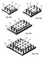
- FIG. 14 ashows a bottom perspective view of a carrier for a semiconductor die BGA type package according to an embodiment of the invention.
- FIG. 14 bshows a top perspective view of a carrier for a semiconductor die BGA type package according to an embodiment of the invention.
- FIG. 14 cshows a close up view of a bump and a conductive bridge of a carrier.
- FIG. 14 dshows a side view of a semiconductor die BGA type package with a wire bond.
- FIG. 14 eshows a side view of a semiconductor die BGA type package that has a flip chip type configuration.
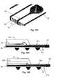
- FIGS. 15 a to 15 gshow side cross-sectional views of a stamping apparatus as it is used when forming a carrier according to an embodiment of the invention.
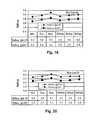
- FIG. 16shows a graph of the copper bump height vs. carrier sample.
- FIG. 17shows a graph of solder bump height distribution vs. package sample unit.
- FIG. 18shows a graph of the height difference of the copper bumps and the combined height of the solder balls, bond line, and semiconductor die in the package vs. package sample unit.
- FIGS. 19 and 20show graphs of RdSon for two different electrically tested lots.
- Embodiments of the inventionrelate to carriers for semiconductor die packages, semiconductor die packages including the carriers, methods for making the carriers, and the methods for assembling semiconductor die packages.
- the semiconductor die packagescan be, for example, MOSFET BGA packages, thin MOSFET packages, or any other type of semiconductor IC or discrete die package.
- the carriers according to embodiments of the inventioncomprise a metal layer such as a copper layer.
- Plural bumpsare formed in the metal layer and the bumps may be arranged in a predetermined configuration.
- the bumpsmay be in a regularly spaced array across the metal layer or may be at the periphery of the metal layer.
- the bumpsmay be arranged around a planar die attach region of the carrier.
- a semiconductor diecan then be attached to the die attach region using, for example, solder paste or a conductive adhesive.
- a number of solder paste depositse.g., solder balls
- solder ballscan be on the surface of the semiconductor die opposite the carrier.
- the bumpscan be formed by stamping a metal layer. Any suitable stamping apparatus may be used to form the bumps.
- An exemplary stamping apparatuscan comprise a stamping machine having multiple stamping elements (sometimes referred to as stamping tools), and a corresponding stamping die.
- the stamping diehas recesses that are configured to receive the multiple stamping elements.
- a metal layeris placed on the stamping die.
- the stamping elementspunch the metal layer while it is on the stamping die. During punching, the stamping elements push portions of the metal layer into the recesses of the stamping die without passing through the metal layer.
- the pressure applied to the metal layerdeforms portions of the metal layer to form multiple stamped bumps in the metal layer.
- This stamping processcan be repeated so that sets of bumps are formed in the metal layer. After stamping the sets of bumps, multiple carriers are formed. The formed carriers can be separated from each other after the semiconductor dies are assembled to the individual carriers to form individual packages. The separated packages can be mounted to a circuit substrate such as a circuit board.
- the carriercan be considered a “lead frame” that electrically couples a semiconductor die to a circuit substrate such as a circuit board.
- the embodiments of the inventionhave a number of advantages.
- the bumps in the carriercan replace interconnects that would otherwise be made using solder.
- less soldercan be used in the assembly of the semiconductor die packages.
- the embodiments of the inventionhave fewer solder balls as compared to other semiconductor die packages that have all solder balls as interconnects.
- Embodiments of the inventionare therefore more environmentally friendly than other types of semiconductor die packages.
- reducing the number of pure solder interconnectssimplifies the interconnect process. As the number of pure solder interconnects is reduced in embodiments of the invention, the number of solder balls that need to be placed on a semiconductor die or a circuit substrate is reduced.
- solder interconnectsare used in embodiments of the invention, the problems associated with forming many pure solder interconnects are reduced or eliminated.
- solder ballscan deform during processing.
- the solder ball heightsmay be inconsistent and the ends of the solder balls may not be coplanar with each other.
- the stamped bump interconnects in embodiments of the inventionare integrally formed in a carrier and are more robust than solder interconnects.
- stamped bumpscan be made with repeatable dimensions and can be consistently spaced with respect to each other. Also, compared to solder based interconnects, the stamped bumps exhibit superior electrical and thermal performance.
- the stamped bumps and the portion of the carrier that contacts the semiconductor diemay be formed from a single unitary material. Electrical current can flow from the portion that contacts the semiconductor die to the stamped bumps without passing through a material interface such as a solder to metal interface. Electrical current passes to the bumps without any loss in efficiency that might be caused by the presence of a material interface such as a solder to metal interface.
- the carriers according to embodiments of the inventioncan be manufactured in high volumes. Stamping interconnect structures is faster than mechanically placing solder balls on a circuit substrate or a semiconductor die.
- FIG. 2shows a semiconductor die package.
- the packagecomprises a carrier 20 comprising a metal layer that has a die attach region and a plurality of stamped bumps 26 around the die attach region.
- a semiconductor die 40comprising a vertical metal oxide semiconductor field effect transistor (MOSFET) is electrically coupled to and is proximate to the die attach region of the carrier 20 .
- Solder 42e.g., solder balls or solder columns
- solder balls or solder columnscan be on the semiconductor die 40 .
- FIG. 3shows a carrier 20 according to an embodiment of the invention.
- the carrier 20includes a number of stamped bumps 26 formed around a die attach region 24 .
- two windows 28are disposed around and at the periphery of the die attach region 24 .
- the windows 28are partially defined by tie bars 23 .
- the tie bars 23can be cut after a semiconductor die is attached to the die attach region 24 to form a functional unit of a MOSFET BGA package.
- Side rails 30are disposed on both sides of the carrier 20 . The side rails 30 hold the carriers and the portions of the processed metal layer that will be formed into carriers together during the stamping process.
- the carrier 20may comprise any suitable material.
- the carrier 20may comprise a base metal such as copper or aluminum. Metals such as these are good electrical and thermal conductors.
- the carrier 20can include a layer of metal that includes a base metal such as copper and one or more sublayers of material on the base metal. Exemplary sublayers may include adhesion layers, diffusion barriers, solder wettable layers, and oxidation barrier layers.
- the carrier 20 and the unstamped metal layer used to form the carriermay comprise a copper base coated with a metal such as a nickel-palladium alloy, nickel, or a nickel alloy.
- the layers on the base metalmay be formed before or after bumps are formed in the base metal.
- the carriercan comprise a dielectric material. Embodiments of this type are described in greater detail below with reference to FIGS. 14 a to 14 e.
- FIG. 4shows a stamped bump 26 according to an embodiment of the invention.
- the stamped bump 26is cone-shaped and includes a tip 26 a and a side portion 26 b.
- the tip 26 ais elevated with respect to the planar regions (e.g., a die attach region) of the carrier.
- the outer and/or inner surfaces of the tip 26 amay be curved and may have a partial spherical shape.
- the tip 26 a of the bump 26can be an interconnection point in the semiconductor die package.
- the tip 26 a of the bump 26can contact a conductive land on a circuit substrate (not shown) so that the circuit substrate and the bump 26 are in electrical communication with each other.
- the tip 26 a of the bump 26can be coupled to a conductive land using solder.
- the soldercan be deposited around and/or under the tip 26 a of the bump 26 to help stabilize the bump 26 on the land.
- the soldercan also help enhance the conductivity between the bump 26 and the land.
- the bumps in the carrier embodimentsmay have any suitable shape.
- FIGS. 5 to 8show examples of bumps with various shapes and dimensions.
- the stamped bumpsmay be cylindrical, round, square, etc. In some embodiments, the bumps are conical.
- the stamped bumps 26may also have any suitable size or height depending upon the particular semiconductor die package that the carrier will be incorporated in.
- FIG. 5shows a side cross-sectional view of stamped bumps in an exemplary carrier embodiment.
- the bump pitchis “P”.
- the bump pitch Pmay be the center-to-center distance of adjacent bumps in an array.
- the pitch Pmay be less than about 1 mm.
- the pitchmay be less than about 0.85 mm or less than about 0.65 mm (e.g., about 0.5 mm).
- the depth of the stampis “D”.
- the depth of the stamp Dmay be about 0.850 mm or less.
- the bump wall thicknessis “t”.
- the bump wall thickness tmay be less than about 0.10 mm.
- the carrier thicknessis “T”.
- the carrier thickness Tmay be, for example, about 0.300 mm or less in some embodiments.
- the height of the bumpis “H”.
- the height of the bumps Hmay be about 0.500 to about 0.550 mm, or less in some embodiments.
- the tips of the stamped bumpsare substantially coplanar. Because the bumps have tips that are substantially coplanar, all bumps in a carrier can contact conductive lands on a circuit substrate substantially simultaneously. Good electrical contact is made between the carrier bumps and the circuit substrate. Since all bumps contact the conductive lands at the same time, the likelihood of failure is due to a faulty interconnection between the conductive lands of a circuit substrate and the bumps is reduced. As will be explained in further detail below, a stamping process can be used to produce bumps with substantially coplanar tips. The stamped bumps are also robust and consistently positioned with respect to each other.
- FIG. 6shows another embodiment of the invention.
- the bumpsare cone-shaped.
- Each of the bumps shown in FIG. 6has a conical angle of less than about 40°.
- a “conical angle”can be an angle formed by opposing wall surfaces of a cone.
- Conescan be defined by the inner or outer surfaces of a bump in the carrier. Each of the inner surface and the outer surface of a bump may form a conical angle.
- Conescan also be defined by the outer surface of a tip of a stamping element or by the surface defining a recess in a stamping die. These surfaces may also form conical angles.
- the conical angles formed by the bumpsare wide.
- the conical angles (i.e., the angles formed by opposing inner or outer walls of the bump) of a bumpare greater than about 40°.
- the surfaces defining the recesses in a stamping die and the surface defining the stamping elementscan have conical angles of similar magnitude.
- the stamping elementscan be easily retracted from the recesses in the stamping die when forming the carrier. Bumps with large conical angles have a reduced likelihood of “sticking” to the stamping elements when they are withdrawn from the recesses of the stamping die. Bumps that stick to the stamping elements can be damaged in some cases.
- FIG. 7shows another bump according to an embodiment of the invention.
- a lower portion of the bumphas a conical angle of 90°.
- An upper portion of the bumpis cylindrically shaped and has a curved tip.
- a portion of the curved tipis substantially spherical.
- the inner radius of curvature of the spherical tip portionis about 0.150 mm, while the outer radius of curvature is about 0.250 mm.
- Other exemplary dimensionsare also shown in FIG. 7.
- the illustrated bumpis also conical.
- the portion of the bump at the tip of the bumphas a substantially spherical configuration.
- Each of the conical angles formed by the inner and the outer surfaces of the bumpis about 42° in this embodiment.
- a portion of the curved tipis substantially spherical.
- the inner radius of curvature of the spherical tip portionis about 0.158 mm, while the outer radius of curvature is about 0.250 mm.
- Other exemplary dimensionsare also shown in FIG. 8.
- FIG. 9shows the underside of the stamped bumps 26 in the backside of a carrier 20 .
- Each of the stamped bumpscan include hollow portions in the metal layer. As shown in FIG. 9, arrays of hollow portions are at the backside of the carrier. The shapes of the hollow portions can correspond to the shapes of the stamping elements used to form the stamped bumps.
- a semiconductor diecan be attached to the carrier.
- soft soldercan be applied to the die attach region of the carrier.
- a semiconductor diecan be placed on the soft solder and the semiconductor die can be attached to the carrier.
- a bond linecomprising the solder is formed between the carrier and the semiconductor die.
- the bond linemay have a thickness of about 1 mil (i.e., ⁇ fraction (1/1000) ⁇ th of an inch) or less.
- the solderflows towards the bumps at the periphery of the die attach region.
- a groove(not shown) may be provided in the carrier at the periphery of the die attach region to receive any solder that flows to the bumps.
- the groovemay be disposed between the bumps and the die attach region.
- a conductive adhesivesuch as a conductive epoxy adhesive may be used to attach the semiconductor die to the carrier.
- FIG. 10shows a semiconductor die package according to an embodiment of the invention.
- a semiconductor die 40is mounted to a die attach region of the carrier 20 .
- the stamped bumps 26are disposed around the die attach region and the semiconductor die 40 .
- the carrier 20is also intimately connected to the semiconductor die. Accordingly, the carrier 20 can act as a low resistance thermal and electrical conduction path for the semiconductor die 40 .
- the die packageis shown as being attached to other structures through side rails. The side rails can be cut to separate the package from these other structures.
- the semiconductor die 40may comprise any suitable electronic device.
- the semiconductor die 40may comprise a metal oxide field effect transistor (MOSFET) device such as a power MOSFET device.
- MOSFETmetal oxide field effect transistor
- the MOSFET devicemay have planar or trenched gate structures. Trenched gate structures are preferred. Transistor cells containing trenched gate structures are narrower than planar gate structures.
- the MOSFET devicemay be a vertical MOSFET device. In a vertical MOSFET device, the source region and the drain region are at opposite sides of the semiconductor die so that current in the transistor flows vertically through the semiconductor die.
- the semiconductor die 40may comprise silicon or any other suitable semiconductor material.
- the semiconductor die packages according to embodiments of the inventionare particularly well suited for discrete products with high heat dissipation such as power switching devices (e.g., power MOSFETs) where electrical connection to the backside of the die (MOSFET drain terminal) is required.
- power switching devicese.g., power MOSFETs
- MOSFET drain terminalelectrical connection to the backside of the die
- the packageprovides for a very low resistance, compact connection between the backside of the die (the drain terminal of the power MOSFET) and a circuit substrate (e.g., a PCB).
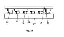
- FIG. 11shows a side view of a die package according to an embodiment of the invention.
- FIG. 11shows a semiconductor die 40 disposed between a circuit substrate 50 (e.g., a circuit board) and a carrier 20 .
- the carrier 20is coupled to the semiconductor die 40 through a bond line 44 .
- the bond line 44may comprise, for example, a conductive adhesive or solder.
- a number of solder interconnects 42are disposed between the semiconductor die 40 and the circuit substrate 50 .
- the semiconductor die 40 and the circuit substrate 50can communicate with each other through the solder interconnects 42 .
- Solder paste 46may be used to bond the stamped bumps 26 to the circuit substrate 50 .
- the semiconductor die 40 illustrated in FIG. 11may comprise a vertical MOSFET device.
- One or more of the solder interconnects 42can communicate with the source regions and the gate regions of the MOSFET in the semiconductor die 40 .
- the source region and the gate region of the MOSFET device in the semiconductor die 40are accessible through the underside of the semiconductor die 40 .
- the carrier 20can communicate with the drain region of the semiconductor die 40 .
- the drain region of the semiconductor die 40may be in contact with the bond line 44 . Drain current can flow through the bond line 44 , to the carrier 20 , laterally to the stamped bumps 26 and to the circuit substrate 50 .
- the semiconductor diecan be covered to protect it from the environment.
- a lidcan be attached to the circuit substrate and over the semiconductor die.
- an organic encapsulantcan be deposited on the semiconductor die and cured.
- FIGS. 12 a to 12 fshow the perspective views of semiconductor die package examples according to embodiments of the invention.
- the stamped bumps 26 in the carrier 20are disposed to one or more sides of the semiconductor die 40 .
- a line of stamped bumps 26can be at one, two, three, or four sides of a semiconductor die 40 .
- the tips of the stamped bumps 26are substantially coplanar with respect to each other and with the tips of the solder bumps 42 on the semiconductor dies 40 .
- Each of the semiconductor die packages shown in FIGS. 12 a to 12 fcan be flipped over and mounted to a circuit substrate (not shown).
- a circuit substrateupon which the die package portion is mounted can provide a transistor in the semiconductor die 40 with a gate connection, a source connection, and a drain connection.
- FIG. 13shows another embodiment of the invention.
- a portion of the semiconductor die 40is cut away to show the region underneath the semiconductor die 40 .
- Solder balls 42are disposed between the semiconductor die 40 and the carrier 20 . These solder balls 42 electrically couple the source and the gate regions (not shown) of a MOSFET device in the semiconductor die 40 to the carrier.
- the drain region of the MOSFET device in the semiconductor die 40 in this examplefaces upward and is distal to the carrier 20 , while the source and the gate regions are proximate to the carrier 20 .
- Most of the solder balls 42 under the semiconductor die 40are coupled to a first portion 20 - 1 of the carrier 20 .
- solder ballscan be coupled to the source regions in the MOSFET device in the semiconductor die 40 .
- the solder ball 42 -G on a second portion 20 - 2 of the carrier 20can be coupled to a gate region of the MOSFET device.
- Gate currentcan pass through a stamped bump 26 -G at the comer of the carrier 20 , through the second portion 20 - 2 of the carrier 20 , to the solder ball 42 -G, and to the semiconductor die 40 .
- a dielectric region 15is between the first and the second carrier portions 20 - 1 , 20 - 2 .
- the dielectric regionmay be, for example, a dielectric adhesive that joins the first and the second carrier portions 20 - 1 , 20 - 2 .
- the package shown in FIG. 13can be flipped over and mounted to a circuit substrate (not shown).
- the circuit substratecan have conductive lands corresponding to the drain region, the source region, and the gate region of the MOSFET.
- the carrier 20 shown in FIG. 13can be formed in any suitable manner.
- a rectangular metal layercan be stamped with bumps 26 , 26 -G.
- First and second carrier portions 20 - 1 , 20 - 2can be formed by cutting the metal layer. The cut line can correspond to the line formed by the dielectric region 15 . After cutting, the first and the second carrier portions 20 - 1 , 20 - 2 can be joined using a dielectric adhesive material (e.g., a dielectric epoxy adhesive).
- a dielectric adhesive materiale.g., a dielectric epoxy adhesive
- FIGS. 14 a to 14 eshow the application and use of a bumped carrier (e.g., a copper bumped carrier) in an IC (integrated circuit) BGA type die package.
- FIG. 14 ashows a carrier 22 with an array of stamped bumps 26 .
- Conductive traces 26 ae.g., conductive lines
- Both the stamped bumps 26 and the conductive traces 26 acan be present in a single metal layer.
- These conductive traces 26 acan be electrically coupled to traces on the other side of the carrier 22 .
- the tips of the stamped bumps 26are substantially coplanar. In comparison to the carrier shown in FIG.
- the bumps 26may be formed across the surface of the metal layer and not just at the periphery of a die attach region of the carrier 22 .
- the carrier shown in FIGS. 14 a to 14 ecan be an interposer that can be disposed between the semiconductor die and a circuit substrate (e.g., a circuit board).
- FIG. 14 bshows the opposite side of the carrier 22 as shown in FIG. 14 a.
- a semiconductor die(not shown) may be attached to a die attach region 37 of the carrier 22 . Leads to the attached semiconductor die can be electrically coupled to conductive lands 38 . Circuit traces 38 a lead to the conductive lands 38 and can be coupled to the circuit traces 26 a on the other side of the carrier 22 .
- FIG. 14 cis a close-up view of a bump 26 and the edge of the carrier.
- a conductive bridge 39is at the edge of a dielectric layer 30 and at the edge of the carrier. Conductive traces on opposite sides of the carrier can be coupled through the conductive bridge 39 (e.g., a conductive via).
- the conductive bridge 39is vertical with respect to the orientation of the carrier 22 .
- FIGS. 14 d to 14 eshow side cross-sectional views of IC-type packages using the carriers according to embodiments of the invention.
- FIG. 14 dshows an IC type package with a wire bond coupling a semiconductor die to the carrier.
- FIG. 14 eshows an IC chip type package where the semiconductor die is mounted in a flip-chip manner without a wire-bond. The semiconductor die communicates with the carrier through solder balls.
- the carriercomprises a metal layer with stamped bumps 26 and a conductive trace 26 a on a dielectric layer 30 .
- a conductive trace 36 ais on the side of the dielectric layer 30 opposite the conductive trace 26 a leading to the stamped bump 26 .
- An IC die 55is on the dielectric layer 30 and is electrically coupled to the circuit trace 36 a.
- a cover 56can cover the die 55 to protect the die 55 .
- the semiconductor die packages shown in FIGS. 14 d and 14 ecan be mounted to the conductive lands of a circuit substrate such as a circuit board.
- the stamped bumps 26can be soldered to conductive lands on the circuit substrate.
- the carrier shown in FIGS. 14 a to 14 ecan be formed in any suitable manner.
- a first metal layercan be stamped with a plurality of bumps.
- the first metal layercan then be bonded (e.g., using an adhesive or using a lamination process) to a dielectric layer.
- the first metal layercan be etched to form circuit traces.
- regions around a formed bump 26can be etched and the circuit trace 26 a that is formed can lead to the bump 26 .
- a second metal layercan then be bonded (e.g., using an adhesive or using a lamination process) to the side of the dielectric layer opposite the bumps.
- the second metal layercan then be etched to form conductive traces and conductive pads.
- a semiconductor diecan be mounted on the conductive pads.
- Conductive bridgese.g., vias
- Conductive bridgescan then be formed on the side of the dielectric layer or through the dielectric layer to communicate the conductive traces at opposite sides of the carrier.
- a semiconductor diecan be mounted to the conductive pads of the carrier using conventional processes. It is noted that the above-described process is a subtractive process. In other embodiments, it is possible to use an additive process to form conductive traces and conductive pads on the dielectric layer. Additive processes are well known in the art.
- many carrierscan be formed from a metal layer that is in the form of a strip.
- a planar metal layer 90is disposed on a stamping die 92 in a stamping apparatus.
- the stamping die 92has a number of cavities 92 ( a ) that correspond to the shapes of the bumps that will be formed in the metal layer 90 .
- Each of 10 the recesses 92 ( a )may define a conical shape.
- a stamper 80 including a plurality of stamping elements 80 ( a )is disposed above the stamping die 92 and the metal layer 90 .
- Each stamping element 80 ( a )may have a conical tip.
- the tips of the stamping elements 80 ( a )may be conical.
- Both the stamper 80 and the stamping die 92can comprise materials that are harder than the metal layer 90 .
- the stamper 90 and the stamping element 80can be made of steel, while the metal layer 90 may be made of copper.
- the metal layer 90can be a continuous sheet of copper.
- the stamping elements 80 ( a ) of the stamper 80may be cooperatively structured with the recesses 92 ( a ) in the stamping die 92 . During stamping, bumps are formed in the metal layer 90 .
- the pressure applied by the stamper 80can be selected according to the depth of the stamp desired, the particular product being produced, etc.
- the stamper 80may move in a downward direction toward the stamping die 92 .
- the stamping elements 80 ( a )contact the metal layer 90 and punch portions of the metal layer 90 to deform them.
- the stamping elements 80 ( a )pass into the cavity 92 ( a ) of the stamping die 92 until the deforming portions of the metal layer contact the ends of the cavity 92 ( a ).
- Portions of the metal layer 90are sandwiched between the walls defining the cavity 92 ( a ) and the tips of the stamping elements 92 ( a ).
- the portions of the metal layer 90conform to the spaces between the stamping elements 80 ( a ) and the stamping element tips.
- the ends of the cavity 92 ( a ) in the stamping dieare coplanar with each other. Consequently, the bumps formed in the cavity 92 ( a ) have tips that are coplanar with each other.
- the stamper 80is retracted and moves in an upward direction away from the stamping die 92 .
- the ends of the stamping elements 80 ( a ) of the stamper 80are withdrawn from the recesses in the stamping die 92 , while the stamped metal layer 90 remains on the stamping die 92 .
- the stamped metal layer 90can then be lifted off of the stamping die 92 .
- Another flat portion of the metal layer 90can then be placed over the recesses of the stamping die 92 .
- the flat portioncan be stamped to form another set of bumps for another carrier.
- semiconductor diescan be attached to the carriers in the strip using, for example, a conductive adhesive or solder.
- the carriers and semiconductor die unitscan then be marked, tested, and then separated into individual units. Additional packaging steps may also be performed.
- a number of stamped carriers with stamped bumpswere produced. Bumps were formed in copper layers according to the process generally illustrated in FIG. 15 a to 15 g.
- Semiconductor dies comprising vertical power MOSFETswere mounted to the carriers using solder to form a number of carrier/semiconductor die units. The carrier/semiconductor die units were then separated from each other. Each carrier/semiconductor die unit was then manually mounted to a 1 square inch chipboard using a 6337 type of solder paste (63% Sn and 37% Pb) to form die packages.
- the assembled die packageswere then processed in an infrared reflow oven. After the reflow process, each die package was inspected for adhesive strength and position accuracy. The resulting packages had a configuration similar to the one shown in FIG. 11.
- the graph in FIG. 16shows the copper bump height variation in different carriers.
- the heightvaried from about 21.05 to about 22.40 mils from a target of about 21.0 mils.
- the targeted copper bump heightwas based on the sum of the die thickness, the nominal solder bump height, and the bondline thickness, which were 8 mils, 12 mils, and 1 mil, respectively.
- solder bumps disposed between the semiconductor die and the chip boardwere also evaluated for height variation.
- the graph in FIG. 17shows the bump height variation from die-to-die.
- the solder bumpshad heights of about 11.2 mils to about 11.95 mils. There was no significant height difference between solder bumps for the gate and source terminals.
- FIG. 18measurements of the coplanarity of the solder bump height and copper bump height are shown.
- the average total height of the semiconductor die, the solder bumps, and the bondlinewas about 20.19 mils.
- the average height of the copper bumpswas about 21 mils.
- the average difference in the total height vs. the height of the copper bumpswas about 1 to about 2 mils. The data show that the copper bumps were almost perfectly coplanar with the solder bumps.
- the drain-to-source on-state resistance or RdSon(which is defined as the total resistance encountered by a drain current) in embodiments of the invention was comparable to the RdSon obtained in semiconductor die packages using solder bumps instead of stamped bumps as interconnects.
- the RdSon values for the copper bump embodimentswere about 3.5 to about 4.0 milliohms at 4.5V, and about 2.4 about 3.2 milliohms at about 10V.
- the RdSon values for the copper bump embodimentswere about 3.5 to about 4.0 milliohms at 4.5V, and about 2.4 and about 3.2 milliohms at 10V.
- the RdSon values shown in FIGS. 19 and 20are comparable to RdSon values obtained from a MOSFET BGA using solder balls as interconnects instead of stamped bumps.
Landscapes
- Engineering & Computer Science (AREA)
- Physics & Mathematics (AREA)
- Condensed Matter Physics & Semiconductors (AREA)
- General Physics & Mathematics (AREA)
- Computer Hardware Design (AREA)
- Microelectronics & Electronic Packaging (AREA)
- Power Engineering (AREA)
- Manufacturing & Machinery (AREA)
- Ceramic Engineering (AREA)
- Wire Bonding (AREA)
- Lead Frames For Integrated Circuits (AREA)
Abstract
Description
- Solder balls are used as electrical interconnects in ball grid array (BGA) packages. In a BGA package, an array of solder balls is used to couple a semiconductor die to a circuit substrate such as a printed circuit board (PCB).[0001]
- A method that can be used to form a BGA package is the solder ball attach process. In a solder ball attach process, solder balls are mechanically placed on a ball land pattern of conductive regions in a semiconductor carrier or substrate. After the solder balls are placed on the specified ball land pattern, the semiconductor die is flipped over and is mounted on a circuit substrate.[0002]
- The solder balls typically have a lead-based solder alloy. For example, the solder alloy may be a near eutectic tin-lead (Sn-Pb) alloy that melts at about 183° C. When the solder balls are present between the semiconductor die and the circuit substrate, the balls are heated to a temperature at or below the melting temperature of the solder alloy. The purpose of heating the balls below melting point is to ensure that the solder balls do not collapse. The solder balls are fluxed and re-flowed to join the circuit substrate to the semiconductor die. During fluxing, oxides in the solder are removed and the conductive surfaces of the semiconductor die and the circuit substrate are wet with the melting solder. After fluxing and re-flow, solder interconnects are formed between the semiconductor die and the circuit substrate. The formed solder interconnects electrically couple the circuit substrate and the semiconductor die together.[0003]
- FIG. 1 shows a semiconductor die package. In the die package, a[0004]
carrier 100 is provided with a rectangular cavity100-1 that receives asemiconductor die 102. In this example, the semiconductor die comprises a vertical metal oxide field effect transistor (MOSFET) and is in a Ball Grid Array-type package (BGA). An array ofsolder balls 108 is on the surface of semiconductor die102 as well as on anedge surface 106 of thecarrier 100. Thesolder ball array 108 is divided into two groups. A first outer array of solder balls108-2 connects to thecarrier edge surface 106 and an internal array of solder balls108-1 connects to the die surface. The array ofsolder balls 108 can be mounted and coupled to a circuit substrate such as a circuit board. - The outer array of solder balls[0005]108-2 provides the connection to the drain terminal of the MOSFET, while the inner array of solder balls108-1 provides the connection to the source and gate terminals of the MOSFET. A corner solder ball108-3 can be dedicated for the gate terminal and the remaining solder balls108-1 in the inner array108-1 provide for a distributed, low resistance connection to the source terminal of the BGA MOSFET.
- Solder ball technology could be enhanced and improved to provide for a more robust design. For example, the strength of adhesion of the ball interconnects could be improved. Solder interconnects formed using a ball attach process can break if they are weak. If one or more solder interconnects fail in a die package, the entire package can be inoperative. In addition, during processing (e.g., during reflow), the solder balls deform. The deformation can cause the solder balls in the array to have varying heights. As a result, the ends of the solder balls may not be coplanar with each other. If, for example, some of the solder balls on an array of conductive pads are taller than other solder balls in the array, the shorter solder balls may not make contact with both the semiconductor die and the circuit substrate. The formed die package could be inoperative due to the faulty solder interconnects. Also, solder balls can move during processing. If the solder balls move from their intended locations, the desired interconnections may not be formed in the semiconductor die package. Lastly, many solder balls contain lead. Lead is not an environmentally friendly substance. It would be desirable to reduce if not to eliminate the amount of lead used in a semiconductor die package.[0006]
- Embodiments of the invention address these and other problems.[0007]
- An embodiment of the invention is directed to a carrier for a semiconductor die package, the carrier comprising: (a) a metal layer; and (b) a plurality of bumps formed in the metal layer, wherein the carrier is for electrically coupling a semiconductor die to a circuit substrate.[0008]
- Another embodiment of the invention is directed to a semiconductor die package comprising: (a) a carrier comprising a metal layer, a die attach region, and a plurality of bumps formed in the metal layer; and (b) a semiconductor die electrically coupled to the die attach region of the carrier.[0009]
- Another embodiment of the invention is directed to a semiconductor die package comprising: (a) a carrier comprising metal layer, a die attach region, and a plurality of stamped bumps formed in the metal layer around the die attach region; (b) a semiconductor die comprising a vertical metal oxide semiconductor field effect transistor (MOSFET) device having a source region, a gate region, and a drain region, wherein the drain region is electrically coupled to and proximate to the die attach region of the carrier, and the source region and the gate region are distal to the die attach region, and wherein the plurality of stamped bumps in the carrier are arranged around the semiconductor die; and (c) a plurality of solder deposits disposed on the semiconductor die.[0010]
- Another embodiment of the invention is directed to a method for forming a carrier comprising: (a) providing a metal layer; and (b) forming a plurality of bumps in the metal layer to form the carrier.[0011]
- Another embodiment of the invention is directed to a method for forming a carrier for a semiconductor die package, the method comprising: (a) providing a metal layer; and (b) forming a plurality of bumps in the metal layer, wherein the formed bumps are capable of being electrically coupled to conductive regions of a circuit substrate.[0012]
- These and other embodiments of the invention are described in further detail below.[0013]
- FIG. 1 shows a perspective view of a semiconductor die package with solder balls.[0014]
- FIG. 2 shows a perspective view of a semiconductor die assembled on a carrier according to an embodiment of the invention.[0015]
- FIG. 3 shows a perspective view of a carrier according to an embodiment of the invention[0016]
- FIG. 4 shows a close-up, perspective view of bumps of a carrier embodiment.[0017]
- FIGS.[0018]5-8 show side cross-sectional views of bumps formed in carriers according to embodiments of the invention.
- FIG. 9 shows a perspective view of the underside of a carrier according to an embodiment of the invention.[0019]
- FIG. 10 shows a perspective view of a die package according to an embodiment of the invention.[0020]
- FIG. 11 shows a side view of a die package according to an embodiment of the invention.[0021]
- FIGS. 12[0022]ato12fshow perspective views of die packages according to embodiments of the invention.
- FIG. 13 shows a perspective view of a die package according to an embodiment of the invention where a portion of a semiconductor die is partially cut away to show solder balls underneath the semiconductor die.[0023]
- FIG. 14[0024]ashows a bottom perspective view of a carrier for a semiconductor die BGA type package according to an embodiment of the invention.
- FIG. 14[0025]bshows a top perspective view of a carrier for a semiconductor die BGA type package according to an embodiment of the invention.
- FIG. 14[0026]cshows a close up view of a bump and a conductive bridge of a carrier.
- FIG. 14[0027]dshows a side view of a semiconductor die BGA type package with a wire bond.
- FIG. 14[0028]eshows a side view of a semiconductor die BGA type package that has a flip chip type configuration.
- FIGS. 15[0029]ato15gshow side cross-sectional views of a stamping apparatus as it is used when forming a carrier according to an embodiment of the invention.
- FIG. 16 shows a graph of the copper bump height vs. carrier sample.[0030]
- FIG. 17 shows a graph of solder bump height distribution vs. package sample unit.[0031]
- FIG. 18 shows a graph of the height difference of the copper bumps and the combined height of the solder balls, bond line, and semiconductor die in the package vs. package sample unit.[0032]
- FIGS. 19 and 20 show graphs of RdSon for two different electrically tested lots.[0033]
- Embodiments of the invention relate to carriers for semiconductor die packages, semiconductor die packages including the carriers, methods for making the carriers, and the methods for assembling semiconductor die packages. The semiconductor die packages can be, for example, MOSFET BGA packages, thin MOSFET packages, or any other type of semiconductor IC or discrete die package.[0034]
- The carriers according to embodiments of the invention comprise a metal layer such as a copper layer. Plural bumps are formed in the metal layer and the bumps may be arranged in a predetermined configuration. For example, the bumps may be in a regularly spaced array across the metal layer or may be at the periphery of the metal layer. In some embodiments, the bumps may be arranged around a planar die attach region of the carrier. A semiconductor die can then be attached to the die attach region using, for example, solder paste or a conductive adhesive. A number of solder paste deposits (e.g., solder balls) can be on the surface of the semiconductor die opposite the carrier.[0035]
- The bumps can be formed by stamping a metal layer. Any suitable stamping apparatus may be used to form the bumps. An exemplary stamping apparatus can comprise a stamping machine having multiple stamping elements (sometimes referred to as stamping tools), and a corresponding stamping die. The stamping die has recesses that are configured to receive the multiple stamping elements. In an exemplary process, a metal layer is placed on the stamping die. The stamping elements punch the metal layer while it is on the stamping die. During punching, the stamping elements push portions of the metal layer into the recesses of the stamping die without passing through the metal layer. The pressure applied to the metal layer deforms portions of the metal layer to form multiple stamped bumps in the metal layer. This stamping process can be repeated so that sets of bumps are formed in the metal layer. After stamping the sets of bumps, multiple carriers are formed. The formed carriers can be separated from each other after the semiconductor dies are assembled to the individual carriers to form individual packages. The separated packages can be mounted to a circuit substrate such as a circuit board. In some embodiments, the carrier can be considered a “lead frame” that electrically couples a semiconductor die to a circuit substrate such as a circuit board.[0036]
- The embodiments of the invention have a number of advantages. For example, in embodiments of the invention, the bumps in the carrier can replace interconnects that would otherwise be made using solder. As a result, less solder can be used in the assembly of the semiconductor die packages. The embodiments of the invention have fewer solder balls as compared to other semiconductor die packages that have all solder balls as interconnects. Embodiments of the invention are therefore more environmentally friendly than other types of semiconductor die packages. In addition, reducing the number of pure solder interconnects simplifies the interconnect process. As the number of pure solder interconnects is reduced in embodiments of the invention, the number of solder balls that need to be placed on a semiconductor die or a circuit substrate is reduced. Moreover, because fewer solder interconnects are used in embodiments of the invention, the problems associated with forming many pure solder interconnects are reduced or eliminated. For example, as explained above, solder balls can deform during processing. The solder ball heights may be inconsistent and the ends of the solder balls may not be coplanar with each other. In comparison, the stamped bump interconnects in embodiments of the invention are integrally formed in a carrier and are more robust than solder interconnects. Unlike pure solder interconnects, stamped bumps can be made with repeatable dimensions and can be consistently spaced with respect to each other. Also, compared to solder based interconnects, the stamped bumps exhibit superior electrical and thermal performance. For example, in the carrier embodiments, the stamped bumps and the portion of the carrier that contacts the semiconductor die may be formed from a single unitary material. Electrical current can flow from the portion that contacts the semiconductor die to the stamped bumps without passing through a material interface such as a solder to metal interface. Electrical current passes to the bumps without any loss in efficiency that might be caused by the presence of a material interface such as a solder to metal interface. Also, the carriers according to embodiments of the invention can be manufactured in high volumes. Stamping interconnect structures is faster than mechanically placing solder balls on a circuit substrate or a semiconductor die.[0037]
- An embodiment of the invention is shown in FIG. 2. FIG. 2 shows a semiconductor die package. The package comprises a[0038]
carrier 20 comprising a metal layer that has a die attach region and a plurality of stampedbumps 26 around the die attach region. A semiconductor die40 comprising a vertical metal oxide semiconductor field effect transistor (MOSFET) is electrically coupled to and is proximate to the die attach region of thecarrier 20. Solder42 (e.g., solder balls or solder columns) can be on the semiconductor die40. - FIG. 3 shows a[0039]
carrier 20 according to an embodiment of the invention. Thecarrier 20 includes a number of stampedbumps 26 formed around a die attachregion 24. In this example, twowindows 28 are disposed around and at the periphery of the die attachregion 24. Thewindows 28 are partially defined by tie bars23. The tie bars23 can be cut after a semiconductor die is attached to the die attachregion 24 to form a functional unit of a MOSFET BGA package. Side rails30 are disposed on both sides of thecarrier 20. The side rails30 hold the carriers and the portions of the processed metal layer that will be formed into carriers together during the stamping process. - The[0040]
carrier 20 may comprise any suitable material. For example, thecarrier 20 may comprise a base metal such as copper or aluminum. Metals such as these are good electrical and thermal conductors. In some embodiments, thecarrier 20 can include a layer of metal that includes a base metal such as copper and one or more sublayers of material on the base metal. Exemplary sublayers may include adhesion layers, diffusion barriers, solder wettable layers, and oxidation barrier layers. For example, in some embodiments, thecarrier 20 and the unstamped metal layer used to form the carrier may comprise a copper base coated with a metal such as a nickel-palladium alloy, nickel, or a nickel alloy. The layers on the base metal may be formed before or after bumps are formed in the base metal. In yet other embodiments, the carrier can comprise a dielectric material. Embodiments of this type are described in greater detail below with reference to FIGS. 14ato14e. - FIG. 4 shows a stamped[0041]
bump 26 according to an embodiment of the invention. In this example, the stampedbump 26 is cone-shaped and includes atip 26aand a side portion26b.Thetip 26ais elevated with respect to the planar regions (e.g., a die attach region) of the carrier. The outer and/or inner surfaces of thetip 26amay be curved and may have a partial spherical shape. - The[0042]
tip 26aof thebump 26 can be an interconnection point in the semiconductor die package. For example, thetip 26aof thebump 26 can contact a conductive land on a circuit substrate (not shown) so that the circuit substrate and thebump 26 are in electrical communication with each other. In some embodiments, thetip 26aof thebump 26 can be coupled to a conductive land using solder. The solder can be deposited around and/or under thetip 26aof thebump 26 to help stabilize thebump 26 on the land. The solder can also help enhance the conductivity between thebump 26 and the land. Although solder can be used to join thebump 26 to a conductive land on a circuit substrate, less solder is used in embodiments of the invention than in a semiconductor die package having all pure solder interconnects. - The bumps in the carrier embodiments may have any suitable shape. FIGS.[0043]5 to8 show examples of bumps with various shapes and dimensions. The stamped bumps may be cylindrical, round, square, etc. In some embodiments, the bumps are conical. The stamped bumps26 may also have any suitable size or height depending upon the particular semiconductor die package that the carrier will be incorporated in.
- Exemplary carrier and bump dimensions such as the bump pitch, the stamp depth, the bump wall thickness, the carrier thickness, and the bump height can be described with reference to FIG. 5. FIG. 5 shows a side cross-sectional view of stamped bumps in an exemplary carrier embodiment. The bump pitch is “P”. The bump pitch P may be the center-to-center distance of adjacent bumps in an array. In some embodiments, the pitch P may be less than about 1 mm. For example, the pitch may be less than about 0.85 mm or less than about 0.65 mm (e.g., about 0.5 mm). The depth of the stamp is “D”. In some embodiments, the depth of the stamp D may be about 0.850 mm or less. The bump wall thickness is “t”. In some embodiments, the bump wall thickness t may be less than about 0.10 mm. The carrier thickness is “T”. The carrier thickness T may be, for example, about 0.300 mm or less in some embodiments. The height of the bump is “H”. The height of the bumps H may be about 0.500 to about 0.550 mm, or less in some embodiments. These and other specific dimensions are for purposes of illustration. It is understood that embodiments of the invention are not limited to carriers with the recited exemplary dimensions.[0044]
- In embodiments of the invention, the tips of the stamped bumps are substantially coplanar. Because the bumps have tips that are substantially coplanar, all bumps in a carrier can contact conductive lands on a circuit substrate substantially simultaneously. Good electrical contact is made between the carrier bumps and the circuit substrate. Since all bumps contact the conductive lands at the same time, the likelihood of failure is due to a faulty interconnection between the conductive lands of a circuit substrate and the bumps is reduced. As will be explained in further detail below, a stamping process can be used to produce bumps with substantially coplanar tips. The stamped bumps are also robust and consistently positioned with respect to each other.[0045]
- FIG. 6 shows another embodiment of the invention. In this embodiment, the bumps are cone-shaped. Each of the bumps shown in FIG. 6 has a conical angle of less than about 40°. A “conical angle” can be an angle formed by opposing wall surfaces of a cone. Cones can be defined by the inner or outer surfaces of a bump in the carrier. Each of the inner surface and the outer surface of a bump may form a conical angle. Cones can also be defined by the outer surface of a tip of a stamping element or by the surface defining a recess in a stamping die. These surfaces may also form conical angles.[0046]
- In preferred embodiments of the invention, the conical angles formed by the bumps are wide. Typically, the conical angles (i.e., the angles formed by opposing inner or outer walls of the bump) of a bump are greater than about 40°. The surfaces defining the recesses in a stamping die and the surface defining the stamping elements can have conical angles of similar magnitude. In these embodiments, the stamping elements can be easily retracted from the recesses in the stamping die when forming the carrier. Bumps with large conical angles have a reduced likelihood of “sticking” to the stamping elements when they are withdrawn from the recesses of the stamping die. Bumps that stick to the stamping elements can be damaged in some cases.[0047]
- FIG. 7 shows another bump according to an embodiment of the invention.[0048]
- A lower portion of the bump has a conical angle of 90°. An upper portion of the bump is cylindrically shaped and has a curved tip. A portion of the curved tip is substantially spherical. The inner radius of curvature of the spherical tip portion is about 0.150 mm, while the outer radius of curvature is about 0.250 mm. Other exemplary dimensions (in millimeters) are also shown in FIG. 7.[0049]
- In FIG. 8, the illustrated bump is also conical. The portion of the bump at the tip of the bump has a substantially spherical configuration. Each of the conical angles formed by the inner and the outer surfaces of the bump is about 42° in this embodiment. Like the bump shown in FIG. 5, a portion of the curved tip is substantially spherical. The inner radius of curvature of the spherical tip portion is about 0.158 mm, while the outer radius of curvature is about 0.250 mm. Other exemplary dimensions (in millimeters) are also shown in FIG. 8.[0050]
- FIG. 9 shows the underside of the stamped[0051]
bumps 26 in the backside of acarrier 20. Each of the stamped bumps can include hollow portions in the metal layer. As shown in FIG. 9, arrays of hollow portions are at the backside of the carrier. The shapes of the hollow portions can correspond to the shapes of the stamping elements used to form the stamped bumps. - Once the bumps are stamped and a carrier is formed, a semiconductor die can be attached to the carrier. For example, soft solder can be applied to the die attach region of the carrier. A semiconductor die can be placed on the soft solder and the semiconductor die can be attached to the carrier. After attaching the semiconductor die to the carrier, a bond line comprising the solder is formed between the carrier and the semiconductor die. In some embodiments, the bond line may have a thickness of about 1 mil (i.e., {fraction (1/1000)}th of an inch) or less. During the die attach step, the solder flows towards the bumps at the periphery of the die attach region. In some embodiments, a groove (not shown) may be provided in the carrier at the periphery of the die attach region to receive any solder that flows to the bumps. The groove may be disposed between the bumps and the die attach region. In other embodiments, a conductive adhesive such as a conductive epoxy adhesive may be used to attach the semiconductor die to the carrier.[0052]
- FIG. 10 shows a semiconductor die package according to an embodiment of the invention. A semiconductor die[0053]40 is mounted to a die attach region of the
carrier 20. The stamped bumps26 are disposed around the die attach region and the semiconductor die40. Thecarrier 20 is also intimately connected to the semiconductor die. Accordingly, thecarrier 20 can act as a low resistance thermal and electrical conduction path for the semiconductor die40. In this Figure, the die package is shown as being attached to other structures through side rails. The side rails can be cut to separate the package from these other structures. - The semiconductor die[0054]40 may comprise any suitable electronic device. For example, the semiconductor die40 may comprise a metal oxide field effect transistor (MOSFET) device such as a power MOSFET device. The MOSFET device may have planar or trenched gate structures. Trenched gate structures are preferred. Transistor cells containing trenched gate structures are narrower than planar gate structures. In addition, the MOSFET device may be a vertical MOSFET device. In a vertical MOSFET device, the source region and the drain region are at opposite sides of the semiconductor die so that current in the transistor flows vertically through the semiconductor die. The semiconductor die40 may comprise silicon or any other suitable semiconductor material.
- The semiconductor die packages according to embodiments of the invention are particularly well suited for discrete products with high heat dissipation such as power switching devices (e.g., power MOSFETs) where electrical connection to the backside of the die (MOSFET drain terminal) is required. By using a thermally and electrically conductive material such as copper for[0055]
carrier 20, the package provides for a very low resistance, compact connection between the backside of the die (the drain terminal of the power MOSFET) and a circuit substrate (e.g., a PCB). - FIG. 11 shows a side view of a die package according to an embodiment of the invention. FIG. 11 shows a[0056]
semiconductor die 40 disposed between a circuit substrate50 (e.g., a circuit board) and acarrier 20. Thecarrier 20 is coupled to the semiconductor die40 through abond line 44. Thebond line 44 may comprise, for example, a conductive adhesive or solder. A number of solder interconnects42 are disposed between the semiconductor die40 and thecircuit substrate 50. The semiconductor die40 and thecircuit substrate 50 can communicate with each other through the solder interconnects42.Solder paste 46 may be used to bond the stampedbumps 26 to thecircuit substrate 50. - The semiconductor die[0057]40 illustrated in FIG. 11 may comprise a vertical MOSFET device. One or more of the solder interconnects42 can communicate with the source regions and the gate regions of the MOSFET in the semiconductor die40. In this example, the source region and the gate region of the MOSFET device in the semiconductor die40 are accessible through the underside of the semiconductor die40. The
carrier 20 can communicate with the drain region of the semiconductor die40. In this example, the drain region of the semiconductor die40 may be in contact with thebond line 44. Drain current can flow through thebond line 44, to thecarrier 20, laterally to the stampedbumps 26 and to thecircuit substrate 50. - Once the semiconductor die is joined to the circuit substrate, the semiconductor die can be covered to protect it from the environment. In a typical package, a lid can be attached to the circuit substrate and over the semiconductor die. Alternatively, an organic encapsulant can be deposited on the semiconductor die and cured.[0058]
- FIGS. 12[0059]ato12fshow the perspective views of semiconductor die package examples according to embodiments of the invention. In each example, the stamped
bumps 26 in thecarrier 20 are disposed to one or more sides of the semiconductor die40. For instance, a line of stampedbumps 26 can be at one, two, three, or four sides of asemiconductor die 40. In each example, the tips of the stamped bumps26 are substantially coplanar with respect to each other and with the tips of the solder bumps42 on the semiconductor dies40. - Each of the semiconductor die packages shown in FIGS. 12[0060]ato12fcan be flipped over and mounted to a circuit substrate (not shown). When a die package is mounted to a circuit substrate, the tips of the solder bumps42 and the tips of the stamped bumps26 may contact conductive lands on a circuit substrate. The circuit substrate upon which the die package portion is mounted can provide a transistor in the semiconductor die40 with a gate connection, a source connection, and a drain connection.
- FIG. 13 shows another embodiment of the invention. In the FIG. 13, a portion of the semiconductor die[0061]40 is cut away to show the region underneath the semiconductor die40.
Solder balls 42 are disposed between the semiconductor die40 and thecarrier 20. Thesesolder balls 42 electrically couple the source and the gate regions (not shown) of a MOSFET device in the semiconductor die40 to the carrier. The drain region of the MOSFET device in the semiconductor die40 in this example faces upward and is distal to thecarrier 20, while the source and the gate regions are proximate to thecarrier 20. Most of thesolder balls 42 under the semiconductor die40 are coupled to a first portion20-1 of thecarrier 20. These solder balls can be coupled to the source regions in the MOSFET device in the semiconductor die40. The solder ball42-G on a second portion20-2 of thecarrier 20 can be coupled to a gate region of the MOSFET device. Gate current can pass through a stamped bump26-G at the comer of thecarrier 20, through the second portion20-2 of thecarrier 20, to the solder ball42-G, and to the semiconductor die40. Adielectric region 15 is between the first and the second carrier portions20-1,20-2. The dielectric region may be, for example, a dielectric adhesive that joins the first and the second carrier portions20-1,20-2. The package shown in FIG. 13 can be flipped over and mounted to a circuit substrate (not shown). The circuit substrate can have conductive lands corresponding to the drain region, the source region, and the gate region of the MOSFET. - The[0062]
carrier 20 shown in FIG. 13 can be formed in any suitable manner. For example, a rectangular metal layer can be stamped withbumps 26,26-G. First and second carrier portions20-1,20-2 can be formed by cutting the metal layer. The cut line can correspond to the line formed by thedielectric region 15. After cutting, the first and the second carrier portions20-1,20-2 can be joined using a dielectric adhesive material (e.g., a dielectric epoxy adhesive). - FIGS. 14[0063]ato14eshow the application and use of a bumped carrier (e.g., a copper bumped carrier) in an IC (integrated circuit) BGA type die package. FIG. 14ashows a
carrier 22 with an array of stamped bumps26. Conductive traces26a(e.g., conductive lines) are on thecarrier 22 and lead to the stamped bumps26. Both the stampedbumps 26 and theconductive traces 26a can be present in a single metal layer. These conductive traces26acan be electrically coupled to traces on the other side of thecarrier 22. As shown in FIG. 14a,the tips of the stamped bumps26 are substantially coplanar. In comparison to the carrier shown in FIG. 2, for example, thebumps 26 may be formed across the surface of the metal layer and not just at the periphery of a die attach region of thecarrier 22. Moreover, in comparison to the carrier shown in FIG. 2, for example, the carrier shown in FIGS. 14ato14ecan be an interposer that can be disposed between the semiconductor die and a circuit substrate (e.g., a circuit board). - FIG. 14[0064]bshows the opposite side of the
carrier 22 as shown in FIG. 14a.A semiconductor die (not shown) may be attached to a die attachregion 37 of thecarrier 22. Leads to the attached semiconductor die can be electrically coupled toconductive lands 38. Circuit traces38alead to theconductive lands 38 and can be coupled to the circuit traces26aon the other side of thecarrier 22. - FIG. 14[0065]cis a close-up view of a
bump 26 and the edge of the carrier. Aconductive bridge 39 is at the edge of adielectric layer 30 and at the edge of the carrier. Conductive traces on opposite sides of the carrier can be coupled through the conductive bridge39 (e.g., a conductive via). Theconductive bridge 39 is vertical with respect to the orientation of thecarrier 22. - FIGS. 14[0066]dto14eshow side cross-sectional views of IC-type packages using the carriers according to embodiments of the invention. FIG. 14dshows an IC type package with a wire bond coupling a semiconductor die to the carrier. FIG. 14eshows an IC chip type package where the semiconductor die is mounted in a flip-chip manner without a wire-bond. The semiconductor die communicates with the carrier through solder balls.
- In both FIGS. 14[0067]dand14e,the carrier comprises a metal layer with stamped
bumps 26 and aconductive trace 26aon adielectric layer 30. Aconductive trace 36ais on the side of thedielectric layer 30 opposite theconductive trace 26aleading to the stampedbump 26. An IC die55 is on thedielectric layer 30 and is electrically coupled to thecircuit trace 36a.Acover 56 can cover the die55 to protect thedie 55. - The semiconductor die packages shown in FIGS. 14[0068]dand14ecan be mounted to the conductive lands of a circuit substrate such as a circuit board. For example, the stamped
bumps 26 can be soldered to conductive lands on the circuit substrate. - The carrier shown in FIGS. 14[0069]ato14ecan be formed in any suitable manner. In one exemplary process, a first metal layer can be stamped with a plurality of bumps. The first metal layer can then be bonded (e.g., using an adhesive or using a lamination process) to a dielectric layer. After bonding, the first metal layer can be etched to form circuit traces. For example, as shown in FIG. 14c,regions around a formed
bump 26 can be etched and thecircuit trace 26athat is formed can lead to thebump 26. A second metal layer can then be bonded (e.g., using an adhesive or using a lamination process) to the side of the dielectric layer opposite the bumps. The second metal layer can then be etched to form conductive traces and conductive pads. A semiconductor die can be mounted on the conductive pads. Conductive bridges (e.g., vias) can then be formed on the side of the dielectric layer or through the dielectric layer to communicate the conductive traces at opposite sides of the carrier. After the carrier is formed, a semiconductor die can be mounted to the conductive pads of the carrier using conventional processes. It is noted that the above-described process is a subtractive process. In other embodiments, it is possible to use an additive process to form conductive traces and conductive pads on the dielectric layer. Additive processes are well known in the art. - In some embodiments, many carriers can be formed from a metal layer that is in the form of a strip. Referring to FIG. 15[0070]a,a
planar metal layer 90 is disposed on a stamping die92 in a stamping apparatus. The stamping die92 has a number of cavities92(a) that correspond to the shapes of the bumps that will be formed in themetal layer 90. Each of10 the recesses92(a) may define a conical shape. Astamper 80 including a plurality of stamping elements80(a) is disposed above the stamping die92 and themetal layer 90. Each stamping element80(a) may have a conical tip. The tips of the stamping elements80(a) may be conical. Both thestamper 80 and the stamping die92 can comprise materials that are harder than themetal layer 90. For example, in some embodiments, thestamper 90 and the stampingelement 80 can be made of steel, while themetal layer 90 may be made of copper. Themetal layer 90 can be a continuous sheet of copper. In addition, the stamping elements80(a) of thestamper 80 may be cooperatively structured with the recesses92(a) in the stamping die92. During stamping, bumps are formed in themetal layer 90. The pressure applied by thestamper 80 can be selected according to the depth of the stamp desired, the particular product being produced, etc. - Referring to FIGS. 15[0071]band15e,the
stamper 80 may move in a downward direction toward the stamping die92. The stamping elements80(a) contact themetal layer 90 and punch portions of themetal layer 90 to deform them. During punching, the stamping elements80(a) pass into the cavity92(a) of the stamping die92 until the deforming portions of the metal layer contact the ends of the cavity92(a). Portions of themetal layer 90 are sandwiched between the walls defining the cavity92(a) and the tips of the stamping elements92(a). The portions of themetal layer 90 conform to the spaces between the stamping elements80(a) and the stamping element tips. The ends of the cavity92(a) in the stamping die are coplanar with each other. Consequently, the bumps formed in the cavity92(a) have tips that are coplanar with each other. - As shown in FIG. 15[0072]f,after stamping the
metal layer 90, thestamper 80 is retracted and moves in an upward direction away from the stamping die92. The ends of the stamping elements80(a) of thestamper 80 are withdrawn from the recesses in the stamping die92, while the stampedmetal layer 90 remains on the stamping die92. - Referring to FIG. 15[0073]g,after the
stamper 80 is retracted, the stampedmetal layer 90 can then be lifted off of the stamping die92. Another flat portion of themetal layer 90 can then be placed over the recesses of the stamping die92. The flat portion can be stamped to form another set of bumps for another carrier. - Once multiple bumped carriers are formed in the metal strip, semiconductor dies can be attached to the carriers in the strip using, for example, a conductive adhesive or solder. The carriers and semiconductor die units can then be marked, tested, and then separated into individual units. Additional packaging steps may also be performed.[0074]
- A number of stamped carriers with stamped bumps were produced. Bumps were formed in copper layers according to the process generally illustrated in FIG. 15[0075]ato15g.Semiconductor dies comprising vertical power MOSFETs were mounted to the carriers using solder to form a number of carrier/semiconductor die units. The carrier/semiconductor die units were then separated from each other. Each carrier/semiconductor die unit was then manually mounted to a 1 square inch chipboard using a 6337 type of solder paste (63% Sn and 37% Pb) to form die packages. The assembled die packages were then processed in an infrared reflow oven. After the reflow process, each die package was inspected for adhesive strength and position accuracy. The resulting packages had a configuration similar to the one shown in FIG. 11.
- A number of characteristics were evaluated in the formed packages. The copper bump height distribution, the solder bump height distribution, and the coplanarity of the solder bumps and copper bumps with respect to a die attach pad (DAP) were evaluated. The on-state resistance, RdSon, was also evaluated.[0076]
- The graph in FIG. 16 shows the copper bump height variation in different carriers. The height varied from about 21.05 to about 22.40 mils from a target of about 21.0 mils. The targeted copper bump height was based on the sum of the die thickness, the nominal solder bump height, and the bondline thickness, which were 8 mils, 12 mils, and 1 mil, respectively.[0077]
- The solder bumps disposed between the semiconductor die and the chip board were also evaluated for height variation. The graph in FIG. 17 shows the bump height variation from die-to-die. The solder bumps had heights of about 11.2 mils to about 11.95 mils. There was no significant height difference between solder bumps for the gate and source terminals.[0078]
- In FIG. 18, measurements of the coplanarity of the solder bump height and copper bump height are shown. Using the die attach pad as a reference, the average total height of the semiconductor die, the solder bumps, and the bondline was about 20.19 mils. The average height of the copper bumps was about 21 mils. The average difference in the total height vs. the height of the copper bumps was about 1 to about 2 mils. The data show that the copper bumps were almost perfectly coplanar with the solder bumps.[0079]
- Electrical tests were also conducted to evaluate the properties of the stamped bumps. In particular, the drain-to-source on-state resistance or RdSon (which is defined as the total resistance encountered by a drain current) in embodiments of the invention was comparable to the RdSon obtained in semiconductor die packages using solder bumps instead of stamped bumps as interconnects. With reference to FIG. 19, the RdSon values for the copper bump embodiments were about 3.5 to about 4.0 milliohms at 4.5V, and about 2.4 about 3.2 milliohms at about 10V. With reference to FIG. 20, the RdSon values for the copper bump embodiments were about 3.5 to about 4.0 milliohms at 4.5V, and about 2.4 and about 3.2 milliohms at 10V. The RdSon values shown in FIGS. 19 and 20 are comparable to RdSon values obtained from a MOSFET BGA using solder balls as interconnects instead of stamped bumps.[0080]
- The terms and expressions which have been employed herein are used as terms of description and not of limitation. There is no intention in the use of such terms and expressions of excluding equivalents of the features as shown and described. The portions thereof, are recognized that various modifications are possible within the scope of the invention as claimed. Moreover, any one or more features of any embodiment of the invention may be combined with any one or more other features of any other embodiment of the invention, without departing from the scope of the invention.[0081]
Claims (28)
Priority Applications (7)
| Application Number | Priority Date | Filing Date | Title |
|---|---|---|---|
| US09/855,820US6893901B2 (en) | 2001-05-14 | 2001-05-14 | Carrier with metal bumps for semiconductor die packages |
| PCT/US2002/014171WO2002093646A1 (en) | 2001-05-14 | 2002-05-02 | Carrier with metal bumps for semiconductor die packages |
| JP2002590418AJP4177119B2 (en) | 2001-05-14 | 2002-05-02 | Carrier with metal protrusions for semiconductor die packages |
| KR1020037014833AKR100944472B1 (en) | 2001-05-14 | 2002-05-02 | Carrier with metal bumps for semiconductor die packages |
| TW091109917ATW544885B (en) | 2001-05-14 | 2002-05-13 | Carrier with metal bumps for semiconductor die packages |
| US10/799,895US7023077B2 (en) | 2001-05-14 | 2004-03-11 | Carrier with metal bumps for semiconductor die packages |
| US11/342,027US20060131747A1 (en) | 2001-05-14 | 2006-01-27 | Carrier with metal bumps for semiconductor die packages |
Applications Claiming Priority (1)
| Application Number | Priority Date | Filing Date | Title |
|---|---|---|---|
| US09/855,820US6893901B2 (en) | 2001-05-14 | 2001-05-14 | Carrier with metal bumps for semiconductor die packages |
Related Child Applications (1)
| Application Number | Title | Priority Date | Filing Date |
|---|---|---|---|
| US10/799,895DivisionUS7023077B2 (en) | 2001-05-14 | 2004-03-11 | Carrier with metal bumps for semiconductor die packages |
Publications (2)
| Publication Number | Publication Date |
|---|---|
| US20020167075A1true US20020167075A1 (en) | 2002-11-14 |
| US6893901B2 US6893901B2 (en) | 2005-05-17 |
Family
ID=25322147
Family Applications (3)
| Application Number | Title | Priority Date | Filing Date |
|---|---|---|---|
| US09/855,820Expired - Fee RelatedUS6893901B2 (en) | 2001-05-14 | 2001-05-14 | Carrier with metal bumps for semiconductor die packages |
| US10/799,895Expired - Fee RelatedUS7023077B2 (en) | 2001-05-14 | 2004-03-11 | Carrier with metal bumps for semiconductor die packages |
| US11/342,027AbandonedUS20060131747A1 (en) | 2001-05-14 | 2006-01-27 | Carrier with metal bumps for semiconductor die packages |
Family Applications After (2)
| Application Number | Title | Priority Date | Filing Date |
|---|---|---|---|
| US10/799,895Expired - Fee RelatedUS7023077B2 (en) | 2001-05-14 | 2004-03-11 | Carrier with metal bumps for semiconductor die packages |
| US11/342,027AbandonedUS20060131747A1 (en) | 2001-05-14 | 2006-01-27 | Carrier with metal bumps for semiconductor die packages |
Country Status (5)
| Country | Link |
|---|---|
| US (3) | US6893901B2 (en) |
| JP (1) | JP4177119B2 (en) |
| KR (1) | KR100944472B1 (en) |
| TW (1) | TW544885B (en) |
| WO (1) | WO2002093646A1 (en) |
Cited By (14)
| Publication number | Priority date | Publication date | Assignee | Title |
|---|---|---|---|---|
| US20030071331A1 (en)* | 2001-10-17 | 2003-04-17 | Yoshihide Yamaguchi | Semiconductor device and structure for mounting the same |
| US6777800B2 (en) | 2002-09-30 | 2004-08-17 | Fairchild Semiconductor Corporation | Semiconductor die package including drain clip |
| US20040207052A1 (en)* | 2002-08-30 | 2004-10-21 | Rajeev Joshi | Substrate based unmolded package |
| US20050218300A1 (en)* | 2004-04-02 | 2005-10-06 | Quinones Maria Clemens Y | Surface mount multi-channel optocoupler |
| US20060250239A1 (en)* | 2005-05-06 | 2006-11-09 | Melton Randall W | Security method for data protection |
| US20070001278A1 (en)* | 2005-06-30 | 2007-01-04 | Oseob Jeon | Semiconductor die package and method for making the same |
| US20070015316A1 (en)* | 2005-07-12 | 2007-01-18 | Madrid Ruben P | Folded frame carrier for MOSFET BGA |
| US20070202715A1 (en)* | 2004-08-19 | 2007-08-30 | Daily Christopher G | Electrical connector with stepped housing |
| US20070215997A1 (en)* | 2006-03-17 | 2007-09-20 | Martin Standing | Chip-scale package |
| US20080315410A1 (en)* | 2007-06-21 | 2008-12-25 | Johnson Alan E | Substrate Including Barrier Solder Bumps to Control Underfill Transgression and Microelectronic Package including Same |
| US7518223B2 (en)* | 2001-08-24 | 2009-04-14 | Micron Technology, Inc. | Semiconductor devices and semiconductor device assemblies including a nonconfluent spacer layer |
| US7825502B2 (en) | 2008-01-09 | 2010-11-02 | Fairchild Semiconductor Corporation | Semiconductor die packages having overlapping dice, system using the same, and methods of making the same |
| EP2639828A3 (en)* | 2012-03-14 | 2013-11-20 | Robert Bosch GmbH | Circuit support assembly |
| DE102015115999B4 (en)* | 2014-09-23 | 2021-05-27 | Infineon Technologies Ag | Electronic component |
Families Citing this family (59)
| Publication number | Priority date | Publication date | Assignee | Title |
|---|---|---|---|---|
| IL133453A0 (en)* | 1999-12-10 | 2001-04-30 | Shellcase Ltd | Methods for producing packaged integrated circuit devices and packaged integrated circuit devices produced thereby |
| US10388626B2 (en)* | 2000-03-10 | 2019-08-20 | STATS ChipPAC Pte. Ltd. | Semiconductor device and method of forming flipchip interconnect structure |
| ATE459099T1 (en)* | 2000-03-10 | 2010-03-15 | Chippac Inc | FLIPCHIP CONNECTION STRUCTURE AND PROCESS OF PRODUCTION THEREOF |
| KR101075169B1 (en)* | 2003-08-27 | 2011-10-19 | 페어차일드코리아반도체 주식회사 | Power module flip chip package |
| TWI239087B (en)* | 2004-07-23 | 2005-09-01 | Siliconware Precision Industries Co Ltd | Flip-chip semiconductor package with lead frame and method for fabricating the same |
| US7183140B2 (en)* | 2004-11-08 | 2007-02-27 | Intel Corporation | Injection molded metal bonding tray for integrated circuit device fabrication |
| US7786558B2 (en)* | 2005-10-20 | 2010-08-31 | Infineon Technologies Ag | Semiconductor component and methods to produce a semiconductor component |
| US7285849B2 (en)* | 2005-11-18 | 2007-10-23 | Fairchild Semiconductor Corporation | Semiconductor die package using leadframe and clip and method of manufacturing |
| US20090057852A1 (en)* | 2007-08-27 | 2009-03-05 | Madrid Ruben P | Thermally enhanced thin semiconductor package |
| US7371616B2 (en)* | 2006-01-05 | 2008-05-13 | Fairchild Semiconductor Corporation | Clipless and wireless semiconductor die package and method for making the same |
| US20070164428A1 (en)* | 2006-01-18 | 2007-07-19 | Alan Elbanhawy | High power module with open frame package |
| US7868432B2 (en)* | 2006-02-13 | 2011-01-11 | Fairchild Semiconductor Corporation | Multi-chip module for battery power control |
| US7663212B2 (en)* | 2006-03-21 | 2010-02-16 | Infineon Technologies Ag | Electronic component having exposed surfaces |
| US7768075B2 (en)* | 2006-04-06 | 2010-08-03 | Fairchild Semiconductor Corporation | Semiconductor die packages using thin dies and metal substrates |
| US7618896B2 (en) | 2006-04-24 | 2009-11-17 | Fairchild Semiconductor Corporation | Semiconductor die package including multiple dies and a common node structure |
| US7541681B2 (en)* | 2006-05-04 | 2009-06-02 | Infineon Technologies Ag | Interconnection structure, electronic component and method of manufacturing the same |
| US7656024B2 (en) | 2006-06-30 | 2010-02-02 | Fairchild Semiconductor Corporation | Chip module for complete power train |
| US7564124B2 (en)* | 2006-08-29 | 2009-07-21 | Fairchild Semiconductor Corporation | Semiconductor die package including stacked dice and heat sink structures |
| US8106501B2 (en)* | 2008-12-12 | 2012-01-31 | Fairchild Semiconductor Corporation | Semiconductor die package including low stress configuration |
| US7768105B2 (en) | 2007-01-24 | 2010-08-03 | Fairchild Semiconductor Corporation | Pre-molded clip structure |
| US7821116B2 (en)* | 2007-02-05 | 2010-10-26 | Fairchild Semiconductor Corporation | Semiconductor die package including leadframe with die attach pad with folded edge |
| KR101391925B1 (en)* | 2007-02-28 | 2014-05-07 | 페어차일드코리아반도체 주식회사 | Semiconductor package and semiconductor package mold for fabricating the same |
| KR101489325B1 (en) | 2007-03-12 | 2015-02-06 | 페어차일드코리아반도체 주식회사 | Flip-chip type stacked power module and method of manufacturing the power module |
| US7659531B2 (en)* | 2007-04-13 | 2010-02-09 | Fairchild Semiconductor Corporation | Optical coupler package |
| US7683463B2 (en)* | 2007-04-19 | 2010-03-23 | Fairchild Semiconductor Corporation | Etched leadframe structure including recesses |
| US7902657B2 (en)* | 2007-08-28 | 2011-03-08 | Fairchild Semiconductor Corporation | Self locking and aligning clip structure for semiconductor die package |
| US7737548B2 (en) | 2007-08-29 | 2010-06-15 | Fairchild Semiconductor Corporation | Semiconductor die package including heat sinks |
| US20090057855A1 (en)* | 2007-08-30 | 2009-03-05 | Maria Clemens Quinones | Semiconductor die package including stand off structures |
| US20090065931A1 (en)* | 2007-09-11 | 2009-03-12 | Intel Corporation | Packaged integrated circuit and method of forming thereof |
| US7589338B2 (en)* | 2007-11-30 | 2009-09-15 | Fairchild Semiconductor Corporation | Semiconductor die packages suitable for optoelectronic applications having clip attach structures for angled mounting of dice |
| US20090140266A1 (en)* | 2007-11-30 | 2009-06-04 | Yong Liu | Package including oriented devices |
| KR20090062612A (en)* | 2007-12-13 | 2009-06-17 | 페어차일드코리아반도체 주식회사 | Multi-chip package |
| US7781872B2 (en)* | 2007-12-19 | 2010-08-24 | Fairchild Semiconductor Corporation | Package with multiple dies |
| US20090166826A1 (en)* | 2007-12-27 | 2009-07-02 | Janducayan Omar A | Lead frame die attach paddles with sloped walls and backside grooves suitable for leadless packages |
| US8106406B2 (en)* | 2008-01-09 | 2012-01-31 | Fairchild Semiconductor Corporation | Die package including substrate with molded device |
| US7791084B2 (en) | 2008-01-09 | 2010-09-07 | Fairchild Semiconductor Corporation | Package with overlapping devices |
| US7626249B2 (en)* | 2008-01-10 | 2009-12-01 | Fairchild Semiconductor Corporation | Flex clip connector for semiconductor device |
| US20090194857A1 (en)* | 2008-02-01 | 2009-08-06 | Yong Liu | Thin Compact Semiconductor Die Packages Suitable for Smart-Power Modules, Methods of Making the Same, and Systems Using the Same |
| US20090194856A1 (en)* | 2008-02-06 | 2009-08-06 | Gomez Jocel P | Molded package assembly |
| KR101524545B1 (en)* | 2008-02-28 | 2015-06-01 | 페어차일드코리아반도체 주식회사 | Power device package and the method of fabricating the same |
| US8018054B2 (en)* | 2008-03-12 | 2011-09-13 | Fairchild Semiconductor Corporation | Semiconductor die package including multiple semiconductor dice |
| US7915721B2 (en)* | 2008-03-12 | 2011-03-29 | Fairchild Semiconductor Corporation | Semiconductor die package including IC driver and bridge |
| US7768108B2 (en)* | 2008-03-12 | 2010-08-03 | Fairchild Semiconductor Corporation | Semiconductor die package including embedded flip chip |
| KR101519062B1 (en)* | 2008-03-31 | 2015-05-11 | 페어차일드코리아반도체 주식회사 | Semiconductor Device Package |
| US20090278241A1 (en)* | 2008-05-08 | 2009-11-12 | Yong Liu | Semiconductor die package including die stacked on premolded substrate including die |
| US7745244B2 (en) | 2008-06-23 | 2010-06-29 | Fairchild Semiconductor Corporation | Pin substrate and package |
| US7855439B2 (en)* | 2008-08-28 | 2010-12-21 | Fairchild Semiconductor Corporation | Molded ultra thin semiconductor die packages, systems using the same, and methods of making the same |
| US7829988B2 (en)* | 2008-09-22 | 2010-11-09 | Fairchild Semiconductor Corporation | Stacking quad pre-molded component packages, systems using the same, and methods of making the same |
| US8314499B2 (en)* | 2008-11-14 | 2012-11-20 | Fairchild Semiconductor Corporation | Flexible and stackable semiconductor die packages having thin patterned conductive layers |
| US8193618B2 (en) | 2008-12-12 | 2012-06-05 | Fairchild Semiconductor Corporation | Semiconductor die package with clip interconnection |
| US7973393B2 (en)* | 2009-02-04 | 2011-07-05 | Fairchild Semiconductor Corporation | Stacked micro optocouplers and methods of making the same |
| US8222718B2 (en)* | 2009-02-05 | 2012-07-17 | Fairchild Semiconductor Corporation | Semiconductor die package and method for making the same |
| US8563360B2 (en)* | 2009-06-08 | 2013-10-22 | Alpha And Omega Semiconductor, Inc. | Power semiconductor device package and fabrication method |
| US7939370B1 (en)* | 2009-10-29 | 2011-05-10 | Alpha And Omega Semiconductor Incorporated | Power semiconductor package |
| US8344495B2 (en)* | 2009-12-11 | 2013-01-01 | Stats Chippac Ltd. | Integrated circuit packaging system with interconnect and method of manufacture thereof |
| US8421204B2 (en) | 2011-05-18 | 2013-04-16 | Fairchild Semiconductor Corporation | Embedded semiconductor power modules and packages |
| US9679862B2 (en)* | 2014-11-28 | 2017-06-13 | Taiwan Semiconductor Manufacturing Company Ltd. | Semiconductor device having conductive bumps of varying heights |
| CN107993991B (en)* | 2017-12-20 | 2024-10-01 | 合肥矽迈微电子科技有限公司 | Chip packaging structure and manufacturing method thereof |
| US20200321272A1 (en)* | 2019-03-07 | 2020-10-08 | Skyworks Solutions, Inc. | Module with ball grid array having increased die area |
Family Cites Families (13)
| Publication number | Priority date | Publication date | Assignee | Title |
|---|---|---|---|---|
| US5123163A (en)* | 1989-04-27 | 1992-06-23 | Nec Corporation | Process and apparatus for forming bumps on film carrier |
| US5214307A (en)* | 1991-07-08 | 1993-05-25 | Micron Technology, Inc. | Lead frame for semiconductor devices having improved adhesive bond line control |
| KR100369681B1 (en)* | 1994-07-14 | 2003-04-11 | 서직스 코퍼레이션 | Variable voltage protection structures and method for making same |
| JPH08288424A (en)* | 1995-04-18 | 1996-11-01 | Nec Corp | Semiconductor device |
| US6144101A (en)* | 1996-12-03 | 2000-11-07 | Micron Technology, Inc. | Flip chip down-bond: method and apparatus |
| US5831832A (en)* | 1997-08-11 | 1998-11-03 | Motorola, Inc. | Molded plastic ball grid array package |
| JPH11312749A (en)* | 1998-02-25 | 1999-11-09 | Fujitsu Ltd | Semiconductor device, method of manufacturing the same, and method of manufacturing a lead frame |
| US6133634A (en) | 1998-08-05 | 2000-10-17 | Fairchild Semiconductor Corporation | High performance flip chip package |
| EP0978871A3 (en) | 1998-08-05 | 2001-12-19 | Harris Corporation | A low power packaging design |
| US6137165A (en)* | 1999-06-25 | 2000-10-24 | International Rectifier Corp. | Hybrid package including a power MOSFET die and a control and protection circuit die with a smaller sense MOSFET |
| US6864423B2 (en)* | 2000-12-15 | 2005-03-08 | Semiconductor Component Industries, L.L.C. | Bump chip lead frame and package |
| US6645791B2 (en)* | 2001-04-23 | 2003-11-11 | Fairchild Semiconductor | Semiconductor die package including carrier with mask |
| US6489204B1 (en)* | 2001-08-20 | 2002-12-03 | Episil Technologies, Inc. | Save MOS device |
- 2001
- 2001-05-14USUS09/855,820patent/US6893901B2/ennot_activeExpired - Fee Related
- 2002
- 2002-05-02JPJP2002590418Apatent/JP4177119B2/ennot_activeExpired - Fee Related
- 2002-05-02KRKR1020037014833Apatent/KR100944472B1/ennot_activeExpired - Fee Related
- 2002-05-02WOPCT/US2002/014171patent/WO2002093646A1/enactiveApplication Filing
- 2002-05-13TWTW091109917Apatent/TW544885B/ennot_activeIP Right Cessation
- 2004
- 2004-03-11USUS10/799,895patent/US7023077B2/ennot_activeExpired - Fee Related
- 2006
- 2006-01-27USUS11/342,027patent/US20060131747A1/ennot_activeAbandoned
Cited By (34)
| Publication number | Priority date | Publication date | Assignee | Title |
|---|---|---|---|---|
| US7518223B2 (en)* | 2001-08-24 | 2009-04-14 | Micron Technology, Inc. | Semiconductor devices and semiconductor device assemblies including a nonconfluent spacer layer |
| US7084498B2 (en)* | 2001-10-17 | 2006-08-01 | Renesas Technology Corp. | Semiconductor device having projected electrodes and structure for mounting the same |
| US20030071331A1 (en)* | 2001-10-17 | 2003-04-17 | Yoshihide Yamaguchi | Semiconductor device and structure for mounting the same |
| US20060003492A1 (en)* | 2002-08-30 | 2006-01-05 | Rajeev Joshi | Substrate based unmolded package |
| US7682877B2 (en) | 2002-08-30 | 2010-03-23 | Fairchild Semiconductor Corporation | Substrate based unmolded package |
| US20060006550A1 (en)* | 2002-08-30 | 2006-01-12 | Rajeev Joshi | Substrate based unmolded package |
| US7061077B2 (en)* | 2002-08-30 | 2006-06-13 | Fairchild Semiconductor Corporation | Substrate based unmolded package including lead frame structure and semiconductor die |
| US7439613B2 (en) | 2002-08-30 | 2008-10-21 | Fairchild Semicondcutor Corporation | Substrate based unmolded package |
| US20040207052A1 (en)* | 2002-08-30 | 2004-10-21 | Rajeev Joshi | Substrate based unmolded package |
| US8541890B2 (en) | 2002-08-30 | 2013-09-24 | Fairchild Semiconductor Corporation | Substrate based unmolded package |
| US7790513B2 (en) | 2002-08-30 | 2010-09-07 | Fairchild Semiconductor Corporation | Substrate based unmolded package |
| US20090130802A1 (en)* | 2002-08-30 | 2009-05-21 | Rajeev Joshi | Substrate based unmolded package |
| US7504281B2 (en) | 2002-08-30 | 2009-03-17 | Fairchild Semiconductor Corporation | Substrate based unmolded package |
| US6777800B2 (en) | 2002-09-30 | 2004-08-17 | Fairchild Semiconductor Corporation | Semiconductor die package including drain clip |
| US7196313B2 (en) | 2004-04-02 | 2007-03-27 | Fairchild Semiconductor Corporation | Surface mount multi-channel optocoupler |
| US20050218300A1 (en)* | 2004-04-02 | 2005-10-06 | Quinones Maria Clemens Y | Surface mount multi-channel optocoupler |
| US20070202715A1 (en)* | 2004-08-19 | 2007-08-30 | Daily Christopher G | Electrical connector with stepped housing |
| US7422447B2 (en) | 2004-08-19 | 2008-09-09 | Fci Americas Technology, Inc. | Electrical connector with stepped housing |
| US20060250239A1 (en)* | 2005-05-06 | 2006-11-09 | Melton Randall W | Security method for data protection |
| US8099783B2 (en)* | 2005-05-06 | 2012-01-17 | Atmel Corporation | Security method for data protection |
| US8664752B2 (en) | 2005-06-30 | 2014-03-04 | Fairchild Semiconductor Corporation | Semiconductor die package and method for making the same |
| US20070001278A1 (en)* | 2005-06-30 | 2007-01-04 | Oseob Jeon | Semiconductor die package and method for making the same |
| US7772681B2 (en) | 2005-06-30 | 2010-08-10 | Fairchild Semiconductor Corporation | Semiconductor die package and method for making the same |
| US8183088B2 (en) | 2005-06-30 | 2012-05-22 | Fairchild Semiconductor Corporation | Semiconductor die package and method for making the same |
| TWI395301B (en)* | 2005-07-12 | 2013-05-01 | Fairchild Semiconductor | Folding frame carrier using metal oxide semiconductor field effect transistor ball grid array packaging technology |
| US20070015316A1 (en)* | 2005-07-12 | 2007-01-18 | Madrid Ruben P | Folded frame carrier for MOSFET BGA |
| KR101321190B1 (en) | 2005-07-12 | 2013-10-23 | 페어차일드 세미컨덕터 코포레이션 | Folded frame carrier for mosfet bga |
| US7402462B2 (en) | 2005-07-12 | 2008-07-22 | Fairchild Semiconductor Corporation | Folded frame carrier for MOSFET BGA |
| US20070215997A1 (en)* | 2006-03-17 | 2007-09-20 | Martin Standing | Chip-scale package |
| US7821131B2 (en)* | 2007-06-21 | 2010-10-26 | Intel Corporation | Substrate including barrier solder bumps to control underfill transgression and microelectronic package including same |
| US20080315410A1 (en)* | 2007-06-21 | 2008-12-25 | Johnson Alan E | Substrate Including Barrier Solder Bumps to Control Underfill Transgression and Microelectronic Package including Same |
| US7825502B2 (en) | 2008-01-09 | 2010-11-02 | Fairchild Semiconductor Corporation | Semiconductor die packages having overlapping dice, system using the same, and methods of making the same |
| EP2639828A3 (en)* | 2012-03-14 | 2013-11-20 | Robert Bosch GmbH | Circuit support assembly |
| DE102015115999B4 (en)* | 2014-09-23 | 2021-05-27 | Infineon Technologies Ag | Electronic component |
Also Published As
| Publication number | Publication date |
|---|---|
| US20060131747A1 (en) | 2006-06-22 |
| KR20040030614A (en) | 2004-04-09 |
| JP2004526333A (en) | 2004-08-26 |
| WO2002093646A1 (en) | 2002-11-21 |
| US6893901B2 (en) | 2005-05-17 |
| TW544885B (en) | 2003-08-01 |
| US7023077B2 (en) | 2006-04-04 |
| KR100944472B1 (en) | 2010-03-03 |
| US20040232542A1 (en) | 2004-11-25 |
| JP4177119B2 (en) | 2008-11-05 |
Similar Documents
| Publication | Publication Date | Title |
|---|---|---|
| US6893901B2 (en) | Carrier with metal bumps for semiconductor die packages | |
| US5942795A (en) | Leaded substrate carrier for integrated circuit device and leaded substrate carrier device assembly | |
| US8564049B2 (en) | Flip chip contact (FCC) power package | |
| US8124453B2 (en) | Vertically packaged MOSFET and IC power devices as integrated module using 3D interconnected laminates | |
| US6441495B1 (en) | Semiconductor device of stacked chips | |
| US8008129B2 (en) | Method of making semiconductor device packaged by sealing resin member | |
| US7122907B2 (en) | Interposer substrate and wafer scale interposer substrate member for use with flip-chip configured semiconductor dice | |
| US7554206B2 (en) | Microelectronic packages and methods therefor | |
| KR101410514B1 (en) | Semiconductor die package using leadframe and clip and method of manufacturing | |
| US6344683B1 (en) | Stacked semiconductor package with flexible tape | |
| JP3925602B2 (en) | Adhesive material attaching method and semiconductor device manufacturing method | |
| US20040222518A1 (en) | Ball grid array with bumps | |
| US20060284312A1 (en) | Flip chip packaging using recessed interposer terminals | |
| US20060145319A1 (en) | Flip chip contact (FCC) power package | |
| US20100270665A1 (en) | Leadframe | |
| US20100025818A1 (en) | Integrated circuit package | |
| US7550852B2 (en) | Composite metal column for mounting semiconductor device | |
| JP3582513B2 (en) | Semiconductor device and its manufacturing method, circuit board, and electronic equipment | |
| JP4038021B2 (en) | Manufacturing method of semiconductor device | |
| US9337132B2 (en) | Methods and configuration for manufacturing flip chip contact (FCC) power package | |
| US20150371930A1 (en) | Integrated Circuit Packaging Method Using Pre-Applied Attachment Medium | |
| US6645794B2 (en) | Method of manufacturing a semiconductor device by monolithically forming a sealing resin for sealing a chip and a reinforcing frame by transfer molding | |
| KR100507131B1 (en) | Method of manufacturing MCM ball grid array package | |
| JP2001015630A (en) | BGA type semiconductor package and manufacturing method thereof | |
| JP2002134649A (en) | Semiconductor device |
Legal Events
| Date | Code | Title | Description |
|---|---|---|---|
| AS | Assignment | Owner name:FAIRCHILD SEMICONDUCTOR CORPORATION, MAINE Free format text:ASSIGNMENT OF ASSIGNORS INTEREST;ASSIGNOR:MADRID, RUBEN;REEL/FRAME:011835/0232 Effective date:20010507 | |
| FPAY | Fee payment | Year of fee payment:4 | |
| FPAY | Fee payment | Year of fee payment:8 | |
| AS | Assignment | Owner name:DEUTSCHE BANK AG NEW YORK BRANCH, AS COLLATERAL AGENT, NEW YORK Free format text:PATENT SECURITY AGREEMENT;ASSIGNOR:FAIRCHILD SEMICONDUCTOR CORPORATION;REEL/FRAME:040075/0644 Effective date:20160916 Owner name:DEUTSCHE BANK AG NEW YORK BRANCH, AS COLLATERAL AG Free format text:PATENT SECURITY AGREEMENT;ASSIGNOR:FAIRCHILD SEMICONDUCTOR CORPORATION;REEL/FRAME:040075/0644 Effective date:20160916 | |
| REMI | Maintenance fee reminder mailed | ||
| LAPS | Lapse for failure to pay maintenance fees | ||
| STCH | Information on status: patent discontinuation | Free format text:PATENT EXPIRED DUE TO NONPAYMENT OF MAINTENANCE FEES UNDER 37 CFR 1.362 | |
| FP | Lapsed due to failure to pay maintenance fee | Effective date:20170517 | |
| AS | Assignment | Owner name:SEMICONDUCTOR COMPONENTS INDUSTRIES, LLC, ARIZONA Free format text:ASSIGNMENT OF ASSIGNORS INTEREST;ASSIGNOR:FAIRCHILD SEMICONDUCTOR CORPORATION;REEL/FRAME:057694/0374 Effective date:20210722 | |
| AS | Assignment | Owner name:FAIRCHILD SEMICONDUCTOR CORPORATION, ARIZONA Free format text:RELEASE BY SECURED PARTY;ASSIGNOR:DEUTSCHE BANK AG NEW YORK BRANCH;REEL/FRAME:057969/0206 Effective date:20211027 | |
| AS | Assignment | Owner name:DEUTSCHE BANK AG NEW YORK BRANCH, AS COLLATERAL AGENT, NEW YORK Free format text:SECURITY INTEREST;ASSIGNOR:SEMICONDUCTOR COMPONENTS INDUSTRIES, LLC;REEL/FRAME:058871/0799 Effective date:20211028 | |
| AS | Assignment | Owner name:FAIRCHILD SEMICONDUCTOR CORPORATION, ARIZONA Free format text:RELEASE OF SECURITY INTEREST IN PATENTS RECORDED AT REEL 040075, FRAME 0644;ASSIGNOR:DEUTSCHE BANK AG NEW YORK BRANCH, AS COLLATERAL AGENT;REEL/FRAME:064070/0536 Effective date:20230622 Owner name:SEMICONDUCTOR COMPONENTS INDUSTRIES, LLC, ARIZONA Free format text:RELEASE OF SECURITY INTEREST IN PATENTS RECORDED AT REEL 040075, FRAME 0644;ASSIGNOR:DEUTSCHE BANK AG NEW YORK BRANCH, AS COLLATERAL AGENT;REEL/FRAME:064070/0536 Effective date:20230622 | |
| AS | Assignment | Owner name:FAIRCHILD SEMICONDUCTOR CORPORATION, ARIZONA Free format text:RELEASE OF SECURITY INTEREST IN PATENTS RECORDED AT REEL 058871, FRAME 0799;ASSIGNOR:DEUTSCHE BANK AG NEW YORK BRANCH, AS COLLATERAL AGENT;REEL/FRAME:065653/0001 Effective date:20230622 Owner name:SEMICONDUCTOR COMPONENTS INDUSTRIES, LLC, ARIZONA Free format text:RELEASE OF SECURITY INTEREST IN PATENTS RECORDED AT REEL 058871, FRAME 0799;ASSIGNOR:DEUTSCHE BANK AG NEW YORK BRANCH, AS COLLATERAL AGENT;REEL/FRAME:065653/0001 Effective date:20230622 |