US20020167048A1 - Enhanced mobility NMOS and PMOS transistors using strained Si/SiGe layers on silicon-on-insulator substrates - Google Patents
Enhanced mobility NMOS and PMOS transistors using strained Si/SiGe layers on silicon-on-insulator substratesDownload PDFInfo
- Publication number
- US20020167048A1 US20020167048A1US09/855,392US85539201AUS2002167048A1US 20020167048 A1US20020167048 A1US 20020167048A1US 85539201 AUS85539201 AUS 85539201AUS 2002167048 A1US2002167048 A1US 2002167048A1
- Authority
- US
- United States
- Prior art keywords
- layer
- silicon
- transistor
- substrate
- silicon layer
- Prior art date
- Legal status (The legal status is an assumption and is not a legal conclusion. Google has not performed a legal analysis and makes no representation as to the accuracy of the status listed.)
- Abandoned
Links
Images

Classifications
- H—ELECTRICITY
- H10—SEMICONDUCTOR DEVICES; ELECTRIC SOLID-STATE DEVICES NOT OTHERWISE PROVIDED FOR
- H10D—INORGANIC ELECTRIC SEMICONDUCTOR DEVICES
- H10D86/00—Integrated devices formed in or on insulating or conducting substrates, e.g. formed in silicon-on-insulator [SOI] substrates or on stainless steel or glass substrates
- H—ELECTRICITY
- H10—SEMICONDUCTOR DEVICES; ELECTRIC SOLID-STATE DEVICES NOT OTHERWISE PROVIDED FOR
- H10D—INORGANIC ELECTRIC SEMICONDUCTOR DEVICES
- H10D30/00—Field-effect transistors [FET]
- H10D30/01—Manufacture or treatment
- H10D30/021—Manufacture or treatment of FETs having insulated gates [IGFET]
- H10D30/031—Manufacture or treatment of FETs having insulated gates [IGFET] of thin-film transistors [TFT]
- H—ELECTRICITY
- H10—SEMICONDUCTOR DEVICES; ELECTRIC SOLID-STATE DEVICES NOT OTHERWISE PROVIDED FOR
- H10D—INORGANIC ELECTRIC SEMICONDUCTOR DEVICES
- H10D30/00—Field-effect transistors [FET]
- H10D30/60—Insulated-gate field-effect transistors [IGFET]
- H10D30/67—Thin-film transistors [TFT]
- H10D30/674—Thin-film transistors [TFT] characterised by the active materials
- H10D30/6741—Group IV materials, e.g. germanium or silicon carbide
- H10D30/6748—Group IV materials, e.g. germanium or silicon carbide having a multilayer structure or superlattice structure
- H—ELECTRICITY
- H10—SEMICONDUCTOR DEVICES; ELECTRIC SOLID-STATE DEVICES NOT OTHERWISE PROVIDED FOR
- H10D—INORGANIC ELECTRIC SEMICONDUCTOR DEVICES
- H10D86/00—Integrated devices formed in or on insulating or conducting substrates, e.g. formed in silicon-on-insulator [SOI] substrates or on stainless steel or glass substrates
- H10D86/01—Manufacture or treatment
Definitions
- This inventionrelates to enhanced NMOS and PMOS transistors using strained Si/SiGe layers on silicon-on-insulator substrates and, more particularly, to NMOS and PMOS transistors including compressively strained, but partially relaxed, SiGe and tensily strained Si layers having low dislocation densities.
- PMOSmetal oxide semiconductor
- SiGesilicon germanium
- SiO 2 /Sisilicon dioxide/silicon
- Compressively strained SiGe and tensily strained Si filmscan be used to make p-channel modulation doped field effect transistor (p-MODFET) and n-channel modulation doped field effect transistor (n-MODFET) devices with greatly enhanced hole and electron mobilities, respectively.
- p-MODFETp-channel modulation doped field effect transistor
- n-MODFETn-channel modulation doped field effect transistor
- these designsrequire graded, relaxed SiGe buffer layers as “virtual” substrates. The dislocation densities in these buffers are seven orders of magnitude too high for large-scale production feasibility.
- SiGe layerscan be grown “pseudomorphically” to a bulk Si substrate. This means the layer is epitaxially strained to the substrate. Any Si then grown on top of this SiGe layer is consequently relaxed, with no strain.
- the SiGecould be grown on an extremely thin Si substrate, of a thickness comparable to the SiGe layer, both the SiGe layer and Si layer would be strained, without dislocations. Essentially, the total strain would be shared between the SiGe and the Si layers. Another effect would be that the SiGe critical thickness would be increased. Additionally, a Si layer grown on top of the SiGe would be tensily strained.
- the present inventioncomprises a thin Si/SiGe stack on top of an equally thin top Si layer of a SOI substrate.
- the SiGe layeris compressively strained, but partially relaxed, and the Si layers are each tensily strained, without high dislocation densities.
- the silicon layer of the SOI substratehas a thickness of approximately 10 to 40 nm.
- the SiGe layerhas a thickness of approximately 5 to 50 nm.
- the top, second Si layerhas a thickness of approximately 2 to 50 nm.
- an object of the inventionis to provide enhanced NMOS and PMOS transistors using strained Si/SiGe layers on silicon-on-insulator substrates.
- Another object of the inventionis to provide enhanced NMOS and PMOS transistors including compressively strained SiGe and tensily strained Si layers having low dislocation densities.
- a further object of the inventionis to provide enhanced NMOS and PMOS transistors having enhanced hole and electron mobilities.
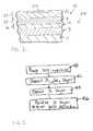
- FIG. 1is a schematic of the device of the present invention.
- FIG. 2is a flowchart of the method of the present invention.
- FIG. 1shows device 10 of the present invention.
- Device 10includes a silicon-on-insulator (SOI) substrate 12 prepared with a buried oxide (BOX) 13 , and a top-Si layer 14 being as thin as possible, typically having a thickness 16 of about 10-40 nM.
- SOIsilicon-on-insulator
- BOXburied oxide
- top-Si layer 14being as thin as possible, typically having a thickness 16 of about 10-40 nM.
- an epitaxial Si 1 ⁇ x Ge x film 18is deposited, with x being any value from 0.1 to 0.5 or higher, such as in a range of 0.1 to 0.9, if possible.
- the thickness 20 of film 18must be kept thin enough to avoid dislocation generation and/or propagation, i.e., to maintain the dislocation generation and/or propagation below a threshold value of 100/cm 2 .
- SIASemiconductor Industry Association
- Another way of determining the acceptable thickness of film 18is that the thickness must be kept thin enough to ensure a dislocation density no higher than that of the SOI Silicon starting substrate.
- Thickness 20typically ranges from 5 to 50 n.
- Another layer of epitaxial Si 22is then deposited on the SiGe layer.
- Layer 22has an appropriate thickness 24 , typically from 2 to 50 nm. Part of this last Si layer may be thermally oxidized to form a gate dielectric 26 for MOS applications.
- the SiGe and Si layers, 18 and 22 respectively,can be deposited by any of the standard epitaxial methods, such as low pressure chemical vapor deposition (LPCVD), ultra high vacuum chemical vapor deposition (UHVCVD), rapid thermal chemical vapor deposition (RTCVD), or molecular beam epitaxy (MBE).
- LPCVDlow pressure chemical vapor deposition
- UHVCVDultra high vacuum chemical vapor deposition
- RTCVDrapid thermal chemical vapor deposition
- MBEmolecular beam epitaxy
- the Si/SiGe layerscan be grown with either selective or non-selective chemistries on either patterned or un-patterned substrates.
- the “effective critical thickness”is the critical thickness for dislocation generation. Its increase depends on the amount of relaxation of the SiGe. Consequently, thicker SiGe layers or layers with higher Ge concentrations could be grown.
- the SiGe layermay have a Ge concentration of 0.3 or a thickness of 50 nm. Layers having higher concentrations of germanium would result in higher hole and electron mobilities. For example, accordingly to published experimental results, a device having a germanium concentration of 0.3 would have an field effective electron mobility of approximately 500 cm 2 /V-sec. Similarly, a device having a germanium concentration of 0.3 would have a field effective hole mobility of approximately 250 cm 2 /V-sec.
- the substrate silicon layer 14is tensily strained, the silicon germanium layer 18 is compressively strained, and the top silicon layer 22 is tensily strained.
- the explanation for the strain of the three layerscan be explained as follows. Silicon layer 14 is partially de-coupled from substrate 12 by buried oxide layer 13 . Accordingly, silicon layer 14 is somewhat free to relax when the SiGe layer 18 is grown on top of silicon layer 14 . If this happens to silicon layer 14 and SiGe layer 18 , then the silicon layer 22 grown on top of SiGe layer 18 will be tensily strained. In other words, by growing SiGe layer 18 on the SOI, the strain will be shared between SiGe layer 18 and substrate silicon layer 14 .
- SiGe layerbeing compressively strained, but partially relaxed.
- Substrate silicon layer 14will be tensily strained.
- the additional silicon cap layer 22is grown on SiGe layer 18 wherein cap layer 22 will be tensily strained.
- the silicon cap layer 22can be used as a channel.
- the silicon cap layer 22 or the SiGe layer 18can be used as a channel.
- FIG. 2shows a flowchart of the process steps of the present invention.
- Step 40comprises providing a silicon-on-insulator substrate having a silicon layer therein.
- Step 42comprises depositing a SiGe layer on the silicon-on-insulator substrate.
- Step 44comprises depositing a silicon layer on the SiGe layer.
- Step 46comprises oxidizing a section of the top silicon layer to form a gate dielectric.
- the processresults in a layered structure 28 having a partially relaxed, compressively strained SiGe layer and tensily strained Si layers having low dislocation densities.
- the layered structurealso provides enhanced hole and electron mobilities.
Landscapes
- Thin Film Transistor (AREA)
- Metal-Oxide And Bipolar Metal-Oxide Semiconductor Integrated Circuits (AREA)
- Recrystallisation Techniques (AREA)
- Insulated Gate Type Field-Effect Transistor (AREA)
Abstract
Description
- This invention relates to enhanced NMOS and PMOS transistors using strained Si/SiGe layers on silicon-on-insulator substrates and, more particularly, to NMOS and PMOS transistors including compressively strained, but partially relaxed, SiGe and tensily strained Si layers having low dislocation densities.[0001]
- During the past decade a number of different device structures based on silicon germanium (SiGe) technology were developed to produce field effect transistors (FET) with enhanced mobilities. One design for a p-channel metal oxide semiconductor (PMOS) transistor includes a buried, pseudomorphically strained SiGe layer capped by an unstrained silicon (Si) layer. The silicon cap layer is partially oxidized to form a gate dielectric. Due to an offset in the valence band, the holes can be confined to the SiGe channel. This enhances the mobility in two ways: by the intrinsic properties of the strained SiGe layer; and, by separating the holes from the silicon dioxide/silicon (SiO[0002]2/Si) interface, thereby reducing surface scattering. In this design, dislocations in the SiGe film can be avoided if the SiGe film thickness is made very thin. Fabrication of this device is compatible with state-of-the art complementary metal oxide semiconductor (CMOS) processing. However, since there is virtually no offset between the Si film and the strained SiGe film at the conduction band, this design offers no advantage for n-channel metal oxide semiconductor (NMOS) devices and may actually worsen performance.
- Compressively strained SiGe and tensily strained Si films can be used to make p-channel modulation doped field effect transistor (p-MODFET) and n-channel modulation doped field effect transistor (n-MODFET) devices with greatly enhanced hole and electron mobilities, respectively. However, these designs require graded, relaxed SiGe buffer layers as “virtual” substrates. The dislocation densities in these buffers are seven orders of magnitude too high for large-scale production feasibility.[0003]
- Pseudomorphic SiGe PMOS devices have been proposed and fabricated on SOI material, giving significantly enhanced hole mobilities. In two separate fabricated devices, the top Si layer of the SOI substrate has been quite thick, 150 nm and 50 nm, respectively.[0004]
- Accordingly, there is a need for a device that provides both compressively strained SiGe and tensily strained Si layers without the high dislocation densities found in graded, relaxed SiGe buffer layers. If such a device could be fabricated, then both hole and electron mobilities could be enhanced.[0005]
- Below the “critical thickness” for dislocation generation and propagation, SiGe layers can be grown “pseudomorphically” to a bulk Si substrate. This means the layer is epitaxially strained to the substrate. Any Si then grown on top of this SiGe layer is consequently relaxed, with no strain. However, if the SiGe could be grown on an extremely thin Si substrate, of a thickness comparable to the SiGe layer, both the SiGe layer and Si layer would be strained, without dislocations. Essentially, the total strain would be shared between the SiGe and the Si layers. Another effect would be that the SiGe critical thickness would be increased. Additionally, a Si layer grown on top of the SiGe would be tensily strained.[0006]
- The closest thing available to such a thin Si substrate is the top Si layer in a silicon-on-insulator (SOI) substrate. The increased defect density of SOI substrates, compared to bulk silicon substrates, may promote strain relaxation. It may then be expected that when growing a thin Si/SiGe stack on top of an equally thin top Si layer of a SOI substrate that the SiGe will be compressively strained and the Si layers will be tensily strained, without high dislocation densities.[0007]
- Accordingly, the present invention comprises a thin Si/SiGe stack on top of an equally thin top Si layer of a SOI substrate. The SiGe layer is compressively strained, but partially relaxed, and the Si layers are each tensily strained, without high dislocation densities. The silicon layer of the SOI substrate has a thickness of approximately 10 to 40 nm. The SiGe layer has a thickness of approximately 5 to 50 nm. The top, second Si layer has a thickness of approximately 2 to 50 nm.[0008]
- Accordingly, an object of the invention is to provide enhanced NMOS and PMOS transistors using strained Si/SiGe layers on silicon-on-insulator substrates.[0009]
- Another object of the invention is to provide enhanced NMOS and PMOS transistors including compressively strained SiGe and tensily strained Si layers having low dislocation densities.[0010]
- A further object of the invention is to provide enhanced NMOS and PMOS transistors having enhanced hole and electron mobilities.[0011]
- FIG. 1 is a schematic of the device of the present invention.[0012]
- FIG. 2 is a flowchart of the method of the present invention.[0013]
- FIG. 1 shows[0014]
device 10 of the present invention.Device 10 includes a silicon-on-insulator (SOI)substrate 12 prepared with a buried oxide (BOX)13, and a top-Si layer 14 being as thin as possible, typically having a thickness 16 of about 10-40 nM. Next, an epitaxial Si1−xGexfilm 18 is deposited, with x being any value from 0.1 to 0.5 or higher, such as in a range of 0.1 to 0.9, if possible. The thickness20 offilm 18 must be kept thin enough to avoid dislocation generation and/or propagation, i.e., to maintain the dislocation generation and/or propagation below a threshold value of 100/cm2. Those skilled in the art will understand that this value depends on the recommended Semiconductor Industry Association (SIA) values, which vary for each generation of device. Another way of determining the acceptable thickness offilm 18 is that the thickness must be kept thin enough to ensure a dislocation density no higher than that of the SOI Silicon starting substrate. Thickness20 typically ranges from 5 to 50 n. Another layer ofepitaxial Si 22 is then deposited on the SiGe layer.Layer 22 has anappropriate thickness 24, typically from 2 to 50 nm. Part of this last Si layer may be thermally oxidized to form a gate dielectric26 for MOS applications. - The SiGe and Si layers,[0015]18 and22 respectively, can be deposited by any of the standard epitaxial methods, such as low pressure chemical vapor deposition (LPCVD), ultra high vacuum chemical vapor deposition (UHVCVD), rapid thermal chemical vapor deposition (RTCVD), or molecular beam epitaxy (MBE). The Si/SiGe layers can be grown with either selective or non-selective chemistries on either patterned or un-patterned substrates.
- Both the sharing of strain between[0016]
SiGe layer 18 andsubstrate Si layer 14, and the capping ofSiGe layer 18 withSi layer 22, increases the effective critical thickness of theentire stack 28. The “effective critical thickness” is the critical thickness for dislocation generation. Its increase depends on the amount of relaxation of the SiGe. Consequently, thicker SiGe layers or layers with higher Ge concentrations could be grown. For example, the SiGe layer may have a Ge concentration of 0.3 or a thickness of 50 nm. Layers having higher concentrations of germanium would result in higher hole and electron mobilities. For example, accordingly to published experimental results, a device having a germanium concentration of 0.3 would have an field effective electron mobility of approximately 500 cm2/V-sec. Similarly, a device having a germanium concentration of 0.3 would have a field effective hole mobility of approximately 250 cm2/V-sec. - Due to the thicknesses of the deposited layers, the[0017]
substrate silicon layer 14 is tensily strained, thesilicon germanium layer 18 is compressively strained, and thetop silicon layer 22 is tensily strained. The explanation for the strain of the three layers can be explained as follows.Silicon layer 14 is partially de-coupled fromsubstrate 12 by buriedoxide layer 13. Accordingly,silicon layer 14 is somewhat free to relax when the SiGelayer 18 is grown on top ofsilicon layer 14. If this happens tosilicon layer 14 andSiGe layer 18, then thesilicon layer 22 grown on top ofSiGe layer 18 will be tensily strained. In other words, by growingSiGe layer 18 on the SOI, the strain will be shared betweenSiGe layer 18 andsubstrate silicon layer 14. This will result in the SiGe layer being compressively strained, but partially relaxed.Substrate silicon layer 14 will be tensily strained. Then, the additionalsilicon cap layer 22 is grown onSiGe layer 18 whereincap layer 22 will be tensily strained. In NMOS devices, thesilicon cap layer 22 can be used as a channel. In PMOS devices, thesilicon cap layer 22 or theSiGe layer 18 can be used as a channel. - FIG. 2 shows a flowchart of the process steps of the present invention.[0018]
Step 40 comprises providing a silicon-on-insulator substrate having a silicon layer therein.Step 42 comprises depositing a SiGe layer on the silicon-on-insulator substrate. Step44 comprises depositing a silicon layer on the SiGe layer. Step46 comprises oxidizing a section of the top silicon layer to form a gate dielectric. The process results in alayered structure 28 having a partially relaxed, compressively strained SiGe layer and tensily strained Si layers having low dislocation densities. The layered structure also provides enhanced hole and electron mobilities. - The same or very similar structures could be used for both n-channel and p-channel devices, with the[0019]
last Si layer 22 acting as the channel for electrons and theSiGe layer 18 acting as the channel for holes.Silicon cap layer 22 could also be used as the channel for both electrons or holes. Either CMOS or MODFET designs could be used. Moreover, the structure and fabrication processes are compatible with those of standard CMOS structures and fabrication steps. Alternatively, silicon germanium carbon (SiGeC) layers may also be used as part of this structure. - Thus, a transistor using strained Si/SiGe layers on a silicon-on-insulator substrate, and a method of fabricating the same, has been disclosed. Although preferred structures and methods of fabricating the device have been disclosed, it should be appreciated that further variations and modifications may be made thereto without departing from the scope of the invention as defined in the appended claims.[0020]
Claims (21)
1. A metal oxide semiconductor transistor comprising:
a silicon-on-insulator substrate including a substrate silicon layer therein;
a silicon germanium layer positioned on said substrate silicon layer; and
a top silicon layer positioned on said silicon germanium layer, wherein said silicon germanium layer is compressively strained and said top silicon layer and said substrate silicon layer are both tensily strained,
wherein said substrate silicon layer has a thickness in a range of 10 to 40 nm.
2. The transistor ofclaim 1 wherein said transistor has a dislocation density no greater than a dislocation density of the substrate silicon layer.
3. The transistor ofclaim 1 wherein said silicon germanium layer has a thickness in a range of 5 to 50 nm.
4. The transistor ofclaim 1 wherein said silicon germanium layer comprises Si1−xGex, wherein x is in a range of 0.1 to 0.9.
5. The transistor ofclaim 1 wherein said silicon germanium layer comprises Si1−xGex, wherein x is in a range of 0.1 to 0.5.
6. The transistor ofclaim 1 wherein said top silicon layer has a thickness in a range of 2 to 50 nm.
7. The transistor ofclaim 1 wherein said top silicon layer includes a gate dielectric region.
8. The transistor ofclaim 1 wherein said transistor has a field effective electron mobility of at least 500 cm2/V-sec.
9. A metal oxide semiconductor transistor comprising:
a silicon-on-insulator substrate including a substrate silicon layer therein;
a silicon germanium layer positioned on said substrate silicon layer; and
a top silicon layer positioned on said silicon germanium layer, wherein said substrate silicon layer has a thickness in a range of 10 to 40 nm, said silicon germanium layer has a thickness in a range of 5 to 50 nm, and said top silicon layer has a thickness in a range of 2 to 50 nm.
10. The transistor ofclaim 9 wherein said silicon germanium layer comprises Si1−xGex, wherein x is in a range of 0.1 to 0.5.
11. The transistor ofclaim 9 wherein said top silicon layer includes a gate dielectric region.
12. The transistor ofclaim 9 wherein said transistor has a field effective electron mobility of at least 500 cm2/V-sec.
13. The transistor ofclaim 9 wherein said silicon germanium layer is partially relaxed and compressively strained and said top silicon layer and said substrate silicon layer are both tensily strained.
14. The transistor ofclaim 9 wherein said transistor comprises a NMOS transistor.
15. The transistor ofclaim 9 wherein said transistor comprises a PMOS transistor.
16. A method of fabricating a transistor having enhanced mobility, comprising the steps of:
providing a silicon-on-insulator substrate including a substrate silicon layer having a thickness in a range of 10 to 40 nm;
depositing a silicon germanium layer on said substrate silicon layer, wherein said silicon germanium layer has a thickness in a range of 5 to 50 nm; and
depositing a top silicon layer on said silicon germanium layer, wherein said top silicon layer has a thickness in a range of 2 to 50 nm.
17. The method ofclaim 16 wherein said silicon germanium layer is deposited so as to be compressively strained, and said top silicon layer and said substrate silicon layer are deposited so as to both be tensily strained.
18. The method ofclaim 16 wherein said silicon germanium layer comprises Si1−xGex, and wherein x is in a range of 0.1 to 0.9.
19. The method ofclaim 16 further comprising forming a gate dielectric region in said top silicon layer.
20. The method ofclaim 16 wherein said method produces a transistor having a field effective electron mobility of at least 500 cm2/V-sec, and a dislocation density no greater than a dislocation density of the substrate silicon layer initially provided.
21. The transistor ofclaim 1 wherein said transistor has a field effective hole mobility of at least 250 cm2/V-sec.
Priority Applications (6)
| Application Number | Priority Date | Filing Date | Title |
|---|---|---|---|
| US09/855,392US20020167048A1 (en) | 2001-05-14 | 2001-05-14 | Enhanced mobility NMOS and PMOS transistors using strained Si/SiGe layers on silicon-on-insulator substrates |
| US10/016,373US20020168802A1 (en) | 2001-05-14 | 2001-10-30 | SiGe/SOI CMOS and method of making the same |
| JP2002127359AJP2002368230A (en) | 2001-05-14 | 2002-04-26 | NMOS and PMOS transistors with good mobility using strained Si / SiGe layers on a silicon-on-insulator substrate |
| TW091109583ATW564467B (en) | 2001-05-14 | 2002-05-08 | Enhanced mobility NMOS and PMOS transistors using strained Si/SiGe layers on silicon-on-insulator substrates |
| KR10-2002-0026453AKR100501849B1 (en) | 2001-05-14 | 2002-05-14 | ENHANCED MOBILITY NMOS AND PMOS TRANSISTORS USING STRAINED Si/SiGe LAYERS ON SILICON-ON-INSULATOR SUBSTRATES |
| CNB021401055ACN1208838C (en) | 2001-05-14 | 2002-05-14 | Mobility-enhanced transistors with strained Si/SiGe layers |
Applications Claiming Priority (1)
| Application Number | Priority Date | Filing Date | Title |
|---|---|---|---|
| US09/855,392US20020167048A1 (en) | 2001-05-14 | 2001-05-14 | Enhanced mobility NMOS and PMOS transistors using strained Si/SiGe layers on silicon-on-insulator substrates |
Related Child Applications (1)
| Application Number | Title | Priority Date | Filing Date |
|---|---|---|---|
| US10/016,373Continuation-In-PartUS20020168802A1 (en) | 2001-05-14 | 2001-10-30 | SiGe/SOI CMOS and method of making the same |
Publications (1)
| Publication Number | Publication Date |
|---|---|
| US20020167048A1true US20020167048A1 (en) | 2002-11-14 |
Family
ID=25321139
Family Applications (1)
| Application Number | Title | Priority Date | Filing Date |
|---|---|---|---|
| US09/855,392AbandonedUS20020167048A1 (en) | 2001-05-14 | 2001-05-14 | Enhanced mobility NMOS and PMOS transistors using strained Si/SiGe layers on silicon-on-insulator substrates |
Country Status (5)
| Country | Link |
|---|---|
| US (1) | US20020167048A1 (en) |
| JP (1) | JP2002368230A (en) |
| KR (1) | KR100501849B1 (en) |
| CN (1) | CN1208838C (en) |
| TW (1) | TW564467B (en) |
Cited By (22)
| Publication number | Priority date | Publication date | Assignee | Title |
|---|---|---|---|---|
| US20030052334A1 (en)* | 2001-06-18 | 2003-03-20 | Lee Minjoo L. | Structure and method for a high-speed semiconductor device |
| US20040147079A1 (en)* | 2002-06-10 | 2004-07-29 | Leonard Forbes | Output prediction logic circuits with ultra-thin vertical transistors and methods of formation |
| US20040159834A1 (en)* | 2003-02-13 | 2004-08-19 | Taiwan Semiconductor Manufacturing Co., Ltd. | Strained silicon layer semiconductor product employing strained insulator layer |
| US20040253774A1 (en)* | 2003-06-16 | 2004-12-16 | Boyan Boyanov | Double-gate transistor with enhanced carrier mobility |
| US20050070070A1 (en)* | 2003-09-29 | 2005-03-31 | International Business Machines | Method of forming strained silicon on insulator |
| US20050151164A1 (en)* | 2001-06-21 | 2005-07-14 | Amberwave Systems Corporation | Enhancement of p-type metal-oxide-semiconductor field effect transistors |
| US20050170104A1 (en)* | 2004-01-29 | 2005-08-04 | Applied Materials, Inc. | Stress-tuned, single-layer silicon nitride film |
| US20050221550A1 (en)* | 2001-08-09 | 2005-10-06 | Amberwave Systems Corporation | Dual layer semiconductor devices |
| US20060001088A1 (en)* | 2004-07-01 | 2006-01-05 | International Business Machines Corporation | Strained Si MOSFET on tensile-strained SiGe-on-insulator (SGOI) |
| US20060113603A1 (en)* | 2004-12-01 | 2006-06-01 | Amberwave Systems Corporation | Hybrid semiconductor-on-insulator structures and related methods |
| US7074623B2 (en)* | 2002-06-07 | 2006-07-11 | Amberwave Systems Corporation | Methods of forming strained-semiconductor-on-insulator finFET device structures |
| US7227176B2 (en) | 1998-04-10 | 2007-06-05 | Massachusetts Institute Of Technology | Etch stop layer system |
| US7232743B2 (en) | 2003-01-29 | 2007-06-19 | S.O.I.Tec Silicon On Insulator Technologies S.A. | Semiconductor structure for providing strained crystalline layer on insulator and method for fabricating same |
| US7259388B2 (en) | 2002-06-07 | 2007-08-21 | Amberwave Systems Corporation | Strained-semiconductor-on-insulator device structures |
| US7348259B2 (en) | 2001-04-04 | 2008-03-25 | Massachusetts Institute Of Technology | Method of fabricating a semiconductor structure that includes transferring one or more material layers to a substrate and smoothing an exposed surface of at least one of the material layers |
| CN100385634C (en)* | 2003-10-22 | 2008-04-30 | 国际商业机器公司 | Method for fabricating thin SOI CMOS with recessed channel and device fabricated therefor |
| US7393733B2 (en) | 2004-12-01 | 2008-07-01 | Amberwave Systems Corporation | Methods of forming hybrid fin field-effect transistor structures |
| US7566606B2 (en) | 2002-06-07 | 2009-07-28 | Amberwave Systems Corporation | Methods of fabricating semiconductor devices having strained dual channel layers |
| US20100301455A1 (en)* | 2007-11-27 | 2010-12-02 | Shin-Etsu Chemical Co., Ltd. | Method for producing a bonded substrate |
| US8748292B2 (en) | 2002-06-07 | 2014-06-10 | Taiwan Semiconductor Manufacturing Company, Ltd. | Methods of forming strained-semiconductor-on-insulator device structures |
| US8828851B2 (en)* | 2012-02-01 | 2014-09-09 | Stmicroeletronics, Inc. | Method to enable the formation of silicon germanium channel of FDSOI devices for PFET threshold voltage engineering |
| US10515801B2 (en) | 2007-06-04 | 2019-12-24 | Micron Technology, Inc. | Pitch multiplication using self-assembling materials |
Families Citing this family (10)
| Publication number | Priority date | Publication date | Assignee | Title |
|---|---|---|---|---|
| JP4304976B2 (en) | 2002-12-19 | 2009-07-29 | 東ソー株式会社 | Detection method of acid-fast bacteria targeting ribosomal RNA |
| CN100544022C (en)* | 2004-01-07 | 2009-09-23 | 国际商业机器公司 | Semiconductor material having a <110> crystal oriented silicon-containing layer and method of forming the same |
| JP4177775B2 (en)* | 2004-03-16 | 2008-11-05 | 株式会社東芝 | Semiconductor substrate, manufacturing method thereof, and semiconductor device |
| US7223994B2 (en)* | 2004-06-03 | 2007-05-29 | International Business Machines Corporation | Strained Si on multiple materials for bulk or SOI substrates |
| US7187059B2 (en)* | 2004-06-24 | 2007-03-06 | International Business Machines Corporation | Compressive SiGe <110> growth and structure of MOSFET devices |
| US20060011906A1 (en)* | 2004-07-14 | 2006-01-19 | International Business Machines Corporation | Ion implantation for suppression of defects in annealed SiGe layers |
| US7235812B2 (en)* | 2004-09-13 | 2007-06-26 | International Business Machines Corporation | Method of creating defect free high Ge content (>25%) SiGe-on-insulator (SGOI) substrates using wafer bonding techniques |
| US7238589B2 (en)* | 2004-11-01 | 2007-07-03 | International Business Machines Corporation | In-place bonding of microstructures |
| KR100592749B1 (en) | 2004-11-17 | 2006-06-26 | 한국전자통신연구원 | High-voltage field effect transistor having a heterogeneous structure of silicon and silicon germanium and a method of manufacturing the same |
| CN1808268B (en)* | 2005-01-18 | 2010-10-06 | 中芯国际集成电路制造(上海)有限公司 | Metal hard mask method and structure for strained silicon MOS transistor |
Family Cites Families (3)
| Publication number | Priority date | Publication date | Assignee | Title |
|---|---|---|---|---|
| US5461243A (en)* | 1993-10-29 | 1995-10-24 | International Business Machines Corporation | Substrate for tensilely strained semiconductor |
| DE19720008A1 (en)* | 1997-05-13 | 1998-11-19 | Siemens Ag | Integrated CMOS circuit arrangement and method for its production |
| KR100232320B1 (en)* | 1997-07-15 | 1999-12-01 | 포만 제프리 엘 | Enhanced mobility p-channel structure in silicon on insulator |
- 2001
- 2001-05-14USUS09/855,392patent/US20020167048A1/ennot_activeAbandoned
- 2002
- 2002-04-26JPJP2002127359Apatent/JP2002368230A/ennot_activeWithdrawn
- 2002-05-08TWTW091109583Apatent/TW564467B/ennot_activeIP Right Cessation
- 2002-05-14KRKR10-2002-0026453Apatent/KR100501849B1/ennot_activeExpired - Fee Related
- 2002-05-14CNCNB021401055Apatent/CN1208838C/ennot_activeExpired - Fee Related
Cited By (47)
| Publication number | Priority date | Publication date | Assignee | Title |
|---|---|---|---|---|
| US7227176B2 (en) | 1998-04-10 | 2007-06-05 | Massachusetts Institute Of Technology | Etch stop layer system |
| US7348259B2 (en) | 2001-04-04 | 2008-03-25 | Massachusetts Institute Of Technology | Method of fabricating a semiconductor structure that includes transferring one or more material layers to a substrate and smoothing an exposed surface of at least one of the material layers |
| US20080128747A1 (en)* | 2001-06-18 | 2008-06-05 | Lee Minjoo L | STRUCTURE AND METHOD FOR A HIGH-SPEED SEMICONDUCTOR DEVICE HAVING A Ge CHANNEL LAYER |
| US7301180B2 (en) | 2001-06-18 | 2007-11-27 | Massachusetts Institute Of Technology | Structure and method for a high-speed semiconductor device having a Ge channel layer |
| US8436336B2 (en) | 2001-06-18 | 2013-05-07 | Massachusetts Institute Of Technology | Structure and method for a high-speed semiconductor device having a Ge channel layer |
| US20030052334A1 (en)* | 2001-06-18 | 2003-03-20 | Lee Minjoo L. | Structure and method for a high-speed semiconductor device |
| US20050151164A1 (en)* | 2001-06-21 | 2005-07-14 | Amberwave Systems Corporation | Enhancement of p-type metal-oxide-semiconductor field effect transistors |
| US20050221550A1 (en)* | 2001-08-09 | 2005-10-06 | Amberwave Systems Corporation | Dual layer semiconductor devices |
| US7465619B2 (en)* | 2001-08-09 | 2008-12-16 | Amberwave Systems Corporation | Methods of fabricating dual layer semiconductor devices |
| US7259388B2 (en) | 2002-06-07 | 2007-08-21 | Amberwave Systems Corporation | Strained-semiconductor-on-insulator device structures |
| US7838392B2 (en) | 2002-06-07 | 2010-11-23 | Taiwan Semiconductor Manufacturing Company, Ltd. | Methods for forming III-V semiconductor device structures |
| US7420201B2 (en) | 2002-06-07 | 2008-09-02 | Amberwave Systems Corporation | Strained-semiconductor-on-insulator device structures with elevated source/drain regions |
| US7414259B2 (en) | 2002-06-07 | 2008-08-19 | Amberwave Systems Corporation | Strained germanium-on-insulator device structures |
| US8748292B2 (en) | 2002-06-07 | 2014-06-10 | Taiwan Semiconductor Manufacturing Company, Ltd. | Methods of forming strained-semiconductor-on-insulator device structures |
| US7074623B2 (en)* | 2002-06-07 | 2006-07-11 | Amberwave Systems Corporation | Methods of forming strained-semiconductor-on-insulator finFET device structures |
| US7109516B2 (en) | 2002-06-07 | 2006-09-19 | Amberwave Systems Corporation | Strained-semiconductor-on-insulator finFET device structures |
| US7566606B2 (en) | 2002-06-07 | 2009-07-28 | Amberwave Systems Corporation | Methods of fabricating semiconductor devices having strained dual channel layers |
| US7588994B2 (en) | 2002-06-07 | 2009-09-15 | Amberwave Systems Corporation | Methods for forming strained-semiconductor-on-insulator device structures by mechanically inducing strain |
| US7297612B2 (en) | 2002-06-07 | 2007-11-20 | Amberwave Systems Corporation | Methods for forming strained-semiconductor-on-insulator device structures by use of cleave planes |
| US20050156230A1 (en)* | 2002-06-10 | 2005-07-21 | Leonard Forbes | Output prediction logic circuits with ultra-thin vertical transistors and methods of formation |
| US20040147079A1 (en)* | 2002-06-10 | 2004-07-29 | Leonard Forbes | Output prediction logic circuits with ultra-thin vertical transistors and methods of formation |
| US7217974B2 (en) | 2002-06-10 | 2007-05-15 | Micron Technology, Inc. | Output prediction logic circuits with ultra-thin vertical transistors and methods of formation |
| US6998311B2 (en)* | 2002-06-10 | 2006-02-14 | Micron Technology, Inc. | Methods of forming output prediction logic circuits with ultra-thin vertical transistors |
| US7232743B2 (en) | 2003-01-29 | 2007-06-19 | S.O.I.Tec Silicon On Insulator Technologies S.A. | Semiconductor structure for providing strained crystalline layer on insulator and method for fabricating same |
| US6924181B2 (en)* | 2003-02-13 | 2005-08-02 | Taiwan Semiconductor Manufacturing Co., Ltd | Strained silicon layer semiconductor product employing strained insulator layer |
| US20040159834A1 (en)* | 2003-02-13 | 2004-08-19 | Taiwan Semiconductor Manufacturing Co., Ltd. | Strained silicon layer semiconductor product employing strained insulator layer |
| US6974733B2 (en) | 2003-06-16 | 2005-12-13 | Intel Corporation | Double-gate transistor with enhanced carrier mobility |
| US20040253774A1 (en)* | 2003-06-16 | 2004-12-16 | Boyan Boyanov | Double-gate transistor with enhanced carrier mobility |
| US20050070070A1 (en)* | 2003-09-29 | 2005-03-31 | International Business Machines | Method of forming strained silicon on insulator |
| CN100385634C (en)* | 2003-10-22 | 2008-04-30 | 国际商业机器公司 | Method for fabricating thin SOI CMOS with recessed channel and device fabricated therefor |
| US20050170104A1 (en)* | 2004-01-29 | 2005-08-04 | Applied Materials, Inc. | Stress-tuned, single-layer silicon nitride film |
| US20060001088A1 (en)* | 2004-07-01 | 2006-01-05 | International Business Machines Corporation | Strained Si MOSFET on tensile-strained SiGe-on-insulator (SGOI) |
| US8017499B2 (en) | 2004-07-01 | 2011-09-13 | International Business Machines Corporation | Strained Si MOSFET on tensile-strained SiGe-on-insulator (SGOI) |
| US7485518B2 (en) | 2004-07-01 | 2009-02-03 | International Business Machines Corporation | Strained Si MOSFET on tensile-strained SiGe-on-insulator (SGOI) |
| US7507989B2 (en) | 2004-07-01 | 2009-03-24 | International Business Machines Corporation | Strained Si MOSFET on tensile-strained SiGe-on-insulator (SGOI) |
| US7217949B2 (en)* | 2004-07-01 | 2007-05-15 | International Business Machines Corporation | Strained Si MOSFET on tensile-strained SiGe-on-insulator (SGOI) |
| US20080042166A1 (en)* | 2004-07-01 | 2008-02-21 | International Business Machines Corporation | STRAINED Si MOSFET ON TENSILE-STRAINED SiGe-ON-INSULATOR (SGOI) |
| US20070155130A1 (en)* | 2004-07-01 | 2007-07-05 | International Business Machines Corporation | STRAINED Si MOSFET ON TENSILE-STRAINED SiGe-ON-INSULATOR (SGOI) |
| US20080220588A1 (en)* | 2004-07-01 | 2008-09-11 | International Business Machines Corporation | STRAINED Si MOSFET ON TENSILE-STRAINED SiGe-ON-INSULATOR (SGOI) |
| US8183627B2 (en) | 2004-12-01 | 2012-05-22 | Taiwan Semiconductor Manufacturing Company, Ltd. | Hybrid fin field-effect transistor structures and related methods |
| US7393733B2 (en) | 2004-12-01 | 2008-07-01 | Amberwave Systems Corporation | Methods of forming hybrid fin field-effect transistor structures |
| US20060113603A1 (en)* | 2004-12-01 | 2006-06-01 | Amberwave Systems Corporation | Hybrid semiconductor-on-insulator structures and related methods |
| US10515801B2 (en) | 2007-06-04 | 2019-12-24 | Micron Technology, Inc. | Pitch multiplication using self-assembling materials |
| EP2216803A4 (en)* | 2007-11-27 | 2011-08-10 | Shinetsu Chemical Co | METHOD FOR MANUFACTURING LAMINATED SUBSTRATE |
| US20100301455A1 (en)* | 2007-11-27 | 2010-12-02 | Shin-Etsu Chemical Co., Ltd. | Method for producing a bonded substrate |
| US8716106B2 (en) | 2007-11-27 | 2014-05-06 | Shin-Etsu Chemical Co., Ltd. | Method for producing a bonded substrate |
| US8828851B2 (en)* | 2012-02-01 | 2014-09-09 | Stmicroeletronics, Inc. | Method to enable the formation of silicon germanium channel of FDSOI devices for PFET threshold voltage engineering |
Also Published As
| Publication number | Publication date |
|---|---|
| CN1208838C (en) | 2005-06-29 |
| CN1388589A (en) | 2003-01-01 |
| JP2002368230A (en) | 2002-12-20 |
| TW564467B (en) | 2003-12-01 |
| KR20020088057A (en) | 2002-11-25 |
| KR100501849B1 (en) | 2005-07-20 |
Similar Documents
| Publication | Publication Date | Title |
|---|---|---|
| US20020167048A1 (en) | Enhanced mobility NMOS and PMOS transistors using strained Si/SiGe layers on silicon-on-insulator substrates | |
| US9711413B2 (en) | High performance CMOS device design | |
| JP3974329B2 (en) | Layered structure for forming Ge channel field effect transistors | |
| US8304810B2 (en) | Semiconductor device and semiconductor substrate having selectively etched portions filled with silicon germanium | |
| US6974735B2 (en) | Dual layer Semiconductor Devices | |
| US6900502B2 (en) | Strained channel on insulator device | |
| US7569869B2 (en) | Transistor having tensile strained channel and system including same | |
| CN100481490C (en) | Integration of strained Ge in advanced CMOS technologies | |
| US7335929B2 (en) | Transistor with a strained region and method of manufacture | |
| US7098057B2 (en) | Ultra high-speed Si/SiGe modulation-doped field effect transistors on ultra thin SOI/SGOI substrate | |
| US7791107B2 (en) | Strained tri-channel layer for semiconductor-based electronic devices | |
| US20030162335A1 (en) | Semiconductor device and method for fabricating the same | |
| US20040007715A1 (en) | Heterojunction field effect transistors using silicon-germanium and silicon-carbon alloys | |
| US20080179636A1 (en) | N-fets with tensilely strained semiconductor channels, and method for fabricating same using buried pseudomorphic layers | |
| JPH07321222A (en) | CMOS transistor logic circuit using strained Si / SiGe heterostructure layer | |
| US6949761B2 (en) | Structure for and method of fabricating a high-mobility field-effect transistor | |
| US20050274978A1 (en) | Single metal gate material CMOS using strained si-silicon germanium heterojunction layered substrate | |
| WO2003015160A2 (en) | Dual layer cmos devices | |
| Banerjee | SiGe-Channel HFETs | |
| Takagi | High performance CMOS device technologies in nano CMOS era |
Legal Events
| Date | Code | Title | Description |
|---|---|---|---|
| AS | Assignment | Owner name:SHARP LABORATORIES OF AMERICA, INC., WASHINGTON Free format text:ASSIGNMENT OF ASSIGNORS INTEREST;ASSIGNORS:TWEET, DOUGLAS J.;HSU, SHENG TENG;REEL/FRAME:011815/0345 Effective date:20010514 | |
| STCB | Information on status: application discontinuation | Free format text:ABANDONED -- FAILURE TO RESPOND TO AN OFFICE ACTION |