US20020163350A1 - Substrate-holding device for testing circuit arrangements on substrates - Google Patents
Substrate-holding device for testing circuit arrangements on substratesDownload PDFInfo
- Publication number
- US20020163350A1 US20020163350A1US10/139,735US13973502AUS2002163350A1US 20020163350 A1US20020163350 A1US 20020163350A1US 13973502 AUS13973502 AUS 13973502AUS 2002163350 A1US2002163350 A1US 2002163350A1
- Authority
- US
- United States
- Prior art keywords
- layer
- substrate
- holding
- region
- substrate according
- Prior art date
- Legal status (The legal status is an assumption and is not a legal conclusion. Google has not performed a legal analysis and makes no representation as to the accuracy of the status listed.)
- Granted
Links
Images


Classifications
- G—PHYSICS
- G01—MEASURING; TESTING
- G01R—MEASURING ELECTRIC VARIABLES; MEASURING MAGNETIC VARIABLES
- G01R1/00—Details of instruments or arrangements of the types included in groups G01R5/00 - G01R13/00 and G01R31/00
- G01R1/02—General constructional details
- G01R1/04—Housings; Supporting members; Arrangements of terminals
- G01R1/0408—Test fixtures or contact fields; Connectors or connecting adaptors; Test clips; Test sockets
Definitions
- the inventionrelates to a substrate-holding device for probes for testing circuit arrangements on substrates and more particularly to a monolithic substrate-holding device.
- a substrate holder of the type mentioned at the beginningis described in U.S. Pat. No. 5,457,398. It has first and second elements that are electrically insulated from one another, the first element of the substrate holder having an upper surface for the horizontal accommodation of a test circuit for testing by an electric probe.
- the substrate holderis surrounded by a sheath.
- This arrangementis provided for a triaxial structure.
- the second elementhas upper and lower parts, each of which consists of conductive material.
- the first elementcarries a force potential
- the second elementcarries a guard potential
- the sheathcarries a shield potential.
- U.S. Pat. No. 5,610,529discloses a structure of a substrate holder that has an electrically conductive holding plate. This holding plate adjoins an insulating plate. Below the insulating plate, there is provided a so-called thermochuck, which provides for the addition or removal of energy to or from the substrate, depending on whether it is to be tested at high or low temperatures.
- thermochuckaddition or removal of thermal energy may be effected conventionally or alternatively by gases or liquids controlled externally and conveyed through the thermochuck, as described in U.S. Pat. Nos. 4,426,619 and 4,734,872.
- the holding platecarries a force potential and the thermochuck a guard potential.
- an object of the inventionis to improve the homogeneity of thermal conduction to the substrate and increase the accuracy of measurement.
- the substrate-holding deviceis designed as a one-piece ceramic element having variably heavily doped layers. Owing to the one-piece nature of the ceramic element, opposing surfaces defining the interface between layers in the multipart structure according to the prior art, are avoided. This causes a reduction in the influence of the tribolectric effect.
- material propertiesmay be adjusted so that they satisfy the technical requirements of conductivity, resistivity and the like. For example, the impedance level of the arrangement is therefore adjustable.
- a ceramic elementis doped to provide a first layer region at least partially enclosing the surface that has a high electrical conductivity less than 10 ⁇ 1 to 10 ⁇ 3 ⁇ cm.
- the ceramic elementalso includes a second layer region located under the first layer region which exhibits an insulating resistance greater than 10 10 to 10 12 ⁇ and a third layer region located thereunder which is doped to provide a high electrical conductivity less than 10 ⁇ 1 to 10 ⁇ 3 ⁇ cm.
- the first layeris provided with an external contact connection for connection of a force potential and the third layer with an external contact connection for connection to a guard potential.
- the substrate to be testedis placeable on the first layer, which has a conductive layer.
- This first layerserves for a carrying force potential.
- a first insulating layer at least partially enclosing the surfacehas an insulating resistance greater than 10 10 to 10 12 ⁇
- This embodimentmakes it possible to perform HF measurements on substrates.
- the first insulating layer with the absorption layerresults in an impedance level that is adjustable according to the insulating or dielectric properties of the first insulating layer and the conductivity of the absorption layer.
- the substratehas under the third layer a fourth layer with a great insulating resistance.
- This fourth layerserves for insulation of the third layer downward. This may be advantageous in order to arrange additional layers under the third layer or in order to place the arrangement on a conductive element.
- the substrate-holding deviceis placeable on a thermochuck.
- a thermochucknormally is itself designed for holding substrates.
- ithas thermo-electric elements for moderating the temperature of the substrate.
- the substrateis not placed directly on the thermochuck. Rather, the substrate-holding device according to the invention is arranged between the thermochuck and the substrate.
- the targeted thermal influence of the substratemay be achieved via the thermochuck.
- a substrate holder according to the triaxial principlemay be obtained without the disadvantages of the prior art.
- thermochuckWith shield potential.
- the substrate-holding deviceas a relatively thin add-on plate, would be shielded by the thermochuck itself.
- the substrate-holding deviceis provided in the region of the fourth layer with electric heating elements consisting of doped layer regions.
- heating for moderation of the substrate temperature in the interior of the one-piece substrate-holding deviceis implemented by transit paths as resistance paths in the interior region of the ceramic element thereof.
- the layer regions of heatingbe designed spiral-like or meandering in the top view and have external contact connections.
- the first layeris introduced in the center of the surface, leaving free a peripheral region on the surface.
- the second layerprojects in the peripheral region of the surface.
- the third layeris designed bowl-shaped, surrounds the first layer in the peripheral region and includes side wall portions which project all the way to the surface. It can thus be ensured that the guard potential-carrying third layer surrounds the first layer, so that no interfering effects can occur at the sides of the first layer, either.
- a shield potential-carrying layerThere are two possibilities for implementation of a shield potential-carrying layer.
- a fifth layer having high electrical conductivitymay be provided under the fourth layer, which is acted on by shield potential.
- the fifth layerbe arranged on the outside with the surface being left free.
- the fifth layersurrounds all the rest of the substrate-holding device and protects it from the outside.
- FIG. 1is a schematic representation of a cross section through a triaxial substrate-holding device designed as an add-on plate;
- FIG. 2is a schematic representation of a cross section through a triaxial substrate-holding device according to the invention with integrated heating;
- FIG. 3is a schematic representation of a cross section through a triaxial substrate-holding device according to the invention with a bowl-shaped third layer;
- FIG. 4is a schematic representation of a cross section through a substrate holder according to the invention for HF measurement.
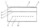
- the substrate-holding device in the form of a ceramic element 1 for probes for testing circuit arrangements on substrates under test 2is described in three different embodiments.
- Waferssuch as semiconductor wafers which are structured as chips, are generally disc-shaped substrates 2 under test.
- the chipsinclude the circuit arrangement to be tested and are present in the complete wafer formation.
- the substrate-holding devices 1 representedhave a surface 3 for the accommodation of a substrate 2 to be tested. In addition, they have provisions, not represented in detail, for holding the substrate 2 to the surface 3 .
- clamping deviceswhich clamp the substrate 2 mechanically onto the surface 3 . This may be necessary when the substrate-holding device 1 is to be used under a vacuum, where vacuum-holding devices would otherwise be unsuitable.
- the substrate-holding device 1is designed as a one-piece ceramic element having variably heavily doped layer regions 4 , 5 , 6 and/or 7 , specifically with an electrically conductive first layer region 4 , an electric insulating second layer region 5 , an electrically conductive third layer region 6 and an electric insulating fourth layer region 7 .
- the first layer region 4has a connection, not represented in detail, for applying a force potential.
- the third layer region 6is provided with a connection, likewise not represented in detail, for applying a guard potential.
- the first layer region 4encloses the entire surface 3 of the ceramic element.
- the second layer region 5 , third layer region 6 and the fourth layer region 7are arranged parallel thereto.
- the fourth layer region 7serves as a bottom outer protective layer, by which the substrate-holding device 1 is placeable on a chuck 9 .
- the chuck 9is acted on by shield potential. This makes it possible to enlarge a conventional chuck 9 functionally for a triaxial structure.
- the chuck 9in principle, it is possible to design the chuck 9 as a thermochuck in order to bring the substrate 2 to a given temperature in which measuring operations are to take place. In this regard, heating as well as cooling is possible.
- heating elements 8are provided in the fourth layer 7 .
- the heating elements 8likewise consists of doped layer regions within the ceramic element, so that its homogeneity need not be disturbed by the arrangement of heating elements 8 .
- the layer regions in the top view, not shown in detail,are designed spiral-like or meandering and have external contact connections to receive a supply of electric energy.
- thermochuck 9With the arrangement of heating element 8 in the fourth layer region 7 , it also becomes possible to combine this substrate-holding device 1 with a thermochuck 9 , the thermochuck 9 then assuming the cooling operations if the substrate 2 must be kept in lower temperature ranges during measurement. Measurement at higher temperatures is obtained by the integrated heating element 8 . The multiplicity of uses of such a combination is thus considerably increased.
- Such heating 8is also provided in the arrangements of FIG. 2 and FIG. 3.
- the first layer region 4while leaving a peripheral region on the surface 3 free, is introduced in the center of surface 3 .
- the second layer region 5projects into the peripheral region of the surface 3 .
- the third layer region 6is designed in a bowl-shaped arrangement which surrounds the first layer 4 and includes sidewall portions that project all the way to the surface 3 in the peripheral region.
- an electrically conductive fifth layer region 10which is acted on by shield potential, is provided in the examples of FIG. 2 and FIG. 3.
- the fifth layer region 10is arranged on the whole outer side of the substrate-holding device 1 , the surface 3 being left exposed.
- the fifth layer region 10is arranged parallel to the first layer 4 all the way to the fourth layer 7 .
- a substrate-holding device 1 for HF measurementis represented in FIG. 4.
- Thishas a first insulating layer 11 , which has an insulating resistance greater than 10 10 to 10 12 ⁇ .
- the first insulating layer region 11like the first layer region 4 in the other representations, encloses at least partially the surface 3 .
- Under the first insulating layer 11there is arranged an absorption layer 12 with high electrical conductivity, less than 10 ⁇ to 10 ⁇ 3 ⁇ cm.
- a second insulating layer 13located under absorption layer 12 , again has a high insulating resistance, greater than 10 10 to 10 12 ⁇ .
- the structure of FIG. 4shows a sequence of layers reversed in conductivity or in insulating resistance.
Landscapes
- Physics & Mathematics (AREA)
- General Physics & Mathematics (AREA)
- Testing Or Measuring Of Semiconductors Or The Like (AREA)
Abstract
Description
- The invention relates to a substrate-holding device for probes for testing circuit arrangements on substrates and more particularly to a monolithic substrate-holding device.[0001]
- A substrate holder of the type mentioned at the beginning is described in U.S. Pat. No. 5,457,398. It has first and second elements that are electrically insulated from one another, the first element of the substrate holder having an upper surface for the horizontal accommodation of a test circuit for testing by an electric probe. The substrate holder is surrounded by a sheath. This arrangement is provided for a triaxial structure. For this purpose, the second element has upper and lower parts, each of which consists of conductive material. In addition, there is applied a first non-zero potential difference between the first element of the clamping device and the outer sheath and a second non-zero potential difference, which is substantially equal to the first potential difference, between the second element of the clamping device and the outer sheath. Hence, the first element carries a force potential, the second element carries a guard potential and the sheath carries a shield potential.[0002]
- The growing number of applications in the field of measurement of low currents in the femtoampere range (10[0003]−15A) and in the attoampere range (10−18A) makes the development of increasingly sensitive measuring equipment necessary. The increasing number of sources of interference (e.g., increasingly stronger wireless message transmission) makes increasingly better shielding or other measuring and compensating methods also necessary. Added to this are additional parameters (e.g., temperature of the substrate) that must be kept spatially and temporally constant with great accuracy during the measuring process. Well thought-out arrangements with careful selection of material are required to obtain spatial constancy of the corresponding specified parameters. Precise and reliable control technology provides appropriate temporal parameter constancy.
- The measurement of small currents with rapid signal rise times requires a measuring arrangement with small parasitic capacities in the signal path and high insulating resistances over the entire temperature range. The observance of parameter temperature necessitates good thermal contact of the substrate. Along with all the rest of the measuring arrangement (e.g. measuring chamber, probe heads and probe needles), the substrate-holding arrangement, or chuck, is of great importance.[0004]
- U.S. Pat. No. 5,610,529 discloses a structure of a substrate holder that has an electrically conductive holding plate. This holding plate adjoins an insulating plate. Below the insulating plate, there is provided a so-called thermochuck, which provides for the addition or removal of energy to or from the substrate, depending on whether it is to be tested at high or low temperatures.[0005]
- Here, addition or removal of thermal energy may be effected conventionally or alternatively by gases or liquids controlled externally and conveyed through the thermochuck, as described in U.S. Pat. Nos. 4,426,619 and 4,734,872.[0006]
- In this arrangement, the holding plate carries a force potential and the thermochuck a guard potential.[0007]
- It has been found that such an arrangement produces non-homogeneities in the conduction of heat to the substrate. As a result, a frictional electric effect, which results in interference with the measurement, cannot be avoided here.[0008]
- Therefore, an object of the invention is to improve the homogeneity of thermal conduction to the substrate and increase the accuracy of measurement.[0009]
- According to the invention, this object is accomplished in that the substrate-holding device is designed as a one-piece ceramic element having variably heavily doped layers. Owing to the one-piece nature of the ceramic element, opposing surfaces defining the interface between layers in the multipart structure according to the prior art, are avoided. This causes a reduction in the influence of the tribolectric effect. In addition, material properties may be adjusted so that they satisfy the technical requirements of conductivity, resistivity and the like. For example, the impedance level of the arrangement is therefore adjustable.[0010]
- In a favorable embodiment of the invention, a ceramic element is doped to provide a first layer region at least partially enclosing the surface that has a high electrical conductivity less than 10[0011]−1to 10−3Ωcm. The ceramic element also includes a second layer region located under the first layer region which exhibits an insulating resistance greater than 1010to 1012Ω and a third layer region located thereunder which is doped to provide a high electrical conductivity less than 10−1to 10−3Ωcm. The first layer is provided with an external contact connection for connection of a force potential and the third layer with an external contact connection for connection to a guard potential.
- The possibility of a triaxial structure is thereby provided. Here, the substrate to be tested is placeable on the first layer, which has a conductive layer. This first layer serves for a carrying force potential.[0012]
- In an alternative embodiment of the invention, it is provided that a first insulating layer at least partially enclosing the surface has an insulating resistance greater than 10[0013]10to 1012Ω, an absorption layer located under the first insulating layer that has a high electrical conductivity less than 10−1to 10−3Ωcm and a second insulating layer located thereunder again that has an insulating resistance greater than 1010to 1012Ω.
- This embodiment makes it possible to perform HF measurements on substrates. There, the first insulating layer with the absorption layer results in an impedance level that is adjustable according to the insulating or dielectric properties of the first insulating layer and the conductivity of the absorption layer.[0014]
- In an additional embodiment of the invention, it is provided that the substrate has under the third layer a fourth layer with a great insulating resistance.[0015]
- This fourth layer serves for insulation of the third layer downward. This may be advantageous in order to arrange additional layers under the third layer or in order to place the arrangement on a conductive element.[0016]
- In one embodiment of the invention, the substrate-holding device is placeable on a thermochuck. Such a thermochuck normally is itself designed for holding substrates. In addition, it has thermo-electric elements for moderating the temperature of the substrate. In this alternate embodiment, the substrate is not placed directly on the thermochuck. Rather, the substrate-holding device according to the invention is arranged between the thermochuck and the substrate. Thus, on the one hand the targeted thermal influence of the substrate may be achieved via the thermochuck. On the other hand, with the use of a standard chuck with the aid of the substrate-holding device according to the invention, a substrate holder according to the triaxial principle may be obtained without the disadvantages of the prior art.[0017]
- Here it is possible to act on the thermochuck with shield potential. Thus, the substrate-holding device, as a relatively thin add-on plate, would be shielded by the thermochuck itself.[0018]
- Another possibility for implementing temperature control of the substrate is that the substrate-holding device is provided in the region of the fourth layer with electric heating elements consisting of doped layer regions. Thus, heating for moderation of the substrate temperature in the interior of the one-piece substrate-holding device is implemented by transit paths as resistance paths in the interior region of the ceramic element thereof.[0019]
- To ensure high surface homogeneity of heating, it is advantageous that the layer regions of heating be designed spiral-like or meandering in the top view and have external contact connections.[0020]
- In an additional embodiment of the invention, it is provided that the first layer is introduced in the center of the surface, leaving free a peripheral region on the surface. The second layer projects in the peripheral region of the surface. The third layer is designed bowl-shaped, surrounds the first layer in the peripheral region and includes side wall portions which project all the way to the surface. It can thus be ensured that the guard potential-carrying third layer surrounds the first layer, so that no interfering effects can occur at the sides of the first layer, either.[0021]
- There are two possibilities for implementation of a shield potential-carrying layer. For one, a fifth layer having high electrical conductivity may be provided under the fourth layer, which is acted on by shield potential.[0022]
- For this purpose, it is advantageous that the fifth layer be arranged on the outside with the surface being left free. Thus, the fifth layer surrounds all the rest of the substrate-holding device and protects it from the outside.[0023]
- The invention will be explained in detail below by way of three specific examples of preferred embodiments. In the accompanying drawing:[0024]
- FIG. 1 is a schematic representation of a cross section through a triaxial substrate-holding device designed as an add-on plate;[0025]
- FIG. 2 is a schematic representation of a cross section through a triaxial substrate-holding device according to the invention with integrated heating;[0026]
- FIG. 3 is a schematic representation of a cross section through a triaxial substrate-holding device according to the invention with a bowl-shaped third layer; and[0027]
- FIG. 4 is a schematic representation of a cross section through a substrate holder according to the invention for HF measurement.[0028]
- In the figures, the substrate-holding device in the form of a[0029]
ceramic element 1 for probes for testing circuit arrangements on substrates undertest 2 is described in three different embodiments. - Wafers, such as semiconductor wafers which are structured as chips, are generally disc-shaped[0030]
substrates 2 under test. The chips include the circuit arrangement to be tested and are present in the complete wafer formation. - The substrate-holding[0031]
devices 1 represented have asurface 3 for the accommodation of asubstrate 2 to be tested. In addition, they have provisions, not represented in detail, for holding thesubstrate 2 to thesurface 3. This generally takes the form of groove-like recesses in thesurface 3, which are connected with a vacuum source. These groove-like recesses are sealed by the placement of thesubstrate 2, owing to which they are able to build up a vacuum in the recesses, which then sucks the underside of thesubstrate 2 onto thesurface 3. - However, other means for holding the[0032]
substrate 2 are alternatively employable, for instance clamping devices, which clamp thesubstrate 2 mechanically onto thesurface 3. This may be necessary when the substrate-holdingdevice 1 is to be used under a vacuum, where vacuum-holding devices would otherwise be unsuitable. - As further shown in the drawing, the substrate-holding[0033]
device 1 is designed as a one-piece ceramic element having variably heavily dopedlayer regions first layer region 4, an electric insulatingsecond layer region 5, an electrically conductivethird layer region 6 and an electric insulatingfourth layer region 7. - The[0034]
first layer region 4 has a connection, not represented in detail, for applying a force potential. Thethird layer region 6 is provided with a connection, likewise not represented in detail, for applying a guard potential. - As shown in FIG. 1, the[0035]
first layer region 4 encloses theentire surface 3 of the ceramic element. Thesecond layer region 5,third layer region 6 and thefourth layer region 7 are arranged parallel thereto. Thefourth layer region 7 serves as a bottom outer protective layer, by which the substrate-holdingdevice 1 is placeable on achuck 9. - The[0036]
chuck 9 is acted on by shield potential. This makes it possible to enlarge aconventional chuck 9 functionally for a triaxial structure. - In principle, it is possible to design the[0037]
chuck 9 as a thermochuck in order to bring thesubstrate 2 to a given temperature in which measuring operations are to take place. In this regard, heating as well as cooling is possible. - As shown in FIG. 1,[0038]
heating elements 8 are provided in thefourth layer 7. Theheating elements 8 likewise consists of doped layer regions within the ceramic element, so that its homogeneity need not be disturbed by the arrangement ofheating elements 8. The layer regions in the top view, not shown in detail, are designed spiral-like or meandering and have external contact connections to receive a supply of electric energy. - With the arrangement of[0039]
heating element 8 in thefourth layer region 7, it also becomes possible to combine this substrate-holdingdevice 1 with athermochuck 9, thethermochuck 9 then assuming the cooling operations if thesubstrate 2 must be kept in lower temperature ranges during measurement. Measurement at higher temperatures is obtained by theintegrated heating element 8. The multiplicity of uses of such a combination is thus considerably increased. - [0040]
Such heating 8 is also provided in the arrangements of FIG. 2 and FIG. 3. - As shown in FIG. 3, the[0041]
first layer region 4, while leaving a peripheral region on thesurface 3 free, is introduced in the center ofsurface 3. Thesecond layer region 5 projects into the peripheral region of thesurface 3. Lastly, thethird layer region 6 is designed in a bowl-shaped arrangement which surrounds thefirst layer 4 and includes sidewall portions that project all the way to thesurface 3 in the peripheral region. - In contrast to the arrangement of FIG. 1, in which the shield function is assumed by the[0042]
chuck 9, an electrically conductivefifth layer region 10, which is acted on by shield potential, is provided in the examples of FIG. 2 and FIG. 3. - According to FIG. 3, the[0043]
fifth layer region 10 is arranged on the whole outer side of the substrate-holdingdevice 1, thesurface 3 being left exposed. - According to FIG. 2, the[0044]
fifth layer region 10 is arranged parallel to thefirst layer 4 all the way to thefourth layer 7. - A substrate-holding[0045]
device 1 for HF measurement is represented in FIG. 4. This has a first insulatinglayer 11, which has an insulating resistance greater than 1010to 1012Ω. The first insulatinglayer region 11, like thefirst layer region 4 in the other representations, encloses at least partially thesurface 3. Under the first insulatinglayer 11, there is arranged anabsorption layer 12 with high electrical conductivity, less than 10−to 10−3Ωcm. Lastly, a second insulatinglayer 13, located underabsorption layer 12, again has a high insulating resistance, greater than 1010to 1012Ω. Thus, the structure of FIG. 4 shows a sequence of layers reversed in conductivity or in insulating resistance.
Claims (10)
Applications Claiming Priority (2)
| Application Number | Priority Date | Filing Date | Title |
|---|---|---|---|
| DE10122036.7 | 2001-05-07 | ||
| DE10122036ADE10122036B4 (en) | 2001-05-07 | 2001-05-07 | Substrate holding device for probes for testing circuit arrangements on disc-shaped substrates |
Publications (2)
| Publication Number | Publication Date |
|---|---|
| US20020163350A1true US20020163350A1 (en) | 2002-11-07 |
| US6864676B2 US6864676B2 (en) | 2005-03-08 |
Family
ID=7683845
Family Applications (1)
| Application Number | Title | Priority Date | Filing Date |
|---|---|---|---|
| US10/139,735Expired - LifetimeUS6864676B2 (en) | 2001-05-07 | 2002-05-06 | Substrate-holding device for testing circuit arrangements on substrates |
Country Status (2)
| Country | Link |
|---|---|
| US (1) | US6864676B2 (en) |
| DE (1) | DE10122036B4 (en) |
Cited By (2)
| Publication number | Priority date | Publication date | Assignee | Title |
|---|---|---|---|---|
| WO2011156049A1 (en)* | 2010-06-07 | 2011-12-15 | Cascade Microtech, Inc. | High voltage chuck for a probe station |
| US20160047856A1 (en)* | 2013-03-27 | 2016-02-18 | (Tokyo Electron Limited) | Probe device |
Families Citing this family (1)
| Publication number | Priority date | Publication date | Assignee | Title |
|---|---|---|---|---|
| DE102005014513B4 (en)* | 2005-03-30 | 2011-05-12 | Att Advanced Temperature Test Systems Gmbh | Device and method for tempering a substrate, and method for producing the device |
Citations (13)
| Publication number | Priority date | Publication date | Assignee | Title |
|---|---|---|---|---|
| US5151845A (en)* | 1988-09-19 | 1992-09-29 | Toto Ltd. | Electrostatic chuck |
| US5191506A (en)* | 1991-05-02 | 1993-03-02 | International Business Machines Corporation | Ceramic electrostatic chuck |
| US5207437A (en)* | 1991-10-29 | 1993-05-04 | International Business Machines Corporation | Ceramic electrostatic wafer chuck |
| US5208156A (en)* | 1990-03-13 | 1993-05-04 | Tanabe Seiyaku Co., Ltd. | Esterase purified from serratia marcescens sr41 (ferm bp-no. 487) |
| US5280156A (en)* | 1990-12-25 | 1994-01-18 | Ngk Insulators, Ltd. | Wafer heating apparatus and with ceramic substrate and dielectric layer having electrostatic chucking means |
| US5457398A (en)* | 1992-06-11 | 1995-10-10 | Cascade Microtech, Inc. | Wafer probe station having full guarding |
| US5539179A (en)* | 1990-11-17 | 1996-07-23 | Tokyo Electron Limited | Electrostatic chuck having a multilayer structure for attracting an object |
| US5610529A (en)* | 1995-04-28 | 1997-03-11 | Cascade Microtech, Inc. | Probe station having conductive coating added to thermal chuck insulator |
| US5646814A (en)* | 1994-07-15 | 1997-07-08 | Applied Materials, Inc. | Multi-electrode electrostatic chuck |
| US5909355A (en)* | 1997-12-02 | 1999-06-01 | Applied Materials, Inc. | Ceramic electrostatic chuck and method of fabricating same |
| US6133557A (en)* | 1995-01-31 | 2000-10-17 | Kyocera Corporation | Wafer holding member |
| US6188563B1 (en)* | 1997-09-18 | 2001-02-13 | Trikon Equipments Limited | Platen for semiconductor workpieces |
| US6259592B1 (en)* | 1998-11-19 | 2001-07-10 | Applied Materials, Inc. | Apparatus for retaining a workpiece upon a workpiece support and method of manufacturing same |
Family Cites Families (4)
| Publication number | Priority date | Publication date | Assignee | Title |
|---|---|---|---|---|
| US4426619A (en)* | 1981-06-03 | 1984-01-17 | Temptronic Corporation | Electrical testing system including plastic window test chamber and method of using same |
| US4734872A (en)* | 1985-04-30 | 1988-03-29 | Temptronic Corporation | Temperature control for device under test |
| TW303505B (en)* | 1996-05-08 | 1997-04-21 | Applied Materials Inc | Substrate support chuck having a contaminant containment layer and method of fabricating same |
| US6529362B2 (en)* | 1997-03-06 | 2003-03-04 | Applied Materials Inc. | Monocrystalline ceramic electrostatic chuck |
- 2001
- 2001-05-07DEDE10122036Apatent/DE10122036B4/ennot_activeExpired - Fee Related
- 2002
- 2002-05-06USUS10/139,735patent/US6864676B2/ennot_activeExpired - Lifetime
Patent Citations (13)
| Publication number | Priority date | Publication date | Assignee | Title |
|---|---|---|---|---|
| US5151845A (en)* | 1988-09-19 | 1992-09-29 | Toto Ltd. | Electrostatic chuck |
| US5208156A (en)* | 1990-03-13 | 1993-05-04 | Tanabe Seiyaku Co., Ltd. | Esterase purified from serratia marcescens sr41 (ferm bp-no. 487) |
| US5539179A (en)* | 1990-11-17 | 1996-07-23 | Tokyo Electron Limited | Electrostatic chuck having a multilayer structure for attracting an object |
| US5280156A (en)* | 1990-12-25 | 1994-01-18 | Ngk Insulators, Ltd. | Wafer heating apparatus and with ceramic substrate and dielectric layer having electrostatic chucking means |
| US5191506A (en)* | 1991-05-02 | 1993-03-02 | International Business Machines Corporation | Ceramic electrostatic chuck |
| US5207437A (en)* | 1991-10-29 | 1993-05-04 | International Business Machines Corporation | Ceramic electrostatic wafer chuck |
| US5457398A (en)* | 1992-06-11 | 1995-10-10 | Cascade Microtech, Inc. | Wafer probe station having full guarding |
| US5646814A (en)* | 1994-07-15 | 1997-07-08 | Applied Materials, Inc. | Multi-electrode electrostatic chuck |
| US6133557A (en)* | 1995-01-31 | 2000-10-17 | Kyocera Corporation | Wafer holding member |
| US5610529A (en)* | 1995-04-28 | 1997-03-11 | Cascade Microtech, Inc. | Probe station having conductive coating added to thermal chuck insulator |
| US6188563B1 (en)* | 1997-09-18 | 2001-02-13 | Trikon Equipments Limited | Platen for semiconductor workpieces |
| US5909355A (en)* | 1997-12-02 | 1999-06-01 | Applied Materials, Inc. | Ceramic electrostatic chuck and method of fabricating same |
| US6259592B1 (en)* | 1998-11-19 | 2001-07-10 | Applied Materials, Inc. | Apparatus for retaining a workpiece upon a workpiece support and method of manufacturing same |
Cited By (8)
| Publication number | Priority date | Publication date | Assignee | Title |
|---|---|---|---|---|
| WO2011156049A1 (en)* | 2010-06-07 | 2011-12-15 | Cascade Microtech, Inc. | High voltage chuck for a probe station |
| WO2011159390A1 (en)* | 2010-06-07 | 2011-12-22 | Cascade Microtech, Inc. | High voltage chuck for a probe station |
| EP2577334A4 (en)* | 2010-06-07 | 2014-01-01 | Cascade Microtech Inc | HIGH VOLTAGE SUPPORT FOR TEST STATION |
| US9506973B2 (en) | 2010-06-07 | 2016-11-29 | Cascade Microtech, Inc. | High voltage chuck for a probe station |
| US9741599B2 (en) | 2010-06-07 | 2017-08-22 | Cascade Microtech, Inc. | High voltage chuck for a probe station |
| US10062597B2 (en) | 2010-06-07 | 2018-08-28 | Formfactor Beaverton, Inc. | High voltage chuck for a probe station |
| US20160047856A1 (en)* | 2013-03-27 | 2016-02-18 | (Tokyo Electron Limited) | Probe device |
| US9739828B2 (en)* | 2013-03-27 | 2017-08-22 | Tokyo Electron Limited | Probe device |
Also Published As
| Publication number | Publication date |
|---|---|
| DE10122036A1 (en) | 2002-12-12 |
| DE10122036B4 (en) | 2009-12-24 |
| US6864676B2 (en) | 2005-03-08 |
Similar Documents
| Publication | Publication Date | Title |
|---|---|---|
| US6424141B1 (en) | Wafer probe station | |
| US7138813B2 (en) | Probe station thermal chuck with shielding for capacitive current | |
| US10978323B2 (en) | Substrate holder having integrated temperature measurement electrical devices | |
| KR100257667B1 (en) | Probe station having conductive coating added to themal chuck insulator | |
| US9029728B2 (en) | Methods of and apparatuses for measuring electrical parameters of a plasma process | |
| US6406545B2 (en) | Semiconductor workpiece processing apparatus and method | |
| JP3227026B2 (en) | Probe station | |
| US4884026A (en) | Electrical characteristic measuring apparatus | |
| JPH1093346A (en) | Oven assembly for oscillator | |
| KR102273513B1 (en) | Mounting table, and method of manufacturing the mounting table | |
| US6864676B2 (en) | Substrate-holding device for testing circuit arrangements on substrates | |
| JPS58220438A (en) | Measuring placing stand for semiconductor wafer | |
| JPS63138745A (en) | Structure of base plate for prober | |
| JP2004063486A (en) | Chuck mechanism for prober | |
| JPH0762691B2 (en) | Electrical property measuring device | |
| KR20210114481A (en) | Heater temperature control method, heater and mount | |
| JPH08330369A (en) | Interface card for prober | |
| JPH08111438A (en) | Probe for integrated circuit element | |
| JPH01303733A (en) | Probe device | |
| JP2664929B2 (en) | Resistance measuring instrument | |
| JP2618926B2 (en) | Electrical property measurement system | |
| JPH02166746A (en) | Measuring apparatus | |
| JPS639945A (en) | Measuring method of electrical characteristic in vacuum |
Legal Events
| Date | Code | Title | Description |
|---|---|---|---|
| AS | Assignment | Owner name:SUSS MICROTEC TESTSYSTEMS (GMBH), GERMANY Free format text:ASSIGNMENT OF ASSIGNORS INTEREST;ASSIGNORS:KIESEWETTER, JORG;TEICH, MICHAEL;SCHNEIDEWIND, STEFAN;AND OTHERS;REEL/FRAME:012877/0053 Effective date:20020505 | |
| STCF | Information on status: patent grant | Free format text:PATENTED CASE | |
| FPAY | Fee payment | Year of fee payment:4 | |
| AS | Assignment | Owner name:CASCADE MICROTECH, INC., OREGON Free format text:MERGER;ASSIGNOR:SUSS MICROTEC TEST SYSTEMS GMBH;REEL/FRAME:026246/0706 Effective date:20100127 | |
| FEPP | Fee payment procedure | Free format text:PAT HOLDER CLAIMS SMALL ENTITY STATUS, ENTITY STATUS SET TO SMALL (ORIGINAL EVENT CODE: LTOS); ENTITY STATUS OF PATENT OWNER: LARGE ENTITY | |
| REMI | Maintenance fee reminder mailed | ||
| FPAY | Fee payment | Year of fee payment:8 | |
| SULP | Surcharge for late payment | Year of fee payment:7 | |
| FEPP | Fee payment procedure | Free format text:PAT HOLDER NO LONGER CLAIMS SMALL ENTITY STATUS, ENTITY STATUS SET TO UNDISCOUNTED (ORIGINAL EVENT CODE: STOL); ENTITY STATUS OF PATENT OWNER: LARGE ENTITY | |
| AS | Assignment | Owner name:HSBC BANK USA, NATIONAL ASSOCIATION, CALIFORNIA Free format text:SECURITY INTEREST IN UNITED STATES PATENTS AND TRADEMARKS;ASSIGNORS:FORMFACTOR, INC.;ASTRIA SEMICONDUCTOR HOLDINGS, INC.;CASCADE MICROTECH, INC.;AND OTHERS;REEL/FRAME:039184/0280 Effective date:20160624 | |
| FPAY | Fee payment | Year of fee payment:12 | |
| AS | Assignment | Owner name:FORMFACTOR BEAVERTON, INC., OREGON Free format text:CHANGE OF NAME;ASSIGNOR:CASCADE MICROTECH, INC.;REEL/FRAME:046573/0664 Effective date:20180514 | |
| AS | Assignment | Owner name:FORMFACTOR, INC., CALIFORNIA Free format text:ASSIGNMENT OF ASSIGNORS INTEREST;ASSIGNOR:FORMFACTOR BEAVERTON, INC.;REEL/FRAME:057393/0609 Effective date:20210826 | |
| AS | Assignment | Owner name:WELLS FARGO BANK, NATIONAL ASSOCIATION, AS ADMINISTRATIVE AGENT, TEXAS Free format text:SECURITY INTEREST;ASSIGNOR:FORMFACTOR, INC.;REEL/FRAME:072263/0272 Effective date:20250729 |