US20020160551A1 - Memory elements and methods for making same - Google Patents
Memory elements and methods for making sameDownload PDFInfo
- Publication number
- US20020160551A1 US20020160551A1US09/809,561US80956101AUS2002160551A1US 20020160551 A1US20020160551 A1US 20020160551A1US 80956101 AUS80956101 AUS 80956101AUS 2002160551 A1US2002160551 A1US 2002160551A1
- Authority
- US
- United States
- Prior art keywords
- layer
- contact
- memory
- substrate
- chalcogenide
- Prior art date
- Legal status (The legal status is an assumption and is not a legal conclusion. Google has not performed a legal analysis and makes no representation as to the accuracy of the status listed.)
- Granted
Links
- 230000015654memoryEffects0.000titleclaimsabstractdescription215
- 238000000034methodMethods0.000titleclaimsabstractdescription70
- 239000000463materialSubstances0.000claimsabstractdescription136
- 239000004020conductorSubstances0.000claimsabstractdescription32
- 230000008569processEffects0.000claimsabstractdescription26
- 238000005530etchingMethods0.000claimsabstractdescription11
- 150000004770chalcogenidesChemical class0.000claimsdescription123
- 239000000758substrateSubstances0.000claimsdescription51
- 239000004065semiconductorSubstances0.000claimsdescription23
- 239000011810insulating materialSubstances0.000claimsdescription6
- 230000008021depositionEffects0.000abstractdescription11
- OKTJSMMVPCPJKN-UHFFFAOYSA-NCarbonChemical compound[C]OKTJSMMVPCPJKN-UHFFFAOYSA-N0.000abstractdescription9
- 229910052799carbonInorganic materials0.000abstractdescription9
- NRTOMJZYCJJWKI-UHFFFAOYSA-NTitanium nitrideChemical compound[Ti]#NNRTOMJZYCJJWKI-UHFFFAOYSA-N0.000abstractdescription6
- 239000000126substanceSubstances0.000abstractdescription2
- 239000011148porous materialSubstances0.000description27
- 239000010408filmSubstances0.000description26
- 125000006850spacer groupChemical group0.000description21
- 230000015572biosynthetic processEffects0.000description20
- 238000000151depositionMethods0.000description11
- 238000004519manufacturing processMethods0.000description11
- 239000011159matrix materialSubstances0.000description10
- 230000008901benefitEffects0.000description8
- VYPSYNLAJGMNEJ-UHFFFAOYSA-NSilicium dioxideChemical compoundO=[Si]=OVYPSYNLAJGMNEJ-UHFFFAOYSA-N0.000description6
- 239000007772electrode materialSubstances0.000description6
- 229910052581Si3N4Inorganic materials0.000description5
- 239000003989dielectric materialSubstances0.000description5
- HQVNEWCFYHHQES-UHFFFAOYSA-Nsilicon nitrideChemical compoundN12[Si]34N5[Si]62N3[Si]51N64HQVNEWCFYHHQES-UHFFFAOYSA-N0.000description5
- 229910045601alloyInorganic materials0.000description4
- 239000000956alloySubstances0.000description4
- 230000008859changeEffects0.000description4
- 230000006870functionEffects0.000description4
- 229910052732germaniumInorganic materials0.000description4
- 230000003287optical effectEffects0.000description4
- 238000005240physical vapour depositionMethods0.000description4
- 238000003860storageMethods0.000description4
- 229910052714telluriumInorganic materials0.000description4
- 229910052787antimonyInorganic materials0.000description3
- 230000015556catabolic processEffects0.000description3
- GNPVGFCGXDBREM-UHFFFAOYSA-Ngermanium atomChemical compound[Ge]GNPVGFCGXDBREM-UHFFFAOYSA-N0.000description3
- 230000004044responseEffects0.000description3
- 235000012239silicon dioxideNutrition0.000description3
- 239000000377silicon dioxideSubstances0.000description3
- 238000001228spectrumMethods0.000description3
- PORWMNRCUJJQNO-UHFFFAOYSA-Ntellurium atomChemical compound[Te]PORWMNRCUJJQNO-UHFFFAOYSA-N0.000description3
- XKRFYHLGVUSROY-UHFFFAOYSA-NArgonChemical compound[Ar]XKRFYHLGVUSROY-UHFFFAOYSA-N0.000description2
- WATWJIUSRGPENY-UHFFFAOYSA-Nantimony atomChemical compound[Sb]WATWJIUSRGPENY-UHFFFAOYSA-N0.000description2
- 238000011161developmentMethods0.000description2
- 230000018109developmental processEffects0.000description2
- BHEPBYXIRTUNPN-UHFFFAOYSA-Nhydridophosphorus(.) (triplet)Chemical compound[PH]BHEPBYXIRTUNPN-UHFFFAOYSA-N0.000description2
- 230000005012migrationEffects0.000description2
- 238000013508migrationMethods0.000description2
- 238000012986modificationMethods0.000description2
- 230000004048modificationEffects0.000description2
- 229910052760oxygenInorganic materials0.000description2
- 239000001301oxygenSubstances0.000description2
- 239000012782phase change materialSubstances0.000description2
- 229910021420polycrystalline siliconInorganic materials0.000description2
- 229920005591polysiliconPolymers0.000description2
- 229910052711seleniumInorganic materials0.000description2
- 239000011669seleniumSubstances0.000description2
- 239000010409thin filmSubstances0.000description2
- 238000012546transferMethods0.000description2
- WQJQOUPTWCFRMM-UHFFFAOYSA-Ntungsten disilicideChemical compound[Si]#[W]#[Si]WQJQOUPTWCFRMM-UHFFFAOYSA-N0.000description2
- 229910021342tungsten silicideInorganic materials0.000description2
- ZOXJGFHDIHLPTG-UHFFFAOYSA-NBoronChemical compound[B]ZOXJGFHDIHLPTG-UHFFFAOYSA-N0.000description1
- RYGMFSIKBFXOCR-UHFFFAOYSA-NCopperChemical compound[Cu]RYGMFSIKBFXOCR-UHFFFAOYSA-N0.000description1
- XPDWGBQVDMORPB-UHFFFAOYSA-NFluoroformChemical compoundFC(F)FXPDWGBQVDMORPB-UHFFFAOYSA-N0.000description1
- BUGBHKTXTAQXES-UHFFFAOYSA-NSeleniumChemical compound[Se]BUGBHKTXTAQXES-UHFFFAOYSA-N0.000description1
- XUIMIQQOPSSXEZ-UHFFFAOYSA-NSiliconChemical compound[Si]XUIMIQQOPSSXEZ-UHFFFAOYSA-N0.000description1
- NINIDFKCEFEMDL-UHFFFAOYSA-NSulfurChemical compound[S]NINIDFKCEFEMDL-UHFFFAOYSA-N0.000description1
- RTAQQCXQSZGOHL-UHFFFAOYSA-NTitaniumChemical compound[Ti]RTAQQCXQSZGOHL-UHFFFAOYSA-N0.000description1
- 238000010521absorption reactionMethods0.000description1
- 230000002411adverseEffects0.000description1
- 229910052782aluminiumInorganic materials0.000description1
- XAGFODPZIPBFFR-UHFFFAOYSA-NaluminiumChemical compound[Al]XAGFODPZIPBFFR-UHFFFAOYSA-N0.000description1
- 229910052786argonInorganic materials0.000description1
- 229910052785arsenicInorganic materials0.000description1
- RQNWIZPPADIBDY-UHFFFAOYSA-Narsenic atomChemical compound[As]RQNWIZPPADIBDY-UHFFFAOYSA-N0.000description1
- QVGXLLKOCUKJST-UHFFFAOYSA-Natomic oxygenChemical compound[O]QVGXLLKOCUKJST-UHFFFAOYSA-N0.000description1
- 230000004888barrier functionEffects0.000description1
- 229910052797bismuthInorganic materials0.000description1
- JCXGWMGPZLAOME-UHFFFAOYSA-Nbismuth atomChemical compound[Bi]JCXGWMGPZLAOME-UHFFFAOYSA-N0.000description1
- 229910052796boronInorganic materials0.000description1
- 238000005229chemical vapour depositionMethods0.000description1
- 229910052802copperInorganic materials0.000description1
- 239000010949copperSubstances0.000description1
- 230000007423decreaseEffects0.000description1
- 230000001419dependent effectEffects0.000description1
- 238000013461designMethods0.000description1
- 238000005516engineering processMethods0.000description1
- 239000011521glassSubstances0.000description1
- -1i.e.Substances0.000description1
- 239000000203mixtureSubstances0.000description1
- 229910052759nickelInorganic materials0.000description1
- 239000012811non-conductive materialSubstances0.000description1
- 238000001579optical reflectometryMethods0.000description1
- 238000004806packaging method and processMethods0.000description1
- 239000002245particleSubstances0.000description1
- 238000000059patterningMethods0.000description1
- 230000000737periodic effectEffects0.000description1
- 230000002093peripheral effectEffects0.000description1
- 238000000206photolithographyMethods0.000description1
- 238000012545processingMethods0.000description1
- 230000008672reprogrammingEffects0.000description1
- 229910052710siliconInorganic materials0.000description1
- 239000010703siliconSubstances0.000description1
- 229910052712strontiumInorganic materials0.000description1
- CIOAGBVUUVVLOB-UHFFFAOYSA-Nstrontium atomChemical compound[Sr]CIOAGBVUUVVLOB-UHFFFAOYSA-N0.000description1
- 229910052717sulfurInorganic materials0.000description1
- 239000011593sulfurSubstances0.000description1
- 238000012360testing methodMethods0.000description1
- 229910052719titaniumInorganic materials0.000description1
- 239000010936titaniumSubstances0.000description1
- WFKWXMTUELFFGS-UHFFFAOYSA-NtungstenChemical compound[W]WFKWXMTUELFFGS-UHFFFAOYSA-N0.000description1
- 229910052721tungstenInorganic materials0.000description1
- 239000010937tungstenSubstances0.000description1
Images


Classifications
- H—ELECTRICITY
- H10—SEMICONDUCTOR DEVICES; ELECTRIC SOLID-STATE DEVICES NOT OTHERWISE PROVIDED FOR
- H10B—ELECTRONIC MEMORY DEVICES
- H10B63/00—Resistance change memory devices, e.g. resistive RAM [ReRAM] devices
- H10B63/80—Arrangements comprising multiple bistable or multi-stable switching components of the same type on a plane parallel to the substrate, e.g. cross-point arrays
- H10B63/82—Arrangements comprising multiple bistable or multi-stable switching components of the same type on a plane parallel to the substrate, e.g. cross-point arrays the switching components having a common active material layer
- H—ELECTRICITY
- H10—SEMICONDUCTOR DEVICES; ELECTRIC SOLID-STATE DEVICES NOT OTHERWISE PROVIDED FOR
- H10D—INORGANIC ELECTRIC SEMICONDUCTOR DEVICES
- H10D64/00—Electrodes of devices having potential barriers
- H10D64/60—Electrodes characterised by their materials
- H10D64/62—Electrodes ohmically coupled to a semiconductor
- H—ELECTRICITY
- H10—SEMICONDUCTOR DEVICES; ELECTRIC SOLID-STATE DEVICES NOT OTHERWISE PROVIDED FOR
- H10N—ELECTRIC SOLID-STATE DEVICES NOT OTHERWISE PROVIDED FOR
- H10N70/00—Solid-state devices having no potential barriers, and specially adapted for rectifying, amplifying, oscillating or switching
- H10N70/011—Manufacture or treatment of multistable switching devices
- H10N70/061—Shaping switching materials
- H10N70/068—Shaping switching materials by processes specially adapted for achieving sub-lithographic dimensions, e.g. using spacers
- H—ELECTRICITY
- H10—SEMICONDUCTOR DEVICES; ELECTRIC SOLID-STATE DEVICES NOT OTHERWISE PROVIDED FOR
- H10N—ELECTRIC SOLID-STATE DEVICES NOT OTHERWISE PROVIDED FOR
- H10N70/00—Solid-state devices having no potential barriers, and specially adapted for rectifying, amplifying, oscillating or switching
- H10N70/20—Multistable switching devices, e.g. memristors
- H10N70/231—Multistable switching devices, e.g. memristors based on solid-state phase change, e.g. between amorphous and crystalline phases, Ovshinsky effect
- H—ELECTRICITY
- H10—SEMICONDUCTOR DEVICES; ELECTRIC SOLID-STATE DEVICES NOT OTHERWISE PROVIDED FOR
- H10N—ELECTRIC SOLID-STATE DEVICES NOT OTHERWISE PROVIDED FOR
- H10N70/00—Solid-state devices having no potential barriers, and specially adapted for rectifying, amplifying, oscillating or switching
- H10N70/801—Constructional details of multistable switching devices
- H10N70/821—Device geometry
- H10N70/826—Device geometry adapted for essentially vertical current flow, e.g. sandwich or pillar type devices
- H10N70/8265—Device geometry adapted for essentially vertical current flow, e.g. sandwich or pillar type devices on sidewalls of dielectric structures, e.g. mesa-shaped or cup-shaped devices
- H—ELECTRICITY
- H10—SEMICONDUCTOR DEVICES; ELECTRIC SOLID-STATE DEVICES NOT OTHERWISE PROVIDED FOR
- H10N—ELECTRIC SOLID-STATE DEVICES NOT OTHERWISE PROVIDED FOR
- H10N70/00—Solid-state devices having no potential barriers, and specially adapted for rectifying, amplifying, oscillating or switching
- H10N70/801—Constructional details of multistable switching devices
- H10N70/841—Electrodes
- H10N70/8418—Electrodes adapted for focusing electric field or current, e.g. tip-shaped
- H—ELECTRICITY
- H10—SEMICONDUCTOR DEVICES; ELECTRIC SOLID-STATE DEVICES NOT OTHERWISE PROVIDED FOR
- H10N—ELECTRIC SOLID-STATE DEVICES NOT OTHERWISE PROVIDED FOR
- H10N70/00—Solid-state devices having no potential barriers, and specially adapted for rectifying, amplifying, oscillating or switching
- H10N70/801—Constructional details of multistable switching devices
- H10N70/881—Switching materials
- H10N70/882—Compounds of sulfur, selenium or tellurium, e.g. chalcogenides
- H10N70/8828—Tellurides, e.g. GeSbTe
- Y—GENERAL TAGGING OF NEW TECHNOLOGICAL DEVELOPMENTS; GENERAL TAGGING OF CROSS-SECTIONAL TECHNOLOGIES SPANNING OVER SEVERAL SECTIONS OF THE IPC; TECHNICAL SUBJECTS COVERED BY FORMER USPC CROSS-REFERENCE ART COLLECTIONS [XRACs] AND DIGESTS
- Y10—TECHNICAL SUBJECTS COVERED BY FORMER USPC
- Y10S—TECHNICAL SUBJECTS COVERED BY FORMER USPC CROSS-REFERENCE ART COLLECTIONS [XRACs] AND DIGESTS
- Y10S257/00—Active solid-state devices, e.g. transistors, solid-state diodes
- Y10S257/91—Diode arrays, e.g. diode read-only memory array
Definitions
- the inventionrelates generally to the field of semiconductor devices and fabrication and, more particularly, to memory elements and methods for making memory elements.
- Microprocessor-controlled integrated circuitsare used in a wide variety of applications. Such applications include personal computers, vehicle control systems, telephone networks, and a host of consumer products. As is well known, microprocessors are essentially generic devices that perform specific functions under the control of a software program. This program is stored in a memory device coupled to the microprocessor. Not only does the microprocessor access a memory device to retrieve the program instructions, it also stores and retrieves data created during execution of the program in one or more memory devices.
- NVRAMnonvolatile random access memory
- phase change materialscan be electrically switched between a first structural state, in which the material is generally amorphous, and a second structural state, in which the material has a generally crystalline local order.
- the materialmay also be electrically switched between different detectable states of local order across the entire spectrum between the completely amorphous and the completely crystalline states.
- the switching of such materialsis not required to take place in a binary fashion between completely amorphous and completely crystalline states.
- the materialmay be switched in incremental steps reflecting changes of local order to provide a “gray scale” represented by a multiplicity of conditions of local order spanning the spectrum from the completely amorphous state to the completely crystalline state.
- These memory elementsare monolithic, homogeneous, and formed of chalcogenide material typically selected from the group of Te, Se, Sb, Ni, and Ge.
- This chalcogenide materialexhibits different electrical characteristics depending upon its state. For instance, in its amorphous state the material exhibits a higher resistivity than it does in its crystalline state.
- Such chalcogenide materialsmay be switched between numerous electrically detectable conditions of varying resistivity in nanosecond time periods with the input of picojoules of energy.
- the resulting memory elementis truly non-volatile. It will maintain the integrity of the information stored by the memory cell without the need for periodic refresh signals, and the data integrity of the information stored by these memory cells is not lost when power is removed from the device.
- the memory materialis also directly overwritable so that the memory cells need not be erased, i.e., set to a specified starting point, in order to change information stored within the memory cells.
- the large dynamic range offered by the memory materialtheoretically provides for the gray scale storage of multiple bits of binary information in a single cell by mimicking the binary encoded information in analog form and, thereby, storing multiple bits of binary encoded information as a single resistance value in a single cell.
- chalcogenide memory cellsrequire that a region of the chalcogenide memory material, called the “active region,” be subjected to a current pulse to change the crystalline state of the chalcogenide material within the active region.
- a current densitytypically of between about 10 5 and 10 7 amperes/cm 2 is needed.
- the active region of each memory cellshould be made as small as possible to minimize the total current drawn by the memory device.
- chalcogenide memory cellsare fabricated by first creating a diode in a semiconductor substrate. A lower electrode is created over the diode, and a layer of dielectric material is deposited onto the lower electrode. A small opening is created in the dielectric layer. A second dielectric layer, typically of silicon nitride, is then deposited onto the dielectric layer and into the opening. The second dielectric layer is typically about 40 Angstroms thick. The chalcogenide material is then deposited over the second dielectric material and into the opening. An upper electrode material is then deposited over the chalcogenide material.
- a conductive pathis then provided from the chalcogenide material to the lower electrode material by forming a pore in the second dielectric layer by a process known as “popping.” Popping involves passing an initial high current pulse through the structure to cause the second dielectric layer to breakdown. This dielectric breakdown produces a conductive path through the memory cell. Unfortunately, electrically popping the thin silicon nitride layer is not desirable for a high density memory product due to the high current and the large amount of testing time required. Furthermore, this technique may produce memory cells with differing operational characteristics, because the amount of dielectric breakdown may vary from cell to cell.
- the active regions of the chalcogenide memory material within the pores of the dielectric material created by the popping techniqueare believed to change crystalline structure in response to applied voltage pulses of a wide range of magnitudes and pulse durations. These changes in crystalline structure alter the bulk resistance of the chalcogenide active region. Factors such as pore dimensions (e.g., diameter, thickness, and volume), chalcogenide composition, signal pulse duration, and signal pulse waveform shape may affect the magnitude of the dynamic range of resistances, the absolute endpoint resistances of the dynamic range, and the voltages required to set the memory cells at these resistances.
- relatively thick chalcogenide filmse.g., about 4000 Angstroms
- relatively thin chalcogenide layerse.g., about 500 Angstroms
- lower programming voltage requirementse.g., about 1-7 volts.
- one theorysuggests reducing the volume of the active region.
- Another theorysuggests that the cross-sectional area of the pore should be reduced to reduce the size of the chalcogenide element.
- the currenthas little room to spread, and, thus, keeps the active region small.
- the present inventionis directed to overcoming, or at least reducing the affects of, one or more of the problems set forth above.
- a method of forming a contact structure in a semiconductor deviceincludes the acts of: providing a substrate; forming a structure on the substrate, the structure protruding from the substrate and having at least one corner; forming a conformal insulative layer over the structure; and selectively etching away a portion of the conformal insulative material to expose the at least one corner of the structure to form at least one point contact.
- a method of forming a memory structure in a semiconductor deviceincludes the acts of: providing a substrate; forming a structure on the substrate, the structure protruding from the substrate and having at least one corner, and the structure comprising one of a first conductive material and a first memory material; forming a conformal insulative layer over the structure; selectively etching away a portion of the conformal insulative material to expose the at least one corner of the structure to form at least one point contact; forming at least one layer of material over the at least one point contact, the at least one layer of material comprising a second conductive material if the structure comprises the first memory material, and the at least one layer of material comprising a second memory material if the structure comprises the first conductive material; and forming a conductive layer over the at least one layer of material if the at least one layer of material comprises the second memory material.
- a contactin accordance with still another aspect of the present invention, there is provided a contact.
- the contactincludes a substrate.
- a structureprotrudes from the substrate, and the structure has at least one corner.
- a layer of insulating materialis disposed over the structure in a manner that leaves the at least one corner of the structure exposed.
- a memory cellin accordance with yet another aspect of the present invention, there is provided a memory cell.
- the memory cellincludes a substrate.
- a structureprotrudes from the substrate, and the structure has at least one corner.
- the structurecomprises one of a first conductive material and a first memory material.
- a layer of insulating materialis disposed over the structure in a manner that leaves the at least one corner of the structure exposed to form at least one point contact.
- At least one layer of materialis disposed over the at least one point contact.
- the at least one layer of materialcomprises a second conductive material if the structure comprises the first memory material, and the at least one layer of material comprises a second memory material if the structure comprises the first conductive material.
- a conductive layeris disposed over the at least one layer of material if the at least one layer of material comprises the second memory material.
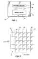
- FIG. 1illustrates a schematic depiction of a substrate containing a memory device which includes a memory matrix and peripheral circuitry;
- FIG. 2illustrates an exemplary schematic depiction of the memory matrix or array of FIG. 1;
- FIG. 3illustrates an exemplary memory cell having a memory element, such as a resistor, and an access device, such as a diode;
- FIG. 4illustrates a top view of a portion of a semiconductor memory array
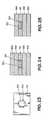
- FIG. 5illustrates a cross-sectional view of an exemplary memory cell at an early stage of fabrication
- FIG. 6, FIG. 7, and FIG. 8illustrate the formation of a spacer and a small pore for the exemplary memory element
- FIG. 9illustrates the small pore of the memory element
- FIG. 10 and FIG. 11illustrate the formation of an electrode in the small pore
- FIG. 12illustrates the deposition of memory material over the lower electrode
- FIG. 13illustrates the deposition of the upper electrode of the memory cell
- FIG. 14illustrates the deposition of an insulative layer and an oxide layer over the upper electrode of the memory cell
- FIG. 15illustrates the formation of a contact extending through the oxide and insulative layer to contact the upper electrode
- FIG. 16illustrates a flow chart depicting an illustrative method of fabricating an annular contact
- FIG. 17illustrates a conductive layer over a substrate
- FIG. 18illustrates a dielectric layer on the structure of FIG. 17
- FIG. 19illustrates a window or trench in the dielectric layer of FIG. 18
- FIG. 20illustrates a conductive or chalcogenide layer on the structure of FIG. 19
- FIG. 21illustrates a dielectric layer on the structure of FIG. 20
- FIG. 22illustrates the formation of a contact by removal of the dielectric layer from the surface of the structure of FIG. 21;
- FIG. 23illustrates a top view of the structure of FIG. 22
- FIG. 24illustrates a chalcogenide layer and a conductive layer on the structure of FIG. 22;
- FIG. 25illustrates an alternative embodiment
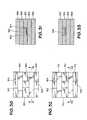
- FIGS. 26 through 33illustrate the formation of linear electrodes using processes similar to those used in reference to FIGS. 16 through 25;
- FIGS. 34 through 38illustrate the formation of electrodes using facet etch processes
- FIGS. 39 through 41illustrate the formation of a first electrode embodiment using facet etch processes
- FIGS. 42 - 46illustrate the formation of a second electrode embodiment using facet etch processes.
- the memory device 10is an integrated circuit memory that is advantageously formed on a semiconductor substrate 12 .
- the memory device 10includes a memory matrix or array 14 that includes a plurality of memory cells for storing data, as described below.
- the memory matrix 14is coupled to periphery circuitry 16 by the plurality of control lines 18 .
- the periphery circuitry 16may include circuitry for addressing the memory cells contained within the memory matrix 14 , along with circuitry for storing data in and retrieving data from the memory cells.
- the periphery circuitry 16may also include other circuitry used for controlling or otherwise insuring the proper functioning of the memory device 10 .
- the memory matrix 14includes a plurality of memory cells 20 that are arranged in generally perpendicular rows and columns.
- the memory cells 20 in each roware coupled together by a respective word line 22
- the memory cells 20 in each columnare coupled together by a respective digit line 24 .
- each memory cell 20includes a word line node 26 that is coupled to a respective word line 22
- each memory cell 20includes a digit line node 28 that is coupled to a respective digit line 24 .
- the conductive word lines 22 and digit lines 24are collectively referred to as address lines. These address lines are electrically coupled to the periphery circuitry 16 so that each of the memory cells 20 can be accessed for the storage and retrieval of information.
- FIG. 3illustrates an exemplary memory cell 20 that may be used in the memory matrix 14 .
- the memory cell 20includes a memory element 30 which is coupled to an access device 32 .
- the memory element 30is illustrated as a programmable resistive element
- the access device 32is illustrated as a diode.
- the programmable resistive elementmay be made of a chalcogenide material, as will be more fully explained below.
- the diode 32may be a conventional diode, a zener diode, or an avalanche diode, depending upon whether the diode array of the memory matrix 14 is operated in a forward biased mode or a reverse biased mode.
- the memory element 30is coupled to a word line 22
- the access device 32is coupled to a digit line 24 .
- connections of the memory element 20may be reversed without adversely affecting the operation of the memory matrix 14 .
- a chalcogenide resistormay be used as the memory element 30 .
- a chalcogenide resistoris a structure changing memory element because its molecular order may be changed between an amorphous state and a crystalline state by the application of electrical current.
- a chalcogenide resistoris made of a state changeable material that can be switched from one detectable state to another detectable state or states.
- the detectable statesmay differ in their morphology, surface typography, relative degree of order, relative degree of disorder, electrical properties, optical properties, or combinations of one or more of these properties.
- the state of a state changeable materialmay be detected by measuring the electrical conductivity, electrical resistivity, optical transmissivity, optical absorption, optical refraction, optical reflectivity, or a combination of these properties.
- a chalcogenide resistorspecifically, it may be switched between different structural states of local order across the entire spectrum between the completely amorphous state and the completely crystalline state.
- the previously mentioned Ovshinsky patentcontains a graphical representation of the resistance of an exemplary chalcogenide resistor as a function of voltage applied across the resistor. It is not unusal for a chalcogenide resistor to demonstrate a wide dynamic range of attainable resistance values of about two orders of magnitude. When the chalcogenide resistor is in its amorphous state, its resistance is relatively high. As the chalcogenide resistor changes to its crystalline state, its resistance decreases.
- chalcogenide resistorAs discussed in the Ovshinsky patent, low voltages do not alter the structure of a chalcogenide resistor, while higher voltages may alter its structure.
- a selected voltage in the range of higher voltagesis applied across the chalcogenide resistor, i.e., between the word line 22 and the digit line 24 .
- a low voltagemay be applied to the chalcogenide resistor, i.e., between the word line 22 and the digit line 24 , to determine its resistance without changing its physical state.
- the addressing, programming, and reading of the memory elements 20 and, thus, the application of particular voltages across the word lines 22 and digit lines 24is facilitated by the periphery circuitry 16 .
- the memory cell 20may offer significant packaging advantages as compared with memory cells used in traditional random access and read only memories. This advantage stems from the fact that the memory cell 20 is a vertically integrated device. In other words, the memory element 30 may be fabricated on top of the access device 32 . Therefore, using the memory cell 20 , it may be possible to fabricate a cross-point cell that is the same size as the crossing area of the word line 22 and the digit line 24 , as illustrated in FIG. 4. However, the size of the access device 32 typically limits the area of the memory cell 20 , because the access device 32 must be large enough to handle the programming current needed by the memory element 30 .
- This technique for creating a circular non-volatile memory elementgenerally begins with a small photolithographically defined feature.
- This featurea circular hole, is reduced in circumference by adding a non-conductive material, such as a dielectric, to its sidewalls.
- the resulting smaller holeserves as a pattern for a pore that holds an electrode and/or the structure changing memory material.
- the final contact area between the structure changing memory material and the electrodeis approximately equal to the circular area of the smaller hole.
- FIG. 15The actual structure of an exemplary memory cell 20 is illustrated in FIG. 15, while a method for fabricating the memory cell 20 is described with reference to FIGS. 5 - 15 . It should be understood that while the fabrication of only a single memory cell 20 is discussed below, thousands of similar memory cells may be fabricated simultaneously. Although not illustrated, each memory cell is electrically isolated from other memory cells in the array in any suitable manner, such as by the addition imbedded field oxide regions between each memory cell.
- the digit lines 24are formed in or on a substrate 12 .
- the digit line 24is formed in the P-type substrate 12 as a heavily doped N+ type trench. This trench may be strapped with appropriate materials to enhance its conductivity.
- the access device 32is formed on top of the digit line 24 .
- the illustrated access device 32is a diode formed by a layer of N doped polysilicon 40 and a layer of P+ doped polysilicon 42 .
- a layer of insulative or dielectric material 44is disposed on top of the P+ layer 42 .
- the layer 44may be formed from any suitable insulative or dielectric material, such as silicon nitride.
- a small pore in the dielectric layer 44is illustrated with reference to FIGS. 5 - 9 .
- a hard mask 46is deposited on top of the dielectric layer 44 and patterned to form a window 48 , as illustrated in FIG. 6.
- the window 48 in the hard mask 46is advantageously as small as possible.
- the window 48may be formed at the photolithographic limit by conventional photolithographic techniques.
- the photolithographic limiti.e., the smallest feature that can be patterned using photolithographic techniques, is currently about 0.18 micrometers.
- a layer of spacer material 50such as silicon dioxide, is deposited over the hard mask 46 in a conformal fashion so that the upper surface of the spacer material 50 is recessed where the spacer material 50 covers the window 48 .
- the layer of spacer material 50is subjected to an anisotropic etch using a suitable etchant, such as CHF 3 .
- a suitable etchantsuch as CHF 3 .
- the rate and time of the etchare controlled so that the layer of spacer material 50 is substantially removed from the upper surface of the hard mask 48 and from a portion of the upper surface of the dielectric layer 44 within the window 48 , leaving sidewall spacers 52 within the window 48 .
- the sidewall spacers 52remain after a properly controlled etch because the vertical dimension of the spacer material 50 near the sidewalls of the window 48 is approximately twice as great as the vertical dimension of the spacer material 50 on the surface of the hard mask 46 and in the recessed area of the window 48 .
- an etchantis applied to the structure to form a pore 54 in the dielectric layer 44 , as illustrated in FIG. 8.
- the etchantis an anisotropic etchant that selectively removes the material of the dielectric layer 44 bounded by the spacers 52 until the P+ layer 42 is reached.
- the window 48is at the photolithographic limit
- the pore 54is smaller than the photolithigraphic limit, e.g., on the order of 0.06 micrometers.
- the hard mask 46 and the spacers 52may be removed, as illustrated in FIG. 9.
- the hard mask 46 and the spacers 52may be removed by any suitable method, such as by etching or by chemical mechanical planarization (CMP).
- the pore 54is then filled to a desired level with a material suitable to form the lower electrode of the chalcogenide memory element 30 .
- a layer of electrode material 56is deposited using collimated physical vapor deposition (PVD).
- PVDphysical vapor deposition
- the layer of electrode material 56is formed on top of the dielectric layer 44 and within the pore 54 with substantially no sidewalls.
- the layer of electrode material 56 on top of the dielectric layer 44may be removed, using CMP for instance, to leave the electrode 56 at the bottom of the pore 54 , as illustrated in FIG. 11.
- the electrode material 56may be comprised of one or more materials, and it may be formed in one or more layers.
- a lower layer of carbonmay be used as a barrier layer to prevent unwanted migration between the subsequently deposited chalcogenide material and the P+ type layer 42 .
- a layer of titanium nitride (TiN)may then be deposited upon the layer of carbon to complete the formation of the electrode 56 .
- a layer of chalcogenide material 58may be deposited so that it contacts the lower electrode 56 , as illustrated in FIG. 12. If the lower electrode 56 is recessed within the pore 54 , a portion of the chalcogenide material 58 will fill the remaining portion of the pore 54 . In this case, any chalcogenide material 58 adjacent the pore 54 on the surface of the dielectric layer 44 may be removed, using CMP for instance, to create a chalcogenide element of extremely small proportions.
- the chalcogenide material 58 adjacent the pore 54may remain, because the extremely small size of the lower electrode 56 still creates a relatively small active area in a vertical direction through the chalcogenide material 58 . Because of this characteristic, even if the lower electrode 56 only partially fills the pore 54 , as illustrated, the excess chalcogenide material 58 adjacent the pore 54 need not be removed to create a memory element 30 having an extremely small active area.
- the upper electrode 60is deposited on top of the chalcogenide material 58 , as illustrated in FIG. 13.
- a layer of insulative material 62is deposited over the structure, as illustrated in FIG. 14.
- a layer of oxide 64is then deposited over the insulative layer 62 .
- the oxide layer 64is patterned and a contact hole 66 is formed through the oxide layer 64 and the insulative layer 62 , as illustrated in FIG. 15.
- the contact hole 66is filled with a conductive material to form the word line 22 .
- R irepresents the initial radius of the window 48
- R frepresents the final radius of the pore 54
- ⁇ R irepresents the variation in the radius R i due to, for example, photolithography and pattern transfer.
- Photolithographic deviations in pore formationcan cause a variation in actual contact area versus intended contact area that is approximately equal to the variation in actual radius of the window 48 versus the desired radius of the window 48 multiplied by twice the ratio of the variation in the actual radius versus desired radius.
- deposition thickness deviations during formation of the spacers 52are typically in the range of ⁇ 10% of the deposited layer's thickness.
- a variation in circular contact area ( ⁇ A f ) with respect to the intended circular contact area (A f )is approximately equal to: ⁇ ⁇ ⁇ A f A f ⁇ ⁇ ⁇ ⁇ h s h s ⁇ ( 2 - 2 ⁇ R i R f ) , Equation ⁇ ⁇ 2
- h srepresents the thickness of the spacer 52
- ⁇ h srepresents the variation in the thickness of the spacer 52
- R i and R fare defined above. Deposition deviations in spacer thickness can cause a variation in actual circular contact area versus intended contact area that is approximately equal to the variation in spacer thickness versus the desired spacer thickness multiplied by a number greater than zero which is dependent upon the initial and final contact hole radius.
- annular contact structurewhich exhibits a greatly reduced susceptibility to process variations, may be implemented.
- the reduced susceptibility to process variationswill first be explained using many of the terms defined above for clarity and comparison.
- Area variation ( ⁇ A f ) for an annular contact which is thin with respect to the intended contact area (A f )is approximately equal to the ratio of the variation in the initial contact hole's radius versus the desired initial contact hole radius, ⁇ ⁇ ⁇ A f A f ⁇ ⁇ ⁇ ⁇ R i R i , Equation ⁇ ⁇ 3
- R irepresents the circular window's initial radius before an annular contact is formed
- ⁇ R irepresents the variation in the annular contact's radius as a result of forming the annulus.
- deviations in deposition thickness of an annular contact structurecause a variation in contact area ( ⁇ A f ) versus intended area (A f ) that is approximately equal to the variation in annulus thickness versus the desired annulus thickness, ⁇ ⁇ ⁇ A f A f ⁇ ⁇ ⁇ ⁇ h A h A , Equation ⁇ ⁇ 4
- h Arepresents annulus thickness
- ⁇ h Arepresents the variation in annulus thickness
- Equation 3Comparison of Equation 3 with Equation 1 demonstrates that a thin annular contact structure exhibits less deviation due to lithographic variations than does a circular contact structure having an equal area: ⁇ ⁇ ⁇ A A f ⁇ ⁇ ⁇ ⁇ R i R i ⁇ ⁇ and ⁇ ⁇ ⁇ ⁇ ⁇ A C A f ⁇ ⁇ ⁇ ⁇ R i R i ⁇ ( 2 ⁇ R i R f ) .
- a frepresents the final or desired contact area
- ⁇ A Arepresents the variation in the annular contact area
- ⁇ A Crepresents the variation in the circular contact area
- R irepresents the contact hole's initial radius
- R frepresents the contact hole's final radius
- ⁇ R irepresents the variation in the contact hole's radius due to, for example, lithographic and pattern transfer operations
- ⁇represents an absolute value operation.
- Equation 4a comparison of Equation 4 and Equation 2 demonstrates that a thin annular contact structure, which would correspond in area to a circular contact with final radius less than approximately two-thirds the initial radius, exhibits less deviation due to deposition variations than does the corresponding circular contact structure: ⁇ ⁇ ⁇ A A A f ⁇ ⁇ ⁇ ⁇ h A h A ⁇ ⁇ and ⁇ ⁇ ⁇ ⁇ ⁇ A C A f ⁇ ⁇ ⁇ ⁇ h S s ⁇ ( 2 - 2 ⁇ R i R f ) .
- a contact structure having a thin annular geometryprovides a more reproducible feature. That is, starting from the same lithographic feature, i.e., a contact hole or window, and ending with the same contact area, a thin annular contact should have less variation in contact area than a comparable circular contact. Furthermore, due to the relatively wide contact hole of the annular contact, it is easier to produce a conformal annular contact than it is a void-free circular contact. Also, the annular extent may be greater for less susceptibility to being blocked by particles.
- a flowchart 100depicts one method for forming a thin annular contact structure.
- FIGS. 17 - 25in conjunction with the method set forth in the flowchart 100 , there is illustrated a semiconductor device, in various stages of fabrication, in which a thin annular contact structure is formed.
- a semiconductor substrate 104is provided.
- the substrate 104may contain various device structures that have not been illustrated for the sake of clarity.
- the substrate 104may include a digit line and an access device, such as the digit line 24 and the access device 32 described above with reference to FIGS. 5 - 15 .
- a conductive layer 106is deposited onto the substrate 104 .
- This conductive layer 106may be deposited in any suitable manner, such as by physical or chemical vapor deposition.
- the conductive layer 106may be comprised of one or more layers, and it may include one or more materials.
- the conductive layer 106may include a layer of titanium nitride deposited on the substrate 104 , with a layer of carbon deposited on the layer of titanium nitride to prevent unwanted migration between the subsequently deposited chalcogenide material and the substrate 104 .
- a first insulating layer 110is formed on top of the conductive layer 106 .
- the insulating layer 110may be formed in any suitable manner, such as by CVD.
- the material used for the first insulating layer 110can be, for example, a relatively thick layer of boron and phosphorous doped silicon dioxide glass (BPSG), which may be advantageous for deep contacts, e.g., contact holes having a depth greater than their diameter.
- BPSGboron and phosphorous doped silicon dioxide glass
- the material used for the first insulating layer 110could be undoped silicon dioxide or silicon nitride, which may be advantageous for shallow contacts, e.g., contact holes having a depth less than their diameter.
- using silicon nitride as the material for the first insulating layer 110may provide a further benefit in that it can serve as a CMP stop material.
- a contact hole or window 114is formed through the insulating layer 110 to expose a portion of the underlying conductive layer 106 .
- any suitable method of forming the window 114may be used. For instance, using standard photolithographic techniques, a hard mask (not shown) may be deposited on top of the insulating layer 110 and patterned in the size and shape of the resulting window 114 , advantageously at the photolithographic limit. An etchant may then be applied to remove the insulating material under the patterned hard mask to form the window 114 . After etching, the hard mask is removed.
- the window 114may also be fabricated to be smaller than the photolithographic limit by using spacer technology, as described previously with reference to FIGS. 6 - 9 .
- a thin film 118is disposed over the insulating layer 110 and the window 114 .
- the thickness of the film 118is small compared to the radius of the window 114 .
- the film 118may be a conductive material, if an annular electrode is to be formed, or the film 118 may be a structure changing memory material, such as chalcogenide, if an annular memory element is to be formed.
- chalcogenideif an annular memory element is to be formed.
- any conductive material that is conformal to the window 114 and which has good adhesion properties for a subsequently formed insulating layermay be suitable to form the film 118 .
- Exemplary conductive materialsmay include titanium nitride, carbon, aluminum, titanium, tungsten, tungsten silicide, and copper, along with combinations and alloys of these materials.
- a benefit of using carbon as the conductive materialis that it can serve as a mechanical stop for a subsequent CMP process described below.
- a second insulating layer 122is formed over the structure.
- the thickness of the second insulating layer 122is one to two times the depth of the contact hole 114 for shallow contact holes.
- the same materials used to form the first insulating layer 110may also be used to form the second insulating layer 122 .
- the second insulating layer 122 and the conductive film 118are removed from the surface of the first insulating layer 110 to form an annular electrode 124 , as may be seen from a study of block 126 and FIGS. 22 and 23.
- One technique for removing the second insulating layer 122 and the conductive film 118 on top of the layer 110is the CMP process.
- the CMP processmay be performed in one or more steps.
- the CMP stepmay be followed by an etch, such as a plasma-oxygen etch, for example, to remove any horizontally extending carbon that may be left in tact by the CMP operation.
- the layer 110may be used as a CMP stop, so the conductive film 118 would not act as a CMP stop.
- Typical conducting materials that may be used that are not natural CMP stopsinclude titanium nitride and tungsten silicide. Accordingly, in this example, an additional etching step would not be used.
- the annular electrode 124is to be used as a bottom electrode of a chalcogenide memory element, the remainder of the memory cell is created, as set forth in block 134 .
- a layer of chalcogenide 130may be deposited over the annular electrode 124 , and another conductive layer or line 132 may be deposited over the layer of chalcogenide 130 , as illustrated in FIG. 24.
- the thickness of the layer of chalcogenide 130is controlled, but the volume of the layer of chalcogenide 130 is not controlled.
- the layer of chalcogenide 130may be a blanket layer or a linear layer formed over other annular electrodes in the array.
- an array of such memory cellsshould contain a plurality of reproducible memory elements with uniform active regions. In view of current theory, such memory cells should operate in a uniform manner suitable for a modem high density semiconductor memory.
- the formation of an annular memory elementwill be discussed using the same reference numerals occasionally to refer to different materials than those discussed above for purposes of clarity.
- the film 118may be composed of a structure changing memory material.
- Such memory materialmay be chalcogenide or any other suitable memory material.
- Such memory materialshould also be suitable for conformal deposition in the window 114 and demonstrate good adhesion properties for a subsequently formed insulating layer.
- chalcogenide materialsmay be used to form the film 118 .
- chalcogenide alloysmay be formed from tellurium, antimony, germanium, selenium, bismuth, lead, strontium, arsenic, sulfur, silicon, phosphorous, and oxygen.
- the particular alloy selectedshould be capable of assuming at least two generally stable states in response to a stimulus, for a binary memory, and capable of assuming multiple generally stable states in response to a stimulus, for a higher order memory.
- the stimuluswill be an electrical signal
- the multiple stateswill be different states of crystallinity having varying levels of electrical resistance. Alloys that may be particularly advantageous include tellurium, antimony, and germanium having approximately 55 to 85 percent tellurium and 15 to 25 percent germanium, such as Te 56 Ge 22 Sb 22 .
- a second insulating layer 122is formed over the structure.
- the thickness of the second insulating layer 122is one to two times the depth of the contact hole 114 for shallow contact holes.
- the same materials used to form the first insulating layer 110may also be used to form the second insulating layer 122 .
- the second insulating layer 122 and the memory film 118are removed from the surface of the first insulating layer 110 to form an annular memory element 124 , as may be seen from a study of block 144 and FIGS. 22 and 23.
- the second insulating layer 122 and the memory film 118may be removed by any suitable process, such as an etching process, CMP process, or combination thereof, to expose the annular memory element 124 .
- the conductive layer 106serves as the bottom electrode of the chalcogenide memory element. Therefore, a second conductive layer or line 146 may be deposited over the annular memory element 124 , as illustrated in FIG. 25.
- the volume of the memory film 118is controlled well (possibly even better than in the prior embodiment), as is the contact area between the annular memory element 124 and the second conductive layer 146 .
- an array of such memory elementsshould contain a plurality of reproducible memory cells with very uniform active regions. In view of current theory, such memory cells should operate in a uniform manner suitable for a modem high density semiconductor memory.
- annular contact areashave as compared with circular contact areas may also be exhibited by contact areas having different shapes.
- linear contact areas and hollow rectangular contact areas, as well as contact areas having various other hollow geometric shapesmay be fabricated to control the contact area and/or the volume of the memory material more precisely than known methods.
- a hollow rectangular contact areamay be formed in virtually the same manner as described above with reference to FIGS. 16 - 25 , the only major difference being that the window 114 should be patterned in a rectangular rather than a circular shape.
- FIGS. 26 - 33The formation of linear contact areas, on the other hand, may benefit from the following additional discussion which refers to FIGS. 26 - 33 .
- FIGS. 26 - 33it should be understood that the structures illustrated in FIGS. 26 - 33 may be formed using the materials and fabrication techniques described above. Therefore, these details will not be repeated.
- a trench 150may be patterned in a first insulating layer 152 .
- the first insulating layer 152is disposed over a conductive layer 154 which is disposed on a substrate 156 .
- a thin film 158is disposed over the insulating layer 152 and the trench 150 .
- the thickness of the film 158is advantageously small compared to the width of the trench 150 .
- the film 158may be a conductive material, if a linear electrode is to be formed, or the film 158 may be a structure changing memory material, such as chalcogenide, if a linear memory element is to be formed.
- a linear electrodewill first be discussed, followed by a discussion of the formation of a linear memory element.
- a second insulating layer 160is formed over the structure.
- the thickness of the second insulating layer 160is one to two times the depth of the trench 150 for shallow trenches.
- the second insulating layer 160 and the conductive film 158are removed from the surface of the first insulating layer 152 to form two linear electrodes 162 and 164 , as may be seen from a study of FIGS. 28 and 29.
- the linear electrodes 162 and 164are to be used as the bottom electrodes for chalcogenide memory elements, the remainder of the memory cell is created.
- a layer of chalcogenide 166may be deposited over the linear electrodes 162 and 164
- another conductive layer 168may be deposited over the layer of chalcogenide 166 .
- the layers 166 and 168may be patterned to create linear features that are perpendicular to the linear electrodes 162 and 164 , as illustrated in FIGS. 30 and 31. These features may have a width at or below the photolithographic limit.
- the patterned conductive layers 168form word lines (the digit lines being formed in the substrate 156 ) which are perpendicular to the linear electrodes 162 and 164 to create an array of addressable memory cells. It should also be noted that the portions of the linear electrodes 162 and 164 between the patterned conductive layers 168 may be removed, or otherwise processed, to make each cell electrically distinct.
- the contact area between the linear electrodes 162 and 164 and the layer of chalcogenide 166is controlled well and can be smaller than an annular contact area.
- an active region in the layer of chalcogenide 166can have less volume than the blanket layer of chalcogenide 130 discussed previously.
- an array of such memory cellsshould contain a plurality of reproducible memory elements with small, uniform active regions. In view of current theory, such memory cells should operate in a uniform manner suitable for a modern high density semiconductor memory.
- the formation of a linear memory elementwill be discussed using the same reference numerals occasionally to refer to different materials than those discussed above for purposes of clarity.
- the film 158may be composed of a structure changing memory material.
- Such memory materialmay be chalcogenide or any other suitable memory material.
- Such memory materialshould also be suitable for conformal deposition in the trench 150 and demonstrate good adhesion properties for a subsequently formed insulating layer.
- a second insulating layer 160is formed over the structure, and the second insulating layer 160 and the memory film 158 are removed from the surface of the first insulating layer 152 to form two linear memory elements 162 and 164 .
- the conductive layer 154serves as the bottom electrode of the chalcogenide memory element. Therefore, a second conductive layer 170 may be deposited over the linear memory elements 162 and 164 and etched to form conductive lines substantially perpendicular to the linear memory elements 162 and 164 , as illustrated in FIGS. 32 and 33.
- the portions of the linear memory elements 162 and 164 between the conductive layers 170may be removed, or otherwise processed, to make each memory cell electrically distinct.
- the volume of the memory film 158is controlled well, as is the contact area between the linear memory elements 162 and 164 and the second conductive layer 170 .
- an array of such memory elementsshould contain a plurality of reproducible memory cells with small and very uniform active regions. In view of current theory, such memory cells should operate in a uniform manner suitable for a modern high density semiconductor memory.
- a “facet etch” processmay be utilized to create similar contact structures without using a CMP process which may be damaging to the chalcogenide material or to the small features of the contact structure.
- a facet etch processcan create structures that are difficult, if not impossible, to make using CMP.
- An example of a facet etch processis described below with reference to FIGS. 34 - 41 .
- FIGS. 34 - 41An example of a facet etch process is described below with reference to FIGS. 34 - 41 .
- the structures illustrated in FIGS. 34 - 41may be formed using the materials and fabrication techniques described above, except as stated otherwise. Therefore, these details will not be repeated.
- a structure similar to the initial structure of the previous embodimentsis formed. Specifically, a conductive layer 180 is deposited over a substrate 182 . A first insulating layer 184 is deposited over the conductive layer 180 , and a window or trench 186 is formed in the first insulating layer 184 . Then, a conformal second conductive layer 188 is deposited over the first insulating layer 184 and over the window or trench 186 .
- a thin conformal second insulating layer 190is deposited over the conformal second conductive layer 188 , as illustrated in FIG. 35.
- a facet etchis then performed to remove portions of the second insulating layer 190 at the edges 192 of the window or trench 186 , as shown in FIG. 36.
- a facet etch using an argon etchantcan remove the second insulating layer 190 from the edges 192 at a rate up to four times that which is removed at the planar surfaces. It should be noted that this process leaves the second layer of insulating material 190 on the vertical and horizontal surfaces of the window or trench 186 .
- the facet etchcreates a geometric contact, such as an annular or rectangular contact, if the feature 186 is a window, and it creates a linear contact is the feature 186 is a trench.
- the window or trench 186may be filled with a layer of chalcogenide 194 , as shown in FIG. 37. Note that contact between the chalcogenide layer 194 and the second conductive layer 188 occurs only at the edges 192 .
- An upper electrode of conductive material 195 and other featuresmay be formed over the layer of chalcogenide 194 to complete the memory cell and memory array.
- the layer 188 illustrated in FIGS. 34 - 37may be a layer of structure changing material, such as chalcogenide.
- the facet etchremoves the edges of the second insulating layer 190 to expose the corners 192 of the chalcogenide layer 188 .
- a second conductive layer 196is deposited, as illustrated in FIG. 38. As before, other features may be formed on the second conductive layer 196 to finish the circuit.
- a protruding feature 200may be formed on a substrate 202 .
- the substrate 202may contain features or circuitry, such as an access device.
- the protruding feature 200may be a conductive pillar or line, depending on whether a geometric or linear contact is desired.
- a conformal insulating layer 204is deposited over the conductive pillar or line 200 , and a facet etch is performed to remove the edges of the insulating layer to expose the edges 206 of the conductive pillar or line 200 , as illustrated in FIG. 40.
- a layer of chalcogenide 208may be formed over the structure, as illustrated in FIG. 41.
- a second layer of conductive material 210may be formed over the chalcogenide layer 208 .
- the protruding feature 200may be a chalcogenide pillar or line.
- the substrate 202may also include a conductive layer or layers which form the bottom electrode of a chalcogenide memory cell. Accordingly, after the insulating layer 204 has been deposited and the edges removed to expose the edges 206 of the chalcogenide pillar or line 200 , the layer 208 may be formed using a conductive material or materials to complete the memory cell and the layer 210 of FIG. 41 may be omitted.
- a protruding feature 220may be formed on a substrate 222 .
- the substrate 222may contain features or circuitry, such as an access device.
- the protruding feature 220may be a conductive pillar.
- the conductive pillarhas a shape with one or more corners 223 , such as a square or rectangular shape.
- a conformal insulating layer 224is deposited over the conductive pillar 220 , and a facet etch is performed to remove the corners of the insulating layer to expose the corners 226 of the conductive pillar 220 , as illustrated in FIGS. 44 and 45. If the conductive pillar 220 has a square or rectangular shape, the exposed corners 226 of the conductive pillar 220 form four point contacts.
- each point contactmay be utilized in an individual memory cell.
- chalcogenide material(as described in conjunction with the previous embodiments) may be formed over each of the four point contacts to create four separate memory cells, each with its own set of bit lines.
- all four point contactsmay be covered with chalcogenide material and used in a single memory cell.
- a layer of chalcogenide 228may be formed over the structure, and a second layer of conductive material 230 may be formed over the chalcogenide layer 228 to complete the memory cell.
- two of the four point contactsmay be used in a first memory cell and the other two of the four point contacts may be used in a second memory cell.
- the protruding feature 220may be a chalcogenide pillar.
- the substrate 222may also include a conductive layer or layers which form the bottom electrode of a chalcogenide memory cell. Accordingly, after the insulating layer 224 has been deposited and the corners removed to expose the corners 226 of the chalcogenide pillar 220 .
- the layer 228may be formed using a conductive material or materials to complete the memory cell and the layer 230 of FIG. 46 may be omitted.
Landscapes
- Engineering & Computer Science (AREA)
- Manufacturing & Machinery (AREA)
- Semiconductor Memories (AREA)
Abstract
Description
- 1. Field Of The Invention[0001]
- The invention relates generally to the field of semiconductor devices and fabrication and, more particularly, to memory elements and methods for making memory elements.[0002]
- 2. Background Of The Related Art[0003]
- This section is intended to introduce the reader to various aspects of art that may be related to various aspects of the present invention, which are described and/or claimed below. This discussion is believed to be helpful in providing the reader with background information to facilitate a better understanding of the various aspects of the present invention. Accordingly, it should be understood that these statements are to be read in this light, and not as admissions of prior art.[0004]
- Microprocessor-controlled integrated circuits are used in a wide variety of applications. Such applications include personal computers, vehicle control systems, telephone networks, and a host of consumer products. As is well known, microprocessors are essentially generic devices that perform specific functions under the control of a software program. This program is stored in a memory device coupled to the microprocessor. Not only does the microprocessor access a memory device to retrieve the program instructions, it also stores and retrieves data created during execution of the program in one or more memory devices.[0005]
- There are a variety of different memory devices available for use in microprocessor-based systems. The type of memory device chosen for a specific function within a microprocessor-based system depends largely upon what features of the memory are best suited to perform the particular function. For instance, volatile memories, such as dynamic random access memories (DRAMs), must be continually powered in order to retain their contents, but they tend to provide greater storage capability and programming options and cycles than non-volatile memories, such as read only memories (ROMs). While non-volatile memories that permit limited reprogramming exist, such as electrically erasable and programmable “ROMs,” all true random access memories, i.e., those memories capable of 10[0006]14programming cycles are more, are volatile memories. Although one time programmable read only memories and moderately reprogrammable memories serve many useful applications, a true nonvolatile random access memory (NVRAM) would likely be needed to surpass volatile memories in usefulness.
- Efforts have been underway to create a commercially viable memory device that is both random access and nonvolatile using structure changing memory elements, as opposed to the charge storage memory elements used in most commercial memory devices. The use of electrically writable and erasable phase change materials, i.e., materials which can be electrically switched between generally amorphous and generally crystalline states or between different resistive states while in crystalline form, in memory applications is known in the art and is disclosed, for example, in U.S. Pat. No. 5,296,716 to Ovshinsky et al., the disclosure of which is incorporated herein by reference. The Ovshinsky patent is believed to indicate the general state of the art and to contain a discussion of the general theory of operation of chalcogenide materials, which are a particular type of structure changing material.[0007]
- As disclosed in the Ovshinsky patent, such phase change materials can be electrically switched between a first structural state, in which the material is generally amorphous, and a second structural state, in which the material has a generally crystalline local order. The material may also be electrically switched between different detectable states of local order across the entire spectrum between the completely amorphous and the completely crystalline states. In other words, the switching of such materials is not required to take place in a binary fashion between completely amorphous and completely crystalline states. Rather, the material may be switched in incremental steps reflecting changes of local order to provide a “gray scale” represented by a multiplicity of conditions of local order spanning the spectrum from the completely amorphous state to the completely crystalline state.[0008]
- These memory elements are monolithic, homogeneous, and formed of chalcogenide material typically selected from the group of Te, Se, Sb, Ni, and Ge. This chalcogenide material exhibits different electrical characteristics depending upon its state. For instance, in its amorphous state the material exhibits a higher resistivity than it does in its crystalline state. Such chalcogenide materials may be switched between numerous electrically detectable conditions of varying resistivity in nanosecond time periods with the input of picojoules of energy. The resulting memory element is truly non-volatile. It will maintain the integrity of the information stored by the memory cell without the need for periodic refresh signals, and the data integrity of the information stored by these memory cells is not lost when power is removed from the device. The memory material is also directly overwritable so that the memory cells need not be erased, i.e., set to a specified starting point, in order to change information stored within the memory cells. Finally, the large dynamic range offered by the memory material theoretically provides for the gray scale storage of multiple bits of binary information in a single cell by mimicking the binary encoded information in analog form and, thereby, storing multiple bits of binary encoded information as a single resistance value in a single cell.[0009]
- The operation of chalcogenide memory cells requires that a region of the chalcogenide memory material, called the “active region,” be subjected to a current pulse to change the crystalline state of the chalcogenide material within the active region. Typically, a current density of between about 10[0010]5and 107amperes/cm2is needed. To obtain this current density in a commercially viable device having at least one million memory cells, for instance, one theory suggests that the active region of each memory cell should be made as small as possible to minimize the total current drawn by the memory device.
- However, known fabrication techniques have not proven sufficient. Currently, chalcogenide memory cells are fabricated by first creating a diode in a semiconductor substrate. A lower electrode is created over the diode, and a layer of dielectric material is deposited onto the lower electrode. A small opening is created in the dielectric layer. A second dielectric layer, typically of silicon nitride, is then deposited onto the dielectric layer and into the opening. The second dielectric layer is typically about 40 Angstroms thick. The chalcogenide material is then deposited over the second dielectric material and into the opening. An upper electrode material is then deposited over the chalcogenide material.[0011]
- A conductive path is then provided from the chalcogenide material to the lower electrode material by forming a pore in the second dielectric layer by a process known as “popping.” Popping involves passing an initial high current pulse through the structure to cause the second dielectric layer to breakdown. This dielectric breakdown produces a conductive path through the memory cell. Unfortunately, electrically popping the thin silicon nitride layer is not desirable for a high density memory product due to the high current and the large amount of testing time required. Furthermore, this technique may produce memory cells with differing operational characteristics, because the amount of dielectric breakdown may vary from cell to cell.[0012]
- The active regions of the chalcogenide memory material within the pores of the dielectric material created by the popping technique are believed to change crystalline structure in response to applied voltage pulses of a wide range of magnitudes and pulse durations. These changes in crystalline structure alter the bulk resistance of the chalcogenide active region. Factors such as pore dimensions (e.g., diameter, thickness, and volume), chalcogenide composition, signal pulse duration, and signal pulse waveform shape may affect the magnitude of the dynamic range of resistances, the absolute endpoint resistances of the dynamic range, and the voltages required to set the memory cells at these resistances. For example, relatively thick chalcogenide films, e.g., about 4000 Angstroms, result in higher programming voltage requirements, e.g., about 15-25 volts, while relatively thin chalcogenide layers, e.g., about 500 Angstroms, result in lower programming voltage requirements, e.g., about 1-7 volts. Thus, to reduce the required programming voltage, one theory suggests reducing the volume of the active region. Another theory suggests that the cross-sectional area of the pore should be reduced to reduce the size of the chalcogenide element. In a thin chalcogenide film, where the pore width is on the same order as the thickness of the chalcogenide film, the current has little room to spread, and, thus, keeps the active region small.[0013]
- The present invention is directed to overcoming, or at least reducing the affects of, one or more of the problems set forth above.[0014]
- Certain aspects commensurate in scope with the originally filed claims are set forth below. It should be understood that these aspects are presented merely to provide the reader with a brief summary of certain forms the invention might take and that these aspects are not intended to limit the scope of the invention. Indeed, the invention may encompass a variety of aspects that may not be set forth below.[0015]
- In accordance with one aspect of the present invention, there is provided a method of forming a contact structure in a semiconductor device. The method includes the acts of: providing a substrate; forming a structure on the substrate, the structure protruding from the substrate and having at least one corner; forming a conformal insulative layer over the structure; and selectively etching away a portion of the conformal insulative material to expose the at least one corner of the structure to form at least one point contact.[0016]
- In accordance with another aspect of the present invention, there is provided a method of forming a memory structure in a semiconductor device. The method includes the acts of: providing a substrate; forming a structure on the substrate, the structure protruding from the substrate and having at least one corner, and the structure comprising one of a first conductive material and a first memory material; forming a conformal insulative layer over the structure; selectively etching away a portion of the conformal insulative material to expose the at least one corner of the structure to form at least one point contact; forming at least one layer of material over the at least one point contact, the at least one layer of material comprising a second conductive material if the structure comprises the first memory material, and the at least one layer of material comprising a second memory material if the structure comprises the first conductive material; and forming a conductive layer over the at least one layer of material if the at least one layer of material comprises the second memory material.[0017]
- In accordance with still another aspect of the present invention, there is provided a contact. The contact includes a substrate. A structure protrudes from the substrate, and the structure has at least one corner. A layer of insulating material is disposed over the structure in a manner that leaves the at least one corner of the structure exposed.[0018]
- In accordance with yet another aspect of the present invention, there is provided a memory cell. The memory cell includes a substrate. A structure protrudes from the substrate, and the structure has at least one corner. The structure comprises one of a first conductive material and a first memory material. A layer of insulating material is disposed over the structure in a manner that leaves the at least one corner of the structure exposed to form at least one point contact. At least one layer of material is disposed over the at least one point contact. The at least one layer of material comprises a second conductive material if the structure comprises the first memory material, and the at least one layer of material comprises a second memory material if the structure comprises the first conductive material. A conductive layer is disposed over the at least one layer of material if the at least one layer of material comprises the second memory material.[0019]
- The foregoing and other advantages of the invention may become apparent upon reading the following detailed description and upon reference to the drawings in which:[0020]
- FIG. 1 illustrates a schematic depiction of a substrate containing a memory device which includes a memory matrix and peripheral circuitry;[0021]
- FIG. 2 illustrates an exemplary schematic depiction of the memory matrix or array of FIG. 1;[0022]
- FIG. 3 illustrates an exemplary memory cell having a memory element, such as a resistor, and an access device, such as a diode;[0023]
- FIG. 4 illustrates a top view of a portion of a semiconductor memory array;[0024]
- FIG. 5 illustrates a cross-sectional view of an exemplary memory cell at an early stage of fabrication;[0025]
- FIG. 6, FIG. 7, and FIG. 8 illustrate the formation of a spacer and a small pore for the exemplary memory element;[0026]
- FIG. 9 illustrates the small pore of the memory element;[0027]
- FIG. 10 and FIG. 11 illustrate the formation of an electrode in the small pore;[0028]
- FIG. 12 illustrates the deposition of memory material over the lower electrode;[0029]
- FIG. 13 illustrates the deposition of the upper electrode of the memory cell;[0030]
- FIG. 14 illustrates the deposition of an insulative layer and an oxide layer over the upper electrode of the memory cell;[0031]
- FIG. 15 illustrates the formation of a contact extending through the oxide and insulative layer to contact the upper electrode;[0032]
- FIG. 16 illustrates a flow chart depicting an illustrative method of fabricating an annular contact;[0033]
- FIG. 17 illustrates a conductive layer over a substrate;[0034]
- FIG. 18 illustrates a dielectric layer on the structure of FIG. 17;[0035]
- FIG. 19 illustrates a window or trench in the dielectric layer of FIG. 18;[0036]
- FIG. 20 illustrates a conductive or chalcogenide layer on the structure of FIG. 19;[0037]
- FIG. 21 illustrates a dielectric layer on the structure of FIG. 20;[0038]
- FIG. 22 illustrates the formation of a contact by removal of the dielectric layer from the surface of the structure of FIG. 21;[0039]
- FIG. 23 illustrates a top view of the structure of FIG. 22;[0040]
- FIG. 24 illustrates a chalcogenide layer and a conductive layer on the structure of FIG. 22;[0041]
- FIG. 25 illustrates an alternative embodiment;[0042]
- FIGS. 26 through 33 illustrate the formation of linear electrodes using processes similar to those used in reference to FIGS. 16 through 25;[0043]
- FIGS. 34 through 38 illustrate the formation of electrodes using facet etch processes;[0044]
- FIGS. 39 through 41 illustrate the formation of a first electrode embodiment using facet etch processes; and[0045]
- FIGS.[0046]42-46 illustrate the formation of a second electrode embodiment using facet etch processes.
- Specific embodiments of memory elements and methods of making such memory elements are described below as they might be implemented for use in semiconductor memory circuits. In the interest of clarity, not all features of an actual implementation are described in this specification. It should be appreciated that in the development of any such actual implementation (as in any semiconductor engineering project), numerous implementation-specific decisions must be made to achieve the developers' specific goals, such as compliance with system-related and business-related constraints, which may vary from one implementation to another. Moreover, it should be appreciated that such a development effort might be complex and time-consuming, but would nevertheless be a routine undertaking of semiconductor design and fabrication for those of ordinary skill having the benefit of this disclosure.[0047]
- Turning now to the drawings, and referring initially to FIG. 1, a memory device is illustrated and generally designated by a[0048]
reference numeral 10. Thememory device 10 is an integrated circuit memory that is advantageously formed on asemiconductor substrate 12. Thememory device 10 includes a memory matrix orarray 14 that includes a plurality of memory cells for storing data, as described below. Thememory matrix 14 is coupled toperiphery circuitry 16 by the plurality of control lines18. Theperiphery circuitry 16 may include circuitry for addressing the memory cells contained within thememory matrix 14, along with circuitry for storing data in and retrieving data from the memory cells. Theperiphery circuitry 16 may also include other circuitry used for controlling or otherwise insuring the proper functioning of thememory device 10. - A more detailed depiction of the[0049]
memory matrix 14 is illustrated in FIG. 2. As can be seen, thememory matrix 14 includes a plurality ofmemory cells 20 that are arranged in generally perpendicular rows and columns. Thememory cells 20 in each row are coupled together by arespective word line 22, and thememory cells 20 in each column are coupled together by arespective digit line 24. Specifically, eachmemory cell 20 includes aword line node 26 that is coupled to arespective word line 22, and eachmemory cell 20 includes adigit line node 28 that is coupled to arespective digit line 24. The conductive word lines22 anddigit lines 24 are collectively referred to as address lines. These address lines are electrically coupled to theperiphery circuitry 16 so that each of thememory cells 20 can be accessed for the storage and retrieval of information. - FIG. 3 illustrates an[0050]
exemplary memory cell 20 that may be used in thememory matrix 14. Thememory cell 20 includes amemory element 30 which is coupled to anaccess device 32. In this embodiment, thememory element 30 is illustrated as a programmable resistive element, and theaccess device 32 is illustrated as a diode. Advantageously, the programmable resistive element may be made of a chalcogenide material, as will be more fully explained below. Also, thediode 32 may be a conventional diode, a zener diode, or an avalanche diode, depending upon whether the diode array of thememory matrix 14 is operated in a forward biased mode or a reverse biased mode. As illustrated in FIG. 3, thememory element 30 is coupled to aword line 22, and theaccess device 32 is coupled to adigit line 24. However, it should be understood that connections of thememory element 20 may be reversed without adversely affecting the operation of thememory matrix 14. - As mentioned previously, a chalcogenide resistor may be used as the[0051]
memory element 30. A chalcogenide resistor is a structure changing memory element because its molecular order may be changed between an amorphous state and a crystalline state by the application of electrical current. In other words, a chalcogenide resistor is made of a state changeable material that can be switched from one detectable state to another detectable state or states. In state changeable materials, the detectable states may differ in their morphology, surface typography, relative degree of order, relative degree of disorder, electrical properties, optical properties, or combinations of one or more of these properties. The state of a state changeable material may be detected by measuring the electrical conductivity, electrical resistivity, optical transmissivity, optical absorption, optical refraction, optical reflectivity, or a combination of these properties. In the case of a chalcogenide resistor specifically, it may be switched between different structural states of local order across the entire spectrum between the completely amorphous state and the completely crystalline state. - The previously mentioned Ovshinsky patent contains a graphical representation of the resistance of an exemplary chalcogenide resistor as a function of voltage applied across the resistor. It is not unusal for a chalcogenide resistor to demonstrate a wide dynamic range of attainable resistance values of about two orders of magnitude. When the chalcogenide resistor is in its amorphous state, its resistance is relatively high. As the chalcogenide resistor changes to its crystalline state, its resistance decreases.[0052]
- As discussed in the Ovshinsky patent, low voltages do not alter the structure of a chalcogenide resistor, while higher voltages may alter its structure. Thus, to “program” a chalcogenide resistor, i.e., to place the chalcogenide resistor in a selected physical or resistive state, a selected voltage in the range of higher voltages is applied across the chalcogenide resistor, i.e., between the[0053]
word line 22 and thedigit line 24. Once the state of the chalcogenide resistor has been set by the appropriate programming voltage, the state does not change until another programming voltage is applied to the chalcogenide resistor. Therefore, once the chalcogenide resistor has been programmed, a low voltage may be applied to the chalcogenide resistor, i.e., between theword line 22 and thedigit line 24, to determine its resistance without changing its physical state. As mentioned previously, the addressing, programming, and reading of thememory elements 20 and, thus, the application of particular voltages across the word lines22 anddigit lines 24, is facilitated by theperiphery circuitry 16. - The[0054]
memory cell 20, as illustrated in FIG. 3, may offer significant packaging advantages as compared with memory cells used in traditional random access and read only memories. This advantage stems from the fact that thememory cell 20 is a vertically integrated device. In other words, thememory element 30 may be fabricated on top of theaccess device 32. Therefore, using thememory cell 20, it may be possible to fabricate a cross-point cell that is the same size as the crossing area of theword line 22 and thedigit line 24, as illustrated in FIG. 4. However, the size of theaccess device 32 typically limits the area of thememory cell 20, because theaccess device 32 must be large enough to handle the programming current needed by thememory element 30. - As discussed previously, to reduce the required programming current, many efforts have been made to reduce the pore size of the chalcogenide material that forms the[0055]
memory element 30. These efforts have been made in view of the theory that only a small portion of the chalcogenide material, referred to as the “active region,” is structurally altered by the programming current. However, it is believed that the size of the active region of thechalcogenide memory element 30 may be reduced by reducing the size of an electrode which borders the chalcogenide material. By reducing the active region and, thus, the required programming current, the size of the access device may be reduced to create a cross-point cell memory. - To make a commercially viable semiconductor memory array having a plurality of such memory cells, such memory cells should be reproducible so that all memory cells act substantially the same. As alluded to earlier, by controlling the active region of the chalcogenide material of each memory cell, a memory array of relatively uniform memory cells may be created. To control the active region, the contact area between the chalcogenide and one or both of its electrodes may be controlled, and/or the volume of the chalcogenide material may be controlled. However, as described next, one technique for creating a substantially circular memory element using chalcogenide material, which produces good results, may nonetheless be improved upon to create memory cells having more uniformity. Before discussing these improvements, however, it is important to understand the technique for creating a substantially circular memory element.[0056]
- This technique for creating a circular non-volatile memory element generally begins with a small photolithographically defined feature. This feature, a circular hole, is reduced in circumference by adding a non-conductive material, such as a dielectric, to its sidewalls. The resulting smaller hole serves as a pattern for a pore that holds an electrode and/or the structure changing memory material. In either case, the final contact area between the structure changing memory material and the electrode is approximately equal to the circular area of the smaller hole.[0057]
- The actual structure of an[0058]
exemplary memory cell 20 is illustrated in FIG. 15, while a method for fabricating thememory cell 20 is described with reference to FIGS.5-15. It should be understood that while the fabrication of only asingle memory cell 20 is discussed below, thousands of similar memory cells may be fabricated simultaneously. Although not illustrated, each memory cell is electrically isolated from other memory cells in the array in any suitable manner, such as by the addition imbedded field oxide regions between each memory cell. - In the interest of clarity, the reference numerals designating the more general structures described in reference to FIGS.[0059]1-4 will be used to describe the more detailed structures illustrated in FIGS.5-15, where appropriate. Referring first to FIG. 5, the
digit lines 24 are formed in or on asubstrate 12. As illustrated in FIG. 5, thedigit line 24 is formed in the P-type substrate 12 as a heavily doped N+ type trench. This trench may be strapped with appropriate materials to enhance its conductivity. Theaccess device 32 is formed on top of thedigit line 24. The illustratedaccess device 32 is a diode formed by a layer of N dopedpolysilicon 40 and a layer of P+ dopedpolysilicon 42. Next, a layer of insulative ordielectric material 44 is disposed on top of theP+ layer 42. Thelayer 44 may be formed from any suitable insulative or dielectric material, such as silicon nitride. - The formation of a small pore in the[0060]
dielectric layer 44 is illustrated with reference to FIGS.5-9. First, ahard mask 46 is deposited on top of thedielectric layer 44 and patterned to form awindow 48, as illustrated in FIG. 6. Thewindow 48 in thehard mask 46 is advantageously as small as possible. For instance, thewindow 48 may be formed at the photolithographic limit by conventional photolithographic techniques. The photolithographic limit, i.e., the smallest feature that can be patterned using photolithographic techniques, is currently about 0.18 micrometers. Once thewindow 48 has been formed in thehard mask 46, a layer ofspacer material 50, such as silicon dioxide, is deposited over thehard mask 46 in a conformal fashion so that the upper surface of thespacer material 50 is recessed where thespacer material 50 covers thewindow 48. - The layer of[0061]
spacer material 50 is subjected to an anisotropic etch using a suitable etchant, such as CHF3. The rate and time of the etch are controlled so that the layer ofspacer material 50 is substantially removed from the upper surface of thehard mask 48 and from a portion of the upper surface of thedielectric layer 44 within thewindow 48, leavingsidewall spacers 52 within thewindow 48. The sidewall spacers52 remain after a properly controlled etch because the vertical dimension of thespacer material 50 near the sidewalls of thewindow 48 is approximately twice as great as the vertical dimension of thespacer material 50 on the surface of thehard mask 46 and in the recessed area of thewindow 48. - Once the[0062]
spacers 52 have been formed, an etchant is applied to the structure to form apore 54 in thedielectric layer 44, as illustrated in FIG. 8. The etchant is an anisotropic etchant that selectively removes the material of thedielectric layer 44 bounded by thespacers 52 until theP+ layer 42 is reached. As a result of the fabrication method to this point, if thewindow 48 is at the photolithographic limit, thepore 54 is smaller than the photolithigraphic limit, e.g., on the order of 0.06 micrometers. After thepore 54 has been formed, thehard mask 46 and thespacers 52 may be removed, as illustrated in FIG. 9. Thehard mask 46 and thespacers 52 may be removed by any suitable method, such as by etching or by chemical mechanical planarization (CMP). - The[0063]
pore 54 is then filled to a desired level with a material suitable to form the lower electrode of thechalcogenide memory element 30. As illustrated in FIG. 10, a layer ofelectrode material 56 is deposited using collimated physical vapor deposition (PVD). By using collimated PVD, or another suitable directional deposition technique, the layer ofelectrode material 56 is formed on top of thedielectric layer 44 and within thepore 54 with substantially no sidewalls. Thus, the layer ofelectrode material 56 on top of thedielectric layer 44 may be removed, using CMP for instance, to leave theelectrode 56 at the bottom of thepore 54, as illustrated in FIG. 11. It should be understood that theelectrode material 56 may be comprised of one or more materials, and it may be formed in one or more layers. For instance, a lower layer of carbon may be used as a barrier layer to prevent unwanted migration between the subsequently deposited chalcogenide material and theP+ type layer 42. A layer of titanium nitride (TiN) may then be deposited upon the layer of carbon to complete the formation of theelectrode 56. - After the[0064]
lower electrode 56 has been formed, a layer ofchalcogenide material 58 may be deposited so that it contacts thelower electrode 56, as illustrated in FIG. 12. If thelower electrode 56 is recessed within thepore 54, a portion of thechalcogenide material 58 will fill the remaining portion of thepore 54. In this case, anychalcogenide material 58 adjacent thepore 54 on the surface of thedielectric layer 44 may be removed, using CMP for instance, to create a chalcogenide element of extremely small proportions. Alternatively, if thelower electrode 56 completely fills thepore 54, thechalcogenide material 58 adjacent thepore 54 may remain, because the extremely small size of thelower electrode 56 still creates a relatively small active area in a vertical direction through thechalcogenide material 58. Because of this characteristic, even if thelower electrode 56 only partially fills thepore 54, as illustrated, theexcess chalcogenide material 58 adjacent thepore 54 need not be removed to create amemory element 30 having an extremely small active area. - Regardless of which alternative is chosen, the[0065]
upper electrode 60 is deposited on top of thechalcogenide material 58, as illustrated in FIG. 13. After theupper electrode 60, thechalcogenide material 58, thedielectric layer 44, and theaccess device 32 have been patterned and etched to form anindividual memory cell 20, a layer ofinsulative material 62 is deposited over the structure, as illustrated in FIG. 14. A layer ofoxide 64 is then deposited over theinsulative layer 62. Finally, theoxide layer 64 is patterned and acontact hole 66 is formed through theoxide layer 64 and theinsulative layer 62, as illustrated in FIG. 15. Thecontact hole 66 is filled with a conductive material to form theword line 22. - Although this technique, as previously mentioned, produces good results, there can be substantial variation in size of the many[0066]
circular pores 54 formed to create the memory cell array. Lithographic variations during the formation of a structure such as the one described above are typically in the range of ±10% of the lithographic feature, i.e., ±10% of the diameter of thewindow 48. A variation in circular area (ΔAfwith respect to the intended circular area (ΔAf) is approximately equal to:
- where R[0067]irepresents the initial radius of the
window 48, and Rfrepresents the final radius of thepore 54, and ΔRirepresents the variation in the radius Ridue to, for example, photolithography and pattern transfer. Photolithographic deviations in pore formation can cause a variation in actual contact area versus intended contact area that is approximately equal to the variation in actual radius of thewindow 48 versus the desired radius of thewindow 48 multiplied by twice the ratio of the variation in the actual radius versus desired radius. - where h[0069]srepresents the thickness of the
spacer 52, Δhsrepresents the variation in the thickness of thespacer 52, and Riand Rfare defined above. Deposition deviations in spacer thickness can cause a variation in actual circular contact area versus intended contact area that is approximately equal to the variation in spacer thickness versus the desired spacer thickness multiplied by a number greater than zero which is dependent upon the initial and final contact hole radius. - Because of photolithographic and deposition variations during processing, such as those discussed above, the reproducibility of small circular contacts between different elements in a semiconductor circuit can suffer. To enhance the uniformity and reproducibility of contacts between different elements in a semiconductor circuit, an annular contact structure, which exhibits a greatly reduced susceptibility to process variations, may be implemented. However, before discussing an exemplary implementation, the reduced susceptibility to process variations will first be explained using many of the terms defined above for clarity and comparison.[0070]
- where R[0072]irepresents the circular window's initial radius before an annular contact is formed, and ΔRirepresents the variation in the annular contact's radius as a result of forming the annulus.
- where h[0074]Arepresents annulus thickness, and ΔhArepresents the variation in annulus thickness.
- Here, A[0078]frepresents the final or desired contact area, ΔAArepresents the variation in the annular contact area, ΔACrepresents the variation in the circular contact area, Rirepresents the contact hole's initial radius, Rfrepresents the contact hole's final radius, ΔRirepresents the variation in the contact hole's radius due to, for example, lithographic and pattern transfer operations, and ∥ represents an absolute value operation.
- Likewise, a comparison of Equation 4 and Equation 2 demonstrates that a thin annular contact structure, which would correspond in area to a circular contact with final radius less than approximately two-thirds the initial radius, exhibits less deviation due to deposition variations than does the corresponding circular contact structure:[0079]

- where all symbols retain their previous definitions.[0082]
- Thus, as compared to small sublithographic circular contacts, a contact structure having a thin annular geometry provides a more reproducible feature. That is, starting from the same lithographic feature, i.e., a contact hole or window, and ending with the same contact area, a thin annular contact should have less variation in contact area than a comparable circular contact. Furthermore, due to the relatively wide contact hole of the annular contact, it is easier to produce a conformal annular contact than it is a void-free circular contact. Also, the annular extent may be greater for less susceptibility to being blocked by particles.[0083]
- Turning again to the drawings, and referring to FIG. 16, a flowchart[0084]100 depicts one method for forming a thin annular contact structure. By further referring to FIGS.17-25, in conjunction with the method set forth in the flowchart100, there is illustrated a semiconductor device, in various stages of fabrication, in which a thin annular contact structure is formed.
- Referring first to block[0085]102 and FIG. 17, a
semiconductor substrate 104 is provided. Thesubstrate 104 may contain various device structures that have not been illustrated for the sake of clarity. For instance, thesubstrate 104 may include a digit line and an access device, such as thedigit line 24 and theaccess device 32 described above with reference to FIGS.5-15. Aconductive layer 106 is deposited onto thesubstrate 104. Thisconductive layer 106 may be deposited in any suitable manner, such as by physical or chemical vapor deposition. Theconductive layer 106 may be comprised of one or more layers, and it may include one or more materials. For instance, if theconductive layer 106 is to be used as the bottom electrode for a chalcogenide memory element, theconductive layer 106 may include a layer of titanium nitride deposited on thesubstrate 104, with a layer of carbon deposited on the layer of titanium nitride to prevent unwanted migration between the subsequently deposited chalcogenide material and thesubstrate 104. - Referring next to block[0086]108 and FIG. 18, a first insulating
layer 110 is formed on top of theconductive layer 106. The insulatinglayer 110 may be formed in any suitable manner, such as by CVD. The material used for the first insulatinglayer 110 can be, for example, a relatively thick layer of boron and phosphorous doped silicon dioxide glass (BPSG), which may be advantageous for deep contacts, e.g., contact holes having a depth greater than their diameter. Alternatively, the material used for the first insulatinglayer 110 could be undoped silicon dioxide or silicon nitride, which may be advantageous for shallow contacts, e.g., contact holes having a depth less than their diameter. As will be discussed below, using silicon nitride as the material for the first insulatinglayer 110 may provide a further benefit in that it can serve as a CMP stop material. - Referring now to block[0087]112 and FIG. 19, a contact hole or
window 114 is formed through the insulatinglayer 110 to expose a portion of the underlyingconductive layer 106. Again, any suitable method of forming thewindow 114 may be used. For instance, using standard photolithographic techniques, a hard mask (not shown) may be deposited on top of the insulatinglayer 110 and patterned in the size and shape of the resultingwindow 114, advantageously at the photolithographic limit. An etchant may then be applied to remove the insulating material under the patterned hard mask to form thewindow 114. After etching, the hard mask is removed. However, thewindow 114 may also be fabricated to be smaller than the photolithographic limit by using spacer technology, as described previously with reference to FIGS.6-9. - As can be seen in[0088]
block 116 and FIG. 20, athin film 118 is disposed over the insulatinglayer 110 and thewindow 114. The thickness of thefilm 118 is small compared to the radius of thewindow 114. Thefilm 118 may be a conductive material, if an annular electrode is to be formed, or thefilm 118 may be a structure changing memory material, such as chalcogenide, if an annular memory element is to be formed. For the purpose of clarity, the formation of an annular electrode will first be discussed, followed by a discussion of the formation of an annular memory element. - Generally speaking, any conductive material that is conformal to the[0089]
window 114 and which has good adhesion properties for a subsequently formed insulating layer may be suitable to form thefilm 118. Exemplary conductive materials may include titanium nitride, carbon, aluminum, titanium, tungsten, tungsten silicide, and copper, along with combinations and alloys of these materials. A benefit of using carbon as the conductive material is that it can serve as a mechanical stop for a subsequent CMP process described below. - Referring next to block[0090]120 and FIG. 21, a second insulating
layer 122 is formed over the structure. In general, the thickness of the second insulatinglayer 122 is one to two times the depth of thecontact hole 114 for shallow contact holes. The same materials used to form the first insulatinglayer 110 may also be used to form the second insulatinglayer 122. - The second[0091]
insulating layer 122 and theconductive film 118 are removed from the surface of the first insulatinglayer 110 to form anannular electrode 124, as may be seen from a study ofblock 126 and FIGS. 22 and 23. One technique for removing the second insulatinglayer 122 and theconductive film 118 on top of thelayer 110 is the CMP process. The CMP process may be performed in one or more steps. For instance, if a CMP stop material, such as carbon, is used as theconductive film 118, or if a layer of carbon is disposed on top of thelayer 110, the CMP step may be followed by an etch, such as a plasma-oxygen etch, for example, to remove any horizontally extending carbon that may be left in tact by the CMP operation. Alternatively, thelayer 110 may be used as a CMP stop, so theconductive film 118 would not act as a CMP stop. Typical conducting materials that may be used that are not natural CMP stops include titanium nitride and tungsten silicide. Accordingly, in this example, an additional etching step would not be used. - If the[0092]
annular electrode 124 is to be used as a bottom electrode of a chalcogenide memory element, the remainder of the memory cell is created, as set forth inblock 134. To create a memory cell, a layer ofchalcogenide 130 may be deposited over theannular electrode 124, and another conductive layer orline 132 may be deposited over the layer ofchalcogenide 130, as illustrated in FIG. 24. In this example, the thickness of the layer ofchalcogenide 130 is controlled, but the volume of the layer ofchalcogenide 130 is not controlled. In fact, the layer ofchalcogenide 130 may be a blanket layer or a linear layer formed over other annular electrodes in the array. However, the contact area between theannular electrode 124 and the layer ofchalcogenide 130 is controlled well, which in turn controls the chalcogenide active region. Thus, an array of such memory cells should contain a plurality of reproducible memory elements with uniform active regions. In view of current theory, such memory cells should operate in a uniform manner suitable for a modem high density semiconductor memory. - Now, referring back to FIG. 20 and to block[0093]140 of FIG. 16, the formation of an annular memory element will be discussed using the same reference numerals occasionally to refer to different materials than those discussed above for purposes of clarity. For instance, instead of the
film 118 being composed of a conductive material, as discussed above, thefilm 118 may be composed of a structure changing memory material. Such memory material may be chalcogenide or any other suitable memory material. Such memory material should also be suitable for conformal deposition in thewindow 114 and demonstrate good adhesion properties for a subsequently formed insulating layer. - Various types of chalcogenide materials may be used to form the[0094]
film 118. For example, chalcogenide alloys may be formed from tellurium, antimony, germanium, selenium, bismuth, lead, strontium, arsenic, sulfur, silicon, phosphorous, and oxygen. Advantageously, the particular alloy selected should be capable of assuming at least two generally stable states in response to a stimulus, for a binary memory, and capable of assuming multiple generally stable states in response to a stimulus, for a higher order memory. Generally speaking, the stimulus will be an electrical signal, and the multiple states will be different states of crystallinity having varying levels of electrical resistance. Alloys that may be particularly advantageous include tellurium, antimony, and germanium having approximately 55 to 85 percent tellurium and 15 to 25 percent germanium, such as Te56Ge22Sb22. - Referring next to block[0095]142 and FIG. 21, a second insulating
layer 122 is formed over the structure. In general, the thickness of the second insulatinglayer 122 is one to two times the depth of thecontact hole 114 for shallow contact holes. The same materials used to form the first insulatinglayer 110 may also be used to form the second insulatinglayer 122. - The second[0096]
insulating layer 122 and thememory film 118 are removed from the surface of the first insulatinglayer 110 to form anannular memory element 124, as may be seen from a study ofblock 144 and FIGS. 22 and 23. The secondinsulating layer 122 and thememory film 118 may be removed by any suitable process, such as an etching process, CMP process, or combination thereof, to expose theannular memory element 124. - In this case, the[0097]
conductive layer 106 serves as the bottom electrode of the chalcogenide memory element. Therefore, a second conductive layer orline 146 may be deposited over theannular memory element 124, as illustrated in FIG. 25. In this example, the volume of thememory film 118 is controlled well (possibly even better than in the prior embodiment), as is the contact area between theannular memory element 124 and the secondconductive layer 146. Thus, an array of such memory elements should contain a plurality of reproducible memory cells with very uniform active regions. In view of current theory, such memory cells should operate in a uniform manner suitable for a modem high density semiconductor memory. - To this point the discussion has centered around circular and annular contact areas. However, many of the advantages that annular contact areas have as compared with circular contact areas may also be exhibited by contact areas having different shapes. For instance, linear contact areas and hollow rectangular contact areas, as well as contact areas having various other hollow geometric shapes, may be fabricated to control the contact area and/or the volume of the memory material more precisely than known methods. For example, a hollow rectangular contact area may be formed in virtually the same manner as described above with reference to FIGS.[0098]16-25, the only major difference being that the
window 114 should be patterned in a rectangular rather than a circular shape. - The formation of linear contact areas, on the other hand, may benefit from the following additional discussion which refers to FIGS.[0099]26-33. In this discussion, it should be understood that the structures illustrated in FIGS.26-33 may be formed using the materials and fabrication techniques described above. Therefore, these details will not be repeated.
- Rather than patterning a discrete window in an insulating layer, as illustrated in FIG. 19, a[0100]
trench 150 may be patterned in a first insulatinglayer 152. As in the earlier embodiment, the first insulatinglayer 152 is disposed over aconductive layer 154 which is disposed on asubstrate 156. As can be seen in FIG. 27, athin film 158 is disposed over the insulatinglayer 152 and thetrench 150. As before, the thickness of thefilm 158 is advantageously small compared to the width of thetrench 150. - As in the previous embodiment, the[0101]
film 158 may be a conductive material, if a linear electrode is to be formed, or thefilm 158 may be a structure changing memory material, such as chalcogenide, if a linear memory element is to be formed. Again, for the purpose of clarity, the formation of a linear electrode will first be discussed, followed by a discussion of the formation of a linear memory element. - If the[0102]
film 158 is a conductive material, as described previously, a second insulatinglayer 160 is formed over the structure. In general, the thickness of the second insulatinglayer 160 is one to two times the depth of thetrench 150 for shallow trenches. The secondinsulating layer 160 and theconductive film 158 are removed from the surface of the first insulatinglayer 152 to form twolinear electrodes - If the[0103]
linear electrodes chalcogenide 166 may be deposited over thelinear electrodes conductive layer 168 may be deposited over the layer ofchalcogenide 166. Then, thelayers linear electrodes conductive layers 168 form word lines (the digit lines being formed in the substrate156) which are perpendicular to thelinear electrodes linear electrodes conductive layers 168 may be removed, or otherwise processed, to make each cell electrically distinct. - In this example, the contact area between the[0104]
linear electrodes chalcogenide 166 is controlled well and can be smaller than an annular contact area. Furthermore, an active region in the layer ofchalcogenide 166 can have less volume than the blanket layer ofchalcogenide 130 discussed previously. Thus, an array of such memory cells should contain a plurality of reproducible memory elements with small, uniform active regions. In view of current theory, such memory cells should operate in a uniform manner suitable for a modern high density semiconductor memory. - Now, referring back to FIG. 27, the formation of a linear memory element will be discussed using the same reference numerals occasionally to refer to different materials than those discussed above for purposes of clarity. For instance, instead of the[0105]
film 158 being composed of a conductive material, as discussed above, thefilm 158 may be composed of a structure changing memory material. Such memory material may be chalcogenide or any other suitable memory material. Such memory material should also be suitable for conformal deposition in thetrench 150 and demonstrate good adhesion properties for a subsequently formed insulating layer. - Referring next to FIGS. 28 and 29, a second insulating[0106]
layer 160 is formed over the structure, and the second insulatinglayer 160 and thememory film 158 are removed from the surface of the first insulatinglayer 152 to form twolinear memory elements conductive layer 154 serves as the bottom electrode of the chalcogenide memory element. Therefore, a secondconductive layer 170 may be deposited over thelinear memory elements linear memory elements linear memory elements conductive layers 170 may be removed, or otherwise processed, to make each memory cell electrically distinct. In this example, the volume of thememory film 158 is controlled well, as is the contact area between thelinear memory elements conductive layer 170. Thus, an array of such memory elements should contain a plurality of reproducible memory cells with small and very uniform active regions. In view of current theory, such memory cells should operate in a uniform manner suitable for a modern high density semiconductor memory. - It should be recognized that methods of fabricating contact structures other than the methods described above may be utilized to fabricate similar contact structures. For instance, a “facet etch” process may be utilized to create similar contact structures without using a CMP process which may be damaging to the chalcogenide material or to the small features of the contact structure. Indeed, a facet etch process can create structures that are difficult, if not impossible, to make using CMP. An example of a facet etch process is described below with reference to FIGS.[0107]34-41. In this discussion, it should be understood that the structures illustrated in FIGS.34-41 may be formed using the materials and fabrication techniques described above, except as stated otherwise. Therefore, these details will not be repeated.
- As illustrated in FIG. 34, a structure similar to the initial structure of the previous embodiments is formed. Specifically, a[0108]
conductive layer 180 is deposited over asubstrate 182. A first insulatinglayer 184 is deposited over theconductive layer 180, and a window ortrench 186 is formed in the first insulatinglayer 184. Then, a conformal secondconductive layer 188 is deposited over the first insulatinglayer 184 and over the window ortrench 186. - Unlike the previously described embodiments, a thin conformal second insulating[0109]
layer 190 is deposited over the conformal secondconductive layer 188, as illustrated in FIG. 35. A facet etch is then performed to remove portions of the second insulatinglayer 190 at theedges 192 of the window ortrench 186, as shown in FIG. 36. A facet etch using an argon etchant, for example, can remove the second insulatinglayer 190 from theedges 192 at a rate up to four times that which is removed at the planar surfaces. It should be noted that this process leaves the second layer of insulatingmaterial 190 on the vertical and horizontal surfaces of the window ortrench 186. Thus, the facet etch creates a geometric contact, such as an annular or rectangular contact, if thefeature 186 is a window, and it creates a linear contact is thefeature 186 is a trench. - Once the second[0110]
conductive layer 188 is exposed at theedges 192, subsequent layers may be deposited to complete a circuit. For example, the window ortrench 186 may be filled with a layer ofchalcogenide 194, as shown in FIG. 37. Note that contact between thechalcogenide layer 194 and the secondconductive layer 188 occurs only at theedges 192. An upper electrode ofconductive material 195 and other features may be formed over the layer ofchalcogenide 194 to complete the memory cell and memory array. - Alternatively, as with the previous embodiments, the[0111]
layer 188 illustrated in FIGS.34-37 may be a layer of structure changing material, such as chalcogenide. In this case, the facet etch removes the edges of the second insulatinglayer 190 to expose thecorners 192 of thechalcogenide layer 188. Accordingly, rather than filling the window or trench186 with a layer of chalcogenide material, a secondconductive layer 196 is deposited, as illustrated in FIG. 38. As before, other features may be formed on the secondconductive layer 196 to finish the circuit. - It should be further appreciated that the facet etch process just described may be used on protruding features, as well as the window or[0112]
trench 186. In contrast, the CMP process probably cannot be used on protruding features with much success, and the CMP process may also have problems with trenches and other large shapes. As illustrated in FIG. 39, aprotruding feature 200 may be formed on asubstrate 202. As with the embodiments described above, thesubstrate 202 may contain features or circuitry, such as an access device. In one example, the protrudingfeature 200 may be a conductive pillar or line, depending on whether a geometric or linear contact is desired. A conformal insulatinglayer 204 is deposited over the conductive pillar orline 200, and a facet etch is performed to remove the edges of the insulating layer to expose theedges 206 of the conductive pillar orline 200, as illustrated in FIG. 40. Once theedges 206 of the conductive pillar orline 200 have been exposed to form a contact, a layer ofchalcogenide 208 may be formed over the structure, as illustrated in FIG. 41. To complete the memory cell, a second layer ofconductive material 210 may be formed over thechalcogenide layer 208. - Of course, the protruding[0113]
feature 200 may be a chalcogenide pillar or line. In this example, thesubstrate 202 may also include a conductive layer or layers which form the bottom electrode of a chalcogenide memory cell. Accordingly, after the insulatinglayer 204 has been deposited and the edges removed to expose theedges 206 of the chalcogenide pillar orline 200, thelayer 208 may be formed using a conductive material or materials to complete the memory cell and thelayer 210 of FIG. 41 may be omitted. - In addition to forming geometric or linear contacts, the facet etch process may also be utilized to form point contacts. As illustrated in FIGS. 42 and 43, a[0114]
protruding feature 220 may be formed on asubstrate 222. As with the embodiments described above, thesubstrate 222 may contain features or circuitry, such as an access device. In one example, the protrudingfeature 220 may be a conductive pillar. Advantageously, the conductive pillar has a shape with one ormore corners 223, such as a square or rectangular shape. A conformal insulatinglayer 224 is deposited over theconductive pillar 220, and a facet etch is performed to remove the corners of the insulating layer to expose thecorners 226 of theconductive pillar 220, as illustrated in FIGS. 44 and 45. If theconductive pillar 220 has a square or rectangular shape, the exposedcorners 226 of theconductive pillar 220 form four point contacts. - It should be appreciated that one, two, or four memory cells may be fabricated using the four contact points. As a first example, each point contact may be utilized in an individual memory cell. In other words, chalcogenide material (as described in conjunction with the previous embodiments) may be formed over each of the four point contacts to create four separate memory cells, each with its own set of bit lines. As a second example, if the four point contacts are sufficiently closed to one another, all four point contacts may be covered with chalcogenide material and used in a single memory cell. As illustrated in FIG. 46, a layer of[0115]
chalcogenide 228 may be formed over the structure, and a second layer ofconductive material 230 may be formed over thechalcogenide layer 228 to complete the memory cell. As a third example, two of the four point contacts may be used in a first memory cell and the other two of the four point contacts may be used in a second memory cell. In this example, it may be particularly useful to use arectangular pillar 220 so that one pair of point contacts is sufficiently spaced from the other pair of point contacts to facilitate chalcogenide coverage of each respective pair of point contacts, as well as to facilitate the provision of separate sets of bit lines for each pair of point contacts. - Of course, the protruding[0116]
feature 220 may be a chalcogenide pillar. In this example, thesubstrate 222 may also include a conductive layer or layers which form the bottom electrode of a chalcogenide memory cell. Accordingly, after the insulatinglayer 224 has been deposited and the corners removed to expose thecorners 226 of thechalcogenide pillar 220. As described above, for achalcogenide pillar 220 that yields four point contacts, one, two, or four memory cells may be fabricated. Using the second example above in which a single memory cell is fabricated using four point contacts, thelayer 228 may be formed using a conductive material or materials to complete the memory cell and thelayer 230 of FIG. 46 may be omitted. - While the invention may be susceptible to various modifications and alternative forms, specific embodiments have been shown by way of example in the drawings and have been described in detail herein. However, it should be understood that the invention is not intended to be limited to the particular forms disclosed. Rather, the invention is to cover all modifications, equivalents, and alternatives falling within the spirit and scope of the invention as defined by the following appended claims.[0117]


Claims (33)
1. A method of forming a contact structure in a semiconductor device comprising the acts of:
providing a substrate;
forming a structure on the substrate, the structure protruding from the substrate and having at least one corner;
forming a conformal insulative layer over the structure; and
selectively etching away a portion of the conformal insulative material to expose the at least one corner of the structure to form at least one point contact.
2. The method ofclaim 1 , wherein the act of providing a substrate comprises the step of forming a conductive region on the substrate in contact with the structure.
3. The method ofclaim 1 , wherein the act of forming the structure comprises the act of forming a pillar.
4. The method ofclaim 3 , wherein the pillar is substantially square and comprises four corners.
5. The method ofclaim 3 , wherein the pillar contact is substantially rectangular and comprises four corners.
6. The method ofclaim 1 , wherein the act of selectively etching comprises the act of utilizing a facet etch process.
7. The method ofclaim 1 , wherein the structure comprises a conductive material.
8. The method ofclaim 1 , wherein the structure comprises memory material.
9. The method ofclaim 8 , wherein the memory material comprises a chalcogenide material.
10. A method of forming a memory structure in a semiconductor device comprising the acts of:
providing a substrate;
forming a structure on the substrate, the structure protruding from the substrate and having at least one corner, and the structure comprising one of a first conductive material and a first memory material;
forming a conformal insulative layer over the structure;
selectively etching away a portion of the conformal insulative material to expose the at least one corner of the structure to form at least one point contact;
forming at least one layer of material over the at least one point contact, the at least one layer of material comprising a second conductive material if the structure comprises the first memory material, and the at least one layer of material comprising a second memory material if the structure comprises the first conductive material; and
forming a conductive layer over the at least one layer of material if the at least one layer of material comprises the second memory material.
11. The method ofclaim 10 , wherein the act of providing a substrate comprises the step of forming a conductive region on the substrate if the structure comprises the first memory material.
12. The method ofclaim 10 , wherein the act of forming the structure comprises the act of forming a pillar.
13. The method ofclaim 12 , wherein the pillar is substantially square and comprises four corners.
14. The method ofclaim 12 , wherein the pillar contact is substantially rectangular and comprises four corners.
15. The method ofclaim 10 , wherein the act of selectively etching comprises the act of utilizing a facet etch process.
16. A contact comprising:
a substrate;
a structure protruding from the substrate, the structure having at least one corner; and
a layer of insulating material disposed over the structure in a manner that leaves the at least one corner of the structure exposed.
17. The contact ofclaim 16 , wherein the substrate comprises a semiconductor substrate.
18. The contact ofclaim 16 , wherein the structure comprises a conductive material.
19. The contact ofclaim 16 , wherein the structure comprises a memory material.
20. The contact ofclaim 19 , wherein the memory material comprises a chalcogenide material.
21. The contact ofclaim 16 , wherein the substrate comprises a conductive region in electrical contact with the structure.
22. The contact ofclaim 16 , wherein structure electrically couples at least two components in different layers of a semiconductor circuit.
23. The contact ofclaim 16 , wherein the at least one corner of the structure forms a point contact.
24. The contact ofclaim 16 , wherein the structure comprises a pillar.
25. The contact ofclaim 24 , wherein the pillar is substantially square and comprises four corners.
26. The contact ofclaim 24 , wherein the pillar contact is substantially rectangular and comprises four corners.
27. A memory cell comprising:
a substrate;
a structure protruding from the substrate, the structure having at least one corner, the structure comprising one of a first conductive material and a first memory material;
a layer of insulating material disposed over the structure in a manner that leaves the at least one corner of the structure exposed to form at least one point contact;
at least one layer of material disposed over the at least one point contact, the at least one layer of material comprising a second conductive material if the structure comprises the first memory material, and the at least one layer of material comprising a second memory material if the structure comprises the first conductive material; and
a conductive layer disposed over the at least one layer of material if the at least one layer of material comprises the second memory material.
28. The memory cell ofclaim 27 , wherein the substrate comprises a semiconductor substrate.
29. The memory cell ofclaim 27 , wherein the first and second memory materials comprise a chalcogenide material.
30. The memory cell ofclaim 27 , wherein the substrate comprises a conductive region in electrical contact with the structure.
31. The memory cell ofclaim 27 , wherein the structure comprises a pillar.
32. The memory cell ofclaim 31 , wherein the pillar is substantially square and comprises four corners.
33. The memory cell ofclaim 31 , wherein the pillar contact is substantially rectangular and comprises four corners.
Priority Applications (6)
| Application Number | Priority Date | Filing Date | Title |
|---|---|---|---|
| US09/809,561US6563156B2 (en) | 2001-03-15 | 2001-03-15 | Memory elements and methods for making same |
| US10/334,999US7504730B2 (en) | 2000-07-14 | 2002-12-31 | Memory elements |
| US11/008,755USRE40842E1 (en) | 2000-07-14 | 2004-12-09 | Memory elements and methods for making same |
| US12/392,886US8076783B2 (en) | 2000-07-14 | 2009-02-25 | Memory devices having contact features |
| US13/323,120US8362625B2 (en) | 2000-07-14 | 2011-12-12 | Contact structure in a memory device |
| US13/751,486US8786101B2 (en) | 2000-07-14 | 2013-01-28 | Contact structure in a memory device |
Applications Claiming Priority (1)
| Application Number | Priority Date | Filing Date | Title |
|---|---|---|---|
| US09/809,561US6563156B2 (en) | 2001-03-15 | 2001-03-15 | Memory elements and methods for making same |
Related Parent Applications (1)
| Application Number | Title | Priority Date | Filing Date |
|---|---|---|---|
| US09/617,297Continuation-In-PartUS6440837B1 (en) | 2000-07-14 | 2000-07-14 | Method of forming a contact structure in a semiconductor device |
Related Child Applications (2)
| Application Number | Title | Priority Date | Filing Date |
|---|---|---|---|
| US10/334,999ContinuationUS7504730B2 (en) | 2000-07-14 | 2002-12-31 | Memory elements |
| US11/008,755ReissueUSRE40842E1 (en) | 2000-07-14 | 2004-12-09 | Memory elements and methods for making same |
Publications (2)
| Publication Number | Publication Date |
|---|---|
| US20020160551A1true US20020160551A1 (en) | 2002-10-31 |
| US6563156B2 US6563156B2 (en) | 2003-05-13 |
Family
ID=25201621
Family Applications (6)
| Application Number | Title | Priority Date | Filing Date |
|---|---|---|---|
| US09/809,561CeasedUS6563156B2 (en) | 2000-07-14 | 2001-03-15 | Memory elements and methods for making same |
| US10/334,999Expired - Fee RelatedUS7504730B2 (en) | 2000-07-14 | 2002-12-31 | Memory elements |
| US11/008,755Expired - Fee RelatedUSRE40842E1 (en) | 2000-07-14 | 2004-12-09 | Memory elements and methods for making same |
| US12/392,886Expired - Fee RelatedUS8076783B2 (en) | 2000-07-14 | 2009-02-25 | Memory devices having contact features |
| US13/323,120Expired - Fee RelatedUS8362625B2 (en) | 2000-07-14 | 2011-12-12 | Contact structure in a memory device |
| US13/751,486Expired - Fee RelatedUS8786101B2 (en) | 2000-07-14 | 2013-01-28 | Contact structure in a memory device |
Family Applications After (5)
| Application Number | Title | Priority Date | Filing Date |
|---|---|---|---|
| US10/334,999Expired - Fee RelatedUS7504730B2 (en) | 2000-07-14 | 2002-12-31 | Memory elements |
| US11/008,755Expired - Fee RelatedUSRE40842E1 (en) | 2000-07-14 | 2004-12-09 | Memory elements and methods for making same |
| US12/392,886Expired - Fee RelatedUS8076783B2 (en) | 2000-07-14 | 2009-02-25 | Memory devices having contact features |
| US13/323,120Expired - Fee RelatedUS8362625B2 (en) | 2000-07-14 | 2011-12-12 | Contact structure in a memory device |
| US13/751,486Expired - Fee RelatedUS8786101B2 (en) | 2000-07-14 | 2013-01-28 | Contact structure in a memory device |
Country Status (1)
| Country | Link |
|---|---|
| US (6) | US6563156B2 (en) |
Cited By (77)
| Publication number | Priority date | Publication date | Assignee | Title |
|---|---|---|---|---|
| US20030045054A1 (en)* | 2001-08-29 | 2003-03-06 | Campbell Kristy A. | Method of forming non-volatile resistance variable devices, method of forming a programmable memory cell of memory circuitry, and a non-volatile resistance variable device |
| US20030228717A1 (en)* | 2002-06-06 | 2003-12-11 | Jiutao Li | Co-sputter deposition of metal-doped chalcogenides |
| US20040038432A1 (en)* | 2002-04-10 | 2004-02-26 | Micron Technology, Inc. | Programmable conductor memory cell structure and method therefor |
| DE10255117A1 (en)* | 2002-11-26 | 2004-06-17 | Infineon Technologies Ag | Semiconductor memory device and method for its production |
| US20040124407A1 (en)* | 2000-02-11 | 2004-07-01 | Kozicki Michael N. | Scalable programmable structure, an array including the structure, and methods of forming the same |
| US6791859B2 (en) | 2001-11-20 | 2004-09-14 | Micron Technology, Inc. | Complementary bit PCRAM sense amplifier and method of operation |
| US6791885B2 (en) | 2002-02-19 | 2004-09-14 | Micron Technology, Inc. | Programmable conductor random access memory and method for sensing same |
| US20040197947A1 (en)* | 2003-04-07 | 2004-10-07 | Fricke Peter J. | Memory-cell filament electrodes and methods |
| US6813176B2 (en) | 2001-08-30 | 2004-11-02 | Micron Technology, Inc. | Method of retaining memory state in a programmable conductor RAM |
| US6825135B2 (en) | 2002-06-06 | 2004-11-30 | Micron Technology, Inc. | Elimination of dendrite formation during metal/chalcogenide glass deposition |
| US6847535B2 (en) | 2002-02-20 | 2005-01-25 | Micron Technology, Inc. | Removable programmable conductor memory card and associated read/write device and method of operation |
| US6849868B2 (en) | 2002-03-14 | 2005-02-01 | Micron Technology, Inc. | Methods and apparatus for resistance variable material cells |
| US6855975B2 (en) | 2002-04-10 | 2005-02-15 | Micron Technology, Inc. | Thin film diode integrated with chalcogenide memory cell |
| US6858482B2 (en) | 2002-04-10 | 2005-02-22 | Micron Technology, Inc. | Method of manufacture of programmable switching circuits and memory cells employing a glass layer |
| US6867064B2 (en) | 2002-02-15 | 2005-03-15 | Micron Technology, Inc. | Method to alter chalcogenide glass for improved switching characteristics |
| US6867114B2 (en) | 2002-08-29 | 2005-03-15 | Micron Technology Inc. | Methods to form a memory cell with metal-rich metal chalcogenide |
| US20050064606A1 (en)* | 2003-08-05 | 2005-03-24 | Stmicroelectronics S.R.I. | Process for manufacturing a phase change memory array in Cu-damascene technology and phase change memory array manufactured thereby |
| US6878569B2 (en) | 2001-03-15 | 2005-04-12 | Micron Technology, Inc. | Agglomeration elimination for metal sputter deposition of chalcogenides |
| US6903361B2 (en) | 2003-09-17 | 2005-06-07 | Micron Technology, Inc. | Non-volatile memory structure |
| US6908808B2 (en) | 2002-02-20 | 2005-06-21 | Micron Technology, Inc. | Method of forming and storing data in a multiple state memory cell |
| US6930909B2 (en) | 2003-06-25 | 2005-08-16 | Micron Technology, Inc. | Memory device and methods of controlling resistance variation and resistance profile drift |
| US20050180189A1 (en)* | 2004-02-17 | 2005-08-18 | Infineon Technologies Ag | Memory device electrode with a surface structure |
| US6937528B2 (en) | 2002-03-05 | 2005-08-30 | Micron Technology, Inc. | Variable resistance memory and method for sensing same |
| US6951805B2 (en) | 2001-08-01 | 2005-10-04 | Micron Technology, Inc. | Method of forming integrated circuitry, method of forming memory circuitry, and method of forming random access memory circuitry |
| US6955940B2 (en) | 2001-08-29 | 2005-10-18 | Micron Technology, Inc. | Method of forming chalcogenide comprising devices |
| US6961277B2 (en) | 2003-07-08 | 2005-11-01 | Micron Technology, Inc. | Method of refreshing a PCRAM memory device |
| US20060040485A1 (en)* | 2004-08-20 | 2006-02-23 | Lee Jang-Eun | Method of forming via structures and method of fabricating phase change memory devices incorporating such via structures |
| US7010644B2 (en) | 2002-08-29 | 2006-03-07 | Micron Technology, Inc. | Software refreshed memory device and method |
| US7018863B2 (en) | 2002-08-22 | 2006-03-28 | Micron Technology, Inc. | Method of manufacture of a resistance variable memory cell |
| US7022579B2 (en) | 2003-03-14 | 2006-04-04 | Micron Technology, Inc. | Method for filling via with metal |
| US7049009B2 (en) | 2002-08-29 | 2006-05-23 | Micron Technology, Inc. | Silver selenide film stoichiometry and morphology control in sputter deposition |
| US7061004B2 (en) | 2003-07-21 | 2006-06-13 | Micron Technology, Inc. | Resistance variable memory elements and methods of formation |
| DE102005001902A1 (en)* | 2005-01-14 | 2006-07-27 | Infineon Technologies Ag | Sub-lithographic contact structure manufacture, for semiconductor device, involves etching resistance changing material in through holes and separating layer from electrically conducting material to form contact electrode |
| US7087919B2 (en) | 2002-02-20 | 2006-08-08 | Micron Technology, Inc. | Layered resistance variable memory device and method of fabrication |
| US7094700B2 (en) | 2002-08-29 | 2006-08-22 | Micron Technology, Inc. | Plasma etching methods and methods of forming memory devices comprising a chalcogenide comprising layer received operably proximate conductive electrodes |
| US7098068B2 (en) | 2004-03-10 | 2006-08-29 | Micron Technology, Inc. | Method of forming a chalcogenide material containing device |
| US7102150B2 (en) | 2001-05-11 | 2006-09-05 | Harshfield Steven T | PCRAM memory cell and method of making same |
| US7115992B2 (en) | 2001-11-19 | 2006-10-03 | Micron Technology, Inc. | Electrode structure for use in an integrated circuit |
| US7151688B2 (en) | 2004-09-01 | 2006-12-19 | Micron Technology, Inc. | Sensing of resistance variable memory devices |
| US7163837B2 (en) | 2002-08-29 | 2007-01-16 | Micron Technology, Inc. | Method of forming a resistance variable memory element |
| US7190048B2 (en) | 2004-07-19 | 2007-03-13 | Micron Technology, Inc. | Resistance variable memory device and method of fabrication |
| US7209378B2 (en) | 2002-08-08 | 2007-04-24 | Micron Technology, Inc. | Columnar 1T-N memory cell structure |
| US7233520B2 (en) | 2005-07-08 | 2007-06-19 | Micron Technology, Inc. | Process for erasing chalcogenide variable resistance memory bits |
| US7251154B2 (en) | 2005-08-15 | 2007-07-31 | Micron Technology, Inc. | Method and apparatus providing a cross-point memory array using a variable resistance memory cell and capacitance |
| US7269079B2 (en) | 2005-05-16 | 2007-09-11 | Micron Technology, Inc. | Power circuits for reducing a number of power supply voltage taps required for sensing a resistive memory |
| US7269044B2 (en) | 2005-04-22 | 2007-09-11 | Micron Technology, Inc. | Method and apparatus for accessing a memory array |
| US7274034B2 (en) | 2005-08-01 | 2007-09-25 | Micron Technology, Inc. | Resistance variable memory device with sputtered metal-chalcogenide region and method of fabrication |
| US7277313B2 (en) | 2005-08-31 | 2007-10-02 | Micron Technology, Inc. | Resistance variable memory element with threshold device and method of forming the same |
| US7294527B2 (en) | 2002-08-29 | 2007-11-13 | Micron Technology Inc. | Method of forming a memory cell |
| US7304368B2 (en) | 2005-08-11 | 2007-12-04 | Micron Technology, Inc. | Chalcogenide-based electrokinetic memory element and method of forming the same |
| US7317567B2 (en) | 2005-08-02 | 2008-01-08 | Micron Technology, Inc. | Method and apparatus for providing color changing thin film material |
| US7317200B2 (en) | 2005-02-23 | 2008-01-08 | Micron Technology, Inc. | SnSe-based limited reprogrammable cell |
| US7326950B2 (en) | 2004-07-19 | 2008-02-05 | Micron Technology, Inc. | Memory device with switching glass layer |
| US7332735B2 (en) | 2005-08-02 | 2008-02-19 | Micron Technology, Inc. | Phase change memory cell and method of formation |
| US7354793B2 (en) | 2004-08-12 | 2008-04-08 | Micron Technology, Inc. | Method of forming a PCRAM device incorporating a resistance-variable chalocogenide element |
| US20080093589A1 (en)* | 2004-12-22 | 2008-04-24 | Micron Technology, Inc. | Resistance variable devices with controllable channels |
| US7365411B2 (en) | 2004-08-12 | 2008-04-29 | Micron Technology, Inc. | Resistance variable memory with temperature tolerant materials |
| US7374174B2 (en) | 2004-12-22 | 2008-05-20 | Micron Technology, Inc. | Small electrode for resistance variable devices |
| US20080123401A1 (en)* | 2006-09-14 | 2008-05-29 | Spansion Llc | Damascene metal-insulator-metal (MIM) device with improved scaleability |
| US20080157051A1 (en)* | 2006-06-07 | 2008-07-03 | International Business Machines Corporation | Nonvolatile Memory Cell with Concentric Phase Change Material Formed Around a Pillar Arrangement |
| US7396699B2 (en) | 2001-08-29 | 2008-07-08 | Micron Technology, Inc. | Method of forming non-volatile resistance variable devices and method of forming a programmable memory cell of memory circuitry |
| US7427770B2 (en) | 2005-04-22 | 2008-09-23 | Micron Technology, Inc. | Memory array for increased bit density |
| US7442602B2 (en) | 2005-06-20 | 2008-10-28 | Samsung Electronics Co., Ltd. | Methods of fabricating phase change memory cells having a cell diode and a bottom electrode self-aligned with each other |
| US20090111228A1 (en)* | 2007-10-25 | 2009-04-30 | International Business Machines Corporation | Self aligned ring electrodes |
| US20090166600A1 (en)* | 2005-06-20 | 2009-07-02 | Jae-Hyun Park | Integrated circuit devices having a stress buffer spacer and methods of fabricating the same |
| US7579615B2 (en) | 2005-08-09 | 2009-08-25 | Micron Technology, Inc. | Access transistor for memory device |
| US7579210B1 (en)* | 2008-03-25 | 2009-08-25 | Ovonyx, Inc. | Planar segmented contact |
| US7583551B2 (en) | 2004-03-10 | 2009-09-01 | Micron Technology, Inc. | Power management control and controlling memory refresh operations |
| US20090230379A1 (en)* | 2008-03-12 | 2009-09-17 | Ulrich Klostermann | Integrated Circuit, Method of Manufacturing an Integrated Circuit, and Memory Module |
| US7663133B2 (en) | 2005-04-22 | 2010-02-16 | Micron Technology, Inc. | Memory elements having patterned electrodes and method of forming the same |
| US7692177B2 (en) | 2002-08-29 | 2010-04-06 | Micron Technology, Inc. | Resistance variable memory element and its method of formation |
| US7723713B2 (en) | 2002-02-20 | 2010-05-25 | Micron Technology, Inc. | Layered resistance variable memory device and method of fabrication |
| US7791058B2 (en) | 2006-08-29 | 2010-09-07 | Micron Technology, Inc. | Enhanced memory density resistance variable memory cells, arrays, devices and systems including the same, and methods of fabrication |
| CN101958398A (en)* | 2009-07-15 | 2011-01-26 | 旺宏电子股份有限公司 | Thermally protected phase change random access memory and manufacturing method thereof |
| US8273598B2 (en) | 2011-02-03 | 2012-09-25 | International Business Machines Corporation | Method for forming a self-aligned bit line for PCRAM and self-aligned etch back process |
| US8467236B2 (en) | 2008-08-01 | 2013-06-18 | Boise State University | Continuously variable resistor |
| US20170069732A1 (en)* | 2008-06-18 | 2017-03-09 | Micron Technology, Inc. | Methods of Forming Diodes |
Families Citing this family (219)
| Publication number | Priority date | Publication date | Assignee | Title |
|---|---|---|---|---|
| US6563156B2 (en) | 2001-03-15 | 2003-05-13 | Micron Technology, Inc. | Memory elements and methods for making same |
| US7319057B2 (en)* | 2001-10-30 | 2008-01-15 | Ovonyx, Inc. | Phase change material memory device |
| US6864503B2 (en)* | 2002-08-09 | 2005-03-08 | Macronix International Co., Ltd. | Spacer chalcogenide memory method and device |
| AU2003283730A1 (en)* | 2002-12-19 | 2004-07-14 | Koninklijke Philips Electronics N.V. | Electric device comprising a layer of phase change material and method of manufacturing the same |
| US7323734B2 (en)* | 2003-02-25 | 2008-01-29 | Samsung Electronics Co., Ltd. | Phase changeable memory cells |
| KR100560659B1 (en)* | 2003-03-21 | 2006-03-16 | 삼성전자주식회사 | Phase change memory device and manufacturing method thereof |
| US7180767B2 (en)* | 2003-06-18 | 2007-02-20 | Macronix International Co., Ltd. | Multi-level memory device and methods for programming and reading the same |
| US7608503B2 (en)* | 2004-11-22 | 2009-10-27 | Macronix International Co., Ltd. | Side wall active pin memory and manufacturing method |
| US7220983B2 (en)* | 2004-12-09 | 2007-05-22 | Macronix International Co., Ltd. | Self-aligned small contact phase-change memory method and device |
| US7709334B2 (en) | 2005-12-09 | 2010-05-04 | Macronix International Co., Ltd. | Stacked non-volatile memory device and methods for fabricating the same |
| US7598512B2 (en)* | 2005-06-17 | 2009-10-06 | Macronix International Co., Ltd. | Thin film fuse phase change cell with thermal isolation layer and manufacturing method |
| US7514288B2 (en)* | 2005-06-17 | 2009-04-07 | Macronix International Co., Ltd. | Manufacturing methods for thin film fuse phase change ram |
| US7238994B2 (en)* | 2005-06-17 | 2007-07-03 | Macronix International Co., Ltd. | Thin film plate phase change ram circuit and manufacturing method |
| US8237140B2 (en)* | 2005-06-17 | 2012-08-07 | Macronix International Co., Ltd. | Self-aligned, embedded phase change RAM |
| US7696503B2 (en)* | 2005-06-17 | 2010-04-13 | Macronix International Co., Ltd. | Multi-level memory cell having phase change element and asymmetrical thermal boundary |
| US7321130B2 (en)* | 2005-06-17 | 2008-01-22 | Macronix International Co., Ltd. | Thin film fuse phase change RAM and manufacturing method |
| US7514367B2 (en)* | 2005-06-17 | 2009-04-07 | Macronix International Co., Ltd. | Method for manufacturing a narrow structure on an integrated circuit |
| US7534647B2 (en) | 2005-06-17 | 2009-05-19 | Macronix International Co., Ltd. | Damascene phase change RAM and manufacturing method |
| US7397060B2 (en)* | 2005-11-14 | 2008-07-08 | Macronix International Co., Ltd. | Pipe shaped phase change memory |
| US20070111429A1 (en)* | 2005-11-14 | 2007-05-17 | Macronix International Co., Ltd. | Method of manufacturing a pipe shaped phase change memory |
| US7394088B2 (en)* | 2005-11-15 | 2008-07-01 | Macronix International Co., Ltd. | Thermally contained/insulated phase change memory device and method (combined) |
| US7635855B2 (en) | 2005-11-15 | 2009-12-22 | Macronix International Co., Ltd. | I-shaped phase change memory cell |
| US7786460B2 (en)* | 2005-11-15 | 2010-08-31 | Macronix International Co., Ltd. | Phase change memory device and manufacturing method |
| US7450411B2 (en) | 2005-11-15 | 2008-11-11 | Macronix International Co., Ltd. | Phase change memory device and manufacturing method |
| US7414258B2 (en) | 2005-11-16 | 2008-08-19 | Macronix International Co., Ltd. | Spacer electrode small pin phase change memory RAM and manufacturing method |
| CN100524878C (en)* | 2005-11-21 | 2009-08-05 | 旺宏电子股份有限公司 | Programmable resistive material memory array with air-insulated cells |
| US7449710B2 (en) | 2005-11-21 | 2008-11-11 | Macronix International Co., Ltd. | Vacuum jacket for phase change memory element |
| US7479649B2 (en)* | 2005-11-21 | 2009-01-20 | Macronix International Co., Ltd. | Vacuum jacketed electrode for phase change memory element |
| US7507986B2 (en) | 2005-11-21 | 2009-03-24 | Macronix International Co., Ltd. | Thermal isolation for an active-sidewall phase change memory cell |
| US7829876B2 (en)* | 2005-11-21 | 2010-11-09 | Macronix International Co., Ltd. | Vacuum cell thermal isolation for a phase change memory device |
| US7599217B2 (en) | 2005-11-22 | 2009-10-06 | Macronix International Co., Ltd. | Memory cell device and manufacturing method |
| US7688619B2 (en) | 2005-11-28 | 2010-03-30 | Macronix International Co., Ltd. | Phase change memory cell and manufacturing method |
| US7459717B2 (en)* | 2005-11-28 | 2008-12-02 | Macronix International Co., Ltd. | Phase change memory cell and manufacturing method |
| US7605079B2 (en)* | 2005-12-05 | 2009-10-20 | Macronix International Co., Ltd. | Manufacturing method for phase change RAM with electrode layer process |
| US7642539B2 (en)* | 2005-12-13 | 2010-01-05 | Macronix International Co., Ltd. | Thin film fuse phase change cell with thermal isolation pad and manufacturing method |
| US7531825B2 (en)* | 2005-12-27 | 2009-05-12 | Macronix International Co., Ltd. | Method for forming self-aligned thermal isolation cell for a variable resistance memory array |
| US8062833B2 (en)* | 2005-12-30 | 2011-11-22 | Macronix International Co., Ltd. | Chalcogenide layer etching method |
| US7595218B2 (en)* | 2006-01-09 | 2009-09-29 | Macronix International Co., Ltd. | Programmable resistive RAM and manufacturing method |
| US7560337B2 (en)* | 2006-01-09 | 2009-07-14 | Macronix International Co., Ltd. | Programmable resistive RAM and manufacturing method |
| US7741636B2 (en)* | 2006-01-09 | 2010-06-22 | Macronix International Co., Ltd. | Programmable resistive RAM and manufacturing method |
| US20070158632A1 (en)* | 2006-01-09 | 2007-07-12 | Macronix International Co., Ltd. | Method for Fabricating a Pillar-Shaped Phase Change Memory Element |
| US7825396B2 (en)* | 2006-01-11 | 2010-11-02 | Macronix International Co., Ltd. | Self-align planerized bottom electrode phase change memory and manufacturing method |
| US7432206B2 (en)* | 2006-01-24 | 2008-10-07 | Macronix International Co., Ltd. | Self-aligned manufacturing method, and manufacturing method for thin film fuse phase change ram |
| US7456421B2 (en)* | 2006-01-30 | 2008-11-25 | Macronix International Co., Ltd. | Vertical side wall active pin structures in a phase change memory and manufacturing methods |
| US7956358B2 (en)* | 2006-02-07 | 2011-06-07 | Macronix International Co., Ltd. | I-shaped phase change memory cell with thermal isolation |
| US7910907B2 (en) | 2006-03-15 | 2011-03-22 | Macronix International Co., Ltd. | Manufacturing method for pipe-shaped electrode phase change memory |
| US7812334B2 (en)* | 2006-04-04 | 2010-10-12 | Micron Technology, Inc. | Phase change memory elements using self-aligned phase change material layers and methods of making and using same |
| US9178141B2 (en) | 2006-04-04 | 2015-11-03 | Micron Technology, Inc. | Memory elements using self-aligned phase change material layers and methods of manufacturing same |
| US7554144B2 (en)* | 2006-04-17 | 2009-06-30 | Macronix International Co., Ltd. | Memory device and manufacturing method |
| US7928421B2 (en) | 2006-04-21 | 2011-04-19 | Macronix International Co., Ltd. | Phase change memory cell with vacuum spacer |
| US8129706B2 (en)* | 2006-05-05 | 2012-03-06 | Macronix International Co., Ltd. | Structures and methods of a bistable resistive random access memory |
| US7608848B2 (en)* | 2006-05-09 | 2009-10-27 | Macronix International Co., Ltd. | Bridge resistance random access memory device with a singular contact structure |
| US7423300B2 (en) | 2006-05-24 | 2008-09-09 | Macronix International Co., Ltd. | Single-mask phase change memory element |
| US7732800B2 (en)* | 2006-05-30 | 2010-06-08 | Macronix International Co., Ltd. | Resistor random access memory cell with L-shaped electrode |
| US7820997B2 (en)* | 2006-05-30 | 2010-10-26 | Macronix International Co., Ltd. | Resistor random access memory cell with reduced active area and reduced contact areas |
| US7696506B2 (en) | 2006-06-27 | 2010-04-13 | Macronix International Co., Ltd. | Memory cell with memory material insulation and manufacturing method |
| US7785920B2 (en)* | 2006-07-12 | 2010-08-31 | Macronix International Co., Ltd. | Method for making a pillar-type phase change memory element |
| US7442603B2 (en) | 2006-08-16 | 2008-10-28 | Macronix International Co., Ltd. | Self-aligned structure and method for confining a melting point in a resistor random access memory |
| US7772581B2 (en)* | 2006-09-11 | 2010-08-10 | Macronix International Co., Ltd. | Memory device having wide area phase change element and small electrode contact area |
| US7504653B2 (en)* | 2006-10-04 | 2009-03-17 | Macronix International Co., Ltd. | Memory cell device with circumferentially-extending memory element |
| US7510929B2 (en) | 2006-10-18 | 2009-03-31 | Macronix International Co., Ltd. | Method for making memory cell device |
| US7388771B2 (en) | 2006-10-24 | 2008-06-17 | Macronix International Co., Ltd. | Methods of operating a bistable resistance random access memory with multiple memory layers and multilevel memory states |
| US7527985B2 (en)* | 2006-10-24 | 2009-05-05 | Macronix International Co., Ltd. | Method for manufacturing a resistor random access memory with reduced active area and reduced contact areas |
| US7863655B2 (en)* | 2006-10-24 | 2011-01-04 | Macronix International Co., Ltd. | Phase change memory cells with dual access devices |
| US7601574B2 (en)* | 2006-10-25 | 2009-10-13 | Globalfoundries Inc. | Methods for fabricating a stress enhanced MOS transistor |
| US8067762B2 (en)* | 2006-11-16 | 2011-11-29 | Macronix International Co., Ltd. | Resistance random access memory structure for enhanced retention |
| KR101416876B1 (en)* | 2006-11-17 | 2014-07-08 | 가부시키가이샤 한도오따이 에네루기 켄큐쇼 | Semiconductor device and method for manufacturing the same |
| US7476587B2 (en)* | 2006-12-06 | 2009-01-13 | Macronix International Co., Ltd. | Method for making a self-converged memory material element for memory cell |
| US7473576B2 (en)* | 2006-12-06 | 2009-01-06 | Macronix International Co., Ltd. | Method for making a self-converged void and bottom electrode for memory cell |
| US7682868B2 (en) | 2006-12-06 | 2010-03-23 | Macronix International Co., Ltd. | Method for making a keyhole opening during the manufacture of a memory cell |
| US20080137400A1 (en)* | 2006-12-06 | 2008-06-12 | Macronix International Co., Ltd. | Phase Change Memory Cell with Thermal Barrier and Method for Fabricating the Same |
| US7697316B2 (en)* | 2006-12-07 | 2010-04-13 | Macronix International Co., Ltd. | Multi-level cell resistance random access memory with metal oxides |
| US7903447B2 (en)* | 2006-12-13 | 2011-03-08 | Macronix International Co., Ltd. | Method, apparatus and computer program product for read before programming process on programmable resistive memory cell |
| US8344347B2 (en)* | 2006-12-15 | 2013-01-01 | Macronix International Co., Ltd. | Multi-layer electrode structure |
| US7718989B2 (en)* | 2006-12-28 | 2010-05-18 | Macronix International Co., Ltd. | Resistor random access memory cell device |
| US7515461B2 (en)* | 2007-01-05 | 2009-04-07 | Macronix International Co., Ltd. | Current compliant sensing architecture for multilevel phase change memory |
| US7433226B2 (en)* | 2007-01-09 | 2008-10-07 | Macronix International Co., Ltd. | Method, apparatus and computer program product for read before programming process on multiple programmable resistive memory cell |
| US7440315B2 (en) | 2007-01-09 | 2008-10-21 | Macronix International Co., Ltd. | Method, apparatus and computer program product for stepped reset programming process on programmable resistive memory cell |
| US7663135B2 (en) | 2007-01-31 | 2010-02-16 | Macronix International Co., Ltd. | Memory cell having a side electrode contact |
| US7535756B2 (en) | 2007-01-31 | 2009-05-19 | Macronix International Co., Ltd. | Method to tighten set distribution for PCRAM |
| US7619311B2 (en)* | 2007-02-02 | 2009-11-17 | Macronix International Co., Ltd. | Memory cell device with coplanar electrode surface and method |
| US7701759B2 (en)* | 2007-02-05 | 2010-04-20 | Macronix International Co., Ltd. | Memory cell device and programming methods |
| US7483292B2 (en)* | 2007-02-07 | 2009-01-27 | Macronix International Co., Ltd. | Memory cell with separate read and program paths |
| US7463512B2 (en)* | 2007-02-08 | 2008-12-09 | Macronix International Co., Ltd. | Memory element with reduced-current phase change element |
| US8138028B2 (en)* | 2007-02-12 | 2012-03-20 | Macronix International Co., Ltd | Method for manufacturing a phase change memory device with pillar bottom electrode |
| US7884343B2 (en)* | 2007-02-14 | 2011-02-08 | Macronix International Co., Ltd. | Phase change memory cell with filled sidewall memory element and method for fabricating the same |
| US7619237B2 (en)* | 2007-02-21 | 2009-11-17 | Macronix International Co., Ltd. | Programmable resistive memory cell with self-forming gap |
| US8008643B2 (en)* | 2007-02-21 | 2011-08-30 | Macronix International Co., Ltd. | Phase change memory cell with heater and method for fabricating the same |
| US7956344B2 (en)* | 2007-02-27 | 2011-06-07 | Macronix International Co., Ltd. | Memory cell with memory element contacting ring-shaped upper end of bottom electrode |
| US7786461B2 (en)* | 2007-04-03 | 2010-08-31 | Macronix International Co., Ltd. | Memory structure with reduced-size memory element between memory material portions |
| US8610098B2 (en)* | 2007-04-06 | 2013-12-17 | Macronix International Co., Ltd. | Phase change memory bridge cell with diode isolation device |
| US7755076B2 (en)* | 2007-04-17 | 2010-07-13 | Macronix International Co., Ltd. | 4F2 self align side wall active phase change memory |
| US7569844B2 (en) | 2007-04-17 | 2009-08-04 | Macronix International Co., Ltd. | Memory cell sidewall contacting side electrode |
| US7483316B2 (en)* | 2007-04-24 | 2009-01-27 | Macronix International Co., Ltd. | Method and apparatus for refreshing programmable resistive memory |
| US8513637B2 (en)* | 2007-07-13 | 2013-08-20 | Macronix International Co., Ltd. | 4F2 self align fin bottom electrodes FET drive phase change memory |
| US7777215B2 (en) | 2007-07-20 | 2010-08-17 | Macronix International Co., Ltd. | Resistive memory structure with buffer layer |
| US7884342B2 (en)* | 2007-07-31 | 2011-02-08 | Macronix International Co., Ltd. | Phase change memory bridge cell |
| US7729161B2 (en)* | 2007-08-02 | 2010-06-01 | Macronix International Co., Ltd. | Phase change memory with dual word lines and source lines and method of operating same |
| US9018615B2 (en)* | 2007-08-03 | 2015-04-28 | Macronix International Co., Ltd. | Resistor random access memory structure having a defined small area of electrical contact |
| US7642125B2 (en)* | 2007-09-14 | 2010-01-05 | Macronix International Co., Ltd. | Phase change memory cell in via array with self-aligned, self-converged bottom electrode and method for manufacturing |
| US8178386B2 (en)* | 2007-09-14 | 2012-05-15 | Macronix International Co., Ltd. | Phase change memory cell array with self-converged bottom electrode and method for manufacturing |
| US7551473B2 (en)* | 2007-10-12 | 2009-06-23 | Macronix International Co., Ltd. | Programmable resistive memory with diode structure |
| US7919766B2 (en)* | 2007-10-22 | 2011-04-05 | Macronix International Co., Ltd. | Method for making self aligning pillar memory cell device |
| US7804083B2 (en)* | 2007-11-14 | 2010-09-28 | Macronix International Co., Ltd. | Phase change memory cell including a thermal protect bottom electrode and manufacturing methods |
| US7646631B2 (en)* | 2007-12-07 | 2010-01-12 | Macronix International Co., Ltd. | Phase change memory cell having interface structures with essentially equal thermal impedances and manufacturing methods |
| US7639527B2 (en) | 2008-01-07 | 2009-12-29 | Macronix International Co., Ltd. | Phase change memory dynamic resistance test and manufacturing methods |
| US7879643B2 (en)* | 2008-01-18 | 2011-02-01 | Macronix International Co., Ltd. | Memory cell with memory element contacting an inverted T-shaped bottom electrode |
| US7879645B2 (en)* | 2008-01-28 | 2011-02-01 | Macronix International Co., Ltd. | Fill-in etching free pore device |
| US8158965B2 (en) | 2008-02-05 | 2012-04-17 | Macronix International Co., Ltd. | Heating center PCRAM structure and methods for making |
| US8084842B2 (en)* | 2008-03-25 | 2011-12-27 | Macronix International Co., Ltd. | Thermally stabilized electrode structure |
| US8030634B2 (en) | 2008-03-31 | 2011-10-04 | Macronix International Co., Ltd. | Memory array with diode driver and method for fabricating the same |
| US7825398B2 (en) | 2008-04-07 | 2010-11-02 | Macronix International Co., Ltd. | Memory cell having improved mechanical stability |
| US7791057B2 (en)* | 2008-04-22 | 2010-09-07 | Macronix International Co., Ltd. | Memory cell having a buried phase change region and method for fabricating the same |
| US8077505B2 (en) | 2008-05-07 | 2011-12-13 | Macronix International Co., Ltd. | Bipolar switching of phase change device |
| US7701750B2 (en)* | 2008-05-08 | 2010-04-20 | Macronix International Co., Ltd. | Phase change device having two or more substantial amorphous regions in high resistance state |
| US8284596B2 (en)* | 2008-06-09 | 2012-10-09 | Qimonda Ag | Integrated circuit including an array of diodes coupled to a layer of resistance changing material |
| US8415651B2 (en)* | 2008-06-12 | 2013-04-09 | Macronix International Co., Ltd. | Phase change memory cell having top and bottom sidewall contacts |
| US8134857B2 (en) | 2008-06-27 | 2012-03-13 | Macronix International Co., Ltd. | Methods for high speed reading operation of phase change memory and device employing same |
| US7932506B2 (en) | 2008-07-22 | 2011-04-26 | Macronix International Co., Ltd. | Fully self-aligned pore-type memory cell having diode access device |
| US20100019215A1 (en)* | 2008-07-22 | 2010-01-28 | Macronix International Co., Ltd. | Mushroom type memory cell having self-aligned bottom electrode and diode access device |
| US7903457B2 (en) | 2008-08-19 | 2011-03-08 | Macronix International Co., Ltd. | Multiple phase change materials in an integrated circuit for system on a chip application |
| US7719913B2 (en)* | 2008-09-12 | 2010-05-18 | Macronix International Co., Ltd. | Sensing circuit for PCRAM applications |
| US8324605B2 (en)* | 2008-10-02 | 2012-12-04 | Macronix International Co., Ltd. | Dielectric mesh isolated phase change structure for phase change memory |
| US7897954B2 (en) | 2008-10-10 | 2011-03-01 | Macronix International Co., Ltd. | Dielectric-sandwiched pillar memory device |
| US8036014B2 (en)* | 2008-11-06 | 2011-10-11 | Macronix International Co., Ltd. | Phase change memory program method without over-reset |
| US8907316B2 (en)* | 2008-11-07 | 2014-12-09 | Macronix International Co., Ltd. | Memory cell access device having a pn-junction with polycrystalline and single crystal semiconductor regions |
| US8664689B2 (en) | 2008-11-07 | 2014-03-04 | Macronix International Co., Ltd. | Memory cell access device having a pn-junction with polycrystalline plug and single-crystal semiconductor regions |
| US7869270B2 (en) | 2008-12-29 | 2011-01-11 | Macronix International Co., Ltd. | Set algorithm for phase change memory cell |
| US8089137B2 (en)* | 2009-01-07 | 2012-01-03 | Macronix International Co., Ltd. | Integrated circuit memory with single crystal silicon on silicide driver and manufacturing method |
| US8107283B2 (en) | 2009-01-12 | 2012-01-31 | Macronix International Co., Ltd. | Method for setting PCRAM devices |
| US8030635B2 (en) | 2009-01-13 | 2011-10-04 | Macronix International Co., Ltd. | Polysilicon plug bipolar transistor for phase change memory |
| US8064247B2 (en) | 2009-01-14 | 2011-11-22 | Macronix International Co., Ltd. | Rewritable memory device based on segregation/re-absorption |
| US8933536B2 (en) | 2009-01-22 | 2015-01-13 | Macronix International Co., Ltd. | Polysilicon pillar bipolar transistor with self-aligned memory element |
| US8084760B2 (en) | 2009-04-20 | 2011-12-27 | Macronix International Co., Ltd. | Ring-shaped electrode and manufacturing method for same |
| US8173987B2 (en) | 2009-04-27 | 2012-05-08 | Macronix International Co., Ltd. | Integrated circuit 3D phase change memory array and manufacturing method |
| US8097871B2 (en) | 2009-04-30 | 2012-01-17 | Macronix International Co., Ltd. | Low operational current phase change memory structures |
| US7933139B2 (en) | 2009-05-15 | 2011-04-26 | Macronix International Co., Ltd. | One-transistor, one-resistor, one-capacitor phase change memory |
| US8350316B2 (en) | 2009-05-22 | 2013-01-08 | Macronix International Co., Ltd. | Phase change memory cells having vertical channel access transistor and memory plane |
| US7968876B2 (en) | 2009-05-22 | 2011-06-28 | Macronix International Co., Ltd. | Phase change memory cell having vertical channel access transistor |
| US8809829B2 (en) | 2009-06-15 | 2014-08-19 | Macronix International Co., Ltd. | Phase change memory having stabilized microstructure and manufacturing method |
| US8406033B2 (en) | 2009-06-22 | 2013-03-26 | Macronix International Co., Ltd. | Memory device and method for sensing and fixing margin cells |
| US8238149B2 (en) | 2009-06-25 | 2012-08-07 | Macronix International Co., Ltd. | Methods and apparatus for reducing defect bits in phase change memory |
| US8363463B2 (en) | 2009-06-25 | 2013-01-29 | Macronix International Co., Ltd. | Phase change memory having one or more non-constant doping profiles |
| US7894254B2 (en) | 2009-07-15 | 2011-02-22 | Macronix International Co., Ltd. | Refresh circuitry for phase change memory |
| US8198619B2 (en) | 2009-07-15 | 2012-06-12 | Macronix International Co., Ltd. | Phase change memory cell structure |
| US8064248B2 (en) | 2009-09-17 | 2011-11-22 | Macronix International Co., Ltd. | 2T2R-1T1R mix mode phase change memory array |
| US8178387B2 (en) | 2009-10-23 | 2012-05-15 | Macronix International Co., Ltd. | Methods for reducing recrystallization time for a phase change material |
| US8729521B2 (en) | 2010-05-12 | 2014-05-20 | Macronix International Co., Ltd. | Self aligned fin-type programmable memory cell |
| US8946046B1 (en) | 2012-05-02 | 2015-02-03 | Crossbar, Inc. | Guided path for forming a conductive filament in RRAM |
| US9601692B1 (en) | 2010-07-13 | 2017-03-21 | Crossbar, Inc. | Hetero-switching layer in a RRAM device and method |
| US9570678B1 (en) | 2010-06-08 | 2017-02-14 | Crossbar, Inc. | Resistive RAM with preferental filament formation region and methods |
| US9012307B2 (en) | 2010-07-13 | 2015-04-21 | Crossbar, Inc. | Two terminal resistive switching device structure and method of fabricating |
| CN103081093B (en) | 2010-06-11 | 2015-06-03 | 科洛斯巴股份有限公司 | Pillar structure and method of memory device |
| US8310864B2 (en) | 2010-06-15 | 2012-11-13 | Macronix International Co., Ltd. | Self-aligned bit line under word line memory array |
| US8374018B2 (en) | 2010-07-09 | 2013-02-12 | Crossbar, Inc. | Resistive memory using SiGe material |
| US8467227B1 (en) | 2010-11-04 | 2013-06-18 | Crossbar, Inc. | Hetero resistive switching material layer in RRAM device and method |
| US8884261B2 (en) | 2010-08-23 | 2014-11-11 | Crossbar, Inc. | Device switching using layered device structure |
| US8947908B2 (en) | 2010-11-04 | 2015-02-03 | Crossbar, Inc. | Hetero-switching layer in a RRAM device and method |
| US8168506B2 (en) | 2010-07-13 | 2012-05-01 | Crossbar, Inc. | On/off ratio for non-volatile memory device and method |
| US8569172B1 (en) | 2012-08-14 | 2013-10-29 | Crossbar, Inc. | Noble metal/non-noble metal electrode for RRAM applications |
| US8404553B2 (en) | 2010-08-23 | 2013-03-26 | Crossbar, Inc. | Disturb-resistant non-volatile memory device and method |
| US9401475B1 (en) | 2010-08-23 | 2016-07-26 | Crossbar, Inc. | Method for silver deposition for a non-volatile memory device |
| US8889521B1 (en) | 2012-09-14 | 2014-11-18 | Crossbar, Inc. | Method for silver deposition for a non-volatile memory device |
| US8492195B2 (en) | 2010-08-23 | 2013-07-23 | Crossbar, Inc. | Method for forming stackable non-volatile resistive switching memory devices |
| US8558212B2 (en) | 2010-09-29 | 2013-10-15 | Crossbar, Inc. | Conductive path in switching material in a resistive random access memory device and control |
| US8391049B2 (en) | 2010-09-29 | 2013-03-05 | Crossbar, Inc. | Resistor structure for a non-volatile memory device and method |
| US8395935B2 (en) | 2010-10-06 | 2013-03-12 | Macronix International Co., Ltd. | Cross-point self-aligned reduced cell size phase change memory |
| CN102456831B (en)* | 2010-10-29 | 2014-06-25 | 中芯国际集成电路制造(上海)有限公司 | Memory cell of phase change random access memory |
| USRE46335E1 (en) | 2010-11-04 | 2017-03-07 | Crossbar, Inc. | Switching device having a non-linear element |
| US8502185B2 (en) | 2011-05-31 | 2013-08-06 | Crossbar, Inc. | Switching device having a non-linear element |
| US8497705B2 (en) | 2010-11-09 | 2013-07-30 | Macronix International Co., Ltd. | Phase change device for interconnection of programmable logic device |
| US8467238B2 (en) | 2010-11-15 | 2013-06-18 | Macronix International Co., Ltd. | Dynamic pulse operation for phase change memory |
| US8930174B2 (en) | 2010-12-28 | 2015-01-06 | Crossbar, Inc. | Modeling technique for resistive random access memory (RRAM) cells |
| US8791010B1 (en) | 2010-12-31 | 2014-07-29 | Crossbar, Inc. | Silver interconnects for stacked non-volatile memory device and method |
| US9153623B1 (en) | 2010-12-31 | 2015-10-06 | Crossbar, Inc. | Thin film transistor steering element for a non-volatile memory device |
| US8815696B1 (en) | 2010-12-31 | 2014-08-26 | Crossbar, Inc. | Disturb-resistant non-volatile memory device using via-fill and etchback technique |
| US9620206B2 (en) | 2011-05-31 | 2017-04-11 | Crossbar, Inc. | Memory array architecture with two-terminal memory cells |
| US8619459B1 (en) | 2011-06-23 | 2013-12-31 | Crossbar, Inc. | High operating speed resistive random access memory |
| US8946669B1 (en) | 2012-04-05 | 2015-02-03 | Crossbar, Inc. | Resistive memory device and fabrication methods |
| US9166163B2 (en) | 2011-06-30 | 2015-10-20 | Crossbar, Inc. | Sub-oxide interface layer for two-terminal memory |
| US9627443B2 (en) | 2011-06-30 | 2017-04-18 | Crossbar, Inc. | Three-dimensional oblique two-terminal memory with enhanced electric field |
| US9564587B1 (en) | 2011-06-30 | 2017-02-07 | Crossbar, Inc. | Three-dimensional two-terminal memory with enhanced electric field and segmented interconnects |
| US8659929B2 (en) | 2011-06-30 | 2014-02-25 | Crossbar, Inc. | Amorphous silicon RRAM with non-linear device and operation |
| US9252191B2 (en) | 2011-07-22 | 2016-02-02 | Crossbar, Inc. | Seed layer for a p+ silicon germanium material for a non-volatile memory device and method |
| US10056907B1 (en) | 2011-07-29 | 2018-08-21 | Crossbar, Inc. | Field programmable gate array utilizing two-terminal non-volatile memory |
| US8674724B2 (en) | 2011-07-29 | 2014-03-18 | Crossbar, Inc. | Field programmable gate array utilizing two-terminal non-volatile memory |
| US9729155B2 (en) | 2011-07-29 | 2017-08-08 | Crossbar, Inc. | Field programmable gate array utilizing two-terminal non-volatile memory |
| US8987700B2 (en) | 2011-12-02 | 2015-03-24 | Macronix International Co., Ltd. | Thermally confined electrode for programmable resistance memory |
| US8716098B1 (en) | 2012-03-09 | 2014-05-06 | Crossbar, Inc. | Selective removal method and structure of silver in resistive switching device for a non-volatile memory device |
| US9087576B1 (en) | 2012-03-29 | 2015-07-21 | Crossbar, Inc. | Low temperature fabrication method for a three-dimensional memory device and structure |
| US9573809B2 (en)* | 2012-03-30 | 2017-02-21 | Micron Technology, Inc. | Method of forming a metal chalcogenide material and methods of forming memory cells including same |
| US9685608B2 (en) | 2012-04-13 | 2017-06-20 | Crossbar, Inc. | Reduced diffusion in metal electrode for two-terminal memory |
| US8658476B1 (en) | 2012-04-20 | 2014-02-25 | Crossbar, Inc. | Low temperature P+ polycrystalline silicon material for non-volatile memory device |
| US8796658B1 (en) | 2012-05-07 | 2014-08-05 | Crossbar, Inc. | Filamentary based non-volatile resistive memory device and method |
| US8765566B2 (en) | 2012-05-10 | 2014-07-01 | Crossbar, Inc. | Line and space architecture for a non-volatile memory device |
| CN102664236B (en)* | 2012-05-16 | 2014-09-10 | 中国科学院上海微系统与信息技术研究所 | Ring electrode structure for low-power-consumption phase change memory and preparation method |
| CN103531709B (en)* | 2012-07-02 | 2015-12-09 | 中芯国际集成电路制造(上海)有限公司 | Phase transition storage and preparation method thereof |
| US9741765B1 (en) | 2012-08-14 | 2017-08-22 | Crossbar, Inc. | Monolithically integrated resistive memory using integrated-circuit foundry compatible processes |
| US9583701B1 (en) | 2012-08-14 | 2017-02-28 | Crossbar, Inc. | Methods for fabricating resistive memory device switching material using ion implantation |
| US8946673B1 (en) | 2012-08-24 | 2015-02-03 | Crossbar, Inc. | Resistive switching device structure with improved data retention for non-volatile memory device and method |
| US9312483B2 (en) | 2012-09-24 | 2016-04-12 | Crossbar, Inc. | Electrode structure for a non-volatile memory device and method |
| US9576616B2 (en) | 2012-10-10 | 2017-02-21 | Crossbar, Inc. | Non-volatile memory with overwrite capability and low write amplification |
| US11068620B2 (en) | 2012-11-09 | 2021-07-20 | Crossbar, Inc. | Secure circuit integrated with memory layer |
| US8982647B2 (en) | 2012-11-14 | 2015-03-17 | Crossbar, Inc. | Resistive random access memory equalization and sensing |
| US9412790B1 (en) | 2012-12-04 | 2016-08-09 | Crossbar, Inc. | Scalable RRAM device architecture for a non-volatile memory device and method |
| US9406379B2 (en) | 2013-01-03 | 2016-08-02 | Crossbar, Inc. | Resistive random access memory with non-linear current-voltage relationship |
| US9324942B1 (en) | 2013-01-31 | 2016-04-26 | Crossbar, Inc. | Resistive memory cell with solid state diode |
| US9112145B1 (en) | 2013-01-31 | 2015-08-18 | Crossbar, Inc. | Rectified switching of two-terminal memory via real time filament formation |
| US8934280B1 (en) | 2013-02-06 | 2015-01-13 | Crossbar, Inc. | Capacitive discharge programming for two-terminal memory cells |
| US9336879B2 (en) | 2014-01-24 | 2016-05-10 | Macronix International Co., Ltd. | Multiple phase change materials in an integrated circuit for system on a chip application |
| US10290801B2 (en) | 2014-02-07 | 2019-05-14 | Crossbar, Inc. | Scalable silicon based resistive memory device |
| US9559113B2 (en) | 2014-05-01 | 2017-01-31 | Macronix International Co., Ltd. | SSL/GSL gate oxide in 3D vertical channel NAND |
| US9159412B1 (en) | 2014-07-15 | 2015-10-13 | Macronix International Co., Ltd. | Staggered write and verify for phase change memory |
| US9672906B2 (en) | 2015-06-19 | 2017-06-06 | Macronix International Co., Ltd. | Phase change memory with inter-granular switching |
| US10062845B1 (en)* | 2016-05-13 | 2018-08-28 | Crossbar, Inc. | Flatness of memory cell surfaces |
| US10522754B2 (en) | 2016-06-15 | 2019-12-31 | Crossbar, Inc. | Liner layer for dielectric block layer |
| US10749110B1 (en) | 2016-07-15 | 2020-08-18 | Crossbar, Inc. | Memory stack liner comprising dielectric block layer material |
| US10176866B1 (en)* | 2017-09-25 | 2019-01-08 | Taiwan Semiconductor Manufacturing Co., Ltd. | Recap layer scheme to enhance RRAM performance |
| US10833127B2 (en) | 2019-03-06 | 2020-11-10 | International Business Machines Corporation | Three-dimensional and planar memory device co-integration |
Family Cites Families (108)
| Publication number | Priority date | Publication date | Assignee | Title |
|---|---|---|---|---|
| DE1252819B (en) | 1961-11-06 | 1967-10-26 | Western Electric Company Incorporated, New York, N. Y. (V. St. A.) | Solid-state electronic component |
| US3423646A (en) | 1965-02-01 | 1969-01-21 | Sperry Rand Corp | Computer logic device consisting of an array of tunneling diodes,isolators and short circuits |
| US3699543A (en) | 1968-11-04 | 1972-10-17 | Energy Conversion Devices Inc | Combination film deposited switch unit and integrated circuits |
| US3602635A (en) | 1970-06-30 | 1971-08-31 | Ibm | Micro-circuit device |
| DE2049658C3 (en) | 1970-10-09 | 1975-08-28 | Messerschmitt-Boelkow-Blohm Gmbh, 8000 Muenchen | Electronic storage element |
| US3796926A (en) | 1971-03-29 | 1974-03-12 | Ibm | Bistable resistance device which does not require forming |
| US3886577A (en) | 1973-09-12 | 1975-05-27 | Energy Conversion Devices Inc | Filament-type memory semiconductor device and method of making the same |
| US3877049A (en) | 1973-11-28 | 1975-04-08 | William D Buckley | Electrodes for amorphous semiconductor switch devices and method of making the same |
| US4099260A (en) | 1976-09-20 | 1978-07-04 | Bell Telephone Laboratories, Incorporated | Bipolar read-only-memory unit having self-isolating bit-lines |
| US4115872A (en) | 1977-05-31 | 1978-09-19 | Burroughs Corporation | Amorphous semiconductor memory device for employment in an electrically alterable read-only memory |
| US4180866A (en)* | 1977-08-01 | 1979-12-25 | Burroughs Corporation | Single transistor memory cell employing an amorphous semiconductor threshold device |
| DE2737073C3 (en) | 1977-08-17 | 1981-09-17 | Siemens AG, 1000 Berlin und 8000 München | Method for producing an insulated gate field effect transistor for a single transistor memory cell |
| DE2738008A1 (en) | 1977-08-23 | 1979-03-01 | Siemens Ag | METHOD OF MANUFACTURING A SINGLE TRANSISTOR STORAGE CELL |
| US4203123A (en) | 1977-12-12 | 1980-05-13 | Burroughs Corporation | Thin film memory device employing amorphous semiconductor materials |
| US4174521A (en) | 1978-04-06 | 1979-11-13 | Harris Corporation | PROM electrically written by solid phase epitaxy |
| US4502208A (en) | 1979-01-02 | 1985-03-05 | Texas Instruments Incorporated | Method of making high density VMOS electrically-programmable ROM |
| US4272562A (en) | 1979-06-19 | 1981-06-09 | Harris Corporation | Method of fabricating amorphous memory devices of reduced first fire threshold voltage |
| US4375644A (en)* | 1979-11-30 | 1983-03-01 | Ricoh Co., Ltd. | Photoelectric element, picture-reading device including the same, and process for production thereof |
| US4499557A (en) | 1980-10-28 | 1985-02-12 | Energy Conversion Devices, Inc. | Programmable cell for use in programmable electronic arrays |
| US4420766A (en) | 1981-02-09 | 1983-12-13 | Harris Corporation | Reversibly programmable polycrystalline silicon memory element |
| US4433342A (en)* | 1981-04-06 | 1984-02-21 | Harris Corporation | Amorphous switching device with residual crystallization retardation |
| CA1177148A (en) | 1981-10-06 | 1984-10-30 | Robert J. Mcintyre | Avalanche photodiode array |
| US4569698A (en) | 1982-02-25 | 1986-02-11 | Raytheon Company | Method of forming isolated device regions by selective successive etching of composite masking layers and semiconductor material prior to ion implantation |
| DE3242113A1 (en) | 1982-11-13 | 1984-05-24 | Ibm Deutschland Gmbh, 7000 Stuttgart | METHOD FOR PRODUCING A THIN DIELECTRIC INSULATION IN A SILICON SEMICONDUCTOR BODY |
| AU562641B2 (en) | 1983-01-18 | 1987-06-18 | Energy Conversion Devices Inc. | Electronic matrix array |
| US4677742A (en) | 1983-01-18 | 1987-07-07 | Energy Conversion Devices, Inc. | Electronic matrix arrays and method for making the same |
| US4795567A (en)* | 1983-06-01 | 1989-01-03 | Tricil Environmental Response, Inc. | Oil spill separating and recovery system |
| JPS60109266A (en) | 1983-11-18 | 1985-06-14 | Hitachi Ltd | Memory device |
| US4795657A (en) | 1984-04-13 | 1989-01-03 | Energy Conversion Devices, Inc. | Method of fabricating a programmable array |
| US4666252A (en) | 1984-06-29 | 1987-05-19 | Energy Conversion Devices, Inc. | High yield liquid crystal display and method of making same |
| US4641420A (en) | 1984-08-30 | 1987-02-10 | At&T Bell Laboratories | Metalization process for headless contact using deposited smoothing material |
| US4630355A (en) | 1985-03-08 | 1986-12-23 | Energy Conversion Devices, Inc. | Electric circuits having repairable circuit lines and method of making the same |
| US4642140A (en) | 1985-04-30 | 1987-02-10 | The United States Of America As Represented By The United States Department Of Energy | Process for producing chalcogenide semiconductors |
| US5278099A (en)* | 1985-05-13 | 1994-01-11 | Kabushiki Kaisha Toshiba | Method for manufacturing a semiconductor device having wiring electrodes |
| US4876668A (en) | 1985-07-31 | 1989-10-24 | California Institute Of Technology | Thin film memory matrix using amorphous and high resistive layers |
| US4892840A (en) | 1986-03-27 | 1990-01-09 | Texas Instruments Incorporated | EPROM with increased floating gate/control gate coupling |
| US4757359A (en) | 1986-04-07 | 1988-07-12 | American Microsystems, Inc. | Thin oxide fuse |
| US4823181A (en) | 1986-05-09 | 1989-04-18 | Actel Corporation | Programmable low impedance anti-fuse element |
| US4876220A (en) | 1986-05-16 | 1989-10-24 | Actel Corporation | Method of making programmable low impedance interconnect diode element |
| US4881114A (en) | 1986-05-16 | 1989-11-14 | Actel Corporation | Selectively formable vertical diode circuit element |
| US4818717A (en)* | 1986-06-27 | 1989-04-04 | Energy Conversion Devices, Inc. | Method for making electronic matrix arrays |
| US4809044A (en)* | 1986-08-22 | 1989-02-28 | Energy Conversion Devices, Inc. | Thin film overvoltage protection devices |
| US4868616A (en)* | 1986-12-11 | 1989-09-19 | Energy Conversion Devices, Inc. | Amorphous electronic matrix array for liquid crystal display |
| US4804490A (en) | 1987-10-13 | 1989-02-14 | Energy Conversion Devices, Inc. | Method of fabricating stabilized threshold switching material |
| US5183781A (en) | 1990-01-12 | 1993-02-02 | Nec Corporation | Method of manufacturing semiconductor device |
| DE4006609A1 (en)* | 1990-03-02 | 1991-09-26 | Max Planck Gesellschaft | INHIBITOR OF PROLIFERATION OF ENDOTHEL CELLS |
| US5144404A (en) | 1990-08-22 | 1992-09-01 | National Semiconductor Corporation | Polysilicon Schottky clamped transistor and vertical fuse devices |
| US5296716A (en) | 1991-01-18 | 1994-03-22 | Energy Conversion Devices, Inc. | Electrically erasable, directly overwritable, multibit single cell memory elements and arrays fabricated therefrom |
| US5534712A (en) | 1991-01-18 | 1996-07-09 | Energy Conversion Devices, Inc. | Electrically erasable memory elements characterized by reduced current and improved thermal stability |
| US5341328A (en) | 1991-01-18 | 1994-08-23 | Energy Conversion Devices, Inc. | Electrically erasable memory elements having reduced switching current requirements and increased write/erase cycle life |
| US5166758A (en) | 1991-01-18 | 1992-11-24 | Energy Conversion Devices, Inc. | Electrically erasable phase change memory |
| US5536947A (en) | 1991-01-18 | 1996-07-16 | Energy Conversion Devices, Inc. | Electrically erasable, directly overwritable, multibit single cell memory element and arrays fabricated therefrom |
| US5596522A (en)* | 1991-01-18 | 1997-01-21 | Energy Conversion Devices, Inc. | Homogeneous compositions of microcrystalline semiconductor material, semiconductor devices and directly overwritable memory elements fabricated therefrom, and arrays fabricated from the memory elements |
| US5335219A (en) | 1991-01-18 | 1994-08-02 | Ovshinsky Stanford R | Homogeneous composition of microcrystalline semiconductor material, semiconductor devices and directly overwritable memory elements fabricated therefrom, and arrays fabricated from the memory elements |
| US5414271A (en) | 1991-01-18 | 1995-05-09 | Energy Conversion Devices, Inc. | Electrically erasable memory elements having improved set resistance stability |
| US5534711A (en) | 1991-01-18 | 1996-07-09 | Energy Conversion Devices, Inc. | Electrically erasable, directly overwritable, multibit single cell memory elements and arrays fabricated therefrom |
| US5312684A (en) | 1991-05-02 | 1994-05-17 | Dow Corning Corporation | Threshold switching device |
| US5233217A (en) | 1991-05-03 | 1993-08-03 | Crosspoint Solutions | Plug contact with antifuse |
| US5223448A (en)* | 1991-07-18 | 1993-06-29 | Industrial Technology Research Institute | Method for producing a layered capacitor structure for a dynamic random access memory device |
| US5177567A (en) | 1991-07-19 | 1993-01-05 | Energy Conversion Devices, Inc. | Thin-film structure for chalcogenide electrical switching devices and process therefor |
| JP3166221B2 (en)* | 1991-07-23 | 2001-05-14 | 日本電気株式会社 | Semiconductor device and manufacturing method thereof |
| US5359205A (en) | 1991-11-07 | 1994-10-25 | Energy Conversion Devices, Inc. | Electrically erasable memory elements characterized by reduced current and improved thermal stability |
| US5166096A (en) | 1991-10-29 | 1992-11-24 | International Business Machines Corporation | Process for fabricating self-aligned contact studs for semiconductor structures |
| US5216282A (en)* | 1991-10-29 | 1993-06-01 | International Business Machines Corporation | Self-aligned contact studs for semiconductor structures |
| US5236853A (en) | 1992-02-21 | 1993-08-17 | United Microelectronics Corporation | Self-aligned double density polysilicon lines for ROM and EPROM |
| KR100260577B1 (en)* | 1992-09-09 | 2000-08-01 | 김영환 | Method of making a self-aligned contact in semiconductor device |
| US5454915A (en) | 1992-10-06 | 1995-10-03 | Kulite Semiconductor Products, Inc. | Method of fabricating porous silicon carbide (SiC) |
| US5406125A (en) | 1993-04-15 | 1995-04-11 | Martin Marietta Corp. | Semiconductor device having a metalized via hole |
| KR100256800B1 (en)* | 1993-06-22 | 2000-05-15 | 김영환 | Method of forming contact hole |
| US5564959A (en) | 1993-09-08 | 1996-10-15 | Silicon Video Corporation | Use of charged-particle tracks in fabricating gated electron-emitting devices |
| US5363329A (en) | 1993-11-10 | 1994-11-08 | Eugeniy Troyan | Semiconductor memory device for use in an electrically alterable read-only memory |
| KR0158608B1 (en)* | 1993-12-29 | 1998-12-01 | 김광호 | A three terminal power insulated gate transistor and method for fabricating thereof |
| US5510629A (en) | 1994-05-27 | 1996-04-23 | Crosspoint Solutions, Inc. | Multilayer antifuse with intermediate spacer layer |
| US5429988A (en) | 1994-06-13 | 1995-07-04 | United Microelectronics Corporation | Process for producing high density conductive lines |
| US5625232A (en) | 1994-07-15 | 1997-04-29 | Texas Instruments Incorporated | Reliability of metal leads in high speed LSI semiconductors using dummy vias |
| US5605864A (en)* | 1994-08-02 | 1997-02-25 | Micron Technology, Inc. | Method for forming a semiconductor buried contact with a removable spacer |
| JPH08139197A (en) | 1994-11-11 | 1996-05-31 | Tadahiro Omi | Semiconductor device utilizing silicide reaction |
| JP3623834B2 (en)* | 1995-01-31 | 2005-02-23 | 富士通株式会社 | Semiconductor memory device and manufacturing method thereof |
| TW295716B (en)* | 1995-03-04 | 1997-01-11 | Hyundai Electronics Ind | Methods for forming a contact in a semiconductor device |
| US5624870A (en) | 1995-03-16 | 1997-04-29 | United Microelectronics Corporation | Method of contact planarization |
| US5665625A (en)* | 1995-05-19 | 1997-09-09 | Micron Technology, Inc. | Method of forming capacitors having an amorphous electrically conductive layer |
| US5869843A (en)* | 1995-06-07 | 1999-02-09 | Micron Technology, Inc. | Memory array having a multi-state element and method for forming such array or cells thereof |
| US5879955A (en) | 1995-06-07 | 1999-03-09 | Micron Technology, Inc. | Method for fabricating an array of ultra-small pores for chalcogenide memory cells |
| US5831276A (en) | 1995-06-07 | 1998-11-03 | Micron Technology, Inc. | Three-dimensional container diode for use with multi-state material in a non-volatile memory cell |
| US5789758A (en) | 1995-06-07 | 1998-08-04 | Micron Technology, Inc. | Chalcogenide memory cell with a plurality of chalcogenide electrodes |
| US5705430A (en) | 1995-06-07 | 1998-01-06 | Advanced Micro Devices, Inc. | Dual damascene with a sacrificial via fill |
| US5751012A (en) | 1995-06-07 | 1998-05-12 | Micron Technology, Inc. | Polysilicon pillar diode for use in a non-volatile memory cell |
| US6420725B1 (en)* | 1995-06-07 | 2002-07-16 | Micron Technology, Inc. | Method and apparatus for forming an integrated circuit electrode having a reduced contact area |
| AU6048896A (en) | 1995-06-07 | 1996-12-30 | Micron Technology, Inc. | A stack/trench diode for use with a multi-state material in a non-volatile memory cell |
| US5714768A (en) | 1995-10-24 | 1998-02-03 | Energy Conversion Devices, Inc. | Second-layer phase change memory array on top of a logic device |
| US5687112A (en) | 1996-04-19 | 1997-11-11 | Energy Conversion Devices, Inc. | Multibit single cell memory element having tapered contact |
| US6025220A (en)* | 1996-06-18 | 2000-02-15 | Micron Technology, Inc. | Method of forming a polysilicon diode and devices incorporating such diode |
| US5789277A (en) | 1996-07-22 | 1998-08-04 | Micron Technology, Inc. | Method of making chalogenide memory device |
| US5814527A (en) | 1996-07-22 | 1998-09-29 | Micron Technology, Inc. | Method of making small pores defined by a disposable internal spacer for use in chalcogenide memories |
| US5843625A (en)* | 1996-07-23 | 1998-12-01 | Advanced Micro Devices, Inc. | Method of reducing via and contact dimensions beyond photolithography equipment limits |
| US5825076A (en) | 1996-07-25 | 1998-10-20 | Northrop Grumman Corporation | Integrated circuit non-etch technique for forming vias in a semiconductor wafer and a semiconductor wafer having vias formed therein using non-etch technique |
| US5998244A (en) | 1996-08-22 | 1999-12-07 | Micron Technology, Inc. | Memory cell incorporating a chalcogenide element and method of making same |
| US6147395A (en) | 1996-10-02 | 2000-11-14 | Micron Technology, Inc. | Method for fabricating a small area of contact between electrodes |
| US5812441A (en) | 1996-10-21 | 1998-09-22 | Micron Technology, Inc. | MOS diode for use in a non-volatile memory cell |
| US5780340A (en) | 1996-10-30 | 1998-07-14 | Advanced Micro Devices, Inc. | Method of forming trench transistor and isolation trench |
| US6015977A (en) | 1997-01-28 | 2000-01-18 | Micron Technology, Inc. | Integrated circuit memory cell having a small active area and method of forming same |
| US5872443A (en) | 1997-02-18 | 1999-02-16 | Williamson; Floyd L. | Electronic method for controlling charged particles to obtain optimum electrokinetic behavior |
| US6087689A (en)* | 1997-06-16 | 2000-07-11 | Micron Technology, Inc. | Memory cell having a reduced active area and a memory array incorporating the same |
| US6031287A (en)* | 1997-06-18 | 2000-02-29 | Micron Technology, Inc. | Contact structure and memory element incorporating the same |
| US6169028B1 (en) | 1999-01-26 | 2001-01-02 | United Microelectronics Corp. | Method fabricating metal interconnected structure |
| AU3769900A (en) | 1999-03-25 | 2000-10-09 | Energy Conversion Devices Inc. | Electrically programmable memory element with improved contacts |
| US6563156B2 (en)* | 2001-03-15 | 2003-05-13 | Micron Technology, Inc. | Memory elements and methods for making same |
| US6429064B1 (en)* | 2000-09-29 | 2002-08-06 | Intel Corporation | Reduced contact area of sidewall conductor |
- 2001
- 2001-03-15USUS09/809,561patent/US6563156B2/ennot_activeCeased
- 2002
- 2002-12-31USUS10/334,999patent/US7504730B2/ennot_activeExpired - Fee Related
- 2004
- 2004-12-09USUS11/008,755patent/USRE40842E1/ennot_activeExpired - Fee Related
- 2009
- 2009-02-25USUS12/392,886patent/US8076783B2/ennot_activeExpired - Fee Related
- 2011
- 2011-12-12USUS13/323,120patent/US8362625B2/ennot_activeExpired - Fee Related
- 2013
- 2013-01-28USUS13/751,486patent/US8786101B2/ennot_activeExpired - Fee Related
Cited By (178)
| Publication number | Priority date | Publication date | Assignee | Title |
|---|---|---|---|---|
| US20040124407A1 (en)* | 2000-02-11 | 2004-07-01 | Kozicki Michael N. | Scalable programmable structure, an array including the structure, and methods of forming the same |
| US6974965B2 (en) | 2001-03-15 | 2005-12-13 | Micron Technology, Inc. | Agglomeration elimination for metal sputter deposition of chalcogenides |
| US7528401B2 (en) | 2001-03-15 | 2009-05-05 | Micron Technology, Inc. | Agglomeration elimination for metal sputter deposition of chalcogenides |
| US6949453B2 (en) | 2001-03-15 | 2005-09-27 | Micron Technology, Inc. | Agglomeration elimination for metal sputter deposition of chalcogenides |
| US6878569B2 (en) | 2001-03-15 | 2005-04-12 | Micron Technology, Inc. | Agglomeration elimination for metal sputter deposition of chalcogenides |
| US7235419B2 (en) | 2001-05-11 | 2007-06-26 | Micron Technology, Inc. | Method of making a memory cell |
| US7687793B2 (en) | 2001-05-11 | 2010-03-30 | Micron Technology, Inc. | Resistance variable memory cells |
| US7102150B2 (en) | 2001-05-11 | 2006-09-05 | Harshfield Steven T | PCRAM memory cell and method of making same |
| US6951805B2 (en) | 2001-08-01 | 2005-10-04 | Micron Technology, Inc. | Method of forming integrated circuitry, method of forming memory circuitry, and method of forming random access memory circuitry |
| US7863597B2 (en) | 2001-08-29 | 2011-01-04 | Micron Technology, Inc. | Resistance variable memory devices with passivating material |
| US6998697B2 (en) | 2001-08-29 | 2006-02-14 | Micron Technology, Inc. | Non-volatile resistance variable devices |
| US7396699B2 (en) | 2001-08-29 | 2008-07-08 | Micron Technology, Inc. | Method of forming non-volatile resistance variable devices and method of forming a programmable memory cell of memory circuitry |
| US6955940B2 (en) | 2001-08-29 | 2005-10-18 | Micron Technology, Inc. | Method of forming chalcogenide comprising devices |
| US20030045054A1 (en)* | 2001-08-29 | 2003-03-06 | Campbell Kristy A. | Method of forming non-volatile resistance variable devices, method of forming a programmable memory cell of memory circuitry, and a non-volatile resistance variable device |
| US7348205B2 (en) | 2001-08-29 | 2008-03-25 | Micron Technology, Inc. | Method of forming resistance variable devices |
| US6881623B2 (en) | 2001-08-29 | 2005-04-19 | Micron Technology, Inc. | Method of forming chalcogenide comprising devices, method of forming a programmable memory cell of memory circuitry, and a chalcogenide comprising device |
| US6813176B2 (en) | 2001-08-30 | 2004-11-02 | Micron Technology, Inc. | Method of retaining memory state in a programmable conductor RAM |
| US7115992B2 (en) | 2001-11-19 | 2006-10-03 | Micron Technology, Inc. | Electrode structure for use in an integrated circuit |
| US7115504B2 (en) | 2001-11-19 | 2006-10-03 | Micron Technology, Inc. | Method of forming electrode structure for use in an integrated circuit |
| US7332401B2 (en) | 2001-11-19 | 2008-02-19 | Micron Technology, Ing. | Method of fabricating an electrode structure for use in an integrated circuit |
| US6791859B2 (en) | 2001-11-20 | 2004-09-14 | Micron Technology, Inc. | Complementary bit PCRAM sense amplifier and method of operation |
| US7869249B2 (en) | 2001-11-20 | 2011-01-11 | Micron Technology, Inc. | Complementary bit PCRAM sense amplifier and method of operation |
| US7242603B2 (en) | 2001-11-20 | 2007-07-10 | Micron Technology, Inc. | Method of operating a complementary bit resistance memory sensor |
| US7002833B2 (en) | 2001-11-20 | 2006-02-21 | Micron Technology, Inc. | Complementary bit resistance memory sensor and method of operation |
| US7366003B2 (en) | 2001-11-20 | 2008-04-29 | Micron Technology, Inc. | Method of operating a complementary bit resistance memory sensor and method of operation |
| US6867064B2 (en) | 2002-02-15 | 2005-03-15 | Micron Technology, Inc. | Method to alter chalcogenide glass for improved switching characteristics |
| US6791885B2 (en) | 2002-02-19 | 2004-09-14 | Micron Technology, Inc. | Programmable conductor random access memory and method for sensing same |
| US6954385B2 (en) | 2002-02-19 | 2005-10-11 | Micron Technology, Inc. | Method and apparatus for sensing resistive memory state |
| US6908808B2 (en) | 2002-02-20 | 2005-06-21 | Micron Technology, Inc. | Method of forming and storing data in a multiple state memory cell |
| US8263958B2 (en) | 2002-02-20 | 2012-09-11 | Micron Technology, Inc. | Layered resistance variable memory device and method of fabrication |
| US7087919B2 (en) | 2002-02-20 | 2006-08-08 | Micron Technology, Inc. | Layered resistance variable memory device and method of fabrication |
| US7723713B2 (en) | 2002-02-20 | 2010-05-25 | Micron Technology, Inc. | Layered resistance variable memory device and method of fabrication |
| US7498231B2 (en) | 2002-02-20 | 2009-03-03 | Micron Technology, Inc. | Multiple data state memory cell |
| US7202520B2 (en) | 2002-02-20 | 2007-04-10 | Micron Technology, Inc. | Multiple data state memory cell |
| US6847535B2 (en) | 2002-02-20 | 2005-01-25 | Micron Technology, Inc. | Removable programmable conductor memory card and associated read/write device and method of operation |
| US6937528B2 (en) | 2002-03-05 | 2005-08-30 | Micron Technology, Inc. | Variable resistance memory and method for sensing same |
| US7030405B2 (en) | 2002-03-14 | 2006-04-18 | Micron Technology, Inc. | Method and apparatus for resistance variable material cells |
| US6849868B2 (en) | 2002-03-14 | 2005-02-01 | Micron Technology, Inc. | Methods and apparatus for resistance variable material cells |
| US6858482B2 (en) | 2002-04-10 | 2005-02-22 | Micron Technology, Inc. | Method of manufacture of programmable switching circuits and memory cells employing a glass layer |
| US6855975B2 (en) | 2002-04-10 | 2005-02-15 | Micron Technology, Inc. | Thin film diode integrated with chalcogenide memory cell |
| US7132675B2 (en) | 2002-04-10 | 2006-11-07 | Micron Technology, Inc. | Programmable conductor memory cell structure and method therefor |
| US20040038432A1 (en)* | 2002-04-10 | 2004-02-26 | Micron Technology, Inc. | Programmable conductor memory cell structure and method therefor |
| US7479650B2 (en) | 2002-04-10 | 2009-01-20 | Micron Technology, Inc. | Method of manufacture of programmable conductor memory |
| US7547905B2 (en) | 2002-04-10 | 2009-06-16 | Micron Technology, Inc. | Programmable conductor memory cell structure and method therefor |
| US7112484B2 (en) | 2002-04-10 | 2006-09-26 | Micron Technology, Inc. | Thin film diode integrated with chalcogenide memory cell |
| US6838307B2 (en) | 2002-04-10 | 2005-01-04 | Micron Technology, Inc. | Programmable conductor memory cell structure and method therefor |
| US6858465B2 (en) | 2002-06-06 | 2005-02-22 | Micron Technology, Inc. | Elimination of dendrite formation during metal/chalcogenide glass deposition |
| US6890790B2 (en) | 2002-06-06 | 2005-05-10 | Micron Technology, Inc. | Co-sputter deposition of metal-doped chalcogenides |
| US6825135B2 (en) | 2002-06-06 | 2004-11-30 | Micron Technology, Inc. | Elimination of dendrite formation during metal/chalcogenide glass deposition |
| US7964436B2 (en) | 2002-06-06 | 2011-06-21 | Round Rock Research, Llc | Co-sputter deposition of metal-doped chalcogenides |
| US20030228717A1 (en)* | 2002-06-06 | 2003-12-11 | Jiutao Li | Co-sputter deposition of metal-doped chalcogenides |
| US7202104B2 (en) | 2002-06-06 | 2007-04-10 | Micron Technology, Inc. | Co-sputter deposition of metal-doped chalcogenides |
| US7446393B2 (en) | 2002-06-06 | 2008-11-04 | Micron Technology, Inc. | Co-sputter deposition of metal-doped chalcogenides |
| US7209378B2 (en) | 2002-08-08 | 2007-04-24 | Micron Technology, Inc. | Columnar 1T-N memory cell structure |
| US7459764B2 (en) | 2002-08-22 | 2008-12-02 | Micron Technology, Inc. | Method of manufacture of a PCRAM memory cell |
| US7550818B2 (en) | 2002-08-22 | 2009-06-23 | Micron Technology, Inc. | Method of manufacture of a PCRAM memory cell |
| US7018863B2 (en) | 2002-08-22 | 2006-03-28 | Micron Technology, Inc. | Method of manufacture of a resistance variable memory cell |
| US7692177B2 (en) | 2002-08-29 | 2010-04-06 | Micron Technology, Inc. | Resistance variable memory element and its method of formation |
| US7564731B2 (en) | 2002-08-29 | 2009-07-21 | Micron Technology, Inc. | Software refreshed memory device and method |
| US7163837B2 (en) | 2002-08-29 | 2007-01-16 | Micron Technology, Inc. | Method of forming a resistance variable memory element |
| US7056762B2 (en) | 2002-08-29 | 2006-06-06 | Micron Technology, Inc. | Methods to form a memory cell with metal-rich metal chalcogenide |
| US7049009B2 (en) | 2002-08-29 | 2006-05-23 | Micron Technology, Inc. | Silver selenide film stoichiometry and morphology control in sputter deposition |
| US7010644B2 (en) | 2002-08-29 | 2006-03-07 | Micron Technology, Inc. | Software refreshed memory device and method |
| US6867114B2 (en) | 2002-08-29 | 2005-03-15 | Micron Technology Inc. | Methods to form a memory cell with metal-rich metal chalcogenide |
| US7944768B2 (en) | 2002-08-29 | 2011-05-17 | Micron Technology, Inc. | Software refreshed memory device and method |
| US9552986B2 (en) | 2002-08-29 | 2017-01-24 | Micron Technology, Inc. | Forming a memory device using sputtering to deposit silver-selenide film |
| US7094700B2 (en) | 2002-08-29 | 2006-08-22 | Micron Technology, Inc. | Plasma etching methods and methods of forming memory devices comprising a chalcogenide comprising layer received operably proximate conductive electrodes |
| US7768861B2 (en) | 2002-08-29 | 2010-08-03 | Micron Technology, Inc. | Software refreshed memory device and method |
| US7307908B2 (en) | 2002-08-29 | 2007-12-11 | Micron Technology, Inc. | Software refreshed memory device and method |
| US7294527B2 (en) | 2002-08-29 | 2007-11-13 | Micron Technology Inc. | Method of forming a memory cell |
| US7364644B2 (en) | 2002-08-29 | 2008-04-29 | Micron Technology, Inc. | Silver selenide film stoichiometry and morphology control in sputter deposition |
| DE10255117A1 (en)* | 2002-11-26 | 2004-06-17 | Infineon Technologies Ag | Semiconductor memory device and method for its production |
| US20050270826A1 (en)* | 2002-11-26 | 2005-12-08 | Thomas Mikolajick | Semiconductor memory device and method for producing a semiconductor memory device |
| US7022579B2 (en) | 2003-03-14 | 2006-04-04 | Micron Technology, Inc. | Method for filling via with metal |
| US7410863B2 (en) | 2003-03-14 | 2008-08-12 | Micron Technology, Inc. | Methods of forming and using memory cell structures |
| US7126179B2 (en) | 2003-03-14 | 2006-10-24 | Micron Technology, Inc. | Memory cell intermediate structure |
| US20070035041A1 (en)* | 2003-03-14 | 2007-02-15 | Li Li | Methods of forming and using memory cell structures |
| US20040197947A1 (en)* | 2003-04-07 | 2004-10-07 | Fricke Peter J. | Memory-cell filament electrodes and methods |
| US6930909B2 (en) | 2003-06-25 | 2005-08-16 | Micron Technology, Inc. | Memory device and methods of controlling resistance variation and resistance profile drift |
| US7385868B2 (en) | 2003-07-08 | 2008-06-10 | Micron Technology, Inc. | Method of refreshing a PCRAM memory device |
| US6961277B2 (en) | 2003-07-08 | 2005-11-01 | Micron Technology, Inc. | Method of refreshing a PCRAM memory device |
| US7061004B2 (en) | 2003-07-21 | 2006-06-13 | Micron Technology, Inc. | Resistance variable memory elements and methods of formation |
| US20050064606A1 (en)* | 2003-08-05 | 2005-03-24 | Stmicroelectronics S.R.I. | Process for manufacturing a phase change memory array in Cu-damascene technology and phase change memory array manufactured thereby |
| US7259040B2 (en)* | 2003-08-05 | 2007-08-21 | Stmicroelectronics S.R.L. | Process for manufacturing a phase change memory array in Cu-damascene technology and phase change memory array manufactured thereby |
| US6903361B2 (en) | 2003-09-17 | 2005-06-07 | Micron Technology, Inc. | Non-volatile memory structure |
| US7491963B2 (en) | 2003-09-17 | 2009-02-17 | Micron Technology, Inc. | Non-volatile memory structure |
| US7276722B2 (en) | 2003-09-17 | 2007-10-02 | Micron Technology, Inc. | Non-volatile memory structure |
| US20050219901A1 (en)* | 2003-09-17 | 2005-10-06 | Gilton Terry L | Non-volatile memory structure |
| US6946347B2 (en) | 2003-09-17 | 2005-09-20 | Micron Technology, Inc. | Non-volatile memory structure |
| DE102004007633A1 (en)* | 2004-02-17 | 2005-09-08 | Infineon Technologies Ag | Memory device electrode with surface structure |
| US20050180189A1 (en)* | 2004-02-17 | 2005-08-18 | Infineon Technologies Ag | Memory device electrode with a surface structure |
| DE102004007633B4 (en)* | 2004-02-17 | 2010-10-14 | Qimonda Ag | Memory cell, semiconductor memory device and method of manufacturing a memory cell |
| US7405418B2 (en) | 2004-02-17 | 2008-07-29 | Infineon Technologies Ag | Memory device electrode with a surface structure |
| US8619485B2 (en) | 2004-03-10 | 2013-12-31 | Round Rock Research, Llc | Power management control and controlling memory refresh operations |
| US7583551B2 (en) | 2004-03-10 | 2009-09-01 | Micron Technology, Inc. | Power management control and controlling memory refresh operations |
| US7459336B2 (en) | 2004-03-10 | 2008-12-02 | Micron Technology, Inc. | Method of forming a chalcogenide material containing device |
| US7098068B2 (en) | 2004-03-10 | 2006-08-29 | Micron Technology, Inc. | Method of forming a chalcogenide material containing device |
| US9142263B2 (en) | 2004-03-10 | 2015-09-22 | Round Rock Research, Llc | Power management control and controlling memory refresh operations |
| US7759665B2 (en) | 2004-07-19 | 2010-07-20 | Micron Technology, Inc. | PCRAM device with switching glass layer |
| US7282783B2 (en) | 2004-07-19 | 2007-10-16 | Micron Technology, Inc. | Resistance variable memory device and method of fabrication |
| US7348209B2 (en) | 2004-07-19 | 2008-03-25 | Micron Technology, Inc. | Resistance variable memory device and method of fabrication |
| US7326950B2 (en) | 2004-07-19 | 2008-02-05 | Micron Technology, Inc. | Memory device with switching glass layer |
| US7749853B2 (en) | 2004-07-19 | 2010-07-06 | Microntechnology, Inc. | Method of forming a variable resistance memory device comprising tin selenide |
| US7190048B2 (en) | 2004-07-19 | 2007-03-13 | Micron Technology, Inc. | Resistance variable memory device and method of fabrication |
| US7924603B2 (en) | 2004-08-12 | 2011-04-12 | Micron Technology, Inc. | Resistance variable memory with temperature tolerant materials |
| US8487288B2 (en) | 2004-08-12 | 2013-07-16 | Micron Technology, Inc. | Memory device incorporating a resistance variable chalcogenide element |
| US7785976B2 (en) | 2004-08-12 | 2010-08-31 | Micron Technology, Inc. | Method of forming a memory device incorporating a resistance-variable chalcogenide element |
| US8895401B2 (en) | 2004-08-12 | 2014-11-25 | Micron Technology, Inc. | Method of forming a memory device incorporating a resistance variable chalcogenide element |
| US7586777B2 (en) | 2004-08-12 | 2009-09-08 | Micron Technology, Inc. | Resistance variable memory with temperature tolerant materials |
| US7354793B2 (en) | 2004-08-12 | 2008-04-08 | Micron Technology, Inc. | Method of forming a PCRAM device incorporating a resistance-variable chalocogenide element |
| US8334186B2 (en) | 2004-08-12 | 2012-12-18 | Micron Technology, Inc. | Method of forming a memory device incorporating a resistance variable chalcogenide element |
| US7393798B2 (en) | 2004-08-12 | 2008-07-01 | Micron Technology, Inc. | Resistance variable memory with temperature tolerant materials |
| US7994491B2 (en) | 2004-08-12 | 2011-08-09 | Micron Technology, Inc. | PCRAM device with switching glass layer |
| US7365411B2 (en) | 2004-08-12 | 2008-04-29 | Micron Technology, Inc. | Resistance variable memory with temperature tolerant materials |
| US7682992B2 (en) | 2004-08-12 | 2010-03-23 | Micron Technology, Inc. | Resistance variable memory with temperature tolerant materials |
| US7473597B2 (en) | 2004-08-20 | 2009-01-06 | Samsung Electronics Co., Ltd | Method of forming via structures and method of fabricating phase change memory devices incorporating such via structures |
| US20060040485A1 (en)* | 2004-08-20 | 2006-02-23 | Lee Jang-Eun | Method of forming via structures and method of fabricating phase change memory devices incorporating such via structures |
| US7151688B2 (en) | 2004-09-01 | 2006-12-19 | Micron Technology, Inc. | Sensing of resistance variable memory devices |
| US7190608B2 (en) | 2004-09-01 | 2007-03-13 | Micron Technology, Inc. | Sensing of resistance variable memory devices |
| US7910397B2 (en) | 2004-12-22 | 2011-03-22 | Micron Technology, Inc. | Small electrode for resistance variable devices |
| US20080093589A1 (en)* | 2004-12-22 | 2008-04-24 | Micron Technology, Inc. | Resistance variable devices with controllable channels |
| US7374174B2 (en) | 2004-12-22 | 2008-05-20 | Micron Technology, Inc. | Small electrode for resistance variable devices |
| DE102005001902B4 (en)* | 2005-01-14 | 2009-07-02 | Qimonda Ag | Method for producing a sublithographic contact structure in a memory cell |
| DE102005001902A1 (en)* | 2005-01-14 | 2006-07-27 | Infineon Technologies Ag | Sub-lithographic contact structure manufacture, for semiconductor device, involves etching resistance changing material in through holes and separating layer from electrically conducting material to form contact electrode |
| US7317200B2 (en) | 2005-02-23 | 2008-01-08 | Micron Technology, Inc. | SnSe-based limited reprogrammable cell |
| US8101936B2 (en) | 2005-02-23 | 2012-01-24 | Micron Technology, Inc. | SnSe-based limited reprogrammable cell |
| US7269044B2 (en) | 2005-04-22 | 2007-09-11 | Micron Technology, Inc. | Method and apparatus for accessing a memory array |
| US7709289B2 (en) | 2005-04-22 | 2010-05-04 | Micron Technology, Inc. | Memory elements having patterned electrodes and method of forming the same |
| US7663133B2 (en) | 2005-04-22 | 2010-02-16 | Micron Technology, Inc. | Memory elements having patterned electrodes and method of forming the same |
| US7968927B2 (en) | 2005-04-22 | 2011-06-28 | Micron Technology, Inc. | Memory array for increased bit density and method of forming the same |
| US7427770B2 (en) | 2005-04-22 | 2008-09-23 | Micron Technology, Inc. | Memory array for increased bit density |
| US7700422B2 (en) | 2005-04-22 | 2010-04-20 | Micron Technology, Inc. | Methods of forming memory arrays for increased bit density |
| US7269079B2 (en) | 2005-05-16 | 2007-09-11 | Micron Technology, Inc. | Power circuits for reducing a number of power supply voltage taps required for sensing a resistive memory |
| US7551509B2 (en) | 2005-05-16 | 2009-06-23 | Micron Technology, Inc. | Power circuits for reducing a number of power supply voltage taps required for sensing a resistive memory |
| US7366045B2 (en) | 2005-05-16 | 2008-04-29 | Micron Technology, Inc. | Power circuits for reducing a number of power supply voltage taps required for sensing a resistive memory |
| US7442602B2 (en) | 2005-06-20 | 2008-10-28 | Samsung Electronics Co., Ltd. | Methods of fabricating phase change memory cells having a cell diode and a bottom electrode self-aligned with each other |
| US20090166600A1 (en)* | 2005-06-20 | 2009-07-02 | Jae-Hyun Park | Integrated circuit devices having a stress buffer spacer and methods of fabricating the same |
| US7651906B2 (en) | 2005-06-20 | 2010-01-26 | Samsung Electronics Co., Ltd. | Integrated circuit devices having a stress buffer spacer and methods of fabricating the same |
| DE102006028971B4 (en)* | 2005-06-20 | 2010-01-21 | Samsung Electronics Co., Ltd., Suwon | Integrated circuit device with a vertical diode and manufacturing process |
| US7643333B2 (en) | 2005-07-08 | 2010-01-05 | Micron Technology, Inc. | Process for erasing chalcogenide variable resistance memory bits |
| US7233520B2 (en) | 2005-07-08 | 2007-06-19 | Micron Technology, Inc. | Process for erasing chalcogenide variable resistance memory bits |
| US7274034B2 (en) | 2005-08-01 | 2007-09-25 | Micron Technology, Inc. | Resistance variable memory device with sputtered metal-chalcogenide region and method of fabrication |
| US7940556B2 (en) | 2005-08-01 | 2011-05-10 | Micron Technology, Inc. | Resistance variable memory device with sputtered metal-chalcogenide region and method of fabrication |
| US7433227B2 (en) | 2005-08-01 | 2008-10-07 | Micron Technolohy, Inc. | Resistance variable memory device with sputtered metal-chalcogenide region and method of fabrication |
| US7701760B2 (en) | 2005-08-01 | 2010-04-20 | Micron Technology, Inc. | Resistance variable memory device with sputtered metal-chalcogenide region and method of fabrication |
| US7332735B2 (en) | 2005-08-02 | 2008-02-19 | Micron Technology, Inc. | Phase change memory cell and method of formation |
| US7317567B2 (en) | 2005-08-02 | 2008-01-08 | Micron Technology, Inc. | Method and apparatus for providing color changing thin film material |
| US7663137B2 (en) | 2005-08-02 | 2010-02-16 | Micron Technology, Inc. | Phase change memory cell and method of formation |
| US8652903B2 (en) | 2005-08-09 | 2014-02-18 | Micron Technology, Inc. | Access transistor for memory device |
| US7709885B2 (en) | 2005-08-09 | 2010-05-04 | Micron Technology, Inc. | Access transistor for memory device |
| US7579615B2 (en) | 2005-08-09 | 2009-08-25 | Micron Technology, Inc. | Access transistor for memory device |
| US7304368B2 (en) | 2005-08-11 | 2007-12-04 | Micron Technology, Inc. | Chalcogenide-based electrokinetic memory element and method of forming the same |
| US7978500B2 (en) | 2005-08-15 | 2011-07-12 | Micron Technology, Inc. | Method and apparatus providing a cross-point memory array using a variable resistance memory cell and capacitance |
| US7251154B2 (en) | 2005-08-15 | 2007-07-31 | Micron Technology, Inc. | Method and apparatus providing a cross-point memory array using a variable resistance memory cell and capacitance |
| US8611136B2 (en) | 2005-08-15 | 2013-12-17 | Micron Technology, Inc. | Method and apparatus providing a cross-point memory array using a variable resistance memory cell and capacitance |
| US8189366B2 (en) | 2005-08-15 | 2012-05-29 | Micron Technology, Inc. | Method and apparatus providing a cross-point memory array using a variable resistance memory cell and capacitance |
| US7668000B2 (en) | 2005-08-15 | 2010-02-23 | Micron Technology, Inc. | Method and apparatus providing a cross-point memory array using a variable resistance memory cell and capacitance |
| US7289349B2 (en) | 2005-08-31 | 2007-10-30 | Micron Technology, Inc. | Resistance variable memory element with threshold device and method of forming the same |
| US7277313B2 (en) | 2005-08-31 | 2007-10-02 | Micron Technology, Inc. | Resistance variable memory element with threshold device and method of forming the same |
| US20080157051A1 (en)* | 2006-06-07 | 2008-07-03 | International Business Machines Corporation | Nonvolatile Memory Cell with Concentric Phase Change Material Formed Around a Pillar Arrangement |
| US7989796B2 (en)* | 2006-06-07 | 2011-08-02 | International Business Machines Corporation | Nonvolatile memory cell with concentric phase change material formed around a pillar arrangement |
| US7791058B2 (en) | 2006-08-29 | 2010-09-07 | Micron Technology, Inc. | Enhanced memory density resistance variable memory cells, arrays, devices and systems including the same, and methods of fabrication |
| US8030636B2 (en) | 2006-08-29 | 2011-10-04 | Micron Technology, Inc. | Enhanced memory density resistance variable memory cells, arrays, devices and systems including the same, and methods of fabrication |
| WO2008033332A3 (en)* | 2006-09-14 | 2008-09-18 | Advanced Micro Devices Inc | Damascene metal-insulator-metal (mim) device with improved scaleability |
| US9343666B2 (en) | 2006-09-14 | 2016-05-17 | Cypress Semiconductor Corporation | Damascene metal-insulator-metal (MIM) device with improved scaleability |
| US20080123401A1 (en)* | 2006-09-14 | 2008-05-29 | Spansion Llc | Damascene metal-insulator-metal (MIM) device with improved scaleability |
| US8232175B2 (en) | 2006-09-14 | 2012-07-31 | Spansion Llc | Damascene metal-insulator-metal (MIM) device with improved scaleability |
| US7981755B2 (en) | 2007-10-25 | 2011-07-19 | International Business Machines Corporation | Self aligned ring electrodes |
| US20090111228A1 (en)* | 2007-10-25 | 2009-04-30 | International Business Machines Corporation | Self aligned ring electrodes |
| US20090230379A1 (en)* | 2008-03-12 | 2009-09-17 | Ulrich Klostermann | Integrated Circuit, Method of Manufacturing an Integrated Circuit, and Memory Module |
| US7855435B2 (en)* | 2008-03-12 | 2010-12-21 | Qimonda Ag | Integrated circuit, method of manufacturing an integrated circuit, and memory module |
| US7579210B1 (en)* | 2008-03-25 | 2009-08-25 | Ovonyx, Inc. | Planar segmented contact |
| US20170069732A1 (en)* | 2008-06-18 | 2017-03-09 | Micron Technology, Inc. | Methods of Forming Diodes |
| US11916129B2 (en) | 2008-06-18 | 2024-02-27 | Micron Technology, Inc. | Methods of forming diodes |
| US8467236B2 (en) | 2008-08-01 | 2013-06-18 | Boise State University | Continuously variable resistor |
| CN101958398A (en)* | 2009-07-15 | 2011-01-26 | 旺宏电子股份有限公司 | Thermally protected phase change random access memory and manufacturing method thereof |
| US8273598B2 (en) | 2011-02-03 | 2012-09-25 | International Business Machines Corporation | Method for forming a self-aligned bit line for PCRAM and self-aligned etch back process |
| US8445313B2 (en) | 2011-02-03 | 2013-05-21 | International Business Machines Corporatoin | Method for forming a self-aligned bit line for PCRAM and self-aligned etch back process |
Also Published As
| Publication number | Publication date |
|---|---|
| US20130140703A1 (en) | 2013-06-06 |
| US20080017953A9 (en) | 2008-01-24 |
| US8362625B2 (en) | 2013-01-29 |
| USRE40842E1 (en) | 2009-07-14 |
| US20040124503A1 (en) | 2004-07-01 |
| US20120080798A1 (en) | 2012-04-05 |
| US20090152737A1 (en) | 2009-06-18 |
| US8076783B2 (en) | 2011-12-13 |
| US8786101B2 (en) | 2014-07-22 |
| US6563156B2 (en) | 2003-05-13 |
| US7504730B2 (en) | 2009-03-17 |
Similar Documents
| Publication | Publication Date | Title |
|---|---|---|
| US6563156B2 (en) | Memory elements and methods for making same | |
| US6607974B2 (en) | Method of forming a contact structure in a semiconductor device | |
| US6031287A (en) | Contact structure and memory element incorporating the same | |
| US6777705B2 (en) | X-point memory cell | |
| US7687881B2 (en) | Small electrode for phase change memories | |
| US6111264A (en) | Small pores defined by a disposable internal spacer for use in chalcogenide memories | |
| US8178386B2 (en) | Phase change memory cell array with self-converged bottom electrode and method for manufacturing | |
| US6316784B1 (en) | Method of making chalcogenide memory device | |
| US8415651B2 (en) | Phase change memory cell having top and bottom sidewall contacts |
Legal Events
| Date | Code | Title | Description |
|---|---|---|---|
| AS | Assignment | Owner name:MICRON TECHNOLOGY, INC., IDAHO Free format text:ASSIGNMENT OF ASSIGNORS INTEREST;ASSIGNOR:HARSHFIELD, STEVEN T.;REEL/FRAME:011631/0829 Effective date:20010302 | |
| STCF | Information on status: patent grant | Free format text:PATENTED CASE | |
| FEPP | Fee payment procedure | Free format text:PAYOR NUMBER ASSIGNED (ORIGINAL EVENT CODE: ASPN); ENTITY STATUS OF PATENT OWNER: LARGE ENTITY | |
| RF | Reissue application filed | Effective date:20041209 | |
| FPAY | Fee payment | Year of fee payment:4 | |
| AS | Assignment | Owner name:ROUND ROCK RESEARCH, LLC,NEW YORK Free format text:ASSIGNMENT OF ASSIGNORS INTEREST;ASSIGNOR:MICRON TECHNOLOGY, INC.;REEL/FRAME:023786/0416 Effective date:20091223 Owner name:ROUND ROCK RESEARCH, LLC, NEW YORK Free format text:ASSIGNMENT OF ASSIGNORS INTEREST;ASSIGNOR:MICRON TECHNOLOGY, INC.;REEL/FRAME:023786/0416 Effective date:20091223 |