US20020153527A1 - Polysilicon thin film transistor structure - Google Patents
Polysilicon thin film transistor structureDownload PDFInfo
- Publication number
- US20020153527A1 US20020153527A1US09/994,322US99432201AUS2002153527A1US 20020153527 A1US20020153527 A1US 20020153527A1US 99432201 AUS99432201 AUS 99432201AUS 2002153527 A1US2002153527 A1US 2002153527A1
- Authority
- US
- United States
- Prior art keywords
- layer
- spacer
- polysilicon
- gate electrode
- drain region
- Prior art date
- Legal status (The legal status is an assumption and is not a legal conclusion. Google has not performed a legal analysis and makes no representation as to the accuracy of the status listed.)
- Granted
Links
Images


Classifications
- H—ELECTRICITY
- H10—SEMICONDUCTOR DEVICES; ELECTRIC SOLID-STATE DEVICES NOT OTHERWISE PROVIDED FOR
- H10D—INORGANIC ELECTRIC SEMICONDUCTOR DEVICES
- H10D30/00—Field-effect transistors [FET]
- H10D30/01—Manufacture or treatment
- H10D30/021—Manufacture or treatment of FETs having insulated gates [IGFET]
- H10D30/031—Manufacture or treatment of FETs having insulated gates [IGFET] of thin-film transistors [TFT]
- H10D30/0312—Manufacture or treatment of FETs having insulated gates [IGFET] of thin-film transistors [TFT] characterised by the gate electrodes
- H10D30/0314—Manufacture or treatment of FETs having insulated gates [IGFET] of thin-film transistors [TFT] characterised by the gate electrodes of lateral top-gate TFTs comprising only a single gate
- H—ELECTRICITY
- H10—SEMICONDUCTOR DEVICES; ELECTRIC SOLID-STATE DEVICES NOT OTHERWISE PROVIDED FOR
- H10D—INORGANIC ELECTRIC SEMICONDUCTOR DEVICES
- H10D30/00—Field-effect transistors [FET]
- H10D30/01—Manufacture or treatment
- H10D30/021—Manufacture or treatment of FETs having insulated gates [IGFET]
- H10D30/031—Manufacture or treatment of FETs having insulated gates [IGFET] of thin-film transistors [TFT]
- H10D30/0321—Manufacture or treatment of FETs having insulated gates [IGFET] of thin-film transistors [TFT] comprising silicon, e.g. amorphous silicon or polysilicon
- H—ELECTRICITY
- H10—SEMICONDUCTOR DEVICES; ELECTRIC SOLID-STATE DEVICES NOT OTHERWISE PROVIDED FOR
- H10D—INORGANIC ELECTRIC SEMICONDUCTOR DEVICES
- H10D30/00—Field-effect transistors [FET]
- H10D30/60—Insulated-gate field-effect transistors [IGFET]
- H10D30/67—Thin-film transistors [TFT]
- H10D30/6704—Thin-film transistors [TFT] having supplementary regions or layers in the thin films or in the insulated bulk substrates for controlling properties of the device
- H10D30/6713—Thin-film transistors [TFT] having supplementary regions or layers in the thin films or in the insulated bulk substrates for controlling properties of the device characterised by the properties of the source or drain regions, e.g. compositions or sectional shapes
- H10D30/6715—Thin-film transistors [TFT] having supplementary regions or layers in the thin films or in the insulated bulk substrates for controlling properties of the device characterised by the properties of the source or drain regions, e.g. compositions or sectional shapes characterised by the doping profiles, e.g. having lightly-doped source or drain extensions
- H10D30/6719—Thin-film transistors [TFT] having supplementary regions or layers in the thin films or in the insulated bulk substrates for controlling properties of the device characterised by the properties of the source or drain regions, e.g. compositions or sectional shapes characterised by the doping profiles, e.g. having lightly-doped source or drain extensions having significant overlap between the lightly-doped drains and the gate electrodes, e.g. gate-overlapped LDD [GOLDD] TFTs
- H—ELECTRICITY
- H10—SEMICONDUCTOR DEVICES; ELECTRIC SOLID-STATE DEVICES NOT OTHERWISE PROVIDED FOR
- H10D—INORGANIC ELECTRIC SEMICONDUCTOR DEVICES
- H10D30/00—Field-effect transistors [FET]
- H10D30/60—Insulated-gate field-effect transistors [IGFET]
- H10D30/67—Thin-film transistors [TFT]
- H10D30/6729—Thin-film transistors [TFT] characterised by the electrodes
- H10D30/673—Thin-film transistors [TFT] characterised by the electrodes characterised by the shapes, relative sizes or dispositions of the gate electrodes
- H10D30/6731—Top-gate only TFTs
- H—ELECTRICITY
- H10—SEMICONDUCTOR DEVICES; ELECTRIC SOLID-STATE DEVICES NOT OTHERWISE PROVIDED FOR
- H10D—INORGANIC ELECTRIC SEMICONDUCTOR DEVICES
- H10D30/00—Field-effect transistors [FET]
- H10D30/60—Insulated-gate field-effect transistors [IGFET]
- H10D30/67—Thin-film transistors [TFT]
- H10D30/674—Thin-film transistors [TFT] characterised by the active materials
- H10D30/6741—Group IV materials, e.g. germanium or silicon carbide
- H10D30/6743—Silicon
- H10D30/6746—Amorphous silicon
Definitions
- the present inventionrelates to a method of manufacturing an integrated circuit device. More particularly, the present invention relates to a method of forming a polysilicon thin film transistor (poly-Si TFT) structure.
- poly-Si TFTpolysilicon thin film transistor
- Thin film transistorsare often used in active matrix liquid-crystalline devices (AMLCD) and static random access memory (SRAM).
- a thin film transistorcan be classified as belonging to an amorphous silicon thin film type or a polysilicon thin film type.
- a polysilicon thin film transistoris able to provide higher carrier mobility and higher conductive current than an amorphous silicon thin film transistor.
- a polysilicon thin film transistorcan be directly used in a peripheral circuit for forming the logic drivers of a display device. Since the driver circuit and the thin film transistor array can be fabricated on the same glass panel with a reduction of production cost, polysilicon thin film transistors are frequently used in liquid crystal display (LCD) panels. However, polysilicon thin film transistors generally produce a relatively large leakage current.
- polysilicon thin film transistorsmust be able to attain a certain speed before they can be considered suitable for applications in logic circuit. Therefore, polysilicon thin film transistors are rarely used in large area liquid crystal display. To be incorporated inside a large area liquid crystal display, leakage current from the polysilicon thin film transistor must be reduced and operating speed of the transistor must be increased.
- a major factor that may affect the amount of leakage current from a polysilicon thin film transistorincludes the size of the electric field in the neighborhood of its drain terminal. To reduce leakage current, the electric field in the depletion region of a drain terminal must be reduced.
- the conventional method of reducing the electric field in the depletion region of a drain terminalis to produce a polysilicon thin film transistor with a lightly doped drain terminal or a gate-overlapped lightly doped drain.
- the lightly doped drain terminalis under the gate electrode so that the gate electrode and the lightly doped region overlap.
- the gate electrodeis able to sense the carriers in the lightly doped region, thereby lowering the resistance and maintaining a normal conductive current.
- resistanceis increased due to the expulsion of carriers from the lightly doped region by a gate voltage.
- the electric field in the depletion regionis lowered and leakage current is suppressed.
- a highly conductive materialsuch as polysilicon must be used to form the spacers. If, furthermore, metal silicide material is used to lower the resistance at a source/drain terminal, a conductive path is created between the gate electrode and the source/drain terminal. Hence, intrinsic properties of the device may be further damaged.
- a principle factor that affects the operating speed of a polysilicon thin film transistorincludes defects at polysilicon grain boundaries. Defects in these grain boundaries tend to trap carriers and set up regional potential barriers. By increasing the size of grains so that the number of crystal boundaries crossed per unit length is decreased, response speed of the polysilicon thin film transistor will increase considerably.
- the conventional method of increasing the size of polysilicon crystalsincludes solid phase crystallization (SPC), laser re-crystallization and metal-induced lateral crystallization (MILC).
- a substrate with an amorphous silicon layeris placed inside a furnace.
- the furnaceis heated to 600° C. and the amorphous silicon layer is treated for a period of 24 hours so that the amorphous silicon is transformed into polysilicon.
- the high temperature treatmentlimits the type of material that can be used to form the bottom glass panel of a liquid crystal display. Hence, the production cost of the liquid crystal display panel is increased.
- a the amorphous silicon layeris scanned with a laser beam.
- Thermal energy produced by the laser beamre-crystallizes the amorphous silicon into polysilicon.
- the polysilicon layer thus formedhas a very rough surface which leads to intense dispersion at the interface between a polysilicon channel and a gate oxide layer.
- carrier mobilityis greatly lowered.
- the polysilicon crystals resulting from laser re-crystallizationare perpendicular to the channel and have a columnar form. Hence, size increase of crystals in a direction parallel to the channel is limited.
- Metal-induced lateral crystallizationis a method capable of producing crystal growth in a direction parallel to the channel.
- a metallic layerfor example, a nickel layer
- the waferis heated to a temperature of about 500° C. Utilizing the metal silicide above the source/drain terminal as a seed nucleus, crystals grow laterally from a source/drain region and extend into the channel region underneath the gate electrode. Under suitable growing conditions, lateral width of a crystal may be as long as 10 ⁇ m and carriers rarely encounter a crystal boundary when traversing the channel.
- one object of the present inventionis to provide a method of forming a polysilicon thin film transistor capable of reducing leakage current from the transistor and resistance at its source terminal, drain terminal and gate terminal.
- the methodis further capable of improving the electrical properties of the transistor.
- a second object of the inventionis to provide a method of forming a polysilicon thin film transistor capable of reducing carrier mobility drop and hence current drop due to the crystal boundary crossing of carriers. Hence, operating speed of the transistor is increased and electrical properties of the transistor are improved.
- a third object of the inventionis to provide a method of forming a polysilicon thin film transistor having a double-layered spacer structure capable of suppressing leakage current and excluding its metal-induced crystal/metal-induced lateral crystal interface from its channel region at the same time. Although the interface contains more defects, the defect-ridden interface lies in the source/drain region without affecting any properties of the transistor.
- the inventionprovides a method of forming a polysilicon thin film transistor.
- an insulating substrateis provided.
- An amorphous channel layeris formed over the substrate.
- Photolithographic and etching techniquesare used to pattern out an active region in the amorphous silicon channel layer.
- An oxide layer and a conductive layerare sequentially formed over the amorphous silicon channel layer.
- the conductive layeris patterned to form a gate electrode.
- a lightly doped source/drain regionis formed in the amorphous silicon channel layer.
- a spacer that encloses the gate electrodeis formed.
- a source/drain regionis formed in the amorphous silicon channel layer.
- the spacer and the gate electrodeas a mask, a portion of the oxide layer above the source/drain terminal is removed.
- an isolation spaceris formed on the sidewalls of the original spacer while the top section of the original spacer is exposed.
- a self-aligned silicide layeris formed over the top section of the original spacer and the source/drain region.
- a metal-induced lateral crystallization processis conducted to transform the amorphous silicon channel layer into a lateral-crystallization-polysilicon channel layer.
- the spacermay be formed only on sidewalls of the gate electrode while exposing a top of the gate electrode, so that a self-aligned silicide is formed on the top of the gate electrode.
- This inventionalso provides a polysilicon thin film transistor structure.
- the structureincludes an insulating substrate and a metal-induced lateral crystallization polysilicon channel layer above the substrate.
- the metal-induced lateral crystallization polysilicon channel layerfurther includes a channel region, a lightly doped source/drain region and a source/drain region.
- the lightly doped source/drain regionis adjacent to the channel region and the source/drain region is adjacent to the lightly doped source/drain region.
- An oxide layerlies above the metal-induced lateral crystallization polysilicon channel layer and covers both the channel region and the lightly doped source/drain region.
- a gate electrodeis on the oxide layer inside the channel region.
- a first spacercovers the gate electrode entirely.
- a second spacerattaches to the sidewall of the first spacer.
- a self-aligned metal silicide layerlies on the top section of the first spacer and a portion of the exposed source/drain region.
- the spacermay be formed only on sidewalls of the gate electrode while exposing a top of the gate electrode, so that a self-aligned silicide is formed on the top of the gate electrode.
- One major aspect of this inventionis the utilization of double-layered spacer technique and metal-induced lateral crystallization technique to fabricate a polysilicon thin film transistor.
- the transistor so formedhas a smaller leakage current and a faster operating speed. Further, the interface between metal-induced crystallization region and metal-induced lateral crystallization region is excluded from the channel area so that any defects in the interface will not affect any operating properties of the transistor.
- Leakage current from the transistoris greatly reduced by selectively depositing polysilicon or polysilicon-germanium material over the gate electrode to form a spacer that serves as a lightly doped drain structure over the gate electrode.
- the metal silicide layer above the source/drain regionis utilized to initiate a metal-induced lateral crystallization so that amorphous silicon within the channel layer is transformed into a lateral-crystallization-polysilicon channel layer.
- a channel with large crystalsis produced and carrier mobility and hence operating speed is greatly increased.
- the double-layered spacer structurepermits the exclusion of the metal-induced crystallization/metal-induced lateral crystallization interface from the channel region. Although the interface may contain a great number of defects, the interface is located within the source/drain region. Hence, the transistor device is unaffected by such interface defects.
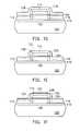
- FIGS. 1A through 1Fare schematic cross-sectional views showing the progression of steps for forming a polysilicon thin film transistor according to one preferred embodiment of this invention.
- FIGS. 1A through 1Fare schematic cross-sectional views showing the progression of steps for forming a polysilicon thin film transistor according to one preferred embodiment of this invention.
- an insulating substrate 100is provided.
- An amorphous silicon channel layer 102is formed over the insulating substrate 100 by, for example, chemical vapor deposition. Conventional photolithographic and etching processes are used to pattern out an active area in the amorphous silicon channel layer 102 .
- An oxide layer 104is formed over the amorphous silicon channel layer 102 .
- the oxide layer 104can be a silicon oxide layer formed, for example, by thermal oxidation.
- a conductive layer 106is formed over the oxide layer 104 .
- the conductive layer 106can be a polysilicon layer or a polysilicon-germanium layer formed, for example, by chemical vapor deposition.
- the conductive layer 106is patterned to form a gate electrode 108 .
- the gate electrode 108is formed, for example, by photolithographic and etching processes. Using the gate electrode 108 as a mask, a low-dopant-concentration implantation is carried out to form a lightly doped region in the amorphous silicon channel layer 102 .
- the lightly doped regionis a lightly doped source/drain region 110 formed, for example, by selectively implanting N ⁇ ions into the amorphous silicon channel layer 102 (indicated by arrows).
- a channel region 112is formed underneath the gate electrode 108 .
- conductive materialis selectively deposited over the gate electrode 108 to form a spacer 114 that completely encloses the gate electrode 108 .
- the spacer 114can be a polysilicon or a polysilicon-germanium layer formed, for example, by ultra-high-vacuum chemical vapor deposition (UHVCVD). Because polysilicon or polysilicon-germanium has a long incubation period over a silicon oxide layer but rapid deposition over a polysilicon layer, polysilicon or polysilicon germanium is selectively deposited over the gate electrode 108 . Alternatively, a chemical vapor deposition may be carried out to form a conductive material layer over the gate electrode and the oxide layer 104 .
- a high-dopant-concentration implantation of the amorphous silicon channel layer 102is conducted (indicated by arrows) while using the spacer-covered gate electrode 108 as a mask to form a heavily doped region on each side of the amorphous silicon channel layer 102 .
- the heavily doped regionis a source/drain region 116 formed, for example, by implanting N + ions selectively into the amorphous silicon channel layer 102 .
- the oxide layer 104 above the source/drain region 116is removed.
- the oxide layer 104is removed, for example, by wet etching using hydrofluoric acid as an etchant.
- An insulating layer 118is formed over the entire insulating substrate 100 .
- the insulation layer 118is a material layer that has a vastly different etching rate from the spacer 110 such as a silicon oxide layer or a silicon nitride layer.
- the insulation layer 118is formed, for example, by plasma-enhanced chemical vapor deposition (PECVD).
- a portion of the insulation layer 118is removed to form an isolation spacer 120 on the sidewall of the spacer 114 so that a top section 122 of the spacer 114 is exposed.
- the isolation spacer 120is formed, for example, by anisotropic etching.
- a self-aligned silicide layer 124is formed over the substrate 100 .
- the self-aligned silicide layer 124can be a nickel silicide layer, a tungsten silicide layer, a cobalt silicide layer, a titanium silicide layer, a platinum silicide layer or a palladium silicide layer, for example.
- the self-aligned silicide layer 124is formed, for example, by performing molecular beam evaporation or DC magnetron sputtering to form a refractory metal layer (not shown) having a thickness between about 200 ⁇ and 1000 ⁇ over the entire wafer.
- the refractory metal layeris formed using material such as nickel, tungsten, cobalt, titanium, platinum or palladium.
- a rapid thermal processis conducted so that a portion of the refractory metal reacts with the silicon at the top section 122 of the spacer 114 and the source/drain region 116 to form the self-aligned silicide layer 124 .
- the unreacted refractory metalis removed, for example, by wet etching using hydrochloric acid as an etchant.
- a metal-induced lateral crystallization processis conducted at a suitable temperature (for example, below 500° C. and preferably between about 300° C. and 500° C.) for a preset period.
- a suitable temperaturefor example, below 500° C. and preferably between about 300° C. and 500° C.
- lateral crystallization of the amorphous silicon channel layer 102is induced.
- a polysilicon channel layer 126(a metal-induced lateral crystallization polysilicon channel layer) and hence a complete polysilicon thin film transistor is formed.
- This inventionalso provides a polysilicon thin film transistor having a structure shown in FIG. 1F.
- the polysilicon thin film transistor structureincludes an insulating substrate 100 and a metal-induced lateral crystallization channel layer 126 above the insulating substrate 100 .
- the metal-induced lateral crystallization polysilicon channel layer 126further includes a channel region 112 , a lightly doped source/drain region 110 and a source/drain region 116 .
- the lightly doped source/drain region 110is adjacent to the channel region 112 and the source/drain region 116 is adjacent to the lightly doped source/drain region 110 .
- An oxide layer 104lies above the metal-induced lateral crystallization polysilicon channel layer 126 and covers both the channel region 112 and the lightly doped source/drain region 110 .
- a gate electrode 108is on oxide layer 104 inside the channel region 112 .
- a first spacer 114encloses the gate electrode 108 .
- a second spacer 120attaches to the sidewall of the first spacer 114 but exposes the top section of the first spacer 114 .
- a self-aligned metal silicide layer 124lies on the top section of the first spacer 114 and a portion of the exposed source/drain region 116 .
- this inventionprovides a polysilicon thin film transistor structure and corresponding method of manufacture.
- the structurereduces overall leakage current from various terminals of the transistor and lowers resistance of its source/drain terminals and gate electrode. Therefore, operating speed of the transistor is increased and production yield of the semiconductor devices is improved.
- polysilicon or polysilicon-germaniumcan be selectively deposited over a polysilicon layer so that a gate-covered lightly doped drain structure is directly formed.
- a chemical vapor depositionis conducted to deposit a layer of polysilicon or polysilicon-germanium followed by an anisotropic etching operation to remove a portion of the polysilicon or polysilicon-germanium layer.
- thickness of the spacercan be accurately controlled and a gate-covered lightly doped source/drain polysilicon thin film transistor can be easily fabricated. Ultimately, leakage current from the transistor is effectively lowered.
- metal silicide layerover the gate electrode and the source/drain terminals. Since metal silicide material has a resistance far lower than polysilicon, resistance at the gate electrode and the source/drain region is greatly lowered.
- the amorphous silicon channel layeris crystallized into a polysilicon channel having larger crystal grains.
- carrier mobility in the channelis increased and response speed of the transistor is improved.
Landscapes
- Thin Film Transistor (AREA)
Abstract
Description
- This application claims the priority benefit of Taiwan application serial no. 90109736, filed on Apr. 24, 2001.[0001]
- 1. Field of Invention[0002]
- The present invention relates to a method of manufacturing an integrated circuit device. More particularly, the present invention relates to a method of forming a polysilicon thin film transistor (poly-Si TFT) structure.[0003]
- 2. Description of Related Art[0004]
- Thin film transistors are often used in active matrix liquid-crystalline devices (AMLCD) and static random access memory (SRAM). A thin film transistor can be classified as belonging to an amorphous silicon thin film type or a polysilicon thin film type. A polysilicon thin film transistor is able to provide higher carrier mobility and higher conductive current than an amorphous silicon thin film transistor. Furthermore, a polysilicon thin film transistor can be directly used in a peripheral circuit for forming the logic drivers of a display device. Since the driver circuit and the thin film transistor array can be fabricated on the same glass panel with a reduction of production cost, polysilicon thin film transistors are frequently used in liquid crystal display (LCD) panels. However, polysilicon thin film transistors generally produce a relatively large leakage current. In addition, the polysilicon thin film transistors must be able to attain a certain speed before they can be considered suitable for applications in logic circuit. Therefore, polysilicon thin film transistors are rarely used in large area liquid crystal display. To be incorporated inside a large area liquid crystal display, leakage current from the polysilicon thin film transistor must be reduced and operating speed of the transistor must be increased.[0005]
- A major factor that may affect the amount of leakage current from a polysilicon thin film transistor includes the size of the electric field in the neighborhood of its drain terminal. To reduce leakage current, the electric field in the depletion region of a drain terminal must be reduced. The conventional method of reducing the electric field in the depletion region of a drain terminal is to produce a polysilicon thin film transistor with a lightly doped drain terminal or a gate-overlapped lightly doped drain.[0006]
- Although the production of a lightly doped region between the drain terminal and the gate terminal of a polysilicon thin film transistor is able to reduce electric field in the depletion region and hence leakage current, electrical resistance is increased considerably in the lightly doped region. Hence, the amount of conductive current permitted to pass through the device is reduced and the response speed of the device is greatly lowered when the device is conductive.[0007]
- In a polysilicon thin film transistor with a gate-overlapped lightly doped drain terminal, the lightly doped drain terminal is under the gate electrode so that the gate electrode and the lightly doped region overlap. In the conductive state, the gate electrode is able to sense the carriers in the lightly doped region, thereby lowering the resistance and maintaining a normal conductive current. In the non-conductive state, resistance is increased due to the expulsion of carriers from the lightly doped region by a gate voltage. Similarly, the electric field in the depletion region is lowered and leakage current is suppressed. However, in this type of structure, a highly conductive material such as polysilicon must be used to form the spacers. If, furthermore, metal silicide material is used to lower the resistance at a source/drain terminal, a conductive path is created between the gate electrode and the source/drain terminal. Hence, intrinsic properties of the device may be further damaged.[0008]
- On the other hand, a principle factor that affects the operating speed of a polysilicon thin film transistor includes defects at polysilicon grain boundaries. Defects in these grain boundaries tend to trap carriers and set up regional potential barriers. By increasing the size of grains so that the number of crystal boundaries crossed per unit length is decreased, response speed of the polysilicon thin film transistor will increase considerably. The conventional method of increasing the size of polysilicon crystals includes solid phase crystallization (SPC), laser re-crystallization and metal-induced lateral crystallization (MILC).[0009]
- To perform solid phase crystallization, a substrate with an amorphous silicon layer is placed inside a furnace. The furnace is heated to 600° C. and the amorphous silicon layer is treated for a period of 24 hours so that the amorphous silicon is transformed into polysilicon. However, the high temperature treatment limits the type of material that can be used to form the bottom glass panel of a liquid crystal display. Hence, the production cost of the liquid crystal display panel is increased.[0010]
- To perform a laser re-crystallization, a the amorphous silicon layer is scanned with a laser beam. Thermal energy produced by the laser beam re-crystallizes the amorphous silicon into polysilicon. Although re-crystallization temperature and defect density along the crystal boundaries are lowered, the polysilicon layer thus formed has a very rough surface which leads to intense dispersion at the interface between a polysilicon channel and a gate oxide layer. Ultimately, carrier mobility is greatly lowered. In addition, the polysilicon crystals resulting from laser re-crystallization are perpendicular to the channel and have a columnar form. Hence, size increase of crystals in a direction parallel to the channel is limited.[0011]
- Metal-induced lateral crystallization (MILC) is a method capable of producing crystal growth in a direction parallel to the channel. After the completion of a conventional cap gate and gate production process, a metallic layer (for example, a nickel layer) is formed over the source/drain terminal. The wafer is heated to a temperature of about 500° C. Utilizing the metal silicide above the source/drain terminal as a seed nucleus, crystals grow laterally from a source/drain region and extend into the channel region underneath the gate electrode. Under suitable growing conditions, lateral width of a crystal may be as long as[0012]10 μm and carriers rarely encounter a crystal boundary when traversing the channel. However, in the process of forming the lateral crystals, a large number of defects are also created at the interface between the metal-induced crystals and the metal-induced lateral crystal so that operating speed of the device is lowered. To remove the interface between the metal-induced crystals and the metal-induced lateral crystal from the channel region, a masking procedure can be carried out. However, this extra step will increase production cost.
- Accordingly, one object of the present invention is to provide a method of forming a polysilicon thin film transistor capable of reducing leakage current from the transistor and resistance at its source terminal, drain terminal and gate terminal. The method is further capable of improving the electrical properties of the transistor.[0013]
- A second object of the invention is to provide a method of forming a polysilicon thin film transistor capable of reducing carrier mobility drop and hence current drop due to the crystal boundary crossing of carriers. Hence, operating speed of the transistor is increased and electrical properties of the transistor are improved.[0014]
- A third object of the invention is to provide a method of forming a polysilicon thin film transistor having a double-layered spacer structure capable of suppressing leakage current and excluding its metal-induced crystal/metal-induced lateral crystal interface from its channel region at the same time. Although the interface contains more defects, the defect-ridden interface lies in the source/drain region without affecting any properties of the transistor.[0015]
- To achieve these and other advantages and in accordance with the purpose of the invention, as embodied and broadly described herein, the invention provides a method of forming a polysilicon thin film transistor. First, an insulating substrate is provided. An amorphous channel layer is formed over the substrate. Photolithographic and etching techniques are used to pattern out an active region in the amorphous silicon channel layer. An oxide layer and a conductive layer are sequentially formed over the amorphous silicon channel layer. The conductive layer is patterned to form a gate electrode. Thereafter, using the gate electrode as a mask, a lightly doped source/drain region is formed in the amorphous silicon channel layer. A spacer that encloses the gate electrode is formed. A source/drain region is formed in the amorphous silicon channel layer. Using the spacer and the gate electrode as a mask, a portion of the oxide layer above the source/drain terminal is removed. Hence, an isolation spacer is formed on the sidewalls of the original spacer while the top section of the original spacer is exposed. A self-aligned silicide layer is formed over the top section of the original spacer and the source/drain region. Finally, a metal-induced lateral crystallization process is conducted to transform the amorphous silicon channel layer into a lateral-crystallization-polysilicon channel layer.[0016]
- The spacer may be formed only on sidewalls of the gate electrode while exposing a top of the gate electrode, so that a self-aligned silicide is formed on the top of the gate electrode.[0017]
- This invention also provides a polysilicon thin film transistor structure. The structure includes an insulating substrate and a metal-induced lateral crystallization polysilicon channel layer above the substrate. The metal-induced lateral crystallization polysilicon channel layer further includes a channel region, a lightly doped source/drain region and a source/drain region. The lightly doped source/drain region is adjacent to the channel region and the source/drain region is adjacent to the lightly doped source/drain region. An oxide layer lies above the metal-induced lateral crystallization polysilicon channel layer and covers both the channel region and the lightly doped source/drain region. A gate electrode is on the oxide layer inside the channel region. A first spacer covers the gate electrode entirely. A second spacer attaches to the sidewall of the first spacer. A self-aligned metal silicide layer lies on the top section of the first spacer and a portion of the exposed source/drain region.[0018]
- The spacer may be formed only on sidewalls of the gate electrode while exposing a top of the gate electrode, so that a self-aligned silicide is formed on the top of the gate electrode.[0019]
- One major aspect of this invention is the utilization of double-layered spacer technique and metal-induced lateral crystallization technique to fabricate a polysilicon thin film transistor. The transistor so formed has a smaller leakage current and a faster operating speed. Further, the interface between metal-induced crystallization region and metal-induced lateral crystallization region is excluded from the channel area so that any defects in the interface will not affect any operating properties of the transistor.[0020]
- Leakage current from the transistor is greatly reduced by selectively depositing polysilicon or polysilicon-germanium material over the gate electrode to form a spacer that serves as a lightly doped drain structure over the gate electrode.[0021]
- In addition, the application of a self-aligned technique to form a metal silicide layer over the gate electrode and the source/drain region reduces overall resistance at the gate and the source/drain terminal.[0022]
- Furthermore, the metal silicide layer above the source/drain region is utilized to initiate a metal-induced lateral crystallization so that amorphous silicon within the channel layer is transformed into a lateral-crystallization-polysilicon channel layer. Ultimately, a channel with large crystals is produced and carrier mobility and hence operating speed is greatly increased. Moreover, the double-layered spacer structure permits the exclusion of the metal-induced crystallization/metal-induced lateral crystallization interface from the channel region. Although the interface may contain a great number of defects, the interface is located within the source/drain region. Hence, the transistor device is unaffected by such interface defects.[0023]
- It is to be understood that both the foregoing general description and the following detailed description are exemplary, and are intended to provide further explanation of the invention as claimed.[0024]
- The accompanying drawings are included to provide a further understanding of the invention, and are incorporated in and constitute a part of this specification. The drawings illustrate embodiments of the invention and, together with the description, serve to explain the principles of the invention. In the drawings,[0025]
- FIGS. 1A through 1F are schematic cross-sectional views showing the progression of steps for forming a polysilicon thin film transistor according to one preferred embodiment of this invention.[0026]
- Reference will now be made in detail to the present preferred embodiments of the invention, examples of which are illustrated in the accompanying drawings. Wherever possible, the same reference numbers are used in the drawings and the description to refer to the same or like parts.[0027]
- FIGS. 1A through 1F are schematic cross-sectional views showing the progression of steps for forming a polysilicon thin film transistor according to one preferred embodiment of this invention.[0028]
- As shown in FIG. 1A, an insulating[0029]
substrate 100 is provided. An amorphoussilicon channel layer 102 is formed over the insulatingsubstrate 100 by, for example, chemical vapor deposition. Conventional photolithographic and etching processes are used to pattern out an active area in the amorphoussilicon channel layer 102. Anoxide layer 104 is formed over the amorphoussilicon channel layer 102. Theoxide layer 104 can be a silicon oxide layer formed, for example, by thermal oxidation. Aconductive layer 106 is formed over theoxide layer 104. Theconductive layer 106 can be a polysilicon layer or a polysilicon-germanium layer formed, for example, by chemical vapor deposition. - As shown in FIG. 1B, the[0030]
conductive layer 106 is patterned to form agate electrode 108. Thegate electrode 108 is formed, for example, by photolithographic and etching processes. Using thegate electrode 108 as a mask, a low-dopant-concentration implantation is carried out to form a lightly doped region in the amorphoussilicon channel layer 102. The lightly doped region is a lightly doped source/drain region 110 formed, for example, by selectively implanting N− ions into the amorphous silicon channel layer102 (indicated by arrows). Achannel region 112 is formed underneath thegate electrode 108. - As shown in FIG. 1C, conductive material is selectively deposited over the[0031]
gate electrode 108 to form aspacer 114 that completely encloses thegate electrode 108. Thespacer 114 can be a polysilicon or a polysilicon-germanium layer formed, for example, by ultra-high-vacuum chemical vapor deposition (UHVCVD). Because polysilicon or polysilicon-germanium has a long incubation period over a silicon oxide layer but rapid deposition over a polysilicon layer, polysilicon or polysilicon germanium is selectively deposited over thegate electrode 108. Alternatively, a chemical vapor deposition may be carried out to form a conductive material layer over the gate electrode and theoxide layer 104. This is followed by performing an anisotropic etching to remove a portion of the conductive material. A high-dopant-concentration implantation of the amorphoussilicon channel layer 102 is conducted (indicated by arrows) while using the spacer-coveredgate electrode 108 as a mask to form a heavily doped region on each side of the amorphoussilicon channel layer 102. The heavily doped region is a source/drain region 116 formed, for example, by implanting N+ ions selectively into the amorphoussilicon channel layer 102. - As shown in FIG. 1D, the[0032]
oxide layer 104 above the source/drain region 116 is removed. Theoxide layer 104 is removed, for example, by wet etching using hydrofluoric acid as an etchant. An insulatinglayer 118 is formed over the entire insulatingsubstrate 100. Theinsulation layer 118 is a material layer that has a vastly different etching rate from thespacer 110 such as a silicon oxide layer or a silicon nitride layer. Theinsulation layer 118 is formed, for example, by plasma-enhanced chemical vapor deposition (PECVD). - As shown in FIG. 1E, a portion of the[0033]
insulation layer 118 is removed to form anisolation spacer 120 on the sidewall of thespacer 114 so that atop section 122 of thespacer 114 is exposed. Theisolation spacer 120 is formed, for example, by anisotropic etching. - As shown in FIG. 1F, a self-aligned[0034]
silicide layer 124 is formed over thesubstrate 100. The self-alignedsilicide layer 124 can be a nickel silicide layer, a tungsten silicide layer, a cobalt silicide layer, a titanium silicide layer, a platinum silicide layer or a palladium silicide layer, for example. The self-alignedsilicide layer 124 is formed, for example, by performing molecular beam evaporation or DC magnetron sputtering to form a refractory metal layer (not shown) having a thickness between about 200Å and 1000Å over the entire wafer. The refractory metal layer is formed using material such as nickel, tungsten, cobalt, titanium, platinum or palladium. A rapid thermal process is conducted so that a portion of the refractory metal reacts with the silicon at thetop section 122 of thespacer 114 and the source/drain region 116 to form the self-alignedsilicide layer 124. Thereafter, the unreacted refractory metal is removed, for example, by wet etching using hydrochloric acid as an etchant. - A metal-induced lateral crystallization process is conducted at a suitable temperature (for example, below 500° C. and preferably between about 300° C. and 500° C.) for a preset period. Using the self-aligned[0035]
silicide layer 124 above the source/drain region 116 as a seed nucleus, lateral crystallization of the amorphoussilicon channel layer 102 is induced. Ultimately, a polysilicon channel layer126 (a metal-induced lateral crystallization polysilicon channel layer) and hence a complete polysilicon thin film transistor is formed. - This invention also provides a polysilicon thin film transistor having a structure shown in FIG. 1F. The polysilicon thin film transistor structure includes an insulating[0036]
substrate 100 and a metal-induced lateralcrystallization channel layer 126 above the insulatingsubstrate 100. The metal-induced lateral crystallizationpolysilicon channel layer 126 further includes achannel region 112, a lightly doped source/drain region 110 and a source/drain region 116. The lightly doped source/drain region 110 is adjacent to thechannel region 112 and the source/drain region 116 is adjacent to the lightly doped source/drain region 110. Anoxide layer 104 lies above the metal-induced lateral crystallizationpolysilicon channel layer 126 and covers both thechannel region 112 and the lightly doped source/drain region 110. Agate electrode 108 is onoxide layer 104 inside thechannel region 112. Afirst spacer 114 encloses thegate electrode 108. Asecond spacer 120 attaches to the sidewall of thefirst spacer 114 but exposes the top section of thefirst spacer 114. A self-alignedmetal silicide layer 124 lies on the top section of thefirst spacer 114 and a portion of the exposed source/drain region 116. - In brief, this invention provides a polysilicon thin film transistor structure and corresponding method of manufacture. The structure reduces overall leakage current from various terminals of the transistor and lowers resistance of its source/drain terminals and gate electrode. Therefore, operating speed of the transistor is increased and production yield of the semiconductor devices is improved.[0037]
- In conclusion, major advantages of this invention include:[0038]
- 1. Utilizing the long incubation period of polysilicon or polysilicon-germanium material on a silicon oxide layer, polysilicon or polysilicon-germanium can be selectively deposited over a polysilicon layer so that a gate-covered lightly doped drain structure is directly formed. Alternatively, a chemical vapor deposition is conducted to deposit a layer of polysilicon or polysilicon-germanium followed by an anisotropic etching operation to remove a portion of the polysilicon or polysilicon-germanium layer. Hence, thickness of the spacer can be accurately controlled and a gate-covered lightly doped source/drain polysilicon thin film transistor can be easily fabricated. Ultimately, leakage current from the transistor is effectively lowered.[0039]
- 2. Self-aligned technique is used to form a metal silicide layer over the gate electrode and the source/drain terminals. Since metal silicide material has a resistance far lower than polysilicon, resistance at the gate electrode and the source/drain region is greatly lowered.[0040]
- 3. Using the metal silicide material above the source/drain region to induce lateral crystallization, the amorphous silicon channel layer is crystallized into a polysilicon channel having larger crystal grains. Thus, carrier mobility in the channel is increased and response speed of the transistor is improved.[0041]
- 4. Using a double-spacer structure, leakage current from the transistor is suppressed. Moreover, the metal-induced crystallization/metal-induced lateral crystallization interface is excluded from the effective channel region. Although the interface may contain many defects, these defects will not affect the electrical properties of the transistor because the interface lies in the source/drain region.[0042]
- It will be apparent to those skilled in the art that various modifications and variations can be made to the structure of the present invention without departing from the scope or spirit of the invention. In view of the foregoing, it is intended that the present invention cover modifications and variations of this invention provided they fall within the scope of the following claims and their equivalents.[0043]
Claims (22)
1. A method of forming polysilicon thin film transistor, comprising:
providing an insulating substrate;
forming an amorphous silicon channel layer over the substrate;
patterning out an active region in the amorphous silicon channel layer by applying photolithographic and etching processes;
forming an oxide layer over the amorphous silicon channel layer;
forming a conductive layer over the oxide layer;
patterning the conductive layer to form a gate electrode;
forming a lightly doped source/drain region in the amorphous silicon channel layer while using the gate electrode as a mask;
performing a selective deposition of conductive material over the gate electrode to form a spacer that encloses the gate electrode;
forming a source/drain region in the amorphous silicon channel layer while using the spacer and the gate electrode as a mask;
removing a portion of the oxide layer over the source/drain region;
forming an isolation spacer on a sidewall of the spacer but exposing a top section of the spacer;
forming a self-aligned silicide layer over the source/drain region and the top section of the spacer; and
performing a metal-induced lateral crystallization process so that the amorphous silicon channel layer is transformed into a metal-induced lateral crystallization polysilicon channel layer.
2. The method ofclaim 1 , wherein the metal-induced lateral crystallization process is carried out at a temperature below about 500° C.
3. The method ofclaim 1 , wherein the spacer comprises polysilicon or polysilicon-germanium.
4. The method ofclaim 1 , wherein forming the spacer includes performing an ultra-high-vacuum chemical vapor deposition.
5. The method ofclaim 1 , wherein the gate electrode comprises polysilicon-germanium or polysilicon.
6. The method ofclaim 1 , wherein forming the isolation spacer further includes:
depositing insulation material over the substrate; and
performing an anisotropic etching operation to remove a portion of the insulation layer.
7. The method ofclaim 1 , wherein the insulation layer comprises silicon oxide or silicon nitride.
8. The method ofclaim 1 , wherein the self-aligned silicide layer is made from a material selected from a group consisting of nickel silicide, tungsten silicide, cobalt silicide, titanium silicide, platinum silicide and palladium silicide.
9. The method ofclaim 8 , wherein forming the silicide layer over the gate electrode and the source/drain region further includes:
forming a metallic layer over the insulating substrate;
performing a rapid thermal process so that metal in the metallic layer reacts with silicon in the source/drain region and the top section of the spacer; and
removing any unreacted metal.
10. The method ofclaim 9 , wherein the metal layer is made from a material selected from a group consisting of nickel, tungsten, cobalt, titanium, platinum and palladium.
11. A method of forming a polysilicon thin film transistor, comprising:
providing an insulating substrate having an amorphous silicon channel layer, an oxide layer and a conductive layer thereon;
patterning the conductive layer to form a gate electrode;
forming a lightly doped source/drain region in the amorphous silicon channel layer while using the gate electrode as a mask;
forming a conductive material layer over the insulating substrate;
removing a portion of the conductive material to form a first spacer on a sidewall of the gate electrode;
forming a source/drain region in the amorphous silicon channel layer while using the first spacer and the gate electrode as a mask;
removing a portion of the oxide layer above the source/drain region;
forming an insulating layer over the insulating substrate;
removing a portion of the insulating layer to form a second spacer on a sidewall of the first spacer but exposing a top of the gate electrode;
forming a metallic layer over the insulating substrate;
performing a rapid thermal process so that metal in the metallic layer reacts with silicon in the source/drain region and silicon at the top section of the gate electrode to form a self-aligned silicide layer;
removing any unreacted metal; and
performing a metal-induced lateral crystallization process so that the amorphous silicon channel layer is transformed into a metal-induced lateral crystallization polysilicon channel layer.
12. The method ofclaim 11 , wherein the metal-induced lateral crystallization process is carried out at a temperature below about 500° C.
13. The method ofclaim 11 , wherein the conductive layer comprises polysilicon or polysilicon-germanium.
14. The method ofclaim 11 , wherein forming the first spacer includes performing an anisotropic etching.
15. The method ofclaim 11 , wherein material constituting the insulation layer includes silicon oxide or silicon nitride.
16. The method ofclaim 11 , wherein forming the second spacer includes performing an anisotropic etching process.
17. A polysilicon thin film transistor structure, comprising:
an insulating substrate;
a metal-induced lateral crystallization polysilicon channel layer above the insulating substrate, wherein the metal-induced lateral crystallization polysilicon channel layer includes a channel region, a lightly doped source/drain region and a source/drain region, the lightly doped source/drain region is adjacent to the channel region and the source/drain region is adjacent to the lightly doped source/drain region;
an oxide layer above the metal-induced lateral crystallization polysilicon channel layer and covering the channel region and the lightly doped source/drain region;
a gate electrode above the oxide layer within the channel region;
a spacer over the gate electrode and sidewalls of the gate electrode;
an isolation spacer on sidewalls of the spacer; and
a self-aligned silicide layer over the top of the gate electrode and an exposed portion of the source/drain region.
18. The structure ofclaim 17 , wherein the gate electrode comprises polysilicon-germanium or polysilicon.
19. The structure ofclaim 17 , wherein the spacer comprises polysilicon-germanium or polysilicon.
20. The structure ofclaim 17 , wherein the oxide layer includes a silicon oxide layer.
21. The structure ofclaim 17 , wherein the isolation spacer comprises silicon oxide or silicon nitride.
22. The structure ofclaim 17 , wherein the self-aligned silicide layer is made of a material selected from a group consisting of nickel silicide, tungsten silicide, cobalt silicide, titanium silicide, platinum silicide and palladium silicide.
Priority Applications (1)
| Application Number | Priority Date | Filing Date | Title |
|---|---|---|---|
| US09/994,322US6486496B2 (en) | 2001-04-24 | 2001-11-26 | Polysilicon thin film transistor structure |
Applications Claiming Priority (5)
| Application Number | Priority Date | Filing Date | Title |
|---|---|---|---|
| TW090109736ATW480735B (en) | 2001-04-24 | 2001-04-24 | Structure and manufacturing method of polysilicon thin film transistor |
| TW90109736A | 2001-04-24 | ||
| TW90109736 | 2001-04-24 | ||
| US09/845,438US6410373B1 (en) | 2001-04-24 | 2001-04-30 | Method of forming polysilicon thin film transistor structure |
| US09/994,322US6486496B2 (en) | 2001-04-24 | 2001-11-26 | Polysilicon thin film transistor structure |
Related Parent Applications (1)
| Application Number | Title | Priority Date | Filing Date |
|---|---|---|---|
| US09/845,438DivisionUS6410373B1 (en) | 2001-04-24 | 2001-04-30 | Method of forming polysilicon thin film transistor structure |
Publications (2)
| Publication Number | Publication Date |
|---|---|
| US20020153527A1true US20020153527A1 (en) | 2002-10-24 |
| US6486496B2 US6486496B2 (en) | 2002-11-26 |
Family
ID=21678047
Family Applications (2)
| Application Number | Title | Priority Date | Filing Date |
|---|---|---|---|
| US09/845,438Expired - LifetimeUS6410373B1 (en) | 2001-04-24 | 2001-04-30 | Method of forming polysilicon thin film transistor structure |
| US09/994,322Expired - LifetimeUS6486496B2 (en) | 2001-04-24 | 2001-11-26 | Polysilicon thin film transistor structure |
Family Applications Before (1)
| Application Number | Title | Priority Date | Filing Date |
|---|---|---|---|
| US09/845,438Expired - LifetimeUS6410373B1 (en) | 2001-04-24 | 2001-04-30 | Method of forming polysilicon thin film transistor structure |
Country Status (2)
| Country | Link |
|---|---|
| US (2) | US6410373B1 (en) |
| TW (1) | TW480735B (en) |
Cited By (7)
| Publication number | Priority date | Publication date | Assignee | Title |
|---|---|---|---|---|
| US20020121639A1 (en)* | 2001-03-02 | 2002-09-05 | So Woo Young | Thin film transistor and manufacturing method thereof, and active matrix display device and manufacturing method thereof |
| US6586287B2 (en)* | 2001-03-30 | 2003-07-01 | Seung Ki Joo | Method for fabricating thin film transistor including crystalline silicon active layer |
| WO2004059717A1 (en)* | 2002-12-24 | 2004-07-15 | Koninklijke Philips Electronics N.V. | Thin film transistor, method for producing a thin film transistor and electronic device having such a transistor |
| US20060108636A1 (en)* | 2004-11-10 | 2006-05-25 | Canon Kabushiki Kaisha | Amorphous oxide and field effect transistor |
| US20070045849A1 (en)* | 2005-08-31 | 2007-03-01 | Taiwan Semiconductor Manufacturing Company, Ltd. | Semiconductor structure having selective silicide-induced stress and a method of producing same |
| US20070072350A1 (en)* | 2001-01-26 | 2007-03-29 | Semiconductor Energy Laboratory Co., Ltd. | Method of manufacturing semiconductor device |
| US20070298600A1 (en)* | 2006-06-22 | 2007-12-27 | Suh Bong-Seok | Method of Fabricating Semiconductor Device and Semiconductor Device Fabricated Thereby |
Families Citing this family (45)
| Publication number | Priority date | Publication date | Assignee | Title |
|---|---|---|---|---|
| TW297142B (en)* | 1993-09-20 | 1997-02-01 | Handotai Energy Kenkyusho Kk | |
| US6555449B1 (en) | 1996-05-28 | 2003-04-29 | Trustees Of Columbia University In The City Of New York | Methods for producing uniform large-grained and grain boundary location manipulated polycrystalline thin film semiconductors using sequential lateral solidfication |
| US6830993B1 (en)* | 2000-03-21 | 2004-12-14 | The Trustees Of Columbia University In The City Of New York | Surface planarization of thin silicon films during and after processing by the sequential lateral solidification method |
| KR100854834B1 (en) | 2000-10-10 | 2008-08-27 | 더 트러스티스 오브 컬럼비아 유니버시티 인 더 시티 오브 뉴욕 | Method and apparatus for processing thin metal layers |
| TW552645B (en)* | 2001-08-03 | 2003-09-11 | Semiconductor Energy Lab | Laser irradiating device, laser irradiating method and manufacturing method of semiconductor device |
| JP4397571B2 (en) | 2001-09-25 | 2010-01-13 | 株式会社半導体エネルギー研究所 | Laser irradiation method, laser irradiation apparatus, and manufacturing method of semiconductor device |
| KR100436067B1 (en)* | 2001-11-16 | 2004-06-12 | 주식회사 하이닉스반도체 | Image sensor and method of fabricating the same |
| WO2004017380A2 (en) | 2002-08-19 | 2004-02-26 | The Trustees Of Columbia University In The City Of New York | A single-shot semiconductor processing system and method having various irradiation patterns |
| KR101131040B1 (en) | 2002-08-19 | 2012-03-30 | 더 트러스티스 오브 콜롬비아 유니버시티 인 더 시티 오브 뉴욕 | Process and system for laser crystallization processing of film regions on a substrate to minimize edge areas, and structure of such film regions |
| US6909145B2 (en)* | 2002-09-23 | 2005-06-21 | International Business Machines Corporation | Metal spacer gate for CMOS FET |
| WO2004075263A2 (en) | 2003-02-19 | 2004-09-02 | The Trustees Of Columbia University In The City Of New York | System and process for processing a plurality of semiconductor thin films which are crystallized using sequential lateral solidification techniques |
| US7238963B2 (en)* | 2003-04-28 | 2007-07-03 | Tpo Displays Corp. | Self-aligned LDD thin-film transistor and method of fabricating the same |
| CN1301538C (en)* | 2003-05-28 | 2007-02-21 | 统宝光电股份有限公司 | Thin film transistor structure and manufacturing method thereof |
| US7364952B2 (en)* | 2003-09-16 | 2008-04-29 | The Trustees Of Columbia University In The City Of New York | Systems and methods for processing thin films |
| TWI351713B (en) | 2003-09-16 | 2011-11-01 | Univ Columbia | Method and system for providing a single-scan, con |
| US7164152B2 (en) | 2003-09-16 | 2007-01-16 | The Trustees Of Columbia University In The City Of New York | Laser-irradiated thin films having variable thickness |
| WO2005029546A2 (en) | 2003-09-16 | 2005-03-31 | The Trustees Of Columbia University In The City Of New York | Method and system for providing a continuous motion sequential lateral solidification for reducing or eliminating artifacts, and a mask for facilitating such artifact reduction/elimination |
| TWI359441B (en) | 2003-09-16 | 2012-03-01 | Univ Columbia | Processes and systems for laser crystallization pr |
| WO2005029547A2 (en)* | 2003-09-16 | 2005-03-31 | The Trustees Of Columbia University In The City Of New York | Enhancing the width of polycrystalline grains with mask |
| US7318866B2 (en) | 2003-09-16 | 2008-01-15 | The Trustees Of Columbia University In The City Of New York | Systems and methods for inducing crystallization of thin films using multiple optical paths |
| WO2005034193A2 (en) | 2003-09-19 | 2005-04-14 | The Trustees Of Columbia University In The City Ofnew York | Single scan irradiation for crystallization of thin films |
| US20050074914A1 (en)* | 2003-10-06 | 2005-04-07 | Toppoly Optoelectronics Corp. | Semiconductor device and method of fabrication the same |
| US7202143B1 (en) | 2003-10-23 | 2007-04-10 | The Board Of Trustees Of The University Of Arkansas | Low temperature production of large-grain polycrystalline semiconductors |
| US20050258488A1 (en)* | 2004-04-27 | 2005-11-24 | Toppoly Optoelectronics Corp. | Serially connected thin film transistors and fabrication methods thereof |
| CN1331194C (en)* | 2004-06-30 | 2007-08-08 | 吉林大学 | A method for making metal induced polysilicon film having diffuse layer above metal |
| US7645337B2 (en)* | 2004-11-18 | 2010-01-12 | The Trustees Of Columbia University In The City Of New York | Systems and methods for creating crystallographic-orientation controlled poly-silicon films |
| JP2006269808A (en) | 2005-03-24 | 2006-10-05 | Mitsubishi Electric Corp | Semiconductor device and image display device |
| US8221544B2 (en) | 2005-04-06 | 2012-07-17 | The Trustees Of Columbia University In The City Of New York | Line scan sequential lateral solidification of thin films |
| US7867791B2 (en)* | 2005-07-29 | 2011-01-11 | Semiconductor Energy Laboratory Co., Ltd. | Manufacturing method of semiconductor device using multiple mask layers formed through use of an exposure mask that transmits light at a plurality of intensities |
| US8598588B2 (en) | 2005-12-05 | 2013-12-03 | The Trustees Of Columbia University In The City Of New York | Systems and methods for processing a film, and thin films |
| JP5110079B2 (en)* | 2007-03-16 | 2012-12-26 | 富士通セミコンダクター株式会社 | Manufacturing method of semiconductor device |
| TW200913269A (en)* | 2007-09-03 | 2009-03-16 | Chunghwa Picture Tubes Ltd | Thin film transistor and manufacturing method thereof |
| TW200942935A (en) | 2007-09-21 | 2009-10-16 | Univ Columbia | Collections of laterally crystallized semiconductor islands for use in thin film transistors and systems and methods for making same |
| JP5385289B2 (en) | 2007-09-25 | 2014-01-08 | ザ トラスティーズ オブ コロンビア ユニヴァーシティ イン ザ シティ オブ ニューヨーク | Method for producing high uniformity in thin film transistor devices fabricated on laterally crystallized thin films |
| US8012861B2 (en) | 2007-11-21 | 2011-09-06 | The Trustees Of Columbia University In The City Of New York | Systems and methods for preparing epitaxially textured polycrystalline films |
| WO2009067687A1 (en) | 2007-11-21 | 2009-05-28 | The Trustees Of Columbia University In The City Of New York | Systems and methods for preparation of epitaxially textured thick films |
| WO2009067688A1 (en) | 2007-11-21 | 2009-05-28 | The Trustees Of Columbia University In The City Of New York | Systems and methods for preparing epitaxially textured polycrystalline films |
| US8569155B2 (en) | 2008-02-29 | 2013-10-29 | The Trustees Of Columbia University In The City Of New York | Flash lamp annealing crystallization for large area thin films |
| JP2012508985A (en) | 2008-11-14 | 2012-04-12 | ザ トラスティーズ オブ コロンビア ユニヴァーシティ イン ザ シティ オブ ニューヨーク | System and method for thin film crystallization |
| US9087696B2 (en) | 2009-11-03 | 2015-07-21 | The Trustees Of Columbia University In The City Of New York | Systems and methods for non-periodic pulse partial melt film processing |
| US9646831B2 (en) | 2009-11-03 | 2017-05-09 | The Trustees Of Columbia University In The City Of New York | Advanced excimer laser annealing for thin films |
| US8440581B2 (en) | 2009-11-24 | 2013-05-14 | The Trustees Of Columbia University In The City Of New York | Systems and methods for non-periodic pulse sequential lateral solidification |
| JP2017143135A (en)* | 2016-02-09 | 2017-08-17 | 株式会社ジャパンディスプレイ | Thin film transistor |
| CN108122992B (en)* | 2016-11-28 | 2020-04-17 | 昆山工研院新型平板显示技术中心有限公司 | Channel layer structure and preparation method thereof, and thin film transistor device and preparation method thereof |
| US11227955B2 (en)* | 2019-09-22 | 2022-01-18 | Taiwan Semiconductor Manufacturing Company, Ltd. | Semiconductor device and method of manufacturing the same |
Family Cites Families (13)
| Publication number | Priority date | Publication date | Assignee | Title |
|---|---|---|---|---|
| JP2794678B2 (en)* | 1991-08-26 | 1998-09-10 | 株式会社 半導体エネルギー研究所 | Insulated gate semiconductor device and method of manufacturing the same |
| KR960012583B1 (en)* | 1993-06-21 | 1996-09-23 | Lg Semicon Co Ltd | Tft (thin film transistor )and the method of manufacturing the same |
| US5416043A (en)* | 1993-07-12 | 1995-05-16 | Peregrine Semiconductor Corporation | Minimum charge FET fabricated on an ultrathin silicon on sapphire wafer |
| JPH07321323A (en)* | 1994-05-24 | 1995-12-08 | Matsushita Electric Ind Co Ltd | Thin film transistor and manufacturing method thereof |
| US5915174A (en)* | 1994-09-30 | 1999-06-22 | Semiconductor Energy Laboratory Co., Ltd. | Semiconductor device and method for producing the same |
| KR100229678B1 (en)* | 1996-12-06 | 1999-11-15 | 구자홍 | Thin film transistor and its manufacturing method |
| US6140684A (en)* | 1997-06-24 | 2000-10-31 | Stmicroelectronic, Inc. | SRAM cell structure with dielectric sidewall spacers and drain and channel regions defined along sidewall spacers |
| US6277679B1 (en)* | 1998-11-25 | 2001-08-21 | Semiconductor Energy Laboratory Co., Ltd. | Method of manufacturing thin film transistor |
| JP2000174282A (en)* | 1998-12-03 | 2000-06-23 | Semiconductor Energy Lab Co Ltd | Semiconductor device |
| US6259138B1 (en)* | 1998-12-18 | 2001-07-10 | Semiconductor Energy Laboratory Co., Ltd. | Semiconductor device having multilayered gate electrode and impurity regions overlapping therewith |
| US6653657B2 (en)* | 1999-12-10 | 2003-11-25 | Semoconductor Energy Laboratory Co., Ltd. | Semiconductor device and a method of manufacturing the same |
| TWI301907B (en)* | 2000-04-03 | 2008-10-11 | Semiconductor Energy Lab | Semiconductor device, liquid crystal display device and manfacturing method thereof |
| US6306721B1 (en)* | 2001-03-16 | 2001-10-23 | Chartered Semiconductor Maufacturing Ltd. | Method of forming salicided poly to metal capacitor |
- 2001
- 2001-04-24TWTW090109736Apatent/TW480735B/ennot_activeIP Right Cessation
- 2001-04-30USUS09/845,438patent/US6410373B1/ennot_activeExpired - Lifetime
- 2001-11-26USUS09/994,322patent/US6486496B2/ennot_activeExpired - Lifetime
Cited By (16)
| Publication number | Priority date | Publication date | Assignee | Title |
|---|---|---|---|---|
| US20070072350A1 (en)* | 2001-01-26 | 2007-03-29 | Semiconductor Energy Laboratory Co., Ltd. | Method of manufacturing semiconductor device |
| US7361577B2 (en)* | 2001-01-26 | 2008-04-22 | Semiconductor Energy Laboratory Co., Ltd. | Method of manufacturing semiconductor device |
| US20020121639A1 (en)* | 2001-03-02 | 2002-09-05 | So Woo Young | Thin film transistor and manufacturing method thereof, and active matrix display device and manufacturing method thereof |
| US7488982B2 (en)* | 2001-03-02 | 2009-02-10 | Samsung Mobile Display Co., Ltd. | Thin film transistor and manufacturing method thereof, and active matrix display device and manufacturing method thereof |
| US6586287B2 (en)* | 2001-03-30 | 2003-07-01 | Seung Ki Joo | Method for fabricating thin film transistor including crystalline silicon active layer |
| US20060040432A1 (en)* | 2002-12-24 | 2006-02-23 | Koninklijke Philips Electronics N.V. | Thin film trnsistor, method for producing a thin film transistor and electronic device having such a transistor |
| JP2006512756A (en)* | 2002-12-24 | 2006-04-13 | コーニンクレッカ フィリップス エレクトロニクス エヌ ヴィ | THIN FILM TRANSISTOR, METHOD FOR PRODUCING THIN FILM TRANSISTOR AND ELECTRONIC DEVICE PROVIDED WITH THIS TRANSISTOR |
| WO2004059717A1 (en)* | 2002-12-24 | 2004-07-15 | Koninklijke Philips Electronics N.V. | Thin film transistor, method for producing a thin film transistor and electronic device having such a transistor |
| US10615287B2 (en) | 2004-11-10 | 2020-04-07 | Canon Kabushiki Kaisha | Amorphous oxide and field effect transistor |
| US20060108636A1 (en)* | 2004-11-10 | 2006-05-25 | Canon Kabushiki Kaisha | Amorphous oxide and field effect transistor |
| US9583637B2 (en) | 2004-11-10 | 2017-02-28 | Canon Kabushiki Kaisha | Amorphous oxide and field effect transistor |
| US9130049B2 (en) | 2004-11-10 | 2015-09-08 | Canon Kabushiki Kaisha | Amorphous oxide and field effect transistor |
| US7601984B2 (en)* | 2004-11-10 | 2009-10-13 | Canon Kabushiki Kaisha | Field effect transistor with amorphous oxide active layer containing microcrystals and gate electrode opposed to active layer through gate insulator |
| US7875959B2 (en)* | 2005-08-31 | 2011-01-25 | Taiwan Semiconductor Manufacturing Company, Ltd. | Semiconductor structure having selective silicide-induced stress and a method of producing same |
| US20070045849A1 (en)* | 2005-08-31 | 2007-03-01 | Taiwan Semiconductor Manufacturing Company, Ltd. | Semiconductor structure having selective silicide-induced stress and a method of producing same |
| US20070298600A1 (en)* | 2006-06-22 | 2007-12-27 | Suh Bong-Seok | Method of Fabricating Semiconductor Device and Semiconductor Device Fabricated Thereby |
Also Published As
| Publication number | Publication date |
|---|---|
| US6486496B2 (en) | 2002-11-26 |
| TW480735B (en) | 2002-03-21 |
| US6410373B1 (en) | 2002-06-25 |
Similar Documents
| Publication | Publication Date | Title |
|---|---|---|
| US6410373B1 (en) | Method of forming polysilicon thin film transistor structure | |
| US6492213B1 (en) | Semiconductor device, thin film transistor and method for producing the same, and liquid crystal display apparatus and method for producing the same | |
| US6500736B2 (en) | Crystallization method of amorphous silicon | |
| US6531348B2 (en) | Method for crystallizing amorphous silicon and fabricating thin film transistor using crystallized silicon | |
| KR100333275B1 (en) | TFT of LCD device and the same methode | |
| US6861300B2 (en) | Fabricating method of polysilicon thin film transistor having a space and a plurality of channels | |
| EP0646950B1 (en) | Method for processing a thin film | |
| US7435667B2 (en) | Method of controlling polysilicon crystallization | |
| US7863621B2 (en) | Thin film transistor | |
| US6316294B1 (en) | Thin film transistor and a fabricating method thereof | |
| US20060049428A1 (en) | Tft electronic devices and their manufacture | |
| KR100303711B1 (en) | Thin film transistor with polycrystalline/amorphous double active layers | |
| KR100504538B1 (en) | Method For Crystallizing Amorphous Layer And Method For Fabricating Liquid Crystal Display Device By Using Said Method | |
| KR100470021B1 (en) | Method for crystallizing of silicon and method for fabricating of Thin film transistor | |
| JP3942100B2 (en) | Laser recrystallization method of low temperature polycrystalline silicon thin film transistor active layer | |
| US20060172469A1 (en) | Method of fabricating a polycrystalline silicon thin film transistor | |
| JPH07273338A (en) | Semiconductor device and manufacturing method thereof | |
| KR100751315B1 (en) | Thin film transistor, manufacturing method of thin film transistor and flat panel display device having same | |
| KR20070043393A (en) | Crystallization Method of Amorphous Silicon Thin Film and Manufacturing Method of Thin Film Transistor | |
| JP3859516B2 (en) | Manufacturing method of semiconductor device | |
| KR100709282B1 (en) | Thin film transistor and manufacturing method | |
| US7014708B2 (en) | Method of forming a thin film transistor by utilizing a laser crystallization process | |
| KR101018271B1 (en) | Method for manufacturing polycrystalline silicon thin film transistor | |
| KR20050016960A (en) | Tft electronic devices and their manufacture | |
| JPH08186262A (en) | Method for manufacturing thin film transistor |
Legal Events
| Date | Code | Title | Description |
|---|---|---|---|
| STCF | Information on status: patent grant | Free format text:PATENTED CASE | |
| FPAY | Fee payment | Year of fee payment:4 | |
| FPAY | Fee payment | Year of fee payment:8 | |
| AS | Assignment | Owner name:UNITED MICROELECTRONICS CORP., TAIWAN Free format text:ASSIGNMENT OF ASSIGNORS INTEREST;ASSIGNORS:CHANG, TING-CHANG;ZAN, HSIAO-WEN;SHIH, PO-SHENG;REEL/FRAME:026373/0885 Effective date:20010425 | |
| AS | Assignment | Owner name:INTELLECTUAL VENTURES FUND 74 LLC, NEVADA Free format text:ASSIGNMENT OF ASSIGNORS INTEREST;ASSIGNOR:UNITED MICROELECTRONICS CORP.;REEL/FRAME:026605/0333 Effective date:20110408 | |
| FPAY | Fee payment | Year of fee payment:12 | |
| AS | Assignment | Owner name:INTELLECTUAL VENTURES HOLDING 81 LLC, NEVADA Free format text:MERGER;ASSIGNOR:INTELLECTUAL VENTURES FUND 74 LLC;REEL/FRAME:037625/0564 Effective date:20150827 |