US20020152449A1 - Generating an instance-based representation of a design hierarchy - Google Patents
Generating an instance-based representation of a design hierarchyDownload PDFInfo
- Publication number
- US20020152449A1 US20020152449A1US09/835,313US83531301AUS2002152449A1US 20020152449 A1US20020152449 A1US 20020152449A1US 83531301 AUS83531301 AUS 83531301AUS 2002152449 A1US2002152449 A1US 2002152449A1
- Authority
- US
- United States
- Prior art keywords
- node
- layout
- instance
- design hierarchy
- cell
- Prior art date
- Legal status (The legal status is an assumption and is not a legal conclusion. Google has not performed a legal analysis and makes no representation as to the accuracy of the status listed.)
- Granted
Links
Images


Classifications
- G—PHYSICS
- G06—COMPUTING OR CALCULATING; COUNTING
- G06F—ELECTRIC DIGITAL DATA PROCESSING
- G06F30/00—Computer-aided design [CAD]
- G06F30/30—Circuit design
- G06F30/39—Circuit design at the physical level
- G06F30/398—Design verification or optimisation, e.g. using design rule check [DRC], layout versus schematics [LVS] or finite element methods [FEM]
Definitions
- This lightis generally reduced and focussed through an optical system that contains a number of lenses, filters and mirrors.
- the lightpasses through the clear regions of the mask and exposes the underlying photoresist layer.
- the lightis blocked by opaque regions of mask, leaving underlying portions of the photoresist layer unexposed.
- the exposed photoresist layeris then developed, typically through chemical removal of the exposed/non-exposed regions of the photoresist layer.
- the end resultis a semiconductor wafer with a photoresist layer having a desired pattern. This pattern can then be used for etching underlying regions of the wafer.
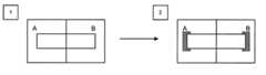
- FIGS. 3A, 3B and 3 Cillustrate how a layout, T, can be composed of a sub-cell A and a sub-cell B, wherein the sub-cell A further includes a sub-cell C.
- FIG. 3Aillustrates a nodal representation of this hierarchy and
- FIG. 3Billustrates a corresponding graphical representation.
- the systemdetermines how interactions with the node's siblings and/or parent, and possibly with other surrounding geometries, change the layout of the node as specified by the first cell. If the changes result in a new node for which no instance has been created, the system creates a new instance for the node.
- the environmental attributes specified by the parent of the nodeinclude geometrical features to be added to the node and to the node's siblings.
- FIG. 3Cillustrates a hierarchical representation of the layout in code form.
- FIG. 7Billustrates a modified design hierarchy for a layout in accordance with an embodiment of the invention. It is convenient to use this modified representation in generating the instance-based representation of the layout because the modified representation allows each node to encapsulate environmental information from its parent node as well as neighboring nodes.
- the systemadditionally determines whether the IB representation will reduce analysis effort below a threshold value (step 814 ). If so, the system performs an analysis, such as OPC, on the layout using the IB representation (step 816 ). Otherwise, the system performs the analysis on the layout using another representation, e.g. a flat, non-hierarchical, representation (step 818 ).
- an analysissuch as OPC
- the systemcreates two instances of cell A.
- the first instance A 710includes the effects of geometrical feature 902 and neighboring cell A 720 .
- the second instance A 720includes the effects of geometrical feature 904 and neighboring cell A 710 .
- cell A 710which appears at the bottom of FIG. 9, includes cells C 740 and D 750 in addition to geometrical feature 922 .
- geometrical feature 922affects the layout of cell C 740 .
- cell C 740can affect the layout of neighboring cell D 750
- cell D 750can affect the layout of neighboring cell C 740 .
- Thiscauses the system to create an instance of the cell C 740 that includes the effects of geometrical feature 922 and neighboring cell D 750 .
- Thisis the only instance created for cell C 740 because the other instance of cell C 760 under cell A 720 is the same as the instance of cell C 740 under cell A 710 .
- the systemalso creates an instance of the cell D 750 that includes the effects of neighboring cell C 740 .
Landscapes
- Engineering & Computer Science (AREA)
- Computer Hardware Design (AREA)
- Physics & Mathematics (AREA)
- Theoretical Computer Science (AREA)
- Evolutionary Computation (AREA)
- Geometry (AREA)
- General Engineering & Computer Science (AREA)
- General Physics & Mathematics (AREA)
- Design And Manufacture Of Integrated Circuits (AREA)
Abstract
Description
- 1. Field of the Invention[0001]
- The invention relates to the process of designing an integrated circuit. More specifically, the invention relates to a method and an apparatus for generating an instance-based representation of a set of geometrical features that comprise a layout of a circuit on a semiconductor chip in order to speed up subsequent operations on the layout.[0002]
- 2. Related Art[0003]
- Recent advances in integrated circuit technology have largely been accomplished by decreasing the feature size of circuit elements on a semiconductor chip. As the feature size of these circuit elements continues to decrease, circuit designers are forced to deal with problems that arise as a consequence of the optical lithography process that is typically used to manufacture integrated circuits. This optical lithography process generally begins with the formation of a photoresist layer on the surface of a semiconductor wafer. A mask composed of opaque regions, which are generally formed of chrome, and light-transmissive clear regions, which are generally formed of quartz, is then positioned over this photo resist layer coated wafer. (Note that the term “mask” as used in this specification is meant to include the term “retical.”) Light is then shone on the mask from a visible light source or an ultraviolet light source.[0004]
- This light is generally reduced and focussed through an optical system that contains a number of lenses, filters and mirrors. The light passes through the clear regions of the mask and exposes the underlying photoresist layer. At the same time, the light is blocked by opaque regions of mask, leaving underlying portions of the photoresist layer unexposed.[0005]
- The exposed photoresist layer is then developed, typically through chemical removal of the exposed/non-exposed regions of the photoresist layer. The end result is a semiconductor wafer with a photoresist layer having a desired pattern. This pattern can then be used for etching underlying regions of the wafer.[0006]
- One problem that arises during the optical lithography process is “line end shortening” and “pullback”. For example, the upper portion of FIG. 1 illustrates a design of a transistor with a[0007]
polysilicon line 102, running from left to right, that forms a gate region used to electrically couple an upper diffusion region with a lower diffusion region. The lower portion of FIG. 1 illustrates the actual printed image that results from the design. Note thatpolysilicon line 102 has been narrowed using optical phase shifting in order to improve the performance of the transistor by reducing the resistance through the gate region. - Also note that because of optical effects and resist pullback there is a significant amount of line end shortening. This line end shortening is due to optical effects that cause the light to expose more of the resist under a line end than under other portions of the line.[0008]
- In order to compensate for line end shortening, designers often add additional features, such as “hammer heads,” onto line ends (see top portion of FIG. 2). As is illustrated in the bottom portion FIG. 2, these additional features can effectively compensate for line end shortening in some situations.[0009]
- These additional features are typically added to a layout automatically during a process known as “optical proximity correction” (OPC). However, the optical proximity correction process can be complicated by the fact that a layout for a semiconductor chip is often stored in a standard hierarchical format, such as GDSII stream format.[0010]
- For example, FIGS. 3A, 3B and[0011]3C illustrate how a layout, T, can be composed of a sub-cell A and a sub-cell B, wherein the sub-cell A further includes a sub-cell C. FIG. 3A illustrates a nodal representation of this hierarchy and FIG. 3B illustrates a corresponding graphical representation.
- FIG. 3C presents a specification of the layout in code form. In this form, the layout, T, includes a reference list. This reference list includes a reference to cell A along with an associated transformation, T[0012]A, and a reference to cell B along with an associated transformation, TB. Similarly, the layout for cell A includes geometrical features associated with cell A along with a reference cell C. This reference to cell C is accompanied by a transformation of cell C with respect to A, TCA. The layouts for cell B and cell C include geometrical features associated with cell B and cell C, respectively.
- One problem with applying OPC to a hierarchical representation of a layout is that interactions between nodes within the hierarchical representation can cause erroneous correction can take place. For example, referring to FIG. 4, a cell T, is composed of a cell A and a cell B. However, if OPC is applied to cell A and cell B separately within the hierarchical representation, bogus corrections can take place as is illustrated in[0013]
step 3. - Note that these bogus corrections are unnecessary because the neighboring cells A and B eliminate the need for the hammerheads between the cells A and B. In order to remove these bogus corrections, an additional bogus[0014]
correction removal step 4 is required. This bogus correction removal step may be accomplished by storing “negative features” to erase the bogus features at various nodes within the hierarchy. - Another way to eliminate the bogus correction problem is to collapse the hierarchy down into a single monolithic layout, and then to apply OPC to the single monolithic layout. Unfortunately, this technique can be prohibitively slow because OPC must be applied to the entire layout.[0015]
- In contrast, by using a hierarchical form of the layout, once OPC is applied to the layout of a specific cell, the result can be applied to all instances of the cell without repeating the OPC process for each cell. Unfortunately, interactions with neighboring nodes and parent nodes can cause the above-described bogus correction problems.[0016]
- What is needed is a method and an apparatus for performing a computational operation, such as OPC, on a hierarchical representation of a layout without performing the computational operation over the entire layout, and without the above-described problems associated with using a hierarchical representation.[0017]
- One embodiment of the invention provides a system for generating an instance-based representation of a set of geometrical features that comprise a layout of a circuit on a semiconductor chip. This system operates by receiving a design hierarchy specifying the layout of the circuit, wherein the design hierarchy includes a set of hierarchically organized nodes. Within this design hierarchy, a given node specifies a geometrical feature, which can be comprised of lower-level geometrical features. These lower-level geometrical features are represented by lower-level nodes that appear under the given node in the design hierarchy. Furthermore, the layout of the given node is specified by a first cell, which in turn specifies the layout of one or more nodes in the design hierarchy. For each node within the design hierarchy, the system determines how interactions with the node's siblings and/or parent, and possibly with other surrounding geometries, change the layout of the node as specified by the first cell. If the changes result in a new node for which no instance has been created, the system creates a new instance for the node.[0018]
- In one embodiment of the invention, the system additionally collapses the design hierarchy, so that each node in the design hierarchy is represented by a specific node instance that is not affected by higher-level or neighboring nodes in the design hierarchy. Note that a given node is said to be “affected” by high-level or neighboring nodes if other instances of the given node have different geometries within a proximity region around the other instances.[0019]
- In one embodiment of the invention, the system additionally performs an analysis on each node instance within the instance-based representation of the layout without having to consider effects of higher-level or neighboring nodes in the design hierarchy. In a variation on this embodiment, the analysis involves performing design rule checking on the layout. In another variation, the analysis involves performing optical proximity correction on the layout. In yet another variation, the analysis involves partitioning the layout so that different instances can be processed by different threads executing in parallel.[0020]
- In one embodiment of the invention, the system additionally replaces each node in the design hierarchy with three cells, including: a holding cell that replaces the node in the design hierarchy; a physical cell under the holding cell that specifies environmental attributes and areas of interest for the node; and an actual cell under the holding cell.[0021]
- In one embodiment of the invention, the system additionally determines whether the instance-based representation reduces an amount of layout that must be analyzed below a threshold value. If not, the system uses another representation of the layout instead of the instance-based representation in subsequent analysis operations.[0022]
- In one embodiment of the invention, the environmental attributes specified by the parent of the node include geometrical features to be added to the node and to the node's siblings.[0023]
- In one embodiment of the invention, the design hierarchy is specified in GDSII format.[0024]
- FIG. 1 illustrates the line end shortening problem.[0025]
- FIG. 2 illustrates the use of hammer heads to compensate for the line end shortening problem.[0026]
- FIG. 3A illustrates a hierarchical representation of a layout in nodal form.[0027]
- FIG. 3B illustrates a hierarchical representation of the layout in graphical form.[0028]
- FIG. 3C illustrates a hierarchical representation of the layout in code form.[0029]
- FIG. 4 illustrates the bogus correction problem that can arise during optical proximity correction on a hierarchical layout.[0030]
- FIG. 5 illustrates how optical proximity correction operates on an instance-based representation in accordance with an embodiment of the invention.[0031]
- FIG. 6 illustrates a design process for an integrated circuit that involves generating an instance-based representation of a circuit layout in accordance with an embodiment of the invention.[0032]
- FIG. 7A illustrates a design hierarchy for a layout.[0033]
- FIG. 7B illustrates a modified design hierarchy for the layout in accordance with an embodiment of the invention.[0034]
- FIG. 8 is a flow chart illustrating the process of generating an instance-based representation from a hierarchical representation in accordance with an embodiment of the invention.[0035]
- FIG. 9 presents an example of a hierarchical layout in accordance with an embodiment of the invention.[0036]
- The following description is presented to enable any person skilled in the art to make and use the invention, and is provided in the context of a particular application and its requirements. Various modifications to the disclosed embodiments will be readily apparent to those skilled in the art, and the general principles defined herein may be applied to other embodiments and applications without departing from the spirit and scope of the invention. Thus, the invention is not intended to be limited to the embodiments shown, but is to be accorded the widest scope consistent with the principles and features disclosed herein.[0037]
- The data structures and code described in this detailed description are typically stored on a computer readable storage medium, which may be any device or medium that can store code and/or data for use by a computer system. This includes, but is not limited to, magnetic and optical storage devices such as disk drives, magnetic tape, CDs (compact discs) and DVDs (digital versatile discs or digital video discs), and computer instruction signals embodied in a transmission medium (with or without a carrier wave upon which the signals are modulated).[0038]
- For example, the transmission medium may include a communications network, such as the Internet.[0039]
- Performing OPC on and Instance-Based Layout[0040]
- FIG. 5 illustrates how optical proximity correction operates on an instance-based representation in accordance with an embodiment of the invention. OPC operates on the instance-based representation by considering cell A to be an instance of A, wherein the instance specifies attributes of a neighboring cell B that affect OPC for A. Similarly, cell B is considered an instance of cell B, wherein the instance specifies attributes of the neighboring cell A that influence OPC for B. Note that other instances of the cell A may not have a neighboring cell B, and other instances of the cell B may not have a neighboring cell A.[0041]
- When OPC takes place for the instance of cell A illustrated in FIG. 5, no hammerhead is generated at the border between cell A and cell B because the instance of cell A includes information that accounts for the influence of cell B. For similar reasons, when OPC takes place for the instance of cell B illustrated in FIG. 5, no hammerhead is generated at the border between cell B and cell A.[0042]
- The process of generating an instance-based representation for a layout is described in more detail below with reference to FIGS.[0043]6-9.
- IC Design Process[0044]
- FIG. 6 illustrates a design process for an integrated circuit that involves generating an instance-based representation of a layout in accordance with an embodiment of the invention. This process starts when a circuit designer produces a[0045]
design 602 in VHDL, or some other hardware description language. VHDL is an acronym for VHSIC Hardware Description Language. (VHSIC is a Department of Defense acronym that stands for very high-speed integrated circuits.) The VHDL standard has been codified in Institute for Electrical and Electronic Engineers (IEEE) standard 1076-1993. - [0046]
Layout 602 then feeds through a layout system that performs a number of functions, such assynthesis 604, placement and routing606 andverification 608. The result is an integrated circuit (IC) layout610, which is in the form of a hierarchical specification expressed in a format such as GDSII. - IC layout[0047]610 then passes into
OPC post-processing system 611, which performs a number of functions, such as hierarchy collapsing612, instance-basedrepresentation creation 614 andretical enhancement 616. - The output of[0048]
OPC post-processing system 611 is anew IC layout 618.New IC layout 618 subsequently passes into mask fabrication and inspection processes620. - Note that an instance-based (IB) representation can generally be used for any type of processing that involves examining the geometries of the layout. This includes any simulation utilizing the geometries or any other use of the geometries. For example, an IB representation can be used to perform design rule checking at the end of the[0049]
layout process 603. An IB representation can also be used to perform OPC, as well as subsequent processing operations. - Modifying the Design Hierarchy[0050]
- FIG. 7A illustrates a design hierarchy for a[0051]
layout T 700.Layout T 700 includes two instances of the cell A,710 and720, as well as an instance ofcell B 730. The first instance of thecell A 710 includes an instance of thecell C 740 and an instance of thecell D 750. Similarly, the second instance of the cell A includes an instance of thecell C 760 and an instance of thecell D 770.Cell B 730 includes an instance of thecell D 780. - FIG. 7B illustrates a modified design hierarchy for a layout in accordance with an embodiment of the invention. It is convenient to use this modified representation in generating the instance-based representation of the layout because the modified representation allows each node to encapsulate environmental information from its parent node as well as neighboring nodes.[0052]
- This modified hierarchy is generated by replacing each node in the original hierarchical representation (as illustrated in FIG. 7A) with three nodes, including a holding cell, a physical cell and an actual cell. The holding cell acts as a placeholder for the original cell. The physical cell contains information on environmental factors from a parent node or neighboring nodes that affect the node. For example, these environmental factors can include, geometries, connectivity information, netlist information and/or information on coloring schemes. The physical cell also specifies areas of interest for the node. Finally, the actual cell can include the original cell.[0053]
- The basic rule is that physical cells do not point to each other. In some cases, a holding cell and a physical cell can be merged into a single cell, so long as the basic rule is not violated.[0054]
- Generating an Instance-Based Representation[0055]
- FIG. 8 is a flow chart illustrating the process of generating an instance-based representation from a hierarchical representation in accordance with an embodiment of the invention. The process starts by receiving a design hierarchy specifying the layout of the circuit (step[0056]802). The system then replaces nodes in the hierarchy as is illustrated in FIG. 7 (step804).
- Next, for each node in the hierarchy, the system determines how interactions with siblings change the layout of the node (step[0057]806). For example, a geometrical feature within a sibling node may cause a coloring conflict or a design rule violation that has to be remedied by modifying the layout of the node. The system also determines how the parent's environmental attributes change the layout (step808). For example, in FIG. 9 a
geometrical feature 902 defined withinparent node 700 may cause a coloring conflict or design rule violation that must be remedied by changing the layout of the node. Finally, if any of these changes result in a new instance for which no instance has been created, the system creates a new instance (step810). - In one embodiment of the invention, during the above-described process, the nodes are visited in topological order. This ensures that all instances of a parent node are created before a child node is analyzed.[0058]
- In one embodiment of the invention, all instances of a master cell are generated before going on to the next cell.[0059]
- Next, the design hierarchy is collapsed so that only the instances remain (step[0060]812).
- Note that an IB representation will not necessarily reduce the amount of layout that must be considered during subsequent analysis operations. For example, if instances are not repeated in a layout, the total layout area that must be analyzed is not reduced by using an IB representation. Therefore, it may be more efficient to use other representations in some situations.[0061]
- In order to deal with these situations, the system additionally determines whether the IB representation will reduce analysis effort below a threshold value (step[0062]814). If so, the system performs an analysis, such as OPC, on the layout using the IB representation (step816). Otherwise, the system performs the analysis on the layout using another representation, e.g. a flat, non-hierarchical, representation (step818).
- Note that given any point (x,y) in a layout, there is one and only one unique instance associated with that point (x,y) in the layout. Furthermore, the union of the instances is equivalent to the layout.[0063]
- Example Hierarchical Layout[0064]
- FIG. 9 presents an example of a hierarchical layout in accordance with an embodiment of the invention. This layout is a graphical representation of the layout illustrated in FIG. 7A. Within FIG. 9, a[0065]
layout T 700 includes two instances of the cell A,710 and720, as well as an instance of thecell B 730. The first instance of thecell A 710 includes an instance of thecell C 740 and an instance of thecell D 750. The second instance of cell A720 (not shown in FIG. 9) includes an instance of thecell C 760 and an instance of thecell D 770.Cell B 730 also includes an instance of thecell D 780. - In this graphical representation,[0066]
layout T 700 includes twogeometrical features B 730. Note thatgeometrical feature 902 affects the layout ofcell A 710, and thatgeometrical feature 904 affects the layout ofcell A 720. Also note thatcell A 710 may affect the layout of neighboringcell A 720. Similarly,cell A 720 may affect the layout of neighboringcell A 710. - Consequently the system creates two instances of cell A. The[0067]
first instance A 710 includes the effects ofgeometrical feature 902 andneighboring cell A 720. Thesecond instance A 720 includes the effects ofgeometrical feature 904 andneighboring cell A 710. - The definition of[0068]
cell A 710, which appears at the bottom of FIG. 9, includes cells C740 andD 750 in addition togeometrical feature 922. Note thatgeometrical feature 922 affects the layout ofcell C 740. Furthermore,cell C 740 can affect the layout ofneighboring cell D 750, andcell D 750 can affect the layout ofneighboring cell C 740. This causes the system to create an instance of thecell C 740 that includes the effects ofgeometrical feature 922 andneighboring cell D 750. This is the only instance created forcell C 740 because the other instance ofcell C 760 undercell A 720 is the same as the instance ofcell C 740 undercell A 710. The system also creates an instance of thecell D 750 that includes the effects of neighboringcell C 740. - Note that the definition of[0069]
cell B 730 includes an instance ofcell D 780, and this instance ofcell D 780 is not affected by neighboring nodes or geometrical features defined withincell B 730. Hence, the system creates a second instance of thecell D 780 that includes no effects from neighboring cells or geometrical features. - Moreover, note that it may be possible for factors that affect cell A to also affect cells C and D. For example, if[0070]
geometrical feature 902 overlapscell C 740, another instance ofcell C 740, which includes the effects ofgeometrical feature 902, may have to be created. Hence, it is important to create all instances of parent cell A before creating instances of a child cells C and D because the different instances of the parent cell A may create additional instances of the child cells C and D. - Note that by using an instance-based representation, a computational task can be easily partitioned so that different instances are processed by different threads. This facilitates parallel processing and/or pipelined execution for computational tasks, such as optical proximity correction and design rule checking.[0071]
- The foregoing descriptions of embodiments of the invention have been presented for purposes of illustration and description only. They are not intended to be exhaustive or to limit the invention to the forms disclosed. Accordingly, many modifications and variations will be apparent to practitioners skilled in the art. Additionally, the above disclosure is not intended to limit the invention. The scope of the invention is defined by the appended claims.[0072]
Claims (28)
1. A method for generating an instance-based representation of a set of geometrical features that comprise a layout of a circuit on a semiconductor chip, comprising:
receiving a design hierarchy specifying the layout of the circuit, including a set of hierarchically-organized nodes;
wherein a given node in the design hierarchy specifies a geometrical feature that is comprised of lower-level geometrical features that are represented by lower-level nodes that appear under the given node in the design hierarchy;
wherein the layout of the given node in the design hierarchy is specified by a first cell that specifies the layout of one or more nodes in the design hierarchy;
for each node within the design hierarchy,
determining how interactions with the node's siblings change the layout of the node as specified by the first cell,
determining how environmental attributes specified by a parent of the node change the layout of the node as specified by the first cell, and
if the changes result in a new node for which no instance has been created, creating a new instance for the node.
2. The method ofclaim 1 , further comprising collapsing the design hierarchy, so that each node in the design hierarchy is represented by a specific node instance that is not affected by higher-level or neighboring nodes in the design hierarchy.
3. The method ofclaim 1 , further comprising analyzing the layout by analyzing each node instance within the instance-based representation of the layout without having to consider the affects of higher-level or neighboring nodes in the design hierarchy.
4. The method ofclaim 3 , wherein analyzing the layout involves one of:
performing design rule checking on the layout;
performing (parasitic) extraction on the layout; and
performing optical proximity correction on the layout.
5. The method ofclaim 3 , wherein analyzing the layout involves partitioning the layout so that different instances can be processed by different threads executing in parallel.
6. The method ofclaim 1 , further comprising replacing each node in the design hierarchy with:
a holding cell that replaces the node in the design hierarchy;
a physical cell under the holding cell that specifies environmental attributes and areas of interest for the node; and
an actual cell under the holding cell.
7. The method ofclaim 1 , further comprising determining whether the instance-based representation reduces an amount of layout that must be analyzed below a threshold value, and if not, using another representation of the layout instead of the instance-based representation in subsequent analysis operations.
8. The method ofclaim 1 , wherein the environmental attributes specified by the parent of the node include geometrical features to be added to the node and to the node's siblings.
9. The method ofclaim 1 , wherein the design hierarchy is specified in GDSII format.
10. A computer-readable storage medium storing instructions that when executed by a computer cause the computer to perform a method for generating an instance-based representation of a set of geometrical features that comprise a layout of a circuit on a semiconductor chip, the method comprising:
receiving a design hierarchy specifying the layout of the circuit, including a set of hierarchically-organized nodes;
wherein a given node in the design hierarchy specifies a geometrical feature that is comprised of lower-level geometrical features that are represented by lower-level nodes that appear under the given node in the design hierarchy;
wherein the layout of the given node in the design hierarchy is specified by a first cell that specifies the layout of one or more nodes in the design hierarchy;
for each node within the design hierarchy,
determining how interactions with the node's siblings change the layout of the node as specified by the first cell,
determining how environmental attributes specified by a parent of the node change the layout of the node as specified by the first cell, and
if the changes result in a new node for which no instance has been created, creating a new instance for the node.
11. The computer-readable storage medium ofclaim 10 , wherein the method further comprises collapsing the design hierarchy, so that each node in the design hierarchy is represented by a specific node instance that is not affected by higher-level or neighboring nodes in the design hierarchy.
12. The computer-readable storage medium ofclaim 10 , wherein the method further comprises analyzing the layout by analyzing each node instance within the instance-based representation of the layout without having to consider the affects of higher-level or neighboring nodes in the design hierarchy.
13. The computer-readable storage medium ofclaim 12 , wherein analyzing the layout involves one of:
performing design rule checking on the layout;
performing (parasitic) extraction on the layout; and
performing optical proximity correction on the layout.
14. The computer-readable storage medium ofclaim 13 , wherein analyzing the layout involves partitioning the layout so that different instances can be processed by different threads executing in parallel.
15. The computer-readable storage medium ofclaim 10 , wherein the method further comprises replacing each node in the design hierarchy with:
a holding cell that replaces the node in the design hierarchy;
a physical cell under the holding cell that specifies environmental attributes and areas of interest for the node; and
an actual cell under the holding cell.
16. The computer-readable storage medium ofclaim 10 , wherein the method further comprises determining whether the instance-based representation reduces an amount of layout that must be analyzed below a threshold value, and if not, using another representation of the layout instead of the instance-based representation in subsequent analysis operations.
17. The computer-readable storage medium ofclaim 10 , wherein the environmental attributes specified by the parent of the node include geometrical features to be added to the node and to the node's siblings.
18. The computer-readable storage medium ofclaim 10 , wherein the design hierarchy is specified in GDSII format.
19. An apparatus that generates an instance-based representation of a set of geometrical features that comprise a layout of a circuit on a semiconductor chip, comprising:
a receiving mechanism that is configured to receive a design hierarchy specifying the layout of the circuit, including a set of hierarchically-organized nodes;
wherein a given node in the design hierarchy specifies a geometrical feature that is comprised of lower-level geometrical features that are represented by lower-level nodes that appear under the given node in the design hierarchy;
wherein the layout of the given node in the design hierarchy is specified by a first cell that specifies the layout of one or more nodes in the design hierarchy;
a instance generator, wherein for each node in the design hierarchy, the instance generator is configured to:
determine how interactions with the node's siblings change the layout of the node as specified by the first cell,
determine how environmental attributes specified by a parent of the node change the layout of the node as specified by the first cell, and to
create a new instance for the node if the changes result in a new node for which no instance has been created.
20. The apparatus ofclaim 19 , further comprising a collapsing mechanism that is configured to collapse the design hierarchy, so that each node in the design hierarchy is represented by a specific node instance that is not affected by higher-level or neighboring nodes in the design hierarchy.
21. The apparatus ofclaim 19 , further comprising an analysis mechanism that is configured to analyze the layout by analyzing each node instance within the instance-based representation of the layout without having to consider the affects of higher-level or neighboring nodes in the design hierarchy.
22. The apparatus ofclaim 21 , wherein the analysis mechanism is additionally configured to do one of:
design rule checking on the layout;
extraction (parasitic) on the layout; and
optical proximity correction on the layout.
23. The apparatus ofclaim 21 , wherein the analysis mechanism is additionally configured to partition the layout so that different instances can be processed by different threads executing in parallel.
24. The apparatus ofclaim 19 , further comprising a replacement mechanism that is configured to replace each node in the design hierarchy with:
a holding cell that replaces the node in the design hierarchy;
a physical cell under the holding cell that specifies environmental attributes and areas of interest for the node; and
an actual cell under the holding cell.
25. The apparatus ofclaim 19 , further comprising a thresholding mechanism that is configured to determine whether the instance-based representation reduces an amount of layout that must be analyzed below a threshold value, and if not, to use another representation of the layout instead of the instance-based representation in subsequent analysis operations.
26. The apparatus ofclaim 19 , wherein the environmental attributes specified by the parent of the node include geometrical features to be added to the node and to the node's siblings.
27. The apparatus ofclaim 19 , wherein the design hierarchy is specified in GDSII format.
28. A means for generating an instance-based representation of a set of geometrical features that comprise a layout of a circuit on a semiconductor chip, comprising:
a receiving means for receiving a design hierarchy specifying the layout of the circuit, including a set of hierarchically-organized nodes;
wherein a given node in the design hierarchy specifies a geometrical feature that is comprised of lower-level geometrical features that are represented by lower-level nodes that appear under the given node in the design hierarchy;
wherein the layout of the given node in the design hierarchy is specified by a first cell that specifies the layout of one or more nodes in the design hierarchy;
an instance generation means, wherein for each node in the design hierarchy, the instance generation means,
determines how interactions with the node's siblings change the layout of the node as specified by the first cell,
determines how environmental attributes specified by a parent of the node change the layout of the node as specified by the first cell, and
creates a new instance for the node, if the changes result in a new node for which no instance has been created.
Priority Applications (1)
| Application Number | Priority Date | Filing Date | Title |
|---|---|---|---|
| US09/835,313US6505327B2 (en) | 2001-04-13 | 2001-04-13 | Generating an instance-based representation of a design hierarchy |
Applications Claiming Priority (1)
| Application Number | Priority Date | Filing Date | Title |
|---|---|---|---|
| US09/835,313US6505327B2 (en) | 2001-04-13 | 2001-04-13 | Generating an instance-based representation of a design hierarchy |
Publications (2)
| Publication Number | Publication Date |
|---|---|
| US20020152449A1true US20020152449A1 (en) | 2002-10-17 |
| US6505327B2 US6505327B2 (en) | 2003-01-07 |
Family
ID=25269186
Family Applications (1)
| Application Number | Title | Priority Date | Filing Date |
|---|---|---|---|
| US09/835,313Expired - LifetimeUS6505327B2 (en) | 2001-04-13 | 2001-04-13 | Generating an instance-based representation of a design hierarchy |
Country Status (1)
| Country | Link |
|---|---|
| US (1) | US6505327B2 (en) |
Cited By (49)
| Publication number | Priority date | Publication date | Assignee | Title |
|---|---|---|---|---|
| US6560766B2 (en)* | 2001-07-26 | 2003-05-06 | Numerical Technologies, Inc. | Method and apparatus for analyzing a layout using an instance-based representation |
| US20030163791A1 (en)* | 2001-12-31 | 2003-08-28 | Numerical Technologies, Inc. | Shape-based geometry engine to perform smoothing and other layout beautification operations |
| US20030188283A1 (en)* | 2002-03-15 | 2003-10-02 | Numerical Technologies, Inc. | Method and apparatus for identifying an identical cell in an IC layout with an existing solution |
| US6687895B2 (en) | 2002-07-03 | 2004-02-03 | Numerical Technologies Inc. | Method and apparatus for reducing optical proximity correction output file size |
| US6721928B2 (en) | 2001-07-26 | 2004-04-13 | Numerical Technologies, Inc. | Verification utilizing instance-based hierarchy management |
| US6735752B2 (en) | 2001-09-10 | 2004-05-11 | Numerical Technologies, Inc. | Modifying a hierarchical representation of a circuit to process features created by interactions between cells |
| US6738958B2 (en) | 2001-09-10 | 2004-05-18 | Numerical Technologies, Inc. | Modifying a hierarchical representation of a circuit to process composite gates |
| US20050229142A1 (en)* | 2004-04-09 | 2005-10-13 | Zenasis Technologies, Inc. | System and method for automated accurate pre-layout estimation of standard cell characteristics |
| US7386433B2 (en) | 2002-03-15 | 2008-06-10 | Synopsys, Inc. | Using a suggested solution to speed up a process for simulating and correcting an integrated circuit layout |
| US20090228860A1 (en)* | 2008-03-10 | 2009-09-10 | Fujitsu Microelectronics Limited | Photomask data processing method, photomask data processing system and manufacturing method |
| US7737724B2 (en) | 2007-04-17 | 2010-06-15 | Cypress Semiconductor Corporation | Universal digital block interconnection and channel routing |
| US7761845B1 (en) | 2002-09-09 | 2010-07-20 | Cypress Semiconductor Corporation | Method for parameterizing a user module |
| US7765095B1 (en) | 2000-10-26 | 2010-07-27 | Cypress Semiconductor Corporation | Conditional branching in an in-circuit emulation system |
| US7770113B1 (en)* | 2001-11-19 | 2010-08-03 | Cypress Semiconductor Corporation | System and method for dynamically generating a configuration datasheet |
| US7774190B1 (en) | 2001-11-19 | 2010-08-10 | Cypress Semiconductor Corporation | Sleep and stall in an in-circuit emulation system |
| US7825688B1 (en) | 2000-10-26 | 2010-11-02 | Cypress Semiconductor Corporation | Programmable microcontroller architecture(mixed analog/digital) |
| US7844437B1 (en) | 2001-11-19 | 2010-11-30 | Cypress Semiconductor Corporation | System and method for performing next placements and pruning of disallowed placements for programming an integrated circuit |
| US7893724B2 (en) | 2004-03-25 | 2011-02-22 | Cypress Semiconductor Corporation | Method and circuit for rapid alignment of signals |
| US8026739B2 (en) | 2007-04-17 | 2011-09-27 | Cypress Semiconductor Corporation | System level interconnect with programmable switching |
| US8040266B2 (en) | 2007-04-17 | 2011-10-18 | Cypress Semiconductor Corporation | Programmable sigma-delta analog-to-digital converter |
| US8049569B1 (en) | 2007-09-05 | 2011-11-01 | Cypress Semiconductor Corporation | Circuit and method for improving the accuracy of a crystal-less oscillator having dual-frequency modes |
| US8067948B2 (en) | 2006-03-27 | 2011-11-29 | Cypress Semiconductor Corporation | Input/output multiplexer bus |
| US8069436B2 (en) | 2004-08-13 | 2011-11-29 | Cypress Semiconductor Corporation | Providing hardware independence to automate code generation of processing device firmware |
| US8069428B1 (en) | 2001-10-24 | 2011-11-29 | Cypress Semiconductor Corporation | Techniques for generating microcontroller configuration information |
| US8069405B1 (en) | 2001-11-19 | 2011-11-29 | Cypress Semiconductor Corporation | User interface for efficiently browsing an electronic document using data-driven tabs |
| US8078970B1 (en) | 2001-11-09 | 2011-12-13 | Cypress Semiconductor Corporation | Graphical user interface with user-selectable list-box |
| US8078894B1 (en) | 2007-04-25 | 2011-12-13 | Cypress Semiconductor Corporation | Power management architecture, method and configuration system |
| US8085067B1 (en) | 2005-12-21 | 2011-12-27 | Cypress Semiconductor Corporation | Differential-to-single ended signal converter circuit and method |
| US8085100B2 (en) | 2005-02-04 | 2011-12-27 | Cypress Semiconductor Corporation | Poly-phase frequency synthesis oscillator |
| US8089461B2 (en) | 2005-06-23 | 2012-01-03 | Cypress Semiconductor Corporation | Touch wake for electronic devices |
| US8103496B1 (en) | 2000-10-26 | 2012-01-24 | Cypress Semicondutor Corporation | Breakpoint control in an in-circuit emulation system |
| US8103497B1 (en) | 2002-03-28 | 2012-01-24 | Cypress Semiconductor Corporation | External interface for event architecture |
| US8120408B1 (en) | 2005-05-05 | 2012-02-21 | Cypress Semiconductor Corporation | Voltage controlled oscillator delay cell and method |
| US20120047479A1 (en)* | 2007-03-09 | 2012-02-23 | Mentor Graphics Corporation | Incremental Layout Analysis |
| US8130025B2 (en) | 2007-04-17 | 2012-03-06 | Cypress Semiconductor Corporation | Numerical band gap |
| US8149048B1 (en) | 2000-10-26 | 2012-04-03 | Cypress Semiconductor Corporation | Apparatus and method for programmable power management in a programmable analog circuit block |
| US8160864B1 (en) | 2000-10-26 | 2012-04-17 | Cypress Semiconductor Corporation | In-circuit emulator and pod synchronized boot |
| US8176296B2 (en) | 2000-10-26 | 2012-05-08 | Cypress Semiconductor Corporation | Programmable microcontroller architecture |
| US8286125B2 (en) | 2004-08-13 | 2012-10-09 | Cypress Semiconductor Corporation | Model for a hardware device-independent method of defining embedded firmware for programmable systems |
| US8402313B1 (en) | 2002-05-01 | 2013-03-19 | Cypress Semiconductor Corporation | Reconfigurable testing system and method |
| US8499270B1 (en) | 2007-04-25 | 2013-07-30 | Cypress Semiconductor Corporation | Configuration of programmable IC design elements |
| US8516025B2 (en) | 2007-04-17 | 2013-08-20 | Cypress Semiconductor Corporation | Clock driven dynamic datapath chaining |
| US8533677B1 (en) | 2001-11-19 | 2013-09-10 | Cypress Semiconductor Corporation | Graphical user interface for dynamically reconfiguring a programmable device |
| US9448964B2 (en) | 2009-05-04 | 2016-09-20 | Cypress Semiconductor Corporation | Autonomous control in a programmable system |
| US9564902B2 (en) | 2007-04-17 | 2017-02-07 | Cypress Semiconductor Corporation | Dynamically configurable and re-configurable data path |
| US9720805B1 (en) | 2007-04-25 | 2017-08-01 | Cypress Semiconductor Corporation | System and method for controlling a target device |
| US10671793B1 (en)* | 2018-07-31 | 2020-06-02 | Cadence Design Systems, Inc. | Editing of layout designs for fixing DRC violations |
| US10698662B2 (en) | 2001-11-15 | 2020-06-30 | Cypress Semiconductor Corporation | System providing automatic source code generation for personalization and parameterization of user modules |
| WO2021034321A1 (en)* | 2019-08-21 | 2021-02-25 | Siemens Industry Software Inc. | Efficient scheduling of tasks for resolution enhancement technique operations |
Families Citing this family (58)
| Publication number | Priority date | Publication date | Assignee | Title |
|---|---|---|---|---|
| US20030185062A1 (en)* | 2002-03-28 | 2003-10-02 | Micron Technology, Inc. | Proximity lookup for large arrays |
| US6823503B2 (en)* | 2002-12-31 | 2004-11-23 | Numerical Technologies, Inc. | Method and apparatus for creating a phase-shifting mask for a photolithographic process |
| US7096445B1 (en) | 2003-01-14 | 2006-08-22 | Cadence Design Systems, Inc. | Non-orthogonal structures and space tiles for layout, placement, and routing of an integrated circuit |
| US6983440B1 (en)* | 2003-01-14 | 2006-01-03 | Cadence Design Systems, Inc. | Shape abstraction mechanism |
| US7100129B1 (en) | 2003-01-14 | 2006-08-29 | Cadence Design Systems, Inc. | Hierarchical gcell method and mechanism |
| US7313456B2 (en)* | 2003-04-11 | 2007-12-25 | Applied Materials, Inc. | Method and apparatus for capturing and using design intent in an integrated circuit fabrication process |
| US6957400B2 (en)* | 2003-05-30 | 2005-10-18 | Cadence Design Systems, Inc. | Method and apparatus for quantifying tradeoffs for multiple competing goals in circuit design |
| US7162703B1 (en)* | 2003-06-19 | 2007-01-09 | Altera Corporation | Electrical design rule checking expert traverser system |
| US7275227B1 (en) | 2003-08-27 | 2007-09-25 | Anchor Semiconductor Inc. | Method of checking optical proximity correction data |
| DE102004016223A1 (en)* | 2004-03-26 | 2005-10-13 | Infineon Technologies Ag | Method of layout of dynamic RAM (DRAM) memory chips etc., with generating automatically transfer data train with information about set-up and/or functions of data lines or current paths by place and route system |
| US7533363B2 (en)* | 2004-03-29 | 2009-05-12 | Takumi Technology Corporation | System for integrated circuit layout partition and extraction for independent layout processing |
| US7913206B1 (en)* | 2004-09-16 | 2011-03-22 | Cadence Design Systems, Inc. | Method and mechanism for performing partitioning of DRC operations |
| US7337421B2 (en)* | 2004-09-30 | 2008-02-26 | Cadence Design Systems, Inc. | Method and system for managing design corrections for optical and process effects based on feature tolerances |
| US7669158B2 (en)* | 2004-09-30 | 2010-02-23 | Cadence Design Systems, Inc. | Method and system for semiconductor design hierarchy analysis and transformation |
| US7401319B2 (en)* | 2004-12-23 | 2008-07-15 | Invarium, Inc. | Method and system for reticle-wide hierarchy management for representational and computational reuse in integrated circuit layout design |
| US20060242618A1 (en)* | 2005-02-14 | 2006-10-26 | Yao-Ting Wang | Lithographic simulations using graphical processing units |
| US7343581B2 (en)* | 2005-06-27 | 2008-03-11 | Tela Innovations, Inc. | Methods for creating primitive constructed standard cells |
| US7904852B1 (en) | 2005-09-12 | 2011-03-08 | Cadence Design Systems, Inc. | Method and system for implementing parallel processing of electronic design automation tools |
| US7409656B1 (en) | 2005-09-12 | 2008-08-05 | Cadence Design Systems, Inc. | Method and system for parallelizing computing operations |
| US7406671B2 (en)* | 2005-10-05 | 2008-07-29 | Lsi Corporation | Method for performing design rule check of integrated circuit |
| US7934184B2 (en)* | 2005-11-14 | 2011-04-26 | Takumi Technology Corporation | Integrated circuit design using modified cells |
| US7590968B1 (en) | 2006-03-01 | 2009-09-15 | Tela Innovations, Inc. | Methods for risk-informed chip layout generation |
| US8653857B2 (en) | 2006-03-09 | 2014-02-18 | Tela Innovations, Inc. | Circuitry and layouts for XOR and XNOR logic |
| US9009641B2 (en) | 2006-03-09 | 2015-04-14 | Tela Innovations, Inc. | Circuits with linear finfet structures |
| US7763534B2 (en) | 2007-10-26 | 2010-07-27 | Tela Innovations, Inc. | Methods, structures and designs for self-aligning local interconnects used in integrated circuits |
| US9230910B2 (en) | 2006-03-09 | 2016-01-05 | Tela Innovations, Inc. | Oversized contacts and vias in layout defined by linearly constrained topology |
| US8225239B2 (en)* | 2006-03-09 | 2012-07-17 | Tela Innovations, Inc. | Methods for defining and utilizing sub-resolution features in linear topology |
| US7956421B2 (en) | 2008-03-13 | 2011-06-07 | Tela Innovations, Inc. | Cross-coupled transistor layouts in restricted gate level layout architecture |
| US7446352B2 (en)* | 2006-03-09 | 2008-11-04 | Tela Innovations, Inc. | Dynamic array architecture |
| US8245180B2 (en)* | 2006-03-09 | 2012-08-14 | Tela Innovations, Inc. | Methods for defining and using co-optimized nanopatterns for integrated circuit design and apparatus implementing same |
| US7943967B2 (en)* | 2006-03-09 | 2011-05-17 | Tela Innovations, Inc. | Semiconductor device and associated layouts including diffusion contact placement restriction based on relation to linear conductive segments |
| US8225261B2 (en)* | 2006-03-09 | 2012-07-17 | Tela Innovations, Inc. | Methods for defining contact grid in dynamic array architecture |
| US8839175B2 (en) | 2006-03-09 | 2014-09-16 | Tela Innovations, Inc. | Scalable meta-data objects |
| US9563733B2 (en) | 2009-05-06 | 2017-02-07 | Tela Innovations, Inc. | Cell circuit and layout with linear finfet structures |
| US9035359B2 (en) | 2006-03-09 | 2015-05-19 | Tela Innovations, Inc. | Semiconductor chip including region including linear-shaped conductive structures forming gate electrodes and having electrical connection areas arranged relative to inner region between transistors of different types and associated methods |
| US8247846B2 (en)* | 2006-03-09 | 2012-08-21 | Tela Innovations, Inc. | Oversized contacts and vias in semiconductor chip defined by linearly constrained topology |
| US7932545B2 (en) | 2006-03-09 | 2011-04-26 | Tela Innovations, Inc. | Semiconductor device and associated layouts including gate electrode level region having arrangement of six linear conductive segments with side-to-side spacing less than 360 nanometers |
| US8658542B2 (en) | 2006-03-09 | 2014-02-25 | Tela Innovations, Inc. | Coarse grid design methods and structures |
| US8448102B2 (en)* | 2006-03-09 | 2013-05-21 | Tela Innovations, Inc. | Optimizing layout of irregular structures in regular layout context |
| US8541879B2 (en)* | 2007-12-13 | 2013-09-24 | Tela Innovations, Inc. | Super-self-aligned contacts and method for making the same |
| US8448096B1 (en) | 2006-06-30 | 2013-05-21 | Cadence Design Systems, Inc. | Method and system for parallel processing of IC design layouts |
| US7586800B1 (en) | 2006-08-08 | 2009-09-08 | Tela Innovations, Inc. | Memory timing apparatus and associated methods |
| US7657856B1 (en) | 2006-09-12 | 2010-02-02 | Cadence Design Systems, Inc. | Method and system for parallel processing of IC design layouts |
| US7650587B2 (en)* | 2006-11-30 | 2010-01-19 | International Business Machines Corporation | Local coloring for hierarchical OPC |
| US8286107B2 (en)* | 2007-02-20 | 2012-10-09 | Tela Innovations, Inc. | Methods and systems for process compensation technique acceleration |
| US7979829B2 (en)* | 2007-02-20 | 2011-07-12 | Tela Innovations, Inc. | Integrated circuit cell library with cell-level process compensation technique (PCT) application and associated methods |
| US8667443B2 (en)* | 2007-03-05 | 2014-03-04 | Tela Innovations, Inc. | Integrated circuit cell library for multiple patterning |
| US7888705B2 (en)* | 2007-08-02 | 2011-02-15 | Tela Innovations, Inc. | Methods for defining dynamic array section with manufacturing assurance halo and apparatus implementing the same |
| US7904862B2 (en)* | 2007-12-26 | 2011-03-08 | Cadence Design Systems, Inc. | Method and mechanism for performing clearance-based zoning |
| US8453094B2 (en)* | 2008-01-31 | 2013-05-28 | Tela Innovations, Inc. | Enforcement of semiconductor structure regularity for localized transistors and interconnect |
| JP5024141B2 (en)* | 2008-03-21 | 2012-09-12 | 富士通セミコンダクター株式会社 | Pattern data creation method, program for creating the pattern data, and medium containing the program |
| US7939443B2 (en) | 2008-03-27 | 2011-05-10 | Tela Innovations, Inc. | Methods for multi-wire routing and apparatus implementing same |
| SG192532A1 (en) | 2008-07-16 | 2013-08-30 | Tela Innovations Inc | Methods for cell phasing and placement in dynamic array architecture and implementation of the same |
| US9122832B2 (en)* | 2008-08-01 | 2015-09-01 | Tela Innovations, Inc. | Methods for controlling microloading variation in semiconductor wafer layout and fabrication |
| US8661392B2 (en)* | 2009-10-13 | 2014-02-25 | Tela Innovations, Inc. | Methods for cell boundary encroachment and layouts implementing the Same |
| US8341564B1 (en)* | 2010-10-21 | 2012-12-25 | Cadence Design Systems, Inc. | Method and system for optimizing migrated implementation of a system design |
| US9159627B2 (en) | 2010-11-12 | 2015-10-13 | Tela Innovations, Inc. | Methods for linewidth modification and apparatus implementing the same |
| US8296708B1 (en)* | 2011-05-24 | 2012-10-23 | Springsoft Inc. | Method of constraint-hierarchy-driven IC placement |
Family Cites Families (26)
| Publication number | Priority date | Publication date | Assignee | Title |
|---|---|---|---|---|
| JP2830330B2 (en) | 1989-04-04 | 1998-12-02 | 松下電器産業株式会社 | Proximity effect correction method |
| US5182718A (en) | 1989-04-04 | 1993-01-26 | Matsushita Electric Industrial Co., Ltd. | Method and apparatus for writing a pattern on a semiconductor sample based on a resist pattern corrected for proximity effects resulting from direct exposure of the sample by a charged-particle beam or light |
| US5538815A (en) | 1992-09-14 | 1996-07-23 | Kabushiki Kaisha Toshiba | Method for designing phase-shifting masks with automatization capability |
| EP0608657A1 (en) | 1993-01-29 | 1994-08-03 | International Business Machines Corporation | Apparatus and method for preparing shape data for proximity correction |
| US5533148A (en) | 1993-09-30 | 1996-07-02 | International Business Machines Corporation | Method for restructuring physical design images into hierarchical data models |
| US5644686A (en)* | 1994-04-29 | 1997-07-01 | International Business Machines Corporation | Expert system and method employing hierarchical knowledge base, and interactive multimedia/hypermedia applications |
| US5631110A (en) | 1994-07-05 | 1997-05-20 | Nec Corporation | Process of fabricating photo-mask used for modified illumination, projection aligner using the photo-mask and method of transferring pattern image from the photo-mask to photo-sensitive layer |
| JPH08297692A (en) | 1994-09-16 | 1996-11-12 | Mitsubishi Electric Corp | Optical proximity correction device and method, and pattern forming method |
| US5682323A (en) | 1995-03-06 | 1997-10-28 | Lsi Logic Corporation | System and method for performing optical proximity correction on macrocell libraries |
| US5657235A (en) | 1995-05-03 | 1997-08-12 | International Business Machines Corporation | Continuous scale optical proximity correction by mask maker dose modulation |
| JP3934719B2 (en) | 1995-12-22 | 2007-06-20 | 株式会社東芝 | Optical proximity correction method |
| US5812415A (en) | 1996-04-05 | 1998-09-22 | Cadence Design Systems, Inc. | Method and apparatus for enhancing performance of design verification systems |
| US5885734A (en) | 1996-08-15 | 1999-03-23 | Micron Technology, Inc. | Process for modifying a hierarchical mask layout |
| US5847959A (en) | 1997-01-28 | 1998-12-08 | Etec Systems, Inc. | Method and apparatus for run-time correction of proximity effects in pattern generation |
| US5923566A (en) | 1997-03-25 | 1999-07-13 | International Business Machines Corporation | Phase shifted design verification routine |
| WO1999014638A1 (en) | 1997-09-17 | 1999-03-25 | Numerical Technologies, Inc. | Design rule checking system and method |
| WO1999014636A1 (en) | 1997-09-17 | 1999-03-25 | Numerical Technologies, Inc. | Method and apparatus for data hierarchy maintenance in a system for mask description |
| US6370679B1 (en) | 1997-09-17 | 2002-04-09 | Numerical Technologies, Inc. | Data hierarchy layout correction and verification method and apparatus |
| US6011911A (en) | 1997-09-30 | 2000-01-04 | Synopsys, Inc. | Layout overlap detection with selective flattening in computer implemented integrated circuit design |
| US6009250A (en) | 1997-09-30 | 1999-12-28 | Synopsys, Inc. | Selective flattening in layout areas in computer implemented integrated circuit design |
| US6009251A (en) | 1997-09-30 | 1999-12-28 | Synopsys, Inc. | Method and system for layout verification of an integrated circuit design with reusable subdesigns |
| US6064806A (en) | 1997-10-03 | 2000-05-16 | Mentor Graphics Corporation | System and method for converting a polygon-based layout of an integrated circuit design to an object-based layout |
| US6081658A (en) | 1997-12-31 | 2000-06-27 | Avant! Corporation | Proximity correction system for wafer lithography |
| US6339836B1 (en)* | 1998-08-24 | 2002-01-15 | Mentor Graphics Corporation | Automated design partitioning |
| US6665857B2 (en) | 2000-07-24 | 2003-12-16 | Ronald Frederick Ayres | System and method of generating integrated circuit mask data |
| US6557162B1 (en) | 2000-09-29 | 2003-04-29 | Numerical Technologies, Inc. | Method for high yield reticle formation |
- 2001
- 2001-04-13USUS09/835,313patent/US6505327B2/ennot_activeExpired - Lifetime
Cited By (71)
| Publication number | Priority date | Publication date | Assignee | Title |
|---|---|---|---|---|
| US8358150B1 (en) | 2000-10-26 | 2013-01-22 | Cypress Semiconductor Corporation | Programmable microcontroller architecture(mixed analog/digital) |
| US10020810B2 (en) | 2000-10-26 | 2018-07-10 | Cypress Semiconductor Corporation | PSoC architecture |
| US8103496B1 (en) | 2000-10-26 | 2012-01-24 | Cypress Semicondutor Corporation | Breakpoint control in an in-circuit emulation system |
| US8149048B1 (en) | 2000-10-26 | 2012-04-03 | Cypress Semiconductor Corporation | Apparatus and method for programmable power management in a programmable analog circuit block |
| US8555032B2 (en) | 2000-10-26 | 2013-10-08 | Cypress Semiconductor Corporation | Microcontroller programmable system on a chip with programmable interconnect |
| US8160864B1 (en) | 2000-10-26 | 2012-04-17 | Cypress Semiconductor Corporation | In-circuit emulator and pod synchronized boot |
| US8176296B2 (en) | 2000-10-26 | 2012-05-08 | Cypress Semiconductor Corporation | Programmable microcontroller architecture |
| US10261932B2 (en) | 2000-10-26 | 2019-04-16 | Cypress Semiconductor Corporation | Microcontroller programmable system on a chip |
| US10725954B2 (en) | 2000-10-26 | 2020-07-28 | Monterey Research, Llc | Microcontroller programmable system on a chip |
| US9843327B1 (en) | 2000-10-26 | 2017-12-12 | Cypress Semiconductor Corporation | PSOC architecture |
| US10248604B2 (en) | 2000-10-26 | 2019-04-02 | Cypress Semiconductor Corporation | Microcontroller programmable system on a chip |
| US9766650B2 (en) | 2000-10-26 | 2017-09-19 | Cypress Semiconductor Corporation | Microcontroller programmable system on a chip with programmable interconnect |
| US7825688B1 (en) | 2000-10-26 | 2010-11-02 | Cypress Semiconductor Corporation | Programmable microcontroller architecture(mixed analog/digital) |
| US8736303B2 (en) | 2000-10-26 | 2014-05-27 | Cypress Semiconductor Corporation | PSOC architecture |
| US7765095B1 (en) | 2000-10-26 | 2010-07-27 | Cypress Semiconductor Corporation | Conditional branching in an in-circuit emulation system |
| US6721928B2 (en) | 2001-07-26 | 2004-04-13 | Numerical Technologies, Inc. | Verification utilizing instance-based hierarchy management |
| US6560766B2 (en)* | 2001-07-26 | 2003-05-06 | Numerical Technologies, Inc. | Method and apparatus for analyzing a layout using an instance-based representation |
| US6738958B2 (en) | 2001-09-10 | 2004-05-18 | Numerical Technologies, Inc. | Modifying a hierarchical representation of a circuit to process composite gates |
| US6735752B2 (en) | 2001-09-10 | 2004-05-11 | Numerical Technologies, Inc. | Modifying a hierarchical representation of a circuit to process features created by interactions between cells |
| US8793635B1 (en) | 2001-10-24 | 2014-07-29 | Cypress Semiconductor Corporation | Techniques for generating microcontroller configuration information |
| US8069428B1 (en) | 2001-10-24 | 2011-11-29 | Cypress Semiconductor Corporation | Techniques for generating microcontroller configuration information |
| US10466980B2 (en) | 2001-10-24 | 2019-11-05 | Cypress Semiconductor Corporation | Techniques for generating microcontroller configuration information |
| US8078970B1 (en) | 2001-11-09 | 2011-12-13 | Cypress Semiconductor Corporation | Graphical user interface with user-selectable list-box |
| US10698662B2 (en) | 2001-11-15 | 2020-06-30 | Cypress Semiconductor Corporation | System providing automatic source code generation for personalization and parameterization of user modules |
| US8533677B1 (en) | 2001-11-19 | 2013-09-10 | Cypress Semiconductor Corporation | Graphical user interface for dynamically reconfiguring a programmable device |
| US8370791B2 (en) | 2001-11-19 | 2013-02-05 | Cypress Semiconductor Corporation | System and method for performing next placements and pruning of disallowed placements for programming an integrated circuit |
| US7774190B1 (en) | 2001-11-19 | 2010-08-10 | Cypress Semiconductor Corporation | Sleep and stall in an in-circuit emulation system |
| US8069405B1 (en) | 2001-11-19 | 2011-11-29 | Cypress Semiconductor Corporation | User interface for efficiently browsing an electronic document using data-driven tabs |
| US7770113B1 (en)* | 2001-11-19 | 2010-08-03 | Cypress Semiconductor Corporation | System and method for dynamically generating a configuration datasheet |
| US7844437B1 (en) | 2001-11-19 | 2010-11-30 | Cypress Semiconductor Corporation | System and method for performing next placements and pruning of disallowed placements for programming an integrated circuit |
| US20030163791A1 (en)* | 2001-12-31 | 2003-08-28 | Numerical Technologies, Inc. | Shape-based geometry engine to perform smoothing and other layout beautification operations |
| US7159197B2 (en) | 2001-12-31 | 2007-01-02 | Synopsys, Inc. | Shape-based geometry engine to perform smoothing and other layout beautification operations |
| US20030188283A1 (en)* | 2002-03-15 | 2003-10-02 | Numerical Technologies, Inc. | Method and apparatus for identifying an identical cell in an IC layout with an existing solution |
| US20080201127A1 (en)* | 2002-03-15 | 2008-08-21 | Synopsys, Inc. | Using a suggested solution to speed up a process for simulating and correcting an integrated circuit layout |
| US7386433B2 (en) | 2002-03-15 | 2008-06-10 | Synopsys, Inc. | Using a suggested solution to speed up a process for simulating and correcting an integrated circuit layout |
| US7987084B2 (en) | 2002-03-15 | 2011-07-26 | Synopsys, Inc. | Using a suggested solution to speed up a process for simulating and correcting an integrated circuit layout |
| US8103497B1 (en) | 2002-03-28 | 2012-01-24 | Cypress Semiconductor Corporation | External interface for event architecture |
| US8402313B1 (en) | 2002-05-01 | 2013-03-19 | Cypress Semiconductor Corporation | Reconfigurable testing system and method |
| US6687895B2 (en) | 2002-07-03 | 2004-02-03 | Numerical Technologies Inc. | Method and apparatus for reducing optical proximity correction output file size |
| US7761845B1 (en) | 2002-09-09 | 2010-07-20 | Cypress Semiconductor Corporation | Method for parameterizing a user module |
| US7893724B2 (en) | 2004-03-25 | 2011-02-22 | Cypress Semiconductor Corporation | Method and circuit for rapid alignment of signals |
| US20050229142A1 (en)* | 2004-04-09 | 2005-10-13 | Zenasis Technologies, Inc. | System and method for automated accurate pre-layout estimation of standard cell characteristics |
| US8286125B2 (en) | 2004-08-13 | 2012-10-09 | Cypress Semiconductor Corporation | Model for a hardware device-independent method of defining embedded firmware for programmable systems |
| US8069436B2 (en) | 2004-08-13 | 2011-11-29 | Cypress Semiconductor Corporation | Providing hardware independence to automate code generation of processing device firmware |
| US8539398B2 (en) | 2004-08-13 | 2013-09-17 | Cypress Semiconductor Corporation | Model for a hardware device-independent method of defining embedded firmware for programmable systems |
| US8085100B2 (en) | 2005-02-04 | 2011-12-27 | Cypress Semiconductor Corporation | Poly-phase frequency synthesis oscillator |
| US8120408B1 (en) | 2005-05-05 | 2012-02-21 | Cypress Semiconductor Corporation | Voltage controlled oscillator delay cell and method |
| US8089461B2 (en) | 2005-06-23 | 2012-01-03 | Cypress Semiconductor Corporation | Touch wake for electronic devices |
| US8085067B1 (en) | 2005-12-21 | 2011-12-27 | Cypress Semiconductor Corporation | Differential-to-single ended signal converter circuit and method |
| US8717042B1 (en) | 2006-03-27 | 2014-05-06 | Cypress Semiconductor Corporation | Input/output multiplexer bus |
| US8067948B2 (en) | 2006-03-27 | 2011-11-29 | Cypress Semiconductor Corporation | Input/output multiplexer bus |
| US20120047479A1 (en)* | 2007-03-09 | 2012-02-23 | Mentor Graphics Corporation | Incremental Layout Analysis |
| US8482313B2 (en) | 2007-04-17 | 2013-07-09 | Cypress Semiconductor Corporation | Universal digital block interconnection and channel routing |
| US8040266B2 (en) | 2007-04-17 | 2011-10-18 | Cypress Semiconductor Corporation | Programmable sigma-delta analog-to-digital converter |
| US8516025B2 (en) | 2007-04-17 | 2013-08-20 | Cypress Semiconductor Corporation | Clock driven dynamic datapath chaining |
| US7737724B2 (en) | 2007-04-17 | 2010-06-15 | Cypress Semiconductor Corporation | Universal digital block interconnection and channel routing |
| US8130025B2 (en) | 2007-04-17 | 2012-03-06 | Cypress Semiconductor Corporation | Numerical band gap |
| US8026739B2 (en) | 2007-04-17 | 2011-09-27 | Cypress Semiconductor Corporation | System level interconnect with programmable switching |
| US9564902B2 (en) | 2007-04-17 | 2017-02-07 | Cypress Semiconductor Corporation | Dynamically configurable and re-configurable data path |
| US8476928B1 (en) | 2007-04-17 | 2013-07-02 | Cypress Semiconductor Corporation | System level interconnect with programmable switching |
| US9720805B1 (en) | 2007-04-25 | 2017-08-01 | Cypress Semiconductor Corporation | System and method for controlling a target device |
| US8909960B1 (en) | 2007-04-25 | 2014-12-09 | Cypress Semiconductor Corporation | Power management architecture, method and configuration system |
| US8499270B1 (en) | 2007-04-25 | 2013-07-30 | Cypress Semiconductor Corporation | Configuration of programmable IC design elements |
| US8078894B1 (en) | 2007-04-25 | 2011-12-13 | Cypress Semiconductor Corporation | Power management architecture, method and configuration system |
| US8049569B1 (en) | 2007-09-05 | 2011-11-01 | Cypress Semiconductor Corporation | Circuit and method for improving the accuracy of a crystal-less oscillator having dual-frequency modes |
| US20090228860A1 (en)* | 2008-03-10 | 2009-09-10 | Fujitsu Microelectronics Limited | Photomask data processing method, photomask data processing system and manufacturing method |
| US8141006B2 (en)* | 2008-03-10 | 2012-03-20 | Fujitsu Semiconductor Limited | Photomask data processing method, photomask data processing system and manufacturing method |
| US9448964B2 (en) | 2009-05-04 | 2016-09-20 | Cypress Semiconductor Corporation | Autonomous control in a programmable system |
| US10671793B1 (en)* | 2018-07-31 | 2020-06-02 | Cadence Design Systems, Inc. | Editing of layout designs for fixing DRC violations |
| WO2021034321A1 (en)* | 2019-08-21 | 2021-02-25 | Siemens Industry Software Inc. | Efficient scheduling of tasks for resolution enhancement technique operations |
| US12277377B2 (en) | 2019-08-21 | 2025-04-15 | Siemens Industry Software Inc. | Efficient scheduling of tasks for resolution enhancement technique operations |
Also Published As
| Publication number | Publication date |
|---|---|
| US6505327B2 (en) | 2003-01-07 |
Similar Documents
| Publication | Publication Date | Title |
|---|---|---|
| US6505327B2 (en) | Generating an instance-based representation of a design hierarchy | |
| US6560766B2 (en) | Method and apparatus for analyzing a layout using an instance-based representation | |
| US7987084B2 (en) | Using a suggested solution to speed up a process for simulating and correcting an integrated circuit layout | |
| US6877144B1 (en) | System and method for generating a mask layout file to reduce power supply voltage fluctuations in an integrated circuit | |
| US6928635B2 (en) | Selectively applying resolution enhancement techniques to improve performance and manufacturing cost of integrated circuits | |
| US6516459B1 (en) | Integrated circuit design correction using fragment correspondence | |
| US6745372B2 (en) | Method and apparatus for facilitating process-compliant layout optimization | |
| US6430737B1 (en) | Convergence technique for model-based optical and process correction | |
| US9038002B2 (en) | Method and system for semiconductor design hierarchy analysis and transformation | |
| US6643616B1 (en) | Integrated device structure prediction based on model curvature | |
| JP3916462B2 (en) | Method and apparatus for determining phase shift and trim mask of an integrated circuit | |
| US7194725B1 (en) | System and method for design rule creation and selection | |
| US6782524B2 (en) | Photomask and integrated circuit manufactured by automatically correcting design rule violations in a mask layout file | |
| US20040044984A1 (en) | Considering mask writer properties during the optical proximity correction process | |
| JP2004280121A (en) | Improved method and apparatus for submicron ic design using edge fragment tagging to correct edge placement distortion | |
| US7669175B2 (en) | Methodology to improve turnaround for integrated circuit design using geometrical hierarchy | |
| US6721928B2 (en) | Verification utilizing instance-based hierarchy management | |
| US20180164695A1 (en) | Multiple patterning decomposition and manufacturing methods for ic | |
| KR20220065769A (en) | Lithography Improvement Based on Defect Probability Distributions and Critical Dimension Variations | |
| US6795955B2 (en) | Method and apparatus for identifying an identical cell in an IC layout with an existing solution | |
| US6605481B1 (en) | Facilitating an adjustable level of phase shifting during an optical lithography process for manufacturing an integrated circuit | |
| Lucas et al. | Investigation of model-based physical design restrictions | |
| US11657207B2 (en) | Wafer sensitivity determination and communication | |
| JP2000066370A (en) | Mask pattern creation method and apparatus | |
| Martins et al. | Testing the printability of VLSI layouts |
Legal Events
| Date | Code | Title | Description |
|---|---|---|---|
| AS | Assignment | Owner name:NUMERICAL TECHNOLOGIES, INC., CALIFORNIA Free format text:ASSIGNMENT OF ASSIGNORS INTEREST;ASSIGNOR:LIN, CHIN-HSEN;REEL/FRAME:011706/0420 Effective date:20010326 | |
| STCF | Information on status: patent grant | Free format text:PATENTED CASE | |
| AS | Assignment | Owner name:SYNOPSYS, INC., CALIFORNIA Free format text:ASSIGNMENT OF ASSIGNORS INTEREST;ASSIGNOR:SYNOPSYS MERGER HOLDINGS LLC;REEL/FRAME:015653/0738 Effective date:20041223 | |
| FPAY | Fee payment | Year of fee payment:4 | |
| AS | Assignment | Owner name:SYNOPSYS MERGER HOLDINGS, LLC, CALIFORNIA Free format text:ASSIGNMENT OF ASSIGNORS INTEREST;ASSIGNOR:NUMERICAL TECHNOLOGIES, INC.;REEL/FRAME:023719/0413 Effective date:20091216 | |
| FPAY | Fee payment | Year of fee payment:8 | |
| FPAY | Fee payment | Year of fee payment:12 |